WO2021090728A1 - Stylo électronique - Google Patents
Stylo électronique Download PDFInfo
- Publication number
- WO2021090728A1 WO2021090728A1 PCT/JP2020/040160 JP2020040160W WO2021090728A1 WO 2021090728 A1 WO2021090728 A1 WO 2021090728A1 JP 2020040160 W JP2020040160 W JP 2020040160W WO 2021090728 A1 WO2021090728 A1 WO 2021090728A1
- Authority
- WO
- WIPO (PCT)
- Prior art keywords
- electronic pen
- connector
- housing
- main body
- signal
- Prior art date
Links
Images


Classifications
-
- G—PHYSICS
- G06—COMPUTING; CALCULATING OR COUNTING
- G06F—ELECTRIC DIGITAL DATA PROCESSING
- G06F3/00—Input arrangements for transferring data to be processed into a form capable of being handled by the computer; Output arrangements for transferring data from processing unit to output unit, e.g. interface arrangements
- G06F3/01—Input arrangements or combined input and output arrangements for interaction between user and computer
- G06F3/03—Arrangements for converting the position or the displacement of a member into a coded form
- G06F3/033—Pointing devices displaced or positioned by the user, e.g. mice, trackballs, pens or joysticks; Accessories therefor
- G06F3/0354—Pointing devices displaced or positioned by the user, e.g. mice, trackballs, pens or joysticks; Accessories therefor with detection of 2D relative movements between the device, or an operating part thereof, and a plane or surface, e.g. 2D mice, trackballs, pens or pucks
- G06F3/03545—Pens or stylus
-
- G—PHYSICS
- G06—COMPUTING; CALCULATING OR COUNTING
- G06F—ELECTRIC DIGITAL DATA PROCESSING
- G06F3/00—Input arrangements for transferring data to be processed into a form capable of being handled by the computer; Output arrangements for transferring data from processing unit to output unit, e.g. interface arrangements
- G06F3/01—Input arrangements or combined input and output arrangements for interaction between user and computer
- G06F3/03—Arrangements for converting the position or the displacement of a member into a coded form
- G06F3/033—Pointing devices displaced or positioned by the user, e.g. mice, trackballs, pens or joysticks; Accessories therefor
- G06F3/0346—Pointing devices displaced or positioned by the user, e.g. mice, trackballs, pens or joysticks; Accessories therefor with detection of the device orientation or free movement in a 3D space, e.g. 3D mice, 6-DOF [six degrees of freedom] pointers using gyroscopes, accelerometers or tilt-sensors
-
- G—PHYSICS
- G06—COMPUTING; CALCULATING OR COUNTING
- G06F—ELECTRIC DIGITAL DATA PROCESSING
- G06F3/00—Input arrangements for transferring data to be processed into a form capable of being handled by the computer; Output arrangements for transferring data from processing unit to output unit, e.g. interface arrangements
- G06F3/01—Input arrangements or combined input and output arrangements for interaction between user and computer
- G06F3/03—Arrangements for converting the position or the displacement of a member into a coded form
- G06F3/033—Pointing devices displaced or positioned by the user, e.g. mice, trackballs, pens or joysticks; Accessories therefor
- G06F3/038—Control and interface arrangements therefor, e.g. drivers or device-embedded control circuitry
- G06F3/0383—Signal control means within the pointing device
-
- H—ELECTRICITY
- H01—ELECTRIC ELEMENTS
- H01R—ELECTRICALLY-CONDUCTIVE CONNECTIONS; STRUCTURAL ASSOCIATIONS OF A PLURALITY OF MUTUALLY-INSULATED ELECTRICAL CONNECTING ELEMENTS; COUPLING DEVICES; CURRENT COLLECTORS
- H01R13/00—Details of coupling devices of the kinds covered by groups H01R12/70 or H01R24/00 - H01R33/00
- H01R13/46—Bases; Cases
- H01R13/52—Dustproof, splashproof, drip-proof, waterproof, or flameproof cases
- H01R13/5213—Covers
-
- H—ELECTRICITY
- H01—ELECTRIC ELEMENTS
- H01R—ELECTRICALLY-CONDUCTIVE CONNECTIONS; STRUCTURAL ASSOCIATIONS OF A PLURALITY OF MUTUALLY-INSULATED ELECTRICAL CONNECTING ELEMENTS; COUPLING DEVICES; CURRENT COLLECTORS
- H01R13/00—Details of coupling devices of the kinds covered by groups H01R12/70 or H01R24/00 - H01R33/00
- H01R13/648—Protective earth or shield arrangements on coupling devices, e.g. anti-static shielding
- H01R13/658—High frequency shielding arrangements, e.g. against EMI [Electro-Magnetic Interference] or EMP [Electro-Magnetic Pulse]
- H01R13/6581—Shield structure
-
- H—ELECTRICITY
- H01—ELECTRIC ELEMENTS
- H01R—ELECTRICALLY-CONDUCTIVE CONNECTIONS; STRUCTURAL ASSOCIATIONS OF A PLURALITY OF MUTUALLY-INSULATED ELECTRICAL CONNECTING ELEMENTS; COUPLING DEVICES; CURRENT COLLECTORS
- H01R13/00—Details of coupling devices of the kinds covered by groups H01R12/70 or H01R24/00 - H01R33/00
- H01R13/648—Protective earth or shield arrangements on coupling devices, e.g. anti-static shielding
- H01R13/658—High frequency shielding arrangements, e.g. against EMI [Electro-Magnetic Interference] or EMP [Electro-Magnetic Pulse]
- H01R13/6591—Specific features or arrangements of connection of shield to conductive members
- H01R13/6594—Specific features or arrangements of connection of shield to conductive members the shield being mounted on a PCB and connected to conductive members
-
- H—ELECTRICITY
- H05—ELECTRIC TECHNIQUES NOT OTHERWISE PROVIDED FOR
- H05K—PRINTED CIRCUITS; CASINGS OR CONSTRUCTIONAL DETAILS OF ELECTRIC APPARATUS; MANUFACTURE OF ASSEMBLAGES OF ELECTRICAL COMPONENTS
- H05K5/00—Casings, cabinets or drawers for electric apparatus
- H05K5/0026—Casings, cabinets or drawers for electric apparatus provided with connectors and printed circuit boards [PCB], e.g. automotive electronic control units
- H05K5/0039—Casings, cabinets or drawers for electric apparatus provided with connectors and printed circuit boards [PCB], e.g. automotive electronic control units having a tubular housing wherein the PCB is inserted longitudinally
-
- G—PHYSICS
- G06—COMPUTING; CALCULATING OR COUNTING
- G06F—ELECTRIC DIGITAL DATA PROCESSING
- G06F3/00—Input arrangements for transferring data to be processed into a form capable of being handled by the computer; Output arrangements for transferring data from processing unit to output unit, e.g. interface arrangements
- G06F3/01—Input arrangements or combined input and output arrangements for interaction between user and computer
- G06F3/03—Arrangements for converting the position or the displacement of a member into a coded form
- G06F3/041—Digitisers, e.g. for touch screens or touch pads, characterised by the transducing means
- G06F3/044—Digitisers, e.g. for touch screens or touch pads, characterised by the transducing means by capacitive means
- G06F3/0446—Digitisers, e.g. for touch screens or touch pads, characterised by the transducing means by capacitive means using a grid-like structure of electrodes in at least two directions, e.g. using row and column electrodes
-
- G—PHYSICS
- G06—COMPUTING; CALCULATING OR COUNTING
- G06F—ELECTRIC DIGITAL DATA PROCESSING
- G06F3/00—Input arrangements for transferring data to be processed into a form capable of being handled by the computer; Output arrangements for transferring data from processing unit to output unit, e.g. interface arrangements
- G06F3/01—Input arrangements or combined input and output arrangements for interaction between user and computer
- G06F3/03—Arrangements for converting the position or the displacement of a member into a coded form
- G06F3/041—Digitisers, e.g. for touch screens or touch pads, characterised by the transducing means
- G06F3/046—Digitisers, e.g. for touch screens or touch pads, characterised by the transducing means by electromagnetic means
Definitions
- the present invention relates to an electronic pen for inputting information through a position detecting device.
- a battery-powered electronic pen is used to transmit a signal to the sensor unit of the position detection device.
- the electronic pen is equipped with a rechargeable battery, it is necessary to provide a connector for charging the rechargeable battery. Further, in recent years, in order to improve the functionality of the electronic pen, it may be necessary to send and receive data and programs between the electronic pen and an external device such as a personal computer, and a connector for transmitting and receiving data. There is also a need to provide.
- Patent Document 1 described later describes a connector on the rear end side of the tubular housing of the electronic pen so that a USB (Universal Serial Bus) standard plug can be inserted and removed from the rear end surface.
- the invention relating to the electronic pen in which the above is arranged is disclosed.
- the invention described in Patent Document 1 is to provide a USB standard connector centered on the diameter of the circular rear end surface of the electronic pen, and the connector portion does not interfere with the use of the electronic pen. , The plug can be inserted and removed properly.
- the connector portion is made of metal and has a housing including a contact portion provided with a plurality of terminals and a base portion for holding the contact portion in a hollow shape. It is composed by covering with a shell part.
- the shell portion constitutes the outer shell of the connector portion, and is a member for securely holding and protecting the housing and determining the position when the plug is fitted.
- the core portion is also provided at a position deviated from the axis of the circuit board. Therefore, not only the connector portion but also the configuration of the connection portion between the pen tip side and the circuit board may be complicated. Further, in this case, the axis of the electronic pen and the axis of the circuit board do not match, and the load applied to the circuit board is large due to the writing pressure on the core and the pressure when the plug is attached to the connector. I'm worried about becoming.
- the present invention does not complicate the configuration even if the connector portion is provided, has sufficient strength to withstand the pen pressure and the load applied when inserting and removing the plug, and further reduces the size.
- the purpose is to provide an electronic pen that can be realized.
- An electronic pen housing that is a tubular body that houses the electronic pen body, It consists of a connector board, a base portion that rises from the connector board in a direction intersecting the axial direction, and a contact portion that extends from a position separated from the connector board on the rear end surface of the base portion to the rear end side.
- the electronic pen housing and the connector housing are connected to each other and both are tubular bodies, but at least the connector housing has a cross section in a direction orthogonal to the axial direction. However, it has a substantially triangular shape.
- the electronic pen main body is housed in the electronic pen housing, and the connector housing is extended from a position separated from the connector board, the base portion rising from the connector board, and the connector board on the rear end surface of the base portion.
- a connector portion composed of a terminal portion composed of a contact portion is housed. Therefore, the contact portion of the terminal portion is formed at a position eccentric from the axial center of the connector substrate.
- the position detection device includes a sensor unit in which a plurality of loop coils are arranged in each of the X-axis direction and the Y-axis direction. Then, a transmission period in which electric power is sequentially supplied to the plurality of loop coils of the sensor unit to generate a magnetic field and a reception period in which the supply of electric power is stopped and a magnetic field from the outside is received are alternately provided.
- the corresponding electronic pen is provided with a resonance circuit consisting of a coil and a capacitor, and a signal is generated by a current flowing through the coil in response to a magnetic field from the sensor unit, and the position including the pen pressure information in this signal. Send to the detection sensor. This is received by the position detection device during the reception period, and the position indicated by the electronic pen and the writing pressure are detected.
- the position detection device includes a sensor unit in which a plurality of linear conductors (line electrodes) are arranged in each of the X-axis direction and the Y-axis direction. Then, the sensor unit detects the indicated position according to the change in the capacitance (charge) generated in the linear conductor when the finger or the electrostatic pen is brought close to the sensor unit.
- the electrostatic pen includes a pen-type position indicator having conductivity or a so-called active electrostatic pen driven by a battery and transmitting a signal. In the case of the active electrostatic coupling method using an active electrostatic pen, the electronic pen transmits the signal from the oscillation circuit mounted on the electronic pen including the pen pressure information, and receives this by the position detection device. The indicated position and pen pressure are detected.
- the electronic pen of the invention of this application can be applied to various types of electronic pens. Therefore, the electronic pen of the invention of the present application is applicable to the above-mentioned electromagnetic induction type electronic pen and also to the active electrostatic coupling type electronic pen (active electrostatic pen).
- active electrostatic pen active electrostatic pen
- AES Active Electrostatic
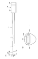
- FIG. 1 is an exploded perspective view for explaining the overall configuration of the electronic pen 100 of this embodiment.
- the electronic pen 100 of this embodiment is a tubular body that houses the electronic pen main body 1 and the electronic pen main body 1, and has a substantially cross section in a direction orthogonal to the axial direction.
- the electronic pen housing 2 having a triangular shape is provided.
- the rear end of the electronic pen main body 1 houses a connector portion described later, and is a tubular body connected to the rear end side of the electronic pen housing 2 and has a cross section in a direction orthogonal to the axial direction.
- a connector housing 4 that matches the cross section of the electronic pen housing 2 is provided. That is, the connector housing 4 has a substantially triangular cross section which is the same as the cross section of the electronic pen housing 2. Therefore, when the connector housing 4 is connected to the electronic pen housing 2, one electronic pen 100 can be configured without causing a step between the housings.
- the electronic pen main body 1 includes, for example, a pipe portion 11 made of a metal material. Inside the pipe portion 11, main parts for realizing the electronic pen function, such as a circuit board on which an electronic circuit described later is mounted and a core body constituting a center electrode, are housed. On the pen tip (tip) side of the pipe portion 11, a tubular shape formed of a conductive material such as metal via a link-shaped coupling member 12 formed of a resin material (insulating material) such as plastic. Peripheral electrodes 13 are connected.
- the peripheral electrode 13 is formed by integrally forming two portions, a tubular portion 13b having the same outer diameter as the pipe portion 11 and a tapered portion 13a.
- a ring-shaped front cap 14 formed of a resin material (insulating material) such as plastic is provided at the tip of the peripheral electrode 13. From the opening of the front cap 14, the tip portion of the core body (center electrode) 15 formed of a conductive material such as a conductive polyacetal resin protrudes to form a pen tip. Further, on the side surface of the pipe portion 11 of the electronic pen main body portion 1, a side switch portion 16 provided with two side switches is provided in this embodiment.
- the electronic pen housing 2 in which the electronic pen main body 1 is housed is, for example, a pipe-shaped one made of a resin material such as plastic, and the pen tip (tip) side is tapered (tapered). is there.
- the electronic pen housing 2 can also be formed of a non-conductive material other than resin, such as wood.
- Holes 21A and 21B for side switches are provided on the side surface of the electronic pen housing 2. These holes 21A and 21B are provided at positions corresponding to each of the two side switches in the side switch portion 16 of the electronic pen main body 1 housed in the electronic pen housing 2.
- Operation buttons 22A and 22B made of resin such as plastic are fitted into the holes 21A and 21B for these side switches.
- the operation buttons 22A and 22B are pushed into the electronic pen housing 2 by pressing, and return to the position before pressing when the pressing is released.
- the side switch provided on the electronic pen main body 1 can be pressed via the operation buttons 22A and 22B.
- the side switch in the electronic pen corresponds to a so-called left-click button or right-click button of a mouse, which is a pointing device of a personal computer. Therefore, by operating the side switch, in an electronic device such as a pen tablet equipped with a position detection device, for example, a window menu can be displayed and a target item can be selected.
- the connector housing 4 provided on the rear end side of the electronic pen main body 1 is composed of a body 41 made of a resin material such as plastic and an end cap 42 made of a metal material.
- the body portion 41 and the end cap 42 have the same cross-sectional shape, and as shown in FIG. 1, no step is generated even if they are connected.
- the inside of the connector housing 4 having such an appearance is hollow, and a connector portion described later is mounted on the connector housing 4.
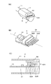
- FIG. 2 is a diagram for explaining the appearance of the electronic pen main body 1 and the connector housing 4 of the electronic pen of the embodiment.
- the electronic pen main body 1 and the connector housing 4 are connected to each other.
- the circuit board mounted on the pipe portion 11 of the electronic pen main body 1 and the connector board mounted on the connector housing 4 to be described later are electrically connected, and both boards are further fixed to each other.
- the connection method in this case various methods can be used.
- a jack (receptacle) type connection portion is provided at the rear end portion of the circuit board mounted on the pipe portion 11 of the electronic pen main body portion 1, and the tip portion of the connector board mounted on the connector housing 4 is provided.
- a plug (outlet) type connection is provided at the rear end portion of the circuit board mounted on the pipe portion 11 of the electronic pen main body portion 1, and the tip portion of the connector board mounted on the connector housing 4 is provided.
- a plug (outlet) type connection is provided at the rear end portion of the circuit board mounted on the pipe portion 11 of the electronic pen main
- FIG. 2B shows a state in which the base portion 32A and the contact portion 32B constituting the terminal portion of the connector portion mounted on the connector housing 4 can be seen from the opening 42H.
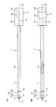
- FIG. 3 is a diagram for explaining the details of the connector portion of the electronic pen of the embodiment.
- FIG. 3A is a perspective view of the connector housing 4 portion as viewed from the rear end surface side. As shown by the rear end surface of the end cap 42, the cross-sectional shape of the connector housing 4 including the body portion 41 and the end cap 42 in the direction intersecting the axial direction is substantially triangular. An opening 42H for inserting and removing the plug is provided. A connector portion 3 is mounted in the back of the opening 42H. That is, the connector housing 4 is configured with a jack portion (receptacle) into which the connector plug (insertion port) is inserted.
- jack portion receptacle
- the connector portion 3 is composed of a connector board 31 and a terminal portion 32.
- the terminal portion 32 is located on the rear end side of the connector board 31 in the axial direction from a position separated from the base portion 32A that rises in the direction intersecting the axial direction J and the rear end surface of the base portion 32A. It is composed of a contact portion 32B extending toward the rear end side along J.
- the terminal portion 32 is composed of the base portion 32A and the contact portion 32B, and the contact portion 32B is located at a position eccentric from the axial center of the connector substrate 31.
- the end cap 42 portion of the connector housing 4 has a connector composed of the connector board 31 and the terminal portion 32.
- the part 3 is inserted and fixed.
- the contact portion 32B is positioned at the central portion of the opening 42H.
- the end cap 42 is made of a metal material and realizes the function of the shell portion of the connector portion 3. That is, the end cap 42 constitutes the outer shell of the connector portion 3, securely holds and protects the connector portion 3, and can regulate the position when the plug is fitted.
- the end cap 42 is made of a metal material, it also has a function of preventing noise from being mixed in from the outside. In this way, the connector housing 4 and the connector portion 3 form a connector for the electronic pen 100.
- FIG. 3C shows a state in which the front end portion of the connector board 31 of the connector portion 3 and the rear end portion of the circuit board 1C mounted on the pipe portion 11 of the electronic pen main body 1 are connected.
- the positional relationship between the electronic pen main body 1 and the connector 3 is important.
- FIG. 4 is a diagram for explaining the positional relationship between the electronic pen main body 1 and the connector 3 of the electronic pen 100 of the embodiment.
- FIG. 4A is a view of the side switch portion 16 provided on the electronic pen main body 1 when viewed from the side surface direction thereof
- FIG. 4B is a side switch provided on the electronic pen main body 1.
- 16 is a view when viewed from the upper surface direction thereof.
- FIG. 4 shows a case where the electronic pen main body 1 and the connector 3 provided in the connector housing 4 are connected. That is, FIG. 4 shows a state in which the circuit board mounted on the electronic pen main body 1 and the connector board 31 mounted on the connector housing 4 are connected.
- the axis J1 of the electronic pen main body 1 and the connector board 31 of the connector 3 mounted on the connector housing 4 are viewed from either side. It is made to coincide with the axis J2. Further, in this embodiment, although not shown, the axis of the circuit board 1C mounted on the pipe portion 11 of the electronic pen main body 1 is set to coincide with the axial center J1 of the electronic pen main body 1. .. As a result, when the electronic pen housing 2 on which the electronic pen main body 1 is mounted is connected (attached) to the connector housing 4 on which the connector portion 3 is mounted, the axis J2 of the connector board 31 becomes , Consistent with the axis J1 of the electronic pen main body 1.
- the axis of the electronic pen 100 passes through the axis of the electronic pen main body 1 from the tip (pen tip) of the core body 15 of the electronic pen 100 of this embodiment to the rear end surface of the end cap 42. It is configured to pass through the axis of the connector board 31.
- the applied pressure can be received through the axis of the electronic pen 100. Excessive pressure is not applied to only one of the parts. Therefore, it is possible to construct an electronic pen that is strong against the pressure applied from the pen tip direction to the rear end side and is also strong against the pressure applied from the rear end side to the pen tip side. In other words, it is possible to construct an electronic pen having high durability against both the pressure applied from the pen tip direction to the rear end side and the pressure applied from the rear end side to the pen tip side.
- the width of the connector board 31 is set to be equal to or less than the width of the terminal portion 32 (the portion including the base portion 32A and the contact portion 32B). As a result, it is possible to prevent the electronic pen 100 from being thinned. That is, if the width of the connector board 31 is configured to be the same as or shorter than the width of the terminal portion 32, it is not necessary to increase the cross-sectional area of the connector housing 4 under the influence of the connector board 31.
- the connector portion 3 of this embodiment corresponds to, for example, the USB standard type C.
- the present invention is not limited to this, and the connector portion 3 provided in the electronic pen 100 of this embodiment can be, for example, various types of connectors of the USB standard.
- the end cap 42 of the connector housing 4 can be used as the shell portion, so that it is not necessary to separately provide the shell portion that covers the contact portion, and the electronic pen is thin. Has been realized.
- the connector portion 3 of this embodiment is not limited to the one of the USB standard. It is compatible with connectors of various standards other than the USB standard. For example, it is possible to configure the connector portion so as to correspond to a connector having only a power supply terminal for charging. It is also possible to configure the connector portion so as to correspond to a connector having only terminals for transmitting and receiving data.
- FIG. 5 is a diagram for explaining the appearance of the electronic pen of the embodiment.
- the electronic pen 100 of this embodiment has an appearance similar to a so-called pencil.
- the connector connection function is realized by connecting the connector housing 4 to the rear end of the electronic pen housing 2. Further, from the tip of the electronic pen housing 2, the tapered portion 13a of the peripheral electrode 13 of the electronic pen main body 1 and the tip portion of the front cap 14 and the core body 15 project to realize the AES type electronic pen function.
- the total length (length in the longitudinal direction) of the electronic pen 100 of this embodiment is, for example, about 13 cm to 16 cm, which is about the same as or slightly shorter than a commercially available ballpoint pen or mechanical pencil.
- the cross section of the connector housing 4 is a substantially triangular shape in which the apex portion of an equilateral triangle is rounded, and the approximate length of one side is 10 mm. It is said to be a degree. Therefore, as described above, since the end cap 42 constitutes the shell portion, it is possible to mount the connector portion matching the USB standard type C having a width of the shell portion of 9 mm on the connector housing 4.
- the diameter of the pipe portion 11 of the electronic pen main body portion 1 is, for example, about 4 mm to 6 mm. Of course, the size shown here is an example and can be adjusted to various sizes.
- FIG. 6 is a diagram for explaining a configuration example of an electronic circuit portion that realizes the electronic pen function of the electronic pen 100.
- the control circuit 101, the signal transmission circuit 102, the signal reception circuit 103, the switch circuit 104, the changeover switch circuit 105, the charging circuit 106, and the battery 107 shown in FIG. 6 are circuits mounted on the pipe portion 11 of the electronic pen main body 1. It is a circuit part configured on the board 1C.
- the control circuit 101 is realized by an IC (Integrated Circuit) mounted on the circuit board 1C.
- the switches (described as SW in FIG. 6) 16A and 16B form a side switch provided in the side switch unit 16 and are pressed and operated through the operation buttons 22A and 22B, and the operation state is the control circuit. It is designed to notify 101.
- the signal transmission circuit 102 and the signal reception circuit 103 are connected to the control circuit 101, and the variable capacitance capacitor 5C constituting the pen pressure detection unit is also connected.
- the variable capacitance capacitor 5C is pressed by the core body 15, and the capacitance, that is, the capacitance charged on the positive electrode and the negative electrode can be changed according to the pressing force.
- a resistor 5R is connected in parallel to the variable capacitor 5C.
- the signal output end of the signal transmission circuit 102 is connected to the core body 15 through the switch circuit 104. Further, in this example, the signal output end of the signal transmission circuit 102 is connected to the terminal S of the changeover switch circuit 105.
- the movable terminal M of the changeover switch circuit 105 is connected to the peripheral electrode 13.
- the terminal R of the changeover switch circuit 105 is connected to the input end of the signal receiving circuit 103. Further, the terminal G of the changeover switch circuit 105 is connected to the ground electrode (ground electrode).
- the control circuit 101 supplies the switch circuit 104 with a control signal SW1 that controls the switch circuit 104 on / off. Further, the control circuit 101 supplies the changeover control signal SW2 to the changeover switch circuit 105 to switch whether the movable terminal M is connected to the terminal S, the terminal R, or the terminal G.
- the voltage of the battery 107 is supplied as a power supply voltage to each of the control circuit 101, the signal transmission circuit 102, the signal reception circuit 103, the switch circuit 104, and the changeover switch circuit 105.
- the battery 107 can be charged by the charging voltage formed in the charging circuit 106 from the external power supplied from the outside through the connector portion 3 described above.
- the signal receiving circuit 103 receives the signal received by the peripheral electrode 13 via the capacitance coupling (electrical coupling) with the position detecting sensor of the position detecting device, and demodulates or the like according to the received signal. The processing is performed, and the signal of the processing result is sent to the control circuit 101.
- the control circuit 101 analyzes the signal from the signal receiving circuit 103, determines the specifications of the other party's position detection device, and determines the timing of signal interaction with the position detection sensor of the other party's position detection device.
- the control circuit 101 controls the format of the signal output from the signal transmission circuit 102 so as to match the specifications of the position detection device of the other party, and interacts with the position detection sensor at a predetermined timing.
- the signal transmission circuit 102 basically includes a position detection signal (burst signal) having a predetermined frequency for position detection by the position detection device, and pressure information according to the writing pressure detected by the variable capacitance capacitor 5C. Is output under the control of the control circuit 101.
- the signal transmission circuit 102 also outputs a signal for detecting the tilt angle of the electronic pen 100. That is, the signal transmission circuit 102 sends a burst signal for position detection and for detecting the tilt angle of the electronic pen 100 under the control of the control circuit 101.
- the control circuit 101 executes an operation of detecting the pen pressure based on the capacitance of the variable capacitance capacitor 5C constituting the pen pressure detection unit during the period of transmitting the burst signal for position detection from the signal transmission circuit 102. To do.
- the control circuit 101 first charges the variable-capacity capacitor 5C to a fully charged state, and then stops charging to bring the variable-capacity capacitor 5C into a state of being discharged through the resistor 5R. The time from the start of discharge until the voltage across the variable capacitance capacitor 5C reaches a predetermined predetermined voltage is measured, and the capacitance of the variable capacitance capacitor 5C at that time is detected from that time. Since the capacitance of the variable capacitance capacitor 5C corresponds to the writing pressure applied to the core body 15 at that time, the writing pressure is detected based on the detected capacitance.
- the control circuit 101 converts the detected pen pressure into a multi-bit digital signal in this example, and outputs the pen pressure information corresponding to the digital signal from the signal transmission circuit 102. Control.
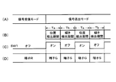
- FIG. 7 is a diagram used to explain the operation of a configuration example of the electronic circuit portion of the electronic pen 100.
- the control circuit 101 sets the electronic pen main body 1 in a signal reception mode for receiving a signal from the position detection sensor of the position detection device in a steady state.
- this signal reception mode after confirming the reception of the signal from the position detection device and performing the predetermined processing described above, the mode is switched to the signal transmission mode in which the signal is transmitted to the position detection device.
- the switch circuit 104 in the signal reception mode, the switch circuit 104 is turned off by the control signal SW1 (see FIG. 7C) from the control circuit 101, and the changeover switch circuit 105 is a movable terminal by the changeover control signal SW2. M is controlled to be connected to the terminal R (see FIG. 7 (D)).
- the signal from the position detection device received by the peripheral electrode 13 is supplied to the signal reception circuit 103 through the changeover switch circuit 105 and demodulated, and the demodulated received signal is the control circuit 101. Is supplied to.
- the control circuit 101 analyzes the received signal from the position detection device to determine the specifications of the other position detection device.
- the received signal from the position detection device includes information instructing the timing when the electronic pen main body 1 starts transmitting the signal. Therefore, based on the information instructing the timing, the control circuit 101 determines the switching timing from the signal reception mode to the signal transmission mode, and also determines the timing of the time division processing in the signal transmission mode. To do. After that, the control circuit 101 switches the electronic pen main body 1 from the signal reception mode to the signal transmission mode.
- the tilt detection period Tb for detecting the tilt angle of 100 is executed in a time division manner.
- the switch circuit 104 is turned on by the control signal SW1 (see FIG. 7C), and the movable terminal M of the changeover switch circuit 105 is connected to the terminal G by the changeover control signal SW2. (See FIG. 7 (D)). Therefore, during the position detection period Ta, the peripheral electrode 13 is connected to the ground electrode through the changeover switch circuit 105. Then, the control circuit 101 controls the signal transmission circuit 102 so as to output the burst signal of the position detection signal and the pen pressure information during the position detection period Ta. The position detection signal and pen pressure information output from the signal transmission circuit 102 are supplied to the core 15 through the switch circuit 104 and sent to the position detection sensor. In this case, the control circuit 101 controls the signal transmission circuit 102 so that the pen pressure information is transmitted from the core body 15 after the burst signal transmission period ends.
- the peripheral electrode 13 is connected to the ground electrode, the core body 15 is shielded except for the tip portion 15a which is the pen tip thereof. Therefore, the signal from the signal transmission circuit 102 is transmitted from the tip portion 15a of the core body 15 without being affected by the outside.
- the switch circuit 104 is turned off by the control signal SW1 (see FIG. 7C), and the changeover switch circuit 105 has the movable terminal M as the terminal S by the changeover control signal SW2. (See FIG. 7 (D)).
- the control circuit 101 controls the signal transmission circuit 102 so as to generate a burst signal for inclination detection.
- the burst signal for tilt detection is a signal having the same frequency as the burst signal of the position detection signal.
- the burst signal for tilt detection from the signal transmission circuit 102 is supplied to the peripheral electrode 13 through the changeover switch circuit 105 and sent to the position detection sensor.
- the position detection device that receives the burst signal for tilt detection through the position detection sensor detects the tilt angle of the electronic pen 100 as described later.
- FIG. 8 is a diagram for explaining the detection of the tilt angle of the electronic pen 100 performed on the position detecting device side based on the signal from the electronic pen 100 of the embodiment.
- the electrostatically coupled region OBa is a perfect circular region as shown in FIG. 8 (B).
- the peripheral electrode 13 and the position detection sensor 200 are electrostatically coupled, and the electrostatically coupled region OBb is a ring-shaped region as shown in FIG. 8C. ..
- the core body 15 of the electronic pen main body 1 of the electronic pen 100 is tilted with respect to the input surface of the position detection sensor 200.
- the region OBa that electrostatically couples between the tip portion 15a of the core body 15 and the position detection sensor 200 during the position detection period Ta remains a substantially perfect circular region as shown in FIG. 8 (E).
- the region OBb that electrostatically couples between the peripheral electrode 13 and the position detection sensor 200 is an ellipse that corresponds to the tilt angle and extends long in the tilt direction, as shown in FIG. 8 (F). It becomes the area of the shape.
- the control circuit of the position detection device can detect the magnitude of the tilt angle of the electronic pen 100 from the elliptical length of the region OBb shown in FIG. 8 (F) in the oval direction. Further, the direction of inclination of the electronic pen 100 can be detected by detecting the elliptical elliptical direction of the region OBb starting from the designated position of the electronic pen 100 shown in FIG. 8 (E).
- the peripheral electrode 13 used to detect the tilt angle may use a signal having the same frequency as the signal supplied to the core body 15, but the frequency of the signal supplied to the core body 15 may be used. , The frequency of the signal supplied to the peripheral electrode 13 may be different. In that case, the position detection device can distinguish between the signal from the core body 15 and the signal from the peripheral electrode 13.
- the position detection period Ta and the inclination detection period Tb are not executed in a time division manner as described above, but the signal from the core body 15 and the peripheral electrode 13 are used.
- the signal may be configured to be simultaneously transmitted to the position detection sensor 200.
- the position detection device can process the electronic pen 100 to simultaneously detect the indicated position and the inclination of the electronic pen 100.
- control circuit 101 and the connector portion 3 are electrically connected. This indicates that information such as data and programs can be transmitted and received to and from an external device through the connector unit 3.
- control circuit 101 is configured as a so-called microprocessor composed of, for example, a CPU (Central Processing unit), a ROM (Read only Memory), a RAM (Random Access Memory) non-volatile memory, and the like.
- various setting information and the like are provided by an external device, a program for operating the electronic pen is provided, and pen pressure information stored in the electronic pen 100 is supplied to the external device. You will be able to provide things such as.
- the electronic pen 100 of the above-described embodiment can be made thinner by providing the connector portion in the connector housing 4 having a substantially triangular cross section.
- the connector housing 4 having a substantially triangular cross section.
- the axis of the electronic pen 100 passes through the axis of the electronic pen body 1 and the axis of the connector substrate 31. It can be configured to pass through the heart. This makes it possible to construct an electronic pen that is strong against the pressure applied from the pen tip direction to the rear end side and is also strong against the pressure applied from the rear end side to the pen tip side.
- connection configuration between the core 15 and the circuit board of the electronic pen body 1 and the connection configuration between the connector board 31 and the electronic pen is not complicated. That is, even if the connector portion is provided, the configuration can be prevented from becoming particularly complicated as compared with the conventional electronic pen.
- the peripheral electrode 13 is used for detecting the tilt angle of the electronic pen 100, but the present invention is not limited to this.
- the peripheral electrode 13 can function as a shield electrode that prevents noise from being mixed into the core body 15.
- the electronic pen housing 2 has been described as having a substantially triangular cross section like the connector housing 4, but the present invention is not limited to this.
- the electronic pen housing 2 may have any cross-sectional shape as long as it can accommodate the electronic pen main body 1. However, if the cross-sectional shape of the electronic pen housing 2 and the cross-sectional shape of the connector housing 4 are matched as in the above-described embodiment, the electronic pen has no step on the side surface even when both are connected. Can be configured.
- the present invention is not limited to this.
- an EMR type electronic pen it may be necessary to send / receive data or a program in order to improve the functionality.
- a short-range wireless communication function of the Bluetooth (registered trademark) standard may be installed. In such a case, the power supply voltage is supplied. It may be necessary to install a battery for this purpose and charge it.
- the present invention can be applied to an EMR type electronic pen, and a connector portion can be provided at the rear end portion of the electronic pen.
- Control circuit 102 ... Signal transmission circuit, 103 ... Signal reception circuit, 104 ... Switch circuit, 105 ... Changeover switch circuit, 106 ... Charging circuit, 107 ... Battery, 5C ... Variable capacitance capacitor, 5R ... Resistance
Abstract
L'invention concerne un stylo électronique qui peut avoir une structure non compliquée même si une partie de raccordement est prévue, et qui a une résistance suffisante pour supporter une pression d'écriture et une charge appliquée pendant l'insertion/le retrait d'un bouchon et qui est également mince. Au moins un boîtier de raccordement (4) a une section transversale sensiblement triangulaire dans une direction orthogonale à la direction axiale. À l'intérieur d'un boîtier de stylo électronique se trouve une partie de corps de stylo électronique (1), et à l'intérieur du boîtier de raccordement (4) se trouve une partie de raccordement (3). La partie de raccordement (3) comprend : un substrat de raccordement (31); et une section de borne (32) comprenant une partie de base et une partie de contact. Dans un état dans lequel le boîtier de raccordement (4) est fixé au boîtier de stylo électronique, l'axe du substrat de raccordement (31) coïncide avec l'axe de la partie de corps de stylo électronique (1).
Priority Applications (4)
| Application Number | Priority Date | Filing Date | Title |
|---|---|---|---|
| CN202080071463.0A CN114514495A (zh) | 2019-11-08 | 2020-10-27 | 电子笔 |
| JP2021554901A JPWO2021090728A1 (fr) | 2019-11-08 | 2020-10-27 | |
| US17/725,225 US11893173B2 (en) | 2019-11-08 | 2022-04-20 | Electronic pen |
| US18/405,835 US20240152219A1 (en) | 2019-11-08 | 2024-01-05 | Electronic pen |
Applications Claiming Priority (2)
| Application Number | Priority Date | Filing Date | Title |
|---|---|---|---|
| JP2019203411 | 2019-11-08 | ||
| JP2019-203411 | 2019-11-08 |
Related Child Applications (1)
| Application Number | Title | Priority Date | Filing Date |
|---|---|---|---|
| US17/725,225 Continuation US11893173B2 (en) | 2019-11-08 | 2022-04-20 | Electronic pen |
Publications (1)
| Publication Number | Publication Date |
|---|---|
| WO2021090728A1 true WO2021090728A1 (fr) | 2021-05-14 |
Family
ID=75848360
Family Applications (1)
| Application Number | Title | Priority Date | Filing Date |
|---|---|---|---|
| PCT/JP2020/040160 WO2021090728A1 (fr) | 2019-11-08 | 2020-10-27 | Stylo électronique |
Country Status (4)
| Country | Link |
|---|---|
| US (2) | US11893173B2 (fr) |
| JP (1) | JPWO2021090728A1 (fr) |
| CN (1) | CN114514495A (fr) |
| WO (1) | WO2021090728A1 (fr) |
Citations (3)
| Publication number | Priority date | Publication date | Assignee | Title |
|---|---|---|---|---|
| JP2018531444A (ja) * | 2015-09-08 | 2018-10-25 | アップル インコーポレイテッドApple Inc. | 電子デバイス用スタイラス |
| WO2018207540A1 (fr) * | 2017-05-10 | 2018-11-15 | 第一精工株式会社 | Connecteur |
| JP2019114212A (ja) * | 2017-12-26 | 2019-07-11 | 株式会社ワコム | 電子ペン |
Family Cites Families (6)
| Publication number | Priority date | Publication date | Assignee | Title |
|---|---|---|---|---|
| US7567241B2 (en) * | 2004-08-03 | 2009-07-28 | Silverbrook Research Pty Ltd | Stylus with customizable appearance |
| US7825913B2 (en) * | 2007-01-30 | 2010-11-02 | Hewlett-Packard Development Company, L.P. | Computer stylus with integrated memory |
| TWI480770B (zh) * | 2014-06-27 | 2015-04-11 | Waltop Int Corp | 電容式指標裝置 |
| GB2531324B (en) * | 2014-10-16 | 2018-01-10 | Scriba Stylus (Ip) Ltd | A stylus |
| TWI771371B (zh) * | 2017-04-27 | 2022-07-21 | 日商和冠股份有限公司 | 充電式電子筆 |
| CN108334213A (zh) * | 2018-03-07 | 2018-07-27 | 精模电子科技(深圳)有限公司 | 电容触控笔 |
-
2020
- 2020-10-27 JP JP2021554901A patent/JPWO2021090728A1/ja active Pending
- 2020-10-27 WO PCT/JP2020/040160 patent/WO2021090728A1/fr active Application Filing
- 2020-10-27 CN CN202080071463.0A patent/CN114514495A/zh active Pending
-
2022
- 2022-04-20 US US17/725,225 patent/US11893173B2/en active Active
-
2024
- 2024-01-05 US US18/405,835 patent/US20240152219A1/en active Pending
Patent Citations (3)
| Publication number | Priority date | Publication date | Assignee | Title |
|---|---|---|---|---|
| JP2018531444A (ja) * | 2015-09-08 | 2018-10-25 | アップル インコーポレイテッドApple Inc. | 電子デバイス用スタイラス |
| WO2018207540A1 (fr) * | 2017-05-10 | 2018-11-15 | 第一精工株式会社 | Connecteur |
| JP2019114212A (ja) * | 2017-12-26 | 2019-07-11 | 株式会社ワコム | 電子ペン |
Also Published As
| Publication number | Publication date |
|---|---|
| US11893173B2 (en) | 2024-02-06 |
| US20220244798A1 (en) | 2022-08-04 |
| JPWO2021090728A1 (fr) | 2021-05-14 |
| CN114514495A (zh) | 2022-05-17 |
| US20240152219A1 (en) | 2024-05-09 |
Similar Documents
| Publication | Publication Date | Title |
|---|---|---|
| US10739873B2 (en) | Transmission-type electronic pen | |
| JP6756525B2 (ja) | 筆記具及び電子ペン本体部 | |
| US10459539B2 (en) | Electronic pen and electronic pen main body | |
| TWI751993B (zh) | 電子筆 | |
| TWI685774B (zh) | 位置指示器 | |
| EP3279773B1 (fr) | Stylo électronique | |
| CN110520828B (zh) | 位置指示器 | |
| US11868571B2 (en) | Capacitive electronic pen including detachable axial core body | |
| US20240103649A1 (en) | Electronic pen and cartridge-type electronic pen main body including an conductive center electrode and a peripheral electrode | |
| EP4012538A1 (fr) | Stylo électronique et corps de stylo électronique | |
| WO2021090728A1 (fr) | Stylo électronique | |
| JP6150369B1 (ja) | 電子ペン | |
| US11614808B2 (en) | Electronic pen | |
| GB2569945A (en) | Tip and stylus having the same |
Legal Events
| Date | Code | Title | Description |
|---|---|---|---|
| 121 | Ep: the epo has been informed by wipo that ep was designated in this application |
Ref document number: 20885819 Country of ref document: EP Kind code of ref document: A1 |
|
| ENP | Entry into the national phase |
Ref document number: 2021554901 Country of ref document: JP Kind code of ref document: A |
|
| NENP | Non-entry into the national phase |
Ref country code: DE |
|
| 122 | Ep: pct application non-entry in european phase |
Ref document number: 20885819 Country of ref document: EP Kind code of ref document: A1 |