WO2021090728A1 - Electronic pen - Google Patents
Electronic pen Download PDFInfo
- Publication number
- WO2021090728A1 WO2021090728A1 PCT/JP2020/040160 JP2020040160W WO2021090728A1 WO 2021090728 A1 WO2021090728 A1 WO 2021090728A1 JP 2020040160 W JP2020040160 W JP 2020040160W WO 2021090728 A1 WO2021090728 A1 WO 2021090728A1
- Authority
- WO
- WIPO (PCT)
- Prior art keywords
- electronic pen
- connector
- housing
- main body
- signal
- Prior art date
Links
Images


Classifications
-
- G—PHYSICS
- G06—COMPUTING; CALCULATING OR COUNTING
- G06F—ELECTRIC DIGITAL DATA PROCESSING
- G06F3/00—Input arrangements for transferring data to be processed into a form capable of being handled by the computer; Output arrangements for transferring data from processing unit to output unit, e.g. interface arrangements
- G06F3/01—Input arrangements or combined input and output arrangements for interaction between user and computer
- G06F3/03—Arrangements for converting the position or the displacement of a member into a coded form
- G06F3/033—Pointing devices displaced or positioned by the user, e.g. mice, trackballs, pens or joysticks; Accessories therefor
- G06F3/0354—Pointing devices displaced or positioned by the user, e.g. mice, trackballs, pens or joysticks; Accessories therefor with detection of 2D relative movements between the device, or an operating part thereof, and a plane or surface, e.g. 2D mice, trackballs, pens or pucks
- G06F3/03545—Pens or stylus
-
- G—PHYSICS
- G06—COMPUTING; CALCULATING OR COUNTING
- G06F—ELECTRIC DIGITAL DATA PROCESSING
- G06F3/00—Input arrangements for transferring data to be processed into a form capable of being handled by the computer; Output arrangements for transferring data from processing unit to output unit, e.g. interface arrangements
- G06F3/01—Input arrangements or combined input and output arrangements for interaction between user and computer
- G06F3/03—Arrangements for converting the position or the displacement of a member into a coded form
- G06F3/033—Pointing devices displaced or positioned by the user, e.g. mice, trackballs, pens or joysticks; Accessories therefor
- G06F3/0346—Pointing devices displaced or positioned by the user, e.g. mice, trackballs, pens or joysticks; Accessories therefor with detection of the device orientation or free movement in a 3D space, e.g. 3D mice, 6-DOF [six degrees of freedom] pointers using gyroscopes, accelerometers or tilt-sensors
-
- G—PHYSICS
- G06—COMPUTING; CALCULATING OR COUNTING
- G06F—ELECTRIC DIGITAL DATA PROCESSING
- G06F3/00—Input arrangements for transferring data to be processed into a form capable of being handled by the computer; Output arrangements for transferring data from processing unit to output unit, e.g. interface arrangements
- G06F3/01—Input arrangements or combined input and output arrangements for interaction between user and computer
- G06F3/03—Arrangements for converting the position or the displacement of a member into a coded form
- G06F3/033—Pointing devices displaced or positioned by the user, e.g. mice, trackballs, pens or joysticks; Accessories therefor
- G06F3/038—Control and interface arrangements therefor, e.g. drivers or device-embedded control circuitry
- G06F3/0383—Signal control means within the pointing device
-
- H—ELECTRICITY
- H01—ELECTRIC ELEMENTS
- H01R—ELECTRICALLY-CONDUCTIVE CONNECTIONS; STRUCTURAL ASSOCIATIONS OF A PLURALITY OF MUTUALLY-INSULATED ELECTRICAL CONNECTING ELEMENTS; COUPLING DEVICES; CURRENT COLLECTORS
- H01R13/00—Details of coupling devices of the kinds covered by groups H01R12/70 or H01R24/00 - H01R33/00
- H01R13/46—Bases; Cases
- H01R13/52—Dustproof, splashproof, drip-proof, waterproof, or flameproof cases
- H01R13/5213—Covers
-
- H—ELECTRICITY
- H01—ELECTRIC ELEMENTS
- H01R—ELECTRICALLY-CONDUCTIVE CONNECTIONS; STRUCTURAL ASSOCIATIONS OF A PLURALITY OF MUTUALLY-INSULATED ELECTRICAL CONNECTING ELEMENTS; COUPLING DEVICES; CURRENT COLLECTORS
- H01R13/00—Details of coupling devices of the kinds covered by groups H01R12/70 or H01R24/00 - H01R33/00
- H01R13/648—Protective earth or shield arrangements on coupling devices, e.g. anti-static shielding
- H01R13/658—High frequency shielding arrangements, e.g. against EMI [Electro-Magnetic Interference] or EMP [Electro-Magnetic Pulse]
- H01R13/6581—Shield structure
-
- H—ELECTRICITY
- H01—ELECTRIC ELEMENTS
- H01R—ELECTRICALLY-CONDUCTIVE CONNECTIONS; STRUCTURAL ASSOCIATIONS OF A PLURALITY OF MUTUALLY-INSULATED ELECTRICAL CONNECTING ELEMENTS; COUPLING DEVICES; CURRENT COLLECTORS
- H01R13/00—Details of coupling devices of the kinds covered by groups H01R12/70 or H01R24/00 - H01R33/00
- H01R13/648—Protective earth or shield arrangements on coupling devices, e.g. anti-static shielding
- H01R13/658—High frequency shielding arrangements, e.g. against EMI [Electro-Magnetic Interference] or EMP [Electro-Magnetic Pulse]
- H01R13/6591—Specific features or arrangements of connection of shield to conductive members
- H01R13/6594—Specific features or arrangements of connection of shield to conductive members the shield being mounted on a PCB and connected to conductive members
-
- H—ELECTRICITY
- H05—ELECTRIC TECHNIQUES NOT OTHERWISE PROVIDED FOR
- H05K—PRINTED CIRCUITS; CASINGS OR CONSTRUCTIONAL DETAILS OF ELECTRIC APPARATUS; MANUFACTURE OF ASSEMBLAGES OF ELECTRICAL COMPONENTS
- H05K5/00—Casings, cabinets or drawers for electric apparatus
- H05K5/0026—Casings, cabinets or drawers for electric apparatus provided with connectors and printed circuit boards [PCB], e.g. automotive electronic control units
- H05K5/0039—Casings, cabinets or drawers for electric apparatus provided with connectors and printed circuit boards [PCB], e.g. automotive electronic control units having a tubular housing wherein the PCB is inserted longitudinally
-
- G—PHYSICS
- G06—COMPUTING; CALCULATING OR COUNTING
- G06F—ELECTRIC DIGITAL DATA PROCESSING
- G06F3/00—Input arrangements for transferring data to be processed into a form capable of being handled by the computer; Output arrangements for transferring data from processing unit to output unit, e.g. interface arrangements
- G06F3/01—Input arrangements or combined input and output arrangements for interaction between user and computer
- G06F3/03—Arrangements for converting the position or the displacement of a member into a coded form
- G06F3/041—Digitisers, e.g. for touch screens or touch pads, characterised by the transducing means
- G06F3/044—Digitisers, e.g. for touch screens or touch pads, characterised by the transducing means by capacitive means
- G06F3/0446—Digitisers, e.g. for touch screens or touch pads, characterised by the transducing means by capacitive means using a grid-like structure of electrodes in at least two directions, e.g. using row and column electrodes
-
- G—PHYSICS
- G06—COMPUTING; CALCULATING OR COUNTING
- G06F—ELECTRIC DIGITAL DATA PROCESSING
- G06F3/00—Input arrangements for transferring data to be processed into a form capable of being handled by the computer; Output arrangements for transferring data from processing unit to output unit, e.g. interface arrangements
- G06F3/01—Input arrangements or combined input and output arrangements for interaction between user and computer
- G06F3/03—Arrangements for converting the position or the displacement of a member into a coded form
- G06F3/041—Digitisers, e.g. for touch screens or touch pads, characterised by the transducing means
- G06F3/046—Digitisers, e.g. for touch screens or touch pads, characterised by the transducing means by electromagnetic means
Definitions
- the present invention relates to an electronic pen for inputting information through a position detecting device.
- a battery-powered electronic pen is used to transmit a signal to the sensor unit of the position detection device.
- the electronic pen is equipped with a rechargeable battery, it is necessary to provide a connector for charging the rechargeable battery. Further, in recent years, in order to improve the functionality of the electronic pen, it may be necessary to send and receive data and programs between the electronic pen and an external device such as a personal computer, and a connector for transmitting and receiving data. There is also a need to provide.
- Patent Document 1 described later describes a connector on the rear end side of the tubular housing of the electronic pen so that a USB (Universal Serial Bus) standard plug can be inserted and removed from the rear end surface.
- the invention relating to the electronic pen in which the above is arranged is disclosed.
- the invention described in Patent Document 1 is to provide a USB standard connector centered on the diameter of the circular rear end surface of the electronic pen, and the connector portion does not interfere with the use of the electronic pen. , The plug can be inserted and removed properly.
- the connector portion is made of metal and has a housing including a contact portion provided with a plurality of terminals and a base portion for holding the contact portion in a hollow shape. It is composed by covering with a shell part.
- the shell portion constitutes the outer shell of the connector portion, and is a member for securely holding and protecting the housing and determining the position when the plug is fitted.
- the core portion is also provided at a position deviated from the axis of the circuit board. Therefore, not only the connector portion but also the configuration of the connection portion between the pen tip side and the circuit board may be complicated. Further, in this case, the axis of the electronic pen and the axis of the circuit board do not match, and the load applied to the circuit board is large due to the writing pressure on the core and the pressure when the plug is attached to the connector. I'm worried about becoming.
- the present invention does not complicate the configuration even if the connector portion is provided, has sufficient strength to withstand the pen pressure and the load applied when inserting and removing the plug, and further reduces the size.
- the purpose is to provide an electronic pen that can be realized.
- An electronic pen housing that is a tubular body that houses the electronic pen body, It consists of a connector board, a base portion that rises from the connector board in a direction intersecting the axial direction, and a contact portion that extends from a position separated from the connector board on the rear end surface of the base portion to the rear end side.
- the electronic pen housing and the connector housing are connected to each other and both are tubular bodies, but at least the connector housing has a cross section in a direction orthogonal to the axial direction. However, it has a substantially triangular shape.
- the electronic pen main body is housed in the electronic pen housing, and the connector housing is extended from a position separated from the connector board, the base portion rising from the connector board, and the connector board on the rear end surface of the base portion.
- a connector portion composed of a terminal portion composed of a contact portion is housed. Therefore, the contact portion of the terminal portion is formed at a position eccentric from the axial center of the connector substrate.
- the position detection device includes a sensor unit in which a plurality of loop coils are arranged in each of the X-axis direction and the Y-axis direction. Then, a transmission period in which electric power is sequentially supplied to the plurality of loop coils of the sensor unit to generate a magnetic field and a reception period in which the supply of electric power is stopped and a magnetic field from the outside is received are alternately provided.
- the corresponding electronic pen is provided with a resonance circuit consisting of a coil and a capacitor, and a signal is generated by a current flowing through the coil in response to a magnetic field from the sensor unit, and the position including the pen pressure information in this signal. Send to the detection sensor. This is received by the position detection device during the reception period, and the position indicated by the electronic pen and the writing pressure are detected.
- the position detection device includes a sensor unit in which a plurality of linear conductors (line electrodes) are arranged in each of the X-axis direction and the Y-axis direction. Then, the sensor unit detects the indicated position according to the change in the capacitance (charge) generated in the linear conductor when the finger or the electrostatic pen is brought close to the sensor unit.
- the electrostatic pen includes a pen-type position indicator having conductivity or a so-called active electrostatic pen driven by a battery and transmitting a signal. In the case of the active electrostatic coupling method using an active electrostatic pen, the electronic pen transmits the signal from the oscillation circuit mounted on the electronic pen including the pen pressure information, and receives this by the position detection device. The indicated position and pen pressure are detected.
- the electronic pen of the invention of this application can be applied to various types of electronic pens. Therefore, the electronic pen of the invention of the present application is applicable to the above-mentioned electromagnetic induction type electronic pen and also to the active electrostatic coupling type electronic pen (active electrostatic pen).
- active electrostatic pen active electrostatic pen
- AES Active Electrostatic
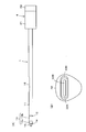
- FIG. 1 is an exploded perspective view for explaining the overall configuration of the electronic pen 100 of this embodiment.
- the electronic pen 100 of this embodiment is a tubular body that houses the electronic pen main body 1 and the electronic pen main body 1, and has a substantially cross section in a direction orthogonal to the axial direction.
- the electronic pen housing 2 having a triangular shape is provided.
- the rear end of the electronic pen main body 1 houses a connector portion described later, and is a tubular body connected to the rear end side of the electronic pen housing 2 and has a cross section in a direction orthogonal to the axial direction.
- a connector housing 4 that matches the cross section of the electronic pen housing 2 is provided. That is, the connector housing 4 has a substantially triangular cross section which is the same as the cross section of the electronic pen housing 2. Therefore, when the connector housing 4 is connected to the electronic pen housing 2, one electronic pen 100 can be configured without causing a step between the housings.
- the electronic pen main body 1 includes, for example, a pipe portion 11 made of a metal material. Inside the pipe portion 11, main parts for realizing the electronic pen function, such as a circuit board on which an electronic circuit described later is mounted and a core body constituting a center electrode, are housed. On the pen tip (tip) side of the pipe portion 11, a tubular shape formed of a conductive material such as metal via a link-shaped coupling member 12 formed of a resin material (insulating material) such as plastic. Peripheral electrodes 13 are connected.
- the peripheral electrode 13 is formed by integrally forming two portions, a tubular portion 13b having the same outer diameter as the pipe portion 11 and a tapered portion 13a.
- a ring-shaped front cap 14 formed of a resin material (insulating material) such as plastic is provided at the tip of the peripheral electrode 13. From the opening of the front cap 14, the tip portion of the core body (center electrode) 15 formed of a conductive material such as a conductive polyacetal resin protrudes to form a pen tip. Further, on the side surface of the pipe portion 11 of the electronic pen main body portion 1, a side switch portion 16 provided with two side switches is provided in this embodiment.
- the electronic pen housing 2 in which the electronic pen main body 1 is housed is, for example, a pipe-shaped one made of a resin material such as plastic, and the pen tip (tip) side is tapered (tapered). is there.
- the electronic pen housing 2 can also be formed of a non-conductive material other than resin, such as wood.
- Holes 21A and 21B for side switches are provided on the side surface of the electronic pen housing 2. These holes 21A and 21B are provided at positions corresponding to each of the two side switches in the side switch portion 16 of the electronic pen main body 1 housed in the electronic pen housing 2.
- Operation buttons 22A and 22B made of resin such as plastic are fitted into the holes 21A and 21B for these side switches.
- the operation buttons 22A and 22B are pushed into the electronic pen housing 2 by pressing, and return to the position before pressing when the pressing is released.
- the side switch provided on the electronic pen main body 1 can be pressed via the operation buttons 22A and 22B.
- the side switch in the electronic pen corresponds to a so-called left-click button or right-click button of a mouse, which is a pointing device of a personal computer. Therefore, by operating the side switch, in an electronic device such as a pen tablet equipped with a position detection device, for example, a window menu can be displayed and a target item can be selected.
- the connector housing 4 provided on the rear end side of the electronic pen main body 1 is composed of a body 41 made of a resin material such as plastic and an end cap 42 made of a metal material.
- the body portion 41 and the end cap 42 have the same cross-sectional shape, and as shown in FIG. 1, no step is generated even if they are connected.
- the inside of the connector housing 4 having such an appearance is hollow, and a connector portion described later is mounted on the connector housing 4.
- FIG. 2 is a diagram for explaining the appearance of the electronic pen main body 1 and the connector housing 4 of the electronic pen of the embodiment.
- the electronic pen main body 1 and the connector housing 4 are connected to each other.
- the circuit board mounted on the pipe portion 11 of the electronic pen main body 1 and the connector board mounted on the connector housing 4 to be described later are electrically connected, and both boards are further fixed to each other.
- the connection method in this case various methods can be used.
- a jack (receptacle) type connection portion is provided at the rear end portion of the circuit board mounted on the pipe portion 11 of the electronic pen main body portion 1, and the tip portion of the connector board mounted on the connector housing 4 is provided.
- a plug (outlet) type connection is provided at the rear end portion of the circuit board mounted on the pipe portion 11 of the electronic pen main body portion 1, and the tip portion of the connector board mounted on the connector housing 4 is provided.
- a plug (outlet) type connection is provided at the rear end portion of the circuit board mounted on the pipe portion 11 of the electronic pen main
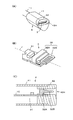
- FIG. 2B shows a state in which the base portion 32A and the contact portion 32B constituting the terminal portion of the connector portion mounted on the connector housing 4 can be seen from the opening 42H.
- FIG. 3 is a diagram for explaining the details of the connector portion of the electronic pen of the embodiment.
- FIG. 3A is a perspective view of the connector housing 4 portion as viewed from the rear end surface side. As shown by the rear end surface of the end cap 42, the cross-sectional shape of the connector housing 4 including the body portion 41 and the end cap 42 in the direction intersecting the axial direction is substantially triangular. An opening 42H for inserting and removing the plug is provided. A connector portion 3 is mounted in the back of the opening 42H. That is, the connector housing 4 is configured with a jack portion (receptacle) into which the connector plug (insertion port) is inserted.
- jack portion receptacle
- the connector portion 3 is composed of a connector board 31 and a terminal portion 32.
- the terminal portion 32 is located on the rear end side of the connector board 31 in the axial direction from a position separated from the base portion 32A that rises in the direction intersecting the axial direction J and the rear end surface of the base portion 32A. It is composed of a contact portion 32B extending toward the rear end side along J.
- the terminal portion 32 is composed of the base portion 32A and the contact portion 32B, and the contact portion 32B is located at a position eccentric from the axial center of the connector substrate 31.
- the end cap 42 portion of the connector housing 4 has a connector composed of the connector board 31 and the terminal portion 32.
- the part 3 is inserted and fixed.
- the contact portion 32B is positioned at the central portion of the opening 42H.
- the end cap 42 is made of a metal material and realizes the function of the shell portion of the connector portion 3. That is, the end cap 42 constitutes the outer shell of the connector portion 3, securely holds and protects the connector portion 3, and can regulate the position when the plug is fitted.
- the end cap 42 is made of a metal material, it also has a function of preventing noise from being mixed in from the outside. In this way, the connector housing 4 and the connector portion 3 form a connector for the electronic pen 100.
- FIG. 3C shows a state in which the front end portion of the connector board 31 of the connector portion 3 and the rear end portion of the circuit board 1C mounted on the pipe portion 11 of the electronic pen main body 1 are connected.
- the positional relationship between the electronic pen main body 1 and the connector 3 is important.
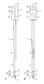
- FIG. 4 is a diagram for explaining the positional relationship between the electronic pen main body 1 and the connector 3 of the electronic pen 100 of the embodiment.
- FIG. 4A is a view of the side switch portion 16 provided on the electronic pen main body 1 when viewed from the side surface direction thereof
- FIG. 4B is a side switch provided on the electronic pen main body 1.
- 16 is a view when viewed from the upper surface direction thereof.
- FIG. 4 shows a case where the electronic pen main body 1 and the connector 3 provided in the connector housing 4 are connected. That is, FIG. 4 shows a state in which the circuit board mounted on the electronic pen main body 1 and the connector board 31 mounted on the connector housing 4 are connected.
- the axis J1 of the electronic pen main body 1 and the connector board 31 of the connector 3 mounted on the connector housing 4 are viewed from either side. It is made to coincide with the axis J2. Further, in this embodiment, although not shown, the axis of the circuit board 1C mounted on the pipe portion 11 of the electronic pen main body 1 is set to coincide with the axial center J1 of the electronic pen main body 1. .. As a result, when the electronic pen housing 2 on which the electronic pen main body 1 is mounted is connected (attached) to the connector housing 4 on which the connector portion 3 is mounted, the axis J2 of the connector board 31 becomes , Consistent with the axis J1 of the electronic pen main body 1.
- the axis of the electronic pen 100 passes through the axis of the electronic pen main body 1 from the tip (pen tip) of the core body 15 of the electronic pen 100 of this embodiment to the rear end surface of the end cap 42. It is configured to pass through the axis of the connector board 31.
- the applied pressure can be received through the axis of the electronic pen 100. Excessive pressure is not applied to only one of the parts. Therefore, it is possible to construct an electronic pen that is strong against the pressure applied from the pen tip direction to the rear end side and is also strong against the pressure applied from the rear end side to the pen tip side. In other words, it is possible to construct an electronic pen having high durability against both the pressure applied from the pen tip direction to the rear end side and the pressure applied from the rear end side to the pen tip side.
- the width of the connector board 31 is set to be equal to or less than the width of the terminal portion 32 (the portion including the base portion 32A and the contact portion 32B). As a result, it is possible to prevent the electronic pen 100 from being thinned. That is, if the width of the connector board 31 is configured to be the same as or shorter than the width of the terminal portion 32, it is not necessary to increase the cross-sectional area of the connector housing 4 under the influence of the connector board 31.
- the connector portion 3 of this embodiment corresponds to, for example, the USB standard type C.
- the present invention is not limited to this, and the connector portion 3 provided in the electronic pen 100 of this embodiment can be, for example, various types of connectors of the USB standard.
- the end cap 42 of the connector housing 4 can be used as the shell portion, so that it is not necessary to separately provide the shell portion that covers the contact portion, and the electronic pen is thin. Has been realized.
- the connector portion 3 of this embodiment is not limited to the one of the USB standard. It is compatible with connectors of various standards other than the USB standard. For example, it is possible to configure the connector portion so as to correspond to a connector having only a power supply terminal for charging. It is also possible to configure the connector portion so as to correspond to a connector having only terminals for transmitting and receiving data.
- FIG. 5 is a diagram for explaining the appearance of the electronic pen of the embodiment.
- the electronic pen 100 of this embodiment has an appearance similar to a so-called pencil.
- the connector connection function is realized by connecting the connector housing 4 to the rear end of the electronic pen housing 2. Further, from the tip of the electronic pen housing 2, the tapered portion 13a of the peripheral electrode 13 of the electronic pen main body 1 and the tip portion of the front cap 14 and the core body 15 project to realize the AES type electronic pen function.
- the total length (length in the longitudinal direction) of the electronic pen 100 of this embodiment is, for example, about 13 cm to 16 cm, which is about the same as or slightly shorter than a commercially available ballpoint pen or mechanical pencil.
- the cross section of the connector housing 4 is a substantially triangular shape in which the apex portion of an equilateral triangle is rounded, and the approximate length of one side is 10 mm. It is said to be a degree. Therefore, as described above, since the end cap 42 constitutes the shell portion, it is possible to mount the connector portion matching the USB standard type C having a width of the shell portion of 9 mm on the connector housing 4.
- the diameter of the pipe portion 11 of the electronic pen main body portion 1 is, for example, about 4 mm to 6 mm. Of course, the size shown here is an example and can be adjusted to various sizes.
- FIG. 6 is a diagram for explaining a configuration example of an electronic circuit portion that realizes the electronic pen function of the electronic pen 100.
- the control circuit 101, the signal transmission circuit 102, the signal reception circuit 103, the switch circuit 104, the changeover switch circuit 105, the charging circuit 106, and the battery 107 shown in FIG. 6 are circuits mounted on the pipe portion 11 of the electronic pen main body 1. It is a circuit part configured on the board 1C.
- the control circuit 101 is realized by an IC (Integrated Circuit) mounted on the circuit board 1C.
- the switches (described as SW in FIG. 6) 16A and 16B form a side switch provided in the side switch unit 16 and are pressed and operated through the operation buttons 22A and 22B, and the operation state is the control circuit. It is designed to notify 101.
- the signal transmission circuit 102 and the signal reception circuit 103 are connected to the control circuit 101, and the variable capacitance capacitor 5C constituting the pen pressure detection unit is also connected.
- the variable capacitance capacitor 5C is pressed by the core body 15, and the capacitance, that is, the capacitance charged on the positive electrode and the negative electrode can be changed according to the pressing force.
- a resistor 5R is connected in parallel to the variable capacitor 5C.
- the signal output end of the signal transmission circuit 102 is connected to the core body 15 through the switch circuit 104. Further, in this example, the signal output end of the signal transmission circuit 102 is connected to the terminal S of the changeover switch circuit 105.
- the movable terminal M of the changeover switch circuit 105 is connected to the peripheral electrode 13.
- the terminal R of the changeover switch circuit 105 is connected to the input end of the signal receiving circuit 103. Further, the terminal G of the changeover switch circuit 105 is connected to the ground electrode (ground electrode).
- the control circuit 101 supplies the switch circuit 104 with a control signal SW1 that controls the switch circuit 104 on / off. Further, the control circuit 101 supplies the changeover control signal SW2 to the changeover switch circuit 105 to switch whether the movable terminal M is connected to the terminal S, the terminal R, or the terminal G.
- the voltage of the battery 107 is supplied as a power supply voltage to each of the control circuit 101, the signal transmission circuit 102, the signal reception circuit 103, the switch circuit 104, and the changeover switch circuit 105.
- the battery 107 can be charged by the charging voltage formed in the charging circuit 106 from the external power supplied from the outside through the connector portion 3 described above.
- the signal receiving circuit 103 receives the signal received by the peripheral electrode 13 via the capacitance coupling (electrical coupling) with the position detecting sensor of the position detecting device, and demodulates or the like according to the received signal. The processing is performed, and the signal of the processing result is sent to the control circuit 101.
- the control circuit 101 analyzes the signal from the signal receiving circuit 103, determines the specifications of the other party's position detection device, and determines the timing of signal interaction with the position detection sensor of the other party's position detection device.
- the control circuit 101 controls the format of the signal output from the signal transmission circuit 102 so as to match the specifications of the position detection device of the other party, and interacts with the position detection sensor at a predetermined timing.
- the signal transmission circuit 102 basically includes a position detection signal (burst signal) having a predetermined frequency for position detection by the position detection device, and pressure information according to the writing pressure detected by the variable capacitance capacitor 5C. Is output under the control of the control circuit 101.
- the signal transmission circuit 102 also outputs a signal for detecting the tilt angle of the electronic pen 100. That is, the signal transmission circuit 102 sends a burst signal for position detection and for detecting the tilt angle of the electronic pen 100 under the control of the control circuit 101.
- the control circuit 101 executes an operation of detecting the pen pressure based on the capacitance of the variable capacitance capacitor 5C constituting the pen pressure detection unit during the period of transmitting the burst signal for position detection from the signal transmission circuit 102. To do.
- the control circuit 101 first charges the variable-capacity capacitor 5C to a fully charged state, and then stops charging to bring the variable-capacity capacitor 5C into a state of being discharged through the resistor 5R. The time from the start of discharge until the voltage across the variable capacitance capacitor 5C reaches a predetermined predetermined voltage is measured, and the capacitance of the variable capacitance capacitor 5C at that time is detected from that time. Since the capacitance of the variable capacitance capacitor 5C corresponds to the writing pressure applied to the core body 15 at that time, the writing pressure is detected based on the detected capacitance.
- the control circuit 101 converts the detected pen pressure into a multi-bit digital signal in this example, and outputs the pen pressure information corresponding to the digital signal from the signal transmission circuit 102. Control.
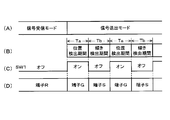
- FIG. 7 is a diagram used to explain the operation of a configuration example of the electronic circuit portion of the electronic pen 100.
- the control circuit 101 sets the electronic pen main body 1 in a signal reception mode for receiving a signal from the position detection sensor of the position detection device in a steady state.
- this signal reception mode after confirming the reception of the signal from the position detection device and performing the predetermined processing described above, the mode is switched to the signal transmission mode in which the signal is transmitted to the position detection device.
- the switch circuit 104 in the signal reception mode, the switch circuit 104 is turned off by the control signal SW1 (see FIG. 7C) from the control circuit 101, and the changeover switch circuit 105 is a movable terminal by the changeover control signal SW2. M is controlled to be connected to the terminal R (see FIG. 7 (D)).
- the signal from the position detection device received by the peripheral electrode 13 is supplied to the signal reception circuit 103 through the changeover switch circuit 105 and demodulated, and the demodulated received signal is the control circuit 101. Is supplied to.
- the control circuit 101 analyzes the received signal from the position detection device to determine the specifications of the other position detection device.
- the received signal from the position detection device includes information instructing the timing when the electronic pen main body 1 starts transmitting the signal. Therefore, based on the information instructing the timing, the control circuit 101 determines the switching timing from the signal reception mode to the signal transmission mode, and also determines the timing of the time division processing in the signal transmission mode. To do. After that, the control circuit 101 switches the electronic pen main body 1 from the signal reception mode to the signal transmission mode.
- the tilt detection period Tb for detecting the tilt angle of 100 is executed in a time division manner.
- the switch circuit 104 is turned on by the control signal SW1 (see FIG. 7C), and the movable terminal M of the changeover switch circuit 105 is connected to the terminal G by the changeover control signal SW2. (See FIG. 7 (D)). Therefore, during the position detection period Ta, the peripheral electrode 13 is connected to the ground electrode through the changeover switch circuit 105. Then, the control circuit 101 controls the signal transmission circuit 102 so as to output the burst signal of the position detection signal and the pen pressure information during the position detection period Ta. The position detection signal and pen pressure information output from the signal transmission circuit 102 are supplied to the core 15 through the switch circuit 104 and sent to the position detection sensor. In this case, the control circuit 101 controls the signal transmission circuit 102 so that the pen pressure information is transmitted from the core body 15 after the burst signal transmission period ends.
- the peripheral electrode 13 is connected to the ground electrode, the core body 15 is shielded except for the tip portion 15a which is the pen tip thereof. Therefore, the signal from the signal transmission circuit 102 is transmitted from the tip portion 15a of the core body 15 without being affected by the outside.
- the switch circuit 104 is turned off by the control signal SW1 (see FIG. 7C), and the changeover switch circuit 105 has the movable terminal M as the terminal S by the changeover control signal SW2. (See FIG. 7 (D)).
- the control circuit 101 controls the signal transmission circuit 102 so as to generate a burst signal for inclination detection.
- the burst signal for tilt detection is a signal having the same frequency as the burst signal of the position detection signal.
- the burst signal for tilt detection from the signal transmission circuit 102 is supplied to the peripheral electrode 13 through the changeover switch circuit 105 and sent to the position detection sensor.
- the position detection device that receives the burst signal for tilt detection through the position detection sensor detects the tilt angle of the electronic pen 100 as described later.
- FIG. 8 is a diagram for explaining the detection of the tilt angle of the electronic pen 100 performed on the position detecting device side based on the signal from the electronic pen 100 of the embodiment.
- the electrostatically coupled region OBa is a perfect circular region as shown in FIG. 8 (B).
- the peripheral electrode 13 and the position detection sensor 200 are electrostatically coupled, and the electrostatically coupled region OBb is a ring-shaped region as shown in FIG. 8C. ..
- the core body 15 of the electronic pen main body 1 of the electronic pen 100 is tilted with respect to the input surface of the position detection sensor 200.
- the region OBa that electrostatically couples between the tip portion 15a of the core body 15 and the position detection sensor 200 during the position detection period Ta remains a substantially perfect circular region as shown in FIG. 8 (E).
- the region OBb that electrostatically couples between the peripheral electrode 13 and the position detection sensor 200 is an ellipse that corresponds to the tilt angle and extends long in the tilt direction, as shown in FIG. 8 (F). It becomes the area of the shape.
- the control circuit of the position detection device can detect the magnitude of the tilt angle of the electronic pen 100 from the elliptical length of the region OBb shown in FIG. 8 (F) in the oval direction. Further, the direction of inclination of the electronic pen 100 can be detected by detecting the elliptical elliptical direction of the region OBb starting from the designated position of the electronic pen 100 shown in FIG. 8 (E).
- the peripheral electrode 13 used to detect the tilt angle may use a signal having the same frequency as the signal supplied to the core body 15, but the frequency of the signal supplied to the core body 15 may be used. , The frequency of the signal supplied to the peripheral electrode 13 may be different. In that case, the position detection device can distinguish between the signal from the core body 15 and the signal from the peripheral electrode 13.
- the position detection period Ta and the inclination detection period Tb are not executed in a time division manner as described above, but the signal from the core body 15 and the peripheral electrode 13 are used.
- the signal may be configured to be simultaneously transmitted to the position detection sensor 200.
- the position detection device can process the electronic pen 100 to simultaneously detect the indicated position and the inclination of the electronic pen 100.
- control circuit 101 and the connector portion 3 are electrically connected. This indicates that information such as data and programs can be transmitted and received to and from an external device through the connector unit 3.
- control circuit 101 is configured as a so-called microprocessor composed of, for example, a CPU (Central Processing unit), a ROM (Read only Memory), a RAM (Random Access Memory) non-volatile memory, and the like.
- various setting information and the like are provided by an external device, a program for operating the electronic pen is provided, and pen pressure information stored in the electronic pen 100 is supplied to the external device. You will be able to provide things such as.
- the electronic pen 100 of the above-described embodiment can be made thinner by providing the connector portion in the connector housing 4 having a substantially triangular cross section.
- the connector housing 4 having a substantially triangular cross section.
- the axis of the electronic pen 100 passes through the axis of the electronic pen body 1 and the axis of the connector substrate 31. It can be configured to pass through the heart. This makes it possible to construct an electronic pen that is strong against the pressure applied from the pen tip direction to the rear end side and is also strong against the pressure applied from the rear end side to the pen tip side.
- connection configuration between the core 15 and the circuit board of the electronic pen body 1 and the connection configuration between the connector board 31 and the electronic pen is not complicated. That is, even if the connector portion is provided, the configuration can be prevented from becoming particularly complicated as compared with the conventional electronic pen.
- the peripheral electrode 13 is used for detecting the tilt angle of the electronic pen 100, but the present invention is not limited to this.
- the peripheral electrode 13 can function as a shield electrode that prevents noise from being mixed into the core body 15.
- the electronic pen housing 2 has been described as having a substantially triangular cross section like the connector housing 4, but the present invention is not limited to this.
- the electronic pen housing 2 may have any cross-sectional shape as long as it can accommodate the electronic pen main body 1. However, if the cross-sectional shape of the electronic pen housing 2 and the cross-sectional shape of the connector housing 4 are matched as in the above-described embodiment, the electronic pen has no step on the side surface even when both are connected. Can be configured.
- the present invention is not limited to this.
- an EMR type electronic pen it may be necessary to send / receive data or a program in order to improve the functionality.
- a short-range wireless communication function of the Bluetooth (registered trademark) standard may be installed. In such a case, the power supply voltage is supplied. It may be necessary to install a battery for this purpose and charge it.
- the present invention can be applied to an EMR type electronic pen, and a connector portion can be provided at the rear end portion of the electronic pen.
- Control circuit 102 ... Signal transmission circuit, 103 ... Signal reception circuit, 104 ... Switch circuit, 105 ... Changeover switch circuit, 106 ... Charging circuit, 107 ... Battery, 5C ... Variable capacitance capacitor, 5R ... Resistance
Abstract
Provided is an electronic pen which can have an uncomplicated structure even if a connector part is provided, and which has sufficient strength to address a writing pressure and a load applied during insertion/removal of a plug and further achieves thinness. At least a connector housing (4) has a substantially triangular cross-section in a direction orthogonal to the axial direction. An electronic pen housing has an electronic pen body part (1) housed therein, and the connector housing (4) has a connector part (3) housed therein. The connector part (3) includes: a connector substrate (31); and a terminal section (32) comprising a base portion and a contact portion. In a state where the connector housing (4) is attached to the electronic pen housing, the axis of the connector substrate (31) coincides with the axis of the electronic pen body part (1).
Description
この発明は、位置検出装置を通じて情報の入力を行うようにするための電子ペンに関する。
The present invention relates to an electronic pen for inputting information through a position detecting device.
位置検出装置のセンサ部に対して信号を送信するために、電池駆動の電子ペンが利用されている。電子ペンに充電式電池が搭載されている場合には、当該充電式電池に充電するためのコネクタを設ける必要がある。また、近年においては、電子ペンの高機能化のために、電子ペンと例えばパーソナルコンピュータなどの外部機器との間でデータやプログラムの送受を行う必要が生じる場合もあり、データの送受信用のコネクタを設ける必要も生じてきている。
A battery-powered electronic pen is used to transmit a signal to the sensor unit of the position detection device. When the electronic pen is equipped with a rechargeable battery, it is necessary to provide a connector for charging the rechargeable battery. Further, in recent years, in order to improve the functionality of the electronic pen, it may be necessary to send and receive data and programs between the electronic pen and an external device such as a personal computer, and a connector for transmitting and receiving data. There is also a need to provide.
このような場合に対応するため、後に記す特許文献1には、電子ペンの筒状筐体の後端側に、後端面からUSB(Universal Serial Bus)規格のプラグを挿抜可能なように、コネクタを配置した電子ペンに関する発明が開示されている。特許文献1に記載の発明は、電子ペンの円形後端面の直径上を中心に、USB規格のコネクタを設けるようにするものであり、当該コネクタ部が電子ペンの使用の邪魔になることが無く、プラグの挿抜も適切に行うことができる。
In order to deal with such a case, Patent Document 1 described later describes a connector on the rear end side of the tubular housing of the electronic pen so that a USB (Universal Serial Bus) standard plug can be inserted and removed from the rear end surface. The invention relating to the electronic pen in which the above is arranged is disclosed. The invention described in Patent Document 1 is to provide a USB standard connector centered on the diameter of the circular rear end surface of the electronic pen, and the connector portion does not interfere with the use of the electronic pen. , The plug can be inserted and removed properly.
一般に、コネクタ部は、特許文献1にも開示されているように、複数の端子が設けられたコンタクト部とこのコンタクト部を中空に保持するための基台部とからなるハウジングを、金属製のシェル部で覆って構成される。シェル部はコネクタ部分の外郭を構成するもので、ハウジングを確実に保持及び保護し、プラグの嵌合時の位置を決めるための部材である。このようにハウジングやシェル部からなるコネクタ部を電子ペンに搭載する場合、電子ペンの細型化は難しくなる。
Generally, as disclosed in Patent Document 1, the connector portion is made of metal and has a housing including a contact portion provided with a plurality of terminals and a base portion for holding the contact portion in a hollow shape. It is composed by covering with a shell part. The shell portion constitutes the outer shell of the connector portion, and is a member for securely holding and protecting the housing and determining the position when the plug is fitted. When the connector portion including the housing and the shell portion is mounted on the electronic pen in this way, it becomes difficult to make the electronic pen thinner.
また、特許文献1の図1にも示されているように、コネクタ部を回路基板上に設けるために、芯体部分も回路基板の軸心からずれた位置に設ける構成となる。このため、コネクタ部分だけでなく、ペン先側と回路基板との接続部分の構成も複雑になることが考えられる。また、この場合、電子ペンの軸心と、回路基板の軸心とが一致しない構成となり、芯体に係る筆圧やコネクタ部へのプラグの装着時に係る圧力により、回路基板にかかる負荷が大きくなる心配がある。
Further, as shown in FIG. 1 of Patent Document 1, in order to provide the connector portion on the circuit board, the core portion is also provided at a position deviated from the axis of the circuit board. Therefore, not only the connector portion but also the configuration of the connection portion between the pen tip side and the circuit board may be complicated. Further, in this case, the axis of the electronic pen and the axis of the circuit board do not match, and the load applied to the circuit board is large due to the writing pressure on the core and the pressure when the plug is attached to the connector. I'm worried about becoming.
以上のことに鑑み、この発明は、コネクタ部を設けても、構成が複雑になることがなき、筆圧やプラグの挿抜時にかかる負荷にも充分に対応できる強度を備え、更に細型化をも実現する電子ペンを提供することを目的とする。
In view of the above, the present invention does not complicate the configuration even if the connector portion is provided, has sufficient strength to withstand the pen pressure and the load applied when inserting and removing the plug, and further reduces the size. The purpose is to provide an electronic pen that can be realized.
上記課題を解決するため、
電子ペン本体部と、
前記電子ペン本体部を収納する筒状体である電子ペン筐体と、
コネクタ基板と、前記コネクタ基板から軸心方向と交差する方向に立ち上がった基台部とこの基台部の後端面の前記コネクタ基板から離隔した位置から後端側に延伸されたコンタクト部とからなる端子部とを備えたコネクタ部と、
前記コネクタ部を収納し、前記電子ペン筐体の後端側に接続される筒状体であって、軸心方向と直交する方向の断面が略三角形状となるコネクタ筐体と
を備え、
前記コネクタ部が収納された前記コネクタ筐体を、前記電子ペン本体部が収納された前記電子ペン筐体に取り付けた場合に、前記コネクタ基板の軸心が、前記電子ペン本体部の軸心と一致する
ことを特徴とする電子ペンを提供する。 To solve the above problems
With the main body of the electronic pen
An electronic pen housing that is a tubular body that houses the electronic pen body,
It consists of a connector board, a base portion that rises from the connector board in a direction intersecting the axial direction, and a contact portion that extends from a position separated from the connector board on the rear end surface of the base portion to the rear end side. A connector part with a terminal part and
A tubular body that houses the connector portion and is connected to the rear end side of the electronic pen housing, and includes a connector housing having a substantially triangular cross section in a direction orthogonal to the axial direction.
When the connector housing in which the connector portion is housed is attached to the electronic pen housing in which the electronic pen main body is housed, the axis of the connector board becomes the axis of the electronic pen body. Provide an electronic pen characterized by matching.
この電子ペンによれば、電子ペン筐体とコネクタ筐体とは、相互に接続されるものであり、共に筒状体であるが、少なくともコネクタ筐体は、軸心方向と直交する方向の断面が、略三角形状とされたものである。電子ペン筐体には電子ペン本体部が収納され、コネクタ筐体にはコネクタ基板と、コネクタ基板から立ち上がった基台部及び基台部の後端面のコネクタ基板から離隔した意位から延伸されたコンタクト部からなる端子部とにより構成されるコネクタ部が収納される。従って、端子部のコンタクト部はコネクタ基板の軸心からは偏心した位置に形成される。
According to this electronic pen, the electronic pen housing and the connector housing are connected to each other and both are tubular bodies, but at least the connector housing has a cross section in a direction orthogonal to the axial direction. However, it has a substantially triangular shape. The electronic pen main body is housed in the electronic pen housing, and the connector housing is extended from a position separated from the connector board, the base portion rising from the connector board, and the connector board on the rear end surface of the base portion. A connector portion composed of a terminal portion composed of a contact portion is housed. Therefore, the contact portion of the terminal portion is formed at a position eccentric from the axial center of the connector substrate.
これにより、端子部のコンタクト部をコネクタ筐体の軸心方向と直交する方向の略三角形状の断面の底辺側の領域に形成することが可能になる。しかも、電子ペン筐体にコネクタ筐体が取り付けられ状態になると、前記コネクタ基板の軸心が、前記電子ペン本体部の軸心と一致するようにされる。当該構成により、従来からの電子ペンの場合と同様に、電子ペン本体部の軸心上に電子ペンの重要な構成部分を配置することできる。これにより、コネクタ部を設けても、従来の電子ペンに比べて構成が複雑になることが無く、筆圧による負荷やプラグの挿抜による負荷にも充分に対応できる強度を備え、更に細型化をも実現した電子ペンが構成される。
This makes it possible to form the contact portion of the terminal portion in the region on the bottom side of the substantially triangular cross section in the direction orthogonal to the axial direction of the connector housing. Moreover, when the connector housing is attached to the electronic pen housing, the axis of the connector board is made to coincide with the axis of the electronic pen main body. With this configuration, an important component of the electronic pen can be arranged on the axis of the main body of the electronic pen, as in the case of the conventional electronic pen. As a result, even if the connector part is provided, the configuration will not be complicated compared to the conventional electronic pen, and it will have sufficient strength to withstand the load due to writing pressure and the load due to plug insertion and removal, and further slimming down. An electronic pen that has also been realized is constructed.
以下、図を参照しながら、この発明の電子ペンの実施の形態について説明する。近年においては、グラフィックデザインを行うペンタブレットやスマートフォンやタブレットPC(personal Computer)などの電子機器において、位置検出装置と電子ペンからなる入力デバイスが用いられている。これにより、紙にペンで筆記を行う場合と同様にして、電子機器に対して、細かな描画入力や文字入力を行うことができる。電子ペン及び位置検出装置における位置検出方式には、種々の方式があるが、代表的なものには、例えば、電磁結合方式や静電容量方式がある。
Hereinafter, embodiments of the electronic pen of the present invention will be described with reference to the drawings. In recent years, input devices including a position detection device and an electronic pen have been used in electronic devices such as pen tablets, smartphones, and tablet PCs (personal computers) that perform graphic design. As a result, it is possible to perform detailed drawing input and character input to the electronic device in the same manner as when writing on paper with a pen. There are various position detection methods in the electronic pen and the position detection device, and typical ones include, for example, an electromagnetic coupling method and a capacitance method.
電磁誘導方式は、X軸方向とY軸方向とのそれぞれに複数のループコイルを配設したセンサ部を位置検出装置が備える。そして、当該センサ部の複数のループコイルに順次に電力を供給して磁界を発生させる送信期間と、電力の供給を停止し外部からの磁界を受信する受信期間とを交互に設ける。対応する電子ペンは、コイルとコンデンサとからなる共振回路を備え、当該センサ部からの磁界に応じて、当該コイルに電流が流れることにより信号を発生させ、この信号に筆圧情報を含めて位置検出センサに送信する。これを受信期間において位置検出装置が受信して、電子ペンによる指示位置と筆圧を検出する。
In the electromagnetic induction method, the position detection device includes a sensor unit in which a plurality of loop coils are arranged in each of the X-axis direction and the Y-axis direction. Then, a transmission period in which electric power is sequentially supplied to the plurality of loop coils of the sensor unit to generate a magnetic field and a reception period in which the supply of electric power is stopped and a magnetic field from the outside is received are alternately provided. The corresponding electronic pen is provided with a resonance circuit consisting of a coil and a capacitor, and a signal is generated by a current flowing through the coil in response to a magnetic field from the sensor unit, and the position including the pen pressure information in this signal. Send to the detection sensor. This is received by the position detection device during the reception period, and the position indicated by the electronic pen and the writing pressure are detected.
静電容量方式は、X軸方向とY軸方向とのそれぞれに複数の線状導体(ライン電極)を配設したセンサ部を位置検出装置が備える。そして、当該センサ部は、指や静電ペンが近づけられることによって、線状導体に生じる静電容量(電荷)の変化に応じて指示位置を検出する。なお、静電ペンには、導電性を有するペン型の位置指示器、あるいはバッテリで駆動され、信号を送出するいわゆるアクティブ静電ペンがある。アクティブ静電ペンを用いるアクティブ静電結合方式の場合には、電子ペンは、電子ペンに搭載された発振回路からの信号に筆圧情報をも含めて送信し、これを位置検出装置で受信して、指示位置と筆圧を検出する。
In the capacitance method, the position detection device includes a sensor unit in which a plurality of linear conductors (line electrodes) are arranged in each of the X-axis direction and the Y-axis direction. Then, the sensor unit detects the indicated position according to the change in the capacitance (charge) generated in the linear conductor when the finger or the electrostatic pen is brought close to the sensor unit. The electrostatic pen includes a pen-type position indicator having conductivity or a so-called active electrostatic pen driven by a battery and transmitting a signal. In the case of the active electrostatic coupling method using an active electrostatic pen, the electronic pen transmits the signal from the oscillation circuit mounted on the electronic pen including the pen pressure information, and receives this by the position detection device. The indicated position and pen pressure are detected.
この出願の発明の電子ペンは、種々の方式の電子ペン適用可能である。従って、この出願の発明の電子ペンは、上述の電磁誘導方式の電子ペンにも、また、アクティブ静電結合方式の電子ペン(アクティブ静電ペン)にも適用可能なものである。以下に説明する実施の形態においては、説明を明確に行うため、アクティブ静電結合方式(AES(Active Electrostatic)方式)の電子ペンに、この発明の電子ペンを適用した場合を例にして説明する。
The electronic pen of the invention of this application can be applied to various types of electronic pens. Therefore, the electronic pen of the invention of the present application is applicable to the above-mentioned electromagnetic induction type electronic pen and also to the active electrostatic coupling type electronic pen (active electrostatic pen). In the embodiment described below, in order to clarify the description, a case where the electronic pen of the present invention is applied to an electronic pen of an active electrostatic coupling method (AES (Active Electrostatic) method) will be described as an example. ..
[電子ペン100の全体構成]
図1は、この実施の形態の電子ペン100の全体構成を説明するための分解斜視図である。この実施の形態の電子ペン100は、図1に示すように、電子ペン本体部1と、電子ペン本体部1を収納する筒状体であって、軸心方向と直交する方向の断面が略三角形状となる電子ペン筐体2を備える。さらに、電子ペン本体部1の後端には、後述するコネクタ部を収納し、電子ペン筐体2の後端側に接続される筒状体であって、軸心方向と直交する方向の断面が、電子ペン筐体2の断面と合致するコネクタ筐体4が設けられる。つまり、コネクタ筐体4は、電子ペン筐体2の断面と同じ略三角形状の断面を備えるものである。従って、電子ペン筐体2に対して、コネクタ筐体4を接続した場合には、これらの筐体間に段差を生じさせることなく、1本の電子ペン100を構成することができる。 [Overall configuration of electronic pen 100]
FIG. 1 is an exploded perspective view for explaining the overall configuration of the electronic pen 100 of this embodiment. As shown in FIG. 1, the electronic pen 100 of this embodiment is a tubular body that houses the electronic penmain body 1 and the electronic pen main body 1, and has a substantially cross section in a direction orthogonal to the axial direction. The electronic pen housing 2 having a triangular shape is provided. Further, the rear end of the electronic pen main body 1 houses a connector portion described later, and is a tubular body connected to the rear end side of the electronic pen housing 2 and has a cross section in a direction orthogonal to the axial direction. However, a connector housing 4 that matches the cross section of the electronic pen housing 2 is provided. That is, the connector housing 4 has a substantially triangular cross section which is the same as the cross section of the electronic pen housing 2. Therefore, when the connector housing 4 is connected to the electronic pen housing 2, one electronic pen 100 can be configured without causing a step between the housings.
図1は、この実施の形態の電子ペン100の全体構成を説明するための分解斜視図である。この実施の形態の電子ペン100は、図1に示すように、電子ペン本体部1と、電子ペン本体部1を収納する筒状体であって、軸心方向と直交する方向の断面が略三角形状となる電子ペン筐体2を備える。さらに、電子ペン本体部1の後端には、後述するコネクタ部を収納し、電子ペン筐体2の後端側に接続される筒状体であって、軸心方向と直交する方向の断面が、電子ペン筐体2の断面と合致するコネクタ筐体4が設けられる。つまり、コネクタ筐体4は、電子ペン筐体2の断面と同じ略三角形状の断面を備えるものである。従って、電子ペン筐体2に対して、コネクタ筐体4を接続した場合には、これらの筐体間に段差を生じさせることなく、1本の電子ペン100を構成することができる。 [Overall configuration of electronic pen 100]
FIG. 1 is an exploded perspective view for explaining the overall configuration of the electronic pen 100 of this embodiment. As shown in FIG. 1, the electronic pen 100 of this embodiment is a tubular body that houses the electronic pen
電子ペン本体部1は、例えば金属材料により形成されたパイプ部11を備える。パイプ部11の内部には、詳しくは後述する電子回路が搭載された回路基板や中心電極を構成する芯体などといった、電子ペン機能を実現するための主要部品が収納される。パイプ部11のペン先(先端)側には、プラスチックなどの樹脂材料(絶縁材料)により形成されたリンク状の結合部材12を介して、例えば金属などの導電性材料で形成された筒状の周辺電極13が連結される。
The electronic pen main body 1 includes, for example, a pipe portion 11 made of a metal material. Inside the pipe portion 11, main parts for realizing the electronic pen function, such as a circuit board on which an electronic circuit described later is mounted and a core body constituting a center electrode, are housed. On the pen tip (tip) side of the pipe portion 11, a tubular shape formed of a conductive material such as metal via a link-shaped coupling member 12 formed of a resin material (insulating material) such as plastic. Peripheral electrodes 13 are connected.
周辺電極13は、パイプ部11と同じ外径を有する筒状部13bと、先細となったテーパー部13aとの2つの部分が、一体的に形成されたものである。周辺電極13の先端部には、例えばブラスチックなどの樹脂材料(絶縁材料)により形成されたリング状のフロントキャップ14が設けられる。このフロントキャップ14の開口より、例えば導電性ポリアセタール樹脂などの導電性材料により形成された芯体(中心電極)15の先端部分が突出し、ペン先を構成する。また、電子ペン本体部1のパイプ部11側面には、この実施の形態では2つのサイドスイッチが設けられたサイドスイッチ部16が設けられる。
The peripheral electrode 13 is formed by integrally forming two portions, a tubular portion 13b having the same outer diameter as the pipe portion 11 and a tapered portion 13a. A ring-shaped front cap 14 formed of a resin material (insulating material) such as plastic is provided at the tip of the peripheral electrode 13. From the opening of the front cap 14, the tip portion of the core body (center electrode) 15 formed of a conductive material such as a conductive polyacetal resin protrudes to form a pen tip. Further, on the side surface of the pipe portion 11 of the electronic pen main body portion 1, a side switch portion 16 provided with two side switches is provided in this embodiment.
電子ペン本体部1が収納される電子ペン筐体2は、例えば、プラスチックなどの樹脂材料により形成されたパイプ状のものであり、ペン先(先端)側が先細(テーパー形状)になったものである。なお、電子ペン筐体2は、例えば、木製などといった樹脂以外の非導電性材料によって形成することもできる。電子ペン筐体2の側面には、サイドスイッチ用の孔部21A、21Bが設けられている。これらの孔部21A、21Bは、電子ペン筐体2に収納された電子ペン本体部1のサイドスイッチ部16にある2のサイドスイッチの各々に対応する位置に設けられている。
The electronic pen housing 2 in which the electronic pen main body 1 is housed is, for example, a pipe-shaped one made of a resin material such as plastic, and the pen tip (tip) side is tapered (tapered). is there. The electronic pen housing 2 can also be formed of a non-conductive material other than resin, such as wood. Holes 21A and 21B for side switches are provided on the side surface of the electronic pen housing 2. These holes 21A and 21B are provided at positions corresponding to each of the two side switches in the side switch portion 16 of the electronic pen main body 1 housed in the electronic pen housing 2.
これらのサイドスイッチ用の孔部21A、21Bには、例えばプラスチックなどの樹脂により形成された操作ボタン22A、22Bが嵌め込まれる。操作ボタン22A、22Bは、押圧することにより電子ペン筐体2の内側に押し込まれ、押圧を解除すれば押圧前の位置に復帰する構成になっている。これにより、操作ボタン22A、22Bを介して、電子ペン本体部1に設けられているサイドスイッチを押下操作することができる。なお、電子ペンにおけるサイドスイッチは、パーソナルコンピュータのポインティングデバイスであるいわゆるマウスの左クリックボタンや右クリックボタンに相当する。従って、サイドスイッチを操作することにより、位置検出装置が搭載されたペンタブレットなどの電子機器において、例えば、ウィンドウメニューを表示して、目的とする項目を選択したりするなどのことができる。
Operation buttons 22A and 22B made of resin such as plastic are fitted into the holes 21A and 21B for these side switches. The operation buttons 22A and 22B are pushed into the electronic pen housing 2 by pressing, and return to the position before pressing when the pressing is released. As a result, the side switch provided on the electronic pen main body 1 can be pressed via the operation buttons 22A and 22B. The side switch in the electronic pen corresponds to a so-called left-click button or right-click button of a mouse, which is a pointing device of a personal computer. Therefore, by operating the side switch, in an electronic device such as a pen tablet equipped with a position detection device, for example, a window menu can be displayed and a target item can be selected.
電子ペン本体部1の後端側に設けられるコネクタ筐体4は、例えばプラスチックなどの樹脂材料により形成されたボディ部41と、金属材料により形成されたエンドキャップ42とからなる。ボディ部41とエンドキャップ42とは、断面形状は同じであり、図1に示したように、これらを接続しても段差が生じることはない。このような外観を有するコネクタ筐体4の内部は中空になっており、後述するコネクタ部が搭載される。
The connector housing 4 provided on the rear end side of the electronic pen main body 1 is composed of a body 41 made of a resin material such as plastic and an end cap 42 made of a metal material. The body portion 41 and the end cap 42 have the same cross-sectional shape, and as shown in FIG. 1, no step is generated even if they are connected. The inside of the connector housing 4 having such an appearance is hollow, and a connector portion described later is mounted on the connector housing 4.
図2は、実施の形態の電子ペンの電子ペン本体部1とコネクタ筐体4の外観について説明するための図である。図2(A)に示すように、電子ペン本体部1とコネクタ筐体4とは相互に接続される。具体的には、電子ペン本体部1のパイプ部11に搭載された回路基板と、コネクタ筐体4に搭載された後述するコネクタ基板とが電気的に接続され、更に、両基板同士が固着される。この場合の接続方法は、種々の方法を用いることができる。一例を挙げれば、電子ペン本体部1のパイプ部11に搭載された回路基板の後端部にジャック(受け口)型の接続部を設け、コネクタ筐体4に搭載されたコネクタ基板の先端部にプラグ(差し口)型の接続部を設ける。これにより、両者を接続することにより、電気的にも接続され、また、物理的にも固着されるようにできる。
FIG. 2 is a diagram for explaining the appearance of the electronic pen main body 1 and the connector housing 4 of the electronic pen of the embodiment. As shown in FIG. 2A, the electronic pen main body 1 and the connector housing 4 are connected to each other. Specifically, the circuit board mounted on the pipe portion 11 of the electronic pen main body 1 and the connector board mounted on the connector housing 4 to be described later are electrically connected, and both boards are further fixed to each other. To. As the connection method in this case, various methods can be used. For example, a jack (receptacle) type connection portion is provided at the rear end portion of the circuit board mounted on the pipe portion 11 of the electronic pen main body portion 1, and the tip portion of the connector board mounted on the connector housing 4 is provided. Provide a plug (outlet) type connection. As a result, by connecting the two, they can be electrically connected and physically fixed.
コネクタ筐体4の後端部のエンドキャップ42の後端面には、図2(B)に示すように、コネクタ筐体4に搭載されるコネクタ部のコンタクト部に対して、対応するプラグを挿抜するための開口部42Hが設けられる。図2(B)においては、開口部42Hより、コネクタ筐体4に搭載されたコネクタ部の端子部を構成する基台部32Aとコンタクト部32Bとが見える状態を示している。
As shown in FIG. 2B, a corresponding plug is inserted into and removed from the contact portion of the connector portion mounted on the connector housing 4 on the rear end surface of the end cap 42 at the rear end portion of the connector housing 4. An opening 42H is provided for this purpose. FIG. 2B shows a state in which the base portion 32A and the contact portion 32B constituting the terminal portion of the connector portion mounted on the connector housing 4 can be seen from the opening 42H.
[コネクタ部の構成例]
図3は、実施の形態の電子ペンのコネクタ部の詳細を説明するための図である。図3(A)は、コネクタ筐体4部分を、その後端面側から見た場合の斜視図である。ボディ部41とエンドキャップ42とからなるコネクタ筐体4の軸心方向と交差する方向の断面形状は、エンドキャップ42の後端面が示すように、略三角形状であり、当該後端面には、プラグの挿抜のための開口部42Hが設けられている。この開口部42Hの奥には、コネクタ部3が搭載されている。すなわち、コネクタ筐体4には、コネクタプラグ(挿し口)が差し込まれるジャック部(受け口)が構成される。 [Configuration example of connector part]
FIG. 3 is a diagram for explaining the details of the connector portion of the electronic pen of the embodiment. FIG. 3A is a perspective view of theconnector housing 4 portion as viewed from the rear end surface side. As shown by the rear end surface of the end cap 42, the cross-sectional shape of the connector housing 4 including the body portion 41 and the end cap 42 in the direction intersecting the axial direction is substantially triangular. An opening 42H for inserting and removing the plug is provided. A connector portion 3 is mounted in the back of the opening 42H. That is, the connector housing 4 is configured with a jack portion (receptacle) into which the connector plug (insertion port) is inserted.
図3は、実施の形態の電子ペンのコネクタ部の詳細を説明するための図である。図3(A)は、コネクタ筐体4部分を、その後端面側から見た場合の斜視図である。ボディ部41とエンドキャップ42とからなるコネクタ筐体4の軸心方向と交差する方向の断面形状は、エンドキャップ42の後端面が示すように、略三角形状であり、当該後端面には、プラグの挿抜のための開口部42Hが設けられている。この開口部42Hの奥には、コネクタ部3が搭載されている。すなわち、コネクタ筐体4には、コネクタプラグ(挿し口)が差し込まれるジャック部(受け口)が構成される。 [Configuration example of connector part]
FIG. 3 is a diagram for explaining the details of the connector portion of the electronic pen of the embodiment. FIG. 3A is a perspective view of the
コネクタ部3は、図3(B)のコネクタ部の斜視図に示すように、コネクタ基板31と端子部32とから構成される。端子部32は、コネクタ基板31の後端側において、軸心方向Jと交差する方向に立ち上がった基台部32Aと、この基台部32Aの後端面のコネクタ基板から離隔した位置より軸心方向Jに沿って後端側に延伸されたコンタクト部32Bとからなる。このように、端子部32は、基台部32Aとコンタクト部32Bとによって構成され、コネクタ基板31の軸心から偏心した位置にコンタクト部32Bが位置するようになっている。
As shown in the perspective view of the connector portion of FIG. 3B, the connector portion 3 is composed of a connector board 31 and a terminal portion 32. The terminal portion 32 is located on the rear end side of the connector board 31 in the axial direction from a position separated from the base portion 32A that rises in the direction intersecting the axial direction J and the rear end surface of the base portion 32A. It is composed of a contact portion 32B extending toward the rear end side along J. As described above, the terminal portion 32 is composed of the base portion 32A and the contact portion 32B, and the contact portion 32B is located at a position eccentric from the axial center of the connector substrate 31.
すなわち、図3(C)のコネクタ部3が搭載されたコネクタ筐体4部分の断面図に示すように、コネクタ筐体4のエンドキャップ42部分に、コネクタ基板31と端子部32とからなるコネクタ部3が挿入されて固定される。この場合、開口部42Hの中央部分にコンタクト部32Bが位置するようにされる。エンドキャップ42は、金属材料により形成されたものであり、コネクタ部3のシェル部の機能を実現する。すなわち、エンドキャップ42は、コネクタ部3の外郭を構成し、コネクタ部3を確実に保持及び保護し、プラグの嵌合時の位置を規制することができる。また、エンドキャップ42は、金属材料により形成されているので、外部からのノイズの混入を防止する機能をも備える。このように、コネクタ筐体4とコネクタ部3とによって、電子ペン100のコネクタを構成する。
That is, as shown in the cross-sectional view of the connector housing 4 portion on which the connector portion 3 of FIG. 3C is mounted, the end cap 42 portion of the connector housing 4 has a connector composed of the connector board 31 and the terminal portion 32. The part 3 is inserted and fixed. In this case, the contact portion 32B is positioned at the central portion of the opening 42H. The end cap 42 is made of a metal material and realizes the function of the shell portion of the connector portion 3. That is, the end cap 42 constitutes the outer shell of the connector portion 3, securely holds and protects the connector portion 3, and can regulate the position when the plug is fitted. Further, since the end cap 42 is made of a metal material, it also has a function of preventing noise from being mixed in from the outside. In this way, the connector housing 4 and the connector portion 3 form a connector for the electronic pen 100.
なお、図3(C)においては、コネクタ部3のコネクタ基板31の前端部と、電子ペン本体部1のパイプ部11に搭載された回路基板1Cの後端部とが接続された状態を示しているが、電子ペン本体部1とコネクタ部3との位置関係が重要である。
Note that FIG. 3C shows a state in which the front end portion of the connector board 31 of the connector portion 3 and the rear end portion of the circuit board 1C mounted on the pipe portion 11 of the electronic pen main body 1 are connected. However, the positional relationship between the electronic pen main body 1 and the connector 3 is important.
[電子ペン本体部とコネクタ部の位置関係]
図4は、実施の形態の電子ペン100の電子ペン本体部1とコネクタ部3との位置関係について説明するための図である。図4(A)は、電子ペン本体部1に設けられたサイドスイッチ部16その側面方向から見た場合の図であり、図4(B)は、電子ペン本体部1に設けられたサイドスイッチ部16その上面方向から見た場合の図である。図4においては、電子ペン本体部1とコネクタ筐体4内に設けられているコネクタ部3とを接続した場合を示している。すなわち、図4は、電子ペン本体部1に搭載された回路基板とコネクタ筐体4に搭載されたコネクタ基板31とが接続された状態になっている。 [Positional relationship between the electronic pen body and the connector]
FIG. 4 is a diagram for explaining the positional relationship between the electronic penmain body 1 and the connector 3 of the electronic pen 100 of the embodiment. FIG. 4A is a view of the side switch portion 16 provided on the electronic pen main body 1 when viewed from the side surface direction thereof, and FIG. 4B is a side switch provided on the electronic pen main body 1. 16 is a view when viewed from the upper surface direction thereof. FIG. 4 shows a case where the electronic pen main body 1 and the connector 3 provided in the connector housing 4 are connected. That is, FIG. 4 shows a state in which the circuit board mounted on the electronic pen main body 1 and the connector board 31 mounted on the connector housing 4 are connected.
図4は、実施の形態の電子ペン100の電子ペン本体部1とコネクタ部3との位置関係について説明するための図である。図4(A)は、電子ペン本体部1に設けられたサイドスイッチ部16その側面方向から見た場合の図であり、図4(B)は、電子ペン本体部1に設けられたサイドスイッチ部16その上面方向から見た場合の図である。図4においては、電子ペン本体部1とコネクタ筐体4内に設けられているコネクタ部3とを接続した場合を示している。すなわち、図4は、電子ペン本体部1に搭載された回路基板とコネクタ筐体4に搭載されたコネクタ基板31とが接続された状態になっている。 [Positional relationship between the electronic pen body and the connector]
FIG. 4 is a diagram for explaining the positional relationship between the electronic pen
図4(A)、(B)を見ると分かるように、どちら側から見ても、電子ペン本体部1の軸心J1と、コネクタ筐体4に搭載されたコネクタ部3のコネクタ基板31の軸心J2とは一致するようにされる。また、この実施の形態においては、図示しないが、電子ペン本体部1のパイプ部11に搭載される回路基板1Cの軸心は、電子ペン本体部1の軸心J1と一致するようにされる。これにより、電子ペン本体部1を搭載した電子ペン筐体2に対して、コネクタ部3を搭載したコネクタ筐体4とを接続した(取り付けた)場合には、コネクタ基板31の軸心J2が、電子ペン本体部1の軸心J1と一致する。
As can be seen from FIGS. 4 (A) and 4 (B), the axis J1 of the electronic pen main body 1 and the connector board 31 of the connector 3 mounted on the connector housing 4 are viewed from either side. It is made to coincide with the axis J2. Further, in this embodiment, although not shown, the axis of the circuit board 1C mounted on the pipe portion 11 of the electronic pen main body 1 is set to coincide with the axial center J1 of the electronic pen main body 1. .. As a result, when the electronic pen housing 2 on which the electronic pen main body 1 is mounted is connected (attached) to the connector housing 4 on which the connector portion 3 is mounted, the axis J2 of the connector board 31 becomes , Consistent with the axis J1 of the electronic pen main body 1.
従って、この実施の形態の電子ペン100の芯体15の先端(ペン先)からエンドキャップ42の後端面に至るまで、電子ペン100の軸心が、電子ペン本体部1の軸心を通り、コネクタ基板31の軸心を通るように構成される。これにより、芯体15の先端に筆圧がかけられても、また、コネクタ部3に外部よりプラグが押し込まれても、掛けられる圧力は、軸心を通じて受け止めることができるので、電子ペン100のいずれかの部分だけに、過度の圧力がかかることが無い。従って、ペン先方向から後端側にかけられる圧力にも強く、後端側からペン先側にかけられる圧力にも強い、電子ペンを構成できる。換言すれば、ペン先方向から後端側にかけられる圧力にも、また、後端側からペン先側にかけられる圧力にも、耐久性の高い電子ペンを構成できる。
Therefore, the axis of the electronic pen 100 passes through the axis of the electronic pen main body 1 from the tip (pen tip) of the core body 15 of the electronic pen 100 of this embodiment to the rear end surface of the end cap 42. It is configured to pass through the axis of the connector board 31. As a result, even if a writing pressure is applied to the tip of the core body 15 or a plug is pushed into the connector portion 3 from the outside, the applied pressure can be received through the axis of the electronic pen 100. Excessive pressure is not applied to only one of the parts. Therefore, it is possible to construct an electronic pen that is strong against the pressure applied from the pen tip direction to the rear end side and is also strong against the pressure applied from the rear end side to the pen tip side. In other words, it is possible to construct an electronic pen having high durability against both the pressure applied from the pen tip direction to the rear end side and the pressure applied from the rear end side to the pen tip side.
また、図4(B)に示すように、コネクタ基板31の横幅は、端子部32(基台部32Aとコンタクト部32Bとからなる部分)の横幅以下にする。これにより、電子ペン100の細型化を阻害することが無いようにできる。つまり、コネクタ基板31の横幅を、端子部32の横幅と同じか、より短くなるように構成すれば、コネクタ筐体4の断面の面積をコネクタ基板31の影響を受けて広くする必要がない。
Further, as shown in FIG. 4B, the width of the connector board 31 is set to be equal to or less than the width of the terminal portion 32 (the portion including the base portion 32A and the contact portion 32B). As a result, it is possible to prevent the electronic pen 100 from being thinned. That is, if the width of the connector board 31 is configured to be the same as or shorter than the width of the terminal portion 32, it is not necessary to increase the cross-sectional area of the connector housing 4 under the influence of the connector board 31.
[コネクタ部の具体例]
なお、この実施の形態のコネクタ部3は、例えば、USB規格のタイプCに対応するものである。もちろん、これに限ることなく、この実施の形態の電子ペン100に設けられるコネクタ部3は、例えば、USB規格の種々のタイプのコネクタとすることができる。この実施の形態の場合には、上述したように、コネクタ筐体4のエンドキャップ42を、シェル部として用いることができるので、コンタクト部を覆うシェル部を別途設ける必要がなく、電子ペンの細型化を実現している。 [Specific example of connector part]
Theconnector portion 3 of this embodiment corresponds to, for example, the USB standard type C. Of course, the present invention is not limited to this, and the connector portion 3 provided in the electronic pen 100 of this embodiment can be, for example, various types of connectors of the USB standard. In the case of this embodiment, as described above, the end cap 42 of the connector housing 4 can be used as the shell portion, so that it is not necessary to separately provide the shell portion that covers the contact portion, and the electronic pen is thin. Has been realized.
なお、この実施の形態のコネクタ部3は、例えば、USB規格のタイプCに対応するものである。もちろん、これに限ることなく、この実施の形態の電子ペン100に設けられるコネクタ部3は、例えば、USB規格の種々のタイプのコネクタとすることができる。この実施の形態の場合には、上述したように、コネクタ筐体4のエンドキャップ42を、シェル部として用いることができるので、コンタクト部を覆うシェル部を別途設ける必要がなく、電子ペンの細型化を実現している。 [Specific example of connector part]
The
また、この実施の形態のコネクタ部3は、USB規格のものに限るものではない。USB規格以外の種々の規格のコネクタに対応可能である。例えば、充電用の電源端子だけを備えたコネクタに対応するように、コネクタ部を構成することも可能である。また、データを送受するための端子だけを備えたコネクタに対応するように、コネクタ部を構成することも可能である。
Further, the connector portion 3 of this embodiment is not limited to the one of the USB standard. It is compatible with connectors of various standards other than the USB standard. For example, it is possible to configure the connector portion so as to correspond to a connector having only a power supply terminal for charging. It is also possible to configure the connector portion so as to correspond to a connector having only terminals for transmitting and receiving data.
[電子ペン100の外観形状]
図5は、実施の形態の電子ペンの外観について説明するための図である。図5に示すように、この実施の形態の電子ペン100は、いわゆる鉛筆に似た外観を有する。この場合、電子ペン筐体2の後端には、コネクタ筐体4を接続することにより、コネクタ接続機能を実現する。また、電子ペン筐体2の先端からは、電子ペン本体部1の周辺電極13のテーパー部13aとフロントキャップ14と芯体15の先端部分とが突出し、AES方式の電子ペン機能を実現する。 [Appearance shape of electronic pen 100]
FIG. 5 is a diagram for explaining the appearance of the electronic pen of the embodiment. As shown in FIG. 5, the electronic pen 100 of this embodiment has an appearance similar to a so-called pencil. In this case, the connector connection function is realized by connecting theconnector housing 4 to the rear end of the electronic pen housing 2. Further, from the tip of the electronic pen housing 2, the tapered portion 13a of the peripheral electrode 13 of the electronic pen main body 1 and the tip portion of the front cap 14 and the core body 15 project to realize the AES type electronic pen function.
図5は、実施の形態の電子ペンの外観について説明するための図である。図5に示すように、この実施の形態の電子ペン100は、いわゆる鉛筆に似た外観を有する。この場合、電子ペン筐体2の後端には、コネクタ筐体4を接続することにより、コネクタ接続機能を実現する。また、電子ペン筐体2の先端からは、電子ペン本体部1の周辺電極13のテーパー部13aとフロントキャップ14と芯体15の先端部分とが突出し、AES方式の電子ペン機能を実現する。 [Appearance shape of electronic pen 100]
FIG. 5 is a diagram for explaining the appearance of the electronic pen of the embodiment. As shown in FIG. 5, the electronic pen 100 of this embodiment has an appearance similar to a so-called pencil. In this case, the connector connection function is realized by connecting the
この実施の形態の電子ペン100の全長(長手方向の長さ)は、例えば、13cm~16cm程度とされ、市販のボールペンやシャープペンシルと同程度かやや短い構成とされる。また、コネクタ筐体4の断面は、図2(B)、図3(A)に示したように、正三角形の頂点部分を丸く形成した略三角形状であり、一辺のおおよその長さは10mm程度とされる。従って、上述したように、エンドキャップ42がシェル部を構成するので、シェル部の横幅が9mmであるUSB規格のタイプCに合致したコネクタ部をコネクタ筐体4に搭載することが可能になる。なお、電子ペン本体部1のパイプ部11の直径は、例えば、4mm~6mm程度とされる。もちろん、ここに示したサイズは一例であり、種々のサイズに調整することが可能である。
The total length (length in the longitudinal direction) of the electronic pen 100 of this embodiment is, for example, about 13 cm to 16 cm, which is about the same as or slightly shorter than a commercially available ballpoint pen or mechanical pencil. Further, as shown in FIGS. 2 (B) and 3 (A), the cross section of the connector housing 4 is a substantially triangular shape in which the apex portion of an equilateral triangle is rounded, and the approximate length of one side is 10 mm. It is said to be a degree. Therefore, as described above, since the end cap 42 constitutes the shell portion, it is possible to mount the connector portion matching the USB standard type C having a width of the shell portion of 9 mm on the connector housing 4. The diameter of the pipe portion 11 of the electronic pen main body portion 1 is, for example, about 4 mm to 6 mm. Of course, the size shown here is an example and can be adjusted to various sizes.
[電子ペン機能を実現する電子回路部分の構成例]
図6は、電子ペン100の電子ペン機能を実現する電子回路部分の構成例について説明するための図である。図6に示す、制御回路101、信号発信回路102、信号受信回路103、スイッチ回路104、切替スイッチ回路105、充電回路106、バッテリ107は、電子ペン本体部1のパイプ部11に搭載された回路基板1Cに構成される回路部分である。制御回路101は、回路基板1Cに載置されているIC(Integrated Circuit)により実現される。また、スイッチ(図6ではSWと記載。)16A、16Bは、サイドスイッチ部16に設けられたサイドスイッチを構成し、操作ボタン22A、22Bを通じて押下操作されるものであり、操作状態が制御回路101に通知されるようになっている。 [Configuration example of electronic circuit part that realizes electronic pen function]
FIG. 6 is a diagram for explaining a configuration example of an electronic circuit portion that realizes the electronic pen function of the electronic pen 100. Thecontrol circuit 101, the signal transmission circuit 102, the signal reception circuit 103, the switch circuit 104, the changeover switch circuit 105, the charging circuit 106, and the battery 107 shown in FIG. 6 are circuits mounted on the pipe portion 11 of the electronic pen main body 1. It is a circuit part configured on the board 1C. The control circuit 101 is realized by an IC (Integrated Circuit) mounted on the circuit board 1C. Further, the switches (described as SW in FIG. 6) 16A and 16B form a side switch provided in the side switch unit 16 and are pressed and operated through the operation buttons 22A and 22B, and the operation state is the control circuit. It is designed to notify 101.
図6は、電子ペン100の電子ペン機能を実現する電子回路部分の構成例について説明するための図である。図6に示す、制御回路101、信号発信回路102、信号受信回路103、スイッチ回路104、切替スイッチ回路105、充電回路106、バッテリ107は、電子ペン本体部1のパイプ部11に搭載された回路基板1Cに構成される回路部分である。制御回路101は、回路基板1Cに載置されているIC(Integrated Circuit)により実現される。また、スイッチ(図6ではSWと記載。)16A、16Bは、サイドスイッチ部16に設けられたサイドスイッチを構成し、操作ボタン22A、22Bを通じて押下操作されるものであり、操作状態が制御回路101に通知されるようになっている。 [Configuration example of electronic circuit part that realizes electronic pen function]
FIG. 6 is a diagram for explaining a configuration example of an electronic circuit portion that realizes the electronic pen function of the electronic pen 100. The
制御回路101に対しては、信号発信回路102と信号受信回路103とが接続されると共に、筆圧検出部を構成する可変容量コンデンサ5Cが接続されている。可変容量コンデンサ5Cは、芯体15により押圧され、この押圧力に応じて容量、すなわち、プラス電極とマイナス電極に帯電する静電容量を変化させることができるものである。可変容量コンデンサ5Cには、並列に抵抗5Rが接続されている。
The signal transmission circuit 102 and the signal reception circuit 103 are connected to the control circuit 101, and the variable capacitance capacitor 5C constituting the pen pressure detection unit is also connected. The variable capacitance capacitor 5C is pressed by the core body 15, and the capacitance, that is, the capacitance charged on the positive electrode and the negative electrode can be changed according to the pressing force. A resistor 5R is connected in parallel to the variable capacitor 5C.
信号発信回路102の信号出力端が、スイッチ回路104を通じて、芯体15に接続されている。また、この例では、信号発信回路102の信号出力端は、切替スイッチ回路105の端子Sに接続されている。切替スイッチ回路105の可動端子Mは、周辺電極13に接続されている。切替スイッチ回路105の端子Rは、信号受信回路103の入力端に接続されている。また、切替スイッチ回路105の端子Gは、アース電極(グランド電極)に接続されている。
The signal output end of the signal transmission circuit 102 is connected to the core body 15 through the switch circuit 104. Further, in this example, the signal output end of the signal transmission circuit 102 is connected to the terminal S of the changeover switch circuit 105. The movable terminal M of the changeover switch circuit 105 is connected to the peripheral electrode 13. The terminal R of the changeover switch circuit 105 is connected to the input end of the signal receiving circuit 103. Further, the terminal G of the changeover switch circuit 105 is connected to the ground electrode (ground electrode).
制御回路101は、スイッチ回路104に対して、当該スイッチ回路104をオン/オフ制御する制御信号SW1を供給する。また、制御回路101は、切替スイッチ回路105に対して、可動端子Mを、端子S、端子R、端子Gのいずれに接続するかを切り替える切替制御信号SW2を供給する。
The control circuit 101 supplies the switch circuit 104 with a control signal SW1 that controls the switch circuit 104 on / off. Further, the control circuit 101 supplies the changeover control signal SW2 to the changeover switch circuit 105 to switch whether the movable terminal M is connected to the terminal S, the terminal R, or the terminal G.
なお、バッテリ107の電圧が、電源電圧として、制御回路101、信号発信回路102、信号受信回路103、スイッチ回路104、切替スイッチ回路105のそれぞれに対して供給されている。このバッテリ107に対しては、上述したコネクタ部3を通じて外部から供給される外部電力から、充電回路106において形成される充電電圧によって、充電することができるようになっている。
The voltage of the battery 107 is supplied as a power supply voltage to each of the control circuit 101, the signal transmission circuit 102, the signal reception circuit 103, the switch circuit 104, and the changeover switch circuit 105. The battery 107 can be charged by the charging voltage formed in the charging circuit 106 from the external power supplied from the outside through the connector portion 3 described above.
信号受信回路103は、周辺電極13で、位置検出装置の位置検出センサとの間での静電容量結合(電界結合)を介して受信した信号を受け取り、当該受信した信号に応じた復調等の処理をして、その処理結果の信号を制御回路101に送る。
The signal receiving circuit 103 receives the signal received by the peripheral electrode 13 via the capacitance coupling (electrical coupling) with the position detecting sensor of the position detecting device, and demodulates or the like according to the received signal. The processing is performed, and the signal of the processing result is sent to the control circuit 101.
制御回路101は、信号受信回路103からの信号を解析して、相手の位置検出装置の仕様を判断すると共に、相手の位置検出装置の位置検出センサと信号のインタラクションをするタイミングを定める。制御回路101は、信号発信回路102から出力する信号のフォーマットを、相手の位置検出装置の仕様に合致するものとなるように制御し、定めたタイミングで位置検出センサとのインタラクションを行う。
The control circuit 101 analyzes the signal from the signal receiving circuit 103, determines the specifications of the other party's position detection device, and determines the timing of signal interaction with the position detection sensor of the other party's position detection device. The control circuit 101 controls the format of the signal output from the signal transmission circuit 102 so as to match the specifications of the position detection device of the other party, and interacts with the position detection sensor at a predetermined timing.
信号発信回路102は、基本的には、位置検出装置での位置検出のための所定周波数の位置検出用信号(バースト信号)と、可変容量コンデンサ5Cで検出した筆圧に応じた筆圧情報とを含む信号を、制御回路101の制御の下に出力する。また、信号発信回路102は、電子ペン100の傾き角の検出用の信号も出力する。すなわち、信号発信回路102は、制御回路101による制御の下に、位置検出のための、また、電子ペン100の傾き角の検出用のバースト信号を送出する。
The signal transmission circuit 102 basically includes a position detection signal (burst signal) having a predetermined frequency for position detection by the position detection device, and pressure information according to the writing pressure detected by the variable capacitance capacitor 5C. Is output under the control of the control circuit 101. The signal transmission circuit 102 also outputs a signal for detecting the tilt angle of the electronic pen 100. That is, the signal transmission circuit 102 sends a burst signal for position detection and for detecting the tilt angle of the electronic pen 100 under the control of the control circuit 101.
制御回路101は、信号発信回路102から位置検出用のバースト信号を送出している期間に、筆圧検出部を構成する可変容量コンデンサ5Cの静電容量に基づいて筆圧を検出する動作を実行する。この例では、制御回路101は、まず、可変容量コンデンサ5Cを満充電の状態まで充電し、その後、充電を停止させることで、可変容量コンデンサ5Cを、抵抗5Rを通じて放電する状態にする。その放電開始時点から、可変容量コンデンサ5Cの両端電圧が予め定められている所定の電圧になるまでの時間を計測し、その時間から、可変容量コンデンサ5Cのその時の静電容量を検出する。可変容量コンデンサ5Cの静電容量は、その時に芯体15に印加されている筆圧に対応したものとなっているので、その検出した静電容量に基づき筆圧を検出する。
The control circuit 101 executes an operation of detecting the pen pressure based on the capacitance of the variable capacitance capacitor 5C constituting the pen pressure detection unit during the period of transmitting the burst signal for position detection from the signal transmission circuit 102. To do. In this example, the control circuit 101 first charges the variable-capacity capacitor 5C to a fully charged state, and then stops charging to bring the variable-capacity capacitor 5C into a state of being discharged through the resistor 5R. The time from the start of discharge until the voltage across the variable capacitance capacitor 5C reaches a predetermined predetermined voltage is measured, and the capacitance of the variable capacitance capacitor 5C at that time is detected from that time. Since the capacitance of the variable capacitance capacitor 5C corresponds to the writing pressure applied to the core body 15 at that time, the writing pressure is detected based on the detected capacitance.
制御回路101は、検出した筆圧を、この例では複数ビットのデジタル信号に変換し、このデジタル信号に応じた筆圧情報を、信号発信回路102から出力するように、この信号発信回路102を制御する。
The control circuit 101 converts the detected pen pressure into a multi-bit digital signal in this example, and outputs the pen pressure information corresponding to the digital signal from the signal transmission circuit 102. Control.
図7は、電子ペン100の電子回路部分の構成例の動作を説明するために用いる図である。この実施形態では、制御回路101は、図7(A)に示すように、電子ペン本体部1を、定常状態では、位置検出装置の位置検出センサからの信号を受信する信号受信モードとする。この信号受信モードにおいて、位置検出装置からの信号の受信を確認して、上述した所定の処理をした後には、位置検出装置に信号を送出する信号送出モードに切り替える。
FIG. 7 is a diagram used to explain the operation of a configuration example of the electronic circuit portion of the electronic pen 100. In this embodiment, as shown in FIG. 7A, the control circuit 101 sets the electronic pen main body 1 in a signal reception mode for receiving a signal from the position detection sensor of the position detection device in a steady state. In this signal reception mode, after confirming the reception of the signal from the position detection device and performing the predetermined processing described above, the mode is switched to the signal transmission mode in which the signal is transmitted to the position detection device.
この実施形態では、信号受信モードにおいては、制御回路101からの制御信号SW1(図7(C)参照)により、スイッチ回路104はオフとされ、切替スイッチ回路105は、切替制御信号SW2により可動端子Mは端子Rに接続するように制御される(図7(D)参照)。
In this embodiment, in the signal reception mode, the switch circuit 104 is turned off by the control signal SW1 (see FIG. 7C) from the control circuit 101, and the changeover switch circuit 105 is a movable terminal by the changeover control signal SW2. M is controlled to be connected to the terminal R (see FIG. 7 (D)).
したがって、この信号受信モードにおいては、周辺電極13で受信された位置検出装置からの信号が、切替スイッチ回路105を通じて信号受信回路103に供給されて復調され、その復調された受信信号が制御回路101に供給される。制御回路101では、位置検出装置からの受信信号についての解析処理をして、相手の位置検出装置の仕様を判断する。
Therefore, in this signal reception mode, the signal from the position detection device received by the peripheral electrode 13 is supplied to the signal reception circuit 103 through the changeover switch circuit 105 and demodulated, and the demodulated received signal is the control circuit 101. Is supplied to. The control circuit 101 analyzes the received signal from the position detection device to determine the specifications of the other position detection device.
また、この実施形態では、位置検出装置からの受信信号には、電子ペン本体部1が信号送出を開始するタイミングを指示する情報が含まれている。このため、そのタイミングを指示する情報に基づいて、制御回路101は、信号受信モードから信号送出モードへの切替タイミングを決定すると共に、信号送出モード時の時分割処理のタイミングを定める等の処理をする。その後、制御回路101は、電子ペン本体部1を信号受信モードから信号送出モードへの切り替えを実行する。
Further, in this embodiment, the received signal from the position detection device includes information instructing the timing when the electronic pen main body 1 starts transmitting the signal. Therefore, based on the information instructing the timing, the control circuit 101 determines the switching timing from the signal reception mode to the signal transmission mode, and also determines the timing of the time division processing in the signal transmission mode. To do. After that, the control circuit 101 switches the electronic pen main body 1 from the signal reception mode to the signal transmission mode.
この実施形態では、この信号送出モードにおいては、図7(B)に示すように、位置検出用のバースト信号と筆圧検出情報とを位置検出装置側に送出する位置検出期間Taと、電子ペン100の傾き角の検出用の傾き検出期間Tbとを時分割で実行するようにする。
In this embodiment, in this signal transmission mode, as shown in FIG. 7B, a position detection period Ta for transmitting a burst signal for position detection and pen pressure detection information to the position detection device side, and an electronic pen The tilt detection period Tb for detecting the tilt angle of 100 is executed in a time division manner.
位置検出期間Taにおいては、制御信号SW1(図7(C)参照)により、スイッチ回路104はオンとされ、また、切替スイッチ回路105は、切替制御信号SW2により可動端子Mは端子Gに接続される(図7(D)参照)。したがって、位置検出期間Taにおいては、周辺電極13は、切替スイッチ回路105を通じてアース電極に接続される。そして、制御回路101は、位置検出期間Taにおいては、信号発信回路102を、位置検出用信号のバースト信号と筆圧情報とを出力するように制御する。信号発信回路102から出力される位置検出用信号と筆圧情報とは、スイッチ回路104を通じて芯体15に供給され、位置検出センサに対して送出される。この場合に、制御回路101は、信号発信回路102を、バースト信号の送出期間の終了後、筆圧情報を芯体15から送出するように制御する。
In the position detection period Ta, the switch circuit 104 is turned on by the control signal SW1 (see FIG. 7C), and the movable terminal M of the changeover switch circuit 105 is connected to the terminal G by the changeover control signal SW2. (See FIG. 7 (D)). Therefore, during the position detection period Ta, the peripheral electrode 13 is connected to the ground electrode through the changeover switch circuit 105. Then, the control circuit 101 controls the signal transmission circuit 102 so as to output the burst signal of the position detection signal and the pen pressure information during the position detection period Ta. The position detection signal and pen pressure information output from the signal transmission circuit 102 are supplied to the core 15 through the switch circuit 104 and sent to the position detection sensor. In this case, the control circuit 101 controls the signal transmission circuit 102 so that the pen pressure information is transmitted from the core body 15 after the burst signal transmission period ends.
このとき、周辺電極13はアース電極に接続されているので、芯体15は、そのペン先となる先端部15aを除いてシールドされている。したがって、信号発信回路102からの信号は、外部の影響を受けることなく、芯体15の先端部15aから送出される。
At this time, since the peripheral electrode 13 is connected to the ground electrode, the core body 15 is shielded except for the tip portion 15a which is the pen tip thereof. Therefore, the signal from the signal transmission circuit 102 is transmitted from the tip portion 15a of the core body 15 without being affected by the outside.
次に、傾き検出期間Tbにおいては、制御信号SW1(図7(C)参照)により、スイッチ回路104はオフとされ、また、切替スイッチ回路105は、切替制御信号SW2により可動端子Mは端子Sに接続される(図7(D)参照)。そして、この傾き検出期間Tbにおいては、制御回路101は、信号発信回路102を、傾き検出用のバースト信号を発生させるように制御する。この傾き検出用のバースト信号は、この例では、位置検出用信号のバースト信号と同一周波数の信号とされる。
Next, in the tilt detection period Tb, the switch circuit 104 is turned off by the control signal SW1 (see FIG. 7C), and the changeover switch circuit 105 has the movable terminal M as the terminal S by the changeover control signal SW2. (See FIG. 7 (D)). Then, in this inclination detection period Tb, the control circuit 101 controls the signal transmission circuit 102 so as to generate a burst signal for inclination detection. In this example, the burst signal for tilt detection is a signal having the same frequency as the burst signal of the position detection signal.
したがって、この傾き検出期間Tbにおいては、信号発信回路102からの傾き検出用のバースト信号が、切替スイッチ回路105を通じて周辺電極13に供給され、位置検出センサに送出される。この傾き検出用のバースト信号を、位置検出センサを通じて受けた位置検出装置では、後述するようにして、電子ペン100の傾き角を検出する。
Therefore, during this tilt detection period Tb, the burst signal for tilt detection from the signal transmission circuit 102 is supplied to the peripheral electrode 13 through the changeover switch circuit 105 and sent to the position detection sensor. The position detection device that receives the burst signal for tilt detection through the position detection sensor detects the tilt angle of the electronic pen 100 as described later.
上述した構成を有し、機能するこの実施の形態の電子ペン100の傾き角を検出する位置検出装置側の検出方法について説明する。図8は、実施の形態の電子ペン100からの信号に基づいて、位置検出装置側で行われる電子ペン100の傾き角の検出について説明するための図である。
The detection method on the position detection device side for detecting the tilt angle of the electronic pen 100 of this embodiment having the above-described configuration and functioning will be described. FIG. 8 is a diagram for explaining the detection of the tilt angle of the electronic pen 100 performed on the position detecting device side based on the signal from the electronic pen 100 of the embodiment.
図8(A)の模式図に示すように、位置検出センサ200の入力面に対して、電子ペン100の電子ペン本体部1の芯体15が垂直の状態にあるときには、位置検出期間Taでは、芯体15の先端部15aと位置検出センサ200との間で静電結合する。この場合において、その静電結合する領域OBaは、図8(B)に示すように、真円の領域となる。一方、傾き検出期間Tbでは、周辺電極13と位置検出センサ200との間で静電結合し、その静電結合する領域OBbは、図8(C)に示すように、リング状の領域となる。
As shown in the schematic view of FIG. 8A, when the core body 15 of the electronic pen main body 1 of the electronic pen 100 is perpendicular to the input surface of the position detection sensor 200, the position detection period Ta , The tip portion 15a of the core body 15 and the position detection sensor 200 are electrostatically coupled. In this case, the electrostatically coupled region OBa is a perfect circular region as shown in FIG. 8 (B). On the other hand, during the inclination detection period Tb, the peripheral electrode 13 and the position detection sensor 200 are electrostatically coupled, and the electrostatically coupled region OBb is a ring-shaped region as shown in FIG. 8C. ..
また、図8(D)の模式図に示すように、位置検出センサ200の入力面に対して、電子ペン100の電子ペン本体部1の芯体15が傾いている状態にあるとする。このときには、位置検出期間Taにおいて芯体15の先端部15aと位置検出センサ200との間で静電結合する領域OBaは、図8(E)に示すように、ほぼ真円の領域のままとなる。一方、傾き検出期間Tbにおいて周辺電極13と位置検出センサ200との間で静電結合する領域OBbは、図8(F)に示すように、傾き角に応じると共に傾きの方向に長く伸びた楕円形状の領域となる。
Further, as shown in the schematic diagram of FIG. 8D, it is assumed that the core body 15 of the electronic pen main body 1 of the electronic pen 100 is tilted with respect to the input surface of the position detection sensor 200. At this time, the region OBa that electrostatically couples between the tip portion 15a of the core body 15 and the position detection sensor 200 during the position detection period Ta remains a substantially perfect circular region as shown in FIG. 8 (E). Become. On the other hand, in the tilt detection period Tb, the region OBb that electrostatically couples between the peripheral electrode 13 and the position detection sensor 200 is an ellipse that corresponds to the tilt angle and extends long in the tilt direction, as shown in FIG. 8 (F). It becomes the area of the shape.
したがって、位置検出装置の制御回路では、図8(F)に示した領域OBbの楕円形状の長円方向の長さから電子ペン100の傾き角の大きさを検出することができる。また、図8(E)に示した電子ペン100の指示位置を起点とした領域OBbの楕円形状の長円方向を検出することにより、電子ペン100の傾きの方向を検出することができる。
Therefore, the control circuit of the position detection device can detect the magnitude of the tilt angle of the electronic pen 100 from the elliptical length of the region OBb shown in FIG. 8 (F) in the oval direction. Further, the direction of inclination of the electronic pen 100 can be detected by detecting the elliptical elliptical direction of the region OBb starting from the designated position of the electronic pen 100 shown in FIG. 8 (E).
なお、傾き角を検出する用途とされる周辺電極13には、芯体15に供給する信号と同一の周波数の信号を用いるようにすることができるが、芯体15に供給する信号の周波数と、周辺電極13に供給する信号の周波数とを異ならせてもよい。その場合には、位置検出装置では、芯体15からの信号と、周辺電極13からの信号とを区別することができる。
The peripheral electrode 13 used to detect the tilt angle may use a signal having the same frequency as the signal supplied to the core body 15, but the frequency of the signal supplied to the core body 15 may be used. , The frequency of the signal supplied to the peripheral electrode 13 may be different. In that case, the position detection device can distinguish between the signal from the core body 15 and the signal from the peripheral electrode 13.
そのため、電子ペン100の電子ペン本体部1では、上述のように、位置検出期間Taと傾き検出期間Tbとを時分割で実行するのではなく、芯体15からの信号と、周辺電極13からの信号とを同時に位置検出センサ200に送出するように構成してもよい。この場合には、位置検出装置側において、電子ペン100により指示位置と、電子ペン100の傾きとを同時に検出するように処理できる。
Therefore, in the electronic pen main body 1 of the electronic pen 100, the position detection period Ta and the inclination detection period Tb are not executed in a time division manner as described above, but the signal from the core body 15 and the peripheral electrode 13 are used. The signal may be configured to be simultaneously transmitted to the position detection sensor 200. In this case, the position detection device can process the electronic pen 100 to simultaneously detect the indicated position and the inclination of the electronic pen 100.
なお、この実施の形態の電子ペン100の場合には、図5に示したように、電子ペン筐体2の先端から、芯体15だけでなく、周辺電極13のテーパー部13a及びフロントキャップ14も突出した構成になっている。これにより、位置指示のための信号だけでなく、電子ペン100の傾き角の検出のための信号についても、周辺電極13のテーパー部13aを通じて、より良好に位置検出装置側に送信できる。
In the case of the electronic pen 100 of this embodiment, as shown in FIG. 5, from the tip of the electronic pen housing 2, not only the core body 15, but also the tapered portion 13a of the peripheral electrode 13 and the front cap 14 Has a prominent structure. As a result, not only the signal for indicating the position but also the signal for detecting the tilt angle of the electronic pen 100 can be better transmitted to the position detecting device side through the tapered portion 13a of the peripheral electrode 13.
また、図6に示したように、制御回路101とコネクタ部3とは電気的に接続されている。これは、データやプログラムなどの情報を、コネクタ部3を通じて外部機器との間で送受できることを示している。制御回路101は、例えば、CPU(Central Processing unit)、ROM(Read only Memory)、RAM(Random Access Memory)不揮発性メモリなどからなるいわゆるマイクロプロセッサの構成とされたものであるとする。この場合に、例えば、種々の設定情報などを外部機器から提供を受けたり、また、電子ペンにおいて動作させるプログラムの提供を受けたり、電子ペン100において蓄積するようにした筆圧情報を外部機器に提供したりするなどのことができるようにされる。
Further, as shown in FIG. 6, the control circuit 101 and the connector portion 3 are electrically connected. This indicates that information such as data and programs can be transmitted and received to and from an external device through the connector unit 3. It is assumed that the control circuit 101 is configured as a so-called microprocessor composed of, for example, a CPU (Central Processing unit), a ROM (Read only Memory), a RAM (Random Access Memory) non-volatile memory, and the like. In this case, for example, various setting information and the like are provided by an external device, a program for operating the electronic pen is provided, and pen pressure information stored in the electronic pen 100 is supplied to the external device. You will be able to provide things such as.
[実施の形態の効果]
上述した実施の形態の電子ペン100によれば、断面が略三角形状のコネクタ筐体4にコネクタ部を設けることにより、電子ペンの細型化が可能になる。従来であれば、断面が円形状のコネクタ筐体を用い、当該円形状の断面の直径上にコンタクト部を設ける構成とする必要があったが、この構成に縛られることが無い。 [Effect of Embodiment]
According to the electronic pen 100 of the above-described embodiment, the electronic pen can be made thinner by providing the connector portion in theconnector housing 4 having a substantially triangular cross section. Conventionally, it has been necessary to use a connector housing having a circular cross section and to provide a contact portion on the diameter of the circular cross section, but the present invention is not limited to this configuration.
上述した実施の形態の電子ペン100によれば、断面が略三角形状のコネクタ筐体4にコネクタ部を設けることにより、電子ペンの細型化が可能になる。従来であれば、断面が円形状のコネクタ筐体を用い、当該円形状の断面の直径上にコンタクト部を設ける構成とする必要があったが、この構成に縛られることが無い。 [Effect of Embodiment]
According to the electronic pen 100 of the above-described embodiment, the electronic pen can be made thinner by providing the connector portion in the
また、電子ペン100の芯体15の先端(ペン先)からエンドキャップ42の後端面に至るまで、電子ペン100の軸心が、電子ペン本体部1の軸心を通り、コネクタ基板31の軸心を通るように構成できる。これにより、ペン先方向から後端側にかけられる圧力にも強く、後端側からペン先側にかけられる圧力にも強い、電子ペンを構成できる。
Further, from the tip (pen tip) of the core 15 of the electronic pen 100 to the rear end surface of the end cap 42, the axis of the electronic pen 100 passes through the axis of the electronic pen body 1 and the axis of the connector substrate 31. It can be configured to pass through the heart. This makes it possible to construct an electronic pen that is strong against the pressure applied from the pen tip direction to the rear end side and is also strong against the pressure applied from the rear end side to the pen tip side.
また、電子ペンの軸心上に芯体15やコネクタ基板の軸心を位置するようにできるので、芯体15部分と電子ペン本体部1の回路基板部分の接続構成やコネクタ基板31と電子ペン本体部1の回路基板部分の接続構成が複雑になることが無い。すなわち、コネクタ部を設けても、従来型の電子ペンに比べて、特段に構成が複雑になることが無いようにできる。
Further, since the core 15 and the axis of the connector board can be positioned on the axis of the electronic pen, the connection configuration between the core 15 and the circuit board of the electronic pen body 1 and the connection configuration between the connector board 31 and the electronic pen The connection configuration of the circuit board portion of the main body 1 is not complicated. That is, even if the connector portion is provided, the configuration can be prevented from becoming particularly complicated as compared with the conventional electronic pen.
[変形例]
なお、上述した実施の形態では、周辺電極13は、電子ペン100の傾き角の検出のために用いるようにしたが、これに限るものではない。例えば、傾き角の検出を行わない電子ペンの場合であっても、周辺電極13を設けておくことにより、芯体15へのノイズの混入を防ぐシールド電極としいて機能させることができる。 [Modification example]
In the above-described embodiment, theperipheral electrode 13 is used for detecting the tilt angle of the electronic pen 100, but the present invention is not limited to this. For example, even in the case of an electronic pen that does not detect the tilt angle, by providing the peripheral electrode 13, it can function as a shield electrode that prevents noise from being mixed into the core body 15.
なお、上述した実施の形態では、周辺電極13は、電子ペン100の傾き角の検出のために用いるようにしたが、これに限るものではない。例えば、傾き角の検出を行わない電子ペンの場合であっても、周辺電極13を設けておくことにより、芯体15へのノイズの混入を防ぐシールド電極としいて機能させることができる。 [Modification example]
In the above-described embodiment, the
また、電子ペン筐体2は、コネクタ筐体4と同様に、断面が略三角形状のものとして説明したが、これに限るものではない。電子ペン筐体2は、電子ペン本体部1を収納可能なものであれば、その断面形状はどのようなものであってもよい。しかし、上述した実施の形態のように、電子ペン筐体2の断面形状とコネクタ筐体4の断面形状を合致するようにしておけば、両者を接続した場合にも側面に段差のない電子ペンを構成できる。
Further, the electronic pen housing 2 has been described as having a substantially triangular cross section like the connector housing 4, but the present invention is not limited to this. The electronic pen housing 2 may have any cross-sectional shape as long as it can accommodate the electronic pen main body 1. However, if the cross-sectional shape of the electronic pen housing 2 and the cross-sectional shape of the connector housing 4 are matched as in the above-described embodiment, the electronic pen has no step on the side surface even when both are connected. Can be configured.
また、上述した実施の形態では、AES方式の電子ペンにこの発明を適用した場合を例にして説明したが、これに限るものではない。例えば、EMR方式の電子ペンの場合であっても、例えば、高機能化のためデータやプログラムの送受が必要となる場合もあると考えられる。また、EMR方式の電子ペンの場合であっても、例えば、ブルートゥース(登録商標)規格の近距離無線通信機能を搭載したりするなどのこともあり、このような場合には、電源電圧の供給のためにバッテリを搭載し、これを充電する必要が生じる場合もある。このような場合には、EMR方式の電子ペンにもこの発明を適用し、当該電子ペンの後端部にコネクタ部を設けることが可能である。
Further, in the above-described embodiment, the case where the present invention is applied to an AES type electronic pen has been described as an example, but the present invention is not limited to this. For example, even in the case of an EMR type electronic pen, it may be necessary to send / receive data or a program in order to improve the functionality. Further, even in the case of the EMR type electronic pen, for example, a short-range wireless communication function of the Bluetooth (registered trademark) standard may be installed. In such a case, the power supply voltage is supplied. It may be necessary to install a battery for this purpose and charge it. In such a case, the present invention can be applied to an EMR type electronic pen, and a connector portion can be provided at the rear end portion of the electronic pen.
100…電子ペン、1…電子ペン本体部、1C…回路基板、11…パイプ部、12…結合部材、13…周辺電極、13a…テーパー部、13b…筒状部、14…フロントキャップ、15…芯体、16…サイドスイッチ部、2…電子ペン筐体、21A、21B…サイドスイッチ用の孔部、22A、22B…操作ボタン、3…コネクタ部、31…コネクタ基板、32…端子部、32A…基台部、32B…コンタクト部、4…コネクタ筐体、41…ボディ部、42…エンドキャップ、42H…開口部、J1…電子ペン本体部の軸心、J2…コネクタ基板の軸心、101…制御回路、102…信号発信回路、103…信号受信回路、104…スイッチ回路、105…切替スイッチ回路、106…充電回路、107…バッテリ、5C…可変容量コンデンサ、5R…抵抗
100 ... Electronic pen, 1 ... Electronic pen body, 1C ... Circuit board, 11 ... Pipe, 12 ... Connector, 13 ... Peripheral electrode, 13a ... Tapered, 13b ... Cylindrical, 14 ... Front cap, 15 ... Core body, 16 ... Side switch part, 2 ... Electronic pen housing, 21A, 21B ... Side switch hole part, 22A, 22B ... Operation button, 3 ... Connector part, 31 ... Connector board, 32 ... Terminal part, 32A ... Base, 32B ... Contact, 4 ... Connector housing, 41 ... Body, 42 ... End cap, 42H ... Opening, J1 ... Electronic pen body axis, J2 ... Connector board axis, 101 ... Control circuit, 102 ... Signal transmission circuit, 103 ... Signal reception circuit, 104 ... Switch circuit, 105 ... Changeover switch circuit, 106 ... Charging circuit, 107 ... Battery, 5C ... Variable capacitance capacitor, 5R ... Resistance
Claims (11)
- 電子ペン本体部と、
前記電子ペン本体部を収納する筒状体である電子ペン筐体と、
コネクタ基板と、前記コネクタ基板から軸心方向と交差する方向に立ち上がった基台部とこの基台部の後端面の前記コネクタ基板から離隔した位置から後端側に延伸されたコンタクト部とからなる端子部とを備えたコネクタ部と、
前記コネクタ部を収納し、前記電子ペン筐体の後端側に接続される筒状体であって、軸心方向と直交する方向の断面が略三角形状となるコネクタ筐体と
を備え、
前記コネクタ部が収納された前記コネクタ筐体を、前記電子ペン本体部が収納された前記電子ペン筐体に取り付けた場合に、前記コネクタ基板の軸心が、前記電子ペン本体部の軸心と一致する
ことを特徴とする電子ペン。 With the main body of the electronic pen
An electronic pen housing that is a tubular body that houses the electronic pen body,
It consists of a connector board, a base portion that rises from the connector board in a direction intersecting the axial direction, and a contact portion that extends from a position separated from the connector board on the rear end surface of the base portion to the rear end side. A connector part with a terminal part and
A tubular body that houses the connector portion and is connected to the rear end side of the electronic pen housing, and includes a connector housing having a substantially triangular cross section in a direction orthogonal to the axial direction.
When the connector housing in which the connector portion is housed is attached to the electronic pen housing in which the electronic pen main body is housed, the axis of the connector board becomes the axis of the electronic pen body. An electronic pen characterized by matching. - 請求項1に記載の電子ペンであって、
前記コネクタ基板の横幅は、前記コネクタ部の横幅以下に構成される
ことを特徴とする電子ペン。 The electronic pen according to claim 1.
An electronic pen characterized in that the width of the connector board is equal to or less than the width of the connector portion. - 請求項1に記載の電子ペンであって、
前記コネクタ筐体の後端面には、前記端子部に接続されるプラグの差し込み口となる開口部が設けられており、前記コネクタ筐体の前記端子部の近傍部分は、金属材料により形成されることにより、シェル部を構成する
ことを特徴とする電子ペン。 The electronic pen according to claim 1.
The rear end surface of the connector housing is provided with an opening serving as an insertion port for a plug connected to the terminal portion, and a portion of the connector housing in the vicinity of the terminal portion is formed of a metal material. An electronic pen characterized in that it constitutes a shell part. - 請求項1に記載の電子ペンであって、
前記コネクタ部は、前記電子ペン本体部に設けられているバッテリに対して充電を行うための充電端子であることを特徴とする電子ペン。 The electronic pen according to claim 1.
The connector portion is an electronic pen characterized in that it is a charging terminal for charging a battery provided in the electronic pen main body portion. - 請求項1に記載の電子ペンであって、
前記コネクタ部は、USB(Universal Serial Bus)規格に準拠したものであることを特徴とする電子ペン。 The electronic pen according to claim 1.
The connector portion is an electronic pen characterized in that it conforms to the USB (Universal Serial Bus) standard. - 請求項1に記載の電子ペンであって、
前記電子ペン本体部は、信号発生回路を備え、導電性の芯体を通じて、前記信号発生回路からの信号を、位置検出装置に送信する静電容量方式のものである
ことを特徴とする電子ペン。 The electronic pen according to claim 1.
The electronic pen main body is provided with a signal generation circuit, and is of a capacitance type that transmits a signal from the signal generation circuit to a position detection device through a conductive core body. .. - 請求項6に記載の電子ペンであって、
前記導電性の芯体の周囲に周辺電極が配置されている
ことを特徴とする電子ペン。 The electronic pen according to claim 6.
An electronic pen characterized in that peripheral electrodes are arranged around the conductive core body. - 請求項7に記載の電子ペンであって、
前記周辺電極は、シールド電極として機能する
ことを特徴とする電子ペン。 The electronic pen according to claim 7.
The peripheral electrode is an electronic pen characterized in that it functions as a shield electrode. - 請求項7に記載の電子ペンであって、
前記周辺電極は、当該電子ペン本体部の傾き検出用の電極である
ことを特徴とする電子ペン。 The electronic pen according to claim 7.
The peripheral electrode is an electrode for detecting the inclination of the main body of the electronic pen. - 請求項7に記載の電子ペンであって、
前記電子ペン筐体のペン先側開口部より、前記電子ペン本体部の前記導電性の芯体と前記周辺電極とが突出する
ことを特徴とする電子ペン。 The electronic pen according to claim 7.
An electronic pen characterized in that the conductive core body of the electronic pen main body and the peripheral electrode project from the pen tip side opening of the electronic pen housing. - 請求項1に記載の電子ペンであって、
前記電子ペン本体部の側面には、サイドスイッチが設けられており、
前記電子ペン本体部が収納された前記電子ペン筐体の側面の前記電子ペン本体部の前記サイドスイッチに対応する位置には、前記サイドスイッチを操作するための操作部が設けられている
ことを特徴とする電子ペン。 The electronic pen according to claim 1.
A side switch is provided on the side surface of the electronic pen main body.
An operation unit for operating the side switch is provided at a position corresponding to the side switch of the electronic pen main body on the side surface of the electronic pen housing in which the electronic pen main body is housed. Characterized electronic pen.
Priority Applications (3)
| Application Number | Priority Date | Filing Date | Title |
|---|---|---|---|
| JP2021554901A JPWO2021090728A1 (en) | 2019-11-08 | 2020-10-27 | |
| CN202080071463.0A CN114514495A (en) | 2019-11-08 | 2020-10-27 | Electronic pen |
| US17/725,225 US11893173B2 (en) | 2019-11-08 | 2022-04-20 | Electronic pen |
Applications Claiming Priority (2)
| Application Number | Priority Date | Filing Date | Title |
|---|---|---|---|
| JP2019-203411 | 2019-11-08 | ||
| JP2019203411 | 2019-11-08 |
Related Child Applications (1)
| Application Number | Title | Priority Date | Filing Date |
|---|---|---|---|
| US17/725,225 Continuation US11893173B2 (en) | 2019-11-08 | 2022-04-20 | Electronic pen |
Publications (1)
| Publication Number | Publication Date |
|---|---|
| WO2021090728A1 true WO2021090728A1 (en) | 2021-05-14 |
Family
ID=75848360
Family Applications (1)
| Application Number | Title | Priority Date | Filing Date |
|---|---|---|---|
| PCT/JP2020/040160 WO2021090728A1 (en) | 2019-11-08 | 2020-10-27 | Electronic pen |
Country Status (4)
| Country | Link |
|---|---|
| US (1) | US11893173B2 (en) |
| JP (1) | JPWO2021090728A1 (en) |
| CN (1) | CN114514495A (en) |
| WO (1) | WO2021090728A1 (en) |
Citations (3)
| Publication number | Priority date | Publication date | Assignee | Title |
|---|---|---|---|---|
| JP2018531444A (en) * | 2015-09-08 | 2018-10-25 | アップル インコーポレイテッドApple Inc. | Stylus for electronic devices |
| WO2018207540A1 (en) * | 2017-05-10 | 2018-11-15 | 第一精工株式会社 | Connector |
| JP2019114212A (en) * | 2017-12-26 | 2019-07-11 | 株式会社ワコム | Electronic pen |
Family Cites Families (6)
| Publication number | Priority date | Publication date | Assignee | Title |
|---|---|---|---|---|
| US7567241B2 (en) * | 2004-08-03 | 2009-07-28 | Silverbrook Research Pty Ltd | Stylus with customizable appearance |
| US7825913B2 (en) * | 2007-01-30 | 2010-11-02 | Hewlett-Packard Development Company, L.P. | Computer stylus with integrated memory |
| TWI480770B (en) * | 2014-06-27 | 2015-04-11 | Waltop Int Corp | Capacitive pointer |
| GB2531324B (en) * | 2014-10-16 | 2018-01-10 | Scriba Stylus (Ip) Ltd | A stylus |
| TWI771371B (en) * | 2017-04-27 | 2022-07-21 | 日商和冠股份有限公司 | rechargeable electronic pen |
| CN108334213A (en) * | 2018-03-07 | 2018-07-27 | 精模电子科技(深圳)有限公司 | Capacitive touch pen |
-
2020
- 2020-10-27 WO PCT/JP2020/040160 patent/WO2021090728A1/en active Application Filing
- 2020-10-27 CN CN202080071463.0A patent/CN114514495A/en active Pending
- 2020-10-27 JP JP2021554901A patent/JPWO2021090728A1/ja active Pending
-
2022
- 2022-04-20 US US17/725,225 patent/US11893173B2/en active Active
Patent Citations (3)
| Publication number | Priority date | Publication date | Assignee | Title |
|---|---|---|---|---|
| JP2018531444A (en) * | 2015-09-08 | 2018-10-25 | アップル インコーポレイテッドApple Inc. | Stylus for electronic devices |
| WO2018207540A1 (en) * | 2017-05-10 | 2018-11-15 | 第一精工株式会社 | Connector |
| JP2019114212A (en) * | 2017-12-26 | 2019-07-11 | 株式会社ワコム | Electronic pen |
Also Published As
| Publication number | Publication date |
|---|---|
| US11893173B2 (en) | 2024-02-06 |
| US20220244798A1 (en) | 2022-08-04 |
| JPWO2021090728A1 (en) | 2021-05-14 |
| CN114514495A (en) | 2022-05-17 |
Similar Documents
| Publication | Publication Date | Title |
|---|---|---|
| US10739873B2 (en) | Transmission-type electronic pen | |
| JP6756525B2 (en) | Writing implements and electronic pen body | |
| US10459539B2 (en) | Electronic pen and electronic pen main body | |
| TWI685774B (en) | Position pointer | |
| TWI751993B (en) | electronic pen | |
| EP3279773B1 (en) | Electronic pen | |
| CN110520828B (en) | Position indicator | |
| US11868571B2 (en) | Capacitive electronic pen including detachable axial core body | |
| US20240103649A1 (en) | Electronic pen and cartridge-type electronic pen main body including an conductive center electrode and a peripheral electrode | |
| EP4012538A1 (en) | Electronic pen and electronic pen body | |
| WO2021090728A1 (en) | Electronic pen | |
| US20220269359A1 (en) | Electronic pen, electronic pen cartridge, and electronic pen charging tray | |
| JP6150369B1 (en) | Electronic pen | |
| US11614808B2 (en) | Electronic pen | |
| GB2569945A (en) | Tip and stylus having the same |
Legal Events
| Date | Code | Title | Description |
|---|---|---|---|
| 121 | Ep: the epo has been informed by wipo that ep was designated in this application |
Ref document number: 20885819 Country of ref document: EP Kind code of ref document: A1 |
|
| ENP | Entry into the national phase |
Ref document number: 2021554901 Country of ref document: JP Kind code of ref document: A |
|
| NENP | Non-entry into the national phase |
Ref country code: DE |
|
| 122 | Ep: pct application non-entry in european phase |
Ref document number: 20885819 Country of ref document: EP Kind code of ref document: A1 |