WO2021084809A1 - 演算増幅器 - Google Patents
演算増幅器 Download PDFInfo
- Publication number
- WO2021084809A1 WO2021084809A1 PCT/JP2020/027316 JP2020027316W WO2021084809A1 WO 2021084809 A1 WO2021084809 A1 WO 2021084809A1 JP 2020027316 W JP2020027316 W JP 2020027316W WO 2021084809 A1 WO2021084809 A1 WO 2021084809A1
- Authority
- WO
- WIPO (PCT)
- Prior art keywords
- amplifier
- amplifier circuit
- circuit
- current
- transconductance
- Prior art date
- Legal status (The legal status is an assumption and is not a legal conclusion. Google has not performed a legal analysis and makes no representation as to the accuracy of the status listed.)
- Ceased
Links
Images


Classifications
-
- H—ELECTRICITY
- H03—ELECTRONIC CIRCUITRY
- H03F—AMPLIFIERS
- H03F3/00—Amplifiers with only discharge tubes or only semiconductor devices as amplifying elements
- H03F3/45—Differential amplifiers
-
- H—ELECTRICITY
- H03—ELECTRONIC CIRCUITRY
- H03F—AMPLIFIERS
- H03F3/00—Amplifiers with only discharge tubes or only semiconductor devices as amplifying elements
- H03F3/68—Combinations of amplifiers, e.g. multi-channel amplifiers for stereophonics
Definitions
- This technology relates to operational amplifiers. More specifically, the present invention relates to an operational amplifier that amplifies and outputs an input voltage.
- the phase of the output signals of the amplifier circuits connected in parallel is made in phase, so that the signal band is widened without lowering the DC gain.
- a capacitance for removing the DC component is required.
- a common feedback circuit is required to determine the common mode voltage.
- This technology was created in view of this situation, and aims to omit the circuit required to control the voltage level in the operational amplifier.
- the present technology has been made to solve the above-mentioned problems, and the first aspect thereof is a first amplifier circuit that outputs a current corresponding to an input voltage, and a current corresponding to the input voltage.
- This is an operational amplifier including a second amplifier circuit that outputs a current obtained by adding a current output from the first amplifier circuit. This has the effect of adding current to the outputs of the two amplifier circuits and outputting them.
- each of the first and second amplifier circuits may be provided with a transconductance amplifier that generates a current corresponding to the input voltage.
- each of the first and second amplifier circuits includes an active load that serves as a load for the transconductance amplifier, and the active load generates a current corresponding to the voltage with respect to the output current of the transconductance amplifier.
- An internal transconductance amplifier may be provided, and a positive feedback circuit that positively feeds back the output of the internal transconductance amplifier to its input side may be provided.
- the first amplifier circuit further includes another transconductance amplifier that generates a current corresponding to the voltage with respect to the output current of the transconductance amplifier of the first amplifier circuit.
- the active load of the second amplifier circuit may generate a current obtained by adding the output current of the other transconductance amplifier and the output current of the transconductance amplifier of the second amplifier circuit. This brings about the effect of performing current addition in the active load of the second amplifier circuit.
- the gain of the first amplifier circuit is higher than the gain of the second amplifier circuit, and the speed of the first amplifier circuit is higher than the speed of the second amplifier circuit. Assuming that it is slow, a high-gain and high-speed operational amplifier can be obtained as a whole.
- each of the first and second amplifier circuits may be a differential amplifier circuit. Even in this case, the common feedback circuit becomes unnecessary by assuming the current addition.
- a third amplifier circuit that amplifies and outputs the voltage with respect to the output current of the second amplifier circuit may be further provided.
- the third amplifier circuit may be a push-pull circuit or a class AB amplifier. That is, an amplifier suitable for the application can be used as an output stage.
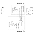
- FIG. 1 is a block diagram showing an example of an operational amplifier according to the first embodiment of the present technology.
- This operational amplifier includes a first amplifier circuit 100 and a second amplifier circuit 200.
- the first amplifier circuit 100 and the second amplifier circuit 200 are differential amplifier circuits, and input signals from the input terminals 11 and 12 of the operational amplifier are similarly input to both of them. Further, the output signal of the second amplifier circuit 200 is output to the output terminals 91 and 92 of the operational amplifier.
- the input signal and output signal of this operational amplifier are differential signals.
- the first amplifier circuit 100 includes a transconductance amplifier 110, an active load 120, and a transconductance amplifier 130.
- the second amplifier circuit 200 includes a transconductance amplifier 210 and an active load 220.
- the transconductance amplifiers 110, 130 and 210 are current-voltage conversion circuits that convert the input voltage into a current.
- the transconductance amplifier 110 generates a current corresponding to the voltage of the input signal from the input terminals 11 and 12.
- the active load 120 is an active load (transistor load) of the transconductance amplifier 110.
- the transconductance amplifier 130 generates a current corresponding to the voltage with respect to the current generated by the transconductance amplifier 110.
- the current generated by the transconductance amplifier 110 becomes a voltage corresponding to the current due to the capacitance 129, and is input to the transconductance amplifier 130 as a voltage.
- the transconductance amplifier 210 generates a current corresponding to the voltage of the input signal from the input terminals 11 and 12.
- the active load 220 is the active load of the transconductance amplifiers 210 and 130.
- the active load 220 is shared by the transconductance amplifiers 210 and 130.
- the active load 220 has a function of adding the current generated by the transconductance amplifier 210 and the current generated by the transconductance amplifier 130.
- the current added in the active load 220 becomes a voltage corresponding to the current due to the capacitance 229, and is output to the output terminals 91 and 92.
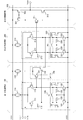
- FIG. 2 is a circuit diagram showing an example of an operational amplifier according to the first embodiment of the present technology.
- this operational amplifier includes a first amplifier circuit 100 and a second amplifier circuit 200.
- the circuits inside the first amplifier circuit 100 and the second amplifier circuit 200 are the transconductance amplifiers 110, 130 and 210 and the active load as described above, except that the current sources 113, 133 and 213 are specified. It includes 120 and 220. Current sources 113, 133 and 213 generate current from the power supply potential VDD.
- the transconductance amplifier 110 includes P-type MOS (Metal-Oxide-Semiconductor) transistors 111 and 112 in which one of the differential input signals is input to the gate.
- the sources of the MOS transistors 111 and 112 are connected to the current source 113.
- the drains of the MOS transistors 111 and 112 are connected to the inputs of the active load 120 and the transconductance amplifier 130.
- the active load 120 includes N-type MOS transistors 121 to 124 and resistors 125 and 126.
- the source of the MOS transistors 121 to 124 is connected to the ground potential VSS.
- MOS transistors 121 and 122 constitute a transconductance amplifier (internal transconductance amplifier of active load 120).
- the output of the transconductance amplifier 110 is connected to the gates of the MOS transistors 121 and 122 via resistors 125 and 126. That is, the resistors 125 and 126 generate a voltage corresponding to the output current of the transconductance amplifier 110, and this voltage is applied between the gate and drain of the MOS transistors 121 and 122.
- the MOS transistors 123 and 124 cross-connect the gate and drain to each other. As a result, the transconductance amplifier composed of the MOS transistors 121 and 122 is positively fed back. That is, the MOS transistors 123 and 124 are positive feedback circuits that positively feed back the output of the transconductance amplifier composed of the MOS transistors 121 and 122 to the input side thereof.
- the transconductance amplifier 130 includes P-type MOS transistors 131 and 132 in which one of the differential signals, which is the output signal of the transconductance amplifier 110, is input to the gate.
- the sources of the MOS transistors 131 and 132 are connected to the current source 133.
- the drains of the MOS transistors 131 and 132 are connected to the input of the active load 220.
- the transconductance amplifier 210 includes P-type MOS transistors 211 and 212 in which one of the differential input signals is input to the gate.
- the sources of the MOS transistors 211 and 212 are connected to the current source 213.
- the drains of the MOS transistors 211 and 212 are connected to the input of the active load 220.
- the active load 220 includes N-type MOS transistors 221 to 224 and resistors 225 and 226.
- the sources of the MOS transistors 221 to 224 are connected to the ground potential VSS.
- MOS transistors 221 and 222 constitute a transconductance amplifier (internal transconductance amplifier of active load 220).
- the output of the transconductance amplifier 210 and the output of the transconductance amplifier 130 are connected to the gates of the MOS transistors 221 and 222 via resistors 225 and 226. That is, the resistors 125 and 126 generate a voltage corresponding to the sum of the output current of the transconductance amplifier 110 and the output current of the transconductance amplifier 130, and this voltage is applied between the gate and drain of the MOS transistors 221 and 222. Will be done.
- the MOS transistors 223 and 224 cross-connect the gate and drain to each other.
- the transconductance amplifier composed of the MOS transistors 221 and 222 is positively fed back. That is, the MOS transistors 223 and 224 are positive feedback circuits that positively feed back the output of the transconductance amplifier composed of the MOS transistors 221 and 222 to the input side thereof.
- the output signal of the transconductance amplifier 210 with the active load 220 as the load is output as the differential output signal of the second amplifier circuit 200.
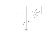
- FIG. 3 is a diagram showing an example of an active load equivalent circuit according to an embodiment of the present technology.
- Each of the active loads 120 and 220 in this embodiment is represented as a load 20 in which the transconductance amplifier 10 is positively fed back.
- a load 20 in which the transconductance amplifier 10 is positively fed back.
- the impedances Z of the active loads 120 and 220 are expressed by the following equations.
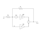
- FIG. 4 is a diagram showing an example of an equivalent circuit of an operational amplifier according to the first embodiment of the present technology.
- the input resistance Rin and the feedback resistance Rf are connected, and the relationship between the off voltage Voff, the input voltage Vin, and the output voltage Vout is examined.
- the mutual conductances of the transconductance amplifiers 110, 130, and 210 are gm1, gm1a, and gm2, respectively. Further, the resistance values of the active loads 120 and 220 are both set to R0.
- the open loop gain (gain) Av1 of the first amplifier circuit 100 is expressed by the following equation.
- Av1 gm1, R0, gm1a, R0
- Av2 gm2 ⁇ R0
- the operational amplifier according to the first embodiment if the gain Av1 of the first amplifier circuit 100 is made sufficiently higher than the gain Av2 of the second amplifier circuit 200, the flicker noise of the second amplifier circuit 200 and the like It is possible to avoid the influence of the offset due to.
- the combination of the first amplifier circuit 100 and the second amplifier circuit 200 does not affect the DC level transfer function.
- a plurality of amplifier circuits can be used by adding the output signals of the first amplifier circuit 100 and the second amplifier circuit 200 by the current. It can. That is, the circuit for controlling the voltage level required in the conventional voltage addition can be omitted.
- a high gain and low speed amplifier circuit is adopted as the first amplifier circuit 100 and a low gain and high speed amplifier circuit is adopted as the second amplifier circuit 200, a high gain and high speed operational amplifier can be obtained as a whole. Be done.
- Second Embodiment> an example in which the operational amplifier of the first embodiment described above is applied to a class AB output amplifier will be described.
- FIG. 5 is a block diagram showing an example of an operational amplifier according to a second embodiment of the present technology.
- the operational amplifier in the second embodiment includes a third amplifier circuit 300 as an output stage in addition to the first amplifier circuit 100 and the second amplifier circuit 200. As a result, signal amplification can be performed according to the application.
- first amplifier circuit 100 and the second amplifier circuit 200 are the same as those in the first embodiment described above, detailed description thereof will be omitted.
- FIG. 6 is a circuit diagram showing an example of an operational amplifier according to a second embodiment of the present technology.
- the class AB output stage is configured as the third amplifier circuit 300. That is, the third amplifier circuit 300 is a class AB amplifier that amplifies the voltage with respect to the output current of the second amplifier circuit 200.
- the third amplifier circuit 300 includes N-type MOS transistors 311 and 312 and P-type MOS transistors 321 and 322, and constitutes a minimum selector push-pull circuit which is a kind of differential amplifier circuit.
- the present technology can have the following configurations.
- a first amplifier circuit that outputs a current according to the input voltage
- An operational amplifier including a second amplifier circuit that outputs a current obtained by adding a current corresponding to the input voltage and a current output from the first amplifier circuit.
- Each of the first and second amplifier circuits has an active load that serves as a load for the transconductance amplifier.
- the active load includes an internal transconductance amplifier that generates a current corresponding to a voltage with respect to the output current of the transconductance amplifier, and a positive feedback circuit that positively feeds back the output of the internal transconductance amplifier to its input side.
- the first amplifier circuit further includes another transconductance amplifier that generates a current corresponding to a voltage with respect to the output current of the transconductance amplifier of the first amplifier circuit.
- the active load of the second amplifier circuit is described in (3) above, which generates a current obtained by adding the output current of the other transconductance amplifier and the output current of the transconductance amplifier of the second amplifier circuit. Operational amplifier.
- Transconductance amplifier 20 Load 100 First amplifier circuit 110 Transconductance amplifier 111, 112 MOS transistor 113 Current source 120 Active load 121 to 124 MOS transistor 125, 126 Resistance 129 Capacity 130 Transconductance amplifier 131, 132 MOS transistor 133 Current source 200 Second amplifier circuit 210 Transconductance amplifier 211, 212 MOS transistor 213 Current source 220 Active load 221 to 224 MOS transistor 225, 226 Resistance 229 Capacity 300 Third amplifier circuit 311, 312, 321, 322 MOS transistor
Landscapes
- Engineering & Computer Science (AREA)
- Power Engineering (AREA)
- Amplifiers (AREA)
Abstract
演算増幅器において電圧レベルの複雑な制御を省く。 演算増幅器は、第1の増幅回路および第2の増幅回路を備える。第1の増幅回路は、入力電圧に応じた電流を出力する。第2の増幅回路は、入力電圧に応じた電流を生成する。第2の増幅回路は、自身が生成した電流と、第1の増幅回路から出力された電流とを加えた電流を出力する。例えば、第1の増幅回路として高ゲインで低速な増幅回路を採用し、第2の増幅回路として低ゲインで高速な増幅回路を採用すれば、電圧レベルの制御のための回路を要することなく、全体として高ゲインで高速な演算増幅器が得られる。
Description
本技術は、演算増幅器に関する。詳しくは、入力電圧を増幅して出力する演算増幅器に関する。
従来、演算増幅器の利得を向上させるために、複数の増幅回路の出力信号を足し合わせる技術が知られている。例えば、2段増幅回路の出力と並列に1段増幅回路を接続して、両者の出力信号を重畳する増幅回路が提案されている(例えば、特許文献1参照。)。
上述の従来技術では、並列に接続される増幅回路の出力信号の位相を同位相にすることにより、直流利得を低下させることなく信号帯域の広域化を図っている。しかしながら、従来技術では増幅回路の出力信号を電圧レベルで加算しているため、直流成分を除去するための容量が必要になる。また、差動信号を扱う場合には、コモンモード電圧を決定するためにコモンフィードバック回路が必要になる。
本技術はこのような状況に鑑みて生み出されたものであり、演算増幅器において電圧レベルの制御に必要な回路を省くことを目的とする。
本技術は、上述の問題点を解消するためになされたものであり、その第1の側面は、入力電圧に応じた電流を出力する第1の増幅回路と、上記入力電圧に応じた電流と上記第1の増幅回路から出力された電流とを加えた電流を出力する第2の増幅回路とを具備する演算増幅器である。これにより、2つの増幅回路の出力を電流加算して出力するという作用をもたらす。
また、この第1の側面において、上記第1および第2の増幅回路の各々は、上記入力電圧に応じた電流を生成するトランスコンダクタンスアンプを備えるようにしてもよい。この場合において、上記第1および第2の増幅回路の各々は、上記トランスコンダクタンスアンプの負荷となるアクティブロードを備え、上記アクティブロードは、上記トランスコンダクタンスアンプの出力電流に対する電圧に応じた電流を生成する内部トランスコンダクタンスアンプと、上記内部トランスコンダクタンスアンプの出力をその入力側に正帰還させる正帰還回路とを備えてもよい。正帰還をかけたアクティブロードを利用することにより、増幅回路として高ゲイン化を図るという作用をもたらす。
また、この第1の側面において、上記第1の増幅回路は、上記第1の増幅回路の上記トランスコンダクタンスアンプの出力電流に対する電圧に応じた電流を生成する他のトランスコンダクタンスアンプをさらに備え、上記第2の増幅回路の上記アクティブロードは、上記他のトランスコンダクタンスアンプの出力電流と上記第2の増幅回路の上記トランスコンダクタンスアンプの出力電流とを加算した電流を生成するようにしてもよい。これにより、第2の増幅回路のアクティブロードにおいて電流加算を行うという作用をもたらす。
また、この第1の側面において、上記第1の増幅回路のゲインは上記第2の増幅回路のゲインよりも高く、また、上記第1の増幅回路の速度は上記第2の増幅回路の速度よりも遅い場合を想定すると、全体として高ゲインで高速な演算増幅器が得られる。
また、この第1の側面において、上記第1および第2の増幅回路の各々は、差動増幅回路であってもよい。この場合であっても、電流加算を前提とすることにより、コモンフィードバック回路は不要となる。
また、この第1の側面において、上記第2の増幅回路の出力電流に対する電圧を増幅して出力する第3の増幅回路をさらに具備してもよい。この場合において、上記第3の増幅回路は、プッシュプル回路であってもよく、また、AB級アンプであってもよい。すなわち、用途に応じたアンプを出力段として利用可能である。
以下、本技術を実施するための形態(以下、実施の形態と称する)について説明する。説明は以下の順序により行う。
1.第1の実施の形態(2つの増幅回路の出力を電流加算した例)
2.第2の実施の形態(AB級出力アンプに適用した例)
1.第1の実施の形態(2つの増幅回路の出力を電流加算した例)
2.第2の実施の形態(AB級出力アンプに適用した例)
<1.第1の実施の形態>
[演算増幅器]
図1は、本技術の第1の実施の形態における演算増幅器の一例を示すブロック図である。
[演算増幅器]
図1は、本技術の第1の実施の形態における演算増幅器の一例を示すブロック図である。
この演算増幅器は、第1の増幅回路100と、第2の増幅回路200とを備える。第1の増幅回路100および第2の増幅回路200は差動増幅回路であり、何れにも演算増幅器の入力端子11および12からの入力信号が同様に入力される。また、第2の増幅回路200の出力信号が演算増幅器の出力端子91および92に出力される。この演算増幅器の入力信号および出力信号は、差動信号である。
第1の増幅回路100は、トランスコンダクタンスアンプ110と、アクティブロード120と、トランスコンダクタンスアンプ130とを備える。また、第2の増幅回路200は、トランスコンダクタンスアンプ210と、アクティブロード220とを備える。
トランスコンダクタンスアンプ110、130および210は、入力された電圧を電流に変換する電流電圧変換回路である。
トランスコンダクタンスアンプ110は、入力端子11および12からの入力信号の電圧に応じた電流を生成する。アクティブロード120は、トランスコンダクタンスアンプ110の能動負荷(トランジスタ負荷)である。
トランスコンダクタンスアンプ130は、トランスコンダクタンスアンプ110によって生成された電流に対する電圧に応じた電流を生成する。なお、トランスコンダクタンスアンプ110によって生成された電流は、容量129によってその電流に応じた電圧となり、電圧としてトランスコンダクタンスアンプ130に入力される。
トランスコンダクタンスアンプ210は、入力端子11および12からの入力信号の電圧に応じた電流を生成する。アクティブロード220は、トランスコンダクタンスアンプ210および130の能動負荷である。
このように、このアクティブロード220は、トランスコンダクタンスアンプ210および130に共有される。これにより、このアクティブロード220は、トランスコンダクタンスアンプ210によって生成された電流と、トランスコンダクタンスアンプ130によって生成された電流とを加算する機能を有する。このアクティブロード220において加算された電流は、容量229によってその電流に応じた電圧となり、出力端子91および92に出力される。
[回路]
図2は、本技術の第1の実施の形態における演算増幅器の一例を示す回路図である。
図2は、本技術の第1の実施の形態における演算増幅器の一例を示す回路図である。
上述のブロック図について説明したように、この演算増幅器は、第1の増幅回路100と、第2の増幅回路200とを備える。第1の増幅回路100および第2の増幅回路200の内部の回路は、電流源113、133および213を明示した点を除き、上述のように、トランスコンダクタンスアンプ110、130および210と、アクティブロード120および220を備える。電流源113、133および213は、電源電位VDDから電流を生成するものである。
トランスコンダクタンスアンプ110は、差動入力信号の一方がゲートに入力されるP型のMOS(Metal-Oxide-Semiconductor)トランジスタ111および112を備える。MOSトランジスタ111および112のソースは、電流源113に接続される。MOSトランジスタ111および112のドレインは、アクティブロード120およびトランスコンダクタンスアンプ130の入力に接続される。
アクティブロード120は、N型のMOSトランジスタ121乃至124と、抵抗125および126とを備える。MOSトランジスタ121乃至124のソースは、接地電位VSSに接続される。
MOSトランジスタ121および122は、トランスコンダクタンスアンプ(アクティブロード120の内部トランスコンダクタンスアンプ)を構成する。MOSトランジスタ121および122のゲートには、抵抗125および126を介してトランスコンダクタンスアンプ110の出力が接続される。すなわち、抵抗125および126はトランスコンダクタンスアンプ110の出力電流に応じた電圧を生成し、この電圧がMOSトランジスタ121および122のゲート・ドレイン間に印加される。
また、MOSトランジスタ123および124は、ゲート・ドレインを互いにクロス接続する。これにより、MOSトランジスタ121および122により構成されるトランスコンダクタンスアンプに正帰還をかけた構造となる。すなわち、MOSトランジスタ123および124は、MOSトランジスタ121および122により構成されるトランスコンダクタンスアンプの出力をその入力側に正帰還させる正帰還回路である。
トランスコンダクタンスアンプ130は、トランスコンダクタンスアンプ110の出力信号である差動信号の一方がゲートに入力されるP型のMOSトランジスタ131および132を備える。MOSトランジスタ131および132のソースは、電流源133に接続される。MOSトランジスタ131および132のドレインは、アクティブロード220の入力に接続される。
トランスコンダクタンスアンプ210は、差動入力信号の一方がゲートに入力されるP型のMOSトランジスタ211および212を備える。MOSトランジスタ211および212のソースは、電流源213に接続される。MOSトランジスタ211および212のドレインは、アクティブロード220の入力に接続される。
アクティブロード220は、N型のMOSトランジスタ221乃至224と、抵抗225および226とを備える。MOSトランジスタ221乃至224のソースは、接地電位VSSに接続される。
MOSトランジスタ221および222は、トランスコンダクタンスアンプ(アクティブロード220の内部トランスコンダクタンスアンプ)を構成する。MOSトランジスタ221および222のゲートには、抵抗225および226を介してトランスコンダクタンスアンプ210の出力およびトランスコンダクタンスアンプ130の出力が接続される。すなわち、抵抗125および126はトランスコンダクタンスアンプ110の出力電流とトランスコンダクタンスアンプ130の出力電流とを加算した電流に応じた電圧を生成し、この電圧がMOSトランジスタ221および222のゲート・ドレイン間に印加される。
また、MOSトランジスタ223および224は、ゲート・ドレインを互いにクロス接続する。これにより、MOSトランジスタ221および222により構成されるトランスコンダクタンスアンプに正帰還をかけた構造となる。すなわち、MOSトランジスタ223および224は、MOSトランジスタ221および222により構成されるトランスコンダクタンスアンプの出力をその入力側に正帰還させる正帰還回路である。
アクティブロード220を負荷とするトランスコンダクタンスアンプ210の出力信号は、第2の増幅回路200の差動出力信号として出力される。
[アクティブロード]
図3は、本技術の実施の形態におけるアクティブロードの等価回路の例を示す図である。
図3は、本技術の実施の形態におけるアクティブロードの等価回路の例を示す図である。
この実施の形態におけるアクティブロード120および220の各々は、トランスコンダクタンスアンプ10に正帰還をかけた負荷20として表される。正帰還をかけたアクティブロードを利用することにより、増幅回路として高ゲイン化を図ることができる。また、正帰還をかけたアクティブロードは、自動的にコモン電圧(平均電圧)が決定されるため、コモンフィードバック回路は不要になる。
ここで、トランスコンダクタンスアンプ10の相互コンダクタンスをgm0、負荷20の抵抗値をR0とすると、アクティブロード120および220のインピーダンスZは次式により表される。
Z=-(R0/gm0)/(R0-(1/gm0))
=R0/(gm0・R0-1)
したがって、このインピーダンスZは、gm0が「1/R0」である場合を境として、その極性が反転することがわかる。
Z=-(R0/gm0)/(R0-(1/gm0))
=R0/(gm0・R0-1)
したがって、このインピーダンスZは、gm0が「1/R0」である場合を境として、その極性が反転することがわかる。
[伝達特性]
図4は、本技術の第1の実施の形態における演算増幅器の等価回路の例を示す図である。
図4は、本技術の第1の実施の形態における演算増幅器の等価回路の例を示す図である。
ここでは、演算増幅器の伝達特性を解析するために、入力抵抗Rin、帰還抵抗Rfを接続して、オフ電圧Voff、入力電圧Vinおよび出力電圧Voutの関係について検討する。
トランスコンダクタンスアンプ110、130、210の相互コンダクタンスを、それぞれgm1、gm1a、gm2とする。また、アクティブロード120および220の抵抗値を、ともにR0とする。
このとき、第1の増幅回路100のオープンループ利得(ゲイン)Av1は、次式により表される。
Av1=gm1・R0・gm1a・R0
Av1=gm1・R0・gm1a・R0
また、第2の増幅回路200のオープンループ利得(ゲイン)Av2は、次式により表される。
Av2=gm2・R0
Av2=gm2・R0
まず、オフ電圧Voffと出力電圧Voutの関係を次式に示す。

上式において、Av1>>Av2を満たす場合には、

となる。すなわち、この場合は、第2の増幅回路200のオフセットは出力電圧に表れなくなる。
一方、Av1<<Av2となる場合には、
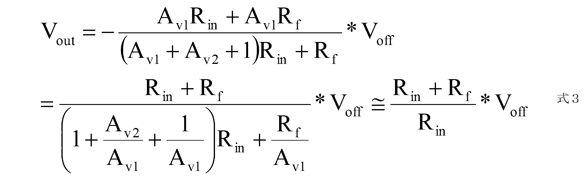
となる。すなわち、この場合は、第2の増幅回路200のオフセットが出力電圧に表れることになる。
したがって、この第1の実施の形態における演算増幅器においては、第1の増幅回路100のゲインAv1を第2の増幅回路200のゲインAv2よりも十分高くすると、第2の増幅回路200のフリッカーノイズ等によるオフセットの影響を回避することができる。
次に、入力電圧Vinと出力電圧Voutの関係を次式に示す。
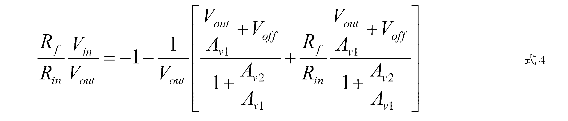
上式を変形すると、次式が得られる。

したがって、第1の増幅回路100および第2の増幅回路200を組み合わせても、直流レベルの伝達関数には影響を与えないことが分かる。
このように、本技術の第1の実施の形態によれば、第1の増幅回路100および第2の増幅回路200の出力信号を電流により加算することにより、複数の増幅回路を利用することができる。すなわち、従来の電圧加算において必要とされた電圧レベルの制御のための回路を省くことができる。特に、第1の増幅回路100として高ゲインで低速な増幅回路を採用し、第2の増幅回路200として低ゲインで高速な増幅回路を採用すれば、全体として高ゲインで高速な演算増幅器が得られる。
<2.第2の実施の形態>
この第2の実施の形態では、上述の第1の実施の形態の演算増幅器をAB級出力アンプに適用した例について説明する。
この第2の実施の形態では、上述の第1の実施の形態の演算増幅器をAB級出力アンプに適用した例について説明する。
[演算増幅器]
図5は、本技術の第2の実施の形態における演算増幅器の一例を示すブロック図である。
図5は、本技術の第2の実施の形態における演算増幅器の一例を示すブロック図である。
この第2の実施の形態における演算増幅器は、第1の増幅回路100および第2の増幅回路200に加えて、出力段として第3の増幅回路300を備える。これにより、用途に応じた信号増幅を行うことができる。
なお、第1の増幅回路100および第2の増幅回路200については、上述の第1の実施の形態と同様であるため、詳細な説明は省略する。
[回路]
図6は、本技術の第2の実施の形態における演算増幅器の一例を示す回路図である。
図6は、本技術の第2の実施の形態における演算増幅器の一例を示す回路図である。
この例では、オーディオアンプを想定して、第3の増幅回路300として、AB級出力段を構成している。すなわち、この第3の増幅回路300は、第2の増幅回路200の出力電流に対する電圧を増幅するAB級アンプである。
この第3の増幅回路300は、N型のMOSトランジスタ311および312と、P型のMOSトランジスタ321および322を備え、差動増幅回路の一種であるミニマムセレクタ・プッシュプル回路を構成する。
このように、本技術の第2の実施の形態によれば、用途に応じた出力段を備える演算増幅器を構成することができる。
なお、上述の実施の形態は本技術を具現化するための一例を示したものであり、実施の形態における事項と、特許請求の範囲における発明特定事項とはそれぞれ対応関係を有する。同様に、特許請求の範囲における発明特定事項と、これと同一名称を付した本技術の実施の形態における事項とはそれぞれ対応関係を有する。ただし、本技術は実施の形態に限定されるものではなく、その要旨を逸脱しない範囲において実施の形態に種々の変形を施すことにより具現化することができる。
なお、本明細書に記載された効果はあくまで例示であって、限定されるものではなく、また、他の効果があってもよい。
なお、本技術は以下のような構成もとることができる。
(1)入力電圧に応じた電流を出力する第1の増幅回路と、
前記入力電圧に応じた電流と前記第1の増幅回路から出力された電流とを加えた電流を出力する第2の増幅回路と
を具備する演算増幅器。
(2)前記第1および第2の増幅回路の各々は、前記入力電圧に応じた電流を生成するトランスコンダクタンスアンプを備える
前記(1)に記載の演算増幅器。
(3)前記第1および第2の増幅回路の各々は、前記トランスコンダクタンスアンプの負荷となるアクティブロードを備え、
前記アクティブロードは、前記トランスコンダクタンスアンプの出力電流に対する電圧に応じた電流を生成する内部トランスコンダクタンスアンプと、前記内部トランスコンダクタンスアンプの出力をその入力側に正帰還させる正帰還回路とを備える
前記(2)に記載の演算増幅器。
(4)前記第1の増幅回路は、前記第1の増幅回路の前記トランスコンダクタンスアンプの出力電流に対する電圧に応じた電流を生成する他のトランスコンダクタンスアンプをさらに備え、
前記第2の増幅回路の前記アクティブロードは、前記他のトランスコンダクタンスアンプの出力電流と前記第2の増幅回路の前記トランスコンダクタンスアンプの出力電流とを加算した電流を生成する
前記(3)に記載の演算増幅器。
(5)前記第1の増幅回路のゲインは前記第2の増幅回路のゲインよりも高い
前記(1)から(4)のいずれかに記載の演算増幅器。
(6)前記第1の増幅回路の速度は前記第2の増幅回路の速度よりも遅い
前記(1)から(5)のいずれかに記載の演算増幅器。
(7)前記第1および第2の増幅回路の各々は、差動増幅回路である
前記(1)から(6)のいずれかに記載の演算増幅器。
(8)前記第2の増幅回路の出力電流に対する電圧を増幅して出力する第3の増幅回路をさらに具備する前記(1)から(7)のいずれかに記載の演算増幅器。
(9)前記第3の増幅回路は、プッシュプル回路である
前記(8)に記載の演算増幅器。
(10)前記第3の増幅回路は、AB級アンプである
前記(8)または(9)に記載の演算増幅器。
(1)入力電圧に応じた電流を出力する第1の増幅回路と、
前記入力電圧に応じた電流と前記第1の増幅回路から出力された電流とを加えた電流を出力する第2の増幅回路と
を具備する演算増幅器。
(2)前記第1および第2の増幅回路の各々は、前記入力電圧に応じた電流を生成するトランスコンダクタンスアンプを備える
前記(1)に記載の演算増幅器。
(3)前記第1および第2の増幅回路の各々は、前記トランスコンダクタンスアンプの負荷となるアクティブロードを備え、
前記アクティブロードは、前記トランスコンダクタンスアンプの出力電流に対する電圧に応じた電流を生成する内部トランスコンダクタンスアンプと、前記内部トランスコンダクタンスアンプの出力をその入力側に正帰還させる正帰還回路とを備える
前記(2)に記載の演算増幅器。
(4)前記第1の増幅回路は、前記第1の増幅回路の前記トランスコンダクタンスアンプの出力電流に対する電圧に応じた電流を生成する他のトランスコンダクタンスアンプをさらに備え、
前記第2の増幅回路の前記アクティブロードは、前記他のトランスコンダクタンスアンプの出力電流と前記第2の増幅回路の前記トランスコンダクタンスアンプの出力電流とを加算した電流を生成する
前記(3)に記載の演算増幅器。
(5)前記第1の増幅回路のゲインは前記第2の増幅回路のゲインよりも高い
前記(1)から(4)のいずれかに記載の演算増幅器。
(6)前記第1の増幅回路の速度は前記第2の増幅回路の速度よりも遅い
前記(1)から(5)のいずれかに記載の演算増幅器。
(7)前記第1および第2の増幅回路の各々は、差動増幅回路である
前記(1)から(6)のいずれかに記載の演算増幅器。
(8)前記第2の増幅回路の出力電流に対する電圧を増幅して出力する第3の増幅回路をさらに具備する前記(1)から(7)のいずれかに記載の演算増幅器。
(9)前記第3の増幅回路は、プッシュプル回路である
前記(8)に記載の演算増幅器。
(10)前記第3の増幅回路は、AB級アンプである
前記(8)または(9)に記載の演算増幅器。
10 トランスコンダクタンスアンプ
20 負荷
100 第1の増幅回路
110 トランスコンダクタンスアンプ
111、112 MOSトランジスタ
113 電流源
120 アクティブロード
121~124 MOSトランジスタ
125、126 抵抗
129 容量
130 トランスコンダクタンスアンプ
131、132 MOSトランジスタ
133 電流源
200 第2の増幅回路
210 トランスコンダクタンスアンプ
211、212 MOSトランジスタ
213 電流源
220 アクティブロード
221~224 MOSトランジスタ
225、226 抵抗
229 容量
300 第3の増幅回路
311、312、321、322 MOSトランジスタ
20 負荷
100 第1の増幅回路
110 トランスコンダクタンスアンプ
111、112 MOSトランジスタ
113 電流源
120 アクティブロード
121~124 MOSトランジスタ
125、126 抵抗
129 容量
130 トランスコンダクタンスアンプ
131、132 MOSトランジスタ
133 電流源
200 第2の増幅回路
210 トランスコンダクタンスアンプ
211、212 MOSトランジスタ
213 電流源
220 アクティブロード
221~224 MOSトランジスタ
225、226 抵抗
229 容量
300 第3の増幅回路
311、312、321、322 MOSトランジスタ
Claims (10)
- 入力電圧に応じた電流を出力する第1の増幅回路と、
前記入力電圧に応じた電流と前記第1の増幅回路から出力された電流とを加えた電流を出力する第2の増幅回路と
を具備する演算増幅器。 - 前記第1および第2の増幅回路の各々は、前記入力電圧に応じた電流を生成するトランスコンダクタンスアンプを備える
請求項1記載の演算増幅器。 - 前記第1および第2の増幅回路の各々は、前記トランスコンダクタンスアンプの負荷となるアクティブロードを備え、
前記アクティブロードは、前記トランスコンダクタンスアンプの出力電流に対する電圧に応じた電流を生成する内部トランスコンダクタンスアンプと、前記内部トランスコンダクタンスアンプの出力をその入力側に正帰還させる正帰還回路とを備える
請求項2記載の演算増幅器。 - 前記第1の増幅回路は、前記第1の増幅回路の前記トランスコンダクタンスアンプの出力電流に対する電圧に応じた電流を生成する他のトランスコンダクタンスアンプをさらに備え、
前記第2の増幅回路の前記アクティブロードは、前記他のトランスコンダクタンスアンプの出力電流と前記第2の増幅回路の前記トランスコンダクタンスアンプの出力電流とを加算した電流を生成する
請求項3記載の演算増幅器。 - 前記第1の増幅回路のゲインは前記第2の増幅回路のゲインよりも高い
請求項1記載の演算増幅器。 - 前記第1の増幅回路の速度は前記第2の増幅回路の速度よりも遅い
請求項1記載の演算増幅器。 - 前記第1および第2の増幅回路の各々は、差動増幅回路である
請求項1記載の演算増幅器。 - 前記第2の増幅回路の出力電流に対する電圧を増幅して出力する第3の増幅回路をさらに具備する請求項1記載の演算増幅器。
- 前記第3の増幅回路は、プッシュプル回路である
請求項8記載の演算増幅器。 - 前記第3の増幅回路は、AB級アンプである
請求項8記載の演算増幅器。
Priority Applications (1)
| Application Number | Priority Date | Filing Date | Title |
|---|---|---|---|
| JP2021554074A JP7550162B2 (ja) | 2019-10-29 | 2020-07-14 | 演算増幅器 |
Applications Claiming Priority (2)
| Application Number | Priority Date | Filing Date | Title |
|---|---|---|---|
| JP2019195804 | 2019-10-29 | ||
| JP2019-195804 | 2019-10-29 |
Publications (1)
| Publication Number | Publication Date |
|---|---|
| WO2021084809A1 true WO2021084809A1 (ja) | 2021-05-06 |
Family
ID=75714619
Family Applications (1)
| Application Number | Title | Priority Date | Filing Date |
|---|---|---|---|
| PCT/JP2020/027316 Ceased WO2021084809A1 (ja) | 2019-10-29 | 2020-07-14 | 演算増幅器 |
Country Status (2)
| Country | Link |
|---|---|
| JP (1) | JP7550162B2 (ja) |
| WO (1) | WO2021084809A1 (ja) |
Citations (2)
| Publication number | Priority date | Publication date | Assignee | Title |
|---|---|---|---|---|
| US20030122624A1 (en) * | 2001-12-21 | 2003-07-03 | Stmicroelectronics S.R.L | Analog input circuit with common mode compatibility to both supply nodes |
| JP2017079397A (ja) * | 2015-10-20 | 2017-04-27 | 株式会社東芝 | 増幅回路 |
Family Cites Families (1)
| Publication number | Priority date | Publication date | Assignee | Title |
|---|---|---|---|---|
| GB0407663D0 (en) | 2004-04-03 | 2004-05-05 | Ibm | Variable gain amplifier |
-
2020
- 2020-07-14 WO PCT/JP2020/027316 patent/WO2021084809A1/ja not_active Ceased
- 2020-07-14 JP JP2021554074A patent/JP7550162B2/ja active Active
Patent Citations (2)
| Publication number | Priority date | Publication date | Assignee | Title |
|---|---|---|---|---|
| US20030122624A1 (en) * | 2001-12-21 | 2003-07-03 | Stmicroelectronics S.R.L | Analog input circuit with common mode compatibility to both supply nodes |
| JP2017079397A (ja) * | 2015-10-20 | 2017-04-27 | 株式会社東芝 | 増幅回路 |
Also Published As
| Publication number | Publication date |
|---|---|
| JPWO2021084809A1 (ja) | 2021-05-06 |
| JP7550162B2 (ja) | 2024-09-12 |
Similar Documents
| Publication | Publication Date | Title |
|---|---|---|
| US6114907A (en) | Amplifier with dynamic compensation and method | |
| US7973605B2 (en) | Three-stage frequency-compensated operational amplifier for driving large capacitive loads | |
| US5210506A (en) | Large swing output buffer amplifier | |
| US6285259B1 (en) | System and method for converting from single-ended to differential signals | |
| EP0138261A2 (en) | Differential operational amplifier with common mode feedback | |
| US6577184B2 (en) | Switched-capacitor, common-mode feedback circuit for a differential amplifier without tail current | |
| US8519786B2 (en) | Variable gain amplifier with fixed bandwidth | |
| US20100109779A1 (en) | Hybrid class ab super follower | |
| JP2004343277A (ja) | 入力バッファ回路 | |
| JP3040974B2 (ja) | Cmosレール−レール間入出力増幅器 | |
| US20190363679A1 (en) | Negative capacitance circuits including temperature-compensation biasings | |
| US11664774B2 (en) | Operational amplifier using single-stage amplifier with slew-rate enhancement and associated method | |
| US6833760B1 (en) | Low power differential amplifier powered by multiple unequal power supply voltages | |
| US6525608B2 (en) | High gain, high bandwidth, fully differential amplifier | |
| US7292098B2 (en) | Operational amplifier | |
| US20040164807A1 (en) | Limiting amplifier with active inductor | |
| CN101521489A (zh) | 放大器和ab类放大器 | |
| US20050035819A1 (en) | CMOS differential buffer circuit | |
| EP0228215B1 (en) | Field-effect transistor amplifier circuits | |
| US5406220A (en) | Pole/zero compensation in cascode amplifiers | |
| US8803609B2 (en) | Bandwidth extension of an amplifier | |
| US20170322574A1 (en) | Voltage-to-current converter | |
| JP7550162B2 (ja) | 演算増幅器 | |
| US6710660B1 (en) | Class B power buffer with rail to rail output swing and small deadband | |
| EP1124326A1 (en) | An operational amplifier with high gain and sysmmetrical output-current capabilty |
Legal Events
| Date | Code | Title | Description |
|---|---|---|---|
| 121 | Ep: the epo has been informed by wipo that ep was designated in this application |
Ref document number: 20882246 Country of ref document: EP Kind code of ref document: A1 |
|
| ENP | Entry into the national phase |
Ref document number: 2021554074 Country of ref document: JP Kind code of ref document: A |
|
| NENP | Non-entry into the national phase |
Ref country code: DE |
|
| 122 | Ep: pct application non-entry in european phase |
Ref document number: 20882246 Country of ref document: EP Kind code of ref document: A1 |