WO2021079573A1 - 撮像装置および記憶装置 - Google Patents
撮像装置および記憶装置 Download PDFInfo
- Publication number
- WO2021079573A1 WO2021079573A1 PCT/JP2020/027598 JP2020027598W WO2021079573A1 WO 2021079573 A1 WO2021079573 A1 WO 2021079573A1 JP 2020027598 W JP2020027598 W JP 2020027598W WO 2021079573 A1 WO2021079573 A1 WO 2021079573A1
- Authority
- WO
- WIPO (PCT)
- Prior art keywords
- power supply
- memory modules
- memory
- imaging device
- control unit
- Prior art date
- Legal status (The legal status is an assumption and is not a legal conclusion. Google has not performed a legal analysis and makes no representation as to the accuracy of the status listed.)
- Ceased
Links
Images





Classifications
-
- H—ELECTRICITY
- H04—ELECTRIC COMMUNICATION TECHNIQUE
- H04N—PICTORIAL COMMUNICATION, e.g. TELEVISION
- H04N25/00—Circuitry of solid-state image sensors [SSIS]; Control thereof
- H04N25/70—SSIS architectures; Circuits associated therewith
- H04N25/76—Addressed sensors, e.g. MOS or CMOS sensors
- H04N25/78—Readout circuits for addressed sensors, e.g. output amplifiers or A/D converters
-
- H—ELECTRICITY
- H04—ELECTRIC COMMUNICATION TECHNIQUE
- H04N—PICTORIAL COMMUNICATION, e.g. TELEVISION
- H04N25/00—Circuitry of solid-state image sensors [SSIS]; Control thereof
- H04N25/70—SSIS architectures; Circuits associated therewith
-
- H—ELECTRICITY
- H10—SEMICONDUCTOR DEVICES; ELECTRIC SOLID-STATE DEVICES NOT OTHERWISE PROVIDED FOR
- H10B—ELECTRONIC MEMORY DEVICES
- H10B10/00—Static random access memory [SRAM] devices
Definitions
- This technology is related to storage devices. More specifically, the present invention relates to a storage device and an imaging device including a plurality of memory modules.
- an image pickup device In the image pickup device, there is a problem that noise is generated by the switching operation when supplying the drive power to the image pickup device, and the noise is superimposed on the image pickup signal. Therefore, for example, an image pickup device has been proposed in which a power supply switching operation is not performed during a period in which the image pickup element generates or processes a photoelectric conversion signal (see, for example, Patent Document 1).
- the switching operation is controlled so as not to be performed during the period when the electric charge is transferred from the photoelectric conversion element to the floating diffusion element.
- the pixel signal may be temporarily held in the image memory.
- This image memory is often composed of a plurality of memory modules, and the power supply is liable to fluctuate. Therefore, when the power supply to the image memory fluctuates, the fluctuation may become a noise source in the image sensor.
- This technology was created in view of this situation, and aims to suppress fluctuations in power supply in a storage device equipped with a plurality of memory modules.
- the present technology has been made to solve the above-mentioned problems, and the first aspect thereof is a pixel array portion in which a plurality of pixels for photoelectric conversion of light from a subject are arranged, and the plurality of pixels.
- An analog-digital converter that converts an analog signal into a pixel signal based on a digital signal, a plurality of memory modules that hold the pixel signal converted by the analog-digital converter, and a power supply current shared by the plurality of memory modules.
- a control unit that independently controls the operation of each of the plurality of memory modules so that the total of the power supply lines supplied to the power supply lines and the power supply currents supplied to the plurality of memory modules sharing the power supply line is constant.
- the plurality of memory modules are SRAMs
- the control unit may control the retention of the SRAMs. That is, the control unit controls the operation of each of the memory modules by controlling the retention of the SRAM. In this case, the control unit may control the retention of the SRAM so that a predetermined number of memory modules among the plurality of memory modules are active. This has the effect of making the sum of the supplied power supply currents constant for the SRAM that shares the power supply line.
- the power supply line is a plurality of power supply lines for supplying power supply currents from a plurality of different power supply pads, and the plurality of memory modules share each of the plurality of power supply lines. It may be divided into power supply groups. This has the effect of making the sum of the power supply currents supplied to the memory modules in the power supply group constant.
- control unit may control the plurality of memory modules having the same module number in the power supply group to perform the same operation. This has the effect of aligning the control of the memory modules between the power supply groups.
- those having the same module number in the power supply group among the plurality of memory modules are arranged at positions where the distances from the power supply pads are equal to each other. May be good. This has the effect of unifying the behavior of the power supply current of the memory module for each power supply group.
- those having the same module number in the power supply group among the plurality of memory modules are arranged at positions where the distances from the power supply pads are different from each other. May be good. This has the effect of making the voltage drop in the power supply line different for each power supply group.
- those having the same module number in the power supply group among the plurality of memory modules are arranged at random positions from the power supply pad. May be good. This has the effect of distributing the voltage drop pattern in the power supply line for each power supply group.
- FIG. 1 is a diagram showing an example of the overall configuration of the image sensor 100 according to the embodiment of the present technology.
- the image sensor 100 includes a pixel array unit 110, a pixel drive unit 111, a column processing unit 121, an image memory 130, a system control unit 151, and a signal processing unit 154.
- the image sensor 100 is an example of the image pickup apparatus described in the claims.
- the pixel array unit 110 is formed by arranging a plurality of pixels for photoelectric conversion of light from a subject in an array.
- the pixel drive unit 111 drives the pixels of the pixel array unit 110 row by row (horizontal line).
- the column processing unit 121 processes the pixel values of each column (vertical column) read from the pixel array unit 110. More specifically, the column processing unit 121 AD (Analog-to-Digital) converts the analog signal of the pixel of each column into the pixel signal of the digital signal. The pixel signal generated in this way is supplied to the image memory 130 and temporarily held.
- the column processing unit 121 is an example of the analog-to-digital conversion unit described in the claims.
- the image memory 130 is a memory that temporarily holds the pixel signal supplied from the column processing unit 121 as image data. As will be described later, the image memory 130 includes a plurality of memory modules.
- the image memory 130 includes, for example, an SRAM (Static Random Access Memory) as a storage element. Compared to DRAM (Dynamic Random Access Memory), this SRAM does not require a refresh operation, has high access speed, and consumes less power.
- SRAM Static Random Access Memory
- SRAM can perform control called "retention" that cannot be rewritten while retaining data.
- retention is off, SRAM is active and can be rewritten.
- retention is turned on, the SRAM goes to sleep. As a result, the leakage current of the SRAM can be reduced.
- the signal processing unit 154 performs predetermined signal processing on the image data held in the image memory 130.
- the signal processing for example, demosaic processing, white balance processing, and the like are assumed.
- the system control unit 151 controls each unit of the image sensor 100.
- the system control unit 151 independently controls the operation of each of the plurality of memory modules of the image memory 130.
- the system control unit 151 is an example of the control unit described in the claims.
- the memory power supply is supplied to the image sensor 100 via the signal line 132, and the logic power supply is supplied via the signal line 158. Further, a memory control signal is supplied from the system control unit 151 to the image memory 130 via the signal line 131.
- FIG. 2 is a diagram showing an example of a mounting image of the image sensor 100 in the embodiment of the present technology.
- the image sensor 100 assumes a laminated structure. As shown in a in the figure, the pixel array unit 110 occupies most of the area of the first layer. On the other hand, as shown in b in the figure, other circuits are housed in the second layer. The first layer and the second layer are connected between the via regions 191 and 192.
- the AD converter 120 includes the above-mentioned column processing unit 121, and AD-converts a pixel analog signal into a pixel signal based on a digital signal.
- the output circuit 150 includes the above-mentioned system control unit 151 and signal processing unit 154, and outputs from the image sensor 100 to the outside.
- the peripheral circuit 140 is a peripheral circuit including an analog bias circuit of each part of the image sensor 100.
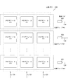
- FIG. 3 is a diagram showing a configuration example of the image memory 130 according to the embodiment of the present technology.
- the image memory 130 includes a plurality of memory modules. These plurality of memory modules are divided into power supply groups that share the power supply pad 139. In this example, it is divided into M + 1 power supply groups # 0 to # M (M is an integer of 0 or more). However, although a plurality of power supply groups are shown in this example, one power supply group may be used as the minimum configuration.
- a module number is assigned to each memory module in the power supply group.
- module numbers # 0 to # 2 are assigned to each of the three memory modules.
- those having the same module number in the power supply group are controlled to perform the same operation. That is, when the system control unit 151 controls the retention of the memory module # 0 to be turned off via the signal line 131, the memory modules # 0 in all the power supply groups become active. That is, such control by the system control unit 151 is performed independently for the memory modules in the power supply group.
- Power for memory is supplied to each of the power pads 139 via the signal line 132. Further, the memory control signal is supplied to the memory modules having the same module number in the power supply group via the signal line 131.
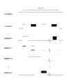
- FIG. 4 is a diagram showing an operation example of the image memory 130 according to the embodiment of the present technology.
- SRAM has retention control, which allows transitions between active and sleep states. For example, if the control signal # 0 is at the H level, the memory module # 0 is activated, and if the control signal # 0 is at the L level, the memory module # 0 goes to sleep.
- two of the three memory modules are controlled to be active during the memory usage period.
- the total power supply current (total memory current) consumed by the memory modules in the power supply group is also constant. Therefore, fluctuations in the current of the power supply supplied to the memory module are suppressed.
- the current fluctuation of each part also affects the pixel array unit 110, and unnecessary horizontal stripes are formed. May adversely affect the quality of the generated image.
- the number of memory modules in the power supply group is set to 3 in order to explain the principle of the present technology, but in the following, the memory modules in the power supply group are also considered in order to consider the arrangement of the memory modules.
- the number of is described as N + 1 (N is an integer of 1 or more).
- N is an integer of 1 or more.
- the memory modules having the same module number in the power supply group are controlled so as to perform the same operation.
- a diagram in which the entire arrangement is rotated by 90 degrees is used.
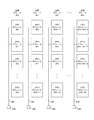
- FIG. 5 is a diagram showing a first arrangement example of the image memory 130 according to the embodiment of the present technology.
- the memory modules in the power supply group share the power supply line 138 connected to one power supply pad 139. Then, in each of the power supply groups, those having a common module number are connected to the power supply line 138 in the same order. Therefore, those having the same module number have the same distance from the power pad 139. As a result, the behavior of the power supply current of the memory module for each power supply group can be unified.
- FIG. 6 is a diagram showing an operation example in the first arrangement example of the image memory 130 according to the embodiment of the present technology.
- the memory module # N and the memory module # 1 are activated at the same time, and then the memory module # 1 and the memory module # 2 are activated at the same time. In this way, when the memory module # N-1 and the memory module # N are activated at the same time, the writing for one frame is completed.
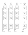
- FIG. 7 is a diagram showing a second arrangement example of the image memory 130 according to the embodiment of the present technology.
- FIG. 8 is a diagram showing a third arrangement example of the image memory 130 according to the embodiment of the present technology.
- FIG. 9 is a diagram showing a fourth arrangement example of the image memory 130 according to the embodiment of the present technology.
- the memory modules of a plurality of power supply groups have the same module number. Two are given. Therefore, two memory modules are active in a power group. However, when viewed from the entire image memory 130, the total memory current is controlled to be constant.
- FIG. 10 is a diagram showing an operation example in the fourth arrangement example of the image memory 130 according to the embodiment of the present technology.
- memory module # 0 and memory module # 1 are active at the same time, and then memory module # 1 and memory module # 2 are active at the same time. In this way, writing for one frame is completed.
- the load of the power supply wiring can be made uniform by arranging so that the total number of SRAMs to be controlled for step-down or boosting of the power supply or ground is the same for each power supply group. This is especially useful when the leakage current dominates the write power of the memory.
- the system control unit 151 controls the plurality of memory modules sharing the power supply line 138 so that the total power supply current supplied is constant. As a result, it is possible to suppress fluctuations in the current of the power supply supplied to the memory module and improve the image quality of the output image.
- the present technology can have the following configurations.
- a pixel array unit in which a plurality of pixels for photoelectric conversion of light from a subject are arranged, and An analog-to-digital converter that converts analog signals from the plurality of pixels into pixel signals based on digital signals.
- a plurality of memory modules that hold the pixel signals converted by the analog-to-digital converter, and A power supply line shared by the plurality of memory modules to supply a power supply current, and
- An imaging device including a control unit that independently controls the operation of each of the plurality of memory modules so that the sum of the power supply currents supplied to the plurality of memory modules sharing the power supply line is constant.
- the plurality of memory modules are SRAMs.
- the image pickup apparatus wherein the control unit controls retention of the SRAM.
- the power supply line is a plurality of power supply lines for supplying power supply currents from a plurality of different power supply pads.
- the imaging device according to any one of (1) to (3), wherein the plurality of memory modules are divided into power supply groups sharing each of the plurality of power supply lines.
- (5) The image pickup apparatus according to (4) above, wherein the control unit controls the plurality of memory modules having the same module number in the power supply group to perform the same operation.
- a storage device including a control unit that independently controls the operation of each of the plurality of memory modules so that the sum of the power supply currents supplied to the plurality of memory modules sharing the power supply line is constant.
- Image sensor 110 Pixel array unit 111 Pixel drive unit 120 AD converter 121
- Image memory 138 Power supply line 139
- Peripheral circuit 150 Output circuit 151 System control unit 154 Signal processing unit 191, 192 Via area
Landscapes
- Engineering & Computer Science (AREA)
- Multimedia (AREA)
- Signal Processing (AREA)
- Transforming Light Signals Into Electric Signals (AREA)
- Semiconductor Memories (AREA)
Abstract
複数のメモリモジュールを備える記憶装置において、電源供給の変動を抑制する。 記憶装置は、複数のメモリモジュール、電源線、および、制御部を備える。複数のメモリモジュールは、電源線を共有する。電源線は、複数のメモリモジュールに共有されて、電源電流を供給する。制御部は、電源線を共有する複数のメモリモジュールに対して供給される電源電流の総和が一定となるように、複数のメモリモジュールの各々について独立に動作制御を行う。
Description
本技術は、記憶装置に関する。詳しくは、複数のメモリモジュールを備える記憶装置および撮像装置に関する。
撮像装置では、撮像素子に駆動電源を供給する際のスイッチング動作によってノイズが生じてしまい、撮像信号にノイズが重畳されてしまうという問題がある。そのため、例えば、撮像素子が光電変換信号を生成し、または、処理する期間において、電源供給のスイッチング動作を行わないようにした撮像装置が提案されている(例えば、特許文献1参照。)。
上述の従来技術では、ロジックの動作タイミングを調整することにより、例えば光電変換素子から浮遊拡散素子に電荷が転送される期間にスイッチング動作を行わないように制御している。しかしながら、浮遊拡散素子を介して画素信号を読み出した後にも、一時的に画素信号を画像メモリに保持する場合がある。この画像メモリは複数のメモリモジュールから構成されることが多く、電源供給に変動を生じ易い。そのため、画像メモリへの電源供給に変動を生じた場合には、その変動が撮像素子におけるノイズ源となるおそれがある。
本技術はこのような状況に鑑みて生み出されたものであり、複数のメモリモジュールを備える記憶装置において、電源供給の変動を抑制することを目的とする。
本技術は、上述の問題点を解消するためになされたものであり、その第1の側面は、被写体からの光を光電変換する複数の画素を配置した画素アレイ部と、上記複数の画素からのアナログ信号をデジタル信号による画素信号に変換するアナログデジタル変換部と、上記アナログデジタル変換部によって変換された上記画素信号を保持する複数のメモリモジュールと、上記複数のメモリモジュールに共有されて電源電流を供給する電源線と、上記電源線を共有する上記複数のメモリモジュールに対して供給される電源電流の総和が一定となるように上記複数のメモリモジュールの各々について独立に動作制御を行う制御部とを具備する撮像装置または記憶装置である。これにより、電源線を共有する複数のメモリモジュールに対して、供給される電源電流の総和を一定にするという作用をもたらす。
また、この第1の側面において、上記複数のメモリモジュールは、SRAMであり、上記制御部は、上記SRAMのリテンションを制御するようにしてもよい。すなわち、制御部は、SRAMのリテンションを制御することにより、メモリモジュールの各々について動作制御を行う。この場合において、上記制御部は、上記複数のメモリモジュールのうち所定数のメモリモジュールがアクティブになるように上記SRAMのリテンションを制御するようにしてもよい。これにより、電源線を共有するSRAMに対して、供給される電源電流の総和を一定にするという作用をもたらす。
また、この第1の側面において、上記電源線は、異なる複数の電源パッドからの電源電流を供給する複数の電源線であり、上記複数のメモリモジュールは、上記複数の電源線の各々を共有する電源グループに分割されてもよい。これにより、電源グループ内のメモリモジュールに対して、供給される電源電流の総和を一定にするという作用をもたらす。
また、この第1の側面において、上記制御部は、上記複数のメモリモジュールのうち上記電源グループ内のモジュール番号が共通するもの同士が同じ動作を行うように制御してもよい。これにより、電源グループ間でメモリモジュールの制御を整合させるという作用をもたらす。
また、この第1の側面において、上記複数のメモリモジュールは、上記複数のメモリモジュールのうち上記電源グループ内のモジュール番号が共通するもの同士が上記電源パッドからの距離が互いに等しい位置に配置されてもよい。これにより、電源グループ毎のメモリモジュールの電源電流の挙動を統一するという作用をもたらす。
また、この第1の側面において、上記複数のメモリモジュールは、上記複数のメモリモジュールのうち上記電源グループ内のモジュール番号が共通するもの同士が上記電源パッドからの距離が互いに異なる位置に配置されてもよい。これにより、電源線における電圧降下を電源グループ毎に異なるものにするという作用をもたらす。
また、この第1の側面において、上記複数のメモリモジュールは、上記複数のメモリモジュールのうち上記電源グループ内のモジュール番号が共通するもの同士が上記電源パッドからの距離がランダムな位置に配置されてもよい。これにより、電源線における電圧降下のパターンを電源グループ毎に散らすという作用をもたらす。
以下、本技術を実施するための形態(以下、実施の形態と称する)について説明する。説明は以下の順序により行う。
1.イメージセンサと画像メモリ
2.電源グループとメモリモジュールの配置
1.イメージセンサと画像メモリ
2.電源グループとメモリモジュールの配置
<1.イメージセンサと画像メモリ>
[イメージセンサ]
図1は、本技術の実施の形態におけるイメージセンサ100の全体構成の一例を示す図である。
[イメージセンサ]
図1は、本技術の実施の形態におけるイメージセンサ100の全体構成の一例を示す図である。
イメージセンサ100は、画素アレイ部110と、画素駆動部111と、カラム処理部121と、画像メモリ130と、システム制御部151と、信号処理部154とを備える。なお、イメージセンサ100は、特許請求の範囲に記載の撮像装置の一例である。
画素アレイ部110は、被写体からの光を光電変換する複数の画素をアレイ状に配置したものである。画素駆動部111は、画素アレイ部110の画素を行(水平方向のライン)毎に駆動するものである。
カラム処理部121は、画素アレイ部110から読み出された各列(垂直方向のカラム)の画素の値を処理するものである。より具体的には、このカラム処理部121は、各列の画素のアナログ信号をデジタル信号による画素信号にAD(Analog-to-Digital)変換する。このようにして生成された画素信号は、画像メモリ130に供給され、一時的に保持される。なお、カラム処理部121は、特許請求の範囲に記載のアナログデジタル変換部の一例である。
画像メモリ130は、カラム処理部121から供給された画素信号を画像データとして一時的に保持するメモリである。後述するように、この画像メモリ130は、複数のメモリモジュールを備える。この画像メモリ130は、記憶素子として、例えば、SRAM(Static Random Access Memory)を備える。このSRAMは、DRAM(Dynamic Random Access Memory)と比べて、リフレッシュ操作が不要であり、アクセスが高速で消費電力も少ないという特徴を有する。
SRAMは、データを保持したまま書き換えができない「リテンション」と呼ばれる制御を行うことが可能である。通常の動作時にはリテンションはオフであり、SRAMはアクティブになり、書き換えが可能である。リテンションをオンにすると、SRAMはスリープ状態となる。これにより、SRAMのリーク電流を減らすことができる。
信号処理部154は、画像メモリ130に保持された画像データに対して所定の信号処理を施すものである。この場合の信号処理としては、例えば、デモザイク処理や、ホワイトバランス処理などが想定される。
システム制御部151は、イメージセンサ100の各部を制御するものである。例えば、このシステム制御部151は、画像メモリ130の複数のメモリモジュールの各々について独立に動作制御を行う。なお、システム制御部151は、特許請求の範囲に記載の制御部の一例である。
このイメージセンサ100には、メモリ用電源が信号線132を介して供給され、ロジック用電源が信号線158を介して供給される。また、システム制御部151から画像メモリ130に対しては、信号線131を介してメモリ制御信号が供給される。
図2は、本技術の実施の形態におけるイメージセンサ100の実装イメージの例を示す図である。
この例では、イメージセンサ100は、積層構造を想定している。同図におけるaに示すように、画素アレイ部110は第1層の大半の面積を占めている。一方、同図におけるbに示すように、他の回路は第2層に収納される。第1層と第2層は、ビア領域191と192との間で接続が行われる。
AD変換器120は、上述のカラム処理部121を含み、画素のアナログ信号をデジタル信号による画素信号にAD変換するものである。
出力回路150は、上述のシステム制御部151や信号処理部154を含み、イメージセンサ100から外部への出力を行うものである。
周辺回路140は、イメージセンサ100の各部のアナログのバイアス回路等を含む周辺回路である。
[画像メモリ]
図3は、本技術の実施の形態における画像メモリ130の構成例を示す図である。
図3は、本技術の実施の形態における画像メモリ130の構成例を示す図である。
画像メモリ130は、複数のメモリモジュールを備える。これら複数のメモリモジュールは、電源パッド139を共有する電源グループに分割される。この例では、M+1個の電源グループ#0乃至#M(Mは0以上の整数)に分割されている。ただし、この例では複数の電源グループを示しているが、最小構成として電源グループは1個でもよい。
電源グループ内のメモリモジュールには、それぞれモジュール番号が付与される。この例では、それぞれ3つのメモリモジュールに対して、#0乃至#2のモジュール番号が付与されている。以下の例では、電源グループ内のモジュール番号が共通するもの同士が、同じ動作を行うように制御されるものとする。すなわち、システム制御部151が信号線131を介して、メモリモジュール#0のリテンションをオフにするように制御すると、全ての電源グループ内のメモリモジュール#0がアクティブになる。すなわち、このようなシステム制御部151による制御は、電源グループ内のメモリモジュールについて独立に行われる。
電源パッド139の各々には、信号線132を介してメモリ用電源が供給される。また、電源グループ内のモジュール番号が共通するメモリモジュールには、信号線131を介してメモリ制御信号が供給される。
[動作]
図4は、本技術の実施の形態における画像メモリ130の動作例を示す図である。
図4は、本技術の実施の形態における画像メモリ130の動作例を示す図である。
ここでは、電源グループ内の3つのメモリモジュールを想定して説明する。上述のように、SRAMにはリテンション制御があり、これによりアクティブまたはスリープの各状態を遷移させることができる。例えば、制御信号#0がHレベルであればメモリモジュール#0がアクティブになり、制御信号#0がLレベルであればメモリモジュール#0がスリープになる。
この例では、メモリ使用期間においては、3つのメモリモジュールのうち、2つのメモリモジュールがアクティブになるように制御される。このとき、電源グループ内で動作を行うメモリモジュールの数が一定であるため、電源グループ内のメモリモジュールに消費される電源電流の総和(メモリ総電流)も一定になる。したがって、メモリモジュールに供給される電源の電流変動が抑制される。
上述のような積層構造を想定すると、画像メモリ130やAD変換器120などの画素アレイ部110以外の領域であっても、各部の電流変動は画素アレイ部110にも作用を及ぼし、不要な横筋を発生するなど、生成される画像の品質に悪影響を与えるおそれがある。その点、この実施の形態によれば、メモリモジュールに供給される電源の電流変動を抑制して、画像品質を向上させることができる。
<2.電源グループとメモリモジュールの配置>
上述の例では、本技術の原理を説明するために、電源グループ内のメモリモジュールの数を3個としたが、以下ではメモリモジュールの配置を併せて考慮するために、電源グループ内のメモリモジュールの数をN+1個(Nは1以上の整数)として説明する。ただし、電源グループ内のモジュール番号が共通するメモリモジュール同士が同じ動作を行うように制御を行う点は、上述の例と同様である。なお、説明の都合上、全体の配置を90度回転させた図を使用する。
上述の例では、本技術の原理を説明するために、電源グループ内のメモリモジュールの数を3個としたが、以下ではメモリモジュールの配置を併せて考慮するために、電源グループ内のメモリモジュールの数をN+1個(Nは1以上の整数)として説明する。ただし、電源グループ内のモジュール番号が共通するメモリモジュール同士が同じ動作を行うように制御を行う点は、上述の例と同様である。なお、説明の都合上、全体の配置を90度回転させた図を使用する。
[第1の配置例]
図5は、本技術の実施の形態における画像メモリ130の第1の配置例を示す図である。
図5は、本技術の実施の形態における画像メモリ130の第1の配置例を示す図である。
この第1の配置例では、複数の電源グループのメモリモジュールにおいて、モジュール番号が共通するもの同士は、電源パッド139からの距離が互いに等しい位置に配置される。
電源グループ内のメモリモジュールは、1つの電源パッド139に接続する電源線138を共有する。そして、電源グループの各々において、モジュール番号が共通するもの同士は、同じ順序で電源線138に接続する。したがって、モジュール番号が共通するもの同士は、電源パッド139からの距離が互いに等しくなる。これにより、電源グループ毎のメモリモジュールの電源電流の挙動を統一することができる。
図6は、本技術の実施の形態の画像メモリ130の第1の配置例における動作例を示す図である。
この例では、メモリモジュール#Nとメモリモジュール#1とが同時にアクティブになり、次にメモリモジュール#1とメモリモジュール#2とが同時にアクティブになる。この要領で、メモリモジュール#N-1とメモリモジュール#Nとが同時にアクティブになると、1フレーム分の書き込みを終了する。
このように、メモリ使用期間においては、N+1個のメモリモジュールのうち、2つのメモリモジュールがアクティブになるように制御される。このとき、電源グループ内で動作を行うメモリモジュールの数が一定であるため、電源グループ内のメモリ総電流も一定になる。したがって、メモリモジュールに供給される電源の電流変動が抑制される。
[第2の配置例]
図7は、本技術の実施の形態における画像メモリ130の第2の配置例を示す図である。
図7は、本技術の実施の形態における画像メモリ130の第2の配置例を示す図である。
この第2の配置例では、複数の電源グループのメモリモジュールにおいて、モジュール番号が共通するもの同士は、電源パッド139からの距離が互いに異なる位置に配置される。これにより、モジュール番号が共通するもの同士は、電源パッド139からの距離が互いに異なるものとなり、電源線138における電圧降下(IRドロップ)が電源グループ毎に異なるものとなる。
したがって、この第2の配置例によれば、電源線138の負荷を含めて、電源による電流変動を抑制することができる。
[第3の配置例]
図8は、本技術の実施の形態における画像メモリ130の第3の配置例を示す図である。
図8は、本技術の実施の形態における画像メモリ130の第3の配置例を示す図である。
この第3の配置例では、複数の電源グループのメモリモジュールにおいて、モジュール番号が共通するもの同士は、電源パッド139からの距離がランダムな位置に配置される。これにより、モジュール番号が共通するもの同士は、電源パッド139からの距離がランダムになり、電源線138における電圧降下(IRドロップ)のパターンを電源グループ毎に散らすことができる。
したがって、この第3の配置例によれば、電源線138の負荷を含めて、電源による電流変動を抑制することができる。
[第4の配置例]
図9は、本技術の実施の形態における画像メモリ130の第4の配置例を示す図である。
図9は、本技術の実施の形態における画像メモリ130の第4の配置例を示す図である。
これまでの配置例では電源グループ内のメモリモジュールにはそれぞれ1つずつモジュール番号が付与されていたが、この第4の配置例では、複数の電源グループのメモリモジュールにおいて、モジュール番号が同じものが2つずつ付与される。したがって、ある電源グループでは2つのメモリモジュールがアクティブになる。ただし、画像メモリ130全体で見れば、メモリ総電流が一定になるように制御される。
図10は、本技術の実施の形態の画像メモリ130の第4の配置例における動作例を示す図である。
この例では、メモリモジュール#0とメモリモジュール#1とが同時にアクティブになり、次にメモリモジュール#1とメモリモジュール#2とが同時にアクティブになる。この要領で、1フレーム分の書き込みを終了する。
この第4の配置例では、電源または接地の降圧または昇圧の制御の対象となるSRAMの総数が、電源グループ毎に同じになるように配置することで、電源配線の負荷を揃えることができる。これは、メモリの書込み電力よりもリーク電流が支配的な場合に、特に有用である。
このように、本技術の実施の形態では、電源線138を共有する複数のメモリモジュールに対して、供給される電源電流の総和が一定となるように、システム制御部151が制御を行う。これにより、メモリモジュールに供給される電源の電流変動を抑制して、出力画像の画像品質を向上させることができる。
なお、上述の実施の形態は本技術を具現化するための一例を示したものであり、実施の形態における事項と、特許請求の範囲における発明特定事項とはそれぞれ対応関係を有する。同様に、特許請求の範囲における発明特定事項と、これと同一名称を付した本技術の実施の形態における事項とはそれぞれ対応関係を有する。ただし、本技術は実施の形態に限定されるものではなく、その要旨を逸脱しない範囲において実施の形態に種々の変形を施すことにより具現化することができる。
なお、本明細書に記載された効果はあくまで例示であって、限定されるものではなく、また、他の効果があってもよい。
なお、本技術は以下のような構成もとることができる。
(1)被写体からの光を光電変換する複数の画素を配置した画素アレイ部と、
前記複数の画素からのアナログ信号をデジタル信号による画素信号に変換するアナログデジタル変換部と、
前記アナログデジタル変換部によって変換された前記画素信号を保持する複数のメモリモジュールと、
前記複数のメモリモジュールに共有されて電源電流を供給する電源線と、
前記電源線を共有する前記複数のメモリモジュールに対して供給される電源電流の総和が一定となるように前記複数のメモリモジュールの各々について独立に動作制御を行う制御部と
を具備する撮像装置。
(2)前記複数のメモリモジュールは、SRAMであり、
前記制御部は、前記SRAMのリテンションを制御する
前記(1)に記載の撮像装置。
(3)前記制御部は、前記複数のメモリモジュールのうち所定数のメモリモジュールがアクティブになるように前記SRAMのリテンションを制御する
前記(2)に記載の撮像装置。
(4)前記電源線は、異なる複数の電源パッドからの電源電流を供給する複数の電源線であり、
前記複数のメモリモジュールは、前記複数の電源線の各々を共有する電源グループに分割される
前記(1)から(3)のいずれかに記載の撮像装置。
(5)前記制御部は、前記複数のメモリモジュールのうち前記電源グループ内のモジュール番号が共通するもの同士が同じ動作を行うように制御する
前記(4)に記載の撮像装置。
(6)前記複数のメモリモジュールは、前記複数のメモリモジュールのうち前記電源グループ内のモジュール番号が共通するもの同士が前記電源パッドからの距離が互いに等しい位置に配置される
前記(5)に記載の撮像装置。
(7)前記複数のメモリモジュールは、前記複数のメモリモジュールのうち前記電源グループ内のモジュール番号が共通するもの同士が前記電源パッドからの距離が互いに異なる位置に配置される
前記(5)に記載の撮像装置。
(8)前記複数のメモリモジュールは、前記複数のメモリモジュールのうち前記電源グループ内のモジュール番号が共通するもの同士が前記電源パッドからの距離がランダムな位置に配置される
前記(5)に記載の撮像装置。
(9)複数のメモリモジュールと、
前記複数のメモリモジュールに共有されて電源電流を供給する電源線と、
前記電源線を共有する前記複数のメモリモジュールに対して供給される電源電流の総和が一定となるように前記複数のメモリモジュールの各々について独立に動作制御を行う制御部と
を具備する記憶装置。
(1)被写体からの光を光電変換する複数の画素を配置した画素アレイ部と、
前記複数の画素からのアナログ信号をデジタル信号による画素信号に変換するアナログデジタル変換部と、
前記アナログデジタル変換部によって変換された前記画素信号を保持する複数のメモリモジュールと、
前記複数のメモリモジュールに共有されて電源電流を供給する電源線と、
前記電源線を共有する前記複数のメモリモジュールに対して供給される電源電流の総和が一定となるように前記複数のメモリモジュールの各々について独立に動作制御を行う制御部と
を具備する撮像装置。
(2)前記複数のメモリモジュールは、SRAMであり、
前記制御部は、前記SRAMのリテンションを制御する
前記(1)に記載の撮像装置。
(3)前記制御部は、前記複数のメモリモジュールのうち所定数のメモリモジュールがアクティブになるように前記SRAMのリテンションを制御する
前記(2)に記載の撮像装置。
(4)前記電源線は、異なる複数の電源パッドからの電源電流を供給する複数の電源線であり、
前記複数のメモリモジュールは、前記複数の電源線の各々を共有する電源グループに分割される
前記(1)から(3)のいずれかに記載の撮像装置。
(5)前記制御部は、前記複数のメモリモジュールのうち前記電源グループ内のモジュール番号が共通するもの同士が同じ動作を行うように制御する
前記(4)に記載の撮像装置。
(6)前記複数のメモリモジュールは、前記複数のメモリモジュールのうち前記電源グループ内のモジュール番号が共通するもの同士が前記電源パッドからの距離が互いに等しい位置に配置される
前記(5)に記載の撮像装置。
(7)前記複数のメモリモジュールは、前記複数のメモリモジュールのうち前記電源グループ内のモジュール番号が共通するもの同士が前記電源パッドからの距離が互いに異なる位置に配置される
前記(5)に記載の撮像装置。
(8)前記複数のメモリモジュールは、前記複数のメモリモジュールのうち前記電源グループ内のモジュール番号が共通するもの同士が前記電源パッドからの距離がランダムな位置に配置される
前記(5)に記載の撮像装置。
(9)複数のメモリモジュールと、
前記複数のメモリモジュールに共有されて電源電流を供給する電源線と、
前記電源線を共有する前記複数のメモリモジュールに対して供給される電源電流の総和が一定となるように前記複数のメモリモジュールの各々について独立に動作制御を行う制御部と
を具備する記憶装置。
100 イメージセンサ
110 画素アレイ部
111 画素駆動部
120 AD変換器
121 カラム処理部
130 画像メモリ
138 電源線
139 電源パッド
140 周辺回路
150 出力回路
151 システム制御部
154 信号処理部
191、192 ビア領域
110 画素アレイ部
111 画素駆動部
120 AD変換器
121 カラム処理部
130 画像メモリ
138 電源線
139 電源パッド
140 周辺回路
150 出力回路
151 システム制御部
154 信号処理部
191、192 ビア領域
Claims (9)
- 被写体からの光を光電変換する複数の画素を配置した画素アレイ部と、
前記複数の画素からのアナログ信号をデジタル信号による画素信号に変換するアナログデジタル変換部と、
前記アナログデジタル変換部によって変換された前記画素信号を保持する複数のメモリモジュールと、
前記複数のメモリモジュールに共有されて電源電流を供給する電源線と、
前記電源線を共有する前記複数のメモリモジュールに対して供給される電源電流の総和が一定となるように前記複数のメモリモジュールの各々について独立に動作制御を行う制御部と
を具備する撮像装置。 - 前記複数のメモリモジュールは、SRAMであり、
前記制御部は、前記SRAMのリテンションを制御する
請求項1記載の撮像装置。 - 前記制御部は、前記複数のメモリモジュールのうち所定数のメモリモジュールがアクティブになるように前記SRAMのリテンションを制御する
請求項2記載の撮像装置。 - 前記電源線は、異なる複数の電源パッドからの電源電流を供給する複数の電源線であり、
前記複数のメモリモジュールは、前記複数の電源線の各々を共有する電源グループに分割される
請求項1記載の撮像装置。 - 前記制御部は、前記複数のメモリモジュールのうち前記電源グループ内のモジュール番号が共通するもの同士が同じ動作を行うように制御する
請求項4記載の撮像装置。 - 前記複数のメモリモジュールは、前記複数のメモリモジュールのうち前記電源グループ内のモジュール番号が共通するもの同士が前記電源パッドからの距離が互いに等しい位置に配置される
請求項5記載の撮像装置。 - 前記複数のメモリモジュールは、前記複数のメモリモジュールのうち前記電源グループ内のモジュール番号が共通するもの同士が前記電源パッドからの距離が互いに異なる位置に配置される
請求項5記載の撮像装置。 - 前記複数のメモリモジュールは、前記複数のメモリモジュールのうち前記電源グループ内のモジュール番号が共通するもの同士が前記電源パッドからの距離がランダムな位置に配置される
請求項5記載の撮像装置。 - 複数のメモリモジュールと、
前記複数のメモリモジュールに共有されて電源電流を供給する電源線と、
前記電源線を共有する前記複数のメモリモジュールに対して供給される電源電流の総和が一定となるように前記複数のメモリモジュールの各々について独立に動作制御を行う制御部と
を具備する記憶装置。
Applications Claiming Priority (2)
| Application Number | Priority Date | Filing Date | Title |
|---|---|---|---|
| JP2019-194272 | 2019-10-25 | ||
| JP2019194272A JP2021069044A (ja) | 2019-10-25 | 2019-10-25 | 撮像装置および記憶装置 |
Publications (1)
| Publication Number | Publication Date |
|---|---|
| WO2021079573A1 true WO2021079573A1 (ja) | 2021-04-29 |
Family
ID=75620430
Family Applications (1)
| Application Number | Title | Priority Date | Filing Date |
|---|---|---|---|
| PCT/JP2020/027598 Ceased WO2021079573A1 (ja) | 2019-10-25 | 2020-07-16 | 撮像装置および記憶装置 |
Country Status (2)
| Country | Link |
|---|---|
| JP (1) | JP2021069044A (ja) |
| WO (1) | WO2021079573A1 (ja) |
Families Citing this family (1)
| Publication number | Priority date | Publication date | Assignee | Title |
|---|---|---|---|---|
| JP2026005790A (ja) * | 2024-06-27 | 2026-01-16 | キヤノン株式会社 | 撮像装置及びその制御方法、プログラム、記憶媒体 |
Citations (3)
| Publication number | Priority date | Publication date | Assignee | Title |
|---|---|---|---|---|
| JPH0628844A (ja) * | 1992-07-11 | 1994-02-04 | Hitachi Ltd | 半導体記憶装置 |
| JPH11203862A (ja) * | 1998-01-13 | 1999-07-30 | Mitsubishi Electric Corp | 半導体記憶装置 |
| JP2015126240A (ja) * | 2013-12-25 | 2015-07-06 | キヤノン株式会社 | 撮像装置、撮像装置の駆動方法 |
-
2019
- 2019-10-25 JP JP2019194272A patent/JP2021069044A/ja active Pending
-
2020
- 2020-07-16 WO PCT/JP2020/027598 patent/WO2021079573A1/ja not_active Ceased
Patent Citations (3)
| Publication number | Priority date | Publication date | Assignee | Title |
|---|---|---|---|---|
| JPH0628844A (ja) * | 1992-07-11 | 1994-02-04 | Hitachi Ltd | 半導体記憶装置 |
| JPH11203862A (ja) * | 1998-01-13 | 1999-07-30 | Mitsubishi Electric Corp | 半導体記憶装置 |
| JP2015126240A (ja) * | 2013-12-25 | 2015-07-06 | キヤノン株式会社 | 撮像装置、撮像装置の駆動方法 |
Also Published As
| Publication number | Publication date |
|---|---|
| JP2021069044A (ja) | 2021-04-30 |
Similar Documents
| Publication | Publication Date | Title |
|---|---|---|
| US10375334B2 (en) | Image sensor and electronic apparatus including multiple substrates | |
| US8953074B2 (en) | Semiconductor device, physical information acquiring apparatus, and signal reading-out method | |
| US7659925B2 (en) | High speed CMOS image sensor circuits with memory readout | |
| KR20150027061A (ko) | 반도체장치 및 검출 시스템 | |
| US9237285B2 (en) | Solid-state image pickup device and camera system | |
| US7864237B2 (en) | Solid-state imaging device, method of driving solid-state imaging device, and camera | |
| KR102921314B1 (ko) | 이미지 센서 | |
| JP2008042239A (ja) | 光電変換装置及びそれを用いた撮像システム | |
| KR20200010769A (ko) | 이미지 센서 | |
| JP2016181736A (ja) | 撮像装置、その駆動方法及び撮像システム | |
| US9961287B2 (en) | Image sensor | |
| WO2021079573A1 (ja) | 撮像装置および記憶装置 | |
| JP4337906B2 (ja) | 固体撮像素子およびカメラシステム | |
| US11532660B2 (en) | Photoelectric conversion device | |
| WO2013061853A1 (ja) | 固体撮像素子およびカメラシステム | |
| US20050168607A1 (en) | Apparatus and method for clamping reset voltage in image sensor | |
| US8456885B2 (en) | Random access memory circuit | |
| KR20200097507A (ko) | 이미지 센서 | |
| US20080159018A1 (en) | Semiconductor memory device having internal voltage generation circuits | |
| JP2006229935A (ja) | 電源ラインの電圧低下を防止できるイメージセンサ及びイメージセンサの電源ライン配置方法 | |
| US20170347045A1 (en) | Image sensor for reducing horizontal noise and method of driving the same | |
| KR102878684B1 (ko) | 이미지 센서 | |
| JP6021543B2 (ja) | 撮像素子、撮像装置、情報処理装置 | |
| JP2008060269A (ja) | 光電変換装置及び撮像装置 | |
| JP2005198239A (ja) | 感度に優れたイメージセンサ及びその駆動方法 |
Legal Events
| Date | Code | Title | Description |
|---|---|---|---|
| 121 | Ep: the epo has been informed by wipo that ep was designated in this application |
Ref document number: 20878737 Country of ref document: EP Kind code of ref document: A1 |
|
| NENP | Non-entry into the national phase |
Ref country code: DE |
|
| 122 | Ep: pct application non-entry in european phase |
Ref document number: 20878737 Country of ref document: EP Kind code of ref document: A1 |