WO2021075064A1 - Switching module - Google Patents
Switching module Download PDFInfo
- Publication number
- WO2021075064A1 WO2021075064A1 PCT/JP2019/042558 JP2019042558W WO2021075064A1 WO 2021075064 A1 WO2021075064 A1 WO 2021075064A1 JP 2019042558 W JP2019042558 W JP 2019042558W WO 2021075064 A1 WO2021075064 A1 WO 2021075064A1
- Authority
- WO
- WIPO (PCT)
- Prior art keywords
- mosfet
- gate
- switching module
- driver circuit
- voltage
- Prior art date
Links
- 238000013016 damping Methods 0.000 claims abstract description 65
- 239000000758 substrate Substances 0.000 claims abstract description 13
- 230000003071 parasitic effect Effects 0.000 claims description 10
- LTPBRCUWZOMYOC-UHFFFAOYSA-N beryllium oxide Inorganic materials O=[Be] LTPBRCUWZOMYOC-UHFFFAOYSA-N 0.000 claims description 2
- 239000010409 thin film Substances 0.000 claims description 2
- FRWYFWZENXDZMU-UHFFFAOYSA-N 2-iodoquinoline Chemical compound C1=CC=CC2=NC(I)=CC=C21 FRWYFWZENXDZMU-UHFFFAOYSA-N 0.000 claims 1
- PMHQVHHXPFUNSP-UHFFFAOYSA-M copper(1+);methylsulfanylmethane;bromide Chemical compound Br[Cu].CSC PMHQVHHXPFUNSP-UHFFFAOYSA-M 0.000 claims 1
- 239000003990 capacitor Substances 0.000 description 7
- 238000010586 diagram Methods 0.000 description 6
- 230000007257 malfunction Effects 0.000 description 6
- 229910052751 metal Inorganic materials 0.000 description 5
- 239000002184 metal Substances 0.000 description 5
- 230000004048 modification Effects 0.000 description 4
- 238000012986 modification Methods 0.000 description 4
- 239000010408 film Substances 0.000 description 3
- 239000004065 semiconductor Substances 0.000 description 3
- 230000001629 suppression Effects 0.000 description 3
- 230000002238 attenuated effect Effects 0.000 description 2
- 230000005669 field effect Effects 0.000 description 2
- 238000000034 method Methods 0.000 description 2
- 230000010355 oscillation Effects 0.000 description 2
- 230000001681 protective effect Effects 0.000 description 2
- PIGFYZPCRLYGLF-UHFFFAOYSA-N Aluminum nitride Chemical compound [Al]#N PIGFYZPCRLYGLF-UHFFFAOYSA-N 0.000 description 1
- RYGMFSIKBFXOCR-UHFFFAOYSA-N Copper Chemical compound [Cu] RYGMFSIKBFXOCR-UHFFFAOYSA-N 0.000 description 1
- 230000002159 abnormal effect Effects 0.000 description 1
- 238000010521 absorption reaction Methods 0.000 description 1
- 229910052782 aluminium Inorganic materials 0.000 description 1
- XAGFODPZIPBFFR-UHFFFAOYSA-N aluminium Chemical compound [Al] XAGFODPZIPBFFR-UHFFFAOYSA-N 0.000 description 1
- 238000006243 chemical reaction Methods 0.000 description 1
- 229910052802 copper Inorganic materials 0.000 description 1
- 239000010949 copper Substances 0.000 description 1
- PCHJSUWPFVWCPO-UHFFFAOYSA-N gold Chemical compound [Au] PCHJSUWPFVWCPO-UHFFFAOYSA-N 0.000 description 1
- 229910052737 gold Inorganic materials 0.000 description 1
- 239000010931 gold Substances 0.000 description 1
- 230000020169 heat generation Effects 0.000 description 1
- 239000012535 impurity Substances 0.000 description 1
- 230000006698 induction Effects 0.000 description 1
- 238000004519 manufacturing process Methods 0.000 description 1
- 239000000463 material Substances 0.000 description 1
- 229910052710 silicon Inorganic materials 0.000 description 1
- 239000010703 silicon Substances 0.000 description 1
Images


Classifications
-
- H—ELECTRICITY
- H02—GENERATION; CONVERSION OR DISTRIBUTION OF ELECTRIC POWER
- H02M—APPARATUS FOR CONVERSION BETWEEN AC AND AC, BETWEEN AC AND DC, OR BETWEEN DC AND DC, AND FOR USE WITH MAINS OR SIMILAR POWER SUPPLY SYSTEMS; CONVERSION OF DC OR AC INPUT POWER INTO SURGE OUTPUT POWER; CONTROL OR REGULATION THEREOF
- H02M1/00—Details of apparatus for conversion
- H02M1/08—Circuits specially adapted for the generation of control voltages for semiconductor devices incorporated in static converters
-
- H—ELECTRICITY
- H01—ELECTRIC ELEMENTS
- H01L—SEMICONDUCTOR DEVICES NOT COVERED BY CLASS H10
- H01L21/00—Processes or apparatus adapted for the manufacture or treatment of semiconductor or solid state devices or of parts thereof
- H01L21/70—Manufacture or treatment of devices consisting of a plurality of solid state components formed in or on a common substrate or of parts thereof; Manufacture of integrated circuit devices or of parts thereof
- H01L21/77—Manufacture or treatment of devices consisting of a plurality of solid state components or integrated circuits formed in, or on, a common substrate
- H01L21/78—Manufacture or treatment of devices consisting of a plurality of solid state components or integrated circuits formed in, or on, a common substrate with subsequent division of the substrate into plural individual devices
- H01L21/82—Manufacture or treatment of devices consisting of a plurality of solid state components or integrated circuits formed in, or on, a common substrate with subsequent division of the substrate into plural individual devices to produce devices, e.g. integrated circuits, each consisting of a plurality of components
- H01L21/822—Manufacture or treatment of devices consisting of a plurality of solid state components or integrated circuits formed in, or on, a common substrate with subsequent division of the substrate into plural individual devices to produce devices, e.g. integrated circuits, each consisting of a plurality of components the substrate being a semiconductor, using silicon technology
-
- H—ELECTRICITY
- H01—ELECTRIC ELEMENTS
- H01L—SEMICONDUCTOR DEVICES NOT COVERED BY CLASS H10
- H01L23/00—Details of semiconductor or other solid state devices
- H01L23/58—Structural electrical arrangements for semiconductor devices not otherwise provided for, e.g. in combination with batteries
- H01L23/64—Impedance arrangements
- H01L23/66—High-frequency adaptations
-
- H—ELECTRICITY
- H01—ELECTRIC ELEMENTS
- H01L—SEMICONDUCTOR DEVICES NOT COVERED BY CLASS H10
- H01L24/00—Arrangements for connecting or disconnecting semiconductor or solid-state bodies; Methods or apparatus related thereto
- H01L24/01—Means for bonding being attached to, or being formed on, the surface to be connected, e.g. chip-to-package, die-attach, "first-level" interconnects; Manufacturing methods related thereto
- H01L24/42—Wire connectors; Manufacturing methods related thereto
- H01L24/47—Structure, shape, material or disposition of the wire connectors after the connecting process
- H01L24/49—Structure, shape, material or disposition of the wire connectors after the connecting process of a plurality of wire connectors
-
- H—ELECTRICITY
- H01—ELECTRIC ELEMENTS
- H01L—SEMICONDUCTOR DEVICES NOT COVERED BY CLASS H10
- H01L27/00—Devices consisting of a plurality of semiconductor or other solid-state components formed in or on a common substrate
- H01L27/02—Devices consisting of a plurality of semiconductor or other solid-state components formed in or on a common substrate including semiconductor components specially adapted for rectifying, oscillating, amplifying or switching and having at least one potential-jump barrier or surface barrier; including integrated passive circuit elements with at least one potential-jump barrier or surface barrier
- H01L27/04—Devices consisting of a plurality of semiconductor or other solid-state components formed in or on a common substrate including semiconductor components specially adapted for rectifying, oscillating, amplifying or switching and having at least one potential-jump barrier or surface barrier; including integrated passive circuit elements with at least one potential-jump barrier or surface barrier the substrate being a semiconductor body
-
- H—ELECTRICITY
- H02—GENERATION; CONVERSION OR DISTRIBUTION OF ELECTRIC POWER
- H02M—APPARATUS FOR CONVERSION BETWEEN AC AND AC, BETWEEN AC AND DC, OR BETWEEN DC AND DC, AND FOR USE WITH MAINS OR SIMILAR POWER SUPPLY SYSTEMS; CONVERSION OF DC OR AC INPUT POWER INTO SURGE OUTPUT POWER; CONTROL OR REGULATION THEREOF
- H02M7/00—Conversion of ac power input into dc power output; Conversion of dc power input into ac power output
- H02M7/003—Constructional details, e.g. physical layout, assembly, wiring or busbar connections
-
- H—ELECTRICITY
- H03—ELECTRONIC CIRCUITRY
- H03F—AMPLIFIERS
- H03F3/00—Amplifiers with only discharge tubes or only semiconductor devices as amplifying elements
- H03F3/20—Power amplifiers, e.g. Class B amplifiers, Class C amplifiers
- H03F3/21—Power amplifiers, e.g. Class B amplifiers, Class C amplifiers with semiconductor devices only
- H03F3/217—Class D power amplifiers; Switching amplifiers
- H03F3/2171—Class D power amplifiers; Switching amplifiers with field-effect devices
-
- H—ELECTRICITY
- H03—ELECTRONIC CIRCUITRY
- H03K—PULSE TECHNIQUE
- H03K17/00—Electronic switching or gating, i.e. not by contact-making and –breaking
- H03K17/16—Modifications for eliminating interference voltages or currents
- H03K17/161—Modifications for eliminating interference voltages or currents in field-effect transistor switches
- H03K17/162—Modifications for eliminating interference voltages or currents in field-effect transistor switches without feedback from the output circuit to the control circuit
- H03K17/163—Soft switching
-
- H—ELECTRICITY
- H03—ELECTRONIC CIRCUITRY
- H03K—PULSE TECHNIQUE
- H03K17/00—Electronic switching or gating, i.e. not by contact-making and –breaking
- H03K17/51—Electronic switching or gating, i.e. not by contact-making and –breaking characterised by the components used
- H03K17/56—Electronic switching or gating, i.e. not by contact-making and –breaking characterised by the components used by the use, as active elements, of semiconductor devices
- H03K17/687—Electronic switching or gating, i.e. not by contact-making and –breaking characterised by the components used by the use, as active elements, of semiconductor devices the devices being field-effect transistors
-
- H—ELECTRICITY
- H01—ELECTRIC ELEMENTS
- H01L—SEMICONDUCTOR DEVICES NOT COVERED BY CLASS H10
- H01L2223/00—Details relating to semiconductor or other solid state devices covered by the group H01L23/00
- H01L2223/58—Structural electrical arrangements for semiconductor devices not otherwise provided for
- H01L2223/64—Impedance arrangements
- H01L2223/66—High-frequency adaptations
- H01L2223/6605—High-frequency electrical connections
- H01L2223/6611—Wire connections
-
- H—ELECTRICITY
- H01—ELECTRIC ELEMENTS
- H01L—SEMICONDUCTOR DEVICES NOT COVERED BY CLASS H10
- H01L2223/00—Details relating to semiconductor or other solid state devices covered by the group H01L23/00
- H01L2223/58—Structural electrical arrangements for semiconductor devices not otherwise provided for
- H01L2223/64—Impedance arrangements
- H01L2223/66—High-frequency adaptations
- H01L2223/6661—High-frequency adaptations for passive devices
- H01L2223/6672—High-frequency adaptations for passive devices for integrated passive components, e.g. semiconductor device with passive components only
-
- H—ELECTRICITY
- H01—ELECTRIC ELEMENTS
- H01L—SEMICONDUCTOR DEVICES NOT COVERED BY CLASS H10
- H01L2224/00—Indexing scheme for arrangements for connecting or disconnecting semiconductor or solid-state bodies and methods related thereto as covered by H01L24/00
- H01L2224/01—Means for bonding being attached to, or being formed on, the surface to be connected, e.g. chip-to-package, die-attach, "first-level" interconnects; Manufacturing methods related thereto
- H01L2224/42—Wire connectors; Manufacturing methods related thereto
- H01L2224/47—Structure, shape, material or disposition of the wire connectors after the connecting process
- H01L2224/48—Structure, shape, material or disposition of the wire connectors after the connecting process of an individual wire connector
- H01L2224/4805—Shape
- H01L2224/4809—Loop shape
- H01L2224/48091—Arched
-
- H—ELECTRICITY
- H01—ELECTRIC ELEMENTS
- H01L—SEMICONDUCTOR DEVICES NOT COVERED BY CLASS H10
- H01L2224/00—Indexing scheme for arrangements for connecting or disconnecting semiconductor or solid-state bodies and methods related thereto as covered by H01L24/00
- H01L2224/01—Means for bonding being attached to, or being formed on, the surface to be connected, e.g. chip-to-package, die-attach, "first-level" interconnects; Manufacturing methods related thereto
- H01L2224/42—Wire connectors; Manufacturing methods related thereto
- H01L2224/47—Structure, shape, material or disposition of the wire connectors after the connecting process
- H01L2224/48—Structure, shape, material or disposition of the wire connectors after the connecting process of an individual wire connector
- H01L2224/481—Disposition
- H01L2224/48135—Connecting between different semiconductor or solid-state bodies, i.e. chip-to-chip
- H01L2224/48137—Connecting between different semiconductor or solid-state bodies, i.e. chip-to-chip the bodies being arranged next to each other, e.g. on a common substrate
-
- H—ELECTRICITY
- H01—ELECTRIC ELEMENTS
- H01L—SEMICONDUCTOR DEVICES NOT COVERED BY CLASS H10
- H01L2224/00—Indexing scheme for arrangements for connecting or disconnecting semiconductor or solid-state bodies and methods related thereto as covered by H01L24/00
- H01L2224/01—Means for bonding being attached to, or being formed on, the surface to be connected, e.g. chip-to-package, die-attach, "first-level" interconnects; Manufacturing methods related thereto
- H01L2224/42—Wire connectors; Manufacturing methods related thereto
- H01L2224/47—Structure, shape, material or disposition of the wire connectors after the connecting process
- H01L2224/48—Structure, shape, material or disposition of the wire connectors after the connecting process of an individual wire connector
- H01L2224/481—Disposition
- H01L2224/48151—Connecting between a semiconductor or solid-state body and an item not being a semiconductor or solid-state body, e.g. chip-to-substrate, chip-to-passive
- H01L2224/48153—Connecting between a semiconductor or solid-state body and an item not being a semiconductor or solid-state body, e.g. chip-to-substrate, chip-to-passive the body and the item being arranged next to each other, e.g. on a common substrate
- H01L2224/48195—Connecting between a semiconductor or solid-state body and an item not being a semiconductor or solid-state body, e.g. chip-to-substrate, chip-to-passive the body and the item being arranged next to each other, e.g. on a common substrate the item being a discrete passive component
-
- H—ELECTRICITY
- H01—ELECTRIC ELEMENTS
- H01L—SEMICONDUCTOR DEVICES NOT COVERED BY CLASS H10
- H01L2224/00—Indexing scheme for arrangements for connecting or disconnecting semiconductor or solid-state bodies and methods related thereto as covered by H01L24/00
- H01L2224/01—Means for bonding being attached to, or being formed on, the surface to be connected, e.g. chip-to-package, die-attach, "first-level" interconnects; Manufacturing methods related thereto
- H01L2224/42—Wire connectors; Manufacturing methods related thereto
- H01L2224/47—Structure, shape, material or disposition of the wire connectors after the connecting process
- H01L2224/48—Structure, shape, material or disposition of the wire connectors after the connecting process of an individual wire connector
- H01L2224/484—Connecting portions
- H01L2224/48463—Connecting portions the connecting portion on the bonding area of the semiconductor or solid-state body being a ball bond
- H01L2224/48464—Connecting portions the connecting portion on the bonding area of the semiconductor or solid-state body being a ball bond the other connecting portion not on the bonding area also being a ball bond, i.e. ball-to-ball
-
- H—ELECTRICITY
- H01—ELECTRIC ELEMENTS
- H01L—SEMICONDUCTOR DEVICES NOT COVERED BY CLASS H10
- H01L2924/00—Indexing scheme for arrangements or methods for connecting or disconnecting semiconductor or solid-state bodies as covered by H01L24/00
- H01L2924/19—Details of hybrid assemblies other than the semiconductor or other solid state devices to be connected
- H01L2924/191—Disposition
- H01L2924/19101—Disposition of discrete passive components
- H01L2924/19105—Disposition of discrete passive components in a side-by-side arrangement on a common die mounting substrate
-
- H—ELECTRICITY
- H02—GENERATION; CONVERSION OR DISTRIBUTION OF ELECTRIC POWER
- H02M—APPARATUS FOR CONVERSION BETWEEN AC AND AC, BETWEEN AC AND DC, OR BETWEEN DC AND DC, AND FOR USE WITH MAINS OR SIMILAR POWER SUPPLY SYSTEMS; CONVERSION OF DC OR AC INPUT POWER INTO SURGE OUTPUT POWER; CONTROL OR REGULATION THEREOF
- H02M1/00—Details of apparatus for conversion
- H02M1/32—Means for protecting converters other than automatic disconnection
- H02M1/34—Snubber circuits
- H02M1/348—Passive dissipative snubbers
-
- H—ELECTRICITY
- H02—GENERATION; CONVERSION OR DISTRIBUTION OF ELECTRIC POWER
- H02M—APPARATUS FOR CONVERSION BETWEEN AC AND AC, BETWEEN AC AND DC, OR BETWEEN DC AND DC, AND FOR USE WITH MAINS OR SIMILAR POWER SUPPLY SYSTEMS; CONVERSION OF DC OR AC INPUT POWER INTO SURGE OUTPUT POWER; CONTROL OR REGULATION THEREOF
- H02M7/00—Conversion of ac power input into dc power output; Conversion of dc power input into ac power output
- H02M7/42—Conversion of dc power input into ac power output without possibility of reversal
- H02M7/44—Conversion of dc power input into ac power output without possibility of reversal by static converters
- H02M7/48—Conversion of dc power input into ac power output without possibility of reversal by static converters using discharge tubes with control electrode or semiconductor devices with control electrode
- H02M7/53—Conversion of dc power input into ac power output without possibility of reversal by static converters using discharge tubes with control electrode or semiconductor devices with control electrode using devices of a triode or transistor type requiring continuous application of a control signal
- H02M7/537—Conversion of dc power input into ac power output without possibility of reversal by static converters using discharge tubes with control electrode or semiconductor devices with control electrode using devices of a triode or transistor type requiring continuous application of a control signal using semiconductor devices only, e.g. single switched pulse inverters
-
- H—ELECTRICITY
- H03—ELECTRONIC CIRCUITRY
- H03K—PULSE TECHNIQUE
- H03K17/00—Electronic switching or gating, i.e. not by contact-making and –breaking
- H03K17/51—Electronic switching or gating, i.e. not by contact-making and –breaking characterised by the components used
- H03K17/56—Electronic switching or gating, i.e. not by contact-making and –breaking characterised by the components used by the use, as active elements, of semiconductor devices
- H03K17/60—Electronic switching or gating, i.e. not by contact-making and –breaking characterised by the components used by the use, as active elements, of semiconductor devices the devices being bipolar transistors
- H03K17/602—Electronic switching or gating, i.e. not by contact-making and –breaking characterised by the components used by the use, as active elements, of semiconductor devices the devices being bipolar transistors in integrated circuits
Definitions
- the present invention relates to a switching module applied to a class D amplifier or the like, and more particularly to a switching module including a MOSFET applied to an amplifier of a high frequency power supply and a driver circuit for applying a drive voltage to the gate electrode of the MOSFET.
- the high-frequency power supply is applied as a power supply for ultrasonic oscillation, generation of induced power, generation of plasma, etc., and has a function of converting direct current to high-frequency alternating current by switching operation by a class D amplifier.
- Class D amplifiers that perform such switching operations are characterized by high power efficiency and low heat generation, and MOSFETs (Metal-Oxide-Semiconductor Field-Effect Transmitters) are used as modules that perform the switching operations. Things are known.
- Patent Document 1 and Patent Document 2 include a switching module in which a MOSFET and a driver circuit for applying a gate drive voltage to the gate electrode of the MOSFET are mounted on a substrate. It is disclosed. According to these switching modules, it is suitable for high-frequency power supplies and can further improve power supply conversion efficiency. In these switching modules, a structure is adopted in which the output terminal of the driver and the gate electrode of the MOSFET are directly connected by a bonding wire.
- the MOSFET switching operation is performed by turning on / off the application of the gate drive voltage to the gate electrode.
- the MOSFET is turned on when the gate source voltage exceeds a predetermined value due to the gate drive voltage applied from the driver circuit to the gate electrode of the MOSFET.
- the off control the MOSFET is turned off by stopping the application of the gate drive voltage and setting the gate source voltage to a voltage lower than a predetermined value.
- the gate / source voltage of the MOSFET vibrates due to the damping voltage.
- the gate source voltage exceeds the threshold value (threshold value) for turning on the MOSFET due to the vibration of the damping voltage
- the MOSFET is turned on as if an on command signal is input, and is originally in the off state.
- a malfunction that turns on when it should be occurs.
- the present invention has been made to solve the above-mentioned conventional problems, and even when the MOSFET is replaced or the frequency used is changed, damping is performed in the connection circuit between the MOSFET and the driver circuit. It is an object of the present invention to provide a switching module capable of suppressing the occurrence of malfunction due to voltage.
- one of the typical embodiments of the present invention is a switching module in which a MOSFET and a driver circuit for applying a gate drive voltage to the gate electrode of the MOSFET are mounted on a substrate.
- the driver circuit is characterized in that it is electrically connected to the MOSFET via a damping adjusting element and a bonding wire between the driver circuit and the gate electrode.
- a damping adjusting element capable of adjusting the damping rate (damping constant) of the damping voltage of the gate / source voltage is arranged between the driver circuit and the MOSFET, and the damping adjusting element is provided.
- FIG. 5 is a circuit diagram showing an equivalent connection circuit in the vicinity of the module when the switching module according to the first embodiment is applied to an amplifier of a high frequency power supply device. It is a perspective view which shows a typical example of the damping adjustment element shown in FIG. 1 and a modified example thereof. It is a graph which shows the time change of the voltage when the gate pulse is applied to the gate electrode using the switching module according to Example 1.
- FIG. 5 is a circuit diagram showing an equivalent connection circuit in the vicinity of the module when the switching module according to the second embodiment is applied to an amplifier of a high frequency power supply device. It is a circuit diagram which shows the equivalent connection circuit in the vicinity of a module when the switching module by the modification of Example 2 is applied to the amplifier of a high frequency power supply apparatus.
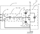
- FIG. 1 is a side view showing an outline of a switching module according to a first embodiment, which is a typical example of the present invention.
- the switching module shown in the present specification can be applied to a high frequency power supply for a semiconductor manufacturing apparatus or the like. At this time, an amplifier output of 1 kW or more and an output frequency of 0.3 MHz or more can be exemplified.
- the switching module 100 electrically connects the substrate 110, the MOSFET 120 mounted on the substrate 110, the driver circuit 130, and the damping adjustment element 140, and these elements. Includes wires 150, 152, and the like. Note that FIG. 1 shows only the path connected to the gate electrode G of the MOSFET 120, and the path connected to the drain electrode D and the source electrode S to form a part of the amplifier is not shown.
- the substrate 110 is formed as a flat plate-like member on which the MOSFET 120, the driver circuit 130, and the damping adjusting element 140 are mounted on the upper surface.
- the substrate 110 is made of a material having good thermal conductivity such as beryllium oxide (BeO) or aluminum nitride (AlN). As a result, the heat generated when the module is driven can be effectively dissipated or discharged.
- BeO beryllium oxide
- AlN aluminum nitride
- the MOSFET 120 is a kind of field effect transistor.
- an oxide film as an insulating layer and a gate electrode G are laminated on a substrate such as silicon, and a high concentration of impurities are ion-implanted to drain the MOSFET 120.
- An element configured as a semiconductor element in which the electrode D and the source electrode S are formed is used.
- any MOSFET element generally referred to as p-type or n-type can be applied.
- the driver circuit 130 has a structure including a drive power supply and a switching mechanism (not shown), and is configured to apply a predetermined gate drive voltage to the gate electrode G of the MOSFET 120 by turning on / off the switching mechanism. There is.
- As the driver circuit 130 an IC chip having a push-pull circuit composed of transistors and MOSFETs in the output stage can be exemplified.
- the damping adjusting element 140 is arranged between the MOSFET 120 and the driver circuit 130 on the substrate 110, and is electrically connected to the MOSFET 120 and the driver circuit 130 via the bonding wires 150 and 152, respectively.
- the damping adjusting element 140 is configured as, for example, a gate resistance Rg.
- the resistance value of the gate resistance Rg included therein is selected based on the parasitic capacitance of the MOSFET 120 as described later, so that the gate source voltage Vgs applied from the gate electrode G can be selected.
- the damping voltage (return voltage) Vgs1 is set as a value that does not exceed a predetermined threshold value. That is, the damping factor of the damping voltage (return voltage) Vgs1 with respect to the output voltage of the driver circuit 130 is controlled by appropriately adjusting the resistance value of the gate resistance Rg of the damping adjusting element 140.
- bonding wires 150 and 152 for example, wires made of gold, copper or aluminum are applied.
- the bonding wires 150 and 152 shown in FIG. 1 are bonded to each element by a known method such as ball bonding or wedge bonding.
- the damping adjusting element 140 can be freely replaced according to the type of the MOSFET 120 and the output frequency used.
- FIG. 2 is a circuit diagram showing an equivalent connection circuit in the vicinity of the module when the switching module according to the first embodiment is applied to an amplifier of a high frequency power supply device.
- FIG. 2 illustrates the case where the voltage input Vin and the ground GND are connected to the MOSFET 120, but the illustration and description of the equivalent connection circuit according to another configuration of the high frequency power supply device will be omitted.
- a MOSFET 120 and a driver circuit 130 are mounted on the substrate 110, and a damping adjusting element 140 and bonding wires 150 and 152 are electrically connected and arranged between the MOSFET 120 and the driver circuit 130. Therefore, a connection circuit from the driver circuit 130 to the MOSFET 120 is formed.
- the damping adjusting element 140 shown in FIG. 1 is simulated as a gate resistance Rg
- the bonding wires 150 and 152 are simulated as a configuration including a stray inductance Ls and a resistance component Rs internally.
- the driver circuit 130 includes a driver Dr, and the driver Dr is connected to the bonding wires 150 and 152 and also connected to the ground GND. Then, due to the output voltage from the driver circuit 130, a gate-source voltage Vgs corresponding to the operation of the switching mechanism described above is applied between the gate electrode G and the source electrode S of the MOSFET 120.
- FIG. 3 is a perspective view showing a typical example of the damping adjusting element shown in FIG. 1 and a modified example thereof.
- the damping adjusting element 140 is composed of a metal member 142 having a thickness H1, a length L1 in the element arrangement direction, and a width W1.
- the thickness H1 and the width W1 of the metal member 142 while fixing the length L1, the distance between the metal member 142 and the lengths of the bonding wires 150 and 152 are kept constant, and then the damping adjusting element is used.
- the gate resistance Rg of 140 can be adjusted.
- a commercially available electric resistor may be used instead of the metal member 142.
- a resistor 146 having a thickness H2, a length L2 in the element arrangement direction, and a width W2 is laminated on one surface of the base member 144. It is also possible to apply a high power chip resistor, a thin film printing resistor, or the like in which these are integrated by a protective body 148. Also in these configurations, by changing the thickness H2 and the width W2 of the resistor 146 while fixing the length L2, the distance from each element and the lengths of the bonding wires 150 and 152 are kept constant, and then the lengths are kept constant. The gate resistance Rg of the damping adjusting element 140 can be adjusted.
- the resistance value of the gate resistance Rg of the damping adjusting element 140 is determined by the following procedure based on the parasitic capacitance of the MOSFET 120 as an example. ..
- the MOSFET 120 has a parasitic capacitance. Then, among the parasitic capacitances, the input capacitance Ciss is defined as the following equation 1 using the gate-source capacitance Cgs and the gate-drain capacitance Cgd.
- the bonding wires 150 and 152 are suspended.
- the inductance Ls, the resistance component Rs, the gate resistance Rg of the damping adjusting element 140, and the gate-source capacitance Cgs of the MOSFET 120 constitute a series resonant circuit. It is known that when series resonance occurs in this series resonance circuit, the amplitude of the gate source voltage Vgs is attenuated based on the damping constant ⁇ represented by the following equation 2.
- the MOSFET 120 is turned on when the gate source voltage Vgs is applied and the voltage value exceeds a predetermined value, but even when the switching control of the driver circuit 130 is turned off, the gate source voltage Vgs Does not switch instantly, and a so-called damping voltage (return voltage) occurs.
- the gate-source voltage Vgs1 one cycle after the gate-source voltage Vgs from the driver circuit 130 is turned off can be calculated from the following equation 3 assuming that the output voltage of the driver circuit 130 is Vdr.
- the MOSFET 120 is turned on as if the signal of the on command was input, and turned on when it should be turned off. A malfunction (erroneous arc) will occur. Therefore, in order to prevent such an erroneous arc of the MOSFET 120, the gate source voltage Vgs1 after one cycle must be smaller than the above-mentioned predetermined threshold value (threshold voltage at which the MOSFET 120 is turned on) Vth. Desired. That is, the resistance value of the gate resistance Rg may be determined so that Vgs1 shown in Equation 3 has a damping constant ⁇ that is smaller than the threshold value Vth.
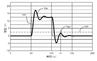
- FIG. 4 is a graph showing the time change of the voltage when a gate pulse is applied to the gate electrode using the switching module according to the first embodiment.
- the output voltage Vdr due to the gate pulse in the driver circuit 130 is shown by a dotted line, and the gate electrode G actually applies to the gate electrode G.
- the source voltage Vgs is as shown by the solid line.
- the gate source voltage after one cycle at time t1 that is, the damping voltage (return voltage) Vgs1 is generated.
- the damping constant ⁇ can be adjusted by adjusting the resistance value of the gate resistance Rg, and as a result, the damping rate of the damping voltage (return voltage) Vgs1 can be controlled.
- the switching module 100 electrically connects the driver circuit 130 and the MOSFET 120 via the bonding wires 150 and 152 and the damping adjusting element 140.
- the damping voltage (return voltage) Vgs1 of the gate source voltage can be adjusted by the gate resistance Rg of the damping adjusting element 140, and as a result, the MOSFET and the driver circuit can be adjusted. It is possible to suppress the occurrence of malfunction due to the damping voltage in the connection circuit with.
- Example 2 Generally, in MOSFET, it is known that the gate electrode G and other electrodes (drain electrode D and source electrode S) are insulated by an oxide film, and that a parasitic capacitance exists due to the capacitance of the oxide film. Has been done. This parasitic capacitance is in an inversely proportional relationship with the frequency of the MOSFET used (that is, it is desirable that the parasitic capacitance is smaller as the MOSFET frequency increases), and therefore, in the design of the amplifier, , A MOSFET suitable for this will be selected according to the output frequency.
- the bonding wire connecting the driver and the MOSFET has a stray inductance Ls and a resistance component Rs.
- These stray inductance Ls and resistance component Rs may form an RLC series circuit with the gate-source capacitance Cgs of the above-mentioned parasitic capacitances to cause a series resonance, which causes an excess in the circuit. There is a problem that a large amount of current flows.
- FIG. 5 is a circuit diagram showing an equivalent connection circuit in the vicinity of the module when the switching module according to the second embodiment is applied to an amplifier of a high frequency power supply device.
- the switching module 200 according to the second embodiment those having the same or the same configuration as that of the first embodiment are designated by the same reference numerals as those of the first embodiment, and the description thereof will be omitted again.
- the MOSFET 120 and the driver circuit 130 are mounted on the substrate 110, and the damping adjusting element 240 and the bonding wire 150 are sandwiched between the MOSFET 120 and the driver circuit 130.
- the 152 is electrically connected and arranged to form a connection circuit from the driver circuit 130 to the MOSFET 120.
- FIG. 5 the case where the voltage input Vin and the ground GND are connected to the MOSFET 120 is illustrated as in the case of the first embodiment, and the illustration and description of the equivalent connection circuit according to the other configuration of the high frequency power supply device are omitted. ..
- the damping adjusting element 240 is configured as a vibration suppression circuit including an RL parallel circuit in which the gate resistance Rg and the gate inductance Lg are connected in parallel.
- the gate resistance Rg shown in FIG. 5 the one having the same configuration as that used in Example 1 is applied.
- the inductance value changes by changing the number of turns of the gate inductance Lg.
- the resonance frequency of the connection circuit from the driver circuit 130 to the MOSFET 120 is represented by a function of the gate resistance Rg and the gate inductance Lg as described above, when the inductance value of the gate inductance Lg changes, the resonance frequency of the connection circuit Also changes. As a result, the resonance frequency in the connection circuit can be freely adjusted, so that the series resonance in the RLC series circuit formed by the connection circuit from the driver circuit 130 to the MOSFET 120 can be suppressed.
- FIG. 6 is a circuit diagram showing an equivalent connection circuit in the vicinity of the module when the switching module according to the modified example of the second embodiment is applied to the amplifier of the high frequency power supply device.
- the switching module 200 shown in FIG. 6 having the same or the same configuration as that of the first embodiment will be described again with the same reference numerals as those of the first embodiment. Omit.
- the damping adjusting element 240' is configured as a vibration suppression circuit including an RC series circuit in which the gate resistor Rg and the gate capacitor Cg are connected in series.
- Such an RC series circuit constitutes a vibration absorption circuit together with the stray inductance Ls included in the bonding wires 150 and 152.
- the gate resistance Rg shown in FIG. 6 the same configuration as that used in the first embodiment is applied.
- the damping adjusting element 240'in this configuration is a device of each element according to the resistance value of the gate resistance Rg and the capacitance value of the gate capacitor Cg. It has the function of changing the voltage applied to both ends.
- the capacitance value changes by changing the area and spacing of the electrode plate of the gate capacitor Cg.
- the resonance frequency of the connection circuit from the driver circuit 130 to the MOSFET 120 is represented by a function of the stray inductance Ls and the gate capacitor Cg. Therefore, when the capacitance value of the gate capacitor Cg changes, the resonance frequency of the connection circuit Also changes. As a result, the resonance frequency in the connection circuit can be freely adjusted as in the case shown in FIG. 5, so that the series resonance in the RLC series circuit formed by the connection circuit from the driver circuit 130 to the MOSFET 120 can be suppressed.
- the switching module 200 is configured by configuring the damping adjusting elements 240 and 240'as a vibration suppression circuit including the gate resistance Rg inside, so that the switching module 200 is parallel to or parallel to the gate resistance Rg.
- the damping adjusting elements 240 and 240' have a function as a damping resistor by the gate resistor Rg, and the connection from the driver circuit 130 to the MOSFET 120 is provided. It is also possible to have a function of freely adjusting the resonance frequency in the circuit.
- Switching module 110 Board 120 MOSFET 130 Driver circuit 140 Damping adjustment element 142 Metal member 144 Base member 146 Resistor 148 Protective body 150, 152 Bonding wire 200 Switching module 240, 240 ′ Damping adjustment element G Gate electrode D Drain electrode S Source electrode Dr Driver Rg Gate resistance Lg Gate Induction Cg Gate capacitor Vgs Gate source voltage Vgs1 Damping voltage (return voltage)
Abstract
Description
図1は、本発明の代表的な一例である実施例1によるスイッチングモジュールの概要を示す側面図である。ここで、本願明細書において示すスイッチングモジュールは、半導体製造装置向けの高周波電源等に適用できる。このとき、増幅器の出力が1kW以上で、出力周波数が0.3MHz以上のものが例示できる。 <Example 1>
FIG. 1 is a side view showing an outline of a switching module according to a first embodiment, which is a typical example of the present invention. Here, the switching module shown in the present specification can be applied to a high frequency power supply for a semiconductor manufacturing apparatus or the like. At this time, an amplifier output of 1 kW or more and an output frequency of 0.3 MHz or more can be exemplified.
一般に、MOSFETにおいては、ゲート電極Gとその他の電極(ドレイン電極D及びソース電極S)との間は酸化膜で絶縁されており、その酸化膜の静電容量により寄生容量が存在することが知られている。この寄生容量は、使用するMOSFETの周波数との間で、その適用範囲が反比例する関係(すなわち、MOSFETの周波数が大きくなると寄生容量が小さい方が望ましい)にあり、このため、増幅器の設計においては、出力する周波数に合わせてこれに適したMOSFETを選択することとなる。 <Example 2>
Generally, in MOSFET, it is known that the gate electrode G and other electrodes (drain electrode D and source electrode S) are insulated by an oxide film, and that a parasitic capacitance exists due to the capacitance of the oxide film. Has been done. This parasitic capacitance is in an inversely proportional relationship with the frequency of the MOSFET used (that is, it is desirable that the parasitic capacitance is smaller as the MOSFET frequency increases), and therefore, in the design of the amplifier, , A MOSFET suitable for this will be selected according to the output frequency.
110 基板
120 MOSFET
130 ドライバ回路
140 ダンピング調整素子
142 金属部材
144 ベース部材
146 抵抗体
148 保護体
150、152 ボンディングワイヤ
200 スイッチングモジュール
240、240´ ダンピング調整素子
G ゲート電極
D ドレイン電極
S ソース電極
Dr ドライバ
Rg ゲート抵抗
Lg ゲートインダクタンス
Cg ゲートキャパシタ
Vgs ゲート・ソース電圧
Vgs1 ダンピング電圧(戻り電圧) 100
130
Claims (5)
- MOSFETと、このMOSFETのゲート電極にゲート駆動電圧を印加するドライバ回路と、を基板上に実装したスイッチングモジュールであって、
前記ドライバ回路は、前記ゲート電極との間にダンピング調整素子及びボンディングワイヤを介して、前記MOSFETと電気的に接続されていることを特徴とするスイッチングモジュール。 A switching module in which a MOSFET and a driver circuit that applies a gate drive voltage to the gate electrode of this MOSFET are mounted on a substrate.
The driver circuit is a switching module characterized in that it is electrically connected to the MOSFET via a damping adjusting element and a bonding wire between the driver circuit and the gate electrode. - 前記ダンピング調整素子は、前記MOSFETの寄生容量に基づいてその抵抗値が設定されたゲート抵抗であることを特徴とする請求項1に記載のスイッチングモジュール。 The switching module according to claim 1, wherein the damping adjusting element is a gate resistor whose resistance value is set based on the parasitic capacitance of the MOSFET.
- 前記ゲート抵抗は、高電力チップ抵抗又は薄膜抵抗器であることを特徴とする請求項2に記載のスイッチングモジュール。 The switching module according to claim 2, wherein the gate resistor is a high power chip resistor or a thin film resistor.
- 前記ゲート抵抗の抵抗値は、前記ドライバ回路からのゲート駆動電圧の印加が終了した後の戻り電圧がしきい値を超えないように設定されることを特徴とする請求項2又は3に記載のスイッチングモジュール。 The resistance value of the gate resistor is set according to claim 2 or 3, wherein the return voltage after the application of the gate drive voltage from the driver circuit is completed is set so as not to exceed the threshold value. Switching module.
- 前記基板は、酸化ベリリウム又は窒化アルミニウムにより形成されていることを特徴とする請求項1~4のいずれか1項に記載のスイッチングモジュール。 The switching module according to any one of claims 1 to 4, wherein the substrate is made of beryllium oxide or aluminum nitride.
Priority Applications (4)
| Application Number | Priority Date | Filing Date | Title |
|---|---|---|---|
| EP19949065.7A EP4047818A4 (en) | 2019-10-15 | 2019-10-30 | Switching module |
| KR1020227008370A KR20220046650A (en) | 2019-10-15 | 2019-10-30 | switching module |
| US17/769,072 US20240113667A1 (en) | 2019-10-15 | 2019-10-30 | Switching module |
| CN201980101404.0A CN114586281A (en) | 2019-10-15 | 2019-10-30 | Switch module |
Applications Claiming Priority (2)
| Application Number | Priority Date | Filing Date | Title |
|---|---|---|---|
| JP2019-188936 | 2019-10-15 | ||
| JP2019188936A JP6772355B1 (en) | 2019-10-15 | 2019-10-15 | Switching module |
Publications (1)
| Publication Number | Publication Date |
|---|---|
| WO2021075064A1 true WO2021075064A1 (en) | 2021-04-22 |
Family
ID=72829239
Family Applications (1)
| Application Number | Title | Priority Date | Filing Date |
|---|---|---|---|
| PCT/JP2019/042558 WO2021075064A1 (en) | 2019-10-15 | 2019-10-30 | Switching module |
Country Status (7)
| Country | Link |
|---|---|
| US (1) | US20240113667A1 (en) |
| EP (1) | EP4047818A4 (en) |
| JP (1) | JP6772355B1 (en) |
| KR (1) | KR20220046650A (en) |
| CN (1) | CN114586281A (en) |
| TW (1) | TWI808352B (en) |
| WO (1) | WO2021075064A1 (en) |
Families Citing this family (1)
| Publication number | Priority date | Publication date | Assignee | Title |
|---|---|---|---|---|
| JP2022081242A (en) * | 2020-11-19 | 2022-05-31 | 株式会社京三製作所 | Switching module |
Citations (4)
| Publication number | Priority date | Publication date | Assignee | Title |
|---|---|---|---|---|
| JP2006025567A (en) | 2004-07-09 | 2006-01-26 | Renesas Technology Corp | Semiconductor device, dc-dc converter, and power supply system |
| JP2008228304A (en) | 2007-03-09 | 2008-09-25 | Huettinger Elektronik Gmbh & Co Kg | Class d amplifier device |
| JP2017092057A (en) * | 2015-11-02 | 2017-05-25 | コニカミノルタ株式会社 | Semiconductor integrated circuit and image forming apparatus |
| JP2018107494A (en) * | 2016-12-22 | 2018-07-05 | ルネサスエレクトロニクス株式会社 | Semiconductor device and inverter system |
Family Cites Families (2)
| Publication number | Priority date | Publication date | Assignee | Title |
|---|---|---|---|---|
| ATE339013T1 (en) * | 2002-01-29 | 2006-09-15 | Advanced Power Technology | SPLIT GATE POWER MODULE AND METHOD FOR SUPPRESSING VIBRATIONS THEREIN |
| JP5783997B2 (en) * | 2012-12-28 | 2015-09-24 | 三菱電機株式会社 | Power semiconductor device |
-
2019
- 2019-10-15 JP JP2019188936A patent/JP6772355B1/en active Active
- 2019-10-30 EP EP19949065.7A patent/EP4047818A4/en active Pending
- 2019-10-30 US US17/769,072 patent/US20240113667A1/en active Pending
- 2019-10-30 KR KR1020227008370A patent/KR20220046650A/en not_active Application Discontinuation
- 2019-10-30 WO PCT/JP2019/042558 patent/WO2021075064A1/en active Application Filing
- 2019-10-30 CN CN201980101404.0A patent/CN114586281A/en active Pending
-
2020
- 2020-10-14 TW TW109135433A patent/TWI808352B/en active
Patent Citations (4)
| Publication number | Priority date | Publication date | Assignee | Title |
|---|---|---|---|---|
| JP2006025567A (en) | 2004-07-09 | 2006-01-26 | Renesas Technology Corp | Semiconductor device, dc-dc converter, and power supply system |
| JP2008228304A (en) | 2007-03-09 | 2008-09-25 | Huettinger Elektronik Gmbh & Co Kg | Class d amplifier device |
| JP2017092057A (en) * | 2015-11-02 | 2017-05-25 | コニカミノルタ株式会社 | Semiconductor integrated circuit and image forming apparatus |
| JP2018107494A (en) * | 2016-12-22 | 2018-07-05 | ルネサスエレクトロニクス株式会社 | Semiconductor device and inverter system |
Non-Patent Citations (1)
| Title |
|---|
| See also references of EP4047818A4 |
Also Published As
| Publication number | Publication date |
|---|---|
| TW202121816A (en) | 2021-06-01 |
| CN114586281A (en) | 2022-06-03 |
| JP2021064889A (en) | 2021-04-22 |
| JP6772355B1 (en) | 2020-10-21 |
| EP4047818A4 (en) | 2023-11-22 |
| KR20220046650A (en) | 2022-04-14 |
| US20240113667A1 (en) | 2024-04-04 |
| TWI808352B (en) | 2023-07-11 |
| EP4047818A1 (en) | 2022-08-24 |
Similar Documents
| Publication | Publication Date | Title |
|---|---|---|
| US10607978B2 (en) | Semiconductor device and electronic apparatus | |
| US9741702B2 (en) | Semiconductor power modules and devices | |
| JP5783997B2 (en) | Power semiconductor device | |
| JP5858914B2 (en) | Power module and output circuit | |
| JP6184137B2 (en) | Power management chip and power management apparatus including the same | |
| US8461881B2 (en) | High power, high speed solid state relay | |
| US20050213308A1 (en) | Hybrid integrated circuit device | |
| JP5925364B2 (en) | Power semiconductor device | |
| US10826487B2 (en) | Power unit with an integrated pull-down transistor | |
| JP2014099535A (en) | Semiconductor device | |
| CN109768787B (en) | Semiconductor device and driving method thereof | |
| JP6772355B1 (en) | Switching module | |
| US20190181078A1 (en) | Semiconductor package | |
| KR100846880B1 (en) | Gate driver output stage with bias circuit for high and wide operating voltage range | |
| WO2020152036A1 (en) | Power module comprising an active miller clamp | |
| JP5359264B2 (en) | Semiconductor device | |
| WO2022107375A1 (en) | Switching module | |
| US6809387B2 (en) | Power switching device | |
| US20210167770A1 (en) | Semiconductor module | |
| WO2021145133A1 (en) | Power supply device, acf converter, and ac adapter | |
| JP5577296B2 (en) | Semiconductor device | |
| TWM643423U (en) | GaN HIGH ELECTRON MOBILITY TRANSISTOR SWITCH CHIP | |
| JP2017093239A (en) | Electric power conversion system with switch element comprised of wide-gap semiconductor | |
| JP2024039516A (en) | Semiconductor devices and switching circuits | |
| CN117501446A (en) | Semiconductor device with a semiconductor device having a plurality of semiconductor chips |
Legal Events
| Date | Code | Title | Description |
|---|---|---|---|
| 121 | Ep: the epo has been informed by wipo that ep was designated in this application |
Ref document number: 19949065 Country of ref document: EP Kind code of ref document: A1 |
|
| ENP | Entry into the national phase |
Ref document number: 20227008370 Country of ref document: KR Kind code of ref document: A |
|
| WWE | Wipo information: entry into national phase |
Ref document number: 17769072 Country of ref document: US |
|
| NENP | Non-entry into the national phase |
Ref country code: DE |
|
| ENP | Entry into the national phase |
Ref document number: 2019949065 Country of ref document: EP Effective date: 20220516 |