WO2021070506A1 - Dc/dc converter - Google Patents
Dc/dc converter Download PDFInfo
- Publication number
- WO2021070506A1 WO2021070506A1 PCT/JP2020/032564 JP2020032564W WO2021070506A1 WO 2021070506 A1 WO2021070506 A1 WO 2021070506A1 JP 2020032564 W JP2020032564 W JP 2020032564W WO 2021070506 A1 WO2021070506 A1 WO 2021070506A1
- Authority
- WO
- WIPO (PCT)
- Prior art keywords
- switch
- conductive path
- control
- state
- capacitor
- Prior art date
Links
- 239000003990 capacitor Substances 0.000 claims abstract description 151
- 238000006243 chemical reaction Methods 0.000 claims description 129
- HEZMWWAKWCSUCB-PHDIDXHHSA-N (3R,4R)-3,4-dihydroxycyclohexa-1,5-diene-1-carboxylic acid Chemical compound O[C@@H]1C=CC(C(O)=O)=C[C@H]1O HEZMWWAKWCSUCB-PHDIDXHHSA-N 0.000 claims description 109
- 239000004065 semiconductor Substances 0.000 claims description 95
- 239000003985 ceramic capacitor Substances 0.000 claims description 11
- 238000001514 detection method Methods 0.000 description 46
- 230000003071 parasitic effect Effects 0.000 description 12
- 230000002457 bidirectional effect Effects 0.000 description 5
- 238000010586 diagram Methods 0.000 description 3
- 230000000694 effects Effects 0.000 description 3
- 238000000034 method Methods 0.000 description 3
- HBBGRARXTFLTSG-UHFFFAOYSA-N Lithium ion Chemical compound [Li+] HBBGRARXTFLTSG-UHFFFAOYSA-N 0.000 description 2
- 229910001416 lithium ion Inorganic materials 0.000 description 2
- 238000012986 modification Methods 0.000 description 1
- 230000004048 modification Effects 0.000 description 1
Images
Classifications
-
- H—ELECTRICITY
- H02—GENERATION; CONVERSION OR DISTRIBUTION OF ELECTRIC POWER
- H02M—APPARATUS FOR CONVERSION BETWEEN AC AND AC, BETWEEN AC AND DC, OR BETWEEN DC AND DC, AND FOR USE WITH MAINS OR SIMILAR POWER SUPPLY SYSTEMS; CONVERSION OF DC OR AC INPUT POWER INTO SURGE OUTPUT POWER; CONTROL OR REGULATION THEREOF
- H02M1/00—Details of apparatus for conversion
- H02M1/32—Means for protecting converters other than automatic disconnection
- H02M1/322—Means for rapidly discharging a capacitor of the converter for protecting electrical components or for preventing electrical shock
-
- H—ELECTRICITY
- H02—GENERATION; CONVERSION OR DISTRIBUTION OF ELECTRIC POWER
- H02M—APPARATUS FOR CONVERSION BETWEEN AC AND AC, BETWEEN AC AND DC, OR BETWEEN DC AND DC, AND FOR USE WITH MAINS OR SIMILAR POWER SUPPLY SYSTEMS; CONVERSION OF DC OR AC INPUT POWER INTO SURGE OUTPUT POWER; CONTROL OR REGULATION THEREOF
- H02M3/00—Conversion of dc power input into dc power output
- H02M3/02—Conversion of dc power input into dc power output without intermediate conversion into ac
- H02M3/04—Conversion of dc power input into dc power output without intermediate conversion into ac by static converters
- H02M3/10—Conversion of dc power input into dc power output without intermediate conversion into ac by static converters using discharge tubes with control electrode or semiconductor devices with control electrode
- H02M3/145—Conversion of dc power input into dc power output without intermediate conversion into ac by static converters using discharge tubes with control electrode or semiconductor devices with control electrode using devices of a triode or transistor type requiring continuous application of a control signal
- H02M3/155—Conversion of dc power input into dc power output without intermediate conversion into ac by static converters using discharge tubes with control electrode or semiconductor devices with control electrode using devices of a triode or transistor type requiring continuous application of a control signal using semiconductor devices only
- H02M3/156—Conversion of dc power input into dc power output without intermediate conversion into ac by static converters using discharge tubes with control electrode or semiconductor devices with control electrode using devices of a triode or transistor type requiring continuous application of a control signal using semiconductor devices only with automatic control of output voltage or current, e.g. switching regulators
-
- H—ELECTRICITY
- H02—GENERATION; CONVERSION OR DISTRIBUTION OF ELECTRIC POWER
- H02M—APPARATUS FOR CONVERSION BETWEEN AC AND AC, BETWEEN AC AND DC, OR BETWEEN DC AND DC, AND FOR USE WITH MAINS OR SIMILAR POWER SUPPLY SYSTEMS; CONVERSION OF DC OR AC INPUT POWER INTO SURGE OUTPUT POWER; CONTROL OR REGULATION THEREOF
- H02M1/00—Details of apparatus for conversion
- H02M1/32—Means for protecting converters other than automatic disconnection
-
- H—ELECTRICITY
- H02—GENERATION; CONVERSION OR DISTRIBUTION OF ELECTRIC POWER
- H02M—APPARATUS FOR CONVERSION BETWEEN AC AND AC, BETWEEN AC AND DC, OR BETWEEN DC AND DC, AND FOR USE WITH MAINS OR SIMILAR POWER SUPPLY SYSTEMS; CONVERSION OF DC OR AC INPUT POWER INTO SURGE OUTPUT POWER; CONTROL OR REGULATION THEREOF
- H02M1/00—Details of apparatus for conversion
- H02M1/36—Means for starting or stopping converters
-
- H—ELECTRICITY
- H02—GENERATION; CONVERSION OR DISTRIBUTION OF ELECTRIC POWER
- H02M—APPARATUS FOR CONVERSION BETWEEN AC AND AC, BETWEEN AC AND DC, OR BETWEEN DC AND DC, AND FOR USE WITH MAINS OR SIMILAR POWER SUPPLY SYSTEMS; CONVERSION OF DC OR AC INPUT POWER INTO SURGE OUTPUT POWER; CONTROL OR REGULATION THEREOF
- H02M3/00—Conversion of dc power input into dc power output
- H02M3/02—Conversion of dc power input into dc power output without intermediate conversion into ac
- H02M3/04—Conversion of dc power input into dc power output without intermediate conversion into ac by static converters
- H02M3/10—Conversion of dc power input into dc power output without intermediate conversion into ac by static converters using discharge tubes with control electrode or semiconductor devices with control electrode
- H02M3/145—Conversion of dc power input into dc power output without intermediate conversion into ac by static converters using discharge tubes with control electrode or semiconductor devices with control electrode using devices of a triode or transistor type requiring continuous application of a control signal
- H02M3/155—Conversion of dc power input into dc power output without intermediate conversion into ac by static converters using discharge tubes with control electrode or semiconductor devices with control electrode using devices of a triode or transistor type requiring continuous application of a control signal using semiconductor devices only
- H02M3/156—Conversion of dc power input into dc power output without intermediate conversion into ac by static converters using discharge tubes with control electrode or semiconductor devices with control electrode using devices of a triode or transistor type requiring continuous application of a control signal using semiconductor devices only with automatic control of output voltage or current, e.g. switching regulators
- H02M3/158—Conversion of dc power input into dc power output without intermediate conversion into ac by static converters using discharge tubes with control electrode or semiconductor devices with control electrode using devices of a triode or transistor type requiring continuous application of a control signal using semiconductor devices only with automatic control of output voltage or current, e.g. switching regulators including plural semiconductor devices as final control devices for a single load
- H02M3/1582—Buck-boost converters
-
- H—ELECTRICITY
- H02—GENERATION; CONVERSION OR DISTRIBUTION OF ELECTRIC POWER
- H02M—APPARATUS FOR CONVERSION BETWEEN AC AND AC, BETWEEN AC AND DC, OR BETWEEN DC AND DC, AND FOR USE WITH MAINS OR SIMILAR POWER SUPPLY SYSTEMS; CONVERSION OF DC OR AC INPUT POWER INTO SURGE OUTPUT POWER; CONTROL OR REGULATION THEREOF
- H02M3/00—Conversion of dc power input into dc power output
- H02M3/22—Conversion of dc power input into dc power output with intermediate conversion into ac
- H02M3/24—Conversion of dc power input into dc power output with intermediate conversion into ac by static converters
- H02M3/28—Conversion of dc power input into dc power output with intermediate conversion into ac by static converters using discharge tubes with control electrode or semiconductor devices with control electrode to produce the intermediate ac
- H02M3/325—Conversion of dc power input into dc power output with intermediate conversion into ac by static converters using discharge tubes with control electrode or semiconductor devices with control electrode to produce the intermediate ac using devices of a triode or a transistor type requiring continuous application of a control signal
- H02M3/335—Conversion of dc power input into dc power output with intermediate conversion into ac by static converters using discharge tubes with control electrode or semiconductor devices with control electrode to produce the intermediate ac using devices of a triode or a transistor type requiring continuous application of a control signal using semiconductor devices only
- H02M3/33569—Conversion of dc power input into dc power output with intermediate conversion into ac by static converters using discharge tubes with control electrode or semiconductor devices with control electrode to produce the intermediate ac using devices of a triode or a transistor type requiring continuous application of a control signal using semiconductor devices only having several active switching elements
- H02M3/33576—Conversion of dc power input into dc power output with intermediate conversion into ac by static converters using discharge tubes with control electrode or semiconductor devices with control electrode to produce the intermediate ac using devices of a triode or a transistor type requiring continuous application of a control signal using semiconductor devices only having several active switching elements having at least one active switching element at the secondary side of an isolation transformer
- H02M3/33584—Bidirectional converters
Definitions
- This disclosure relates to a DCDC converter.
- a DCDC converter is provided with a capacitor in a conductive path on the input side or an output side.
- a capacitor in a conductive path on the input side or an output side.
- an input side capacitor is electrically connected to an input side conductive path
- an output side capacitor is electrically connected to an output side conductive path.
- a DCDC converter has been proposed in which a cutoff switch is provided in a conductive path on the input side or a conductive path on the output side assuming a short circuit failure of a circuit.
- This type of DCDC converter may adopt a configuration in which a cutoff switch is interposed between an external power supply provided on the input side or the output side and a capacitor electrically connected to the conductive path.
- a cutoff switch is interposed between the external power supply provided on the input side or the output side and a capacitor electrically connected to the conductive path.
- a large inrush current is applied to the capacitor in response to the switch to the on state. Easy to flow.
- the DCDC converter in which a switch is interposed between the external power supply and the capacitor is not limited to the above example, and the same problem may occur in any of the examples.
- the present disclosure provides a technique capable of suppressing the inrush current flowing into the capacitor in the DCDC converter.
- the DCDC converter is A voltage conversion unit provided between the first conductive path and the second conductive path, A capacitor provided between the conductive path of either the first conductive path or the second conductive path and the reference conductive path, and A switch between the external power supply and the capacitor, A control unit that switches the switch between an on state and an off state, With When the switch is in the off state, the flow of current from the external power supply to the capacitor is cut off, and at least when the switch is in the on state, the external power supply is sent to the capacitor via the one conductive path. And current is allowed to flow, The control unit intermittently turns the switch on intermittently before the energization control when switching from the cutoff control that keeps the switch in the off state to the energization control that keeps the switch in the on state. I do.
- the DCDC converter of one aspect of the present disclosure can suppress the inrush current flowing into the capacitor.
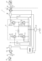
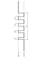
- FIG. 1 is a circuit diagram showing a DCDC converter according to the first embodiment.
- FIG. 2 is a time chart showing an example of the waveform of the drive signal output from the control unit in the first intermittent control and the second intermittent control to the first cutoff switch and the second cutoff switch in the DCDC converter of the first embodiment. is there.
- FIG. 3 shows the path of the current flowing from the second external power supply to the second capacitor when the second cutoff switch is on during the execution of the second intermittent control and the execution of the first intermittent control in the DCDC converter of the first embodiment. It is a circuit diagram which shows the path of the current which flows from the 1st external power source to the 1st capacitor when the 1st cutoff switch is turned on.
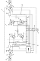
- FIG. 4 is a circuit diagram showing the DCDC converter of the second embodiment.
- FIG. 5 is an example of the waveform of the drive signal output from the control unit in the intermittent control to the first cutoff switch, the second cutoff switch, and the semiconductor switch in the DCDC converter of another embodiment.
- the DCDC converter of one aspect of the present disclosure includes a voltage conversion unit, a capacitor, a switch, and a control unit.
- the voltage conversion unit is provided between the first conductive path and the second conductive path.
- the capacitor is provided between the conductive path of either the first conductive path or the second conductive path and the reference conductive path.
- the switch is located between the external power supply and the capacitor.
- the control unit switches the switch between the on state and the off state. When the switch is off, the current flow from the external power supply to the capacitor is cut off. It is permissible for current to flow from the external power supply into the capacitor through one of the conductive paths, at least when the switch is on.
- the control unit performs intermittent control in which the switch is intermittently turned on before the energization control when switching from the cutoff control in which the switch is maintained in the off state to the energization control in which the switch is maintained in the on state.
- the DCDC converter having the configuration of (1) above executes intermittent control when the switch is switched from cutoff control to energization control, the inrush current flowing into the capacitor is suppressed as compared with the case where the energization control is started at the end timing of the cutoff control. be able to. Therefore, the DCDC converter can reduce the problem caused by the excessive inrush current flowing through the capacitor when the cutoff control is released.
- the DCDC converter described in (1) above may be a DCDC converter to which the following features are further added.
- the switch may include a cutoff switch provided between the external power supply and the voltage conversion unit in one of the conductive paths.
- the cutoff switch is configured to allow energization from the external power supply side to the voltage conversion unit side when it is on, and to cut off energization from the external power supply side to the voltage conversion unit side when it is off. It may have been done.
- the DCDC converter having the configuration of (2) above can suppress an increase in special dedicated parts and the like, and can suppress an excessive current when the cutoff control is released by using a cutoff switch required for the protection function. Therefore, this DCDC converter can suppress the inrush current to the capacitor with a simpler configuration.
- the DCDC converter described in (1) above may be a DCDC converter to which the following features are added.
- the switch is a first cutoff switch provided between the first external power supply and the voltage conversion unit in the first conductive path, and a second cutoff switch provided between the second external power supply and the voltage conversion unit in the second conductive path. It may include a switch.
- the first cutoff switch allows energization from the first external power supply side to the voltage conversion unit side when it is on, and energizes the voltage conversion unit side from the first external power supply side when it is off. Can be blocked.
- the second cutoff switch allows energization from the second external power supply side to the voltage conversion unit side when it is on, and energizes the voltage conversion unit side from the second external power supply side when it is off.
- the control unit When switching from the first cutoff control that keeps the first cutoff switch in the off state to the first energization control that keeps the first cutoff switch in the on state, the control unit interrupts the first cutoff switch before the first energization control.
- the first intermittent control that is turned on can be performed.
- the control unit intermittently interrupts the second cutoff switch before the second power supply control when switching from the second cutoff control that keeps the second cutoff switch in the off state to the second power supply control that keeps the second cutoff switch in the on state.
- the second intermittent control that is turned on can be performed.
- the DCDC converter described in (3) above can be protected by providing a cutoff switch in both the first conductive path and the second conductive path. Further, this DCDC converter suppresses the inrush current flowing from the external power supply to the capacitor even when the cutoff control is released by either the cutoff switch of the first conductive path or the second conductive path while realizing such a protection function. be able to.
- the DCDC converter according to any one of (1) to (3) above may be a DCDC converter including a semiconductor switch in which the switch forms a part of a voltage conversion unit.
- the DCDC converter described in (4) above suppresses the increase of special dedicated parts and the like, and uses a semiconductor switch necessary to realize the function of the voltage converter to reduce the excessive current when the cutoff control is released. It can be suppressed. Therefore, this DCDC converter can suppress the inrush current to the capacitor with a simpler configuration.
- the DCDC converter according to any one of (1) to (4) above may be a DCDC converter to which the following features are further added.
- the control unit may make the switch-on time in a part of the whole period of intermittent control longer than the switch-on time in the period before the part.
- the DCDC converter according to any one of (1) to (5) above may be a DCDC converter to which the following features are further added.
- the voltage conversion unit includes a drive switching element, and boosts or lowers the voltage applied to one of the first conductive path and the second conductive path according to the on / off operation of the drive switching element, and applies an output voltage to the other. Can be done.
- the control unit performs voltage conversion control for turning on / off the drive switching element, and the frequency of the on / off operation of the switch in the intermittent control may be higher than the frequency of the on / off operation of the drive switching element in the voltage conversion control.
- the frequency of the switch on / off operation during intermittent control can be made higher than the frequency of the on / off operation of the drive switching element during voltage conversion. That is, this DCDC converter can shorten each on-time during intermittent control, and can further reduce the current flowing into the capacitor at each on-time during intermittent control. Therefore, this DCDC converter can more reliably suppress the inrush current to the capacitor.
- the DCDC converter according to any one of (1) to (6) above may also be a DCDC converter in which the capacitor is a ceramic capacitor.
- Ceramic capacitors can be made smaller than electrolytic capacitors that have the same electrical characteristics. On the other hand, ceramic capacitors have a smaller internal resistance than electrolytic capacitors. Therefore, since the internal resistance is small, the ceramic capacitor tends to have a larger inrush current than the electrolytic capacitor. In the DCDC converter described in (7) above, even when a ceramic capacitor is used, the magnitude of the inrush current to the capacitor can be satisfactorily suppressed in one ON state by performing intermittent control.
- the reference conductive path is a conductive path maintained at a reference potential lower than the potential of one of the above conductive paths. Is desirable.
- control unit switches the cutoff switch to the off state when a current equal to or higher than the threshold value flows or the voltage becomes lower than the threshold value in one of the above-mentioned conductive paths.
- the DCDC converter 1 shown in FIG. 1 is configured as, for example, an in-vehicle buck-boost DCDC converter, and boosts or lowers the DC voltage applied to one of the first conductive path 91 and the second conductive path 92. Then, it is configured to output to the other conductive path.
- the DCDC converter 1 includes a first conductive path 91 and a second conductive path 92 as power lines.
- the first conductive path 91 is a wiring that is electrically connected to the terminal on the high potential side of the first external power supply 61 and conducts with the terminal on the high potential side.
- the first conductive path 91 has a configuration in which a predetermined DC voltage is applied from the first external power source 61.
- the second conductive path 92 is a wiring that is electrically connected to the terminal on the high potential side of the second external power supply 62 and conducts with the terminal on the high potential side.
- the second conductive path 92 has a configuration in which a predetermined DC voltage is applied from the second external power supply 62.
- electrically connected is preferably configured to be connected in a state of being electrically connected to each other (a state in which a current can flow) so that both potentials of the connection target are equal.
- the configuration is not limited to this.
- electrically connected may be a configuration in which both connection targets are connected in a state in which both connection targets can be electrically connected while an electric component is interposed between the two connection targets.
- the first external power supply 61 and the second external power supply 62 are composed of known power storage means such as a lead storage battery, a lithium ion battery, an electric double layer capacitor, a lithium ion capacitor, and other power storage units.
- the specific values of the output voltage of the first external power supply 61 and the output voltage of the second external power supply 62 are not particularly limited.
- the terminals on the low potential side of the first external power supply 61 and the second external power supply 62 are electrically connected to a ground portion (not shown) and maintained at a predetermined ground potential (0 V).
- the DCDC converter 1 includes a voltage conversion unit 6, a first capacitor C1, a second capacitor C2, a cutoff switch 70, a first current detection unit 81, a second current detection unit 82, a third current detection unit 83, and a first voltage detection unit. , A second voltage detection unit, and a control unit 12.
- the voltage conversion unit 6 boosts or lowers the voltage applied to one of the first conductive path 91 and the second conductive path 92 according to the on / off operation of the semiconductor switches T1, T2, T3, and T4, and applies the output voltage to the other. It has a function to apply.
- the voltage conversion unit 6 is provided between the first conductive path 91 and the second conductive path 92.
- the voltage conversion unit 6 can perform the first conversion operation and the second conversion operation. In the first conversion operation, the voltage applied to the first conductive path 91 is stepped down to apply a voltage to the second conductive path 92, or the voltage applied to the second conductive path 92 is boosted to increase the voltage applied to the first conductive path 91. At least one of the operations of applying a voltage to.
- the voltage applied to the first conductive path 91 is boosted to apply a voltage to the second conductive path 92, or the voltage applied to the second conductive path 92 is stepped down to lower the voltage applied to the first conductive path 91. At least one of the operations of applying a voltage to.
- the voltage conversion unit 6 includes semiconductor switches T1, T2, T3, and T4 arranged in an H-bridge structure and an inductor L, and functions as a DCDC converter that executes so-called bidirectional buck-boost.
- the semiconductor switches T1, T2, T3, and T4 are all configured as N-channel MOSFETs.
- the semiconductor switch T1 is a first high-side element.
- the semiconductor switch T2 is a first low-side element.
- the semiconductor switch T3 is a second high-side element.
- the semiconductor switch T4 is a second low-side element.
- the semiconductor switches T1 and T2 constitute the first switch unit S1.
- the semiconductor switches T3 and T4 form a second switch portion S2.
- Each of the semiconductor switches T1, T2, T3, and T4 is provided with parasitic diodes T11, T12, T13, and T14, which are parasitic components. Specifically, in each of the semiconductor switches T1, T2, T3, and T4, the cathodes of the parasitic diodes T11, T12, T13, and T14 are electrically connected to the drain side and the anode of each semiconductor switch to the source side. It is said that.
- the inductor L is configured as a known coil having a predetermined inductance.
- the first conductive path 91 is electrically connected to the drain of the semiconductor switch T1, and the drain of the semiconductor switch T2 and one end of the inductor L are electrically connected to the source of the semiconductor switch T1.
- the second conductive path 92 is electrically connected to the drain of the semiconductor switch T3, and the drain of the semiconductor switch T4 and the other end of the inductor L are electrically connected to the source of the semiconductor switch T3.
- Each source of the semiconductor switches T2 and T4 is electrically connected to the ground G via the reference conductive path 93.
- a drive signal such as a PWM signal is input from the control unit 12 to each gate of the semiconductor switches T1, T2, T3, and T4.
- the reference conductive path 93 is a conductive path maintained at a reference potential (ground G potential) lower than the potentials of the first conductive path 91 and the second conductive path 92.
- the first capacitor C1 is provided between the first conductive path 91 and the reference conductive path 93. Specifically, one terminal of the first capacitor C1 is electrically connected to the first conductive path 91, and the other terminal is electrically connected to the reference conductive path 93.
- the second capacitor C2 is provided between the second conductive path 92 and the reference conductive path 93. Specifically, one terminal of the second capacitor C2 is electrically connected to the second conductive path 92, and the other terminal is electrically connected to the reference conductive path 93.
- a ceramic capacitor, a film capacitor, or the like is used for the first capacitor C1 and the second capacitor C2. The internal resistance of ceramic capacitors and film capacitors tends to be smaller than that of electrolytic capacitors. An electrolytic capacitor may be used for the first capacitor C1 and the second capacitor C2.
- the cutoff switch 70 has a first cutoff switch 71 and a second cutoff switch 72.
- the first cutoff switch 71 is configured as, for example, an N-channel MOSFET. Specifically, the first cutoff switch 71 is in an on state that allows bidirectional energization of the first conductive path 91, and in the direction from the first external power source 61 toward the voltage conversion unit 6 side in the first conductive path 91. It is configured to switch to the off state, which shuts off the energization.
- the first cutoff switch 71 is interposed in the first conductive path 91, and one end side (source) is electrically connected to one terminal of the voltage conversion unit 6 and the first capacitor C1.
- the other end side (drain) of the first cutoff switch 71 is electrically connected to the first conductive path 91 on the side of the first external power supply 61, and is switched between an on state and an off state by the control unit 12. That is, the first cutoff switch 71 is provided between the first external power supply 61 and the voltage conversion unit 6 in the first conductive path 91.
- the first cutoff switch 71 is a switch S interposed between the first external power supply 61 and the first capacitor C1. When the first cutoff switch 71 is in the ON state, it allows at least energization from the first external power supply 61 to the voltage conversion unit 6 side, and also allows current to flow into the first capacitor C1. When the first cutoff switch 71 is in the off state, the first cutoff switch 71 cuts off the energization from the first external power supply 61 to the voltage conversion unit 6 side and also cuts off the current from flowing into the first capacitor C1.
- a parasitic diode 71A is electrically connected to the first cutoff switch 71. The anode of the parasitic diode 71A is electrically connected to the voltage conversion unit 6, and the cathode is electrically connected to the first conductive path 91 on the first external power supply 61 side.
- the second cutoff switch 72 is configured as, for example, an N-channel MOSFET. Specifically, the second cutoff switch 72 is in an on state that allows bidirectional energization of the second conductive path 92, and in the direction from the second external power source 62 toward the voltage conversion unit 6 side in the second conductive path 92. It is configured to switch to the off state, which shuts off the energization.
- the second cutoff switch 72 is interposed in the second conductive path 92, and one end side (source) is electrically connected to one terminal of the voltage conversion unit 6 and the second capacitor C2.
- the other end side (drain) of the second cutoff switch 72 is electrically connected to the second conductive path 92 on the second external power supply 62 side, and is switched between an on state and an off state by the control unit 12. That is, the second cutoff switch 72 is provided between the second external power supply 62 and the voltage conversion unit 6 in the second conductive path 92.
- the second cutoff switch 72 is a switch S interposed between the second external power supply 62 and the second capacitor C2. When the second cutoff switch 72 is in the ON state, it allows at least energization from the second external power supply 62 to the voltage conversion unit 6 side, and also allows current to flow into the second capacitor C2. When the second cutoff switch 72 is in the off state, the second cutoff switch 72 cuts off the energization from the second external power supply 62 to the voltage conversion unit 6 side and also cuts off the current from flowing into the second capacitor C2.
- a parasitic diode 72A is electrically connected to the second cutoff switch 72. The anode of the parasitic diode 72A is electrically connected to the voltage conversion unit 6, and the cathode is electrically connected to the second conductive path 92 on the second external power supply 62 side.
- the first current detection unit 81 is provided between the voltage conversion unit 6 and the first cutoff switch 71 in the first conductive path 91.
- the second current detection unit 82 is provided between the voltage conversion unit 6 and the second cutoff switch 72 in the second conductive path 92.
- the third current detection unit 83 is provided between the voltage conversion unit 6 and the ground G in the reference conductive path 93.
- the first current detection unit 81, the second current detection unit 82, and the third current detection unit 83 are configured as a known current detection circuit using, for example, a current transformer or a shunt resistor.
- the first voltage detection unit (not shown) outputs a value indicating the first voltage in the first conductive path 91 to the control unit 12.
- the second voltage detection unit (not shown) outputs a value indicating the second voltage in the second conductive path 92 to the control unit 12.
- the control unit 12 is configured as, for example, a microcomputer.
- the control unit 12 is known from the first voltage detection unit and the second voltage detection unit based on the value indicating the first voltage in the first conductive path 91, the value indicating the second voltage in the second conductive path 92, and the target voltage value. Feedback control is performed by the method of.
- the control unit 12 sets the duty of the PWM signal given to the voltage conversion unit 6.
- the control unit 12 outputs the set signal toward the gates of the semiconductor switches T1, T2, T3, and T4 of the voltage conversion unit 6.
- the control unit 12 performs voltage conversion control for turning on / off the semiconductor switches T1, T2, T3, and T4.
- the target voltage value may be a value set by the control unit 12 or a value instructed by an external device such as an external ECU.
- the control unit 12 when performing a first conversion operation of stepping down from the first external power supply 61 to the second external power supply 62 or stepping up from the second external power supply 62 to the first external power supply 61, the control unit 12 is the first switch.
- the voltage conversion control of unit S1 is executed.
- the control unit 12 keeps the semiconductor switch T3 in the on state and keeps the semiconductor switch T4 in the off state.
- the semiconductor switches T1 and T2 of the first switch unit S1 operate on and off by voltage conversion control, and the voltage applied to one of the first conductive path 91 and the second conductive path 92 is boosted or stepped down and output to the other. It operates as drive switching elements D1 and D2 to which a voltage is applied.
- the control unit 12 When performing a second conversion operation of stepping down from the second external power supply 62 to the first external power supply 61 or stepping up from the first external power supply 61 to the second external power supply 62, the control unit 12 uses the second switch unit S2. Performs voltage conversion control. At this time, the control unit 12 keeps the semiconductor switch T1 in the on state and keeps the semiconductor switch T2 in the off state.
- the semiconductor switches T3 and T4 of the second switch unit S2 operate on and off by voltage conversion control, and the voltage applied to one of the first conductive path 91 and the second conductive path 92 is boosted or stepped down and output to the other. It operates as drive switching elements D3 and D4 to which a voltage is applied.
- the control unit 12 receives an ignition off signal indicating that the ignition switch (not shown) provided in the vehicle is in the off state and the ignition switch is in the off state from a device (external ECU or the like) provided outside the DCDC converter 1. If input, cutoff control is executed. Specifically, at this time, the control unit 12 outputs a signal set to the L level toward each gate of the semiconductor switches T1, T2, T3, T4, the first cutoff switch 71, and the second cutoff switch 72. .. As a result, each of the semiconductor switches T1, T2, T3, T4, the first cutoff switch 71, and the second cutoff switch 72 is turned off.
- the control unit 12 maintains the semiconductor switches T1, T2, T3, T4, the first cutoff switch 71 (switch S), and the second cutoff switch 72 (switch S) in the off state by executing the cutoff control. ..
- the cutoff control by the control unit 12 for the first cutoff switch 71 is the first cutoff control
- the cutoff control by the control unit 12 for the second cutoff switch 72 is the second cutoff control.
- the first capacitor C1 and the second capacitor C2 are in an uncharged state.
- control unit 12 intermittently switches the second cutoff switch 72 before switching from the second cutoff control that keeps the second cutoff switch 72 in the off state to the second energization control that keeps the second cutoff switch 72 in the on state.
- the second intermittent control to turn on is performed.
- the H level signal is continued for P2 for a predetermined period, and then the L level signal is continued for P3 for a predetermined period.
- the control unit 12 sends an H level signal and an L level signal toward the respective gates of the first cutoff switch 71 and the second cutoff switch 72 during the period P1 in which the first intermittent control and the second intermittent control (intermittent control) are executed. Outputs alternately and repeatedly. As a result, the first cutoff switch 71 and the second cutoff switch 72 are turned on to conduct the drain and the source when the H level signal is input to the gate.
- the time P2 of the H level signal is shorter than the time of the H level signal of the PWM signal during voltage conversion control (not shown). That is, the frequency of the on / off operation of the first cutoff switch 71 (switch S) and the second cutoff switch 72 (switch S) in the first intermittent control and the second intermittent control (intermittent control) is the drive switching element D1 in the voltage conversion control. , D2, D3, D4 (semiconductor switches T1, T2, T3, T4) are higher than the on / off operation frequency.
- the second intermittent control when the second cutoff switch 72 is in the ON state, a current flows from the second external power supply 62 to the second capacitor C2 in the path shown by the arrow A2 as shown in FIG.
- the first intermittent control when the first cutoff switch 71 is in the ON state, a current flows from the first external power supply 61 to the first capacitor C1 along the path shown by the arrow A1.
- the first cutoff switch 71 and the second cutoff switch 72 are in an off state in which the drain and the source are not conductive when an L level signal is input to the gate. That is, the control unit 12 intermittently controls the first cutoff switch 71 to intermittently flow a current from the first external power supply 61 to the first capacitor C1. Then, the control unit 12 intermittently controls the second cutoff switch 72 to allow a current to flow intermittently from the second external power supply 62 to the second capacitor C2. As a result, it is possible to prevent the current (inrush current) flowing through each of the first capacitor C1 and the second capacitor C2 from becoming excessively large.
- the DCDC converter 1 has a configuration in which the first current detection unit 81 can detect the current flowing through the first conductive path 91.
- the DCDC converter 1 has a configuration in which the second current detection unit 82 can detect the current flowing through the second conductive path 92.
- the DCDC converter 1 has a configuration in which the third current detection unit 83 can detect the current flowing to the ground G via the first capacitor C1, the second capacitor C2, and the voltage conversion unit 6. Therefore, the DCDC converter 1 suppresses the current flowing through the first capacitor C1 and the second capacitor C2 from becoming excessively large, so that the first current detection unit 81, the second current detection unit 82, and the third current detection unit 83 are suppressed. It suppresses the detection of an excessively large current value.
- the conditions for terminating the first intermittent control and the second intermittent control are, for example, when the current flowing through the first capacitor C1 and the second capacitor C2 becomes smaller than a predetermined value, or when the first intermittent control and the second intermittent control are terminated. For example, when a predetermined time has passed since the start of.
- the control unit 12 switches to the first energization control that keeps the first cutoff switch 71 in the on state, and switches to the second energization control that keeps the second cutoff switch 72 in the on state.
- the first conversion operation (the operation of boosting the voltage applied to the second conductive path 92 and applying the voltage to the first conductive path 91, and the operation of stepping down the voltage applied to the first conductive path 91 to lower the voltage applied to the first conductive path 91 and applying the voltage to the first conductive path 91.
- the control unit 12 outputs a drive signal to the voltage conversion unit 6.
- the drive signal in the first conversion operation is a PWM signal in which a dead time is set for each gate of the first switch unit S1 (semiconductor switches T1 and T2 (drive switching elements D1 and D2)) of the voltage conversion unit 6. It is a signal that is output complementarily.
- the first switch unit S1 (semiconductor switches T1 and T2 (drive switching elements D1 and D2)) performs voltage conversion control by a drive signal. Specifically, during the output of the on signal (for example, H level signal) to the semiconductor switch T1 (drive switching element D1), the off signal (for example, L level signal) is sent to the semiconductor switch T2 (drive switching element D2). It is output. Then, while the on signal (for example, H level signal) is being output to the semiconductor switch T2 (drive switching element D2), the off signal (for example, L level signal) is output to the semiconductor switch T1 (drive switching element D1).
- the voltage conversion control is performed as described above.
- the control unit 12 continuously outputs an on signal (for example, an H level signal) to the semiconductor switch T3 of the second switch unit S2, and turns on the semiconductor switch T3. Keep in state. At the same time, the control unit 12 continuously outputs an off signal (for example, an L level signal) to the semiconductor switch T4 to keep the semiconductor switch T4 in the off state.
- an on signal for example, an H level signal
- the control unit 12 continuously outputs an off signal (for example, an L level signal) to the semiconductor switch T4 to keep the semiconductor switch T4 in the off state.
- the second DC voltage (input voltage) applied to the second conductive path 92 is boosted and a voltage is applied to the first conductive path 91 by this control, the second conductive path 92 is connected to the first conductive path 91. An output voltage higher than the second voltage applied to is applied.
- the second conversion operation (the operation of stepping down the voltage applied to the second conductive path 92 and applying the voltage to the first conductive path 91, and the operation of boosting the voltage applied to the first conductive path 91 to increase the voltage applied to the first conductive path 91 and the second conductive path.
- the control unit 12 outputs a drive signal to the voltage conversion unit 6.
- the drive signal in the second conversion operation is a PWM signal in which a dead time is set for each gate of the second switch unit S2 (semiconductor switches T3, T4 (drive switching elements D3, D4)) of the voltage conversion unit 6. It is a signal that is output complementarily.
- the second switch unit S2 (semiconductor switches T3, T4 (drive switching elements D3, D4)) performs voltage conversion control by a drive signal. Specifically, during the output of the on signal (for example, H level signal) to the semiconductor switch T3 (drive switching element D3), the off signal (for example, L level signal) is sent to the semiconductor switch T4 (drive switching element D4). It is output. Then, while the on signal (for example, H level signal) is being output to the semiconductor switch T4 (drive switching element D4), the off signal (for example, L level signal) is output to the semiconductor switch T3 (drive switching element D3).
- the voltage conversion control is performed as described above.
- the control unit 12 When the second switch unit S2 is performing voltage conversion control, the control unit 12 continuously outputs an on signal (for example, an H level signal) to the semiconductor switch T1 of the first switch unit S1 and turns on the semiconductor switch T1. Keep in state. At the same time, the control unit 12 continuously outputs an off signal (for example, an L level signal) to the semiconductor switch T2 to keep the semiconductor switch T2 in the off state.
- an on signal for example, an H level signal
- the control unit 12 continuously outputs an off signal (for example, an L level signal) to the semiconductor switch T2 to keep the semiconductor switch T2 in the off state.
- the control unit 12 when the first intermittent control and the second intermittent control are not performed, a current of a predetermined threshold value or more is flowing in either the first conductive path 91 or the second conductive path 92.
- the first cutoff switch 71 or the second cutoff switch 72 is switched to the off state.
- the control unit 12 has the first cutoff switch 71 or the first cutoff switch 71 when the current value detected by the first current detection unit 81, the second current detection unit 82, and the third current detection unit 83 is equal to or higher than a predetermined threshold value.
- the second cutoff switch 72 is switched to the off state.
- the first cutoff switch 71 or the second cutoff switch 72 is switched to the off state. Specifically, the control unit 12 switches the first cutoff switch 71 or the second cutoff switch 72 to the off state when the voltage value detected by the first voltage detection unit and the second voltage detection unit is equal to or less than a predetermined threshold value. ..
- the DCDC converter 1 of the present disclosure includes a voltage conversion unit 6, a first capacitor C1, a second capacitor C2, a first cutoff switch 71, a second cutoff switch 72, and a control unit 12.
- the voltage conversion unit 6 is provided between the first conductive path 91 and the second conductive path 92.
- the first capacitor C1 is provided between the first conductive path 91 and the reference conductive path 93.
- the second capacitor C2 is provided between the second conductive path 92 and the reference conductive path 93.
- the control unit 12 switches the first cutoff switch 71 and the second cutoff switch 72 between an on state and an off state.
- the flow of current from the first external power supply 61 to the first capacitor C1 is cut off. At least when the first cutoff switch 71 is on, it is allowed that a current flows from the first external power source 61 into the first capacitor C1 through the first conductive path 91.
- the second cutoff switch 72 is in the off state, the flow of current from the second external power supply 62 to the second capacitor C2 is cut off. At least when the second cutoff switch 72 is on, it is allowed that a current flows from the second external power supply 62 to the second capacitor C2 via the second conductive path 92.
- the control unit 12 When switching from the cutoff control to the energization control, the control unit 12 performs intermittent control in which the first cutoff switch 71 and the second cutoff switch 72 are intermittently turned on before the energization control.
- the cutoff control keeps the first cutoff switch 71 and the second cutoff switch 72 in the off state.
- the energization control keeps the first cutoff switch 71 and the second cutoff switch 72 in the ON state.
- the DCDC converter 1 of the present disclosure executes intermittent control when switching the first cutoff switch 71 and the second cutoff switch 72 from the cutoff control to the energization control. Therefore, the DCDC converter 1 can suppress the inrush current flowing into the first capacitor C1 and the second capacitor C2 as compared with the case where the energization control is started at the end timing of the cutoff control. Therefore, the DCDC converter 1 can reduce the problem caused by the excessive inrush current flowing through the first capacitor C1 and the second capacitor C2 when the cutoff control is released.
- the switches of the DCDC converter 1 of the present disclosure include a first cutoff switch 71 provided between the first external power supply 61 and the voltage conversion unit 6 in the first conductive path 91, and a second external power supply 62 in the second conductive path 92.
- a second cutoff switch 72 provided between the voltage converter and the voltage converter 6 is included.
- the first cutoff switch 71 allows energization from the first external power supply 61 side to the voltage conversion unit 6 side when it is on, and the voltage conversion unit from the first external power supply 61 side when it is off.
- the power supply to the 6 side is cut off.
- the second cutoff switch 72 allows energization from the second external power supply 62 side to the voltage conversion unit 6 side when it is on, and the voltage conversion unit from the second external power supply 62 side when it is off.
- the power supply to the 6 side is cut off.
- the control unit 12 When the control unit 12 switches from the first shutoff control that maintains the first shutoff switch 71 in the off state to the first energization control that keeps the first shutoff switch 71 in the on state, the control unit 12 first shuts off before the first energization control.
- the first intermittent control is performed so that the switch 71 is intermittently turned on.
- the control unit 12 switches from the second cutoff control that keeps the second cutoff switch 72 in the off state to the second power cutoff control that keeps the second cutoff switch 72 in the on state
- the control unit 12 cuts off the second power before the second power supply control.
- a second intermittent control is performed in which the switch 72 is intermittently turned on.
- the DCDC converter 1 can be protected by providing a cutoff switch (first cutoff switch 71, second cutoff switch 72) in both the first conductive path 91 and the second conductive path 92. .. Further, the DCDC converter 1 realizes such a protection function, and even when the cutoff control is released by any of the cutoff switches of the first conductive path 91 and the second conductive path 92, each external power source (first external power source) is released. 61, the inrush current flowing from the second external power supply 62) into the first capacitor C1 and the second capacitor C2 can be suppressed.
- a cutoff switch first cutoff switch 71, second cutoff switch 72
- the voltage conversion unit 6 of the DCDC converter 1 of the present disclosure includes drive switching elements D1, D2, D3, and D4.
- the DCDC converter 1 boosts or lowers the voltage applied to one of the first conductive path 91 and the second conductive path 92 according to the on / off operation of the driving switching elements D1, D2, D3, and D4, and applies the output voltage to the other. Apply.
- the control unit 12 performs voltage conversion control for turning on / off the driving switching elements D1, D2, D3, and D4.
- the control unit 12 sets the frequency of the on / off operation of the switch S in the intermittent control to be higher than the frequency of the on / off operation of the drive switching elements D1, D2, D3, and D4 in the voltage conversion control.
- the DCDC converter 1 can make the frequency of the on / off operation of the switch S at the time of intermittent control higher than the frequency of the on / off operation of the drive switching elements D1, D2, D3, D4 at the time of voltage conversion. .. That is, the DCDC converter 1 can make each on-time during intermittent control shorter, and can make the current flowing into the first capacitor C1 and the second capacitor C2 smaller at each on-time during intermittent control. Therefore, the DCDC converter 1 can more reliably suppress the inrush current into the first capacitor C1 and the second capacitor C2.
- the first capacitor C1 and the second capacitor C2 of the DCDC converter 1 of the present disclosure are ceramic capacitors. Since the internal resistance of a ceramic capacitor is smaller than that of an electrolytic capacitor, the inrush current tends to be larger than that of an electrolytic capacitor. Therefore, even when the DCDC converter 1 uses a ceramic capacitor, the magnitude of the inrush current to the first capacitor C1 and the second capacitor C2 can be satisfactorily increased by performing intermittent control in one ON state. It can be suppressed.
- the reference conductive path 93 of the DCDC converter 1 of the present disclosure is a conductive path maintained at a reference potential lower than the potential of one of the conductive paths (first conductive path 91 or second conductive path 92).
- the control unit of the DCDC converter of the present disclosure is a first cutoff switch 71 when a current equal to or higher than a threshold value flows or a voltage becomes lower than the threshold value in one of the conductive paths (first conductive path 91 or second conductive path 92). Alternatively, at least one of the second cutoff switches 72 is switched to the off state.
- the DCDC converter 2 of the second embodiment will be described with reference to FIG. 4 and the like.
- the DCDC converter 2 is different from the first embodiment in that the first external power supply and the first cutoff switch are not provided, and the semiconductor switch T3 of the voltage conversion unit 6 is intermittently controlled before the first conversion operation is executed. ..
- the same components are designated by the same reference numerals, and the description of the structure, action and effect is omitted.
- a first external power source is not connected to the first conductive path 91 of the DCDC converter 2.
- a load 7 is connected to the first conductive path 91.
- the load 7 is configured to receive power from, for example, a second external power source 62.
- the load 7 is a known in-vehicle electric component, and the type is not particularly limited.
- the control unit 12 intermittently controls the second cutoff switch 72 when an ignition on signal indicating that the ignition switch is on is input from an external ECU or the like.
- the control unit 12 intermittently controls the second cutoff switch 72 (switch S). Specifically, it is the same as the second intermittent control (intermittent control) of the second cutoff switch 72 in the first embodiment. Then, when the charging of the second capacitor C2 proceeds and the condition for terminating the intermittent control is satisfied, the control unit 12 ends the intermittent control for the second cutoff switch 72 and keeps the second cutoff switch 72 in the ON state.
- the conditions for terminating the intermittent control are, for example, a case where the current flowing through the second capacitor C2 becomes smaller than a predetermined value, a case where a predetermined time has elapsed since the start of the intermittent control, and the like. When the current flowing through the second capacitor C2 becomes smaller than a predetermined value, that is, the current value detected by the second current detection unit 82 and the third current detection unit 83 becomes smaller than the predetermined threshold value. This is the case.
- the semiconductor switch T3 In the state where the second cutoff switch 72 is maintained in the ON state, the semiconductor switch T3 is in a state of intervening between the second external power supply 62 and the first capacitor C1.
- the control unit 12 intermittently controls the semiconductor switch T3 before performing the first conversion operation (the operation of boosting the voltage applied to the second conductive path 92 and applying the voltage to the first conductive path 91).
- the semiconductor switch T3 is not controlled by voltage conversion and is maintained in the ON state.
- the semiconductor switch T3 is a switch S that forms a part of the voltage conversion unit 6.
- the control unit 12 alternately repeats and outputs an H level signal and an L level signal toward the gate of the semiconductor switch T3 (switch S).
- the semiconductor switch T3 is turned on when the drain and the source are conductive when the H level signal is input to the gate, and is turned off when the drain and the source are not conductive when the L level signal is input to the gate.
- the control unit 12 continuously outputs the L level signal to the semiconductor switches T1, T2, and T4.
- the semiconductor switches T1, T2, and T4 are turned off so that the drain and the source do not conduct with each other.
- the signal output to the semiconductor switch T3 during intermittent control is the same signal as in FIG.
- the frequency of the on / off operation of the second cutoff switch 72 (switch S) and the semiconductor switch T3 (switch S) in the intermittent control is the driving switching elements D1, D2, D3, D4 (semiconductor switches T1, T2, T3) in the voltage conversion control. It is higher than the frequency of the on / off operation of T4).
- the DCDC converter 1 has a configuration in which the first current detection unit 81 can detect the current flowing through the first conductive path 91.
- the DCDC converter 1 has a configuration in which the second current detection unit 82 can detect the current flowing through the second conductive path 92.
- the DCDC converter 1 has a configuration in which the third current detection unit 83 can detect the current flowing to the ground G via the first capacitor C1, the second capacitor C2, and the voltage conversion unit 6. Therefore, the DCDC converter 2 suppresses the current flowing through the first capacitor C1 and the second capacitor C2 from becoming excessively large, so that the first current detection unit 81, the second current detection unit 82, and the third current detection unit 83 are suppressed. It suppresses the detection of an excessively large current value.
- the control unit 12 ends the intermittent control in the semiconductor switch T3.
- the conditions for terminating the intermittent control are, for example, a case where the current flowing through the first capacitor C1 becomes smaller than a predetermined value, a case where a predetermined time has elapsed since the start of the intermittent control, and the like.
- the current flowing through the first capacitor C1 becomes smaller than a predetermined value, that is, the current values detected by the first current detection unit 81, the second current detection unit 82, and the third current detection unit 83 are predetermined. This is the case when it becomes smaller than the threshold value of.
- the control unit 12 continuously outputs an on signal (for example, an H level signal) to the semiconductor switch T3, and keeps the semiconductor switch T3 in the on state to end the intermittent control of the semiconductor switch T3 (switch S).
- the control unit 12 continuously outputs an on signal (for example, H level signal) to the semiconductor switch T3, keeps the semiconductor switch T3 in the on state, and continues an off signal (for example, L level signal) to the semiconductor switch T4. And output to keep the semiconductor switch T4 in the off state. Further, the control unit 12 outputs a drive signal toward the first switch unit S1 (drive switching elements D1 and D2), and performs voltage conversion control on the first switch unit S1. In this way, the DCDC converter 2 starts the first conversion operation. By this control, the second DC voltage (input voltage) applied to the second conductive path 92 is boosted, and the output voltage is higher than the second voltage applied to the second conductive path 92 in the first conductive path 91. Is applied.
- an on signal for example, H level signal
- an off signal for example, L level signal
- the second switch unit S2 semiconductor switches T3, T4 (drive switching elements D3, D4) performs the voltage conversion operation, whereby the semiconductor switch T3 Intermittently flows a current from the second external power supply 62 to the first capacitor C1 without performing intermittent control. Then, by continuing the voltage conversion operation even after the charging of the first capacitor C1 has progressed, the second voltage (input voltage) of the direct current applied to the second conductive path 92 is stepped down to the first conductive path 91. An output voltage lower than the second voltage applied to the second conductive path 92 is applied.
- the switch S of the DCDC converter 2 of the present disclosure includes a second cutoff switch 72 provided between the second external power supply 62 and the voltage conversion unit 6 in the second conductive path 92.
- the second cutoff switch 72 allows energization from the second external power supply 62 side to the voltage conversion unit 6 side when it is in the ON state, and allows the voltage conversion unit 6 from the second external power supply 62 side when it is in the OFF state. Cut off the power to the side.
- the DCDC converter 2 can suppress an increase in the number of special dedicated parts and the like, and can suppress an excessive current when the cutoff control is released by using the second cutoff switch 72 required for the protection function. Therefore, the DCDC converter 2 can suppress the inrush current to the second capacitor C2 with a simpler configuration.
- the switch S of the DCDC converter 2 of the present disclosure includes a semiconductor switch T3 which is a part of the voltage conversion unit 6. According to this configuration, the DCDC converter 2 suppresses the increase of special dedicated parts and the like, and uses the semiconductor switch T3 necessary for realizing the function of the voltage converter 6 to release the cutoff control excessively. The current can be suppressed. Therefore, the DCDC converter 2 can suppress the inrush current to the first capacitor C1 with a simpler configuration. ⁇ Other Embodiments>
- the present configuration is not limited to the embodiments described in the above description and drawings, and for example, the following embodiments are also included in the technical scope of the present invention.
- the control unit charges the first capacitor by intermittently controlling the first cutoff switch so that an excessively large current does not flow through the first capacitor. Then, after the charging of the first capacitor has progressed, before performing the second conversion operation (the operation of boosting the voltage applied to the first conductive path and applying the voltage to the second conductive path), the first switch unit The first high-side element is intermittently controlled.
- the control unit continuously outputs the L level signal to the other semiconductor switch.
- the first high-side element of the first switch unit is a switch that forms a part of the voltage conversion unit.
- the control unit intermittently controls the first high-side element of the first switch unit to charge the second capacitor so that an excessively large current does not flow through the second capacitor.
- the second high-side element of the second switch portion is in the off state, a current flows toward the second conductive path through the parasitic diode.
- the control unit gives an on signal (on signal) to the first high-side element of the first switch unit.
- an H level signal is continuously output.
- the first high-side element of the first switch unit is maintained in the ON state, the intermittent control of the first high-side element (switch) of the first switch unit is terminated, and the second conversion operation is executed.
- the control unit When the control unit performs the first conversion operation (the operation of lowering the voltage applied to the first conductive path and applying the voltage to the second conductive path), the control unit performs voltage conversion control for the first switch unit. At this time, the first high-side element of the first switch unit can intermittently flow a current from the first external power source to the second capacitor, as in the case where the first high-side element itself is executing intermittent control. As a result, it is possible to prevent the current flowing through the second capacitor from becoming excessively large. In this case, when the first conversion operation is executed, the first switch unit performs the voltage conversion operation, so that the first high-side element of the first switch unit does not perform intermittent control from the first external power source. 2 Pass current intermittently through the capacitor.
- the time P2 of the H level signal output from the control unit 12 to the first cutoff switch 71, the second cutoff switch 72, and the semiconductor switch T3 in the intermittent control is constant. ..
- the switch-on time in a part of the whole period of intermittent control may be longer than the switch-on time in the period before the part.
- the switch on time in the partial period P8 of the total period P4 in which intermittent control is performed is set to the switch on in the periods P5, P6, and P7 before the partial period P8. It may be longer than the time.
- a bidirectional buck-boost DCDC converter has been illustrated as an example of the DCDC converter, but it may be a step-down DCDC converter, a step-up DCDC converter, or a step-up / down DCDC converter. May be good. Further, it may be a bidirectional DCDC converter in which the input side and the output side can be changed as in the first embodiment, or a unidirectional DCDC converter in which the input side and the output side are fixed. ..
- N-channel MOSFETs are used for the semiconductor switches T2 and T4, but a diode rectification method may be used by using a diode for one or both of them.
- control unit 12 is mainly composed of a microcomputer, but it may be realized by a plurality of hardware circuits other than the microcomputer.
- the frequency of the on / off operation of the first cutoff switch 71 and the second cutoff switch 72 (switch S) in the intermittent control is larger than the frequency of the on / off operation of the semiconductor switches T1, T2, T3, and T4 in the voltage conversion control.
- the frequency of the on / off operation of the first cutoff switch and the second cutoff switch (switch) in the intermittent control may be the same as the frequency of the on / off operation of the semiconductor switch in the voltage conversion control.
- the frequencies of the on / off operations of the first cutoff switch and the second cutoff switch in the intermittent control may be different.
Abstract
Provided is a DC/DC converter that suppresses an inrush current flowing into a capacitor. A DC/DC converter (1) comprises: a first capacitor (C1) and a second capacitor (C2) respectively provided between a reference conductive path (93) and one conductive path among a first conductive path (91) and a second conductive path (92); a first cutoff switch (71) and a second cutoff switch (72) interposed between a first external power supply (61) and the first capacitor (C1) and between a second external power supply (62) and the second capacitor (C2); and a control unit (12) for switching the first cutoff switch (71) and the second cutoff switch (72) between an on state and an off state, wherein when switching from cutoff control for maintaining the first cutoff switch (71) and the second cutoff switch (72) in an off state to power supply control for maintaining the first cutoff switch (71) and the second cutoff switch (72) in an on state, the control unit (12) performs intermittent control for intermittently setting the first cutoff switch (71) and the second cutoff switch (72) to an on state before the power supply control.
Description
本開示は、DCDCコンバータに関する。
This disclosure relates to a DCDC converter.
従来、DCDCコンバータにおいて入力側又は出力側の導電路にコンデンサを設けた構成が知られている。例えば、特許文献1で開示されるDCDCコンバータは、入力側導電路に入力側コンデンサが電気的に接続され、出力側導電路に出力側コンデンサが電気的に接続されている。
Conventionally, it is known that a DCDC converter is provided with a capacitor in a conductive path on the input side or an output side. For example, in the DCDC converter disclosed in Patent Document 1, an input side capacitor is electrically connected to an input side conductive path, and an output side capacitor is electrically connected to an output side conductive path.
DCDCコンバータでは、外部電源とコンデンサとの間にスイッチが介在するような構成が採用されやすい。
In the DCDC converter, it is easy to adopt a configuration in which a switch is interposed between the external power supply and the capacitor.
例えば、従来、回路のショート故障などを想定して入力側の導電路や出力側の導電路に遮断スイッチを設けるようなDCDCコンバータが提案されている。この種のDCDCコンバータは、入力側又は出力側に設けられた外部電源と、導電路に電気的に接続されたコンデンサとの間に遮断スイッチが介在するような構成が採用され得る。このような構成が採用されたDCDCコンバータでは、コンデンサが十分に充電されていない状態で遮断スイッチがオフ状態からオン状態に切り替わると、スイッチのオン状態への切り替わりに応じてコンデンサに大きな突入電流が流れやすい。なお、外部電源とコンデンサとの間にスイッチが介在するようなDCDCコンバータは上記のような例に限定されず、いずれの例でも、同様の問題が生じ得る。
For example, conventionally, a DCDC converter has been proposed in which a cutoff switch is provided in a conductive path on the input side or a conductive path on the output side assuming a short circuit failure of a circuit. This type of DCDC converter may adopt a configuration in which a cutoff switch is interposed between an external power supply provided on the input side or the output side and a capacitor electrically connected to the conductive path. In the DCDC converter that adopts such a configuration, when the cutoff switch is switched from the off state to the on state when the capacitor is not sufficiently charged, a large inrush current is applied to the capacitor in response to the switch to the on state. Easy to flow. The DCDC converter in which a switch is interposed between the external power supply and the capacitor is not limited to the above example, and the same problem may occur in any of the examples.
そこで、本開示ではDCDCコンバータにおいてコンデンサへ流れ込む突入電流を抑制し得る技術を提供する。
Therefore, the present disclosure provides a technique capable of suppressing the inrush current flowing into the capacitor in the DCDC converter.
本開示の一態様のDCDCコンバータは、
第1導電路と第2導電路との間に設けられる電圧変換部と、
前記第1導電路及び前記第2導電路のいずれか一方の導電路と基準導電路との間に設けられるコンデンサと、
外部電源と前記コンデンサとの間に介在するスイッチと、
前記スイッチをオン状態とオフ状態とに切り替える制御部と、
を備え、
前記スイッチが前記オフ状態のときに前記外部電源から前記コンデンサへと電流が流れ込むことが遮断され、少なくとも前記スイッチが前記オン状態のときに前記外部電源から前記一方の導電路を介して前記コンデンサへと電流が流れ込むことが許容され、
前記制御部は、前記スイッチを前記オフ状態で維持する遮断制御から前記スイッチを前記オン状態で維持する通電制御へと切り替える場合において前記通電制御前に前記スイッチを間欠的にオン状態とする間欠制御を行う。 The DCDC converter according to one aspect of the present disclosure is
A voltage conversion unit provided between the first conductive path and the second conductive path,
A capacitor provided between the conductive path of either the first conductive path or the second conductive path and the reference conductive path, and
A switch between the external power supply and the capacitor,
A control unit that switches the switch between an on state and an off state,
With
When the switch is in the off state, the flow of current from the external power supply to the capacitor is cut off, and at least when the switch is in the on state, the external power supply is sent to the capacitor via the one conductive path. And current is allowed to flow,
The control unit intermittently turns the switch on intermittently before the energization control when switching from the cutoff control that keeps the switch in the off state to the energization control that keeps the switch in the on state. I do.
本開示の一態様のDCDCコンバータは、コンデンサへ流れ込む突入電流を抑制することができる。
The DCDC converter of one aspect of the present disclosure can suppress the inrush current flowing into the capacitor.
[本開示の実施形態の説明]
最初に本開示の実施態様を列記して説明する。 [Explanation of Embodiments of the present disclosure]
First, embodiments of the present disclosure will be listed and described.
最初に本開示の実施態様を列記して説明する。 [Explanation of Embodiments of the present disclosure]
First, embodiments of the present disclosure will be listed and described.
(1)本開示の一態様のDCDCコンバータは、電圧変換部、コンデンサ、スイッチ、及び制御部を備えている。電圧変換部は第1導電路と第2導電路との間に設けられる。コンデンサは第1導電路及び第2導電路のいずれか一方の導電路と基準導電路との間に設けられる。スイッチは外部電源とコンデンサとの間に介在する。制御部はスイッチをオン状態とオフ状態とに切り替える。スイッチがオフ状態のときに外部電源からコンデンサへと電流が流れ込むことが遮断される。少なくともスイッチがオン状態のときに外部電源から一方の導電路を介してコンデンサへと電流が流れ込むことが許容される。制御部は、スイッチをオフ状態で維持する遮断制御からスイッチをオン状態で維持する通電制御へと切り替える場合において通電制御前にスイッチを間欠的にオン状態とする間欠制御を行う。
(1) The DCDC converter of one aspect of the present disclosure includes a voltage conversion unit, a capacitor, a switch, and a control unit. The voltage conversion unit is provided between the first conductive path and the second conductive path. The capacitor is provided between the conductive path of either the first conductive path or the second conductive path and the reference conductive path. The switch is located between the external power supply and the capacitor. The control unit switches the switch between the on state and the off state. When the switch is off, the current flow from the external power supply to the capacitor is cut off. It is permissible for current to flow from the external power supply into the capacitor through one of the conductive paths, at least when the switch is on. The control unit performs intermittent control in which the switch is intermittently turned on before the energization control when switching from the cutoff control in which the switch is maintained in the off state to the energization control in which the switch is maintained in the on state.
上記(1)の構成のDCDCコンバータは、スイッチを遮断制御から通電制御に切り替える際に間欠制御を実行するため、遮断制御の終了タイミングで通電制御を開始する場合よりもコンデンサに流れ込む突入電流を抑えることができる。よって、上記DCDCコンバータは、遮断制御の解除の際にコンデンサに過剰な突入電流が流れることに起因する問題を生じ難くすることができる。
Since the DCDC converter having the configuration of (1) above executes intermittent control when the switch is switched from cutoff control to energization control, the inrush current flowing into the capacitor is suppressed as compared with the case where the energization control is started at the end timing of the cutoff control. be able to. Therefore, the DCDC converter can reduce the problem caused by the excessive inrush current flowing through the capacitor when the cutoff control is released.
(2)上記(1)に記載のDCDCコンバータは、更に以下のような特徴が付加されたDCDCコンバータであってもよい。上記スイッチが、一方の導電路において外部電源と電圧変換部との間に設けられる遮断スイッチを含んでいてもよい。遮断スイッチが、自身がオン状態のときに外部電源側から電圧変換部側への通電を許容し、自身がオフ状態のときに外部電源側から電圧変換部側への通電を遮断するように構成されていてもよい。
(2) The DCDC converter described in (1) above may be a DCDC converter to which the following features are further added. The switch may include a cutoff switch provided between the external power supply and the voltage conversion unit in one of the conductive paths. The cutoff switch is configured to allow energization from the external power supply side to the voltage conversion unit side when it is on, and to cut off energization from the external power supply side to the voltage conversion unit side when it is off. It may have been done.
上記(2)の構成のDCDCコンバータは、特別な専用部品等が増加することを抑えつつ、保護機能に必要な遮断スイッチを用いて遮断制御解除時の過剰な電流を抑えることができる。よって、このDCDCコンバータは、より簡易な構成で、コンデンサへの突入電流を抑制することができる。
The DCDC converter having the configuration of (2) above can suppress an increase in special dedicated parts and the like, and can suppress an excessive current when the cutoff control is released by using a cutoff switch required for the protection function. Therefore, this DCDC converter can suppress the inrush current to the capacitor with a simpler configuration.
(3)上記(1)に記載のDCDCコンバータは、更に、以下のような特徴を付加されたDCDCコンバータであってもよい。スイッチは、第1導電路において第1外部電源と電圧変換部との間に設けられる第1遮断スイッチと、第2導電路において第2外部電源と電圧変換部との間に設けられる第2遮断スイッチと、を含み得る。第1遮断スイッチは、自身がオン状態のときに第1外部電源側から電圧変換部側への通電を許容し、自身がオフ状態のときに第1外部電源側から電圧変換部側への通電を遮断し得る。第2遮断スイッチは、自身がオン状態のときに第2外部電源側から電圧変換部側への通電を許容し、自身がオフ状態のときに第2外部電源側から電圧変換部側への通電を遮断し得る。制御部は、第1遮断スイッチをオフ状態で維持する第1遮断制御から第1遮断スイッチをオン状態で維持する第1通電制御へと切り替える場合において第1通電制御前に第1遮断スイッチを間欠的にオン状態とする第1間欠制御を行い得る。制御部は、第2遮断スイッチをオフ状態で維持する第2遮断制御から第2遮断スイッチをオン状態で維持する第2通電制御へと切り替える場合において第2通電制御前に第2遮断スイッチを間欠的にオン状態とする第2間欠制御を行い得る。
(3) The DCDC converter described in (1) above may be a DCDC converter to which the following features are added. The switch is a first cutoff switch provided between the first external power supply and the voltage conversion unit in the first conductive path, and a second cutoff switch provided between the second external power supply and the voltage conversion unit in the second conductive path. It may include a switch. The first cutoff switch allows energization from the first external power supply side to the voltage conversion unit side when it is on, and energizes the voltage conversion unit side from the first external power supply side when it is off. Can be blocked. The second cutoff switch allows energization from the second external power supply side to the voltage conversion unit side when it is on, and energizes the voltage conversion unit side from the second external power supply side when it is off. Can be blocked. When switching from the first cutoff control that keeps the first cutoff switch in the off state to the first energization control that keeps the first cutoff switch in the on state, the control unit interrupts the first cutoff switch before the first energization control. The first intermittent control that is turned on can be performed. The control unit intermittently interrupts the second cutoff switch before the second power supply control when switching from the second cutoff control that keeps the second cutoff switch in the off state to the second power supply control that keeps the second cutoff switch in the on state. The second intermittent control that is turned on can be performed.
上記(3)に記載のDCDCコンバータは、第1導電路及び第2導電路のいずれにおいても遮断スイッチを設けて各々で保護を図り得る。更に、このDCDCコンバータは、このような保護機能を実現しつつ、第1導電路及び第2導電路のいずれの遮断スイッチで遮断制御を解除する場合でも、外部電源からコンデンサへ流れ込む突入電流を抑えることができる。
The DCDC converter described in (3) above can be protected by providing a cutoff switch in both the first conductive path and the second conductive path. Further, this DCDC converter suppresses the inrush current flowing from the external power supply to the capacitor even when the cutoff control is released by either the cutoff switch of the first conductive path or the second conductive path while realizing such a protection function. be able to.
(4)上記(1)から(3)のいずれか1つに記載のDCDCコンバータは、スイッチが電圧変換部の一部をなす半導体スイッチを含んでなるDCDCコンバータであってもよい。
(4) The DCDC converter according to any one of (1) to (3) above may be a DCDC converter including a semiconductor switch in which the switch forms a part of a voltage conversion unit.
上記(4)に記載のDCDCコンバータは、特別な専用部品等が増加することを抑えつつ、電圧変換部の機能を実現する上で必要な半導体スイッチを用いて遮断制御解除時の過剰な電流を抑えることができる。よって、このDCDCコンバータは、より簡易な構成で、コンデンサへの突入電流を抑制することができる。
The DCDC converter described in (4) above suppresses the increase of special dedicated parts and the like, and uses a semiconductor switch necessary to realize the function of the voltage converter to reduce the excessive current when the cutoff control is released. It can be suppressed. Therefore, this DCDC converter can suppress the inrush current to the capacitor with a simpler configuration.
(5)上記(1)から(4)のいずれか1つに記載のDCDCコンバータは、更に、以下のような特徴を付加されたDCDCコンバータであってもよい。制御部は、間欠制御を行う全期間のうちの一部期間におけるスイッチのオン時間を一部期間よりも前の期間におけるスイッチのオン時間よりも長くし得る。
(5) The DCDC converter according to any one of (1) to (4) above may be a DCDC converter to which the following features are further added. The control unit may make the switch-on time in a part of the whole period of intermittent control longer than the switch-on time in the period before the part.
間欠制御において各オン状態の時間(以下、オン時間ともいう)が一定である場合、各オン時間においてコンデンサに流れ込む電流は、オン状態を繰り返すほど小さくなる。この現象は、コンデンサの充電時間を長くする一因となる。これに対し、上記(5)に記載のDCDCコンバータは、相対的に後の一部期間においてオン時間を相対的に長くするため、オン状態の繰り返しに起因する電流の減少を抑えることができる。よって、このDCDCコンバータは、コンデンサへの突入電流を抑制する機能を実現しつつ、コンデンサの充電をより早期に終えることができる。
In intermittent control, when the time of each on-state (hereinafter, also referred to as on-time) is constant, the current flowing into the capacitor at each on-time becomes smaller as the on-state is repeated. This phenomenon contributes to prolonging the charging time of the capacitor. On the other hand, in the DCDC converter described in (5) above, since the on-time is relatively long in a relatively later partial period, it is possible to suppress the decrease in current due to the repetition of the on-state. Therefore, this DCDC converter can finish charging the capacitor earlier while realizing the function of suppressing the inrush current to the capacitor.
(6)上記(1)から(5)のいずれか1つに記載のDCDCコンバータは、更に、以下のような特徴を付加されたDCDCコンバータであってもよい。電圧変換部は、駆動用スイッチング素子を備え、駆動用スイッチング素子のオンオフ動作に応じて第1導電路及び第2導電路の一方に印加された電圧を昇圧又は降圧して他方に出力電圧を印加し得る。制御部は、駆動用スイッチング素子をオンオフさせる電圧変換制御を行い、間欠制御におけるスイッチのオンオフ動作の周波数を電圧変換制御における駆動用スイッチング素子のオンオフ動作の周波数よりも大きくし得る。
(6) The DCDC converter according to any one of (1) to (5) above may be a DCDC converter to which the following features are further added. The voltage conversion unit includes a drive switching element, and boosts or lowers the voltage applied to one of the first conductive path and the second conductive path according to the on / off operation of the drive switching element, and applies an output voltage to the other. Can be done. The control unit performs voltage conversion control for turning on / off the drive switching element, and the frequency of the on / off operation of the switch in the intermittent control may be higher than the frequency of the on / off operation of the drive switching element in the voltage conversion control.
上記(6)に記載のDCDCコンバータは、間欠制御時のスイッチのオンオフ動作の周波数を電圧変換時の駆動用スイッチング素子のオンオフ動作の周波数より大きくすることができる。つまり、このDCDCコンバータは、間欠制御時の各オン時間をより短くすることができ、間欠制御時の各オン時間にコンデンサに流れ込む電流をより小さくすることができる。よって、このDCDCコンバータは、コンデンサへの突入電流をより一層確実に抑制することができる。
In the DCDC converter described in (6) above, the frequency of the switch on / off operation during intermittent control can be made higher than the frequency of the on / off operation of the drive switching element during voltage conversion. That is, this DCDC converter can shorten each on-time during intermittent control, and can further reduce the current flowing into the capacitor at each on-time during intermittent control. Therefore, this DCDC converter can more reliably suppress the inrush current to the capacitor.
(7)上記(1)から(6)のいずれか1つに記載のDCDCコンバータも、コンデンサがセラミックコンデンサとされたDCDCコンバータであってもよい。
(7) The DCDC converter according to any one of (1) to (6) above may also be a DCDC converter in which the capacitor is a ceramic capacitor.
セラミックコンデンサは同じ電気的特性を有する電解コンデンサに比べて小型化することができる。一方、セラミックコンデンサは電解コンデンサと比べて内部抵抗が小さい。このため、内部抵抗が小さいが故にセラミックコンデンサは電解コンデンサに比べて突入電流が大きくなり易い傾向がある。上記(7)に記載のDCDCコンバータは、セラミックコンデンサを用いた場合であっても、間欠制御を行うことによって、1つのオン状態においてコンデンサへの突入電流の大きさを良好に抑えることができる。
Ceramic capacitors can be made smaller than electrolytic capacitors that have the same electrical characteristics. On the other hand, ceramic capacitors have a smaller internal resistance than electrolytic capacitors. Therefore, since the internal resistance is small, the ceramic capacitor tends to have a larger inrush current than the electrolytic capacitor. In the DCDC converter described in (7) above, even when a ceramic capacitor is used, the magnitude of the inrush current to the capacitor can be satisfactorily suppressed in one ON state by performing intermittent control.
(8)上記(1)から(7)のいずれか1つに記載のDCDCコンバータにおいても、基準導電路は、上記一方の導電路の電位よりも低い基準電位で保たれる導電路であることが望ましい。
(8) Also in the DCDC converter according to any one of (1) to (7) above, the reference conductive path is a conductive path maintained at a reference potential lower than the potential of one of the above conductive paths. Is desirable.
(9)上記(2)に記載のDCDCコンバータにおいて、制御部は上記一方の導電路において、閾値以上の電流が流れる場合又は電圧が閾値以下になった場合に遮断スイッチをオフ状態に切り替える。
[本開示の実施形態の詳細] (9) In the DCDC converter according to (2) above, the control unit switches the cutoff switch to the off state when a current equal to or higher than the threshold value flows or the voltage becomes lower than the threshold value in one of the above-mentioned conductive paths.
[Details of Embodiments of the present disclosure]
<実施形態1>
〔DCDCコンバータ1の概要〕
図1に示すDCDCコンバータ1は、例えば、車載用の昇降圧型DCDCコンバータとして構成されており、第1導電路91又は第2導電路92の一方の導電路に印加された直流電圧を昇圧又は降圧して他方の導電路に出力する構成をなすものである。 <Embodiment 1>
[Overview of DCDC converter 1]
TheDCDC converter 1 shown in FIG. 1 is configured as, for example, an in-vehicle buck-boost DCDC converter, and boosts or lowers the DC voltage applied to one of the first conductive path 91 and the second conductive path 92. Then, it is configured to output to the other conductive path.
〔DCDCコンバータ1の概要〕
図1に示すDCDCコンバータ1は、例えば、車載用の昇降圧型DCDCコンバータとして構成されており、第1導電路91又は第2導電路92の一方の導電路に印加された直流電圧を昇圧又は降圧して他方の導電路に出力する構成をなすものである。 <
[Overview of DCDC converter 1]
The
DCDCコンバータ1は、電力線としての第1導電路91及び第2導電路92を備える。第1導電路91は、第1外部電源61の高電位側の端子に電気的に接続され、この高電位側の端子と導通する配線である。第1導電路91は第1外部電源61から所定の直流電圧が印加される構成をなす。第2導電路92は、第2外部電源62の高電位側の端子に電気的に接続され、この高電位側の端子と導通する配線である。第2導電路92は第2外部電源62から所定の直流電圧が印加される構成をなす。
The DCDC converter 1 includes a first conductive path 91 and a second conductive path 92 as power lines. The first conductive path 91 is a wiring that is electrically connected to the terminal on the high potential side of the first external power supply 61 and conducts with the terminal on the high potential side. The first conductive path 91 has a configuration in which a predetermined DC voltage is applied from the first external power source 61. The second conductive path 92 is a wiring that is electrically connected to the terminal on the high potential side of the second external power supply 62 and conducts with the terminal on the high potential side. The second conductive path 92 has a configuration in which a predetermined DC voltage is applied from the second external power supply 62.
本開示において、「電気的に接続される」とは、接続対象の両方の電位が等しくなるように互いに導通した状態(電流を流せる状態)で接続される構成であることが望ましい。ただし、この構成に限定されない。例えば、「電気的に接続される」とは、両接続対象の間に電気部品が介在しつつ両接続対象が導通し得る状態で接続された構成であってもよい。
In the present disclosure, "electrically connected" is preferably configured to be connected in a state of being electrically connected to each other (a state in which a current can flow) so that both potentials of the connection target are equal. However, the configuration is not limited to this. For example, "electrically connected" may be a configuration in which both connection targets are connected in a state in which both connection targets can be electrically connected while an electric component is interposed between the two connection targets.
第1外部電源61、第2外部電源62は、例えば、鉛蓄電池、リチウムイオン電池、電気二重層キャパシタ、リチウムイオンキャパシタ、その他の蓄電部等公知の蓄電手段によって構成されている。第1外部電源61の出力電圧、及び第2外部電源62の出力電圧のそれぞれの具体的な値は特に限定されない。第1外部電源61及び第2外部電源62の低電位側の端子は図示しないグラウンド部に電気的に接続され、所定のグラウンド電位(0V)に保たれている。
The first external power supply 61 and the second external power supply 62 are composed of known power storage means such as a lead storage battery, a lithium ion battery, an electric double layer capacitor, a lithium ion capacitor, and other power storage units. The specific values of the output voltage of the first external power supply 61 and the output voltage of the second external power supply 62 are not particularly limited. The terminals on the low potential side of the first external power supply 61 and the second external power supply 62 are electrically connected to a ground portion (not shown) and maintained at a predetermined ground potential (0 V).
DCDCコンバータ1は、電圧変換部6、第1コンデンサC1、第2コンデンサC2、遮断スイッチ70、第1電流検知部81、第2電流検知部82、第3電流検知部83、第1電圧検出部、第2電圧検出部、及び制御部12を備えている。
The DCDC converter 1 includes a voltage conversion unit 6, a first capacitor C1, a second capacitor C2, a cutoff switch 70, a first current detection unit 81, a second current detection unit 82, a third current detection unit 83, and a first voltage detection unit. , A second voltage detection unit, and a control unit 12.
電圧変換部6は、半導体スイッチT1,T2,T3,T4のオンオフ動作に応じて第1導電路91及び第2導電路92の一方に印加された電圧を昇圧又は降圧して他方に出力電圧を印加する機能を有する。電圧変換部6は第1導電路91と第2導電路92との間に設けられている。電圧変換部6は第1変換動作及び第2変換動作を行い得る。第1変換動作は第1導電路91に印加される電圧を降圧して第2導電路92に電圧を印加する動作又は第2導電路92に印加される電圧を昇圧して第1導電路91に電圧を印加する動作の少なくともいずれかである。第2変換動作は第1導電路91に印加される電圧を昇圧して第2導電路92に電圧を印加する動作又は第2導電路92に印加される電圧を降圧して第1導電路91に電圧を印加する動作の少なくともいずれかである。
The voltage conversion unit 6 boosts or lowers the voltage applied to one of the first conductive path 91 and the second conductive path 92 according to the on / off operation of the semiconductor switches T1, T2, T3, and T4, and applies the output voltage to the other. It has a function to apply. The voltage conversion unit 6 is provided between the first conductive path 91 and the second conductive path 92. The voltage conversion unit 6 can perform the first conversion operation and the second conversion operation. In the first conversion operation, the voltage applied to the first conductive path 91 is stepped down to apply a voltage to the second conductive path 92, or the voltage applied to the second conductive path 92 is boosted to increase the voltage applied to the first conductive path 91. At least one of the operations of applying a voltage to. In the second conversion operation, the voltage applied to the first conductive path 91 is boosted to apply a voltage to the second conductive path 92, or the voltage applied to the second conductive path 92 is stepped down to lower the voltage applied to the first conductive path 91. At least one of the operations of applying a voltage to.
電圧変換部6は、Hブリッジ構造で配置された半導体スイッチT1,T2,T3,T4と、インダクタLと、を備え、いわゆる双方向の昇降圧を実行するDCDCコンバータとして機能する。半導体スイッチT1,T2,T3,T4はいずれもNチャネル型のMOSFETとして構成されている。半導体スイッチT1は第1ハイサイド素子である。半導体スイッチT2は第1ローサイド素子である。半導体スイッチT3は第2ハイサイド素子である。半導体スイッチT4は第2ローサイド素子である。半導体スイッチT1,T2は第1スイッチ部S1を構成している。半導体スイッチT3,T4は第2スイッチ部S2を構成している。
The voltage conversion unit 6 includes semiconductor switches T1, T2, T3, and T4 arranged in an H-bridge structure and an inductor L, and functions as a DCDC converter that executes so-called bidirectional buck-boost. The semiconductor switches T1, T2, T3, and T4 are all configured as N-channel MOSFETs. The semiconductor switch T1 is a first high-side element. The semiconductor switch T2 is a first low-side element. The semiconductor switch T3 is a second high-side element. The semiconductor switch T4 is a second low-side element. The semiconductor switches T1 and T2 constitute the first switch unit S1. The semiconductor switches T3 and T4 form a second switch portion S2.
半導体スイッチT1,T2,T3,T4のそれぞれには寄生成分である寄生ダイオードT11,T12,T13,T14が設けられた構成とされている。具体的には、半導体スイッチT1,T2,T3,T4のそれぞれにおいて、各寄生ダイオードT11,T12,T13,T14のカソードは各半導体スイッチのドレイン側、アノードがソース側に電気的に接続される構成とされている。インダクタLは所定のインダクタンスを有する公知のコイルとして構成されている。
Each of the semiconductor switches T1, T2, T3, and T4 is provided with parasitic diodes T11, T12, T13, and T14, which are parasitic components. Specifically, in each of the semiconductor switches T1, T2, T3, and T4, the cathodes of the parasitic diodes T11, T12, T13, and T14 are electrically connected to the drain side and the anode of each semiconductor switch to the source side. It is said that. The inductor L is configured as a known coil having a predetermined inductance.
電圧変換部6において、半導体スイッチT1のドレインには、第1導電路91が電気的に接続され、半導体スイッチT1のソースには、半導体スイッチT2のドレイン及びインダクタLの一端が電気的に接続されている。半導体スイッチT3のドレインには、第2導電路92が電気的に接続され、半導体スイッチT3のソースには、半導体スイッチT4のドレイン及びインダクタLの他端が電気的に接続されている。半導体スイッチT2,T4のそれぞれのソースは基準導電路93を介してグラウンドGに電気的に接続されている。半導体スイッチT1,T2,T3,T4のそれぞれのゲートには、制御部12からPWM信号等の駆動信号が入力される。基準導電路93は第1導電路91及び第2導電路92の電位よりも低い基準電位(グラウンドGの電位)で保たれる導電路である。
In the voltage conversion unit 6, the first conductive path 91 is electrically connected to the drain of the semiconductor switch T1, and the drain of the semiconductor switch T2 and one end of the inductor L are electrically connected to the source of the semiconductor switch T1. ing. The second conductive path 92 is electrically connected to the drain of the semiconductor switch T3, and the drain of the semiconductor switch T4 and the other end of the inductor L are electrically connected to the source of the semiconductor switch T3. Each source of the semiconductor switches T2 and T4 is electrically connected to the ground G via the reference conductive path 93. A drive signal such as a PWM signal is input from the control unit 12 to each gate of the semiconductor switches T1, T2, T3, and T4. The reference conductive path 93 is a conductive path maintained at a reference potential (ground G potential) lower than the potentials of the first conductive path 91 and the second conductive path 92.
第1コンデンサC1は第1導電路91と基準導電路93との間に介在して設けられている。具体的には、第1コンデンサC1の一方の端子が第1導電路91に電気的に接続され、他方の端子が基準導電路93に電気的に接続されている。
The first capacitor C1 is provided between the first conductive path 91 and the reference conductive path 93. Specifically, one terminal of the first capacitor C1 is electrically connected to the first conductive path 91, and the other terminal is electrically connected to the reference conductive path 93.
第2コンデンサC2は第2導電路92と基準導電路93との間に介在して設けられている。具体的には、第2コンデンサC2の一方の端子が第2導電路92に電気的に接続され、他方の端子が基準導電路93に電気的に接続されている。第1コンデンサC1及び第2コンデンサC2には、例えば、セラミックコンデンサやフィルムコンデンサ等が用いられる。セラミックコンデンサやフィルムコンデンサが有する内部抵抗は電解コンデンサに比べて小さい傾向がある。第1コンデンサC1及び第2コンデンサC2に電解コンデンサを用いてもよい。
The second capacitor C2 is provided between the second conductive path 92 and the reference conductive path 93. Specifically, one terminal of the second capacitor C2 is electrically connected to the second conductive path 92, and the other terminal is electrically connected to the reference conductive path 93. For the first capacitor C1 and the second capacitor C2, for example, a ceramic capacitor, a film capacitor, or the like is used. The internal resistance of ceramic capacitors and film capacitors tends to be smaller than that of electrolytic capacitors. An electrolytic capacitor may be used for the first capacitor C1 and the second capacitor C2.
遮断スイッチ70は第1遮断スイッチ71、及び第2遮断スイッチ72を有している。第1遮断スイッチ71は、例えばNチャネル型のMOSFETとして構成されている。具体的には、第1遮断スイッチ71は、第1導電路91の双方向の通電を許容するオン状態と、第1導電路91において第1外部電源61から電圧変換部6側に向かう方向の通電を遮断するオフ状態とに切り替わる構成をなす。第1遮断スイッチ71は第1導電路91に介在すると共に一端側(ソース)が電圧変換部6及び第1コンデンサC1の一方の端子に電気的に接続されている。第1遮断スイッチ71の他端側(ドレイン)は第1外部電源61側の第1導電路91に電気的に接続され、制御部12によってオン状態とオフ状態とに切り替えられる構成をなす。つまり、第1遮断スイッチ71は第1導電路91において第1外部電源61と電圧変換部6との間に設けられる。
The cutoff switch 70 has a first cutoff switch 71 and a second cutoff switch 72. The first cutoff switch 71 is configured as, for example, an N-channel MOSFET. Specifically, the first cutoff switch 71 is in an on state that allows bidirectional energization of the first conductive path 91, and in the direction from the first external power source 61 toward the voltage conversion unit 6 side in the first conductive path 91. It is configured to switch to the off state, which shuts off the energization. The first cutoff switch 71 is interposed in the first conductive path 91, and one end side (source) is electrically connected to one terminal of the voltage conversion unit 6 and the first capacitor C1. The other end side (drain) of the first cutoff switch 71 is electrically connected to the first conductive path 91 on the side of the first external power supply 61, and is switched between an on state and an off state by the control unit 12. That is, the first cutoff switch 71 is provided between the first external power supply 61 and the voltage conversion unit 6 in the first conductive path 91.
第1遮断スイッチ71は第1外部電源61と第1コンデンサC1との間に介在するスイッチSである。第1遮断スイッチ71は自身がオン状態のときには少なくとも第1外部電源61から電圧変換部6側への通電を許容すると共に、第1コンデンサC1へ電流が流れ込むことを許容する。第1遮断スイッチ71は自身がオフ状態のときには第1外部電源61から電圧変換部6側への通電を遮断すると共に、第1コンデンサC1へ電流が流れ込むことを遮断する。第1遮断スイッチ71には寄生ダイオード71Aが電気的に接続されている。寄生ダイオード71Aのアノードは、電圧変換部6に電気的に接続され、カソードは第1外部電源61側の第1導電路91に電気的に接続された構成をなす。
The first cutoff switch 71 is a switch S interposed between the first external power supply 61 and the first capacitor C1. When the first cutoff switch 71 is in the ON state, it allows at least energization from the first external power supply 61 to the voltage conversion unit 6 side, and also allows current to flow into the first capacitor C1. When the first cutoff switch 71 is in the off state, the first cutoff switch 71 cuts off the energization from the first external power supply 61 to the voltage conversion unit 6 side and also cuts off the current from flowing into the first capacitor C1. A parasitic diode 71A is electrically connected to the first cutoff switch 71. The anode of the parasitic diode 71A is electrically connected to the voltage conversion unit 6, and the cathode is electrically connected to the first conductive path 91 on the first external power supply 61 side.
第2遮断スイッチ72は、例えばNチャネル型のMOSFETとして構成されている。具体的には、第2遮断スイッチ72は、第2導電路92の双方向の通電を許容するオン状態と、第2導電路92において第2外部電源62から電圧変換部6側に向かう方向の通電を遮断するオフ状態とに切り替わる構成をなす。第2遮断スイッチ72は第2導電路92に介在すると共に一端側(ソース)が電圧変換部6及び第2コンデンサC2の一方の端子に電気的に接続されている。第2遮断スイッチ72の他端側(ドレイン)は第2外部電源62側の第2導電路92に電気的に接続され、制御部12によってオン状態とオフ状態とに切り替えられる構成をなす。つまり、第2遮断スイッチ72は第2導電路92において第2外部電源62と電圧変換部6との間に設けられる。
The second cutoff switch 72 is configured as, for example, an N-channel MOSFET. Specifically, the second cutoff switch 72 is in an on state that allows bidirectional energization of the second conductive path 92, and in the direction from the second external power source 62 toward the voltage conversion unit 6 side in the second conductive path 92. It is configured to switch to the off state, which shuts off the energization. The second cutoff switch 72 is interposed in the second conductive path 92, and one end side (source) is electrically connected to one terminal of the voltage conversion unit 6 and the second capacitor C2. The other end side (drain) of the second cutoff switch 72 is electrically connected to the second conductive path 92 on the second external power supply 62 side, and is switched between an on state and an off state by the control unit 12. That is, the second cutoff switch 72 is provided between the second external power supply 62 and the voltage conversion unit 6 in the second conductive path 92.
第2遮断スイッチ72は第2外部電源62と第2コンデンサC2との間に介在するスイッチSである。第2遮断スイッチ72は自身がオン状態のときには少なくとも第2外部電源62から電圧変換部6側への通電を許容すると共に、第2コンデンサC2へ電流が流れ込むことを許容する。第2遮断スイッチ72は自身がオフ状態のときには第2外部電源62から電圧変換部6側への通電を遮断すると共に、第2コンデンサC2へ電流が流れ込むことを遮断する。第2遮断スイッチ72には寄生ダイオード72Aが電気的に接続されている。寄生ダイオード72Aのアノードは、電圧変換部6に電気的に接続され、カソードは第2外部電源62側の第2導電路92に電気的に接続された構成をなす。
The second cutoff switch 72 is a switch S interposed between the second external power supply 62 and the second capacitor C2. When the second cutoff switch 72 is in the ON state, it allows at least energization from the second external power supply 62 to the voltage conversion unit 6 side, and also allows current to flow into the second capacitor C2. When the second cutoff switch 72 is in the off state, the second cutoff switch 72 cuts off the energization from the second external power supply 62 to the voltage conversion unit 6 side and also cuts off the current from flowing into the second capacitor C2. A parasitic diode 72A is electrically connected to the second cutoff switch 72. The anode of the parasitic diode 72A is electrically connected to the voltage conversion unit 6, and the cathode is electrically connected to the second conductive path 92 on the second external power supply 62 side.
第1電流検知部81は、第1導電路91において、電圧変換部6と第1遮断スイッチ71との間に介在して設けられている。第2電流検知部82は、第2導電路92において、電圧変換部6と第2遮断スイッチ72との間に介在して設けられている。第3電流検知部83は、基準導電路93において、電圧変換部6とグラウンドGとの間に介在して設けられている。第1電流検知部81、第2電流検知部82、及び第3電流検知部83は、例えばカレントトランスやシャント抵抗等を用いた公知の電流検出回路として構成される。
The first current detection unit 81 is provided between the voltage conversion unit 6 and the first cutoff switch 71 in the first conductive path 91. The second current detection unit 82 is provided between the voltage conversion unit 6 and the second cutoff switch 72 in the second conductive path 92. The third current detection unit 83 is provided between the voltage conversion unit 6 and the ground G in the reference conductive path 93. The first current detection unit 81, the second current detection unit 82, and the third current detection unit 83 are configured as a known current detection circuit using, for example, a current transformer or a shunt resistor.
第1電圧検知部(図示せず)は第1導電路91における第1電圧を示す値を制御部12に出力する。第2電圧検知部(図示せず)は第2導電路92における第2電圧を示す値を制御部12に出力する。
The first voltage detection unit (not shown) outputs a value indicating the first voltage in the first conductive path 91 to the control unit 12. The second voltage detection unit (not shown) outputs a value indicating the second voltage in the second conductive path 92 to the control unit 12.
制御部12は、例えばマイクロコンピュータとして構成されている。制御部12は第1電圧検出部及び第2電圧検出部から第1導電路91における第1電圧を示す値及び第2導電路92における第2電圧を示す値と目標電圧値とに基づいて公知の方法でフィードバック制御を行う。これにより、制御部12は電圧変換部6に与えるPWM信号のデューティを設定する。そして、制御部12は設定された信号を電圧変換部6の半導体スイッチT1,T2,T3,T4のゲートに向けて出力する。制御部12は半導体スイッチT1,T2,T3,T4をオンオフさせる電圧変換制御を行う。目標電圧値は、制御部12で設定される値であってもよく、外部ECUなどの外部装置から指示される値であってもよい。
The control unit 12 is configured as, for example, a microcomputer. The control unit 12 is known from the first voltage detection unit and the second voltage detection unit based on the value indicating the first voltage in the first conductive path 91, the value indicating the second voltage in the second conductive path 92, and the target voltage value. Feedback control is performed by the method of. As a result, the control unit 12 sets the duty of the PWM signal given to the voltage conversion unit 6. Then, the control unit 12 outputs the set signal toward the gates of the semiconductor switches T1, T2, T3, and T4 of the voltage conversion unit 6. The control unit 12 performs voltage conversion control for turning on / off the semiconductor switches T1, T2, T3, and T4. The target voltage value may be a value set by the control unit 12 or a value instructed by an external device such as an external ECU.
例えば、第1外部電源61から第2外部電源62に向けて降圧、又は第2外部電源62から第1外部電源61に向けて昇圧する第1変換動作をする場合、制御部12は第1スイッチ部S1の電圧変換制御を実行する。このとき、制御部12は、半導体スイッチT3をオン状態に維持し、半導体スイッチT4をオフ状態に維持する。第1スイッチ部S1の半導体スイッチT1,T2は電圧変換制御されることによってオンオフ動作し、第1導電路91及び第2導電路92の一方に印加された電圧を昇圧又は降圧して他方に出力電圧を印加する駆動用スイッチング素子D1,D2として動作する。
For example, when performing a first conversion operation of stepping down from the first external power supply 61 to the second external power supply 62 or stepping up from the second external power supply 62 to the first external power supply 61, the control unit 12 is the first switch. The voltage conversion control of unit S1 is executed. At this time, the control unit 12 keeps the semiconductor switch T3 in the on state and keeps the semiconductor switch T4 in the off state. The semiconductor switches T1 and T2 of the first switch unit S1 operate on and off by voltage conversion control, and the voltage applied to one of the first conductive path 91 and the second conductive path 92 is boosted or stepped down and output to the other. It operates as drive switching elements D1 and D2 to which a voltage is applied.
第2外部電源62から第1外部電源61に向けて降圧、又は第1外部電源61から第2外部電源62に向けて昇圧する第2変換動作をする場合、制御部12は第2スイッチ部S2の電圧変換制御を実行する。このとき、制御部12は、半導体スイッチT1をオン状態に維持し、半導体スイッチT2をオフ状態に維持する。第2スイッチ部S2の半導体スイッチT3,T4は電圧変換制御されることによってオンオフ動作し、第1導電路91及び第2導電路92の一方に印加された電圧を昇圧又は降圧して他方に出力電圧を印加する駆動用スイッチング素子D3,D4として動作する。
When performing a second conversion operation of stepping down from the second external power supply 62 to the first external power supply 61 or stepping up from the first external power supply 61 to the second external power supply 62, the control unit 12 uses the second switch unit S2. Performs voltage conversion control. At this time, the control unit 12 keeps the semiconductor switch T1 in the on state and keeps the semiconductor switch T2 in the off state. The semiconductor switches T3 and T4 of the second switch unit S2 operate on and off by voltage conversion control, and the voltage applied to one of the first conductive path 91 and the second conductive path 92 is boosted or stepped down and output to the other. It operates as drive switching elements D3 and D4 to which a voltage is applied.
〔DCDCコンバータにおける動作〕
次に、本開示のDCDCコンバータ1の動作について説明する。 [Operation in DCDC converter]
Next, the operation of theDCDC converter 1 of the present disclosure will be described.
次に、本開示のDCDCコンバータ1の動作について説明する。 [Operation in DCDC converter]
Next, the operation of the
制御部12は、車両に設けられた図示しないイグニッションスイッチがオフ状態であり、DCDCコンバータ1の外部に設けられた装置(外部ECU等)からイグニッションスイッチがオフ状態であることを示すイグニッションオフ信号が入力されている場合、遮断制御を実行する。具体的には、このとき制御部12は半導体スイッチT1,T2,T3,T4、第1遮断スイッチ71、及び第2遮断スイッチ72の各々のゲートに向けてLレベルに設定された信号を出力する。これによって、半導体スイッチT1,T2,T3,T4、第1遮断スイッチ71、及び第2遮断スイッチ72の各々はオフ状態になる。こうして制御部12は遮断制御を実行することによって半導体スイッチT1,T2,T3,T4、第1遮断スイッチ71(スイッチS)、及び第2遮断スイッチ72(スイッチS)をオフ状態で維持するのである。第1遮断スイッチ71に対する制御部12による遮断制御は第1遮断制御であり、第2遮断スイッチ72に対する制御部12による遮断制御は第2遮断制御である。このとき、第1コンデンサC1、及び第2コンデンサC2は充電されていない状態である。
The control unit 12 receives an ignition off signal indicating that the ignition switch (not shown) provided in the vehicle is in the off state and the ignition switch is in the off state from a device (external ECU or the like) provided outside the DCDC converter 1. If input, cutoff control is executed. Specifically, at this time, the control unit 12 outputs a signal set to the L level toward each gate of the semiconductor switches T1, T2, T3, T4, the first cutoff switch 71, and the second cutoff switch 72. .. As a result, each of the semiconductor switches T1, T2, T3, T4, the first cutoff switch 71, and the second cutoff switch 72 is turned off. In this way, the control unit 12 maintains the semiconductor switches T1, T2, T3, T4, the first cutoff switch 71 (switch S), and the second cutoff switch 72 (switch S) in the off state by executing the cutoff control. .. The cutoff control by the control unit 12 for the first cutoff switch 71 is the first cutoff control, and the cutoff control by the control unit 12 for the second cutoff switch 72 is the second cutoff control. At this time, the first capacitor C1 and the second capacitor C2 are in an uncharged state.
〔間欠制御〕
車両に設けられた図示しないイグニッションスイッチがオフ状態からオン状態に切り替わると、外部ECU等からイグニッションスイッチがオン状態であることを示すイグニッションオン信号が制御部12に入力される。すると、制御部12は、第1遮断スイッチ71及び第2遮断スイッチ72をオン状態で維持する通電制御へと切り替える前に第1遮断スイッチ71及び第2遮断スイッチ72を間欠的にオン状態とする間欠制御をする。詳しくは、制御部12は第1遮断スイッチ71をオフ状態で維持する第1遮断制御から第1遮断スイッチ71をオン状態で維持する第1通電制御へと切り替える前に第1遮断スイッチ71を間欠的にオン状態とする第1間欠制御を行う。そして、制御部12は第2遮断スイッチ72をオフ状態で維持する第2遮断制御から第2遮断スイッチ72をオン状態で維持する第2通電制御へと切り替える前に第2遮断スイッチ72を間欠的にオン状態とする第2間欠制御を行う。 [Intermittent control]
When the ignition switch (not shown) provided on the vehicle is switched from the off state to the on state, an ignition on signal indicating that the ignition switch is on is input to thecontrol unit 12 from an external ECU or the like. Then, the control unit 12 intermittently turns on the first cutoff switch 71 and the second cutoff switch 72 before switching to the energization control that keeps the first cutoff switch 71 and the second cutoff switch 72 in the on state. Perform intermittent control. Specifically, the control unit 12 intermittently interrupts the first cutoff switch 71 before switching from the first cutoff control that keeps the first cutoff switch 71 in the off state to the first energization control that keeps the first cutoff switch 71 in the on state. The first intermittent control is performed to turn it on. Then, the control unit 12 intermittently switches the second cutoff switch 72 before switching from the second cutoff control that keeps the second cutoff switch 72 in the off state to the second energization control that keeps the second cutoff switch 72 in the on state. The second intermittent control to turn on is performed.
車両に設けられた図示しないイグニッションスイッチがオフ状態からオン状態に切り替わると、外部ECU等からイグニッションスイッチがオン状態であることを示すイグニッションオン信号が制御部12に入力される。すると、制御部12は、第1遮断スイッチ71及び第2遮断スイッチ72をオン状態で維持する通電制御へと切り替える前に第1遮断スイッチ71及び第2遮断スイッチ72を間欠的にオン状態とする間欠制御をする。詳しくは、制御部12は第1遮断スイッチ71をオフ状態で維持する第1遮断制御から第1遮断スイッチ71をオン状態で維持する第1通電制御へと切り替える前に第1遮断スイッチ71を間欠的にオン状態とする第1間欠制御を行う。そして、制御部12は第2遮断スイッチ72をオフ状態で維持する第2遮断制御から第2遮断スイッチ72をオン状態で維持する第2通電制御へと切り替える前に第2遮断スイッチ72を間欠的にオン状態とする第2間欠制御を行う。 [Intermittent control]
When the ignition switch (not shown) provided on the vehicle is switched from the off state to the on state, an ignition on signal indicating that the ignition switch is on is input to the
具体的には、図2に示すように、第1間欠制御及び第2間欠制御ではHレベルの信号を所定の期間P2継続した後、Lレベルの信号を所定の期間P3継続することを繰り返す。制御部12は第1間欠制御及び第2間欠制御(間欠制御)を実行する期間P1において第1遮断スイッチ71及び第2遮断スイッチ72の各々のゲートに向けてHレベル信号とLレベル信号とを交互に繰り返して出力する。これによって、第1遮断スイッチ71及び第2遮断スイッチ72は、ゲートにHレベル信号が入力されているときにはドレインとソースとを導通するオン状態になる。Hレベル信号の時間P2は電圧変換制御の際のPWM信号のHレベル信号の時間より短い(図示せず。)。つまり、第1間欠制御及び第2間欠制御(間欠制御)における第1遮断スイッチ71(スイッチS)及び第2遮断スイッチ72(スイッチS)のオンオフ動作の周波数は電圧変換制御における駆動用スイッチング素子D1,D2,D3,D4(半導体スイッチT1,T2,T3,T4)のオンオフ動作の周波数よりも大きい。第2間欠制御において、第2遮断スイッチ72がオン状態のときには、図3に示すように、矢印A2に示す経路で第2外部電源62から第2コンデンサC2に電流が流れる。第1間欠制御において、第1遮断スイッチ71がオン状態のときには、矢印A1に示す経路で第1外部電源61から第1コンデンサC1に電流が流れる。
Specifically, as shown in FIG. 2, in the first intermittent control and the second intermittent control, the H level signal is continued for P2 for a predetermined period, and then the L level signal is continued for P3 for a predetermined period. The control unit 12 sends an H level signal and an L level signal toward the respective gates of the first cutoff switch 71 and the second cutoff switch 72 during the period P1 in which the first intermittent control and the second intermittent control (intermittent control) are executed. Outputs alternately and repeatedly. As a result, the first cutoff switch 71 and the second cutoff switch 72 are turned on to conduct the drain and the source when the H level signal is input to the gate. The time P2 of the H level signal is shorter than the time of the H level signal of the PWM signal during voltage conversion control (not shown). That is, the frequency of the on / off operation of the first cutoff switch 71 (switch S) and the second cutoff switch 72 (switch S) in the first intermittent control and the second intermittent control (intermittent control) is the drive switching element D1 in the voltage conversion control. , D2, D3, D4 (semiconductor switches T1, T2, T3, T4) are higher than the on / off operation frequency. In the second intermittent control, when the second cutoff switch 72 is in the ON state, a current flows from the second external power supply 62 to the second capacitor C2 in the path shown by the arrow A2 as shown in FIG. In the first intermittent control, when the first cutoff switch 71 is in the ON state, a current flows from the first external power supply 61 to the first capacitor C1 along the path shown by the arrow A1.
第1遮断スイッチ71及び第2遮断スイッチ72は、ゲートにLレベル信号が入力されているときにはドレインとソースとを導通しないオフ状態になる。つまり、制御部12は、第1遮断スイッチ71を第1間欠制御することによって、第1外部電源61から第1コンデンサC1に対して間欠的に電流を流す。そして、制御部12は、第2遮断スイッチ72を第2間欠制御することによって、第2外部電源62から第2コンデンサC2に対して間欠的に電流を流す。これによって、第1コンデンサC1及び第2コンデンサC2の各々に流れる電流(突入電流)が過剰に大きくなることを抑えることができる。
The first cutoff switch 71 and the second cutoff switch 72 are in an off state in which the drain and the source are not conductive when an L level signal is input to the gate. That is, the control unit 12 intermittently controls the first cutoff switch 71 to intermittently flow a current from the first external power supply 61 to the first capacitor C1. Then, the control unit 12 intermittently controls the second cutoff switch 72 to allow a current to flow intermittently from the second external power supply 62 to the second capacitor C2. As a result, it is possible to prevent the current (inrush current) flowing through each of the first capacitor C1 and the second capacitor C2 from becoming excessively large.
DCDCコンバータ1は第1電流検知部81が第1導電路91に流れる電流を検知し得る構成である。DCDCコンバータ1は第2電流検知部82が第2導電路92に流れる電流を検知し得る構成である。DCDCコンバータ1は第3電流検知部83が第1コンデンサC1、第2コンデンサC2、及び電圧変換部6を経由してグラウンドGに流れる電流を検知し得る構成である。従って、DCDCコンバータ1は第1コンデンサC1及び第2コンデンサC2に流れる電流が過剰に大きくなることを抑えることによって、第1電流検知部81、第2電流検知部82、及び第3電流検知部83において過剰に大きい電流値の検知を抑えるのである。
The DCDC converter 1 has a configuration in which the first current detection unit 81 can detect the current flowing through the first conductive path 91. The DCDC converter 1 has a configuration in which the second current detection unit 82 can detect the current flowing through the second conductive path 92. The DCDC converter 1 has a configuration in which the third current detection unit 83 can detect the current flowing to the ground G via the first capacitor C1, the second capacitor C2, and the voltage conversion unit 6. Therefore, the DCDC converter 1 suppresses the current flowing through the first capacitor C1 and the second capacitor C2 from becoming excessively large, so that the first current detection unit 81, the second current detection unit 82, and the third current detection unit 83 are suppressed. It suppresses the detection of an excessively large current value.
そして、第1コンデンサC1及び第2コンデンサC2に対する充電が進み、第1間欠制御及び第2間欠制御を終了させる条件が成立する。すると、制御部12は第1遮断スイッチ71及び第2遮断スイッチ72の各々における第1間欠制御及び第2間欠制御を終了した後、第1変換動作又は第2変換動作を開始する。第1間欠制御及び第2間欠制御を終了させる条件は、例えば、第1コンデンサC1及び第2コンデンサC2に流れる電流が所定の値よりも小さくなった場合や、第1間欠制御及び第2間欠制御を開始してから所定の時間が経過した場合等である。第1コンデンサC1及び第2コンデンサC2に流れる電流が所定の値よりも小さくなった場合とは、すなわち、第1電流検知部81、第2電流検知部82、及び第3電流検知部83において検出した電流値が所定の閾値よりも小さくなった場合である。そして、制御部12は第1遮断スイッチ71をオン状態で維持する第1通電制御へと切り替え、第2遮断スイッチ72をオン状態で維持する第2通電制御へと切り替える。
Then, charging of the first capacitor C1 and the second capacitor C2 proceeds, and the condition for terminating the first intermittent control and the second intermittent control is satisfied. Then, the control unit 12 starts the first conversion operation or the second conversion operation after finishing the first intermittent control and the second intermittent control in each of the first cutoff switch 71 and the second cutoff switch 72. The conditions for terminating the first intermittent control and the second intermittent control are, for example, when the current flowing through the first capacitor C1 and the second capacitor C2 becomes smaller than a predetermined value, or when the first intermittent control and the second intermittent control are terminated. For example, when a predetermined time has passed since the start of. When the current flowing through the first capacitor C1 and the second capacitor C2 becomes smaller than a predetermined value, that is, it is detected by the first current detection unit 81, the second current detection unit 82, and the third current detection unit 83. This is a case where the generated current value becomes smaller than a predetermined threshold value. Then, the control unit 12 switches to the first energization control that keeps the first cutoff switch 71 in the on state, and switches to the second energization control that keeps the second cutoff switch 72 in the on state.
〔第1変換動作〕
第1変換動作(第2導電路92に印加される電圧を昇圧して第1導電路91に電圧を印加する動作、及び第1導電路91に印加される電圧を降圧して第2導電路92に電圧を印加する動作)について説明する。制御部12は電圧変換部6に向けて駆動信号を出力する。第1変換動作における駆動信号は電圧変換部6の第1スイッチ部S1(半導体スイッチT1,T2(駆動用スイッチング素子D1,D2))の各ゲートに対してデッドタイムを設定した形のPWM信号が相補的に出力される信号である。第1スイッチ部S1(半導体スイッチT1,T2(駆動用スイッチング素子D1,D2))は駆動信号によって電圧変換制御を行う。具体的には、半導体スイッチT1(駆動用スイッチング素子D1)へのオン信号(例えばHレベル信号)の出力中は、半導体スイッチT2(駆動用スイッチング素子D2)へオフ信号(例えばLレベル信号)が出力される。そして、半導体スイッチT2(駆動用スイッチング素子D2)へのオン信号(例えばHレベル信号)の出力中は、半導体スイッチT1(駆動用スイッチング素子D1)へオフ信号(例えばLレベル信号)が出力されるように電圧変換制御が行われる。 [First conversion operation]
The first conversion operation (the operation of boosting the voltage applied to the secondconductive path 92 and applying the voltage to the first conductive path 91, and the operation of stepping down the voltage applied to the first conductive path 91 to lower the voltage applied to the first conductive path 91 and applying the voltage to the first conductive path 91. The operation of applying a voltage to 92) will be described. The control unit 12 outputs a drive signal to the voltage conversion unit 6. The drive signal in the first conversion operation is a PWM signal in which a dead time is set for each gate of the first switch unit S1 (semiconductor switches T1 and T2 (drive switching elements D1 and D2)) of the voltage conversion unit 6. It is a signal that is output complementarily. The first switch unit S1 (semiconductor switches T1 and T2 (drive switching elements D1 and D2)) performs voltage conversion control by a drive signal. Specifically, during the output of the on signal (for example, H level signal) to the semiconductor switch T1 (drive switching element D1), the off signal (for example, L level signal) is sent to the semiconductor switch T2 (drive switching element D2). It is output. Then, while the on signal (for example, H level signal) is being output to the semiconductor switch T2 (drive switching element D2), the off signal (for example, L level signal) is output to the semiconductor switch T1 (drive switching element D1). The voltage conversion control is performed as described above.
第1変換動作(第2導電路92に印加される電圧を昇圧して第1導電路91に電圧を印加する動作、及び第1導電路91に印加される電圧を降圧して第2導電路92に電圧を印加する動作)について説明する。制御部12は電圧変換部6に向けて駆動信号を出力する。第1変換動作における駆動信号は電圧変換部6の第1スイッチ部S1(半導体スイッチT1,T2(駆動用スイッチング素子D1,D2))の各ゲートに対してデッドタイムを設定した形のPWM信号が相補的に出力される信号である。第1スイッチ部S1(半導体スイッチT1,T2(駆動用スイッチング素子D1,D2))は駆動信号によって電圧変換制御を行う。具体的には、半導体スイッチT1(駆動用スイッチング素子D1)へのオン信号(例えばHレベル信号)の出力中は、半導体スイッチT2(駆動用スイッチング素子D2)へオフ信号(例えばLレベル信号)が出力される。そして、半導体スイッチT2(駆動用スイッチング素子D2)へのオン信号(例えばHレベル信号)の出力中は、半導体スイッチT1(駆動用スイッチング素子D1)へオフ信号(例えばLレベル信号)が出力されるように電圧変換制御が行われる。 [First conversion operation]
The first conversion operation (the operation of boosting the voltage applied to the second
制御部12は、第1スイッチ部S1が電圧変換制御を行っているとき、第2スイッチ部S2の半導体スイッチT3にオン信号(例えばHレベル信号)を継続して出力し、半導体スイッチT3をオン状態で維持する。これと共に、制御部12は半導体スイッチT4にオフ信号(例えばLレベル信号)を継続して出力し半導体スイッチT4をオフ状態で維持する。この制御によって、第2導電路92に印加された直流の第2電圧(入力電圧)を昇圧して第1導電路91に電圧を印加する場合、第1導電路91には第2導電路92に印加された第2電圧よりも高い出力電圧が印加される。そして、第1導電路91に印加された直流の第1電圧(入力電圧)を降圧して第2導電路92に電圧を印加する場合、第2導電路92には第1導電路91に印加された第1電圧よりも低い出力電圧が印加される。
When the first switch unit S1 is performing voltage conversion control, the control unit 12 continuously outputs an on signal (for example, an H level signal) to the semiconductor switch T3 of the second switch unit S2, and turns on the semiconductor switch T3. Keep in state. At the same time, the control unit 12 continuously outputs an off signal (for example, an L level signal) to the semiconductor switch T4 to keep the semiconductor switch T4 in the off state. When the second DC voltage (input voltage) applied to the second conductive path 92 is boosted and a voltage is applied to the first conductive path 91 by this control, the second conductive path 92 is connected to the first conductive path 91. An output voltage higher than the second voltage applied to is applied. Then, when the first DC voltage (input voltage) applied to the first conductive path 91 is stepped down and the voltage is applied to the second conductive path 92, the voltage is applied to the first conductive path 91 in the second conductive path 92. An output voltage lower than the first voltage applied is applied.
〔第2変換動作〕
第2変換動作(第2導電路92に印加される電圧を降圧して第1導電路91に電圧を印加する動作、及び第1導電路91に印加される電圧を昇圧して第2導電路92に電圧を印加する動作)について説明する。制御部12は電圧変換部6に向けて駆動信号を出力する。第2変換動作における駆動信号は電圧変換部6の第2スイッチ部S2(半導体スイッチT3,T4(駆動用スイッチング素子D3,D4))の各ゲートに対してデッドタイムを設定した形のPWM信号が相補的に出力される信号である。第2スイッチ部S2(半導体スイッチT3,T4(駆動用スイッチング素子D3,D4))は駆動信号によって電圧変換制御を行う。具体的には、半導体スイッチT3(駆動用スイッチング素子D3)へのオン信号(例えばHレベル信号)の出力中は、半導体スイッチT4(駆動用スイッチング素子D4)へオフ信号(例えばLレベル信号)が出力される。そして、半導体スイッチT4(駆動用スイッチング素子D4)へのオン信号(例えばHレベル信号)の出力中は、半導体スイッチT3(駆動用スイッチング素子D3)へオフ信号(例えばLレベル信号)が出力されるように電圧変換制御が行われる。 [Second conversion operation]
The second conversion operation (the operation of stepping down the voltage applied to the secondconductive path 92 and applying the voltage to the first conductive path 91, and the operation of boosting the voltage applied to the first conductive path 91 to increase the voltage applied to the first conductive path 91 and the second conductive path. The operation of applying a voltage to 92) will be described. The control unit 12 outputs a drive signal to the voltage conversion unit 6. The drive signal in the second conversion operation is a PWM signal in which a dead time is set for each gate of the second switch unit S2 (semiconductor switches T3, T4 (drive switching elements D3, D4)) of the voltage conversion unit 6. It is a signal that is output complementarily. The second switch unit S2 (semiconductor switches T3, T4 (drive switching elements D3, D4)) performs voltage conversion control by a drive signal. Specifically, during the output of the on signal (for example, H level signal) to the semiconductor switch T3 (drive switching element D3), the off signal (for example, L level signal) is sent to the semiconductor switch T4 (drive switching element D4). It is output. Then, while the on signal (for example, H level signal) is being output to the semiconductor switch T4 (drive switching element D4), the off signal (for example, L level signal) is output to the semiconductor switch T3 (drive switching element D3). The voltage conversion control is performed as described above.
第2変換動作(第2導電路92に印加される電圧を降圧して第1導電路91に電圧を印加する動作、及び第1導電路91に印加される電圧を昇圧して第2導電路92に電圧を印加する動作)について説明する。制御部12は電圧変換部6に向けて駆動信号を出力する。第2変換動作における駆動信号は電圧変換部6の第2スイッチ部S2(半導体スイッチT3,T4(駆動用スイッチング素子D3,D4))の各ゲートに対してデッドタイムを設定した形のPWM信号が相補的に出力される信号である。第2スイッチ部S2(半導体スイッチT3,T4(駆動用スイッチング素子D3,D4))は駆動信号によって電圧変換制御を行う。具体的には、半導体スイッチT3(駆動用スイッチング素子D3)へのオン信号(例えばHレベル信号)の出力中は、半導体スイッチT4(駆動用スイッチング素子D4)へオフ信号(例えばLレベル信号)が出力される。そして、半導体スイッチT4(駆動用スイッチング素子D4)へのオン信号(例えばHレベル信号)の出力中は、半導体スイッチT3(駆動用スイッチング素子D3)へオフ信号(例えばLレベル信号)が出力されるように電圧変換制御が行われる。 [Second conversion operation]
The second conversion operation (the operation of stepping down the voltage applied to the second
制御部12は、第2スイッチ部S2が電圧変換制御を行っているとき、第1スイッチ部S1の半導体スイッチT1にオン信号(例えばHレベル信号)を継続して出力し、半導体スイッチT1をオン状態で維持する。これと共に、制御部12は半導体スイッチT2にオフ信号(例えばLレベル信号)を継続して出力し半導体スイッチT2をオフ状態で維持する。この制御によって、第2導電路92に印加された直流の第2電圧(入力電圧)を降圧して第1導電路91に電圧を印加する場合、第1導電路91には第2導電路92に印加された第2電圧よりも低い出力電圧が印加される。そして、第1導電路91に印加された直流の第1電圧(入力電圧)を昇圧して第2導電路92に電圧を印加する場合、第2導電路92には第1導電路91に印加された第1電圧よりも高い出力電圧が印加される。
When the second switch unit S2 is performing voltage conversion control, the control unit 12 continuously outputs an on signal (for example, an H level signal) to the semiconductor switch T1 of the first switch unit S1 and turns on the semiconductor switch T1. Keep in state. At the same time, the control unit 12 continuously outputs an off signal (for example, an L level signal) to the semiconductor switch T2 to keep the semiconductor switch T2 in the off state. By this control, when the second DC voltage (input voltage) applied to the second conductive path 92 is stepped down and the voltage is applied to the first conductive path 91, the second conductive path 92 is connected to the first conductive path 91. An output voltage lower than the second voltage applied to is applied. Then, when the first DC voltage (input voltage) applied to the first conductive path 91 is boosted and the voltage is applied to the second conductive path 92, the voltage is applied to the first conductive path 91 in the second conductive path 92. An output voltage higher than the first voltage applied is applied.
制御部12は第1間欠制御及び第2間欠制御が行われない時期において、第1導電路91又は第2導電路92のいずれか一方の導電路において、所定の閾値以上の電流が流れている場合に第1遮断スイッチ71又は第2遮断スイッチ72をオフ状態に切り替える。具体的には、制御部12は第1電流検知部81、第2電流検知部82、及び第3電流検知部83が検知した電流値が所定の閾値以上である場合に第1遮断スイッチ71又は第2遮断スイッチ72をオフ状態に切り替える。
In the control unit 12, when the first intermittent control and the second intermittent control are not performed, a current of a predetermined threshold value or more is flowing in either the first conductive path 91 or the second conductive path 92. In this case, the first cutoff switch 71 or the second cutoff switch 72 is switched to the off state. Specifically, the control unit 12 has the first cutoff switch 71 or the first cutoff switch 71 when the current value detected by the first current detection unit 81, the second current detection unit 82, and the third current detection unit 83 is equal to or higher than a predetermined threshold value. The second cutoff switch 72 is switched to the off state.
制御部12は第1間欠制御及び第2間欠制御が行われない時期において、第1導電路91又は第2導電路92のいずれか一方の導電路において、所定の閾値以下の電圧になった場合に第1遮断スイッチ71又は第2遮断スイッチ72をオフ状態に切り替える。具体的には、制御部12は第1電圧検知部、第2電圧検知部が検知した電圧値が所定の閾値以下である場合に第1遮断スイッチ71又は第2遮断スイッチ72をオフ状態に切り替える。
When the control unit 12 has a voltage equal to or lower than a predetermined threshold value in either the first conductive path 91 or the second conductive path 92 at a time when the first intermittent control and the second intermittent control are not performed. The first cutoff switch 71 or the second cutoff switch 72 is switched to the off state. Specifically, the control unit 12 switches the first cutoff switch 71 or the second cutoff switch 72 to the off state when the voltage value detected by the first voltage detection unit and the second voltage detection unit is equal to or less than a predetermined threshold value. ..
次に、本構成の効果を例示する。
本開示のDCDCコンバータ1は、電圧変換部6、第1コンデンサC1、第2コンデンサC2、第1遮断スイッチ71、第2遮断スイッチ72、及び制御部12を備えている。電圧変換部6は第1導電路91と第2導電路92との間に設けられる。第1コンデンサC1は第1導電路91と基準導電路93との間に設けられる。第2コンデンサC2は第2導電路92と基準導電路93との間に設けられる。制御部12は第1遮断スイッチ71及び第2遮断スイッチ72をオン状態とオフ状態とに切り替える。 Next, the effect of this configuration will be illustrated.
TheDCDC converter 1 of the present disclosure includes a voltage conversion unit 6, a first capacitor C1, a second capacitor C2, a first cutoff switch 71, a second cutoff switch 72, and a control unit 12. The voltage conversion unit 6 is provided between the first conductive path 91 and the second conductive path 92. The first capacitor C1 is provided between the first conductive path 91 and the reference conductive path 93. The second capacitor C2 is provided between the second conductive path 92 and the reference conductive path 93. The control unit 12 switches the first cutoff switch 71 and the second cutoff switch 72 between an on state and an off state.
本開示のDCDCコンバータ1は、電圧変換部6、第1コンデンサC1、第2コンデンサC2、第1遮断スイッチ71、第2遮断スイッチ72、及び制御部12を備えている。電圧変換部6は第1導電路91と第2導電路92との間に設けられる。第1コンデンサC1は第1導電路91と基準導電路93との間に設けられる。第2コンデンサC2は第2導電路92と基準導電路93との間に設けられる。制御部12は第1遮断スイッチ71及び第2遮断スイッチ72をオン状態とオフ状態とに切り替える。 Next, the effect of this configuration will be illustrated.
The
第1遮断スイッチ71がオフ状態のときに第1外部電源61から第1コンデンサC1へと電流が流れ込むことが遮断される。少なくとも第1遮断スイッチ71がオン状態のときに第1外部電源61から第1導電路91を介して第1コンデンサC1へと電流が流れ込むことが許容される。第2遮断スイッチ72がオフ状態のときに第2外部電源62から第2コンデンサC2へと電流が流れ込むことが遮断される。少なくとも第2遮断スイッチ72がオン状態のときに第2外部電源62から第2導電路92を介して第2コンデンサC2へと電流が流れ込むことが許容される。制御部12は遮断制御から通電制御への切り替える場合において通電制御前に第1遮断スイッチ71及び第2遮断スイッチ72を間欠的にオン状態とする間欠制御を行う。遮断制御は第1遮断スイッチ71及び第2遮断スイッチ72をオフ状態で維持する。通電制御は第1遮断スイッチ71及び第2遮断スイッチ72をオン状態で維持する。
When the first cutoff switch 71 is in the off state, the flow of current from the first external power supply 61 to the first capacitor C1 is cut off. At least when the first cutoff switch 71 is on, it is allowed that a current flows from the first external power source 61 into the first capacitor C1 through the first conductive path 91. When the second cutoff switch 72 is in the off state, the flow of current from the second external power supply 62 to the second capacitor C2 is cut off. At least when the second cutoff switch 72 is on, it is allowed that a current flows from the second external power supply 62 to the second capacitor C2 via the second conductive path 92. When switching from the cutoff control to the energization control, the control unit 12 performs intermittent control in which the first cutoff switch 71 and the second cutoff switch 72 are intermittently turned on before the energization control. The cutoff control keeps the first cutoff switch 71 and the second cutoff switch 72 in the off state. The energization control keeps the first cutoff switch 71 and the second cutoff switch 72 in the ON state.
本開示のDCDCコンバータ1は、第1遮断スイッチ71及び第2遮断スイッチ72を遮断制御から通電制御に切り替える際に間欠制御を実行する。このため、DCDCコンバータ1は遮断制御の終了タイミングで通電制御を開始する場合よりも第1コンデンサC1及び第2コンデンサC2に流れ込む突入電流を抑えることができる。よって、DCDCコンバータ1は、遮断制御の解除の際に第1コンデンサC1及び第2コンデンサC2に過剰な突入電流が流れることに起因する問題を生じ難くすることができる。
The DCDC converter 1 of the present disclosure executes intermittent control when switching the first cutoff switch 71 and the second cutoff switch 72 from the cutoff control to the energization control. Therefore, the DCDC converter 1 can suppress the inrush current flowing into the first capacitor C1 and the second capacitor C2 as compared with the case where the energization control is started at the end timing of the cutoff control. Therefore, the DCDC converter 1 can reduce the problem caused by the excessive inrush current flowing through the first capacitor C1 and the second capacitor C2 when the cutoff control is released.
本開示のDCDCコンバータ1のスイッチは、第1導電路91において第1外部電源61と電圧変換部6との間に設けられる第1遮断スイッチ71と、第2導電路92において第2外部電源62と電圧変換部6との間に設けられる第2遮断スイッチ72とを含む。第1遮断スイッチ71は、自身がオン状態のときに第1外部電源61側から電圧変換部6側への通電を許容し、自身がオフ状態のときに第1外部電源61側から電圧変換部6側への通電を遮断する。第2遮断スイッチ72は、自身がオン状態のときに第2外部電源62側から電圧変換部6側への通電を許容し、自身がオフ状態のときに第2外部電源62側から電圧変換部6側への通電を遮断する。
The switches of the DCDC converter 1 of the present disclosure include a first cutoff switch 71 provided between the first external power supply 61 and the voltage conversion unit 6 in the first conductive path 91, and a second external power supply 62 in the second conductive path 92. A second cutoff switch 72 provided between the voltage converter and the voltage converter 6 is included. The first cutoff switch 71 allows energization from the first external power supply 61 side to the voltage conversion unit 6 side when it is on, and the voltage conversion unit from the first external power supply 61 side when it is off. The power supply to the 6 side is cut off. The second cutoff switch 72 allows energization from the second external power supply 62 side to the voltage conversion unit 6 side when it is on, and the voltage conversion unit from the second external power supply 62 side when it is off. The power supply to the 6 side is cut off.
制御部12は、第1遮断スイッチ71をオフ状態で維持する第1遮断制御から第1遮断スイッチ71をオン状態で維持する第1通電制御へと切り替える場合において第1通電制御前に第1遮断スイッチ71を間欠的にオン状態とする第1間欠制御を行う。制御部12は、第2遮断スイッチ72をオフ状態で維持する第2遮断制御から第2遮断スイッチ72をオン状態で維持する第2通電制御へと切り替える場合において第2通電制御前に第2遮断スイッチ72を間欠的にオン状態とする第2間欠制御を行う。
When the control unit 12 switches from the first shutoff control that maintains the first shutoff switch 71 in the off state to the first energization control that keeps the first shutoff switch 71 in the on state, the control unit 12 first shuts off before the first energization control. The first intermittent control is performed so that the switch 71 is intermittently turned on. When the control unit 12 switches from the second cutoff control that keeps the second cutoff switch 72 in the off state to the second power cutoff control that keeps the second cutoff switch 72 in the on state, the control unit 12 cuts off the second power before the second power supply control. A second intermittent control is performed in which the switch 72 is intermittently turned on.
この構成によれば、DCDCコンバータ1は、第1導電路91及び第2導電路92のいずれにおいても遮断スイッチ(第1遮断スイッチ71、第2遮断スイッチ72)を設けて各々で保護を図り得る。更に、DCDCコンバータ1は、このような保護機能を実現しつつ、第1導電路91及び第2導電路92のいずれの遮断スイッチで遮断制御を解除する場合でも、各外部電源(第1外部電源61、第2外部電源62)から第1コンデンサC1及び第2コンデンサC2へ流れ込む突入電流を抑えることができる。
According to this configuration, the DCDC converter 1 can be protected by providing a cutoff switch (first cutoff switch 71, second cutoff switch 72) in both the first conductive path 91 and the second conductive path 92. .. Further, the DCDC converter 1 realizes such a protection function, and even when the cutoff control is released by any of the cutoff switches of the first conductive path 91 and the second conductive path 92, each external power source (first external power source) is released. 61, the inrush current flowing from the second external power supply 62) into the first capacitor C1 and the second capacitor C2 can be suppressed.
本開示のDCDCコンバータ1の電圧変換部6は、駆動用スイッチング素子D1,D2,D3,D4を備えている。DCDCコンバータ1は駆動用スイッチング素子D1,D2,D3,D4のオンオフ動作に応じて第1導電路91及び第2導電路92の一方に印加された電圧を昇圧又は降圧して他方に出力電圧を印加する。制御部12は駆動用スイッチング素子D1,D2,D3,D4をオンオフさせる電圧変換制御を行う。制御部12は間欠制御におけるスイッチSのオンオフ動作の周波数を電圧変換制御における駆動用スイッチング素子D1,D2,D3,D4のオンオフ動作の周波数よりも大きくする。
The voltage conversion unit 6 of the DCDC converter 1 of the present disclosure includes drive switching elements D1, D2, D3, and D4. The DCDC converter 1 boosts or lowers the voltage applied to one of the first conductive path 91 and the second conductive path 92 according to the on / off operation of the driving switching elements D1, D2, D3, and D4, and applies the output voltage to the other. Apply. The control unit 12 performs voltage conversion control for turning on / off the driving switching elements D1, D2, D3, and D4. The control unit 12 sets the frequency of the on / off operation of the switch S in the intermittent control to be higher than the frequency of the on / off operation of the drive switching elements D1, D2, D3, and D4 in the voltage conversion control.
この構成によれば、このDCDCコンバータ1は、間欠制御時のスイッチSのオンオフ動作の周波数を電圧変換時の駆動用スイッチング素子D1,D2,D3,D4のオンオフ動作の周波数より大きくすることができる。つまり、DCDCコンバータ1は、間欠制御時の各オン時間をより短くすることができ、間欠制御時の各オン時間に第1コンデンサC1及び第2コンデンサC2に流れ込む電流をより小さくすることができる。よって、DCDCコンバータ1は、第1コンデンサC1及び第2コンデンサC2への突入電流をより一層確実に抑制することができる。
According to this configuration, the DCDC converter 1 can make the frequency of the on / off operation of the switch S at the time of intermittent control higher than the frequency of the on / off operation of the drive switching elements D1, D2, D3, D4 at the time of voltage conversion. .. That is, the DCDC converter 1 can make each on-time during intermittent control shorter, and can make the current flowing into the first capacitor C1 and the second capacitor C2 smaller at each on-time during intermittent control. Therefore, the DCDC converter 1 can more reliably suppress the inrush current into the first capacitor C1 and the second capacitor C2.
本開示のDCDCコンバータ1の第1コンデンサC1及び第2コンデンサC2はセラミックコンデンサである。
セラミックコンデンサは電解コンデンサと比べて内部抵抗が小さいため、電解コンデンサに比べて突入電流が大きくなり易い傾向がある。このため、DCDCコンバータ1は、セラミックコンデンサを用いた場合であっても、間欠制御を行うことによって、1つのオン状態において第1コンデンサC1及び第2コンデンサC2への突入電流の大きさを良好に抑えることができる。 The first capacitor C1 and the second capacitor C2 of theDCDC converter 1 of the present disclosure are ceramic capacitors.
Since the internal resistance of a ceramic capacitor is smaller than that of an electrolytic capacitor, the inrush current tends to be larger than that of an electrolytic capacitor. Therefore, even when theDCDC converter 1 uses a ceramic capacitor, the magnitude of the inrush current to the first capacitor C1 and the second capacitor C2 can be satisfactorily increased by performing intermittent control in one ON state. It can be suppressed.
セラミックコンデンサは電解コンデンサと比べて内部抵抗が小さいため、電解コンデンサに比べて突入電流が大きくなり易い傾向がある。このため、DCDCコンバータ1は、セラミックコンデンサを用いた場合であっても、間欠制御を行うことによって、1つのオン状態において第1コンデンサC1及び第2コンデンサC2への突入電流の大きさを良好に抑えることができる。 The first capacitor C1 and the second capacitor C2 of the
Since the internal resistance of a ceramic capacitor is smaller than that of an electrolytic capacitor, the inrush current tends to be larger than that of an electrolytic capacitor. Therefore, even when the
本開示のDCDCコンバータ1の基準導電路93は、一方の導電路(第1導電路91又は第2導電路92)の電位よりも低い基準電位で保たれる導電路である。
The reference conductive path 93 of the DCDC converter 1 of the present disclosure is a conductive path maintained at a reference potential lower than the potential of one of the conductive paths (first conductive path 91 or second conductive path 92).
本開示のDCDCコンバータの制御部は一方の導電路(第1導電路91又は第2導電路92)において、閾値以上の電流が流れる場合又は電圧が閾値以下になった場合に第1遮断スイッチ71又は第2遮断スイッチ72の少なくとも一方をオフ状態に切り替える。
The control unit of the DCDC converter of the present disclosure is a first cutoff switch 71 when a current equal to or higher than a threshold value flows or a voltage becomes lower than the threshold value in one of the conductive paths (first conductive path 91 or second conductive path 92). Alternatively, at least one of the second cutoff switches 72 is switched to the off state.
<実施形態2>
次に、実施形態2のDCDCコンバータ2について図4等を参照しつつ説明する。DCDCコンバータ2は、第1外部電源及び第1遮断スイッチが設けられていない点、第1変換動作を実行する前に電圧変換部6の半導体スイッチT3を間欠制御する点等が実施形態1と異なる。同じ構成については、同一符号を付し、構造、作用及び効果の説明は省略する。 <Embodiment 2>
Next, theDCDC converter 2 of the second embodiment will be described with reference to FIG. 4 and the like. The DCDC converter 2 is different from the first embodiment in that the first external power supply and the first cutoff switch are not provided, and the semiconductor switch T3 of the voltage conversion unit 6 is intermittently controlled before the first conversion operation is executed. .. The same components are designated by the same reference numerals, and the description of the structure, action and effect is omitted.
次に、実施形態2のDCDCコンバータ2について図4等を参照しつつ説明する。DCDCコンバータ2は、第1外部電源及び第1遮断スイッチが設けられていない点、第1変換動作を実行する前に電圧変換部6の半導体スイッチT3を間欠制御する点等が実施形態1と異なる。同じ構成については、同一符号を付し、構造、作用及び効果の説明は省略する。 <
Next, the
〔DCDCコンバータ2の概要〕
DCDCコンバータ2の第1導電路91には第1外部電源が接続されていない。第1導電路91には負荷7が接続されている。負荷7は、例えば第2外部電源62から電力供給を受ける構成をなす。負荷7は公知の車載用の電気部品であり特に種類は限定されない。 [Overview of DCDC converter 2]
A first external power source is not connected to the firstconductive path 91 of the DCDC converter 2. A load 7 is connected to the first conductive path 91. The load 7 is configured to receive power from, for example, a second external power source 62. The load 7 is a known in-vehicle electric component, and the type is not particularly limited.
DCDCコンバータ2の第1導電路91には第1外部電源が接続されていない。第1導電路91には負荷7が接続されている。負荷7は、例えば第2外部電源62から電力供給を受ける構成をなす。負荷7は公知の車載用の電気部品であり特に種類は限定されない。 [Overview of DCDC converter 2]
A first external power source is not connected to the first
〔DCDCコンバータにおける動作〕
DCDCコンバータ2の動作について説明する。
制御部12は、外部ECU等からイグニッションスイッチがオン状態であることを示すイグニッションオン信号が入力されると第2遮断スイッチ72を間欠制御する。 [Operation in DCDC converter]
The operation of theDCDC converter 2 will be described.
Thecontrol unit 12 intermittently controls the second cutoff switch 72 when an ignition on signal indicating that the ignition switch is on is input from an external ECU or the like.
DCDCコンバータ2の動作について説明する。
制御部12は、外部ECU等からイグニッションスイッチがオン状態であることを示すイグニッションオン信号が入力されると第2遮断スイッチ72を間欠制御する。 [Operation in DCDC converter]
The operation of the
The
〔第2遮断スイッチの間欠制御〕
制御部12は、第2遮断スイッチ72(スイッチS)を間欠制御させる。具体的には、実施形態1における第2遮断スイッチ72の第2間欠制御(間欠制御)と同様である。そして、第2コンデンサC2に対する充電が進み、間欠制御を終了させる条件が成立すると、制御部12は第2遮断スイッチ72に対する間欠制御を終了し、第2遮断スイッチ72をオン状態に維持する。間欠制御を終了させる条件は、例えば、第2コンデンサC2に流れる電流が所定の値よりも小さくなった場合や、間欠制御を開始してから所定の時間が経過した場合等である。第2コンデンサC2に流れる電流が所定の値よりも小さくなった場合とは、すなわち、第2電流検知部82、及び第3電流検知部83において検出した電流値が所定の閾値よりも小さくなった場合である。 [Intermittent control of the second cutoff switch]
Thecontrol unit 12 intermittently controls the second cutoff switch 72 (switch S). Specifically, it is the same as the second intermittent control (intermittent control) of the second cutoff switch 72 in the first embodiment. Then, when the charging of the second capacitor C2 proceeds and the condition for terminating the intermittent control is satisfied, the control unit 12 ends the intermittent control for the second cutoff switch 72 and keeps the second cutoff switch 72 in the ON state. The conditions for terminating the intermittent control are, for example, a case where the current flowing through the second capacitor C2 becomes smaller than a predetermined value, a case where a predetermined time has elapsed since the start of the intermittent control, and the like. When the current flowing through the second capacitor C2 becomes smaller than a predetermined value, that is, the current value detected by the second current detection unit 82 and the third current detection unit 83 becomes smaller than the predetermined threshold value. This is the case.
制御部12は、第2遮断スイッチ72(スイッチS)を間欠制御させる。具体的には、実施形態1における第2遮断スイッチ72の第2間欠制御(間欠制御)と同様である。そして、第2コンデンサC2に対する充電が進み、間欠制御を終了させる条件が成立すると、制御部12は第2遮断スイッチ72に対する間欠制御を終了し、第2遮断スイッチ72をオン状態に維持する。間欠制御を終了させる条件は、例えば、第2コンデンサC2に流れる電流が所定の値よりも小さくなった場合や、間欠制御を開始してから所定の時間が経過した場合等である。第2コンデンサC2に流れる電流が所定の値よりも小さくなった場合とは、すなわち、第2電流検知部82、及び第3電流検知部83において検出した電流値が所定の閾値よりも小さくなった場合である。 [Intermittent control of the second cutoff switch]
The
〔半導体スイッチング素子の間欠制御〕
第2遮断スイッチ72がオン状態に維持された状態において、半導体スイッチT3は、第2外部電源62と第1コンデンサC1との間に介在した状態である。制御部12は第1変換動作(第2導電路92に印加される電圧を昇圧して第1導電路91に電圧を印加する動作)を行う前に半導体スイッチT3を間欠制御する。半導体スイッチT3は第1変換動作の際には、電圧変換制御されることはなくオン状態に維持される。第1変換動作において半導体スイッチT3は電圧変換部6の一部をなすスイッチSである。 [Intermittent control of semiconductor switching elements]
In the state where thesecond cutoff switch 72 is maintained in the ON state, the semiconductor switch T3 is in a state of intervening between the second external power supply 62 and the first capacitor C1. The control unit 12 intermittently controls the semiconductor switch T3 before performing the first conversion operation (the operation of boosting the voltage applied to the second conductive path 92 and applying the voltage to the first conductive path 91). During the first conversion operation, the semiconductor switch T3 is not controlled by voltage conversion and is maintained in the ON state. In the first conversion operation, the semiconductor switch T3 is a switch S that forms a part of the voltage conversion unit 6.
第2遮断スイッチ72がオン状態に維持された状態において、半導体スイッチT3は、第2外部電源62と第1コンデンサC1との間に介在した状態である。制御部12は第1変換動作(第2導電路92に印加される電圧を昇圧して第1導電路91に電圧を印加する動作)を行う前に半導体スイッチT3を間欠制御する。半導体スイッチT3は第1変換動作の際には、電圧変換制御されることはなくオン状態に維持される。第1変換動作において半導体スイッチT3は電圧変換部6の一部をなすスイッチSである。 [Intermittent control of semiconductor switching elements]
In the state where the
先ず、制御部12は半導体スイッチT3(スイッチS)のゲートに向けてHレベル信号とLレベル信号を交互に繰り返して出力する。これによって、半導体スイッチT3は、ゲートにHレベル信号が入力されているときにはドレインとソースとが導通するオン状態になり、ゲートにLレベル信号が入力されているときにはドレインとソースとが導通しないオフ状態になる。このとき、制御部12は、半導体スイッチT1,T2,T4に対してLレベル信号を継続して出力している。これによって、半導体スイッチT1,T2,T4はドレインとソースとが導通しないオフ状態になる。
First, the control unit 12 alternately repeats and outputs an H level signal and an L level signal toward the gate of the semiconductor switch T3 (switch S). As a result, the semiconductor switch T3 is turned on when the drain and the source are conductive when the H level signal is input to the gate, and is turned off when the drain and the source are not conductive when the L level signal is input to the gate. Become in a state. At this time, the control unit 12 continuously outputs the L level signal to the semiconductor switches T1, T2, and T4. As a result, the semiconductor switches T1, T2, and T4 are turned off so that the drain and the source do not conduct with each other.
間欠制御において半導体スイッチT3がオン状態のときには、図4における矢印A3に示す経路で第2外部電源62から第1コンデンサC1に電流が流れる。このとき半導体スイッチT1はオフ状態であるが、寄生ダイオードT11を介して第1導電路91に向けて電流が流れる。そして、半導体スイッチT3はゲートにLレベル信号が入力されているときにはドレインとソースとが導通しないオフ状態になる。これによって第2外部電源62から第1コンデンサC1に向けて電流が流れない。つまり、制御部12によって半導体スイッチT3を間欠制御することによって、第2外部電源62から第1コンデンサC1に対して間欠的に電流を流す。これによって、第1コンデンサC1に流れる電流が過剰に大きくなることを抑えることができる。間欠制御しているときに半導体スイッチT3に出力する信号は図2と同様の信号である。間欠制御における第2遮断スイッチ72(スイッチS)及び半導体スイッチT3(スイッチS)のオンオフ動作の周波数は電圧変換制御における駆動用スイッチング素子D1,D2,D3,D4(半導体スイッチT1,T2,T3,T4)のオンオフ動作の周波数よりも大きい。
When the semiconductor switch T3 is on in the intermittent control, a current flows from the second external power supply 62 to the first capacitor C1 in the path shown by the arrow A3 in FIG. At this time, the semiconductor switch T1 is in the off state, but a current flows toward the first conductive path 91 via the parasitic diode T11. Then, when the L level signal is input to the gate, the semiconductor switch T3 is turned off so that the drain and the source do not conduct with each other. As a result, no current flows from the second external power supply 62 toward the first capacitor C1. That is, by intermittently controlling the semiconductor switch T3 by the control unit 12, a current is intermittently passed from the second external power supply 62 to the first capacitor C1. As a result, it is possible to prevent the current flowing through the first capacitor C1 from becoming excessively large. The signal output to the semiconductor switch T3 during intermittent control is the same signal as in FIG. The frequency of the on / off operation of the second cutoff switch 72 (switch S) and the semiconductor switch T3 (switch S) in the intermittent control is the driving switching elements D1, D2, D3, D4 (semiconductor switches T1, T2, T3) in the voltage conversion control. It is higher than the frequency of the on / off operation of T4).
DCDCコンバータ1は第1電流検知部81が第1導電路91に流れる電流を検知し得る構成である。DCDCコンバータ1は第2電流検知部82が第2導電路92に流れる電流を検知し得る構成である。DCDCコンバータ1は第3電流検知部83が第1コンデンサC1、第2コンデンサC2、及び電圧変換部6を経由してグラウンドGに流れる電流を検知し得る構成である。従って、DCDCコンバータ2は第1コンデンサC1及び第2コンデンサC2に流れる電流が過剰に大きくなることを抑えることによって、第1電流検知部81、第2電流検知部82、及び第3電流検知部83において過剰に大きい電流値の検知を抑えるのである。そして、第1コンデンサC1に対する充電が進み、半導体スイッチT3における間欠制御を終了させる条件が成立すると、制御部12は半導体スイッチT3における間欠制御を終了する。間欠制御を終了させる条件は、例えば、第1コンデンサC1に流れる電流が所定の値よりも小さくなった場合や、間欠制御を開始してから所定の時間が経過した場合等である。第1コンデンサC1に流れる電流が所定の値よりも小さくなった場合とは、すなわち、第1電流検知部81、第2電流検知部82、及び第3電流検知部83において検出した電流値が所定の閾値よりも小さくなった場合である。制御部12は半導体スイッチT3に対してオン信号(例えばHレベル信号)を継続して出力し、半導体スイッチT3をオン状態に維持することによって半導体スイッチT3(スイッチS)の間欠制御を終了する。
The DCDC converter 1 has a configuration in which the first current detection unit 81 can detect the current flowing through the first conductive path 91. The DCDC converter 1 has a configuration in which the second current detection unit 82 can detect the current flowing through the second conductive path 92. The DCDC converter 1 has a configuration in which the third current detection unit 83 can detect the current flowing to the ground G via the first capacitor C1, the second capacitor C2, and the voltage conversion unit 6. Therefore, the DCDC converter 2 suppresses the current flowing through the first capacitor C1 and the second capacitor C2 from becoming excessively large, so that the first current detection unit 81, the second current detection unit 82, and the third current detection unit 83 are suppressed. It suppresses the detection of an excessively large current value. Then, when the charging of the first capacitor C1 proceeds and the condition for terminating the intermittent control in the semiconductor switch T3 is satisfied, the control unit 12 ends the intermittent control in the semiconductor switch T3. The conditions for terminating the intermittent control are, for example, a case where the current flowing through the first capacitor C1 becomes smaller than a predetermined value, a case where a predetermined time has elapsed since the start of the intermittent control, and the like. When the current flowing through the first capacitor C1 becomes smaller than a predetermined value, that is, the current values detected by the first current detection unit 81, the second current detection unit 82, and the third current detection unit 83 are predetermined. This is the case when it becomes smaller than the threshold value of. The control unit 12 continuously outputs an on signal (for example, an H level signal) to the semiconductor switch T3, and keeps the semiconductor switch T3 in the on state to end the intermittent control of the semiconductor switch T3 (switch S).
〔第1変換動作〕
制御部12は半導体スイッチT3に対してオン信号(例えばHレベル信号)を継続して出力し、半導体スイッチT3をオン状態に維持すると共に、半導体スイッチT4にオフ信号(例えばLレベル信号)を継続して出力し半導体スイッチT4をオフ状態に維持する。さらに、制御部12は第1スイッチ部S1(駆動用スイッチング素子D1,D2)に向けて駆動信号を出力して、第1スイッチ部S1に対して電圧変換制御を行う。こうしてDCDCコンバータ2は第1変換動作を開始するのである。この制御によって、第2導電路92に印加された直流の第2電圧(入力電圧)を昇圧して、第1導電路91に第2導電路92に印加された第2電圧よりも高い出力電圧が印加される。 [First conversion operation]
Thecontrol unit 12 continuously outputs an on signal (for example, H level signal) to the semiconductor switch T3, keeps the semiconductor switch T3 in the on state, and continues an off signal (for example, L level signal) to the semiconductor switch T4. And output to keep the semiconductor switch T4 in the off state. Further, the control unit 12 outputs a drive signal toward the first switch unit S1 (drive switching elements D1 and D2), and performs voltage conversion control on the first switch unit S1. In this way, the DCDC converter 2 starts the first conversion operation. By this control, the second DC voltage (input voltage) applied to the second conductive path 92 is boosted, and the output voltage is higher than the second voltage applied to the second conductive path 92 in the first conductive path 91. Is applied.
制御部12は半導体スイッチT3に対してオン信号(例えばHレベル信号)を継続して出力し、半導体スイッチT3をオン状態に維持すると共に、半導体スイッチT4にオフ信号(例えばLレベル信号)を継続して出力し半導体スイッチT4をオフ状態に維持する。さらに、制御部12は第1スイッチ部S1(駆動用スイッチング素子D1,D2)に向けて駆動信号を出力して、第1スイッチ部S1に対して電圧変換制御を行う。こうしてDCDCコンバータ2は第1変換動作を開始するのである。この制御によって、第2導電路92に印加された直流の第2電圧(入力電圧)を昇圧して、第1導電路91に第2導電路92に印加された第2電圧よりも高い出力電圧が印加される。 [First conversion operation]
The
〔第2変換動作〕
制御部12は第2変換動作(第2導電路92に印加される電圧を降圧して第1導電路91に電圧を印加する動作)を行う場合、第2スイッチ部S2に対して電圧変換制御を行う。第2変換動作における電圧変換制御の際には、半導体スイッチT3,T4(駆動用スイッチング素子D3,D4)がオンオフ動作をする。このときの半導体スイッチT3は、半導体スイッチT3が間欠制御を実行しているときと同様に、第2外部電源62から第1コンデンサC1へ間欠的に電流を流すことができる。これによって、第1コンデンサC1に流れる電流が過剰に大きくなることを抑えることができるのである。つまり、DCDCコンバータ2が第2変換動作を実行する際には、第2スイッチ部S2(半導体スイッチT3,T4(駆動用スイッチング素子D3,D4))が電圧変換動作をすることによって、半導体スイッチT3が間欠制御を行うことなく第2外部電源62から第1コンデンサC1に対して間欠的に電流を流す。そして、第1コンデンサC1の充電が進んだ後も電圧変換動作を継続することによって第2導電路92に印加された直流の第2電圧(入力電圧)を降圧して、第1導電路91に第2導電路92に印加された第2電圧よりも低い出力電圧が印加される。 [Second conversion operation]
When thecontrol unit 12 performs the second conversion operation (the operation of lowering the voltage applied to the second conductive path 92 and applying the voltage to the first conductive path 91), the voltage conversion control is performed on the second switch unit S2. I do. During the voltage conversion control in the second conversion operation, the semiconductor switches T3 and T4 (driving switching elements D3 and D4) operate on and off. At this time, the semiconductor switch T3 can intermittently pass a current from the second external power supply 62 to the first capacitor C1 in the same manner as when the semiconductor switch T3 is executing intermittent control. As a result, it is possible to prevent the current flowing through the first capacitor C1 from becoming excessively large. That is, when the DCDC converter 2 executes the second conversion operation, the second switch unit S2 (semiconductor switches T3, T4 (drive switching elements D3, D4)) performs the voltage conversion operation, whereby the semiconductor switch T3 Intermittently flows a current from the second external power supply 62 to the first capacitor C1 without performing intermittent control. Then, by continuing the voltage conversion operation even after the charging of the first capacitor C1 has progressed, the second voltage (input voltage) of the direct current applied to the second conductive path 92 is stepped down to the first conductive path 91. An output voltage lower than the second voltage applied to the second conductive path 92 is applied.
制御部12は第2変換動作(第2導電路92に印加される電圧を降圧して第1導電路91に電圧を印加する動作)を行う場合、第2スイッチ部S2に対して電圧変換制御を行う。第2変換動作における電圧変換制御の際には、半導体スイッチT3,T4(駆動用スイッチング素子D3,D4)がオンオフ動作をする。このときの半導体スイッチT3は、半導体スイッチT3が間欠制御を実行しているときと同様に、第2外部電源62から第1コンデンサC1へ間欠的に電流を流すことができる。これによって、第1コンデンサC1に流れる電流が過剰に大きくなることを抑えることができるのである。つまり、DCDCコンバータ2が第2変換動作を実行する際には、第2スイッチ部S2(半導体スイッチT3,T4(駆動用スイッチング素子D3,D4))が電圧変換動作をすることによって、半導体スイッチT3が間欠制御を行うことなく第2外部電源62から第1コンデンサC1に対して間欠的に電流を流す。そして、第1コンデンサC1の充電が進んだ後も電圧変換動作を継続することによって第2導電路92に印加された直流の第2電圧(入力電圧)を降圧して、第1導電路91に第2導電路92に印加された第2電圧よりも低い出力電圧が印加される。 [Second conversion operation]
When the
次に、本構成の効果を例示する。
本開示のDCDCコンバータ2のスイッチSは、第2導電路92において第2外部電源62と電圧変換部6との間に設けられる第2遮断スイッチ72を含む。第2遮断スイッチ72は自身がオン状態のときに第2外部電源62側から電圧変換部6側への通電を許容し、自身がオフ状態のときに第2外部電源62側から電圧変換部6側への通電を遮断する。 Next, the effect of this configuration will be illustrated.
The switch S of theDCDC converter 2 of the present disclosure includes a second cutoff switch 72 provided between the second external power supply 62 and the voltage conversion unit 6 in the second conductive path 92. The second cutoff switch 72 allows energization from the second external power supply 62 side to the voltage conversion unit 6 side when it is in the ON state, and allows the voltage conversion unit 6 from the second external power supply 62 side when it is in the OFF state. Cut off the power to the side.
本開示のDCDCコンバータ2のスイッチSは、第2導電路92において第2外部電源62と電圧変換部6との間に設けられる第2遮断スイッチ72を含む。第2遮断スイッチ72は自身がオン状態のときに第2外部電源62側から電圧変換部6側への通電を許容し、自身がオフ状態のときに第2外部電源62側から電圧変換部6側への通電を遮断する。 Next, the effect of this configuration will be illustrated.
The switch S of the
この構成によれば、DCDCコンバータ2は特別な専用部品等が増加することを抑えつつ、保護機能に必要な第2遮断スイッチ72を用いて遮断制御解除時の過剰な電流を抑えることができる。よって、DCDCコンバータ2は、より簡易な構成で、第2コンデンサC2への突入電流を抑制することができる。
According to this configuration, theDCDC converter 2 can suppress an increase in the number of special dedicated parts and the like, and can suppress an excessive current when the cutoff control is released by using the second cutoff switch 72 required for the protection function. Therefore, the DCDC converter 2 can suppress the inrush current to the second capacitor C2 with a simpler configuration.
According to this configuration, the
本開示のDCDCコンバータ2のスイッチSは、電圧変換部6の一部をなす半導体スイッチT3を含む。
この構成によれば、DCDCコンバータ2は、特別な専用部品等が増加することを抑えつつ、電圧変換部6の機能を実現する上で必要な半導体スイッチT3を用いて遮断制御解除時の過剰な電流を抑えることができる。よって、DCDCコンバータ2は、より簡易な構成で、第1コンデンサC1への突入電流を抑制することができる。
<他の実施形態>
本構成は上記記述及び図面によって説明した実施形態に限定されるものではなく、例えば次のような実施形態も本発明の技術的範囲に含まれる。 The switch S of theDCDC converter 2 of the present disclosure includes a semiconductor switch T3 which is a part of the voltage conversion unit 6.
According to this configuration, theDCDC converter 2 suppresses the increase of special dedicated parts and the like, and uses the semiconductor switch T3 necessary for realizing the function of the voltage converter 6 to release the cutoff control excessively. The current can be suppressed. Therefore, the DCDC converter 2 can suppress the inrush current to the first capacitor C1 with a simpler configuration.
<Other Embodiments>
The present configuration is not limited to the embodiments described in the above description and drawings, and for example, the following embodiments are also included in the technical scope of the present invention.
この構成によれば、DCDCコンバータ2は、特別な専用部品等が増加することを抑えつつ、電圧変換部6の機能を実現する上で必要な半導体スイッチT3を用いて遮断制御解除時の過剰な電流を抑えることができる。よって、DCDCコンバータ2は、より簡易な構成で、第1コンデンサC1への突入電流を抑制することができる。
<他の実施形態>
本構成は上記記述及び図面によって説明した実施形態に限定されるものではなく、例えば次のような実施形態も本発明の技術的範囲に含まれる。 The switch S of the
According to this configuration, the
<Other Embodiments>
The present configuration is not limited to the embodiments described in the above description and drawings, and for example, the following embodiments are also included in the technical scope of the present invention.
実施形態2では、間欠制御によって第2外部電源62から第2コンデンサC2及び第1コンデンサC1への充電について開示しているが、第2外部電源及び第2遮断スイッチが設けず、第1外部電源及び第1遮断スイッチを設けた構成であってもよい。この場合、制御部は第1遮断スイッチを間欠制御させることによって第1コンデンサに過剰に大きい電流が流れないように第1コンデンサを充電する。そして、第1コンデンサの充電が進んだ後、第2変換動作(第1導電路に印加される電圧を昇圧して第2導電路に電圧を印加する動作)を行う前に第1スイッチ部の第1ハイサイド素子を間欠制御する。
In the second embodiment, charging from the second external power supply 62 to the second capacitor C2 and the first capacitor C1 by intermittent control is disclosed, but the second external power supply and the second cutoff switch are not provided, and the first external power supply is not provided. And a first cutoff switch may be provided. In this case, the control unit charges the first capacitor by intermittently controlling the first cutoff switch so that an excessively large current does not flow through the first capacitor. Then, after the charging of the first capacitor has progressed, before performing the second conversion operation (the operation of boosting the voltage applied to the first conductive path and applying the voltage to the second conductive path), the first switch unit The first high-side element is intermittently controlled.
このとき、制御部は、他の半導体スイッチに対してLレベル信号を継続して出力する。この場合、第1スイッチ部の第1ハイサイド素子は電圧変換部の一部をなすスイッチである。制御部は第1スイッチ部の第1ハイサイド素子を間欠制御することによって第2コンデンサに過剰に大きい電流が流れないように第2コンデンサを充電する。このとき、第2スイッチ部の第2ハイサイド素子はオフ状態であるが、寄生ダイオードを介して第2導電路に向けて電流が流れる。そして、第2コンデンサに対する充電が進み、第1スイッチ部の第1ハイサイド素子における間欠制御を終了させる条件が成立すると、制御部は第1スイッチ部の第1ハイサイド素子に対してオン信号(例えばHレベル信号)を継続して出力する。これによって、第1スイッチ部の第1ハイサイド素子をオン状態に維持し、第1スイッチ部の第1ハイサイド素子(スイッチ)の間欠制御を終了して第2変換動作を実行する。
At this time, the control unit continuously outputs the L level signal to the other semiconductor switch. In this case, the first high-side element of the first switch unit is a switch that forms a part of the voltage conversion unit. The control unit intermittently controls the first high-side element of the first switch unit to charge the second capacitor so that an excessively large current does not flow through the second capacitor. At this time, although the second high-side element of the second switch portion is in the off state, a current flows toward the second conductive path through the parasitic diode. Then, when the charging of the second capacitor proceeds and the condition for terminating the intermittent control in the first high-side element of the first switch unit is satisfied, the control unit gives an on signal (on signal) to the first high-side element of the first switch unit. For example, an H level signal) is continuously output. As a result, the first high-side element of the first switch unit is maintained in the ON state, the intermittent control of the first high-side element (switch) of the first switch unit is terminated, and the second conversion operation is executed.
制御部は第1変換動作(第1導電路に印加される電圧を降圧して第2導電路に電圧を印加する動作)を行う場合、第1スイッチ部に対して電圧変換制御を行う。このときの第1スイッチ部の第1ハイサイド素子は、自身が間欠制御を実行しているときと同様に、第1外部電源から第2コンデンサへ間欠的に電流を流すことができる。これによって、第2コンデンサに流れる電流が過剰に大きくなることを抑えることができるのである。この場合、第1変換動作を実行する際には、第1スイッチ部が電圧変換動作をすることによって、第1スイッチ部の第1ハイサイド素子が間欠制御を行うことなく第1外部電源から第2コンデンサに対して間欠的に電流を流す。
When the control unit performs the first conversion operation (the operation of lowering the voltage applied to the first conductive path and applying the voltage to the second conductive path), the control unit performs voltage conversion control for the first switch unit. At this time, the first high-side element of the first switch unit can intermittently flow a current from the first external power source to the second capacitor, as in the case where the first high-side element itself is executing intermittent control. As a result, it is possible to prevent the current flowing through the second capacitor from becoming excessively large. In this case, when the first conversion operation is executed, the first switch unit performs the voltage conversion operation, so that the first high-side element of the first switch unit does not perform intermittent control from the first external power source. 2 Pass current intermittently through the capacitor.
実施形態1、2では、間欠制御において制御部12から第1遮断スイッチ71、第2遮断スイッチ72、半導体スイッチT3に対して出力するHレベル信号の時間P2が一定であることが開示されている。これに限らず、間欠制御を行う全期間のうちの一部期間におけるスイッチのオン時間を一部期間よりも前の期間におけるスイッチのオン時間よりも長くしてもよい。具体的には、図5に示すように、間欠制御を行う全期間P4のうちの一部期間P8におけるスイッチのオン時間を一部期間P8よりも前の期間P5,P6,P7におけるスイッチのオン時間よりも長くしてよい。間欠制御において各オン状態の時間(以下、オン時間ともいう)が一定である場合、各オン時間においてコンデンサに流れ込む電流は、オン状態を繰り返すほど小さくなる。この現象は、コンデンサの充電時間を長くする一因となる。これに対し、このDCDCコンバータは、相対的に後の一部期間においてオン時間を相対的に長くするため、オン状態の繰り返しに起因する電流の減少を抑えることができる。よって、このDCDCコンバータは、コンデンサへの突入電流を抑制する機能を実現しつつ、コンデンサの充電をより早期に終えることができる。
In the first and second embodiments, it is disclosed that the time P2 of the H level signal output from the control unit 12 to the first cutoff switch 71, the second cutoff switch 72, and the semiconductor switch T3 in the intermittent control is constant. .. Not limited to this, the switch-on time in a part of the whole period of intermittent control may be longer than the switch-on time in the period before the part. Specifically, as shown in FIG. 5, the switch on time in the partial period P8 of the total period P4 in which intermittent control is performed is set to the switch on in the periods P5, P6, and P7 before the partial period P8. It may be longer than the time. When the time of each on-state (hereinafter, also referred to as on-time) is constant in intermittent control, the current flowing into the capacitor at each on-time becomes smaller as the on-state is repeated. This phenomenon contributes to prolonging the charging time of the capacitor. On the other hand, since this DCDC converter has a relatively long on-time in a relatively later partial period, it is possible to suppress a decrease in current due to repeated on-states. Therefore, this DCDC converter can finish charging the capacitor earlier while realizing the function of suppressing the inrush current to the capacitor.
実施形態1、2では、DCDCコンバータの一例として双方向型の昇降圧DCDCコンバータを例示したが、降圧DCDCコンバータであってもよく、昇圧DCDCコンバータであってもよく、昇降圧DCDCコンバータであってもよい。また、実施例1のように入力側と出力側とを変更し得る双方向型のDCDCコンバータであってもよく、入力側と出力側が固定化された一方向型のDCDCコンバータであってもよい。
In the first and second embodiments, a bidirectional buck-boost DCDC converter has been illustrated as an example of the DCDC converter, but it may be a step-down DCDC converter, a step-up DCDC converter, or a step-up / down DCDC converter. May be good. Further, it may be a bidirectional DCDC converter in which the input side and the output side can be changed as in the first embodiment, or a unidirectional DCDC converter in which the input side and the output side are fixed. ..
実施形態1、2では、半導体スイッチT2,T4にNチャネル型のMOSFETを用いているが、いずれか一方又は両方にダイオードを用いダイオード整流方式としてもよい。
In the first and second embodiments, N-channel MOSFETs are used for the semiconductor switches T2 and T4, but a diode rectification method may be used by using a diode for one or both of them.
実施形態1、2では、制御部12がマイクロコンピュータを主体として構成されていたが、マイクロコンピュータ以外の複数のハードウェア回路によって実現されてもよい。
In the first and second embodiments, the control unit 12 is mainly composed of a microcomputer, but it may be realized by a plurality of hardware circuits other than the microcomputer.
実施形態1では、間欠制御における第1遮断スイッチ71及び第2遮断スイッチ72(スイッチS)のオンオフ動作の周波数は電圧変換制御における半導体スイッチT1,T2,T3,T4のオンオフ動作の周波数よりも大きいことが開示されている。これに限らず、間欠制御における第1遮断スイッチ及び第2遮断スイッチ(スイッチ)のオンオフ動作の周波数を電圧変換制御における半導体スイッチのオンオフ動作の周波数と同程度であってもよい。また、間欠制御における第1遮断スイッチと第2遮断スイッチの各々のオンオフ動作の周波数は異なっていてもよい。
In the first embodiment, the frequency of the on / off operation of the first cutoff switch 71 and the second cutoff switch 72 (switch S) in the intermittent control is larger than the frequency of the on / off operation of the semiconductor switches T1, T2, T3, and T4 in the voltage conversion control. Is disclosed. Not limited to this, the frequency of the on / off operation of the first cutoff switch and the second cutoff switch (switch) in the intermittent control may be the same as the frequency of the on / off operation of the semiconductor switch in the voltage conversion control. Further, the frequencies of the on / off operations of the first cutoff switch and the second cutoff switch in the intermittent control may be different.
今回開示された実施の形態は全ての点で例示であって制限的なものではないと考えられるべきである。本発明の範囲は、今回開示された実施の形態に限定されるものではなく、特許請求の範囲によって示され、特許請求の範囲と均等の意味及び範囲内での全ての変更が含まれることが意図される。
The embodiments disclosed this time should be considered to be exemplary in all respects and not restrictive. The scope of the present invention is not limited to the embodiments disclosed here, but may be indicated by the claims and include all modifications within the meaning and scope equivalent to the claims. Intended.
1,2…DCDCコンバータ
6…電圧変換部
7…負荷
12…制御部
61…第1外部電源
62…第2外部電源
70…遮断スイッチ
71…第1遮断スイッチ
71A…寄生ダイオード
72…第2遮断スイッチ
72A…寄生ダイオード
81…第1電流検知部
82…第2電流検知部
83…第3電流検知部
91…第1導電路
92…第2導電路
93…基準導電路
A1,A2,A3…矢印
C1…第1コンデンサ
C2…第2コンデンサ
D1,D2,D3,D4…駆動用スイッチング素子
G…グラウンド
L…インダクタ
S…スイッチ
S1…第1スイッチ部
S2…第2スイッチ部
T1,T2,T3,T4…半導体スイッチ
T11,T12,T13,T14…寄生ダイオード 1,2 ...DCDC converter 6 ... Voltage conversion unit 7 ... Load 12 ... Control unit 61 ... First external power supply 62 ... Second external power supply 70 ... Cutoff switch 71 ... First cutoff switch 71A ... Parasitic diode 72 ... Second cutoff switch 72A ... Parasitic diode 81 ... First current detection unit 82 ... Second current detection unit 83 ... Third current detection unit 91 ... First conductive path 92 ... Second conductive path 93 ... Reference conductive path A1, A2, A3 ... Arrow C1 ... 1st capacitor C2 ... 2nd capacitor D1, D2, D3, D4 ... Driving switching element G ... Ground L ... inductor S ... Switch S1 ... 1st switch section S2 ... 2nd switch section T1, T2, T3, T4 ... Semiconductor switches T11, T12, T13, T14 ... Parasitic diode
6…電圧変換部
7…負荷
12…制御部
61…第1外部電源
62…第2外部電源
70…遮断スイッチ
71…第1遮断スイッチ
71A…寄生ダイオード
72…第2遮断スイッチ
72A…寄生ダイオード
81…第1電流検知部
82…第2電流検知部
83…第3電流検知部
91…第1導電路
92…第2導電路
93…基準導電路
A1,A2,A3…矢印
C1…第1コンデンサ
C2…第2コンデンサ
D1,D2,D3,D4…駆動用スイッチング素子
G…グラウンド
L…インダクタ
S…スイッチ
S1…第1スイッチ部
S2…第2スイッチ部
T1,T2,T3,T4…半導体スイッチ
T11,T12,T13,T14…寄生ダイオード 1,2 ...
Claims (7)
- 第1導電路と第2導電路との間に設けられる電圧変換部と、
前記第1導電路及び前記第2導電路のいずれか一方の導電路と基準導電路との間に設けられるコンデンサと、
外部電源と前記コンデンサとの間に介在するスイッチと、
前記スイッチをオン状態とオフ状態とに切り替える制御部と、
を備え、
前記スイッチが前記オフ状態のときに前記外部電源から前記コンデンサへと電流が流れ込むことが遮断され、少なくとも前記スイッチが前記オン状態のときに前記外部電源から前記一方の導電路を介して前記コンデンサへと電流が流れ込むことが許容され、
前記制御部は、前記スイッチを前記オフ状態で維持する遮断制御から前記スイッチを前記オン状態で維持する通電制御へと切り替える場合において前記通電制御前に前記スイッチを間欠的に前記オン状態とする間欠制御を行うDCDCコンバータ。 A voltage conversion unit provided between the first conductive path and the second conductive path,
A capacitor provided between the conductive path of either the first conductive path or the second conductive path and the reference conductive path, and
A switch between the external power supply and the capacitor,
A control unit that switches the switch between an on state and an off state,
With
When the switch is in the off state, the flow of current from the external power supply to the capacitor is cut off, and at least when the switch is in the on state, the external power supply is sent to the capacitor via the one conductive path. And current is allowed to flow,
The control unit intermittently turns the switch into the on state before the energization control when switching from the cutoff control that keeps the switch in the off state to the energization control that keeps the switch in the on state. A DCDC converter that controls. - 前記スイッチは、前記一方の導電路において前記外部電源と前記電圧変換部との間に設けられる遮断スイッチを含み、
前記遮断スイッチは、自身が前記オン状態のときに前記外部電源側から前記電圧変換部側への通電を許容し、自身が前記オフ状態のときに前記外部電源側から前記電圧変換部側への通電を遮断する請求項1に記載のDCDCコンバータ。 The switch includes a cutoff switch provided between the external power supply and the voltage conversion unit in the one conductive path.
The cutoff switch allows energization from the external power supply side to the voltage conversion unit side when it is in the on state, and from the external power supply side to the voltage conversion unit side when it is in the off state. The DCDC converter according to claim 1, wherein the energization is cut off. - 前記スイッチは、前記第1導電路において第1外部電源と前記電圧変換部との間に設けられる第1遮断スイッチと、前記第2導電路において第2外部電源と前記電圧変換部との間に設けられる第2遮断スイッチと、を含み、
前記第1遮断スイッチは、自身が前記オン状態のときに前記第1外部電源側から前記電圧変換部側への通電を許容し、自身が前記オフ状態のときに前記第1外部電源側から前記電圧変換部側への通電を遮断し、
前記第2遮断スイッチは、自身が前記オン状態のときに前記第2外部電源側から前記電圧変換部側への通電を許容し、自身が前記オフ状態のときに前記第2外部電源側から前記電圧変換部側への通電を遮断し、
前記制御部は、前記第1遮断スイッチを前記オフ状態で維持する第1遮断制御から前記第1遮断スイッチを前記オン状態で維持する第1通電制御へと切り替える場合において前記第1通電制御前に前記第1遮断スイッチを間欠的に前記オン状態とする第1間欠制御を行い、前記第2遮断スイッチを前記オフ状態で維持する第2遮断制御から前記第2遮断スイッチを前記オン状態で維持する第2通電制御へと切り替える場合において前記第2通電制御前に前記第2遮断スイッチを間欠的に前記オン状態とする第2間欠制御を行う請求項1に記載のDCDCコンバータ。 The switch is provided between a first cutoff switch provided between the first external power supply and the voltage conversion unit in the first conductive path, and between the second external power supply and the voltage conversion unit in the second conductive path. Including a second cutoff switch provided
The first cutoff switch allows energization from the first external power supply side to the voltage conversion unit side when it is in the on state, and from the first external power supply side when it is in the off state. Shut off the energization to the voltage converter side,
The second cutoff switch allows energization from the second external power supply side to the voltage conversion unit side when it is in the on state, and from the second external power supply side when it is in the off state. Shut off the energization to the voltage converter side,
Before the first energization control, the control unit switches from the first cutoff control for maintaining the first cutoff switch in the off state to the first energization control for maintaining the first cutoff switch in the on state. The first intermittent control that intermittently turns the first cutoff switch into the on state is performed, and the second cutoff switch is maintained in the on state from the second cutoff control that keeps the second cutoff switch in the off state. The DCDC converter according to claim 1, wherein when switching to the second energization control, the second intermittent control is performed by intermittently turning on the second cutoff switch before the second energization control. - 前記スイッチは、前記電圧変換部の一部をなす半導体スイッチを含む請求項1から請求項3のいずれか一項に記載のDCDCコンバータ。 The DCDC converter according to any one of claims 1 to 3, wherein the switch includes a semiconductor switch that forms a part of the voltage conversion unit.
- 前記制御部は、前記間欠制御を行う全期間のうちの一部期間における前記スイッチのオン時間を前記一部期間よりも前の期間における前記スイッチの前記オン時間よりも長くする請求項1から請求項4のいずれか一項に記載のDCDCコンバータ。 The control unit claims from claim 1 in which the on-time of the switch in a part of the whole period of performing the intermittent control is made longer than the on-time of the switch in a period before the part of the period. Item 4. The DCDC converter according to any one of items 4.
- 前記電圧変換部は、駆動用スイッチング素子を備え、前記駆動用スイッチング素子のオンオフ動作に応じて前記第1導電路及び前記第2導電路の一方に印加された電圧を昇圧又は降圧して他方に出力電圧を印加し、
前記制御部は、前記駆動用スイッチング素子をオンオフさせる電圧変換制御を行い、前記間欠制御における前記スイッチのオンオフ動作の周波数を前記電圧変換制御における前記駆動用スイッチング素子のオンオフ動作の周波数よりも大きくする請求項1から請求項5のいずれか一項に記載のDCDCコンバータ。 The voltage conversion unit includes a drive switching element, and boosts or lowers the voltage applied to one of the first conductive path and the second conductive path according to the on / off operation of the drive switching element to the other. Apply the output voltage,
The control unit performs voltage conversion control for turning on / off the drive switching element, and makes the frequency of the on / off operation of the switch in the intermittent control larger than the frequency of the on / off operation of the drive switching element in the voltage conversion control. The DCDC converter according to any one of claims 1 to 5. - 前記コンデンサはセラミックコンデンサである請求項1から請求項6のいずれか一項に記載のDCDCコンバータ。 The DCDC converter according to any one of claims 1 to 6, wherein the capacitor is a ceramic capacitor.
Priority Applications (2)
| Application Number | Priority Date | Filing Date | Title |
|---|---|---|---|
| US17/754,580 US20240088781A1 (en) | 2019-10-10 | 2020-08-28 | Dc-dc converter |
| CN202080066061.1A CN114514681A (en) | 2019-10-10 | 2020-08-28 | DCDC converter |
Applications Claiming Priority (2)
| Application Number | Priority Date | Filing Date | Title |
|---|---|---|---|
| JP2019186578A JP7276064B2 (en) | 2019-10-10 | 2019-10-10 | DC DC converter |
| JP2019-186578 | 2019-10-10 |
Publications (1)
| Publication Number | Publication Date |
|---|---|
| WO2021070506A1 true WO2021070506A1 (en) | 2021-04-15 |
Family
ID=75437165
Family Applications (1)
| Application Number | Title | Priority Date | Filing Date |
|---|---|---|---|
| PCT/JP2020/032564 WO2021070506A1 (en) | 2019-10-10 | 2020-08-28 | Dc/dc converter |
Country Status (4)
| Country | Link |
|---|---|
| US (1) | US20240088781A1 (en) |
| JP (1) | JP7276064B2 (en) |
| CN (1) | CN114514681A (en) |
| WO (1) | WO2021070506A1 (en) |
Cited By (1)
| Publication number | Priority date | Publication date | Assignee | Title |
|---|---|---|---|---|
| WO2023094393A1 (en) * | 2021-11-23 | 2023-06-01 | T.J.Smith And Nephew,Limited | Soft-start mechanism for wound monitoring and treatment devices |
Citations (2)
| Publication number | Priority date | Publication date | Assignee | Title |
|---|---|---|---|---|
| JP2006296148A (en) * | 2005-04-14 | 2006-10-26 | Toyota Motor Corp | Voltage converter |
| JP2018170874A (en) * | 2017-03-30 | 2018-11-01 | オムロンオートモーティブエレクトロニクス株式会社 | Bidirectional dc-dc converter |
-
2019
- 2019-10-10 JP JP2019186578A patent/JP7276064B2/en active Active
-
2020
- 2020-08-28 WO PCT/JP2020/032564 patent/WO2021070506A1/en active Application Filing
- 2020-08-28 CN CN202080066061.1A patent/CN114514681A/en active Pending
- 2020-08-28 US US17/754,580 patent/US20240088781A1/en active Pending
Patent Citations (2)
| Publication number | Priority date | Publication date | Assignee | Title |
|---|---|---|---|---|
| JP2006296148A (en) * | 2005-04-14 | 2006-10-26 | Toyota Motor Corp | Voltage converter |
| JP2018170874A (en) * | 2017-03-30 | 2018-11-01 | オムロンオートモーティブエレクトロニクス株式会社 | Bidirectional dc-dc converter |
Cited By (1)
| Publication number | Priority date | Publication date | Assignee | Title |
|---|---|---|---|---|
| WO2023094393A1 (en) * | 2021-11-23 | 2023-06-01 | T.J.Smith And Nephew,Limited | Soft-start mechanism for wound monitoring and treatment devices |
Also Published As
| Publication number | Publication date |
|---|---|
| JP2021064981A (en) | 2021-04-22 |
| JP7276064B2 (en) | 2023-05-18 |
| CN114514681A (en) | 2022-05-17 |
| US20240088781A1 (en) | 2024-03-14 |
Similar Documents
| Publication | Publication Date | Title |
|---|---|---|
| US10749217B2 (en) | Power source device | |
| US11323031B2 (en) | Half-bridge driver circuit with a switched capacitor supply voltage for high side drive signal generation | |
| US10601315B2 (en) | DC-DC converter | |
| JP2010004726A (en) | Power converter | |
| US10305367B2 (en) | Power conversion circuit | |
| WO2021070506A1 (en) | Dc/dc converter | |
| WO2020202967A1 (en) | In-vehicle voltage conversion device | |
| JP2018082506A (en) | Dc-dc converter | |
| JP7426397B2 (en) | Power electronic devices and methods for supplying voltage to drive circuits of power semiconductor switches | |
| JP2018085873A (en) | Switching power supply device of zero-volt switching system | |
| JP2007020327A (en) | Control unit for dc-dc converters | |
| WO2019225394A1 (en) | In-vehicle power supply device | |
| WO2019150900A1 (en) | In-vehicle dc-dc converter | |
| JP6774891B2 (en) | Power supply | |
| WO2019225397A1 (en) | In-vehicle power supply device | |
| WO2022124020A1 (en) | On-vehicle power supply device | |
| JP7427159B2 (en) | DCDC converter | |
| WO2019225396A1 (en) | In-vehicle power supply device | |
| WO2019225395A1 (en) | In-vehicle power supply device | |
| US11180097B2 (en) | In-vehicle power supply device | |
| WO2021005894A1 (en) | Dc-dc converter and power supply device | |
| JP6665795B2 (en) | Voltage converter | |
| JP6575345B2 (en) | Bidirectional converter | |
| JP2019126163A (en) | On-vehicle dcdc converter | |
| JP2021002951A (en) | Switching power-supply device |
Legal Events
| Date | Code | Title | Description |
|---|---|---|---|
| 121 | Ep: the epo has been informed by wipo that ep was designated in this application |
Ref document number: 20873365 Country of ref document: EP Kind code of ref document: A1 |
|
| WWE | Wipo information: entry into national phase |
Ref document number: 17754580 Country of ref document: US |
|
| NENP | Non-entry into the national phase |
Ref country code: DE |
|
| 122 | Ep: pct application non-entry in european phase |
Ref document number: 20873365 Country of ref document: EP Kind code of ref document: A1 |