WO2021064803A1 - α-Ga2O3 SEMICONDUCTOR FILM - Google Patents
α-Ga2O3 SEMICONDUCTOR FILM Download PDFInfo
- Publication number
- WO2021064803A1 WO2021064803A1 PCT/JP2019/038558 JP2019038558W WO2021064803A1 WO 2021064803 A1 WO2021064803 A1 WO 2021064803A1 JP 2019038558 W JP2019038558 W JP 2019038558W WO 2021064803 A1 WO2021064803 A1 WO 2021064803A1
- Authority
- WO
- WIPO (PCT)
- Prior art keywords
- semiconductor film
- film
- nunchaku
- dislocations
- gas
- Prior art date
Links
Images


Classifications
-
- C—CHEMISTRY; METALLURGY
- C30—CRYSTAL GROWTH
- C30B—SINGLE-CRYSTAL GROWTH; UNIDIRECTIONAL SOLIDIFICATION OF EUTECTIC MATERIAL OR UNIDIRECTIONAL DEMIXING OF EUTECTOID MATERIAL; REFINING BY ZONE-MELTING OF MATERIAL; PRODUCTION OF A HOMOGENEOUS POLYCRYSTALLINE MATERIAL WITH DEFINED STRUCTURE; SINGLE CRYSTALS OR HOMOGENEOUS POLYCRYSTALLINE MATERIAL WITH DEFINED STRUCTURE; AFTER-TREATMENT OF SINGLE CRYSTALS OR A HOMOGENEOUS POLYCRYSTALLINE MATERIAL WITH DEFINED STRUCTURE; APPARATUS THEREFOR
- C30B29/00—Single crystals or homogeneous polycrystalline material with defined structure characterised by the material or by their shape
- C30B29/10—Inorganic compounds or compositions
- C30B29/16—Oxides
Definitions
- the present invention relates to an ⁇ -Ga 2 O 3 system semiconductor film.
- gallium oxide (Ga 2 O 3 ) has been attracting attention as a material for semiconductors.
- Gallium oxide is known to have five crystal forms of ⁇ , ⁇ , ⁇ , ⁇ and ⁇ . Among them, ⁇ -Ga 2 O 3 has a very large bandgap of 5.3 eV and power. It is expected as a material for semiconductors.
- ⁇ -Ga 2 O 3 has a forward stable phase, a single crystal substrate has not been put into practical use, and it is generally formed by heteroepitaxial growth on a sapphire substrate.
- Patent Document 1 discloses a semiconductor device including a base substrate having a corundum-type crystal structure, a semiconductor layer having a corundum-type crystal structure, and an insulating film having a corundum-type crystal structure, and a sapphire substrate.
- An example in which an ⁇ -Ga 2 O 3 film is formed as a semiconductor layer is described above.
- Patent Document 2 describes an n-type semiconductor layer containing a crystalline oxide semiconductor having a corundum structure as a main component, a p-type semiconductor layer containing an inorganic compound having a hexagonal crystal structure as a main component, and an electrode.
- a semiconductor device comprising the above is disclosed.
- an ⁇ -Ga 2 O 3 film having a corundum structure which is a semi-stable phase as an n-type semiconductor layer is formed on a c-plane sapphire substrate, and a hexagonal crystal structure is used as a p-type semiconductor layer. It is disclosed that a diode is produced by forming an ⁇ -Rh 2 O 3 film having.
- Patent Document 3 discloses that an ⁇ -Ga 2 O 3 film having few cracks is produced.
- Patent Document 4 discloses that an ⁇ -Ga 2 O 3 film having reduced cracks is produced by including voids when the epitaxial film is formed.
- the present invention has been made to solve such a problem, and an object of the present invention is to provide a novel ⁇ -Ga 2 O 3 system semiconductor film.
- the ⁇ -Ga 2 O 3 system semiconductor film of the present invention has a width wider than that of the fine line region at both ends of the fine line region in a plane TEM bright-field image when an electron beam is incident in parallel in the ⁇ 001> direction. A nunchaku-type tissue with a large rod-like region is observed.
- This ⁇ -Ga 2 O 3 system semiconductor film is a novel one that has not been known so far, and the occurrence of cracks is suppressed.
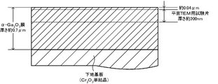
- FIG. 6 is a schematic cross-sectional view showing a cutout position of a test piece for plane TEM observation.
- An enlarged photograph of a part of FIG. 7. A photograph of a BF-STEM image near the nunchaku-shaped tissue shown in FIG. Photograph of HAADF-STEM image of rod-shaped region A.
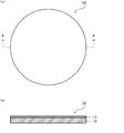
- FIG. 1A and 1B are explanatory views of the laminated structure 10, FIG. 1A is a plan view, and FIG. 1B is a cross-sectional view taken along the line AA.
- the laminated structure 10 is a plate-shaped member, and has a semiconductor film 14 on a base substrate 12.
- the plan view figure when the laminated structure 10 is viewed in a plan view is circular in the present embodiment.
- the "circular shape" does not have to be a perfect circular shape, and may be a substantially circular shape that can be generally recognized as a circular shape. For example, a part of the circle may be cut out for the purpose of specifying the crystal orientation or for other purposes.
- the plan view figure of the laminated structure 10 is not limited to a circle, and may be, for example, a polygon (a quadrangle such as a square or a rectangle, a pentagon, a hexagon, or the like).
- the base substrate 12 preferably has a layer of an oxide ( ⁇ -Cr 2 O 3 , ⁇ -Fe 2 O 3, etc.) whose lattice constant is closer to ⁇ -Ga 2 O 3 than sapphire, and ⁇ -Cr 2 Those provided with a single crystal layer of O 3 or ⁇ -Cr 2 O 3 system solid solution are more preferable.
- ⁇ -Cr 2 O 3 ⁇ -Fe 2 O 3, etc.
- the semiconductor film 14 is a semiconductor film having a corundum-type crystal structure composed of an ⁇ -Ga 2 O 3 or ⁇ -Ga 2 O 3 system solid solution, that is, an ⁇ -Ga 2 O 3 system semiconductor film.
- ⁇ -Ga 2 O 3 belongs to a trigonal crystal group and has a corundum-type crystal structure.
- the ⁇ -Ga 2 O 3 system solid solution is a solid solution of other components in ⁇ -Ga 2 O 3 , and the corundum type crystal structure is maintained. Examples of other components include Al 2 O 3 , In 2 O 3 , Cr 2 O 3 , Fe 2 O 3 , Rh 2 O 3 , V 2 O 3 , and Ti 2 O 3 .
- the nunchaku-shaped structure 20 shown in FIG. 2 is observed in a flat TEM bright-field image when an electron beam is incident parallel to the ⁇ 001> direction.
- the nunchaku-shaped structure 20 is a structure having rod-shaped areas 24, 24 wider than the fine line-shaped area 22 at both ends of the thin line-shaped area 22.
- the nunchaku-type tissue 20 appears as a dark part in a plane TEM bright-field image.
- the observation of the plane TEM bright-field image is performed as follows. That is, the sample is cut out so as to include a surface having a depth of about 0.04 ⁇ m from the surface of the semiconductor film 14 (the surface opposite to the surface on the base substrate 12 side), and the thickness of the portion of the sample that serves as the measurement field of view.
- a plurality of linear structures are observed in a cross-sectional TEM bright-field image when an electron beam is incident in parallel in the ⁇ 1-10> direction.
- the tissue observed as a linear dark part in the TEM bright-field image is generally recognized as a dislocation.
- such an indelible linear structure is not attributed to either blade dislocations or spiral dislocations.
- the planar STEM observation in which the electron beam is incident parallel to the Nunchak-shaped structure 20 observed in the planar TEM image of the semiconductor film 14 in the ⁇ 001> direction is performed, the planar STEM bright-field image is captured by the planar TEM. A dark area corresponding to the image appears.
- the Ga atomic image is magnified to a level where it can be recognized (for example, at a magnification of 4 million times or more) in the plane STEM, the increase or decrease of the atomic plane and the large deviation of the atomic arrangement do not occur in any region of the nunchaku-type structure 20. I can't confirm.
- the atomic planes increase or decrease or shift in the Ga atomic image, so the Nunchak-type structure is not only blade-shaped dislocations and spiral dislocations, but also mixed dislocations and basal plane dislocations. In addition, it is not attributed to surface defects such as stacking defects and grain boundaries.
- the plane STEM bright-field image is observed as follows.
- the sample is cut out so as to include a surface having a depth of about 0.04 ⁇ m from the surface of the semiconductor film 14 (the surface opposite to the surface on the base substrate 12 side), and the thickness of the portion of the sample that serves as the measurement field of view. Is processed by ion milling so that the value is 70 nm. Then, an electron beam is incident parallel to the measurement field of view in the ⁇ 001> direction at an acceleration voltage of 200 kV, and the STEM bright field image is observed.
- the nunchak-type structure 20 contained in the semiconductor film 14 is observed as a dark part in the plane TEM bright-field image, dislocations (blade dislocations, spiral dislocations, mixed dislocations, basal plane dislocations) and stacking defects , Not attributed to surface defects such as grain boundaries. Further, STEM-EDS analysis and electron diffraction analysis of TEM were carried out in the region where the nunchaku-type structure 20 was detected, but no heterogeneous phase or agglutination of foreign substances was observed.
- the nunchak-type structure 20 observed in the planar TEM image of the semiconductor film 14 is considered to be a crystal defect that is not attributed to blade-like dislocations, spiral dislocations, mixed dislocations, basal plane dislocations, and surface defects such as stacking defects and grain boundaries. ..
- the structure of the nunchaku-type structure 20 is unknown, but in the planar STEM image, the Ga atomic image is slightly unclear compared to the peripheral part (non-defect part), so it is considered that the Ga atomic arrangement is slightly overlooked. It is speculated that the atomic position may have been replaced by O.
- the density of the nunchaku-type structure 20 of the semiconductor film 14 is preferably as low as possible from the viewpoint of crystallinity, specifically, 1.0 ⁇ 10 10 / cm 2 or less, and 1.0 ⁇ 10 9 / cm 2 or less. Is more preferable, and 1.0 ⁇ 10 8 / cm 2 or less is further preferable.
- the density of the nunchaku-type structure 20 of the semiconductor film 14 is preferably a certain density from the viewpoint of crack suppression, specifically, 1.0 ⁇ 10 4 / cm 2 or more, and 1.0 ⁇ 10 5 / cm 2 or more is more preferable, and 1.0 ⁇ 10 6 / cm 2 or more is further preferable. Therefore, in order to achieve both crystallinity and crack suppression, the density of the nunchaku-type structure of the semiconductor film 14 is preferably 1.0 ⁇ 10 6 / cm 2 or more and 1.0 ⁇ 10 8 / cm 2 or less.
- the total length of the nunchaku-shaped structure 20 of the semiconductor film 14, that is, the length of the line segment connecting the outer ends of the rod-shaped regions 24 and 24 is not particularly limited, but is typically 100 to 800 nm.
- the length of the thin linear region 22 is not particularly limited, but is typically 50 to 500 nm.
- the length of the rod-shaped region 24 is not particularly limited, but is typically 20 to 150 nm.
- the nunchaku-shaped structure 20 of the semiconductor film 14 may have a part of the thin linear region 22 bent (see FIG. 3A) or may be substantially linear (see FIG. 3B). .. In terms of numbers, the former tends to be larger than the latter. It is considered that the former is more effective in dispersing the stress in the semiconductor film 14, and is therefore preferable in terms of suppressing cracks and warpage of the semiconductor film.
- the nunchaku-shaped structure 20 of the semiconductor film 14 may have the two rod-shaped regions 24 and 24 substantially parallel in the longitudinal direction (see FIG. 3C) or may have an angle (FIG. 3). (D), (e)).
- the former tends to be larger than the latter. It is considered that the former is more effective in dispersing the stress in the semiconductor film 14, and is therefore preferable in terms of suppressing cracks and warpage of the semiconductor film.
- the area of the film surface of the semiconductor film 14 substantially coincides with the area of the underlying substrate 12.
- the area of the film surface of the semiconductor film 14 is preferably 20 cm 2 or more, more preferably 70 cm 2 or more, and further preferably 170 cm 2 or more. By increasing the area of the semiconductor film 14 in this way, it is possible to obtain a large number of semiconductor elements from one semiconductor film 14, and it is possible to reduce the manufacturing cost.
- the upper limit of the size of the semiconductor film 14 is not particularly limited, but is typically 700 cm 2 or less on one side.
- the average film thickness of the semiconductor film 14 is preferably 3 ⁇ m or more, more preferably 5 ⁇ m or more, still more preferably 8 ⁇ m or more.
- the semiconductor film 14 can contain a Group 14 element as a dopant at a ratio of 1.0 ⁇ 10 16 to 1.0 ⁇ 10 21 / cm 3.
- the Group 14 elements are the Group 14 elements according to the periodic table formulated by the IUPAC (International Union of Pure and Applied Chemistry). Specifically, carbon (C), silicon (Si), germanium (Ge), and so on. It is either tin (Sn) or lead (Pb).
- the amount of the dopant can be appropriately changed according to the desired characteristics, but is preferably 1.0 ⁇ 10 16 to 1.0 ⁇ 10 21 / cm 3 , and more preferably 1.0 ⁇ 10 17 to 1.0. ⁇ 10 19 / cm 3 . It is preferable that these dopants are uniformly distributed in the film, and the dopant concentrations on the front surface and the back surface of the semiconductor film 14 are about the same.
- the semiconductor film 14 is preferably an alignment film oriented in a specific plane orientation.
- the orientation of the semiconductor film 14 can be examined by a known method, and can be examined, for example, by performing reverse pole map orientation mapping using an electron backscatter diffraction device (EBSD).
- EBSD electron backscatter diffraction device
- the semiconductor film may be c-axis oriented, or may be c-axis oriented and also oriented in the in-plane direction.
- the method for producing the semiconductor film 14 includes (a) a step of obtaining the laminated structure 10 and (b) a step of peeling the semiconductor film 14 from the base substrate 12.
- the laminated structure 10 has an oxide ( ⁇ -Cr 2 O 3 , ⁇ -Fe 2 O 3 , ⁇ -Cr ) whose lattice constant is closer to ⁇ -Ga 2 O 3 than that of sapphire.
- the base substrate 12 such as 2 O 3 solid solution
- the base substrate 12 include a Cr 2 O 3 single crystal substrate.
- the film forming method is not particularly limited, and a known method can be adopted. As the film forming method, mist CVD, HVPE, MBE, MOCVD, sputtering, and hydrothermal method are preferable, mist CVD and HVPE are more preferable, and mist CVD is further preferable.
- FIG. 4 is a schematic cross-sectional view showing the configuration of the mist CVD apparatus 40.
- the mist CVD apparatus 40 includes a susceptor 50 on which the base substrate 12 is placed, a dilution gas source 42a, a carrier gas source 42b, and a flow rate control valve 43a for adjusting the flow rate of the dilution gas sent out from the dilution gas source 42a.
- the flow control valve 43b for adjusting the flow rate of the carrier gas sent out from the carrier gas source 42b, the mist generation source 44 containing the raw material solution 44a, the container 45 containing the water 45a, and the bottom surface of the container 45.
- the quartz tube 47 serving as a film forming chamber
- a heater 48 installed around the quartz tube 47
- an exhaust port 51 The susceptor 50 is made of quartz, and the surface on which the base substrate 12 is placed is inclined from the horizontal plane.
- the raw material solution 44a used in the mist CVD method is not limited as long as it is a solution that can obtain an ⁇ -Ga 2 O 3 system semiconductor film, and is, for example, an organic metal complex of Ga, a halide of Ga, and a halide of Ga.
- examples thereof include those in which one or more of organic metal complexes of Ga and a metal forming a solid solution are dissolved in a solvent.
- organometallic complexes include acetylacetonate complexes
- examples of halides include GaCl 3 and GaBr 3 .
- the halide may be directly dissolved in the solvent or hydrogen halide in water.
- the halide may be dissolved in a solution to which an acid (for example, hydrochloric acid) is added, or metal Ga may be dissolved in a solution of water and a hydrohalic acid.
- an acid for example, hydrochloric acid
- metal Ga may be dissolved in a solution of water and a hydrohalic acid.
- a solution containing these components may be added to the raw material solution.
- an additive such as hydrohalic acid may be added to the raw material solution. Water, alcohol, or the like can be used as the solvent.
- the obtained raw material solution 44a is atomized to generate mist 44b.
- a preferred example of the atomization method is a method of vibrating the raw material solution 44a using the ultrasonic vibrator 46.
- the obtained mist 44b is conveyed to the film forming chamber using a carrier gas.
- the carrier gas is not particularly limited, but one or more kinds of an inert gas such as oxygen, ozone and nitrogen, and a reducing gas such as hydrogen can be used.
- the film forming chamber (quartz tube 47) is provided with a base substrate 12.
- the mist 44b conveyed to the film forming chamber is thermally decomposed and chemically reacted there to form a film on the substrate 12.
- the reaction temperature varies depending on the type of the raw material solution, but is preferably 300 to 800 ° C, more preferably 350 to 700 ° C.
- the atmosphere in the film forming chamber is not particularly limited as long as a desired semiconductor film can be obtained, and may be an oxygen gas atmosphere, an inert gas atmosphere, a vacuum or a reducing atmosphere, but an air atmosphere is preferable.
- a droplet of the raw material solution 44a may be used in place of or in addition to the mist 44b.
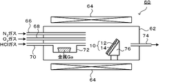
- FIG. 5 is a schematic cross-sectional view showing the configuration of the vapor deposition apparatus 60 using HVPE.
- the vapor phase growth apparatus 60 includes a reaction vessel 62 and a heater 64.
- the reaction vessel 62 is a vessel made of a material (for example, quartz) that does not react with various raw materials and products.
- a carrier gas supply pipe 66, an oxidation gas supply pipe 68, and a raw material supply pipe 70 are attached to one side surface of the pair of side surfaces of the reaction vessel 62 facing each other, and an exhaust pipe 74 is attached to the other side surface.
- the carrier gas supply pipe 66 supplies a carrier gas (for example, nitrogen, a rare gas, etc.) into the reaction vessel 62.
- the oxidation gas supply pipe 68 supplies oxygen gas as an oxidation gas into the reaction vessel 62. In addition to oxygen, water vapor, nitrous oxide, or the like may be supplied as the oxidation gas.
- halogen gas for example, chlorine gas
- hydrogen halide gas for example, hydrogen chloride gas
- the raw material supply pipe 70 supplies gallium halide gas as a raw material gas into the reaction vessel 62.
- the halogen gas or the hydrogen halide gas may be supplied together with a carrier gas such as nitrogen or a rare gas.
- a susceptor 76 for detachably holding the base substrate 12 is provided downstream of the supply pipes 66, 68, 70 in the reaction vessel 62.
- the exhaust pipe 74 discharges the unreacted gas in the reaction vessel 62.
- a vacuum pump may be connected to the exhaust pipe 74, and the degree of vacuum in the reaction vessel 62 may be adjusted by the vacuum pump. Thereby, the gas phase reaction can be suppressed and the growth rate distribution can be improved.
- the heater 64 is arranged so as to surround the reaction vessel 62.
- As the heater 64 for example, a resistance heating type heater or the like can be adopted.
- the oxygen gas supplied from the oxidation gas supply pipe 68 and the raw material gas (gallium halide gas) supplied from the raw material supply pipe 70 react with each other to form a semiconductor film 14 (gallium halide gas) on the base substrate 12.
- ⁇ -Ga 2 O 3 film is formed.
- the film formation temperature is not particularly limited, and may be appropriately set in the range of, for example, 300 ° C. or higher and 800 ° C. or lower.
- the partial pressure of the oxygen gas or the raw material gas is not particularly limited.
- the partial pressure of the raw material gas may be in the range of 0.05 kPa or more and 10 kPa or less, and the partial pressure of the oxygen gas is 0.25 kPa or more and 50 kPa or less. It may be a range.
- the growth time may be appropriately set according to the design value of the film thickness of the semiconductor film 14. As a result, the laminated structure 10 is obtained.
- Step of peeling the semiconductor film 14 from the base substrate 12 The method of peeling the semiconductor film 14 from the base substrate 12 of the laminated structure 10 at room temperature obtained as described above from the base substrate 12 is particularly limited. A known method can be used instead of the one. Examples of the peeling method include a method of peeling by applying a mechanical impact, a method of peeling by applying heat and utilizing thermal stress, and a method of peeling by applying vibration such as ultrasonic waves. By peeling, the semiconductor film 14 can be obtained as a self-supporting film. Alternatively, the semiconductor film 14 can be reprinted on another support substrate.
- the ⁇ -Ga 2 O 3 system semiconductor film of the present embodiment described above is a nunchaku having rod-shaped regions at both ends of a thin linear region in a flat TEM bright-field image when an electron beam is incident in parallel in the ⁇ 001> direction. Type tissue is observed. Therefore, it is possible to suppress the occurrence of cracks in the ⁇ -Ga 2 O 3 system semiconductor film.
- Example 1 The ⁇ -Ga 2 O 3 film (semiconductor film) was formed by the following method using the mist CVD apparatus 40 shown in FIG.
- the base substrate 12 a commercially available Cr 2 O 3 single crystal (8 mm ⁇ 8 mm, thickness 0.5 mm, c-plane, no off-angle, hereinafter referred to as Cr 2 O 3 substrate) was used.
- the obtained raw material solution 44a was housed in the mist generation source 44 of the mist CVD apparatus 40 of FIG.
- the Cr 2 O 3 substrate was placed on the susceptor 50 as the base substrate 12, and the heater 48 was operated to raise the temperature inside the quartz tube 47 to 570 ° C.
- the flow control valves 43a and 43b are opened to supply the diluted gas and the carrier gas into the quartz tube 47 from the diluted gas source 42a and the carrier gas source 42b, and the atmosphere of the quartz tube 47 is sufficiently filled with the diluted gas and the carrier gas.
- the flow rate of the diluting gas was adjusted to 0.5 L / min
- the flow rate of the carrier gas was adjusted to 1 L / min. Nitrogen gas was used as the diluting gas and the carrier gas.
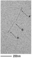
- FIGS. 7 and 8 show a two-field planar TEM observation bright-field images.
- FIG. 9 shows a bright field image in which a part of FIG. 7 is enlarged.
- a nunchaku-type structure was observed in the bright-field image of the plane TEM observation.
- the nunchaku-type structure had rod-shaped regions A and A'at both ends of the fine linear region B.
- nunchaku-type tissues were observed at 7 sites.
- the density of the nunchaku-type tissue was calculated from the area of the measurement field of view and the number of nunchaku-type tissues, it was 3.4 ⁇ 10 7 / cm 2 .
- the observed nunchak-shaped structure had a total length (the length of the line segment connecting the points of the outer ends of the rod-shaped region) of 376 to 645 nm, a rod-shaped region of 82 nm to 131 nm (average 107 nm), and a fine linear region.
- the length (the length of the line segment connecting both ends of the thin linear region) was 245 nm to 408 nm (average 352 nm).
- FIG. 10 The BF-STEM image near the nunchaku-type tissue shown in FIG. 9 is shown in FIG.
- FIG. 10 a nunchaku-shaped structure having rod-shaped regions A and A'at both ends of the thin line-shaped region B was observed.
- the HAADF-STEM images obtained by enlarging the rod-shaped region A and the thin line-shaped region B are shown in FIGS. 11 and 12, respectively.
- the vicinity of the arrow in FIG. 11 corresponds to the rod-shaped region A
- the vicinity of the arrow in FIG. 12 corresponds to the thin line region B.
- the white dots in the figure indicate the cation atom image (Ga atom).
- Example 1 As the base substrate 12, an ⁇ -Ga 2 O 3 film was formed in the same manner as in Example 1 except that a sapphire substrate having a diameter of 5.08 cm (2 inches), a thickness of 0.65 mm, a c-plane, and no off-angle was used. It was formed and various evaluations were carried out. As a result of performing EDS measurement on the film surface on the film formation side of the obtained film, only Ga and O were detected, and it was found that the obtained film was a Ga oxide.
- the Ga oxide film has a corundum-type crystal structure in which the Ga oxide film is oriented in the c-axis direction in the normal direction of the substrate and is also oriented in the plane. From these, it was shown that an alignment film composed of ⁇ -Ga 2 O 3 was formed.
- the plane TEM observation of the surface on the film-forming side was carried out, no nunchaku-type structure was observed from the bright-field image.
- the appearance of the obtained semiconductor film was observed using an industrial microscope, many cracks were observed.
- the present invention can be used, for example, as a material for power semiconductors.
Abstract
This α-Ga2O3 semiconductor film has a nunchuck structure 20 which is observed in a planar TEM bright-field image taken with an electron beam incident in parallel with the <001> direction, and has, at both ends of a thin line-like region 22, rod-like regions 24, 24 wider than the thin line-like region 22.
Description
本発明は、α-Ga2O3系半導体膜に関する。
The present invention relates to an α-Ga 2 O 3 system semiconductor film.
近年、酸化ガリウム(Ga2O3)が半導体用材料として着目されている。酸化ガリウムはα、β、γ、δ及びεの5つの結晶形を有することが知られているが、この中で、α-Ga2O3はバンドギャップが5.3eVと非常に大きく、パワー半導体用材料として期待を集めている。しかしながら、α-Ga2O3は順安定相であるため、単結晶基板が実用化されておらず、サファイア基板へのヘテロエピタキシャル成長で形成されるのが一般的である。
In recent years, gallium oxide (Ga 2 O 3 ) has been attracting attention as a material for semiconductors. Gallium oxide is known to have five crystal forms of α, β, γ, δ and ε. Among them, α-Ga 2 O 3 has a very large bandgap of 5.3 eV and power. It is expected as a material for semiconductors. However, since α-Ga 2 O 3 has a forward stable phase, a single crystal substrate has not been put into practical use, and it is generally formed by heteroepitaxial growth on a sapphire substrate.
例えば、特許文献1には、コランダム型結晶構造を有する下地基板と、コランダム型結晶構造を有する半導体層と、コランダム型結晶構造を有する絶縁膜とを備えた半導体装置が開示されており、サファイア基板上に、半導体層としてα-Ga2O3膜を成膜した例が記載されている。また、特許文献2には、コランダム構造を有する結晶性酸化物半導体を主成分として含むn型半導体層と、六方晶の結晶構造を有する無機化合物を主成分とするp型半導体層と、電極とを備えた半導体装置が開示されている。この特許文献2の実施例には、c面サファイア基板上に、n型半導体層として準安定相であるコランダム構造を有するα-Ga2O3膜を、p型半導体層として六方晶の結晶構造を有するα-Rh2O3膜を形成して、ダイオードを作製することが開示されている。
For example, Patent Document 1 discloses a semiconductor device including a base substrate having a corundum-type crystal structure, a semiconductor layer having a corundum-type crystal structure, and an insulating film having a corundum-type crystal structure, and a sapphire substrate. An example in which an α-Ga 2 O 3 film is formed as a semiconductor layer is described above. Further, Patent Document 2 describes an n-type semiconductor layer containing a crystalline oxide semiconductor having a corundum structure as a main component, a p-type semiconductor layer containing an inorganic compound having a hexagonal crystal structure as a main component, and an electrode. A semiconductor device comprising the above is disclosed. In the embodiment of Patent Document 2, an α-Ga 2 O 3 film having a corundum structure which is a semi-stable phase as an n-type semiconductor layer is formed on a c-plane sapphire substrate, and a hexagonal crystal structure is used as a p-type semiconductor layer. It is disclosed that a diode is produced by forming an α-Rh 2 O 3 film having.
ところで、異種基板上にα-Ga2O3膜を結晶成長させる際に、クラックや結晶欠陥が生じるという問題がある。α-Ga2O3と異種コランダム材料との混晶であるInAlGaO系の半導体膜を成膜する際も、通常、異種基板上に結晶成長を行うため、エピタキシャル膜にクラックが入る等の問題が生じている。この問題に対処する技術として、特許文献3では、クラックの少ないα-Ga2O3膜を作製することが開示されている。また、特許文献4には、エピタキシャル膜の成膜時にボイドを含ませることにより、クラックが低減されたα-Ga2O3膜を作製することが開示されている。
By the way, there is a problem that cracks and crystal defects occur when the α-Ga 2 O 3 film is crystal-grown on a dissimilar substrate. When forming an InAlGaO-based semiconductor film, which is a mixed crystal of α-Ga 2 O 3 and a dissimilar corundum material, crystals usually grow on the dissimilar substrate, which causes problems such as cracks in the epitaxial film. It is happening. As a technique for dealing with this problem, Patent Document 3 discloses that an α-Ga 2 O 3 film having few cracks is produced. Further, Patent Document 4 discloses that an α-Ga 2 O 3 film having reduced cracks is produced by including voids when the epitaxial film is formed.
このように種々のα-Ga2O3膜が作製されているものの、これまでとは異なる有用なα-Ga2O3系半導体膜の開発が望まれていた。
Although various α-Ga 2 O 3 films have been produced in this way, it has been desired to develop a useful α-Ga 2 O 3 system semiconductor film different from the conventional ones.
本発明はこのような課題を解決するためになされたものであり、新規なα-Ga2O3系半導体膜を提供することを主目的とする。
The present invention has been made to solve such a problem, and an object of the present invention is to provide a novel α-Ga 2 O 3 system semiconductor film.
本発明のα-Ga2O3系半導体膜は、<001>方向に平行に電子線を入射させたときの平面TEM明視野像において、細線状領域の両端に前記細線状領域よりも幅の広い棒状領域を有するヌンチャク(nunchaku)型組織が観察されるものである。
The α-Ga 2 O 3 system semiconductor film of the present invention has a width wider than that of the fine line region at both ends of the fine line region in a plane TEM bright-field image when an electron beam is incident in parallel in the <001> direction. A nunchaku-type tissue with a large rod-like region is observed.
このα-Ga2O3系半導体膜は、これまでに知られていない新規なものであり、クラックの発生が抑制される。
This α-Ga 2 O 3 system semiconductor film is a novel one that has not been known so far, and the occurrence of cracks is suppressed.
[積層構造体]
図1は、積層構造体10の説明図であり、(a)は平面図、(b)はA-A断面図である。 [Laminated structure]
1A and 1B are explanatory views of the laminatedstructure 10, FIG. 1A is a plan view, and FIG. 1B is a cross-sectional view taken along the line AA.
図1は、積層構造体10の説明図であり、(a)は平面図、(b)はA-A断面図である。 [Laminated structure]
1A and 1B are explanatory views of the laminated
積層構造体10は、板状の部材であり、下地基板12上に半導体膜14を備えたものである。この積層構造体10を平面視したときの平面視図形は、本実施形態では円形である。「円形」とは、完全な円形状である必要はなく、全体として概ね円形と認識されうる略円形状であってもよい。例えば、円形の一部が結晶方位の特定又はその他の目的のために切り欠かれた形状であってもよい。また、積層構造体10の平面視図形は円形に限定されるものではなく、例えば多角形(正方形や長方形などの四角形のほか、五角形や六角形など)であってもよい。
The laminated structure 10 is a plate-shaped member, and has a semiconductor film 14 on a base substrate 12. The plan view figure when the laminated structure 10 is viewed in a plan view is circular in the present embodiment. The "circular shape" does not have to be a perfect circular shape, and may be a substantially circular shape that can be generally recognized as a circular shape. For example, a part of the circle may be cut out for the purpose of specifying the crystal orientation or for other purposes. Further, the plan view figure of the laminated structure 10 is not limited to a circle, and may be, for example, a polygon (a quadrangle such as a square or a rectangle, a pentagon, a hexagon, or the like).
下地基板12は、格子定数がサファイアよりもα-Ga2O3に近い酸化物(α-Cr2O3やα-Fe2O3など)の層を備えたものが好ましく、α-Cr2O3又はα-Cr2O3系固溶体の単結晶層を備えたものがより好ましい。
The base substrate 12 preferably has a layer of an oxide (α-Cr 2 O 3 , α-Fe 2 O 3, etc.) whose lattice constant is closer to α-Ga 2 O 3 than sapphire, and α-Cr 2 Those provided with a single crystal layer of O 3 or α-Cr 2 O 3 system solid solution are more preferable.
半導体膜14は、α-Ga2O3又はα-Ga2O3系固溶体からなるコランダム型結晶構造を有するもの、すなわちα-Ga2O3系半導体膜である。α-Ga2O3は、三方晶系の結晶群に属し、コランダム型結晶構造をとる。また、α-Ga2O3系固溶体は、α-Ga2O3に他の成分が固溶したものであり、コランダム型結晶構造が維持されている。他の成分としては、例えば、Al2O3、In2O3、Cr2O3、Fe2O3、Rh2O3、V2O3、Ti2O3などが挙げられる。
The semiconductor film 14 is a semiconductor film having a corundum-type crystal structure composed of an α-Ga 2 O 3 or α-Ga 2 O 3 system solid solution, that is, an α-Ga 2 O 3 system semiconductor film. α-Ga 2 O 3 belongs to a trigonal crystal group and has a corundum-type crystal structure. Further, the α-Ga 2 O 3 system solid solution is a solid solution of other components in α-Ga 2 O 3 , and the corundum type crystal structure is maintained. Examples of other components include Al 2 O 3 , In 2 O 3 , Cr 2 O 3 , Fe 2 O 3 , Rh 2 O 3 , V 2 O 3 , and Ti 2 O 3 .
半導体膜14は、<001>方向に平行に電子線を入射させたときの平面TEM明視野像において、図2に示すヌンチャク型組織20が観察される。ヌンチャク型組織20は、細線状領域22の両端にその細線状領域22よりも幅の広い棒状領域24,24を有する組織である。ヌンチャク型組織20は、平面TEM明視野像において暗部として現れる。平面TEM明視野像の観察は、次のようにして行う。すなわち、半導体膜14の表面(下地基板12側の面とは反対側の面)からの深さが約0.04μmの面を含むように試料を切り出し、試料のうち測定視野となる部分の厚みが200nmとなるようにイオンミリングによって加工する。そして、測定視野となる部分に対し、加速電圧300kVで<001>方向に平行に電子線を入射させてTEM明視野像を観察する。
In the semiconductor film 14, the nunchaku-shaped structure 20 shown in FIG. 2 is observed in a flat TEM bright-field image when an electron beam is incident parallel to the <001> direction. The nunchaku-shaped structure 20 is a structure having rod- shaped areas 24, 24 wider than the fine line-shaped area 22 at both ends of the thin line-shaped area 22. The nunchaku-type tissue 20 appears as a dark part in a plane TEM bright-field image. The observation of the plane TEM bright-field image is performed as follows. That is, the sample is cut out so as to include a surface having a depth of about 0.04 μm from the surface of the semiconductor film 14 (the surface opposite to the surface on the base substrate 12 side), and the thickness of the portion of the sample that serves as the measurement field of view. Is processed by ion milling so that the value is 200 nm. Then, an electron beam is incident on the portion to be the measurement field of view in parallel with the <001> direction at an acceleration voltage of 300 kV, and the TEM bright field image is observed.
半導体膜14は、<1-10>方向に平行に電子線を入射させたときの断面TEM明視野像において、複数の線状組織が観察される。この明視野像で観察された線状組織の中には、同じ断面TEMの暗視野像g*=110及び暗視野像g*=00-6のいずれにおいても消えない組織が存在する。TEM明視野像で線状の暗部として観察される組織は一般的には転位と認識される。刃状転位、らせん転位は断面TEMの暗視野像g*=110及び暗視野像g*=00-6を観察し、消失するかどうかで刃状転位、らせん転位の帰属を決定することができるが、こうした消えない線状組織は、刃状転位にもらせん転位にも帰属されない。また、半導体膜14の平面TEM像で観察されたヌンチャク型組織20に対し、<001>方向に平行に電子線を入射させた平面STEM観察を実施しても、平面STEM明視野像に平面TEM像と対応する暗部が現れる。平面STEMにおいて、Ga原子像が認められるレベルまで拡大(例えば倍率400万倍以上)して観察しても、ヌンチャク型組織20のいずれの領域においても、原子面の増減や原子配列の大きなずれは確認できない。転位や面欠陥(積層欠陥、粒界など)では、Ga原子像において原子面の増減やずれが認められるため、ヌンチャク型組織は刃状転位、らせん転位だけでなく、混合転位、基底面転位、並びに積層欠陥、粒界等の面欠陥にも帰属されない。なお、平面STEM明視野像の観察は、次のようにして行う。すなわち、半導体膜14の表面(下地基板12側の面とは反対側の面)からの深さが約0.04μmの面を含むように試料を切り出し、試料のうち測定視野となる部分の厚みが70nmとなるようにイオンミリングによって加工する。そして、測定視野となる部分に対し、加速電圧200kVで<001>方向に平行に電子線を入射させてSTEM明視野像を観察する。以上から、半導体膜14に含まれるヌンチャク型組織20は平面TEM明視野像において暗部として観察されるにも関わらず、転位(刃状転位、らせん転位、混合転位、基底面転位)や、積層欠陥、粒界等の面欠陥に帰属されない。また、ヌンチャク型組織20が検出される領域でSTEM-EDS分析やTEMの電子線回折分析を実施したが、異相や異物の凝集等は認められない。したがって、半導体膜14の平面TEM像で認められるヌンチャク型組織20は、刃状転位、らせん転位、混合転位、基底面転位、及び積層欠陥、粒界等の面欠陥に帰属されない結晶欠陥とも考えられる。ヌンチャク型組織20の構造は不明だが、平面STEM像ではGa原子像が周辺部(非欠陥部)と比較してわずかに不鮮明なことから、Ga原子配列が若干みだれた状態とも考えられ、Gaの原子位置がOと置き換わっている可能性を推測している。
In the semiconductor film 14, a plurality of linear structures are observed in a cross-sectional TEM bright-field image when an electron beam is incident in parallel in the <1-10> direction. Among the linear structures observed in this bright-field image, there is a structure that does not disappear in either the dark-field image g * = 110 or the dark-field image g * = 00-6 of the same cross-sectional TEM. The tissue observed as a linear dark part in the TEM bright-field image is generally recognized as a dislocation. For blade-shaped dislocations and spiral dislocations, the dark-field image g * = 110 and dark-field image g * = 00-6 of the cross-sectional TEM can be observed, and the attribution of blade-shaped dislocations and spiral dislocations can be determined by whether or not they disappear. However, such an indelible linear structure is not attributed to either blade dislocations or spiral dislocations. Further, even if the planar STEM observation in which the electron beam is incident parallel to the Nunchak-shaped structure 20 observed in the planar TEM image of the semiconductor film 14 in the <001> direction is performed, the planar STEM bright-field image is captured by the planar TEM. A dark area corresponding to the image appears. Even if the Ga atomic image is magnified to a level where it can be recognized (for example, at a magnification of 4 million times or more) in the plane STEM, the increase or decrease of the atomic plane and the large deviation of the atomic arrangement do not occur in any region of the nunchaku-type structure 20. I can't confirm. In the case of dislocations and surface defects (stacking defects, grain boundaries, etc.), the atomic planes increase or decrease or shift in the Ga atomic image, so the Nunchak-type structure is not only blade-shaped dislocations and spiral dislocations, but also mixed dislocations and basal plane dislocations. In addition, it is not attributed to surface defects such as stacking defects and grain boundaries. The plane STEM bright-field image is observed as follows. That is, the sample is cut out so as to include a surface having a depth of about 0.04 μm from the surface of the semiconductor film 14 (the surface opposite to the surface on the base substrate 12 side), and the thickness of the portion of the sample that serves as the measurement field of view. Is processed by ion milling so that the value is 70 nm. Then, an electron beam is incident parallel to the measurement field of view in the <001> direction at an acceleration voltage of 200 kV, and the STEM bright field image is observed. From the above, although the nunchak-type structure 20 contained in the semiconductor film 14 is observed as a dark part in the plane TEM bright-field image, dislocations (blade dislocations, spiral dislocations, mixed dislocations, basal plane dislocations) and stacking defects , Not attributed to surface defects such as grain boundaries. Further, STEM-EDS analysis and electron diffraction analysis of TEM were carried out in the region where the nunchaku-type structure 20 was detected, but no heterogeneous phase or agglutination of foreign substances was observed. Therefore, the nunchak-type structure 20 observed in the planar TEM image of the semiconductor film 14 is considered to be a crystal defect that is not attributed to blade-like dislocations, spiral dislocations, mixed dislocations, basal plane dislocations, and surface defects such as stacking defects and grain boundaries. .. The structure of the nunchaku-type structure 20 is unknown, but in the planar STEM image, the Ga atomic image is slightly unclear compared to the peripheral part (non-defect part), so it is considered that the Ga atomic arrangement is slightly overlooked. It is speculated that the atomic position may have been replaced by O.
半導体膜14のヌンチャク型組織20の密度は、結晶性の観点では少ない方が好ましく、具体的には、1.0×10¹⁰/cm2以下が好ましく、1.0×109/cm2以下がより好ましく、1.0×108/cm2以下が更に好ましい。一方、半導体膜14のヌンチャク型組織20の密度は、クラック抑制の観点ではある程度の密度であることが好ましく、具体的には、1.0×104/cm2以上が好ましく、1.0×105/cm2以上がより好ましく、1.0×106/cm2以上が更に好ましい。そのため、結晶性とクラック抑制とを両立するには、半導体膜14のヌンチャク型組織の密度が1.0×106/cm2以上1.0×108/cm2以下であることが好ましい。
The density of the nunchaku-type structure 20 of the semiconductor film 14 is preferably as low as possible from the viewpoint of crystallinity, specifically, 1.0 × 10 10 / cm 2 or less, and 1.0 × 10 9 / cm 2 or less. Is more preferable, and 1.0 × 10 8 / cm 2 or less is further preferable. On the other hand, the density of the nunchaku-type structure 20 of the semiconductor film 14 is preferably a certain density from the viewpoint of crack suppression, specifically, 1.0 × 10 4 / cm 2 or more, and 1.0 × 10 5 / cm 2 or more is more preferable, and 1.0 × 10 6 / cm 2 or more is further preferable. Therefore, in order to achieve both crystallinity and crack suppression, the density of the nunchaku-type structure of the semiconductor film 14 is preferably 1.0 × 10 6 / cm 2 or more and 1.0 × 10 8 / cm 2 or less.
半導体膜14のヌンチャク型組織20の全長、すなわち棒状領域24,24の外端同士を結んだ線分の長さは、特に限定するものではないが、典型的には100~800nmである。細線状領域22の長さは、特に限定するものではないが、典型的には50~500nmである。棒状領域24の長さは、特に限定するものではないが、典型的には20~150nmである。
The total length of the nunchaku-shaped structure 20 of the semiconductor film 14, that is, the length of the line segment connecting the outer ends of the rod-shaped regions 24 and 24 is not particularly limited, but is typically 100 to 800 nm. The length of the thin linear region 22 is not particularly limited, but is typically 50 to 500 nm. The length of the rod-shaped region 24 is not particularly limited, but is typically 20 to 150 nm.
半導体膜14のヌンチャク型組織20は、細線状領域22の一部が屈曲していてもよいし(図3(a)参照)、略直線状であってもよい(図3(b)参照)。数としては前者が後者よりも多い傾向にある。前者が多い方が、半導体膜14内の応力を分散する効果があると考えられるため、半導体膜のクラックや反りを抑制する点で好ましい。
The nunchaku-shaped structure 20 of the semiconductor film 14 may have a part of the thin linear region 22 bent (see FIG. 3A) or may be substantially linear (see FIG. 3B). .. In terms of numbers, the former tends to be larger than the latter. It is considered that the former is more effective in dispersing the stress in the semiconductor film 14, and is therefore preferable in terms of suppressing cracks and warpage of the semiconductor film.
半導体膜14のヌンチャク型組織20は、2つの棒状領域24,24の長手方向が略平行になっていてもよいし(図3(c)参照)、角度を有していてもよい(図3(d),(e)参照)。数としては前者が後者よりも多い傾向にある。前者が多い方が、半導体膜14内の応力を分散する効果があると考えられるため、半導体膜のクラックや反りを抑制する点で好ましい。
The nunchaku-shaped structure 20 of the semiconductor film 14 may have the two rod-shaped regions 24 and 24 substantially parallel in the longitudinal direction (see FIG. 3C) or may have an angle (FIG. 3). (D), (e)). In terms of numbers, the former tends to be larger than the latter. It is considered that the former is more effective in dispersing the stress in the semiconductor film 14, and is therefore preferable in terms of suppressing cracks and warpage of the semiconductor film.
半導体膜14の膜表面の面積は、下地基板12の面積と実質的に一致している。半導体膜14の膜表面の面積は、好ましくは20cm2以上、より好ましくは70cm2以上、さらに好ましくは170cm2以上である。このように半導体膜14を大面積化することにより、一枚の半導体膜14から半導体素子を多数個取りすることが可能となり、製造コストの低減化を図ることができる。半導体膜14の大きさの上限は特に限定されるものではないが、典型的には、片面700cm2以下である。半導体膜14の平均膜厚は、好ましくは3μm以上、より好ましくは5μm以上、さらに好ましくは8μm以上である。
The area of the film surface of the semiconductor film 14 substantially coincides with the area of the underlying substrate 12. The area of the film surface of the semiconductor film 14 is preferably 20 cm 2 or more, more preferably 70 cm 2 or more, and further preferably 170 cm 2 or more. By increasing the area of the semiconductor film 14 in this way, it is possible to obtain a large number of semiconductor elements from one semiconductor film 14, and it is possible to reduce the manufacturing cost. The upper limit of the size of the semiconductor film 14 is not particularly limited, but is typically 700 cm 2 or less on one side. The average film thickness of the semiconductor film 14 is preferably 3 μm or more, more preferably 5 μm or more, still more preferably 8 μm or more.
半導体膜14は、ドーパントとして14族元素を1.0×10¹⁶~1.0×10²¹/cm3の割合で含むことができる。ここで、14族元素はIUPAC(国際純正・応用化学連合)が策定した周期表による14族元素のことであり、具体的には、炭素(C)、珪素(Si)、ゲルマニウム(Ge)、錫(Sn)及び鉛(Pb)のいずれかの元素である。ドーパント量は所望の特性に合わせて適宜変更することができるが、好ましくは、1.0×1016~1.0×1021/cm3、より好ましくは1.0×1017~1.0×1019/cm3である。これらのドーパントは膜中に均一に分布し、半導体膜14の表面と裏面のドーパント濃度は同程度であることが好ましい。
The semiconductor film 14 can contain a Group 14 element as a dopant at a ratio of 1.0 × 10 16 to 1.0 × 10 21 / cm 3. Here, the Group 14 elements are the Group 14 elements according to the periodic table formulated by the IUPAC (International Union of Pure and Applied Chemistry). Specifically, carbon (C), silicon (Si), germanium (Ge), and so on. It is either tin (Sn) or lead (Pb). The amount of the dopant can be appropriately changed according to the desired characteristics, but is preferably 1.0 × 10 16 to 1.0 × 10 21 / cm 3 , and more preferably 1.0 × 10 17 to 1.0. × 10 19 / cm 3 . It is preferable that these dopants are uniformly distributed in the film, and the dopant concentrations on the front surface and the back surface of the semiconductor film 14 are about the same.
さらに、半導体膜14は、特定の面方位に配向した配向膜であるのが好ましい。半導体膜14の配向性は公知の方法で調べることができるが、例えば、電子線後方散乱回折装置(EBSD)を用いて、逆極点図方位マッピングを行うことで、調べることができる。例えば、半導体膜は、c軸配向していてもよいし、c軸配向すると共に面内方向にも配向していてもよい。
Further, the semiconductor film 14 is preferably an alignment film oriented in a specific plane orientation. The orientation of the semiconductor film 14 can be examined by a known method, and can be examined, for example, by performing reverse pole map orientation mapping using an electron backscatter diffraction device (EBSD). For example, the semiconductor film may be c-axis oriented, or may be c-axis oriented and also oriented in the in-plane direction.
[半導体膜の製法]
半導体膜14の製法には、(a)積層構造体10を得る工程と、(b)半導体膜14を下地基板12から剥離する工程とが含まれる。 [Manufacturing method of semiconductor film]
The method for producing thesemiconductor film 14 includes (a) a step of obtaining the laminated structure 10 and (b) a step of peeling the semiconductor film 14 from the base substrate 12.
半導体膜14の製法には、(a)積層構造体10を得る工程と、(b)半導体膜14を下地基板12から剥離する工程とが含まれる。 [Manufacturing method of semiconductor film]
The method for producing the
(a)積層構造体10を得る工程
積層構造体10は、格子定数がサファイアよりもα-Ga2O3に近い酸化物(α-Cr2O3やα-Fe2O3、α-Cr2O3系固溶体など)の下地基板12上に、半導体膜14を成膜することにより得られる。下地基板12としては、例えばCr2O3単結晶基板が挙げられる。成膜方法は、特に限定されるものではなく、公知の手法が採用可能である。成膜方法としては、ミストCVD、HVPE、MBE、MOCVD、スパッタリング、水熱法が好ましく、ミストCVD、HVPEがより好ましく、ミストCVDが更に好ましい。 (A) Step of obtaining thelaminated structure 10 The laminated structure 10 has an oxide (α-Cr 2 O 3 , α-Fe 2 O 3 , α-Cr ) whose lattice constant is closer to α-Ga 2 O 3 than that of sapphire. the base substrate 12, such as 2 O 3 solid solution), is obtained by forming a semiconductor film 14. Examples of the base substrate 12 include a Cr 2 O 3 single crystal substrate. The film forming method is not particularly limited, and a known method can be adopted. As the film forming method, mist CVD, HVPE, MBE, MOCVD, sputtering, and hydrothermal method are preferable, mist CVD and HVPE are more preferable, and mist CVD is further preferable.
積層構造体10は、格子定数がサファイアよりもα-Ga2O3に近い酸化物(α-Cr2O3やα-Fe2O3、α-Cr2O3系固溶体など)の下地基板12上に、半導体膜14を成膜することにより得られる。下地基板12としては、例えばCr2O3単結晶基板が挙げられる。成膜方法は、特に限定されるものではなく、公知の手法が採用可能である。成膜方法としては、ミストCVD、HVPE、MBE、MOCVD、スパッタリング、水熱法が好ましく、ミストCVD、HVPEがより好ましく、ミストCVDが更に好ましい。 (A) Step of obtaining the
図4は、ミストCVD装置40の構成を示す模式断面図である。ミストCVD装置40は、下地基板12を載置するサセプタ50と、希釈ガス源42aと、キャリアガス源42bと、希釈ガス源42aから送り出される希釈ガスの流量を調節するための流量調節弁43aと、キャリアガス源42bから送り出されるキャリアガスの流量を調節するための流量調節弁43bと、原料溶液44aが収容されるミスト発生源44と、水45aが入れられる容器45と、容器45の底面に取り付けられた超音波振動子46と、成膜室となる石英管47と、石英管47の周辺部に設置されたヒーター48と、排気口51とを備えている。サセプタ50は石英からなり、下地基板12を載置する面が水平面から傾斜している。
FIG. 4 is a schematic cross-sectional view showing the configuration of the mist CVD apparatus 40. The mist CVD apparatus 40 includes a susceptor 50 on which the base substrate 12 is placed, a dilution gas source 42a, a carrier gas source 42b, and a flow rate control valve 43a for adjusting the flow rate of the dilution gas sent out from the dilution gas source 42a. On the bottom of the container 45, the flow control valve 43b for adjusting the flow rate of the carrier gas sent out from the carrier gas source 42b, the mist generation source 44 containing the raw material solution 44a, the container 45 containing the water 45a, and the bottom surface of the container 45. It includes an attached ultrasonic transducer 46, a quartz tube 47 serving as a film forming chamber, a heater 48 installed around the quartz tube 47, and an exhaust port 51. The susceptor 50 is made of quartz, and the surface on which the base substrate 12 is placed is inclined from the horizontal plane.
ミストCVD法に用いる原料溶液44aとしては、α-Ga2O3系半導体膜が得られる溶液であれば、限定されるものではないが、例えば、Gaの有機金属錯体、Gaのハロゲン化物、及びGaと固溶体を形成する金属との有機金属錯体のうちの1以上を溶媒に溶解させたものが挙げられる。有機金属錯体の例としては、アセチルアセトナート錯体、ハロゲン化物の例としてはGaCl3やGaBr3などが挙げられる。ハロゲン化物を原料として溶媒に溶解させる場合には、ハロゲン元素が原料溶液に含まれるが、溶液の調整を容易にするため、ハロゲン化物を直接溶媒に溶解させてもよいし、水にハロゲン化水素酸(例えば塩酸)などを加えた溶液にハロゲン化物を溶解させてもよいし、水とハロゲン化水素酸の溶液に金属Gaを溶解させて作製してもよい。また、ドーパントとして14族元素を含有するα-Ga2O3系半導体膜を成膜する場合や、InやAlの酸化物等を含むα-Ga2O3との混晶膜を成膜する場合は、原料溶液にこれらの成分を含む溶液を加えてもよい。さらに、有機金属錯体を原料として用いる場合においても、原料溶液にハロゲン化水素酸等の添加剤を加えてもよい。溶媒としては水やアルコール等を使用することができる。
The raw material solution 44a used in the mist CVD method is not limited as long as it is a solution that can obtain an α-Ga 2 O 3 system semiconductor film, and is, for example, an organic metal complex of Ga, a halide of Ga, and a halide of Ga. Examples thereof include those in which one or more of organic metal complexes of Ga and a metal forming a solid solution are dissolved in a solvent. Examples of organometallic complexes include acetylacetonate complexes, and examples of halides include GaCl 3 and GaBr 3 . When a halide is used as a raw material and dissolved in a solvent, a halogen element is contained in the raw material solution. However, in order to facilitate the preparation of the solution, the halide may be directly dissolved in the solvent or hydrogen halide in water. The halide may be dissolved in a solution to which an acid (for example, hydrochloric acid) is added, or metal Ga may be dissolved in a solution of water and a hydrohalic acid. Further, when forming an α-Ga 2 O 3 system semiconductor film containing a Group 14 element as a dopant, or forming a mixed crystal film with α-Ga 2 O 3 containing an oxide of In or Al. In some cases, a solution containing these components may be added to the raw material solution. Further, even when the organometallic complex is used as a raw material, an additive such as hydrohalic acid may be added to the raw material solution. Water, alcohol, or the like can be used as the solvent.
次に、得られた原料溶液44aを霧化してミスト44bを発生させる。霧化する方法の好ましい例としては、超音波振動子46を用いて原料溶液44aを振動させる手法が挙げられる。その後、得られたミスト44bを、キャリアガスを用いて成膜室に搬送する。キャリアガスは特に限定されるものではないが、酸素、オゾン、窒素等の不活性ガス、及び水素等の還元ガスの一種または二種以上を用いることができる。
Next, the obtained raw material solution 44a is atomized to generate mist 44b. A preferred example of the atomization method is a method of vibrating the raw material solution 44a using the ultrasonic vibrator 46. Then, the obtained mist 44b is conveyed to the film forming chamber using a carrier gas. The carrier gas is not particularly limited, but one or more kinds of an inert gas such as oxygen, ozone and nitrogen, and a reducing gas such as hydrogen can be used.
成膜室(石英管47)には下地基板12が備えられている。成膜室に搬送されたミスト44bは、そこで熱分解及び化学反応されて、下地基板12上に膜を形成する。反応温度は原料溶液の種類に応じて異なるが、好ましくは300~800℃、より好ましくは350~700℃である。また、成膜室内の雰囲気は、所望の半導体膜が得られる限り特に限定されるものではなく、酸素ガス雰囲気、不活性ガス雰囲気、真空又は還元雰囲気であってよいが、大気雰囲気が好ましい。なお、ミスト44bに代えて又は加えて、原料溶液44aの液滴を用いてもよい。
The film forming chamber (quartz tube 47) is provided with a base substrate 12. The mist 44b conveyed to the film forming chamber is thermally decomposed and chemically reacted there to form a film on the substrate 12. The reaction temperature varies depending on the type of the raw material solution, but is preferably 300 to 800 ° C, more preferably 350 to 700 ° C. The atmosphere in the film forming chamber is not particularly limited as long as a desired semiconductor film can be obtained, and may be an oxygen gas atmosphere, an inert gas atmosphere, a vacuum or a reducing atmosphere, but an air atmosphere is preferable. In addition, a droplet of the raw material solution 44a may be used in place of or in addition to the mist 44b.
図5は、HVPEを用いた気相成長装置60の構成を示す模式断面図である。気相成長装置60は、反応容器62と、ヒーター64とを備えている。
FIG. 5 is a schematic cross-sectional view showing the configuration of the vapor deposition apparatus 60 using HVPE. The vapor phase growth apparatus 60 includes a reaction vessel 62 and a heater 64.
反応容器62は、各種原料や生成物と反応しない材料(例えば石英)で作られた容器である。反応容器62の互いに対向する一対の側面のうちの一方の側面には、キャリアガス供給管66、酸化ガス供給管68及び原料供給管70が取り付けられ、他方の側面に排気管74が取り付けられている。キャリアガス供給管66は、キャリアガス(例えば窒素や希ガスなど)を反応容器62内に供給する。酸化ガス供給管68は、酸化ガスとして酸素ガスを反応容器62内に供給する。酸化ガスとして、酸素以外に水蒸気や一酸化二窒素などを供給してもよい。原料供給管70では、ガス供給源から供給されるハロゲンガス(例えば塩素ガス)又はハロゲン化水素ガス(例えば塩化水素ガス)と、原料供給管70の途中に設けられた収容部72内の金属ガリウムとが反応してハロゲン化ガリウムが生成する。そのため、原料供給管70は、原料ガスとしてハロゲン化ガリウムガスを反応容器62内に供給する。ハロゲンガス又はハロゲン化水素ガスは、窒素や希ガス等のキャリアガスと共に供給されるようにしてもよい。反応容器62内の各供給管66,68,70の下流には、下地基板12を着脱可能に保持するサセプタ76が設けられている。排気管74は、反応容器62内の未反応のガスを排出する。排気管74には、真空ポンプが接続されていてもよく、その真空ポンプにより反応容器62内の真空度を調整してもよい。これにより、気相反応を抑制したり成長速度分布を改善したりすることができる。
The reaction vessel 62 is a vessel made of a material (for example, quartz) that does not react with various raw materials and products. A carrier gas supply pipe 66, an oxidation gas supply pipe 68, and a raw material supply pipe 70 are attached to one side surface of the pair of side surfaces of the reaction vessel 62 facing each other, and an exhaust pipe 74 is attached to the other side surface. There is. The carrier gas supply pipe 66 supplies a carrier gas (for example, nitrogen, a rare gas, etc.) into the reaction vessel 62. The oxidation gas supply pipe 68 supplies oxygen gas as an oxidation gas into the reaction vessel 62. In addition to oxygen, water vapor, nitrous oxide, or the like may be supplied as the oxidation gas. In the raw material supply pipe 70, halogen gas (for example, chlorine gas) or hydrogen halide gas (for example, hydrogen chloride gas) supplied from the gas supply source and metallic gallium in the accommodating portion 72 provided in the middle of the raw material supply pipe 70. And react to form gallium halide. Therefore, the raw material supply pipe 70 supplies gallium halide gas as a raw material gas into the reaction vessel 62. The halogen gas or the hydrogen halide gas may be supplied together with a carrier gas such as nitrogen or a rare gas. A susceptor 76 for detachably holding the base substrate 12 is provided downstream of the supply pipes 66, 68, 70 in the reaction vessel 62. The exhaust pipe 74 discharges the unreacted gas in the reaction vessel 62. A vacuum pump may be connected to the exhaust pipe 74, and the degree of vacuum in the reaction vessel 62 may be adjusted by the vacuum pump. Thereby, the gas phase reaction can be suppressed and the growth rate distribution can be improved.
ヒーター64は、反応容器62の周囲を取り囲むように配置されている。ヒーター64としては、例えば抵抗加熱式ヒーターなどを採用することができる。
The heater 64 is arranged so as to surround the reaction vessel 62. As the heater 64, for example, a resistance heating type heater or the like can be adopted.
気相成長装置60を用いて本実施形態の積層構造体10を作製する場合について説明する。反応容器62内では、酸化ガス供給管68から供給される酸素ガスと、原料供給管70から供給される原料ガス(ハロゲン化ガリウムガス)とが反応して、下地基板12上に半導体膜14(α-Ga2O3膜)が形成される。成膜温度は、特に限定されるものではなく、例えば300℃以上800℃以下の範囲で適宜設定すればよい。酸素ガスや原料ガスの分圧は特に限定されるものではなく、例えば、原料ガスの分圧は0.05kPa以上10kPa以下の範囲としてもよく、酸素ガスの分圧は0.25kPa以上50kPa以下の範囲としてもよい。成長時間は、半導体膜14の膜厚の設計値に応じて適宜設定すればよい。これにより、積層構造体10が得られる。
A case where the laminated structure 10 of this embodiment is produced by using the vapor phase growth apparatus 60 will be described. In the reaction vessel 62, the oxygen gas supplied from the oxidation gas supply pipe 68 and the raw material gas (gallium halide gas) supplied from the raw material supply pipe 70 react with each other to form a semiconductor film 14 (gallium halide gas) on the base substrate 12. α-Ga 2 O 3 film) is formed. The film formation temperature is not particularly limited, and may be appropriately set in the range of, for example, 300 ° C. or higher and 800 ° C. or lower. The partial pressure of the oxygen gas or the raw material gas is not particularly limited. For example, the partial pressure of the raw material gas may be in the range of 0.05 kPa or more and 10 kPa or less, and the partial pressure of the oxygen gas is 0.25 kPa or more and 50 kPa or less. It may be a range. The growth time may be appropriately set according to the design value of the film thickness of the semiconductor film 14. As a result, the laminated structure 10 is obtained.
(b)半導体膜14を下地基板12から剥離する工程
上述のようにして得られた室温の積層構造体10の下地基板12から半導体膜14を下地基板12から剥離する方法は、特に限定されるものではなく、公知の方法を用いることができる。剥離方法としては、例えば、機械的衝撃を加えて剥離する方法、熱を加えて熱応力を利用して剥離する方法、超音波等の振動を加えて剥離する方法などが挙げられる。剥離によって、半導体膜14を自立膜として得ることができる。あるいは、半導体膜14を別の支持基板に転載することもできる。 (B) Step of peeling thesemiconductor film 14 from the base substrate 12 The method of peeling the semiconductor film 14 from the base substrate 12 of the laminated structure 10 at room temperature obtained as described above from the base substrate 12 is particularly limited. A known method can be used instead of the one. Examples of the peeling method include a method of peeling by applying a mechanical impact, a method of peeling by applying heat and utilizing thermal stress, and a method of peeling by applying vibration such as ultrasonic waves. By peeling, the semiconductor film 14 can be obtained as a self-supporting film. Alternatively, the semiconductor film 14 can be reprinted on another support substrate.
上述のようにして得られた室温の積層構造体10の下地基板12から半導体膜14を下地基板12から剥離する方法は、特に限定されるものではなく、公知の方法を用いることができる。剥離方法としては、例えば、機械的衝撃を加えて剥離する方法、熱を加えて熱応力を利用して剥離する方法、超音波等の振動を加えて剥離する方法などが挙げられる。剥離によって、半導体膜14を自立膜として得ることができる。あるいは、半導体膜14を別の支持基板に転載することもできる。 (B) Step of peeling the
以上説明した本実施形態のα-Ga2O3系半導体膜は、<001>方向に平行に電子線を入射させたときの平面TEM明視野像において細線状領域の両端に棒状領域を有するヌンチャク型組織が観察される。そのため、α-Ga2O3系半導体膜にクラックが発生するのを抑制することができる。
The α-Ga 2 O 3 system semiconductor film of the present embodiment described above is a nunchaku having rod-shaped regions at both ends of a thin linear region in a flat TEM bright-field image when an electron beam is incident in parallel in the <001> direction. Type tissue is observed. Therefore, it is possible to suppress the occurrence of cracks in the α-Ga 2 O 3 system semiconductor film.
なお、本発明は上述した実施形態に何ら限定されることはなく、本発明の技術的範囲に属する限り種々の態様で実施し得ることはいうまでもない。
It goes without saying that the present invention is not limited to the above-described embodiment, and can be implemented in various embodiments as long as it belongs to the technical scope of the present invention.
以下に、本発明の実施例について説明する。なお、以下の実施例は本発明を何ら限定するものではない。
Hereinafter, examples of the present invention will be described. The following examples do not limit the present invention in any way.
[実施例1]
図4に示すミストCVD装置40を用いて以下の方法でα-Ga2O3膜(半導体膜)の形成を行った。下地基板12としては、市販のCr2O3単結晶(8mm×8mm、厚さ0.5mm、c面、オフ角なし、以下Cr2O3基板と呼称)を使用した。 [Example 1]
The α-Ga 2 O 3 film (semiconductor film) was formed by the following method using themist CVD apparatus 40 shown in FIG. As the base substrate 12, a commercially available Cr 2 O 3 single crystal (8 mm × 8 mm, thickness 0.5 mm, c-plane, no off-angle, hereinafter referred to as Cr 2 O 3 substrate) was used.
図4に示すミストCVD装置40を用いて以下の方法でα-Ga2O3膜(半導体膜)の形成を行った。下地基板12としては、市販のCr2O3単結晶(8mm×8mm、厚さ0.5mm、c面、オフ角なし、以下Cr2O3基板と呼称)を使用した。 [Example 1]
The α-Ga 2 O 3 film (semiconductor film) was formed by the following method using the
(1)ミストCVD法によるα-Ga2O3膜の形成
(1a)原料溶液の調整
ガリウムアセチルアセトナート0.09mol/Lとなるように水溶液を調整した。この際、36%塩酸を体積比で1.5%を含有させ、原料溶液44aとした。 (1) Formation of α-Ga 2 O 3 film by mist CVD method (1a) Preparation of raw material solution The aqueous solution was adjusted to 0.09 mol / L of gallium acetylacetonate. At this time, 36% hydrochloric acid was contained in a volume ratio of 1.5% to prepare araw material solution 44a.
(1a)原料溶液の調整
ガリウムアセチルアセトナート0.09mol/Lとなるように水溶液を調整した。この際、36%塩酸を体積比で1.5%を含有させ、原料溶液44aとした。 (1) Formation of α-Ga 2 O 3 film by mist CVD method (1a) Preparation of raw material solution The aqueous solution was adjusted to 0.09 mol / L of gallium acetylacetonate. At this time, 36% hydrochloric acid was contained in a volume ratio of 1.5% to prepare a
(1b)成膜準備
次に、得られた原料溶液44aを図4のミストCVD装置40のミスト発生源44内に収容した。Cr2O3基板を下地基板12としてサセプタ50上に設置させ、ヒーター48を作動させて石英管47内の温度を570℃にまで昇温させた。次に、流量調節弁43a、43bを開いて希釈ガス源42a、キャリアガス源42bから希釈ガス、キャリアガスを石英管47内に供給し、石英管47の雰囲気を希釈ガス、キャリアガスで十分に置換した後、希釈ガスの流量を0.5L/min、キャリアガスの流量を1L/minにそれぞれ調節した。希釈ガス、キャリアガスとしては、窒素ガスを用いた。 (1b) Preparation for film formation Next, the obtainedraw material solution 44a was housed in the mist generation source 44 of the mist CVD apparatus 40 of FIG. The Cr 2 O 3 substrate was placed on the susceptor 50 as the base substrate 12, and the heater 48 was operated to raise the temperature inside the quartz tube 47 to 570 ° C. Next, the flow control valves 43a and 43b are opened to supply the diluted gas and the carrier gas into the quartz tube 47 from the diluted gas source 42a and the carrier gas source 42b, and the atmosphere of the quartz tube 47 is sufficiently filled with the diluted gas and the carrier gas. After the replacement, the flow rate of the diluting gas was adjusted to 0.5 L / min, and the flow rate of the carrier gas was adjusted to 1 L / min. Nitrogen gas was used as the diluting gas and the carrier gas.
次に、得られた原料溶液44aを図4のミストCVD装置40のミスト発生源44内に収容した。Cr2O3基板を下地基板12としてサセプタ50上に設置させ、ヒーター48を作動させて石英管47内の温度を570℃にまで昇温させた。次に、流量調節弁43a、43bを開いて希釈ガス源42a、キャリアガス源42bから希釈ガス、キャリアガスを石英管47内に供給し、石英管47の雰囲気を希釈ガス、キャリアガスで十分に置換した後、希釈ガスの流量を0.5L/min、キャリアガスの流量を1L/minにそれぞれ調節した。希釈ガス、キャリアガスとしては、窒素ガスを用いた。 (1b) Preparation for film formation Next, the obtained
(1c)膜形成
次に、超音波振動子46を2.4MHzで振動させ、その振動を、水45aを通じて原料溶液44aに伝播させることによって、原料溶液44aをミスト化させて、ミスト44bを生成した。このミスト44bが、希釈ガス、キャリアガスによって成膜室である石英管47内に導入され、石英管47内で反応して、下地基板12の表面でのCVD反応によって下地基板12上に結晶性α-Ga2O3膜(半導体膜14)を積層した。成膜時間は40分とした。このようにして下地基板12上に半導体膜14を備えた積層構造体10を得た。 (1c) Membrane formation Next, theultrasonic vibrator 46 is vibrated at 2.4 MHz, and the vibration is propagated to the raw material solution 44a through water 45a to mist the raw material solution 44a to generate mist 44b. did. This mist 44b is introduced into the quartz tube 47, which is a film forming chamber, by a diluting gas and a carrier gas, reacts in the quartz tube 47, and crystallizes on the base substrate 12 by a CVD reaction on the surface of the base substrate 12. The α-Ga 2 O 3 film (semiconductor film 14) was laminated. The film formation time was 40 minutes. In this way, a laminated structure 10 having a semiconductor film 14 on the base substrate 12 was obtained.
次に、超音波振動子46を2.4MHzで振動させ、その振動を、水45aを通じて原料溶液44aに伝播させることによって、原料溶液44aをミスト化させて、ミスト44bを生成した。このミスト44bが、希釈ガス、キャリアガスによって成膜室である石英管47内に導入され、石英管47内で反応して、下地基板12の表面でのCVD反応によって下地基板12上に結晶性α-Ga2O3膜(半導体膜14)を積層した。成膜時間は40分とした。このようにして下地基板12上に半導体膜14を備えた積層構造体10を得た。 (1c) Membrane formation Next, the
(2)半導体膜の評価
(2a)表面EDS
得られた膜の成膜側の膜表面のEDS測定を実施した結果、Ga、Oのみが検出され、得られた膜はGa酸化物であることが分かった。
(2b)EBSD (2) Evaluation of semiconductor film (2a) Surface EDS
As a result of performing EDS measurement on the film surface on the film formation side of the obtained film, only Ga and O were detected, and it was found that the obtained film was a Ga oxide.
(2b) EBSD
電子線後方散乱回折装置(EBSD)(オックスフォード・インストゥルメンツ社製Nordlys Nano)を取り付けたSEM(日立ハイテクノロジーズ社製、SU-5000)にてGa酸化物で構成される成膜側の膜表面の逆極点図方位マッピングを500μm×500μmの視野で実施した。このEBSD測定の諸条件は以下のとおりとした。
<EBSD測定条件>
・加速電圧:15kV
・スポット強度:70
・ワーキングディスタンス:22.5mm
・ステップサイズ:0.5μm
・試料傾斜角:70°
・測定プログラム: Aztec (version 3.3)
得られた逆極点図方位マッピングから、Ga酸化物膜は基板法線方向にc軸配向、面内も配向した二軸配向のコランダム型結晶構造を有することが分かった。これらより、α-Ga2O3からなる配向膜が形成されていることが示された。 Film surface on the film formation side composed of Ga oxide by SEM (Hitachi High-Technologies Corporation, SU-5000) equipped with an electron backscatter diffraction device (EBSD) (Nordlys Nano manufactured by Oxford Instruments). Inverse pole map orientation mapping was performed with a field of view of 500 μm × 500 μm. The conditions for this EBSD measurement were as follows.
<EBSD measurement conditions>
・ Acceleration voltage: 15kV
・ Spot intensity: 70
・ Working distance: 22.5mm
・ Step size: 0.5 μm
-Sample tilt angle: 70 °
-Measurement program: Aztec (version 3.3)
From the obtained reverse pole map orientation mapping, it was found that the Ga oxide film has a corundum-type crystal structure with c-axis orientation in the normal direction of the substrate and biaxial orientation with in-plane orientation. From these, it was shown that an alignment film composed of α-Ga 2 O 3 was formed.
(2c)断面TEM
α-Ga2O3膜から、成膜側とCr2O3基板との界面側の両方の表面が含まれ、測定視野周辺の試料厚み(T)が200nmとなるように断面試験片を切り出した。得られた試験片を用いて、加速電圧300kVで<1-10>方向に平行に電子線を入射させて断面TEM観察(測定装置:日立製H-90001UHR-I)を実施した。得られたTEM像からα-Ga2O3膜の厚みを測定した結果、0.7μmであった。断面TEMの明視野像には、複数の線状の暗部で構成される組織が観察された。この明視野像で観察された線状の組織の中には、同じ断面TEMの暗視野像g*=110及び暗視野像g*=00-6のいずれにおいても消えない組織が存在した。こうした消えない組織は、刃状転位にもらせん転位にも帰属されないものである。 (2c) Cross-section TEM
A cross-section test piece is cut out from the α-Ga 2 O 3 film so that both the film-forming side and the interface side between the Cr 2 O 3 substrate are included and the sample thickness (T) around the measurement field of view is 200 nm. It was. Using the obtained test piece, a cross-sectional TEM observation (measuring device: Hitachi H-90001UHR-I) was carried out by injecting an electron beam in parallel in the <1-10> direction at an acceleration voltage of 300 kV. As a result of measuring the thickness of the α-Ga 2 O 3 film from the obtained TEM image, it was 0.7 μm. In the bright field image of the cross-sectional TEM, a structure composed of a plurality of linear dark areas was observed. Among the linear tissues observed in this bright-field image, there was a tissue that did not disappear in both the dark-field image g * = 110 and the dark-field image g * = 00-6 of the same cross-sectional TEM. Such indelible structures are not attributed to either blade dislocations or spiral dislocations.
(2d)成膜側表面の平面TEM
α-Ga2O3膜から、成膜側表面直下約0.04μmの深さの面が含まれるように平面TEM観察用の試験片を切り出し、測定視野周辺の試験片の厚み(T)が70nmとなるようにイオンミリングによって加工した。この試験片の切り出し位置の断面模式図を図6に示す。α-Ga2O3膜の結晶性を評価するため、平面TEM観察用の試験片を用いて、加速電圧300kVで<001>方向に平行に電子線を入射させて平面TEM観察(測定装置:日立製H-90001UHR-I)を実施した。実際には平面の測定視野4.0μm×2.6μmのTEM像を2視野観察した。得られた2視野の平面TEM観察の明視野像をそれぞれ図7及び図8に示す。また、図7の一部を拡大した明視野像を図9に示す。図9に示すように、平面TEM観察の明視野像にはヌンチャク型組織が観察された。ヌンチャク型組織は細線状領域Bの両端に棒状領域A,A’を有していた。 (2d) Flat surface TEM of the film-forming side surface
A test piece for flat TEM observation was cut out from the α-Ga 2 O 3 film so as to include a surface having a depth of about 0.04 μm just below the surface on the film formation side, and the thickness (T) of the test piece around the measurement field of view was increased. It was processed by ion milling so as to have a thickness of 70 nm. FIG. 6 shows a schematic cross-sectional view of the cutout position of the test piece. In order to evaluate the crystallinity of the α-Ga 2 O 3 film, a test piece for plane TEM observation was used, and an electron beam was incident parallel to the <001> direction at an acceleration voltage of 300 kV to observe the plane TEM (measuring device:: Hitachi H-90001UHR-I) was carried out. Actually, a TEM image having a plane measurement field of view of 4.0 μm × 2.6 μm was observed in two fields of view. The obtained two-field planar TEM observation bright-field images are shown in FIGS. 7 and 8, respectively. Further, FIG. 9 shows a bright field image in which a part of FIG. 7 is enlarged. As shown in FIG. 9, a nunchaku-type structure was observed in the bright-field image of the plane TEM observation. The nunchaku-type structure had rod-shaped regions A and A'at both ends of the fine linear region B.
図7及び図8では、ヌンチャク型組織が7箇所で観察された。測定視野の面積とヌンチャク型組織の個数からヌンチャク型組織の密度を算出したところ、3.4×10⁷/cm2であった。観察されたヌンチャク型組織は、全長(棒状領域の外端同士の点を結んだ線分の長さ)が376~645nm、棒状領域の長さが82nm~131nm(平均107nm)、細線状領域の長さ(細線状領域の両端を結んだ線分の長さ)は245nm~408nm(平均352nm)であった。
In FIGS. 7 and 8, nunchaku-type tissues were observed at 7 sites. When the density of the nunchaku-type tissue was calculated from the area of the measurement field of view and the number of nunchaku-type tissues, it was 3.4 × 10 7 / cm 2 . The observed nunchak-shaped structure had a total length (the length of the line segment connecting the points of the outer ends of the rod-shaped region) of 376 to 645 nm, a rod-shaped region of 82 nm to 131 nm (average 107 nm), and a fine linear region. The length (the length of the line segment connecting both ends of the thin linear region) was 245 nm to 408 nm (average 352 nm).
(2e)成膜側表面の平面STEM
α-Ga2O3膜のヌンチャク型組織の状態を評価するため、図9に示した同組織付近の平面STEM観察(プランビュー)を実施した。電界放出型透過電子顕微鏡(JEOL製 ARM-200F Dual-X)を使用して加速電圧200kVでSTEM観察を行った。なお、<001>方向に平行に電子線を入射して観察した。 (2e) Flat surface STEM on the film formation side
In order to evaluate the state of the nunchaku-type tissue of the α-Ga 2 O 3 membrane, a planar STEM observation (plan view) near the structure shown in FIG. 9 was performed. STEM observation was performed at an acceleration voltage of 200 kV using a field emission transmission electron microscope (ARM-200F Dual-X manufactured by JEOL). An electron beam was incident and observed in parallel with the <001> direction.
図9に示したヌンチャク型組織付近のBF-STEM像を図10に示す。図10では、細線状領域Bの両端に棒状領域A,A’を備えたヌンチャク型組織が観察された。棒状領域A及び細線状領域Bを拡大したHAADF-STEM像をそれぞれ図11及び図12に示す。図11の矢印近傍が棒状領域A、図12の矢印近傍が細線状領域Bに該当する。図中の白い点がカチオン原子像(Ga原子)を示している。原子像がやや不鮮明であるため、Ga原子配列が乱れていると考えられるが、いずれの箇所においても原子面の増減は確認されなかった。転位(刃状転位、らせん転位、混合転位、基底面転位など)であれば原子面に増減が確認されるため、棒状領域A及び細線状領域Bはいずれの転位や積層欠陥等の面欠陥にも帰属されないことが分かった。
The BF-STEM image near the nunchaku-type tissue shown in FIG. 9 is shown in FIG. In FIG. 10, a nunchaku-shaped structure having rod-shaped regions A and A'at both ends of the thin line-shaped region B was observed. The HAADF-STEM images obtained by enlarging the rod-shaped region A and the thin line-shaped region B are shown in FIGS. 11 and 12, respectively. The vicinity of the arrow in FIG. 11 corresponds to the rod-shaped region A, and the vicinity of the arrow in FIG. 12 corresponds to the thin line region B. The white dots in the figure indicate the cation atom image (Ga atom). Since the atomic image is a little unclear, it is considered that the Ga atomic arrangement is disturbed, but no increase or decrease in the atomic plane was confirmed at any of the locations. In the case of dislocations (blade-shaped dislocations, spiral dislocations, mixed dislocations, basal plane dislocations, etc.), an increase or decrease is confirmed on the atomic surface. Was also found not to be attributed.
(2f)半導体膜の外観評価
得られた半導体膜の外観を工業用顕微鏡(ニコン製ECLIPSE LV150N)を用いて、接眼レンズを10倍、対物レンズを5倍とし、偏光・微分干渉モードにて膜表面全体を観察したが、クラックは認められなかった。 (2f) Appearance evaluation of semiconductor film Using an industrial microscope (Nikon ECLIPSE LV150N), the appearance of the obtained semiconductor film was set to 10 times for the eyepiece and 5 times for the objective lens, and the film was set in the polarization / differential interference contrast mode. The entire surface was observed, but no cracks were observed.
得られた半導体膜の外観を工業用顕微鏡(ニコン製ECLIPSE LV150N)を用いて、接眼レンズを10倍、対物レンズを5倍とし、偏光・微分干渉モードにて膜表面全体を観察したが、クラックは認められなかった。 (2f) Appearance evaluation of semiconductor film Using an industrial microscope (Nikon ECLIPSE LV150N), the appearance of the obtained semiconductor film was set to 10 times for the eyepiece and 5 times for the objective lens, and the film was set in the polarization / differential interference contrast mode. The entire surface was observed, but no cracks were observed.
[比較例1]
下地基板12として、直径5.08cm(2インチ)、厚み0.65mm、c面、オフ角なしのサファイア基板を用いたこと以外は実施例1と同様の方法でα-Ga2O3膜を形成し、各種評価を実施した。得られた膜の成膜側の膜表面のEDS測定を実施した結果、Ga、Oのみが検出され、得られた膜はGa酸化物であることが分かった。成膜側の膜表面の逆極点図方位マッピングから、Ga酸化物膜は基板法線方向にc軸配向、面内も配向した二軸配向のコランダム型結晶構造を有することが分かった。これらより、α-Ga2O3からなる配向膜が形成されていることが示された。成膜側表面の平面TEM観察を実施したところ、明視野像からはヌンチャク型組織は観察されなかった。得られた半導体膜の外観を工業用顕微鏡を用いて観察したところ、クラックが多数認められた。 [Comparative Example 1]
As the base substrate 12, an α-Ga 2 O 3 film was formed in the same manner as in Example 1 except that a sapphire substrate having a diameter of 5.08 cm (2 inches), a thickness of 0.65 mm, a c-plane, and no off-angle was used. It was formed and various evaluations were carried out. As a result of performing EDS measurement on the film surface on the film formation side of the obtained film, only Ga and O were detected, and it was found that the obtained film was a Ga oxide. From the reverse pole map orientation mapping of the film surface on the film formation side, it was found that the Ga oxide film has a corundum-type crystal structure in which the Ga oxide film is oriented in the c-axis direction in the normal direction of the substrate and is also oriented in the plane. From these, it was shown that an alignment film composed of α-Ga 2 O 3 was formed. When the plane TEM observation of the surface on the film-forming side was carried out, no nunchaku-type structure was observed from the bright-field image. When the appearance of the obtained semiconductor film was observed using an industrial microscope, many cracks were observed.
本発明は、例えばパワー半導体用材料などに利用可能である。
The present invention can be used, for example, as a material for power semiconductors.
10 積層構造体、12 下地基板、14 半導体膜、20 ヌンチャク型組織、22 細線状領域、24 棒状領域、40 ミストCVD装置、42a 希釈ガス源、42b キャリアガス源、43a 流量調節弁、43b 流量調節弁、44 ミスト発生源、44a 原料溶液、44b ミスト、45 容器、45a 水、46 超音波振動子、47 石英管、48 ヒーター、50 サセプタ、51 排気口、60 気相成長装置、62 反応容器、64 ヒーター、66 キャリアガス供給管、68 酸化ガス供給管、70 原料供給管、72 収容部、74 排気管、76 サセプタ。
10 laminated structure, 12 base substrate, 14 semiconductor film, 20 nunchak type structure, 22 fine linear region, 24 rod-shaped region, 40 mist CVD device, 42a diluted gas source, 42b carrier gas source, 43a flow control valve, 43b flow control Valve, 44 mist source, 44a raw material solution, 44b mist, 45 container, 45a water, 46 ultrasonic transducer, 47 quartz tube, 48 heater, 50 susceptor, 51 exhaust port, 60 gas phase growth device, 62 reaction vessel, 64 heaters, 66 carrier gas supply pipes, 68 oxide gas supply pipes, 70 raw material supply pipes, 72 accommodating parts, 74 exhaust pipes, 76 susceptors.
Claims (4)
- <001>方向に平行に電子線を入射させたときの平面TEM明視野像において、細線状領域の両端に前記細線状領域よりも幅の広い棒状領域を有するヌンチャク型組織が観察される、α-Ga2O3系半導体膜。 In a flat TEM bright-field image when an electron beam is incident parallel to the <001> direction, a nunchaku-shaped structure having rod-shaped regions wider than the fine-wired region is observed at both ends of the fine-wired region, α. -Ga 2 O 3 system semiconductor film.
- 前記ヌンチャク型組織は、刃状転位、らせん転位、混合転位、基底面転位及び面欠陥のいずれにも帰属されない組織である、
請求項1に記載のα-Ga2O3系半導体膜。 The nunchaku-type structure is a structure that is not attributed to any of blade-shaped dislocations, spiral dislocations, mixed dislocations, basal plane dislocations, and surface defects.
The α-Ga 2 O 3 system semiconductor film according to claim 1. - 前記ヌンチャク型組織の密度は、1.0×10⁶/cm2以上1.0×108/cm2以下である、
請求項1又は2に記載のα-Ga2O3系半導体膜。 The density of the nunchaku-type tissue is 1.0 × 10 6 / cm 2 or more and 1.0 × 10 8 / cm 2 or less.
The α-Ga 2 O 3 system semiconductor film according to claim 1 or 2. - 前記ヌンチャク型組織の全長は、100nm以上800nm以下である、
請求項1~3のいずれか1項に記載のα-Ga2O3系半導体膜。 The total length of the nunchaku-type structure is 100 nm or more and 800 nm or less.
The α-Ga 2 O 3 system semiconductor film according to any one of claims 1 to 3.
Priority Applications (2)
| Application Number | Priority Date | Filing Date | Title |
|---|---|---|---|
| PCT/JP2019/038558 WO2021064803A1 (en) | 2019-09-30 | 2019-09-30 | α-Ga2O3 SEMICONDUCTOR FILM |
| JP2021550761A JP7221410B2 (en) | 2019-09-30 | 2019-09-30 | α-Ga2O3 semiconductor film |
Applications Claiming Priority (1)
| Application Number | Priority Date | Filing Date | Title |
|---|---|---|---|
| PCT/JP2019/038558 WO2021064803A1 (en) | 2019-09-30 | 2019-09-30 | α-Ga2O3 SEMICONDUCTOR FILM |
Publications (1)
| Publication Number | Publication Date |
|---|---|
| WO2021064803A1 true WO2021064803A1 (en) | 2021-04-08 |
Family
ID=75337791
Family Applications (1)
| Application Number | Title | Priority Date | Filing Date |
|---|---|---|---|
| PCT/JP2019/038558 WO2021064803A1 (en) | 2019-09-30 | 2019-09-30 | α-Ga2O3 SEMICONDUCTOR FILM |
Country Status (2)
| Country | Link |
|---|---|
| JP (1) | JP7221410B2 (en) |
| WO (1) | WO2021064803A1 (en) |
Cited By (1)
| Publication number | Priority date | Publication date | Assignee | Title |
|---|---|---|---|---|
| WO2022230342A1 (en) * | 2021-04-27 | 2022-11-03 | 日本碍子株式会社 | Composite substrate, method for manufacturing composite substrate, and method for manufacturing gallium oxide crystal film |
Citations (3)
| Publication number | Priority date | Publication date | Assignee | Title |
|---|---|---|---|---|
| JP2016025256A (en) * | 2014-07-22 | 2016-02-08 | 株式会社Flosfia | Semiconductor device |
| JP2016051825A (en) * | 2014-08-29 | 2016-04-11 | 高知県公立大学法人 | Quantum well structure and semiconductor device |
| JP2016100593A (en) * | 2014-11-26 | 2016-05-30 | 株式会社Flosfia | Crystalline laminate structure |
-
2019
- 2019-09-30 JP JP2021550761A patent/JP7221410B2/en active Active
- 2019-09-30 WO PCT/JP2019/038558 patent/WO2021064803A1/en active Application Filing
Patent Citations (3)
| Publication number | Priority date | Publication date | Assignee | Title |
|---|---|---|---|---|
| JP2016025256A (en) * | 2014-07-22 | 2016-02-08 | 株式会社Flosfia | Semiconductor device |
| JP2016051825A (en) * | 2014-08-29 | 2016-04-11 | 高知県公立大学法人 | Quantum well structure and semiconductor device |
| JP2016100593A (en) * | 2014-11-26 | 2016-05-30 | 株式会社Flosfia | Crystalline laminate structure |
Non-Patent Citations (1)
| Title |
|---|
| KAMERO KENTARO: "Crystal Growth and Device Applications of Corundum-Structured Gallium Oxid", JOURNAL OF THE SOCIETY OF MATERIALS SCIENCE, vol. 65, no. 9, September 2016 (2016-09-01), Japan, pages 631 - 637, XP055811095 * |
Cited By (1)
| Publication number | Priority date | Publication date | Assignee | Title |
|---|---|---|---|---|
| WO2022230342A1 (en) * | 2021-04-27 | 2022-11-03 | 日本碍子株式会社 | Composite substrate, method for manufacturing composite substrate, and method for manufacturing gallium oxide crystal film |
Also Published As
| Publication number | Publication date |
|---|---|
| JP7221410B2 (en) | 2023-02-13 |
| JPWO2021064803A1 (en) | 2021-04-08 |
Similar Documents
| Publication | Publication Date | Title |
|---|---|---|
| US8142566B2 (en) | Method for producing Ga-containing nitride semiconductor single crystal of BxAlyGazIn1-x-y-zNsPtAs1-s-t (0<=x<=1, 0<=y<1, 0<z<=1, 0<s<=1 and 0<=t<1) on a substrate | |
| JP7255817B2 (en) | GaN crystal manufacturing method | |
| JP6784871B1 (en) | Semiconductor film | |
| CN103124811A (en) | Method for growing GaN crystal and GaN crystal substrate | |
| CA2719826C (en) | Aln bulk single crystal, semiconductor device using the same and method for producing the same | |
| KR101810613B1 (en) | Hexagonal wurtzite single crystal | |
| JP4340866B2 (en) | Nitride semiconductor substrate and manufacturing method thereof | |
| JP7410009B2 (en) | semiconductor film | |
| WO2021064803A1 (en) | α-Ga2O3 SEMICONDUCTOR FILM | |
| US20220238645A1 (en) | alpha-Ga2O3 SEMICONDUCTOR FILM | |
| WO2020194802A1 (en) | Ground substrate and method for producing same | |
| JP2014043388A (en) | Manufacturing method of crystal of group-xiii element nitride | |
| WO2023026633A1 (en) | Semiconductor film and composite substrate | |
| WO2023021815A1 (en) | Semiconductor film and composite substrate | |
| Kim et al. | Crystal orientation of GaN nanostructures grown on Al2O3 and Si (111) with a Zr buffer layer | |
| JP7439117B2 (en) | Underlying substrate and its manufacturing method | |
| US20210355602A1 (en) | Underlying substrate | |
| WO2021186779A1 (en) | Semiconductor film | |
| WO2024053569A1 (en) | Gan crystal and method for producing gan crystal | |
| WO2020261356A1 (en) | Semiconductor film | |
| WO2021064816A1 (en) | Base substrate and method for producing same | |
| ソンイェリン | Growth of GaN and AlN crystals by the flux film coating technique | |
| JP2013199412A (en) | Method for manufacturing group iii nitride semiconductor crystal |
Legal Events
| Date | Code | Title | Description |
|---|---|---|---|
| 121 | Ep: the epo has been informed by wipo that ep was designated in this application |
Ref document number: 19948178 Country of ref document: EP Kind code of ref document: A1 |
|
| ENP | Entry into the national phase |
Ref document number: 2021550761 Country of ref document: JP Kind code of ref document: A |
|
| NENP | Non-entry into the national phase |
Ref country code: DE |
|
| 122 | Ep: pct application non-entry in european phase |
Ref document number: 19948178 Country of ref document: EP Kind code of ref document: A1 |