WO2021054007A1 - 電子制御装置 - Google Patents
電子制御装置 Download PDFInfo
- Publication number
- WO2021054007A1 WO2021054007A1 PCT/JP2020/030849 JP2020030849W WO2021054007A1 WO 2021054007 A1 WO2021054007 A1 WO 2021054007A1 JP 2020030849 W JP2020030849 W JP 2020030849W WO 2021054007 A1 WO2021054007 A1 WO 2021054007A1
- Authority
- WO
- WIPO (PCT)
- Prior art keywords
- power supply
- relay
- electronic control
- control device
- power
- Prior art date
- Legal status (The legal status is an assumption and is not a legal conclusion. Google has not performed a legal analysis and makes no representation as to the accuracy of the status listed.)
- Ceased
Links
Images




Classifications
-
- H—ELECTRICITY
- H02—GENERATION; CONVERSION OR DISTRIBUTION OF ELECTRIC POWER
- H02M—APPARATUS FOR CONVERSION BETWEEN AC AND AC, BETWEEN AC AND DC, OR BETWEEN DC AND DC, AND FOR USE WITH MAINS OR SIMILAR POWER SUPPLY SYSTEMS; CONVERSION OF DC OR AC INPUT POWER INTO SURGE OUTPUT POWER; CONTROL OR REGULATION THEREOF
- H02M1/00—Details of apparatus for conversion
- H02M1/08—Circuits specially adapted for the generation of control voltages for semiconductor devices incorporated in static converters
-
- B—PERFORMING OPERATIONS; TRANSPORTING
- B60—VEHICLES IN GENERAL
- B60R—VEHICLES, VEHICLE FITTINGS, OR VEHICLE PARTS, NOT OTHERWISE PROVIDED FOR
- B60R16/00—Electric or fluid circuits specially adapted for vehicles and not otherwise provided for; Arrangement of elements of electric or fluid circuits specially adapted for vehicles and not otherwise provided for
- B60R16/02—Electric or fluid circuits specially adapted for vehicles and not otherwise provided for; Arrangement of elements of electric or fluid circuits specially adapted for vehicles and not otherwise provided for electric constitutive elements
- B60R16/023—Electric or fluid circuits specially adapted for vehicles and not otherwise provided for; Arrangement of elements of electric or fluid circuits specially adapted for vehicles and not otherwise provided for electric constitutive elements for transmission of signals between vehicle parts or subsystems
- B60R16/0231—Circuits relating to the driving or the functioning of the vehicle
- B60R16/0232—Circuits relating to the driving or the functioning of the vehicle for measuring vehicle parameters and indicating critical, abnormal or dangerous conditions
-
- B—PERFORMING OPERATIONS; TRANSPORTING
- B60—VEHICLES IN GENERAL
- B60R—VEHICLES, VEHICLE FITTINGS, OR VEHICLE PARTS, NOT OTHERWISE PROVIDED FOR
- B60R16/00—Electric or fluid circuits specially adapted for vehicles and not otherwise provided for; Arrangement of elements of electric or fluid circuits specially adapted for vehicles and not otherwise provided for
- B60R16/02—Electric or fluid circuits specially adapted for vehicles and not otherwise provided for; Arrangement of elements of electric or fluid circuits specially adapted for vehicles and not otherwise provided for electric constitutive elements
- B60R16/03—Electric or fluid circuits specially adapted for vehicles and not otherwise provided for; Arrangement of elements of electric or fluid circuits specially adapted for vehicles and not otherwise provided for electric constitutive elements for supply of electrical power to vehicle subsystems or for
-
- G—PHYSICS
- G01—MEASURING; TESTING
- G01R—MEASURING ELECTRIC VARIABLES; MEASURING MAGNETIC VARIABLES
- G01R31/00—Arrangements for testing electric properties; Arrangements for locating electric faults; Arrangements for electrical testing characterised by what is being tested not provided for elsewhere
- G01R31/327—Testing of circuit interrupters, switches or circuit-breakers
- G01R31/3277—Testing of circuit interrupters, switches or circuit-breakers of low voltage devices, e.g. domestic or industrial devices, such as motor protections, relays, rotation switches
-
- H—ELECTRICITY
- H01—ELECTRIC ELEMENTS
- H01H—ELECTRIC SWITCHES; RELAYS; SELECTORS; EMERGENCY PROTECTIVE DEVICES
- H01H47/00—Circuit arrangements not adapted to a particular application of the relay and designed to obtain desired operating characteristics or to provide energising current
- H01H47/002—Monitoring or fail-safe circuits
-
- H—ELECTRICITY
- H02—GENERATION; CONVERSION OR DISTRIBUTION OF ELECTRIC POWER
- H02H—EMERGENCY PROTECTIVE CIRCUIT ARRANGEMENTS
- H02H1/00—Details of emergency protective circuit arrangements
- H02H1/0007—Details of emergency protective circuit arrangements concerning the detecting means
-
- H—ELECTRICITY
- H02—GENERATION; CONVERSION OR DISTRIBUTION OF ELECTRIC POWER
- H02H—EMERGENCY PROTECTIVE CIRCUIT ARRANGEMENTS
- H02H1/00—Details of emergency protective circuit arrangements
- H02H1/0061—Details of emergency protective circuit arrangements concerning transmission of signals
-
- H—ELECTRICITY
- H02—GENERATION; CONVERSION OR DISTRIBUTION OF ELECTRIC POWER
- H02H—EMERGENCY PROTECTIVE CIRCUIT ARRANGEMENTS
- H02H11/00—Emergency protective circuit arrangements for preventing the switching-on in case an undesired electric working condition might result
-
- H—ELECTRICITY
- H02—GENERATION; CONVERSION OR DISTRIBUTION OF ELECTRIC POWER
- H02J—ELECTRIC POWER NETWORKS; CIRCUIT ARRANGEMENTS OR SYSTEMS FOR SUPPLYING OR DISTRIBUTING ELECTRIC POWER; SYSTEMS FOR STORING ELECTRIC ENERGY
- H02J1/00—Circuit arrangements for DC mains or DC distribution networks
Definitions
- the present invention relates to an electronic control device having a function of detecting an abnormality in a power relay that turns on / off the supply of power supply voltage.
- an electronic control device for controlling a vehicle for example, a signal for controlling a conduction state of a power relay for controlling power supply from a battery to the electronic control device is transmitted to the electronic control device itself (power relay). There is something that is output from the drive circuit).
- the power relay drive circuit mounted in the electronic control device is turned on and the power relay is turned on.
- the power relay drive circuit is turned off and the power relay is turned off to stop the power supply to the electronic control device.
- the power relay when the power relay cannot be turned off while it is on, that is, a so-called on-sticking abnormality occurs, the power relay continues to be turned on even after the user turns off the ignition switch. Then, the power supply voltage is continuously supplied from the battery of the vehicle to the electronic control device, and the dark current seems to increase to the user, which causes the battery to run down. Therefore, it is required to provide an abnormality detection function for detecting an on-sticking abnormality of the power relay in the electronic control device to encourage the user to take some action when an on-sticking abnormality occurs.
- Patent Document 1 the number of times that a microcomputer (hereinafter abbreviated as "microcomputer") is started while the ignition switch is off is measured, and the presence or absence of an on-sticking abnormality of the power supply relay is determined based on the measured value.
- microcomputer a microcomputer
- An electronic control device is described.
- the electronic control device of one aspect of the present invention comprises a relay drive circuit for controlling the on / off of the power relay according to the information of the on / off of the power, and the battery via the power relay.
- a monitoring unit that monitors the electronic circuit that operates at the supplied first power supply voltage and the first power supply voltage when the power supply is off, which reflects the presence or absence of sticking of the power supply relay, and holds the monitoring result. And prepare.
- the presence or absence of sticking of the power relay is reflected even when the power relay cannot be turned off and the power supply to the monitoring unit is normally cut off.
- the sticking of the power supply relay can be detected based on the monitoring result of the first power supply voltage. Issues, configurations and effects other than those described above will be clarified by the description of the following embodiments.
- FIG. 5 is a timing chart showing an example different from that of FIG. 13 in the operation when the power relay is not fixed on in the electronic control device according to the third embodiment of the present invention.
- Timing chart which shows an example of the operation when the power relay is fixed on in the electronic control device which concerns on 3rd Embodiment of this invention. It is a timing chart which shows the other example of the operation when the power relay is fixed on in the electronic control device which concerns on the modification of the 3rd Embodiment of this invention.
- FIG. 1 is a block diagram showing an example of the configuration of the electronic control device 100 according to the first embodiment.
- the electronic control device 100 shown in FIG. 1 is configured to be able to detect that the contact 12b of the power relay 12 is stuck.
- the power relay 12 may be either a mechanical type or a semiconductor type.
- the fact that the contact 12b of the power relay 12 is fixed is described as "the power relay 12 is fixed”.
- turning on (closed) / off (opening) the contact 12b of the power supply relay 12 is described as "turning on / off the power supply relay 12".
- the power supply voltage VBAT (first power supply voltage) is provided via the terminal BATT to which the power supply voltage VBAT (second power supply voltage) generated by the battery 10 is directly supplied and the contact 12b of the power supply relay 12. It includes a terminal VB to be supplied, a terminal MRD connected to the other end (coil 12a) of the power relay 12, and a terminal PSA to which the power supply voltage VBAT is supplied when the ignition switch 11 is turned on.
- the electronic control device 100 is, for example, an ECU (Electronic Control Unit). By turning on / off the ignition switch 11, the power supply to the relay drive circuit 13 is turned on / off.
- the name of the wiring connected to each terminal of the electronic control device 100 shall be the same as the name of each terminal.
- the wiring connected to the terminal VB shall be referred to as wiring VB.
- the electronic control device 100 includes a power supply IC 101 and a microcomputer 102.
- the power supply IC 101 is a first power supply circuit that generates a relay drive circuit 13 for controlling the on / off of the power supply relay 12 and an internal voltage V1 (first internal voltage) for supplying the inside of the electronic control device 100. 21 and a second power supply circuit 22 that generates an internal voltage V2 (second internal voltage) to be supplied to the inside of the electronic control device 100.
- the power supply IC 101 includes a first power supply system block 110, which is a circuit block supplied with power by the internal voltage V1 and operated, and a second power supply system block 120, which is a circuit block supplied with power and operated by the internal voltage V2. Be prepared.
- the second power supply system block 120 has a voltage detection circuit 30 for detecting the voltage of the wiring connected to the terminal VB, and a register 31 for holding the detection result of the voltage detection circuit 30. And.
- the voltage detection circuit 30 and the register 31 are examples of the monitoring unit.
- the first power supply system block 110 includes a communication circuit 40 that writes and reads data to and from the register 31 according to an instruction from the microcomputer 102.
- the relay drive circuit 13 uses the wiring connected to the terminal PSA as an input and the wiring connected to the terminal MRD as an output.
- the relay drive circuit 13 controls the power supply relay 12 in the ON state by equalizing the potential of the wiring connected to the terminal MRD to the ground level. Further, the relay drive circuit 13 has a function of controlling the power supply relay 12 to an off state while keeping the potential of the wiring connected to the terminal MRD as the power supply voltage VBAT when the power supply voltage VBAT is not supplied via the terminal PSA. Have.
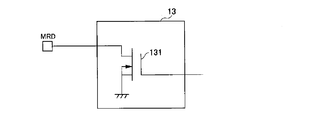
- FIG. 2 shows an example of the configuration of the relay drive circuit 13.
- the relay drive circuit 13 can be configured by using a switching element 131 such as a MOSFET (Metal Oxide Semiconductor Field Effect Transistor).
- FIG. 2 shows an example in which an N-channel MOSFET is used for the switching element 131.
- the gate of the switching element 131 is connected to the terminal PSA, the drain is connected to the terminal MRD, and the source is grounded.
- the power supply voltage VBAT is supplied to the gate via the terminal PSA, the drain and source are in a conductive (on) state, a current flows through the coil 12a, and the contact 12b is turned on.
- FIG. 2 is for explaining the basic function of the relay drive circuit 13, and is not limited to this configuration.
- the first power supply circuit 21 is characterized in that the power supply voltage VBAT supplied from the terminal VB is input and its operation is controlled depending on whether or not the power supply voltage VBAT is applied via the terminal PSA.
- the first power supply circuit 21 sets the internal voltage V1 to the second power supply system block 120. It also has a function of outputting to the microcomputer 102. Further, the first power supply circuit 21 has a function of not outputting the internal voltage V1 when the power supply voltage VBAT is not supplied via the terminal VB or when the power supply voltage VBAT is not applied via the terminal PSA.
- the second power supply circuit 22 has a function of inputting the power supply voltage VBAT supplied via the terminal BATT and outputting the internal voltage V2 to the second power supply system block 120.
- the second power supply circuit 22 has a function of outputting the internal voltage V2 to the second power supply system block 120.
- the internal voltage V2 is not output.
- the second power supply circuit 22 operates by the power supply voltage VBAT directly supplied from the battery 10 by the path (terminal BATT) not passing through the power supply relay 12.
- the second power supply circuit 22 is supplied with the power supply voltage VBAT regardless of whether the power supply relay 12 is turned on or off.
- the voltage detection circuit 30 has a function of outputting the result of detecting the power supply voltage VBAT supplied from the terminal VB as VBdet.
- the voltage level of VBdet is a binary value of high level (hereinafter "H level”) or low level (hereinafter "L level”).
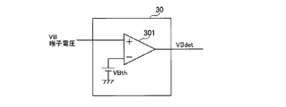
- FIG. 3 shows an example of the configuration of the voltage detection circuit 30.
- the voltage detection circuit 30 includes a comparator 301 and a constant voltage circuit that generates a threshold voltage VBth.
- the wiring VB is connected to the non-inverting input terminal (+ terminal) of the comparator 301, and the threshold voltage VBth is input to the inverting input terminal (-terminal) of the comparator 301.
- the comparator 301 outputs the H level voltage detection result VBdet when the power supply voltage VBAT (first power supply voltage) input from the terminal VB is larger than the threshold voltage VBth.
- the communication circuit 40 is connected to the microcomputer 102 and the register 31, and writes H-level or L-level binary information to the register 31 according to an instruction from the microcomputer 102, or reads out the binary information held by the register 31 to read the microcomputer. It has a function of transmitting to 102.
- the register 31 (an example of the storage unit) is connected to the voltage detection circuit 30 and the communication circuit 40, and when the output VBdet of the voltage detection circuit 30 is H level, it is written from the microcomputer 102 via the communication circuit 40. Holds binary information. Further, the register 31 always holds only the L level information when the output VBdet of the voltage detection circuit 30 is the L level.
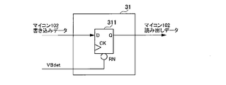
- FIG. 4 shows an example of the configuration of the register 31.
- the register 31 is composed of, for example, a D-type flip-flop 311. Data written from the microcomputer 102 is input to the input terminal D of the D-type flip-flop 311 via the communication circuit 40, and the held data is output from the output terminal Q.
- the output VBdet of the comparator 301 is input to the reset terminal RN of the D-type flip-flop 311.
- the reset terminal RN is an inverting input.
- the clock signal generated by the second power supply system block 120 is input to the clock terminal.
- the D-type flip-flop 311 While the L level signal is input to the reset terminal RN, the D-type flip-flop 311 is in the reset state, and the value to be held is always the L level. While the H level signal is input to the reset terminal RN, the D-type flip-flop 311 is in the non-reset state, and in the present embodiment, the H level or L level written from the microcomputer 102 via the communication circuit 40. Hold data.
- the register 31 (an example of the storage unit) holds and outputs the information written by the processor (processor 102a), and inverts the low-level signal output by the voltage detection circuit (voltage detection circuit 30). Is configured to reset the retained information and output a low-level signal.
- the microcomputer 102 operates when the internal voltage V1 is supplied from the first power supply circuit 21, and has a function of writing binary information to the register 31 or reading binary information from the register 31 via the communication circuit 40. ..
- the microcomputer 102 includes a processor 102a such as a CPU, a memory 102b such as a RAM or a ROM, and the like.
- the processor 102a is the main body of operation of the microcomputer 102.
- a noise removing circuit or the like is often provided between the microcomputer 102 and the wiring to which the internal voltage V1 is supplied.
- the microcomputer 102 can read the register value and detect the sticking of the power supply relay 12.
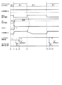
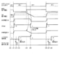
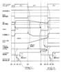
- FIG. 5 is a timing chart showing an example of operation when the power relay 12 is not fixed on in the electronic control device 100.
- On-sticking means that the contact 12b of the power relay 12 is stuck in the on state and does not change to the off state. Off sticking is the opposite. On-sticking occurs due to a failure such as contact welding of the power supply relay 12 or a ground short circuit on the output side (drain-source of the switching element 131) of the relay drive circuit 13.
- An example of timing is shown.
- the horizontal axis of this timing chart represents the passage of time.
- the ignition switch 11 is in the off state at the initial time t0 of the timing chart shown in FIG.
- the potential of the terminal MRD connected to the relay drive circuit 13 is substantially equal to the power supply voltage VBAT, and the power supply relay 12 is controlled to be in the off state. That is, the power supply voltage VBAT is not supplied to the terminal VB.
- the internal voltage V1 is not output from the first power supply circuit 21, and the communication circuit 40 and the microcomputer 102 are in a non-operating state.
- the power supply voltage VBAT is supplied to the terminal BATT, and the second power supply circuit 22 outputs the internal voltage V2 and supplies it to the second power supply system block 120.
- the voltage detection circuit 30 and the register 31 included in the second power supply system block 120 are in a state in which they can be electrically operated.
- the output VBdet of the voltage detection circuit 30 outputs the L level, the register 31 is reset, and the L level is held.
- the power supply voltage VBAT is supplied to the terminal PSA via the ignition switch 11, the switching element 131 of the relay drive circuit 13 is turned on, a current is drawn from the terminal MRD, and the power supply relay 12 is turned on.
- the power supply voltage VBAT is supplied to the terminal VB, and the first power supply circuit 21 outputs the internal voltage V1.
- the communication circuit 40 and the microcomputer 102 start operation by receiving the supply of the internal voltage V1.
- the power supply voltage VBAT is also supplied to the voltage detection circuit 30, and when the power supply voltage VBAT exceeds the threshold voltage VBth, the output VBdet changes from the L level to the H level.
- the register 31 changes from the reset state to the non-reset state when the output VBdet of the voltage detection circuit 30 becomes H level.
- the microcomputer 102 reads out the data held in the register 31 (D-type flip-flop 311) via the communication circuit 40.
- the data held in the register 31 at time t2 is at the L level, and the read data is also at the L level.
- the microcomputer 102 performs a predetermined process such as initialization between the time t1 and the time t2, and promptly executes data reading after the predetermined process is completed.
- the microcomputer 102 writes H-level data to the register 31 (D-type flip-flop 311) via the communication circuit 40, and the H-level data is held in the register 31.
- the microcomputer 102 After that, after switching the ignition switch 11 on again at time t6, the same operation as when the ignition switch 11 is turned on at time t1 is performed. At time t7, similarly to time t2, the microcomputer 102 reads L-level data from the register 31 via the communication circuit 40. Then, at time t8, the microcomputer 102 writes H-level data to the register 31 in the same manner as at time t3 in preparation for the next sticking detection.
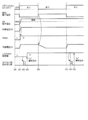
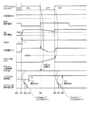
- FIG. 6 is a timing chart showing an example of the operation when the power relay 12 is fixed on in the electronic control device 100.
- the on / off of the power relay 12 could be controlled up to time t3 as in FIG. 5, but the power relay 12 stuck in the on state after time t3 until time t10.
- the explanation will be made assuming a case. Since the operation from the initial time t0 to the time t3 is the same as the example shown in FIG. 5, the description thereof will be omitted.
- the power relay 12 is stuck in the on state.
- the power supply voltage VBAT continues to be supplied to the terminal VB of the electronic control device 100.
- the power supply voltage VBAT continues to be supplied to the first power supply circuit 21, but since the voltage is not applied via the terminal PSA by turning off the ignition switch 11, the first power supply circuit 21 has an internal voltage of V1. Stop the output. Therefore, the communication circuit 40 and the microcomputer 102 stop operating because the supply of the internal voltage V1 is stopped.
- the second power supply circuit 22 receives the supply of the power supply voltage VBAT via the terminal BATT and outputs the internal voltage V2 regardless of whether or not the power supply relay 12 is stuck, so that the voltage detection circuit 30 continues to operate.
- the output VBdet remains at the H level. Therefore, the register 31 holds the H level data written from the microcomputer 102 at the time t3.
- the power supply voltage VBAT is applied to the first power supply circuit 21 via the terminal PSA. Then, the first power supply circuit 21 outputs the internal voltage V1 based on the power supply voltage VBA, and the communication circuit 40 and the microcomputer 102 start operating.
- the microcomputer 102 reads out the data held in the register 31 via the communication circuit 40.
- the microcomputer 102 since the register 31 holds the H level data, the microcomputer 102 reads the H level data. That is, by assuming the case where the power relay 12 is stuck in the ON state, H level data different from the L level data read at time t2 is read. By reading the H level data from the register 31 in this way, the microcomputer 102 can detect that the power relay 12 is stuck in the ON state.
- the microcomputer 102 writes H-level data to the register 31 in the same manner as at time t8.
- the configuration and method for realizing the electronic control device 100 capable of detecting that the power relay 12 is stuck in the ON state have been clarified.
- the electronic control device controls the on / off of the power relay (power relay 12) according to the on / off information of the power supply (ignition switch 11).
- the electronic circuit first power supply
- the electronic circuit that operates with the relay drive circuit (relay drive circuit 13) of the above and the first power supply voltage (power supply voltage VBAT via the terminal VB) supplied from the battery (battery 10) via the power supply relay.
- a monitoring unit (second power supply system block) that monitors the first power supply voltage when the power is off and holds the monitoring result, which reflects the presence or absence of sticking between the system block 110 and the microcomputer 102). 120) and so on.
- the monitoring unit detects and holds the state in which the power supply to the electronic control device cannot be cut off due to the power relay being stuck in the on state. Then, after the power is turned on, the monitoring result (read data) including the information about the sticking of the power relay is read from the monitoring unit, and the monitoring result is notified to the user of the vehicle to encourage the user to take necessary measures. Can be done.
- the monitoring result read data
- the monitoring result is notified to the user of the vehicle to encourage the user to take necessary measures. Can be done.
- the electronic control device even when the power relay cannot be turned off and the power supply to the monitoring unit is normally cut off, the presence or absence of the power relay is stuck. Based on the reflected first power supply voltage monitoring result, the sticking of the power supply relay can be detected.
- the monitoring unit responds to the voltage value of the first power supply voltage (power supply voltage VBAT via the terminal VB).
- the voltage detection circuit (voltage detection circuit 30) that outputs a signal of the same level (H, L) and the first power supply voltage based on the signal output by the voltage detection circuit when the power supply (ignition switch 11) is off.
- a storage unit (register 31) that holds information indicating the presence or absence of a decrease as the monitoring result is provided.
- the storage unit holds information indicating whether or not the first power supply voltage is lowered based on the signal output by the voltage detection circuit, thereby responding to a request for reading information from the outside.
- the information can be output.
- the electronic circuit (first power supply system block 110, microcomputer 102) has a first power supply voltage (register 31) held in the storage unit (register 31).
- a processor (processor 102a) for reading information indicating the presence or absence of a decrease in the power supply voltage VBAT) via the terminal VB and writing information to the storage unit is provided.
- the processor is configured to detect a sticking abnormality of the power supply relay (power supply relay 12) based on the information read from the storage unit.
- the processor reads out the information held in the storage unit indicating whether or not the first power supply voltage has dropped at an arbitrary timing, and detects the sticking abnormality of the power supply relay. be able to.
- the voltage detection circuit sets the first power supply voltage (power supply voltage VBAT via the terminal VB) to the threshold voltage (VBth).
- VBth threshold voltage
- a high level signal is output to the storage unit (register 31), and in other cases, a low level signal is output.
- the voltage detection circuit outputs a high level signal to the storage unit when the first power supply voltage is larger than the threshold voltage, and outputs a low level signal in other cases.
- Information indicating a high level or information indicating a low level is stored in the storage unit.
- the processor reads out to the storage unit (register 31) when the power supply (ignition switch 11) is switched from off to on. Based on the first read information read from the storage unit last time (time t2) and the second read information read from the storage unit this time (time t7, t12), the power relay (power relay 12) ) Is configured to detect sticking abnormalities.
- the electronic control device having the above configuration, when the power is switched from off to on, the first read information read last time from the storage unit and the second read information read from the storage unit this time (after turning on again). It is possible to compare the information and detect the sticking abnormality of the power supply relay from the comparison result.
- the processor is information that the first read information read from the storage unit last time (time t2) indicates a low level, and When the second read information read from the storage unit this time (time t7, t12) is information indicating a high level, the power relay (power relay 12) is configured to determine that the sticking is abnormal. There is.
- the first read information read last time from the storage unit is the information indicating the low level
- the second read information read from the storage unit this time (after re-on) is high.
- the information changes to indicate the level it can be determined that the first power supply voltage has not dropped to the voltage threshold value, that is, an abnormality in sticking of the power supply relay has occurred.
- the processor reads information from the storage unit (register 31) when the power supply (ignition switch 11) is turned from off to on. , After reading the information from the storage unit, the information indicating the high level is written in the storage unit.
- the electronic control device having the above configuration, when the power is turned on from off, the information is read from the storage unit, and then the information indicating the high level is written to the storage unit, so that the power is then turned on from off. It is possible to detect a sticking abnormality of the power relay from the change of the information held in the storage unit when the value becomes.
- the monitoring unit (second power supply system block 120) is provided by a path (path via the terminal BATT) that does not pass through the power supply relay (power supply relay 12). It operates by the second power supply voltage (power supply voltage VBAT via the terminal BATT) supplied from the battery (battery 10).
- the monitoring unit is supplied with the second power supply voltage directly from the battery without being affected by the on / off (sticking) of the power supply relay.
- Second embodiment> In the second embodiment, another example of the configuration and operation of the electronic control device capable of detecting that the power relay 12 is stuck in the ON state will be described.
- FIG. 7 is a block diagram showing an example of the configuration of the electronic control device 100A according to the second embodiment.
- the difference between the electronic control device 100A according to the second embodiment and the electronic control device 100 according to the first embodiment will be described.
- the electronic control device 100A shown in FIG. 7 is different from the electronic control device 100 (FIG. 1) according to the first embodiment in that the second power supply circuit 22 receives the power supply voltage VBAT supplied via the terminal VB as an input. ..
- the power supply voltage VBAT first power supply voltage
- the power supply voltage VBAT supplied to the second power supply circuit 22 can be turned on / off by the contact 12b of the power supply relay 12.
- the power supply voltage VBAT supplied to the second power supply circuit 22 is affected by the sticking of the power supply relay 12 (contact 12b).
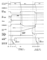
- FIG. 8 is a timing chart showing an example of operation when the power relay 12 is not fixed on in the electronic control device 100A.
- the items described in the timing chart of FIG. 5 are the state at the initial time t0 of FIG. 5 and the state at the initial time t20 of FIG. Are the same.
- the relay drive circuit 13 is turned on and the relay drive circuit 13 turns on the power relay 12.
- the power supply voltage VBAT is supplied to the terminal VB
- the first power supply circuit 21 outputs the internal voltage V1
- the second power supply circuit 22 outputs the internal voltage V2.
- the voltage detection circuit 30 and the register 31 start operation by receiving the supply of the internal voltage V2. Further, the voltage detection circuit 30 inputs the power supply voltage VBAT via the terminal VB, and when the power supply voltage VBAT exceeds the threshold voltage VBth, the output VBdet changes from the L level to the H level.
- the register 31 changes from the reset state to the non-reset state when the output VBdet of the voltage detection circuit 30 becomes H level.
- the microcomputer 102 reads out the data held in the register 31 via the communication circuit 40.
- the data held in the register 31 at time t22 is at the L level, and the read data is also at the L level.
- the microcomputer 102 writes H-level data to the register 31 via the communication circuit 40, and the H-level data is held in the register 31.
- the relay drive circuit 13 is turned off. Therefore, the voltage of the terminal VB (first power supply voltage) gradually decreases due to the current consumption of the electronic control device 100. As the voltage of the terminal VB decreases, the internal voltage V2 cannot maintain the voltage required for the operation of the voltage detection circuit 30 and the data retention of the register 31.
- the register 31 stops operating, and the output of the register 31 is fixed (reset) to the L level.
- the output VBdet of the voltage detection circuit 30 changes to the L level, the register 31 is reset, and the register 31 is reset.
- the retained data may be changed to the L level.
- the microcomputer 102 After that, after switching the ignition switch 11 on again at time t26, the same operation as when the ignition switch 11 is turned on at time t21 is performed. At time t27, similarly to time t22, the microcomputer 102 reads L-level data from the register 31 via the communication circuit 40. Then, at time t28, the microcomputer 102 writes H-level data to the register 31 in the same manner as at time t23.
- FIG. 9 is a timing chart showing an example of the operation when the power relay 12 is fixed on in the electronic control device 100A.
- the on / off of the power relay 12 could be controlled from the initial time t20 to the time t23 as in FIG. 8, but the power relay 12 is turned on after the time t23 until the time t30.
- the description will be made on the assumption that the particles are stuck in a state. Since the operation from the initial time t20 to the time t23 is the same as the example shown in FIG. 8, the description thereof will be omitted.
- the power relay 12 is stuck in the on state.
- the power supply voltage VBAT continues to be supplied to the terminal VB of the electronic control device 100.
- the power supply voltage VBAT continues to be supplied to the first power supply circuit 21, but since the voltage is not applied via the terminal PSA by turning off the ignition switch 11, the first power supply circuit 21 has an internal voltage of V1. Stop the output. Therefore, the communication circuit 40 and the microcomputer 102 stop operating because the supply of the internal voltage V1 is stopped.
- the second power supply circuit 22 receives the supply of the power supply voltage VBAT via the fixed power supply relay 12 and continues to output the internal voltage V2, the voltage detection circuit 30 continues to operate and the output VBdet is H level. Remains. Therefore, the register 31 holds the H level data written from the microcomputer 102 at the time t23.
- the power supply voltage VBAT is applied to the first power supply circuit 21 via the terminal PSA, the first power supply circuit 21 outputs the internal voltage V1, and the communication circuit 40 and the communication circuit 40.
- the microcomputer 102 starts operation.
- the microcomputer 102 reads out the data held in the register 31 via the communication circuit 40.
- the microcomputer 102 since the register 31 holds the H level data, the microcomputer 102 reads the H level data. That is, by assuming the case where the power relay 12 is stuck in the ON state, H level data different from the L level data read at time t22 is read. In this way, as in the first embodiment, the microcomputer 102 reads the H level data from the register 31, so that the microcomputer 102 can detect that the power relay 12 is stuck in the ON state. Become.
- the microcomputer 102 writes H-level data to the register 31 in the same manner as at time t28.
- the second power supply circuit 22 is different from the first power supply circuit 21 in that the power supply voltage VBAT is supplied via the terminal BATT.
- the difference is whether to receive the power supply voltage VBAT from the terminal VB via the power supply relay 12 as in the first power supply circuit 21. That is, in other words, it was shown that even when the second power supply circuit 22 is supplied with power by the same route as the first power supply circuit 21, it is possible to detect the on-sticking of the power supply relay 12.
- the monitoring unit (second power supply system block 120) is based on the first power supply voltage (power supply voltage VBAT via the terminal VB). Operate.
- the monitoring unit operates at the first power supply voltage (power supply voltage VBAT) supplied from the battery (battery 10) via the power supply relay (power supply relay 12).
- the monitoring unit is affected by the on / off (sticking) of the power relay 12.
- the power supply is supplied. The sticking of the power relay can be detected based on the monitoring result of the first power supply voltage reflecting the presence or absence of the sticking of the relay.
- the voltage of the terminal VB is detected because the power relay 12 is detected to be on and stuck, and the ignition off period is short even though the power relay 12 is not actually stuck.
- An example of the configuration and operation of the electronic control device for preventing erroneous detection that the power relay 12 is stuck when the ignition switch 11 is turned on again before the voltage falls below the threshold voltage VBth will be described.
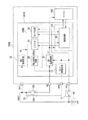
- FIG. 10 is a block diagram showing an example of the configuration of the electronic control device 100B according to the third embodiment.
- the difference between the electronic control device 100B according to the third embodiment and the electronic control device 100 according to the first embodiment will be described.
- the electronic control device 100B shown in FIG. 10 is for measuring the off time from the time when the ignition switch 11 is further switched from the on state to the off state in the second power supply system block 120B which is operated by supplying the internal voltage V2.
- a timer circuit 32 is provided. That is, the third embodiment is a configuration in which the timer circuit 32 is provided in the configuration of the first embodiment.
- the timer circuit 32 is connected to the communication circuit 40 and the wiring PSA, and measures the time in a state where the power supply voltage VBAT is not supplied to the wiring PSA.
- the microcomputer 102 can read the time information measured by the timer circuit 32 via the communication circuit 40 from the timer circuit 32.
- FIG. 11 is a block diagram showing an example of the configuration of the timer circuit 32.
- the timer circuit 32 compares the counter 321 that periodically increases and outputs the count value CNT by a clock signal (not specified), the count threshold value CNTth, and the count value CNT and the count threshold value CNTth. It is composed of a count comparison circuit 322.
- the count comparison circuit 322 outputs the count comparison result CNTd to the communication circuit 40 as binary information of H level or L level.
- the counter 321 fixes the count value CNT to zero when the potential of the PSA terminal is the power supply voltage VBAT, and periodically counts the count value by a clock signal (not shown) when the potential of the PSA terminal is the ground potential. Increase CNT.
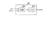
- FIG. 12 is a block diagram showing an example of the configuration of the count comparison circuit 322 included in the timer circuit 32.
- the count comparison circuit 322 includes a comparator 322a that compares the count value CNT of the counter 321 with the count threshold CNTth and outputs the comparison result, and a register 322b that holds the comparison result output by the comparator 322a.
- the comparator 322a outputs H level data as the count comparison result CNTd when the count value CNT is larger than the count threshold CNTth, and outputs L level data as the count comparison result CNTd in other cases.
- the comparator 322a can be configured by a comparator.
- the microcomputer 102 can read the count comparison result CNTdet from the register 322b of the timer circuit 32 via the communication circuit 40, and can write a desired value to the count threshold value CNTth.
- the count threshold value CNTth is stored in a register or a memory included in the timer circuit 32.
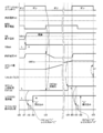
- FIG. 13 is a timing chart showing an example of the operation when the power relay 12 is not fixed on in the electronic control device 100B.
- the power relay 12 can be normally controlled to the on or off state and the off period of the ignition switch 11 is sufficiently long. Specifically, consider a case where the ignition switch 11 is turned on again after the ignition switch 11 is turned off and the voltage of the terminal VB falls below the threshold voltage VBth.
- the state at the initial time t0 of FIG. 5 and the state at the initial time t40 of FIG. 13 are the same.
- the operations from the initial time t40 to the time t44 are basically the same.
- the count value CNT of the counter 321 is zero and the count comparison result CNTtet is the L level in the initial state at the initial time t20.
- the operation of the electronic control device 100B at this time is the same as the operation at time t1 described in the first embodiment (FIG. 5). That is, the power supply voltage VBAT is supplied to the terminal PSA via the ignition switch 11, and the relay drive circuit 13 turns on the power supply relay 12. When the power relay 12 is turned on, the power supply voltage VBAT is supplied to the terminal VB, and the first power supply circuit 21 outputs the internal voltage V1.
- the communication circuit 40 and the microcomputer 102 start operation by receiving the supply of the internal voltage V1.
- the power supply voltage VBAT is also supplied to the voltage detection circuit 30, and when the power supply voltage VBAT exceeds the threshold voltage VBth, the output VBdet changes from the L level to the H level.
- the register 31 changes from the reset state to the non-reset state when the output VBdet becomes H level.
- the microcomputer 102 reads out the data held in the register 31 via the communication circuit 40 and the count comparison result CNTt held in the register 322b of the timer circuit 32.
- the data held in the register 31 is set to the L level
- the count comparison result CNTdet is also set to the L level in the initial state. Therefore, regarding the data read by the microcomputer 102 at time t42, both the holding data in the register 31 and the count comparison result CNTdet are at the L level.
- the microcomputer 102 writes H-level data to the register 31 via the communication circuit 40, and the H-level data is held in the register 31.
- the relay drive circuit 13 is turned off. Therefore, the voltage of the terminal VB (first power supply voltage) gradually decreases due to the current consumption of the electronic control device 100B.
- the voltage drop rate of the terminal VB shown in FIG. 13 is slower than the voltage drop rate of the terminal VB shown in FIG.
- the timer circuit 32 (counter 321) starts measuring the off time of the ignition switch 11 and initializes the count comparison result CNTet to the L level.
- the initial state of the count comparison result CNTet is described as the L level, the value of the count comparison result CNTt does not change before and after the writing is performed at time t43.
- the microcomputer 102 reads out the data held in the register 31 via the communication circuit 40 and the count comparison result CNTdet output by the timer circuit 32.
- the difference between the time t42 and the time t48 is that the H level is read out to the microcomputer 102 as the data of the count comparison result CNTd when the count value CNT of the timer circuit 32 reaches the count threshold value CNTth at the time t46.
- the microcomputer 102 writes H-level data to the register 31 in the same manner as at time t43. From the above, in the timing chart of FIG. 13, since the read data of the register 31 after the ignition switch 11 is turned on again is the L level, it can be determined that the power relay 12 is normally turned off.
- FIG. 14 is a timing chart showing an example different from that of FIG. 13 in the operation when the power relay 12 is not fixed on in the electronic control device 100B.
- the power relay 12 can be normally controlled to the on or off state and the off period of the ignition switch 11 is short. Specifically, consider a case where the ignition switch 11 is turned on again after the ignition switch 11 is turned off and before the voltage of the terminal VB falls below the threshold voltage VBth. At this time, it is assumed that the count value CNT of the timer circuit 32 that counts the off period of the ignition switch 11 is before the count threshold value CNT th is reached. Since the operation from the initial time t40 to the time t44 in FIG. 14 is the same as the example shown in FIG. 13, the description thereof will be omitted.
- the microcomputer 102 reads out the data held in the register 31 via the communication circuit 40 and the count comparison result CNTdet output by the timer circuit 32. Then, at time t52, the microcomputer 102 writes H-level data to the register 31 in the same manner as at time t43.
- the difference between the time t51 and the time t48 in FIG. 13 is that the H level data was read from the register 31 even though the power relay 12 was not stuck on. That is, in the first embodiment, it is determined that the power relay 12 is in the on-fixed state when the data read from the register 31 is at the H level.
- the timing chart of FIG. 14 suggests that there is a possibility of erroneously diagnosing the on-sticking of the power relay 12 depending on the time from turning off the ignition switch 11 to turning it on again.
- the timer circuit 32 is arranged and the off period of the ignition switch 11 is measured before the voltage of the terminal VB falls below the threshold voltage VBth of the voltage detection circuit 30.
- the ignition switch 11 is turned on again, it is possible to prevent the power relay 12 from being erroneously diagnosed as being stuck on.
- the microcomputer 102 reads the L level in the count comparison result CNTet of the timer circuit 32, even if the microcomputer 102 reads the H level data from the register 31, it is ignored, and the power relay 12 is in the ON-fixed state. Judge that it is not.
- FIG. 15 is a timing chart showing an example of the operation when the power relay 12 is fixed on in the electronic control device 100B.
- the on / off of the power relay 12 could be controlled from the initial time t40 to the time t43 in the same manner as in FIG. 13, but the power relay 12 is turned on after the time t43 until the time t53.
- the description will be made on the assumption that the particles are stuck in a state. Since the operation from the initial time t40 to the time t43 is the same as the example shown in FIG. 13, the description thereof will be omitted.
- the power relay 12 When the ignition switch 11 is switched from on to off at time t53 after the power relay 12 is stuck in the on state between the time t43 and the time t53, the power relay 12 is stuck in the on state and is electronic.
- the operation of the control device 100B is the same as the operation at time t10 described in the first embodiment (FIG. 6).
- the difference between the operation at time t53 and the operation at time t10 shown in FIG. 6 in this embodiment is that the timer circuit 32 starts measuring the off time of the ignition switch 11 and initializes the count comparison result CNTet to the L level. Is.
- the initial state of the count comparison result CNTdet is described as the L level, so that the value of the count comparison result CNTdet does not change before and after the writing is performed at the time t43. ..
- the power supply voltage VBAT is applied to the first power supply circuit 21 via the terminal PSA. Then, the first power supply circuit 21 outputs the internal voltage V1, and the communication circuit 40 and the microcomputer 102 start operating.
- the microcomputer 102 reads out the data held in the register 31 via the communication circuit 40 and the count comparison result CNTdet output by the timer circuit 32.
- the holding data and the count comparison result CNTet of the register 31 are at the H level, and the microcomputer 102 reads the H level data as the holding data and the count comparison result CNTet of the register 31.
- the microcomputer 102 writes H-level data to the register 31 in the same manner as at time t43.
- FIG. 15 is different from FIG. 14 in that the count value CNT of the timer circuit 32 exceeds the count threshold value CNTth during the off period of the ignition switch 11, and the count comparison result CNTtet is at the H level.
- a desired value can be written from the microcomputer 102 via the communication circuit 40. Then, as shown in FIG. 13, after the voltage of the terminal VB after the ignition switch 11 is turned off falls below the threshold voltage VBth of the voltage detection circuit 30, the count output CNT of the timer circuit 32 is appropriate to exceed the count threshold CNTth. Set to. Thereby, this embodiment can be used as a means for preventing erroneous diagnosis of on-sticking of the power relay 12.
- the microcomputer 102 reads the holding data of the register 31 and the count comparison result CNTdet via the communication circuit 40 after the ignition switch 11 is turned on in a state where the count threshold value CNTth is appropriately set. It can be determined that the power supply relay 12 is stuck on only when all the read data are at the H level.
- the processor (processor 102a) further measures the time when the power supply (ignition switch 11) is off, which is a timer circuit (timer circuit). 32). Then, in the processor (processor 102a), the measurement time (count value CNT) of the timer circuit is such that the first power supply voltage (power supply voltage VBAT via the terminal VB) falls below the threshold voltage (VBth) after the power is turned off. When it is equal to or less than the threshold value (count threshold voltage CNTth) set based on the time required until, control is performed so as not to detect the sticking abnormality of the power supply relay (power supply relay 12).
- the threshold value is set based on the time required for the power-off time (measurement time) from the time when the power is turned off until the first power supply voltage falls below the threshold voltage.
- the power relay sticking abnormality is not detected.
- the sticking abnormality detection is not performed, so that the false detection of the sticking abnormality of the power relay can be prevented.
- the measurement time of the timer circuit is first after the power supply (ignition switch 11) is turned off.
- the power supply voltage power supply voltage VBAT via the terminal VB
- the timer count threshold CNTth
- the storage unit register 31
- the electronic control device having the above configuration, after confirming that the first power supply voltage has definitely dropped to the threshold voltage, the power supply relay sticking abnormality is detected based on the information read from the storage unit. , It is possible to prevent false detection of sticking abnormality of the power relay.
- FIG. 16 is a timing chart showing another example of operation when the power relay is fixed on in the electronic control device according to the modified example of the third embodiment.
- the operations from the initial time t40 to the time t43 and from the time t53 to the time t54 are the same as the examples shown in FIG. 13, and thus the description thereof will be omitted.
- the power supply voltage VBAT is applied to the first power supply circuit 21 via the terminal PSA. Then, the first power supply circuit 21 outputs the internal voltage V1, and the communication circuit 40 and the microcomputer 102 start operating.
- the count value CNT of the timer circuit 32 is returned to zero by turning on the ignition switch 11, but in the example of FIG. 16, the count value CNT is not reset.
- the ignition switch 11 is turned on, the count value CNT of the counter 321 at that time is held.
- the microcomputer 102 reads out the data held in the register 31 via the communication circuit 40. Then, the microcomputer 102 determines whether or not the power supply relay 12 is stuck based on the read data of the register 31 and the count comparison result CNTdet. Then, at time t62, the microcomputer 102 writes H-level data to the register 31 in the same manner as at time t43.
- the first to third embodiments described above describe the configuration of the electronic control device in detail and concretely in order to aid the understanding of the present invention, and are not necessarily limited to those including all the components described above. Not done. It is also possible to add, replace, or delete other components with respect to a part of the components of each embodiment.
- the count threshold value CNTth is configured to be writable by the microcomputer 102 via the communication circuit 40, and only the count comparison result CNTdet is read from the timer circuit 32. It was configured.
- the microcomputer 102 may read the count value CNT which is the output of the counter 321 of the timer circuit 32 via the communication circuit 40, compare it with the threshold value set inside the microcomputer 102, and determine the off period.
- a VB wiring is connected to the non-inverting input terminal of the comparator 301, and the threshold voltage VBth is input to the inverting input terminal to compare the voltages.
- the threshold voltage VBth is input to the inverting input terminal to compare the voltages.
- each component described in the electronic control device 100 may be an integrated circuit in which all of the components are formed on the same semiconductor chip, or each component may be divided into a plurality of components.
- the first power supply circuit 21, the second power supply circuit 22, the relay drive circuit 13, the communication circuit 40, and the like described as the components of the power supply ICs 101 and 101B are mounted on the electronic control device 100 as separate parts. You may.
- each of the above configurations, functions, processing units, etc. may be realized by hardware, for example, by designing a part or all of them with an integrated circuit.
- FPGA Field Programmable Gate Array
- ASIC Application Specific Integrated Circuit
- each of the above-mentioned components, functions and the like may be realized by software.
- a CPU or other processor 102a provided in the electronic control device reads out a computer program stored in a recording medium (memory 102b) such as a ROM provided inside the electronic control device and sequentially. It may be done by executing.
- control lines and information lines are shown as necessary for explanation, and not all the control lines and information lines are necessarily shown in the product. In practice, it can be considered that almost all components are interconnected.
Landscapes
- Engineering & Computer Science (AREA)
- Mechanical Engineering (AREA)
- Physics & Mathematics (AREA)
- Power Engineering (AREA)
- General Physics & Mathematics (AREA)
- Automation & Control Theory (AREA)
- Electromagnetism (AREA)
- Power Sources (AREA)
- Direct Current Feeding And Distribution (AREA)
- Keying Circuit Devices (AREA)
Abstract
Description
このため、電源リレーのオン固着異常を検出するための異常検出機能を電子制御装置に設けて、オン固着異常が生じた場合にユーザに対し何らかの処置が実施できるよう促すことが求められる。例えば特許文献1には、イグニッションスイッチのオフの状態でマイクロコンピュータ(以下「マイコン」と略記する。)が起動した回数を計測し、計測値に基づいて電源リレーのオン固着異常の有無を判定する電子制御装置が記載されている。
上記した以外の課題、構成及び効果は、以下の実施形態の説明により明らかにされる。
まず、本発明の第1の実施形態に係る電子制御装置の構成について説明する。
図1は、第1の実施形態に係る電子制御装置100の構成の一例を示すブロック図である。図1に示す電子制御装置100は、電源リレー12の接点12bが固着したことを検知可能に構成されている。電源リレー12は、機械式又は半導体式のいずれでもよい。本明細書では、電源リレー12の接点12bが固着することを「電源リレー12が固着する」と記載する。また、後述する説明において、電源リレー12の接点12bがオン(閉)/オフ(開)することを「電源リレー12がオン/オフする」と記載する。
リレー駆動回路13は、MOSFET(Metal Oxide Semiconductor Field Effect Transistor)等のスイッチング素子131を用いて構成することができる。図2は、スイッチング素子131に、Nチャネル型のMOSFETを用いた例である。スイッチング素子131のゲートは端子PSAに接続され、ドレインは端子MRDに接続され、ソースが接地されている。ゲートに端子PSAを介して電源電圧VBATが供給されるとドレイン-ソース間が導通(オン)状態となり、コイル12aに電流が流れて接点12bがオンする。一方、ゲートに電源電圧VBATが供給されないと、ドレイン-ソース間が非導通(オフ)状態となり、コイル12aに電流が流れず接点12bはオフする。なお、図2の例は、リレー駆動回路13の基本機能を説明するためのものであり、この構成に限らない。
例えば、電圧検知回路30は、コンパレータ301と、閾値電圧VBthを生成する定電圧回路から構成される。配線VBはコンパレータ301の非反転入力端子(+端子)に接続され、閾値電圧VBthはコンパレータ301の反転入力端子(-端子)に入力される。コンパレータ301は、端子VBより入力される電源電圧VBAT(第1の電源電圧)が閾値電圧VBthよりも大きい場合に、Hレベルの電圧検知結果VBdetを出力する。
レジスタ31は、例えばD型フリップフロップ311から構成される。D型フリップフロップ311の入力端子Dに、通信回路40を介してマイコン102から書き込まれるデータが入力され、保持しているデータが出力端子Qから出力される。コンパレータ301の出力VBdetが、D型フリップフロップ311のリセット端子RNに入力される。リセット端子RNは、反転入力となっている。クロック端子には、例えば第2電源系ブロック120で生成されたクロック信号が入力される。
次に、上述のように構成された電子制御装置100の動作について説明する。まず、図5を参照し、電源リレー12が正常にオン又はオフ状態に制御できる場合を想定して説明する。
次に、電源リレー12が正常にオン又はオフ状態に制御できない場合を説明する。
図6は、電子制御装置100において電源リレー12がオン固着した場合の動作の一例を示すタイミングチャートである。図6に示すタイミングチャートでは、時刻t3までは図5と同様に電源リレー12のオン又はオフを制御できていたが、時刻t3以降で時刻t10までの間に電源リレー12がオン状態で固着した場合を想定して説明する。なお、初期時刻t0から時刻t3までの動作は、図5に示した例と同一であるため説明を省略する。
ここで、電源リレー12が何らかの原因によりオフ状態で固着し、オン状態へ遷移しない場合の電子制御装置100の動作について、図1を参照して説明する。
イグニッションスイッチ11をオフからオンに切り替えて、端子PSAを介してリレー駆動回路13に電源電圧VBATが供給されたにもかかわらず、電源リレー12がオフ状態にある場合は、バッテリ10から供給される電源電圧VBATが電子制御装置100の端子VBへ供給されない。したがって、端子VBを介して供給される電源電圧VBATにより動作する第1電源回路21も、電源電圧VBATの供給を受けない状態となり、第1電源回路21は内部電圧V1を出力しない。すなわち、内部電圧V1の供給により動作する通信回路40及びマイコン102も動作しない。よって、本実施形態にて説明した電子制御装置100の動作は、電源リレー12がオン固着状態にある場合にのみ実現可能である。
第2の実施形態では、電源リレー12がオン状態で固着したことを検知可能な電子制御装置の構成及び動作の、別の一例について説明する。
次に、電子制御装置100Aの動作について説明する。まず、図8を参照し、電源リレー12が正常にオン又はオフ状態に制御できる場合を想定して説明する。
次に、電源リレー12が正常にオン又はオフ状態に制御できない場合を説明する。
図9は、電子制御装置100Aにおいて電源リレー12がオン固着した場合の動作の一例を示すタイミングチャートである。図9に示すタイミングチャートでは、初期時刻t20から時刻t23までは図8と同様に電源リレー12のオン又はオフを制御できていたが、時刻t23以降で時刻t30までの間に電源リレー12がオン状態で固着した場合を想定して説明する。なお、初期時刻t20から時刻t23までの動作は、図8に示した例と同一であるため説明を省略する。
第3の実施形態では、電源リレー12がオン固着したことを検知すると共に、さらに電源リレー12が実際には固着していないにもかかわらず、イグニッションオフの期間が短いために、端子VBの電圧が閾値電圧VBthを下回る前に再度イグニッションスイッチ11がオンされた場合に、電源リレー12が固着したと誤検知することを防止する電子制御装置の構成及び動作の一例について説明する。
タイマ回路32は、例えば図11に示すように、明示しないクロック信号により周期的にカウント値CNTを増加させて出力するカウンタ321と、カウント閾値CNTthと、カウント値CNTとカウント閾値CNTthとを比較するカウント比較回路322から構成される。カウント比較回路322は、カウント比較結果CNTdetをHレベル又はLレベルの二値情報として通信回路40へ出力する
カウント比較回路322は、カウンタ321のカウント値CNTをカウント閾値CNTthと比較してその比較結果を出力する比較器322aと、比較器322aが出力した比較結果を保持するレジスタ322bを備える。比較器322aは、カウント値CNTがカウント閾値CNTthより大きい場合にカウント比較結果CNTdetとしてHレベルのデータを出力し、それ以外の場合にはカウント比較結果CNTdetとしてLレベルのデータを出力する。例えば比較器322aは、コンパレータにより構成することができる。
図13は、電子制御装置100Bにおいて電源リレー12がオン固着しない場合の動作の一例を示すタイミングチャートである。
図14は、電子制御装置100Bにおいて電源リレー12がオン固着しない場合の動作の、図13とは別の例を示すタイミングチャートである。
次に、電源リレー12が正常にオン又はオフ状態に制御できない場合を説明する。
図15は、電子制御装置100Bにおいて電源リレー12がオン固着した場合の動作の一例を示すタイミングチャートである。図15に示すタイミングチャートでは、初期時刻t40から時刻t43までは図13と同様に電源リレー12のオン又はオフを制御できていたが、時刻t43以降で時刻t53までの間に電源リレー12がオン状態で固着した場合を想定して説明する。なお、初期時刻t40から時刻t43までの動作は、図13に示した例と同一であるため説明を省略する。
第3の実施形態では、イグニッションスイッチ11をオンすることで、イグニッションスイッチ11のオフ期間に応じたカウント値CNTを初期化していた。第3の実施形態の変形例として、カウント値CNTを他の方法により初期化する例を説明する。
図13~図15の例では、イグニッションスイッチ11がオンすることによりタイマ回路32のカウント値CNTをゼロに戻していたが、図16の例では、カウント値CNTをリセットしない。イグニッションスイッチ11がオンにより、その時点でのカウンタ321のカウント値CNTが保持される。
なお、本発明は上述した第1~第3の実施形態に限られるものではなく、特許請求の範囲に記載した本発明の要旨を逸脱しない限りにおいて、その他種々の応用例、変形例を取り得ることは勿論である。
例えば、電源IC101,101Bの構成要素として記載した第1電源回路21、第2電源回路22、リレー駆動回路13、及び通信回路40などは、それぞれが別の部品として電子制御装置100に搭載されていてもよい。
Claims (12)
- 電源のオン又はオフの情報に従って電源リレーのオン又はオフを制御するためのリレー駆動回路と、
前記電源リレーを介してバッテリから供給される第1の電源電圧で動作する電子回路と、
前記電源リレーの固着の有無が反映される、前記電源がオフしているときの前記第1の電源電圧を監視し、監視結果を保持する監視部と、備える
電子制御装置。 - 前記監視部は、
前記第1の電源電圧の電圧値に応じたレベルの信号を出力する電圧検知回路と、
前記電源がオフしているときの前記電圧検知回路が出力した信号に基づく前記第1の電源電圧の低下の有無を示す情報を、前記監視結果として保持する記憶部と、を備える
請求項1に記載の電子制御装置。 - さらに、前記電子回路は、
前記記憶部に保持されている前記第1の電源電圧の低下の有無を示す情報の読み出し、及び、前記記憶部に情報の書き込みを行うプロセッサ、を備え、
前記プロセッサは、前記記憶部から読み出した情報に基づき、前記電源リレーの固着異常を検知する
請求項2に記載の電子制御装置。 - 前記電圧検知回路は、前記第1の電源電圧を閾値電圧と比較して、前記第1の電源電圧が前記閾値電圧よりも大きい場合に前記記憶部へハイレベル信号を出力し、それ以外ではローレベル信号を出力する
請求項3に記載の電子制御装置。 - 前記プロセッサは、前記電源がオフからオンに切り替わった場合に前記記憶部に対して読み出しを行い、
前記記憶部から前回読み出した第1の読み出し情報と、前記記憶部から今回読み出した第2の読み出し情報とに基づいて、前記電源リレーの固着異常を検知する
請求項4に記載の電子制御装置。 - 前記プロセッサは、前記記憶部から前回読み出した前記第1の読み出し情報がローレベルを示す情報、且つ、前記記憶部から今回読み出した前記第2の読み出し情報がハイレベルを示す情報である場合には、前記電源リレーが固着異常であると判定する
請求項5に記載の電子制御装置。 - 前記プロセッサは、前記電源がオフからオンになったときに前記記憶部から情報を読み出し、前記記憶部から前記情報を読み出した後、前記記憶部にハイレベルを示す情報を書き込む
請求項6に記載の電子制御装置。 - 前記記憶部は、前記プロセッサにより書き込まれた情報を保持して出力し、前記電圧検知回路が出力するローレベル信号を反転した信号により、保持していた情報をリセットしてローレベル信号を出力するように構成されている
請求項4に記載の電子制御装置。 - 前記監視部は、前記電源リレーを介さない経路によって前記バッテリから供給される第2の電源電圧により動作する
請求項3に記載の電子制御装置。 - 前記監視部は、前記第1の電源電圧により動作する
請求項3に記載の電子制御装置。 - 前記監視部は、さらに前記電源がオフしてからの時間を計測するタイマ回路を備え、
前記プロセッサは、前記タイマ回路の計測時間が、前記電源がオフしてから前記第1の電源電圧が閾値電圧を下回るまでに要する時間を基に設定される閾値以下である場合には、前記電源リレーの固着異常を検知しないようにする制御を行う
請求項9に記載の電子制御装置。 - 前記プロセッサは、前記タイマ回路の計測時間が、前記電源がオフしてから前記第1の電源電圧が閾値電圧を下回るまでに要する時間を基に設定される閾値を超えた場合に、前記記憶部から読み出した情報に基づき、前記電源リレーの固着異常を検知する
請求項11に記載の電子制御装置。
Priority Applications (3)
| Application Number | Priority Date | Filing Date | Title |
|---|---|---|---|
| US17/631,786 US12319210B2 (en) | 2019-09-18 | 2020-08-14 | Electronic control device |
| JP2021546547A JP7288513B2 (ja) | 2019-09-18 | 2020-08-14 | 電子制御装置 |
| CN202080056485.XA CN114223120B (zh) | 2019-09-18 | 2020-08-14 | 电子控制装置 |
Applications Claiming Priority (2)
| Application Number | Priority Date | Filing Date | Title |
|---|---|---|---|
| JP2019169115 | 2019-09-18 | ||
| JP2019-169115 | 2019-09-18 |
Publications (1)
| Publication Number | Publication Date |
|---|---|
| WO2021054007A1 true WO2021054007A1 (ja) | 2021-03-25 |
Family
ID=74883526
Family Applications (1)
| Application Number | Title | Priority Date | Filing Date |
|---|---|---|---|
| PCT/JP2020/030849 Ceased WO2021054007A1 (ja) | 2019-09-18 | 2020-08-14 | 電子制御装置 |
Country Status (4)
| Country | Link |
|---|---|
| US (1) | US12319210B2 (ja) |
| JP (1) | JP7288513B2 (ja) |
| CN (1) | CN114223120B (ja) |
| WO (1) | WO2021054007A1 (ja) |
Citations (4)
| Publication number | Priority date | Publication date | Assignee | Title |
|---|---|---|---|---|
| JP2006347441A (ja) * | 2005-06-17 | 2006-12-28 | Denso Corp | 電子制御装置 |
| JP2009196588A (ja) * | 2008-02-25 | 2009-09-03 | Honda Motor Co Ltd | 車両用制御装置、電気車両及び車両用制御装置の故障検出方法 |
| JP2009234436A (ja) * | 2008-03-27 | 2009-10-15 | Honda Motor Co Ltd | 車両用制御装置、電気車両及び車両用制御装置の故障検出方法 |
| JP2014048070A (ja) * | 2012-08-29 | 2014-03-17 | Denso Corp | 電子制御装置 |
Family Cites Families (3)
| Publication number | Priority date | Publication date | Assignee | Title |
|---|---|---|---|---|
| JP6308486B2 (ja) * | 2012-09-13 | 2018-04-11 | パナソニックIpマネジメント株式会社 | リレー溶着検出装置 |
| JP6146332B2 (ja) * | 2013-09-11 | 2017-06-14 | トヨタ自動車株式会社 | リレーの固着判別システム |
| JP2015217911A (ja) | 2014-05-21 | 2015-12-07 | 株式会社デンソー | 電子制御装置 |
-
2020
- 2020-08-14 CN CN202080056485.XA patent/CN114223120B/zh active Active
- 2020-08-14 JP JP2021546547A patent/JP7288513B2/ja active Active
- 2020-08-14 US US17/631,786 patent/US12319210B2/en active Active
- 2020-08-14 WO PCT/JP2020/030849 patent/WO2021054007A1/ja not_active Ceased
Patent Citations (4)
| Publication number | Priority date | Publication date | Assignee | Title |
|---|---|---|---|---|
| JP2006347441A (ja) * | 2005-06-17 | 2006-12-28 | Denso Corp | 電子制御装置 |
| JP2009196588A (ja) * | 2008-02-25 | 2009-09-03 | Honda Motor Co Ltd | 車両用制御装置、電気車両及び車両用制御装置の故障検出方法 |
| JP2009234436A (ja) * | 2008-03-27 | 2009-10-15 | Honda Motor Co Ltd | 車両用制御装置、電気車両及び車両用制御装置の故障検出方法 |
| JP2014048070A (ja) * | 2012-08-29 | 2014-03-17 | Denso Corp | 電子制御装置 |
Also Published As
| Publication number | Publication date |
|---|---|
| US20220274549A1 (en) | 2022-09-01 |
| JP7288513B2 (ja) | 2023-06-07 |
| CN114223120B (zh) | 2025-04-15 |
| US12319210B2 (en) | 2025-06-03 |
| JPWO2021054007A1 (ja) | 2021-03-25 |
| CN114223120A (zh) | 2022-03-22 |
Similar Documents
| Publication | Publication Date | Title |
|---|---|---|
| US10841071B2 (en) | Data communication system, data communication apparatus, and sensor apparatus | |
| US9476937B2 (en) | Debug circuit for an integrated circuit | |
| US10671467B2 (en) | Semiconductor device | |
| KR100315681B1 (ko) | 반도체집적회로및접촉식ic카드 | |
| KR102860525B1 (ko) | 아날로그 빌트인 셀프 테스트를 수행하는 전자 회로 및 이의 동작 방법 | |
| US8171193B2 (en) | Master communication circuit, slave communication circuit, and data communicating method | |
| JP7288513B2 (ja) | 電子制御装置 | |
| CN101047380B (zh) | 共用输入/输出端子控制电路 | |
| WO2012153516A1 (ja) | 入力回路 | |
| US20140136875A1 (en) | Apparatus and method of controlling clock signals | |
| JP4789972B2 (ja) | データ変換器におけるデータ変換診断ビット | |
| JP5909423B2 (ja) | 半導体装置 | |
| JP5381852B2 (ja) | 不揮発性メモリの電源瞬断対応回路 | |
| JP2015176349A (ja) | 情報処理装置、故障検出方法及びプログラム | |
| CN118866058A (zh) | 一种存储控制装置及存储控制方法 | |
| US8854857B2 (en) | Electronic device and method for FRAM power supply management | |
| US12431893B2 (en) | Information processing device and information processing method | |
| US11557370B2 (en) | Semiconductor device and self-diagnostic method of semiconductor device | |
| JP2021004587A (ja) | 電子制御装置及び車両制御システム | |
| EP3211508A1 (en) | Semiconductor device | |
| CN107025921B (zh) | 存储器装置和用于驱动存储器装置的方法 | |
| JP2008146597A (ja) | バスシステム | |
| US20050110523A1 (en) | Noisy clock test method and apparatus | |
| US20050209715A1 (en) | Monitoring device for monitoring internal signals during initialization of an electronic circuit unit | |
| US20200088771A1 (en) | Semiconductor device |
Legal Events
| Date | Code | Title | Description |
|---|---|---|---|
| 121 | Ep: the epo has been informed by wipo that ep was designated in this application |
Ref document number: 20864833 Country of ref document: EP Kind code of ref document: A1 |
|
| ENP | Entry into the national phase |
Ref document number: 2021546547 Country of ref document: JP Kind code of ref document: A |
|
| NENP | Non-entry into the national phase |
Ref country code: DE |
|
| 122 | Ep: pct application non-entry in european phase |
Ref document number: 20864833 Country of ref document: EP Kind code of ref document: A1 |
|
| WWG | Wipo information: grant in national office |
Ref document number: 202080056485.X Country of ref document: CN |
|
| WWG | Wipo information: grant in national office |
Ref document number: 17631786 Country of ref document: US |