WO2021031293A1 - 一种单极天线带宽调整方法及系统 - Google Patents
一种单极天线带宽调整方法及系统 Download PDFInfo
- Publication number
- WO2021031293A1 WO2021031293A1 PCT/CN2019/108245 CN2019108245W WO2021031293A1 WO 2021031293 A1 WO2021031293 A1 WO 2021031293A1 CN 2019108245 W CN2019108245 W CN 2019108245W WO 2021031293 A1 WO2021031293 A1 WO 2021031293A1
- Authority
- WO
- WIPO (PCT)
- Prior art keywords
- antenna
- matching circuit
- preset
- initial
- antenna matching
- Prior art date
- Legal status (The legal status is an assumption and is not a legal conclusion. Google has not performed a legal analysis and makes no representation as to the accuracy of the status listed.)
- Ceased
Links
Images


Classifications
-
- H—ELECTRICITY
- H01—ELECTRIC ELEMENTS
- H01Q—ANTENNAS, i.e. RADIO AERIALS
- H01Q23/00—Antennas with active circuits or circuit elements integrated within them or attached to them
-
- H—ELECTRICITY
- H01—ELECTRIC ELEMENTS
- H01Q—ANTENNAS, i.e. RADIO AERIALS
- H01Q9/00—Electrically-short antennas having dimensions not more than twice the operating wavelength and consisting of conductive active radiating elements
- H01Q9/04—Resonant antennas
- H01Q9/30—Resonant antennas with feed to end of elongated active element, e.g. unipole
Definitions
- the invention relates to the technical field of antenna bandwidth adjustment, in particular to a monopole antenna bandwidth adjustment method and system.
- Bluetooth headsets are loved by users because of their convenience.
- the appearance of the bluetooth headset is rich and diverse, and the design of the bluetooth antenna is changed accordingly to adapt to the appearance of the bluetooth headset.
- the Bluetooth headset is usually a monopole antenna.
- the bandwidth of the monopole antenna is required to meet the antenna bandwidth requirement (2402MHz-2480MHz).
- the monopole antenna bandwidth can only be adjusted according to the experience of the engineer, and then the bandwidth of the adjusted monopole antenna is detected, and the monopole antenna is adjusted according to the detected bandwidth. Repeat the above process until the bandwidth of the monopole antenna meets the antenna bandwidth requirement. The adjustment period of this adjustment method is longer, and the antenna bandwidth optimization performance is low.
- the purpose of the present invention is to provide a monopole antenna bandwidth adjustment method and system, which realizes the advance prediction of the monopole antenna bandwidth and resonance characteristics, improves the optimization performance of the antenna bandwidth, reduces the bandwidth adjustment period, and avoids radiation resistance. This problem of inability to quantitatively analyze factors further improves the optimization performance of the antenna bandwidth.
- the present invention provides a monopole antenna bandwidth adjustment method, including:
- the monopole antenna and the free space where it is located are previously equivalent to a band-pass filter.
- the band-pass filter includes an LC circuit and a virtual impedance transformation network connected to the LC circuit.
- the resonant impedances of the monopole antennas are equal;
- the initial monopole antenna is adjusted according to the antenna impedance curve of the matched preset antenna matching circuit on the smith diagram, so that the initial monopole antenna meets the preset antenna bandwidth requirement.
- the pre-equalizing the monopole antenna and the free space in which it is located as a band-pass filter includes:
- the free space where the monopole antenna is located is equivalent to the impedance port of the first value, so that the monopole antenna and the free space form a two-port network, and the input end impedance of the two-port network is the second value, and the output end Impedance is the first value;
- the monopole antenna is equivalent to an LC circuit, so that the LC circuit and the virtual impedance transformation network form a band-pass filter, wherein the resonance impedance of the LC circuit is equal to the resonance impedance of the antenna.
- the first value is 377 ⁇ ; the second value is 50 ⁇ .
- the initial antenna matching circuit for obtaining the initial monopole antenna includes:
- the antenna parameter includes a self-reflection coefficient S11 parameter or a voltage standing wave ratio VSWR or impedance.
- the preset antenna matching circuit includes a first preset antenna matching circuit and/or a second preset antenna matching circuit and/or a third preset antenna matching circuit;
- the first preset antenna matching circuit includes a first capacitor and a first inductor, a first end of the first capacitor serves as an input end of the first preset antenna matching circuit, and a second end of the first capacitor
- the common terminal connected to and connected to the first terminal of the first inductor serves as the output terminal of the first preset antenna matching circuit, and the second terminal of the first inductor is grounded;
- the second preset antenna matching circuit includes a second capacitor and a third capacitor, and the first end of the second capacitor is connected to the first end of the third capacitor and a common end connected thereto serves as the second preset
- the input terminal of the antenna matching circuit, the second terminal of the second capacitor is grounded, and the second terminal of the third capacitor is connected as the output terminal of the second preset antenna matching circuit;
- the third preset antenna matching circuit includes a fourth capacitor and a second inductor, and the first end of the fourth capacitor is connected to the first end of the second inductor and a common end connected thereto serves as the third preset
- the input terminal of the antenna matching circuit, the second terminal of the second inductor is grounded, and the second terminal of the fourth capacitor serves as the output terminal of the third preset antenna matching circuit.
- the preset antenna matching circuit includes a first preset antenna matching circuit, a second preset antenna matching circuit, and a third preset antenna matching circuit;
- S11 Determine whether the initial antenna matching circuit matches the antenna matching circuit in the preset antenna matching circuit, if yes, go to S12, otherwise, go to S14;
- S13 Determine whether the S11 parameter of the adjusted initial monopole antenna meets the preset antenna bandwidth requirement, if yes, go to S18, otherwise, go to S14;
- S14 Determine an antenna matching circuit from the remaining two antenna matching circuits in the preset antenna matching circuit, and compare the initial monopole with the determined antenna impedance curve of the preset antenna matching circuit on the Smith chart. Antenna adjustment;
- S15 Determine whether the S11 parameter of the adjusted initial monopole antenna meets the preset antenna bandwidth requirement, if yes, go to S18, otherwise, go to S16;
- S17 Determine whether the S11 parameter of the adjusted initial monopole antenna meets the preset antenna bandwidth requirement, if yes, go to S18;
- the adjusting the initial monopole antenna includes:
- step S16 when the remaining two antenna matching circuits are the first preset antenna matching circuit and the second preset antenna matching circuit, the remaining antenna matching circuit from the preset antenna One of the two antenna matching circuits is determined, including:
- the remaining two antenna matching circuits are the second preset antenna matching circuit and the third preset antenna matching circuit
- the remaining two antenna matching circuits from the preset antenna matching circuit Determine an antenna matching circuit, including:
- the present invention also provides a monopole antenna bandwidth adjustment system, including:
- the equivalent unit is used to pre-equivalent the monopole antenna and the free space in which it is located as a band-pass filter.
- the band-pass filter includes an LC circuit and a virtual impedance transformation network connected to the LC circuit.
- the LC The resonant impedance of the circuit is equal to the resonant impedance of the monopole antenna;
- An antenna impedance curve determining unit configured to separate a preset antenna matching circuit from the bandpass filter, and determine the antenna impedance curve of the preset antenna matching circuit on the Smith chart;
- the matching unit is used to obtain the initial antenna matching circuit of the initial monopole antenna, and determine whether the initial antenna matching circuit matches the preset antenna matching circuit, and if so, trigger the broadband adjustment unit;
- the bandwidth adjustment unit is configured to adjust the initial monopole antenna according to the antenna impedance curve of the matched preset antenna matching circuit on the Smith chart, so that the initial monopole antenna meets the preset antenna bandwidth requirement.
- the present invention provides a method for adjusting the bandwidth of a monopole antenna.
- the method includes equating the monopole antenna and its free space as a bandpass filter, and since the resonance impedance of the LC circuit is equal to the resonance impedance of the monopole antenna,
- the band-pass filter can achieve resonance and the type of resonance is the same as that of the monopole antenna. Therefore, the bandwidth of the band-pass filter is comparable to that of the monopole antenna. Based on this, the preset antenna matching circuit can be obtained.
- the antenna impedance curve on the smith diagram when the initial antenna matching circuit of the initial monopole antenna monopole antenna is matched with the preset antenna matching circuit, it can be matched according to the antenna impedance curve of the matched preset antenna matching circuit on the smith diagram
- the initial monopole antenna is adjusted, and the final initial monopole antenna meets the preset antenna bandwidth requirements, thereby realizing the advance prediction of the monopole antenna monopole antenna's bandwidth and resonance characteristics, improving the antenna bandwidth optimization performance, and reducing the bandwidth adjustment cycle ; It also avoids the trouble of radiation resistance, which cannot be quantitatively analyzed, and further improves the optimization performance of antenna bandwidth.
- the present invention also provides a monopole antenna bandwidth adjustment system, which has the same beneficial effects as the above-mentioned monopole antenna bandwidth adjustment method.
- Figure 1 is a process flow chart of a monopole antenna bandwidth adjustment method provided by the present invention
- Figure 2 is an equivalent schematic diagram of a monopole antenna provided by the present invention
- Figure 3 is a schematic diagram of a separate antenna matching circuit provided by the present invention.
- FIG. 4 is a schematic diagram of another separate antenna matching circuit improved by the present invention.
- Figure 5 is a schematic diagram of a separate first antenna matching circuit provided by the present invention.
- Figure 6 is a schematic diagram of a separate second antenna matching circuit provided by the present invention.
- FIG. 7 is a schematic diagram of a separate third antenna matching circuit provided by the present invention.
- FIG. 8 is a bandwidth characteristic diagram of a first band-pass filter circuit combination and a second band-pass filter circuit combination provided by the present invention
- Fig. 9 is a smith diagram of the pre-antenna matching circuit provided by the present invention.
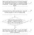
- FIG. 10 is a flow chart of a specific principle of bandwidth adjustment of an initial monopole antenna provided by the present invention.
- Fig. 11 is a schematic structural diagram of a monopole antenna bandwidth adjustment system provided by the present invention.
- the core of the present invention is to provide a monopole antenna bandwidth adjustment method and system, which realizes the advance prediction of the monopole antenna monopole antenna bandwidth and resonance characteristics, improves the antenna bandwidth optimization performance, and reduces the bandwidth adjustment period;
- the problem of radiation resistance which cannot be quantitatively analyzed, further improves the optimization performance of antenna bandwidth.
- FIG. 1 is a process flowchart of a monopole antenna bandwidth adjustment method provided by the present invention. The method includes:
- the monopole antenna and its free space are previously equivalent to a bandpass filter.
- the bandpass filter includes an LC circuit and a virtual impedance transformation network connected to the LC circuit.
- the resonance impedance of the LC circuit and the resonance of the monopole antenna Equal impedance
- FIG. 2 is an equivalent schematic diagram of a monopole antenna provided by the present invention.
- the hollow circle represents the input end of the band pass filter
- the solid circle represents the output end of the band pass filter.
- the input impedance and output impedance of the band-pass filter are 50 ⁇ .
- the monopole antenna and its free space are equivalent to a bandpass filter, where the monopole antenna can be specifically equivalent to an LC circuit (this application considers that the radiation resistance of the monopole antenna is small, so it can Ignore the radiation resistance), the input impedance of the LC circuit is used as the input impedance of the band-pass filter; the free space where the monopole antenna is located can be equivalent to the impedance port, and then the impedance of the impedance port is transformed by the virtual impedance transformation network. The transformed impedance is used as the output impedance of the band-pass filter, and the transformed impedance meets the system requirements through impedance transformation.
- the resonance impedance of the LC circuit is equal to the resonance impedance of the monopole antenna (the resonance impedance of the monopole antenna can be predicted according to it), thereby realizing the resonance and resonance type of the bandpass filter and the resonance properties of the monopole antenna the same.
- the virtual impedance transformation network can be set to be ideal and lossless, and the radiation efficiency of the monopole antenna can be set to 100%. (This is different from the traditional analysis of the radiation characteristics of the antenna and its free space equivalent to a two-port device.
- the present invention does not analyze the antenna radiation characteristics, and sets the ideal radiation, that is, the radiation efficiency is 100%.), that is, there is no radiation to the free space. Energy loss.
- S2 Separate the preset antenna matching circuit from the band pass filter, and determine the antenna impedance curve of the preset antenna matching circuit on the Smith chart;
- the preset antenna matching circuit is separated from the bandpass filter.
- the function of the antenna matching circuit is to match the impedance of the monopole antenna so that the impedance of the matched monopole antenna meets the system Requirements (for example, close to 50 ⁇ ); after obtaining the preset antenna matching circuit, the antenna impedance curve of the preset matching circuit on the smith diagram and the bandwidth (ie impedance bandwidth) curve of the preset matching circuit (bandwidth curve and smith There is a corresponding relationship between the antenna impedance curves on the figure).
- the initial antenna matching circuit can be adjusted according to the corresponding antenna impedance curve to make the monopole antenna meet the preset antenna bandwidth requirement.
- the bandpass filter when used for bandwidth analysis, other elements in the bandpass filter except the antenna matching circuit can be adjusted to maximize the bandwidth of the bandpass filter.
- the antenna matching circuit is the core of the monopole antenna bandwidth analysis, because in the monopole antenna design, the antenna matching circuit can be initially preset according to the characteristics of the monopole antenna. This initial antenna matching circuit connects the actual antenna design with the bandpass
- the bridge of filter bandwidth analysis can predict the bandwidth and resonance characteristics of the monopole antenna according to the bandwidth of the band pass filter, thereby increasing the space for optimization of the monopole antenna bandwidth.
- the preset antenna matching circuit all refers to an L-shaped network structure, that is, a series-parallel matching structure composed of two components. It is not difficult to obtain that multiple preset antenna matching circuits with different structures can be separated from the band pass filter.
- S3 Obtain the initial antenna matching circuit of the initial monopole antenna, and determine whether the initial antenna matching circuit matches the preset antenna matching circuit, if yes, go to S4;
- the initial antenna matching circuit can be predetermined according to the characteristics of the initial monopole antenna, and then the initial antenna matching circuit and the preset antenna matching circuit
- the matching here means that the components and the connection relationship of the two components are the same.
- the initial antenna matching circuit and the preset antenna matching circuit both include capacitors and inductors, and the capacitors and inductors are both connected in series.
- the initial monopole antenna is adjusted according to the antenna impedance curve of the matched preset antenna matching circuit on the Smith chart.
- the adjustment can be, for example, changing the monopole.
- the shape and/or length and/or width of the antenna are specifically determined according to actual conditions, so that the final initial monopole antenna meets the preset antenna bandwidth requirement (specifically, it may be 2402MHz-2480MHz). It is not difficult to obtain that once the preset antenna matching circuit matches the initial antenna matching circuit, the bandwidth corresponding to the preset antenna matching circuit can be obtained, and the bandwidth of the initial monopole antenna (in the antenna impedance curve) can be obtained in advance.
- the monopole antenna bandwidth adjustment method realizes the advance prediction of the monopole antenna bandwidth and resonance characteristics, improves the optimization performance of the antenna bandwidth, and reduces the bandwidth adjustment period; it also avoids the inability to quantitatively analyze the radiation resistance. The trouble of factors further improves the optimization performance of the antenna bandwidth.
- the monopole antenna and its free space are previously equivalent to a bandpass filter, including:
- the free space where the monopole antenna is located is equivalent to the impedance port of the first value, so that the monopole antenna and the free space form a two-port network, the input end impedance of the two-port network is the second value, and the output end impedance is the first value;
- the monopole antenna is equivalent to an LC circuit, so that the LC circuit and the virtual impedance transformation network form a band-pass filter, where the resonance impedance of the LC circuit is equal to the resonance impedance of the antenna.
- the free space where the monopole antenna is located is equivalent to the impedance port, and the impedance of the impedance port is the first value
- the monopole antenna and the free space where it is located form a two-port network.
- the first value of the impedance of the free space equivalent impedance port is a certain value, it may not match the impedance of other systems (that is, systems that work with bandpass filters), such as 50 ⁇ systems. Therefore, pass
- the virtual impedance transformation network converts the impedance of the impedance port from the first value to the second value to meet the impedance matching of other systems.
- the monopole antenna is equivalent to an LC circuit, where the resonant impedance of the LC circuit is equal to the resonant impedance of the antenna, and the LC circuit and the virtual impedance transformation network form a band-pass filter.
- the band-pass filter can achieve resonance and the type of resonance is the same as that of the monopole antenna, and the bandwidth of the band-pass filter is comparable to that of the monopole antenna, which is convenient for subsequent use. Bandwidth adjustment of monopole antenna.
- the first value is 377 ⁇ ; the second value is 50 ⁇ .
- the free space is equivalent to an impedance port of 377 ⁇ , and 377 ⁇ becomes 50 ⁇ after being transformed by a virtual impedance transformation network.
- 377 ⁇ is not compatible with the general 50 ⁇ system impedance and cannot be measured.
- the bandpass filter design usually uses a 50 ⁇ system, and the input and output are both 50 ⁇ . Therefore, adopting the solution of this application makes the analysis more convenient and simple.
- the second value here can also be other values, which are determined according to actual conditions.
- obtaining the initial antenna matching circuit of the initial monopole antenna includes:
- the initial matching of the initial monopole antenna is performed using the antenna parameters to obtain the initial antenna matching circuit.
- the initial monopole antenna When designing the initial monopole antenna, first divide the initial monopole antenna into an initial antenna matching circuit and an initial antenna.
- the initial antenna matching circuit is used for subsequent matching with the preset antenna matching circuit to obtain an antenna impedance curve, and then the shape and/or length and/or width of the initial antenna can be adjusted according to the antenna impedance curve.
- the antenna parameters of the initial monopole antenna need to be obtained. Therefore, the antenna parameters can be obtained by data simulation and single-port measurement. Specifically, the antenna parameter here may be the self-reflection coefficient S11 parameter (input return loss) or VSWR (Voltage Standing Wave Ratio, voltage standing wave ratio) or impedance. These three parameters can be converted to each other. After the antenna parameters are obtained, the initial antenna matching circuit of the initial monopole antenna can be determined.
- S11 parameter input return loss
- VSWR Voltage Standing Wave Ratio, voltage standing wave ratio
- the preset antenna matching circuit includes a first preset antenna matching circuit and/or a second preset antenna matching circuit and/or a third preset antenna matching circuit;
- the first preset antenna matching circuit includes a first capacitor and a first inductor, the first end of the first capacitor serves as the input end of the first preset antenna matching circuit, the second end of the first capacitor and the first end of the first inductor The connected and connected common terminal serves as the output terminal of the first preset antenna matching circuit, and the second terminal of the first inductor is grounded;
- the second preset antenna matching circuit includes a second capacitor and a third capacitor.
- the first end of the second capacitor is connected to the first end of the third capacitor and the common end of the connection is used as the input end of the second preset antenna matching circuit.
- the second end of the two capacitors is grounded, and the second end of the third capacitor is connected as the output end of the second preset antenna matching circuit;
- the third preset antenna matching circuit includes a fourth capacitor and a second inductor, and the first end of the fourth capacitor is connected to the first end of the second inductor and the common end of the connection serves as the input end of the third preset antenna matching circuit.
- the second end of the two inductors is grounded, and the second end of the fourth capacitor is used as the output end of the third preset antenna matching circuit.
- Figure 3 is a schematic diagram of a separate antenna matching circuit provided by the present invention.
- Figure 4 is a schematic diagram of another separated antenna matching circuit improved by the present invention.
- Figure 5 is a schematic diagram of another separated antenna matching circuit provided by the present invention.
- a schematic diagram of a separate first antenna matching circuit FIG. 6 is a schematic diagram of a separate second antenna matching circuit provided by the present invention
- FIG. 7 is a schematic diagram of a separate third antenna matching circuit provided by the present invention, Among them, the left half of Fig. 5-7 is the antenna matching circuit separated from the corresponding band-pass filter circuit combination.
- the band-pass filter component units (series resonant unit 102 and parallel resonant unit 101 respectively) are reorganized to form a series resonant unit 102 as the main component.
- the first band-pass filter circuit combination and the second band-pass filter circuit combination based on the parallel resonant unit 101, the first matching element K1 of the preset antenna matching circuit in the first band-pass filter circuit combination forms a virtual equivalent element Series resonance circuit 103.
- the first matching element K1 is an inductor
- the second matching element K2 of the antenna matching circuit may be a capacitor or an inductor. Therefore, the first band-pass filter circuit combination can separate two preset antenna matching circuits (corresponding to FIG. 5 and FIG. 6 respectively), and the two preset antenna matching circuits have the same bandwidth.
- the first matching element K1 of the antenna matching circuit can be an inductor or a capacitor
- the second element of the antenna matching can also be an inductor or an inductor
- Series inductance is not commonly used, mainly because if the value of the series inductance is relatively large, the inductance loss is relatively large, if the value of the series is small, it can be simplified and equivalent to 0 ⁇ . Therefore, this application only considers the case where the second matching element K2 is a capacitor, but the two preset antenna matching circuits actually separated by the second band-pass filter circuit combination also have the same bandwidth.
- FIG. 8 is a bandwidth characteristic diagram of a first band-pass filter circuit combination and a second band-pass filter circuit combination provided by the present invention.
- the bandwidth characteristics of the first band-pass filter circuit combination and the second band-pass filter circuit combination are shown in curves 105 and 106. It should be noted that the first band-pass filter circuit combination separates the bandwidth characteristic curve of the preset antenna matching circuit. As shown in curve 105, the bandwidth characteristic curve of the preset antenna matching circuit separated by the second band-pass filter circuit combination is also shown in curve 106. In this comparison of bandwidth characteristics, all capacitors have a value of 1pF, and all inductances have a value of 4.7nH. In the figure, the graph where the curve 105 is located is the bandwidth response curve of the first band-pass filter circuit combination, and the graph where the curve 106 is located is the bandwidth response curve of the second band-pass filter circuit combination.
- the black solid line represents the energy transmission from the input to the output of the filter
- the gray curve represents the return loss of the input and output, which is the curve of the antenna impedance bandwidth.
- the combination of the first band-pass filter circuit is approximately 1 times wider than the combination of the second band-pass filter circuit.
- the resonant circuit 103 included in the first band-pass filter circuit combination is series resonance
- the resonant circuit 104 included in the second band-pass filter circuit combination is parallel resonance, which is consistent with the monopole antenna usually designed as a series resonant antenna.
- FIG. 9 is a smith diagram of the pre-antenna matching circuit provided by the present invention.
- the first preset antenna matching circuit corresponds to the antenna impedance curve 11
- the second preset antenna matching circuit corresponds to the antenna impedance curve 33.
- the three preset antenna matching circuits correspond to the antenna impedance curve 22.
- the antenna impedance curve of the initial antenna matching circuit in the smith diagram and the antenna impedance curve of the preset antenna matching circuit in the smith diagram are Similarly, therefore, using the antenna impedance curve of the preset antenna matching circuit in the Smith chart to adjust the initial monopole antenna can make the initial monopole antenna meet the preset antenna bandwidth requirement.
- the straight line in the middle of the figure and the outer circle form two planes, and the two intersection points.
- the two planes are the inductive area of the upper half plane and the capacitance of the lower half plane.
- Sexual area For example, curve 11 has capacitive impedance characteristics, and 22 and 33 have inductive impedance characteristics.
- the two intersection points are 0 and ⁇ , which represent impedances of 0 and infinity, respectively.
- the monopole antenna travels clockwise from the position of infinite impedance along the capacitive area for a certain length, such as reaching the position of curve 11, such as moving on, crossing the solid line in the middle, and reaching the position of curve 22 and position 33, here ,
- the curve 11 does not cross the middle solid line, and the electrical length of the antenna is slightly less than a quarter wavelength.
- the curves 22 and 33 cross the middle solid line once, that is, they have the characteristics of greater than one-quarter wavelength and less than one-half wavelength.
- the preset antenna matching circuit includes a first preset antenna matching circuit, a second preset antenna matching circuit, and a third preset antenna matching circuit;
- S11 Determine whether the initial antenna matching circuit matches the antenna matching circuit in the preset antenna matching circuit, if yes, go to S12, otherwise, go to S14;
- S13 Determine whether the S11 parameter of the adjusted initial monopole antenna meets the preset antenna bandwidth requirement, if yes, go to S18, otherwise, go to S14;
- S14 Determine an antenna matching circuit from the remaining two antenna matching circuits in the preset antenna matching circuit, and adjust the initial monopole antenna according to the determined antenna impedance curve of the preset antenna matching circuit on the Smith chart;
- S15 Determine whether the S11 parameter of the adjusted initial monopole antenna meets the preset antenna bandwidth requirement, if yes, go to S18, otherwise, go to S16;
- S17 Determine whether the S11 parameter of the adjusted initial monopole antenna meets the preset antenna bandwidth requirement, if yes, go to S18;
- FIG. 10 is a flowchart of a specific principle of bandwidth adjustment of an initial monopole antenna provided by the present invention.
- the initial antenna matching circuit when matching the initial antenna matching circuit with the preset antenna matching circuit, first determine whether there is a preset antenna matching circuit that directly matches the initial antenna matching circuit. Matching means that the components and the connection relationship of the components are the same. If yes, adjust the initial monopole antenna according to the antenna impedance curve of the preset antenna matching circuit on the smith diagram, and obtain the adjusted initial monopole The S11 parameter of the antenna, and then judge whether the S11 parameter of the adjusted initial monopole antenna meets the preset antenna bandwidth requirement.
- the adjusted antenna will be used as the final monopole antenna; otherwise, continue from the remaining pre-
- a preset antenna matching circuit is determined in the antenna matching circuit, and the above process of adjusting the initial monopole antenna according to the antenna impedance curve of the preset antenna matching circuit on the Smith chart is repeated. If there is a preset antenna matching circuit, The adjusted S11 parameters of the initial monopole antenna meet the preset antenna bandwidth requirements, and the adjusted antenna will be determined to be the final monopole antenna. If there is no preset antenna matching circuit, the adjusted S11 parameters of the initial monopole antenna To meet the preset antenna bandwidth requirements, the monopole antenna design needs to be updated.
- multiple preset antenna matching circuits are selected to match the initial antenna matching circuit, and the preset antenna matching circuit that directly matches the initial antenna matching circuit is preferred.
- the antenna impedance curve on the smith diagram is used to perform the initial monopole antenna. The adjustment improves the matching efficiency and success rate of the initial antenna matching circuit.
- adjusting the initial monopole antenna includes:
- step S16 when the remaining two antenna matching circuits are the first preset antenna matching circuit and the second preset antenna matching circuit, select the remaining antenna matching circuit from the preset antenna matching circuit.
- One of the two antenna matching circuits is determined, including:
- an antenna matching circuit is determined from the remaining two antenna matching circuits in the preset antenna matching circuit, include:
- the first preset antenna matching circuit and the third preset antenna matching circuit have parallel inductances, so they have an ESD anti-static protection function
- the second preset antenna matching circuit includes two capacitors, which has a relatively high ESD protection capability. Poor.
- a preset antenna matching circuit or a third preset antenna matching circuit reduces the cost of the monopole antenna and reduces the volume of the monopole antenna.
- FIG. 11 is a schematic structural diagram of a monopole antenna bandwidth adjustment system provided by the present invention.
- the present invention also provides a monopole antenna bandwidth adjustment system, including:
- the equivalent unit 1 is used to pre-equivalent the monopole antenna and its free space as a bandpass filter.
- the bandpass filter includes an LC circuit and a virtual impedance transformation network connected to the LC circuit.
- the resonance impedance of the LC circuit is The resonant impedances of monopole antennas are equal;
- the antenna impedance curve determining unit 2 is used to separate the preset antenna matching circuit from the band-pass filter, and determine the antenna impedance curve of the preset antenna matching circuit on the Smith chart;
- the matching unit 3 is used to obtain the initial antenna matching circuit of the initial monopole antenna, and determine whether the initial antenna matching circuit matches the preset antenna matching circuit, and if so, trigger the broadband adjustment unit 4;
- the bandwidth adjustment unit 4 is configured to adjust the initial monopole antenna according to the antenna impedance curve of the matched preset antenna matching circuit on the Smith diagram, so that the initial monopole antenna meets the preset antenna bandwidth requirement.
Landscapes
- Details Of Aerials (AREA)
- Input Circuits Of Receivers And Coupling Of Receivers And Audio Equipment (AREA)
Abstract
本发明公开了一种单极天线带宽调整方法及系统,包括将单极天线及其所在的自由空间等效为带通滤波器,且由于LC电路的谐振阻抗与单极天线的谐振阻抗相等,则带通滤波器可以实现谐振并且谐振的类型与单极天线的谐振性质相同,因此,带通滤波器的带宽与单极天线的带宽具有可比性,基于此,可以得到预设天线匹配电路在smith图上的天线阻抗曲线,后续在初始单极天线单极天线的初始天线匹配电路与预设天线匹配电路匹配时,便可以根据匹配的预设天线匹配电路在smith图上的天线阻抗曲线对初始单极天线进行调整,从而实现了单极天线的带宽及谐振特性的提前预测,提高了天线带宽的优化性能,减少了带宽调节周期;还避免了辐射电阻这一无法定量分析因素的困扰。
Description
本申请要求于2019年8月16日提交中国专利局、申请号为201910758767.3、发明名称为“一种单极天线带宽调整方法及系统”的中国专利申请的优先权,其全部内容通过引用结合在本申请中。
本发明涉及天线带宽调节技术领域,特别是涉及一种单极天线带宽调整方法及系统。
蓝牙耳机由于其便利性而受到用户的喜爱。蓝牙耳机的外观丰富多样,蓝牙天线的设计也相应地变化,以便与蓝牙耳机的外观相适应。蓝牙耳机通常为单极天线,为了保证单极天线的性能,要求单极天线的带宽满足天线带宽要求(2402MHz-2480MHz)。现有技术中在进行单极天线带宽调整时只能根据工程师经验来进行调整,然后通过对调整后的单极天线的带宽进行检测,并根据检测后的带宽再对单极天线进行调整,并重复上述过程,直至单极天线的带宽满足天线带宽要求,该种调节方式的调节周期较长,且天线带宽的优化性能较低。
发明内容
本发明的目的是提供一种单极天线带宽调整方法及系统,实现了单极天线的带宽及谐振特性的提前预测,提高了天线带宽的优化性能,减少了带宽调节周期;还避免了辐射电阻这一无法定量分析因素的困扰,进一步提高了天线带宽的优化性能。
为解决上述技术问题,本发明提供了一种单极天线带宽调整方法,包括:
预先将单极天线及其所在的自由空间等效为带通滤波器,所述带通滤波器包括LC电路及与所述LC电路连接的虚拟阻抗变换网络,所述LC电路的谐振阻抗与所述单极天线的谐振阻抗相等;
从所述带通滤波器中分离出预设天线匹配电路,并确定所述预设天线匹配电路在smith图上的天线阻抗曲线;
获取初始单极天线的初始天线匹配电路,并判断所述初始天线匹配电路是否与所述预设天线匹配电路匹配;
如果是,则根据匹配的预设天线匹配电路在smith图上的天线阻抗曲线对所述初始单极天线进行调整,以便所述初始单极天线满足预设天线带宽要求。
优选地,所述预先将单极天线及其所在的自由空间等效为带通滤波器,包括:
将单极天线所在的自由空间等效为第一数值的阻抗端口,以便所述单极天线和所述自由空间构成双端口网络,所述双端口网络的输入端阻抗为第二数值,输出端阻抗为所述第一数值;
通过与所述单极天线连接的无损耗的虚拟阻抗变换网络将所述输出端阻抗转换为所述第二数值;
将所述单极天线等效为LC电路,以便所述LC电路和所述虚拟阻抗变换网络构成带通滤波器,其中,所述LC电路的谐振阻抗等于所述天线的谐振阻抗。
优选地,所述第一数值为377Ω;所述第二数值为50Ω。
优选地,所述获取初始单极天线的初始天线匹配电路,包括:
对初始单极天线进行单端口测量,得到天线参数;
利用所述天线参数对所述初始单极天线进行初始匹配,得到初始天线匹配电路。
优选地,所述天线参数包括自反射系数S11参数或者电压驻波比VSWR或者阻抗。
优选地,所述预设天线匹配电路包括第一预设天线匹配电路和/或第二预设天线匹配电路和/或第三预设天线匹配电路;
所述第一预设天线匹配电路包括第一电容和第一电感,所述第一电容的第一端作为所述第一预设天线匹配电路的输入端,所述第一电容的第二端与所述第一电感的第一端连接且连接的公共端作为所述第一预设天线匹配电路的输出端,所述第一电感的第二端接地;
所述第二预设天线匹配电路包括第二电容和第三电容,所述第二电容的第一端与所述第三电容的第一端连接且连接的公共端作为所述第二预设天线匹配电路的输入端,所述第二电容的第二端接地,所述第三电容的第二端连接作为所述第二预设天线匹配电路的输出端;
所述第三预设天线匹配电路包括第四电容和第二电感,所述第四电容的第一端与所述第二电感的第一端连接且连接的公共端作为所述第三预设天线匹配电路的输入端,所述第二电感的第二端接地,所述第四电容的第二端作为所述第三预设天线匹配电路的输出端。
优选地,所述预设天线匹配电路包括第一预设天线匹配电路、第二预设天线匹配电路和第三预设天线匹配电路;
所述判断所述初始天线匹配电路是否与所述预设天线匹配电路匹配,以便所述初始单极天线满足预设天线带宽要求,如果是,则根据匹配的预设天线匹配电路在smith图上的天线阻抗曲线对所述初始单极天线进行调整,以便所述初始单极天线满足预设天线带宽要求,包括:
S11:判断所述初始天线匹配电路是否与所述预设天线匹配电路中的天线匹配电路匹配,如果是,进入S12,否则,进入S14;
S12:根据匹配的预设天线匹配电路在smith图上的天线阻抗曲线对所述初始单极天线进行调整;
S13:判断调整后的初始单极天线的S11参数是否满足预设天线带宽要求,如果是,进入S18,否则,进入S14;
S14:从所述预设天线匹配电路中的剩下的两个天线匹配电路中确定一个天线匹配电路,并根据确定的预设天线匹配电路在smith图上的天线阻抗曲线对所述初始单极天线进行调整;
S15:判断调整后的初始单极天线的S11参数是否满足预设天线带宽要求,如果是,进入S18,否则,进入S16;
S16:根据所述预设天线匹配电路中剩下的最后一个天线匹配电路在smith图上的天线阻抗曲线对所述初始单极天线进行调整;
S17:判断调整后的初始单极天线的S11参数是否满足预设天线带宽要求,如果是,进入S18;
S18:确定调整后的天线为最终的单极天线。
优选地,所述对所述初始单极天线进行调整,包括:
调整所述初始单极天线的形状和/或长度和/或宽度。
优选地,步骤S16中,当所述剩下的两个天线匹配电路为第一预设天线匹配电路和第二预设天线匹配电路时,所述从所述预设天线匹配电路中的剩下的两个天线匹配电路中确定一个天线匹配电路,包括:
确定所述第一预设天线匹配电路;或者,
当所述剩下的两个天线匹配电路为第二预设天线匹配电路和第三预设天线匹配电路时,所述从所述预设天线匹配电路中的剩下的两个天线匹配电路中确定一个天线匹配电路,包括:
确定第三预设天线匹配电路。
为解决上述技术问题,本发明还提供了一种单极天线带宽调整系统,包括:
等效单元,用于预先将单极天线及其所在的自由空间等效为带通滤波器,所述带通滤波器包括LC电路及与所述LC电路连接的虚拟阻抗变换网络,所述LC电路的谐振阻抗与所述单极天线的谐振阻抗相等;
天线阻抗曲线确定单元,用于从所述带通滤波器中分离出预设天线匹配电路,并确定所述预设天线匹配电路在smith图上的天线阻抗曲线;
匹配单元,用于获取初始单极天线的初始天线匹配电路,并判断所述初始天线匹配电路是否与所述预设天线匹配电路匹配,如果是,则触发宽带调整单元;
所述带宽调整单元,用于根据匹配的预设天线匹配电路在smith图上的天线阻抗曲线对所述初始单极天线进行调整,以便所述初始单极天线满足预设天线带宽要求。
本发明提供了一种单极天线带宽调整方法,该方法包括将单极天线及其所在的自由空间等效为带通滤波器,且由于LC电路的谐振阻抗与单极天线的谐振阻抗相等,则带通滤波器可以实现谐振并且谐振的类型与单极天线的谐振性质相同,因此,带通滤波器的带宽与单极天线的带宽具有可比性,基于此,可以得到预设天线匹配电路在smith图上的天线阻抗曲线,后续在初始单极天线单极天线的初始天线匹配电路与预设天线匹配电路匹配时,便可以根据匹配的预设天线匹配电路在smith图上的天线阻抗曲线对初始单极天 线进行调整,最终初始单极天线满足预设天线带宽要求,从而实现了单极天线单极天线的带宽及谐振特性的提前预测,提高了天线带宽的优化性能,减少了带宽调节周期;还避免了辐射电阻这一无法定量分析因素的困扰,进一步提高了天线带宽的优化性能。
本发明还提供了一种单极天线带宽调整系统,具有与上述单极天线带宽调整方法相同的有益效果。
为了更清楚地说明本发明实施例中的技术方案,下面将对现有技术和实施例中所需要使用的附图作简单地介绍,显而易见地,下面描述中的附图仅仅是本发明的一些实施例,对于本领域普通技术人员来讲,在不付出创造性劳动的前提下,还可以根据这些附图获得其他的附图。
图1为本发明提供的一种单极天线带宽调整方法的过程流程图;
图2为本发明提供的一种单极天线的等效原理图;
图3为本发明提供的一种分离天线匹配电路的原理图;
图4为本发明提高的另一种分离天线匹配电路的原理图;
图5为本发明提供的一种分离第一天线匹配电路的原理图;
图6为本发明提供的一种分离第二天线匹配电路的原理图;
图7为本发明提供的一种分离第三天线匹配电路的原理图;
图8为本发明提供的一种第一带通滤波电路组合和第二带通滤波电路组合的带宽特性图;
图9为本发明提供的预先天线匹配电路的smith图;
图10为本发明提供的一种具体地初始单极天线的带宽调整原理流程图;
图11为本发明提供的一种单极天线带宽调整系统的结构示意图。
本发明的核心是提供一种单极天线带宽调整方法及系统,实现了单极天线单极天线的带宽及谐振特性的提前预测,提高了天线带宽的优化性能,减少了带宽调节周期;还避免了辐射电阻这一无法定量分析因素的困扰,进一步提高了天线带宽的优化性能。
为使本发明实施例的目的、技术方案和优点更加清楚,下面将结合本发明实施例中的附图,对本发明实施例中的技术方案进行清楚、完整地描述,显然,所描述的实施例是本发明一部分实施例,而不是全部的实施例。基于本发明中的实施例,本领域普通技术人员在没有做出创造性劳动前提下所获得的所有其他实施例,都属于本发明保护的范围。
请参照图1,图1为本发明提供的一种单极天线带宽调整方法的过程流程图,该方法包括:
S1:预先将单极天线及其所在的自由空间等效为带通滤波器,带通滤波器包括LC电路及与LC电路连接的虚拟阻抗变换网络,LC电路的谐振阻抗与单极天线的谐振阻抗相等;
本申请考虑到带通滤波器可以实现谐振且谐振的类型与单极天线的谐振性质相同,因此,带通滤波器的带宽(本申请中提及的带宽指的是相对带宽)与单极天线的带宽具有可比性。基于此,本申请将单极天线这一单端口器件等效为双端口器件。请参照图2,图2为本发明提供的一种单极天线的等效原理图,图中,空心圈表示带通滤波器输入端,实心圈代表带通滤波器输出端,图2中以带通滤波器的输入阻抗和输出阻抗为50Ω为例。具体地,将单极天线及其所在的自由空间等效为带通滤波器,其中,单极天线可以具体等效为LC电路(本申请考虑到单极天线的辐射电阻很小,因此,可以将辐射电阻忽略不计),LC电路的输入阻抗作为带通滤波器的输入阻抗;单极天线所在的自由空间可以等效为阻抗端口,再通过虚拟阻抗变换网络将阻抗端口的阻抗进行阻抗变换,变换后的阻抗作为带通滤波器的输出阻抗,通过阻抗变换从而实现变换后的阻抗满足系统要求。此外,LC电路的谐振阻抗与单极天线的谐振阻抗(单极天线的谐振阻抗根据是可以预知的)相等,从而实现了带通滤波器可以实现谐振且谐振的类型与单极天线的谐振性质相同。
另外,为了避免带通滤波器及单极天线的带宽分析的对比性变差,在实际应用中,可以设定虚拟阻抗变换网络是理想无损耗的,同时设定单极天线的辐射效率100%(这和传统将天线及其所在自由空间等效为两端口器件分析辐射特性不一样,本发明不分析天线辐射特性,设定理想辐射,即辐射效率100%。),即向自由空间辐射无能量损耗。
S2:从带通滤波器中分离出预设天线匹配电路,并确定预设天线匹配电路在smith图上的天线阻抗曲线;
在得到带通滤波器后,从带通滤波器中分离出预设天线匹配电路,其中,天线匹配电路的作用是为了与单极天线的阻抗配合,使得配合后的单极天线的阻抗满足系统要求(例如接近50Ω);在得到预设天线匹配电路后,便可以得到预设匹配电路在smith图上的天线阻抗曲线以及预设匹配电路的带宽(也即阻抗带宽)曲线(带宽曲线与smith图上的天线阻抗曲线之间存在对应关系),后续在应用过程中,初始天线匹配电路便可以根据相应地天线阻抗曲线进行调整,以便使单极天线满足预设天线带宽要求。
具体地,在利用带通滤波器进行带宽分析时,除天线匹配电路外的带通滤波器中的其他元件均可调整,使得带通滤波器的带宽最大。分离出天线匹配电路是单极天线带宽分析的核心,因为在单极天线设计中,天线匹配电路可以根据单极天线的特点进行初始预设,此初始天线匹配电路是连接实际天线设计与带通滤波器带宽分析的桥梁,后续根据带通滤波器的带宽便可预测单极天线的带宽及谐振特性,从而提升了单极天线带宽优化的空间。
此外,还需要说明的是,本申请中,预设天线匹配电路均指的是L型网络结构,即两个元器件构成的串并联匹配结构。不难得到,带通滤波器中可以分离出多个不同结构的预设天线匹配电路。
S3:获取初始单极天线的初始天线匹配电路,并判断初始天线匹配电路是否与预设天线匹配电路匹配,如果是,进入S4;
在实际应用中,在进行初始单极天线(也即待设计单极天线)设计时,可以根据初始单极天线的特点预先确定初始天线匹配电路,然后将初始天线匹配电路与预设天线匹配电路进行匹配,这里的匹配指的是两者的元器件及元器件的连接关系相同,例如,初始天线匹配电路和预设天线匹配电路均包括电容和电感,且电容和电感均为串联。
S4:根据匹配的预设天线匹配电路在smith图上的天线阻抗曲线对初始单极天线进行调整,以便初始单极天线满足预设天线带宽要求。
在存在预设天线匹配电路与初始天线匹配电路匹配时,则根据该匹配的预设天线匹配电路在smith图上的天线阻抗曲线对初始单极天线进行调整,这里的调整例如可以为改变单极天线的形状和/或长度和/或宽度等,具体根据 实际情况来定,以使得最终初始单极天线满足预设天线带宽要求(具体可以为2402MHz-2480MHz)。不难得到,一旦存在预设天线匹配电路与初始天线匹配电路匹配,则便可以得到预设天线匹配电路对应的带宽,进而也便可以预先得到该初始单极天线的带宽(在天线阻抗曲线中可以得到),后续根据天线阻抗曲线对初始单极天线进行调整便可。可见,本申请提供的单极天线带宽调整方法实现了单极天线的带宽及谐振特性的提前预测,提高了天线带宽的优化性能,减少了带宽调节周期;还避免了辐射电阻这一无法定量分析因素的困扰,进一步提高了天线带宽的优化性能。
在上述实施例的基础上:
作为一种优选地实施例,预先将单极天线及其所在的自由空间等效为带通滤波器,包括:
将单极天线所在的自由空间等效为第一数值的阻抗端口,以便单极天线和自由空间构成双端口网络,双端口网络的输入端阻抗为第二数值,输出端阻抗为第一数值;
通过与单极天线连接的无损耗的虚拟阻抗变换网络将输出端阻抗转换为第二数值;
将单极天线等效为LC电路,以便LC电路和虚拟阻抗变换网络构成带通滤波器,其中,LC电路的谐振阻抗等于天线的谐振阻抗。
具体地,首先将单极天线所在的自由空间等效为阻抗端口,阻抗端口的阻抗为第一数值,则单极天线及其所在的自由空间便构成了双端口网络。又考虑到自由空间等效的阻抗端口的阻抗的第一数值是一定值,其与其他系统(也即与带通滤波器配合工作的系统)例如50Ω系统的阻抗可能不匹配,因此,再通过虚拟阻抗变换网络将阻抗端口的阻抗由第一数值转换为第二数值,以满足其他系统的阻抗匹配。再将单极天线等效为LC电路,其中,LC电路的谐振阻抗等于天线的谐振阻抗,则LC电路和虚拟阻抗变换网络构成带通滤波器。通过该种方式,使得带通滤波器可以实现谐振并且谐振的类型与单极天线的谐振性质相同,进而使得带通滤波器的带宽与单极天线的带宽具有可比性,便于后续使用过程中的单极天线的带宽调整。
作为一种优选地实施例,第一数值为377Ω;第二数值为50Ω。
具体地,本申请将自由空间等效为377Ω的阻抗端口,且377Ω经过虚拟阻抗变换网络变换后变成50Ω,主要是考虑到377Ω无法兼容通用的50Ω系统阻抗,无法进行实际测量。其次,带通滤波器设计通常使用50Ω系统,输入输出均采用50Ω,因此,采用采用本申请的方案使得分析更方便,简单。
当然,这里的第二数值还可以为其他数值,根据实际情况来定。
作为一种优选地实施例,获取初始单极天线的初始天线匹配电路,包括:
对初始单极天线进行单端口测量,得到天线参数;
利用天线参数对初始单极天线进行初始匹配,得到初始天线匹配电路。
在对初始单极天线进行设计时,先将初始单极天线分为初始天线匹配电路和初始天线。初始天线匹配电路用来后续与预设天线匹配电路进行匹配,以得到天线阻抗曲线,进而便可以根据天线阻抗曲线对初始天线的形状和/或长度和/或宽度等参数进行调整。
为了得到初始天线匹配电路,需要先得到初始单极天线的天线参数,因此,先对其进行数据仿真并进行单端口测量,便可得到天线参数。具体地,这里的天线参数可以为自反射系数S11参数(输入回波损耗)或者VSWR(Voltage Standing Wave Ratio,电压驻波比)或者阻抗。这三个参数可以相互换算,在得到天线参数后,便可以确定初始单极天线的初始天线匹配电路。
作为一种优选地实施例,预设天线匹配电路包括第一预设天线匹配电路和/或第二预设天线匹配电路和/或第三预设天线匹配电路;
第一预设天线匹配电路包括第一电容和第一电感,第一电容的第一端作为第一预设天线匹配电路的输入端,第一电容的第二端与第一电感的第一端连接且连接的公共端作为第一预设天线匹配电路的输出端,第一电感的第二端接地;
第二预设天线匹配电路包括第二电容和第三电容,第二电容的第一端与第三电容的第一端连接且连接的公共端作为第二预设天线匹配电路的输入端,第二电容的第二端接地,第三电容的第二端连接作为第二预设天线匹配电路的输出端;
第三预设天线匹配电路包括第四电容和第二电感,第四电容的第一端与第二电感的第一端连接且连接的公共端作为第三预设天线匹配电路的输入 端,第二电感的第二端接地,第四电容的第二端作为第三预设天线匹配电路的输出端。
请参照图3-图7,图3为本发明提供的一种分离天线匹配电路的原理图,图4为本发明提高的另一种分离天线匹配电路的原理图,图5为本发明提供的一种分离第一天线匹配电路的原理图,图6为本发明提供的一种分离第二天线匹配电路的原理图,图7为本发明提供的一种分离第三天线匹配电路的原理图,其中,图5-7中的左半部分均为各自对应的带通滤波电路组合分离出的天线匹配电路。
下面给出本申请确定预设天线匹配电路的过程,具体地,先将带通滤波器组成单元(分别为串联谐振单元102和并联谐振单元101)进行重组,形成以串联谐振单元102为主的第一带通滤波电路组合和以并联谐振单元101为主的第二带通滤波电路组合,第一带通滤波电路组合中的预设天线匹配电路的第一匹配元件K1与虚拟等效元件形成串联谐振电路103。结合实际天线匹配电路中第一匹配元件K1为电感的情况非常少,因为电感越大,电感带来的损耗越大,故本申请讨论第一匹配电源为电容的情况。根据滤波电路组合,天线匹配电路的第二匹配元件K2可以是电容或者电感。故第一带通滤波电路组合可以分离出两种预设天线匹配电路(分别对应图5和图6),且该两种预设天线匹配电路具有相同带宽。
对于第二带通滤波电路组合,天线匹配电路的第一匹配元件K1可以是电感,也可以是电容,天线匹配的第二元件也可以是电感或者电感,但由于第二匹配元件K2是串联,串联电感不常用,主要是因为串联的电感的值如果比较大的话,电感损耗比较大,如果串联的值较小的话,可以简化等效为0Ω。因此,本申请只考虑第二匹配元件K2为电容的情况,但第二带通滤波电路组合实际上分离出的两种预设天线匹配电路也具有相同的带宽。
还需要注意的是,这里的相同带宽指的是两种预设天线匹配电路的元件数值不变的情况下,仅是连接关系如两种预设天线匹配电路图所示。
请参照图8,图8为本发明提供的一种第一带通滤波电路组合和第二带通滤波电路组合的带宽特性图。
第一带通滤波电路组合和第二带通滤波电路组合的带宽特性如曲线105,106所示,需要说明的是,第一带通滤波电路组合分离出预设天线匹配电路 的带宽特性曲线也如曲线105所示,第二带通滤波电路组合分离出预设天线匹配电路的带宽特性曲线也如曲线106所示。该带宽特性比较中,所有电容均取值1pF,所有电感均取值4.7nH。图中曲线105所在的图面为第一带通滤波电路组合的带宽响应曲线,106所在的图面为第二带通滤波电路组合的带宽响应曲线。黑色实心线代表滤波器输入到输出的能量传输,灰色曲线代表输入和输出的回波损耗,也就是天线阻抗带宽的曲线。以-10dB为基准线,第一带通滤波电路组合比第二带通滤波电路组合宽接近1倍。进一步分析,第一带通滤波电路组合包含的谐振电路103为串联谐振,而第二带通滤波电路组合包含的谐振电路104为并联谐振,这与单极天线通常设计为串联谐振天线相吻合。当然,也有少量天线设计为并联天线,前提是满足天线阻抗带宽的情况下。如今,在双无线耳机越来越小的尺寸趋势下,通过本发明的分析方法可知,在带宽不足的情况下,需要尽量避免天线为并联谐振。进一步地,请参照图9,图9为本发明提供的预先天线匹配电路的smith图,第一预设天线匹配电路对应天线阻抗曲线11,第二预设天线匹配电路对应天线阻抗曲线33,第三预设天线匹配电路对应天线阻抗曲线22。在实际应用中,若初始天线匹配电路与某一预设天线匹配电路匹配,则该初始天线匹配电路在smith图中的天线阻抗曲线与该预设天线匹配电路在smith图中的天线阻抗曲线是类似的,因此,利用该预设天线匹配电路在smith图中的天线阻抗曲线对初始单极天线进行调整,能够使得初始单极天线满足预设天线带宽要求。
需要说明的是,在smith图中,如图中间直线与外圈圆形成两个平面,两个交点,两个平面分别是上半平面具有电感性质的感性区域和下半平面具有电容性质的容性区域。如11曲线具有电容阻抗特性,22和33具有电感阻抗特性。两个交点分别是0和∞,分别代表阻抗为0和无穷大。
感兴趣频段的天线的谐振情况:
如图所示,单极天线从阻抗无穷大的位置沿容性区域顺时针行进一定长度,比如到达曲线11位置,如继续前进,跨越中间的实线,可到达曲线22位置,以及33位置,这里,曲线11未跨过中间实线,及天线电长度略小于四分之一波长。曲线22和33跨越一次中间实线,即具有大于四分之一波长,而小于二分之一波长的特点。
作为一种优选地实施例,预设天线匹配电路包括第一预设天线匹配电路、第二预设天线匹配电路和第三预设天线匹配电路;
判断初始天线匹配电路是否与预设天线匹配电路匹配,以便初始单极天线满足预设天线带宽要求,如果是,则根据匹配的预设天线匹配电路在smith图上的天线阻抗曲线对初始单极天线进行调整,以便初始单极天线满足预设天线带宽要求,包括:
S11:判断初始天线匹配电路是否与预设天线匹配电路中的天线匹配电路匹配,如果是,进入S12,否则,进入S14;
S12:根据匹配的预设天线匹配电路在smith图上的天线阻抗曲线对初始单极天线进行调整;
S13:判断调整后的初始单极天线的S11参数是否满足预设天线带宽要求,如果是,进入S18,否则,进入S14;
S14:从预设天线匹配电路中的剩下的两个天线匹配电路中确定一个天线匹配电路,并根据确定的预设天线匹配电路在smith图上的天线阻抗曲线对初始单极天线进行调整;
S15:判断调整后的初始单极天线的S11参数是否满足预设天线带宽要求,如果是,进入S18,否则,进入S16;
S16:根据预设天线匹配电路中剩下的最后一个天线匹配电路在smith图上的天线阻抗曲线对初始单极天线进行调整;
S17:判断调整后的初始单极天线的S11参数是否满足预设天线带宽要求,如果是,进入S18;
S18:确定调整后的天线为最终的单极天线。
请参照图10,图10为本发明提供的一种具体地初始单极天线的带宽调整原理流程图。
具体地,由于预设天线匹配电路为多个,则在进行初始天线匹配电路与预设天线匹配电路匹配时,首先判断是否有与初始天线匹配电路直接匹配的预设天线匹配电路,这里的直接匹配指的是元器件构成以及元器件的连接关系相同,如果有,则根据该预设天线匹配电路在smith图上的天线阻抗曲线对初始单极天线进行调整,并获取调整后的初始单极天线的S11参数,然后判断调整后的初始单极天线的S11参数是否满足预设天线带宽要求,如果是, 则将调整后的天线作为最终的单极天线,否则,则继续从剩下的预设天线匹配电路中确定一个预设天线匹配电路,并重复上述根据预设天线匹配电路在smith图上的天线阻抗曲线对初始单极天线进行调整的过程,如果存在某一预设天线匹配电路使得调整后的初始单极天线的S11参数满足预设天线带宽要求,则将确定调整后的天线为最终的单极天线,如果不存在预设天线匹配电路使得调整后的初始单极天线的S11参数满足预设天线带宽要求,则需要更新单极天线设计。
可见,选用多个预设天线匹配电路与初始天线匹配电路去进行匹配,且优先选用与初始天线匹配电路直接匹配的预设天线匹配电路在smith图上的天线阻抗曲线去对初始单极天线进行调整,提高了初始天线匹配电路的匹配效率和成功率。
作为一种优选地实施例,对初始单极天线进行调整,包括:
调整初始单极天线的形状和/或长度和/或宽度。
作为一种优选地实施例,步骤S16中,当剩下的两个天线匹配电路为第一预设天线匹配电路和第二预设天线匹配电路时,从预设天线匹配电路中的剩下的两个天线匹配电路中确定一个天线匹配电路,包括:
确定第一预设天线匹配电路;或者,
当剩下的两个天线匹配电路为第二预设天线匹配电路和第三预设天线匹配电路时,从预设天线匹配电路中的剩下的两个天线匹配电路中确定一个天线匹配电路,包括:
确定第三预设天线匹配电路。
具体地,第一预设天线匹配电路和第三预设天线匹配电路均有并电感,因此,其具有ESD防静电保护作用,而第二预设天线匹配电路包括两个电容,ESD防护能力较差,在实际应用中可能需要增加TVS管等防护措施,提高了单极天线的成本,增大了单极天线的体积,而采用本申请提供的方案,优选选取自带ESD防静电功能的第一预设天线匹配电路或第三预设天线匹配电路,降低了单极天线的成本,减小了单极天线的体积。
请参照图11,图11为本发明提供的一种单极天线带宽调整系统的结构示意图,本发明还提供了一种单极天线带宽调整系统,包括:
等效单元1,用于预先将单极天线及其所在的自由空间等效为带通滤波器,带通滤波器包括LC电路及与LC电路连接的虚拟阻抗变换网络,LC电路的谐振阻抗与单极天线的谐振阻抗相等;
天线阻抗曲线确定单元2,用于从带通滤波器中分离出预设天线匹配电路,并确定预设天线匹配电路在smith图上的天线阻抗曲线;
匹配单元3,用于获取初始单极天线的初始天线匹配电路,并判断初始天线匹配电路是否与预设天线匹配电路匹配,如果是,则触发宽带调整单元4;
带宽调整单元4,用于根据匹配的预设天线匹配电路在smith图上的天线阻抗曲线对初始单极天线进行调整,以便初始单极天线满足预设天线带宽要求。
对于本发明提供的单极天线带宽调整系统的介绍请参照上述方法实施例,本发明在此不再赘述。
需要说明的是,在本说明书中,诸如第一和第二等之类的关系术语仅仅用来将一个实体或者操作与另一个实体或操作区分开来,而不一定要求或者暗示这些实体或操作之间存在任何这种实际的关系或者顺序。而且,术语“包括”、“包含”或者其任何其他变体意在涵盖非排他性的包含,从而使得包括一系列要素的过程、方法、物品或者设备不仅包括那些要素,而且还包括没有明确列出的其他要素,或者是还包括为这种过程、方法、物品或者设备所固有的要素。在没有更多限制的情况下,由语句“包括一个……”限定的要素,并不排除在包括所述要素的过程、方法、物品或者设备中还存在另外的相同要素。
对所公开的实施例的上述说明,使本领域专业技术人员能够实现或使用本发明。对这些实施例的多种修改对本领域的专业技术人员来说将是显而易见的,本文中所定义的一般原理可以在不脱离本发明的精神或范围的情况下,在其他实施例中实现。因此,本发明将不会被限制于本文所示的这些实施例,而是要符合与本文所公开的原理和新颖特点相一致的最宽的范围。
Claims (10)
- 一种单极天线带宽调整方法,其特征在于,包括:预先将单极天线及其所在的自由空间等效为带通滤波器,所述带通滤波器包括LC电路及与所述LC电路连接的虚拟阻抗变换网络,所述LC电路的谐振阻抗与所述单极天线的谐振阻抗相等;从所述带通滤波器中分离出预设天线匹配电路,并确定所述预设天线匹配电路在smith图上的天线阻抗曲线;获取初始单极天线的初始天线匹配电路,并判断所述初始天线匹配电路是否与所述预设天线匹配电路匹配;如果是,则根据匹配的预设天线匹配电路在smith图上的天线阻抗曲线对所述初始单极天线进行调整,以便所述初始单极天线满足预设天线带宽要求。
- 如权利要求1所述的单极天线带宽调整方法,其特征在于,所述预先将单极天线及其所在的自由空间等效为带通滤波器,包括:将单极天线所在的自由空间等效为第一数值的阻抗端口,以便所述单极天线和所述自由空间构成双端口网络,所述双端口网络的输入端阻抗为第二数值,输出端阻抗为所述第一数值;通过与所述单极天线连接的无损耗的虚拟阻抗变换网络将所述输出端阻抗转换为所述第二数值;将所述单极天线等效为LC电路,以便所述LC电路和所述虚拟阻抗变换网络构成带通滤波器,其中,所述LC电路的谐振阻抗等于所述天线的谐振阻抗。
- 如权利要求2所述的单极天线带宽调整方法,其特征在于,所述第一数值为377Ω;所述第二数值为50Ω。
- 如权利要求1所述的单极天线带宽调整方法,其特征在于,所述获取初始单极天线的初始天线匹配电路,包括:对初始单极天线进行单端口测量,得到天线参数;利用所述天线参数对所述初始单极天线进行初始匹配,得到初始天线匹配电路。
- 如权利要求4所述的单极天线带宽调整方法,其特征在于,所述天线参数包括自反射系数S11参数或者电压驻波比VSWR或者阻抗。
- 如权利要求1至5任一项所述的单极天线带宽调整方法,其特征在于,所述预设天线匹配电路包括第一预设天线匹配电路和/或第二预设天线匹配电路和/或第三预设天线匹配电路;所述第一预设天线匹配电路包括第一电容和第一电感,所述第一电容的第一端作为所述第一预设天线匹配电路的输入端,所述第一电容的第二端与所述第一电感的第一端连接且连接的公共端作为所述第一预设天线匹配电路的输出端,所述第一电感的第二端接地;所述第二预设天线匹配电路包括第二电容和第三电容,所述第二电容的第一端与所述第三电容的第一端连接且连接的公共端作为所述第二预设天线匹配电路的输入端,所述第二电容的第二端接地,所述第三电容的第二端连接作为所述第二预设天线匹配电路的输出端;所述第三预设天线匹配电路包括第四电容和第二电感,所述第四电容的第一端与所述第二电感的第一端连接且连接的公共端作为所述第三预设天线匹配电路的输入端,所述第二电感的第二端接地,所述第四电容的第二端作为所述第三预设天线匹配电路的输出端。
- 如权利要求6所述的单极天线带宽调整方法,其特征在于,所述预设天线匹配电路包括第一预设天线匹配电路、第二预设天线匹配电路和第三预设天线匹配电路;所述判断所述初始天线匹配电路是否与所述预设天线匹配电路匹配,以便所述初始单极天线满足预设天线带宽要求,如果是,则根据匹配的预设天线匹配电路在smith图上的天线阻抗曲线对所述初始单极天线进行调整,以便所述初始单极天线满足预设天线带宽要求,包括:S11:判断所述初始天线匹配电路是否与所述预设天线匹配电路中的天线匹配电路匹配,如果是,进入S12,否则,进入S14;S12:根据匹配的预设天线匹配电路在smith图上的天线阻抗曲线对所述初始单极天线进行调整;S13:判断调整后的初始单极天线的S11参数是否满足预设天线带宽要求,如果是,进入S18,否则,进入S14;S14:从所述预设天线匹配电路中的剩下的两个天线匹配电路中确定一个天线匹配电路,并根据确定的预设天线匹配电路在smith图上的天线阻抗曲线对所述初始单极天线进行调整;S15:判断调整后的初始单极天线的S11参数是否满足预设天线带宽要求,如果是,进入S18,否则,进入S16;S16:根据所述预设天线匹配电路中剩下的最后一个天线匹配电路在smith图上的天线阻抗曲线对所述初始单极天线进行调整;S17:判断调整后的初始单极天线的S11参数是否满足预设天线带宽要求,如果是,进入S18;S18:确定调整后的天线为最终的单极天线。
- 如权利要求7所述的单极天线带宽调整方法,其特征在于,所述对所述初始单极天线进行调整,包括:调整所述初始单极天线的形状和/或长度和/或宽度。
- 如权利要求7所述的单极天线带宽调整方法,其特征在于,步骤S16中,当所述剩下的两个天线匹配电路为第一预设天线匹配电路和第二预设天线匹配电路时,所述从所述预设天线匹配电路中的剩下的两个天线匹配电路中确定一个天线匹配电路,包括:确定所述第一预设天线匹配电路;或者,当所述剩下的两个天线匹配电路为第二预设天线匹配电路和第三预设天线匹配电路时,从所述预设天线匹配电路中的剩下的两个天线匹配电路中确定一个天线匹配电路,包括:确定第三预设天线匹配电路。
- 一种单极天线带宽调整系统,其特征在于,包括:等效单元,用于预先将单极天线及其所在的自由空间等效为带通滤波器,所述带通滤波器包括LC电路及与所述LC电路连接的虚拟阻抗变换网络,所述LC电路的谐振阻抗与所述单极天线的谐振阻抗相等;天线阻抗曲线确定单元,用于从所述带通滤波器中分离出预设天线匹配电路,并确定所述预设天线匹配电路在smith图上的天线阻抗曲线;匹配单元,用于获取初始单极天线的初始天线匹配电路,并判断所述初始天线匹配电路是否与所述预设天线匹配电路匹配,如果是,则触发宽带调整单元;所述带宽调整单元,用于根据匹配的预设天线匹配电路在smith图上的天线阻抗曲线对所述初始单极天线进行调整,以便所述初始单极天线满足预设天线带宽要求。
Applications Claiming Priority (2)
| Application Number | Priority Date | Filing Date | Title |
|---|---|---|---|
| CN201910758767.3 | 2019-08-16 | ||
| CN201910758767.3A CN110444893B (zh) | 2019-08-16 | 2019-08-16 | 一种单极天线带宽调整方法及系统 |
Publications (1)
| Publication Number | Publication Date |
|---|---|
| WO2021031293A1 true WO2021031293A1 (zh) | 2021-02-25 |
Family
ID=68436157
Family Applications (1)
| Application Number | Title | Priority Date | Filing Date |
|---|---|---|---|
| PCT/CN2019/108245 Ceased WO2021031293A1 (zh) | 2019-08-16 | 2019-09-26 | 一种单极天线带宽调整方法及系统 |
Country Status (2)
| Country | Link |
|---|---|
| CN (1) | CN110444893B (zh) |
| WO (1) | WO2021031293A1 (zh) |
Families Citing this family (2)
| Publication number | Priority date | Publication date | Assignee | Title |
|---|---|---|---|---|
| CN111475990B (zh) * | 2020-03-20 | 2023-09-05 | 歌尔科技有限公司 | 一种单极天线的设计方法、装置及系统 |
| CN114498039B (zh) * | 2021-12-18 | 2022-12-02 | 中国电波传播研究所(中国电子科技集团公司第二十二研究所) | 一种提高单极天线匹配效果的双端匹配方法 |
Citations (13)
| Publication number | Priority date | Publication date | Assignee | Title |
|---|---|---|---|---|
| CN1523774A (zh) * | 2003-02-17 | 2004-08-25 | 明基电通股份有限公司 | 一种天线阻抗匹配电路的设计方法 |
| JP2005129985A (ja) * | 2003-10-21 | 2005-05-19 | Hitachi Kokusai Electric Inc | 自動インピーダンス整合方法 |
| CN101147294A (zh) * | 2005-04-15 | 2008-03-19 | 诺基亚公司 | 具有多个谐振频率的天线 |
| CN101740855A (zh) * | 2010-01-28 | 2010-06-16 | 福建三元达软件有限公司 | 天线的协同设计及安装方法 |
| CN102075158A (zh) * | 2010-12-29 | 2011-05-25 | 重庆邮电大学 | 一种超宽带阻抗匹配网络设计方法 |
| US8019307B2 (en) * | 2007-12-05 | 2011-09-13 | Winstron Neweb Corporation | Method and related electronic device for adjustment of a radio frequency circuit by impedance loading features |
| CN103473427A (zh) * | 2013-09-24 | 2013-12-25 | 上海无线电设备研究所 | 一种应用于标签天线设计的复阻抗匹配方法 |
| CN104485900A (zh) * | 2014-11-27 | 2015-04-01 | 重庆蓝岸通讯技术有限公司 | 基于功率放大器关键指标数据的天线阻抗匹配方法 |
| CN104538749A (zh) * | 2014-12-30 | 2015-04-22 | 深圳市共进电子股份有限公司 | 外置天线及其阻抗匹配网络参数的调试方法、天线 |
| CN106650087A (zh) * | 2016-12-20 | 2017-05-10 | 西安航天华迅科技有限公司 | 一种l型阻抗匹配网络设计方法 |
| CN108711668A (zh) * | 2018-04-25 | 2018-10-26 | 歌尔股份有限公司 | 天线装置及电子设备 |
| CN109586735A (zh) * | 2018-11-12 | 2019-04-05 | 维沃移动通信有限公司 | 阻抗匹配电路、收发装置及收发设备 |
| CN110085995A (zh) * | 2019-04-18 | 2019-08-02 | 西安星网天线技术有限公司 | 一种自动调谐短波环天线及其调谐方法 |
Family Cites Families (23)
| Publication number | Priority date | Publication date | Assignee | Title |
|---|---|---|---|---|
| CN101501991B (zh) * | 2006-06-27 | 2012-06-13 | 传感电子公司 | 带有动态阻抗匹配的谐振电路调谐系统 |
| US7683851B2 (en) * | 2007-03-19 | 2010-03-23 | Broadcom Corporation | Method and system for using a single transformer for FM transmit and FM receive functions |
| JP5081742B2 (ja) * | 2007-06-29 | 2012-11-28 | 日本電波工業株式会社 | アンテナ分波器 |
| CN102257615A (zh) * | 2008-12-21 | 2011-11-23 | 莱尔德技术股份有限公司 | 供与便携式通信设备一起使用的天线组件 |
| CN102694585A (zh) * | 2012-05-25 | 2012-09-26 | 中国电子科技集团公司第十研究所 | 自适应调整天线组阵时延差的校正方法 |
| CN103579755B (zh) * | 2012-08-07 | 2016-06-01 | 联想(北京)有限公司 | 天线和用于形成天线的方法 |
| US9799952B2 (en) * | 2013-07-02 | 2017-10-24 | Wispry, Inc. | Filtering antenna systems, devices, and methods |
| CN103594803A (zh) * | 2013-10-28 | 2014-02-19 | 瑞声精密制造科技(常州)有限公司 | 自可配置谐振天线及其工作方法 |
| US9172410B2 (en) * | 2014-01-15 | 2015-10-27 | Mediatek Inc. | Transmitter having integrated design of multiple wireless communication modules |
| US9762274B2 (en) * | 2014-05-29 | 2017-09-12 | Qualcomm Incorporated | Feedback receive path with RF filter |
| US10333494B2 (en) * | 2014-12-24 | 2019-06-25 | Qorvo Us, Inc. | Simplified acoustic RF resonator parallel capacitance compensation |
| US11036294B2 (en) * | 2015-10-07 | 2021-06-15 | The Governing Council Of The University Of Toronto | Wireless power and data transmission system for wearable and implantable devices |
| KR101697356B1 (ko) * | 2016-02-02 | 2017-01-18 | 광운대학교 산학협력단 | 주파수 가변 범위가 확장된 광대역 재구성 안테나 구조 |
| CN105789840A (zh) * | 2016-02-25 | 2016-07-20 | 努比亚技术有限公司 | 一种滤波天线装置、天线带宽的调整方法和移动终端 |
| CN106299671B (zh) * | 2016-10-17 | 2019-05-17 | 山西大学 | 双频带滤波天线 |
| CN106329066A (zh) * | 2016-10-19 | 2017-01-11 | 深圳市信维通信股份有限公司 | 一种降低高频手机天线sar值的系统 |
| CN206098681U (zh) * | 2016-10-19 | 2017-04-12 | 深圳市信维通信股份有限公司 | 一种降低高频手机天线sar值的系统 |
| JP2019062309A (ja) * | 2017-09-25 | 2019-04-18 | 株式会社村田製作所 | 方向性結合器及び通信ユニット |
| US10741909B2 (en) * | 2017-09-26 | 2020-08-11 | Apple Inc. | Electronic devices having multi-band slot antennas |
| CN208445738U (zh) * | 2018-08-09 | 2019-01-29 | 歌尔科技有限公司 | 一种谐波失真滤除设备及终端 |
| CN109462031A (zh) * | 2018-10-10 | 2019-03-12 | 清华大学 | 基于可变电感和可变电容的双级可调谐天线 |
| CN109861696A (zh) * | 2018-12-21 | 2019-06-07 | 惠州Tcl移动通信有限公司 | 一种天线调节方法及天线系统终端 |
| CN110087159B (zh) * | 2019-04-03 | 2020-11-17 | 歌尔科技有限公司 | 一种反馈降噪方法、系统、耳机及存储介质 |
-
2019
- 2019-08-16 CN CN201910758767.3A patent/CN110444893B/zh active Active
- 2019-09-26 WO PCT/CN2019/108245 patent/WO2021031293A1/zh not_active Ceased
Patent Citations (13)
| Publication number | Priority date | Publication date | Assignee | Title |
|---|---|---|---|---|
| CN1523774A (zh) * | 2003-02-17 | 2004-08-25 | 明基电通股份有限公司 | 一种天线阻抗匹配电路的设计方法 |
| JP2005129985A (ja) * | 2003-10-21 | 2005-05-19 | Hitachi Kokusai Electric Inc | 自動インピーダンス整合方法 |
| CN101147294A (zh) * | 2005-04-15 | 2008-03-19 | 诺基亚公司 | 具有多个谐振频率的天线 |
| US8019307B2 (en) * | 2007-12-05 | 2011-09-13 | Winstron Neweb Corporation | Method and related electronic device for adjustment of a radio frequency circuit by impedance loading features |
| CN101740855A (zh) * | 2010-01-28 | 2010-06-16 | 福建三元达软件有限公司 | 天线的协同设计及安装方法 |
| CN102075158A (zh) * | 2010-12-29 | 2011-05-25 | 重庆邮电大学 | 一种超宽带阻抗匹配网络设计方法 |
| CN103473427A (zh) * | 2013-09-24 | 2013-12-25 | 上海无线电设备研究所 | 一种应用于标签天线设计的复阻抗匹配方法 |
| CN104485900A (zh) * | 2014-11-27 | 2015-04-01 | 重庆蓝岸通讯技术有限公司 | 基于功率放大器关键指标数据的天线阻抗匹配方法 |
| CN104538749A (zh) * | 2014-12-30 | 2015-04-22 | 深圳市共进电子股份有限公司 | 外置天线及其阻抗匹配网络参数的调试方法、天线 |
| CN106650087A (zh) * | 2016-12-20 | 2017-05-10 | 西安航天华迅科技有限公司 | 一种l型阻抗匹配网络设计方法 |
| CN108711668A (zh) * | 2018-04-25 | 2018-10-26 | 歌尔股份有限公司 | 天线装置及电子设备 |
| CN109586735A (zh) * | 2018-11-12 | 2019-04-05 | 维沃移动通信有限公司 | 阻抗匹配电路、收发装置及收发设备 |
| CN110085995A (zh) * | 2019-04-18 | 2019-08-02 | 西安星网天线技术有限公司 | 一种自动调谐短波环天线及其调谐方法 |
Also Published As
| Publication number | Publication date |
|---|---|
| CN110444893B (zh) | 2020-05-26 |
| CN110444893A (zh) | 2019-11-12 |
Similar Documents
| Publication | Publication Date | Title |
|---|---|---|
| CN108493551B (zh) | 一种ipd超宽频带功分器 | |
| CN104811156B (zh) | 一种用于谐振增强型宽带阻抗匹配电路的匹配方法 | |
| CN106233531A (zh) | 具有可调去耦结构的mimo天线 | |
| CN103490794A (zh) | 可变天调匹配网络结构电路 | |
| TWI594589B (zh) | 射頻匹配電路及無線通訊裝置 | |
| CN107707215A (zh) | 一种宽带负群时延微波电路及其设计方法 | |
| WO2021031293A1 (zh) | 一种单极天线带宽调整方法及系统 | |
| CN110739135B (zh) | 一种基于电感可调的变压器 | |
| CN101569095A (zh) | 双频匹配电路 | |
| CN105958664B (zh) | 一种基于最大功率匹配的无线电能传输系统功率效率优化方法 | |
| CN113224492B (zh) | 一种基于互感耦合的超宽带功分器芯片 | |
| CN103594767B (zh) | 一种集成化腔体滤波器 | |
| CN105428764A (zh) | 一种宽带大功率螺旋滤波器 | |
| Suvarna et al. | Transformer-based tunable matching network design techniques in 40-nm CMOS | |
| JP2017204997A (ja) | 電界結合型電力供給システム用フィルタ | |
| CN219459025U (zh) | 滤波器 | |
| CN202905948U (zh) | 一种复合左右手传输线器件及天线 | |
| CN114900149B (zh) | 一种低通滤波器及光通信测试装置 | |
| CN101569098A (zh) | 双频匹配电路 | |
| CN113675597B (zh) | 一种附加匹配网络结构参数确定方法 | |
| CN111384908B (zh) | 功分器电路、功分器及功分器电路的设计方法 | |
| CN103199821A (zh) | 一种超宽带双调谐变压器实现方法 | |
| CN111475990B (zh) | 一种单极天线的设计方法、装置及系统 | |
| WO2023098918A1 (zh) | 一种极零点跟踪的二阶可调lc陷波滤波器 | |
| CN101558561A (zh) | 双频匹配电路 |
Legal Events
| Date | Code | Title | Description |
|---|---|---|---|
| 121 | Ep: the epo has been informed by wipo that ep was designated in this application |
Ref document number: 19941876 Country of ref document: EP Kind code of ref document: A1 |
|
| NENP | Non-entry into the national phase |
Ref country code: DE |
|
| 122 | Ep: pct application non-entry in european phase |
Ref document number: 19941876 Country of ref document: EP Kind code of ref document: A1 |