WO2021024916A1 - Dispositif semi-conducteur au carbure de silicium - Google Patents
Dispositif semi-conducteur au carbure de silicium Download PDFInfo
- Publication number
- WO2021024916A1 WO2021024916A1 PCT/JP2020/029300 JP2020029300W WO2021024916A1 WO 2021024916 A1 WO2021024916 A1 WO 2021024916A1 JP 2020029300 W JP2020029300 W JP 2020029300W WO 2021024916 A1 WO2021024916 A1 WO 2021024916A1
- Authority
- WO
- WIPO (PCT)
- Prior art keywords
- side wall
- insulating film
- region
- semiconductor layer
- silicon carbide
- Prior art date
Links
- 239000004065 semiconductor Substances 0.000 title claims abstract description 132
- HBMJWWWQQXIZIP-UHFFFAOYSA-N silicon carbide Chemical compound [Si+]#[C-] HBMJWWWQQXIZIP-UHFFFAOYSA-N 0.000 title claims abstract description 74
- 229910010271 silicon carbide Inorganic materials 0.000 title claims abstract description 74
- 239000000758 substrate Substances 0.000 claims abstract description 40
- 229910052799 carbon Inorganic materials 0.000 claims description 27
- 125000004432 carbon atom Chemical group C* 0.000 claims 4
- 239000010410 layer Substances 0.000 description 121
- XUIMIQQOPSSXEZ-UHFFFAOYSA-N Silicon Chemical compound [Si] XUIMIQQOPSSXEZ-UHFFFAOYSA-N 0.000 description 29
- 229910052710 silicon Inorganic materials 0.000 description 29
- 239000010703 silicon Substances 0.000 description 29
- 238000004519 manufacturing process Methods 0.000 description 27
- 150000001721 carbon Chemical group 0.000 description 20
- 238000005530 etching Methods 0.000 description 15
- 230000015556 catabolic process Effects 0.000 description 14
- 239000013078 crystal Substances 0.000 description 13
- VYPSYNLAJGMNEJ-UHFFFAOYSA-N Silicium dioxide Chemical compound O=[Si]=O VYPSYNLAJGMNEJ-UHFFFAOYSA-N 0.000 description 12
- 230000005684 electric field Effects 0.000 description 10
- 238000010438 heat treatment Methods 0.000 description 9
- 239000007789 gas Substances 0.000 description 8
- 239000011229 interlayer Substances 0.000 description 7
- 238000005468 ion implantation Methods 0.000 description 7
- 230000001590 oxidative effect Effects 0.000 description 7
- 229910052814 silicon oxide Inorganic materials 0.000 description 6
- IJGRMHOSHXDMSA-UHFFFAOYSA-N Atomic nitrogen Chemical compound N#N IJGRMHOSHXDMSA-UHFFFAOYSA-N 0.000 description 5
- 101000726148 Homo sapiens Protein crumbs homolog 1 Proteins 0.000 description 5
- 101000726110 Homo sapiens Protein crumbs homolog 2 Proteins 0.000 description 5
- 102100027331 Protein crumbs homolog 1 Human genes 0.000 description 5
- 102100027317 Protein crumbs homolog 2 Human genes 0.000 description 5
- KZBUYRJDOAKODT-UHFFFAOYSA-N Chlorine Chemical compound ClCl KZBUYRJDOAKODT-UHFFFAOYSA-N 0.000 description 4
- 238000005229 chemical vapour deposition Methods 0.000 description 4
- 239000012141 concentrate Substances 0.000 description 4
- 239000012535 impurity Substances 0.000 description 4
- 238000000034 method Methods 0.000 description 4
- 238000001020 plasma etching Methods 0.000 description 4
- OKTJSMMVPCPJKN-UHFFFAOYSA-N Carbon Chemical compound [C] OKTJSMMVPCPJKN-UHFFFAOYSA-N 0.000 description 3
- 101000726113 Homo sapiens Protein crumbs homolog 3 Proteins 0.000 description 3
- 102100027316 Protein crumbs homolog 3 Human genes 0.000 description 3
- 239000012159 carrier gas Substances 0.000 description 3
- 239000000460 chlorine Substances 0.000 description 3
- 230000003647 oxidation Effects 0.000 description 3
- 238000007254 oxidation reaction Methods 0.000 description 3
- 230000001681 protective effect Effects 0.000 description 3
- 239000012495 reaction gas Substances 0.000 description 3
- 235000012239 silicon dioxide Nutrition 0.000 description 3
- 239000000377 silicon dioxide Substances 0.000 description 3
- XKRFYHLGVUSROY-UHFFFAOYSA-N Argon Chemical compound [Ar] XKRFYHLGVUSROY-UHFFFAOYSA-N 0.000 description 2
- MYMOFIZGZYHOMD-UHFFFAOYSA-N Dioxygen Chemical compound O=O MYMOFIZGZYHOMD-UHFFFAOYSA-N 0.000 description 2
- OAICVXFJPJFONN-UHFFFAOYSA-N Phosphorus Chemical compound [P] OAICVXFJPJFONN-UHFFFAOYSA-N 0.000 description 2
- ATUOYWHBWRKTHZ-UHFFFAOYSA-N Propane Chemical compound CCC ATUOYWHBWRKTHZ-UHFFFAOYSA-N 0.000 description 2
- 229910052581 Si3N4 Inorganic materials 0.000 description 2
- 229910001882 dioxygen Inorganic materials 0.000 description 2
- 125000005843 halogen group Chemical group 0.000 description 2
- 229910052757 nitrogen Inorganic materials 0.000 description 2
- 229910052698 phosphorus Inorganic materials 0.000 description 2
- 239000011574 phosphorus Substances 0.000 description 2
- HQVNEWCFYHHQES-UHFFFAOYSA-N silicon nitride Chemical compound N12[Si]34N5[Si]62N3[Si]51N64 HQVNEWCFYHHQES-UHFFFAOYSA-N 0.000 description 2
- 102100029968 Calreticulin Human genes 0.000 description 1
- ZAMOUSCENKQFHK-UHFFFAOYSA-N Chlorine atom Chemical compound [Cl] ZAMOUSCENKQFHK-UHFFFAOYSA-N 0.000 description 1
- PXGOKWXKJXAPGV-UHFFFAOYSA-N Fluorine Chemical compound FF PXGOKWXKJXAPGV-UHFFFAOYSA-N 0.000 description 1
- 101000793651 Homo sapiens Calreticulin Proteins 0.000 description 1
- UFHFLCQGNIYNRP-UHFFFAOYSA-N Hydrogen Chemical compound [H][H] UFHFLCQGNIYNRP-UHFFFAOYSA-N 0.000 description 1
- 229910004298 SiO 2 Inorganic materials 0.000 description 1
- BLRPTPMANUNPDV-UHFFFAOYSA-N Silane Chemical compound [SiH4] BLRPTPMANUNPDV-UHFFFAOYSA-N 0.000 description 1
- 230000004913 activation Effects 0.000 description 1
- 229910052782 aluminium Inorganic materials 0.000 description 1
- XAGFODPZIPBFFR-UHFFFAOYSA-N aluminium Chemical compound [Al] XAGFODPZIPBFFR-UHFFFAOYSA-N 0.000 description 1
- 229910052786 argon Inorganic materials 0.000 description 1
- 125000004429 atom Chemical group 0.000 description 1
- 230000015572 biosynthetic process Effects 0.000 description 1
- 230000008859 change Effects 0.000 description 1
- 238000006243 chemical reaction Methods 0.000 description 1
- 229910052801 chlorine Inorganic materials 0.000 description 1
- 239000011248 coating agent Substances 0.000 description 1
- 238000000576 coating method Methods 0.000 description 1
- 239000004020 conductor Substances 0.000 description 1
- 230000000694 effects Effects 0.000 description 1
- 230000005669 field effect Effects 0.000 description 1
- 229910052731 fluorine Inorganic materials 0.000 description 1
- 239000011737 fluorine Substances 0.000 description 1
- 239000011521 glass Substances 0.000 description 1
- 230000012447 hatching Effects 0.000 description 1
- 239000001307 helium Substances 0.000 description 1
- 229910052734 helium Inorganic materials 0.000 description 1
- SWQJXJOGLNCZEY-UHFFFAOYSA-N helium atom Chemical compound [He] SWQJXJOGLNCZEY-UHFFFAOYSA-N 0.000 description 1
- 230000006872 improvement Effects 0.000 description 1
- 230000001939 inductive effect Effects 0.000 description 1
- 239000011261 inert gas Substances 0.000 description 1
- 229910044991 metal oxide Inorganic materials 0.000 description 1
- 150000004706 metal oxides Chemical class 0.000 description 1
- 230000004048 modification Effects 0.000 description 1
- 238000012986 modification Methods 0.000 description 1
- 239000005360 phosphosilicate glass Substances 0.000 description 1
- 238000005498 polishing Methods 0.000 description 1
- 229910021420 polycrystalline silicon Inorganic materials 0.000 description 1
- 229920005591 polysilicon Polymers 0.000 description 1
- 239000001294 propane Substances 0.000 description 1
- 239000002994 raw material Substances 0.000 description 1
- 229910000077 silane Inorganic materials 0.000 description 1
- 239000000126 substance Substances 0.000 description 1
- 230000003746 surface roughness Effects 0.000 description 1
Images


Classifications
-
- H—ELECTRICITY
- H01—ELECTRIC ELEMENTS
- H01L—SEMICONDUCTOR DEVICES NOT COVERED BY CLASS H10
- H01L29/00—Semiconductor devices specially adapted for rectifying, amplifying, oscillating or switching and having potential barriers; Capacitors or resistors having potential barriers, e.g. a PN-junction depletion layer or carrier concentration layer; Details of semiconductor bodies or of electrodes thereof ; Multistep manufacturing processes therefor
- H01L29/02—Semiconductor bodies ; Multistep manufacturing processes therefor
- H01L29/12—Semiconductor bodies ; Multistep manufacturing processes therefor characterised by the materials of which they are formed
-
- H—ELECTRICITY
- H01—ELECTRIC ELEMENTS
- H01L—SEMICONDUCTOR DEVICES NOT COVERED BY CLASS H10
- H01L29/00—Semiconductor devices specially adapted for rectifying, amplifying, oscillating or switching and having potential barriers; Capacitors or resistors having potential barriers, e.g. a PN-junction depletion layer or carrier concentration layer; Details of semiconductor bodies or of electrodes thereof ; Multistep manufacturing processes therefor
- H01L29/66—Types of semiconductor device ; Multistep manufacturing processes therefor
- H01L29/68—Types of semiconductor device ; Multistep manufacturing processes therefor controllable by only the electric current supplied, or only the electric potential applied, to an electrode which does not carry the current to be rectified, amplified or switched
- H01L29/70—Bipolar devices
- H01L29/72—Transistor-type devices, i.e. able to continuously respond to applied control signals
- H01L29/739—Transistor-type devices, i.e. able to continuously respond to applied control signals controlled by field-effect, e.g. bipolar static induction transistors [BSIT]
-
- H—ELECTRICITY
- H01—ELECTRIC ELEMENTS
- H01L—SEMICONDUCTOR DEVICES NOT COVERED BY CLASS H10
- H01L29/00—Semiconductor devices specially adapted for rectifying, amplifying, oscillating or switching and having potential barriers; Capacitors or resistors having potential barriers, e.g. a PN-junction depletion layer or carrier concentration layer; Details of semiconductor bodies or of electrodes thereof ; Multistep manufacturing processes therefor
- H01L29/66—Types of semiconductor device ; Multistep manufacturing processes therefor
- H01L29/68—Types of semiconductor device ; Multistep manufacturing processes therefor controllable by only the electric current supplied, or only the electric potential applied, to an electrode which does not carry the current to be rectified, amplified or switched
- H01L29/76—Unipolar devices, e.g. field effect transistors
- H01L29/772—Field effect transistors
- H01L29/78—Field effect transistors with field effect produced by an insulated gate
Definitions
- This disclosure relates to a silicon carbide semiconductor device.
- a trench gate type MOSFET Metal Oxide Semiconductor Field Effect Transistor in which a thick insulating film is provided at the bottom of the gate trench is disclosed (for example, Patent Document 1).
- the silicon carbide semiconductor device has a silicon carbide substrate having a main surface, a gate insulating film on the silicon carbide substrate, and a gate electrode on the gate insulating film.
- the silicon carbide substrate includes a first semiconductor layer having a first conductive type, a second semiconductor layer provided on the first semiconductor layer and having a second conductive type, and the second semiconductor layer. It has a third semiconductor layer provided above and separated from the first semiconductor layer by the second semiconductor layer and having the first conductive type.
- a trench extending in the first direction is provided on the main surface, and the trench penetrates the bottom surface formed of the first semiconductor layer, the third semiconductor layer, and the second semiconductor layer.
- the first side wall surface connected to the bottom surface is separated from the first side wall surface in a second direction perpendicular to the first direction, and penetrates the third semiconductor layer and the second semiconductor layer.
- a second side wall surface connected to the bottom surface and an end portion of the trench extending along the first direction are formed, and the bottom surface penetrates the third semiconductor layer and the second semiconductor layer. It has a third side wall surface connected to the first side wall surface and the second side wall surface connected to the second side wall surface.
- the gate insulating film includes a bottom region located on the bottom surface, a first side wall region located on the first side wall surface, and a second side wall region located on the second side wall surface.
- the thickness of the bottom region, the thickness of the third side wall region, and the thickness of the top region are all the minimum thickness of the first side wall region on the second semiconductor layer and said. It is greater than any of the minimum thicknesses of the second sidewall region on the second semiconductor layer.
- FIG. 1 is a cross-sectional view (No. 1) showing the configuration of the silicon carbide semiconductor device according to the embodiment.
- FIG. 2 is a cross-sectional view (No. 2) showing the configuration of the silicon carbide semiconductor device according to the embodiment.
- FIG. 3 is a perspective view showing a configuration of a gate insulating film in the silicon carbide semiconductor device according to the embodiment.
- FIG. 4 is a plan view showing the configuration of the gate insulating film in the silicon carbide semiconductor device according to the embodiment.
- FIG. 5 is a cross-sectional view (No. 1) showing a part of FIG. 1 in an enlarged manner.
- FIG. 6 is a cross-sectional view (No. 2) showing a part of FIG. 1 in an enlarged manner.
- FIG. 7A is a cross-sectional view (No. 1) showing a method of manufacturing the silicon carbide semiconductor device according to the embodiment.
- FIG. 7B is a cross-sectional view (No. 2) showing a method of manufacturing the silicon carbide semiconductor device according to the embodiment.
- FIG. 7C is a cross-sectional view (No. 3) showing a method of manufacturing the silicon carbide semiconductor device according to the embodiment.
- FIG. 7D is a cross-sectional view (No. 4) showing a method of manufacturing the silicon carbide semiconductor device according to the embodiment.
- FIG. 7E is a cross-sectional view (No. 5) showing a method of manufacturing the silicon carbide semiconductor device according to the embodiment.
- FIG. 7F is a cross-sectional view (No. 1) showing a method of manufacturing the silicon carbide semiconductor device according to the embodiment.
- FIG. 7G is a cross-sectional view (No. 7) showing a method of manufacturing the silicon carbide semiconductor device according to the embodiment.
- FIG. 7H is a cross-sectional view (No. 8) showing a method of manufacturing the silicon carbide semiconductor device according to the embodiment.
- FIG. 7I is a cross-sectional view (No. 9) showing a method of manufacturing the silicon carbide semiconductor device according to the embodiment.
- FIG. 7J is a cross-sectional view (No. 10) showing a method of manufacturing the silicon carbide semiconductor device according to the embodiment.
- FIG. 7K is a cross-sectional view (No. 11) showing a method of manufacturing the silicon carbide semiconductor device according to the embodiment.
- FIG. 7L is a cross-sectional view (No. 12) showing a method of manufacturing the silicon carbide semiconductor device according to the embodiment.
- FIG. 7M is a cross-sectional view (No. 13) showing a method of manufacturing the silicon carbide semiconductor device according to the embodiment.
- FIG. 8A is a cross-sectional view (No. 14) showing a method of manufacturing the silicon carbide semiconductor device according to the embodiment.
- FIG. 8B is a cross-sectional view (No. 15) showing a method of manufacturing the silicon carbide semiconductor device according to the embodiment.
- FIG. 8C is a cross-sectional view (No. 16) showing a method of manufacturing the silicon carbide semiconductor device according to the embodiment.
- FIG. 8D is a cross-sectional view (No.
- FIG. 8E is a cross-sectional view (No. 18) showing a method of manufacturing the silicon carbide semiconductor device according to the embodiment.
- FIG. 8F is a cross-sectional view (No. 19) showing a method of manufacturing the silicon carbide semiconductor device according to the embodiment.
- FIG. 8G is a cross-sectional view (No. 20) showing a method of manufacturing the silicon carbide semiconductor device according to the embodiment.
- FIG. 8H is a cross-sectional view (No. 21) showing a method of manufacturing the silicon carbide semiconductor device according to the embodiment.
- FIG. 8I is a cross-sectional view (No. 22) showing a method of manufacturing the silicon carbide semiconductor device according to the embodiment.
- FIG. 8J is a cross-sectional view (No. 23) showing a method of manufacturing the silicon carbide semiconductor device according to the embodiment.
- FIG. 8K is a cross-sectional view (No. 24) showing a method of manufacturing the silicon carbide semiconductor device according to the embodiment.
- FIG. 8L is a cross-sectional view (No. 25) showing a method of manufacturing the silicon carbide semiconductor device according to the embodiment.
- an object of the present disclosure is to provide a silicon carbide semiconductor device capable of improving dielectric breakdown resistance.
- the silicon carbide semiconductor device includes a silicon carbide substrate having a main surface, a gate insulating film on the silicon carbide substrate, and a gate electrode on the gate insulating film.
- the silicon carbide substrate includes a first semiconductor layer having a first conductive type, a second semiconductor layer provided on the first semiconductor layer and having a second conductive type, and the second semiconductor layer.
- a trench provided above, separated from the first semiconductor layer by the second semiconductor layer, has a third semiconductor layer having the first conductive type, and extends in the first direction on the main surface.
- the trench is provided with a bottom surface made of the first semiconductor layer, a first side wall surface that penetrates the third semiconductor layer and the second semiconductor layer and is connected to the bottom surface, and said.
- the gate insulating film includes a bottom region located on the bottom surface, a first side wall region located on the first side wall surface, a second side wall region located on the second side wall surface, and the above. It has a third side wall region located on the third side wall surface and a top region located on the upper surface of the third semiconductor layer and connected to the third side wall region, and has a thickness of the bottom region. Both the thickness of the third side wall region and the thickness of the top region are the minimum thickness of the first side wall region on the second semiconductor layer and the second side wall region. It is larger than any of the minimum thicknesses on the second semiconductor layer.
- a part of the second semiconductor layer functions as a channel in the vicinity of the first side wall surface and the second side wall surface.
- the electric field tends to concentrate at the corner of the bottom of the trench, but in this silicon carbide semiconductor device, the thickness of the bottom region of the gate insulating film is the first side wall region and It is larger than the minimum thickness of the second side wall region on the second semiconductor layer, that is, the thickness of the gate insulating film on the portion that functions as a channel of the second semiconductor layer. Therefore, even if the electric field is concentrated on the corner of the bottom of the trench, excellent withstand voltage can be obtained.
- the gate electrode When the gate electrode is provided in the trench, the electric field is likely to be concentrated at the corner of the upper edge of the trench, but in this silicon carbide semiconductor device, the thickness and the top region of the third side wall region of the gate insulating film.
- the thickness of the gate insulating film is larger than the thickness of the gate insulating film on the portion that functions as the channel of the second semiconductor layer. Therefore, even if the electric field is concentrated on the corner of the upper edge of the trench, excellent withstand voltage can be obtained. Therefore, the dielectric breakdown resistance can be improved.
- the third side wall region and the top region are a first insulating film that directly covers the silicon carbide substrate and a second insulating film provided on the first insulating film.
- the first insulating film has a first carbon atom concentration
- the second insulating film has a second carbon atom concentration
- the second carbon atom concentration is the first carbon atom concentration. It may be smaller than the carbon atom concentration of.
- the second insulating film may be thicker than the first insulating film. Since the second insulating film is thick, a further excellent dielectric breakdown withstand voltage can be obtained.
- the first side wall surface has a first side surface made of the first semiconductor layer, a second side surface made of a second semiconductor layer, and a third. It has a third side surface made of a semiconductor layer, and the second side wall surface has a fourth side surface made of the first semiconductor layer, a fifth side surface made of a second semiconductor layer, and a third side surface.
- the first insulating film and the second insulating film are also provided in the bottom region, the first side wall region, and the second side wall region. The first insulating film is located on the first bottom surface located on the bottom surface, the first side wall portion located on the first side wall surface, and the second side wall surface.
- the side wall portion has a first to third region located on each of the first to third side surfaces, and the second side wall portion is on each of the fourth to sixth side surfaces.
- the second insulating film has a fourth to sixth region located, and the second insulating film has a second bottom portion located on the first bottom portion and a fourth side wall located on the first side wall portion. A portion, a fifth side wall portion located on the second side wall portion, a sixth side wall portion located on the third side wall portion, and a second top portion located on the first top portion.
- the fourth side wall portion is located above the first lower end connected to the second bottom portion and any of the first and second regions, and the third region.
- the fifth side wall has a first upper end away from the second lower end connected to the second bottom and above any of the fourth and fifth regions. It has a second upper end located in and away from the sixth region, and the sixth side wall is a third lower end connected to the second bottom and the second top. It may have a third upper end connected to.
- the gate insulating film is thicker in the portion where the second insulating film is provided than in the portion where the second insulating film is not provided. Then, mainly the second bottom portion, the fourth side wall portion, and the fifth side wall portion provide excellent dielectric breakdown resistance at the corners of the bottom of the trench, and mainly the sixth side wall portion and the sixth side wall portion.
- the second top provides excellent dielectric breakdown resistance at the corners of the upper edge of the trench.
- the thickness of the second insulating film may be 100 nm or more and 300 nm or less.
- the thickness of the second insulating film is 100 nm or more, more excellent dielectric breakdown resistance can be obtained. If the thickness of the second insulating film exceeds 300 nm, the cost may become excessive.
- the second line of intersection with the upper surface of the above may be parallel to each other. Since the first line of intersection and the second line of intersection are parallel to each other, it is easy to use a surface on which excellent mobility can be obtained on both the first side wall surface and the second side wall surface.
- the third line of intersection between the third side wall surface and the upper surface of the third semiconductor layer may be arcuate. If the third line of intersection is arcuate, the electric field tends to concentrate at the corners of the upper edge of the trench, but excellent dielectric breakdown resistance can be obtained even if the electric field concentrates.
- FIG. 1 and 2 are cross-sectional views showing the configuration of the silicon carbide semiconductor device according to the embodiment.
- FIG. 3 is a perspective view showing a configuration of a gate insulating film in the silicon carbide semiconductor device according to the embodiment.
- FIG. 4 is a plan view showing the configuration of the gate insulating film in the silicon carbide semiconductor device according to the embodiment.
- 5 and 6 are cross-sectional views showing a part of FIG. 1 in an enlarged manner.
- FIG. 1 shows a cross section along the line I-I in FIGS. 2, 3 and 4.
- FIG. 2 shows a cross section along line II-II in FIGS. 1, 3 and 4.
- FIG. 5 mainly shows the components of the first insulating film
- FIG. 6 mainly shows the components of the second insulating film and the dimensions of the gate insulating film.
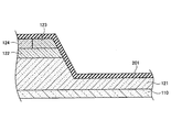
- the vertical MOSFET 501 includes an epitaxial substrate 100, a gate insulating film 200, a gate electrode 230, an interlayer insulating film 203, a source electrode 221 and a drain electrode 211. And a source wiring 222 and a protective electrode 212.
- the epitaxial substrate 100 is made of silicon carbide and has a single crystal substrate 110 and an epitaxial layer provided on the single crystal substrate 110.
- the epitaxial substrate 100 has a main surface 111 on the epitaxial layer side.
- the main surface 111 is, for example, a surface inclined at an off angle of less than 8 ° with respect to the (000-1) surface or the (000-1) surface.
- the off angle may be 6 ° or less, or 4 ° or less.
- the off angle may be 2 ° or more.
- the single crystal substrate 110 and the epitaxial layer are, for example, polytype 4H hexagonal silicon carbide.
- the single crystal substrate 110 has an n-type conductive type containing n-type impurities such as nitrogen (N).
- the epitaxial layer has an n - layer 121, a p-type body layer 122, an n region 123, and a contact region 124.
- the n - layer 121 has an n-type due to the addition of a donor. It is preferable that the donor is added to the n - layer 121 not by ion implantation but by the addition of impurities during the epitaxial growth of the n - layer 121.
- the donor concentration of the n - layer 121 is preferably lower than the donor concentration of the single crystal substrate 110.
- the donor concentration of n - layer 121 is preferably 1 ⁇ 10 15 cm -3 or more and 5 ⁇ 10 16 cm -3 or less, for example 8 ⁇ 10 15 cm -3 .
- the p-type body layer 122 is provided on the n - layer 121, and has a p-type (second conductive type) due to the addition of an acceptor.
- the acceptor concentration of the p-type body layer 122 is, for example, 1 ⁇ 10 18 cm -3 .
- the n region 123 has an n type.
- the n region 123 is provided on the p-type body layer 122 and is separated from the n - layer 121 by the p-type body layer 122.
- the contact region 124 has a p-type.
- the contact region 124 is formed on a part of the p-type body layer 122 so as to be connected to the p-type body layer 122.
- the epitaxial substrate 100 is an example of a silicon carbide substrate.
- the n - layer 121 is an example of the first semiconductor layer.
- the p-type body layer 122 is an example of a second semiconductor layer.
- the n region 123 is an example of the third semiconductor layer.
- a plurality of trench TRs are provided on the main surface 111 of the epitaxial substrate 100.
- the trench TR extends in a first direction parallel to, for example, the main surface 111, and a plurality of trench TRs are arranged in a second direction orthogonal to the main surface 111 and the first direction.
- the trench TR has a bottom surface BT composed of n - layer 121.
- the trench TR has a first side wall surface 11 that penetrates the n region 123 and the p-type body layer 122 and is connected to the bottom surface BT.
- the trench TR has a second side wall surface 12 that is separated from the first side wall surface 11 in a direction parallel to the main surface 111, penetrates the n region 123 and the p-type body layer 122, and is connected to the bottom surface BT.
- the trench TR has a third side wall surface 13 that penetrates the n region 123 and the p-type body layer 122, is connected to the bottom surface BT, and is connected to the first side wall surface 11 and the second side wall surface 12.
- the first side wall surface 11 and the second side wall surface 12 include a channel surface CH (FIG. 3) on the p-shaped body layer 122.
- the bottom surface BT is a flat surface substantially parallel to the main surface 111.
- the first side wall surface 11, the second side wall surface 12, and the third side wall surface 13 are inclined with respect to the main surface 111.
- the trench TR expands toward the opening side.
- the first side wall surface 11 and the second side wall surface 12 are preferably crystal planes having a predetermined plane orientation, for example, a crystal plane having a plane orientation (0-33-8) (special), particularly on the p-type body layer 122. Face).
- the crystal plane having a plane orientation (0-33-8) is a crystal plane from which excellent mobility can be obtained.
- the first line of intersection CL1 between the first side wall surface 11 and the upper surface 123A of the n region 123 and the second line of intersection CL3 between the second side wall surface 12 and the upper surface 123A are parallel to each other.
- a surface capable of obtaining excellent mobility on both the first side wall surface 11 and the second side wall surface 12 for example, the above-mentioned special Easy to use surface.
- the third line of intersection CL3 between the third side wall surface 13 and the upper surface 123A may be arcuate. When the third line of intersection CL3 has an arc shape, a trench TR is likely to be formed.
- the first side wall surface 11 has first to third side surfaces SW1 to SW3 including n - layer 121, p-type body layer 122, and n-region 123, respectively.
- the second side wall surface 12 has fourth to sixth side surfaces SW4 to SW6 including n - layer 121, p-type body layer 122, and n-region 123, respectively.
- the third side wall surface 13 has seventh to ninth side surfaces SW7 to SW9 including n - layer 121, p-type body layer 122, and n-region 123, respectively.
- the gate insulating film 200 is provided on the trench TR.
- the gate insulating film 200 separates the epitaxial substrate 100 and the gate electrode 230 in the trench TR.
- the gate insulating film 200 has a bottom region 300B located on the bottom surface BT, a first side wall region 301 located on the first side wall surface 11, and a second side wall surface.
- the gate insulating film 200 includes a first insulating film 201 that directly covers each of the first to third side wall surfaces 11 to 13 and the bottom surface BT, and a second insulating film 202 provided on the first insulating film 201. And have.
- Each of the first and second insulating films 201 and 202 has a first and second carbon atom concentration.
- the second carbon atom concentration may be lower than the first carbon atom concentration.
- the first carbon atom concentration may be greater than 1 ⁇ 10 15 cm -3 .
- the second carbon atom concentration may be less than 1 ⁇ 10 15 cm -3 and may be substantially zero.
- the first insulating film 201 includes a portion located on the corner portion CRB1 formed by the bottom surface BT and the first side wall surface 11, and the bottom surface BT and the second side wall surface 12. Corner portion CRT formed by a portion located on the corner portion CRB2 formed by the bottom surface BT, a portion located on the corner portion CRB3 formed by the bottom surface BT and the third side wall surface 13, and the corner portion CRT formed by the third side wall surface 13 and the upper surface 123A surface. It has a portion located above. Specifically, as shown in FIGS. 2 and 5, the first insulating film 201 has a first bottom portion 310B located on the bottom surface BT and a first side wall located on the first side wall surface 11. A portion 311, a second side wall portion 312 located on the second side wall surface 12, a third side wall portion 313 located on the third side wall surface 13, and a first top portion located on the upper surface 123A. It has 310T and.
- the first side wall portion 311 has first to third regions 411 to 413 located above each of the first to third side surfaces SW1 to SW3.
- the second side wall 312 has fourth to sixth regions 414 to 416 located above each of the fourth to sixth side surfaces SW4 to SW6.
- the third side wall portion 313 has seventh to ninth regions 417 to 419 located above each of the seventh to ninth side surfaces SW7 to SW9.
- the first insulating film 201 is preferably an oxide film, and more preferably one obtained by thermally oxidizing the surface of the trench TR of the epitaxial substrate 100.
- the second insulating film 202 has a portion located on the corner portion CRB1, a portion located on the corner portion CRB2, and a corner portion via the first insulating film 201. It has a portion located on the CRB3 and a portion located on the corner CRT.
- the second insulating film 202 has a second bottom portion 320B located on the first bottom portion 310B and a second insulating film 202 located on the first side wall portion 311.
- the fifth side wall portion 325 located on the second side wall portion 312, the sixth side wall portion 326 located on the third side wall portion 313, and the first top portion 310T. It has a second top 320T and is located.
- the fourth side wall portion 324 has a first one end E41 connected to a second bottom portion 320B and one of the first and second regions 411 and 412 (see FIG. 5). It has a first other end E42 located above and away from the third region 413.
- the fifth side wall 325 is located above either the second end E51 connected to the second bottom 320B and either the first and second regions 411,412 (see FIG. 5) and the third. It has a second other end E52 away from region 413.
- the first other end E42 and the second other end E52 may be located on the boundary between the first region 411 and the second region 412. As shown in FIG.
- the sixth side wall portion 326 has a third one end E61 connected to the second bottom 320B and a third other end E62 connected to the second top 320T.
- the second insulating film 202 may be made of at least one of silicon oxide, silicon nitride, and glass phosphosilicate.
- the second insulating film 202 may be a thermal oxide film of a film containing silicon and not carbon, and is made of, for example, silicon dioxide (SiO 2 ).
- the bottom region 300B of the gate insulating film 200 includes a first bottom 310B of the first insulating film 201 and a second bottom 320B of the second insulating film 202.
- the first side wall region 301 of the gate insulating film 200 includes a first side wall portion 311 of the first insulating film 201 and a fourth side wall portion 324 of the second insulating film 202.
- the second side wall region 302 of the gate insulating film 200 includes a second side wall portion 312 of the first insulating film 201 and a fifth side wall portion 325 of the second insulating film 202.
- the third side wall region 303 of the gate insulating film 200 includes a third side wall portion 313 of the first insulating film 201 and a sixth side wall portion 326 of the second insulating film 202.
- the top region 300T of the gate insulating film 200 includes a first top 310T of the first insulating film 201 and a second top 320T of the second insulating film 202.
- the bottom region 300B has a thickness d 0 .
- the first side wall region 301 and the second side wall region 302 have a portion having the first insulating film 201 and not having the second insulating film 202, that is, a portion composed of only the first insulating film 201. this portion has a thickness d 1.
- the first side wall region 301 and the second side wall region 302 include a portion having the first insulating film 201 and the second insulating film 202, and this portion has a thickness d 2 .
- the portion of thickness d 2 may be located only on the n - layer 121, or may be further located on a portion of the p-type body layer 122.
- the thickness d 1 is the minimum thickness of the first side wall region 301 on the p-type body layer 122 and the minimum thickness of the second side wall region 302 on the p-type body layer 122. Therefore, the minimum thickness d 1 of the above p-type body layer 122 of the first sidewall region 301, the minimum thickness d 1 of the above p-type body layer 122 of the second sidewall regions 302 are present respectively However, both are often the same.
- Third sidewall region 303 includes a first insulating film 201 and the second insulating film 202, this portion has a thickness d 3.
- Top region 300T has a first insulating film 201 and the second insulating film 202, this portion has a thickness d 4.
- the thickness d 0 is larger than the thickness d 1
- the thickness d 3 is larger than the thickness d 1
- the thickness d 4 is larger than d 1
- the thickness d 0 may be equal to the thickness d 4
- the thickness d 3 may be equal to the thickness d 0 and the thickness d 4 .
- the thickness d 0 is greater than or equal to the thickness d 2 .
- the thickness d 2 is greater than 1.5 times the thickness d 1 .
- the thickness d 2 is less than five times the thickness d 1 .
- the thickness d 0 , d 3 or d 4 is larger than the thickness d 1 , which means that the thickness d 0 , d 3 or d 4 is any of the thickness d 0 , d 3 or d 4 . It means that it is thicker than the thickness d 1 .
- the gate electrode 230 is provided in the trench TR. Specifically, the gate electrode 230 is provided on the trench TR via the gate insulating film 200. The gate electrode 230 is in contact with at least the second region 412 and the fifth region 415 of the first insulating film 201. The upper surface of the gate electrode 230 has substantially the same height as the upper surface of the top region 300T of the gate insulating film 200.
- the interlayer insulating film 203 is provided so as to cover a portion of the gate insulating film 200 extending above the upper surface of the n region 123 and the gate electrode 230.
- the source electrode 221 penetrates the interlayer insulating film 203 and is in contact with each of the n region 123 and the contact region 124.
- the source wiring 222 is provided on the source electrode 221 and the interlayer insulating film 203 so as to be in contact with the source electrode 221.
- the drain electrode 211 is provided on the surface of the epitaxial substrate 100 opposite to the surface on which the trench TR is provided.
- the protective electrode 212 covers the drain electrode 211.
- 7A to 7M and 8A to 8L are cross-sectional views showing a method of manufacturing the MOSFET 501 according to the embodiment.
- 7A to 7M show changes in the cross section shown in FIG. 1
- FIGS. 8A to 8L show changes in the cross section shown in FIG.
- an n - layer 121 is formed on the single crystal substrate 110 by epitaxial growth.
- a mixed gas of silane (SiH 4 ) and propane (C 3 H 8 ) is used as a raw material gas, and for example, hydrogen gas (H 2 ) is used as a carrier gas.
- Chemical Vapor Deposition It can be carried out by the CVD) method. At this time, it is preferable to introduce, for example, nitrogen (N) or phosphorus (P) as a donor.
- N nitrogen
- P phosphorus
- ion implantation is performed on the upper surface of the n - layer 121.
- an acceptor such as aluminum (Al) is ion-implanted.
- a donor such as phosphorus (P) is ion-implanted.
- the epitaxial substrate 100 having the n - layer 121, the p-type body layer 122, and the n region 123 is formed.
- epitaxial growth may be used with the addition of impurities.
- the contact region 124 is then formed by ion implantation.
- an activation heat treatment is performed to activate the impurities added by ion implantation.
- the temperature of this heat treatment is preferably 1500 ° C. or higher and 1900 ° C. or lower, for example, about 1700 ° C.
- the heat treatment time is, for example, about 30 minutes.
- the atmosphere of the heat treatment is preferably an inert gas atmosphere, for example, an Ar atmosphere.
- the epitaxial substrate 100 is prepared as described above.
- a mask 401 having an opening that partially exposes the n region 123 is formed on the epitaxial substrate 100.
- the opening is formed corresponding to the position of the trench TR (FIG. 1).
- a silicon oxide film formed by thermal oxidation can be used as the mask 401.
- the n region 123, the p-type body layer 122, and a part of the n - layer 121 are removed by etching at the opening of the mask 401.
- etching method for example, Reactive Ion Etching (RIE), particularly Inductive Coupled Plasma (ICP) RIE can be used.
- ICP-RIE using SF 6 or a mixed gas of SF 6 and O 2 can be used as the reaction gas.
- a recess TQ having an inner surface SV whose side wall is substantially perpendicular to the main surface of the single crystal substrate 110 can be formed in the region where the trench TR (FIGS. 1 to 6) should be formed. ..
- the epitaxial substrate 100 is etched using the mask 401. Specifically, the epitaxial substrate 100 is thermally etched on the inner surface SV of the recess TQ. Thermal etching can be performed, for example, by heating the epitaxial substrate 100 in an atmosphere containing a reactive gas having at least one type of halogen atom. At least one or more halogen atoms include at least one of chlorine (Cl) and fluorine (F) atoms. This atmosphere is, for example, Cl 2 , BCL 3 , SF 6 , or CF 4 .
- heat etching is performed using a mixed gas of chlorine gas and oxygen gas as a reaction gas and setting the heat treatment temperature to, for example, 700 ° C.
- the reaction gas may contain a carrier gas in addition to the chlorine gas and the oxygen gas.
- a carrier gas for example, nitrogen (N 2 ) gas, argon gas, helium gas and the like can be used.
- the etching rate of SiC is, for example, about 70 ⁇ m / hour.
- the mask 401 made of silicon oxide has an extremely large selectivity with respect to SiC, so that the mask 401 is not substantially etched during the etching of SiC.
- a trench TR having first to third side wall surfaces 11 to 13 and a bottom surface BT is formed on the epitaxial substrate 100 by the above thermal etching.
- the epitaxial substrate 100 is etched so as to be side-etched from the opening of the mask 401 as shown by the arrow SE. Further, during this thermal etching, a special surface is self-formed on the first side wall surface 11 and the second side wall surface 12, particularly on the portion formed of the p-shaped body layer 122.
- a first insulating film 201 that directly covers each of the bottom surface BT, the first to third side wall surfaces 11 to 13, and the top surface 123A is formed.
- the first insulating film 201 includes a portion directly located on the bottom surface BT, a portion directly located on the first to third side wall surfaces 11 to 13, and a portion directly located on the upper surface 123A.
- the first insulating film 201 can be formed by thermal oxidation of the bottom surface BT, the first to third side wall surfaces 11 to 13, and the top surface 123A.
- a silicon film 209 is formed on the first insulating film 201.
- the silicon film 209 can be formed, for example, by a chemical vapor deposition (CVD) method.
- the first resist layer 402A is formed.
- the first resist layer 402A is formed so that the silicon film 209 formed via the first insulating film 201 is exposed on the first side wall surface 11 and the second side wall surface 12.
- the first resist layer 402A can be formed by coating, exposing and developing a resist solution.
- the first resist layer 402A is not provided in the cross section shown in FIG. 7G, in order to clarify the positional relationship between the first side wall surface 11 and the second side wall surface 12 and the first resist layer 402A. , The first resist layer 402A (without hatching) is shown in FIG. 7G.
- a second layer is placed on the silicon film 209 and the first resist layer 402A so as to fill the trench TR via the first insulating film 201 and the silicon film 209.
- the resist layer 402B is formed.
- the second resist layer 402B can be formed by applying a resist solution.
- etching can be performed without using an etching mask. That is, it can be performed by so-called etch back.
- the second resist layer 402B is placed on the bottom surface BT so as to fill only a part of the trench TR. And the silicon film 209 remains. Further, in the region where the second insulating film 202 (FIGS. 1 to 6) of the third side wall surface 13 and the upper surface 123A should be formed by the above etching, as shown in FIG. 8I, the third side The first resist layer 402A and the silicon film 209 remain on the wall surface 13 and the upper surface 123A.
- the silicon film 209 has a second bottom portion 220B located on the first bottom portion 310B, a fourth side wall portion 224 located on the first side wall portion 311 and a second side wall portion 312 located on the second side wall portion 312. It has a side wall portion 225 of 5, a sixth side wall portion 226 located on the third side wall portion 313, and a second top portion 220T located on the first top portion 310T.
- the fourth side wall portion 224 is located on the boundary between the first one end E41 connected to the second bottom portion 220B and the first region 411 and the second region 412, and is separated from the third region 413. It has a first other end E42.
- the fifth side wall portion 225 is located on the boundary between the second one end E51 connected to the second bottom portion 220B and the first region 411 and the second region 412, and is separated from the third region 413. It has a second other end E52.
- the sixth side wall portion 226 has a third one end E61 connected to the second bottom 220B and a third other end E62 connected to the second top 220T.
- the exposed portion of the first insulating film 201 that is not covered by the silicon film 209 is removed by etching. Since the third side wall portion 313 and the first top portion 310T are covered with the silicon film 209, they remain as they are (see FIG. 8J).
- the trench TR provided with the first insulating film 201 and the silicon film 209 is thermally oxidized.
- the silicon film 209 and the exposed portions of the first to third side wall surfaces 11 to 13 of the trench TR are thermally oxidized.
- the silicon film 209 is thermally oxidized, for example, at 800 ° C. or higher and 1150 ° C. or lower.
- the second insulating film 202 is formed from the silicon film 209 by this thermal oxidation.
- the first and second insulating films 201 and 202 constitute the gate insulating film 200.
- the silicon film 209 is thermally oxidized, for example, at 950 ° C. or higher and 1100 ° C. or lower.
- the silicon film 209 is oxidized at a temperature lower than 950 ° C.
- the stress relaxation due to the viscous flow of the silicon dioxide film formed by oxidizing the silicon film 209 does not work, so that the silicon near the grain boundary moves to the surface side. It is considered that crystal grains grow on the surface of the silicon film 209 to form protrusions. Therefore, by oxidizing the silicon film 209 at 950 ° C. or higher, the formation of the protrusions can be suppressed, so that the surface roughness of the second insulating film 202 can be effectively suppressed.
- the silicon film 209 is oxidized at a temperature higher than 1100 ° C.
- the first insulating film 201 made of silicon dioxide and the silicon film 209 cause a chemical reaction to form silicon oxide, so that the shape of the second insulating film 202 is changed. It becomes difficult to maintain. Therefore, the shape of the second insulating film 202 can be effectively maintained by suppressing the increase in the vapor pressure of silicon oxide by oxidizing the silicon film 209 at 1100 ° C. or lower.
- the fourth side wall portion 224 and the fifth side wall portion 225 are heated at a sufficient temperature, so that the first other end E41 and the second other end E51 are heated.
- the corners of the gate are rounded, and the change in the thickness of the gate insulating film 200 becomes gentle.
- the heating temperature is preferably 1300 ° C. or higher and 1400 ° C. or lower. By performing this heating in an oxidizing atmosphere, the film thickness of the first insulating film 201 can be made thicker.
- the gate electrode 230 is formed on the trench TR via the gate insulating film 200.
- the method of forming the gate electrode 230 can be performed, for example, by forming a conductor or doped polysilicon and chemical mechanical polishing (CMP).
- the interlayer insulating film 203 is formed on the gate electrode 230 and the gate insulating film 200 so as to cover the exposed surface of the gate electrode 230.
- Etching is performed so that openings are formed in the interlayer insulating film 203 and the gate insulating film 200. This opening exposes each of the n region 123 and the contact region 124 on the main surface 111.
- the source electrode 221 in contact with each of the n region 123 and the contact region 124 is formed on the main surface 111.
- the source wiring 222, the drain electrode 211, and the protection electrode 212 are formed. As a result, MOSFET 501 is obtained.
- a part of the p-type body layer 122 functions as a channel in the vicinity of the first side wall surface 11 and the second side wall surface 12. Since the gate electrode 230 is provided in the trench TR, the electric field tends to concentrate on the corners CRB1 and CRB2, but as shown in FIG. 6, in the MOSFET 501, the thickness d 0 is larger than the thickness d 1 . Therefore, even if the electric field is concentrated on the corners CRB1 and CRB2, an excellent withstand voltage can be obtained. Further, as shown in FIG.
- the electric field tends to be concentrated on the corner CRT formed by the third side wall surface 13 and the upper surface 123A surface, but in the MOSFET 501, the thickness d 3 and the top of the third side wall region 303.
- the thickness d 4 of the region 300T is larger than the thickness d 1 . Therefore, even if the electric field is concentrated on the corner CRT, an excellent withstand voltage can be obtained. Therefore, according to the MOSFET 501, the dielectric breakdown resistance can be improved.
- each of the first and second insulating films 201 and 202 has a first and second carbon atom concentration, and the second carbon atom concentration is smaller than the first carbon atom concentration.
- the second insulating film 202 has high dielectric breakdown resistance due to the low carbon atom concentration. Therefore, the MOSFET 501 has a large withstand voltage.
- the first insulating film 201 is formed by thermally oxidizing the bottom surface BT of the trench TR made of silicon carbide and the first to third side wall surfaces 11 to 13, carbon derived from silicon carbide can be used. Including many.
- the second insulating film 202 is formed by, for example, oxidizing the silicon film 209, the carbon atom concentration of the second insulating film 202 is smaller than the carbon atom concentration of the first insulating film 201.
- the first carbon atom concentration is larger than 1 ⁇ 10 15 cm -3 and the second carbon atom concentration is smaller than 1 ⁇ 10 15 cm -3 .
- the carbon atom concentration of the second insulating film 202 is sufficiently lowered. Therefore, the withstand voltage of the MOSFET 501 can be further increased.
- the second insulating film 202 is preferably thicker than the first insulating film 201. Thereby, more excellent dielectric breakdown resistance can be obtained.
- the thickness of the first insulating film 201 may be 30 nm or more and 80 nm or less.
- the thickness of the second insulating film 202 may be 100 nm or more and 300 nm or less. When the thickness of the second insulating film 202 is 100 nm or more, more excellent dielectric breakdown resistance can be obtained. If the thickness of the second insulating film 202 exceeds 300 nm, the cost may become excessive. More preferably, the thickness of the second insulating film 202 is 150 nm or more and 250 nm or less.
- the second insulating film 202 is preferably made of at least one of silicon oxide, silicon nitride, and phosphosilicate glass. As a result, the withstand voltage of the MOSFET 501 can be further increased.
- the second insulating film 202 is preferably a thermal oxide film that contains silicon and does not contain carbon. As a result, the withstand voltage of the MOSFET 501 can be further increased.
- the silicon carbide semiconductor device according to the present disclosure is not limited to MOSFETs, and may be, for example, an insulated gate bipolar transistor (IGBT).
- IGBT insulated gate bipolar transistor
Landscapes
- Engineering & Computer Science (AREA)
- Microelectronics & Electronic Packaging (AREA)
- Power Engineering (AREA)
- Physics & Mathematics (AREA)
- Ceramic Engineering (AREA)
- Condensed Matter Physics & Semiconductors (AREA)
- General Physics & Mathematics (AREA)
- Computer Hardware Design (AREA)
- Electrodes Of Semiconductors (AREA)
Abstract
L'invention concerne un dispositif semi-conducteur au carbure de silicium comprenant un substrat en carbure de silicium ayant une surface principale, un film d'isolation de grille sur le substrat en carbure de silicium et une électrode de grille sur le film d'isolation de grille. La surface principale présente une tranchée et la tranchée présente une surface inférieure, une première surface de paroi latérale, une deuxième surface de paroi latérale et une troisième surface de paroi latérale continue avec la première surface de paroi latérale et la deuxième surface de paroi latérale. Le film d'isolation de grille a une région inférieure positionnée sur la surface inférieure, une première région de paroi latérale positionnée sur la première surface de paroi latérale, une deuxième région de paroi latérale positionnée sur la deuxième surface de paroi latérale, une troisième région de paroi latérale positionnée sur la troisième surface de paroi latérale et une région supérieure positionnée sur une surface supérieure du substrat en carbure de silicium et reliée à la troisième région de paroi latérale. L'épaisseur de la région inférieure, l'épaisseur de la troisième région de paroi latérale et l'épaisseur de la région supérieure sont toutes supérieures à la fois à une épaisseur minimale de la première région de paroi latérale sur la seconde couche de semi-conducteur et à une épaisseur minimale de la deuxième région de paroi latérale sur la seconde couche de semi-conducteur.
Priority Applications (1)
| Application Number | Priority Date | Filing Date | Title |
|---|---|---|---|
| JP2021537274A JPWO2021024916A1 (fr) | 2019-08-06 | 2020-07-30 |
Applications Claiming Priority (2)
| Application Number | Priority Date | Filing Date | Title |
|---|---|---|---|
| JP2019144751 | 2019-08-06 | ||
| JP2019-144751 | 2019-08-06 |
Publications (1)
| Publication Number | Publication Date |
|---|---|
| WO2021024916A1 true WO2021024916A1 (fr) | 2021-02-11 |
Family
ID=74504109
Family Applications (1)
| Application Number | Title | Priority Date | Filing Date |
|---|---|---|---|
| PCT/JP2020/029300 WO2021024916A1 (fr) | 2019-08-06 | 2020-07-30 | Dispositif semi-conducteur au carbure de silicium |
Country Status (2)
| Country | Link |
|---|---|
| JP (1) | JPWO2021024916A1 (fr) |
| WO (1) | WO2021024916A1 (fr) |
Citations (3)
| Publication number | Priority date | Publication date | Assignee | Title |
|---|---|---|---|---|
| WO2012127821A1 (fr) * | 2011-03-23 | 2012-09-27 | パナソニック株式会社 | Dispositif semi-conducteur et son procédé de fabrication |
| WO2014148130A1 (fr) * | 2013-03-19 | 2014-09-25 | 住友電気工業株式会社 | Dispositif semi-conducteur en carbure de silicium et son procédé de fabrication |
| JP2016164906A (ja) * | 2015-03-06 | 2016-09-08 | 豊田合成株式会社 | 半導体装置およびその製造方法ならびに電力変換装置 |
-
2020
- 2020-07-30 JP JP2021537274A patent/JPWO2021024916A1/ja active Pending
- 2020-07-30 WO PCT/JP2020/029300 patent/WO2021024916A1/fr active Application Filing
Patent Citations (3)
| Publication number | Priority date | Publication date | Assignee | Title |
|---|---|---|---|---|
| WO2012127821A1 (fr) * | 2011-03-23 | 2012-09-27 | パナソニック株式会社 | Dispositif semi-conducteur et son procédé de fabrication |
| WO2014148130A1 (fr) * | 2013-03-19 | 2014-09-25 | 住友電気工業株式会社 | Dispositif semi-conducteur en carbure de silicium et son procédé de fabrication |
| JP2016164906A (ja) * | 2015-03-06 | 2016-09-08 | 豊田合成株式会社 | 半導体装置およびその製造方法ならびに電力変換装置 |
Also Published As
| Publication number | Publication date |
|---|---|
| JPWO2021024916A1 (fr) | 2021-02-11 |
Similar Documents
| Publication | Publication Date | Title |
|---|---|---|
| US8999854B2 (en) | Method for manufacturing silicon carbide semiconductor device | |
| WO2013058037A1 (fr) | Dispositif semi-conducteur de carbure de silicium et procédé de fabrication de celui-ci | |
| US20130062629A1 (en) | Silicon carbide semiconductor device and method for manufacturing same | |
| US20170170281A1 (en) | Method for manufacturing silicon carbide semiconductor device and silicon carbide semiconductor device | |
| WO2015015923A1 (fr) | Élément à semi-conducteur à large bande interdite | |
| JP6075120B2 (ja) | 炭化珪素半導体装置 | |
| JP6806162B2 (ja) | 炭化珪素半導体装置 | |
| JP6443531B2 (ja) | 炭化珪素半導体装置 | |
| US9543412B2 (en) | Method for manufacturing silicon carbide semiconductor device | |
| US8927368B2 (en) | Method for manufacturing silicon carbide semiconductor device | |
| WO2021024916A1 (fr) | Dispositif semi-conducteur au carbure de silicium | |
| JP6233210B2 (ja) | 炭化珪素半導体装置の製造方法 | |
| US9793365B2 (en) | Method for manufacturing silicon carbide semiconductor device having trench | |
| WO2023013223A1 (fr) | Dispositif à semi-conducteur et procédé de production de dispositif à semi-conducteur | |
| JP7156313B2 (ja) | 炭化珪素半導体装置 | |
| WO2015049925A1 (fr) | Semi-conducteur au carbure de silicium et son procédé de fabrication | |
| WO2014041879A1 (fr) | Dispositif à semi-conducteur à carbure de silicium | |
| WO2023026803A1 (fr) | Dispositif à semi-conducteurs au carbure de silicium et procédé de fabrication de dispositif à semi-conducteurs au carbure de silicium | |
| WO2022137649A1 (fr) | Dispositif à semi-conducteurs au carbure de silicium | |
| WO2022209089A1 (fr) | Dispositif à semi-conducteur au carbure de silicium | |
| JP2024047312A (ja) | 炭化珪素半導体装置 |
Legal Events
| Date | Code | Title | Description |
|---|---|---|---|
| 121 | Ep: the epo has been informed by wipo that ep was designated in this application |
Ref document number: 20850813 Country of ref document: EP Kind code of ref document: A1 |
|
| ENP | Entry into the national phase |
Ref document number: 2021537274 Country of ref document: JP Kind code of ref document: A |
|
| NENP | Non-entry into the national phase |
Ref country code: DE |
|
| 122 | Ep: pct application non-entry in european phase |
Ref document number: 20850813 Country of ref document: EP Kind code of ref document: A1 |