WO2020261992A1 - Wafer placement stand - Google Patents
Wafer placement stand Download PDFInfo
- Publication number
- WO2020261992A1 WO2020261992A1 PCT/JP2020/022832 JP2020022832W WO2020261992A1 WO 2020261992 A1 WO2020261992 A1 WO 2020261992A1 JP 2020022832 W JP2020022832 W JP 2020022832W WO 2020261992 A1 WO2020261992 A1 WO 2020261992A1
- Authority
- WO
- WIPO (PCT)
- Prior art keywords
- electrostatic chuck
- wafer mounting
- power supply
- hole
- thin film
- Prior art date
Links
Images

Classifications
-
- H—ELECTRICITY
- H01—ELECTRIC ELEMENTS
- H01L—SEMICONDUCTOR DEVICES NOT COVERED BY CLASS H10
- H01L21/00—Processes or apparatus adapted for the manufacture or treatment of semiconductor or solid state devices or of parts thereof
- H01L21/67—Apparatus specially adapted for handling semiconductor or electric solid state devices during manufacture or treatment thereof; Apparatus specially adapted for handling wafers during manufacture or treatment of semiconductor or electric solid state devices or components ; Apparatus not specifically provided for elsewhere
- H01L21/683—Apparatus specially adapted for handling semiconductor or electric solid state devices during manufacture or treatment thereof; Apparatus specially adapted for handling wafers during manufacture or treatment of semiconductor or electric solid state devices or components ; Apparatus not specifically provided for elsewhere for supporting or gripping
- H01L21/6831—Apparatus specially adapted for handling semiconductor or electric solid state devices during manufacture or treatment thereof; Apparatus specially adapted for handling wafers during manufacture or treatment of semiconductor or electric solid state devices or components ; Apparatus not specifically provided for elsewhere for supporting or gripping using electrostatic chucks
- H01L21/6833—Details of electrostatic chucks
-
- B—PERFORMING OPERATIONS; TRANSPORTING
- B23—MACHINE TOOLS; METAL-WORKING NOT OTHERWISE PROVIDED FOR
- B23Q—DETAILS, COMPONENTS, OR ACCESSORIES FOR MACHINE TOOLS, e.g. ARRANGEMENTS FOR COPYING OR CONTROLLING; MACHINE TOOLS IN GENERAL CHARACTERISED BY THE CONSTRUCTION OF PARTICULAR DETAILS OR COMPONENTS; COMBINATIONS OR ASSOCIATIONS OF METAL-WORKING MACHINES, NOT DIRECTED TO A PARTICULAR RESULT
- B23Q3/00—Devices holding, supporting, or positioning work or tools, of a kind normally removable from the machine
- B23Q3/15—Devices for holding work using magnetic or electric force acting directly on the work
-
- H—ELECTRICITY
- H01—ELECTRIC ELEMENTS
- H01L—SEMICONDUCTOR DEVICES NOT COVERED BY CLASS H10
- H01L21/00—Processes or apparatus adapted for the manufacture or treatment of semiconductor or solid state devices or of parts thereof
- H01L21/67—Apparatus specially adapted for handling semiconductor or electric solid state devices during manufacture or treatment thereof; Apparatus specially adapted for handling wafers during manufacture or treatment of semiconductor or electric solid state devices or components ; Apparatus not specifically provided for elsewhere
- H01L21/67005—Apparatus not specifically provided for elsewhere
- H01L21/67011—Apparatus for manufacture or treatment
- H01L21/67098—Apparatus for thermal treatment
- H01L21/67109—Apparatus for thermal treatment mainly by convection
-
- H—ELECTRICITY
- H01—ELECTRIC ELEMENTS
- H01L—SEMICONDUCTOR DEVICES NOT COVERED BY CLASS H10
- H01L21/00—Processes or apparatus adapted for the manufacture or treatment of semiconductor or solid state devices or of parts thereof
- H01L21/67—Apparatus specially adapted for handling semiconductor or electric solid state devices during manufacture or treatment thereof; Apparatus specially adapted for handling wafers during manufacture or treatment of semiconductor or electric solid state devices or components ; Apparatus not specifically provided for elsewhere
- H01L21/683—Apparatus specially adapted for handling semiconductor or electric solid state devices during manufacture or treatment thereof; Apparatus specially adapted for handling wafers during manufacture or treatment of semiconductor or electric solid state devices or components ; Apparatus not specifically provided for elsewhere for supporting or gripping
- H01L21/687—Apparatus specially adapted for handling semiconductor or electric solid state devices during manufacture or treatment thereof; Apparatus specially adapted for handling wafers during manufacture or treatment of semiconductor or electric solid state devices or components ; Apparatus not specifically provided for elsewhere for supporting or gripping using mechanical means, e.g. chucks, clamps or pinches
- H01L21/68714—Apparatus specially adapted for handling semiconductor or electric solid state devices during manufacture or treatment thereof; Apparatus specially adapted for handling wafers during manufacture or treatment of semiconductor or electric solid state devices or components ; Apparatus not specifically provided for elsewhere for supporting or gripping using mechanical means, e.g. chucks, clamps or pinches the wafers being placed on a susceptor, stage or support
- H01L21/68785—Apparatus specially adapted for handling semiconductor or electric solid state devices during manufacture or treatment thereof; Apparatus specially adapted for handling wafers during manufacture or treatment of semiconductor or electric solid state devices or components ; Apparatus not specifically provided for elsewhere for supporting or gripping using mechanical means, e.g. chucks, clamps or pinches the wafers being placed on a susceptor, stage or support characterised by the mechanical construction of the susceptor, stage or support
-
- H—ELECTRICITY
- H02—GENERATION; CONVERSION OR DISTRIBUTION OF ELECTRIC POWER
- H02N—ELECTRIC MACHINES NOT OTHERWISE PROVIDED FOR
- H02N13/00—Clutches or holding devices using electrostatic attraction, e.g. using Johnson-Rahbek effect
Definitions
- the present invention relates to a wafer mounting table.
- a wafer mounting table that adsorbs and holds a wafer is used in a film forming process such as transfer, exposure, and CVD of a semiconductor wafer, and in microfabrication such as cleaning, etching, and dicing.
- a wafer mounting table as shown in Patent Document 1, an electrostatic chuck in which an electrode for electrostatic adsorption is embedded in a ceramic sintered body, a cooling member for cooling the electrostatic chuck, and a cooling member in the thickness direction.
- a feeding terminal inserted into a hole for a feeding terminal penetrating through and bonded to an electrode for electrostatic adsorption. The electrostatic chuck and the cooling member are adhered to each other via an adhesive layer.
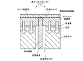
- FIG. 2 shows an example of the structure around the power supply terminal of the wafer mounting table.
- a ceramic sleeve made of an insulating material is adhered to the outer peripheral surface of the portion of the power supply terminal that is inserted into the power supply terminal hole of the cooling member. That is, the power supply terminal is fixed in the hole by the adhesive layer in a state where the power supply terminal is inserted into the power supply terminal hole penetrating the ceramic sleeve in the vertical direction. Since the ceramic sleeve is manufactured by cutting or the like, a certain thickness is required.
- the ceramic sleeve is thick, it is necessary to increase the diameter of the hole for the power supply terminal to be drilled in the cooling member, which may impair the wafer mounting surface and the heat equalization of the wafer. That is, the power supply terminal hole made in the cooling member is a peculiar place where heat is not removed from the heat input from the plasma (arrow in FIG. 2) directly downward, but if the diameter of the hole is large, the peculiar place is also a peculiar place. Since the size is increased, the wafer mounting surface and the heat equalizing property of the wafer are impaired.
- the present invention has been made to solve such a problem, and a main object thereof is to improve the heat equalizing property of the wafer mounting surface and the wafer.
- the wafer mounting table of the present invention An electrostatic chuck with electrostatic adsorption electrodes embedded in a ceramic sintered body, A cooling member that is bonded or bonded to the surface of the electrostatic chuck opposite to the wafer mounting surface to cool the electrostatic chuck, and A hole for a power supply terminal that penetrates the cooling member in the thickness direction, A power supply terminal joined to the electrostatic adsorption electrode from a surface opposite to the wafer mounting surface of the electrostatic chuck and inserted into the power supply terminal hole.
- the outer peripheral surface of the power feeding terminal portion inserted into the power feeding terminal hole is covered with an insulating thin film coated with an insulating material. It is a thing.
- the outer peripheral surface of the power supply terminal that is inserted into the power supply terminal hole is covered with an insulating thin film coated with an insulating material. Therefore, the diameter of the feeding terminal hole provided in the cooling member can be reduced according to the diameter of the portion of the feeding terminal covered with the insulating thin film.
- the hole for the power supply terminal is a peculiar place where heat is not removed from the heat input from the plasma directly downward, but since the diameter of the hole for the power supply terminal can be reduced, the peculiar part can be reduced. As a result, the heat equalizing property of the wafer mounting surface and the wafer is improved.
- the insulating thin film may be an aerosol deposition (AD) film or a thermal spray film.
- AD aerosol deposition
- the AD method (including the plasma AD method) is suitable for accurately forming a thin film of fine ceramic particles.
- the ceramic particles can be formed by the impact solidification phenomenon, it is not necessary to sinter the ceramic particles at a high temperature.
- the insulating thin film may have a thickness of 10 ⁇ m or more and 200 ⁇ m or less. In this way, the diameter of the feeding terminal hole can be made smaller.
- the gap between the outer surface of the insulating thin film and the inner surface of the feeding terminal hole may be 1 mm or less. In this way, the diameter of the feeding terminal hole can be made smaller.
- the vertical sectional view of the main part of the wafer mounting table of this embodiment is A vertical sectional view of a main part of a conventional wafer mounting table.
- FIG. 1 is a vertical cross-sectional view of a main part of the wafer mounting table of the present embodiment.
- the wafer mount is provided with an electrostatic chuck, a cooling member, a hole for a power supply terminal, and a power supply terminal.
- the electrostatic chuck has an electrostatic adsorption electrode embedded in a disk-shaped ceramic sintered body, and when a voltage is applied to the electrostatic adsorption electrode, it is placed on the wafer mounting surface of the electrostatic chuck.
- the wafer (not shown) is electrostatically attracted.
- the cooling member is a metal member having a refrigerant passage (not shown) inside, and cools the electrostatic chuck.
- the power supply terminal hole penetrates the cooling member in the thickness direction.
- the power supply terminal is wax-bonded to the electrostatic adsorption electrode from the surface of the electrostatic chuck opposite to the wafer mounting surface, and is inserted into the power supply terminal hole.
- the material of the power feeding terminal include molybdenum, titanium, nickel and the like.
- the outer peripheral surface of the power feeding terminal portion inserted into the power feeding terminal hole is covered with an insulating thin film coated with an insulating material (for example, alumina).
- the outer peripheral surface of the portion of the feeding terminal inserted into the feeding terminal hole is covered with an insulating thin film coated with an insulating material. Therefore, the diameter of the feeding terminal hole provided in the cooling member can be reduced according to the diameter of the portion of the feeding terminal covered with the insulating thin film.
- the hole for the power supply terminal is a peculiar place where heat is not removed from the heat input from the plasma directly downward, but since the diameter of the hole for the power supply terminal can be reduced, the peculiar part can be reduced. As a result, the heat equalizing property of the wafer mounting surface and the wafer is improved.
- the insulating thin film is preferably an AD film or a thermal sprayed film, and an AD film is more preferable.
- the AD method is suitable for accurately forming a thin film of fine ceramic particles. Further, in the AD method, since the ceramic particles can be formed by the impact solidification phenomenon, it is not necessary to sinter the ceramic particles at a high temperature.
- the insulating thin film preferably has a thickness of 10 ⁇ m or more and 200 ⁇ m or less. Further, the gap between the outer surface of the insulating thin film and the inner surface of the feeding terminal hole is preferably 1 mm or less. In this way, the diameter of the feeding terminal hole can be made smaller.
- a heater electrode may be embedded in the electrostatic chuck, or an RF electrode may be embedded in the electrostatic chuck.
- the present invention can be used for, for example, film forming processes such as semiconductor wafer transfer, exposure, and CVD, and microfabrication such as cleaning, etching, and dicing.
Landscapes
- Engineering & Computer Science (AREA)
- Physics & Mathematics (AREA)
- Condensed Matter Physics & Semiconductors (AREA)
- General Physics & Mathematics (AREA)
- Manufacturing & Machinery (AREA)
- Computer Hardware Design (AREA)
- Microelectronics & Electronic Packaging (AREA)
- Power Engineering (AREA)
- Mechanical Engineering (AREA)
- Container, Conveyance, Adherence, Positioning, Of Wafer (AREA)
Abstract
Description
セラミック焼結体に静電吸着用電極が埋設された静電チャックと、
前記静電チャックのウエハ載置面とは反対側の面に接着又は接合され、前記静電チャックを冷却する冷却部材と、
前記冷却部材を厚さ方向に貫通する給電端子用穴と、
前記静電チャックのウエハ載置面とは反対側の面から前記静電吸着用電極に接合され、前記給電端子用穴に挿入された給電端子と、
を備え、
前記給電端子のうち前記給電端子用穴に挿入されている部分の外周面は、絶縁材料をコーティングした絶縁薄膜で覆われている、
ものである。 The wafer mounting table of the present invention
An electrostatic chuck with electrostatic adsorption electrodes embedded in a ceramic sintered body,
A cooling member that is bonded or bonded to the surface of the electrostatic chuck opposite to the wafer mounting surface to cool the electrostatic chuck, and
A hole for a power supply terminal that penetrates the cooling member in the thickness direction,
A power supply terminal joined to the electrostatic adsorption electrode from a surface opposite to the wafer mounting surface of the electrostatic chuck and inserted into the power supply terminal hole.
With
The outer peripheral surface of the power feeding terminal portion inserted into the power feeding terminal hole is covered with an insulating thin film coated with an insulating material.
It is a thing.
Claims (4)
- セラミック焼結体に静電吸着用電極が埋設された静電チャックと、
前記静電チャックのウエハ載置面とは反対側の面に接着又は接合され、前記静電チャックを冷却する冷却部材と、
前記冷却部材を厚さ方向に貫通する給電端子用穴と、
前記静電チャックのウエハ載置面とは反対側の面から前記静電吸着用電極に接合され、前記給電端子用穴に挿入された給電端子と、
を備え、
前記給電端子のうち前記給電端子用穴に挿入されている部分の外周面は、絶縁材料をコーティングした絶縁薄膜で覆われている、
ウエハ載置台。 An electrostatic chuck with electrostatic adsorption electrodes embedded in a ceramic sintered body,
A cooling member that is bonded or bonded to the surface of the electrostatic chuck opposite to the wafer mounting surface to cool the electrostatic chuck, and
A hole for a power supply terminal that penetrates the cooling member in the thickness direction,
A power supply terminal joined to the electrostatic adsorption electrode from a surface opposite to the wafer mounting surface of the electrostatic chuck and inserted into the power supply terminal hole.
With
The outer peripheral surface of the power feeding terminal portion inserted into the power feeding terminal hole is covered with an insulating thin film coated with an insulating material.
Wafer mount. - 前記絶縁薄膜は、エアロゾルデポジション膜又は溶射膜である、
請求項1に記載のウエハ載置台。 The insulating thin film is an aerosol deposition film or a thermal sprayed film.
The wafer mounting table according to claim 1. - 前記絶縁薄膜は、厚みが10μm以上200μm以下である、
請求項1又は2に記載のウエハ載置台。 The insulating thin film has a thickness of 10 μm or more and 200 μm or less.
The wafer mounting table according to claim 1 or 2. - 前記絶縁薄膜の外面と前記給電端子用穴の内面との隙間は、1mm以下である、
請求項1~3のいずれか1項に記載のウエハ載置台。 The gap between the outer surface of the insulating thin film and the inner surface of the feeding terminal hole is 1 mm or less.
The wafer mounting table according to any one of claims 1 to 3.
Priority Applications (4)
| Application Number | Priority Date | Filing Date | Title |
|---|---|---|---|
| CN202080047772.4A CN114026681A (en) | 2019-06-28 | 2020-06-10 | Wafer mounting table |
| KR1020217033957A KR102632768B1 (en) | 2019-06-28 | 2020-06-10 | wafer placement table |
| JP2021528135A JP7214868B2 (en) | 2019-06-28 | 2020-06-10 | Wafer table |
| US17/465,943 US11948825B2 (en) | 2019-06-28 | 2021-09-03 | Wafer placement table |
Applications Claiming Priority (2)
| Application Number | Priority Date | Filing Date | Title |
|---|---|---|---|
| JP2019-121490 | 2019-06-28 | ||
| JP2019121490 | 2019-06-28 |
Related Child Applications (1)
| Application Number | Title | Priority Date | Filing Date |
|---|---|---|---|
| US17/465,943 Continuation US11948825B2 (en) | 2019-06-28 | 2021-09-03 | Wafer placement table |
Publications (1)
| Publication Number | Publication Date |
|---|---|
| WO2020261992A1 true WO2020261992A1 (en) | 2020-12-30 |
Family
ID=74061068
Family Applications (1)
| Application Number | Title | Priority Date | Filing Date |
|---|---|---|---|
| PCT/JP2020/022832 WO2020261992A1 (en) | 2019-06-28 | 2020-06-10 | Wafer placement stand |
Country Status (5)
| Country | Link |
|---|---|
| US (1) | US11948825B2 (en) |
| JP (1) | JP7214868B2 (en) |
| KR (1) | KR102632768B1 (en) |
| CN (1) | CN114026681A (en) |
| WO (1) | WO2020261992A1 (en) |
Citations (1)
| Publication number | Priority date | Publication date | Assignee | Title |
|---|---|---|---|---|
| JP2003179127A (en) * | 2001-12-11 | 2003-06-27 | Taiheiyo Cement Corp | Power feed terminal of an electrostatic chuck |
Family Cites Families (14)
| Publication number | Priority date | Publication date | Assignee | Title |
|---|---|---|---|---|
| JPH07297265A (en) * | 1994-04-26 | 1995-11-10 | Shin Etsu Chem Co Ltd | Electrostatic chuck |
| JP4034145B2 (en) | 2002-08-09 | 2008-01-16 | 住友大阪セメント株式会社 | Susceptor device |
| JP4346877B2 (en) * | 2002-08-29 | 2009-10-21 | 東京エレクトロン株式会社 | Electrostatic adsorption device and processing device |
| JP2007258615A (en) | 2006-03-24 | 2007-10-04 | Ngk Insulators Ltd | Electrostatic chuck |
| US20080062609A1 (en) * | 2006-08-10 | 2008-03-13 | Shinji Himori | Electrostatic chuck device |
| JP2008160093A (en) | 2006-11-29 | 2008-07-10 | Toto Ltd | Electrostatic chuck and manufacturing method thereof, and substrate-treating device |
| JP5604888B2 (en) * | 2009-12-21 | 2014-10-15 | 住友大阪セメント株式会社 | Manufacturing method of electrostatic chuck |
| JP6119430B2 (en) * | 2013-05-31 | 2017-04-26 | 住友大阪セメント株式会社 | Electrostatic chuck device |
| KR101994006B1 (en) * | 2014-06-23 | 2019-06-27 | 니혼도꾸슈도교 가부시키가이샤 | Electrostatic chuck |
| KR102233925B1 (en) * | 2014-11-20 | 2021-03-30 | 스미토모 오사카 세멘토 가부시키가이샤 | Electrostatic chuck device |
| KR101950897B1 (en) * | 2015-09-25 | 2019-02-21 | 스미토모 오사카 세멘토 가부시키가이샤 | Electrostatic chuck device |
| US11107719B2 (en) * | 2016-01-12 | 2021-08-31 | Sumitomo Osaka Cement Co., Ltd. | Electrostatic chuck device and method for manufacturing electrostatic chuck device |
| US10923381B2 (en) * | 2016-01-19 | 2021-02-16 | Sumitomo Osaka Cement Co., Ltd. | Electrostatic chuck device |
| US11551962B2 (en) * | 2018-03-30 | 2023-01-10 | Sumitomo Osaka Cement Co., Ltd. | Ceramic substrate and susceptor |
-
2020
- 2020-06-10 WO PCT/JP2020/022832 patent/WO2020261992A1/en active Application Filing
- 2020-06-10 CN CN202080047772.4A patent/CN114026681A/en active Pending
- 2020-06-10 KR KR1020217033957A patent/KR102632768B1/en active IP Right Grant
- 2020-06-10 JP JP2021528135A patent/JP7214868B2/en active Active
-
2021
- 2021-09-03 US US17/465,943 patent/US11948825B2/en active Active
Patent Citations (1)
| Publication number | Priority date | Publication date | Assignee | Title |
|---|---|---|---|---|
| JP2003179127A (en) * | 2001-12-11 | 2003-06-27 | Taiheiyo Cement Corp | Power feed terminal of an electrostatic chuck |
Also Published As
| Publication number | Publication date |
|---|---|
| JPWO2020261992A1 (en) | 2020-12-30 |
| US20210398840A1 (en) | 2021-12-23 |
| CN114026681A (en) | 2022-02-08 |
| KR20210141641A (en) | 2021-11-23 |
| JP7214868B2 (en) | 2023-01-30 |
| US11948825B2 (en) | 2024-04-02 |
| KR102632768B1 (en) | 2024-02-01 |
Similar Documents
| Publication | Publication Date | Title |
|---|---|---|
| KR101994006B1 (en) | Electrostatic chuck | |
| JP6380177B2 (en) | Electrostatic chuck device | |
| US20160276198A1 (en) | Electrostatic chuck | |
| US10622239B2 (en) | Electrostatic chuck device | |
| US11348819B2 (en) | Electrostatic chuck device | |
| WO2017010307A1 (en) | Wafer holding body | |
| JP6520160B2 (en) | Electrostatic chuck device | |
| WO2020261992A1 (en) | Wafer placement stand | |
| JP7214502B2 (en) | sample holder | |
| US20220259727A1 (en) | Substrate heating device, substrate heating method, and method of manufacturing substrate heater | |
| JP7430489B2 (en) | Electrostatic chuck, electrostatic chuck device | |
| JP4890428B2 (en) | Electrostatic chuck | |
| WO2021002168A1 (en) | Ceramic heater with shaft | |
| JP7303302B2 (en) | ceramic heater with shaft | |
| JP7214867B2 (en) | electrostatic chuck | |
| WO2021010063A1 (en) | Ceramic heater with shaft | |
| JP2022094466A (en) | Electrostatic chuck device | |
| JP2023055342A (en) | Substrate holding member | |
| JP2023056923A (en) | Substrate holding member |
Legal Events
| Date | Code | Title | Description |
|---|---|---|---|
| 121 | Ep: the epo has been informed by wipo that ep was designated in this application |
Ref document number: 20832447 Country of ref document: EP Kind code of ref document: A1 |
|
| ENP | Entry into the national phase |
Ref document number: 2021528135 Country of ref document: JP Kind code of ref document: A |
|
| ENP | Entry into the national phase |
Ref document number: 20217033957 Country of ref document: KR Kind code of ref document: A |
|
| NENP | Non-entry into the national phase |
Ref country code: DE |
|
| 122 | Ep: pct application non-entry in european phase |
Ref document number: 20832447 Country of ref document: EP Kind code of ref document: A1 |