WO2020255805A1 - 半導体装置、及び半導体装置の製造方法 - Google Patents
半導体装置、及び半導体装置の製造方法 Download PDFInfo
- Publication number
- WO2020255805A1 WO2020255805A1 PCT/JP2020/022738 JP2020022738W WO2020255805A1 WO 2020255805 A1 WO2020255805 A1 WO 2020255805A1 JP 2020022738 W JP2020022738 W JP 2020022738W WO 2020255805 A1 WO2020255805 A1 WO 2020255805A1
- Authority
- WO
- WIPO (PCT)
- Prior art keywords
- insulating film
- dielectric constant
- low dielectric
- semiconductor device
- region
- Prior art date
- Legal status (The legal status is an assumption and is not a legal conclusion. Google has not performed a legal analysis and makes no representation as to the accuracy of the status listed.)
- Ceased
Links
Images

















Classifications
-
- H—ELECTRICITY
- H10—SEMICONDUCTOR DEVICES; ELECTRIC SOLID-STATE DEVICES NOT OTHERWISE PROVIDED FOR
- H10W—GENERIC PACKAGES, INTERCONNECTIONS, CONNECTORS OR OTHER CONSTRUCTIONAL DETAILS OF DEVICES COVERED BY CLASS H10
- H10W20/00—Interconnections in chips, wafers or substrates
- H10W20/20—Interconnections within wafers or substrates, e.g. through-silicon vias [TSV]
-
- H—ELECTRICITY
- H10—SEMICONDUCTOR DEVICES; ELECTRIC SOLID-STATE DEVICES NOT OTHERWISE PROVIDED FOR
- H10D—INORGANIC ELECTRIC SEMICONDUCTOR DEVICES
- H10D30/00—Field-effect transistors [FET]
- H10D30/60—Insulated-gate field-effect transistors [IGFET]
- H10D30/601—Insulated-gate field-effect transistors [IGFET] having lightly-doped drain or source extensions, e.g. LDD IGFETs or DDD IGFETs
-
- H—ELECTRICITY
- H10—SEMICONDUCTOR DEVICES; ELECTRIC SOLID-STATE DEVICES NOT OTHERWISE PROVIDED FOR
- H10D—INORGANIC ELECTRIC SEMICONDUCTOR DEVICES
- H10D30/00—Field-effect transistors [FET]
- H10D30/01—Manufacture or treatment
- H10D30/021—Manufacture or treatment of FETs having insulated gates [IGFET]
- H10D30/031—Manufacture or treatment of FETs having insulated gates [IGFET] of thin-film transistors [TFT]
- H10D30/0321—Manufacture or treatment of FETs having insulated gates [IGFET] of thin-film transistors [TFT] comprising silicon, e.g. amorphous silicon or polysilicon
- H10D30/0323—Manufacture or treatment of FETs having insulated gates [IGFET] of thin-film transistors [TFT] comprising silicon, e.g. amorphous silicon or polysilicon comprising monocrystalline silicon
-
- H—ELECTRICITY
- H10—SEMICONDUCTOR DEVICES; ELECTRIC SOLID-STATE DEVICES NOT OTHERWISE PROVIDED FOR
- H10D—INORGANIC ELECTRIC SEMICONDUCTOR DEVICES
- H10D30/00—Field-effect transistors [FET]
- H10D30/60—Insulated-gate field-effect transistors [IGFET]
- H10D30/67—Thin-film transistors [TFT]
- H10D30/674—Thin-film transistors [TFT] characterised by the active materials
- H10D30/6741—Group IV materials, e.g. germanium or silicon carbide
- H10D30/6743—Silicon
- H10D30/6744—Monocrystalline silicon
-
- H—ELECTRICITY
- H10—SEMICONDUCTOR DEVICES; ELECTRIC SOLID-STATE DEVICES NOT OTHERWISE PROVIDED FOR
- H10D—INORGANIC ELECTRIC SEMICONDUCTOR DEVICES
- H10D64/00—Electrodes of devices having potential barriers
- H10D64/20—Electrodes characterised by their shapes, relative sizes or dispositions
- H10D64/23—Electrodes carrying the current to be rectified, amplified, oscillated or switched, e.g. sources, drains, anodes or cathodes
- H10D64/251—Source or drain electrodes for field-effect devices
- H10D64/257—Source or drain electrodes for field-effect devices for lateral devices wherein the source or drain electrodes are characterised by top-view geometrical layouts, e.g. interdigitated, semi-circular, annular or L-shaped electrodes
-
- H—ELECTRICITY
- H10—SEMICONDUCTOR DEVICES; ELECTRIC SOLID-STATE DEVICES NOT OTHERWISE PROVIDED FOR
- H10D—INORGANIC ELECTRIC SEMICONDUCTOR DEVICES
- H10D64/00—Electrodes of devices having potential barriers
- H10D64/20—Electrodes characterised by their shapes, relative sizes or dispositions
- H10D64/23—Electrodes carrying the current to be rectified, amplified, oscillated or switched, e.g. sources, drains, anodes or cathodes
- H10D64/251—Source or drain electrodes for field-effect devices
- H10D64/258—Source or drain electrodes for field-effect devices characterised by the relative positions of the source or drain electrodes with respect to the gate electrode
-
- H—ELECTRICITY
- H10—SEMICONDUCTOR DEVICES; ELECTRIC SOLID-STATE DEVICES NOT OTHERWISE PROVIDED FOR
- H10D—INORGANIC ELECTRIC SEMICONDUCTOR DEVICES
- H10D86/00—Integrated devices formed in or on insulating or conducting substrates, e.g. formed in silicon-on-insulator [SOI] substrates or on stainless steel or glass substrates
- H10D86/01—Manufacture or treatment
-
- H—ELECTRICITY
- H10—SEMICONDUCTOR DEVICES; ELECTRIC SOLID-STATE DEVICES NOT OTHERWISE PROVIDED FOR
- H10D—INORGANIC ELECTRIC SEMICONDUCTOR DEVICES
- H10D86/00—Integrated devices formed in or on insulating or conducting substrates, e.g. formed in silicon-on-insulator [SOI] substrates or on stainless steel or glass substrates
- H10D86/201—Integrated devices formed in or on insulating or conducting substrates, e.g. formed in silicon-on-insulator [SOI] substrates or on stainless steel or glass substrates the substrates comprising an insulating layer on a semiconductor body, e.g. SOI
-
- H—ELECTRICITY
- H10—SEMICONDUCTOR DEVICES; ELECTRIC SOLID-STATE DEVICES NOT OTHERWISE PROVIDED FOR
- H10W—GENERIC PACKAGES, INTERCONNECTIONS, CONNECTORS OR OTHER CONSTRUCTIONAL DETAILS OF DEVICES COVERED BY CLASS H10
- H10W20/00—Interconnections in chips, wafers or substrates
- H10W20/01—Manufacture or treatment
- H10W20/021—Manufacture or treatment of interconnections within wafers or substrates
- H10W20/023—Manufacture or treatment of interconnections within wafers or substrates the interconnections being through-semiconductor vias
-
- H—ELECTRICITY
- H10—SEMICONDUCTOR DEVICES; ELECTRIC SOLID-STATE DEVICES NOT OTHERWISE PROVIDED FOR
- H10W—GENERIC PACKAGES, INTERCONNECTIONS, CONNECTORS OR OTHER CONSTRUCTIONAL DETAILS OF DEVICES COVERED BY CLASS H10
- H10W20/00—Interconnections in chips, wafers or substrates
- H10W20/01—Manufacture or treatment
- H10W20/071—Manufacture or treatment of dielectric parts thereof
- H10W20/072—Manufacture or treatment of dielectric parts thereof of dielectric parts comprising air gaps
-
- H—ELECTRICITY
- H10—SEMICONDUCTOR DEVICES; ELECTRIC SOLID-STATE DEVICES NOT OTHERWISE PROVIDED FOR
- H10W—GENERIC PACKAGES, INTERCONNECTIONS, CONNECTORS OR OTHER CONSTRUCTIONAL DETAILS OF DEVICES COVERED BY CLASS H10
- H10W20/00—Interconnections in chips, wafers or substrates
- H10W20/01—Manufacture or treatment
- H10W20/071—Manufacture or treatment of dielectric parts thereof
- H10W20/074—Manufacture or treatment of dielectric parts thereof of dielectric parts comprising thin functional dielectric layers, e.g. dielectric etch-stop, barrier, capping or liner layers
- H10W20/076—Manufacture or treatment of dielectric parts thereof of dielectric parts comprising thin functional dielectric layers, e.g. dielectric etch-stop, barrier, capping or liner layers in via holes or trenches
-
- H—ELECTRICITY
- H10—SEMICONDUCTOR DEVICES; ELECTRIC SOLID-STATE DEVICES NOT OTHERWISE PROVIDED FOR
- H10W—GENERIC PACKAGES, INTERCONNECTIONS, CONNECTORS OR OTHER CONSTRUCTIONAL DETAILS OF DEVICES COVERED BY CLASS H10
- H10W20/00—Interconnections in chips, wafers or substrates
- H10W20/01—Manufacture or treatment
- H10W20/071—Manufacture or treatment of dielectric parts thereof
- H10W20/081—Manufacture or treatment of dielectric parts thereof by forming openings in the dielectric parts
- H10W20/089—Manufacture or treatment of dielectric parts thereof by forming openings in the dielectric parts using processes for implementing desired shapes or dispositions of the openings, e.g. double patterning
-
- H—ELECTRICITY
- H10—SEMICONDUCTOR DEVICES; ELECTRIC SOLID-STATE DEVICES NOT OTHERWISE PROVIDED FOR
- H10W—GENERIC PACKAGES, INTERCONNECTIONS, CONNECTORS OR OTHER CONSTRUCTIONAL DETAILS OF DEVICES COVERED BY CLASS H10
- H10W20/00—Interconnections in chips, wafers or substrates
- H10W20/40—Interconnections external to wafers or substrates, e.g. back-end-of-line [BEOL] metallisations or vias connecting to gate electrodes
-
- H—ELECTRICITY
- H10—SEMICONDUCTOR DEVICES; ELECTRIC SOLID-STATE DEVICES NOT OTHERWISE PROVIDED FOR
- H10W—GENERIC PACKAGES, INTERCONNECTIONS, CONNECTORS OR OTHER CONSTRUCTIONAL DETAILS OF DEVICES COVERED BY CLASS H10
- H10W20/00—Interconnections in chips, wafers or substrates
- H10W20/40—Interconnections external to wafers or substrates, e.g. back-end-of-line [BEOL] metallisations or vias connecting to gate electrodes
- H10W20/41—Interconnections external to wafers or substrates, e.g. back-end-of-line [BEOL] metallisations or vias connecting to gate electrodes characterised by their conductive parts
- H10W20/435—Cross-sectional shapes or dispositions of interconnections
-
- H—ELECTRICITY
- H10—SEMICONDUCTOR DEVICES; ELECTRIC SOLID-STATE DEVICES NOT OTHERWISE PROVIDED FOR
- H10W—GENERIC PACKAGES, INTERCONNECTIONS, CONNECTORS OR OTHER CONSTRUCTIONAL DETAILS OF DEVICES COVERED BY CLASS H10
- H10W20/00—Interconnections in chips, wafers or substrates
- H10W20/40—Interconnections external to wafers or substrates, e.g. back-end-of-line [BEOL] metallisations or vias connecting to gate electrodes
- H10W20/45—Interconnections external to wafers or substrates, e.g. back-end-of-line [BEOL] metallisations or vias connecting to gate electrodes characterised by their insulating parts
- H10W20/46—Interconnections external to wafers or substrates, e.g. back-end-of-line [BEOL] metallisations or vias connecting to gate electrodes characterised by their insulating parts comprising air gaps
-
- H—ELECTRICITY
- H10—SEMICONDUCTOR DEVICES; ELECTRIC SOLID-STATE DEVICES NOT OTHERWISE PROVIDED FOR
- H10W—GENERIC PACKAGES, INTERCONNECTIONS, CONNECTORS OR OTHER CONSTRUCTIONAL DETAILS OF DEVICES COVERED BY CLASS H10
- H10W20/00—Interconnections in chips, wafers or substrates
- H10W20/40—Interconnections external to wafers or substrates, e.g. back-end-of-line [BEOL] metallisations or vias connecting to gate electrodes
- H10W20/45—Interconnections external to wafers or substrates, e.g. back-end-of-line [BEOL] metallisations or vias connecting to gate electrodes characterised by their insulating parts
- H10W20/47—Interconnections external to wafers or substrates, e.g. back-end-of-line [BEOL] metallisations or vias connecting to gate electrodes characterised by their insulating parts comprising two or more dielectric layers having different properties, e.g. different dielectric constants
-
- H—ELECTRICITY
- H10—SEMICONDUCTOR DEVICES; ELECTRIC SOLID-STATE DEVICES NOT OTHERWISE PROVIDED FOR
- H10W—GENERIC PACKAGES, INTERCONNECTIONS, CONNECTORS OR OTHER CONSTRUCTIONAL DETAILS OF DEVICES COVERED BY CLASS H10
- H10W20/00—Interconnections in chips, wafers or substrates
- H10W20/40—Interconnections external to wafers or substrates, e.g. back-end-of-line [BEOL] metallisations or vias connecting to gate electrodes
- H10W20/495—Capacitive arrangements or effects of, or between wiring layers
Definitions
- the present disclosure relates to a semiconductor device and a method for manufacturing the semiconductor device.
- the front end of a mobile communication terminal such as a mobile phone is equipped with a high frequency switch (RF-SW) that handles high frequency (Radio Frequency: RF) electric signals.
- RF-SW high frequency switch
- the resistance also referred to as the on resistance
- the capacitance of the FET in the off state It is desired to reduce (also called off capacity). That is, in a high frequency switch, it is desired to reduce the product (Ron * Coff) of the on-resistance and the off-capacity, and various studies have been conducted (see, for example, Patent Document 1).
- the semiconductor device is provided on the gate electrode, the semiconductor layer having the source region and the drain region between the gate electrodes, the source region, and the drain region, respectively.
- a first low dielectric constant region provided in at least one region below the lower surface, between the contact plug and the gate electrode in the in-plane direction, and the first low dielectric constant region in the stacking direction. It is provided with a second low dielectric constant region provided in at least one region below the region, and the second low dielectric constant region is at least a part of a plane region in which the first low dielectric constant region is provided. It is provided in a different plane region.
- the method for manufacturing a semiconductor device includes a step of forming a gate electrode on the upper surface side of a semiconductor layer, and forming a source region and a drain region in the semiconductor layer with the gate electrode in between.
- the first low includes a step of forming a second low dielectric constant region between the contact plug and the gate electrode and in at least any region below the first low dielectric constant region in the stacking direction.
- the second low dielectric constant region is formed in a plane region that is at least partially different from the plane region in which the dielectric constant region is formed.
- the first metal is provided between each of the first metals in the in-plane direction of the semiconductor layer and in the stacking direction of the semiconductor layers.
- a first low dielectric constant region in at least one region below the lower surface of the surface, between the contact plug and the gate electrode in the in-plane direction, and above the first low dielectric constant region in the stacking direction.
- FIG. 7 It is a schematic diagram which showed the positional relationship in the XY in-plane direction of the 1st low dielectric constant region, the 2nd low dielectric constant region, and a multilayer wiring part in the semiconductor device shown in FIG. 7. It is a vertical cross-sectional view which shows the cross-sectional structure in the XV-XV line of FIG. It is a vertical cross-sectional view which shows the cross-sectional structure in the XVIA-XVIB line of FIG. It is a vertical cross-sectional view which shows the cross-sectional structure in the XVIIB-XVIIC line of FIG. It is a vertical cross-sectional view which shows the cross-sectional structure in the XVIIIC-XVIIID line of FIG.
- FIG. 1 is a schematic diagram showing a configuration of a high-frequency switch having a number of input / output ports of 1 to 10
- FIG. 2 is a schematic diagram showing a configuration of a high-frequency switch having a number of input / output ports of 1 to 1. is there.
- the high frequency switch is an electronic component mainly used for signal processing in the radio frequency (Radio Frequency: RF) band.
- the high frequency switch is used, for example, in the front end of a mobile information terminal such as a mobile phone.
- High-frequency switches include SPST (Single Pole Single Throw: single pole single throw), SPDT (Single Pole Double Throw: single pole double throw), SP3T, ... SPNT (N is a real number), etc., depending on the number of input / output ports. It can take various configurations.
- the high frequency switch 1 shown in FIG. 1 is an example of an SP10T switch.
- the high-frequency switch 1 which is an SP10T switch includes, for example, one pole connected to the antenna ANT and ten contacts, and can control the contacts connected from among the ten contacts.
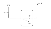
- the high frequency switch 1A shown in FIG. 2 is an example of an SPST switch.
- the high frequency switch 1A, which is an SPST switch includes, for example, one pole connected to the antenna ANT and one contact, and can control the on or off of one contact.
- the high frequency switch can have a configuration other than the configurations shown in FIGS. 1 and 2.
- the high-frequency switch can have various configurations by combining the circuits of the SPST switch shown in FIG.
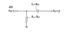
- FIG. 3 is a circuit diagram showing an equivalent circuit of the high frequency switch 1A shown in FIG.
- FIG. 4 is a circuit diagram showing an equivalent circuit when the high frequency switch 1A shown in FIG. 2 is in the on state
- FIG. 5 is a circuit diagram showing an equivalent circuit when the high frequency switch 1A shown in FIG. 2 is in the off state. is there.
- the high-frequency switch 1A which is an SPST, includes, for example, a first port Port1 connected to an antenna ANT, a second port Port2 on the output side, a first switching element FET1, and a second switching element FET2. And.
- the first switching element FET1 is provided between the first port Port1 and the ground, and the second switching element FET2 is provided between the first port Port1 and the second port Port2.
- Such a high frequency switch 1A controls an on state or an off state of the switch by applying control voltages Vc1 and Vc2 to the gates of the first switching element FET1 and the second switching element FET2 via a resistor. Can be done.
- the second switching element FET 2 When the high frequency switch 1A is on, the second switching element FET 2 is in a conductive state and the first switching element FET 1 is in a non-conducting state, as shown in FIG. Further, when the high frequency switch 1A is in the off state, as shown in FIG. 5, the first switching element FET1 is in a conductive state and the second switching element FET2 is in a non-conducting state.
- the first switching element FET1 and the second switching element FET2 are equivalent to a resistor in a conductive state and equivalent to a capacitor in a non-conducting state. Therefore, in the first switching element FET1 and the second switching element FET2, a resistance called on resistance is generated in the conductive state, and a capacitance called off capacitance is generated in the non-conducting state.
- the on-resistance and off capacitance of the first switching element FET1 and the second switching element FET2 are Ron [ ⁇ mm] and Coff [fF / mm] per unit length of the field-effect transistor, and the field-effect transistor.
- the gate widths Wg 1 and Wg 2 [mm] they can be expressed as Ron / Wg 1 , Ron / Wg 2 , Coff * Wg 1 , and Coff * Wg 2 , respectively. That is, in the field effect transistor, the on-resistance is inversely proportional to the gate widths Wg 1 and Wg 2 , and the off capacitance is proportional to the gate widths Wg 1 and Wg 2 .
- the loss due to the off capacitance becomes large.
- the on-resistance of the field-effect transistor does not depend on the frequency of the signal, but the off capacitance increases as the frequency of the signal increases. Therefore, in a high frequency switch that handles high frequency signals, the loss due to off capacitance becomes even larger.
- the technology related to this disclosure was made in view of the above circumstances.
- the technique according to the present disclosure is to reduce the on-resistance and the off capacitance of a field-effect transistor by reducing the parasitic capacitance of a semiconductor device such as a field-effect transistor.
- the technique according to the present disclosure can be suitably used for a high frequency switch or the like provided in an electronic device that handles a high frequency signal.
- FIG. 6 is a plan view showing the overall configuration of the semiconductor device according to the present embodiment.
- the semiconductor device 10 includes, for example, a gate electrode 20 provided on a semiconductor layer (not shown), a source electrode 30S, and a drain electrode 30D.
- the gate electrode 20 is shaded.
- the semiconductor device 10 is, for example, a field effect transistor for a high-frequency device constituting the first switching element FET1 or the second switching element FET2 included in the high-frequency switch 1A shown in FIG.
- the gate electrode 20 is provided with a multi-finger structure having a plurality of finger portions 21 extended in one direction and a connecting portion 22 for connecting the plurality of finger portions 21 to each other.
- the gate width Wg of the field-effect transistor used in the high-frequency switch is larger than that of the field-effect transistor used in a logic circuit or the like in order to reduce the loss, and is, for example, several hundred ⁇ m to several mm. Further, the length (finger length) L21 of the finger portion 21 is, for example, several tens of ⁇ m.
- the connecting portion 22 is connected to a gate contact (not shown).
- the direction in which the finger portion 21 of the gate electrode 20 extends is the Y direction. Further, the direction orthogonal to the Y direction and extending the connecting portion 22 is defined as the X direction. Further, a direction orthogonal to both the X direction and the Y direction (that is, a direction perpendicular to the plane of the semiconductor layer (not shown) is defined as the Z direction.
- the source electrode 30S is a connecting portion 32S that connects a finger portion 31S extended in one direction (for example, the Y direction) and a plurality of finger portions 31S and is connected to a source contact (not shown). Has.
- the drain electrode 30D has a finger portion 31D extended in one direction (for example, the Y direction) and a connecting portion 32D that connects a plurality of finger portions 31D and is connected to a drain contact (not shown).
- the finger portion 21 of the gate electrode 20, the finger portion 31S of the source electrode 30S, and the finger portion 31D of the drain electrode 30D are arranged inside the active region AA activated by the introduction of conductive impurities. Specifically, the finger portions 31S of the source electrode 30S and the finger portions 31D of the drain electrode 30D are alternately arranged between the finger portions 21 of the gate electrode 20.
- the connecting portion 22 of the gate electrode 20, the connecting portion 32S of the source electrode 30S, and the connecting portion 32D of the drain electrode 30D are arranged in an element separation region (not shown) provided outside the active region AA.
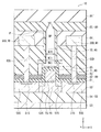
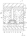
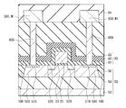
- FIG. 7 is a vertical cross-sectional view showing a cross-sectional structure taken along line VII-VII of FIG.
- FIG. 7 shows a cross-sectional configuration including one of the finger portions 21 of the gate electrode 20, the finger portions 31S of the source electrode 30S arranged on both sides of the finger portion 21, and the finger portions 31D of the drain electrode 30D.
- the semiconductor device 10 includes, for example, the above-mentioned gate electrode 20, the semiconductor layer 50, the contact plugs 60S and 60D, the above-mentioned source electrode 30S, and the first metal M1 including the drain electrode 30D.
- a first low dielectric constant region 70 and a second low dielectric constant region 71 are provided.
- the gate electrode 20 is provided on the semiconductor layer 50 via the gate insulating film 23.
- the gate electrode 20 may be made of polysilicon with a thickness of, for example, 100 nm to 200 nm.
- the gate insulating film 23 may be made of silicon oxide (SiO x ) having a thickness of 5 nm to 15 nm, for example.
- the semiconductor layer 50 may be made of a semiconductor such as silicon (Si), for example.
- the semiconductor layer 50 is provided with a source region 50S and a drain region 50D made of first conductive type (n +) silicon on both sides of the gate electrode 20. Further, on the surface side of the source region 50S and the drain region 50D, a low resistance composed of a higher concentration first conductive type (n ++) silicon or silicide for connection with the contact plugs 60S and 60D. Areas 51S and 51D are provided. Further, between the source region 50S and the gate electrode 20, and between the drain region 50D and the gate electrode 20, extension regions 52S and 52D composed of low-concentration first conductive type (n ⁇ ) silicon are formed. Provided.
- the semiconductor layer 50 is provided on the support substrate 53 via, for example, the embedded oxide film 54.
- the support substrate 53 may be composed of, for example, a high resistance silicon (Si) substrate
- the embedded oxide film 54 may be composed of, for example, silicon oxide (SiO x ). That is, the support substrate 53, the embedded oxide film 54, and the semiconductor layer 50 can form a so-called SOI (Silicon On Insulator) substrate 55.
- SOI Silicon On Insulator
- the support substrate 53 of the SOI substrate 55 is a high resistance silicon substrate
- the technique according to the present disclosure is not limited to the above examples.
- the support substrate 53 may be a sapphire substrate.
- the SOI substrate 55 can form a so-called SOS (Silicon On Sapphire) substrate. Since the sapphire substrate has an insulating property, the field-effect transistor formed on the SOS substrate exhibits characteristics closer to those of a compound-based field-effect transistor such as GaAs.
- the technique according to the present disclosure is not limited to the case where the support substrate 53 is an SOI substrate or an SOS substrate, and is similarly applicable when the support substrate 53 is a bulk silicon substrate.
- the contact plugs 60S and 60D are provided on the low resistance regions 51S and 51D on the surface of the source region 50S and the drain region 50D.
- the contact plugs 60S and 60D can be configured by, for example, laminating a titanium (Ti) layer, a titanium nitride (TiN) layer, and a tungsten (W) layer in this order from the semiconductor layer 50 side.
- the titanium layer is provided to reduce the contact resistance between the contact plugs 60S and 60D and the lower low resistance regions 51S and 51D.
- the titanium nitride layer is provided as a barrier metal that suppresses diffusion of silicon or the like from the semiconductor layer 50 to the tungsten layer.
- the first metal M1 includes, for example, a source electrode 30S provided on the contact plug 60S and a drain electrode 30D provided on the contact plug 60D.
- the first metal M1 may be made of, for example, aluminum (Al) having a thickness of 500 nm to 1000 nm.
- the first low dielectric constant region 70 is, for example, at least between each of the first metal M1s in the XY in-plane direction of the semiconductor layer 50 and below the lower surface of the first metal M1 in the Z lamination direction of the semiconductor layer 50. It is provided in that area. Specifically, the first low dielectric constant region 70 is located between the source electrode 30S and the drain electrode 30D in the XY in-plane direction of the semiconductor layer 50, and from the lower surface of the first metal M1 in the Z stacking direction of the semiconductor layer 50. Is also below and is provided in the region above the gate electrode 20.
- the first low dielectric constant region 70 may be continuously provided up to a region further above the above-mentioned region in the Z stacking direction.
- the first low dielectric constant region 70 is a region between each of the first metal M1s in the XY in-plane direction of the semiconductor layer 50 and between the lower surface and the upper surface of the first metal M1 in the Z lamination direction. It may be further provided in.
- the 1 low dielectric constant region 70 may be further provided between each of the first metal M1s in the XY in-plane direction of the semiconductor layer 50 and in a region above the upper surface of the first metal M1 in the Z lamination direction. Good.
- the second low dielectric constant region 71 is the first low dielectric constant region 70 between each of the contact plugs 60S and 60D in the in-plane direction of the semiconductor layer 50 and the gate electrode 20 and in the Z stacking direction of the semiconductor layer 50. It is provided in at least one area below. Specifically, the second low dielectric constant region 71 is provided on both side surfaces of the gate electrode 20 in the XY in-plane direction of the semiconductor layer 50. The second low dielectric constant region 71 may be provided continuously with the first low dielectric constant region 70, or may be provided separately from the first low dielectric constant region 70.
- At least a part of the second low dielectric constant region 71 is provided in a region different from the region where the first low dielectric constant region 70 is provided when the semiconductor layer 50 is viewed in a plan view from the stacking direction Z. Specifically, at least a part of the second low dielectric constant region 71 is provided in the outer peripheral region of the region where the first low dielectric constant region 70 is provided in the XY in-plane direction of the semiconductor layer 50. According to this, the semiconductor device 10 can form the first low dielectric constant region 70 and the second low dielectric constant region 71 in a more complicated shape.
- FIG. 8 is a vertical cross-sectional view schematically showing the off capacitance of a general field effect transistor 11 for each element.
- the components corresponding to the components of the semiconductor device 10 shown in FIG. 7 are designated by the same reference numerals.
- the off capacitance of the field effect transistor 11 having a general structure includes the source region 50S, the drain region 50D, the intrinsic component Cin generated in the SOI substrate 55 and the like, and the gate electrode 20.
- the contact plugs 60S and 60D and the external component Cex generated in the first metal M1 and the like are included.
- the internal component Cin is a capacitance Cssub, Cdsub generated between the source region 50S or the drain region 50D and the support substrate 53, and a capacitance Csg, Cdg, a source generated between the source region 50S or the drain region 50D and the gate electrode 20.
- the external component Cex is a capacitance CgM between the gate electrode 20 and the contact plugs 60S, 60D or the first metal M1, and a capacitance CMM1 generated between the first metal M1.
- the gate electrode 20 is provided by providing the first low dielectric constant region 70 and the second low dielectric constant region 71, which have a lower relative permittivity than the surrounding regions, in the above-mentioned regions.
- the off-capacity external component Cex generated between the contact plugs 60S and 60D and the first metal M1 can be reduced. Therefore, the semiconductor device 10 can reduce the product (Ron * Coff) of the on-resistance and the off-capacity by more effectively reducing the external component CeX. According to this, the semiconductor device 10 applied to the high frequency switch can further reduce the loss of the high frequency switch.
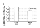
- FIG. 10 shows the results of simulating the size of the off-capacity external component CeX with respect to the semiconductor device 10 shown in FIG. 7 and the semiconductor device 12 according to the comparative example shown in FIG.
- FIG. 9 is a vertical cross-sectional view showing a cross-sectional configuration of the semiconductor device 12 according to the comparative example.
- the semiconductor device 12 according to the comparative example has the contact plugs 60S and 60D and the gate electrode 20 in the XY in-plane direction of the semiconductor layer 50 as compared with the semiconductor device 10 according to the present embodiment.
- the difference is that the second low dielectric constant region is not provided below the first low dielectric constant region 70 in the Z stacking direction of the semiconductor layer 50. That is, although the semiconductor device 12 according to the comparative example is provided with the same first low dielectric constant region 70 as compared with the semiconductor device 10 according to the present embodiment, the gate is in the XY in-plane direction of the semiconductor layer 50.
- the second low dielectric constant region 71 is not provided on both sides of the electrode 20.
- the simulation result of the external component CeX in the semiconductor device 10 according to the present embodiment is shown as an example, and the simulation result of the external component CeX in the semiconductor device 12 according to the comparative example is shown as a comparative example.
- the size of the external component Cex in the examples is smaller than the size of the external component Cex in the comparative example. Therefore, it can be seen that the semiconductor device 10 according to the present embodiment can further reduce the off capacitance by further providing the second low dielectric constant region 71.
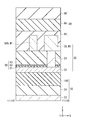
- the semiconductor device 10 shown in FIG. 7 has an insulating film 80 having at least one layer or more provided on the semiconductor layer 50 so as to cover the gate electrode 20, and the gate electrode 20 from the upper surface of the insulating film 80 having at least one layer or more. It is further provided with an opening P provided toward the upper surface of the.
- the opening P is provided in a plane region corresponding to the gate electrode 20 when at least one or more layers of the insulating film 80 are viewed in a plane from the stacking direction Z. Since the opening P is provided between the source electrode 30S and the drain electrode 30D, the opening width WP of the opening P is, for example, about 100 nm to 1000 nm.
- the first low dielectric constant region 70 is preferably provided inside such an opening P. Further, it is preferable that the second low dielectric constant region 71 is provided spatially continuously with the opening P and is provided spatially continuously with the first low dielectric constant region 70 provided inside the opening P. ..
- the first low dielectric constant region 70 and the second low dielectric constant region 71 may be provided so that the centers of the regions coincide with each other in either the X direction or the Y direction, and are provided in regions independent of each other. May be done.
- the insulating film 80 having at least one layer or more includes a plurality of insulating films formed of materials having different etching rates. According to this, in the insulating film 80 having at least one layer or more, the etching stop position of the opening P can be controlled with high accuracy in the manufacturing process described later by using the difference in the etching rate of each insulating film. It becomes.
- the insulating film 80 having at least one layer or more may be configured to include the first insulating film 81, the second insulating film 82, and the third insulating film 83.
- the first insulating film 81 is provided so as to cover the surface of the gate electrode 20 (that is, the upper surface and the side surface of the gate electrode 20) and the upper surface of the semiconductor layer 50.
- the second insulating film 82 is provided so as to cover the surface of the first insulating film 81.
- the second insulating film 82 is not provided on the surface of the first insulating film 81 provided on the surface of the gate electrode 20 (that is, the upper surface and the side surface of the gate electrode 20), and the first insulating film 81 is not provided. Is exposed with respect to the second low dielectric constant region 71. This is because, as will be described in the manufacturing process described later, in the semiconductor device 10, the second insulating film 82 is removed, so that the second low dielectric constant is formed between the first insulating film 81 and the third insulating film 83. This is because the rate region 71 is formed.
- the third insulating film 83 is provided between the surface of the second insulating film 82 and the lower surface of the first metal M1.
- the third insulating film 83 is provided so as to embed the gate electrode 20, and forms a second low dielectric constant region 71 with the first insulating film 81.
- the second insulating film 82 is preferably made of a material having an etching rate different from that of the material constituting the first insulating film 81 and the third insulating film 83.
- the second insulating film 82 is composed of a silicon nitride (SiN) film
- the first insulating film 81 and the third insulating film 83 are silicon oxide (SiO x ) having an etching rate different from that of silicon nitride (SiN). It is preferably composed of a film.
- the semiconductor device 10 by making the second insulating film 82 function as an etching stopper layer, an opening P that penetrates the third insulating film 83 and reaches the upper surface of the second insulating film 82 is easily formed. You will be able to do it. Further, the second low dielectric constant region 71 can be easily formed below the opening P by performing isotropic etching through the opening P and selectively removing the second insulating film 82. Will be.
- the insulating film 80 having at least one layer or more may be configured to further include the fourth insulating film 84.
- the fourth insulating film 84 may be provided so as to cover the upper surface of the third insulating film 83 and the surface of the first metal M1 (that is, the upper surface and the side surface of the first metal M1).
- the opening P is provided so as to penetrate the fourth insulating film 84 and the third insulating film 83 from the upper surface of the fourth insulating film 84.
- the fourth insulating film 84 may be composed of, for example, a silicon oxide (SiO x ) film.
- the insulating film 80 having at least one layer or more may be configured to further include the fifth insulating film 85.
- the fifth insulating film 85 may be provided on the fourth insulating film 84 and may close the upper part of the opening P.
- the fifth insulating film 85 may be composed of, for example, a silicon oxide (SiO x ) film.
- a sixth insulating film 86 made of, for example, a silicon oxide (SiO x ) film may be provided on the upper layer of the fifth insulating film 85, if necessary.
- a gap AG Air Gap
- the void AG of the first low dielectric constant region 70 is spatially continuously provided below the first low dielectric constant region 70 with the second low dielectric constant region 71 also formed as the void AG. May be good.
- the first low dielectric constant region 70 and the second low dielectric constant region 71 are lower than the silicon oxide (SiO x : relative permittivity 3.9) film constituting the third insulating film 83 and the fourth insulating film 84.
- the configuration inside the region is not particularly limited.
- the first low dielectric constant region 70 and the second low dielectric constant region 71 may be configured to contain air (relative permittivity 1.0) inside the gap AG so that the inside of the gap AG becomes a vacuum. It may be configured in.
- the first low dielectric constant region 70 and the second low dielectric constant region 71 may be formed by embedding a part or all of the inside of the void AG with a low dielectric constant material.
- the low dielectric constant material represents, for example, a dielectric material having a relative permittivity of 3 or less.
- the upper portion of the void AG is blocked by the fifth insulating film 85, so that the void AG becomes the fifth insulating film. It is hermetically sealed by 85.
- a part of the fifth insulating film 85 may enter the inside of the void AG. In such a case, the fifth insulating film 85 covers a part of the side surface or the bottom surface of the opening P.
- the width in which the first low dielectric constant region 70 and the second low dielectric constant region 71 are formed in the XY in-plane direction is not particularly limited.
- the width at which the first low dielectric constant region 70 is formed may be smaller than the width of the first insulating film 81 provided on the surface of the gate electrode 20 in one cross section cut in the stacking direction Z, for example.
- the width W70 of the first low dielectric constant region 70 may be smaller than the width W81 of the first insulating film 81 covering the upper surface and the side surface of the gate electrode 20.
- the width W70 of the first low dielectric constant region 70 covers the upper surface and the side surface of the gate electrode 20. It may be smaller than the width of the first insulating film 81 and the second insulating film 82. Further, when the first insulating film 81 is not formed on the upper surface and the side surface of the gate electrode 20, the width W70 of the first low dielectric constant region 70 may be smaller than the width of the gate electrode 20.
- the width at which the second low dielectric constant region 71 is formed may be larger than the width of the first insulating film 81 provided on the surface of the gate electrode 20 in one cross section cut in the stacking direction Z.
- the width W71 of the second low dielectric constant region 71 may be larger than the width W81 of the first insulating film 81 covering the upper surface and the side surface of the gate electrode 20 and smaller than the width between the contact plugs 60S and 60D. Good.
- the width W71 of the second low dielectric constant region 71 covers the upper surface and the side surface of the gate electrode 20. It may be larger than the width of the first insulating film 81 and the second insulating film 82. Further, when the first insulating film 81 is not formed on the upper surface and the side surface of the gate electrode 20, the width W71 of the second low dielectric constant region 71 may be larger than the width of the gate electrode 20.
- the multi-layer wiring unit 90 is provided with wiring for transmitting signals taken out from each electrode of the semiconductor device 10.
- FIG. 11 is a schematic view showing the positional relationship between the first low dielectric constant region 70 and the second low dielectric constant region 71 in the semiconductor device 10 shown in FIG. 7 and the multilayer wiring portion 90 in the Z stacking direction. ..
- the multilayer wiring unit 90 includes, for example, a first wiring layer 91 and a second wiring layer 92.
- the first wiring layer 91 is provided, for example, in the same layer as the first metal M1 including the source electrode 30S and the drain electrode 30D.
- the second wiring layer 92 is provided above the first wiring layer 91, and is connected to the first wiring layer 91 via, for example, a contact plug 93.
- the first low dielectric constant region 70 and the second low dielectric constant region 71 in the semiconductor device 10 are provided inside the element region AA1 of the active region AA activated by introducing conductive impurities into the semiconductor layer 50. ..
- the multilayer wiring portion 90 is provided inside the active region AA and inside the wiring region AA2 outside the element region AA1.
- the element region AA1 and the wiring region AA2 are separated from each other by, for example, an element separation layer 100 formed by the STI (Shallow Trench Isolation) method.
- the first low dielectric constant region 70 and the second low dielectric constant region 71 may not be provided between each of the first wiring layers 91 of the multilayer wiring portion 90 and between each of the second wiring layers 92. Good. That is, the first low dielectric constant region 70 and the second low dielectric constant region 71 are provided at least in the semiconductor device 10 in the element region AA1 in the active region AA.
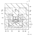
- FIG. 12 is a schematic view showing the positional relationship between the first low dielectric constant region 70 and the second low dielectric constant region 71 in the semiconductor device 10 shown in FIG. 7 and the multilayer wiring portion 90 in the XY in-plane direction. is there.
- a semiconductor device 10 As shown in FIG. 12, a semiconductor device 10, a first low dielectric constant region 70, and a second low dielectric constant region 71 are provided inside the active region AA.
- an element separation layer 100 formed by the STI method is provided over the entire surface, and a gate contact GC is provided.
- the active region AA is provided with the finger portion 21 of the gate electrode 20, the finger portion 31S of the source electrode 30S, and the finger portion 31D of the drain electrode 30D.
- the finger portion 21 of the gate electrode 20 is provided so as to extend in one direction (for example, the Y direction).
- the finger portion 31S of the source electrode 30S and the finger portion 31D of the drain electrode 30D are stretched in a direction parallel to the stretching direction of the finger portion 21 of the gate electrode 20 and are provided on both sides of the finger portion 21 of the gate electrode 20.
- the contact plugs 60S and 60D are stretched in a direction parallel to the stretching direction of the finger portion 21 of the gate electrode 20 and are provided below the finger portion 31S of the source electrode 30S and the finger portion 31D of the drain electrode 30D.
- the first low dielectric constant region 70 is stretched in a direction parallel to the stretching direction of the finger portion 21 of the gate electrode 20 and is provided on the finger portion 21 of the gate electrode 20. Further, the second low dielectric constant region 71 is stretched in a direction parallel to the stretching direction of the finger portion 21 of the gate electrode 20 and is provided on the side of the finger portion 21 of the gate electrode 20. That is, when the semiconductor layer 50 is viewed in a plan view from the Z stacking direction, the first low dielectric constant region 70 is provided in a region that overlaps with the finger portion 21 of the gate electrode 20 in the XY in-plane direction, and has a second low dielectric constant. Regions 71 are provided in regions on both sides of the finger portion 21 of the gate electrode 20 in the in-plane direction of the XY.
- the element separation region AB is provided with a connecting portion 22 of the gate electrode 20, a connecting portion 32S of the source electrode 30S, and a connecting portion 32D of the drain electrode 30D.
- the connecting portion 22 of the gate electrode 20 is connected to the gate contact GC. Further, the connecting portion 32S of the source electrode 30S is connected to a source contact (not shown), and the connecting portion 32D of the drain electrode 30D is connected to a drain contact (not shown).
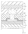
- FIG. 13 is a vertical cross-sectional view showing a cross-sectional structure taken along the line XV-XV of FIG. 14 is a vertical cross-sectional view showing the cross-sectional structure of the XVIA-XVIB line of FIG. 12
- FIG. 15 is a vertical cross-sectional view showing the cross-sectional structure of the XVIIB-XVIIC line of FIG. 12
- FIG. 16 is a vertical cross-sectional view of FIG. It is a vertical cross-sectional view which shows the cross-sectional structure in the XVIIIC-XVIIID line of.
- the connecting portion 22 of the gate electrode 20, the gate contact plug 24, and the gate contact layer 25 are sequentially provided on the element separation layer 100 formed by the STI method.
- the gate contact plug 24 has the same configuration as the contact plugs 60S and 60D, and is provided in the same layer as the contact plugs 60S and 60D.
- the gate contact layer 25 has the same configuration as the source electrode 30S and the drain electrode 30D, and is provided in the same layer as the first metal M1 including the source electrode 30S and the drain electrode 30D.
- the first low dielectric constant region 70 is preferably provided so as to avoid the gate contact GC. This is because when the first low dielectric constant region 70 is provided on the connecting portion 22 of the gate contact GC, it becomes difficult to provide the gate contact plug 24 on the connecting portion 22. Further, when the first low dielectric constant region 70 is not provided on the connecting portion 22 of the gate contact GC, the second low dielectric constant region 71 is also not provided. Further, the gate contact GC is preferably covered with at least one or more insulating films 80 (that is, the first insulating film 81 to the sixth insulating film 86), similarly to the gate electrode 20. According to this, since the gate contact GC can be protected by at least one or more layers of the insulating film 80 without exposing the gate contact GC, the reliability of the gate contact GC can be maintained.
- FIGS. 17 to 29 are vertical cross-sectional views showing each process of manufacturing the semiconductor device 10.
- an SOI substrate 55 in which an embedded oxide film 54 and a semiconductor layer 50 are laminated on a support substrate 53 is prepared.
- the element region AA1 is defined in the active region AA by forming the element separation layer 100 on the semiconductor layer 50 of the SOI substrate 55 using the STI method.
- the gate electrode 20 is formed on the semiconductor layer 50 via the gate insulating film 23.
- a second conductive type impurity for example, a p-type impurity such as boron (B) or aluminum (Al)
- B boron
- Al aluminum
- Well implantation and channel implantation are performed in the active region AA, and then the impurity membrane is removed.
- a thermal oxidation method for example, a gate insulating film 23 made of silicon oxide is formed with a thickness of about 5 nm to 15 nm.
- a gate electrode material film (not shown) made of polysilicon is formed on the semiconductor layer 50 and the gate insulating film 23 with a thickness of about 100 nm to 200 nm by using a CVD (Chemical Vapor Deposition) method. ..
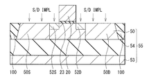
- the gate electrode 20 is formed on the upper surface of the semiconductor layer 50 by processing the formed gate electrode material film using photolithography and etching.
- the first conductive type impurities for example, n-type impurities such as arsenic (As) or phosphorus (P)
- the gate electrode 20 and an offset spacer are implanted using the gate electrode 20 and an offset spacer (not shown) as a mask.
- extension regions 52S and 52D are formed in the semiconductor layers 50 on both sides of the gate electrode 20.
- sidewalls are formed on both side surfaces of the gate electrode 20, and implantation S / D IMPL of the first conductive type impurity is performed again.
- the source region 50S and the drain region 50D can be formed on the semiconductor layers 50 on both sides of the gate electrode 20.
- the sidewall is removed after forming the source region 50S and the drain region 50D.
- a first insulating film 81 made of silicon oxide is formed on the surface of the gate electrode 20 and the upper surface of the semiconductor layer 50 with a thickness of about 10 nm to 100 nm by using, for example, a CVD method. To do.
- a second insulating film 82 made of silicon oxide forming the first insulating film 81 and silicon nitride having a different etching rate is formed on the surface of the first insulating film 81. It is formed with a thickness of about 10 nm to 100 nm.
- a third insulating film 83 made of silicon oxide is formed on the second insulating film 82 with a thickness of about 500 nm to 1500 nm.
- the third insulating film 83, the second insulating film 82, and the first insulating film 81 at positions corresponding to the source region 50S and the drain region 50D are used.
- the contact hole H1 that exposes the source region 50S and the drain region 50D is formed.
- the contact hole H1 is provided so as to extend in a direction parallel to the extending direction of the finger portion 21 of the gate electrode 20.
- an implantation Cnt IMPL of a high concentration of first conductive impurities (for example, n-type impurities such as arsenic (As) or phosphorus (P)) is sourced through the contact hole H1.
- first conductive impurities for example, n-type impurities such as arsenic (As) or phosphorus (P)
- the contact hole H1 By performing in the region 50S and the drain region 50D, the low resistance regions 51S and 51D are formed in the semiconductor layer 50.
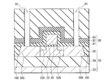
- the contact plugs 60S and 60D having a laminated structure are formed by laminating the titanium layer, the titanium nitride layer, and the tungsten layer in order in the contact hole H1.
- the contact plugs 60S and 60D can be electrically connected to the source region 50S and the drain region 50D via the low resistance regions 51S and 51D.
- the contact plugs 60S and 60D are provided so as to be stretched in a direction parallel to the stretching direction of the finger portion 21 of the gate electrode 20.
- a source electrode 30S made of aluminum (Al) and a drain electrode 30D are formed as the first metal M1 on the contact plugs 60S and 60D.
- the finger portion 31S of the source electrode 30S and the finger portion 31D of the drain electrode 30D are provided so as to extend in a direction parallel to the extending direction of the finger portion 21 of the gate electrode 20.
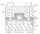
- the CVD method is used to form the fourth insulating film 84 made of silicon oxide on the upper surface of the third insulating film and the surface of the first metal M1.
- an opening P is formed which penetrates the fourth insulating film 84 and the third insulating film 83 and exposes the second insulating film 82.
- the resist 65 for forming a low dielectric constant region is patterned by using photolithography.
- the opening P is formed by removing a part of the fourth insulating film 84 and the third insulating film 83 by dry etching using the patterned low dielectric constant region forming resist 65 as a mask.
- the etching for forming the opening P is performed by dry etching having high anisotropy. By using such highly anisotropic etching, it is possible to form an opening P having a high aspect ratio in a desired region with high accuracy.
- the opening P is provided in the region between the first metal M1 in the XY in-plane direction of the semiconductor layer 50. Specifically, the opening P is provided in the region between the source electrode 30S and the drain electrode 30D (that is, above the gate electrode 20).
- the opening width WP of the opening P is, for example, about 100 nm to 1000 nm. Since the second insulating film 82 functions as an etching stopper in the formation of the opening P, the etching of the opening P proceeds to the fourth insulating film 84 made of silicon oxide and the third insulating film 83, and the second insulating film 82 Stop at the top surface.
- the void AG inside the opening P formed in this step becomes the first low dielectric constant region 70.
- a part of the second insulating film 82 is etched through the opening P with the resist 65 for forming the low dielectric constant region left, so that the first metal M1 is sandwiched between the first metal M1.
- a void AG continuous with the provided void AG is formed on the side of the gate electrode 20.
- the etching for removing a part of the second insulating film 82 is performed by using isotropic dry etching, wet etching, or the like. By using such isotropic etching, the second insulating film 82 provided on the upper surface and the side surface of the gate electrode 20 can be efficiently etched, and the void AG can be formed in a wider area.
- the void AG formed by removing the second insulating film 82 becomes the second low dielectric constant region 71. That is, since the void AG that becomes the first low dielectric constant region 70 is formed above the gate electrode 20, and the void AG that becomes the second low dielectric constant region 71 is formed on the side of the gate electrode 20, the semiconductor device 10 Can further reduce off-capacity external components.
- a CVD method under a condition of low embedding property in the void AG is used on the fourth insulating film 84.
- a fifth insulating film 85 made of silicon oxide is formed.
- the fifth insulating film 85 is deposited on the upper part of the opening P while overhanging. According to this, before the inside of the opening P is embedded with the fifth insulating film 85, the upper part of the opening P is closed with the fifth insulating film 85, so that the void sealed inside the opening P is airtightly sealed. AG is formed. At this time, the side surface of the opening P and the upper surface of the first insulating film 81 covering the gate electrode 20 may be covered with the fifth insulating film 85 that has entered the inside of the opening P.
- the first low dielectric constant region It functions as 70 and a second low dielectric constant region 71.
- the inside of the void AG may be a vacuum, and air (relative permittivity 1.0) may be present.
- the inside of the void AG is embedded with a material having a relative permittivity lower than that of silicon oxide (relative permittivity 3.9) forming the third insulating film 83, the fourth insulating film 84, and the fifth insulating film 85. It may be.
- the first low dielectric constant region 70 including at least one region between the first metal M1 in the in-plane direction of the XY and below the lower surface of the first metal M1 in the Z lamination method, and the XY plane.
- the second low dielectric constant region 71 including at least one region below the first low dielectric constant region 70 in the Z lamination method between the contact plugs 60S and 60D and the gate electrode 20 in the inward direction.
- a void AG will be provided in the region.
- the void AG in the first low dielectric constant region 70 and the void AG in the second low dielectric constant region 71 are formed spatially continuously.
- the sixth insulating film 86 is formed on the fifth insulating film 85 as needed, so that the semiconductor device 10 shown in FIG. 7 is formed.
- the second metal M2 and the second metal M2 are further formed by sequentially forming the metal layer and the insulating film on the fifth insulating film 85 in the same manner as the first metal M1 and the fourth insulating film 84. Can also form a third metal M3.
- the semiconductor device 10 is provided with the first low dielectric constant region 70 and the second low dielectric constant region 71 in the above-mentioned regions, so that the gate electrode 20, the contact plugs 60S, 60D, and the first It is possible to reduce the capacitance CgM between the one metal M1 and the capacitance CMM1 generated between the first metal M1. Therefore, the semiconductor device 10 can reduce the off-capacity external component CeX. According to this, since the semiconductor device 10 can reduce the product (Ron * Coff) of the on-resistance and the off-capacity, it is possible to promote the reduction of loss, which is an important characteristic of the high-frequency switch. ..
- the first low dielectric constant region 70 is further extended to a region between the lower surface and the upper surface of the first metal M1 in the Z stacking direction and a region above the upper surface of the first metal M1. May be provided.
- the semiconductor device 10 can further reduce the capacitance CgM between the gate electrode 20, the contact plugs 60S and 60D, and the first metal M1, and the capacitance CMM1 generated between the first metal M1. Will be.
- the semiconductor device 10 is configured by providing at least one or more insulating films 80 including insulating films formed of materials having different etching rates on the semiconductor layer 50. According to this, in the semiconductor device 10, the etching stop position of the opening P used for forming the first low dielectric constant region 70 and the second low dielectric constant region 71 is determined by using the difference in the etching rate of each insulating film. It is possible to control with high precision. Therefore, according to the present embodiment, the semiconductor device 10 can be manufactured more stably and with high reliability.
- the state of embedding the fifth insulating film 85 in the opening P shown in the vertical cross-sectional view of FIG. 7 and the like, and the state of covering the side surface of the opening P and the upper surface of the first insulating film 81 covering the gate electrode 20 are as follows. It is merely an example and does not limit the structure of the semiconductor device 10 according to the present embodiment.
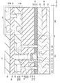
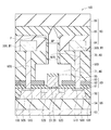
- FIG. 30 is a vertical cross-sectional view showing a cross-sectional configuration of the semiconductor device 10A according to the present embodiment.
- FIG. 30 shows the cross-sectional structure of the line VII-VII of FIG. 6, similarly to FIG. 7.
- the semiconductor device 10A expands the range of isotropic etching of the second insulating film 82 performed through the opening P with respect to the semiconductor device 10 shown in FIG.
- the difference is that the void AG that becomes the first low dielectric constant region 70 and the second low dielectric constant region 71 is enlarged by making the mixture.
- the semiconductor device 10A in addition to the second insulating film 82, the first insulating film 81 that covers the upper surface of the gate electrode 20, the third insulating film 83 on the side surface of the opening P, and the fourth insulating film 84 are provided. By removing it, the void AG can be formed in a wider range. According to this, the semiconductor device 10A has an off-capacity external component including a capacitance CgM between the gate electrode 20 and the contact plugs 60S, 60D or the first metal M1, and a capacitance CMM1 generated between the first metal M1. It is possible to further reduce Cex.
- the opening width WP of the opening P is expanded, the side surface and the bottom surface (that is, the upper surface of the gate electrode 20) of the opening P are thicker than the semiconductor device 10 shown in FIG.
- a fifth insulating film 85 having a thickness may be deposited.
- the fifth insulating film 85 deposited on the bottom surface of the opening P functions to protect the upper surface of the gate electrode 20 exposed inside the opening P by isotropic etching.
- the embedded state of the fifth insulating film 85 in the opening P shown in FIG. 30, the side surface of the opening P, and the coating state on the upper surface of the gate electrode 20 are merely examples. Therefore, the structure of the semiconductor device 10A according to the present embodiment is not limited.
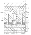
- FIG. 31 is a vertical cross-sectional view showing a cross-sectional configuration of the semiconductor device 10B according to the present embodiment.
- FIG. 31 shows the cross-sectional structure of the line VII-VII of FIG. 6, similarly to FIG. 7.
- the semiconductor device 10B according to the present embodiment has a second low dielectric constant while keeping the width W70 of the gap AG in the first low dielectric constant region 70 similar to that of the semiconductor device 10 shown in FIG.
- the gap AG in the region 71 can be expanded as compared with the semiconductor device 10A shown in FIG.
- the opening P having a narrower opening width WP is formed by making the opening width of the low dielectric constant region forming resist 65 used when forming the opening P narrower.
- the semiconductor device 10B expands the range of isotropic etching of the second insulating film 82 performed through the opening P, and covers the upper surface and the side surface of the gate electrode 20 in addition to the second insulating film 82.
- the void AG can be formed in a wider range.
- the opening width WP of the opening P widens before and after etching.
- the opening width WP of the opening P is excessively widened by etching to form the void AG, and the fifth insulating film is formed. It is possible to prevent the upper portion of the opening P from being difficult to be closed by the 85.
- isotropic etching for forming the void AG is performed by controlling the etching amount so that the semiconductor layer 50 is not exposed. Specifically, the isotropic etching for forming the void AG is performed by controlling the etching amount so that the first insulating film 81 provided on the upper surface of the semiconductor layer 50 does not disappear. This is because when the semiconductor layer 50 in the vicinity of the gate insulating film 23 is exposed or the gate insulating film 23 is side-etched, the variation in the gate length and the threshold voltage may become large.
- the semiconductor device 10B in addition to the second insulating film 82, the first insulating film 81 covering the upper surface and the side surface of the gate electrode 20, the third insulating film 83 on the side surface of the opening P, and the fourth insulating film 84 are removed. Therefore, the void AG can be formed in a wider range. According to this, the semiconductor device 10B has an off-capacity external component including a capacitance CgM between the gate electrode 20 and the contact plugs 60S, 60D or the first metal M1, a capacitance CMM1 generated between the first metal M1 and the like. It is possible to further reduce Cex.
- the opening width WP of the opening P is about the same as that of the semiconductor device 10 shown in FIG. 7, it is deposited on the side surface and the bottom surface (that is, the upper surface of the gate electrode 20) of the opening P.
- the film thickness of the fifth insulating film 85 can be reduced. According to this, the semiconductor device 10B can prevent the void AG that becomes the first low dielectric constant region 70 and the second low dielectric constant region 71 from being excessively embedded by the fifth insulating film 85. ..
- the embedded state of the fifth insulating film 85 in the opening P shown in FIG. 31, the side surface of the opening P, and the coating state on the upper surface of the gate electrode 20 are merely examples. Therefore, the structure of the semiconductor device 10B according to the present embodiment is not limited.
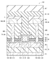
- FIG. 32 is a vertical cross-sectional view showing a cross-sectional configuration of the semiconductor device 10C according to the present embodiment.
- FIG. 32 shows the cross-sectional structure of the line VII-VII of FIG. 6, similarly to FIG. 7.
- the semiconductor device 10C according to the present embodiment has a first low dielectric constant by embedding a part of the opening P in the fifth insulating film 85 with respect to the semiconductor device 10 shown in FIG. The difference is that the rate region 70 and the second low dielectric constant region 71 are not spatially continuous and are isolated.
- the fifth insulating film 85 that closes the upper portion of the opening P when the fifth insulating film 85 that closes the upper portion of the opening P is formed, the fifth insulating film 85 is formed by a CVD method under conditions of high embedding property. More fifth insulating film 85 is deposited inside the opening P. As a result, the semiconductor device 10C couples the fifth insulating film 85 deposited on the side surface and the bottom surface (that is, the upper surface of the first insulating film 81) of the opening P, and the first low dielectric constant region 70 and the second The low dielectric constant region 71 can be separated from each other. As a result, the first low dielectric constant region 70 is provided above the gate electrode 20, and the second low dielectric constant region 71 is provided so as to surround the side surface of the gate electrode 20 so as to be separated from each other.
- the semiconductor device 10C has the gate electrode 20 and the contact plugs 60S, 60D or the first metal M1 as in the semiconductor device 10 shown in FIG. It is possible to reduce the off-capacity external component Cex including the capacitance CgM between and the capacitance CMM1 generated between the first metal M1.
- the embedded state of the fifth insulating film 85 in the opening P shown in FIG. 32, the side surface of the opening P, and the covering state of the upper surface of the first insulating film 81 are limited to the last. It is an example and does not limit the structure of the semiconductor device 10C according to the present embodiment.
- FIG. 33 is a vertical cross-sectional view showing a cross-sectional configuration of the semiconductor device 10D according to the present embodiment.
- FIG. 33 shows the cross-sectional structure of the line VII-VII of FIG. 6, similarly to FIG. 7.
- the opening P is embedded in the fifth insulating film 85 with respect to the semiconductor device 10 shown in FIG. 7, so that the first low dielectric constant region 70 The difference is that the region corresponding to is embedded in the fifth insulating film 85.
- the fifth insulating film 85 that closes the upper portion of the opening P is formed, the fifth insulating film 85 is formed by a CVD method under the condition that the opening P is highly embedded. As a result, the region from the upper surface of the first insulating film 81 of the opening P to the opening surface is embedded in the fifth insulating film 85. As a result, the opening P below the lower surface of the first metal M1 and above the upper surface of the first insulating film 81 is embedded with the fifth insulating film 85.
- the fifth insulating film 85 is first formed in the same manner as the semiconductor device 10 shown in FIG. It can function as a low dielectric constant region 70.
- the second low dielectric constant region 71 is composed of a void AG surrounding the side surface of the gate electrode 20.
- the semiconductor device 10D has the gate electrode 20 and the contact plugs 60S, 60D or the first metal M1 as in the semiconductor device 10 shown in FIG. It is possible to reduce the off-capacity external component Cex including the capacitance CgM between and the capacitance CMM1 generated between the first metal M1.
- the embedded state of the fifth insulating film 85 in the opening P shown in FIG. 33 is merely an example and limits the structure of the semiconductor device 10D according to the present embodiment. is not.
- FIG. 34 is a vertical cross-sectional view showing a cross-sectional configuration of the semiconductor device 10E according to the present embodiment.
- FIG. 34 shows the cross-sectional structure of the line VII-VII of FIG. 6, similarly to FIG. 7.
- the semiconductor device 10E according to the present embodiment is different in that the fifth insulating film 85 is formed by applying a fluid material to the semiconductor device 10D shown in FIG. 33.
- the fifth insulating film 85 is used by using SOG (Spin On Glass) which is a low-dielectric film, coating film formation of an organic resin film, or pasting film formation of an organic resin film.
- SOG Spin On Glass
- the upper part of the opening P is closed. Since the SOG and the organic resin have high fluidity, the region from the opening surface to the upper surface of the first insulating film 81 of the opening P can be easily embedded in the fifth insulating film 85 as compared with the CVD method.
- the opening P below the lower surface of the first metal M1 and above the upper surface of the first insulating film 81 is embedded with the fifth insulating film 85 made of SOG or an organic resin, which is a low dielectric film. Similar to the semiconductor device 10 shown in FIG. 7, it can function as the first low dielectric constant region 70. Further, the second low dielectric constant region 71 is composed of a void AG surrounding the side surface of the gate electrode 20.
- the semiconductor device 10E has the gate electrode 20 and the contact plugs 60S, 60D or the first metal M1 as in the semiconductor device 10 shown in FIG. It is possible to reduce the off-capacity external component Cex including the capacitance CgM between and the capacitance CMM1 generated between the first metal M1.
- the embedded state of the fifth insulating film 85 in the opening P shown in FIG. 34 is merely an example and limits the structure of the semiconductor device 10E according to the present embodiment. is not.
- FIG. 35 is a vertical cross-sectional view showing a cross-sectional configuration of the semiconductor device 10F according to the present embodiment.
- FIG. 35 shows the cross-sectional structure of the line VII-VII of FIG. 6, similarly to FIG. 7.
- the semiconductor device 10F has the second metal M2 provided between the fourth insulating film 84 and the fifth insulating film 85 with respect to the semiconductor device 10 shown in FIG. The difference is that the surface of the second metal M2 and the seventh insulating film 87 covering the upper surface of the fourth insulating film 84 are further provided.
- the fourth insulating film 84 is provided by embedding the first metal M1 and the contact plug 61 provided on the upper surface of the first metal M1. Further, a second metal M2 connected to the first metal M1 via the contact plug 61 is provided on the fourth insulating film 84, and the surface of the second metal M2 and the upper surface of the fourth insulating film are formed on the surface of the second metal M2. A seventh insulating film 87 is provided. The opening P is formed from the upper surface of the seventh insulating film 87, and the upper portion is closed by the fifth insulating film 85 provided on the seventh insulating film 87.
- the materials constituting the second metal M2, the seventh insulating film 87, and the contact plug 61 are substantially the same as those of the first metal M1, the fourth insulating film 84, and the contact plugs 60S and 60D, respectively. The description of is omitted.
- the first low dielectric constant region 70 made of the void AG can be extended between the second metal M2 provided on the first metal M1.
- the semiconductor device 10F is provided with the gate electrode 20 in addition to the capacitance CgM between the gate electrode 20 and the contact plugs 60S, 60D or the first metal M1 and the capacitance CMM1 generated between the first metal M1. It is possible to reduce the capacitance Cg between the second metal M2 and the capacitance CMM2 generated between the second metal M2. Therefore, the semiconductor device 10F can reduce the off-capacity external component Cex including these capacitances.
- the embedded state of the fifth insulating film 85 in the opening P shown in FIG. 35, the side surface of the opening P, and the covering state of the upper surface of the first insulating film 81 are limited to the last. It is an example and does not limit the structure of the semiconductor device 10F according to the present embodiment.
- FIG. 36 is a schematic view showing an example of the configuration of the wireless communication device.
- the wireless communication device 3 includes, for example, an antenna ANT, a high frequency switch 1, a high power amplifier HPA, a high frequency integrated circuit RFIC (Radio Frequency Integrated Circuit), a base band portion BB, and audio output.
- a unit MIC, a data output unit DT, and an interface unit I / F are provided.
- the wireless communication device 3 is a high-frequency module used in a mobile phone system having multiple functions such as voice, data communication, and LAN (Local Area Network) connection.
- the high frequency switch 1 includes any of the semiconductor devices 10, 10A to 10F according to the first to seventh embodiments.
- the wireless communication device 3 When the transmission signal is output from the transmission system of the wireless communication device 3 to the antenna ANT (that is, at the time of transmission), the wireless communication device 3 outputs the transmission signal output from the baseband portion BB to the high frequency integrated circuit RFIC and the high power amplifier HPA. , And output to the antenna ANT via the high frequency switch 1.
- the wireless communication device 3 transmits the received signal via the high frequency switch 1 and the high frequency integrated circuit RFIC. Input to the baseband section BB.
- the received signal processed by the baseband unit BB is output from an output unit such as an audio output unit MIC, a data output unit DT, or an interface unit I / F.
- the first conductive type impurity is an n-type impurity such as arsenic (As) or phosphorus (P), and the second conductive type impurity is boron (B), aluminum (Al) or the like.
- the first conductive type impurity is a p-type impurity such as boron (B) or aluminum (Al)
- the second conductive type impurity is an n-type impurity such as arsenic (As) or phosphorus (P). You may.
- the configurations of the high-frequency switch 1, the semiconductor device 10 such as the field-effect transistor, and the wireless communication device 3 have been specifically described as embodiments of the technology according to the present disclosure.
- the present invention is not limited to those including all of the illustrated components, and it is possible to replace some of the components with other components.
- the semiconductor device 10 includes a high frequency switch (RF-SW), a PA (Power Amplifier), and the like. It can also be applied to other high frequency devices.
- RF-SW high frequency switch
- PA Power Amplifier
- each layer described in the above embodiment, the film forming method, and the like are not limited to the above, and may be another shape, material, and thickness, or another film forming method. May be.
- the terms used in this specification include those used only for convenience of explanation and not limiting the configuration and operation.
- the terms “right”, “left”, “top”, and “bottom” only indicate the direction on the referenced drawing.
- the terms “inside” and “outside” indicate a direction toward the center of the attention element and a direction away from the center of the attention element, respectively. The same applies to terms similar to these and terms having a similar purpose.
- the technology according to the present disclosure can also have the following configuration. According to the technique according to the present disclosure having the following configuration, the off capacitance of the field effect transistor can be reduced.
- the effects exerted by the techniques according to the present disclosure are not necessarily limited to the effects described herein, and may be any of the effects described in the present disclosure.
- the semiconductor device according to any one of (1) to (3), wherein the second low dielectric constant region is continuously provided with the first low dielectric constant region.
- the first low dielectric constant region and the second low dielectric constant region each include voids.
- the semiconductor device according to (4), wherein the voids included in the first low dielectric constant region and the voids included in the second low dielectric constant region are continuously provided.
- the semiconductor device according to any one of (1) to (5) above, wherein the first low dielectric constant region is provided inside the opening.
- the insulating film having one or more layers is A first insulating film covering the surface of the gate electrode and the surface of the semiconductor layer, A second insulating film that covers the surface of the first insulating film and It includes a third insulating film provided between the surface of the second insulating film and the lower surface of the first metal.
- the first insulating film is formed of a material having an etching rate different from that of the second insulating film.
- the one or more layers of the insulating film further include a fourth insulating film that covers the upper surface of the third insulating film and the surface of the first metal.
- the one or more layers of the insulating film further include a fifth insulating film provided on the fourth insulating film.
- a second metal provided between the fourth insulating film and the fifth insulating film is further provided.
- the one or more layers of the insulating film further include a seventh insulating film that covers the upper surface of the fourth insulating film and the surface of the second metal.
- the fifth insulating film is made of a material having a dielectric constant lower than that of the third insulating film and the material forming the fourth insulating film.
- the insulating film having one or more layers is A first insulating film covering the surface of the gate electrode and the surface of the semiconductor layer, A second insulating film that covers the surface of the first insulating film and A third insulating film provided between the surface of the second insulating film and the lower surface of the first metal, and A fourth insulating film that covers the upper surface of the third insulating film and the surface of the first metal, A fifth insulating film provided on the fourth insulating film and closing the opening is included.
- the second low dielectric constant region includes voids provided in a region where at least one of the first insulating film, the second insulating film, or the third insulating film is formed in the stacking direction.
- the fifth insulating film is made of a material having a dielectric constant lower than that of the third insulating film and the material forming the fourth insulating film.
- the second low dielectric constant region includes a region embedded in the fifth insulating film.
- the gate electrode is provided so as to extend in one direction in the in-plane direction.
- the contact plug, the first metal, the first low dielectric constant region, and the second low dielectric constant region are provided so as to be stretched in the in-plane direction in a direction parallel to the stretching direction of the gate electrode.
- the semiconductor device according to any one of (1) to (24).
- (26) The semiconductor device according to (25), wherein the first low dielectric constant region and the second low dielectric constant region are stretched in the in-plane direction in a direction intersecting the stretching direction of the gate electrode. ..
- the gate electrode includes a plurality of finger portions extended in the same direction and a connecting portion for connecting the plurality of finger portions.
- the first low dielectric constant region is provided above the finger portion or above at least a part of the connecting portion.
- (28) In the in-plane direction The source region, the element region including the drain region, and A wiring region having a multi-layer wiring portion and being partitioned from the element region by an element separation layer, Is provided,
Landscapes
- Electrodes Of Semiconductors (AREA)
- Insulated Gate Type Field-Effect Transistor (AREA)
- Internal Circuitry In Semiconductor Integrated Circuit Devices (AREA)
- Thin Film Transistor (AREA)
- Metal-Oxide And Bipolar Metal-Oxide Semiconductor Integrated Circuits (AREA)
- Engineering & Computer Science (AREA)
- Manufacturing & Machinery (AREA)
Abstract
Description
1.第1の実施形態
1.1.高周波スイッチの構成
1.2.半導体装置の構成
1.3.半導体装置の製造方法
2.第2の実施形態
3.第3の実施形態
4.第4の実施形態
5.第5の実施形態
6.第6の実施形態
7.第7の実施形態
8.適用例
(1.1.高周波スイッチの構成)
まず、図1~図5を参照して、本開示の第1の実施形態に係る半導体装置を含む高周波スイッチの構成について説明する。図1は、入出力ポート数が1対10である高周波スイッチの構成を示した模式図であり、図2は、入出力ポート数が1対1である高周波スイッチの構成を示した模式図である。
次に、図6及び図7を参照して、本開示の第1の実施形態に係る半導体装置の構成について説明する。図6は、本実施形態に係る半導体装置の全体構成を示す平面図である。
続いて、図17~図29を参照して、本実施形態に係る半導体装置10の製造方法について説明する。図17~図29は、半導体装置10を製造する各工程を示した縦断面図である。
次に、図30を参照して、本開示の第2の実施形態に係る半導体装置の構成について説明する。図30は、本実施形態に係る半導体装置10Aの断面構成を示す縦断面図である。図30は、図7と同様に、図6のVII-VII線における断面構成を示す。
続いて、図31を参照して、本開示の第3の実施形態に係る半導体装置の構成について説明する。図31は、本実施形態に係る半導体装置10Bの断面構成を示す縦断面図である。図31は、図7と同様に、図6のVII-VII線における断面構成を示す。
次に、図32を参照して、本開示の第4の実施形態に係る半導体装置の構成について説明する。図32は、本実施形態に係る半導体装置10Cの断面構成を示す縦断面図である。図32は、図7と同様に、図6のVII-VII線における断面構成を示す。
続いて、図33を参照して、本開示の第5の実施形態に係る半導体装置の構成について説明する。図33は、本実施形態に係る半導体装置10Dの断面構成を示す縦断面図である。図33は、図7と同様に、図6のVII-VII線における断面構成を示す。
次に、図34を参照して、本開示の第6の実施形態に係る半導体装置の構成について説明する。図34は、本実施形態に係る半導体装置10Eの断面構成を示す縦断面図である。図34は、図7と同様に、図6のVII-VII線における断面構成を示す。
続いて、図35を参照して、本開示の第7の実施形態に係る半導体装置の構成について説明する。図35は、本実施形態に係る半導体装置10Fの断面構成を示す縦断面図である。図35は、図7と同様に、図6のVII-VII線における断面構成を示す。
さらに、図36を参照して、本開示の第1~第7の実施形態に係る半導体装置の適用例である無線通信装置の構成について説明する。図36は、無線通信装置の構成の一例を示す模式図である。
(1)
ゲート電極と、
前記ゲート電極を間にしてソース領域、及びドレイン領域を有する半導体層と、
前記ソース領域、及び前記ドレイン領域の上にそれぞれ設けられたコンタクトプラグと、
前記コンタクトプラグの各々の上に積層された第1メタルと、
前記半導体層の面内方向において前記第1メタルの各々の間、かつ前記半導体層の積層方向において前記第1メタルの下面よりも下方の少なくともいずれかの領域に設けられた第1低誘電率領域と、
前記面内方向において前記コンタクトプラグと前記ゲート電極との間、かつ前記積層方向において前記第1低誘電率領域よりも下方の少なくともいずれかの領域に設けられた第2低誘電率領域と
を備え、
前記第2低誘電率領域は、前記第1低誘電率領域が設けられる平面領域とは少なくとも一部が異なる平面領域に設けられる、半導体装置。
(2)
前記第1低誘電率領域は、前記積層方向において前記第1メタルの上面と下面との間の少なくともいずれかの領域にさらに延伸して設けられる、前記(1)に記載の半導体装置。
(3)
前記第1低誘電率領域は、前記積層方向において前記第1メタルの上面よりも上方の少なくともいずれかの領域にさらに延伸して設けられる、前記(2)に記載の半導体装置。
(4)
前記第2低誘電率領域は、前記第1低誘電率領域と連続して設けられる、前記(1)~(3)のいずれか一項に記載の半導体装置。
(5)
前記第1低誘電率領域、及び前記第2低誘電率領域は、それぞれ空隙を含み、
前記第1低誘電率領域に含まれる空隙と、前記第2低誘電率領域に含まれる空隙とは連続して設けられる、前記(4)に記載の半導体装置。
(6)
前記ゲート電極を覆うように前記半導体層の上に設けられた1層以上の絶縁膜と、
前記1層以上の絶縁膜の上面から、前記ゲート電極に対応する平面領域に設けられた開口と
をさらに備え、
前記第1低誘電率領域は、前記開口の内部に設けられる、前記(1)~(5)のいずれか一項に記載の半導体装置。
(7)
前記1層以上の絶縁膜は、エッチングレートが異なる材料でそれぞれ形成された絶縁膜を含む、前記(6)に記載の半導体装置。
(8)
前記1層以上の絶縁膜は、
前記ゲート電極の表面、及び前記半導体層の表面を覆う第1絶縁膜と、
前記第1絶縁膜の表面を覆う第2絶縁膜と、
前記第2絶縁膜の表面と前記第1メタルの下面との間に設けられた第3絶縁膜と
を含み、
前記第1絶縁膜は、前記第2絶縁膜の材料とは異なるエッチングレートの材料で形成される、前記(7)に記載の半導体装置。
(9)
前記積層方向の一断面において、前記第1低誘電率領域の幅は、前記ゲート電極の表面に設けられた前記第1絶縁膜の幅よりも小さい、前記(8)に記載の半導体装置。
(10)
前記開口は、前記ゲート電極の上の前記第3絶縁膜を少なくとも貫通して設けられる、前記(8)又は(9)に記載の半導体装置。
(11)
前記開口は、前記ゲート電極の上の前記第2絶縁膜、又は前記第2絶縁膜及び前記第1絶縁膜をさらに貫通して設けられる、前記(10)に記載の半導体装置。
(12)
前記1層以上の絶縁膜は、前記第3絶縁膜の上面、及び前記第1メタルの表面を覆う第4絶縁膜をさらに含み、
前記開口は、前記第4絶縁膜の上面から設けられる、前記(10)又は(11)に記載の半導体装置。
(13)
前記1層以上の絶縁膜は、前記第4絶縁膜の上に設けられた第5絶縁膜をさらに含み、
前記第5絶縁膜は、前記開口の上部を閉塞する、前記(12)に記載の半導体装置。
(14)
前記第4絶縁膜と前記第5絶縁膜との間に設けられた第2メタルをさらに備え、
前記1層以上の絶縁膜は、前記第4絶縁膜の上面、及び前記第2メタルの表面を覆う第7絶縁膜をさらに含み、
前記開口は、前記第7絶縁膜の上面から設けられる、前記(13)に記載の半導体装置。
(15)
前記第5絶縁膜は、前記開口の側面の少なくとも一部を被覆する、前記(13)又は(14)に記載の半導体装置。
(16)
前記第5絶縁膜は、前記第3絶縁膜、及び前記第4絶縁膜を形成する材料よりも誘電率が低い材料にて形成されており、
前記第1低誘電率領域は、前記第5絶縁膜にて埋め込まれた前記開口の少なくとも一部を含む、前記(13)~(15)のいずれか一項に記載の半導体装置。
(17)
前記1層以上の絶縁膜は、
前記ゲート電極の表面、及び前記半導体層の表面を覆う第1絶縁膜と、
前記第1絶縁膜の表面を覆う第2絶縁膜と、
前記第2絶縁膜の表面と前記第1メタルの下面との間に設けられた第3絶縁膜と、
前記第3絶縁膜の上面、及び前記第1メタルの表面を覆う第4絶縁膜と、
前記第4絶縁膜の上に設けられ、前記開口を閉塞する第5絶縁膜と
を含み、
前記第2低誘電率領域は、前記積層方向において、前記第1絶縁膜、前記第2絶縁膜、又は前記第3絶縁膜の少なくともいずれかが形成された領域に設けられた空隙を含む、前記(6)に記載の半導体装置。
(18)
前記第2低誘電率領域に含まれる空隙は、前記第1絶縁膜の少なくとも一部を露出させる、前記(17)に記載の半導体装置。
(19)
前記第2低誘電率領域に含まれる空隙は、前記半導体層の表面に設けられた前記第1絶縁膜を露出させる、前記(18)に記載の半導体装置。
(20)
前記第2低誘電率領域に含まれる空隙は、前記ゲート電極の少なくとも一部をさらに露出させる、前記(19)に記載の半導体装置。
(21)
前記第2低誘電率領域に含まれる空隙は、前記第4絶縁膜の上面から前記ゲート電極の上の前記第3絶縁膜を少なくとも貫通して設けられる前記開口と連続して設けられる、前記(17)~(20)のいずれか一項に記載の半導体装置。
(22)
前記第5絶縁膜は、前記第2低誘電率領域に含まれる空隙の側面、又は底面の少なくとも一部を被覆する、前記(21)に記載の半導体装置。
(23)
前記積層方向の一断面において、前記第2低誘電率領域が設けられた領域の幅は、前記ゲート電極の表面に設けられた前記第1絶縁膜の幅よりも大きい、前記(17)~(22)のいずれか一項に記載の半導体装置。
(24)
前記第5絶縁膜は、前記第3絶縁膜、及び前記第4絶縁膜を形成する材料よりも誘電率が低い材料にて形成されており、
前記第2低誘電率領域は、前記第5絶縁膜にて埋め込まれた領域を含む、前記(17)~(23)のいずれか一項に記載の半導体装置。
(25)
前記ゲート電極は、前記面内方向に一方向に延伸されて設けられ、
前記コンタクトプラグ、前記第1メタル、前記第1低誘電率領域、及び前記第2低誘電率領域は、前記面内方向において、前記ゲート電極の延伸方向と平行方向に延伸されて設けられる、前記(1)~(24)のいずれか一項に記載の半導体装置。
(26)
前記第1低誘電率領域、及び前記第2低誘電率領域は、前記面内方向において、前記ゲート電極の延伸方向と交差する方向に延伸されて設けられる、前記(25)に記載の半導体装置。
(27)
前記ゲート電極は、同一方向に延伸された複数のフィンガー部と、前記複数のフィンガー部を連結する連結部とを含み、
前記第1低誘電率領域は、前記フィンガー部の上方、又は前記連結部の少なくとも一部の上方に設けられ、
前記第2低誘電率領域は、前記フィンガー部の側壁、又は前記連結部の少なくとも一部の側壁に設けられる、前記(1)~(26)のいずれか一項に記載の半導体装置。
(28)
前記面内方向において、
前記ソース領域、及び前記ドレイン領域を含む素子領域と、
多層配線部を有し、素子分離層によって前記素子領域と区画される配線領域と、
が設けられ、
前記第1低誘電率領域、及び前記第2低誘電率領域は、前記素子領域内に設けられる、前記(1)~(27)のいずれか一項請求項1に記載の半導体装置。
(29)
前記面内方向において、
前記素子領域、及び前記配線領域を含むアクティブ領域と、
前記素子分離層を含み、前記アクティブ領域の外側に設けられた素子分離領域と、
が設けられ、
前記素子分離領域の前記素子分離層の上には、前記ゲート電極と接続されたゲートコンタクトが設けられ、
前記第1低誘電率領域、及び前記第2低誘電率領域は、前記ゲートコンタクトを回避して設けられる、前記(28)に記載の半導体装置。
(30)
高周波デバイス用の電界効果トランジスタとして用いられる、前記(1)~(29)のいずれか一項に記載の半導体装置。
(31)
半導体層の上面側にゲート電極を形成する工程と、
前記半導体層に、前記ゲート電極を間にしてソース領域、及びドレイン領域を形成する工程と、
前記ソース領域、及び前記ドレイン領域の各々の上にコンタクトプラグを形成する工程と、
前記コンタクトプラグの各々の上に第1メタルを積層する工程と、
前記半導体層の面内方向において前記第1メタルの各々の間、かつ前記半導体層の積層方向において前記第1メタルの下面よりも下方の少なくともいずれかの領域に第1低誘電率領域を形成する工程と、
前記面内方向において前記コンタクトプラグと前記ゲート電極との間、かつ前記積層方向において前記第1低誘電率領域よりも下方の少なくともいずれかの領域に第2低誘電率領域を形成する工程と
を含み、
前記第1低誘電率領域が形成される平面領域とは少なくとも一部が異なる平面領域に前記第2低誘電率領域を形成する、半導体装置の製造方法。
Claims (31)
- ゲート電極と、
前記ゲート電極を間にしてソース領域、及びドレイン領域を有する半導体層と、
前記ソース領域、及び前記ドレイン領域の上にそれぞれ設けられたコンタクトプラグと、
前記コンタクトプラグの各々の上に積層された第1メタルと、
前記半導体層の面内方向において前記第1メタルの各々の間、かつ前記半導体層の積層方向において前記第1メタルの下面よりも下方の少なくともいずれかの領域に設けられた第1低誘電率領域と、
前記面内方向において前記コンタクトプラグと前記ゲート電極との間、かつ前記積層方向において前記第1低誘電率領域よりも下方の少なくともいずれかの領域に設けられた第2低誘電率領域と
を備え、
前記第2低誘電率領域は、前記第1低誘電率領域が設けられる平面領域とは少なくとも一部が異なる平面領域に設けられる、半導体装置。 - 前記第1低誘電率領域は、前記積層方向において前記第1メタルの上面と下面との間の少なくともいずれかの領域にさらに延伸して設けられる、請求項1に記載の半導体装置。
- 前記第1低誘電率領域は、前記積層方向において前記第1メタルの上面よりも上方の少なくともいずれかの領域にさらに延伸して設けられる、請求項2に記載の半導体装置。
- 前記第2低誘電率領域は、前記第1低誘電率領域と連続して設けられる、請求項1に記載の半導体装置。
- 前記第1低誘電率領域、及び前記第2低誘電率領域は、それぞれ空隙を含み、
前記第1低誘電率領域に含まれる空隙と、前記第2低誘電率領域に含まれる空隙とは連続して設けられる、請求項4に記載の半導体装置。 - 前記ゲート電極を覆うように前記半導体層の上に設けられた1層以上の絶縁膜と、
前記1層以上の絶縁膜の上面から、前記ゲート電極に対応する平面領域に設けられた開口と
をさらに備え、
前記第1低誘電率領域は、前記開口の内部に設けられる、請求項1に記載の半導体装置。 - 前記1層以上の絶縁膜は、エッチングレートが異なる材料でそれぞれ形成された絶縁膜を含む、請求項6に記載の半導体装置。
- 前記1層以上の絶縁膜は、
前記ゲート電極の表面、及び前記半導体層の表面を覆う第1絶縁膜と、
前記第1絶縁膜の表面を覆う第2絶縁膜と、
前記第2絶縁膜の表面と前記第1メタルの下面との間に設けられた第3絶縁膜と
を含み、
前記第1絶縁膜は、前記第2絶縁膜の材料とは異なるエッチングレートの材料で形成される、請求項7に記載の半導体装置。 - 前記積層方向の一断面において、前記第1低誘電率領域の幅は、前記ゲート電極の表面に設けられた前記第1絶縁膜の幅よりも小さい、請求項8に記載の半導体装置。
- 前記開口は、前記ゲート電極の上の前記第3絶縁膜を少なくとも貫通して設けられる、請求項8に記載の半導体装置。
- 前記開口は、前記ゲート電極の上の前記第2絶縁膜、又は前記第2絶縁膜及び前記第1絶縁膜をさらに貫通して設けられる、請求項10に記載の半導体装置。
- 前記1層以上の絶縁膜は、前記第3絶縁膜の上面、及び前記第1メタルの表面を覆う第4絶縁膜をさらに含み、
前記開口は、前記第4絶縁膜の上面から設けられる、請求項10に記載の半導体装置。 - 前記1層以上の絶縁膜は、前記第4絶縁膜の上に設けられた第5絶縁膜をさらに含み、
前記第5絶縁膜は、前記開口の上部を閉塞する、請求項12に記載の半導体装置。 - 前記第4絶縁膜と前記第5絶縁膜との間に設けられた第2メタルをさらに備え、
前記1層以上の絶縁膜は、前記第4絶縁膜の上面、及び前記第2メタルの表面を覆う第7絶縁膜をさらに含み、
前記開口は、前記第7絶縁膜の上面から設けられる、請求項13に記載の半導体装置。 - 前記第5絶縁膜は、前記開口の側面の少なくとも一部を被覆する、請求項13に記載の半導体装置。
- 前記第5絶縁膜は、前記第3絶縁膜、及び前記第4絶縁膜を形成する材料よりも誘電率が低い材料にて形成されており、
前記第1低誘電率領域は、前記第5絶縁膜にて埋め込まれた前記開口の少なくとも一部を含む、請求項13に記載の半導体装置。 - 前記1層以上の絶縁膜は、
前記ゲート電極の表面、及び前記半導体層の表面を覆う第1絶縁膜と、
前記第1絶縁膜の表面を覆う第2絶縁膜と、
前記第2絶縁膜の表面と前記第1メタルの下面との間に設けられた第3絶縁膜と、
前記第3絶縁膜の上面、及び前記第1メタルの表面を覆う第4絶縁膜と、
前記第4絶縁膜の上に設けられ、前記開口を閉塞する第5絶縁膜と
を含み、
前記第2低誘電率領域は、前記積層方向において、前記第1絶縁膜、前記第2絶縁膜、又は前記第3絶縁膜の少なくともいずれかが形成された領域に設けられた空隙を含む、請求項6に記載の半導体装置。 - 前記第2低誘電率領域に含まれる空隙は、前記第1絶縁膜の少なくとも一部を露出させる、請求項17に記載の半導体装置。
- 前記第2低誘電率領域に含まれる空隙は、前記半導体層の表面に設けられた前記第1絶縁膜を露出させる、請求項18に記載の半導体装置。
- 前記第2低誘電率領域に含まれる空隙は、前記ゲート電極の少なくとも一部をさらに露出させる、請求項19に記載の半導体装置。
- 前記第2低誘電率領域に含まれる空隙は、前記第4絶縁膜の上面から前記ゲート電極の上の前記第3絶縁膜を少なくとも貫通して設けられる前記開口と連続して設けられる、請求項17に記載の半導体装置。
- 前記第5絶縁膜は、前記第2低誘電率領域に含まれる空隙の側面、又は底面の少なくとも一部を被覆する、請求項21に記載の半導体装置。
- 前記積層方向の一断面において、前記第2低誘電率領域が設けられた領域の幅は、前記ゲート電極の表面に設けられた前記第1絶縁膜の幅よりも大きい、請求項17に記載の半導体装置。
- 前記第5絶縁膜は、前記第3絶縁膜、及び前記第4絶縁膜を形成する材料よりも誘電率が低い材料にて形成されており、
前記第2低誘電率領域は、前記第5絶縁膜にて埋め込まれた領域を含む、請求項17に記載の半導体装置。 - 前記ゲート電極は、前記面内方向に一方向に延伸されて設けられ、
前記コンタクトプラグ、前記第1メタル、前記第1低誘電率領域、及び前記第2低誘電率領域は、前記面内方向において、前記ゲート電極の延伸方向と平行方向に延伸されて設けられる、請求項1に記載の半導体装置。 - 前記第1低誘電率領域、及び前記第2低誘電率領域は、前記面内方向において、前記ゲート電極の延伸方向と交差する方向に延伸されて設けられる、請求項25に記載の半導体装置。
- 前記ゲート電極は、同一方向に延伸された複数のフィンガー部と、前記複数のフィンガー部を連結する連結部とを含み、
前記第1低誘電率領域は、前記フィンガー部の上方、又は前記連結部の少なくとも一部の上方に設けられ、
前記第2低誘電率領域は、前記フィンガー部の側壁、又は前記連結部の少なくとも一部の側壁に設けられる、請求項1に記載の半導体装置。 - 前記面内方向において、
前記ソース領域、及び前記ドレイン領域を含む素子領域と、
多層配線部を有し、素子分離層によって前記素子領域と区画される配線領域と、
が設けられ、
前記第1低誘電率領域、及び前記第2低誘電率領域は、前記素子領域内に設けられる、請求項1に記載の半導体装置。 - 前記面内方向において、
前記素子領域、及び前記配線領域を含むアクティブ領域と、
前記素子分離層を含み、前記アクティブ領域の外側に設けられた素子分離領域と、
が設けられ、
前記素子分離領域の前記素子分離層の上には、前記ゲート電極と接続されたゲートコンタクトが設けられ、
前記第1低誘電率領域、及び前記第2低誘電率領域は、前記ゲートコンタクトを回避して設けられる、請求項28に記載の半導体装置。 - 高周波デバイス用の電界効果トランジスタとして用いられる、請求項1に記載の半導体装置。
- 半導体層の上面側にゲート電極を形成する工程と、
前記半導体層に、前記ゲート電極を間にしてソース領域、及びドレイン領域を形成する工程と、
前記ソース領域、及び前記ドレイン領域の各々の上にコンタクトプラグを形成する工程と、
前記コンタクトプラグの各々の上に第1メタルを積層する工程と、
前記半導体層の面内方向において前記第1メタルの各々の間、かつ前記半導体層の積層方向において前記第1メタルの下面よりも下方の少なくともいずれかの領域に第1低誘電率領域を形成する工程と、
前記面内方向において前記コンタクトプラグと前記ゲート電極との間、かつ前記積層方向において前記第1低誘電率領域よりも下方の少なくともいずれかの領域に第2低誘電率領域を形成する工程と
を含み、
前記第1低誘電率領域が形成される平面領域とは少なくとも一部が異なる平面領域に前記第2低誘電率領域を形成する、半導体装置の製造方法。
Priority Applications (4)
| Application Number | Priority Date | Filing Date | Title |
|---|---|---|---|
| US17/618,656 US20220359706A1 (en) | 2019-06-20 | 2020-06-09 | Semiconductor device and method of manufacturing semiconductor device |
| JP2021528124A JP7568621B2 (ja) | 2019-06-20 | 2020-06-09 | 半導体装置、及び半導体装置の製造方法 |
| CN202080042916.7A CN114026688A (zh) | 2019-06-20 | 2020-06-09 | 半导体器件及半导体器件的制造方法 |
| DE112020002933.6T DE112020002933B4 (de) | 2019-06-20 | 2020-06-09 | Halbleitervorrichtung und Verfahren zum Herstellen einer Halbleitervorrichtung |
Applications Claiming Priority (2)
| Application Number | Priority Date | Filing Date | Title |
|---|---|---|---|
| JP2019-114339 | 2019-06-20 | ||
| JP2019114339 | 2019-06-20 |
Publications (1)
| Publication Number | Publication Date |
|---|---|
| WO2020255805A1 true WO2020255805A1 (ja) | 2020-12-24 |
Family
ID=74040785
Family Applications (1)
| Application Number | Title | Priority Date | Filing Date |
|---|---|---|---|
| PCT/JP2020/022738 Ceased WO2020255805A1 (ja) | 2019-06-20 | 2020-06-09 | 半導体装置、及び半導体装置の製造方法 |
Country Status (6)
| Country | Link |
|---|---|
| US (1) | US20220359706A1 (ja) |
| JP (1) | JP7568621B2 (ja) |
| CN (1) | CN114026688A (ja) |
| DE (1) | DE112020002933B4 (ja) |
| TW (1) | TWI890676B (ja) |
| WO (1) | WO2020255805A1 (ja) |
Families Citing this family (2)
| Publication number | Priority date | Publication date | Assignee | Title |
|---|---|---|---|---|
| US12500119B2 (en) | 2022-06-21 | 2025-12-16 | Globalfoundries Singapore Pte. Ltd. | Air gap with inverted T-shaped lower portion extending through at least one metal layer, and related method |
| CN119965155A (zh) * | 2025-01-26 | 2025-05-09 | 上海华虹宏力半导体制造有限公司 | 一种半导体器件及其制造方法 |
Citations (4)
| Publication number | Priority date | Publication date | Assignee | Title |
|---|---|---|---|---|
| JPH09283757A (ja) * | 1996-04-19 | 1997-10-31 | Hitachi Ltd | 電界効果トランジスタおよびその製造方法ならびに半導体集積回路装置およびその製造方法 |
| JP2001111051A (ja) * | 1999-10-13 | 2001-04-20 | Sony Corp | 半導体装置及びその製造方法 |
| JP2002359369A (ja) * | 2001-06-01 | 2002-12-13 | Sony Corp | 半導体装置の製造方法 |
| JP2015207640A (ja) * | 2014-04-18 | 2015-11-19 | ソニー株式会社 | 電界効果トランジスタおよびその製造方法 |
Family Cites Families (8)
| Publication number | Priority date | Publication date | Assignee | Title |
|---|---|---|---|---|
| JP4572054B2 (ja) * | 2002-01-24 | 2010-10-27 | 寛治 大塚 | 回路構造及び半導体集積回路 |
| US8232618B2 (en) * | 2010-08-11 | 2012-07-31 | International Business Machines Corporation | Semiconductor structure having a contact-level air gap within the interlayer dielectrics above a semiconductor device and a method of forming the semiconductor structure using a self-assembly approach |
| CN103050540B (zh) * | 2012-12-20 | 2016-03-30 | 电子科技大学 | 使用高介电常数槽结构的低比导通电阻的横向功率器件 |
| US10211146B2 (en) * | 2016-05-12 | 2019-02-19 | Globalfoundries Inc. | Air gap over transistor gate and related method |
| US10157777B2 (en) * | 2016-05-12 | 2018-12-18 | Globalfoundries Inc. | Air gap over transistor gate and related method |
| US10157778B2 (en) * | 2016-05-31 | 2018-12-18 | Taiwan Semiconductor Manufacturing Co., Ltd. | Semiconductor structure and manufacturing method thereof |
| US20180366553A1 (en) * | 2017-06-15 | 2018-12-20 | Globalfoundries Inc. | Methods of forming an air gap adjacent a gate structure of a finfet device and the resulting devices |
| JP7027874B2 (ja) | 2017-12-21 | 2022-03-02 | トヨタ自動車株式会社 | 燃料電池用セパレータ及びその製造方法 |
-
2020
- 2020-04-17 TW TW109112926A patent/TWI890676B/zh active
- 2020-06-09 CN CN202080042916.7A patent/CN114026688A/zh active Pending
- 2020-06-09 DE DE112020002933.6T patent/DE112020002933B4/de active Active
- 2020-06-09 WO PCT/JP2020/022738 patent/WO2020255805A1/ja not_active Ceased
- 2020-06-09 JP JP2021528124A patent/JP7568621B2/ja active Active
- 2020-06-09 US US17/618,656 patent/US20220359706A1/en not_active Abandoned
Patent Citations (4)
| Publication number | Priority date | Publication date | Assignee | Title |
|---|---|---|---|---|
| JPH09283757A (ja) * | 1996-04-19 | 1997-10-31 | Hitachi Ltd | 電界効果トランジスタおよびその製造方法ならびに半導体集積回路装置およびその製造方法 |
| JP2001111051A (ja) * | 1999-10-13 | 2001-04-20 | Sony Corp | 半導体装置及びその製造方法 |
| JP2002359369A (ja) * | 2001-06-01 | 2002-12-13 | Sony Corp | 半導体装置の製造方法 |
| JP2015207640A (ja) * | 2014-04-18 | 2015-11-19 | ソニー株式会社 | 電界効果トランジスタおよびその製造方法 |
Also Published As
| Publication number | Publication date |
|---|---|
| JPWO2020255805A1 (ja) | 2020-12-24 |
| CN114026688A (zh) | 2022-02-08 |
| DE112020002933T5 (de) | 2022-02-24 |
| TWI890676B (zh) | 2025-07-21 |
| TW202101675A (zh) | 2021-01-01 |
| DE112020002933B4 (de) | 2025-06-05 |
| JP7568621B2 (ja) | 2024-10-16 |
| US20220359706A1 (en) | 2022-11-10 |
Similar Documents
| Publication | Publication Date | Title |
|---|---|---|
| JP6295802B2 (ja) | 高周波デバイス用電界効果トランジスタおよびその製造方法、ならびに高周波デバイス | |
| JP2015207640A5 (ja) | 電界効果トランジスタおよびその製造方法、ならびに高周波デバイス | |
| TWI754360B (zh) | 半導體裝置及半導體裝置之製造方法 | |
| US11296023B2 (en) | Semiconductor device and method of fabricating the same | |
| JP7568621B2 (ja) | 半導体装置、及び半導体装置の製造方法 | |
| US11881529B2 (en) | Semiconductor device and method of fabricating the same | |
| EP4170720A1 (en) | Semiconductor device | |
| JP6516029B2 (ja) | 電界効果トランジスタおよび無線通信装置 | |
| JP6930635B2 (ja) | 電界効果トランジスタおよび無線通信装置 | |
| JP6717404B2 (ja) | 電界効果トランジスタおよび無線通信装置 |
Legal Events
| Date | Code | Title | Description |
|---|---|---|---|
| 121 | Ep: the epo has been informed by wipo that ep was designated in this application |
Ref document number: 20827912 Country of ref document: EP Kind code of ref document: A1 |
|
| ENP | Entry into the national phase |
Ref document number: 2021528124 Country of ref document: JP Kind code of ref document: A |
|
| 122 | Ep: pct application non-entry in european phase |
Ref document number: 20827912 Country of ref document: EP Kind code of ref document: A1 |
|
| WWG | Wipo information: grant in national office |
Ref document number: 112020002933 Country of ref document: DE |