WO2020246129A1 - 固体撮像装置及び電子機器、並びに固体撮像装置の撮像制御方法 - Google Patents
固体撮像装置及び電子機器、並びに固体撮像装置の撮像制御方法 Download PDFInfo
- Publication number
- WO2020246129A1 WO2020246129A1 PCT/JP2020/015597 JP2020015597W WO2020246129A1 WO 2020246129 A1 WO2020246129 A1 WO 2020246129A1 JP 2020015597 W JP2020015597 W JP 2020015597W WO 2020246129 A1 WO2020246129 A1 WO 2020246129A1
- Authority
- WO
- WIPO (PCT)
- Prior art keywords
- pixel
- image
- reading
- data
- row
- Prior art date
- Legal status (The legal status is an assumption and is not a legal conclusion. Google has not performed a legal analysis and makes no representation as to the accuracy of the status listed.)
- Ceased
Links
Images











Classifications
-
- H—ELECTRICITY
- H04—ELECTRIC COMMUNICATION TECHNIQUE
- H04N—PICTORIAL COMMUNICATION, e.g. TELEVISION
- H04N25/00—Circuitry of solid-state image sensors [SSIS]; Control thereof
- H04N25/40—Extracting pixel data from image sensors by controlling scanning circuits, e.g. by modifying the number of pixels sampled or to be sampled
-
- H—ELECTRICITY
- H04—ELECTRIC COMMUNICATION TECHNIQUE
- H04N—PICTORIAL COMMUNICATION, e.g. TELEVISION
- H04N23/00—Cameras or camera modules comprising electronic image sensors; Control thereof
- H04N23/10—Cameras or camera modules comprising electronic image sensors; Control thereof for generating image signals from different wavelengths
- H04N23/12—Cameras or camera modules comprising electronic image sensors; Control thereof for generating image signals from different wavelengths with one sensor only
-
- H—ELECTRICITY
- H04—ELECTRIC COMMUNICATION TECHNIQUE
- H04N—PICTORIAL COMMUNICATION, e.g. TELEVISION
- H04N23/00—Cameras or camera modules comprising electronic image sensors; Control thereof
- H04N23/60—Control of cameras or camera modules
-
- H—ELECTRICITY
- H04—ELECTRIC COMMUNICATION TECHNIQUE
- H04N—PICTORIAL COMMUNICATION, e.g. TELEVISION
- H04N25/00—Circuitry of solid-state image sensors [SSIS]; Control thereof
- H04N25/40—Extracting pixel data from image sensors by controlling scanning circuits, e.g. by modifying the number of pixels sampled or to be sampled
- H04N25/42—Extracting pixel data from image sensors by controlling scanning circuits, e.g. by modifying the number of pixels sampled or to be sampled by switching between different modes of operation using different resolutions or aspect ratios, e.g. switching between interlaced and non-interlaced mode
-
- H—ELECTRICITY
- H04—ELECTRIC COMMUNICATION TECHNIQUE
- H04N—PICTORIAL COMMUNICATION, e.g. TELEVISION
- H04N25/00—Circuitry of solid-state image sensors [SSIS]; Control thereof
- H04N25/40—Extracting pixel data from image sensors by controlling scanning circuits, e.g. by modifying the number of pixels sampled or to be sampled
- H04N25/44—Extracting pixel data from image sensors by controlling scanning circuits, e.g. by modifying the number of pixels sampled or to be sampled by partially reading an SSIS array
-
- H—ELECTRICITY
- H04—ELECTRIC COMMUNICATION TECHNIQUE
- H04N—PICTORIAL COMMUNICATION, e.g. TELEVISION
- H04N25/00—Circuitry of solid-state image sensors [SSIS]; Control thereof
- H04N25/40—Extracting pixel data from image sensors by controlling scanning circuits, e.g. by modifying the number of pixels sampled or to be sampled
- H04N25/46—Extracting pixel data from image sensors by controlling scanning circuits, e.g. by modifying the number of pixels sampled or to be sampled by combining or binning pixels
-
- H—ELECTRICITY
- H04—ELECTRIC COMMUNICATION TECHNIQUE
- H04N—PICTORIAL COMMUNICATION, e.g. TELEVISION
- H04N25/00—Circuitry of solid-state image sensors [SSIS]; Control thereof
- H04N25/70—SSIS architectures; Circuits associated therewith
- H04N25/76—Addressed sensors, e.g. MOS or CMOS sensors
- H04N25/77—Pixel circuitry, e.g. memories, A/D converters, pixel amplifiers, shared circuits or shared components
Definitions
- This technology relates to a solid-state image sensor and an electronic device, and an image pickup control method for the solid-state image sensor.
- a digital still camera captures a still image
- a digital video camera captures a moving image
- this technology was made in view of such a situation, and in the global shutter method, a solid-state image sensor capable of realizing 2-stream (2 stream) drive, and an electronic device equipped with the solid-state image sensor are mounted.
- the main purpose is to provide equipment.
- Each pixel has a photoelectric conversion unit that generates an electric charge according to incident light, a holding unit that holds the electric charge transferred from the photoelectric conversion unit, and a conversion unit that converts the electric charge into a pixel signal.
- a pixel array portion in which a plurality of the pixels are arranged in a matrix is formed.
- a first pixel data generation unit that reads the pixel signal and generates first pixel data
- a second pixel data generator that reads the pixel signal and generates second pixel data
- Provided is a solid-state image sensor including the first pixel data and an output unit in which the second pixel data is output independently of each other.
- the first pixel data may be output in order to obtain moving image data.
- the second pixel data may be output in order to obtain image data of a still image.
- the first pixel data may be output in order to obtain image data of a still image.
- the second pixel data may be output in order to obtain moving image data.
- the image data of the moving image may be composed of the image data of the first frame and the image data of the second frame.
- the image data of the first frame is read out in units of rows from the first row group formed by thinning out a predetermined number of rows out of all the rows in the pixel array unit and adding a predetermined number of rows not thinned out.
- the image data of the second frame is one of a plurality of second row groups composed of a predetermined number of rows that are time-divided into a plurality of rows in the pixel array unit. It may be obtained by reading from a group of two lines in units of lines. In this case, In order to obtain the image data of the second frame between the time of reading to obtain the image data of the first frame and the time of reading to obtain the image data of the first frame next. You may read it.
- the image data of the still image may be composed of the image data of a plurality of divided still images.
- Each of the image data of the plurality of divided still images is a group of a plurality of second rows composed of a predetermined number of rows that are time-divisioned into a plurality of rows in the pixel array unit. It may be obtained by reading each line separately and independently.
- the image data of the moving image may be composed of the image data of the first frame and the image data of the second frame.
- the image data of the first frame is read out in units of rows from the first row group formed by thinning out a predetermined number of rows out of all the rows in the pixel array unit and adding a predetermined number of rows that have not been thinned out.
- the image data of the second frame is one of a plurality of second row groups composed of a predetermined number of rows that are time-divided into a plurality of rows in the pixel array unit. It may be obtained by reading from a group of two lines in units of lines.
- the image data of the still image may be composed of the image data of a plurality of divided still images.
- Each of the image data of the plurality of divided still images is a group of a plurality of second rows composed of a predetermined number of rows that are time-divisioned into a plurality of rows in the pixel array unit. It may be obtained by reading each line separately and independently, in this case. In order to obtain the image data of the second frame between the time of reading to obtain the image data of the first frame and the time of reading to obtain the image data of the first frame next.
- Both the image data of the second frame constituting the moving image and the image data of one of the plurality of divided still images constituting the still image are one of the plurality of second row groups. It may be read from two second row groups and obtained at the same time.
- the reading for obtaining the image data of at least one divided still image among the plurality of divided still images constituting the still image is the reading for obtaining the image data of the first frame or the image data of the second frame.
- the image data of the second frame may be obtained by reading for obtaining the image data of the first divided still image.
- the reading for obtaining the image data of at least the second divided still image other than the reading for obtaining the image data of the first divided still image is performed.
- the image data of the first frame is Of the predetermined number of rows constituting the first row group, the row closest to the substantially center of the pixel array portion is read toward the upward row and the downward row constituting the first row group.
- the image data of the second frame is From the row closest to the substantially center of the pixel array portion of the predetermined number of rows constituting one of the plurality of second row groups, toward the upward row and the downward row. You can get it by reading it
- the data of each of the plurality of divided still images Obtained by reading from the row closest to the substantially center of the pixel array portion among the predetermined number of rows constituting each of the plurality of second row groups toward the upward row and / or the downward row.
- both the image data of the second frame constituting the moving image and the image data of one of the plurality of divided still images constituting the still image are the plurality of the image data. It may be obtained at the same time by reading from the one second row group of the second row group.
- One type of filter selected from the group consisting of a blue filter, a red filter, a first green filter and a second green filter may be formed.
- the image data of the first frame is Out of a predetermined number of rows constituting the first row group, pixels having a red filter and a blue filter forming the row closest to the substantially center of the pixel array portion form an upward row and a downward row.
- the rows in the upward direction and It may be obtained by reading toward the pixels having the first green filter and the second green filter forming the downward row.
- the image data of the second frame is Above the pixel having the red filter and the blue filter forming the row closest to the substantially center of the pixel array portion among the predetermined number of rows constituting one of the plurality of second row groups. Read towards the pixels with the red and blue filters that make up the directional and downward rows.
- the first green filter and the second green filter that form the row closest to the substantially center of the pixel array portion among the predetermined number of rows that make up one of the plurality of second row groups may be obtained by reading from the pixel having the above toward the pixel having the first green filter and the second green filter forming the upward row and the downward row.
- the data of each of the plurality of divided still images From the pixels constituting the red filter and the blue filter forming the row closest to the substantially center of the pixel array portion among the predetermined number of rows constituting each of the plurality of second row groups, the rows in the upward direction and / Or read toward the pixels that make up the red and blue filters that make up the downward row, Next, from the pixel having the first green filter and the second green filter forming the row closest to the substantially center of the pixel array portion among the predetermined number of rows constituting each of the plurality of second row groups, the pixels are above. It may be obtained by reading towards a pixel having a first green filter and a second green filter that make up a directional row and / or a downward row.
- One type of filter selected from the group consisting of a blue filter, a red filter, a first green filter and a second green filter may be formed.
- the image data of the first frame is A red filter that constitutes an upward row and a downward row from a pixel having a red filter that constitutes the row closest to the substantially center of the pixel array portion among a predetermined number of rows that constitute the first row group.
- pixels having a second green filter forming the row closest to the substantially center of the pixel array portion constitute an upward row and a downward row. It may be obtained by reading toward a pixel having a second green filter.
- the image data of the second frame is A row in the upward direction from a pixel having a red filter that constitutes the row closest to the substantially center of the pixel array portion among a predetermined number of rows that constitute one of the plurality of second row groups. And read towards the pixel with the red filter that makes up the downward row, A row in the upward direction from a pixel having a blue filter that constitutes the row closest to the substantially center of the pixel array portion among a predetermined number of rows that constitute one of the plurality of second row groups.
- the 1 It may be obtained by reading towards a pixel having a second green filter that constitutes the upper row and the downward row that make up the second row group.
- the data of each of the plurality of divided still images From the pixel having the red filter forming the row closest to the substantially center of the pixel array portion among the predetermined number of rows constituting each of the plurality of second row groups, the rows in the upward direction and / or the rows in the downward direction.
- the rows in the upward direction and / or the rows in the downward direction From the pixel having the blue filter forming the row closest to the substantially center of the pixel array portion among the predetermined number of rows constituting each of the plurality of second row groups, the rows in the upward direction and / or the rows in the downward direction.
- Each pixel has a photoelectric conversion unit that generates an electric charge according to incident light, a holding unit that holds the electric charge transferred from the photoelectric conversion unit, and a conversion unit that converts the electric charge into a pixel signal. Then, a plurality of the pixels are arranged in a matrix to form a pixel array portion. The plurality of pixels are composed of a pixel used for image generation and a focus detection pixel used for focus adjustment.
- a third pixel generation unit that reads a pixel signal from a pixel used for image generation and a focus detection pixel signal from a focus detection pixel used for focus adjustment to generate third pixel data.
- a fourth pixel generation unit that reads a pixel signal from a pixel used for image generation and generates fourth pixel data.
- a solid-state image pickup device including the third pixel data and an output unit for outputting the fourth pixel data independently of each other.
- the third pixel data may be output in order to obtain moving image data and focus detection image data.
- the fourth pixel data may be output in order to obtain image data of a still image.
- the solid-state image sensor on the first side surface or the second side surface according to the present technology may further include a frame memory.
- an electronic device equipped with a solid-state image sensor on a first side surface, a second side surface, or a third side surface according to the present technology.
- Each pixel has a photoelectric conversion unit that generates an electric charge according to the incident light, a holding unit that holds the electric charge transferred from the photoelectric conversion unit, and a conversion unit that converts the electric charge into a pixel signal.
- This is an image pickup control method for a solid-state image pickup device in which a plurality of the pixels are arranged in a matrix to form a pixel array portion.
- the imaging control method is Reading the pixel signal to generate the first pixel data, Reading the pixel signal to generate the second pixel data, Provided is a method including outputting the first pixel data and the second pixel data independently of each other.
- the first pixel data may be output in order to obtain moving image data.
- the second pixel data may be output in order to obtain image data of a still image.
- the image data of the moving image may be composed of the image data of the first frame and the image data of the second frame.
- the still image may be composed of a plurality of divided still images.
- a predetermined number of rows are thinned out from all the rows in the pixel array unit, and a predetermined number of rows not thinned are added to form a first row group.
- a solid-state image sensor capable of realizing 2-stream (2 stream) drive, and an electronic device equipped with the solid-state image sensor can be provided.
- the effects described here are not necessarily limited, and may be any of the effects described in the present disclosure.
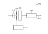
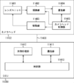
- FIG. 1 It is a figure which shows the use example of the solid-state image sensor of 1st to 9th Embodiment to which this technique is applied. It is a functional block diagram of an example of the electronic device which concerns on the tenth embodiment to which this technique is applied. It is a figure which shows an example of the schematic structure of the endoscopic surgery system. It is a block diagram which shows an example of the functional structure of a camera head and a CCU. It is a block diagram which shows an example of the schematic structure of a vehicle control system. It is explanatory drawing which shows an example of the installation position of the vehicle exterior information detection unit and the image pickup unit.
- Example 7 of solid-state image sensor and Example 7 of image pickup control method 9. Eighth Embodiment (Example 8 of solid-state image sensor and Example 8 of image pickup control method) 10. Ninth Embodiment (Example 9 of solid-state image sensor and example 9 of image pickup control method) 11.
- Example 9 of solid-state image sensor and example 9 of image pickup control method 11.
- Example of electronic device 12.
- Example of using a solid-state image sensor to which this technology is applied 13.
- Example of application to endoscopic surgery system 14.
- a global shutter operation is performed without mounting a frame memory in a pixel configuration having a structure having a holding portion in the pixel (for example, an intra-pixel memory structure, a floating diffusion (FD) storage structure, etc.). Moreover, it is possible to realize two streams (2 streams, signal flow).
- the data can be further rearranged in the image sensor and output in an order in which the image processing LSI (Large Scale Integration) can easily receive the data.
- image processing LSI Large Scale Integration
- this technology gives priority to the pixel data used in the moving image mode in the time-division output still image operation, and can realize a continuous moving image without a break by using it as a moving image.
- other pixel data can be divided and output in the vertical blanking period of the moving image mode, all pixels can be read through several frames, and the still images for all pixels can be completed by combining with the previously read moving image. it can.
- PLS Parastic light sensitivity
- a G (green) filter R (red) filter in the same line. If and G (green) filter are arranged, the G (green) filter is Gr filter, and if B (blue) filter and G (green) filter are arranged in the same row, the G (green) filter is used. Is a Gr filter), it is possible to reduce the in-plane difference of PLS characteristics for each color.
- the PLS difference between colors can be adjusted and absorbed by the white balance gain by calculating the white balance value by, for example, a white balance amplifier provided in the ISP (Image Signal Processor).
- This technology relates to a solid-state image sensor and an electronic device, and an image pickup control method for the solid-state image sensor.
- the solid-state imaging device is a global shutter system, and has a photoelectric conversion unit that generates a charge according to incident light and a holding unit that holds the charge transferred from the photoelectric conversion unit for each pixel.
- a first pixel array unit having a conversion unit that converts the charge into a pixel signal and a plurality of pixels arranged in a matrix is formed, and the pixel signal is read out to generate first pixel data.
- the plurality of pixels included in the solid-state image sensor according to the present technology may be composed of pixels used for image generation, and may include pixels used for image generation and focus detection pixels (phase difference pixels) used for focus adjustment. It may be composed of. Further, the solid-state image sensor according to the present technology may include a frame memory for recording the first pixel data and the second pixel data.
- the electronic device according to the present technology is an electronic device equipped with the solid-state image sensor according to the present technology.
- the imaging control method of the solid-state imaging device is a global shutter method, and a photoelectric conversion unit that generates a charge according to incident light and a holding charge that is transferred from the photoelectric conversion unit are held for each pixel. It is an imaging control method of a solid-state imaging device, which includes a unit and a conversion unit that converts a charge into a pixel signal, and a plurality of pixels are arranged in a matrix to form a pixel array unit.
- the imaging control method includes reading a pixel signal to generate first pixel data, reading a pixel signal to generate second pixel data, and reading the first pixel data and the second pixel data. It is a method that includes outputting independently of each other.
- FIG. 1 is a diagram showing a schematic configuration example of a solid-state image sensor (image sensor) 1000 and an ISP (Image Signal Processor) 2000.
- the solid-state image sensor (image sensor) 1000 includes a GS (global shutter) pixel array unit 1110 and an ADC / signal processing unit 1900
- the ISP 2000 includes an image processing unit 2100.
- N1 shown in FIG. 1 schematically shows stream 1 (stream 1, signal flow 1) between the ADC / signal processing unit 1900 and the image processing unit 2100.
- N2 shown in FIG. 1 schematically shows a stream 2 (stream 2, signal flow 2) between the ADC / signal processing unit 1900 and the image processing unit 2100.
- the GS (global shutter) pixel array unit 1110 shown in FIG. 1 is obtained by photoelectrically converting light incident on a photoelectric conversion element (for example, a photodiode (PD)) (not shown) to obtain a charge. It is converted into a pixel signal (electric signal) at a level corresponding to the charged charge, the pixel signal of each pixel is read out, and A / D conversion (output as a digital signal) is performed by the ADC / signal processing unit 1900.
- pixel data first pixel data, second pixel data, third pixel
- captured image moving image, still image
- Data 4th pixel data, etc.
- the ADC / signal processing unit 1900 outputs the first pixel data (or the third pixel data) as the stream 1 (n1) to the image processing LSI 2100, and the ADC / signal processing unit 1900 outputs the first pixel data (or the third pixel data) to the image processing LSI 2100.
- the second pixel data (or the fourth pixel data) is output to the image processing unit 2100.
- the pixel data may be rearranged in ISP2000 so that appropriate image processing can be performed, if necessary.
- the solid-state image sensor (image sensor) 1000 for example, the first pixel data (or the third pixel data) is set to stream1 (n1), and the second pixel data (or the fourth pixel data) is set to stream2 (n2). , It becomes possible to output to ISP2000 (image processing unit 2100) independently of each other.
- the second pixel data (or the fourth pixel data) is set to stream1 (n1), and the first pixel data (or the third pixel data) is set to stream2 (n2). It is also possible to output to ISP2000 (image processing unit 2100) independently of each other.
- the solid-state image sensor (image sensor) 1000 and the ISP2000 may or may not be provided in the same housing.
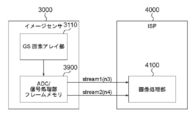
- FIG. 2 is a diagram showing a schematic configuration example of a solid-state image sensor (image sensor) 3000 and an ISP (Image Signal Processor) 4000.
- the solid-state image sensor (image sensor) 3000 includes a GS (global shutter) pixel array unit 3110 and an ADC / signal processing unit / frame memory 3900
- the ISP 4000 includes an image processing unit 4100.
- N3 shown in FIG. 2 schematically shows stream 1 (stream 1, signal flow 1) between the ADC / signal processing unit / frame memory 3900 and the image processing unit 4100.
- N4 shown in FIG. 2 schematically shows stream 2 (stream 2, signal flow 2) between the ADC / signal processing unit / frame memory 3900 and the image processing unit 4100.
- the GS (global shutter) pixel array unit 3110 shown in FIG. 2 is obtained by photoelectrically converting light incident on a photoelectric conversion element (for example, a photodiode (PD)) (not shown) to obtain a charge. It is converted into a pixel signal (electric signal) with a level corresponding to the charged charge, the pixel signal of each pixel is read out, and A / D conversion (output as a digital signal) is performed by the ADC / signal processing unit / frame memory 3900. ), And by performing signal processing, pixel data (first pixel data, second pixel data) for obtaining captured images (moving images, still images) of the subject and data for performing focus adjustment by the phase difference method.
- a photoelectric conversion element for example, a photodiode (PD)
- PD photodiode
- the ADC / signal processing unit / frame memory 3900 outputs the first pixel data (or the third pixel data) as the stream 1 (n3) to the image processing unit 4100, and the ADC / signal processing unit / frame memory. From 3900, the second pixel data (or the fourth pixel data) is output to the image processing LSI unit 4100 as stream2 (n4).
- the first pixel data (or the third pixel data) is set to stream1 (n3)
- the second pixel data (or the fourth pixel data) is set to stream2 (n4).
- ISP4000 image processing unit 4100
- the second pixel data (or the fourth pixel data) is set to stream1 (n3)
- the first pixel data (or the third pixel data) is set to stream2 (n4). It is also possible to output to the ISP 4000 (image processing unit 4100) independently of each other.
- the solid-state image sensor (image sensor) 3000 and the ISP 4000 may or may not be provided in the same housing.
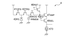
- FIG. 3 is an equivalent circuit diagram showing a configuration example of pixels for a global shutter included in a solid-state image sensor to which the present technology is applied.
- the pixel (MEM holding type) 4 shown in FIG. 3 shows a configuration for realizing an electronic global shutter function.
- the pixel 4 includes a photodiode (PD) 42 as a photoelectric conversion element, a transfer gate (TRG: Transistor Gate) 43, a holding unit (MEM: in-pixel memory) 44, and a read-out gate (ROG: Read Out Gate). 45, FD (floating diffusion region) 49, reset gate (RST: Reset Gate) 46, amplification transistor (AMP: AMPTr) 47, selection transistor (SEL: SELTr) 48, overflow gate (OFG: OverFlow). Gate) 41 and.
- PD photodiode
- TRG Transistor Gate
- MEM in-pixel memory
- ROG Read Out Gate
- the photodiode (PD) 42 is a photoelectric conversion unit that generates and stores an electric charge (signal charge) according to the amount of received light.
- the anode terminal of the photodiode (PD) 42 is grounded, and the cathode terminal is connected to the holding unit (MEM: intrapixel memory) 44 via the transfer gate (TRG: Transfer Gate) 43. Further, the cathode terminal of the photodiode (PD) 42 is also connected to an overflow gate (OFG: OverFlow Gate) 41 for discharging unnecessary charges.
- OFG OverFlow Gate
- TRG Transfer Gate
- PD photodiode
- MEM in-pixel memory
- the FD 49 is a conversion unit and a holding unit that converts the electric charge read from the holding unit (MEM: in-pixel memory) 44 as a signal and holds it for reading.
- the reset gate (RST: Reset Gate) 46 When the reset gate (RST: Reset Gate) 46 is turned on, the electric charge stored (retained) in the FD 49 is discharged to the constant voltage source VDD, so that the potential of the FD 49 can be reset.
- the amplification transistor (AMP: AMPTr) 47 outputs a pixel signal corresponding to the potential of the FD49. That is, the amplification transistor (AMP: AMPTr) 47 constitutes a load MOS 470 as a constant current source and a source follower circuit, and a pixel signal indicating a level corresponding to the electric charge stored (held) in the FD 49 is an amplification transistor (AMP). : AMPTr) 47 is output to, for example, a column signal processing circuit (not shown) via a selection transistor (SEL: SELTr) 48.
- the load MOS 470 is arranged in, for example, a column signal processing circuit.
- the selection transistor (SEL: SELTr) 48 When the pixel 4 is selected and turned on, the selection transistor (SEL: SELTr) 48 outputs the pixel signal of the pixel 4 to, for example, a column signal processing circuit (not shown) via a vertical signal line (not shown). To do.
- the overflow gate (OFG: OverFlow Gate) 41 is turned on, the electric charge accumulated in the photodiode (PD) 42 is discharged to the constant voltage source VDD, and the photodiode (PD) of all pixels is discharged. ) 42 is reset (sometimes referred to as a global reset (GR)).
- OFG OverFlow Gate
- the overflow gate (OFG: OverFlow Gate) 41 is turned off, and exposure is started for all pixels in the pixel array section.
- TRG Transfer Gate
- PD photodiode
- the transfer gate (TRG: Transfer Gate) 43 is turned off, the electric charge held in the holding unit (MEM: intra-pixel memory) 44 of each pixel 4 is sequentially, for example, a column signal in row units of the pixel array unit.
- the read-out gate (ROG: Read Out Gate) 45 of the pixel 4 in the read line is turned on, and the electric charge held in the holding unit (MEM: intra-pixel memory) 44 is transferred to the FD 49.
- the selection transistor (SEL: SELTr) 48 is turned on, a signal (pixel signal) indicating the level corresponding to the electric charge stored in the FD 49 is transmitted from the amplification transistor (AMP: AMPTr) 47 to the selection transistor (SEL). : SELTr) 48 is read out and output to the column signal processing circuit.
- the exposure time is set to be the same for all the pixels of the pixel array unit, and after the exposure is completed, the electric charge is temporarily charged to the holding unit (MEM: in-pixel memory) 44.
- MEM in-pixel memory
- a global shutter method in which electric charges are sequentially read from the holding unit (MEM: in-pixel memory) 44 in line units, the electric charges are converted into pixel signals by the FD 49, and the pixel signals are read out and output. Operation (imaging) is possible.
- FIG. 4 is an equivalent circuit diagram showing a configuration example of pixels for a global shutter included in a solid-state image sensor to which the present technology is applied.
- the pixel (FD holding type) 5 shown in FIG. 4 shows a configuration for realizing an electronic global shutter function.
- Pixels 5 include a photodiode (PD) 52 as a photoelectric conversion element, a transfer gate (TRG: Transfer Gate) 53, an FD (floating diffusion region) 59, a reset gate (RST: Reset Gate) 56, and an amplification transistor. It has (AMP: AMPTr) 57, a selection transistor (SEL: SELTr) 58, and an overflow gate (OFG: OverFlow Gate) 51.
- PD photodiode
- TRG Transfer Gate
- FD floating diffusion region
- RST Reset Gate
- AMP AMPTr
- SEL selection transistor
- OFG OverFlow Gate
- the photodiode (PD) 52 is a photoelectric conversion unit that generates and stores an electric charge (signal charge) according to the amount of received light.
- the anode terminal of the photodiode (PD) 52 is grounded, and the cathode terminal is connected to the FD (floating diffusion region) 59 via a transfer gate (TRG: Transfer Gate) 53. Further, the cathode terminal of the photodiode (PD) 52 is connected to an overflow gate (OFG: OverFlow Gate) 51 for discharging unnecessary charges.
- OFG OverFlow Gate
- TRG Transfer Gate
- the FD 59 is a conversion unit and a holding unit that converts the read charge as a signal and holds it for reading.
- the reset gate (RST: Reset Gate) 56 is turned on, the electric charge stored (retained) in the FD 59 is discharged to the constant voltage source VDD, so that the potential of the FD 59 can be reset.
- the amplification transistor (AMP: AMPTr) 57 outputs a pixel signal corresponding to the potential of the FD 59. That is, the amplification transistor (AMP: AMPTr) 57 constitutes a load MOS 570 as a constant current source and a source follower circuit, and a pixel signal indicating a level corresponding to the electric charge stored (held) in the FD 59 is an amplification transistor (AMP). : AMPTr) 57 is output to, for example, a column signal processing circuit (not shown) via a selection transistor (SEL: SELTr) 58.
- the load MOS 570 is arranged in, for example, a column signal processing circuit.
- the selection transistor (SEL: SELTr) 58 When the pixel 5 is selected and turned on, the selection transistor (SEL: SELTr) 58 outputs the pixel signal of the pixel 5 to, for example, a column signal processing circuit (not shown) via a vertical signal line (not shown). To do.
- the overflow gate (OFG: OverFlow Gate) 51 When the overflow gate (OFG: OverFlow Gate) 51 is turned on, the unnecessary charge stored in the photodiode (PD) 52 is discharged to the constant voltage source VDD.
- OFG OverFlow Gate
- the overflow gate (OFG: OverFlow Gate) 51 is turned on, the electric charge accumulated in the photodiode (PD) 52 is discharged to the constant voltage source VDD, and the photodiode (PD) of all pixels is discharged. ) 52 is reset (sometimes referred to as a global reset (GR)).
- OFG OverFlow Gate
- the overflow gate (OFG: OverFlow Gate) 51 is turned off, and exposure is started for all pixels in the pixel array section.
- TRG Transfer Gate
- PD photodiode
- the selection transistor (SEL: SELTr) 58 is turned on, so that a signal (pixel signal) indicating a level corresponding to the electric charge accumulated (retained) in the FD 59 is turned on. ) Is read from the amplification transistor (AMP: AMPTr) 57 to the column signal processing circuit via the selection transistor (SEL: SELTr) 58 and output.
- AMP amplification transistor
- SEL SELTr
- the exposure time is set to be the same for all the pixels of the pixel array unit, and after the exposure is completed, the charge is held and accumulated in the FD 59, and the charge is further stored in the pixels. It is possible to perform a global shutter operation (imaging) that converts a signal into a signal and sequentially reads and outputs a pixel signal from the FD 59 line by line.
- imaging converts a signal into a signal and sequentially reads and outputs a pixel signal from the FD 59 line by line.
- FIG. 5 is a diagram showing a configuration example of a filter pattern that can be used in a solid-state image pickup device to which the present technology is applied.
- FIG. 5A shows a Bayer array structure 6a of a color filter.
- FIG. 5B shows a pattern structure 6b of a black and white filter (without a color filter).
- the Bayer array structure 6a of the color filter shown in FIG. 5A includes the red filter 6aR, the green filter 6aGr arranged on the right side of the red filter 6aR (the right side in FIG. 5A), and the red color.
- the green filter 6aGb arranged on the lower side of the filter 6aR (lower side in FIG. 5A) and the blue filter 6aB arranged on the right side of the green filter 6aGb (right side in FIG. 5A) are combined. As a set, the set is repeatedly formed.
- one photodiode is formed corresponding to each of the red filter 6aR, the green filter 6aGr, the green filter 6aGb, and the blue filter 6aB, and the red filter 6aR, the green filter 6aGr, the green filter 6aGb, and the blue filter 6aB are formed.
- Each of these can be considered as one pixel (unit pixel).
- the pattern structure 6b of the black-and-white filter (without color filter) shown in FIG. 5B includes a black filter 6bBL1 and a white filter 6bW1 arranged on the right side of the black filter 6bBL1 (the right side in FIG. 5B).
- the set is repeatedly formed.
- one photodiode is formed corresponding to each of the black filter 6bBL1, the white filter 6bW1, the white filter 6bW2, and the black filter 6bBL2, and the black filter 6bBL1, the white filter 6bW1, the white filter 6bW2, and the black filter 6bBL2 are formed.
- Each of these can be considered as one pixel (unit pixel).
- the pattern structure 6b of the black-and-white filter (without the color filter) shown in FIG. 5B may include, for example, a gray filter in which the gray density is gradually changed, or the gray density may be gradually changed. It may be composed of a gray filter changed to.
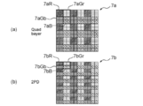
- FIG. 6 is a diagram showing a configuration example of a filter pattern that can be used in a solid-state image sensor to which the present technology is applied. Specifically, FIG. 6A shows a quad Bayer array structure 7a of a color filter. FIG. 6B shows a 2PD (photodiode) array structure 7b of a color filter.
- FIG. 6A shows a quad Bayer array structure 7a of a color filter.
- FIG. 6B shows a 2PD (photodiode) array structure 7b of a color filter.
- the quadbayer arrangement structure 7a of the color filter shown in FIG. 6A is a group of red filters composed of four red filters (two red filters on the left and right and two red filters on the top and bottom in FIG. 6A).
- a set of blue filter groups 7aB composed of a blue filter) is formed as a set, and the set is repeated.
- a diode (PD) is formed, and one on-chip lens is formed corresponding to each of the red filter group 7aR, the green filter group 7aGr, the green filter group 7aGb, and the blue filter group 7aB, and four filters (four) are formed.
- Each of the red filter group 7aR, the green filter group 7aGr, the green filter group 7aGb, and the blue filter group 7aB composed of the photodiode (PD)) can be considered as one pixel (unit pixel).
- the 2PD (photonode) array structure 7b of the color filter shown in FIG. 6 (b) includes a red filter group 7bR composed of two red filters (two red filters on the left and right in FIG. 6 (b)) and a red filter group.
- a green filter group 7bGr consisting of two green filters (two green filters on the left and right in FIG. 6B) arranged on the right side of the 7bR (the right side in FIG. 6B) and a lower side of the red filter group 7bR.
- a green filter group 7bGb consisting of two green filters (two green filters on the left and right in FIG. 6B) arranged (lower side in FIG. 6B) and a right side of the green filter group 7bGb (FIG. 6).
- a blue filter group 7bB consisting of two blue filters (two left and right blue filters in FIG. 6B) arranged on the right side in (b) is set as a set, and the set is repeatedly formed. Has been done.
- a diode (PD) is formed to form one on-chip lens corresponding to each of the red filter group 7bR, the green filter group 7bGr, the green filter group 7bGb, and the blue filter group 7bB, and two filters (two).
- Each of the red filter group 7bR, the green filter group 7bGr, the green filter group 7bGb, and the blue filter group 7bB composed of the photodiode (PD)) can be considered as one pixel (unit pixel).
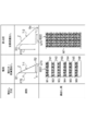
- FIG. 7 is a diagram showing a reading method for moving images and still images, a figure schematically showing the reading method (reading figure), and a reading example using a pixel array unit of 10 columns ⁇ 24 rows as an example.
- FIG. 8 is a diagram showing a reading method for a divided still image, a figure (reading figure) schematically showing the reading method, and a reading example using a pixel array unit of 10 columns ⁇ 24 rows as an example.
- the moving image reading method is thinning / addition reading
- the still image reading method is all pixel reading
- the divided still image reading method is all pixels. It is a time-division reading of.
- the horizontal axis X of each of the figures 7-1 to 7-6 (right triangle) of the moving image reading method, the still image reading method, and the divided still image reading method represents the time axis, and the arrow Q70 represents the passage of time. ..
- the vertical axis Y represents the physical position of the pixel array unit (screen), and the arrow P70 indicates that the reading is performed from the ascending line to the descending line.
- Z roughly represents the read position and read time of the pixel (pixel signal).
- the apex R1 (the uppermost part of the vertical axis Y and the leftmost part of the horizontal axis X) of the read figure 7-1 for obtaining the image data of the moving image (image data of the first frame) is the most of the pixel array part (screen). It is the upper read line (the read line on the upper side of M1 for two read lines of the pixel array unit (screen) 6001 in the read example), and represents the time for starting reading.
- the vertex R2 of the figure 7-1 (the lowest part of the vertical axis Y and the rightmost part of the horizontal axis X) is the reading line at the bottom of the pixel array part (screen) (reading of the pixel array part (screen) 6001 in the reading example). It is the lower line of M6 for two lines) and represents the time for completing reading. That is, the reading direction in the reading figure 7-1 is read from the upper line to the lower line in line units.
- the apex R3 (the uppermost part of the vertical axis Y and the leftmost part of the horizontal axis X) of the read figure 7-2 for obtaining the image data of the still image is the readout line (reading example) of the uppermost part of the pixel array part (screen). It is the reading line of the uppermost part of M7 for 24 reading lines of the pixel array part (screen) 6002 in the above, and represents the time of reading start.
- the apex R4 of the figure 7-2 (the lowest part of the vertical axis Y and the rightmost part of the horizontal axis X) is the reading line of the lowermost part of the pixel array part (screen) (reading of the pixel array part (screen) 6002 in the reading example). It is the reading line at the bottom of 24 lines) and represents the reading end time. That is, the reading direction in the reading figure 7-2 is read from the upper line to the lower line in line units.
- the apex R5 (the uppermost part of the vertical axis Y and the leftmost part of the horizontal axis X) of the reading figure 7-3 for obtaining the image data of the divided still image 1 is the reading line (the uppermost part of the pixel array part (screen)). It is the reading line on the upper side of M8 for two reading lines of the pixel array unit (screen) 6003 in the reading example), and represents the time for starting reading.
- the apex R2 of the figure 7-3 (the lowest part of the vertical axis Y and the rightmost part of the horizontal axis X) is the reading line at the bottom of the pixel array part (screen) (reading of the pixel array part (screen) 6003 in the reading example). It is the lower line of M13 for two lines) and represents the time for completing reading. That is, the reading direction in the reading figure 7-3 is read from the upper line to the lower line in line units.
- the apex R7 (the uppermost part of the vertical axis Y and the leftmost part of the horizontal axis X) of the reading figure 7-4 for obtaining the image data of the divided still image 2 is the reading line (the uppermost part of the pixel array part (screen)). It is the reading line on the upper side of M14 for two reading lines of the pixel array unit (screen) 6004 in the reading example), and represents the time for starting reading.
- the apex R8 of the figure 7-4 (the lowest part of the vertical axis Y and the rightmost part of the horizontal axis X) is the reading line at the bottom of the pixel array part (screen) (reading of the pixel array part (screen) 6004 in the reading example). It is the lower line of M15 for two lines) and represents the time for completing reading. That is, the reading direction in the reading figure 7-4 is read from the upper line to the lower line in line units.
- the apex R9 (the uppermost part of the vertical axis Y and the leftmost part of the horizontal axis X) of the read figure 7-5 for obtaining the image data of the divided still image 3 is the readout line (the uppermost part of the pixel array part (screen)). It is the reading line on the upper side of M16 for two reading lines of the pixel array unit (screen) 6005 in the reading example), and represents the time for starting reading.
- the apex R10 of the figure 7-5 (the lowest part of the vertical axis Y and the rightmost part of the horizontal axis X) is the reading line at the bottom of the pixel array part (screen) (reading of the pixel array part (screen) 6005 in the reading example). It is the lower line of M17 for two lines) and represents the time for completing reading. That is, the reading direction in the reading figure 7-5 is read from the upper line to the lower line in line units.
- the apex R10 (top of the vertical axis Y, leftmost of the horizontal axis X) of the read figure 7-6 for obtaining the image of the divided still image 4 is the read line (read) at the top of the pixel array part (screen). It is the reading line on the upper side of M19 for two reading lines of the pixel array unit (screen) 6006 in the example), and represents the time for starting reading.
- the apex R10 of the figure 7-6 (the lowest part of the vertical axis Y and the rightmost part of the horizontal axis X) is the reading line at the bottom of the pixel array part (screen) (reading of the pixel array part (screen) 6006 in the reading example). It is the lower line of M19 for two lines) and represents the time for completing reading. That is, the reading direction of the reading figure 7-6 is read from the upper line to the lower line in line units.
- the reading method for obtaining a moving image is thinning / addition reading.
- the moving image reading method reads out two rows of M1 pixels (pixel signals) in line units in order from the upper side of the pixel array unit (screen) 6001, and two rows of M2 pixels.
- Pixel signal is read, M3 pixels (pixel signal) for two lines are read, M4 pixels (pixel signal) for two lines are read, and M5 pixels (pixels) for two lines are read.
- the signal) is read, the pixels (pixel signals) of M6 for two lines are read, the readings of M1 to M6 are added (a total of 12 lines are added in FIG. 7), and further, the pixel array unit (pixel array unit).
- N1 pixels are thinned out (without reading), and two rows of N2 pixels (pixel signals) are thinned out (without reading).
- Two rows of N3 pixels (pixel signals) are thinned out (without reading), two rows of N4 pixels (pixel signals) are thinned out (without reading), and two rows of N5 pixels (pixels)
- the signal) is thinned out (without reading), the pixels (pixel signals) of N6 for two lines are thinned out (without reading out), and in FIG. 7, a total of 12 lines are thinned out to make a moving image (moving image).
- the image of the frame (the image of the first frame) is obtained.
- the reading method for obtaining a moving image is thinned out, and the reading time is shortened.
- the reading time for obtaining a moving image is half of the reading time for obtaining a still image.
- the length in the X-axis direction of the readout figure 7-1 for obtaining the image data of the moving image (image data of the first frame) is the length in the X-axis direction of the readout figure 7-2 for obtaining the image data of the still image. It is about half the length of the image.
- the readout method for obtaining a still image is all-pixel readout. Specifically, in the still image reading method, M7 pixels (pixel signals) for all pixels are read in order from the upper side of the pixel array unit (screen) 6002 in line units to obtain a still image (still image). Is obtained.
- the reading method for obtaining the image of the divided still image is time-division reading of all pixels.
- two rows of M8 pixels (pixel signals) are read in row units in order from the upper side of the pixel array unit (screen) 6003 for two rows.
- M9 pixel (pixel signal) is read, two rows of M10 pixels (pixel signal) are read, two rows of M11 pixels (pixel signal) are read, and two rows of M12 are read.
- Pixel (pixel signal) is read, two rows of M13 pixels (pixel signal) are read, M8 to M13 are added (in FIG. 7, a total of 12 rows are added), and further.
- N7 pixels Two rows of N7 pixels (pixel signals) are thinned out (without reading) and two rows of N8 pixels (pixel signals) are thinned out (read) in order from the upper side of the pixel array unit (screen) 6003.
- Two lines of N9 pixels are thinned out (without reading) and two lines of N10 pixels (pixel signals) are thinned out (without reading) for two lines.
- N12 pixels pixel signals
- two lines of N13 pixels are thinned out (without reading) are thinned out (without reading)
- a total of 12 lines are thinned out.
- a divided still image 1 (divided still image 1) is obtained.
- the divided still images 1 to 4 are added together to obtain a still image (still image), and the divided still image 1 (divided still image 1) is a frame of a moving image (moving image). Can be used as the image of (the image of the second frame).
- the pixel array unit 6003 to the pixel array unit 6006 are distinguished as reference numerals, but the pixel array units of the pixel array unit 6003 to the pixel array unit 6006 are the same pixel array unit (same screen). ).
- the contents described with reference to FIGS. 7 and 8 are described in the first embodiment (example 1 of the solid-state image sensor and the example 1 of the image pickup control method) and the second embodiment (example 2 of the solid-state image sensor) described later. 2), a third embodiment (Example 3 of a solid-state image sensor and an example 3 of an image pickup control method), and a fourth embodiment (Example 4 of a solid-state image sensor and Example 4 of an image pickup control method).
- 5th embodiment Example 5 of solid-state image sensor and Example 5 of image pickup control method
- 6th embodiment Example 6 of solid-state image sensor and Example 6 of image pickup control method
- FIG. 17 is a perspective view showing a configuration example of a solid-state image sensor to which the present technology is applied.
- FIG. 17A is a support substrate laminated type solid-state image sensor 14a
- FIG. 17B is a support substrate laminated type solid-state image sensor.
- FIG. 17 (c) is a circuit stacking (3 layers) type solid-state image sensor 14c
- FIG. 17 (d) is a circuit stacking (3 layers).
- Type solid-state image sensor 14d is a perspective view showing a configuration example of a solid-state image sensor to which the present technology is applied.
- FIG. 17A is a support substrate laminated type solid-state image sensor 14a
- FIG. 17B is a support substrate laminated type solid-state image sensor.
- FIG. 17 (c) is a circuit stacking (3 layers) type solid-state image sensor 14c
- FIG. 17 (d) is
- the solid-state image sensor 14a shown in FIG. 17A is configured by bonding the substrate 146a and the support substrate 142a in the directions of arrow P14 and arrow Q14.
- a pixel (pixel array unit, pixel area) 140a and a circuit (function mounting unit) 141a are formed on the substrate 146a.
- a logic unit 144a, an accessory unit 145a, a column unit 143a, and a logic unit 144a are formed in the circuit (function mounting unit) 141a in this order from the left side in FIG. 17A. That is, an accessory unit 145a and a column unit 143a are arranged between the two logic units 144a.
- the solid-state image sensor 14b shown in FIG. 17B is configured by bonding the sensor substrate 147b and the circuit board 148b in the directions of arrow P14 and arrow Q14.
- pixels (pixel array unit, pixel area) 140b are formed on the sensor substrate 147b
- a circuit (function mounting portion) 141b is formed on the circuit board 148b.
- the circuit (function mounting portion) 141b is formed with an accessory portion 145b, a column portion 143b, and a logic portion 144b on the accessory portion 145b and the column portion 143b. That is, the logic portion 144b is laminated and arranged on the accessory portion 145b and the column portion 143b arranged in the same layer (same height).
- the sensor substrate 147c In the solid-state image sensor 14c shown in FIG. 17 (c), the sensor substrate 147c, the frame memory (DRAM (Dynamic Random Access Memory) 146c, and the circuit board 148c are arranged in this order in the arrow P14 direction and the arrow Q14 direction (in this order).
- the sensor substrate 147c is formed with pixels (pixel array unit, pixel area) 140c, as shown in FIG. 17 (c), which are formed by laminating the arrow P14 and the arrow Q14 in opposite directions.
- a circuit (function mounting unit) 141c is formed on the circuit board 148c.
- the circuit (function mounting unit) 141c has an accessory unit 145c, a column unit 143c, an accessory unit 145c, and a logic unit 144c on the column unit 143c. That is, the logic portion 144c is laminated and arranged on the accessory portion 145c and the column portion 143c arranged in the same layer (same height).
- a sensor substrate 147d, a circuit board 148d, and a frame memory (DRAM (Dynamic Random Access Memory) 146d are arranged in this order in the directions of arrow P14 and arrow Q14.
- pixels (pixel array unit, pixel area) 140d are formed on the sensor substrate 147d, and a circuit (function mounting portion) is formed on the circuit board 148d.
- 141d is formed.
- an accessory portion 145d, a column portion 143d, and a logic portion 144d on the accessory portion 145d and the column portion 143d are formed, that is, the same layer.
- the logic portion 144d is laminated and arranged on the accessory portion 145d and the column portion 143d arranged at (the same height).
- any one of the solid-state image pickup devices 14a to 14d shown in FIGS. 17 (a) to 17 (d) can be applied to the present technology.
- FIG. 9 (a) in FIG. 9 shows a two-stream (2 stream) drive operation in a global shutter system that can be realized by Example 1 (without frame memory) of the solid-state image sensor according to the first embodiment according to the present technology. It is a figure which shows the example (example 1 of the image pickup control method) 5001a.
- the first pixel data is output as Stream1
- the second pixel data is Stream2, which is separate from Stream1.
- the pixel data 8-1 of the moving image (moving image frame) to the pixel data 8-7 of the moving image (moving image frame) constituting the first pixel data are output as Stream 1 in the order of time series, and the first The pixel data 9-3 of the split still image 1, the pixel data 9-34 of the split still image 2, the pixel data 9-45 of the split still image 3, and the split still image constituting the two-pixel data in chronological order.
- the pixel data 9-56 of the image 4 is output separately and independently as Stream 2. Then, it is obtained from each of the pixel data 9-3 of the divided still image 1, the pixel data 9-34 of the divided still image 2, the pixel data 9-45 of the divided still image 3, and the pixel data 9-56 of the divided still image 4.
- the still images (still images) for all the pixels of the pixel array unit (screen) are obtained. Be done. Further, since the pixel data 9-3 of the divided still image 1 and the pixel data 8-3 of the moving image can be shared by the time-divided output still image operation, the moving image (moving image) can have continuous continuity. A still image (still image) can be smoothly produced.
- Reference numeral 5001 indicates the flow of reading from the pixels of the pixel array unit (screen) in time series.
- T81 to T87 in which the numerical order of the reference numerals means a time series, roughly indicates the time from the start of pixel reading to the memory transfer (MEM Transfer) in frame rate.
- MEM Transfer memory transfer
- each of T81 to T87 is 120 fps (8.3 ms).
- the reading flow 5001 will be explained in more detail.
- the T81 sets the read start time indicated by the apex R13 of the figure 30-1, which schematically displays the read for obtaining the image data (image data of the first frame) of the moving image by the output of the pixel data 8-1 of the moving image.
- the charge accumulated in the photodiode (PD) of each pixel for reading in the next T82 is transferred to the holding unit (MEM: intra-pixel memory) all at once (memory transfer (MEM). Transfer) 82) Time is the end.
- the photodiodes (PD) of all the pixels are reset all at once before the end of reading indicated by the apex R14 of the figure 30-1 (global reset (GR) 81). ..
- the T82 sets the read start time indicated by the apex R15 of the figure 30-2 schematically displaying the read for obtaining the image data (image data of the first frame) of the moving image by the output of the pixel data 8-2 of the moving image.
- the charge accumulated in the photodiode (PD) of each pixel for reading in the next T83 is transferred to the holding unit (MEM: intra-pixel memory) all at once (memory transfer (MEM). Transfer) 82) Time is the end.
- the photodiodes (PD) of all the pixels are reset all at once before the end of reading indicated by the apex R16 of the figure 30-2 (global reset (GR) 81). ..
- the T83 is an image data of the moving image (image data of the second frame) obtained by outputting the pixel data 8-3 of the moving image and an image data of the divided still image (image data of the divided still image 1) obtained by outputting the pixel data 9-3 of the divided still image.
- the photodiode (PD) of each pixel for the next T84 read, starting from the read start time indicated by the vertex R17 of the figure 300-3 which schematically displays the read for obtaining both of the image data).
- the end time is (memory transfer (MEM Transfer) 82) in which all the pixels are collectively transferred to the holding unit (MEM: intra-pixel memory).
- MEM Transfer memory transfer
- the photodiodes (PD) of all the pixels are reset all at once before the end of reading indicated by the apex R18 of the figure 300-3 (global reset (GR) 81). ..
- the moving image pixel data 8-3 obtained by reading the pixels (pixel signals) based on the figure 300-3 is, for example, an image processing unit in order to obtain the moving image image data (image data of the second frame) as the first pixel data.
- the pixel data 9-3 of the divided still image is output to (ISP) as Stream 1 in order to obtain the image data of the divided still image (image data of the divided still image 1) as the second pixel data. It is output to ISP) as Stream 2 separately and independently.
- the figure 300-34 schematically displaying the reading for obtaining the image data of the divided still image (the image data of the divided still image 2) output from 9-34 is shown, and the apex R19 of the figure 300-34 is read. The start is indicated, and the peak R20 in FIGS. 300-34 indicates the end of reading.
- the T84 sets the read start time indicated by the apex R21 of the figure 30-4 schematically displaying the read for obtaining the image data (image data of the first frame) of the moving image by the output of the pixel data 8-4 of the moving image.
- the charge accumulated in the photodiode (PD) of each pixel for reading in the next T85 is transferred to the holding unit (MEM: intra-pixel memory) all at once (memory transfer (MEM). Transfer) 82) Time is the end.
- the photodiodes (PD) of all pixels are reset all at once before the end of reading indicated by the apex R22 of the figure 30-4 (global reset (GR) 81). ..
- Figure 300-45 is shown which schematically displays the reading for obtaining the image data of the divided still image (image data of the divided still image 3) by the output of 9-45, and the apex R23 of the figure 300-45 is read. The start is indicated, and the apex R24 of the figure 300-45 indicates the end of reading.
- the T85 sets the read start time indicated by the apex R25 of the figure 30-5 schematically displaying the read for obtaining the image data (image data of the first frame) of the moving image by the output of the pixel data 8-5 of the moving image.
- the charge accumulated in the photodiode (PD) of each pixel for reading in the next T86 is transferred to the holding unit (MEM: intra-pixel memory) all at once (memory transfer (MEM). Transfer) 82) Time is the end.
- the photodiodes (PD) of all the pixels are reset all at once before the end of reading indicated by the apex R26 of the figure 30-5 (global reset (GR) 81).
- the pixel data of the divided still image is shown, and the apex R27 of the figure 300-56 is read. The start is indicated, and the apex R28 of the figure 300-56 indicates the end of reading.
- the T86 sets the read start time indicated by the apex R29 of the figure 30-6 schematically displaying the read for obtaining the image data (image data of the first frame) of the moving image by the output of the pixel data 8-6 of the moving image.
- the charge accumulated in the photodiode (PD) of each pixel for reading in the next T87 is transferred to the holding unit (MEM: intra-pixel memory) all at once (memory transfer (MEM). Transfer) 82) Time is the end.
- the photodiodes (PD) of all the pixels are reset all at once before the end of reading indicated by the apex R30 of the figure 30-6 (global reset (GR) 81).
- the T87 sets the read start time indicated by the apex R31 of the figure 30-7 schematically displaying the read for obtaining the image data (image data of the first frame) of the moving image by the output of the pixel data 8-7 of the moving image.
- the charge accumulated in the photodiode (PD) of each pixel for reading in the next T88 is transferred to the holding unit (MEM: in-pixel memory) all at once.
- MEM memory transfer
- time is set as the final stage.
- the photodiodes (PD) of all the pixels are reset all at once before the end of reading indicated by the apex R32 of the figure 30-7 (global reset (GR) 81).
- the solid-state image pickup device and the image pickup control method of the first embodiment (Example 1 of the solid-state image sensor and Example 1 of the image pickup control method) according to the present technology are particularly technically inconsistent in addition to the contents described above.
- the contents described in the columns of the solid-state image sensor and the image pickup control method of the second to ninth embodiments according to the present technology described later can be applied as they are.
- Example 2 of solid-state image sensor and Example 2 of image pickup control method The solid-state image pickup device and the image pickup control method of the second embodiment (Example 2 of the solid-state image pickup device and Example 2 of the image pickup control method) according to the present technology will be described with reference to FIG. FIG. 9B in FIG. 9 shows a two-stream (2stream) drive operation in a global shutter system that can be realized by Example 2 (with a frame memory) of the solid-state image sensor of the second embodiment according to the present technology. It is a figure which shows the example (example 2 of the image pickup control method) 5001b.
- the first pixel data is output as Stream 1
- the second pixel data is recorded in the frame memory.
- the second pixel data is rearranged, and the rearranged second pixel data is output as Stream 2 separately from Stream 1.
- the pixel data 10-1 of the moving image (moving image frame) to the pixel data 10-7 of the moving image (moving image frame) constituting the first pixel data are output as Stream 1 in the order of time series, and the first The pixel data 11-3 of the divided still image 1, the pixel data 11-34 of the divided still image 2, the pixel data 11-45 of the divided still image 3, and the divided still image constituting the two-pixel data in chronological order.
- the pixel data 11-56 of the image 4 is output separately and independently as Stream 2.
- Reference numeral 5001 indicates a flow of reading from pixels (pixel signals) of the pixel array unit (screen) in time series.
- T81 to T87 in which the numerical order of the reference numerals means a time series, roughly indicates the time from the start of pixel reading to the memory transfer (MEM Transfer) in frame rate.
- MEM Transfer memory transfer
- each of T81 to T87 is 120 fps (8.3 ms).
- the reading flow 5001 will be explained in more detail.
- the T81 sets the read start time indicated by the apex R13 of the figure 30-1, which schematically displays the read for obtaining the image data (image data of the first frame) of the moving image by the output of the pixel data 10-1 of the moving image.
- the charge accumulated in the photodiode (PD) of each pixel for reading in the next T82 is transferred to the holding unit (MEM: intra-pixel memory) all at once (memory transfer (MEM). Transfer) 82) Time is the end.
- the photodiodes (PD) of all the pixels are reset all at once before the end of reading indicated by the apex R14 of the figure 30-1 (global reset (GR) 81). ..
- the T82 sets the read start time indicated by the apex R15 of the figure 30-2 schematically displaying the read for obtaining the image data (image data of the first frame) of the moving image by the output of the pixel data 10-2 of the moving image.
- the charge accumulated in the photodiode (PD) of each pixel for reading in the next T83 is transferred to the holding unit (MEM: intra-pixel memory) all at once (memory transfer (MEM). Transfer) 82) Time is the end.
- the photodiodes (PD) of all the pixels are reset all at once before the end of reading indicated by the apex R16 of the figure 30-2 (global reset (GR) 81). ..
- the T83 is an image data of the moving image (image data of the second frame) obtained by outputting the pixel data 10-3 of the moving image and an image data of the divided still image (image data of the divided still image 1) obtained by outputting the pixel data 11-3 of the divided still image.
- the photodiode (PD) of each pixel for the next T84 read, starting from the read start time indicated by the vertex R17 of the figure 300-3 which schematically displays the read for obtaining both of the image data).
- the end time is (memory transfer (MEM Transfer) 82) in which all the pixels are collectively transferred to the holding unit (MEM: intra-pixel memory).
- MEM Transfer memory transfer
- the photodiodes (PD) of all the pixels are reset all at once before the end of reading indicated by the apex R18 of the figure 300-3 (global reset (GR) 81). ..
- the moving image pixel data 10-3 obtained by reading the pixels (pixel signals) based on the figure 300-3 is, for example, an image processing unit in order to obtain moving image image data (image data of the second frame) as the first pixel data. It is output as Stream 1 to (ISP), and the pixel data 11-3 of the divided still image is once the arrow P1 in order to obtain the image data of the divided still image (image data of the divided still image 1) as the second pixel data. According to the direction, the memory output Q1 is output to the frame memory and recorded.
- the pixel data 11-34 of the divided still image, the pixel data 11-45 of the divided still image, the pixel data 11-56 of the divided still image, and the pixel data 11-3 of the divided still image are recorded. Is properly rearranged in the frame memory so that still images for all pixels can be appropriately obtained, and then output to the image processing unit (ISP) as Stream 2 independently and independently.
- ISP image processing unit
- Figures 300-34 are shown which schematically display the reading for obtaining the image data of the divided still image (image data of the divided still image 2) by the output of 11-34, and the apex R19 of the figure 300-34 is the reading. It shows the start and the end of the reading with the peak R20 in FIGS. 300-34.
- the pixel data 11-34 of the divided still image is also recorded once with the memory output Q1 in the frame memory according to the direction of the arrow P1 in the same manner as the pixel data 11-3 of the divided still image, and then recorded. It is output separately and independently as Stream 2 to the image processing unit (ISP).
- ISP image processing unit
- the T84 sets the read start time indicated by the apex R21 of the figure 30-4 schematically displaying the read for obtaining the image data (image data of the first frame) of the moving image by the output of the pixel data 10-4 of the moving image.
- the charge accumulated in the photodiode (PD) of each pixel for reading in the next T85 is transferred to the holding unit (MEM: intra-pixel memory) all at once (memory transfer (MEM). Transfer) 82) Time is the end.
- the photodiodes (PD) of all pixels are reset all at once before the end of reading indicated by the apex R22 of the figure 30-4 (global reset (GR) 81). ..
- FIG. 300-45 schematically displaying the reading for obtaining the image data of the divided still image (data of the divided still image 3) output from 11-45 is shown, and the apex R23 of the figure 300-45 starts reading. , And the apex R24 of the figure 300-45 indicates the end of reading.
- the pixel data 11-45 of the divided still image is also recorded once with the memory output Q1 in the frame memory according to the direction of the arrow P2, as in the pixel data 11-3 of the divided still image. It is output separately and independently as Stream 2 to the image processing unit (ISP).
- ISP image processing unit
- the T85 sets the read start time indicated by the apex R25 of the figure 30-5 schematically displaying the read for obtaining the image data (image data of the first frame) of the moving image by the output of the pixel data 10-5 of the moving image.
- the charge accumulated in the photodiode (PD) of each pixel for reading in the next T86 is transferred to the holding unit (MEM: intra-pixel memory) all at once (memory transfer (MEM). Transfer) 82) Time is the end.
- the photodiodes (PD) of all the pixels are reset all at once before the end of reading indicated by the apex R26 of the figure 30-5 (global reset (GR) 81).
- Figure 300-56 is shown which schematically displays the reading for obtaining the image data of the divided still image (data of the divided still image 4) by the output of -56, and the apex R27 of the figure 300-56 starts the reading.
- the apex R28 of the figure 300-56 indicates the end of reading.
- the pixel data 11-56 of the divided still image is also recorded once with the memory output Q1 in the frame memory according to the direction of the arrow P3, as in the pixel data 11-3 of the divided still image. It is output separately and independently as Stream 2 to the image processing unit (ISP).
- ISP image processing unit
- the T86 sets the read start time indicated by the apex R29 of the figure 30-6 schematically displaying the read for obtaining the image data (image data of the first frame) of the moving image by the output of the pixel data 10-6 of the moving image.
- the charge accumulated in the photodiode (PD) of each pixel for reading in the next T87 is transferred to the holding unit (MEM: intra-pixel memory) all at once (memory transfer (MEM). Transfer) 82) Time is the end.
- the photodiodes (PD) of all the pixels are reset all at once before the end of reading indicated by the apex R30 of the figure 30-6 (global reset (GR) 81).
- the T87 sets the read start time indicated by the apex R31 of the figure 30-7 schematically displaying the read for obtaining the image data (image data of the first frame) of the moving image by the output of the pixel data 10-7 of the moving image.
- the charge accumulated in the photodiode (PD) of each pixel for reading in the next T88 is transferred to the holding unit (MEM: in-pixel memory) all at once.
- MEM memory transfer
- time is set as the final stage.
- the photodiodes (PD) of all the pixels are reset all at once before the end of reading indicated by the apex R32 of the figure 30-7 (global reset (GR) 81).
- the solid-state image pickup device and the image pickup control method of the second embodiment (Example 2 of the solid-state image pickup device and Example 2 of the image pickup control method) according to the present technology are particularly technically inconsistent in addition to the contents described above.
- the contents described in the control method column can be applied as they are.
- Example 3 of solid-state image sensor and Example 3 of image pickup control method The solid-state image sensor and the image pickup control method of the third embodiment (Example 3 of the solid-state image sensor and Example 3 of the image pickup control method) according to the present technology will be described with reference to FIG. FIG. 10 (a) in FIG. 10 shows a two-stream (2 stream) drive operation in a global shutter system that can be realized by Example 3 (without a frame memory) of the solid-state image sensor according to the third embodiment according to the present technology. It is a figure which shows the example (example 3 of the image pickup control method) 5002a.
- the third pixel data is output as Stream1
- the fourth pixel data is Stream2, which is separate from Stream1.
- Output independently.
- the phase difference pixel (focus detection pixel) data 13-1 focus detection pixel data 13-1) for performing the focus adjustment by the phase difference method in the order of the time series constituting the third pixel data.
- Focus detection pixel data 13-6, moving image (moving image frame) pixel data 12-6, focus detecting pixel data 13-7, and moving image (moving frame) pixel data 12-7 are output as Stream 1, and the first
- the pixel data 14-3 of the divided still image 1, the pixel data 14-34 of the divided still image 2, the pixel data 14-45 of the divided still image 3, and the divided still image, which constitute the four-pixel data, are arranged in chronological order.
- the pixel data 14-56 of the image 4 is output separately and independently as a Stream 2.
- Reference numeral 5002 indicates a flow of reading from pixels (pixel signals) of the pixel array unit (screen) in time series.
- Each of T91 to T97 in which the numerical order of the reference reference numerals means a time series, generally indicates the time from the start of pixel reading to the memory transfer (MEM Transfer) in frame rate.
- MEM Transfer memory transfer
- each of T91 to T97 is 120 fps (8.3 ms).
- the reading flow 5002 will be explained in more detail.
- T91 is represented by the vertex W1 of the figure 91 that schematically displays the reading for obtaining the data (data of the focus detection image) for performing the focus adjustment by the phase difference method by the output of the focus detection pixel data 13-1.
- the image of the moving image by the output of the pixel data 12-1 of the moving image which starts from the reading start time and coincides with the end of reading to obtain the data (data of the focus detection image) for performing the focus adjustment by the phase difference method.
- Each pixel for reading at the next T92 via the read start time indicated by vertex R33 of figure 31-1 schematically displaying the read for obtaining data (image data of the first frame).
- the final period is the time (memory transfer (MEM Transfer) 82) in which the charge accumulated in the photodiode (PD) is transferred to the holding unit (MEM: intrapixel memory) all at once for all the pixels. Further, as shown in FIG. 10, the photodiodes (PD) of all the pixels are reset all at once before the end of reading indicated by the apex R34 of the figure 31-1 (global reset (GR) 81). ..
- T92 is represented by the vertex W1 of the figure 91 that schematically displays the reading for obtaining the data (data of the focus detection image) for performing the focus adjustment by the phase difference method by the output of the focus detection pixel data 13-2.
- the image of the moving image by the output of the pixel data 12-2 of the moving image which starts from the reading start time and coincides with the end of the reading to obtain the data (data of the focus detection image) for adjusting the focus by the phase difference method.
- the final period is the time (memory transfer (MEM Transfer) 82) in which the charge accumulated in the photodiode (PD) is transferred to the holding unit (MEM: intrapixel memory) all at once for all the pixels. Further, as shown in FIG. 10, the photodiodes (PD) of all the pixels are reset all at once before the end of reading indicated by the apex R36 of the figure 31-2 (global reset (GR) 81). ..
- T93 is represented by the apex W1 of the figure 91 that schematically displays the reading for obtaining the data (data of the focus detection image) for performing the focus adjustment by the phase difference method by the output of the focus detection pixel data 13-3.
- the image of the moving image by the output of the pixel data 12-3 of the moving image, which starts from the reading start time and coincides with the end of reading to obtain the data (data of the focus detection image) for performing the focus adjustment by the phase difference method.
- a graphic that schematically displays the reading for obtaining both the data (image data of the second frame) and the image data of the divided still image (data of the divided still image 1) by the output of the pixel data 14-3 of the divided still image.
- the charge accumulated in the photodiode (PD) of each pixel for the next read in T94 is simultaneously transferred to the holding unit (MEM) for all pixels.
- the time transferred to (memory in pixel) (memory transfer (MEM Transfer) 82) is set as the final stage.
- the photodiodes (PD) of all the pixels are reset all at once before the end of reading indicated by the apex R38 of the figure 301-3 (global reset (GR) 81).
- the moving image pixel data 12-3 obtained by reading the pixels (pixel signals) based on the figure 301-3 is, for example, an image processing unit in order to obtain moving image image data (image data of the second frame) as the first pixel data. It is output as Stream 1 to (ISP), and the pixel data 14-3 of the divided still image is the image processing unit (ISP) in order to obtain the image data of the divided still image (data of the divided still image 1) as the second pixel data. ) Is output separately as Stream2.
- FIGS. 301-34 are shown which schematically display the reading for obtaining the image data of the divided still image (data of the divided still image 2) by the output of 14-34, and the apex R39 of the figure 301-34 starts the reading.
- the peak R40 in FIGS. 301-34 indicates the end of reading.
- T94 is represented by the vertex W1 of the figure 91 that schematically displays the reading for obtaining the data (data of the focus detection image) for performing the focus adjustment by the phase difference method by the output of the focus detection pixel data 13-4.
- the image of the moving image by the output of the pixel data 12-4 of the moving image which starts from the reading start time and coincides with the end of reading to obtain the data (data of the focus detection image) for adjusting the focus by the phase difference method.
- Each pixel for reading at the next T95 via the read start time indicated by the vertex R41 of figure 31-4 schematically displaying the read to obtain the data (image data of the first frame).
- the final period is the time (memory transfer (MEM Transfer) 82) in which the charge accumulated in the photodiode (PD) is transferred to the holding unit (MEM: intrapixel memory) all at once for all the pixels. Further, as shown in FIG. 10, the photodiodes (PD) of all the pixels are reset all at once before the end of reading indicated by the apex R42 of the figure 31-4 (global reset (GR) 81).
- MEM Transfer memory transfer
- FIG. 301-45 are shown which schematically display the reading for obtaining the image data of the divided still image (data of the divided still image 3) output from 14-45, and the apex R43 of the figure 301-45 starts reading.
- the vertices R44 of the figures 301-45 indicate the end of reading.
- the T95 is represented by the vertex W1 of the figure 91 that schematically displays the reading for obtaining the data (data of the focus detection image) for performing the focus adjustment by the phase difference method by the output of the focus detection pixel data 13-5.
- the image of the moving image by the output of the pixel data 12-5 of the moving image, which starts from the reading start time and coincides with the end of reading to obtain the data for performing the focus adjustment by the phase difference method (data of the focus detection image).
- Each pixel for reading at the next T96 via a read start time indicated by vertex R45 of figure 31-5, which schematically displays the read for obtaining data (image data of the first frame).
- the final period is the time (memory transfer (MEM Transfer) 82) in which the charge accumulated in the photodiode (PD) is transferred to the holding unit (MEM: intrapixel memory) all at once for all the pixels. Further, as shown in FIG. 10, the photodiodes (PD) of all the pixels are reset all at once before the end of reading indicated by the apex R46 of the figure 31-5 (global reset (GR) 81).
- MEM Transfer memory transfer
- FIG. 301-56 are shown which schematically display the reading for obtaining the image data of the divided still image (data of the divided still image 4) by the output of 14-56, and the apex R47 of the figure 301-56 starts the reading. , And the vertices R48 of the figures 301-56 indicate the end of reading.
- the T96 is represented by the vertex W1 of the figure 91 that schematically displays the reading for obtaining the data (data of the focus detection image) for performing the focus adjustment by the phase difference method by the output of the focus detection pixel data 13-6.
- the image of the moving image by the output of the pixel data 12-6 of the moving image, which starts from the reading start time and coincides with the end of reading to obtain the data (data of the focus detection image) for adjusting the focus by the phase difference method.
- the final period is the time (memory transfer (MEM Transfer) 82) in which the charge accumulated in the photodiode (PD) is transferred to the holding unit (MEM: intrapixel memory) all at once for all the pixels. Further, as shown in FIG. 10, the photodiodes (PD) of all the pixels are reset all at once before the end of reading indicated by the apex R50 of the figure 31-6 (global reset (GR) 81).
- MEM Transfer memory transfer
- T97 is shown by the vertex W1 of the figure 91 which schematically displays the reading for obtaining the data (data of the focus detection image) for performing the focus adjustment by the phase difference method by the output of the focus detection pixel data 13-7.
- the image of the moving image by the output of the pixel data 12-7 of the moving image which starts from the reading start time and coincides with the end of reading to obtain the data (data of the focus detection image) for adjusting the focus by the phase difference method.
- Read at the next T98 via the read start time indicated by the apex R51 of figure 31-7, which schematically displays the read for obtaining data (image data of the first frame).
- the charge stored in the photodiode (PD) of each pixel for this purpose is transferred to the holding unit (MEM: intrapixel memory) all at once (memory transfer (MEM Transfer) 82). To do. Further, as shown in FIG. 10, the photodiodes (PD) of all the pixels are reset all at once before the end of reading indicated by the apex R52 of the figure 31-7 (global reset (GR) 81).
- MEM memory transfer
- the solid-state image pickup device and the image pickup control method of the third embodiment (Example 3 of the solid-state image sensor and Example 3 of the image pickup control method) according to the present technology are particularly technically inconsistent.
- the contents described in the column of the solid-state image sensor and the image pickup control method of the first to second embodiments related to the present technology described above and the solid-state imaging of the fourth to ninth embodiments related to the present technology described later The contents described in the columns of the apparatus and the image pickup control method can be applied as they are.
- FIG. 10 (b) in FIG. 10 shows a two-stream (2 stream) drive operation in a global shutter system that can be realized by Example 4 (with a frame memory) of the solid-state image sensor according to the fourth embodiment according to the present technology. It is a figure which shows the example (example 4 of the image pickup control method) 5002b.
- the third pixel data is output as Stream 1
- the fourth pixel data is recorded in the frame memory.
- the 4th pixel data is rearranged, and the rearranged 4th pixel data is output as Stream 2 separately from Stream 1.
- the phase difference pixel (focus detection pixel) data 16-1 focus detection pixel data 16-1) for performing the focus adjustment by the phase difference method in the order of time series constituting the third pixel data.
- Focus detection pixel data 16-6, moving image (moving image frame) pixel data 16-6, focus detecting pixel data 16-7, and moving image (moving image frame) pixel data 15-7 are output as Stream 1, and the first Pixel data 17-3 of the divided still image 1, pixel data 17-34 of the divided still image 2, pixel data 17-45 of the divided still image 3, and divided still image, which constitute 4-pixel data, in chronological order.
- the pixel data 17-56 of the image 4 is output separately and independently as a Stream 2. Then, it is obtained from the pixel data 17-3 of the divided still image 1, the pixel data 17-34 of the divided still image 2, the pixel data 17-45 of the divided still image 3, and the pixel data 17-56 of the divided still image 4.
- a still image (still image) for all the pixels of the pixel array unit (screen) can be obtained. .. Further, since the pixel data 17-3 of the divided still image 1 and the pixel data 16-3 of the moving image can be shared by the time-divided output still image operation, the moving image (moving image) can have continuous continuity. A still image (still image) can be smoothly produced.
- Reference numeral 5002 indicates a flow of reading from pixels (pixel signals) of the pixel array unit (screen) in time series.
- Each of T91 to T97 in which the numerical order of the reference reference numerals means a time series, generally indicates the time from the start of pixel reading to the memory transfer (MEM Transfer) in frame rate.
- MEM Transfer memory transfer
- each of T91 to T97 is 120 fps (8.3 ms).
- the reading flow 5002 will be explained in more detail.
- the T91 is represented by the apex W1 of the figure 91 that schematically displays the reading for obtaining the data (data of the focus detection image) for performing the focus adjustment by the phase difference method by the output of the focus detection pixel data 16-1.
- the image of the moving image by the output of the pixel data 15-1 of the moving image, which starts from the reading start time and coincides with the end of reading to obtain the data (data of the focus detection image) for performing the focus adjustment by the phase difference method.
- Each pixel for reading at the next T92 via the read start time indicated by vertex R33 of figure 31-1 schematically displaying the read for obtaining data (image data of the first frame).
- the final period is the time (memory transfer (MEM Transfer) 82) in which the charge accumulated in the photodiode (PD) is transferred to the holding unit (MEM: intrapixel memory) all at once for all the pixels. Further, as shown in FIG. 10, the photodiodes (PD) of all the pixels are reset all at once before the end of reading indicated by the apex R34 of the figure 31-1 (global reset (GR) 81). ..
- T92 is represented by the vertex W1 of the figure 91 which schematically displays the reading for obtaining the data (data of the focus detection image) for performing the focus adjustment by the phase difference method by the output of the focus detection pixel data 16-2.
- the image of the moving image by the output of the pixel data 15-2 of the moving image which starts from the reading start time and coincides with the end of reading to obtain the data for performing the focus adjustment by the phase difference method (data of the focus detection image).
- the final period is the time (memory transfer (MEM Transfer) 82) in which the charge accumulated in the photodiode (PD) is transferred to the holding unit (MEM: intrapixel memory) all at once for all the pixels. Further, as shown in FIG. 10, the photodiodes (PD) of all the pixels are reset all at once before the end of reading indicated by the apex R36 of the figure 31-2 (global reset (GR) 81). ..
- T93 is indicated by the vertex W1 of the figure 91 that schematically displays the reading for obtaining the data (data of the focus detection image) for performing the focus adjustment by the phase difference method by the output of the focus detection pixel data 16-3.
- the image of the moving image by the output of the pixel data 15-3 of the moving image, which starts from the reading start time and coincides with the end of reading to obtain the data (data of the focus detection image) for adjusting the focus by the phase difference method.
- a graphic that schematically displays the reading for obtaining both the data (image data of the second frame) and the image data of the divided still image (data of the divided still image 1) by the output of the pixel data 17-3 of the divided still image.
- the charge accumulated in the photodiode (PD) of each pixel for the next read in T94 is simultaneously transferred to the holding unit (MEM) for all pixels.
- the time transferred to (memory in pixel) (memory transfer (MEM Transfer) 82) is set as the final stage.
- the photodiodes (PD) of all the pixels are reset all at once before the end of reading indicated by the apex R38 of the figure 301-3 (global reset (GR) 81).
- the moving image pixel data 15-3 obtained by reading the pixels (pixel signals) based on the figure 301-3 is, for example, an image processing unit in order to obtain moving image image data (image data of the second frame) as the first pixel data. It is output as Stream 1 to (ISP), and the pixel data 17-3 of the divided still image is once used by the arrow P4 in order to obtain the image data of the divided still image (image data of the divided still image 1) as the second pixel data. According to the direction, the memory output Q2 is output to the frame memory and recorded.
- the pixel data 17-34 of the divided still image, the pixel data 17-45 of the divided still image, the pixel data 17-56 of the divided still image, and the pixel data 17-3 of the divided still image are recorded. Is properly rearranged in the frame memory so that still images for all pixels can be appropriately obtained, and then output to the image processing unit (ISP) as Stream 2 independently and independently.
- ISP image processing unit
- FIGS. 301-34 are shown which schematically display the reading for obtaining the image data of the divided still image (data of the divided still image 2) by the output of 17-34, and the apex R39 of the figure 301-34 starts the reading.
- the peak R40 in FIGS. 301-34 indicates the end of reading.
- the pixel data 17-34 of the divided still image is also recorded once with the memory output Q2 in the frame memory according to the direction of the arrow P4, as in the pixel data 17-3 of the divided still image. It is output separately and independently as Stream 2 to the image processing unit (ISP).
- ISP image processing unit
- T94 is represented by the vertex W1 of the figure 91 that schematically displays the reading for obtaining the data (data of the focus detection image) for performing the focus adjustment by the phase difference method by the output of the focus detection pixel data 16-4.
- the final period is the time (memory transfer (MEM Transfer) 82) in which the charge accumulated in the photodiode (PD) is transferred to the holding unit (MEM: intrapixel memory) all at once for all the pixels.
- MEM Transfer memory transfer
- the photodiodes (PD) of all the pixels are reset all at once before the end of reading indicated by the apex R42 of the figure 31-4 (global reset (GR) 81).
- FIG. 301-45 are shown which schematically display the reading for obtaining the image data of the divided still image (data of the divided still image 3) by the output of 17-45, and the apex R43 of the figure 301-45 starts reading. , And the vertices R44 of the figures 301-45 indicate the end of reading.
- the pixel data 17-45 of the divided still image is also recorded once with the memory output Q2 in the frame memory according to the direction of the arrow P5, as in the pixel data 17-3 of the divided still image. It is output separately and independently as Stream 2 to the image processing unit (ISP).
- ISP image processing unit
- the T95 is represented by the apex W1 of the figure 91 that schematically displays the reading for obtaining the data (data of the focus detection image) for performing the focus adjustment by the phase difference method by the output of the focus detection pixel data 16-5.
- the image of the moving image by the output of the pixel data 17-5 of the moving image which starts from the reading start time and coincides with the end of reading to obtain the data for performing the focus adjustment by the phase difference method (data of the focus detection image).
- Each pixel for reading at the next T96 via a read start time indicated by vertex R45 of figure 31-5, which schematically displays the read for obtaining data (image data of the first frame).
- the final period is the time (memory transfer (MEM Transfer) 82) in which the charge accumulated in the photodiode (PD) is transferred to the holding unit (MEM: intrapixel memory) all at once for all the pixels. Further, as shown in FIG. 10, the photodiodes (PD) of all the pixels are reset all at once before the end of reading indicated by the apex R46 of the figure 31-5 (global reset (GR) 81).
- MEM Transfer memory transfer
- FIGS 301-56 are shown which schematically display the reading for obtaining the image data of the divided still image (data of the divided still image 4) by the output of 17-56, and the apex R47 of the figure 301-56 starts the reading. , And the vertices R48 of the figures 301-56 indicate the end of reading.
- the pixel data 17-56 of the divided still image is also recorded once with the memory output Q2 in the frame memory according to the direction of the arrow P6, as in the pixel data 17-3 of the divided still image. It is output separately and independently as Stream 2 to the image processing unit (ISP).
- ISP image processing unit
- the T96 is represented by the vertex W1 of the figure 91 that schematically displays the reading for obtaining the data (data of the focus detection image) for performing the focus adjustment by the phase difference method by the output of the focus detection pixel data 16-6.
- the image of the moving image by the output of the pixel data 15-6 of the moving image, which starts from the reading start time and coincides with the end of reading to obtain the data (data of the focus detection image) for performing the focus adjustment by the phase difference method.
- the final period is the time (memory transfer (MEM Transfer) 82) in which the charge accumulated in the photodiode (PD) is transferred to the holding unit (MEM: intrapixel memory) all at once for all the pixels. Further, as shown in FIG. 10, the photodiodes (PD) of all the pixels are reset all at once before the end of reading indicated by the apex R50 of the figure 31-6 (global reset (GR) 81).
- MEM Transfer memory transfer
- T97 is represented by the vertex W1 of the figure 91 that schematically displays the reading for obtaining the data (data of the focus detection image) for performing the focus adjustment by the phase difference method by the output of the focus detection pixel data 16-7.
- the image of the moving image by the output of the pixel data 15-7 of the moving image which starts from the reading start time and coincides with the end of reading to obtain the data for performing the focus adjustment by the phase difference method (data of the focus detection image).
- Read at the next T98 via the read start time indicated by the vertex R51 of figure 31-7, which schematically displays the read for obtaining data (image data of the first frame).
- the charge stored in the photodiode (PD) of each pixel for this purpose is transferred to the holding unit (MEM: intrapixel memory) all at once (memory transfer (MEM Transfer) 82). To do. Further, as shown in FIG. 10, the photodiodes (PD) of all the pixels are reset all at once before the end of reading indicated by the apex R52 of the figure 31-7 (global reset (GR) 81).
- MEM memory transfer
- the solid-state image pickup device and the image pickup control method of the fourth embodiment (Example 4 of the solid-state image sensor and Example 4 of the image pickup control method) according to the present technology are particularly technically inconsistent.
- the contents described in the column of the solid-state image sensor and the image pickup control method of the first to third embodiments related to the present technology described above and the solid-state imaging of the fifth to ninth embodiments related to the present technology described later The contents described in the columns of the apparatus and the image pickup control method can be applied as they are.
- FIG. 11 shows an operation example (example of an imaging control method) of two-stream (2stream) drive in a global shutter system that can be realized by the example 5 (without frame memory) of the solid-state image sensor according to the fifth embodiment according to the present technology. 5) It is a figure which shows 5003a.
- the first pixel data is output as Stream1 and the second pixel data is output as Stream2 independently of Stream1.
- the pixel data 18-1 of the moving image (moving image frame) to the pixel data 18-8 of the moving image (moving image frame) constituting the first pixel data are output as Stream 1 in the order of time series, and the first pixel data is generated.
- the pixel data 19-56 of the image 4, the pixel data 19-6 of the divided still image 1, the pixel data 19-67 of the divided still image 2, the pixel data 19-78 of the divided still image 3, and the divided still image 4 The pixel data 19-89 of the above are output separately and independently as Stream2.
- the still image (still image) 1 for all the pixels of the pixel array unit (screen) is obtained.
- the still images (still images) for all the pixels of the pixel array unit (screen) are added.
- the still images (still images) for all the pixels of the pixel array unit (screen) are added.
- the pixel data 19-3 of the divided still image 1 and the pixel data 18-3 of the moving image can be shared, and further, the pixel data 19-6 of the divided still image 1 and the pixel data 18-6 of the moving image can be shared. Since the moving image (moving image) can be shared, the moving image (moving image) can have continuous continuity, and the still image (still image) can be smoothly produced even in the continuous shooting mode.
- the image data (pixels) of the divided still image 4 for completing the still image (still image) 1.
- Reading to obtain image data (pixel data 19-6) of the divided still image 1 that first constitutes the still image (still image) 2 after the reading to obtain the data 19-56) is performed. Is performed continuously.
- the reading for obtaining the image data (pixel data) of the first frame constituting the moving image is not performed between the reading and the reading.
- the next (continuous) T time (consecutive) after the reading for obtaining the image data of any one of the divided still images 1 to 4 for completing the still image (still image) 1 is performed.
- the still image (still image) 2 is first set in the time (period) from the start of reading for obtaining the image data of the moving image to the memory transfer (MEM Transfer), that is, in the vertical blanking period of the moving image mode. It can be said that the reading for obtaining the image data (pixel data) of any one of the divided still images 2 to 4 to be configured is performed "continuously".
- Reference numeral 5003 indicates a flow of reading from pixels (pixel signals) of the pixel array unit (screen) in time series.
- Each of T101 to T107 in which the numerical order of the reference numerals means a time series roughly indicates the time from the start of pixel reading to the memory transfer (MEM Transfer) in frame rate.
- MEM Transfer memory transfer
- each of T101 to T107 is 120 fps (8.3 ms).
- the reading flow 5003 will be explained in more detail.
- the T101 sets the read start time indicated by the apex R53 of the figure 32-1 schematically displaying the read for obtaining the image data (image data of the first frame) of the moving image by the output of the pixel data 18-1 of the moving image.
- the charge accumulated in the photodiode (PD) of each pixel for reading in the next T102 is transferred to the holding unit (MEM: intra-pixel memory) all at once (memory transfer (MEM). Transfer) 82) Time is the end.
- the photodiodes (PD) of all the pixels are reset all at once before the end of reading indicated by the apex R54 of the figure 32-1 (global reset (GR) 81).
- the T102 sets the read start time indicated by the apex R55 of the figure 32-2 schematically displaying the read for obtaining the image data (image data of the first frame) of the moving image by the output of the pixel data 18-2 of the moving image.
- the charge accumulated in the photodiode (PD) of each pixel for reading in the next T103 is transferred to the holding unit (MEM: intra-pixel memory) all at once (memory transfer (MEM). Transfer) 82) Time is the end.
- the photodiodes (PD) of all the pixels are reset all at once before the end of reading indicated by the apex R56 of the figure 32-2 (global reset (GR) 81).
- the T103 is an image data of the moving image (image data of the second frame) obtained by outputting the pixel data 18-3 of the moving image and an image data of the divided still image (image data of the divided still image 1) obtained by outputting the pixel data 19-3 of the divided still image.
- the photodiode (PD) of each pixel for the next T104 starting from the read start time indicated by the vertex R57 of the figure 302-3 that schematically displays the read for obtaining both of the image data).
- the final period is the time (memory transfer (MEM Transfer) 82) in which all the pixels are simultaneously transferred to the holding unit (MEM: intra-pixel memory).
- MEM Transfer memory transfer
- the photodiodes (PD) of all the pixels are reset all at once before the end of reading indicated by the apex R58 of the figure 302-3 (global reset (GR) 81).
- the moving image pixel data 18-3 obtained by reading the pixels (pixel signals) based on the figure 302-3 is, for example, an image processing unit in order to obtain the moving image image data (image data of the second frame) as the first pixel data.
- the image data 19-3 of the divided still image is output to (ISP) as Stream 1 in order to obtain the image data of the divided still image (image data of the divided still image 1) as the second pixel data. It is output to ISP) as Stream 2 separately and independently.
- FIGS. 302-34 are shown which schematically display the reading for obtaining the image data of the divided still image (image data of the divided still image 2) by the output of 19-34, and the apex R59 of the figure 302-34 is read. The start is indicated, and the peak R60 in FIGS. 302-34 indicates the end of reading.
- the T104 sets the read start time indicated by the apex R61 of the figure 32-4 schematically displaying the read for obtaining the image data (image data of the first frame) of the moving image by the output of the pixel data 18-4 of the moving image.
- the charge accumulated in the photodiode (PD) of each pixel for reading in the next T105 is transferred to the holding unit (MEM: intra-pixel memory) all at once (memory transfer (MEM). Transfer) 82) Time is the end.
- the photodiodes (PD) of all the pixels are reset all at once before the end of reading indicated by the apex R22 of the figure 32-4 (global reset (GR) 81). ..
- FIG. 300-45 schematically displaying the reading for obtaining the image data of the divided still image (data of the divided still image 3) by the output of 9-45 is shown, and the apex R63 of the figure 300-45 starts reading. , And the apex R64 of the figure 300-45 indicates the end of reading.
- the T105 sets the read start time indicated by the vertex R65 of the figure 32-5 schematically displaying the read for obtaining the image data (image data of the first frame) of the moving image by the output of the pixel data 18-5 of the moving image.
- the charge accumulated in the photodiode (PD) of each pixel for reading in the next T106 is transferred to the holding unit (MEM: intra-pixel memory) all at once (memory transfer (MEM). Transfer) 82) Time is the end.
- the photodiodes (PD) of all the pixels are reset all at once before the end of reading indicated by the apex R66 of the figure 32-5 (global reset (GR) 81).
- the pixel data of the divided still image is shown, and the apex R67 of the figure 302-56 is read. Indicates the start of, and the apex R68 of the figure 300-56 indicates the end of reading.
- the T106 is an image data of the moving image (image data of the second frame) obtained by outputting the pixel data 18-6 of the moving image and an image data of the divided still image (image data of the divided still image 1) obtained by outputting the pixel data 19-6 of the divided still image.
- the photodiode (PD) of each pixel for the next T107 reading starting from the reading start time indicated by the vertex R69 of the figure 302-6 that schematically displays the reading to obtain both of the image data).
- the final period is the time (memory transfer (MEM Transfer) 82) in which all the pixels are simultaneously transferred to the holding unit (MEM: intra-pixel memory).
- MEM Transfer memory transfer
- the photodiodes (PD) of all the pixels are reset all at once before the end of reading indicated by the apex R70 of the figure 302-6 (global reset (GR) 81).
- the moving image pixel data 18-6 obtained by reading out the pixels (pixel signals) based on the figure 302-6 is, for example, an image processing unit in order to obtain the moving image image data (image data of the second frame) as the first pixel data.
- the image data 19-6 of the divided still image is output to (ISP) as Stream 1 in order to obtain the image data of the divided still image (image data of the divided still image 1) as the second pixel data. It is output to ISP) as Stream 2 separately and independently.
- Diagram 302-67 is shown which schematically displays the reading for obtaining the image data of the divided still image (image data of the divided still image 2) output from 19-67, and the apex R71 of the figure 302-67 is read. The start is indicated, and the peak R72 in FIGS. 302-67 indicates the end of reading.
- the T107 sets the read start time indicated by the apex R73 of the figure 32-7 schematically displaying the read for obtaining the image data (image data of the first frame) of the moving image by the output of the pixel data 18-7 of the moving image.
- the charge accumulated in the photodiode (PD) of each pixel for reading in the next T108 is transferred to the holding unit (MEM: intra-pixel memory) all at once (memory transfer (MEM). Transfer) 82) Time is the end.
- the photodiodes (PD) of all the pixels are reset all at once before the end of reading indicated by the apex R74 of the figure 32-7 (global reset (GR) 81).
- Figures 302-78 schematically display the readout for obtaining the image data of the divided still image (data of the divided still image 3) output from 18-78, and the apex R75 of the figure 302-78 is the readout. The start is indicated, and the apex R76 of the figures 302-78 indicates the end of reading.
- the T108 sets the read start time indicated by the apex R77 of the figure 32-8 schematically displaying the read for obtaining the image data (image data of the first frame) of the moving image by the output of the pixel data 18-8 of the moving image.
- the charge accumulated in the photodiode (PD) of each pixel for reading in the next T109 is transferred to the holding unit (MEM: intra-pixel memory) all at once (MEM: intra-pixel memory).
- MEM Transfer (not shown) time is the final stage.
- the photodiodes (PD) of all pixels are reset all at once before the end of reading indicated by the apex R78 of the figure 32-8 (global reset (GR) (not shown)).
- FIG. 302-89 schematically displaying the reading for obtaining the image data of the divided still image (image data of the divided still image 4) by the output of the 89 is shown, and the apex R79 of the figure 302-89 starts reading. , And the vertices R80 of the figures 302-89 indicate the end of reading.
- the solid-state image pickup device and the image pickup control method of the fifth embodiment (Example 5 of the solid-state image sensor and Example 5 of the image pickup control method) according to the present technology are particularly technically inconsistent.
- the contents described in the columns of the solid-state image sensor and the image pickup control method of the first to fourth embodiments according to the present technology described above and the solid-state imaging of the sixth to ninth embodiments according to the present technology described later The contents described in the columns of the apparatus and the image pickup control method can be applied as they are.
- FIG. 12 shows an operation example (example of an imaging control method) of two-stream (2stream) drive in a global shutter system that can be realized by an example 6 (with a frame memory) of the solid-state image sensor according to the sixth embodiment according to the present technology. 6) It is a figure which shows 5004b.
- the first pixel data is output as Stream 1
- the second pixel data is recorded in the frame memory
- the second pixel data is recorded.
- the pixel data is rearranged, and the rearranged second pixel data is output as Stream 2 separately from Stream 1.
- the pixel data 20-1 of the moving image (moving image frame) to the pixel data 20-9 of the moving image (moving image frame) constituting the first pixel data are output as Stream 1 in the order of time series, and the first The pixel data 21-3 of the divided still image 1, the pixel data 21-34 of the divided still image 2, the pixel data 21-45 of the divided still image 3, and the divided still image constituting the two-pixel data in chronological order.
- the pixel data 21-56 of the image 4 the pixel data 21-67 of the divided still image 2, the pixel data 21-7 of the divided still image 1, the pixel data 21-78 of the divided still image 3, and the divided still image 4
- the pixel data 21-89 and the pixel data 21-89 are output separately and independently as Stream2.
- each of the pixel data 21-3 of the divided still image 1 the pixel data 21-34 of the divided still image 2, the pixel data 21-45 of the divided still image 3, and the pixel data 21-56 of the divided still image 4.
- the still image (still image) 10 for all the pixels of the pixel array unit (screen) is obtained.
- the pixel data 21-7 of the divided still image 1 the pixel data 21-67 of the divided still image 2, the pixel data 21-78 of the divided still image 3, and the pixel data 21-89 of the divided still image 4, respectively.
- the still images (still images) for all the pixels of the pixel array unit (screen) are added.
- the still images (still images) for all the pixels of the pixel array unit (screen) are added.
- the pixel data 21-3 of the divided still image 1 and the pixel data 20-3 of the moving image can be shared, and further, the pixel data 21-7 of the divided still image 1 and the pixel data 20-7 of the moving image can be shared. Since the moving image (moving image) can be shared, the moving image (moving image) can have continuous continuity, and the still image (still image) can be smoothly produced even in the continuous shooting mode.
- Reading to obtain image data (pixel data 21-67) of the divided still image 2 that first constitutes the still image (still image) 20 after the reading to obtain the data 21-56) is performed. Is performed continuously. For example, the next (continuous) T time (period) after the reading for obtaining the image data of any one of the divided still images 1 to 4 for completing the still image (still image) 10 is performed.
- the still image (still image) 20 is first configured in the time (period) from the start of reading for obtaining the image data of the moving image to the memory transfer (MEM Transfer), that is, in the vertical blanking period of the moving image mode. It can be said that the reading for obtaining the image data (pixel data) of any one of the divided still images 2 to 4 is performed “continuously”. Further, for example, reading for obtaining image data of any one of the divided still images 1 to 4 for completing the still image (still image) 10, and configuring the still image (still image) 20 first. Between the reading for obtaining the image data (pixel data) of any one of the divided still images 2 to 4, the reading for obtaining the image data (pixel data) of the first frame constituting the moving image is performed. It can be said that nothing is done "continuously.”
- Reference numeral 5004 indicates a flow of reading from pixels (pixel signals) of the pixel array unit (screen) in time series.
- T111 to T119 in which the numerical order of the reference numerals means a time series, roughly indicates the time from the start of pixel reading to the memory transfer (MEM Transfer) in frame rate.
- MEM Transfer memory transfer
- each of T111 to T119 is 120 fps (8.3 ms).
- the reading flow 5004 will be explained in more detail.
- the T111 sets the read start time indicated by the apex R81 of the figure 33-1 schematically displaying the read for obtaining the image data (image data of the first frame) of the moving image by the output of the pixel data 20-1 of the moving image.
- the charge accumulated in the photodiode (PD) of each pixel for reading in the next T112 is transferred to the holding unit (MEM: intra-pixel memory) all at once (memory transfer (MEM). Transfer) 82) Time is the end.
- the photodiodes (PD) of all the pixels are reset all at once before the end of reading indicated by the vertex R82 of the figure 33-1 (global reset (GR) 81).
- the T112 sets the read start time indicated by the apex R83 of the figure 33-2 schematically displaying the read for obtaining the image data (image data of the first frame) of the moving image by the output of the pixel data 20-2 of the moving image.
- the charge accumulated in the photodiode (PD) of each pixel for reading in the next T113 is transferred to the holding unit (MEM: intra-pixel memory) all at once (memory transfer (MEM). Transfer) 82)
- MEM memory transfer
- Transfer memory transfer
- the T113 is an image data of the moving image (image data of the second frame) obtained by outputting the pixel data 20-3 of the moving image and an image data of the divided still image (image data of the divided still image 1) obtained by outputting the pixel data 21-3 of the divided still image.
- the photodiode (PD) of each pixel for the next T114 starting from the read start time indicated by the vertex R85 of the figure 303-3, which schematically displays the read for obtaining both of the image data).
- the end time is (memory transfer (MEM Transfer) 82) in which all the pixels are collectively transferred to the holding unit (MEM: intra-pixel memory).
- MEM Transfer memory transfer
- the photodiodes (PD) of all the pixels are reset all at once before the end of reading indicated by the apex R86 of the figure 303-3 (global reset (GR) 81).
- the moving image pixel data 20-3 obtained by reading the pixels (pixel signals) based on the figure 303-3 is, for example, an image processing unit in order to obtain moving image image data (image data of the second frame) as the first pixel data. It is output as Stream 1 to (ISP), and the pixel data 21-3 of the divided still image is once used by the arrow P7 in order to obtain the image data of the divided still image (image data of the divided still image 1) as the second pixel data. According to the direction, the memory output Q3 is output to the frame memory and recorded.
- the pixel data 21-34 of the divided still image, the pixel data 21-45 of the divided still image, the pixel data 21-56 of the divided still image, and the pixel data 21-3 of the divided still image are recorded. Is properly rearranged in the frame memory so that still images for all pixels can be appropriately obtained, and then output to the image processing unit (ISP) as Stream 2 independently and independently.
- ISP image processing unit
- Diagram 303-34 is shown which schematically displays the reading for obtaining the image data of the divided still image (image data of the divided still image 2) by the output of 21-34, and the apex R87 of the figure 303-34 is the reading. The start is indicated, and the peak R88 in FIGS. 303-34 indicates the end of reading.
- the pixel data 21-34 of the divided still image is also recorded once with the memory output Q3 in the frame memory in the direction of the arrow P7, as in the pixel data 21-3 of the divided still image, and then recorded. It is output separately and independently as Stream 2 to the image processing unit (ISP).
- ISP image processing unit
- the T114 sets the read start time indicated by the apex R89 of the figure 33-4 schematically displaying the read for obtaining the image data (image data of the first frame) of the moving image by the output of the pixel data 20-4 of the moving image.
- the charge accumulated in the photodiode (PD) of each pixel for reading in the next T115 is transferred to the holding unit (MEM: intra-pixel memory) all at once (memory transfer (MEM). Transfer) 82) Time is the end.
- the photodiodes (PD) of all the pixels are reset all at once before the end of reading indicated by the apex R90 of the figure 33-4 (global reset (GR) 81). ..
- Figure 303-45 is shown which schematically displays the reading for obtaining the image data of the divided still image (data of the divided still image 3) output from 21-45, and the apex R91 of the figure 303-45 starts reading. , And the apex R92 of the figures 303-45 indicates the end of reading.
- the pixel data 21-45 of the divided still image is also recorded once with the memory output Q3 in the frame memory according to the direction of the arrow P8, as in the pixel data 21-3 of the divided still image. It is output separately and independently as Stream 2 to the image processing unit (ISP).
- ISP image processing unit
- the T115 sets the read start time indicated by the apex R93 of the figure 33-5, which schematically displays the read for obtaining the image data (image data of the first frame) of the moving image by the output of the pixel data 20-5 of the moving image.
- the charge accumulated in the photodiode (PD) of each pixel for reading in the next T116 is transferred to the holding unit (MEM: intra-pixel memory) all at once (memory transfer (MEM). Transfer) 82) Time is the end.
- the photodiodes (PD) of all the pixels are reset all at once before the end of reading indicated by the vertex R94 of the figure 33-5 (global reset (GR) 81).
- Figure 303-56 is shown which schematically displays the reading for obtaining the image data of the divided still image (image data of the divided still image 4) by the output of 21-56, and the apex R95 of the figure 303-56 is read. Indicates the start of, and the apex R96 of the figure 303-56 indicates the end of reading.
- the pixel data 21-56 of the divided still image is also recorded once with the memory output Q3 in the frame memory according to the direction of the arrow P9, as in the pixel data 21-3 of the divided still image. It is output separately and independently as Stream 2 to the image processing unit (ISP).
- ISP image processing unit
- the T116 sets the read start time indicated by the apex R97 of the figure 33-6 schematically displaying the read for obtaining the image data (image data of the first frame) of the moving image by the output of the pixel data 20-6 of the moving image.
- the charge accumulated in the photodiode (PD) of each pixel for reading in the next T117 is transferred to the holding unit (MEM: intra-pixel memory) all at once (memory transfer (MEM). Transfer) 82)
- MEM memory transfer
- Transfer memory transfer
- Figure 303-67 is shown which schematically displays the reading for obtaining the image data of the divided still image (image data of the divided still image 2) output from 21-67, and the apex R99 of the figure 303-67 is read. Indicates the start of, and the vertices R100 of figures 303-67 indicate the end of reading.
- the pixel data 21-67 of the divided still image is once recorded in the frame memory with the memory output Q4 according to the direction of the arrow P12, as in the pixel data 21-7 of the divided still image, and then recorded. It is output separately and independently as Stream 2 to the image processing unit (ISP).
- ISP image processing unit
- T117 is the image data of the moving image (image data of the second frame) obtained by outputting the pixel data 20-7 of the moving image and the image data of the divided still image (image data of the divided still image 1) obtained by outputting the pixel data 21-7 of the divided still image.
- the photodiode (PD) of each pixel for the next T118 read, starting from the read start time indicated by the vertex R101 of the figure 303-7, which schematically displays the read for obtaining both of the image data).
- the final period is the time (memory transfer (MEM Transfer) 82) in which all the pixels are simultaneously transferred to the holding unit (MEM: intra-pixel memory).
- MEM Transfer memory transfer
- the photodiodes (PD) of all the pixels are reset all at once before the end of reading indicated by the apex R102 of the figure 303-7 (global reset (GR) 81).
- the moving image pixel data 18-6 obtained by reading the pixels (pixel signals) based on the figure 303-7 is, for example, an image processing unit in order to obtain moving image image data (image data of the second frame) as the first pixel data. It is output as Stream 1 to (ISP), and the pixel data 21-7 of the divided still image is once the arrow P10 in order to obtain the image data of the divided still image (image data of the divided still image 1) as the second pixel data. According to the direction, the memory output Q4 is output to the frame memory and recorded.
- the pixel data 11-3 of the image is appropriately rearranged in the frame memory so that the still images for all the pixels can be appropriately obtained, and then output to the image processing unit (ISP) as Stream 2 independently and independently.
- ISP image processing unit
- Figure 303-78 is shown which schematically displays the reading for obtaining the image data of the divided still image (image data of the divided still image 3) by the output of 21-78, and the apex R103 of the figure 303-78 is read. The start is indicated, and the peak R104 in FIGS. 303-78 indicates the end of reading.
- the pixel data 21-78 of the divided still image is also recorded once with the memory output Q4 in the frame memory according to the direction of the arrow P10, as in the pixel data 21-7 of the divided still image. It is output separately and independently as Stream 2 to the image processing unit (ISP).
- ISP image processing unit
- the T118 sets the read start time indicated by the apex R105 of the figure 33-8 schematically displaying the read for obtaining the image data (image data of the first frame) of the moving image by the output of the pixel data 20-8 of the moving image.
- the charge accumulated in the photodiode (PD) of each pixel for reading in the next T119 is transferred to the holding unit (MEM: intra-pixel memory) all at once (memory transfer (MEM). Transfer) 82) Time is the end.
- the photodiodes (PD) of all the pixels are reset all at once before the end of reading indicated by the vertex R106 of the figure 33-8 (global reset (GR) 81).
- the pixel data of the divided still image is shown, and the apex R107 of the figure 303-89 is the reading.
- the start is indicated, and the apex R108 of the figures 303-89 indicates the end of reading.
- the pixel data 21-89 of the divided still image is also recorded once with the memory output Q4 in the frame memory in the direction of the arrow P11 in the same manner as the pixel data 21-7 of the divided still image. It is output separately and independently as Stream 2 to the image processing unit (ISP).
- ISP image processing unit
- T119 sets the read start time indicated by the apex R109 of the figure 33-9 schematically displaying the read for obtaining the image data (image data of the first frame) of the moving image by the output of the pixel data 20-9 of the moving image.
- the charge accumulated in the photodiode (PD) of each pixel for reading in the next T120 is transferred to the holding unit (MEM: intra-pixel memory) all at once (MEM: intra-pixel memory).
- MEM Transfer (not shown) time is the final stage.
- the photodiodes (PD) of all the pixels are reset all at once before the end of reading indicated by the apex R110 of the figure 33-9 (global reset (GR) (not shown)).
- the solid-state image pickup device and the image pickup control method of the sixth embodiment (Example 6 of the solid-state image pickup device and Example 6 of the image pickup control method) according to the present technology are particularly technically inconsistent in addition to the contents described above.
- the contents described in the column of the solid-state image sensor and the image pickup control method of the first to fifth embodiments related to the present technology described above and the solid-state imaging of the seventh to ninth embodiments related to the present technology described later The contents described in the columns of the apparatus and the image pickup control method can be applied as they are.
- FIG. 13 shows an operation example (example of an imaging control method) of two-stream (2stream) drive in the global shutter system that can be realized by the example 7 (without frame memory) of the solid-state image sensor of the seventh embodiment according to the present technology. 5) It is a figure which shows 5005a. As shown in FIG. 13, a read pattern 5005c is used in the operation example of two-stream (2 stream) drive (example 5 of the imaging control method) 5005a.
- the third pixel data is output as Stream1
- the fourth pixel data is output as Stream2 independently of Stream1.
- the pixel data 22-1 of the moving image (video frame) to the pixel data 22-7 of the moving image (video frame) constituting the third pixel data are the pixels of the moving image (video frame) in the order of time series.
- Each data of the data 22-1 to the pixel data 22-7 of the moving image (moving image frame) is output as Stream 1 together with the phase difference pixel (focus detection pixel) data.
- Pixel data 23-3 of the divided still image 5, the pixel data 23-34 of the divided still image 6, and the pixel data 23-45 of the divided still image 7 constituting the fourth pixel data are arranged in chronological order.
- Pixel data 23-56 of the divided still image 8 is output separately and independently as Stream 2. Then, it is obtained from the pixel data 23-3 of the divided still image 5, the pixel data 23-34 of the divided still image 6, the pixel data 23-45 of the divided still image 7, and the pixel data 23-56 of the divided still image 8.
- a still image (still image) for all the pixels of the pixel array unit (screen) is obtained. Be done.
- the moving image can have continuous continuity.
- a still image still image
- the central portion of the screen (pixel array portion), which is considered to be visually conspicuous, is preferentially read out to affect the influence of PLS characteristics. Reduce.
- FIG. 13 (c-1) shows a readout pattern used to obtain an image of a moving image (for example, an image obtained from pixel data 22-3 of a moving image (moving image frame)) and / or image data of a divided still image 5. It is shown.
- the reading patterns shown in FIG. 13 (c-1) are, in order from the upper side of the pixel array unit (screen) 6007, two rows of M20 pixels (pixel signals) and two rows of M21 pixels. (Pixel signal), two rows of M22 pixels (pixel signal), two rows of M23 pixels (pixel signal), two rows of M24 pixels (pixel signal), and two rows of M25.
- Pixels (pixel signals) are formed, and two rows of N22 pixels (pixels) are arranged between M20 and M21 in order from the upper side of the pixel array unit (screen) 6001 for thinning. (Signal), two rows of N23 pixels (pixel signals) arranged between M21 and M22, and two rows of N24 pixels (pixel signals) arranged between M22 and M23. And two rows of N25 pixels (pixel signals) arranged between M23 and M24, and two rows of N26 pixels (pixel signals) arranged between M24 and M25. N27 pixels (pixel signals) for the bottom two rows are formed.
- the pixels of M22 and the pixels of M23 near the central portion C of the pixel array portion 6007 are first read out with priority, and then in the direction of arrow P120 (upward in FIG. 13), for example, the pixel of M22.
- FIG. 13 (c-2) shows a readout pattern used to obtain image data of the divided still image 6.
- the reading patterns shown in FIG. 13 (c-2) are, in order from the upper side of the pixel array unit (screen) 6008, two rows of M26 pixels (pixel signals) and two rows of M27 pixels. (Pixel signal) and 10 lines of N28 pixels (pixel signal) arranged above the M26 pixel (pixel signal) for thinning, and between M26 and M27. Two rows of N2827 pixels (pixel signals) and eight rows of N29 pixels (pixel signals) arranged below the M27 pixels (pixel signals) are formed. Then, the pixels of M26 located near the central portion C of the pixel array portion 6008 are first read with priority, and then read in the direction of arrow Q120 (downward in FIG. 13), for example, in the order of M26 ⁇ M27. do.
- FIG. 13 (c-3) shows a readout pattern used to obtain image data of the divided still image 7.
- the reading patterns shown in FIG. 13 (c-3) are, in order from the upper side of the pixel array unit (screen) 6009, two rows of M28 pixels (pixel signals) and two rows of M29 pixels. (Pixel signal) is formed, and further, between M28 and M29, six rows of N30 pixels (pixel signal) arranged above the M28 pixel (pixel signal) for thinning. 10 rows of N31 pixels (pixel signals) and 6 rows of N32 pixels (pixel signals) arranged below the M29 pixels (pixel signals) are formed.
- the pixel of M28 is read in the direction of arrow P120 (upward in FIG. 13), and the pixel of M29 is read in the direction of arrow Q120 (downward in FIG. 13).
- FIG. 13 (c-4) shows a readout pattern used to obtain image data of the divided still image 8.
- the reading patterns shown in FIG. 13 (c-4) are, in order from the upper side of the pixel array unit (screen) 6010, two rows of M30 pixels (pixel signals) for reading and two rows located at the bottom.
- the M31 pixel (pixel signal) of the minute is formed, and the two rows of N33 pixels (pixel signal) arranged above the M28 pixel (pixel signal) for thinning out and the M30 18 rows of N34 pixels (pixel signals) arranged between the M31 and the M31 are formed.
- the pixel of M28 is read in the direction of arrow P120 (upward in FIG. 13), and the pixel of M29 is read in the direction of arrow Q120 (downward in FIG. 13).
- Reference numeral 5005 indicates a flow of reading from pixels (pixel signals) of the pixel array unit (screen) in time series.
- Each of T121 to T127 in which the numerical order of the reference codes means a time series, is generally from the start of reading the pixels (imaging pixels or normal pixels) used for image generation to the reading of the focus detection pixels. The time until the end of is shown in frame rate.
- each of T121 to T127 is 120 fps (8.3 ms). It should be noted that each of T121 to T127 may be read first by either reading the focus detection pixel or reading the pixel (imaging pixel or normal pixel) used for image generation. In this example, the pixels (imaging pixels or normal pixels) used for image generation are read out before the focus detection pixels are read out.
- the reading flow 5005 will be explained in more detail.
- the T121 has a read start time indicated by the vertex R111 of the figure 34-1 which schematically displays the read for obtaining the image data (image data of the first frame) of the moving image by the output of the pixel data 22-1 of the moving image.
- the end time is the read end time indicated by the upper vertex W3 and the lower vertex W4 of the figure 91 which schematically displays the read for obtaining the data (data of the focus detection image) for performing the focus adjustment by the phase difference method.
- the start time shown by W2 in FIG. 91 and the electric charge accumulated in the photodiode (PD) of each pixel for reading in the next T122 are simultaneously stored in the holding unit (MEM: in-pixel memory) for all pixels.
- the T122 sets the read start time indicated by the apex R114 of the figure 34-2 which schematically displays the read for obtaining the image data (image data of the first frame) of the moving image by the output of the pixel data 22-2 of the moving image.
- the end time is the read end time indicated by the upper vertex W3 and the lower vertex W4 of the figure 91 which schematically displays the read for obtaining the data (data of the focus detection image) for performing the focus adjustment by the phase difference method.
- the start time shown by W2 in FIG. 91 and the electric charge accumulated in the photodiode (PD) of each pixel for reading in the next T123 are simultaneously stored in the holding unit (MEM: intra-pixel memory) for all pixels.
- MEM intra-pixel memory
- the T123 is an image data of the moving image (image data of the second frame) obtained by outputting the pixel data 22-3 of the moving image and an image data of the divided still image (image data of the divided still image 5) obtained by outputting the pixel data 23-3 of the divided still image.
- the end time is the read end time indicated by the upper vertex W3 and the lower vertex W4 of the figure 91 which schematically displays the read for obtaining.
- the photodiodes (PD) of all the pixels are reset all at once before the end of reading shown by the upper vertex R118 and the lower vertex 119 of the figure 304-3 (global reset (GR)). ) 81).
- the moving image pixel data 22-3 obtained by reading the pixels (pixel signals) based on the figure 304-3 is, for example, an image processing unit in order to obtain moving image image data (image data of the second frame) as the first pixel data. It is output as Stream 1 to (ISP), and the pixel data 23-3 of the divided still image is the image processing unit (ISP) in order to obtain the image data of the divided still image (data of the divided still image 1) as the second pixel data. ) Is output separately and independently as Stream2.
- the figure 304-34 schematically displaying the reading for obtaining the image data of the divided still image (data of the divided still image 6) by the output of 23-34 is shown, and the apex R129 of the figure 304-34 starts the reading. , And the upper peak R121 and the lower peak R122 of FIGS. 304-34 indicate the end of reading.
- T124 sets the read start time indicated by the vertex R123 of the figure 34-4 schematically displaying the read for obtaining the image data (image data of the first frame) of the moving image by the output of the pixel data 22-4 of the moving image.
- the end time is the read end time indicated by the upper vertex W3 and the lower vertex W4 of the figure 91 which schematically displays the read for obtaining the data (data of the focus detection image) for performing the focus adjustment by the phase difference method.
- the start time shown by W2 in FIG. 91 and the electric charge accumulated in the photodiode (PD) of each pixel for reading in the next T125 are simultaneously stored in the holding unit (MEM: intra-pixel memory) for all pixels.
- MEM intra-pixel memory
- Figures 304-45 schematically display the readout for obtaining the image data of the divided still image (data of the divided still image 7) output from 23-45, and the vertices R126 and 128 of the figure 304-45 are fetched. Indicates the start of, and the vertices R127 and 129 of figures 304-45 indicate the end of reading.
- the T126 sets the read start time indicated by the apex R137 of the figure 34-6 schematically displaying the read for obtaining the image data (image data of the first frame) of the moving image by the output of the pixel data 22-6 of the moving image.
- the end time is the read end time indicated by the upper vertex W3 and the lower vertex W4 of the figure 91 which schematically displays the read for obtaining the data (data of the focus detection image) for performing the focus adjustment by the phase difference method.
- the start time shown by W2 in FIG. 91 and the electric charge accumulated in the photodiode (PD) of each pixel for reading in the next T127 are simultaneously stored in the holding unit (MEM: intra-pixel memory) for all pixels.
- MEM intra-pixel memory
- T127 sets the read start time indicated by the apex R140 of the figure 34-7 schematically displaying the read for obtaining the image data (image data of the first frame) of the moving image by the output of the pixel data 22-7 of the moving image.
- the end time is the read end time indicated by the upper vertex W3 and the lower vertex W4 of the figure 91 which schematically displays the read for obtaining the data (data of the focus detection image) for performing the focus adjustment by the phase difference method.
- the start time shown by W2 in FIG. 91 and the electric charge accumulated in the photodiode (PD) of each pixel for reading in the next T128 (not shown) are simultaneously held in the holding unit (MEM: pixel).
- the solid-state image pickup device and the image pickup control method of the seventh embodiment (Example 7 of the solid-state image sensor and Example 7 of the image pickup control method) according to the present technology are particularly technically inconsistent in addition to the contents described above.
- the contents described in the column of the solid-state image sensor and the image pickup control method of the first to sixth embodiments related to the present technology described above and the solid-state imaging of the eighth to ninth embodiments related to the present technology described later The contents described in the columns of the apparatus and the image pickup control method can be applied as they are.
- FIG. 14 shows an operation example (example of an image pickup control method) of a two-stream (2 stream) drive in a global shutter system in which an example 8 (without a frame memory) of the solid-state image sensor according to the eighth embodiment according to the present technology can be realized.
- FIG. 15 shows 5006a. Then, as shown in FIG. 15, in Example 8 (without a frame memory) of the solid-state image sensor of the eighth embodiment according to the present technology, the read pattern 5006c is used as the read pattern.
- the solid-state image sensor and the image pickup control method of the eighth embodiment according to the present technology also pay attention to the influence of the PLS characteristics as in the solid-state image sensor and the image pickup control method of the seventh embodiment according to the present technology.
- attention is paid not only to the priority reading of the central portion of the screen (pixel array portion) but also to the influence of PLS on the color (color filter).
- R (red) and B (blue), which are greatly affected by PLS, are first read from the center of the screen (pixel array section) on a general subject, and then Gr (green) and Gb (green). ) Is read.
- the reading pattern 5006c includes a reading pattern (R / B-1) shown in FIG. 15 (c-1), a reading pattern (R / B-2) shown in FIG. 15 (c-2), and FIG. 15 ( It is composed of a read pattern (Gr / Gb-1) shown in c-3) and a read pattern (Gr / Gb-2) shown in FIG. 15 (c-4). Then, the reading pattern (R / B-1), the reading pattern (R / B-2), the reading pattern (Gr / Gb-1), and the reading pattern (Gr / Gb-2) are read in this order.
- the pixels of M33 for two lines and the pixels of M34 for two lines near the central portion C are first read with priority, and then in the direction of arrow P130 (FIG. In the direction of arrow Q130 (downward in FIG. 15), for example, two rows of M33 pixels ⁇ two rows of M32 pixels are read in this order. Reads in the order of M34 pixels ⁇ 2 rows of M35 pixels. Each of the two rows of M32 pixels to M35 pixels has a red (R) filter in the upper row and a blue (B) filter in the lower row.
- R red
- B blue
- the pixels of M39 for two lines and the pixels of M40 for two lines near the central portion C are first read with priority, and then in the direction of arrow P130 (FIG. In the direction of arrow Q130 (downward in FIG. 15), for example, two rows of M39 pixels are read in the order of two rows of M39 pixels ⁇ two rows of M38 pixels. Read in the order of M40 pixel ⁇ 2 rows of M41 pixel. Each of the two rows of M38 pixels to M41 pixels has a green (Gr) filter in the upper row and a green (Gb) filter in the lower row.
- Gr green
- Gb green
- the read pattern (R / B-1), the read pattern (R / B-2), the read pattern (Gr / Gb-1), and the read pattern (Gr / Gb-2) are combined. It is a pixel array unit 5006e and has a bayer array structure.
- the first pixel data is output as Stream 1
- the second pixel data is output as Stream 2 separately from Stream 1.
- the pixel data 24-1 of the moving image (moving image frame) to the pixel data 24-7 of the moving image (moving image frame) constituting the first pixel data are output as Stream 1 in the order of time series, and the first The pixel data 25-3 of the divided still image 9, the pixel data 25-34 of the divided still image 10, the pixel data 25-45 of the divided still image 11, and the divided still image constituting the two-pixel data in chronological order.
- the pixel data 25-56 of the image 12 are output separately and independently as Stream 2.
- each of the pixel data 25-3 of the divided still image 9 the pixel data 25-34 of the divided still image 10, the pixel data 25-45 of the divided still image 11, and the pixel data 25-56 of the divided still image 12.
- the still images (still images) for all the pixels of the pixel array unit (screen) are obtained. Be done.
- the moving image (moving image) can have continuous continuity. A still image (still image) can be smoothly produced.
- Reference numeral 5006 indicates a flow of reading from pixels (pixel signals) of the pixel array unit (screen) in time series.
- T131 to T137 in which the numerical order of the reference reference numerals means a time series, roughly indicates the time from the start of pixel reading to the memory transfer (MEM Transfer) in frame rate.
- MEM Transfer memory transfer
- each of T131 to T137 is 120 fps (8.3 ms).
- the reading flow 5006 will be explained in more detail.
- the T131 sets the read start time indicated by the vertex R143 of the figure 35-1 schematically displaying the read for obtaining the image data (image data of the first frame) of the moving image by the output of the pixel data 24-1 of the moving image.
- the charge accumulated in the photodiode (PD) of each pixel for reading in the next T132 is transferred to the holding unit (MEM: intra-pixel memory) all at once (memory transfer (MEM). Transfer) 82) Time is the end.
- the photodiodes (PD) of all the pixels are reset all at once before the end of reading shown by the upper apex R144 and the lower apex R145 of the figure 35-1 (global reset (GR)). ) 81).
- the T132 sets the read start time indicated by the apex R146 of the figure 35-2 schematically displaying the read for obtaining the image data (image data of the first frame) of the moving image by the output of the pixel data 24-2 of the moving image.
- the charge accumulated in the photodiode (PD) of each pixel for reading in the next T133 is transferred to the holding unit (MEM: intra-pixel memory) all at once (memory transfer (MEM). Transfer) 82) Time is the end.
- the photodiodes (PD) of all the pixels are reset all at once (global reset) before the end of reading shown by the upper vertex R147 and the lower vertex R148 of the figure 35-2. (GR) 81).
- the T133 is an image data of the moving image (image data of the second frame) obtained by outputting the pixel data 24-3 of the moving image and an image data of the divided still image (image data of the divided still image 1) obtained by outputting the pixel data 25-3 of the divided still image.
- the photodiode (PD) of each pixel for the next read in T134 starting from the read start time indicated by the vertex R149 of the figure 305-3, which schematically displays the read for obtaining both of the image data).
- the end time is (memory transfer (MEM Transfer) 82) in which all the pixels are collectively transferred to the holding unit (MEM: intra-pixel memory). Further, as shown in FIG. 14, the photodiodes (PD) of all the pixels are reset all at once (global reset) before the end of reading shown by the upper vertex R150 and the lower vertex R151 of the figure 305-3. (GR) 81).
- the moving image pixel data 24-3 obtained by reading the pixels (pixel signals) based on the figure 305-3 is used as the first pixel data in order to obtain the moving image image data (image data of the second frame), for example, an image processing unit.
- the pixel data 25-3 of the divided still image is output to (ISP) as Stream 1 in order to obtain the image data of the divided still image (image data of the divided still image 9) as the second pixel data. It is output to ISP) as Stream 2 separately and independently.
- Figure 305-34 is shown which schematically displays the reading for obtaining the image data of the divided still image (image data of the divided still image 10) output from 25-34, and the apex R152 of the figure 305-34 is read.
- the start is indicated, and the upper apex R153 and the lower apex 154 of FIGS. 305-34 indicate the end of reading.
- the T134 sets the read start time indicated by the apex R155 of the figure 35-4 schematically displaying the read for obtaining the image data (image data of the first frame) of the moving image by the output of the pixel data 24-4 of the moving image.
- the charge accumulated in the photodiode (PD) of each pixel for reading in the next T135 is transferred to the holding unit (MEM: intra-pixel memory) all at once (memory transfer (MEM). Transfer) 82) Time is the end.
- the photodiodes (PD) of all the pixels are reset all at once (global reset) before the end of reading shown by the upper vertex R156 and the lower vertex 157 of the figure 35-4. (GR) 81).
- FIG. 305-45 are shown which schematically display the readout for obtaining the image data of the divided still image (image data of the divided still image 11) by the output of 25-45, and the vertices R158 and R160 of the figure 305-45 are shown. The start of reading is indicated, and the vertices R159 and R161 of the figures 305-45 indicate the end of reading.
- the T135 sets the read start time indicated by the vertex R162 of the figure 35-5 schematically displaying the read for obtaining the image data (image data of the first frame) of the moving image by the output of the pixel data 24-5 of the moving image.
- the charge accumulated in the photodiode (PD) of each pixel for reading in the next T136 is transferred to the holding unit (MEM: intra-pixel memory) all at once (memory transfer (MEM). Transfer) 82) Time is the end.
- the photodiodes (PD) of all the pixels are reset all at once before the end of reading shown by the upper vertex R163 and the lower vertex R164 of the figure 35-5 (global reset (GR)). ) 81).
- FIG. 305-56 are shown which schematically display the readout for obtaining the image data of the divided still image (image data of the divided still image 12) by the output of 25-56, and the vertices R165 and R167 of the figure 305-56 are shown. The start of reading is indicated, and the vertices R166 and R168 of the figures 305-56 indicate the end of reading.
- T136 sets the read start time indicated by the apex R169 of the figure 35-6 schematically displaying the read for obtaining the image data (image data of the first frame) of the moving image by the output of the pixel data 24-6 of the moving image.
- the charge accumulated in the photodiode (PD) of each pixel for reading in the next T137 is transferred to the holding unit (MEM: intra-pixel memory) all at once (memory transfer (MEM). Transfer) 82) Time is the end.
- the photodiodes (PD) of all the pixels are reset all at once before the end of reading shown by the upper vertex R170 and the lower vertex R171 of the figure 35-6 (global reset (GR)). ) 81).
- T137 sets the read start time indicated by the vertex R172 of the figure 35-7 schematically displaying the read for obtaining the image data (image data of the first frame) of the moving image by the output of the pixel data 24-7 of the moving image.
- the charge accumulated in the photodiode (PD) of each pixel for reading in the next T138 is transferred to the holding unit (MEM: in-pixel memory) all at once.
- MEM memory transfer
- 82 memory transfer (MEM Transfer) 82) time is set as the final stage.
- the photodiodes (PD) of all the pixels are reset all at once before the end of reading shown by the upper vertex R173 and the lower vertex 174 of the figure 35-7 (global reset (GR)). ) 81).
- the solid-state image pickup device and the image pickup control method of the eighth embodiment (Example 8 of the solid-state image sensor and Example 8 of the image pickup control method) according to the present technology are particularly technically inconsistent in addition to the contents described above.
- the contents described in the control method column can be applied as they are.
- FIG. 14 shows an operation example (example of an image pickup control method) of a two-stream (2 stream) drive in a global shutter system in which an example 9 (without a frame memory) of the solid-state image sensor of the ninth embodiment according to the present technology can be realized.
- FIG. 16 shows 5006a. Then, as shown in FIG. 16, in Example 9 (without a frame memory) of the solid-state image sensor of the ninth embodiment according to the present technology, the read pattern 5006d is used as the read pattern.
- the solid-state image sensor and the image pickup control method of the ninth embodiment according to the present technology also pay attention to the influence of the PLS characteristics as in the solid-state image sensor and the image pickup control method of the seventh and eighth embodiments according to the present technology. ..
- priority is given to the central portion of the screen (pixel array section) following the solid-state image pickup device and image pickup control method of the eighth embodiment according to the present technology.
- the read pattern 5006d includes a read pattern (R) shown in FIG. 16 (d-1), a read pattern (B) shown in FIG. 16 (d-2), and a read pattern shown in FIG. 16 (d-3). It is composed of a pattern (Gr) and a read pattern (Gb) shown in FIG. 16 (d-4). Then, the reading pattern (B), the reading pattern (R), the reading pattern (Gb), and the reading pattern (Gr) are read in this order.
- the pixels of M52 and the pixels of M53 near the central portion C are first read with priority, and then in the direction of arrow P130 (upward in FIG. 16), for example, of M52. Pixels ⁇ M51 pixels ⁇ M50 pixels are read in this order, and in the direction of arrow Q130 (downward in FIG. 16), for example, M53 pixels ⁇ M54 pixels ⁇ M55 pixels are read in this order.
- the pixels of M47 and the pixels of M47 near the central portion C are first read with priority, and then in the direction of arrow P130 (upward in FIG. 16), for example, of M46. Pixels ⁇ M45 pixels ⁇ M44 pixels are read in this order, and in the direction of arrow Q130 (downward in FIG. 16), for example, M47 pixels ⁇ M48 pixels ⁇ M49 pixels are read in this order.
- the pixels of M64 and the pixels of M65 near the central portion C are first read with priority, and then in the direction of arrow P130 (upward in FIG. 16), for example, of M64. Pixels ⁇ M63 pixels ⁇ M62 pixels are read in this order, and in the direction of arrow Q130 (downward in FIG. 16), for example, M65 pixels ⁇ M66 pixels ⁇ M67 pixels are read in this order.
- the pixels of M58 and the pixels of M59 near the central portion C are first read with priority, and then in the direction of arrow P130 (upward in FIG. 16), for example, of M58.
- Pixels ⁇ M57 pixels ⁇ M56 pixels are read in this order, and in the direction of arrow Q130 (downward in FIG. 16), for example, M59 pixels ⁇ M60 pixels ⁇ M61 pixels are read in this order.
- the pixel array unit 5006e is a combination of the read pattern (B), the read pattern (R), the read pattern (Gb), and the read pattern (Gr), and has a Bayer array structure.
- the first pixel data is output as Stream 1
- the second pixel data is output as Stream 2 separately from Stream 1.
- the pixel data 24-1 of the moving image (moving image frame) to the pixel data 24-7 of the moving image (moving image frame) constituting the first pixel data are output as Stream 1 in the order of time series, and the first The pixel data 25-3 of the divided still image 9, the pixel data 25-34 of the divided still image 10, the pixel data 25-45 of the divided still image 11, and the divided still image constituting the two-pixel data in chronological order.
- the pixel data 25-56 of the image 12 are output separately and independently as Stream 2.
- each of the pixel data 25-3 of the divided still image 9 the pixel data 25-34 of the divided still image 10, the pixel data 25-45 of the divided still image 11, and the pixel data 25-56 of the divided still image 12.
- the still images (still images) for all the pixels of the pixel array unit (screen) are obtained. Be done.
- the moving image (moving image) can have continuous continuity. A still image (still image) can be smoothly produced.
- Reference numeral 5006 indicates a flow of reading from pixels (pixel signals) of the pixel array unit (screen) in time series.
- T131 to T137 in which the numerical order of the reference reference numerals means a time series, roughly indicates the time from the start of pixel reading to the memory transfer (MEM Transfer) in frame rate.
- MEM Transfer memory transfer
- each of T131 to T137 is 120 fps (8.3 ms).
- the reading flow 5006 will be explained in more detail.
- the T131 sets the read start time indicated by the vertex R143 of the figure 35-1 schematically displaying the read for obtaining the image data (image data of the first frame) of the moving image by the output of the pixel data 24-1 of the moving image.
- the charge accumulated in the photodiode (PD) of each pixel for reading in the next T132 is transferred to the holding unit (MEM: intra-pixel memory) all at once (memory transfer (MEM). Transfer) 82) Time is the end.
- the photodiodes (PD) of all the pixels are reset all at once before the end of reading shown by the upper apex R144 and the lower apex R145 of the figure 35-1 (global reset (GR)). ) 81).
- the T132 sets the read start time indicated by the apex R146 of the figure 35-2 schematically displaying the read for obtaining the image data (image data of the first frame) of the moving image by the output of the pixel data 24-2 of the moving image.
- the charge accumulated in the photodiode (PD) of each pixel for reading in the next T133 is transferred to the holding unit (MEM: intra-pixel memory) all at once (memory transfer (MEM). Transfer) 82) Time is the end.
- the photodiodes (PD) of all the pixels are reset all at once (global reset) before the end of reading shown by the upper vertex R147 and the lower vertex R148 of the figure 35-2. (GR) 81).
- the T133 is an image data of the moving image (image data of the second frame) obtained by outputting the pixel data 24-3 of the moving image and an image data of the divided still image (image data of the divided still image 1) obtained by outputting the pixel data 25-3 of the divided still image.
- the photodiode (PD) of each pixel for the next read in T134 starting from the read start time indicated by the vertex R149 of the figure 305-3, which schematically displays the read for obtaining both of the image data).
- the end time is (memory transfer (MEM Transfer) 82) in which all the pixels are collectively transferred to the holding unit (MEM: intra-pixel memory). Further, as shown in FIG. 14, the photodiodes (PD) of all the pixels are reset all at once (global reset) before the end of reading shown by the upper vertex R150 and the lower vertex R151 of the figure 305-3. (GR) 81).
- the moving image pixel data 24-3 obtained by reading the pixels (pixel signals) based on the figure 305-3 is used as the first pixel data in order to obtain the moving image image data (image data of the second frame), for example, an image processing unit.
- the pixel data 25-3 of the divided still image is output to (ISP) as Stream 1 in order to obtain the image data of the divided still image (image data of the divided still image 9) as the second pixel data. It is output to ISP) as Stream 2 separately and independently.
- Figure 305-34 is shown which schematically displays the reading for obtaining the image data of the divided still image (image data of the divided still image 10) output from 25-34, and the apex R152 of the figure 305-34 is read.
- the start is indicated, and the upper apex R153 and the lower apex 154 of FIGS. 305-34 indicate the end of reading.
- the T134 sets the read start time indicated by the apex R155 of the figure 35-4 schematically displaying the read for obtaining the image data (image data of the first frame) of the moving image by the output of the pixel data 24-4 of the moving image.
- the charge accumulated in the photodiode (PD) of each pixel for reading in the next T135 is transferred to the holding unit (MEM: intra-pixel memory) all at once (memory transfer (MEM). Transfer) 82) Time is the end.
- the photodiodes (PD) of all the pixels are reset all at once (global reset) before the end of reading shown by the upper vertex R156 and the lower vertex 157 of the figure 35-4. (GR) 81).
- FIG. 305-45 are shown which schematically display the readout for obtaining the image data of the divided still image (image data of the divided still image 11) by the output of 25-45, and the vertices R158 and R160 of the figure 305-45 are shown. The start of reading is indicated, and the vertices R159 and R161 of the figures 305-45 indicate the end of reading.
- the T135 sets the read start time indicated by the vertex R162 of the figure 35-5 schematically displaying the read for obtaining the image data (image data of the first frame) of the moving image by the output of the pixel data 24-5 of the moving image.
- the charge accumulated in the photodiode (PD) of each pixel for reading in the next T136 is transferred to the holding unit (MEM: intra-pixel memory) all at once (memory transfer (MEM). Transfer) 82) Time is the end.
- the photodiodes (PD) of all the pixels are reset all at once before the end of reading shown by the upper vertex R163 and the lower vertex R164 of the figure 35-5 (global reset (GR)). ) 81).
- FIG. 305-56 are shown which schematically display the readout for obtaining the image data of the divided still image (image data of the divided still image 12) by the output of 25-56, and the vertices R165 and R167 of the figure 305-56 are shown. The start of reading is indicated, and the vertices R166 and R168 of the figures 305-56 indicate the end of reading.
- T136 sets the read start time indicated by the apex R169 of the figure 35-6 schematically displaying the read for obtaining the image data (image data of the first frame) of the moving image by the output of the pixel data 24-6 of the moving image.
- the charge accumulated in the photodiode (PD) of each pixel for reading in the next T137 is transferred to the holding unit (MEM: intra-pixel memory) all at once (memory transfer (MEM). Transfer) 82) Time is the end.
- the photodiodes (PD) of all the pixels are reset all at once before the end of reading shown by the upper vertex R170 and the lower vertex R171 of the figure 35-6 (global reset (GR)). ) 81).
- T137 sets the read start time indicated by the vertex R172 of the figure 35-7 schematically displaying the read for obtaining the image data (image data of the first frame) of the moving image by the output of the pixel data 24-7 of the moving image.
- the charge accumulated in the photodiode (PD) of each pixel for reading in the next T138 is transferred to the holding unit (MEM: in-pixel memory) all at once.
- MEM memory transfer
- 82 memory transfer (MEM Transfer) 82) time is set as the final stage.
- the photodiodes (PD) of all the pixels are reset all at once before the end of reading shown by the upper vertex R173 and the lower vertex 174 of the figure 35-7 (global reset (GR)). ) 81).
- the solid-state image pickup device and the image pickup control method of the ninth embodiment (Example 9 of the solid-state image pickup device and Example 9 of the image pickup control method) according to the present technology are particularly technically inconsistent in addition to the contents described above. Unless there is a requirement, the contents described in the columns of the solid-state image sensor and the image pickup control method of the first to eighth embodiments according to the present technology can be applied as they are.
- the electronic device of the tenth embodiment according to the present technology is equipped with the solid-state image sensor of any one of the first to ninth embodiments according to the present technology. It is an electronic device.
- FIG. 18 is a diagram showing an example of use of the solid-state image sensor of the first to ninth embodiments according to the present technology as an image sensor (solid-state image sensor).
- the solid-state image pickup device of the first to ninth embodiments described above can be used in various cases of sensing light such as visible light, infrared light, ultraviolet light, and X-ray, as described below. it can. That is, as shown in FIG. 18, for example, the field of appreciation for taking an image used for appreciation, the field of transportation, the field of home appliances, the field of medical / healthcare, the field of security, the field of beauty,
- the solid-state imaging device of any one of the first to ninth embodiments is used as the device (for example, the electronic device of the tenth embodiment described above) used in the fields of sports, agriculture, and the like. be able to.
- the first to ninth implementations are applied to devices for taking images to be used for appreciation, such as digital cameras, smartphones, and mobile phones with a camera function.
- the solid-state imaging device of any one of the embodiments can be used.
- in-vehicle sensors that photograph the front, rear, surroundings, inside of a vehicle, etc., and monitor traveling vehicles and roads for safe driving such as automatic stop and recognition of the driver's condition.
- the solid-state imaging device of any one of the first to ninth embodiments is used as a device used for traffic such as a surveillance camera and a distance measuring sensor for measuring distance between vehicles. be able to.
- devices used in home appliances such as television receivers, refrigerators, and air conditioners in order to photograph a user's gesture and operate the device according to the gesture.
- the solid-state imaging device of any one of the ninth embodiments can be used.
- the first to ninth implementations are applied to devices used for medical care and healthcare, such as endoscopes and devices that perform angiography by receiving infrared light.
- the solid-state imaging device of any one of the embodiments can be used.
- a device used for security such as a surveillance camera for crime prevention and a camera for personal authentication is used as a solid body of any one of the first to ninth embodiments.
- An image sensor can be used.
- a skin measuring device for photographing the skin for example, a microscope for photographing the scalp, and other devices used for cosmetology are equipped with any one of the first to ninth embodiments.
- a solid-state imaging device of the form can be used.
- a solid-state image sensor In the field of sports, for example, a solid-state image sensor according to any one of the first to ninth embodiments is used as a device used for sports such as an action camera or a wearable camera for sports applications. Can be used.
- a device used for agriculture such as a camera for monitoring the state of a field or a crop is subjected to solid-state imaging of any one of the first to ninth embodiments.
- the device can be used.
- the solid-state image sensor of any one of the first to ninth embodiments described above is used.
- the solid-state imaging device 101 can be applied to all types of electronic devices having an imaging function, such as camera systems such as digital still cameras and video cameras, and mobile phones having an imaging function.
- FIG. 19 shows a schematic configuration of the electronic device 102 (camera) as an example.
- the electronic device 102 is, for example, a video camera capable of capturing a still image or a moving image, and drives a solid-state image sensor 101, an optical system (optical lens) 310, a shutter device 311 and a solid-state image sensor 101 and a shutter device 311. It has a drive unit 313 and a signal processing unit 312.
- the optical system 310 guides the image light (incident light) from the subject to the pixel portion 101a of the solid-state image sensor 101.
- the optical system 310 may be composed of a plurality of optical lenses.
- the shutter device 311 controls the light irradiation period and the light blocking period of the solid-state image sensor 101.
- the drive unit 313 controls the transfer operation of the solid-state image sensor 101 and the shutter operation of the shutter device 311.
- the signal processing unit 312 performs various signal processing on the signal output from the solid-state image sensor 101.
- the video signal Dout after signal processing is stored in a storage medium such as a memory, or is output to a monitor or the like.
- FIG. 20 is a diagram showing an example of a schematic configuration of an endoscopic surgery system to which the technique according to the present disclosure (the present technique) can be applied.
- FIG. 20 shows a surgeon (doctor) 11131 performing surgery on patient 11132 on patient bed 11133 using the endoscopic surgery system 11000.
- the endoscopic surgery system 11000 includes an endoscope 11100, other surgical tools 11110 such as a pneumoperitoneum tube 11111 and an energy treatment tool 11112, and a support arm device 11120 that supports the endoscope 11100.
- a cart 11200 equipped with various devices for endoscopic surgery.
- the endoscope 11100 is composed of a lens barrel 11101 in which a region having a predetermined length from the tip is inserted into the body cavity of the patient 11132, and a camera head 11102 connected to the base end of the lens barrel 11101.
- the endoscope 11100 configured as a so-called rigid mirror having a rigid barrel 11101 is illustrated, but the endoscope 11100 may be configured as a so-called flexible mirror having a flexible barrel. Good.
- An opening in which an objective lens is fitted is provided at the tip of the lens barrel 11101.
- a light source device 11203 is connected to the endoscope 11100, and the light generated by the light source device 11203 is guided to the tip of the lens barrel by a light guide extending inside the lens barrel 11101 to be an objective. It is irradiated toward the observation target in the body cavity of the patient 11132 through the lens.
- the endoscope 11100 may be a direct endoscope, a perspective mirror, or a side endoscope.
- An optical system and an image sensor are provided inside the camera head 11102, and the reflected light (observation light) from the observation target is focused on the image sensor by the optical system.
- the observation light is photoelectrically converted by the image sensor, and an electric signal corresponding to the observation light, that is, an image signal corresponding to the observation image is generated.
- the image signal is transmitted as RAW data to the camera control unit (CCU: Camera Control Unit) 11201.
- CCU Camera Control Unit
- the CCU11201 is composed of a CPU (Central Processing Unit), a GPU (Graphics Processing Unit), and the like, and comprehensively controls the operations of the endoscope 11100 and the display device 11202. Further, the CCU 11201 receives an image signal from the camera head 11102, and performs various image processes on the image signal for displaying an image based on the image signal, such as development processing (demosaic processing).
- a CPU Central Processing Unit
- GPU Graphics Processing Unit
- the display device 11202 displays an image based on the image signal processed by the CCU 11201 under the control of the CCU 11201.
- the light source device 11203 is composed of, for example, a light source such as an LED (Light Emitting Diode), and supplies irradiation light to the endoscope 11100 when photographing an operating part or the like.
- a light source such as an LED (Light Emitting Diode)
- LED Light Emitting Diode
- the input device 11204 is an input interface for the endoscopic surgery system 11000.
- the user can input various information and input instructions to the endoscopic surgery system 11000 via the input device 11204.
- the user inputs an instruction to change the imaging conditions (type of irradiation light, magnification, focal length, etc.) by the endoscope 11100.
- the treatment tool control device 11205 controls the drive of the energy treatment tool 11112 for cauterizing, incising, sealing a blood vessel, or the like of a tissue.
- the pneumoperitoneum device 11206 uses a gas in the pneumoperitoneum tube 11111 to inflate the body cavity of the patient 11132 for the purpose of securing the field of view by the endoscope 11100 and securing the work space of the operator. Is sent.
- the recorder 11207 is a device capable of recording various information related to surgery.
- the printer 11208 is a device capable of printing various information related to surgery in various formats such as text, images, and graphs.
- the light source device 11203 that supplies the irradiation light to the endoscope 11100 when photographing the surgical site can be composed of, for example, an LED, a laser light source, or a white light source composed of a combination thereof.
- a white light source is configured by combining RGB laser light sources, the output intensity and output timing of each color (each wavelength) can be controlled with high accuracy. Therefore, the light source device 11203 adjusts the white balance of the captured image. It can be carried out.
- the laser light from each of the RGB laser light sources is irradiated to the observation target in a time-divided manner, and the drive of the image sensor of the camera head 11102 is controlled in synchronization with the irradiation timing to support each of RGB. It is also possible to capture the image in a time-divided manner. According to this method, a color image can be obtained without providing a color filter on the image sensor.
- the drive of the light source device 11203 may be controlled so as to change the intensity of the output light at predetermined time intervals.
- the drive of the image sensor of the camera head 11102 in synchronization with the timing of the change of the light intensity to acquire an image in time division and synthesizing the image, so-called high dynamic without blackout and overexposure. Range images can be generated.
- the light source device 11203 may be configured to be able to supply light in a predetermined wavelength band corresponding to special light observation.
- special light observation for example, by utilizing the wavelength dependence of light absorption in body tissue to irradiate light in a narrow band as compared with the irradiation light (that is, white light) in normal observation, the mucosal surface layer.
- a so-called narrow band imaging is performed in which a predetermined tissue such as a blood vessel is photographed with high contrast.
- fluorescence observation in which an image is obtained by fluorescence generated by irradiating with excitation light may be performed.
- the body tissue is irradiated with excitation light to observe the fluorescence from the body tissue (autofluorescence observation), or a reagent such as indocyanine green (ICG) is locally injected into the body tissue and the body tissue is injected. It is possible to obtain a fluorescence image by irradiating excitation light corresponding to the fluorescence wavelength of the reagent.
- the light source device 11203 may be configured to be capable of supplying narrow band light and / or excitation light corresponding to such special light observation.
- FIG. 21 is a block diagram showing an example of the functional configuration of the camera head 11102 and CCU11201 shown in FIG.
- the camera head 11102 includes a lens unit 11401, an imaging unit 11402, a driving unit 11403, a communication unit 11404, and a camera head control unit 11405.
- CCU11201 has a communication unit 11411, an image processing unit 11412, and a control unit 11413.
- the camera head 11102 and CCU11201 are communicatively connected to each other by a transmission cable 11400.
- the lens unit 11401 is an optical system provided at a connection portion with the lens barrel 11101.
- the observation light taken in from the tip of the lens barrel 11101 is guided to the camera head 11102 and incident on the lens unit 11401.
- the lens unit 11401 is configured by combining a plurality of lenses including a zoom lens and a focus lens.
- the image pickup unit 11402 is composed of an image pickup element.
- the image sensor constituting the image pickup unit 11402 may be one (so-called single plate type) or a plurality (so-called multi-plate type).
- each image pickup element may generate an image signal corresponding to each of RGB, and a color image may be obtained by synthesizing them.
- the image pickup unit 11402 may be configured to have a pair of image pickup elements for acquiring image signals for the right eye and the left eye corresponding to 3D (Dimensional) display, respectively.
- the 3D display enables the operator 11131 to more accurately grasp the depth of the biological tissue in the surgical site.
- a plurality of lens units 11401 may be provided corresponding to each image pickup element.
- the imaging unit 11402 does not necessarily have to be provided on the camera head 11102.
- the image pickup unit 11402 may be provided inside the lens barrel 11101 immediately after the objective lens.
- the drive unit 11403 is composed of an actuator, and the zoom lens and the focus lens of the lens unit 11401 are moved by a predetermined distance along the optical axis under the control of the camera head control unit 11405. As a result, the magnification and focus of the image captured by the imaging unit 11402 can be adjusted as appropriate.
- the communication unit 11404 is composed of a communication device for transmitting and receiving various information to and from the CCU11201.
- the communication unit 11404 transmits the image signal obtained from the image pickup unit 11402 as RAW data to the CCU 11201 via the transmission cable 11400.
- the communication unit 11404 receives a control signal for controlling the drive of the camera head 11102 from the CCU 11201 and supplies the control signal to the camera head control unit 11405.
- the control signal includes, for example, information to specify the frame rate of the captured image, information to specify the exposure value at the time of imaging, and / or information to specify the magnification and focus of the captured image. Contains information about the condition.
- the imaging conditions such as the frame rate, exposure value, magnification, and focus may be appropriately specified by the user, or may be automatically set by the control unit 11413 of the CCU 11201 based on the acquired image signal. Good.
- the endoscope 11100 is equipped with a so-called AE (Auto Exposure) function, an AF (Auto Focus) function, and an AWB (Auto White Balance) function.
- the camera head control unit 11405 controls the drive of the camera head 11102 based on the control signal from the CCU 11201 received via the communication unit 11404.
- the communication unit 11411 is composed of a communication device for transmitting and receiving various information to and from the camera head 11102.
- the communication unit 11411 receives an image signal transmitted from the camera head 11102 via the transmission cable 11400.
- the communication unit 11411 transmits a control signal for controlling the drive of the camera head 11102 to the camera head 11102.
- Image signals and control signals can be transmitted by telecommunications, optical communication, or the like.
- the image processing unit 11412 performs various image processing on the image signal which is the RAW data transmitted from the camera head 11102.
- the control unit 11413 performs various controls related to the imaging of the surgical site and the like by the endoscope 11100 and the display of the captured image obtained by the imaging of the surgical site and the like. For example, the control unit 11413 generates a control signal for controlling the drive of the camera head 11102.
- control unit 11413 causes the display device 11202 to display an image captured by the surgical unit or the like based on the image signal processed by the image processing unit 11412.
- the control unit 11413 may recognize various objects in the captured image by using various image recognition techniques. For example, the control unit 11413 detects the shape and color of the edge of an object included in the captured image to remove surgical tools such as forceps, a specific biological part, bleeding, and mist when using the energy treatment tool 11112. Can be recognized.
- the control unit 11413 may superimpose and display various surgical support information on the image of the surgical unit by using the recognition result. By superimposing and displaying the operation support information and presenting it to the operator 11131, it is possible to reduce the burden on the operator 11131 and to allow the operator 11131 to proceed with the operation reliably.
- the transmission cable 11400 that connects the camera head 11102 and CCU11201 is an electric signal cable that supports electric signal communication, an optical fiber that supports optical communication, or a composite cable thereof.
- the communication was performed by wire using the transmission cable 11400, but the communication between the camera head 11102 and the CCU11201 may be performed wirelessly.
- the above is an example of an endoscopic surgery system to which the technology according to the present disclosure can be applied.
- the technique according to the present disclosure can be applied to the endoscope 11100, the camera head 11102 (imaging unit 11402), and the like among the configurations described above.
- the solid-state image sensor according to the present technology can be applied to the image pickup unit 10402.
- the endoscopic surgery system has been described as an example, but the technique (the present technique) according to the present disclosure may be applied to other, for example, a microscopic surgery system.
- the technology according to the present disclosure can be applied to various products.
- the technology according to the present disclosure is realized as a device mounted on a moving body of any kind such as an automobile, an electric vehicle, a hybrid electric vehicle, a motorcycle, a bicycle, a personal mobility, an airplane, a drone, a ship, and a robot. You may.
- FIG. 22 is a block diagram showing a schematic configuration example of a vehicle control system, which is an example of a mobile control system to which the technique according to the present disclosure can be applied.
- the vehicle control system 12000 includes a plurality of electronic control units connected via the communication network 12001.
- the vehicle control system 12000 includes a drive system control unit 12010, a body system control unit 12020, an outside information detection unit 12030, an in-vehicle information detection unit 12040, and an integrated control unit 12050.
- a microcomputer 12051, an audio image output unit 12052, and an in-vehicle network I / F (interface) 12053 are shown as a functional configuration of the integrated control unit 12050.
- the drive system control unit 12010 controls the operation of the device related to the drive system of the vehicle according to various programs.
- the drive system control unit 12010 provides a driving force generator for generating the driving force of the vehicle such as an internal combustion engine or a driving motor, a driving force transmission mechanism for transmitting the driving force to the wheels, and a steering angle of the vehicle. It functions as a control device such as a steering mechanism for adjusting and a braking device for generating a braking force of a vehicle.
- the body system control unit 12020 controls the operation of various devices mounted on the vehicle body according to various programs.
- the body system control unit 12020 functions as a keyless entry system, a smart key system, a power window device, or a control device for various lamps such as headlamps, back lamps, brake lamps, blinkers or fog lamps.
- the body system control unit 12020 may be input with radio waves transmitted from a portable device that substitutes for the key or signals of various switches.
- the body system control unit 12020 receives inputs of these radio waves or signals and controls a vehicle door lock device, a power window device, a lamp, and the like.
- the vehicle outside information detection unit 12030 detects information outside the vehicle equipped with the vehicle control system 12000.
- the image pickup unit 12031 is connected to the vehicle exterior information detection unit 12030.
- the vehicle outside information detection unit 12030 causes the image pickup unit 12031 to capture an image of the outside of the vehicle and receives the captured image.
- the vehicle exterior information detection unit 12030 may perform object detection processing or distance detection processing such as a person, a vehicle, an obstacle, a sign, or characters on the road surface based on the received image.
- the image pickup unit 12031 is an optical sensor that receives light and outputs an electric signal according to the amount of the light received.
- the imaging unit 12031 can output an electric signal as an image or can output it as distance measurement information. Further, the light received by the imaging unit 12031 may be visible light or invisible light such as infrared light.
- the in-vehicle information detection unit 12040 detects the in-vehicle information.
- a driver state detection unit 12041 that detects the driver's state is connected to the in-vehicle information detection unit 12040.
- the driver state detection unit 12041 includes, for example, a camera that images the driver, and the in-vehicle information detection unit 12040 determines the degree of fatigue or concentration of the driver based on the detection information input from the driver state detection unit 12041. It may be calculated, or it may be determined whether the driver is dozing.
- the microcomputer 12051 calculates the control target value of the driving force generator, the steering mechanism, or the braking device based on the information inside and outside the vehicle acquired by the vehicle exterior information detection unit 12030 or the vehicle interior information detection unit 12040, and the drive system control unit.
- a control command can be output to 12010.
- the microcomputer 12051 realizes ADAS (Advanced Driver Assistance System) functions including vehicle collision avoidance or impact mitigation, follow-up driving based on inter-vehicle distance, vehicle speed maintenance driving, vehicle collision warning, vehicle lane deviation warning, and the like. It is possible to perform cooperative control for the purpose of.
- ADAS Advanced Driver Assistance System
- the microcomputer 12051 controls the driving force generator, the steering mechanism, the braking device, and the like based on the information around the vehicle acquired by the vehicle exterior information detection unit 12030 or the vehicle interior information detection unit 12040. It is possible to perform coordinated control for the purpose of automatic driving that runs autonomously without depending on the operation.
- the microcomputer 12051 can output a control command to the body system control unit 12020 based on the information outside the vehicle acquired by the vehicle exterior information detection unit 12030.
- the microcomputer 12051 controls the headlamps according to the position of the preceding vehicle or the oncoming vehicle detected by the external information detection unit 12030, and performs coordinated control for the purpose of antiglare such as switching the high beam to the low beam. It can be carried out.
- the audio image output unit 12052 transmits the output signal of at least one of the audio and the image to the output device capable of visually or audibly notifying the passenger or the outside of the vehicle of the information.
- an audio speaker 12061, a display unit 12062, and an instrument panel 12063 are exemplified as output devices.
- the display unit 12062 may include, for example, at least one of an onboard display and a heads-up display.
- FIG. 23 is a diagram showing an example of the installation position of the imaging unit 12031.
- the vehicle 12100 has imaging units 12101, 12102, 12103, 12104, 12105 as the imaging unit 12031.
- the imaging units 12101, 12102, 12103, 12104, 12105 are provided at positions such as the front nose, side mirrors, rear bumpers, back doors, and the upper part of the windshield in the vehicle interior of the vehicle 12100, for example.
- the imaging unit 12101 provided on the front nose and the imaging unit 12105 provided on the upper part of the windshield in the vehicle interior mainly acquire an image in front of the vehicle 12100.
- the imaging units 12102 and 12103 provided in the side mirrors mainly acquire images of the side of the vehicle 12100.
- the imaging unit 12104 provided on the rear bumper or the back door mainly acquires an image of the rear of the vehicle 12100.
- the images in front acquired by the imaging units 12101 and 12105 are mainly used for detecting a preceding vehicle or a pedestrian, an obstacle, a traffic light, a traffic sign, a lane, or the like.
- FIG. 23 shows an example of the photographing range of the imaging units 12101 to 12104.
- the imaging range 12111 indicates the imaging range of the imaging unit 12101 provided on the front nose
- the imaging ranges 12112 and 12113 indicate the imaging ranges of the imaging units 12102 and 12103 provided on the side mirrors, respectively
- the imaging range 12114 indicates the imaging range of the imaging units 12102 and 12103.
- the imaging range of the imaging unit 12104 provided on the rear bumper or the back door is shown. For example, by superimposing the image data captured by the imaging units 12101 to 12104, a bird's-eye view image of the vehicle 12100 as viewed from above can be obtained.
- At least one of the imaging units 12101 to 12104 may have a function of acquiring distance information.
- at least one of the image pickup units 12101 to 12104 may be a stereo camera composed of a plurality of image pickup elements, or may be an image pickup element having pixels for phase difference detection.
- the microcomputer 12051 has a distance to each three-dimensional object within the imaging range 12111 to 12114 based on the distance information obtained from the imaging units 12101 to 12104, and a temporal change of this distance (relative velocity with respect to the vehicle 12100).
- a predetermined speed for example, 0 km / h or more.
- the microcomputer 12051 can set an inter-vehicle distance to be secured in front of the preceding vehicle in advance, and can perform automatic braking control (including follow-up stop control), automatic acceleration control (including follow-up start control), and the like. In this way, it is possible to perform cooperative control for the purpose of automatic driving or the like in which the vehicle travels autonomously without depending on the operation of the driver.
- the microcomputer 12051 converts three-dimensional object data related to a three-dimensional object into two-wheeled vehicles, ordinary vehicles, large vehicles, pedestrians, utility poles, and other three-dimensional objects based on the distance information obtained from the imaging units 12101 to 12104. It can be classified and extracted and used for automatic avoidance of obstacles. For example, the microcomputer 12051 distinguishes obstacles around the vehicle 12100 into obstacles that can be seen by the driver of the vehicle 12100 and obstacles that are difficult to see. Then, the microcomputer 12051 determines the collision risk indicating the risk of collision with each obstacle, and when the collision risk is equal to or higher than the set value and there is a possibility of collision, the microcomputer 12051 via the audio speaker 12061 or the display unit 12062. By outputting an alarm to the driver and performing forced deceleration and avoidance steering via the drive system control unit 12010, driving support for collision avoidance can be provided.
- At least one of the imaging units 12101 to 12104 may be an infrared camera that detects infrared rays.
- the microcomputer 12051 can recognize a pedestrian by determining whether or not a pedestrian is present in the captured image of the imaging units 12101 to 12104.
- pedestrian recognition includes, for example, a procedure for extracting feature points in an image captured by an imaging unit 12101 to 12104 as an infrared camera, and pattern matching processing for a series of feature points indicating the outline of an object to determine whether or not the pedestrian is a pedestrian. It is done by the procedure to determine.
- the audio image output unit 12052 When the microcomputer 12051 determines that a pedestrian is present in the captured images of the imaging units 12101 to 12104 and recognizes the pedestrian, the audio image output unit 12052 outputs a square contour line for emphasizing the recognized pedestrian.
- the display unit 12062 is controlled so as to superimpose and display. Further, the audio image output unit 12052 may control the display unit 12062 so as to display an icon or the like indicating a pedestrian at a desired position.
- the above is an example of a vehicle control system to which the technology according to the present disclosure (this technology) can be applied.
- the technique according to the present disclosure can be applied to, for example, the imaging unit 12031 among the configurations described above.
- the solid-state image sensor according to the present technology can be applied to the image pickup unit 12031.
- the present technology is not limited to the above-described embodiments, the above-mentioned usage examples, and the above-mentioned application examples, and various changes can be made without departing from the gist of the present technology.
- Each pixel has a photoelectric conversion unit that generates an electric charge according to incident light, a holding unit that holds the electric charge transferred from the photoelectric conversion unit, and a conversion unit that converts the electric charge into a pixel signal. do it, A pixel array portion in which a plurality of the pixels are arranged in a matrix is formed. A first pixel data generation unit that reads the pixel signal and generates first pixel data, A second pixel data generator that reads the pixel signal and generates second pixel data, A solid-state image sensor including the first pixel data and an output unit that outputs the second pixel data independently of each other.
- the first pixel data is output to obtain moving image data
- the image data of the moving image is composed of the image data of the first frame and the image data of the second frame.
- the image data of the first frame is read out in units of rows from the first row group formed by thinning out a predetermined number of rows out of all the rows in the pixel array unit and adding a predetermined number of rows not thinned out.
- Obtained by The image data of the second frame is one of a plurality of second row groups composed of a predetermined number of rows that are time-divided into a plurality of rows in the pixel array unit.
- the solid-state imaging device which is obtained by reading from a group of two rows in units of rows.
- [4] In order to obtain the image data of the second frame between the time of reading to obtain the image data of the first frame and the time of reading to obtain the image data of the first frame next.
- the solid-state image sensor according to [3], which reads data.
- the image data of the still image is composed of the image data of a plurality of divided still images.
- Each of the image data of the plurality of divided still images is a group of a plurality of second rows composed of a predetermined number of rows that are time-divisioned into a plurality of rows in the pixel array unit.
- the solid-state image sensor according to any one of [2] to [4], which is obtained by reading each line separately and independently.
- the image data of the moving image is composed of the image data of the first frame and the image data of the second frame.
- the image data of the first frame is read out in units of rows from the first row group formed by thinning out a predetermined number of rows out of all the rows in the pixel array unit and adding a predetermined number of rows not thinned out.
- the image data of the second frame is one of a plurality of second row groups composed of a predetermined number of rows that are time-divided into a plurality of rows in the pixel array unit.
- the image data of the still image is composed of the image data of a plurality of divided still images.
- Each of the image data of the plurality of divided still images is a group of a plurality of second rows composed of a predetermined number of rows that are time-divisioned into a plurality of rows in the pixel array unit.
- the solid-state image sensor according to [2] which is obtained by reading each line separately and independently.
- [7] In order to obtain the image data of the second frame between the time of reading to obtain the image data of the first frame and the time of reading to obtain the image data of the first frame next.
- the solid-state image sensor according to [6] which reads data.
- Both the image data of the second frame constituting the moving image and the image data of one of the plurality of divided still images constituting the still image are one of the plurality of second row groups.
- the reading for obtaining the image data of at least one divided still image among the plurality of divided still images constituting the still image is the reading for obtaining the image data of the first frame or the image data of the second frame. Is performed between the time of reading and the time of reading to obtain the image data of the first frame after reading to obtain the image data of the first frame or the image data of the second frame.
- the solid-state imaging apparatus according to any one of [6] to [8].
- the reading for obtaining the image data of the first divided still image is performed, and the image data of the second frame is obtained.
- the reading for obtaining the image data of at least the second divided still image other than the reading for obtaining the image data of the first divided still image is performed.
- any one of [6] to [9] which is performed between the time of reading to obtain the image data of the first frame and the time of reading to obtain the continuous image data of the first frame.
- the solid-state imaging apparatus So that the still images can be obtained continuously After the reading to obtain the image data of the divided still image for completing the still image is performed.
- the image data of the first frame is Of the predetermined number of rows constituting the first row group, the row closest to the substantially center of the pixel array portion is read toward the upward row and the downward row constituting the first row group.
- the image data of the second frame is From the row closest to the substantially center of the pixel array portion of the predetermined number of rows constituting one of the plurality of second row groups, toward the upward row and the downward row.
- Read and get The data of each of the plurality of divided still images Obtained by reading from the row closest to the substantially center of the pixel array portion among the predetermined number of rows constituting each of the plurality of second row groups toward the upward row and / or the downward row.
- the solid-state imaging device according to any one of [6] to [11]. [13] Both the image data of the second frame constituting the moving image and the image data of the divided still image of one of the plurality of divided still images constituting the still image are the same in the plurality of second row groups.
- the solid-state imaging device which is read from one second row group and obtained at the same time.
- a type of filter selected from the group consisting of a blue filter, a red filter, a first green filter and a second green filter is formed.
- the image data of the first frame is Out of a predetermined number of rows constituting the first row group, pixels having a red filter and a blue filter forming the row closest to the substantially center of the pixel array portion form an upward row and a downward row.
- the data of each of the plurality of divided still images From the pixels constituting the red filter and the blue filter forming the row closest to the substantially center of the pixel array portion among the predetermined number of rows constituting each of the plurality of second row groups, the rows in the upward direction and / Or read toward the pixels that make up the red and blue filters that make up the downward row, Next, from the pixel having the first green filter and the second green filter forming the row closest to the substantially center of the pixel array portion among the predetermined number of rows constituting each of the plurality of second row groups, the pixels are above.
- a type of filter selected from the group consisting of a blue filter, a red filter, a first green filter and a second green filter is formed.
- the image data of the first frame is A red filter that constitutes an upward row and a downward row from a pixel having a red filter that constitutes the row closest to the substantially center of the pixel array portion among a predetermined number of rows that constitute the first row group.
- the image data of the second frame is A row in the upward direction from a pixel having a red filter that constitutes the row closest to the substantially center of the pixel array portion among a predetermined number of rows that constitute one of the plurality of second row groups. And read towards the pixel with the red filter that makes up the downward row, A row in the upward direction from a pixel having a blue filter that constitutes the row closest to the substantially center of the pixel array portion among a predetermined number of rows that constitute one of the plurality of second row groups.
- the data of each of the plurality of divided still images From the pixel having the red filter forming the row closest to the substantially center of the pixel array portion among the predetermined number of rows constituting each of the plurality of second row groups, the rows in the upward direction and / or the rows in the downward direction.
- the rows in the upward direction and / or the rows in the downward direction Read towards the pixels with the red filters that make up the row From the pixel having the blue filter forming the row closest to the substantially center of the pixel array portion among the predetermined number of rows constituting each of the plurality of second row groups, the rows in the upward direction and / or the rows in the downward direction.
- Each pixel has a photoelectric conversion unit that generates an electric charge according to incident light, a holding unit that holds the electric charge transferred from the photoelectric conversion unit, and a conversion unit that converts the electric charge into a pixel signal. Then, a plurality of the pixels are arranged in a matrix to form a pixel array portion. The plurality of pixels are composed of a pixel used for image generation and a focus detection pixel used for focus adjustment. A third pixel generation unit that reads a pixel signal from a pixel used for image generation and a focus detection pixel signal from a focus detection pixel used for focus adjustment to generate third pixel data.
- a fourth pixel generation unit that reads a pixel signal from a pixel used for image generation and generates fourth pixel data.
- a solid-state image sensor including the third pixel data and an output unit that outputs the fourth pixel data independently of each other.
- the third pixel data is output in order to obtain moving image data and focus detection image data.
- Each pixel has a photoelectric conversion unit that generates an electric charge according to the incident light, a holding unit that holds the electric charge transferred from the photoelectric conversion unit, and a conversion unit that converts the electric charge into a pixel signal.
- This is an image pickup control method for a solid-state image pickup device in which a plurality of the pixels are arranged in a matrix to form a pixel array portion.
- the imaging control method is Reading the pixel signal to generate the first pixel data, Reading the pixel signal to generate the second pixel data, A method comprising outputting the first pixel data and the second pixel data independently of each other.
- the first pixel data is output to obtain moving image data
- the second pixel data is output to obtain image data of a still image
- the image data of the moving image is composed of the image data of the first frame and the image data of the second frame.
- the still image is composed of a plurality of divided still images, and in order to obtain the image data of the first frame, a predetermined number of rows among all the rows in the pixel array unit are thinned out, and a predetermined number of rows not thinned out are removed.
- Reading the first line group composed of additions line by line In order to obtain the image data of the second frame, all the rows in the pixel array unit are time-divisioned into a plurality of rows, and among the plurality of second row groups composed of a predetermined number of rows time-divisioned into the plurality of rows. Reading one second line group line by line, In order to obtain the data of each of the plurality of divided still images, all the rows in the pixel array unit are time-divided into a plurality of rows, and a plurality of second rows composed of a predetermined number of rows divided into the plurality of rows.
- the imaging control method according to [20] comprising reading each of the groups separately and independently on a row-by-row basis.
Landscapes
- Engineering & Computer Science (AREA)
- Multimedia (AREA)
- Signal Processing (AREA)
- Transforming Light Signals Into Electric Signals (AREA)
- Color Television Image Signal Generators (AREA)
- Studio Devices (AREA)
Abstract
グローバルシャッタ方式において、2ストリーム(2stream)駆動を実現することができる固体撮像装置を提供すること。 グローバルシャッタ方式であり、画素毎に、入射光に応じて電荷を発生する光電変換部と、該光電変換部から転送されてくる該電荷を保持する保持部と、該電荷を画素信号に変換する変換部と、を有して、該画素が複数で行列状に配置された画素アレイ部が形成され、該画素信号を読出しして第1画素データを生成する第1画素データ生成部と、該画素信号を読出しして第2画素データを生成する第2画素データ生成部と、該第1画素データと、該第2画素データとが互いに独立して出力される出力部と、を備える、固体撮像装置を提供する。
Description
本技術は、固体撮像装置及び電子機器、並びに固体撮像装置の撮像制御方法に関する。
近年では、CCD(Charge Coupled Device)やCMOS(Complementary Metal-Oxide Semiconductor)等の固体撮像装置を備えたデジタルスチルカメラやデジタルビデオカメラが普及している。デジタルスチルカメラは静止画を撮像するものであり、デジタルビデオカメラは動画を撮像するものであるが、動画を撮像可能なデジタルスチルカメラや静止画を撮像可能なデジタルビデオカメラも存在する。
上述のようなデジタルスチルカメラやデジタルビデオカメラにおいて、ローリングシャッタ方式の動作を前提とした2ストリーム(2stream)駆動を実現するための技術が提案されている(例えば、特許文献1~3を参照。)。
しかしながら、特許文献1~3で提案された技術では、グローバルシャッタ方式の動作を前提としたときに、2ストリーム(2stream)駆動を実現することができないおそれがある。
そこで、本技術は、このような状況に鑑みてなされたものであり、グローバルシャッタ方式において、2ストリーム(2stream)駆動を実現することができる固体撮像装置、及びその固体撮像装置が搭載された電子機器を提供することを主目的とする。
本発明者らは、上述の目的を解決するために鋭意研究を行った結果、グローバルシャッタ方式の固体撮像装置において、2ストリーム(2stream)駆動が実現され得ることに成功し、本技術を完成するに至った。
すなわち、本技術では、第1の側面として、
グローバルシャッタ方式であり、
画素毎に、入射光に応じて電荷を発生する光電変換部と、該光電変換部から転送されてくる該電荷を保持する保持部と、該電荷を画素信号に変換する変換部と、を有して、
該画素が複数で行列状に配置された画素アレイ部が形成され、
該画素信号を読出しして第1画素データを生成する第1画素データ生成部と、
該画素信号を読出しして第2画素データを生成する第2画素データ生成部と、
該第1画素データと、該第2画素データとが互いに独立して出力される出力部と、を備える、固体撮像装置を提供する。
グローバルシャッタ方式であり、
画素毎に、入射光に応じて電荷を発生する光電変換部と、該光電変換部から転送されてくる該電荷を保持する保持部と、該電荷を画素信号に変換する変換部と、を有して、
該画素が複数で行列状に配置された画素アレイ部が形成され、
該画素信号を読出しして第1画素データを生成する第1画素データ生成部と、
該画素信号を読出しして第2画素データを生成する第2画素データ生成部と、
該第1画素データと、該第2画素データとが互いに独立して出力される出力部と、を備える、固体撮像装置を提供する。
本技術に係る第1の側面の固体撮像装置において、
前記第1画素データが動画の画像データを得るために出力されてよく、
前記第2画素データが静止画の画像データを得るために出力されてよく、
また、本技術に係る第1の側面の固体撮像装置において、
前記第1画素データが静止画の画像データを得るために出力されてもよく、
前記第2画素データが動画の画像データを得るために出力されてもよい。
前記第1画素データが動画の画像データを得るために出力されてよく、
前記第2画素データが静止画の画像データを得るために出力されてよく、
また、本技術に係る第1の側面の固体撮像装置において、
前記第1画素データが静止画の画像データを得るために出力されてもよく、
前記第2画素データが動画の画像データを得るために出力されてもよい。
本技術に係る第1の側面の固体撮像装置において、
前記動画の画像データが、第1フレームの画像データと第2フレームの画像データとから構成されてよく、
該第1フレームの画像データが、前記画素アレイ部における全行のうち所定数の行を間引いて、間引かなかった所定数の行を加算して構成される第1行群から行単位で読出しして得られてよく、
該第2フレームの画像データが、前記画素アレイ部における全行を複数に時分割して、該複数に時分割された所定数の行で構成される複数の第2行群のうち1つの第2行群から行単位で読出しして得られてよく、この場合、
前記第1フレームの画像データを得るために読出しをする時と、前記第1フレームの画像データを次に得るために読出しをする時との間に、前記第2フレームの画像データを得るために読出しをしてもよい。
前記動画の画像データが、第1フレームの画像データと第2フレームの画像データとから構成されてよく、
該第1フレームの画像データが、前記画素アレイ部における全行のうち所定数の行を間引いて、間引かなかった所定数の行を加算して構成される第1行群から行単位で読出しして得られてよく、
該第2フレームの画像データが、前記画素アレイ部における全行を複数に時分割して、該複数に時分割された所定数の行で構成される複数の第2行群のうち1つの第2行群から行単位で読出しして得られてよく、この場合、
前記第1フレームの画像データを得るために読出しをする時と、前記第1フレームの画像データを次に得るために読出しをする時との間に、前記第2フレームの画像データを得るために読出しをしてもよい。
本技術に係る第1の側面の固体撮像装置において、
前記静止画の画像データが複数の分割静止画の画像データから構成されてよく、
該複数の分割静止画の画像データのそれぞれが、前記画素アレイ部における全行を複数に時分割して、該複数に時分割された所定数の行で構成される複数の第2行群のそれぞれから行単位で別個独立に読出しして得られてよい。
前記静止画の画像データが複数の分割静止画の画像データから構成されてよく、
該複数の分割静止画の画像データのそれぞれが、前記画素アレイ部における全行を複数に時分割して、該複数に時分割された所定数の行で構成される複数の第2行群のそれぞれから行単位で別個独立に読出しして得られてよい。
本技術に係る第1の側面の固体撮像装置において、
前記動画の画像データが、第1フレームの画像データと第2フレームの画像データとから構成されてよく、
該第1フレームの画像データが、前記画素アレイ部における全行のうち所定数の行を間引いて、間引かなかった所定数の行を加算して構成される第1行群から行単位で読出しして得られてよく、
該第2フレームの画像データが、前記画素アレイ部における全行を複数に時分割して、該複数に時分割された所定数の行で構成される複数の第2行群のうち1つの第2行群から行単位で読出しして得られてよく、
前記静止画の画像データが複数の分割静止画の画像データから構成されてよく、
該複数の分割静止画の画像データのそれぞれが、前記画素アレイ部における全行を複数に時分割して、該複数に時分割された所定数の行で構成される複数の第2行群のそれぞれから行単位で別個独立に読出して得られてよく、この場合、
前記第1フレームの画像データを得るために読出しをする時と、前記第1フレームの画像データを次に得るために読出しをする時との間に、前記第2フレームの画像データを得るために読出しをしてよく、さらに、
本技術に係る第1の側面の固体撮像装置において、
前記動画を構成する前記第2フレームの画像データと、前記静止画を構成する複数の分割静止画のうち1つの分割静止画の画像データとの両方が、前記複数の第2行群のうち1つの第2行群から読出しして同時に得られてよい。
本技術に係る第1の側面の固体撮像装置において、
前記静止画を構成する前記複数の分割静止画のうち少なくとも1つの分割静止画の画像データを得るための読出しが、前記第1フレームの画像データ又は前記第2フレームの画像データを得るための読出しをする時と、前記第1フレームの画像データ又は前記第2フレームの画像データを得るための読出しをした後の前記第1フレームの画像データを得るための読出しをする時との間で行われてよい。
本技術に係る第1の側面の固体撮像装置において、
前記静止画を構成する前記複数の分割静止画のうち、第1分割静止画の画像データを得るための読出しによって、前記第2フレームの画像データが得られてよく、
前記静止画を構成する複数の分割静止画のうち、該第1分割静止画の画像データを得るための読出し以外の少なくとも第2分割静止画の画像データを得るための読出しが、
前記第2フレームの画像のデータを得るための読出し時と、前記第2フレームの画像のデータを得るための読出し後の前記第1フレームの画像データを得るための読出し時との間、及び/又は前記第1フレームの画像データを得るための読出し時と、連続した前記第1フレームの画像データを得るための読出し時との間で行われてよい。
前記動画の画像データが、第1フレームの画像データと第2フレームの画像データとから構成されてよく、
該第1フレームの画像データが、前記画素アレイ部における全行のうち所定数の行を間引いて、間引かなかった所定数の行を加算して構成される第1行群から行単位で読出しして得られてよく、
該第2フレームの画像データが、前記画素アレイ部における全行を複数に時分割して、該複数に時分割された所定数の行で構成される複数の第2行群のうち1つの第2行群から行単位で読出しして得られてよく、
前記静止画の画像データが複数の分割静止画の画像データから構成されてよく、
該複数の分割静止画の画像データのそれぞれが、前記画素アレイ部における全行を複数に時分割して、該複数に時分割された所定数の行で構成される複数の第2行群のそれぞれから行単位で別個独立に読出して得られてよく、この場合、
前記第1フレームの画像データを得るために読出しをする時と、前記第1フレームの画像データを次に得るために読出しをする時との間に、前記第2フレームの画像データを得るために読出しをしてよく、さらに、
本技術に係る第1の側面の固体撮像装置において、
前記動画を構成する前記第2フレームの画像データと、前記静止画を構成する複数の分割静止画のうち1つの分割静止画の画像データとの両方が、前記複数の第2行群のうち1つの第2行群から読出しして同時に得られてよい。
本技術に係る第1の側面の固体撮像装置において、
前記静止画を構成する前記複数の分割静止画のうち少なくとも1つの分割静止画の画像データを得るための読出しが、前記第1フレームの画像データ又は前記第2フレームの画像データを得るための読出しをする時と、前記第1フレームの画像データ又は前記第2フレームの画像データを得るための読出しをした後の前記第1フレームの画像データを得るための読出しをする時との間で行われてよい。
本技術に係る第1の側面の固体撮像装置において、
前記静止画を構成する前記複数の分割静止画のうち、第1分割静止画の画像データを得るための読出しによって、前記第2フレームの画像データが得られてよく、
前記静止画を構成する複数の分割静止画のうち、該第1分割静止画の画像データを得るための読出し以外の少なくとも第2分割静止画の画像データを得るための読出しが、
前記第2フレームの画像のデータを得るための読出し時と、前記第2フレームの画像のデータを得るための読出し後の前記第1フレームの画像データを得るための読出し時との間、及び/又は前記第1フレームの画像データを得るための読出し時と、連続した前記第1フレームの画像データを得るための読出し時との間で行われてよい。
本技術に係る第1の側面の固体撮像装置において、
前記静止画が連続的に得られるように、
1つの前記静止画を完成させるための1つの前記分割静止画の画像データを得るための読出しが行われた後に、
連続した次の前記静止画を構成する前記複数の分割静止画のうち1つの分割静止画の画像データを得るための読出しが行われてよい。
前記静止画が連続的に得られるように、
1つの前記静止画を完成させるための1つの前記分割静止画の画像データを得るための読出しが行われた後に、
連続した次の前記静止画を構成する前記複数の分割静止画のうち1つの分割静止画の画像データを得るための読出しが行われてよい。
本技術に係る第1の側面の固体撮像装置において、
前記第1フレームの画像データが、
前記第1行群を構成する所定数の行のうち前記画素アレイ部の略真ん中に一番近い行から、前記第1行群を構成する上方向の行及び下方向の行に向かって読出しして得られてよく、
前記第2フレームの画像データが、
前記複数の第2行群のうち1つの第2行群を構成する所定数の行のうち前記画素アレイ部の略真ん中に一番近い行から、上方向の行及び下方向の行に向かって読出しして得られてよく、
前記複数の分割静止画のそれぞれのデータが、
前記複数の第2行群のそれぞれを構成する所定数の行のうち前記画素アレイ部の略真ん中に一番近い行から、上方向の行及び/又は下方向の行に向かって読出しして得られてよく、この場合、前記動画を構成する前記第2フレームの画像データと、前記静止画を構成する複数の分割静止画のうち1つの分割静止画の画像データとの両方が、前記複数の第2行群のうち前記1つの第2行群から読出しして同時に得られてよい。
前記第1フレームの画像データが、
前記第1行群を構成する所定数の行のうち前記画素アレイ部の略真ん中に一番近い行から、前記第1行群を構成する上方向の行及び下方向の行に向かって読出しして得られてよく、
前記第2フレームの画像データが、
前記複数の第2行群のうち1つの第2行群を構成する所定数の行のうち前記画素アレイ部の略真ん中に一番近い行から、上方向の行及び下方向の行に向かって読出しして得られてよく、
前記複数の分割静止画のそれぞれのデータが、
前記複数の第2行群のそれぞれを構成する所定数の行のうち前記画素アレイ部の略真ん中に一番近い行から、上方向の行及び/又は下方向の行に向かって読出しして得られてよく、この場合、前記動画を構成する前記第2フレームの画像データと、前記静止画を構成する複数の分割静止画のうち1つの分割静止画の画像データとの両方が、前記複数の第2行群のうち前記1つの第2行群から読出しして同時に得られてよい。
本技術に係る第1の側面の固体撮像装置において、
前記画素毎に、
青色フィルタ、赤色フィルタ、第1緑色フィルタ及び第2緑色フィルタからなる群から選ばれる1種のフィルタが形成されてよく、
前記第1フレームの画像データが、
前記第1行群を構成する所定数の行のうち前記画素アレイ部の略真ん中に一番近い行を構成する赤色フィルタ及び青色フィルタを有する画素から、上方向の行及び下方向の行を構成する赤色フィルタ及び青色フィルタを有する画素に向かって読出しして、
次いで、前記第1行群を構成する所定数の行のうち前記画素アレイ部の略真ん中に一番近い行を構成する第1緑色フィルタ及び第2緑色フィルタを有する画素から、上方向の行及び下方向の行を構成する第1緑色フィルタ及び第2緑色フィルタを有する画素に向かって読出しして、得られてよく、
前記第2フレームの画像データが、
前記複数の第2行群のうち1つの第2行群を構成する所定数の行のうち前記画素アレイ部の略真ん中に一番近い行を構成する赤色フィルタ及び青色フィルタを有する画素から、上方向の行及び下方向の行を構成する赤色フィルタ及び青色フィルタを有する画素に向かって読出しし、
次いで、前記複数の第2行群のうち1つの第2行群を構成する所定数の行のうち前記画素アレイ部の略真ん中に一番近い行を構成する第1緑色フィルタ及び第2緑色フィルタを有する画素から、上方向の行及び下方向の行を構成する第1緑色フィルタ及び第2緑色フィルタを有する画素に向かって読出しして、得られてよく、
前記複数の分割静止画のそれぞれのデータが、
前記複数の第2行群のそれぞれを構成する所定数の行のうち前記画素アレイ部の略真ん中に一番近い行を構成する赤色フィルタ及び青色フィルタを構成する画素から、上方向の行及び/又は下方向の行を構成する赤色フィルタ及び青色フィルタを構成する画素に向かって読出しして、
次いで、前記複数の第2行群のそれぞれを構成する所定数の行のうち前記画素アレイ部の略真ん中に一番近い行を構成する第1緑色フィルタ及び第2緑色フィルタを有する画素から、上方向の行及び/又は下方向の行を構成する第1緑色フィルタ及び第2緑色フィルタを有する画素に向かって読出しして、得られてよい。
前記画素毎に、
青色フィルタ、赤色フィルタ、第1緑色フィルタ及び第2緑色フィルタからなる群から選ばれる1種のフィルタが形成されてよく、
前記第1フレームの画像データが、
前記第1行群を構成する所定数の行のうち前記画素アレイ部の略真ん中に一番近い行を構成する赤色フィルタ及び青色フィルタを有する画素から、上方向の行及び下方向の行を構成する赤色フィルタ及び青色フィルタを有する画素に向かって読出しして、
次いで、前記第1行群を構成する所定数の行のうち前記画素アレイ部の略真ん中に一番近い行を構成する第1緑色フィルタ及び第2緑色フィルタを有する画素から、上方向の行及び下方向の行を構成する第1緑色フィルタ及び第2緑色フィルタを有する画素に向かって読出しして、得られてよく、
前記第2フレームの画像データが、
前記複数の第2行群のうち1つの第2行群を構成する所定数の行のうち前記画素アレイ部の略真ん中に一番近い行を構成する赤色フィルタ及び青色フィルタを有する画素から、上方向の行及び下方向の行を構成する赤色フィルタ及び青色フィルタを有する画素に向かって読出しし、
次いで、前記複数の第2行群のうち1つの第2行群を構成する所定数の行のうち前記画素アレイ部の略真ん中に一番近い行を構成する第1緑色フィルタ及び第2緑色フィルタを有する画素から、上方向の行及び下方向の行を構成する第1緑色フィルタ及び第2緑色フィルタを有する画素に向かって読出しして、得られてよく、
前記複数の分割静止画のそれぞれのデータが、
前記複数の第2行群のそれぞれを構成する所定数の行のうち前記画素アレイ部の略真ん中に一番近い行を構成する赤色フィルタ及び青色フィルタを構成する画素から、上方向の行及び/又は下方向の行を構成する赤色フィルタ及び青色フィルタを構成する画素に向かって読出しして、
次いで、前記複数の第2行群のそれぞれを構成する所定数の行のうち前記画素アレイ部の略真ん中に一番近い行を構成する第1緑色フィルタ及び第2緑色フィルタを有する画素から、上方向の行及び/又は下方向の行を構成する第1緑色フィルタ及び第2緑色フィルタを有する画素に向かって読出しして、得られてよい。
本技術に係る第1の側面の固体撮像装置において、
前記画素毎に、
青色フィルタ、赤色フィルタ、第1緑色フィルタ及び第2緑色フィルタからなる群から選ばれる1種のフィルタが形成されてよく、
前記第1フレームの画像データが、
前記第1行群を構成する所定数の行のうち前記画素アレイ部の略真ん中に一番近い行を構成する赤色フィルタを有する画素から、上方向の行及び下方向の行を構成する赤色フィルタを有する画素に向かって読出しして、
前記第1行群を構成する所定数の行のうち前記画素アレイ部の略真ん中に一番近い行を構成する青色フィルタを有する画素から、上方向の行及び下方向の行を構成する青色フィルタを有する画素に向かって読出しして、
次いで、前記第1行群を構成する所定数の行のうち前記画素アレイ部の略真ん中に一番近い行を構成する第1緑色フィルタを有する画素から、上方向の行及び下方向の行を構成する第1緑色フィルタを有する画素に向かって読出しして、
前記第1行群を構成する所定数の行のうち前記画素アレイ部の略真ん中に一番近い行を構成する第2緑色フィルタを有する画素から、上方向の行及び下方向の行を構成する第2緑色フィルタを有する画素に向かって読出しして得られてよく、
前記第2フレームの画像データが、
前記複数の第2行群のうち1つの第2行群を構成する所定数の行のうち前記画素アレイ部の略真ん中に一番近い行を構成する赤色フィルタを有する画素から、上方向の行及び下方向の行を構成する赤色フィルタを有する画素に向かって読出しして、
前記複数の第2行群のうち1つの第2行群を構成する所定数の行のうち前記画素アレイ部の略真ん中に一番近い行を構成する青色フィルタを有する画素から、上方向の行及び下方向の行を構成する青色フィルタを有する画素に向かって読出しして、
次いで、前記複数の第2行群のうち1つの第2行群を構成する所定数の行のうち前記画素アレイ部の略真ん中に一番近い行を構成する第1緑色フィルタを有する画素から、上方向の行及び下方向の行を構成する第1緑色フィルタを有する画素に向かって読出しして、
前記複数の第2行群のうち1つの第2行群を構成する所定数の行のうち前記画素アレイ部の略真ん中に一番近い行を構成する第2緑色フィルタを有する画素から、前記1つの第2行群を構成する上方向の行及び下方向の行を構成する第2緑色フィルタを有する画素に向かって読出しして、得られてよく、
前記複数の分割静止画のそれぞれのデータが、
前記複数の第2行群のそれぞれを構成する所定数の行のうち前記画素アレイ部の略真ん中に一番近い行を構成する赤色フィルタを有する画素から、上方向の行及び/又は下方向の行を構成する赤色フィルタを有する画素に向かって読出しして、
前記複数の第2行群のそれぞれを構成する所定数の行のうち前記画素アレイ部の略真ん中に一番近い行を構成する青色フィルタを有する画素から、上方向の行及び/又は下方向の行を構成する青色フィルタを有する画素に向かって読出しして、
次いで、前記複数の第2行群のそれぞれを構成する所定数の行のうち前記画素アレイ部の略真ん中に一番近い行を構成する第1緑色フィルタを有する画素から、上方向の行及び/又は下方向の行を構成する第1緑色フィルタを有する画素に向かって読出しして、
前記複数の第2行群のそれぞれを構成する所定数の行のうち前記画素アレイ部の略真ん中に一番近い行を構成する第2緑色フィルタを有する画素から、上方向の行及び/又は下方向の行を構成する第2緑色フィルタを有する画素に向かって読出しして、得られてよい。
前記画素毎に、
青色フィルタ、赤色フィルタ、第1緑色フィルタ及び第2緑色フィルタからなる群から選ばれる1種のフィルタが形成されてよく、
前記第1フレームの画像データが、
前記第1行群を構成する所定数の行のうち前記画素アレイ部の略真ん中に一番近い行を構成する赤色フィルタを有する画素から、上方向の行及び下方向の行を構成する赤色フィルタを有する画素に向かって読出しして、
前記第1行群を構成する所定数の行のうち前記画素アレイ部の略真ん中に一番近い行を構成する青色フィルタを有する画素から、上方向の行及び下方向の行を構成する青色フィルタを有する画素に向かって読出しして、
次いで、前記第1行群を構成する所定数の行のうち前記画素アレイ部の略真ん中に一番近い行を構成する第1緑色フィルタを有する画素から、上方向の行及び下方向の行を構成する第1緑色フィルタを有する画素に向かって読出しして、
前記第1行群を構成する所定数の行のうち前記画素アレイ部の略真ん中に一番近い行を構成する第2緑色フィルタを有する画素から、上方向の行及び下方向の行を構成する第2緑色フィルタを有する画素に向かって読出しして得られてよく、
前記第2フレームの画像データが、
前記複数の第2行群のうち1つの第2行群を構成する所定数の行のうち前記画素アレイ部の略真ん中に一番近い行を構成する赤色フィルタを有する画素から、上方向の行及び下方向の行を構成する赤色フィルタを有する画素に向かって読出しして、
前記複数の第2行群のうち1つの第2行群を構成する所定数の行のうち前記画素アレイ部の略真ん中に一番近い行を構成する青色フィルタを有する画素から、上方向の行及び下方向の行を構成する青色フィルタを有する画素に向かって読出しして、
次いで、前記複数の第2行群のうち1つの第2行群を構成する所定数の行のうち前記画素アレイ部の略真ん中に一番近い行を構成する第1緑色フィルタを有する画素から、上方向の行及び下方向の行を構成する第1緑色フィルタを有する画素に向かって読出しして、
前記複数の第2行群のうち1つの第2行群を構成する所定数の行のうち前記画素アレイ部の略真ん中に一番近い行を構成する第2緑色フィルタを有する画素から、前記1つの第2行群を構成する上方向の行及び下方向の行を構成する第2緑色フィルタを有する画素に向かって読出しして、得られてよく、
前記複数の分割静止画のそれぞれのデータが、
前記複数の第2行群のそれぞれを構成する所定数の行のうち前記画素アレイ部の略真ん中に一番近い行を構成する赤色フィルタを有する画素から、上方向の行及び/又は下方向の行を構成する赤色フィルタを有する画素に向かって読出しして、
前記複数の第2行群のそれぞれを構成する所定数の行のうち前記画素アレイ部の略真ん中に一番近い行を構成する青色フィルタを有する画素から、上方向の行及び/又は下方向の行を構成する青色フィルタを有する画素に向かって読出しして、
次いで、前記複数の第2行群のそれぞれを構成する所定数の行のうち前記画素アレイ部の略真ん中に一番近い行を構成する第1緑色フィルタを有する画素から、上方向の行及び/又は下方向の行を構成する第1緑色フィルタを有する画素に向かって読出しして、
前記複数の第2行群のそれぞれを構成する所定数の行のうち前記画素アレイ部の略真ん中に一番近い行を構成する第2緑色フィルタを有する画素から、上方向の行及び/又は下方向の行を構成する第2緑色フィルタを有する画素に向かって読出しして、得られてよい。
また、本技術では、第2の側面として、
グローバルシャッタ方式であり、
画素毎に、入射光に応じて電荷を発生する光電変換部と、該光電変換部から転送されてくる該電荷を保持する保持部と、該電荷を画素信号に変換する変換部と、を有して、該画素が複数で行列状に配置されて画素アレイ部が形成され、
前記複数の画素が、画像生成に用いられる画素と、焦点調整に用いられる焦点検出画素とから構成され、
該画像生成に用いられる画素からの画素信号と該焦点調整に用いられる焦点検出画素からの焦点検出画素信号を読出しして第3画素データを生成する第3画素生成部と、
該画像生成に用いられる画素からの画素信号を読出しして第4画素データを生成する第4画素生成部と、
該第3画素データと、該第4画素データとが互いに独立して出力される出力部と、を備える、固体撮像装置を提供する。
グローバルシャッタ方式であり、
画素毎に、入射光に応じて電荷を発生する光電変換部と、該光電変換部から転送されてくる該電荷を保持する保持部と、該電荷を画素信号に変換する変換部と、を有して、該画素が複数で行列状に配置されて画素アレイ部が形成され、
前記複数の画素が、画像生成に用いられる画素と、焦点調整に用いられる焦点検出画素とから構成され、
該画像生成に用いられる画素からの画素信号と該焦点調整に用いられる焦点検出画素からの焦点検出画素信号を読出しして第3画素データを生成する第3画素生成部と、
該画像生成に用いられる画素からの画素信号を読出しして第4画素データを生成する第4画素生成部と、
該第3画素データと、該第4画素データとが互いに独立して出力される出力部と、を備える、固体撮像装置を提供する。
本技術に係る第2の側面の固体撮像装置において、
前記第3画素データが、動画の画像データ及び焦点検出画像のデータを得るために出力されてよく、
前記第4画素データが、静止画の画像データを得るために出力されてよい。
前記第3画素データが、動画の画像データ及び焦点検出画像のデータを得るために出力されてよく、
前記第4画素データが、静止画の画像データを得るために出力されてよい。
さらに、本技術では、第3の側面として、
本技術に係る第1の側面又は第2の側面の固体撮像装置は、更に、フレームメモリを備えていてよい。
本技術に係る第1の側面又は第2の側面の固体撮像装置は、更に、フレームメモリを備えていてよい。
さらにまた、本技術では、第4の側面として、
本技術に係る第1の側面、第2の側面又は第3の側面の固体撮像装置が搭載された、電子機器を提供する。
本技術に係る第1の側面、第2の側面又は第3の側面の固体撮像装置が搭載された、電子機器を提供する。
最後に、本技術では、第5の側面として、
グローバルシャッタ方式であり、
画素毎に、入射光に応じて電荷を発生する光電変換部と、該光電変換部から転送されてくる該電荷を保持する保持部と、該電荷を画素信号に変換する変換部と、を有して、該画素が複数で行列状に配置されて画素アレイ部が形成された、固体撮像装置の撮像制御方法であり、
該撮像制御方法が、
該画素信号を読出しして第1画素データを生成することと、
該画素信号を読出しして第2画素データを生成することと、
該第1画素データと、該第2画素データとを互いに独立して出力することと、を含む、方法を提供する。
グローバルシャッタ方式であり、
画素毎に、入射光に応じて電荷を発生する光電変換部と、該光電変換部から転送されてくる該電荷を保持する保持部と、該電荷を画素信号に変換する変換部と、を有して、該画素が複数で行列状に配置されて画素アレイ部が形成された、固体撮像装置の撮像制御方法であり、
該撮像制御方法が、
該画素信号を読出しして第1画素データを生成することと、
該画素信号を読出しして第2画素データを生成することと、
該第1画素データと、該第2画素データとを互いに独立して出力することと、を含む、方法を提供する。
本技術に係る第5の側面の固体撮像装置の撮像制御方法において、
前記第1画素データが動画の画像データを得るために出力されてよく、
前記第2画素データが静止画の画像データを得るために出力されてよく、
前記動画の画像データが、第1フレームの画像データと第2フレームの画像データとから構成されてよく、
前記静止画が複数の分割静止画から構成されてよく、
該第1フレームの画像データを得るために、前記画素アレイ部における全行のうち所定数の行を間引いて、間引かなかった所定数の行を加算して構成される第1行群を行単位で読出すことと、
該第2フレームの画像データを得るために、前記画素アレイ部における全行を複数に時分割して、該複数に時分割された所定数の行で構成される複数の第2行群のうち1つの第2行群を行単位で読出すことと、
該複数の分割静止画のそれぞれのデータを得るために、前記画素アレイ部における全行を複数に時分割して、該複数に時分割された所定数の行で構成される複数の第2行群のそれぞれを行単位で別個独立に読出すことと、を含んでよい。
前記第1画素データが動画の画像データを得るために出力されてよく、
前記第2画素データが静止画の画像データを得るために出力されてよく、
前記動画の画像データが、第1フレームの画像データと第2フレームの画像データとから構成されてよく、
前記静止画が複数の分割静止画から構成されてよく、
該第1フレームの画像データを得るために、前記画素アレイ部における全行のうち所定数の行を間引いて、間引かなかった所定数の行を加算して構成される第1行群を行単位で読出すことと、
該第2フレームの画像データを得るために、前記画素アレイ部における全行を複数に時分割して、該複数に時分割された所定数の行で構成される複数の第2行群のうち1つの第2行群を行単位で読出すことと、
該複数の分割静止画のそれぞれのデータを得るために、前記画素アレイ部における全行を複数に時分割して、該複数に時分割された所定数の行で構成される複数の第2行群のそれぞれを行単位で別個独立に読出すことと、を含んでよい。
本技術によれば、グローバルシャッタ方式において、2ストリーム(2stream)駆動を実現することができる固体撮像装置、及びその固体撮像装置が搭載された電子機器が提供され得る。なお、ここに記載された効果は、必ずしも限定されるものではなく、本開示中に記載されたいずれかの効果であってもよい。
以下、本技術を実施するための好適な形態について説明する。以下に説明する実施形態は、本技術の代表的な実施形態の一例を示したものであり、これにより本技術の範囲が狭く解釈されることはない。なお、特に断りがない限り、図面において、「上」とは図中の上方向又は上側を意味し、「下」とは、図中の下方向又は下側を意味し、「左」とは図中の左方向又は左側を意味し、「右」とは図中の右方向又は右側を意味する。また、図面については、同一又は同等の要素又は部材には同一の符号を付し、重複する説明は省略する。
説明は以下の順序で行う。
1.本技術の概要
2.第1の実施形態(固体撮像装置の例1及び撮像制御方法の例1)
3.第2の実施形態(固体撮像装置の例2及び撮像制御方法の例2)
4.第3の実施形態(固体撮像装置の例3及び撮像制御方法の例3)
5.第4の実施形態(固体撮像装置の例4及び撮像制御方法の例4)
6.第5の実施形態(固体撮像装置の例5及び撮像制御方法の例5)
7.第6の実施形態(固体撮像装置の例6及び撮像制御方法の例6)
8.第7の実施形態(固体撮像装置の例7及び撮像制御方法の例7)
9.第8の実施形態(固体撮像装置の例8及び撮像制御方法の例8)
10.第9の実施形態(固体撮像装置の例9及び撮像制御方法の例9)
11.第10の実施形態(電子機器の例)
12.本技術を適用した固体撮像装置の使用例
13.内視鏡手術システムへの応用例
14.移動体への応用例
1.本技術の概要
2.第1の実施形態(固体撮像装置の例1及び撮像制御方法の例1)
3.第2の実施形態(固体撮像装置の例2及び撮像制御方法の例2)
4.第3の実施形態(固体撮像装置の例3及び撮像制御方法の例3)
5.第4の実施形態(固体撮像装置の例4及び撮像制御方法の例4)
6.第5の実施形態(固体撮像装置の例5及び撮像制御方法の例5)
7.第6の実施形態(固体撮像装置の例6及び撮像制御方法の例6)
8.第7の実施形態(固体撮像装置の例7及び撮像制御方法の例7)
9.第8の実施形態(固体撮像装置の例8及び撮像制御方法の例8)
10.第9の実施形態(固体撮像装置の例9及び撮像制御方法の例9)
11.第10の実施形態(電子機器の例)
12.本技術を適用した固体撮像装置の使用例
13.内視鏡手術システムへの応用例
14.移動体への応用例
<1.本技術の概要>
まず、本技術の概要について説明をする。
まず、本技術の概要について説明をする。
本技術では、画素内に保持部を有する構造(例えば、画素内メモリ構造、フローティングデュフージョン(FD)蓄積構造等)を有する画素構成でフレームメモリを搭載せずにグローバルシャッタ(Global Shutter)動作、かつ、2ストリーム(2stream、信号の流れ)を実現することが可能である。
また、フレームメモリを使う場合は更にイメージセンサ内でデータの並び替えを行い画像処理LSI(Large Scale Integration)が受信しやすい順序で出力が可能である。
そして、本技術は、時分割出力静止画動作では動画モードに使用する画素データを優先して出力し、動画画像として使用することで切れ目のない連続動画を実現することができる。次いでその他の画素データを動画モードの垂直ブランキング期間で分割して出力し、数フレームを通して、全画素を読出し、先に読出した動画画像と合わせることで全画素分の静止画を完成させることができる。さらに、本技術では、Parastic light sensitivity(PLS)特性を考慮して、画面(画素アレイ部)の中央から優先して読み出すこともできる。また、一般被写体において、PLS特性の影響が大きいR(レッド)フィルタを有する画素やB(ブルー)フィルタを有する画素を最初に読出した後に、G(グリーン)フィルタ(同じ行にR(レッド)フィルタとG(グリーン)フィルタとが配列されていればそのG(グリーン)フィルタはGrフィルタ、同じ行にB(ブルー)フィルタとG(グリーン)フィルタとが配列されていればそのG(グリーン)フィルタはGrフィルタとなる。)を読出すことで、PLS特性の色毎の面内差分を低減することが可能となる。色間のPLS差分については、例えば、ISP(Image Signal Processor)に設けられたホワイトバランス増幅器によってホワイトバランス値を算出して、ホワイトバランスゲインで調整、吸収することができる。
本技術は、固体撮像装置及び電子機器、並びに固体撮像装置の撮像制御方法に関するものである。
本技術に係る固体撮像装置は、グローバルシャッタ方式であり、画素毎に、入射光に応じて電荷を発生する光電変換部と、該光電変換部から転送されてくる該電荷を保持する保持部と、該電荷を画素信号に変換する変換部と、を有して、画素が複数で行列状に配置された画素アレイ部が形成され、画素信号を読出しして第1画素データを生成する第1画素データ生成部と、画素信号を読出しして第2画素データを生成する第2画素データ生成部と、第1画素データと、第2画素データとが互いに独立して出力される出力部と、を備える、固体撮像装置である。本技術に係る固体撮像装置が有する複数の画素は、画像生成に用いられる画素から構成されてもよいし、画像生成に用いられる画素と、焦点調整に用いられる焦点検出画素(位相差画素)とから構成されてもよい。また、本技術に係る固体撮像装置は、第1画素データや第2画素データを記録するフレームメモリを備えていてもよい。そして、本技術に係る電子機器は、本技術に係る固体撮像装置が搭載された電子機器である。
本技術に係る固体撮像装置の撮像制御方法は、グローバルシャッタ方式であり、画素毎に、入射光に応じて電荷を発生する光電変換部と、光電変換部から転送されてくる電荷を保持する保持部と、電荷を画素信号に変換する変換部と、を有して、画素が複数で行列状に配置されて画素アレイ部が形成された、固体撮像装置の撮像制御方法であり、さらに、その撮像制御方法は、画素信号を読出しして第1画素データを生成することと、画素信号を読出しして第2画素データを生成することと、第1画素データと、第2画素データと、を互いに独立して出力することと、を含む、方法である。
本技術に係る固体撮像装置及び固体撮像装置の撮像制御方法について、図1~図7及び図14を用いて、具体的に説明をする。
まず、図1を用いて、本技術に係る固体撮像装置について説明をする。図1は、固体撮像装置(イメージセンサ)1000とISP(Image Signal Processor)2000との概略的な構成例を示す図である。図1に示されるように、固体撮像装置(イメージセンサ)1000は、GS(グローバルシャッタ)画素アレイ部1110と、ADC/信号処理部1900と、を備え、ISP2000は、画像処理部2100を備えている。図1に示されるn1は、ADC/信号処理部1900と画像処理部2100との間のstream1(ストリーム1、信号の流れ1)を模式的に示している。図1に示されるn2は、ADC/信号処理部1900と画像処理部2100との間のstream2(ストリーム2、信号の流れ2)を模式的に示している。
図1に示されるGS(グローバルシャッタ)画素アレイ部1110は、図示されていない光電変換素子(例えば、フォトダイオード(PD))を介して入射した光を光電変換して電荷を得て、得られた電荷に応じたレベルの画素信号(電気信号)に変換し、各画素の画素信号を読出しして、ADC/信号処理部1900にて、A/D変換(デジタル信号として出力)をして、信号処理をすることで、被写体の撮像画像(動画、静止画)データや位相差方式による焦点調整を行うためのデータを得るための画素データ(第1画素データ、第2画素データ、第3画素データ、第4画素データ等)を生成する。このとき、例えば、ADC/信号処理部1900から、stream1(n1)として、第1画素データ(又は第3画素データ)を画像処理LSI2100に出力し、ADC/信号処理部1900から、stream2(n2)として、第2画素データ(又は第4画素データ)を画像処理部2100に出力する。出力後、必要に応じて、ISP2000にて、画素データを適切な画像処理ができるように並べ替えてもよい。
以上から、固体撮像装置(イメージセンサ)1000は、例えば、第1画素データ(又は第3画素データ)をstream1(n1)とし、第2画素データ(又は第4画素データ)をstream2(n2)として、互いに独立してISP2000(画像処理部2100)に出力することが可能となる。なお、固体撮像装置(イメージセンサ)1000は、例えば、第2画素データ(又は第4画素データ)をstream1(n1)とし、第1画素データ(又は第3画素データ)をstream2(n2)として、互いに独立してISP2000(画像処理部2100)に出力することも可能である。
ところで、固体撮像装置(イメージセンサ)1000と、ISP2000とは、同一筐体内に設けられてもよいし、同一筐体内に設けられてなくてもよい。
次に、図2を用いて、本技術に係る固体撮像装置について説明をする。図2は、固体撮像装置(イメージセンサ)3000とISP(Image Signal Processor)4000との概略的な構成例を示す図である。図2に示されるように、固体撮像装置(イメージセンサ)3000は、GS(グローバルシャッタ)画素アレイ部3110と、ADC/信号処理部/フレームメモリ3900とを備え、ISP4000は、画像処理部4100を備えている。図2に示されるn3は、ADC/信号処理部/フレームメモリ3900と画像処理部4100との間のstream1(ストリーム1、信号の流れ1)を模式的に示している。図2に示されるn4は、ADC/信号処理部/フレームメモリ3900と画像処理部4100との間のstream2(ストリーム2、信号の流れ2)を模式的に示している。
図2に示されるGS(グローバルシャッタ)画素アレイ部3110は、図示されていない光電変換素子(例えば、フォトダイオード(PD))を介して入射した光を光電変換して電荷を得て、得られた電荷に応じたレベルの画素信号(電気信号)に変換をして、各画素の画素信号を読出しして、ADC/信号処理部/フレームメモリ3900にて、A/D変換(デジタル信号として出力)をして、信号処理をすることで、被写体の撮像画像(動画、静止画)や位相差方式による焦点調整を行うためのデータを得るための画素データ(第1画素データ、第2画素データ、第3画素データ、第4画素データ)を生成して、フレームメモリにて記録する。必要に応じて、フレームメモリにて、画素データを適切な画像処理ができるように並べ替えてもよい。このとき、例えば、ADC/信号処理部/フレームメモリ3900から、stream1(n3)として、第1画素データ(又は第3画素データ)を画像処理部4100に出力し、ADC/信号処理部/フレームメモリ3900から、stream2(n4)として、第2画素データ(又は第4画素データ)を画像処理LSI部4100に出力する。
以上から、固体撮像装置(イメージセンサ)3000は、例えば、第1画素データ(又は第3画素データ)をstream1(n3)とし、第2画素データ(又は第4画素データ)をstream2(n4)として、互いに独立してISP4000(画像処理部4100)に出力することが可能となる。なお、固体撮像装置(イメージセンサ)3000は、例えば、第2画素データ(又は第4画素データ)をstream1(n3)とし、第1画素データ(又は第3画素データ)をstream2(n4)として、互いに独立してISP4000(画像処理部4100)に出力することも可能である。
ところで、固体撮像装置(イメージセンサ)3000と、ISP4000とは、同一筐体内に設けられてもよいし、同一筐体内に設けられてなくてもよい。
図3は、本技術を適用した固体撮像装置が有するグローバルシャッタ用の画素の構成例を示す等価回路図である。図3に示される画素(MEM保持型)4は、電子式のグローバルシャッタ機能を実現する構成を示している。
画素4は、光電変換素子としてのフォトダイオード(PD)42と、トランスファーゲート(TRG:Transfer Gate)43と、保持部(MEM:画素内メモリ)44と、リードアウトゲート(ROG:Read Out Gate)45と、FD(フローティング拡散領域)49と、リセットゲート(RST:Reset Gate)46と、増幅トランジスタ(AMP:AMPTr)47と、選択トランジスタ(SEL:SELTr)48と、オーバーフローゲート(OFG:Over Flow Gate)41と、を有する。
フォトダイオード(PD)42は、受光量に応じた電荷(信号電荷)を生成して、蓄積する光電変換部である。フォトダイオード(PD)42のアノード端子が接地されているとともに、カソード端子がトランスファーゲート(TRG:Transfer Gate)43を介して保持部(MEM:画素内メモリ)44に接続されている。また、フォトダイオード(PD)42のカソード端子は、不要な電荷を排出するためのオーバーフローゲート(OFG:Over Flow Gate)41とも接続されている。
トランスファーゲート(TRG:Transfer Gate)43は、オンされたとき、フォトダイオード(PD)42で生成された電荷を読み出し、保持部(MEM:画素内メモリ)44に転送する。メモリ部53は、FD49に電荷を転送するまでの間、一時的に電荷を保持する。
リードアウトゲート(ROG:Read Out Gate)45は、オンされたとき、保持部(MEM:画素内メモリ)44に保持されている電荷を読み出し、FD49に転送する。
FD49は、保持部(MEM:画素内メモリ)44から読み出された電荷を信号として変換して、読み出すために保持する変換部であり、保持部である。リセットゲート(RST:Reset Gate)46は、オンされたとき、FD49に蓄積(保持)されている電荷が定電圧源VDDに排出されることで、FD49の電位をリセットすることができる。
増幅トランジスタ(AMP:AMPTr)47は、FD49の電位に応じた画素信号を出力する。すなわち、増幅トランジスタ(AMP:AMPTr)47は定電流源としての負荷MOS470とソースフォロワ回路を構成し、FD49に蓄積(保持)されている電荷に応じたレベルを示す画素信号が、増幅トランジスタ(AMP:AMPTr)47から選択トランジスタ(SEL:SELTr)48を介して、例えばカラム信号処理回路(不図示)に出力される。負荷MOS470は、例えば、カラム信号処理回路内に配置されている。
選択トランジスタ(SEL:SELTr)48は、画素4が選択されてオンされたとき、画素4の画素信号を、垂直信号線(不図示)を介して、例えばカラム信号処理回路(不図示)に出力する。
オーバーフローゲート(OFG:Over Flow Gate)41は、オンされたとき、フォトダイオード(PD)42に蓄積されている不要電荷を定電圧源VDDに排出する。
画素4の動作について説明する。
まず、露光開始前に、オーバーフローゲート(OFG:Over Flow Gate)41がオンされて、フォトダイオード(PD)42に蓄積されている電荷が定電圧源VDDに排出され、全画素のフォトダイオード(PD)42がリセットされる(グローバルリセット(GR)と称する場合がある。)。
フォトダイオード(PD)42のリセット後、オーバーフローゲート(OFG:Over Flow Gate)41が、オフされて、画素アレイ部の全画素で露光が開始される。
予め定められた所定の露光時間が経過すると、画素アレイ部の全画素において、トランスファーゲート(TRG:Transfer Gate)43がオンされて、フォトダイオード(PD)42に蓄積されていた電荷が、保持部(MEM:画素内メモリ)44に転送される(メモリトランスファー(MEM Transfer)と称する場合がある。)。
トランスファーゲート(TRG:Transfer Gate)43がオフされた後、各画素4の保持部(MEM:画素内メモリ)44に保持されている電荷が、画素アレイ部の行単位に、順次、例えばカラム信号処理回路に読み出される。読み出し動作は、読出し行の画素4のリードアウトゲート(ROG:Read Out Gate)45がオンされ、保持部(MEM:画素内メモリ)44に保持されている電荷が、FD49に転送される。そして、選択トランジスタ(SEL:SELTr)48がオンされることで、FD49に蓄積されている電荷に応じたレベルを示す信号(画素信号)が、増幅トランジスタ(AMP:AMPTr)47から選択トランジスタ(SEL:SELTr)48を介してカラム信号処理回路に読出されて出力される。
以上のように、図3の画素回路を有する画素4は、露光時間を画素アレイ部の全画素で同一に設定し、露光終了後は保持部(MEM:画素内メモリ)44に電荷を一時的に保持しておいて、保持部(MEM:画素内メモリ)44から行単位に順次に電荷を読み出して、FD49により電荷を画素信号に変換して、画素信号を読出して出力するグローバルシャッタ方式の動作(撮像)が可能である。
図4は、本技術を適用した固体撮像装置が有するグローバルシャッタ用の画素の構成例を示す等価回路図である。図4に示される画素(FD保持型)5は、電子式のグローバルシャッタ機能を実現する構成を示している。
画素5は、光電変換素子としてのフォトダイオード(PD)52と、トランスファーゲート(TRG:Transfer Gate)53と、FD(フローティング拡散領域)59と、リセットゲート(RST:Reset Gate)56と、増幅トランジスタ(AMP:AMPTr)57と、選択トランジスタ(SEL:SELTr)58と、オーバーフローゲート(OFG:Over Flow Gate)51と、を有する。
フォトダイオード(PD)52は、受光量に応じた電荷(信号電荷)を生成して、蓄積する光電変換部である。フォトダイオード(PD)52のアノード端子が接地されているとともに、カソード端子がトランスファーゲート(TRG:Transfer Gate)53を介してFD(フローティング拡散領域)59に接続されている。また、フォトダイオード(PD)52のカソード端子は、不要な電荷を排出するためのオーバーフローゲート(OFG:Over Flow Gate)51に接続されている。
トランスファーゲート(TRG:Transfer Gate)53は、オンされたとき、フォトダイオード(PD)52で生成された電荷を読み出し、FD59に電荷を転送する。
FD59は、読み出された電荷を信号として変換して、読み出すために保持する変換部であり、保持部である。リセットゲート(RST:Reset Gate)56は、オンされたとき、FD59に蓄積(保持)されている電荷が定電圧源VDDに排出されることで、FD59の電位をリセットすることができる。
増幅トランジスタ(AMP:AMPTr)57は、FD59の電位に応じた画素信号を出力する。すなわち、増幅トランジスタ(AMP:AMPTr)57は定電流源としての負荷MOS570とソースフォロワ回路を構成し、FD59に蓄積(保持)されている電荷に応じたレベルを示す画素信号が、増幅トランジスタ(AMP:AMPTr)57から選択トランジスタ(SEL:SELTr)58を介して、例えばカラム信号処理回路(不図示)に出力される。負荷MOS570は、例えば、カラム信号処理回路内に配置されている。
選択トランジスタ(SEL:SELTr)58は、画素5が選択されてオンされたとき、画素5の画素信号を、垂直信号線(不図示)を介して、例えばカラム信号処理回路(不図示)に出力する。
オーバーフローゲート(OFG:Over Flow Gate)51は、オンされたとき、フォトダイオード(PD)52に蓄積されている不要電荷を定電圧源VDDに排出する。
画素5の動作について説明する。
まず、露光開始前に、オーバーフローゲート(OFG:Over Flow Gate)51がオンされて、フォトダイオード(PD)52に蓄積されている電荷が定電圧源VDDに排出され、全画素のフォトダイオード(PD)52がリセットされる(グローバルリセット(GR)と称する場合がある。)。
フォトダイオード(PD)52のリセット後、オーバーフローゲート(OFG:Over Flow Gate)51が、オフされて、画素アレイ部の全画素で露光が開始される。
予め定められた所定の露光時間が経過すると、画素アレイ部の全画素において、トランスファーゲート(TRG:Transfer Gate)53がオンされて、フォトダイオード(PD)52に蓄積されていた電荷が、FD59に転送される(メモリトランスファー(MEM Transfer)と称する場合がある。)。
トランスファーゲート(TRG:Transfer Gate)53がオフされた後、選択トランジスタ(SEL:SELTr)58がオンされることで、FD59に蓄積(保持)されている電荷に応じたレベルを示す信号(画素信号)が、増幅トランジスタ(AMP:AMPTr)57から選択トランジスタ(SEL:SELTr)58を介してカラム信号処理回路に読出されて出力される。
以上のように、図4の画素回路を有する画素5は、露光時間を画素アレイ部の全画素で同一に設定し、露光終了後はFD59に電荷を保持して蓄積し、さらに、電荷を画素信号に変換して、FD59から行単位に順次に画素信号を読み出して出力するグローバルシャッタ方式の動作(撮像)が可能である。
本技術を適用した固体撮像装置に用いられ得るフィルタについて、図5及び図6を用いて説明する。
図5は、本技術を適用した固体撮像装置に用いられ得るフィルタのパターンの構成例を示す図であり、詳しくは、図5(a)は、カラーフィルタのベイヤ(Bayer)配列構造6aを示し、図5(b)は白黒フィルタ(カラーフィルタなし)のパターン構造6bを示す。
図5(a)に示されるカラーフィルタのベイヤ(Bayer)配列構造6aは、赤色フィルタ6aRと、赤色フィルタ6aRの右側(図5(a)中の右側)に配された緑色フィルタ6aGrと、赤色フィルタ6aRの下側(図5(a)中の下側)に配された緑色フィルタ6aGbと、緑色フィルタ6aGbの右側(図5(a)中の右側)に配された青色フィルタ6aBとを一組として、その一組が繰り返されて形成されている。例えば、赤色フィルタ6aR、緑色フィルタ6aGr、緑色フィルタ6aGb及び青色フィルタ6aBのそれぞれに対応して一つのフォトダイオード(PD)が形成されて、赤色フィルタ6aR、緑色フィルタ6aGr、緑色フィルタ6aGb及び青色フィルタ6aBのそれぞれを一画素(単位画素)と考えてよい。
図5(b)に示される白黒フィルタ(カラーフィルタなし)のパターン構造6bは、黒色フィルタ6bBL1と、黒色フィルタ6bBL1の右側(図5(b)中の右側)に配された白色フィルタ6bW1と、黒色フィルタ6bBL1の下側(図5(b)中の下側)に配された白色フィルタ6bW2と、白色フィルタ6bW2の右側(図5(b)中の右側)に配された黒色フィルタ6bBL2とを一組として、その一組が繰り返されて形成されている。例えば、黒色フィルタ6bBL1、白色フィルタ6bW1、白色フィルタ6bW2及び黒色フィルタ6bBL2のそれぞれに対応して一つのフォトダイオード(PD)が形成されて、黒色フィルタ6bBL1、白色フィルタ6bW1、白色フィルタ6bW2及び黒色フィルタ6bBL2のそれぞれを一画素(単位画素)と考えてよい。なお、図5(b)に示される白黒フィルタ(カラーフィルタなし)のパターン構造6bは、例えば、グレー濃度を漸次的に変えたグレーフィルタを含んで構成されてもよいし、グレー濃度を漸次的に変えたグレーフィルタから構成されてもよい。
図6は、本技術を適用した固体撮像装置に用いられ得るフィルタのパターンの構成例を示す図であり、詳しくは、図6(a)は、カラーフィルタのクアッドベイヤ(Quad Bayer)配列構造7aを示し、図6(b)はカラーフィルタの2PD(フォトダイオード)配列構造7bを示す。
図6(a)に示されるカラーフィルタのクアッドベイヤ(Quad Bayer)配列構造7aは、4つの赤色フィルタ(図6(a)中では左右2つの赤色フィルタと上下2つの赤色フィルタ)からなる赤色フィルタ群7aRと、赤色フィルタ群7aRの右側(図6(a)中の右側)に配された4つの緑色フィルタ(図6(a)中では左右2つの緑色フィルタと上下2つの緑色フィルタ)からなる緑色フィルタ群7aGrと、赤色フィルタ群7aRの下側(図6(a)中の下側)に配された4つの緑色フィルタ(図6(a)中では左右2つの緑色フィルタと上下2つの緑色フィルタ)からなる緑色フィルタ群7aGbと、緑色フィルタ群7aGbの右側(図6(a)中の右側)に配された4つの青色フィルタ(図6(a)中では左右2つの青色フィルタと上下2つの青色フィルタ)からなる青色フィルタ群7aBとを一組として、その一組が繰り返されて形成されている。
例えば、赤色フィルタ群7aRの1つの赤色フィルタ、緑色フィルタ群7aGrの1つの緑色フィルタ、緑色フィルタ群7aGbの1つの緑色フィルタ及び青色フィルタ群7aBの1つの青色フィルタのそれぞれに対応して一つのフォトダイオード(PD)が形成されて、赤色フィルタ群7aR、緑色フィルタ群7aGr、緑色フィルタ群7aGb及び青色フィルタ群7aBのそれぞれに対応して一つのオンチップレンズが形成されて、4つのフィルタ(4つのフォトダイオード(PD))から構成される赤色フィルタ群7aR、緑色フィルタ群7aGr、緑色フィルタ群7aGb及び青色フィルタ群7aBのそれぞれを一画素(単位画素)と考えてよい。
図6(b)に示されるカラーフィルタの2PD(フォトダイオード)配列構造7bは、2つの赤色フィルタ(図6(b)中では左右2つの赤色フィルタ)からなる赤色フィルタ群7bRと、赤色フィルタ群7bRの右側(図6(b)中の右側)に配された2つの緑色フィルタ(図6(b)中では左右2つの緑色フィルタ)からなる緑色フィルタ群7bGrと、赤色フィルタ群7bRの下側(図6(b)中の下側)に配された2つの緑色フィルタ(図6(b)中では左右2つの緑色フィルタ)からなる緑色フィルタ群7bGbと、緑色フィルタ群7bGbの右側(図6(b)中の右側)に配された2つの青色フィルタ(図6(b)中では左右2つの青色フィルタ)からなる青色フィルタ群7bBと、を一組として、その一組が繰り返されて形成されている。
例えば、赤色フィルタ群7bRの1つの赤色フィルタ、緑色フィルタ群7bGrの1つの緑色フィルタ、緑色フィルタ群7bGbの1つの緑色フィルタ及び青色フィルタ群7bBの1つの青色フィルタのそれぞれに対応して一つのフォトダイオード(PD)が形成されて、赤色フィルタ群7bR、緑色フィルタ群7bGr、緑色フィルタ群7bGb及び青色フィルタ群7bBのそれぞれに対応して一つのオンチップレンズが形成されて、2つのフィルタ(2つのフォトダイオード(PD))から構成される赤色フィルタ群7bR、緑色フィルタ群7bGr、緑色フィルタ群7bGb及び青色フィルタ群7bBのそれぞれを一画素(単位画素)と考えてよい。
図7は、動画、並びに静止画についての読出し方式、読出し方式を模式的に示した図形(読出し図形)及び10列×24行の画素アレイ部を例とした読出し例を示す図である。図8は、分割静止画についての読出し方式、読出し方式を模式的に示した図形(読出し図形)及び10列×24行の画素アレイ部を例とした読出し例を示す図である。
図7に示されるように、動画の読出し方式は、間引き/加算読出しであり、静止画の読出し方式は全画素読出しであり、図8に示されるように、分割静止画の読出し方式は全画素の時分割読出しである。
動画の読出し方式、静止画の読出し方式及び分割静止画の読出し方式のそれぞれの図形7-1~7-6(直角三角形)の横軸Xは時間軸を表し、矢印Q70は時間の経過を表す。縦軸Yは画素アレイ部(画面)の物理的な位置を表し、矢印P70は、読出しが上行から下行に向かって行われていることを表す。Zは画素(画素信号)の読出し位置及び読出し時間を概略的に表している。
動画の画像データ(第1フレームの画像データ)を得るための読出し図形7-1の頂点R1(縦軸Yの最上部、横軸Xの最左部)は、画素アレイ部(画面)の最上部の読出し行(読出し例における画素アレイ部(画面)6001の読出し2行分のM1の上側の読出し行)であって、読出し開始の時間を表す。図形7-1の頂点R2(縦軸Yの最下部、横軸Xの最右部)は、画素アレイ部(画面)の最下部の読出し行(読出し例における画素アレイ部(画面)6001の読出し2行分のM6の下側の行)であって、読出し終了の時間を表す。すなわち、読出し図形7-1における読出し方向は、行単位で上行から下行に向かって読出す。
静止画の画像データを得るための読出し図形7-2の頂点R3(縦軸Yの最上部、横軸Xの最左部)は、画素アレイ部(画面)の最上部の読出し行(読出し例における画素アレイ部(画面)6002の読出し24行分のM7の最上部の読出し行)であって、読出し開始の時間を表す。図形7-2の頂点R4(縦軸Yの最下部、横軸Xの最右部)は、画素アレイ部(画面)の最下部の読出し行(読出し例における画素アレイ部(画面)6002の読出し24行分の最下部の読出し行)であって、読出し終了の時間を表す。すなわち、読出し図形7-2における読出し方向は、行単位で上行から下行に向かって読出す。
分割静止画1の画像データを得るための読出し図形7-3の頂点R5(縦軸Yの最上部、横軸Xの最左部)は、画素アレイ部(画面)の最上部の読出し行(読出し例における画素アレイ部(画面)6003の読出し2行分のM8の上側の読出し行)であって、読出し開始の時間を表す。図形7-3の頂点R2(縦軸Yの最下部、横軸Xの最右部)は、画素アレイ部(画面)の最下部の読出し行(読出し例における画素アレイ部(画面)6003の読出し2行分のM13の下側の行)であって、読出し終了の時間を表す。すなわち、読出し図形7-3における読出し方向は、行単位で上行から下行に向かって読出す。
分割静止画2の画像データを得るための読出し図形7-4の頂点R7(縦軸Yの最上部、横軸Xの最左部)は、画素アレイ部(画面)の最上部の読出し行(読出し例における画素アレイ部(画面)6004の読出し2行分のM14の上側の読出し行)であって、読出し開始の時間を表す。図形7-4の頂点R8(縦軸Yの最下部、横軸Xの最右部)は、画素アレイ部(画面)の最下部の読出し行(読出し例における画素アレイ部(画面)6004の読出し2行分のM15の下側の行)であって、読出し終了の時間を表す。すなわち、読出し図形7-4における読出し方向は、行単位で上行から下行に向かって読出す。
分割静止画3の画像データを得るための読出し図形7-5の頂点R9(縦軸Yの最上部、横軸Xの最左部)は、画素アレイ部(画面)の最上部の読出し行(読出し例における画素アレイ部(画面)6005の読出し2行分のM16の上側の読出し行)であって、読出し開始の時間を表す。図形7-5の頂点R10(縦軸Yの最下部、横軸Xの最右部)は、画素アレイ部(画面)の最下部の読出し行(読出し例における画素アレイ部(画面)6005の読出し2行分のM17の下側の行)であって、読出し終了の時間を表す。すなわち、読出し図形7-5における読出し方向は、行単位で上行から下行に向かって読出す。
分割静止画4の画像を得るための読出し図形7-6の頂点R10(縦軸Yの最上部、横軸Xの最左部)は、画素アレイ部(画面)の最上部の読出し行(読出し例における画素アレイ部(画面)6006の読出し2行分のM19の上側の読出し行)であって、読出し開始の時間を表す。図形7-6の頂点R10(縦軸Yの最下部、横軸Xの最右部)は、画素アレイ部(画面)の最下部の読出し行(読出し例における画素アレイ部(画面)6006の読出し2行分のM19の下側の行)であって、読出し終了の時間を表す。すなわち、読出し図形7-6における読出し方向は、行単位で上行から下行に向かって読出す。
上述したように、動画の画像を得るための読出し方式は、間引き/加算読出しである。具体的には、動画の読出し方式は、画素アレイ部(画面)6001の上側から順に、行単位で、2行分のM1の画素(画素信号)を読出しして、2行分のM2の画素(画素信号)を読出しして、2行分のM3の画素(画素信号)を読出しして、2行分のM4の画素(画素信号)を読出しして、2行分のM5の画素(画素信号)を読出しして、2行分のM6の画素(画素信号)を読出しして、M1~M6の読出しを加算して(図7では合計12行分を加算)、さらに、画素アレイ部(画面)6001の上側から順に、2行分のN1の画素(画素信号)を間引きして(読出ししないで)、2行分のN2の画素(画素信号)を間引きして(読出ししないで)、2行分のN3の画素(画素信号)を間引きして(読出ししないで)、2行分のN4の画素(画素信号)を間引きして(読出ししないで)、2行分のN5画素(画素信号)を間引きして(読出ししないで)、2行分のN6の画素(画素信号)を間引きし(読出ししないで)、図7では合計で12行分を間引きして、動画(動画像)のフレームの画像(第1フレームの画像)が得られる。したがって、動画の画像を得るための読出し方式は間引きした分、読出し時間は短くなり、例えば、動画の画像を得るための読出し時間は、静止画の画像を得るための読出し時間の半分であり、動画の画像データ(第1フレームの画像データ)を得るための読出し図形7-1のX軸方向の長さは、静止画の画像データを得るための読出し図形7-2のX軸方向の長さの約半分の長さである。
上述したように、静止画の画像を得るための読出し方式は、全画素読出しである。具体的には、静止画の読出し方式は、画素アレイ部(画面)6002の上側から順に、行単位で、全画素分のM7の画素(画素信号)を読出しして、静止画(静止画像)が得られる。
上述したように、分割静止画の画像を得るための読出し方式は、全画素の時分割読出しである。具体的には、分割静止画の読出し方式は、まず、画素アレイ部(画面)6003の上側から順に、行単位で、2行分のM8の画素(画素信号)を読出しして、2行分のM9の画素(画素信号)を読出しして、2行分のM10の画素(画素信号)を読出しして、2行分のM11の画素(画素信号)を読出しして、2行分のM12の画素(画素信号)を読出しして、2行分のM13の画素(画素信号)を読出しして、M8~M13の読出しを加算して(図7では合計12行分を加算)、さらに、画素アレイ部(画面)6003の上側から順に、2行分のN7の画素(画素信号)を間引きして(読出ししないで)、2行分のN8の画素(画素信号)を間引きして(読出ししないで)、2行分のN9の画素(画素信号)を間引きして(読出ししないで)、2行分のN10の画素(画素信号)を間引きして(読出ししないで)、2行分のN12の画素(画素信号)を間引きして(読出ししないで)、2行分のN13の画素(画素信号)を間引きし(読出ししないで)、図8では合計で12行分を間引きして、分割静止画1(分割静止画像1)が得られる。
次に、画素アレイ部(画面)6004の上側から順に、行単位で、2行分のM14の画素(画素信号)を読出しして、2行分のM15の画素(画素信号)を読出しして、M14~M15の読出しを加算して(図7では合計4行分を加算)、さらに、画素アレイ部(画面)6004の上側から順に、2行分のN14の画素(画素信号)を間引きして(読出ししないで)、2行分のN15の画素(画素信号)を間引きして(読出ししないで)、16行分のN16の画素(画素信号)を間引きして(読出ししないで)、図8では合計で20行分を間引きして、分割静止画2(分割静止画像2)が得られる。
また次に、画素アレイ部(画面)6005の上側から順に、行単位で、2行分のM16の画素(画素信号)を読出しして、2行分のM17の画素(画素信号)を読出しして、M16~M17の読出しを加算して(図7では合計4行分を加算)、さらに、画素アレイ部(画面)6005の上側から順に、10行分のN17の画素(画素信号)を間引きして(読出ししないで)、2行分のN18の画素(画素信号)を間引きして(読出ししないで)、8行分のN19の画素(画素信号)を間引きして(読出ししないで)、図8では合計で20行分を間引きして、分割静止画3(分割静止画像3)が得られる。
さらに次に、画素アレイ部(画面)6006の上側から順に、行単位で、2行分のM18の画素(画素信号)を読出しして、2行分のM19の画素(画素信号)を読出しして、M18~M19の読出しを加算して(図7では合計4行分を加算)、さらに、画素アレイ部(画面)6006の上側から順に、18行分のN20の画素(画素信号)を間引きして(読出ししないで)、2行分のN21の画素(画素信号)を間引きして(読出ししないで)、図8では合計で20行分を間引きして、分割静止画4(分割静止画像4)が得られる。
以上、分割静止画1~4(分割静止画像1~4)を足し合わせて、静止画(静止画像)が得られ、分割静止画1(分割静止画像1)は、動画(動画像)のフレームの画像(第2フレームの画像)として用いることができる。なお、上記では、画素アレイ部6003~画素アレイ部6006は、参照符号としては区別したが、画素アレイ部6003~画素アレイ部6006のそれぞれの画素アレイ部は、互いに同一の画素アレイ部(同じ画面)である。
以上、図7及び図8を用いて述べた内容は、後述する第1の実施形態(固体撮像装置の例1及び撮像制御方法の例1)、第2の実施形態(固体撮像装置の例2及び撮像制御方法の例2)、第3の実施形態(固体撮像装置の例3及び撮像制御方法の例3)、第4の実施形態(固体撮像装置の例4及び撮像制御方法の例4)、第5の実施形態(固体撮像装置の例5及び撮像制御方法の例5)、並びに第6の実施形態(固体撮像装置の例6及び撮像制御方法の例6)に適用することができる。
図17は、本技術を適用した固体撮像装置の構成例を示す斜視図であり、詳しくは、図17(a)は、支持基板積層型の固体撮像装置14aであり、図17(b)は、回路積層(2層)型の固体撮像装置14bであり、図17(c)は、回路積層(3層)型の固体撮像装置14cであり、図17(d)は、回路積層(3層)型の固体撮像装置14dである。
図17(a)に示される固体撮像装置14aは、基板146aと支持基板142aとが矢印P14方向及び矢印Q14方向で貼り合わせて構成されている。図17(a)に示されるように、基板146aには、画素(画素アレイ部、画素領域)140aと、回路(機能搭載部)141aとが形成されている。回路(機能搭載部)141aには、図17(a)中の左側から順に、ロジック部144aと、アクセサリ部145aと、カラム部143aと、ロジック部144aとが形成されている。すなわち、2つのロジック部144aの間に、アクセサリ部145aと、カラム部143aとが配されている。
図17(b)に示される固体撮像装置14bは、センサ基板147bと回路基板148bとが矢印P14方向及び矢印Q14方向で貼り合わせて構成されている。図17(b)に示されるように、センサ基板147bには、画素(画素アレイ部、画素領域)140bが形成され、回路基板148bには回路(機能搭載部)141bが形成されている。回路(機能搭載部)141bには、アクセサリ部145bと、カラム部143bと、アクセサリ部145b及びカラム部143b上のロジック部144bとが形成されている。すなわち、同一層(同一の高さ)に配されたアクセサリ部145b及びカラム部143b上にロジック部144bが積層されて配されている。
図17(c)に示される固体撮像装置14cは、センサ基板147cと、フレームメモリ(DRAM(Dynamic Random Access Memory)146cと、回路基板148cとが、この順で、矢印P14方向及び矢印Q14方向(矢印P14と矢印Q14とは逆方向)で貼り合わせて構成されている。図17(c)に示されるように、センサ基板147cには、画素(画素アレイ部、画素領域)140cが形成され、回路基板148cには回路(機能搭載部)141cが形成されている。回路(機能搭載部)141cには、アクセサリ部145cと、カラム部143cと、アクセサリ部145c及びカラム部143c上のロジック部144cとが形成されている。すなわち、同一層(同一の高さ)に配されたアクセサリ部145c及びカラム部143c上にロジック部144cが積層されて配されている。
図17(d)に示される固体撮像装置14dは、センサ基板147dと、回路基板148dと、フレームメモリ(DRAM(Dynamic Random Access Memory)146dとが、この順で、矢印P14方向及び矢印Q14方向で貼り合わせて構成されている。図17(d)に示されるように、センサ基板147dには、画素(画素アレイ部、画素領域)140dが形成され、回路基板148dには回路(機能搭載部)141dが形成されている。回路(機能搭載部)141dには、アクセサリ部145dと、カラム部143dと、アクセサリ部145d及びカラム部143d上のロジック部144dとが形成されている。すなわち、同一層(同一の高さ)に配されたアクセサリ部145d及びカラム部143d上にロジック部144dが積層されて配されている。
以上、図17を参照しながら、本技術を適用した固体撮像装置の構成例について説明した。本技術には、例えば、図17(a)~(d)に示される固体撮像装置14a~14dのいずれか1つの固体撮像装置が適用され得る。
以下に、本技術に係る実施の形態について詳細に説明をする。
<2.第1の実施形態(固体撮像装置の例1及び撮像制御方法の例1)>
本技術に係る第1の実施形態(固体撮像装置の例1及び撮像制御方法の例1)の固体撮像装置及び撮像制御方法について、図9を用いて説明をする。図9中の図9(a)は、本技術に係る第1の実施形態の固体撮像装置の例1(フレームメモリなし。)によって実現され得るグローバルシャッタ方式においての2ストリーム(2stream)駆動の動作例(撮像制御方法の例1)5001aを示す図である。
本技術に係る第1の実施形態(固体撮像装置の例1及び撮像制御方法の例1)の固体撮像装置及び撮像制御方法について、図9を用いて説明をする。図9中の図9(a)は、本技術に係る第1の実施形態の固体撮像装置の例1(フレームメモリなし。)によって実現され得るグローバルシャッタ方式においての2ストリーム(2stream)駆動の動作例(撮像制御方法の例1)5001aを示す図である。
図9(a)に示される2ストリーム(2stream)駆動の動作例(撮像制御方法の例1)5001aでは、第1画素データがStream1として出力されて、第2画素データがStream2としてStream1とは別個独立に出力される。具体的には、第1画素データを構成する、時系列の順で動画(動画フレーム)の画素データ8-1~動画(動画フレーム)の画素データ8-7が、Stream1として出力されて、第2画素データを構成する、時系列の順で分割静止画1の画素データ9-3と、分割静止画2の画素データ9-34と、分割静止画3の画素データ9-45と、分割静止画4の画素データ9-56とが、Stream2として別個独立に出力される。そして、分割静止画1の画素データ9-3、分割静止画2の画素データ9-34、分割静止画3の画素データ9-45及び分割静止画4の画素データ9-56のそれぞれから得られた分割静止画1、分割静止画2、分割静止画3及び分割静止画4のそれぞれの画像のデータを足し合わせて、画素アレイ部(画面)の全画素分の静止画(静止画像)が得られる。また、時分割出力静止画動作で、分割静止画1の画素データ9-3及び動画の画素データ8-3を共有できるので、動画像(動画画像)が切れ目ない連続性を有することができ、静止画(静止画像)が円滑に作製され得る。
参照符号5001は、画素アレイ部(画面)の画素からの時系列での読出しの流れを示している。参照符号の番号順が時系列を意味することとなるT81~T87のそれぞれは、概略的には、画素の読出し開始から、メモリトランスファー(MEM Transfer)までの時間をフレームレートで示している。図9中ではT81~T87のそれぞれは、120fps(8.3ms)である。
読出しの流れ5001について更に詳細に説明をする。
T81は、動画の画素データ8-1の出力による動画の画像データ(第1フレームの画像データ)を得るための読出しを模式的に表示する図形30-1の頂点R13で示される読出し開始時間を始期とし、次のT82における読出しのための、各画素のフォトダイオード(PD)に蓄積されていた電荷が、全画素一斉に保持部(MEM:画素内メモリ)に転送される(メモリトランスファー(MEM Transfer)82)時間を終期とする。また、図9に示されるように、図形30-1の頂点R14で示されている読出し終了の前に、全画素のフォトダイオード(PD)が一斉にリセットされる(グローバルリセット(GR)81)。
T82は、動画の画素データ8-2の出力による動画の画像データ(第1フレームの画像データ)を得るための読出しを模式的に表示する図形30-2の頂点R15で示される読出し開始時間を始期とし、次のT83における読出しのための、各画素のフォトダイオード(PD)に蓄積されていた電荷が、全画素一斉に保持部(MEM:画素内メモリ)に転送される(メモリトランスファー(MEM Transfer)82)時間を終期とする。また、図9に示されるように、図形30-2の頂点R16で示されている読出し終了の前に、全画素のフォトダイオード(PD)が一斉にリセットされる(グローバルリセット(GR)81)。
T83は、動画の画素データ8-3の出力による動画の画像データ(第2フレームの画像データ)及び分割静止画の画素データ9-3の出力による分割静止画の画像データ(分割静止画1の画像データ)の両方を得るための読出しを模式的に表示する図形300-3の頂点R17で示される読出し開始時間を始期とし、次のT84における読出しのための、各画素のフォトダイオード(PD)に蓄積されていた電荷が、全画素一斉に保持部(MEM:画素内メモリ)に転送される(メモリトランスファー(MEM Transfer)82)時間を終期とする。また、図9に示されるように、図形300-3の頂点R18で示されている読出し終了の前に、全画素のフォトダイオード(PD)が一斉にリセットされる(グローバルリセット(GR)81)。
図形300-3に基づく画素(画素信号)の読出しによる動画の画素データ8-3は、第1画素データとして、動画の画像データ(第2フレームの画像データ)を得るために、例えば画像処理部(ISP)にStream1として出力され、分割静止画の画素データ9-3は、第2画素データとして、分割静止画の画像データ(分割静止画1の画像データ)を得るために、画像処理部(ISP)にStream2として別個独立に出力される。
そして、動画モードの垂直ブランキング期間(T83におけるグローバルリセット(GR)81からメモリトランスファー(MEM Transfer)82までの期間に略相当。電荷の蓄積時間でもある。)には、分割静止画の画素データ9-34の出力による分割静止画の画像データ(分割静止画2の画像データ)を得るための読出しを模式的に表示する図形300-34が示され、図形300-34の頂点R19が読出しの開始を示し、図300-34の頂点R20が読出しの終了を示す。
T84は、動画の画素データ8-4の出力による動画の画像データ(第1フレームの画像データ)を得るための読出しを模式的に表示する図形30-4の頂点R21で示される読出し開始時間を始期とし、次のT85における読出しのための、各画素のフォトダイオード(PD)に蓄積されていた電荷が、全画素一斉に保持部(MEM:画素内メモリ)に転送される(メモリトランスファー(MEM Transfer)82)時間を終期とする。また、図9に示されるように、図形30-4の頂点R22で示されている読出し終了の前に、全画素のフォトダイオード(PD)が一斉にリセットされる(グローバルリセット(GR)81)。
そして、動画モードの垂直ブランキング期間(T84におけるグローバルリセット(GR)81からメモリトランスファー(MEM Transfer)82までの期間に略相当。電荷の蓄積時間でもある。)には、分割静止画の画素データ9-45の出力による分割静止画の画像データ(分割静止画3の画像データ)を得るための読出しを模式的に表示する図形300-45が示され、図形300-45の頂点R23が読出しの開始を示し、図形300-45の頂点R24が読出しの終了を示す。
T85は、動画の画素データ8-5の出力による動画の画像データ(第1フレームの画像データ)を得るための読出しを模式的に表示する図形30-5の頂点R25で示される読出し開始時間を始期とし、次のT86における読出しのための、各画素のフォトダイオード(PD)に蓄積されていた電荷が、全画素一斉に保持部(MEM:画素内メモリ)に転送される(メモリトランスファー(MEM Transfer)82)時間を終期とする。また、図9に示されるように、図形30-5の頂点R26で示される読出し終了の前に、全画素のフォトダイオード(PD)が一斉にリセットされる(グローバルリセット(GR)81)。
そして、動画モードの垂直ブランキング期間(T85におけるグローバルリセット(GR)81からメモリトランスファー(MEM Transfer)82までの期間に略相当。電荷の蓄積時間でもある。)には、分割静止画の画素データ9-56の出力による分割静止画の画像データ(分割静止画4の画像データ)を得るための読出しを模式的に表示する図形300-56が示され、図形300-56の頂点R27が読出しの開始を示し、図形300-56の頂点R28が読出しの終了を示す。
T86は、動画の画素データ8-6の出力による動画の画像データ(第1フレームの画像データ)を得るための読出しを模式的に表示する図形30-6の頂点R29で示される読出し開始時間を始期とし、次のT87における読出しのための、各画素のフォトダイオード(PD)に蓄積されていた電荷が、全画素一斉に保持部(MEM:画素内メモリ)に転送される(メモリトランスファー(MEM Transfer)82)時間を終期とする。また、図9に示されるように、図形30-6の頂点R30で示される読出し終了の前に、全画素のフォトダイオード(PD)が一斉にリセットされる(グローバルリセット(GR)81)。
T87は、動画の画素データ8-7の出力による動画の画像データ(第1フレームの画像データ)を得るための読出しを模式的に表示する図形30-7の頂点R31で示される読出し開始時間を始期とし、次のT88(図9では不図示)における読出しのための、各画素のフォトダイオード(PD)に蓄積されていた電荷が、全画素一斉に保持部(MEM:画素内メモリ)に転送される(メモリトランスファー(MEM Transfer)82)時間を終期とする。また、図9に示されるように、図形30-7の頂点R32で示される読出し終了の前に、全画素のフォトダイオード(PD)が一斉にリセットされる(グローバルリセット(GR)81)。
ところで、本技術に係る第1の実施形態(固体撮像装置の例1及び撮像制御方法の例1)の固体撮像装置及び撮像制御方法は、上記で述べた内容の他に、特に技術的な矛盾がない限り、後述する本技術に係る第2~第9の実施形態の固体撮像装置及び撮像制御方法の欄で述べる内容がそのまま適用することができる。
<3.第2の実施形態(固体撮像装置の例2及び撮像制御方法の例2)>
本技術に係る第2の実施形態(固体撮像装置の例2及び撮像制御方法の例2)の固体撮像装置及び撮像制御方法について、図9を用いて、説明をする。図9中の図9(b)は、本技術に係る第2の実施形態の固体撮像装置の例2(フレームメモリあり。)によって実現され得るグローバルシャッタ方式においての2ストリーム(2stream)駆動の動作例(撮像制御方法の例2)5001bを示す図である。
本技術に係る第2の実施形態(固体撮像装置の例2及び撮像制御方法の例2)の固体撮像装置及び撮像制御方法について、図9を用いて、説明をする。図9中の図9(b)は、本技術に係る第2の実施形態の固体撮像装置の例2(フレームメモリあり。)によって実現され得るグローバルシャッタ方式においての2ストリーム(2stream)駆動の動作例(撮像制御方法の例2)5001bを示す図である。
図9(b)に示される2ストリーム(2stream)駆動の動作例(撮像制御方法の例2)5001bでは、第1画素データがStream1として出力されて、第2画素データが、フレームメモリに記録されて、第2画素データが並び替えられて、その並び替えられた第2画素データが、Stream2としてStream1とは別個独立に出力される。具体的には、第1画素データを構成する、時系列の順で動画(動画フレーム)の画素データ10-1~動画(動画フレーム)の画素データ10-7が、Stream1として出力されて、第2画素データを構成する、時系列の順で分割静止画1の画素データ11-3と、分割静止画2の画素データ11-34と、分割静止画3の画素データ11-45と、分割静止画4の画素データ11-56とが、Stream2として別個独立に出力される。そして、分割静止画1の画素データ11-3、分割静止画2の画素データ11-34、分割静止画3の画素データ11-45及び分割静止画4の画素データ11-56のそれぞれから得られた分割静止画1、分割静止画2、分割静止画3及び分割静止画4のそれぞれの画像のデータを足し合わせて、画素アレイ部(画面)の全画素分の静止画(静止画像)が得られる。時分割出力静止画動作で、分割静止画1の画素データ11-3及び動画の画素データ10-3を共有できるので、動画像(動画画像)が切れ目ない連続性を有することができ、静止画(静止画像)が円滑に作製され得る。
参照符号5001は、画素アレイ部(画面)の画素(画素信号)からの時系列での読出しの流れを示している。参照符号の番号順が時系列を意味することとなるT81~T87のそれぞれは、概略的には、画素の読出し開始から、メモリトランスファー(MEM Transfer)までの時間をフレームレートで示している。図9中ではT81~T87のそれぞれは、120fps(8.3ms)である。
読出しの流れ5001について更に詳細に説明をする。
T81は、動画の画素データ10-1の出力による動画の画像データ(第1フレームの画像データ)を得るための読出しを模式的に表示する図形30-1の頂点R13で示される読出し開始時間を始期とし、次のT82における読出しのための、各画素のフォトダイオード(PD)に蓄積されていた電荷が、全画素一斉に保持部(MEM:画素内メモリ)に転送される(メモリトランスファー(MEM Transfer)82)時間を終期とする。また、図9に示されるように、図形30-1の頂点R14で示されている読出し終了の前に、全画素のフォトダイオード(PD)が一斉にリセットされる(グローバルリセット(GR)81)。
T82は、動画の画素データ10-2の出力による動画の画像データ(第1フレームの画像データ)を得るための読出しを模式的に表示する図形30-2の頂点R15で示される読出し開始時間を始期とし、次のT83における読出しのための、各画素のフォトダイオード(PD)に蓄積されていた電荷が、全画素一斉に保持部(MEM:画素内メモリ)に転送される(メモリトランスファー(MEM Transfer)82)時間を終期とする。また、図9に示されるように、図形30-2の頂点R16で示されている読出し終了の前に、全画素のフォトダイオード(PD)が一斉にリセットされる(グローバルリセット(GR)81)。
T83は、動画の画素データ10-3の出力による動画の画像データ(第2フレームの画像データ)及び分割静止画の画素データ11-3の出力による分割静止画の画像データ(分割静止画1の画像データ)の両方を得るための読出しを模式的に表示する図形300-3の頂点R17で示される読出し開始時間を始期とし、次のT84における読出しのための、各画素のフォトダイオード(PD)に蓄積されていた電荷が、全画素一斉に保持部(MEM:画素内メモリ)に転送される(メモリトランスファー(MEM Transfer)82)時間を終期とする。また、図9に示されるように、図形300-3の頂点R18で示されている読出し終了の前に、全画素のフォトダイオード(PD)が一斉にリセットされる(グローバルリセット(GR)81)。
図形300-3に基づく画素(画素信号)の読出しによる動画の画素データ10-3は、第1画素データとして、動画の画像データ(第2フレームの画像データ)を得るために、例えば画像処理部(ISP)にStream1として出力され、分割静止画の画素データ11-3は、第2画素データとして、分割静止画の画像データ(分割静止画1の画像データ)を得るために、一旦、矢印P1方向に従って、フレームメモリにメモリ出力Q1がされて記録される。その後、後述するように、記録される分割静止画の画素データ11-34、分割静止画の画素データ11-45及び分割静止画の画素データ11-56と、分割静止画の画素データ11-3とはフレームメモリで適切に並べ替えられて、全画素分の静止画が適切に得られるようにして、その後、画像処理部(ISP)にStream2として別個独立に出力される。
そして、動画モードの垂直ブランキング期間(T83におけるグローバルリセット(GR)81からメモリトランスファー(MEM Transfer)82までの期間に略相当。電荷の蓄積時間でもある。)には、分割静止画の画素データ11-34の出力による分割静止画の画像データ(分割静止画2の画像データ)を得るための読出しを模式的に表示する図形300-34が示され、図形300-34の頂点R19は読出しの開始を示し、図300-34の頂点R20がる読出しの終了を示す。分割静止画の画素データ11-34も、前述したように、分割静止画の画素データ11-3と同様に、一旦、矢印P1方向に従って、フレームメモリにメモリ出力Q1がされて記録され、その後、画像処理部(ISP)にStream2として別個独立に出力される。
T84は、動画の画素データ10-4の出力による動画の画像データ(第1フレームの画像データ)を得るための読出しを模式的に表示する図形30-4の頂点R21で示される読出し開始時間を始期とし、次のT85における読出しのための、各画素のフォトダイオード(PD)に蓄積されていた電荷が、全画素一斉に保持部(MEM:画素内メモリ)に転送される(メモリトランスファー(MEM Transfer)82)時間を終期とする。また、図9に示されるように、図形30-4の頂点R22で示されている読出し終了の前に、全画素のフォトダイオード(PD)が一斉にリセットされる(グローバルリセット(GR)81)。
そして、動画モードの垂直ブランキング期間(T84におけるグローバルリセット(GR)81からメモリトランスファー(MEM Transfer)82までの期間に略相当。電荷の蓄積時間でもある。)には、分割静止画の画素データ11-45の出力による分割静止画の画像データ(分割静止画3のデータ)を得るための読出しを模式的に表示する図形300-45が示され、図形300-45の頂点R23が読出しの開始を示し、図形300-45の頂点R24が読出しの終了を示す。分割静止画の画素データ11-45も、前述したように、分割静止画の画素データ11-3と同様に、一旦、矢印P2方向に従って、フレームメモリにメモリ出力Q1がされて記録され、その後、画像処理部(ISP)にStream2として別個独立に出力される。
T85は、動画の画素データ10-5の出力による動画の画像データ(第1フレームの画像データ)を得るための読出しを模式的に表示する図形30-5の頂点R25で示される読出し開始時間を始期とし、次のT86における読出しのための、各画素のフォトダイオード(PD)に蓄積されていた電荷が、全画素一斉に保持部(MEM:画素内メモリ)に転送される(メモリトランスファー(MEM Transfer)82)時間を終期とする。また、図9に示されるように、図形30-5の頂点R26で示される読出し終了の前に、全画素のフォトダイオード(PD)が一斉にリセットされる(グローバルリセット(GR)81)。
そして、動画モードの垂直ブランキング期間(T85におけるグローバルリセット(GR)81からメモリトランスファー(MEM Transfer)82までの期間に略相当。電荷の蓄積時間でもある。)に、分割静止画の画素データ11-56の出力による分割静止画の画像データ(分割静止画4のデータ)を得るための読出しを模式的に表示する図形300-56が示され、図形300-56の頂点R27が読出しの開始を示し、図形300-56の頂点R28が読出しの終了を示す。分割静止画の画素データ11-56も、前述したように、分割静止画の画素データ11-3と同様に、一旦、矢印P3方向に従って、フレームメモリにメモリ出力Q1がされて記録され、その後、画像処理部(ISP)にStream2として別個独立に出力される。
T86は、動画の画素データ10-6の出力による動画の画像データ(第1フレームの画像データ)を得るための読出しを模式的に表示する図形30-6の頂点R29で示される読出し開始時間を始期とし、次のT87における読出しのための、各画素のフォトダイオード(PD)に蓄積されていた電荷が、全画素一斉に保持部(MEM:画素内メモリ)に転送される(メモリトランスファー(MEM Transfer)82)時間を終期とする。また、図9に示されるように、図形30-6の頂点R30で示される読出し終了の前に、全画素のフォトダイオード(PD)が一斉にリセットされる(グローバルリセット(GR)81)。
T87は、動画の画素データ10-7の出力による動画の画像データ(第1フレームの画像データ)を得るための読出しを模式的に表示する図形30-7の頂点R31で示される読出し開始時間を始期とし、次のT88(図9では不図示)における読出しのための、各画素のフォトダイオード(PD)に蓄積されていた電荷が、全画素一斉に保持部(MEM:画素内メモリ)に転送される(メモリトランスファー(MEM Transfer)82)時間を終期とする。また、図9に示されるように、図形30-7の頂点R32で示される読出し終了の前に、全画素のフォトダイオード(PD)が一斉にリセットされる(グローバルリセット(GR)81)。
ところで、本技術に係る第2の実施形態(固体撮像装置の例2及び撮像制御方法の例2)の固体撮像装置及び撮像制御方法は、上記で述べた内容の他に、特に技術的な矛盾がない限り、前述した本技術に係る第1の実施形態の固体撮像装置及び撮像制御方法の欄で述べた内容及び後述する本技術に係る第3~第9の実施形態の固体撮像装置及び撮像制御方法の欄で述べる内容がそのまま適用することができる。
<4.第3の実施形態(固体撮像装置の例3及び撮像制御方法の例3)>
本技術に係る第3の実施形態(固体撮像装置の例3及び撮像制御方法の例3)の固体撮像装置及び撮像制御方法について、図10を用いて、説明をする。図10中の図10(a)は、本技術に係る第3の実施形態の固体撮像装置の例3(フレームメモリなし。)によって実現され得るグローバルシャッタ方式においての2ストリーム(2stream)駆動の動作例(撮像制御方法の例3)5002aを示す図である。
本技術に係る第3の実施形態(固体撮像装置の例3及び撮像制御方法の例3)の固体撮像装置及び撮像制御方法について、図10を用いて、説明をする。図10中の図10(a)は、本技術に係る第3の実施形態の固体撮像装置の例3(フレームメモリなし。)によって実現され得るグローバルシャッタ方式においての2ストリーム(2stream)駆動の動作例(撮像制御方法の例3)5002aを示す図である。
図10(a)に示される2ストリーム(2stream)駆動の動作例(撮像制御方法の例3)5002aでは、第3画素データがStream1として出力されて、第4画素データがStream2としてStream1とは別個独立に出力される。具体的には、第3画素データを構成する、時系列の順で、位相差方式による焦点調整を行うための位相差画素(焦点検出画素)データ13-1(焦点検出画素データ13-1という。他の符号についても同様。)、動画(動画フレーム)の画素データ12-1、焦点検出画素データ13-2、動画(動画フレーム)の画素データ12-2、焦点検出画素データ13-3、動画(動画フレーム)の画素データ12-3、焦点検出画素データ13-4、動画(動画フレーム)の画素データ12-4、焦点検出画素データ13-5、動画(動画フレーム)の画素データ12-5、焦点検出画素データ13-6、動画(動画フレーム)の画素データ12-6、焦点検出画素データ13-7及び動画(動画フレーム)の画素データ12-7が、Stream1として出力されて、第4画素データを構成する、時系列の順で分割静止画1の画素データ14-3と、分割静止画2の画素データ14-34と、分割静止画3の画素データ14-45と、分割静止画4の画素データ14-56とが、Stream2として別個独立に出力される。そして、分割静止画1の画素データ14-3、分割静止画2の画素データ14-34、分割静止画3の画素データ14-45及び分割静止画4の画素データ14-56のそれぞれから得られた分割静止画1、分割静止画2、分割静止画3及び分割静止画4のそれぞれの画像のデータを足し合わせて、画素アレイ部(画面)の全画素分の静止画(静止画像)が得られる。時分割出力静止画動作で、分割静止画1の画素データ14-3及び動画の画素データ13-3を共有できるので、動画像(動画画像)が切れ目ない連続性を有することができ、静止画(静止画像)が円滑に作製され得る。
参照符号5002は、画素アレイ部(画面)の画素(画素信号)からの時系列での読出しの流れを示している。参照符号の番号順が時系列を意味することとなるT91~T97のそれぞれは、概略的には、画素の読出し開始から、メモリトランスファー(MEM Transfer)までの時間をフレームレートで示している。図10中ではT91~T97のそれぞれは、120fps(8.3ms)である。
読出しの流れ5002について更に詳細に説明をする。
T91は、焦点検出画素データ13-1の出力による位相差方式による焦点調整を行うためのデータ(焦点検出画像のデータ)を得るための読出しを模式的に表示する図形91の頂点W1で示される読出し開始時間を始期とし、位相差方式による焦点調整を行うためのデータ(焦点検出画像のデータ)を得るための読出しの終了と同時である、動画の画素データ12-1の出力による動画の画像データ(第1フレームの画像データ)を得るための読出しを模式的に表示する図形31-1の頂点R33で示される読出し開始時間を経由して、次のT92における読出しのための、各画素のフォトダイオード(PD)に蓄積されていた電荷が、全画素一斉に保持部(MEM:画素内メモリ)に転送される(メモリトランスファー(MEM Transfer)82)時間を終期とする。また、図10に示されるように、図形31-1の頂点R34で示されている読出し終了の前に、全画素のフォトダイオード(PD)が一斉にリセットされる(グローバルリセット(GR)81)。
T92は、焦点検出画素データ13-2の出力による位相差方式による焦点調整を行うためのデータ(焦点検出画像のデータ)を得るための読出しを模式的に表示する図形91の頂点W1で示される読出し開始時間を始期とし、位相差方式による焦点調整を行うためのデータ(焦点検出画像のデータ)を得るための読出しの終了と同時である、動画の画素データ12-2の出力による動画の画像データ(第1フレームの画像データ)を得るための読出しを模式的に表示する図形31-2の頂点R35で示される読出し開始時間を経由して、次のT93における読出しのための、各画素のフォトダイオード(PD)に蓄積されていた電荷が、全画素一斉に保持部(MEM:画素内メモリ)に転送される(メモリトランスファー(MEM Transfer)82)時間を終期とする。また、図10に示されるように、図形31-2の頂点R36で示されている読出し終了の前に、全画素のフォトダイオード(PD)が一斉にリセットされる(グローバルリセット(GR)81)。
T93は、焦点検出画素データ13-3の出力による位相差方式による焦点調整を行うためのデータ(焦点検出画像のデータ)を得るための読出しを模式的に表示する図形91の頂点W1で示される読出し開始時間を始期とし、位相差方式による焦点調整を行うためのデータ(焦点検出画像のデータ)を得るための読出しの終了と同時である、動画の画素データ12-3の出力による動画の画像データ(第2フレームの画像データ)及び分割静止画の画素データ14-3の出力による分割静止画の画像データ(分割静止画1のデータ)の両方を得るための読出しを模式的に表示する図形301-3の頂点R37で示される読出し開始時間を経由して、次のT94における読出しのための、各画素のフォトダイオード(PD)に蓄積されていた電荷が、全画素一斉に保持部(MEM:画素内メモリ)に転送される(メモリトランスファー(MEM Transfer)82)時間を終期とする。また、図10に示されるように、図形301-3の頂点R38で示される読出し終了の前に、全画素のフォトダイオード(PD)が一斉にリセットされる(グローバルリセット(GR)81)。
図形301-3に基づく画素(画素信号)の読出しによる動画の画素データ12-3は、第1画素データとして、動画の画像データ(第2フレームの画像データ)を得るために、例えば画像処理部(ISP)にStream1として出力され、分割静止画の画素データ14-3は、第2画素データとして、分割静止画の画像データ(分割静止画1のデータ)を得るために、画像処理部(ISP)にStream2として別個独立に出力される。
そして、動画モードの垂直ブランキング期間(T93におけるグローバルリセット(GR)81からメモリトランスファー(MEM Transfer)82までの期間に略相当。電荷の蓄積時間でもある。)には、分割静止画の画素データ14-34の出力による分割静止画の画像データ(分割静止画2のデータ)を得るための読出しを模式的に表示する図形301-34が示され、図形301-34の頂点R39が読出しの開始を示し、図301-34の頂点R40が読出しの終了を示す。
T94は、焦点検出画素データ13-4の出力による位相差方式による焦点調整を行うためのデータ(焦点検出画像のデータ)を得るための読出しを模式的に表示する図形91の頂点W1で示される読出し開始時間を始期とし、位相差方式による焦点調整を行うためのデータ(焦点検出画像のデータ)を得るための読出しの終了と同時である、動画の画素データ12-4の出力による動画の画像データ(第1フレームの画像データ)を得るための読出しを模式的に表示する図形31-4の頂点R41で示される読出し開始時間を経由して、次のT95における読出しのための、各画素のフォトダイオード(PD)に蓄積されていた電荷が、全画素一斉に保持部(MEM:画素内メモリ)に転送される(メモリトランスファー(MEM Transfer)82)時間を終期とする。また、図10に示されるように、図形31-4の頂点R42で示される読出し終了の前に、全画素のフォトダイオード(PD)が一斉にリセットされる(グローバルリセット(GR)81)。
そして、動画モードの垂直ブランキング期間(T94におけるグローバルリセット(GR)81からメモリトランスファー(MEM Transfer)82までの期間に略相当。電荷の蓄積時間でもある。)には、分割静止画の画素データ14-45の出力による分割静止画の画像データ(分割静止画3のデータ)を得るための読出しを模式的に表示する図形301-45が示され、図形301-45の頂点R43が読出しの開始を示し、図形301-45の頂点R44が読出しの終了を示す。
T95は、焦点検出画素データ13-5の出力による位相差方式による焦点調整を行うためのデータ(焦点検出画像のデータ)を得るための読出しを模式的に表示する図形91の頂点W1で示される読出し開始時間を始期とし、位相差方式による焦点調整を行うためのデータ(焦点検出画像のデータ)を得るための読出しの終了と同時である、動画の画素データ12-5の出力による動画の画像データ(第1フレームの画像データ)を得るための読出しを模式的に表示する図形31-5の頂点R45で示される読出し開始時間を経由して、次のT96における読出しのための、各画素のフォトダイオード(PD)に蓄積されていた電荷が、全画素一斉に保持部(MEM:画素内メモリ)に転送される(メモリトランスファー(MEM Transfer)82)時間を終期とする。また、図10に示されるように、図形31-5の頂点R46で示される読出し終了の前に、全画素のフォトダイオード(PD)が一斉にリセットされる(グローバルリセット(GR)81)。
そして、動画モードの垂直ブランキング期間(T95におけるグローバルリセット(GR)81からメモリトランスファー(MEM Transfer)82までの期間に略相当。電荷の蓄積時間でもある。)には、分割静止画の画素データ14-56の出力による分割静止画の画像データ(分割静止画4のデータ)を得るための読出しを模式的に表示する図形301-56が示され、図形301-56の頂点R47が読出しの開始を示し、図形301-56の頂点R48が読出しの終了を示す。
T96は、焦点検出画素データ13-6の出力による位相差方式による焦点調整を行うためのデータ(焦点検出画像のデータ)を得るための読出しを模式的に表示する図形91の頂点W1で示される読出し開始時間を始期とし、位相差方式による焦点調整を行うためのデータ(焦点検出画像のデータ)を得るための読出しの終了と同時である、動画の画素データ12-6の出力による動画の画像データ(第1フレームの画像データ)を得るための読出しを模式的に表示する図形31-6の頂点R49で示される読出し開始時間を経由して、次のT97における読出しのための、各画素のフォトダイオード(PD)に蓄積されていた電荷が、全画素一斉に保持部(MEM:画素内メモリ)に転送される(メモリトランスファー(MEM Transfer)82)時間を終期とする。また、図10に示されるように、図形31-6の頂点R50で示される読出し終了の前に、全画素のフォトダイオード(PD)が一斉にリセットされる(グローバルリセット(GR)81)。
T97は、焦点検出画素データ13-7の出力による位相差方式による焦点調整を行うためのデータ(焦点検出画像のデータ)を得るための読出しを模式的に表示する図形91の頂点W1で示される読出し開始時間を始期とし、位相差方式による焦点調整を行うためのデータ(焦点検出画像のデータ)を得るための読出しの終了と同時である、動画の画素データ12-7の出力による動画の画像データ(第1フレームの画像データ)を得るための読出しを模式的に表示する図形31-7の頂点R51で示される読出し開始時間を経由して、次のT98(図10では不図示)における読出しのための、各画素のフォトダイオード(PD)に蓄積されていた電荷が、全画素一斉に保持部(MEM:画素内メモリ)に転送される(メモリトランスファー(MEM Transfer)82)時間を終期とする。また、図10に示されるように、図形31-7の頂点R52で示される読出し終了の前に、全画素のフォトダイオード(PD)が一斉にリセットされる(グローバルリセット(GR)81)。
なお、本技術に係る第3の実施形態(固体撮像装置の例3及び撮像制御方法の例3)の固体撮像装置及び撮像制御方法は、上記で述べた内容の他に、特に技術的な矛盾がない限り、前述した本技術に係る第1~第2の実施形態の固体撮像装置及び撮像制御方法の欄で述べた内容及び後述する本技術に係る第4~第9の実施形態の固体撮像装置及び撮像制御方法の欄で述べる内容がそのまま適用することができる。
<5.第4の実施形態(固体撮像装置の例4及び撮像制御方法の例4)>
本技術に係る第4の実施形態(固体撮像装置の例4及び撮像制御方法の例4)の固体撮像装置及び撮像制御方法について、図10を用いて、説明をする。図10中の図10(b)は、本技術に係る第4の実施形態の固体撮像装置の例4(フレームメモリあり。)によって実現され得るグローバルシャッタ方式においての2ストリーム(2stream)駆動の動作例(撮像制御方法の例4)5002bを示す図である。
本技術に係る第4の実施形態(固体撮像装置の例4及び撮像制御方法の例4)の固体撮像装置及び撮像制御方法について、図10を用いて、説明をする。図10中の図10(b)は、本技術に係る第4の実施形態の固体撮像装置の例4(フレームメモリあり。)によって実現され得るグローバルシャッタ方式においての2ストリーム(2stream)駆動の動作例(撮像制御方法の例4)5002bを示す図である。
図10(b)に示される2ストリーム(2stream)駆動の動作例(撮像制御方法の例4)5002bでは、第3画素データがStream1として出力されて、第4画素データが、フレームメモリに記録されて、第4画素データが並び替えられて、その並び替えられた第4画素データが、Stream2としてStream1とは別個独立に出力される。具体的には、第3画素データを構成する、時系列の順で、位相差方式による焦点調整を行うための位相差画素(焦点検出画素)データ16-1(焦点検出画素データ16-1という。他の符号についても同様。)、動画(動画フレーム)の画素データ15-1、焦点検出画素データ16-2、動画(動画フレーム)の画素データ15-2、焦点検出画素データ16-3、動画(動画フレーム)の画素データ15-3、焦点検出画素データ16-4、動画(動画フレーム)の画素データ15-4、焦点検出画素データ16-5、動画(動画フレーム)の画素データ15-5、焦点検出画素データ16-6、動画(動画フレーム)の画素データ16-6、焦点検出画素データ16-7及び動画(動画フレーム)の画素データ15-7が、Stream1として出力されて、第4画素データを構成する、時系列の順で分割静止画1の画素データ17-3と、分割静止画2の画素データ17-34と、分割静止画3の画素データ17-45と、分割静止画4の画素データ17-56とが、Stream2として別個独立に出力される。そして、分割静止画1の画素データ17-3、分割静止画2の画素データ17-34、分割静止画3の画素データ17-45及び分割静止画4の画素データ17-56のそれぞれから得られた分割静止画1、分割静止画2、分割静止画3及び分割静止画のそれぞれの画像のデータを足し合わせて、画素アレイ部(画面)の全画素分の静止画(静止画像)が得られる。また、時分割出力静止画動作で、分割静止画1の画素データ17-3及び動画の画素データ16-3を共有できるので、動画像(動画画像)が切れ目ない連続性を有することができ、静止画(静止画像)が円滑に作製され得る。
参照符号5002は、画素アレイ部(画面)の画素(画素信号)からの時系列での読出しの流れを示している。参照符号の番号順が時系列を意味することとなるT91~T97のそれぞれは、概略的には、画素の読出し開始から、メモリトランスファー(MEM Transfer)までの時間をフレームレートで示している。図10中ではT91~T97のそれぞれは、120fps(8.3ms)である。
読出しの流れ5002について更に詳細に説明をする。
T91は、焦点検出画素データ16-1の出力による位相差方式による焦点調整を行うためのデータ(焦点検出画像のデータ)を得るための読出しを模式的に表示する図形91の頂点W1で示される読出し開始時間を始期とし、位相差方式による焦点調整を行うためのデータ(焦点検出画像のデータ)を得るための読出しの終了と同時である、動画の画素データ15-1の出力による動画の画像データ(第1フレームの画像データ)を得るための読出しを模式的に表示する図形31-1の頂点R33で示される読出し開始時間を経由して、次のT92における読出しのための、各画素のフォトダイオード(PD)に蓄積されていた電荷が、全画素一斉に保持部(MEM:画素内メモリ)に転送される(メモリトランスファー(MEM Transfer)82)時間を終期とする。また、図10に示されるように、図形31-1の頂点R34で示されている読出し終了の前に、全画素のフォトダイオード(PD)が一斉にリセットされる(グローバルリセット(GR)81)。
T92は、焦点検出画素データ16-2の出力による位相差方式による焦点調整を行うためのデータ(焦点検出画像のデータ)を得るための読出しを模式的に表示する図形91の頂点W1で示される読出し開始時間を始期とし、位相差方式による焦点調整を行うためのデータ(焦点検出画像のデータ)を得るための読出しの終了と同時である、動画の画素データ15-2の出力による動画の画像データ(第1フレームの画像データ)を得るための読出しを模式的に表示する図形31-2の頂点R35で示される読出し開始時間を経由して、次のT93における読出しのための、各画素のフォトダイオード(PD)に蓄積されていた電荷が、全画素一斉に保持部(MEM:画素内メモリ)に転送される(メモリトランスファー(MEM Transfer)82)時間を終期とする。また、図10に示されるように、図形31-2の頂点R36で示されている読出し終了の前に、全画素のフォトダイオード(PD)が一斉にリセットされる(グローバルリセット(GR)81)。
T93は、焦点検出画素データ16-3の出力による位相差方式による焦点調整を行うためのデータ(焦点検出画像のデータ)を得るための読出しを模式的に表示する図形91の頂点W1で示される読出し開始時間を始期とし、位相差方式による焦点調整を行うためのデータ(焦点検出画像のデータ)を得るための読出しの終了と同時である、動画の画素データ15-3の出力による動画の画像データ(第2フレームの画像データ)及び分割静止画の画素データ17-3の出力による分割静止画の画像データ(分割静止画1のデータ)の両方を得るための読出しを模式的に表示する図形301-3の頂点R37で示される読出し開始時間を経由して、次のT94における読出しのための、各画素のフォトダイオード(PD)に蓄積されていた電荷が、全画素一斉に保持部(MEM:画素内メモリ)に転送される(メモリトランスファー(MEM Transfer)82)時間を終期とする。また、図10に示されるように、図形301-3の頂点R38で示される読出し終了の前に、全画素のフォトダイオード(PD)が一斉にリセットされる(グローバルリセット(GR)81)。
図形301-3に基づく画素(画素信号)の読出しによる動画の画素データ15-3は、第1画素データとして、動画の画像データ(第2フレームの画像データ)を得るために、例えば画像処理部(ISP)にStream1として出力され、分割静止画の画素データ17-3は、第2画素データとして、分割静止画の画像データ(分割静止画1の画像データ)を得るために、一旦、矢印P4方向に従って、フレームメモリにメモリ出力Q2がされて記録される。その後、後述するように、記録される分割静止画の画素データ17-34、分割静止画の画素データ17-45及び分割静止画の画素データ17-56と、分割静止画の画素データ17-3とはフレームメモリで適切に並べ替えられて、全画素分の静止画が適切に得られるようにして、その後、画像処理部(ISP)にStream2として別個独立に出力される。
そして、動画モードの垂直ブランキング期間(T93におけるグローバルリセット(GR)81からメモリトランスファー(MEM Transfer)82までの期間に略相当。電荷の蓄積時間でもある。)には、分割静止画の画素データ17-34の出力による分割静止画の画像データ(分割静止画2のデータ)を得るための読出しを模式的に表示する図形301-34が示され、図形301-34の頂点R39が読出しの開始を示し、図301-34の頂点R40が読出しの終了を示す。分割静止画の画素データ17-34も、前述したように、分割静止画の画素データ17-3と同様に、一旦、矢印P4方向に従って、フレームメモリにメモリ出力Q2がされて記録され、その後、画像処理部(ISP)にStream2として別個独立に出力される。
T94は、焦点検出画素データ16-4の出力による位相差方式による焦点調整を行うためのデータ(焦点検出画像のデータ)を得るための読出しを模式的に表示する図形91の頂点W1で示される読出し開始時間を始期とし、位相差方式による焦点調整を行うためのデータ(焦点検出画像のデータ)を得るための読出しの終了と同時である、動画の画素データ15-4の出力による動画の画像データ(第1フレームの画像データ)を得るための読出しを模式的に表示する図形31-4の頂点R41で示される読出し開始時間を経由して、次のT95における読出しのための、各画素のフォトダイオード(PD)に蓄積されていた電荷が、全画素一斉に保持部(MEM:画素内メモリ)に転送される(メモリトランスファー(MEM Transfer)82)時間を終期とする。また、図10に示されるように、図形31-4の頂点R42で示される読出し終了の前に、全画素のフォトダイオード(PD)が一斉にリセットされる(グローバルリセット(GR)81)。
そして、動画モードの垂直ブランキング期間(T94におけるグローバルリセット(GR)81からメモリトランスファー(MEM Transfer)82までの期間に略相当。電荷の蓄積時間でもある。)には、分割静止画の画素データ17-45の出力による分割静止画の画像データ(分割静止画3のデータ)を得るための読出しを模式的に表示する図形301-45が示され、図形301-45の頂点R43が読出しの開始を示し、図形301-45の頂点R44が読出しの終了を示す。分割静止画の画素データ17-45も、前述したように、分割静止画の画素データ17-3と同様に、一旦、矢印P5方向に従って、フレームメモリにメモリ出力Q2がされて記録され、その後、画像処理部(ISP)にStream2として別個独立に出力される。
T95は、焦点検出画素データ16-5の出力による位相差方式による焦点調整を行うためのデータ(焦点検出画像のデータ)を得るための読出しを模式的に表示する図形91の頂点W1で示される読出し開始時間を始期とし、位相差方式による焦点調整を行うためのデータ(焦点検出画像のデータ)を得るための読出しの終了と同時である、動画の画素データ17-5の出力による動画の画像データ(第1フレームの画像データ)を得るための読出しを模式的に表示する図形31-5の頂点R45で示される読出し開始時間を経由して、次のT96における読出しのための、各画素のフォトダイオード(PD)に蓄積されていた電荷が、全画素一斉に保持部(MEM:画素内メモリ)に転送される(メモリトランスファー(MEM Transfer)82)時間を終期とする。また、図10に示されるように、図形31-5の頂点R46で示される読出し終了の前に、全画素のフォトダイオード(PD)が一斉にリセットされる(グローバルリセット(GR)81)。
そして、動画モードの垂直ブランキング期間(T95におけるグローバルリセット(GR)81からメモリトランスファー(MEM Transfer)82までの期間に略相当。電荷の蓄積時間でもある。)には、分割静止画の画素データ17-56の出力による分割静止画の画像データ(分割静止画4のデータ)を得るための読出しを模式的に表示する図形301-56が示され、図形301-56の頂点R47が読出しの開始を示し、図形301-56の頂点R48が読出しの終了を示す。分割静止画の画素データ17-56も、前述したように、分割静止画の画素データ17-3と同様に、一旦、矢印P6方向に従って、フレームメモリにメモリ出力Q2がされて記録され、その後、画像処理部(ISP)にStream2として別個独立に出力される。
T96は、焦点検出画素データ16-6の出力による位相差方式による焦点調整を行うためのデータ(焦点検出画像のデータ)を得るための読出しを模式的に表示する図形91の頂点W1で示される読出し開始時間を始期とし、位相差方式による焦点調整を行うためのデータ(焦点検出画像のデータ)を得るための読出しの終了と同時である、動画の画素データ15-6の出力による動画の画像データ(第1フレームの画像データ)を得るための読出しを模式的に表示する図形31-6の頂点R49で示される読出し開始時間を経由して、次のT97における読出しのための、各画素のフォトダイオード(PD)に蓄積されていた電荷が、全画素一斉に保持部(MEM:画素内メモリ)に転送される(メモリトランスファー(MEM Transfer)82)時間を終期とする。また、図10に示されるように、図形31-6の頂点R50で示される読出し終了の前に、全画素のフォトダイオード(PD)が一斉にリセットされる(グローバルリセット(GR)81)。
T97は、焦点検出画素データ16-7の出力による位相差方式による焦点調整を行うためのデータ(焦点検出画像のデータ)を得るための読出しを模式的に表示する図形91の頂点W1で示される読出し開始時間を始期とし、位相差方式による焦点調整を行うためのデータ(焦点検出画像のデータ)を得るための読出しの終了と同時である、動画の画素データ15-7の出力による動画の画像データ(第1フレームの画像データ)を得るための読出しを模式的に表示する図形31-7の頂点R51で示される読出し開始時間を経由して、次のT98(図10では不図示)における読出しのための、各画素のフォトダイオード(PD)に蓄積されていた電荷が、全画素一斉に保持部(MEM:画素内メモリ)に転送される(メモリトランスファー(MEM Transfer)82)時間を終期とする。また、図10に示されるように、図形31-7の頂点R52で示される読出し終了の前に、全画素のフォトダイオード(PD)が一斉にリセットされる(グローバルリセット(GR)81)。
なお、本技術に係る第4の実施形態(固体撮像装置の例4及び撮像制御方法の例4)の固体撮像装置及び撮像制御方法は、上記で述べた内容の他に、特に技術的な矛盾がない限り、前述した本技術に係る第1~第3の実施形態の固体撮像装置及び撮像制御方法の欄で述べた内容及び後述する本技術に係る第5~第9の実施形態の固体撮像装置及び撮像制御方法の欄で述べる内容がそのまま適用することができる。
<6.第5の実施形態(固体撮像装置の例5及び撮像制御方法の例5)>
本技術に係る第5の実施形態(固体撮像装置の例5及び撮像制御方法の例5)の固体撮像装置及び撮像制御方法について、図11を用いて、説明をする。図11は、本技術に係る第5の実施形態の固体撮像装置の例5(フレームメモリなし。)によって実現され得るグローバルシャッタ方式においての2ストリーム(2stream)駆動の動作例(撮像制御方法の例5)5003aを示す図である。
本技術に係る第5の実施形態(固体撮像装置の例5及び撮像制御方法の例5)の固体撮像装置及び撮像制御方法について、図11を用いて、説明をする。図11は、本技術に係る第5の実施形態の固体撮像装置の例5(フレームメモリなし。)によって実現され得るグローバルシャッタ方式においての2ストリーム(2stream)駆動の動作例(撮像制御方法の例5)5003aを示す図である。
図11に示される2ストリーム(2stream)駆動の動作例(撮像制御方法の例5)5003aでは、第1画素データがStream1として出力されて、第2画素データがStream2としてStream1とは別個独立に出力される。具体的には、第1画素データを構成する、時系列の順で動画(動画フレーム)の画素データ18-1~動画(動画フレーム)の画素データ18-8が、Stream1として出力されて、第2画素データを構成する、時系列の順で分割静止画1の画素データ19-3と、分割静止画2の画素データ19-34と、分割静止画3の画素データ19-45と、分割静止画4の画素データ19-56と、分割静止画1の画素データ19-6と、分割静止画2の画素データ19-67と、分割静止画3の画素データ19-78と、分割静止画4の画素データ19-89と、が、Stream2として別個独立に出力される。
そして、分割静止画1の画素データ19-3、分割静止画2の画素データ19-34、分割静止画3の画素データ19-45及び分割静止画4の画素データ19-56のそれぞれから得られた分割静止画1、分割静止画2、分割静止画3及び分割静止画4のそれぞれの画像のデータを足し合わせて、画素アレイ部(画面)の全画素分の静止画(静止画像)1が得られ、さらに、分割静止画1の画素データ19-6、分割静止画2の画素データ19-67、分割静止画3の画素データ19-78及び分割静止画4の画素データ19-89のそれぞれから得られた分割静止画1、分割静止画2、分割静止画3及び分割静止画4のそれぞれの画像のデータを足し合わせて、画素アレイ部(画面)の全画素分の静止画(静止画像)2が得られる。時分割出力静止画動作で、分割静止画1の画素データ19-3及び動画の画素データ18-3を共有でき、さらに、分割静止画1の画素データ19-6及び動画の画素データ18-6を共有できるので、動画像(動画画像)が切れ目ない連続性を有することができ、連写モードであっても静止画(静止画像)が円滑に作製され得る。
静止画(静止画像)1及び静止画(静止画像)2が連続的に得られるために(連写モード)、静止画(静止画像)1を完成させるための分割静止画4の画像データ(画素データ19-56)を得るための読出しが行われた後に、静止画(静止画像)2を最初に構成することとなる分割静止画1の画像データ(画素データ19-6)を得るための読出しが連続的に行われる。例えば、分割静止画4の画像データ(画素データ19-56)を得るための読出しと、静止画(静止画像)2を構成する分割静止画1の画像データ(画素データ19-6)を得るための読出しとの間に、動画を構成する第1フレームの画像データ(画素データ)を得るための読出しが行われないことが「連続的に行われる。」と言える。また、例えば、静止画(静止画像)1を完成させるための分割静止画1~4のいずれか1つの画像データを得るための読出しが行われた後の、次の(連続した)T時間(期間)として、動画の画像データを得るための読出しの開始から、メモリトランスファー(MEM Transfer)までの時間(期間)すなわち、動画モードの垂直ブランキング期間に、静止画(静止画像)2を最初に構成することとなる分割静止画2~4のいずれか1つの画像データ(画素データ)を得るための読出しが行われることが「連続的に行われる。」とも言える。
参照符号5003は、画素アレイ部(画面)の画素(画素信号)からの時系列での読出しの流れを示している。参照符号の番号順が時系列を意味することとなるT101~T107のそれぞれは、概略的には、画素の読出し開始から、メモリトランスファー(MEM Transfer)までの時間をフレームレートで示している。図11中ではT101~T107のそれぞれは、120fps(8.3ms)である。
読出しの流れ5003について更に詳細に説明をする。
T101は、動画の画素データ18-1の出力による動画の画像データ(第1フレームの画像データ)を得るための読出しを模式的に表示する図形32-1の頂点R53で示される読出し開始時間を始期とし、次のT102における読出しのための、各画素のフォトダイオード(PD)に蓄積されていた電荷が、全画素一斉に保持部(MEM:画素内メモリ)に転送される(メモリトランスファー(MEM Transfer)82)時間を終期とする。また、図11に示されるように、図形32-1の頂点R54で示される読出し終了の前に、全画素のフォトダイオード(PD)が一斉にリセットされる(グローバルリセット(GR)81)。
T102は、動画の画素データ18-2の出力による動画の画像データ(第1フレームの画像データ)を得るための読出しを模式的に表示する図形32-2の頂点R55で示される読出し開始時間を始期とし、次のT103における読出しのための、各画素のフォトダイオード(PD)に蓄積されていた電荷が、全画素一斉に保持部(MEM:画素内メモリ)に転送される(メモリトランスファー(MEM Transfer)82)時間を終期とする。また、図11に示されるように、図形32-2の頂点R56で示される読出し終了の前に、全画素のフォトダイオード(PD)が一斉にリセットされる(グローバルリセット(GR)81)。
T103は、動画の画素データ18-3の出力による動画の画像データ(第2フレームの画像データ)及び分割静止画の画素データ19-3の出力による分割静止画の画像データ(分割静止画像1の画像データ)の両方を得るための読出しを模式的に表示する図形302-3の頂点R57で示される読出し開始時間を始期とし、次のT104における読出しのための、各画素のフォトダイオード(PD)に蓄積されていた電荷が、全画素一斉に保持部(MEM:画素内メモリ)に転送される(メモリトランスファー(MEM Transfer)82)時間を終期とする。また、図11に示されるように、図形302-3の頂点R58で示される読出し終了の前に、全画素のフォトダイオード(PD)が一斉にリセットされる(グローバルリセット(GR)81)。
図形302-3に基づく画素(画素信号)の読出しによる動画の画素データ18-3は、第1画素データとして、動画の画像データ(第2フレームの画像データ)を得るために、例えば画像処理部(ISP)にStream1として出力され、分割静止画の画素データ19-3は、第2画素データとして、分割静止画の画像データ(分割静止画1の画像データ)を得るために、画像処理部(ISP)にStream2として別個独立に出力される。
そして、動画モードの垂直ブランキング期間(T103におけるグローバルリセット(GR)81からメモリトランスファー(MEM Transfer)82までの期間に略相当、電荷の蓄積時間でもある。)には、分割静止画の画素データ19-34の出力による分割静止画の画像データ(分割静止画2の画像データ)を得るための読出しを模式的に表示する図形302-34が示され、図形302-34の頂点R59が読出しの開始を示し、図302-34の頂点R60が読出しの終了を示す。
T104は、動画の画素データ18-4の出力による動画の画像データ(第1フレームの画像データ)を得るための読出しを模式的に表示する図形32-4の頂点R61で示される読出し開始時間を始期とし、次のT105における読出しのための、各画素のフォトダイオード(PD)に蓄積されていた電荷が、全画素一斉に保持部(MEM:画素内メモリ)に転送される(メモリトランスファー(MEM Transfer)82)時間を終期とする。また、図11に示されるように、図形32-4の頂点R22で示されている読出し終了の前に、全画素のフォトダイオード(PD)が一斉にリセットされる(グローバルリセット(GR)81)。
そして、動画モードの垂直ブランキング期間(T84におけるグローバルリセット(GR)81からメモリトランスファー(MEM Transfer)82までの期間に略相当。電荷の蓄積時間でもある。)には、分割静止画の画素データ9-45の出力による分割静止画の画像データ(分割静止画3のデータ)を得るための読出しを模式的に表示する図形300-45が示され、図形300-45の頂点R63が読出しの開始を示し、図形300-45の頂点R64が、読出しの終了を示す。
T105は、動画の画素データ18-5の出力による動画の画像データ(第1フレームの画像データ)を得るための読出しを模式的に表示する図形32-5の頂点R65で示される読出し開始時間を始期とし、次のT106における読出しのための、各画素のフォトダイオード(PD)に蓄積されていた電荷が、全画素一斉に保持部(MEM:画素内メモリ)に転送される(メモリトランスファー(MEM Transfer)82)時間を終期とする。また、図11に示されるように、図形32-5の頂点R66で示される読出し終了の前に、全画素のフォトダイオード(PD)が一斉にリセットされる(グローバルリセット(GR)81)。
そして、動画モードの垂直ブランキング期間(T105におけるグローバルリセット(GR)81からメモリトランスファー(MEM Transfer)82までの期間に略相当。電荷の蓄積時間でもある。)には、分割静止画の画素データ19-56の出力による分割静止画の画像データ(分割静止画4の画像データ)を得るための読出しを模式的に表示する図形302-56が示され、図形302-56の頂点R67が、読出しの開始を示し、図形300-56の頂点R68が、読出しの終了を示す。
T106は、動画の画素データ18-6の出力による動画の画像データ(第2フレームの画像データ)及び分割静止画の画素データ19-6の出力による分割静止画の画像データ(分割静止画像1の画像データ)の両方を得るための読出しを模式的に表示する図形302-6の頂点R69で示される読出し開始時間を始期とし、次のT107における読出しのための、各画素のフォトダイオード(PD)に蓄積されていた電荷が、全画素一斉に保持部(MEM:画素内メモリ)に転送される(メモリトランスファー(MEM Transfer)82)時間を終期とする。また、図11に示されるように、図形302-6の頂点R70で示される読出し終了の前に、全画素のフォトダイオード(PD)が一斉にリセットされる(グローバルリセット(GR)81)。
図形302-6に基づく画素(画素信号)の読出しによる動画の画素データ18-6は、第1画素データとして、動画の画像データ(第2フレームの画像データ)を得るために、例えば画像処理部(ISP)にStream1として出力され、分割静止画の画素データ19-6は、第2画素データとして、分割静止画の画像データ(分割静止画1の画像データ)を得るために、画像処理部(ISP)にStream2として別個独立に出力される。
そして、動画モードの垂直ブランキング期間(T106におけるグローバルリセット(GR)81からメモリトランスファー(MEM Transfer)82までの期間に略相当、電荷の蓄積時間でもある。)には、分割静止画の画素データ19-67の出力による分割静止画の画像データ(分割静止画2の画像データ)を得るための読出しを模式的に表示する図形302-67が示され、図形302-67の頂点R71が読出しの開始を示し、図302-67の頂点R72が読出しの終了を示す。
T107は、動画の画素データ18-7の出力による動画の画像データ(第1フレームの画像データ)を得るための読出しを模式的に表示する図形32-7の頂点R73で示される読出し開始時間を始期とし、次のT108における読出しのための、各画素のフォトダイオード(PD)に蓄積されていた電荷が、全画素一斉に保持部(MEM:画素内メモリ)に転送される(メモリトランスファー(MEM Transfer)82)時間を終期とする。また、図11に示されるように、図形32-7の頂点R74で示される読出し終了の前に、全画素のフォトダイオード(PD)が一斉にリセットされる(グローバルリセット(GR)81)。
そして、動画モードの垂直ブランキング期間(T107におけるグローバルリセット(GR)81からメモリトランスファー(MEM Transfer)82までの期間に略相当。電荷の蓄積時間でもある。)には、分割静止画の画素データ18-78の出力による分割静止画の画像データ(分割静止画3のデータ)を得るための読出しを模式的に表示する図形302-78が示され、図形302-78の頂点R75が、読出しの開始を示し、図形302-78の頂点R76が、読出しの終了を示す。
T108は、動画の画素データ18-8の出力による動画の画像データ(第1フレームの画像データ)を得るための読出しを模式的に表示する図形32-8の頂点R77で示される読出し開始時間を始期とし、次のT109(不図示)における読出しのための、各画素のフォトダイオード(PD)に蓄積されていた電荷が、全画素一斉に保持部(MEM:画素内メモリ)に転送される(メモリトランスファー(MEM Transfer)(不図示))時間を終期とする。また、図11に示されるように、図形32-8の頂点R78で示される読出し終了の前に、全画素のフォトダイオード(PD)が一斉にリセットされる(グローバルリセット(GR)(不図示))。
そして、動画モードの垂直ブランキング期間(T108におけるグローバルリセット(GR)からメモリトランスファー(MEM Transfer)までの期間に略相当。電荷の蓄積時間でもある。)には、分割静止画の画素データ18-89の出力による分割静止画の画像データ(分割静止画4の画像データ)を得るための読出しを模式的に表示する図形302-89が示され、図形302-89の頂点R79が、読出しの開始を示し、図形302-89の頂点R80が、読出しの終了を示す。
ところで、本技術に係る第5の実施形態(固体撮像装置の例5及び撮像制御方法の例5)の固体撮像装置及び撮像制御方法は、上記で述べた内容の他に、特に技術的な矛盾がない限り、前述した本技術に係る第1~第4の実施形態の固体撮像装置及び撮像制御方法の欄で述べた内容及び後述する本技術に係る第6~第9の実施形態の固体撮像装置及び撮像制御方法の欄で述べる内容がそのまま適用することができる。
<7.第6の実施形態(固体撮像装置の例6及び撮像制御方法の例6)>
本技術に係る第6の実施形態(固体撮像装置の例6及び撮像制御方法の例6)の固体撮像装置及び撮像制御方法について、図12を用いて、説明をする。図12は、本技術に係る第6の実施形態の固体撮像装置の例6(フレームメモリあり。)によって実現され得るグローバルシャッタ方式においての2ストリーム(2stream)駆動の動作例(撮像制御方法の例6)5004bを示す図である。
本技術に係る第6の実施形態(固体撮像装置の例6及び撮像制御方法の例6)の固体撮像装置及び撮像制御方法について、図12を用いて、説明をする。図12は、本技術に係る第6の実施形態の固体撮像装置の例6(フレームメモリあり。)によって実現され得るグローバルシャッタ方式においての2ストリーム(2stream)駆動の動作例(撮像制御方法の例6)5004bを示す図である。
図12に示される2ストリーム(2stream)駆動の動作例(撮像制御方法の例6)5004bでは、第1画素データがStream1として出力されて、第2画素データがフレームメモリに記録されて、第2画素データが並び替えられて、その並び替えられた第2画素データが、Stream2としてStream1とは別個独立に出力される。具体的には、第1画素データを構成する、時系列の順で動画(動画フレーム)の画素データ20-1~動画(動画フレーム)の画素データ20-9が、Stream1として出力されて、第2画素データを構成する、時系列の順で分割静止画1の画素データ21-3と、分割静止画2の画素データ21-34と、分割静止画3の画素データ21-45と、分割静止画4の画素データ21-56と、分割静止画2の画素データ21-67と、分割静止画1の画素データ21-7と、分割静止画3の画素データ21-78と、分割静止画4の画素データ21-89と、がStream2として別個独立に出力される。
そして、分割静止画1の画素データ21-3、分割静止画2の画素データ21-34、分割静止画3の画素データ21-45及び分割静止画4の画素データ21-56のそれぞれから得られた分割静止画1、分割静止画2、分割静止画3及び分割静止画4のそれぞれの画像のデータを足し合わせて、画素アレイ部(画面)の全画素分の静止画(静止画像)10が得られ、さらに、分割静止画1の画素データ21-7、分割静止画2の画素データ21-67、分割静止画3の画素データ21-78及び分割静止画4の画素データ21-89のそれぞれから得られた分割静止画1、分割静止画2、分割静止画3及び分割静止画4のそれぞれの画像のデータを足し合わせて、画素アレイ部(画面)の全画素分の静止画(静止画像)20が得られる。時分割出力静止画動作で、分割静止画1の画素データ21-3及び動画の画素データ20-3を共有でき、さらに、分割静止画1の画素データ21-7及び動画の画素データ20-7を共有できるので、動画像(動画画像)が切れ目ない連続性を有することができ、連写モードであっても静止画(静止画像)が円滑に作製され得る。
静止画(静止画像)10及び静止画(静止画像)20が連続的に得られるために(連写モード)、静止画(静止画像)10を完成させるための分割静止画4の画像データ(画素データ21-56)を得るための読出しが行われた後に、静止画(静止画像)20を最初に構成することとなる分割静止画2の画像データ(画素データ21-67)を得るための読出しが連続的に行われる。例えば、静止画(静止画像)10を完成させるための分割静止画1~4のいずれか1つの画像データを得るための読出しが行われた後の、次の(連続した)T時間(期間)として、動画の画像データを得るための読出しの開始から、メモリトランスファー(MEM Transfer)までの時間(期間)すなわち、動画モードの垂直ブランキング期間に、静止画(静止画像)20を最初に構成することとなる分割静止画2~4のいずれか1つの画像データ(画素データ)を得るための読出しが行われることが「連続的に行われる。」と言える。また、例えば、静止画(静止画像)10を完成させるための分割静止画1~4のいずれか1つの画像データを得るための読出しと、静止画(静止画像)20を最初に構成することとなる分割静止画2~4のいずれか1つの画像データ(画素データ)を得るための読出しとの間に、動画を構成する第1フレームの画像データ(画素データ)を得るための読出しが行われないことが「連続的に行われる。」とも言える。
参照符号5004は、画素アレイ部(画面)の画素(画素信号)からの時系列での読出しの流れを示している。参照符号の番号順が時系列を意味することとなるT111~T119のそれぞれは、概略的には、画素の読出し開始から、メモリトランスファー(MEM Transfer)までの時間をフレームレートで示している。図12中ではT111~T119のそれぞれは、120fps(8.3ms)である。
読出しの流れ5004について更に詳細に説明をする。
T111は、動画の画素データ20-1の出力による動画の画像データ(第1フレームの画像データ)を得るための読出しを模式的に表示する図形33-1の頂点R81で示される読出し開始時間を始期とし、次のT112における読出しのための、各画素のフォトダイオード(PD)に蓄積されていた電荷が、全画素一斉に保持部(MEM:画素内メモリ)に転送される(メモリトランスファー(MEM Transfer)82)時間を終期とする。また、図12に示されるように、図形33-1の頂点R82で示される読出し終了の前に、全画素のフォトダイオード(PD)が一斉にリセットされる(グローバルリセット(GR)81)。
T112は、動画の画素データ20-2の出力による動画の画像データ(第1フレームの画像データ)を得るための読出しを模式的に表示する図形33-2の頂点R83で示される読出し開始時間を始期とし、次のT113における読出しのための、各画素のフォトダイオード(PD)に蓄積されていた電荷が、全画素一斉に保持部(MEM:画素内メモリ)に転送される(メモリトランスファー(MEM Transfer)82)時間を終期とする。また、図12に示されるように、図形33-2の頂点R84で示される読出し終了の前に、全画素のフォトダイオード(PD)が一斉にリセットされる(グローバルリセット(GR)81)。
T113は、動画の画素データ20-3の出力による動画の画像データ(第2フレームの画像データ)及び分割静止画の画素データ21-3の出力による分割静止画の画像データ(分割静止画像1の画像データ)の両方を得るための読出しを模式的に表示する図形303-3の頂点R85で示される読出し開始時間を始期とし、次のT114における読出しのための、各画素のフォトダイオード(PD)に蓄積されていた電荷が、全画素一斉に保持部(MEM:画素内メモリ)に転送される(メモリトランスファー(MEM Transfer)82)時間を終期とする。また、図12に示されるように、図形303-3の頂点R86で示される読出し終了の前に、全画素のフォトダイオード(PD)が一斉にリセットされる(グローバルリセット(GR)81)。
図形303-3に基づく画素(画素信号)の読出しによる動画の画素データ20-3は、第1画素データとして、動画の画像データ(第2フレームの画像データ)を得るために、例えば画像処理部(ISP)にStream1として出力され、分割静止画の画素データ21-3は、第2画素データとして、分割静止画の画像データ(分割静止画1の画像データ)を得るために、一旦、矢印P7方向に従って、フレームメモリにメモリ出力Q3がされて記録される。その後、後述するように、記録される分割静止画の画素データ21-34、分割静止画の画素データ21-45及び分割静止画の画素データ21-56と、分割静止画の画素データ21-3とはフレームメモリで適切に並べ替えられて、全画素分の静止画が適切に得られるようにして、その後、画像処理部(ISP)にStream2として別個独立に出力される。
そして、動画モードの垂直ブランキング期間(T113におけるグローバルリセット(GR)81からメモリトランスファー(MEM Transfer)82までの期間に略相当、電荷の蓄積時間でもある。)には、分割静止画の画素データ21-34の出力による分割静止画の画像データ(分割静止画2の画像データ)を得るための読出しを模式的に表示する図形303-34が示され、図形303-34の頂点R87が読出しの開始を示し、図303-34の頂点R88が読出しの終了を示す。分割静止画像の画素データ21-34も、前述したように、分割静止画の画素データ21-3と同様に、一旦、矢印P7方向に従って、フレームメモリにメモリ出力Q3がされて記録され、その後、画像処理部(ISP)にStream2として別個独立に出力される。
T114は、動画の画素データ20-4の出力による動画の画像データ(第1フレームの画像データ)を得るための読出しを模式的に表示する図形33-4の頂点R89で示される読出し開始時間を始期とし、次のT115における読出しのための、各画素のフォトダイオード(PD)に蓄積されていた電荷が、全画素一斉に保持部(MEM:画素内メモリ)に転送される(メモリトランスファー(MEM Transfer)82)時間を終期とする。また、図12に示されるように、図形33-4の頂点R90で示されている読出し終了の前に、全画素のフォトダイオード(PD)が一斉にリセットされる(グローバルリセット(GR)81)。
そして、動画モードの垂直ブランキング期間(T114におけるグローバルリセット(GR)81からメモリトランスファー(MEM Transfer)82までの期間に略相当。電荷の蓄積時間でもある。)には、分割静止画の画素データ21-45の出力による分割静止画の画像データ(分割静止画3のデータ)を得るための読出しを模式的に表示する図形303-45が示され、図形303-45の頂点R91が読出しの開始を示し、図形303-45の頂点R92が、読出しの終了を示す。分割静止画像の画素データ21-45も、前述したように、分割静止画の画素データ21-3と同様に、一旦、矢印P8方向に従って、フレームメモリにメモリ出力Q3がされて記録され、その後、画像処理部(ISP)にStream2として別個独立に出力される。
T115は、動画の画素データ20-5の出力による動画の画像データ(第1フレームの画像データ)を得るための読出しを模式的に表示する図形33-5の頂点R93で示される読出し開始時間を始期とし、次のT116における読出しのための、各画素のフォトダイオード(PD)に蓄積されていた電荷が、全画素一斉に保持部(MEM:画素内メモリ)に転送される(メモリトランスファー(MEM Transfer)82)時間を終期とする。また、図12に示されるように、図形33-5の頂点R94で示される読出し終了の前に、全画素のフォトダイオード(PD)が一斉にリセットされる(グローバルリセット(GR)81)。
そして、動画モードの垂直ブランキング期間(T115におけるグローバルリセット(GR)81からメモリトランスファー(MEM Transfer)82までの期間に略相当。電荷の蓄積時間でもある。)には、分割静止画の画素データ21-56の出力による分割静止画の画像データ(分割静止画4の画像データ)を得るための読出しを模式的に表示する図形303-56が示され、図形303-56の頂点R95が、読出しの開始を示し、図形303-56の頂点R96が、読出しの終了を示す。分割静止画像の画素データ21-56も、前述したように、分割静止画の画素データ21-3と同様に、一旦、矢印P9方向に従って、フレームメモリにメモリ出力Q3がされて記録され、その後、画像処理部(ISP)にStream2として別個独立に出力される。
T116は、動画の画素データ20-6の出力による動画の画像データ(第1フレームの画像データ)を得るための読出しを模式的に表示する図形33-6の頂点R97で示される読出し開始時間を始期とし、次のT117における読出しのための、各画素のフォトダイオード(PD)に蓄積されていた電荷が、全画素一斉に保持部(MEM:画素内メモリ)に転送される(メモリトランスファー(MEM Transfer)82)時間を終期とする。また、図12に示されるように、図形33-6の頂点R98で示される読出し終了の前に、全画素のフォトダイオード(PD)が一斉にリセットされる(グローバルリセット(GR)81)。
そして、動画モードの垂直ブランキング期間(T116におけるグローバルリセット(GR)81からメモリトランスファー(MEM Transfer)82までの期間に略相当。電荷の蓄積時間でもある。)には、分割静止画の画素データ21-67の出力による分割静止画の画像データ(分割静止画2の画像データ)を得るための読出しを模式的に表示する図形303-67が示され、図形303-67の頂点R99が、読出しの開始を示し、図形303-67の頂点R100が、読出しの終了を示す。分割静止画像の画素データ21-67は、後述するように、分割静止画の画素データ21-7と同様に、一旦、矢印P12方向に従って、フレームメモリにメモリ出力Q4がされて記録され、その後、画像処理部(ISP)にStream2として別個独立に出力される。
T117は、動画の画素データ20-7の出力による動画の画像データ(第2フレームの画像データ)及び分割静止画の画素データ21-7の出力による分割静止画の画像データ(分割静止画像1の画像データ)の両方を得るための読出しを模式的に表示する図形303-7の頂点R101で示される読出し開始時間を始期とし、次のT118における読出しのための、各画素のフォトダイオード(PD)に蓄積されていた電荷が、全画素一斉に保持部(MEM:画素内メモリ)に転送される(メモリトランスファー(MEM Transfer)82)時間を終期とする。また、図12に示されるように、図形303-7の頂点R102で示される読出し終了の前に、全画素のフォトダイオード(PD)が一斉にリセットされる(グローバルリセット(GR)81)。
図形303-7に基づく画素(画素信号)の読出しによる動画の画素データ18-6は、第1画素データとして、動画の画像データ(第2フレームの画像データ)を得るために、例えば画像処理部(ISP)にStream1として出力され、分割静止画の画素データ21-7は、第2画素データとして、分割静止画の画像データ(分割静止画1の画像データ)を得るために、一旦、矢印P10方向に従って、フレームメモリにメモリ出力Q4がされて記録される。その後、前述した記録される分割静止画の画素データ21-67、並びに、後述するように、記録される分割静止画の画素データ21-78及び分割静止画の画素データ21-89と、分割静止画の画素データ11-3とはフレームメモリで適切に並べ替えられて、全画素分の静止画の適切に得られるようにして、その後、画像処理部(ISP)にStream2として別個独立に出力される。
そして、動画モードの垂直ブランキング期間(T106におけるグローバルリセット(GR)81からメモリトランスファー(MEM Transfer)82までの期間に略相当、電荷の蓄積時間でもある。)には、分割静止画の画素データ21-78の出力による分割静止画の画像データ(分割静止画3の画像データ)を得るための読出しを模式的に表示する図形303-78が示され、図形303-78の頂点R103が読出しの開始を示し、図303-78の頂点R104が読出しの終了を示す。分割静止画像の画素データ21-78も、前述したように、分割静止画の画素データ21-7と同様に、一旦、矢印P10方向に従って、フレームメモリにメモリ出力Q4がされて記録され、その後、画像処理部(ISP)にStream2として別個独立に出力される。
T118は、動画の画素データ20-8の出力による動画の画像データ(第1フレームの画像データ)を得るための読出しを模式的に表示する図形33-8の頂点R105で示される読出し開始時間を始期とし、次のT119における読出しのための、各画素のフォトダイオード(PD)に蓄積されていた電荷が、全画素一斉に保持部(MEM:画素内メモリ)に転送される(メモリトランスファー(MEM Transfer)82)時間を終期とする。また、図12に示されるように、図形33-8の頂点R106で示される読出し終了の前に、全画素のフォトダイオード(PD)が一斉にリセットされる(グローバルリセット(GR)81)。
そして、動画モードの垂直ブランキング期間(T118におけるグローバルリセット(GR)81からメモリトランスファー(MEM Transfer)82までの期間に略相当。電荷の蓄積時間でもある。)には、分割静止画の画素データ21-89の出力による分割静止画の画像データ(分割静止画4のデータ)を得るための読出しを模式的に表示する図形303-89が示され、図形303-89の頂点R107が、読出しの開始を示し、図形303-89の頂点R108が、読出しの終了を示す。分割静止画像の画素データ21-89も、前述したように、分割静止画の画素データ21-7と同様に、一旦、矢印P11方向に従って、フレームメモリにメモリ出力Q4がされて記録され、その後、画像処理部(ISP)にStream2として別個独立に出力される。
T119は、動画の画素データ20-9の出力による動画の画像データ(第1フレームの画像データ)を得るための読出しを模式的に表示する図形33-9の頂点R109で示される読出し開始時間を始期とし、次のT120(不図示)における読出しのための、各画素のフォトダイオード(PD)に蓄積されていた電荷が、全画素一斉に保持部(MEM:画素内メモリ)に転送される(メモリトランスファー(MEM Transfer)(不図示))時間を終期とする。また、図12に示されるように、図形33-9の頂点R110で示される読出し終了の前に、全画素のフォトダイオード(PD)が一斉にリセットされる(グローバルリセット(GR)(不図示))。
ところで、本技術に係る第6の実施形態(固体撮像装置の例6及び撮像制御方法の例6)の固体撮像装置及び撮像制御方法は、上記で述べた内容の他に、特に技術的な矛盾がない限り、前述した本技術に係る第1~第5の実施形態の固体撮像装置及び撮像制御方法の欄で述べた内容及び後述する本技術に係る第7~第9の実施形態の固体撮像装置及び撮像制御方法の欄で述べる内容がそのまま適用することができる。
<8.第7の実施形態(固体撮像装置の例7及び撮像制御方法の例7)>
本技術に係る第7の実施形態(固体撮像装置の例7及び撮像制御方法の例7)の固体撮像装置及び撮像制御方法について、図13を用いて、説明をする。図13は、本技術に係る第7の実施形態の固体撮像装置の例7(フレームメモリなし。)によって実現され得るグローバルシャッタ方式においての2ストリーム(2stream)駆動の動作例(撮像制御方法の例5)5005aを示す図である。図13に示されるように、2ストリーム(2stream)駆動の動作例(撮像制御方法の例5)5005aにおいては読出しパターン5005cを用いる。
本技術に係る第7の実施形態(固体撮像装置の例7及び撮像制御方法の例7)の固体撮像装置及び撮像制御方法について、図13を用いて、説明をする。図13は、本技術に係る第7の実施形態の固体撮像装置の例7(フレームメモリなし。)によって実現され得るグローバルシャッタ方式においての2ストリーム(2stream)駆動の動作例(撮像制御方法の例5)5005aを示す図である。図13に示されるように、2ストリーム(2stream)駆動の動作例(撮像制御方法の例5)5005aにおいては読出しパターン5005cを用いる。
図13に示される2ストリーム(2stream)駆動の動作例(撮像制御方法の例7)5005aでは、第3画素データがStream1として出力されて、第4画素データがStream2としてStream1とは別個独立に出力される。具体的には、第3画素データを構成する、時系列の順で動画(動画フレーム)の画素データ22-1~動画(動画フレーム)の画素データ22-7が、動画(動画フレーム)の画素データ22-1~動画(動画フレーム)の画素データ22-7のそれぞれのデータに位相差画素(焦点検出画素)データを伴って、Stream1として出力される。また、第4画素データを構成する、時系列の順で分割静止画5の画素データ23-3と、分割静止画6の画素データ23-34と、分割静止画7の画素データ23-45と、分割静止画8の画素データ23-56とが、Stream2として別個独立に出力される。そして、分割静止画5の画素データ23-3、分割静止画6の画素データ23-34、分割静止画7の画素データ23-45及び分割静止画8の画素データ23-56のそれぞれから得られた分割静止画6、分割静止画7、分割静止画8及び分割静止画9のそれぞれの画像のデータを足し合わせて、画素アレイ部(画面)の全画素分の静止画(静止画像)が得られる。また、時分割出力静止画動作で、分割静止画5の画素データ23-3及び動画の画素データ22-3を共有できるので、動画像(動画画像)が切れ目ない連続性を有することができ、静止画(静止画像)が円滑に作製され得る。
本技術に係る第7の実施形態の固体撮像装置及び撮像制御方法では、PLS特性の影響に関して注目する。信号電荷(画素信号)を読出すまでの時間が長いと、保持部(メモリ部)等で保持する時間が長くなって、それだけ外的要因(漏れ光等)受けやすく、PLS特性の影響がでやすいと考える。したがって、本技術に係る第7の実施形態の固体撮像装置及び撮像制御方法では、視覚的に目立ちやすいと考えられる画面(画素アレイ部)の中央部を優先して読出して、PLS特性の影響を少なくする。画面(画素アレイ部)の中央部を読出してその後、外側(画面の上方向及び下方向)に向かって読み出すことについて、図13に示される読出しパターン5005cを用いて、以下具体的に説明をする。なお、通常画素(撮像画素)でも位相差画素(焦点調整画素)へのPLS特性の影響度は変わらない。
図13(c-1)には、動画の画像(例えば、動画(動画フレーム)の画素データ22-3から得られる画像)及び/又は分割静止画5の画像データを得るために用いられる読出しパターンが示されている。図13(c-1)に示される読出しパターンは、画素アレイ部(画面)6007の上側から順に、読出し用の、2行分のM20の画素(画素信号)と、2行分のM21の画素(画素信号)と、2行分のM22の画素(画素信号)と、2行分のM23の画素(画素信号)と、2行分のM24の画素(画素信号)と、2行分のM25の画素(画素信号)とが形成されて、さらに、間引き用の、画素アレイ部(画面)6001の上側から順に、M20とM21との間に配されている2行分のN22の画素(画素信号)と、M21とM22との間に配されている2行分のN23の画素(画素信号)と、M22とM23との間に配されている2行分のN24の画素(画素信号)と、M23とM24との間に配されている2行分のN25の画素(画素信号)と、M24とM25との間に配されている2行分のN26の画素(画素信号)と、最下行の2行分のN27の画素(画素信号)とが形成されている。そして、画素アレイ部6007の中央部C付近にある、M22の画素及びM23の画素をまずは優先して読出しして、その後、矢印P120方向(図13中では上方向)で、例えば、M22の画素→M21の画素→M20の画素の順で読出し、また、矢印Q120方向(図13中では下方向)で、例えば、M23の画素→M24の画素→M25の画素の順で読出しをする。
図13(c-2)には、分割静止画6の画像データを得るために用いられる読出しパターンが示されている。図13(c-2)に示される読出しパターンは、画素アレイ部(画面)6008の上側から順に、読出し用の、2行分のM26の画素(画素信号)と、2行分のM27の画素(画素信号)と、が形成されて、さらに、間引き用の、M26の画素(画素信号)の上側に配されている10行分のN28の画素(画素信号)と、M26とM27との間に配されている2行分のN2827の画素(画素信号)と、M27の画素(画素信号)の下側に配されている8行分のN29の画素(画素信号)が形成されている。そして、画素アレイ部6008の中央部C付近にある、M26の画素をまずは優先して読出しして、その後、矢印Q120方向(図13中では下方向)で、例えば、M26→M27の順で読出しをする。
図13(c-3)には、分割静止画7の画像データを得るために用いられる読出しパターンが示されている。図13(c-3)に示される読出しパターンは、画素アレイ部(画面)6009の上側から順に、読出し用の、2行分のM28の画素(画素信号)と、2行分のM29の画素(画素信号)と、が形成されて、さらに、間引き用の、M28の画素(画素信号)の上側に配されている6行分のN30の画素(画素信号)と、M28とM29との間に配されている10行分のN31の画素(画素信号)と、M29の画素(画素信号)の下側に配されている6行分のN32の画素(画素信号)が形成されている。矢印P120方向(図13中では上方向)で、M28の画素を読出し、また、矢印Q120方向(図13中では下方向)で、M29の画素を読出す。
図13(c-4)には、分割静止画8の画像データを得るために用いられる読出しパターンが示されている。図13(c-4)に示される読出しパターンは、画素アレイ部(画面)6010の上側から順に、読出し用の、2行分のM30の画素(画素信号)と、最下部に位置する2行分のM31の画素(画素信号)と、が形成されて、さらに、間引き用の、M28の画素(画素信号)の上側に配されている2行分のN33の画素(画素信号)と、M30とM31との間に配されている18行分のN34の画素(画素信号)と、が形成されている。矢印P120方向(図13中では上方向)で、M28の画素を読出し、また、矢印Q120方向(図13中では下方向)で、M29の画素を読出す。
参照符号5005は、画素アレイ部(画面)の画素(画素信号)からの時系列での読出しの流れを示している。参照符号の番号順が時系列を意味することとなるT121~T127のそれぞれは、概略的には、画像生成に用いられる画素(撮像画素又は通常画素)の読出しの開始から、焦点検出画素の読出しの終了までの時間をフレームレートで示している。図13中ではT121~T127のそれぞれは、120fps(8.3ms)である。なお、T121~T127のそれぞれは、焦点検出画素の読出しと、画像生成に用いられる画素(撮像画素又は通常画素)の読出しとのどちらが先に読出しを行ってもよい。本例では、画像生成に用いられる画素(撮像画素又は通常画素)の読出しが、焦点検出画素の読出しよりも先に行われる。
読出しの流れ5005について更に詳細に説明をする。
T121は、動画の画素データ22-1の出力による動画の画像データ(第1フレームの画像データ)を得るための読出しを模式的に表示する図形34-1の頂点R111で示される読出し開始時間を始期とし、位相差方式による焦点調整を行うためのデータ(焦点検出画像のデータ)を得るための読出しを模式的に表示する図形91の上頂点W3及び下頂点W4で示される読出し終了時間を終期とする。図形91のW2で示される開始時間と、次のT122における読出しのための、各画素のフォトダイオード(PD)に蓄積されていた電荷が、全画素一斉に保持部(MEM:画素内メモリ)に転送される(メモリトランスファー(MEM Transfer)82)時間とは略同時期である。また、図13に示されるように、図形34-1の上頂点R112及び下頂点113で示される読出し終了の前に、全画素のフォトダイオード(PD)が一斉にリセットされる(グローバルリセット(GR)81)。
T122は、動画の画素データ22-2の出力による動画の画像データ(第1フレームの画像データ)を得るための読出しを模式的に表示する図形34-2の頂点R114で示される読出し開始時間を始期とし、位相差方式による焦点調整を行うためのデータ(焦点検出画像のデータ)を得るための読出しを模式的に表示する図形91の上頂点W3及び下頂点W4で示される読出し終了時間を終期とする。図形91のW2で示される開始時間と、次のT123における読出しのための、各画素のフォトダイオード(PD)に蓄積されていた電荷が、全画素一斉に保持部(MEM:画素内メモリ)に転送される(メモリトランスファー(MEM Transfer)82)時間とは略同時期である。また、図13に示されるように、図形34-2の上頂点R115及び下頂点116で示される読出し終了の前に、全画素のフォトダイオード(PD)が一斉にリセットされる(グローバルリセット(GR)81)。
T123は、動画の画素データ22-3の出力による動画の画像データ(第2フレームの画像データ)及び分割静止画の画素データ23-3の出力による分割静止画の画像データ(分割静止画5のデータ)の両方を得るための読出しを模式的に表示する図形304-3の頂点R117で示される読出し開始時間を始期とし、位相差方式による焦点調整を行うためのデータ(焦点検出画像のデータ)を得るための読出しを模式的に表示する図形91の上頂点W3及び下頂点W4で示される読出し終了時間を終期とする。図形91のW2で示される開始時間と、次のT124における読出しのための、各画素のフォトダイオード(PD)に蓄積されていた電荷が、全画素一斉に保持部(MEM:画素内メモリ)に転送される(メモリトランスファー(MEM Transfer)82)時間とは略同時期である。また、図13に示されるように、図形304-3の上頂点R118及び下頂点119で示される読出し終了の前に、全画素のフォトダイオード(PD)が一斉にリセットされる(グローバルリセット(GR)81)。
図形304-3に基づく画素(画素信号)の読出しによる動画の画素データ22-3は、第1画素データとして、動画の画像データ(第2フレームの画像データ)を得るために、例えば画像処理部(ISP)にStream1として出力され、分割静止画の画素データ23-3は、第2画素データとして、分割静止画の画像データ(分割静止画1のデータ)を得るために、画像処理部(ISP)にStream2として別個独立に出力される。
そして、動画モードの垂直ブランキング期間(T123におけるグローバルリセット(GR)81からメモリトランスファー(MEM Transfer)82までの期間に略相当。電荷の蓄積時間でもある。)には、分割静止画の画素データ23-34の出力による分割静止画の画像データ(分割静止画6のデータ)を得るための読出しを模式的に表示する図形304-34が示され、図形304-34の頂点R129が読出しの開始を示し、図304-34の上頂点R121及び下頂点R122が読出しの終了を示す。
T124は、動画の画素データ22-4の出力による動画の画像データ(第1フレームの画像データ)を得るための読出しを模式的に表示する図形34-4の頂点R123で示される読出し開始時間を始期とし、位相差方式による焦点調整を行うためのデータ(焦点検出画像のデータ)を得るための読出しを模式的に表示する図形91の上頂点W3及び下頂点W4で示される読出し終了時間を終期とする。図形91のW2で示される開始時間と、次のT125における読出しのための、各画素のフォトダイオード(PD)に蓄積されていた電荷が、全画素一斉に保持部(MEM:画素内メモリ)に転送される(メモリトランスファー(MEM Transfer)82)時間とは略同時期である。また、図13に示されるように、図形34-4の上頂点R124及び下頂点125で示される読出し終了の前に、全画素のフォトダイオード(PD)が一斉にリセットされる(グローバルリセット(GR)81)。
そして、動画モードの垂直ブランキング期間(T124におけるグローバルリセット(GR)81からメモリトランスファー(MEM Transfer)82までの期間に略相当。電荷の蓄積時間でもある。)には、分割静止画の画素データ23-45の出力による分割静止画の画像データ(分割静止画7のデータ)を得るための読出しを模式的に表示する図形304-45が示され、図形304-45の頂点R126及び128が読出しの開始を示し、図形304-45の頂点R127及び129が読出しの終了を示す。
T126は、動画の画素データ22-6の出力による動画の画像データ(第1フレームの画像データ)を得るための読出しを模式的に表示する図形34-6の頂点R137で示される読出し開始時間を始期とし、位相差方式による焦点調整を行うためのデータ(焦点検出画像のデータ)を得るための読出しを模式的に表示する図形91の上頂点W3及び下頂点W4で示される読出し終了時間を終期とする。図形91のW2で示される開始時間と、次のT127における読出しのための、各画素のフォトダイオード(PD)に蓄積されていた電荷が、全画素一斉に保持部(MEM:画素内メモリ)に転送される(メモリトランスファー(MEM Transfer)82)時間とは略同時期である。また、図13に示されるように、図形34-6の上頂点R138及び下頂点139で示される読出し終了の前に、全画素のフォトダイオード(PD)が一斉にリセットされる(グローバルリセット(GR)81)。
T127は、動画の画素データ22-7の出力による動画の画像データ(第1フレームの画像データ)を得るための読出しを模式的に表示する図形34-7の頂点R140で示される読出し開始時間を始期とし、位相差方式による焦点調整を行うためのデータ(焦点検出画像のデータ)を得るための読出しを模式的に表示する図形91の上頂点W3及び下頂点W4で示される読出し終了時間を終期とする。図形91のW2で示される開始時間と、次のT128(不図示)における読出しのための、各画素のフォトダイオード(PD)に蓄積されていた電荷が、全画素一斉に保持部(MEM:画素内メモリ)に転送される(メモリトランスファー(MEM Transfer)82)時間とは略同時期である。また、図13に示されるように、図形34-7の上頂点R141及び下頂点142で示される読出し終了の前に、全画素のフォトダイオード(PD)が一斉にリセットされる(グローバルリセット(GR)81)。
ところで、本技術に係る第7の実施形態(固体撮像装置の例7及び撮像制御方法の例7)の固体撮像装置及び撮像制御方法は、上記で述べた内容の他に、特に技術的な矛盾がない限り、前述した本技術に係る第1~第6の実施形態の固体撮像装置及び撮像制御方法の欄で述べた内容及び後述する本技術に係る第8~第9の実施形態の固体撮像装置及び撮像制御方法の欄で述べる内容がそのまま適用することができる。
<9.第8の実施形態(固体撮像装置の例8及び撮像制御方法の例8)>
本技術に係る第8の実施形態(固体撮像装置の例8及び撮像制御方法の例8)の固体撮像装置及び撮像制御方法について、図14~図15を用いて説明をする。図14は、本技術に係る第8の実施形態の固体撮像装置の例8(フレームメモリなし。)が実現され得るグローバルシャッタ方式においての2ストリーム(2stream)駆動の動作例(撮像制御方法の例8)5006aを示す図である。そして、図15に示されるように、本技術に係る第8の実施形態の固体撮像装置の例8(フレームメモリなし。)においては、読出しパターンは、読出しパターン5006cを用いる。
本技術に係る第8の実施形態(固体撮像装置の例8及び撮像制御方法の例8)の固体撮像装置及び撮像制御方法について、図14~図15を用いて説明をする。図14は、本技術に係る第8の実施形態の固体撮像装置の例8(フレームメモリなし。)が実現され得るグローバルシャッタ方式においての2ストリーム(2stream)駆動の動作例(撮像制御方法の例8)5006aを示す図である。そして、図15に示されるように、本技術に係る第8の実施形態の固体撮像装置の例8(フレームメモリなし。)においては、読出しパターンは、読出しパターン5006cを用いる。
本技術に係る第8の実施形態の固体撮像装置及び撮像制御方法でも、本技術に係る第7の実施形態の固体撮像装置及び撮像制御方法と同様に、PLS特性の影響に関して着目する。本技術に係る第8の実施形態の固体撮像装置及び撮像制御方法では、画面(画素アレイ部)の中央部の優先読出しの他、色(カラーフィルタ)対するPLSの影響性についても着目する。
具体的には、一般被写体に対して、PLSの影響が大きいR(レッド)、B(ブルー)を、最初に画面(画素アレイ部)の中央から読出した後に、Gr(グリーン)及びGb(グリーン)を読出す。
以下、図15を用いて、詳細に説明をする。読出しパターン5006cは、図15(c-1)に示される読出しパターン(R/B-1)と、図15(c-2)に示される読出しパターン(R/B-2)と、図15(c-3)に示される読出しパターン(Gr/Gb-1)と、図15(c-4)に示される読出しパターン(Gr/Gb-2)と、から構成される。そして、読出しパターン(R/B-1)、読出しパターン(R/B-2)、読出しパターン(Gr/Gb-1)、読出しパターン(Gr/Gb-2)の順で読出しをする。
読出しパターン(R/B-1)においては、中央部C付近にある、2行分のM33の画素及び2行分のM34の画素をまずは優先して読出しして、その後、矢印P130方向(図15中では上方向)では、例えば、2行分のM33の画素→2行分のM32の画素の順で読出し、また、矢印Q130方向(図15中では下方向)では、例えば、2行分のM34の画素→2行分のM35の画素の順で読出しをする。2行分であるM32の画素~M35の画素のそれぞれは、上行は赤色(R)フィルタを有し、下行は青色(B)フィルタを有する。
読出しパターン(R/B-2)においては、矢印P130方向(図15中では上方向)の2行分のM36の画素を読出し、また、矢印Q130方向(図15中では下方向)の2行分のM37の画素を読出す。2行分であるM36の画素~M37の画素のそれぞれは、上行は赤色(R)フィルタを有し、下行は青色(B)フィルタを有する。
読出しパターン(Gr/Gb-1)においては、中央部C付近にある、2行分のM39の画素及び2行分のM40の画素をまずは優先して読出しして、その後、矢印P130方向(図15中では上方向)では、例えば、2行分のM39の画素→2行分のM38の画素の順で読出し、また、矢印Q130方向(図15中では下方向)では、例えば、2行分のM40の画素→2行分のM41の画素の順で読出しをする。2行分であるM38の画素~M41の画素のそれぞれは、上行は緑色(Gr)フィルタを有し、下行は緑色(Gb)フィルタを有する。
読出しパターン(Gr/Gb-2)においては、矢印P130方向(図15中では上方向)の2行分のM42の画素を読出し、また、矢印Q130方向(図15中では下方向)の2行分のM43の画素読出す。2行分であるM42の画素~M43の画素のそれぞれは、上行は緑色(Gr)フィルタを有し、下行は緑色(Gb)フィルタを有する。
なお、読出しパターン(R/B-1)と、読出しパターン(R/B-2)と、読出しパターン(Gr/Gb-1)と、読出しパターン(Gr/Gb-2)と合わせたものが、画素アレイ部5006eであり、ベイヤ配列構造を有する。
更に、図14を用いて、本技術に係る第8の実施形態(固体撮像装置の例9及び撮像制御方法の例9)の固体撮像装置及び撮像制御方法について説明をする。
図14に示される2ストリーム(2stream)駆動の動作例(撮像制御方法の例1)5006aでは、第1画素データがStream1として出力されて、第2画素データがStream2としてStream1とは別個独立に出力される。具体的には、第1画素データを構成する、時系列の順で動画(動画フレーム)の画素データ24-1~動画(動画フレーム)の画素データ24-7が、Stream1として出力されて、第2画素データを構成する、時系列の順で分割静止画9の画素データ25-3と、分割静止画10の画素データ25-34と、分割静止画11の画素データ25-45と、分割静止画12の画素データ25-56とが、Stream2として別個独立に出力される。
そして、分割静止画9の画素データ25-3、分割静止画10の画素データ25-34、分割静止画11の画素データ25-45及び分割静止画12の画素データ25-56のそれぞれから得られた分割静止画9、分割静止画10、分割静止画11及び分割静止画12のそれぞれの画像のデータを足し合わせて、画素アレイ部(画面)の全画素分の静止画(静止画像)が得られる。また、時分割出力静止画動作で、分割静止画9の画素データ25-3及び動画の画素データ24-3を共有できるので、動画像(動画画像)が切れ目ない連続性を有することができ、静止画(静止画像)が円滑に作製され得る。
参照符号5006は、画素アレイ部(画面)の画素(画素信号)からの時系列での読出しの流れを示している。参照符号の番号順が時系列を意味することとなるT131~T137のそれぞれは、概略的には、画素の読出し開始から、メモリトランスファー(MEM Transfer)までの時間をフレームレートで示している。図14中ではT131~T137のそれぞれは、120fps(8.3ms)である。
読出しの流れ5006について更に詳細に説明をする。
T131は、動画の画素データ24-1の出力による動画の画像データ(第1フレームの画像データ)を得るための読出しを模式的に表示する図形35-1の頂点R143で示される読出し開始時間を始期とし、次のT132における読出しのための、各画素のフォトダイオード(PD)に蓄積されていた電荷が、全画素一斉に保持部(MEM:画素内メモリ)に転送される(メモリトランスファー(MEM Transfer)82)時間を終期とする。また、図14に示されるように、図形35-1の上頂点R144及び下頂点R145で示される読出し終了の前に、全画素のフォトダイオード(PD)が一斉にリセットされる(グローバルリセット(GR)81)。
T132は、動画の画素データ24-2の出力による動画の画像データ(第1フレームの画像データ)を得るための読出しを模式的に表示する図形35-2の頂点R146で示される読出し開始時間を始期とし、次のT133における読出しのための、各画素のフォトダイオード(PD)に蓄積されていた電荷が、全画素一斉に保持部(MEM:画素内メモリ)に転送される(メモリトランスファー(MEM Transfer)82)時間を終期とする。また、図14に示されるように、図形35-2の上頂点R147及び下頂点R148で示されている読出し終了の前に、全画素のフォトダイオード(PD)が一斉にリセットされる(グローバルリセット(GR)81)。
T133は、動画の画素データ24-3の出力による動画の画像データ(第2フレームの画像データ)及び分割静止画の画素データ25-3の出力による分割静止画の画像データ(分割静止画1の画像データ)の両方を得るための読出しを模式的に表示する図形305-3の頂点R149で示される読出し開始時間を始期とし、次のT134における読出しのための、各画素のフォトダイオード(PD)に蓄積されていた電荷が、全画素一斉に保持部(MEM:画素内メモリ)に転送される(メモリトランスファー(MEM Transfer)82)時間を終期とする。また、図14に示されるように、図形305-3の上頂点R150及び下頂点R151で示されている読出し終了の前に、全画素のフォトダイオード(PD)が一斉にリセットされる(グローバルリセット(GR)81)。
図形305-3に基づく画素(画素信号)の読出しによる動画の画素データ24-3は、第1画素データとして、動画の画像データ(第2フレームの画像データ)を得るために、例えば画像処理部(ISP)にStream1として出力され、分割静止画の画素データ25-3は、第2画素データとして、分割静止画の画像データ(分割静止画9の画像データ)を得るために、画像処理部(ISP)にStream2として別個独立に出力される。
そして、動画モードの垂直ブランキング期間(T133におけるグローバルリセット(GR)81からメモリトランスファー(MEM Transfer)82までの期間に略相当。電荷の蓄積時間でもある。)には、分割静止画の画素データ25-34の出力による分割静止画の画像データ(分割静止画10の画像データ)を得るための読出しを模式的に表示する図形305-34が示され、図形305-34の頂点R152が読出しの開始を示し、図305-34の上頂点R153及び下頂点154が読出しの終了を示す。
T134は、動画の画素データ24-4の出力による動画の画像データ(第1フレームの画像データ)を得るための読出しを模式的に表示する図形35-4の頂点R155で示される読出し開始時間を始期とし、次のT135における読出しのための、各画素のフォトダイオード(PD)に蓄積されていた電荷が、全画素一斉に保持部(MEM:画素内メモリ)に転送される(メモリトランスファー(MEM Transfer)82)時間を終期とする。また、図14に示されるように、図形35-4の上頂点R156及び下頂点157で示されている読出し終了の前に、全画素のフォトダイオード(PD)が一斉にリセットされる(グローバルリセット(GR)81)。
そして、動画モードの垂直ブランキング期間(T134におけるグローバルリセット(GR)81からメモリトランスファー(MEM Transfer)82までの期間に略相当。電荷の蓄積時間でもある。)には、分割静止画の画素データ25-45の出力による分割静止画の画像データ(分割静止画11の画像データ)を得るための読出しを模式的に表示する図形305-45が示され、図形305-45の頂点R158及びR160が読出しの開始を示し、図形305-45の頂点R159及びR161が読出しの終了を示す。
T135は、動画の画素データ24-5の出力による動画の画像データ(第1フレームの画像データ)を得るための読出しを模式的に表示する図形35-5の頂点R162で示される読出し開始時間を始期とし、次のT136における読出しのための、各画素のフォトダイオード(PD)に蓄積されていた電荷が、全画素一斉に保持部(MEM:画素内メモリ)に転送される(メモリトランスファー(MEM Transfer)82)時間を終期とする。また、図14に示されるように、図形35-5の上頂点R163及び下頂点R164で示される読出し終了の前に、全画素のフォトダイオード(PD)が一斉にリセットされる(グローバルリセット(GR)81)。
そして、動画モードの垂直ブランキング期間(T135におけるグローバルリセット(GR)81からメモリトランスファー(MEM Transfer)82までの期間に略相当。電荷の蓄積時間でもある。)には、分割静止画の画素データ25-56の出力による分割静止画の画像データ(分割静止画12の画像データ)を得るための読出しを模式的に表示する図形305-56が示され、図形305-56の頂点R165及びR167が読出しの開始を示し、図形305-56の頂点R166及びR168が読出しの終了を示す。
T136は、動画の画素データ24-6の出力による動画の画像データ(第1フレームの画像データ)を得るための読出しを模式的に表示する図形35-6の頂点R169で示される読出し開始時間を始期とし、次のT137における読出しのための、各画素のフォトダイオード(PD)に蓄積されていた電荷が、全画素一斉に保持部(MEM:画素内メモリ)に転送される(メモリトランスファー(MEM Transfer)82)時間を終期とする。また、図14に示されるように、図形35-6の上頂点R170及び下頂点R171で示される読出し終了の前に、全画素のフォトダイオード(PD)が一斉にリセットされる(グローバルリセット(GR)81)。
T137は、動画の画素データ24-7の出力による動画の画像データ(第1フレームの画像データ)を得るための読出しを模式的に表示する図形35-7の頂点R172で示される読出し開始時間を始期とし、次のT138(図14では不図示)における読出しのための、各画素のフォトダイオード(PD)に蓄積されていた電荷が、全画素一斉に保持部(MEM:画素内メモリ)に転送される(メモリトランスファー(MEM Transfer)82)時間を終期とする。また、図14に示されるように、図形35-7の上頂点R173及び下頂点174で示される読出し終了の前に、全画素のフォトダイオード(PD)が一斉にリセットされる(グローバルリセット(GR)81)。
ところで、本技術に係る第8の実施形態(固体撮像装置の例8及び撮像制御方法の例8)の固体撮像装置及び撮像制御方法は、上記で述べた内容の他に、特に技術的な矛盾がない限り、前述した本技術に係る第1~第7の実施形態の固体撮像装置及び撮像制御方法の欄で述べた内容及び後述する本技術に係る第9の実施形態の固体撮像装置及び撮像制御方法の欄で述べる内容がそのまま適用することができる。
<10.第9の実施形態(固体撮像装置の例9及び撮像制御方法の例9)>
本技術に係る第9の実施形態(固体撮像装置の例9及び撮像制御方法の例9)の固体撮像装置及び撮像制御方法について、図14及び図16を用いて説明をする。図14は、本技術に係る第9の実施形態の固体撮像装置の例9(フレームメモリなし。)が実現され得るグローバルシャッタ方式においての2ストリーム(2stream)駆動の動作例(撮像制御方法の例5)5006aを示す図である。そして、図16に示されるように、本技術に係る第9の実施形態の固体撮像装置の例9(フレームメモリなし。)においては、読出しパターンは、読出しパターン5006dを用いる。
本技術に係る第9の実施形態(固体撮像装置の例9及び撮像制御方法の例9)の固体撮像装置及び撮像制御方法について、図14及び図16を用いて説明をする。図14は、本技術に係る第9の実施形態の固体撮像装置の例9(フレームメモリなし。)が実現され得るグローバルシャッタ方式においての2ストリーム(2stream)駆動の動作例(撮像制御方法の例5)5006aを示す図である。そして、図16に示されるように、本技術に係る第9の実施形態の固体撮像装置の例9(フレームメモリなし。)においては、読出しパターンは、読出しパターン5006dを用いる。
本技術に係る第9の実施形態の固体撮像装置及び撮像制御方法でも、本技術に係る第7及び第8の実施形態の固体撮像装置及び撮像制御方法と同様に、PLS特性の影響に関して着目する。本技術に係る第9の実施形態の固体撮像装置及び撮像制御方法では、本技術に係る第8の実施形態の固体撮像装置及び撮像制御方法に引き続き、画面(画素アレイ部)の中央部の優先読出しと、色(カラーフィルタ)対するPLSの影響性についても着目する。
具体的には、まず、最初に、B(ブルー)だけを読出して、次いで、R(レッド)、次にGb(グリーン)、最後にGr(グリーン)という読出しをする。このとき、色毎のPLS差分は、ホワイトバランスゲインで吸収することができる。
以下、図16を用いて、詳細に説明をする。読出しパターン5006dは、図16(d-1)に示される読出しパターン(R)と、図16(d-2)に示される読出しパターン(B)と、図16(d-3)に示される読出しパターン(Gr)と、図16(d-4)に示される読出しパターン(Gb)と、から構成される。そして、読出しパターン(B)、読出しパターン(R)、読出しパターン(Gb)、読出しパターン(Gr)の順で読出しをする。
読出しパターン(B)においては、中央部C付近にある、M52の画素及びM53の画素をまずは優先して読出しして、その後、矢印P130方向(図16中では上方向)で、例えば、M52の画素→M51の画素→M50の画素の順で読出し、また、矢印Q130方向(図16中では下方向)で、例えば、M53の画素→M54の画素→M55の画素の順で読出しをする。
読出しパターン(R)においては、中央部C付近にある、M47の画素及びM47の画素をまずは優先して読出しして、その後、矢印P130方向(図16中では上方向)では、例えば、M46の画素→M45の画素→M44の画素の順で読出し、また、矢印Q130方向(図16中では下方向)では、例えば、M47の画素→M48の画素→M49の画素の順で読出しをする。
読出しパターン(Gb)においては、中央部C付近にある、M64の画素及びM65の画素をまずは優先して読出しして、その後、矢印P130方向(図16中では上方向)では、例えば、M64の画素→M63の画素→M62の画素の順で読出し、また、矢印Q130方向(図16中では下方向)では、例えば、M65の画素→M66の画素→M67の画素の順で読出しをする。
読出しパターン(Gr)においては、中央部C付近にある、M58の画素及びM59の画素をまずは優先して読出しして、その後、矢印P130方向(図16中では上方向)では、例えば、M58の画素→M57の画素→M56の画素の順で読出し、また、矢印Q130方向(図16中では下方向)では、例えば、M59の画素→M60の画素→M61の画素の順で読出しをする。
なお、読出しパターン(B)と、読出しパターン(R)と、読出しパターン(Gb)と、読出しパターン(Gr)と合わせたものが、画素アレイ部5006eであり、ベイヤ配列構造を有する。
更に、図14を用いて、本技術に係る第9の実施形態(固体撮像装置の例9及び撮像制御方法の例9)の固体撮像装置及び撮像制御方法について説明をする。
図14に示される2ストリーム(2stream)駆動の動作例(撮像制御方法の例1)5006aでは、第1画素データがStream1として出力されて、第2画素データがStream2としてStream1とは別個独立に出力される。具体的には、第1画素データを構成する、時系列の順で動画(動画フレーム)の画素データ24-1~動画(動画フレーム)の画素データ24-7が、Stream1として出力されて、第2画素データを構成する、時系列の順で分割静止画9の画素データ25-3と、分割静止画10の画素データ25-34と、分割静止画11の画素データ25-45と、分割静止画12の画素データ25-56とが、Stream2として別個独立に出力される。
そして、分割静止画9の画素データ25-3、分割静止画10の画素データ25-34、分割静止画11の画素データ25-45及び分割静止画12の画素データ25-56のそれぞれから得られた分割静止画9、分割静止画10、分割静止画11及び分割静止画12のそれぞれの画像のデータを足し合わせて、画素アレイ部(画面)の全画素分の静止画(静止画像)が得られる。また、時分割出力静止画動作で、分割静止画9の画素データ25-3及び動画の画素データ24-3を共有できるので、動画像(動画画像)が切れ目ない連続性を有することができ、静止画(静止画像)が円滑に作製され得る。
参照符号5006は、画素アレイ部(画面)の画素(画素信号)からの時系列での読出しの流れを示している。参照符号の番号順が時系列を意味することとなるT131~T137のそれぞれは、概略的には、画素の読出し開始から、メモリトランスファー(MEM Transfer)までの時間をフレームレートで示している。図14中ではT131~T137のそれぞれは、120fps(8.3ms)である。
読出しの流れ5006について更に詳細に説明をする。
T131は、動画の画素データ24-1の出力による動画の画像データ(第1フレームの画像データ)を得るための読出しを模式的に表示する図形35-1の頂点R143で示される読出し開始時間を始期とし、次のT132における読出しのための、各画素のフォトダイオード(PD)に蓄積されていた電荷が、全画素一斉に保持部(MEM:画素内メモリ)に転送される(メモリトランスファー(MEM Transfer)82)時間を終期とする。また、図14に示されるように、図形35-1の上頂点R144及び下頂点R145で示される読出し終了の前に、全画素のフォトダイオード(PD)が一斉にリセットされる(グローバルリセット(GR)81)。
T132は、動画の画素データ24-2の出力による動画の画像データ(第1フレームの画像データ)を得るための読出しを模式的に表示する図形35-2の頂点R146で示される読出し開始時間を始期とし、次のT133における読出しのための、各画素のフォトダイオード(PD)に蓄積されていた電荷が、全画素一斉に保持部(MEM:画素内メモリ)に転送される(メモリトランスファー(MEM Transfer)82)時間を終期とする。また、図14に示されるように、図形35-2の上頂点R147及び下頂点R148で示されている読出し終了の前に、全画素のフォトダイオード(PD)が一斉にリセットされる(グローバルリセット(GR)81)。
T133は、動画の画素データ24-3の出力による動画の画像データ(第2フレームの画像データ)及び分割静止画の画素データ25-3の出力による分割静止画の画像データ(分割静止画1の画像データ)の両方を得るための読出しを模式的に表示する図形305-3の頂点R149で示される読出し開始時間を始期とし、次のT134における読出しのための、各画素のフォトダイオード(PD)に蓄積されていた電荷が、全画素一斉に保持部(MEM:画素内メモリ)に転送される(メモリトランスファー(MEM Transfer)82)時間を終期とする。また、図14に示されるように、図形305-3の上頂点R150及び下頂点R151で示されている読出し終了の前に、全画素のフォトダイオード(PD)が一斉にリセットされる(グローバルリセット(GR)81)。
図形305-3に基づく画素(画素信号)の読出しによる動画の画素データ24-3は、第1画素データとして、動画の画像データ(第2フレームの画像データ)を得るために、例えば画像処理部(ISP)にStream1として出力され、分割静止画の画素データ25-3は、第2画素データとして、分割静止画の画像データ(分割静止画9の画像データ)を得るために、画像処理部(ISP)にStream2として別個独立に出力される。
そして、動画モードの垂直ブランキング期間(T133におけるグローバルリセット(GR)81からメモリトランスファー(MEM Transfer)82までの期間に略相当。電荷の蓄積時間でもある。)には、分割静止画の画素データ25-34の出力による分割静止画の画像データ(分割静止画10の画像データ)を得るための読出しを模式的に表示する図形305-34が示され、図形305-34の頂点R152が読出しの開始を示し、図305-34の上頂点R153及び下頂点154が読出しの終了を示す。
T134は、動画の画素データ24-4の出力による動画の画像データ(第1フレームの画像データ)を得るための読出しを模式的に表示する図形35-4の頂点R155で示される読出し開始時間を始期とし、次のT135における読出しのための、各画素のフォトダイオード(PD)に蓄積されていた電荷が、全画素一斉に保持部(MEM:画素内メモリ)に転送される(メモリトランスファー(MEM Transfer)82)時間を終期とする。また、図14に示されるように、図形35-4の上頂点R156及び下頂点157で示されている読出し終了の前に、全画素のフォトダイオード(PD)が一斉にリセットされる(グローバルリセット(GR)81)。
そして、動画モードの垂直ブランキング期間(T134におけるグローバルリセット(GR)81からメモリトランスファー(MEM Transfer)82までの期間に略相当。電荷の蓄積時間でもある。)には、分割静止画の画素データ25-45の出力による分割静止画の画像データ(分割静止画11の画像データ)を得るための読出しを模式的に表示する図形305-45が示され、図形305-45の頂点R158及びR160が読出しの開始を示し、図形305-45の頂点R159及びR161が読出しの終了を示す。
T135は、動画の画素データ24-5の出力による動画の画像データ(第1フレームの画像データ)を得るための読出しを模式的に表示する図形35-5の頂点R162で示される読出し開始時間を始期とし、次のT136における読出しのための、各画素のフォトダイオード(PD)に蓄積されていた電荷が、全画素一斉に保持部(MEM:画素内メモリ)に転送される(メモリトランスファー(MEM Transfer)82)時間を終期とする。また、図14に示されるように、図形35-5の上頂点R163及び下頂点R164で示される読出し終了の前に、全画素のフォトダイオード(PD)が一斉にリセットされる(グローバルリセット(GR)81)。
そして、動画モードの垂直ブランキング期間(T135におけるグローバルリセット(GR)81からメモリトランスファー(MEM Transfer)82までの期間に略相当。電荷の蓄積時間でもある。)には、分割静止画の画素データ25-56の出力による分割静止画の画像データ(分割静止画12の画像データ)を得るための読出しを模式的に表示する図形305-56が示され、図形305-56の頂点R165及びR167が読出しの開始を示し、図形305-56の頂点R166及びR168が読出しの終了を示す。
T136は、動画の画素データ24-6の出力による動画の画像データ(第1フレームの画像データ)を得るための読出しを模式的に表示する図形35-6の頂点R169で示される読出し開始時間を始期とし、次のT137における読出しのための、各画素のフォトダイオード(PD)に蓄積されていた電荷が、全画素一斉に保持部(MEM:画素内メモリ)に転送される(メモリトランスファー(MEM Transfer)82)時間を終期とする。また、図14に示されるように、図形35-6の上頂点R170及び下頂点R171で示される読出し終了の前に、全画素のフォトダイオード(PD)が一斉にリセットされる(グローバルリセット(GR)81)。
T137は、動画の画素データ24-7の出力による動画の画像データ(第1フレームの画像データ)を得るための読出しを模式的に表示する図形35-7の頂点R172で示される読出し開始時間を始期とし、次のT138(図14では不図示)における読出しのための、各画素のフォトダイオード(PD)に蓄積されていた電荷が、全画素一斉に保持部(MEM:画素内メモリ)に転送される(メモリトランスファー(MEM Transfer)82)時間を終期とする。また、図14に示されるように、図形35-7の上頂点R173及び下頂点174で示される読出し終了の前に、全画素のフォトダイオード(PD)が一斉にリセットされる(グローバルリセット(GR)81)。
ところで、本技術に係る第9の実施形態(固体撮像装置の例9及び撮像制御方法の例9)の固体撮像装置及び撮像制御方法は、上記で述べた内容の他に、特に技術的な矛盾がない限り、前述した本技術に係る第1~第8の実施形態の固体撮像装置及び撮像制御方法の欄で述べた内容がそのまま適用することができる。
<11.第10の実施形態(電子機器の例)>
本技術に係る第10の実施形態の電子機器は、本技術に係る第1の実施形態~第9の実施形態の固体撮像装置のうち、いずれか一つ実施形態の固体撮像装置が搭載された電子機器である。
本技術に係る第10の実施形態の電子機器は、本技術に係る第1の実施形態~第9の実施形態の固体撮像装置のうち、いずれか一つ実施形態の固体撮像装置が搭載された電子機器である。
<12.本技術を適用した固体撮像装置の使用例>
図18は、イメージセンサ(固体撮像装置)としての本技術に係る第1~第9の実施形態の固体撮像装置の使用例を示す図である。
図18は、イメージセンサ(固体撮像装置)としての本技術に係る第1~第9の実施形態の固体撮像装置の使用例を示す図である。
上述した第1~第9の実施形態の固体撮像装置は、例えば、以下のように、可視光や、赤外光、紫外光、X線等の光をセンシングするさまざまなケースに使用することができる。すなわち、図18に示されるように、例えば、鑑賞の用に供される画像を撮影する鑑賞の分野、交通の分野、家電の分野、医療・ヘルスケアの分野、セキュリティの分野、美容の分野、スポーツの分野、農業の分野等において用いられる装置(例えば、上述した第10の実施形態の電子機器)に、第1~第9の実施形態のいずれか1つの実施形態の固体撮像装置を使用することができる。
具体的には、鑑賞の分野においては、例えば、デジタルカメラやスマートフォン、カメラ機能付きの携帯電話機等の、鑑賞の用に供される画像を撮影するための装置に、第1~第9の実施形態のいずれか1つの実施形態の固体撮像装置を使用することができる。
交通の分野においては、例えば、自動停止等の安全運転や、運転者の状態の認識等のために、自動車の前方や後方、周囲、車内等を撮影する車載用センサ、走行車両や道路を監視する監視カメラ、車両間等の測距を行う測距センサ等の、交通の用に供される装置に、第1~第9の実施形態のいずれか1つの実施形態の固体撮像装置を使用することができる。
家電の分野においては、例えば、ユーザのジェスチャを撮影して、そのジェスチャに従った機器操作を行うために、テレビ受像機や冷蔵庫、エアーコンディショナ等の家電に供される装置で、第1~第9の実施形態のいずれか1つの実施形態の固体撮像装置を使用することができる。
医療・ヘルスケアの分野においては、例えば、内視鏡や、赤外光の受光による血管撮影を行う装置等の、医療やヘルスケアの用に供される装置に、第1~第9の実施形態のいずれか1つの実施形態の固体撮像装置を使用することができる。
セキュリティの分野においては、例えば、防犯用途の監視カメラや、人物認証用途のカメラ等の、セキュリティの用に供される装置に、第1~第9の実施形態のいずれか1つの実施形態の固体撮像装置を使用することができる。
美容の分野においては、例えば、肌を撮影する肌測定器や、頭皮を撮影するマイクロスコープ等の、美容の用に供される装置に、第1~第9の実施形態のいずれか1つの実施形態の固体撮像装置を使用することができる。
スポーツの分野において、例えば、スポーツ用途等向けのアクションカメラやウェアラブルカメラ等の、スポーツの用に供される装置に、第1~第9の実施形態のいずれか1つの実施形態の固体撮像装置を使用することができる。
農業の分野においては、例えば、畑や作物の状態を監視するためのカメラ等の、農業の用に供される装置に、第1~第9の実施形態のいずれか1つの実施形態の固体撮像装置を使用することができる。
次に、本技術に係る第1~第9の実施形態の固体撮像装置の使用例を具体的に説明する。例えば、上述で説明をした第1~第9の実施形態のいずれか1つの実施形態の固体撮像装置が用いられる。具体的には、固体撮像装置101として、例えばデジタルスチルカメラやビデオカメラ等のカメラシステムや、撮像機能を有する携帯電話など、撮像機能を備えたあらゆるタイプの電子機器に適用することができる。図19に、その一例として、電子機器102(カメラ)の概略構成を示す。この電子機器102は、例えば静止画または動画を撮影可能なビデオカメラであり、固体撮像装置101と、光学系(光学レンズ)310と、シャッタ装置311と、固体撮像装置101およびシャッタ装置311を駆動する駆動部313と、信号処理部312とを有する。
光学系310は、被写体からの像光(入射光)を固体撮像装置101の画素部101aへ導くものである。この光学系310は、複数の光学レンズから構成されていてもよい。シャッタ装置311は、固体撮像装置101への光照射期間および遮光期間を制御するものである。駆動部313は、固体撮像装置101の転送動作およびシャッタ装置311のシャッタ動作を制御するものである。信号処理部312は、固体撮像装置101から出力された信号に対し、各種の信号処理を行うものである。信号処理後の映像信号Doutは、メモリなどの記憶媒体に記憶されるか、あるいは、モニタ等に出力される。
<13.内視鏡手術システムへの応用例>
本技術は、様々な製品へ応用することができる。例えば、本開示に係る技術(本技術)は、内視鏡手術システムに適用されてもよい。
本技術は、様々な製品へ応用することができる。例えば、本開示に係る技術(本技術)は、内視鏡手術システムに適用されてもよい。
図20は、本開示に係る技術(本技術)が適用され得る内視鏡手術システムの概略的な構成の一例を示す図である。
図20では、術者(医師)11131が、内視鏡手術システム11000を用いて、患者ベッド11133上の患者11132に手術を行っている様子が図示されている。図示するように、内視鏡手術システム11000は、内視鏡11100と、気腹チューブ11111やエネルギー処置具11112等の、その他の術具11110と、内視鏡11100を支持する支持アーム装置11120と、内視鏡下手術のための各種の装置が搭載されたカート11200と、から構成される。
内視鏡11100は、先端から所定の長さの領域が患者11132の体腔内に挿入される鏡筒11101と、鏡筒11101の基端に接続されるカメラヘッド11102と、から構成される。図示する例では、硬性の鏡筒11101を有するいわゆる硬性鏡として構成される内視鏡11100を図示しているが、内視鏡11100は、軟性の鏡筒を有するいわゆる軟性鏡として構成されてもよい。
鏡筒11101の先端には、対物レンズが嵌め込まれた開口部が設けられている。内視鏡11100には光源装置11203が接続されており、当該光源装置11203によって生成された光が、鏡筒11101の内部に延設されるライトガイドによって当該鏡筒の先端まで導光され、対物レンズを介して患者11132の体腔内の観察対象に向かって照射される。なお、内視鏡11100は、直視鏡であってもよいし、斜視鏡又は側視鏡であってもよい。
カメラヘッド11102の内部には光学系及び撮像素子が設けられており、観察対象からの反射光(観察光)は当該光学系によって当該撮像素子に集光される。当該撮像素子によって観察光が光電変換され、観察光に対応する電気信号、すなわち観察像に対応する画像信号が生成される。当該画像信号は、RAWデータとしてカメラコントロールユニット(CCU:Camera Control Unit)11201に送信される。
CCU11201は、CPU(Central Processing Unit)やGPU(Graphics Processing Unit)等によって構成され、内視鏡11100及び表示装置11202の動作を統括的に制御する。さらに、CCU11201は、カメラヘッド11102から画像信号を受け取り、その画像信号に対して、例えば現像処理(デモザイク処理)等の、当該画像信号に基づく画像を表示するための各種の画像処理を施す。
表示装置11202は、CCU11201からの制御により、当該CCU11201によって画像処理が施された画像信号に基づく画像を表示する。
光源装置11203は、例えばLED(Light Emitting Diode)等の光源から構成され、術部等を撮影する際の照射光を内視鏡11100に供給する。
入力装置11204は、内視鏡手術システム11000に対する入力インタフェースである。ユーザは、入力装置11204を介して、内視鏡手術システム11000に対して各種の情報の入力や指示入力を行うことができる。例えば、ユーザは、内視鏡11100による撮像条件(照射光の種類、倍率及び焦点距離等)を変更する旨の指示等を入力する。
処置具制御装置11205は、組織の焼灼、切開又は血管の封止等のためのエネルギー処置具11112の駆動を制御する。気腹装置11206は、内視鏡11100による視野の確保及び術者の作業空間の確保の目的で、患者11132の体腔を膨らめるために、気腹チューブ11111を介して当該体腔内にガスを送り込む。レコーダ11207は、手術に関する各種の情報を記録可能な装置である。プリンタ11208は、手術に関する各種の情報を、テキスト、画像又はグラフ等各種の形式で印刷可能な装置である。
なお、内視鏡11100に術部を撮影する際の照射光を供給する光源装置11203は、例えばLED、レーザ光源又はこれらの組み合わせによって構成される白色光源から構成することができる。RGBレーザ光源の組み合わせにより白色光源が構成される場合には、各色(各波長)の出力強度及び出力タイミングを高精度に制御することができるため、光源装置11203において撮像画像のホワイトバランスの調整を行うことができる。また、この場合には、RGBレーザ光源それぞれからのレーザ光を時分割で観察対象に照射し、その照射タイミングに同期してカメラヘッド11102の撮像素子の駆動を制御することにより、RGBそれぞれに対応した画像を時分割で撮像することも可能である。当該方法によれば、当該撮像素子にカラーフィルタを設けなくても、カラー画像を得ることができる。
また、光源装置11203は、出力する光の強度を所定の時間ごとに変更するようにその駆動が制御されてもよい。その光の強度の変更のタイミングに同期してカメラヘッド11102の撮像素子の駆動を制御して時分割で画像を取得し、その画像を合成することにより、いわゆる黒つぶれ及び白とびのない高ダイナミックレンジの画像を生成することができる。
また、光源装置11203は、特殊光観察に対応した所定の波長帯域の光を供給可能に構成されてもよい。特殊光観察では、例えば、体組織における光の吸収の波長依存性を利用して、通常の観察時における照射光(すなわち、白色光)に比べて狭帯域の光を照射することにより、粘膜表層の血管等の所定の組織を高コントラストで撮影する、いわゆる狭帯域光観察(Narrow Band Imaging)が行われる。あるいは、特殊光観察では、励起光を照射することにより発生する蛍光により画像を得る蛍光観察が行われてもよい。蛍光観察では、体組織に励起光を照射し当該体組織からの蛍光を観察すること(自家蛍光観察)、又はインドシアニングリーン(ICG)等の試薬を体組織に局注するとともに当該体組織にその試薬の蛍光波長に対応した励起光を照射し蛍光像を得ること等を行うことができる。光源装置11203は、このような特殊光観察に対応した狭帯域光及び/又は励起光を供給可能に構成され得る。
図21は、図20に示すカメラヘッド11102及びCCU11201の機能構成の一例を示すブロック図である。
カメラヘッド11102は、レンズユニット11401と、撮像部11402と、駆動部11403と、通信部11404と、カメラヘッド制御部11405と、を有する。CCU11201は、通信部11411と、画像処理部11412と、制御部11413と、を有する。カメラヘッド11102とCCU11201とは、伝送ケーブル11400によって互いに通信可能に接続されている。
レンズユニット11401は、鏡筒11101との接続部に設けられる光学系である。鏡筒11101の先端から取り込まれた観察光は、カメラヘッド11102まで導光され、当該レンズユニット11401に入射する。レンズユニット11401は、ズームレンズ及びフォーカスレンズを含む複数のレンズが組み合わされて構成される。
撮像部11402は、撮像素子で構成される。撮像部11402を構成する撮像素子は、1つ(いわゆる単板式)であってもよいし、複数(いわゆる多板式)であってもよい。撮像部11402が多板式で構成される場合には、例えば各撮像素子によってRGBそれぞれに対応する画像信号が生成され、それらが合成されることによりカラー画像が得られてもよい。あるいは、撮像部11402は、3D(Dimensional)表示に対応する右目用及び左目用の画像信号をそれぞれ取得するための1対の撮像素子を有するように構成されてもよい。3D表示が行われることにより、術者11131は術部における生体組織の奥行きをより正確に把握することが可能になる。なお、撮像部11402が多板式で構成される場合には、各撮像素子に対応して、レンズユニット11401も複数系統設けられ得る。
また、撮像部11402は、必ずしもカメラヘッド11102に設けられなくてもよい。例えば、撮像部11402は、鏡筒11101の内部に、対物レンズの直後に設けられてもよい。
駆動部11403は、アクチュエータによって構成され、カメラヘッド制御部11405からの制御により、レンズユニット11401のズームレンズ及びフォーカスレンズを光軸に沿って所定の距離だけ移動させる。これにより、撮像部11402による撮像画像の倍率及び焦点が適宜調整され得る。
通信部11404は、CCU11201との間で各種の情報を送受信するための通信装置によって構成される。通信部11404は、撮像部11402から得た画像信号をRAWデータとして伝送ケーブル11400を介してCCU11201に送信する。
また、通信部11404は、CCU11201から、カメラヘッド11102の駆動を制御するための制御信号を受信し、カメラヘッド制御部11405に供給する。当該制御信号には、例えば、撮像画像のフレームレートを指定する旨の情報、撮像時の露出値を指定する旨の情報、並びに/又は撮像画像の倍率及び焦点を指定する旨の情報等、撮像条件に関する情報が含まれる。
なお、上記のフレームレートや露出値、倍率、焦点等の撮像条件は、ユーザによって適宜指定されてもよいし、取得された画像信号に基づいてCCU11201の制御部11413によって自動的に設定されてもよい。後者の場合には、いわゆるAE(Auto Exposure)機能、AF(Auto Focus)機能及びAWB(Auto White Balance)機能が内視鏡11100に搭載されていることになる。
カメラヘッド制御部11405は、通信部11404を介して受信したCCU11201からの制御信号に基づいて、カメラヘッド11102の駆動を制御する。
通信部11411は、カメラヘッド11102との間で各種の情報を送受信するための通信装置によって構成される。通信部11411は、カメラヘッド11102から、伝送ケーブル11400を介して送信される画像信号を受信する。
また、通信部11411は、カメラヘッド11102に対して、カメラヘッド11102の駆動を制御するための制御信号を送信する。画像信号や制御信号は、電気通信や光通信等によって送信することができる。
画像処理部11412は、カメラヘッド11102から送信されたRAWデータである画像信号に対して各種の画像処理を施す。
制御部11413は、内視鏡11100による術部等の撮像、及び、術部等の撮像により得られる撮像画像の表示に関する各種の制御を行う。例えば、制御部11413は、カメラヘッド11102の駆動を制御するための制御信号を生成する。
また、制御部11413は、画像処理部11412によって画像処理が施された画像信号に基づいて、術部等が映った撮像画像を表示装置11202に表示させる。この際、制御部11413は、各種の画像認識技術を用いて撮像画像内における各種の物体を認識してもよい。例えば、制御部11413は、撮像画像に含まれる物体のエッジの形状や色等を検出することにより、鉗子等の術具、特定の生体部位、出血、エネルギー処置具11112の使用時のミスト等を認識することができる。制御部11413は、表示装置11202に撮像画像を表示させる際に、その認識結果を用いて、各種の手術支援情報を当該術部の画像に重畳表示させてもよい。手術支援情報が重畳表示され、術者11131に提示されることにより、術者11131の負担を軽減することや、術者11131が確実に手術を進めることが可能になる。
カメラヘッド11102及びCCU11201を接続する伝送ケーブル11400は、電気信号の通信に対応した電気信号ケーブル、光通信に対応した光ファイバ、又はこれらの複合ケーブルである。
ここで、図示する例では、伝送ケーブル11400を用いて有線で通信が行われていたが、カメラヘッド11102とCCU11201との間の通信は無線で行われてもよい。
以上、本開示に係る技術が適用され得る内視鏡手術システムの一例について説明した。本開示に係る技術は、以上説明した構成のうち、内視鏡11100や、カメラヘッド11102(の撮像部11402)等に適用され得る。具体的には、本技術に係る固体撮像装置は、撮像部10402に適用することができる。内視鏡11100や、カメラヘッド11102(の撮像部11402)等に本開示に係る技術を適用することにより、内視鏡11100や、カメラヘッド11102(の撮像部11402)等の性能や品質を向上させることが可能となる。
ここでは、一例として内視鏡手術システムについて説明したが、本開示に係る技術(本技術)は、その他、例えば、顕微鏡手術システム等に適用されてもよい。
<14.移動体への応用例>
本開示に係る技術(本技術)は、様々な製品へ応用することができる。例えば、本開示に係る技術は、自動車、電気自動車、ハイブリッド電気自動車、自動二輪車、自転車、パーソナルモビリティ、飛行機、ドローン、船舶、ロボット等のいずれかの種類の移動体に搭載される装置として実現されてもよい。
本開示に係る技術(本技術)は、様々な製品へ応用することができる。例えば、本開示に係る技術は、自動車、電気自動車、ハイブリッド電気自動車、自動二輪車、自転車、パーソナルモビリティ、飛行機、ドローン、船舶、ロボット等のいずれかの種類の移動体に搭載される装置として実現されてもよい。
図22は、本開示に係る技術が適用され得る移動体制御システムの一例である車両制御システムの概略的な構成例を示すブロック図である。
車両制御システム12000は、通信ネットワーク12001を介して接続された複数の電子制御ユニットを備える。図22に示された例では、車両制御システム12000は、駆動系制御ユニット12010、ボディ系制御ユニット12020、車外情報検出ユニット12030、車内情報検出ユニット12040、及び統合制御ユニット12050を備える。また、統合制御ユニット12050の機能構成として、マイクロコンピュータ12051、音声画像出力部12052、及び車載ネットワークI/F(interface)12053が図示されている。
駆動系制御ユニット12010は、各種プログラムにしたがって車両の駆動系に関連する装置の動作を制御する。例えば、駆動系制御ユニット12010は、内燃機関又は駆動用モータ等の車両の駆動力を発生させるための駆動力発生装置、駆動力を車輪に伝達するための駆動力伝達機構、車両の舵角を調節するステアリング機構、及び、車両の制動力を発生させる制動装置等の制御装置として機能する。
ボディ系制御ユニット12020は、各種プログラムにしたがって車体に装備された各種装置の動作を制御する。例えば、ボディ系制御ユニット12020は、キーレスエントリシステム、スマートキーシステム、パワーウィンドウ装置、あるいは、ヘッドランプ、バックランプ、ブレーキランプ、ウィンカー又はフォグランプ等の各種ランプの制御装置として機能する。この場合、ボディ系制御ユニット12020には、鍵を代替する携帯機から発信される電波又は各種スイッチの信号が入力され得る。ボディ系制御ユニット12020は、これらの電波又は信号の入力を受け付け、車両のドアロック装置、パワーウィンドウ装置、ランプ等を制御する。
車外情報検出ユニット12030は、車両制御システム12000を搭載した車両の外部の情報を検出する。例えば、車外情報検出ユニット12030には、撮像部12031が接続される。車外情報検出ユニット12030は、撮像部12031に車外の画像を撮像させるとともに、撮像された画像を受信する。車外情報検出ユニット12030は、受信した画像に基づいて、人、車、障害物、標識又は路面上の文字等の物体検出処理又は距離検出処理を行ってもよい。
撮像部12031は、光を受光し、その光の受光量に応じた電気信号を出力する光センサである。撮像部12031は、電気信号を画像として出力することもできるし、測距の情報として出力することもできる。また、撮像部12031が受光する光は、可視光であっても良いし、赤外線等の非可視光であっても良い。
車内情報検出ユニット12040は、車内の情報を検出する。車内情報検出ユニット12040には、例えば、運転者の状態を検出する運転者状態検出部12041が接続される。運転者状態検出部12041は、例えば運転者を撮像するカメラを含み、車内情報検出ユニット12040は、運転者状態検出部12041から入力される検出情報に基づいて、運転者の疲労度合い又は集中度合いを算出してもよいし、運転者が居眠りをしていないかを判別してもよい。
マイクロコンピュータ12051は、車外情報検出ユニット12030又は車内情報検出ユニット12040で取得される車内外の情報に基づいて、駆動力発生装置、ステアリング機構又は制動装置の制御目標値を演算し、駆動系制御ユニット12010に対して制御指令を出力することができる。例えば、マイクロコンピュータ12051は、車両の衝突回避あるいは衝撃緩和、車間距離に基づく追従走行、車速維持走行、車両の衝突警告、又は車両のレーン逸脱警告等を含むADAS(Advanced Driver Assistance System)の機能実現を目的とした協調制御を行うことができる。
また、マイクロコンピュータ12051は、車外情報検出ユニット12030又は車内情報検出ユニット12040で取得される車両の周囲の情報に基づいて駆動力発生装置、ステアリング機構又は制動装置等を制御することにより、運転者の操作に拠らずに自律的に走行する自動運転等を目的とした協調制御を行うことができる。
また、マイクロコンピュータ12051は、車外情報検出ユニット12030で取得される車外の情報に基づいて、ボディ系制御ユニット12020に対して制御指令を出力することができる。例えば、マイクロコンピュータ12051は、車外情報検出ユニット12030で検知した先行車又は対向車の位置に応じてヘッドランプを制御し、ハイビームをロービームに切り替える等の防眩を図ることを目的とした協調制御を行うことができる。
音声画像出力部12052は、車両の搭乗者又は車外に対して、視覚的又は聴覚的に情報を通知することが可能な出力装置へ音声及び画像のうちの少なくとも一方の出力信号を送信する。図22の例では、出力装置として、オーディオスピーカ12061、表示部12062及びインストルメントパネル12063が例示されている。表示部12062は、例えば、オンボードディスプレイ及びヘッドアップディスプレイの少なくとも一つを含んでいてもよい。
図23は、撮像部12031の設置位置の例を示す図である。
図23では、車両12100は、撮像部12031として、撮像部12101,12102,12103,12104,12105を有する。
撮像部12101,12102,12103,12104,12105は、例えば、車両12100のフロントノーズ、サイドミラー、リアバンパ、バックドア及び車室内のフロントガラスの上部等の位置に設けられる。フロントノーズに備えられる撮像部12101及び車室内のフロントガラスの上部に備えられる撮像部12105は、主として車両12100の前方の画像を取得する。サイドミラーに備えられる撮像部12102,12103は、主として車両12100の側方の画像を取得する。リアバンパ又はバックドアに備えられる撮像部12104は、主として車両12100の後方の画像を取得する。撮像部12101及び12105で取得される前方の画像は、主として先行車両又は、歩行者、障害物、信号機、交通標識又は車線等の検出に用いられる。
なお、図23には、撮像部12101ないし12104の撮影範囲の一例が示されている。撮像範囲12111は、フロントノーズに設けられた撮像部12101の撮像範囲を示し、撮像範囲12112,12113は、それぞれサイドミラーに設けられた撮像部12102,12103の撮像範囲を示し、撮像範囲12114は、リアバンパ又はバックドアに設けられた撮像部12104の撮像範囲を示す。例えば、撮像部12101ないし12104で撮像された画像データが重ね合わせられることにより、車両12100を上方から見た俯瞰画像が得られる。
撮像部12101ないし12104の少なくとも1つは、距離情報を取得する機能を有していてもよい。例えば、撮像部12101ないし12104の少なくとも1つは、複数の撮像素子からなるステレオカメラであってもよいし、位相差検出用の画素を有する撮像素子であってもよい。
例えば、マイクロコンピュータ12051は、撮像部12101ないし12104から得られた距離情報を基に、撮像範囲12111ないし12114内における各立体物までの距離と、この距離の時間的変化(車両12100に対する相対速度)を求めることにより、特に車両12100の進行路上にある最も近い立体物で、車両12100と略同じ方向に所定の速度(例えば、0km/h以上)で走行する立体物を先行車として抽出することができる。さらに、マイクロコンピュータ12051は、先行車の手前に予め確保すべき車間距離を設定し、自動ブレーキ制御(追従停止制御も含む)や自動加速制御(追従発進制御も含む)等を行うことができる。このように運転者の操作に拠らずに自律的に走行する自動運転等を目的とした協調制御を行うことができる。
例えば、マイクロコンピュータ12051は、撮像部12101ないし12104から得られた距離情報を元に、立体物に関する立体物データを、2輪車、普通車両、大型車両、歩行者、電柱等その他の立体物に分類して抽出し、障害物の自動回避に用いることができる。例えば、マイクロコンピュータ12051は、車両12100の周辺の障害物を、車両12100のドライバが視認可能な障害物と視認困難な障害物とに識別する。そして、マイクロコンピュータ12051は、各障害物との衝突の危険度を示す衝突リスクを判断し、衝突リスクが設定値以上で衝突可能性がある状況であるときには、オーディオスピーカ12061や表示部12062を介してドライバに警報を出力することや、駆動系制御ユニット12010を介して強制減速や回避操舵を行うことで、衝突回避のための運転支援を行うことができる。
撮像部12101ないし12104の少なくとも1つは、赤外線を検出する赤外線カメラであってもよい。例えば、マイクロコンピュータ12051は、撮像部12101ないし12104の撮像画像中に歩行者が存在するか否かを判定することで歩行者を認識することができる。かかる歩行者の認識は、例えば赤外線カメラとしての撮像部12101ないし12104の撮像画像における特徴点を抽出する手順と、物体の輪郭を示す一連の特徴点にパターンマッチング処理を行って歩行者か否かを判別する手順によって行われる。マイクロコンピュータ12051が、撮像部12101ないし12104の撮像画像中に歩行者が存在すると判定し、歩行者を認識すると、音声画像出力部12052は、当該認識された歩行者に強調のための方形輪郭線を重畳表示するように、表示部12062を制御する。また、音声画像出力部12052は、歩行者を示すアイコン等を所望の位置に表示するように表示部12062を制御してもよい。
以上、本開示に係る技術(本技術)が適用され得る車両制御システムの一例について説明した。本開示に係る技術は、以上説明した構成のうち、例えば、撮像部12031等に適用され得る。具体的には、本技術に係る固体撮像装置は、撮像部12031に適用することができる。撮像部12031に本開示に係る技術を適用することにより、撮像部12031の性能や品質を向上させることが可能となる。
なお、本技術は、上述した実施形態及び上述した使用例、並びに上述した応用例に限定されるものではなく、本技術の要旨を逸脱しない範囲において種々の変更が可能である。
また、本明細書に記載された効果はあくまでも例示であって限定されるものではなく、また他の効果があってもよい。
また、本技術は、以下のような構成も取ることができる。
[1]
グローバルシャッタ方式であり、
画素毎に、入射光に応じて電荷を発生する光電変換部と、該光電変換部から転送されてくる該電荷を保持する保持部と、該電荷を画素信号に変換する変換部と、を有して、
該画素が複数で行列状に配置された画素アレイ部が形成され、
該画素信号を読出しして第1画素データを生成する第1画素データ生成部と、
該画素信号を読出しして第2画素データを生成する第2画素データ生成部と、
該第1画素データと、該第2画素データとが互いに独立して出力される出力部と、を備える、固体撮像装置。
[2]
前記第1画素データが動画の画像データを得るために出力され、
前記第2画素データが静止画の画像データを得るために出力される、[1]に記載の固体撮像装置。
[3]
前記動画の画像データが、第1フレームの画像データと第2フレームの画像データとから構成され、
該第1フレームの画像データが、前記画素アレイ部における全行のうち所定数の行を間引いて、間引かなかった所定数の行を加算して構成される第1行群から行単位で読出しして得られ、
該第2フレームの画像データが、前記画素アレイ部における全行を複数に時分割して、該複数に時分割された所定数の行で構成される複数の第2行群のうち1つの第2行群から行単位で読出しして得られる、[2]に記載の固体撮像装置。
[4]
前記第1フレームの画像データを得るために読出しをする時と、前記第1フレームの画像データを次に得るために読出しをする時との間に、前記第2フレームの画像データを得るために読出しをする、[3]に記載の固体撮像装置。
[5]
前記静止画の画像データが複数の分割静止画の画像データから構成され、
該複数の分割静止画の画像データのそれぞれが、前記画素アレイ部における全行を複数に時分割して、該複数に時分割された所定数の行で構成される複数の第2行群のそれぞれから行単位で別個独立に読出しして得られる、[2]から[4]のいずれか1つに記載の固体撮像装置。
[6]
前記動画の画像データが、第1フレームの画像データと第2フレームの画像データとから構成され、
該第1フレームの画像データが、前記画素アレイ部における全行のうち所定数の行を間引いて、間引かなかった所定数の行を加算して構成される第1行群から行単位で読出しして得られ、
該第2フレームの画像データが、前記画素アレイ部における全行を複数に時分割して、該複数に時分割された所定数の行で構成される複数の第2行群のうち1つの第2行群から行単位で読出しして得られ、
前記静止画の画像データが複数の分割静止画の画像データから構成され、
該複数の分割静止画の画像データのそれぞれが、前記画素アレイ部における全行を複数に時分割して、該複数に時分割された所定数の行で構成される複数の第2行群のそれぞれから行単位で別個独立に読出して得られる、[2]に記載の固体撮像装置。
[7]
前記第1フレームの画像データを得るために読出しをする時と、前記第1フレームの画像データを次に得るために読出しをする時との間に、前記第2フレームの画像データを得るために読出しをする、[6]に記載の固体撮像装置。
[8]
前記動画を構成する前記第2フレームの画像データと、前記静止画を構成する複数の分割静止画のうち1つの分割静止画の画像データとの両方が、前記複数の第2行群のうち1つの第2行群から読出しして同時に得られる、[6]又は[7]に記載の固体撮像装置。
[9]
前記静止画を構成する前記複数の分割静止画のうち少なくとも1つの分割静止画の画像データを得るための読出しが、前記第1フレームの画像データ又は前記第2フレームの画像データを得るための読出しをする時と、前記第1フレームの画像データ又は前記第2フレームの画像データを得るための読出しをした後の前記第1フレームの画像データを得るための読出しをする時との間で行われる、[6]から[8]のいずれか1つに記載の固体撮像装置。
[10]
前記静止画を構成する前記複数の分割静止画のうち、第1分割静止画の画像データを得るための読出しが、前記第2フレームの画像データが得られ、
前記静止画を構成する複数の分割静止画のうち、該第1分割静止画の画像データを得るための読出し以外の少なくとも第2分割静止画の画像データを得るための読出しが、
前記第2フレームの画像のデータを得るための読出し時と、前記第2フレームの画像のデータを得るための読出し後の前記第1フレームの画像データを得るための読出し時との間、及び/又は前記第1フレームの画像データを得るための読出し時と、連続した前記第1フレームの画像データを得るための読出し時との間で行われる、[6]から[9]のいずれか1つに記載の固体撮像装置。
[11]
前記静止画が連続的に得られるように、
1つの前記静止画を完成させるための1つの前記分割静止画の画像データを得るための読出しが行われた後に、
連続した次の前記静止画を構成する前記複数の分割静止画のうち1つの分割静止画の画像データを得るための読出しが行われる、[6]から[10]のいずれか1つに記載に固体撮像装置。
[12]
前記第1フレームの画像データが、
前記第1行群を構成する所定数の行のうち前記画素アレイ部の略真ん中に一番近い行から、前記第1行群を構成する上方向の行及び下方向の行に向かって読出しして得られ、
前記第2フレームの画像データが、
前記複数の第2行群のうち1つの第2行群を構成する所定数の行のうち前記画素アレイ部の略真ん中に一番近い行から、上方向の行及び下方向の行に向かって読出しして、得られ、
前記複数の分割静止画のそれぞれのデータが、
前記複数の第2行群のそれぞれを構成する所定数の行のうち前記画素アレイ部の略真ん中に一番近い行から、上方向の行及び/又は下方向の行に向かって読出しして得られる、[6]から[11]のいずれか1つに記載の固体撮像装置。
[13]
前記動画を構成する前記第2フレームの画像データと、前記静止画を構成する複数の分割静止画のうち1つの分割静止画の画像データとの両方が、前記複数の第2行群のうち前記1つの第2行群から読出しして同時に得られる、[12]に記載の固体撮像装置。
[14]
前記画素毎に、
青色フィルタ、赤色フィルタ、第1緑色フィルタ及び第2緑色フィルタからなる群から選ばれる1種のフィルタが形成され、
前記第1フレームの画像データが、
前記第1行群を構成する所定数の行のうち前記画素アレイ部の略真ん中に一番近い行を構成する赤色フィルタ及び青色フィルタを有する画素から、上方向の行及び下方向の行を構成する赤色フィルタ及び青色フィルタを有する画素に向かって読出しして、
次いで、前記第1行群を構成する所定数の行のうち前記画素アレイ部の略真ん中に一番近い行を構成する第1緑色フィルタ及び第2緑色フィルタを有する画素から、上方向の行及び下方向の行を構成する第1緑色フィルタ及び第2緑色フィルタを有する画素に向かって読出しして、得られ、
前記第2フレームの画像データが、
前記複数の第2行群のうち1つの第2行群を構成する所定数の行のうち前記画素アレイ部の略真ん中に一番近い行を構成する赤色フィルタ及び青色フィルタを有する画素から、上方向の行及び下方向の行を構成する赤色フィルタ及び青色フィルタを有する画素に向かって読出しし、
次いで、前記複数の第2行群のうち1つの第2行群を構成する所定数の行のうち前記画素アレイ部の略真ん中に一番近い行を構成する第1緑色フィルタ及び第2緑色フィルタを有する画素から、上方向の行及び下方向の行を構成する第1緑色フィルタ及び第2緑色フィルタを有する画素に向かって読出しして、得られ、
前記複数の分割静止画のそれぞれのデータが、
前記複数の第2行群のそれぞれを構成する所定数の行のうち前記画素アレイ部の略真ん中に一番近い行を構成する赤色フィルタ及び青色フィルタを構成する画素から、上方向の行及び/又は下方向の行を構成する赤色フィルタ及び青色フィルタを構成する画素に向かって読出しし、
次いで、前記複数の第2行群のそれぞれを構成する所定数の行のうち前記画素アレイ部の略真ん中に一番近い行を構成する第1緑色フィルタ及び第2緑色フィルタを有する画素から、上方向の行及び/又は下方向の行を構成する第1緑色フィルタ及び第2緑色フィルタを有する画素に向かって読出しして、得られる、[6]から[13]のいずれか1つに記載の固体撮像装置。
[15]
前記画素毎に、
青色フィルタ、赤色フィルタ、第1緑色フィルタ及び第2緑色フィルタからなる群から選ばれる1種のフィルタが形成され、
前記第1フレームの画像データが、
前記第1行群を構成する所定数の行のうち前記画素アレイ部の略真ん中に一番近い行を構成する赤色フィルタを有する画素から、上方向の行及び下方向の行を構成する赤色フィルタを有する画素に向かって読出しし、
前記第1行群を構成する所定数の行のうち前記画素アレイ部の略真ん中に一番近い行を構成する青色フィルタを有する画素から、上方向の行及び下方向の行を構成する青色フィルタを有する画素に向かって読出しし、
前記第1行群を構成する所定数の行のうち前記画素アレイ部の略真ん中に一番近い行を構成する第1緑色フィルタを有する画素から、上方向の行及び下方向の行を構成する第1緑色フィルタを有する画素に向かって読出しし、
前記第1行群を構成する所定数の行のうち前記画素アレイ部の略真ん中に一番近い行を構成する第2緑色フィルタを有する画素から、上方向の行及び下方向の行を構成する第2緑色フィルタを有する画素に向かって読出しして得られ、
前記第2フレームの画像データが、
前記複数の第2行群のうち1つの第2行群を構成する所定数の行のうち前記画素アレイ部の略真ん中に一番近い行を構成する赤色フィルタを有する画素から、上方向の行及び下方向の行を構成する赤色フィルタを有する画素に向かって読出しし、
前記複数の第2行群のうち1つの第2行群を構成する所定数の行のうち前記画素アレイ部の略真ん中に一番近い行を構成する青色フィルタを有する画素から、上方向の行及び下方向の行を構成する青色フィルタを有する画素に向かって読出しし、
次いで、前記複数の第2行群のうち1つの第2行群を構成する所定数の行のうち前記画素アレイ部の略真ん中に一番近い行を構成する第1緑色フィルタを有する画素から、上方向の行及び下方向の行を構成する第1緑色フィルタを有する画素に向かって読出しし、
前記複数の第2行群のうち1つの第2行群を構成する所定数の行のうち前記画素アレイ部の略真ん中に一番近い行を構成する第2緑色フィルタを有する画素から、前記1つの第2行群を構成する上方向の行及び下方向の行を構成する第2緑色フィルタを有する画素に向かって読出しして、得られ、
前記複数の分割静止画のそれぞれのデータが、
前記複数の第2行群のそれぞれを構成する所定数の行のうち前記画素アレイ部の略真ん中に一番近い行を構成する赤色フィルタを有する画素から、上方向の行及び/又は下方向の行を構成する赤色フィルタを有する画素に向かって読出しし、
前記複数の第2行群のそれぞれを構成する所定数の行のうち前記画素アレイ部の略真ん中に一番近い行を構成する青色フィルタを有する画素から、上方向の行及び/又は下方向の行を構成する青色フィルタを有する画素に向かって読出しし、
次いで、前記複数の第2行群のそれぞれを構成する所定数の行のうち前記画素アレイ部の略真ん中に一番近い行を構成する第1緑色フィルタを有する画素から、上方向の行及び/又は下方向の行を構成する第1緑色フィルタを有する画素に向かって読出しし、
前記複数の第2行群のそれぞれを構成する所定数の行のうち前記画素アレイ部の略真ん中に一番近い行を構成する第2緑色フィルタを有する画素から、上方向の行及び/又は下方向の行を構成する第2緑色フィルタを有する画素に向かって読出しして、得られる、[6]から[13]のいずれか1つに記載の固体撮像装置。
[16]
グローバルシャッタ方式であり、
画素毎に、入射光に応じて電荷を発生する光電変換部と、該光電変換部から転送されてくる該電荷を保持する保持部と、該電荷を画素信号に変換する変換部と、を有して、該画素が複数で行列状に配置されて画素アレイ部が形成され、
前記複数の画素が、画像生成に用いられる画素と、焦点調整に用いられる焦点検出画素とから構成され、
該画像生成に用いられる画素からの画素信号と該焦点調整に用いられる焦点検出画素からの焦点検出画素信号を読出しして第3画素データを生成する第3画素生成部と、
該画像生成に用いられる画素からの画素信号を読出しして第4画素データを生成する第4画素生成部と、
該第3画素データと、該第4画素データとが互いに独立して出力される出力部と、を備える、固体撮像装置。
[17]
前記第3画素データが、動画の画像データ及び焦点検出画像のデータを得るために出力され、
前記第4画素データが、静止画の画像データを得るために出力される、[16]に記載の固体撮像装置。
[18]
更に、フレームメモリを備える、[1]から[17]のいずれか1つに記載の固体撮像装置。
[19]
[1]から[18]のいずれか1つに記載の固体撮像装置が搭載された、電子機器。
[20]
グローバルシャッタ方式であり、
画素毎に、入射光に応じて電荷を発生する光電変換部と、該光電変換部から転送されてくる該電荷を保持する保持部と、該電荷を画素信号に変換する変換部と、を有して、該画素が複数で行列状に配置されて画素アレイ部が形成された、固体撮像装置の撮像制御方法であり、
該撮像制御方法が、
該画素信号を読出しして第1画素データを生成することと、
該画素信号を読出しして第2画素データを生成することと、
該第1画素データと、該第2画素データとを互いに独立して出力することと、を含む、方法。
[21]
前記第1画素データが動画の画像データを得るために出力され、
前記第2画素データが静止画の画像データを得るために出力され、
前記動画の画像データが、第1フレームの画像データと第2フレームの画像データとから構成され、
前記静止画が複数の分割静止画から構成され
該第1フレームの画像データを得るために、前記画素アレイ部における全行のうち所定数の行を間引いて、間引かなかった所定数の行を加算して構成される第1行群を行単位で読出すことと、
該第2フレームの画像データを得るために、前記画素アレイ部における全行を複数に時分割して、該複数に時分割された所定数の行で構成される複数の第2行群のうち1つの第2行群を行単位で読出すことと、
該複数の分割静止画のそれぞれのデータを得るために、前記画素アレイ部における全行を複数に時分割して、該複数に時分割された所定数の行で構成される複数の第2行群のそれぞれを行単位で別個独立に読出すことと、を含む、[20]に記載の撮像制御方法。
[1]
グローバルシャッタ方式であり、
画素毎に、入射光に応じて電荷を発生する光電変換部と、該光電変換部から転送されてくる該電荷を保持する保持部と、該電荷を画素信号に変換する変換部と、を有して、
該画素が複数で行列状に配置された画素アレイ部が形成され、
該画素信号を読出しして第1画素データを生成する第1画素データ生成部と、
該画素信号を読出しして第2画素データを生成する第2画素データ生成部と、
該第1画素データと、該第2画素データとが互いに独立して出力される出力部と、を備える、固体撮像装置。
[2]
前記第1画素データが動画の画像データを得るために出力され、
前記第2画素データが静止画の画像データを得るために出力される、[1]に記載の固体撮像装置。
[3]
前記動画の画像データが、第1フレームの画像データと第2フレームの画像データとから構成され、
該第1フレームの画像データが、前記画素アレイ部における全行のうち所定数の行を間引いて、間引かなかった所定数の行を加算して構成される第1行群から行単位で読出しして得られ、
該第2フレームの画像データが、前記画素アレイ部における全行を複数に時分割して、該複数に時分割された所定数の行で構成される複数の第2行群のうち1つの第2行群から行単位で読出しして得られる、[2]に記載の固体撮像装置。
[4]
前記第1フレームの画像データを得るために読出しをする時と、前記第1フレームの画像データを次に得るために読出しをする時との間に、前記第2フレームの画像データを得るために読出しをする、[3]に記載の固体撮像装置。
[5]
前記静止画の画像データが複数の分割静止画の画像データから構成され、
該複数の分割静止画の画像データのそれぞれが、前記画素アレイ部における全行を複数に時分割して、該複数に時分割された所定数の行で構成される複数の第2行群のそれぞれから行単位で別個独立に読出しして得られる、[2]から[4]のいずれか1つに記載の固体撮像装置。
[6]
前記動画の画像データが、第1フレームの画像データと第2フレームの画像データとから構成され、
該第1フレームの画像データが、前記画素アレイ部における全行のうち所定数の行を間引いて、間引かなかった所定数の行を加算して構成される第1行群から行単位で読出しして得られ、
該第2フレームの画像データが、前記画素アレイ部における全行を複数に時分割して、該複数に時分割された所定数の行で構成される複数の第2行群のうち1つの第2行群から行単位で読出しして得られ、
前記静止画の画像データが複数の分割静止画の画像データから構成され、
該複数の分割静止画の画像データのそれぞれが、前記画素アレイ部における全行を複数に時分割して、該複数に時分割された所定数の行で構成される複数の第2行群のそれぞれから行単位で別個独立に読出して得られる、[2]に記載の固体撮像装置。
[7]
前記第1フレームの画像データを得るために読出しをする時と、前記第1フレームの画像データを次に得るために読出しをする時との間に、前記第2フレームの画像データを得るために読出しをする、[6]に記載の固体撮像装置。
[8]
前記動画を構成する前記第2フレームの画像データと、前記静止画を構成する複数の分割静止画のうち1つの分割静止画の画像データとの両方が、前記複数の第2行群のうち1つの第2行群から読出しして同時に得られる、[6]又は[7]に記載の固体撮像装置。
[9]
前記静止画を構成する前記複数の分割静止画のうち少なくとも1つの分割静止画の画像データを得るための読出しが、前記第1フレームの画像データ又は前記第2フレームの画像データを得るための読出しをする時と、前記第1フレームの画像データ又は前記第2フレームの画像データを得るための読出しをした後の前記第1フレームの画像データを得るための読出しをする時との間で行われる、[6]から[8]のいずれか1つに記載の固体撮像装置。
[10]
前記静止画を構成する前記複数の分割静止画のうち、第1分割静止画の画像データを得るための読出しが、前記第2フレームの画像データが得られ、
前記静止画を構成する複数の分割静止画のうち、該第1分割静止画の画像データを得るための読出し以外の少なくとも第2分割静止画の画像データを得るための読出しが、
前記第2フレームの画像のデータを得るための読出し時と、前記第2フレームの画像のデータを得るための読出し後の前記第1フレームの画像データを得るための読出し時との間、及び/又は前記第1フレームの画像データを得るための読出し時と、連続した前記第1フレームの画像データを得るための読出し時との間で行われる、[6]から[9]のいずれか1つに記載の固体撮像装置。
[11]
前記静止画が連続的に得られるように、
1つの前記静止画を完成させるための1つの前記分割静止画の画像データを得るための読出しが行われた後に、
連続した次の前記静止画を構成する前記複数の分割静止画のうち1つの分割静止画の画像データを得るための読出しが行われる、[6]から[10]のいずれか1つに記載に固体撮像装置。
[12]
前記第1フレームの画像データが、
前記第1行群を構成する所定数の行のうち前記画素アレイ部の略真ん中に一番近い行から、前記第1行群を構成する上方向の行及び下方向の行に向かって読出しして得られ、
前記第2フレームの画像データが、
前記複数の第2行群のうち1つの第2行群を構成する所定数の行のうち前記画素アレイ部の略真ん中に一番近い行から、上方向の行及び下方向の行に向かって読出しして、得られ、
前記複数の分割静止画のそれぞれのデータが、
前記複数の第2行群のそれぞれを構成する所定数の行のうち前記画素アレイ部の略真ん中に一番近い行から、上方向の行及び/又は下方向の行に向かって読出しして得られる、[6]から[11]のいずれか1つに記載の固体撮像装置。
[13]
前記動画を構成する前記第2フレームの画像データと、前記静止画を構成する複数の分割静止画のうち1つの分割静止画の画像データとの両方が、前記複数の第2行群のうち前記1つの第2行群から読出しして同時に得られる、[12]に記載の固体撮像装置。
[14]
前記画素毎に、
青色フィルタ、赤色フィルタ、第1緑色フィルタ及び第2緑色フィルタからなる群から選ばれる1種のフィルタが形成され、
前記第1フレームの画像データが、
前記第1行群を構成する所定数の行のうち前記画素アレイ部の略真ん中に一番近い行を構成する赤色フィルタ及び青色フィルタを有する画素から、上方向の行及び下方向の行を構成する赤色フィルタ及び青色フィルタを有する画素に向かって読出しして、
次いで、前記第1行群を構成する所定数の行のうち前記画素アレイ部の略真ん中に一番近い行を構成する第1緑色フィルタ及び第2緑色フィルタを有する画素から、上方向の行及び下方向の行を構成する第1緑色フィルタ及び第2緑色フィルタを有する画素に向かって読出しして、得られ、
前記第2フレームの画像データが、
前記複数の第2行群のうち1つの第2行群を構成する所定数の行のうち前記画素アレイ部の略真ん中に一番近い行を構成する赤色フィルタ及び青色フィルタを有する画素から、上方向の行及び下方向の行を構成する赤色フィルタ及び青色フィルタを有する画素に向かって読出しし、
次いで、前記複数の第2行群のうち1つの第2行群を構成する所定数の行のうち前記画素アレイ部の略真ん中に一番近い行を構成する第1緑色フィルタ及び第2緑色フィルタを有する画素から、上方向の行及び下方向の行を構成する第1緑色フィルタ及び第2緑色フィルタを有する画素に向かって読出しして、得られ、
前記複数の分割静止画のそれぞれのデータが、
前記複数の第2行群のそれぞれを構成する所定数の行のうち前記画素アレイ部の略真ん中に一番近い行を構成する赤色フィルタ及び青色フィルタを構成する画素から、上方向の行及び/又は下方向の行を構成する赤色フィルタ及び青色フィルタを構成する画素に向かって読出しし、
次いで、前記複数の第2行群のそれぞれを構成する所定数の行のうち前記画素アレイ部の略真ん中に一番近い行を構成する第1緑色フィルタ及び第2緑色フィルタを有する画素から、上方向の行及び/又は下方向の行を構成する第1緑色フィルタ及び第2緑色フィルタを有する画素に向かって読出しして、得られる、[6]から[13]のいずれか1つに記載の固体撮像装置。
[15]
前記画素毎に、
青色フィルタ、赤色フィルタ、第1緑色フィルタ及び第2緑色フィルタからなる群から選ばれる1種のフィルタが形成され、
前記第1フレームの画像データが、
前記第1行群を構成する所定数の行のうち前記画素アレイ部の略真ん中に一番近い行を構成する赤色フィルタを有する画素から、上方向の行及び下方向の行を構成する赤色フィルタを有する画素に向かって読出しし、
前記第1行群を構成する所定数の行のうち前記画素アレイ部の略真ん中に一番近い行を構成する青色フィルタを有する画素から、上方向の行及び下方向の行を構成する青色フィルタを有する画素に向かって読出しし、
前記第1行群を構成する所定数の行のうち前記画素アレイ部の略真ん中に一番近い行を構成する第1緑色フィルタを有する画素から、上方向の行及び下方向の行を構成する第1緑色フィルタを有する画素に向かって読出しし、
前記第1行群を構成する所定数の行のうち前記画素アレイ部の略真ん中に一番近い行を構成する第2緑色フィルタを有する画素から、上方向の行及び下方向の行を構成する第2緑色フィルタを有する画素に向かって読出しして得られ、
前記第2フレームの画像データが、
前記複数の第2行群のうち1つの第2行群を構成する所定数の行のうち前記画素アレイ部の略真ん中に一番近い行を構成する赤色フィルタを有する画素から、上方向の行及び下方向の行を構成する赤色フィルタを有する画素に向かって読出しし、
前記複数の第2行群のうち1つの第2行群を構成する所定数の行のうち前記画素アレイ部の略真ん中に一番近い行を構成する青色フィルタを有する画素から、上方向の行及び下方向の行を構成する青色フィルタを有する画素に向かって読出しし、
次いで、前記複数の第2行群のうち1つの第2行群を構成する所定数の行のうち前記画素アレイ部の略真ん中に一番近い行を構成する第1緑色フィルタを有する画素から、上方向の行及び下方向の行を構成する第1緑色フィルタを有する画素に向かって読出しし、
前記複数の第2行群のうち1つの第2行群を構成する所定数の行のうち前記画素アレイ部の略真ん中に一番近い行を構成する第2緑色フィルタを有する画素から、前記1つの第2行群を構成する上方向の行及び下方向の行を構成する第2緑色フィルタを有する画素に向かって読出しして、得られ、
前記複数の分割静止画のそれぞれのデータが、
前記複数の第2行群のそれぞれを構成する所定数の行のうち前記画素アレイ部の略真ん中に一番近い行を構成する赤色フィルタを有する画素から、上方向の行及び/又は下方向の行を構成する赤色フィルタを有する画素に向かって読出しし、
前記複数の第2行群のそれぞれを構成する所定数の行のうち前記画素アレイ部の略真ん中に一番近い行を構成する青色フィルタを有する画素から、上方向の行及び/又は下方向の行を構成する青色フィルタを有する画素に向かって読出しし、
次いで、前記複数の第2行群のそれぞれを構成する所定数の行のうち前記画素アレイ部の略真ん中に一番近い行を構成する第1緑色フィルタを有する画素から、上方向の行及び/又は下方向の行を構成する第1緑色フィルタを有する画素に向かって読出しし、
前記複数の第2行群のそれぞれを構成する所定数の行のうち前記画素アレイ部の略真ん中に一番近い行を構成する第2緑色フィルタを有する画素から、上方向の行及び/又は下方向の行を構成する第2緑色フィルタを有する画素に向かって読出しして、得られる、[6]から[13]のいずれか1つに記載の固体撮像装置。
[16]
グローバルシャッタ方式であり、
画素毎に、入射光に応じて電荷を発生する光電変換部と、該光電変換部から転送されてくる該電荷を保持する保持部と、該電荷を画素信号に変換する変換部と、を有して、該画素が複数で行列状に配置されて画素アレイ部が形成され、
前記複数の画素が、画像生成に用いられる画素と、焦点調整に用いられる焦点検出画素とから構成され、
該画像生成に用いられる画素からの画素信号と該焦点調整に用いられる焦点検出画素からの焦点検出画素信号を読出しして第3画素データを生成する第3画素生成部と、
該画像生成に用いられる画素からの画素信号を読出しして第4画素データを生成する第4画素生成部と、
該第3画素データと、該第4画素データとが互いに独立して出力される出力部と、を備える、固体撮像装置。
[17]
前記第3画素データが、動画の画像データ及び焦点検出画像のデータを得るために出力され、
前記第4画素データが、静止画の画像データを得るために出力される、[16]に記載の固体撮像装置。
[18]
更に、フレームメモリを備える、[1]から[17]のいずれか1つに記載の固体撮像装置。
[19]
[1]から[18]のいずれか1つに記載の固体撮像装置が搭載された、電子機器。
[20]
グローバルシャッタ方式であり、
画素毎に、入射光に応じて電荷を発生する光電変換部と、該光電変換部から転送されてくる該電荷を保持する保持部と、該電荷を画素信号に変換する変換部と、を有して、該画素が複数で行列状に配置されて画素アレイ部が形成された、固体撮像装置の撮像制御方法であり、
該撮像制御方法が、
該画素信号を読出しして第1画素データを生成することと、
該画素信号を読出しして第2画素データを生成することと、
該第1画素データと、該第2画素データとを互いに独立して出力することと、を含む、方法。
[21]
前記第1画素データが動画の画像データを得るために出力され、
前記第2画素データが静止画の画像データを得るために出力され、
前記動画の画像データが、第1フレームの画像データと第2フレームの画像データとから構成され、
前記静止画が複数の分割静止画から構成され
該第1フレームの画像データを得るために、前記画素アレイ部における全行のうち所定数の行を間引いて、間引かなかった所定数の行を加算して構成される第1行群を行単位で読出すことと、
該第2フレームの画像データを得るために、前記画素アレイ部における全行を複数に時分割して、該複数に時分割された所定数の行で構成される複数の第2行群のうち1つの第2行群を行単位で読出すことと、
該複数の分割静止画のそれぞれのデータを得るために、前記画素アレイ部における全行を複数に時分割して、該複数に時分割された所定数の行で構成される複数の第2行群のそれぞれを行単位で別個独立に読出すことと、を含む、[20]に記載の撮像制御方法。
1000、3000・・・イメージセンサ(固体撮像装置)、
1110、3110・・・GS(グローバルシャッタ)画素アレイ部、
1900・・・ADC(アナログ-デジタル変換装置)/信号処理部、
2000、4000・・・ISP(Image Signal Processor、イメージ シグナル プロセッサ)、
2100、3100・・・画像処理部、
3900・・・ADC(アナログ-デジタル変換装置)/信号処理部/フレームメモリ(DRAM)。
1110、3110・・・GS(グローバルシャッタ)画素アレイ部、
1900・・・ADC(アナログ-デジタル変換装置)/信号処理部、
2000、4000・・・ISP(Image Signal Processor、イメージ シグナル プロセッサ)、
2100、3100・・・画像処理部、
3900・・・ADC(アナログ-デジタル変換装置)/信号処理部/フレームメモリ(DRAM)。
Claims (21)
- グローバルシャッタ方式であり、
画素毎に、入射光に応じて電荷を発生する光電変換部と、該光電変換部から転送されてくる該電荷を保持する保持部と、該電荷を画素信号に変換する変換部と、を有して、
該画素が複数で行列状に配置された画素アレイ部が形成され、
該画素信号を読出しして第1画素データを生成する第1画素データ生成部と、
該画素信号を読出しして第2画素データを生成する第2画素データ生成部と、
該第1画素データと、該第2画素データとが互いに独立して出力される出力部と、を備える、固体撮像装置。 - 前記第1画素データが動画の画像データを得るために出力され、
前記第2画素データが静止画の画像データを得るために出力される、請求項1に記載の固体撮像装置。 - 前記動画の画像データが、第1フレームの画像データと第2フレームの画像データとから構成され、
該第1フレームの画像データが、前記画素アレイ部における全行のうち所定数の行を間引いて、間引かなかった所定数の行を加算して構成される第1行群から行単位で読出しして得られ、
該第2フレームの画像データが、前記画素アレイ部における全行を複数に時分割して、該複数に時分割された所定数の行で構成される複数の第2行群のうち1つの第2行群から行単位で読出しして得られる、請求項2に記載の固体撮像装置。 - 前記第1フレームの画像データを得るために読出しをする時と、前記第1フレームの画像データを次に得るために読出しをする時との間に、前記第2フレームの画像データを得るために読出しをする、請求項3に記載の固体撮像装置。
- 前記静止画の画像データが複数の分割静止画の画像データから構成され、
該複数の分割静止画の画像データのそれぞれが、前記画素アレイ部における全行を複数に時分割して、該複数に時分割された所定数の行で構成される複数の第2行群のそれぞれから行単位で別個独立に読出しして得られる、請求項2に記載の固体撮像装置。 - 前記動画の画像データが、第1フレームの画像データと第2フレームの画像データとから構成され、
該第1フレームの画像データが、前記画素アレイ部における全行のうち所定数の行を間引いて、間引かなかった所定数の行を加算して構成される第1行群から行単位で読出しして得られ、
該第2フレームの画像データが、前記画素アレイ部における全行を複数に時分割して、該複数に時分割された所定数の行で構成される複数の第2行群のうち1つの第2行群から行単位で読出しして得られ、
前記静止画の画像データが複数の分割静止画の画像データから構成され、
該複数の分割静止画の画像データのそれぞれが、前記画素アレイ部における全行を複数に時分割して、該複数に時分割された所定数の行で構成される複数の第2行群のそれぞれから行単位で別個独立に読出して得られる、請求項2に記載の固体撮像装置。 - 前記第1フレームの画像データを得るために読出しをする時と、前記第1フレームの画像データを次に得るために読出しをする時との間に、前記第2フレームの画像データを得るために読出しをする、請求項6に記載の固体撮像装置。
- 前記動画を構成する前記第2フレームの画像データと、前記静止画を構成する複数の分割静止画のうち1つの分割静止画の画像データとの両方が、前記複数の第2行群のうち1つの第2行群から読出しして同時に得られる、請求項6に記載の固体撮像装置。
- 前記静止画を構成する前記複数の分割静止画のうち少なくとも1つの分割静止画の画像データを得るための読出しが、前記第1フレームの画像データ又は前記第2フレームの画像データを得るための読出しをする時と、前記第1フレームの画像データ又は前記第2フレームの画像データを得るための読出しをした後の前記第1フレームの画像データを得るための読出しをする時との間で行われる、請求項6に記載の固体撮像装置。
- 前記静止画を構成する前記複数の分割静止画のうち、第1分割静止画の画像データを得るための読出しによって、前記第2フレームの画像データが得られ、
前記静止画を構成する複数の分割静止画のうち、該第1分割静止画の画像データを得るための読出し以外の少なくとも第2分割静止画の画像データを得るための読出しが、
前記第2フレームの画像のデータを得るための読出し時と、前記第2フレームの画像のデータを得るための読出し後の前記第1フレームの画像データを得るための読出し時との間、及び/又は前記第1フレームの画像データを得るための読出し時と、連続した前記第1フレームの画像データを得るための読出し時との間で行われる、請求項6に記載の固体撮像装置。 - 前記静止画が連続的に得られるように、
1つの前記静止画を完成させるための1つの前記分割静止画の画像データを得るための読出しが行われた後に、
連続した次の前記静止画を構成する前記複数の分割静止画のうち1つの分割静止画の画像データを得るための読出しが行われる、請求項6に記載に固体撮像装置。 - 前記第1フレームの画像データが、
前記第1行群を構成する所定数の行のうち前記画素アレイ部の略真ん中に一番近い行から、前記第1行群を構成する上方向の行及び下方向の行に向かって読出しして得られ、
前記第2フレームの画像データが、
前記複数の第2行群のうち1つの第2行群を構成する所定数の行のうち前記画素アレイ部の略真ん中に一番近い行から、上方向の行及び下方向の行に向かって読出しして、得られ、
前記複数の分割静止画のそれぞれのデータが、
前記複数の第2行群のそれぞれを構成する所定数の行のうち前記画素アレイ部の略真ん中に一番近い行から、上方向の行及び/又は下方向の行に向かって読出しして得られる、請求項6に記載の固体撮像装置。 - 前記動画を構成する前記第2フレームの画像データと、前記静止画を構成する複数の分割静止画のうち1つの分割静止画の画像データとの両方が、前記複数の第2行群のうち前記1つの第2行群から読出しして同時に得られる、請求項12に記載の固体撮像装置。
- 前記画素毎に、
青色フィルタ、赤色フィルタ、第1緑色フィルタ及び第2緑色フィルタからなる群から選ばれる1種のフィルタが形成され、
前記第1フレームの画像データが、
前記第1行群を構成する所定数の行のうち前記画素アレイ部の略真ん中に一番近い行を構成する赤色フィルタ及び青色フィルタを有する画素から、上方向の行及び下方向の行を構成する赤色フィルタ及び青色フィルタを有する画素に向かって読出しして、
次いで、前記第1行群を構成する所定数の行のうち前記画素アレイ部の略真ん中に一番近い行を構成する第1緑色フィルタ及び第2緑色フィルタを有する画素から、上方向の行及び下方向の行を構成する第1緑色フィルタ及び第2緑色フィルタを有する画素に向かって読出しして、得られ、
前記第2フレームの画像データが、
前記複数の第2行群のうち1つの第2行群を構成する所定数の行のうち前記画素アレイ部の略真ん中に一番近い行を構成する赤色フィルタ及び青色フィルタを有する画素から、上方向の行及び下方向の行を構成する赤色フィルタ及び青色フィルタを有する画素に向かって読出しし、
次いで、前記複数の第2行群のうち1つの第2行群を構成する所定数の行のうち前記画素アレイ部の略真ん中に一番近い行を構成する第1緑色フィルタ及び第2緑色フィルタを有する画素から、上方向の行及び下方向の行を構成する第1緑色フィルタ及び第2緑色フィルタを有する画素に向かって読出しして、得られ、
前記複数の分割静止画のそれぞれのデータが、
前記複数の第2行群のそれぞれを構成する所定数の行のうち前記画素アレイ部の略真ん中に一番近い行を構成する赤色フィルタ及び青色フィルタを構成する画素から、上方向の行及び/又は下方向の行を構成する赤色フィルタ及び青色フィルタを構成する画素に向かって読出しし、
次いで、前記複数の第2行群のそれぞれを構成する所定数の行のうち前記画素アレイ部の略真ん中に一番近い行を構成する第1緑色フィルタ及び第2緑色フィルタを有する画素から、上方向の行及び/又は下方向の行を構成する第1緑色フィルタ及び第2緑色フィルタを有する画素に向かって読出しして、得られる、請求項6に記載の固体撮像装置。 - 前記画素毎に、
青色フィルタ、赤色フィルタ、第1緑色フィルタ及び第2緑色フィルタからなる群から選ばれる1種のフィルタが形成され、
前記第1フレームの画像データが、
前記第1行群を構成する所定数の行のうち前記画素アレイ部の略真ん中に一番近い行を構成する赤色フィルタを有する画素から、上方向の行及び下方向の行を構成する赤色フィルタを有する画素に向かって読出しして、
前記第1行群を構成する所定数の行のうち前記画素アレイ部の略真ん中に一番近い行を構成する青色フィルタを有する画素から、上方向の行及び下方向の行を構成する青色フィルタを有する画素に向かって読出しして、
次いで、前記第1行群を構成する所定数の行のうち前記画素アレイ部の略真ん中に一番近い行を構成する第1緑色フィルタを有する画素から、上方向の行及び下方向の行を構成する第1緑色フィルタを有する画素に向かって読出しして、
前記第1行群を構成する所定数の行のうち前記画素アレイ部の略真ん中に一番近い行を構成する第2緑色フィルタを有する画素から、上方向の行及び下方向の行を構成する第2緑色フィルタを有する画素に向かって読出しして得られ、
前記第2フレームの画像データが、
前記複数の第2行群のうち1つの第2行群を構成する所定数の行のうち前記画素アレイ部の略真ん中に一番近い行を構成する赤色フィルタを有する画素から、上方向の行及び下方向の行を構成する赤色フィルタを有する画素に向かって読出しして、
前記複数の第2行群のうち1つの第2行群を構成する所定数の行のうち前記画素アレイ部の略真ん中に一番近い行を構成する青色フィルタを有する画素から、上方向の行及び下方向の行を構成する青色フィルタを有する画素に向かって読出しして、
次いで、前記複数の第2行群のうち1つの第2行群を構成する所定数の行のうち前記画素アレイ部の略真ん中に一番近い行を構成する第1緑色フィルタを有する画素から、上方向の行及び下方向の行を構成する第1緑色フィルタを有する画素に向かって読出しして、
前記複数の第2行群のうち1つの第2行群を構成する所定数の行のうち前記画素アレイ部の略真ん中に一番近い行を構成する第2緑色フィルタを有する画素から、前記1つの第2行群を構成する上方向の行及び下方向の行を構成する第2緑色フィルタを有する画素に向かって読出しして、得られ、
前記複数の分割静止画のそれぞれのデータが、
前記複数の第2行群のそれぞれを構成する所定数の行のうち前記画素アレイ部の略真ん中に一番近い行を構成する赤色フィルタを有する画素から、上方向の行及び/又は下方向の行を構成する赤色フィルタを有する画素に向かって読出しして、
前記複数の第2行群のそれぞれを構成する所定数の行のうち前記画素アレイ部の略真ん中に一番近い行を構成する青色フィルタを有する画素から、上方向の行及び/又は下方向の行を構成する青色フィルタを有する画素に向かって読出しして、
次いで、前記複数の第2行群のそれぞれを構成する所定数の行のうち前記画素アレイ部の略真ん中に一番近い行を構成する第1緑色フィルタを有する画素から、上方向の行及び/又は下方向の行を構成する第1緑色フィルタを有する画素に向かって読出しして、
前記複数の第2行群のそれぞれを構成する所定数の行のうち前記画素アレイ部の略真ん中に一番近い行を構成する第2緑色フィルタを有する画素から、上方向の行及び/又は下方向の行を構成する第2緑色フィルタを有する画素に向かって読出しして、得られる、請求項6に記載の固体撮像装置。 - グローバルシャッタ方式であり、
画素毎に、入射光に応じて電荷を発生する光電変換部と、該光電変換部から転送されてくる該電荷を保持する保持部と、該電荷を画素信号に変換する変換部と、を有して、該画素が複数で行列状に配置されて画素アレイ部が形成され、
前記複数の画素が、画像生成に用いられる画素と、焦点調整に用いられる焦点検出画素とから構成され、
該画像生成に用いられる画素からの画素信号と該焦点調整に用いられる焦点検出画素からの焦点検出画素信号を読出しして第3画素データを生成する第3画素生成部と、
該画像生成に用いられる画素からの画素信号を読出しして第4画素データを生成する第4画素生成部と、
該第3画素データと、該第4画素データとが互いに独立して出力される出力部と、を備える、固体撮像装置。 - 前記第3画素データが、動画の画像データ及び焦点検出画像のデータを得るために出力され、
前記第4画素データが、静止画の画像データを得るために出力される、請求項16に記載の固体撮像装置。 - 更に、フレームメモリを備える、請求項1に記載の固体撮像装置。
- 請求項1に記載の固体撮像装置が搭載された、電子機器。
- グローバルシャッタ方式であり、
画素毎に、入射光に応じて電荷を発生する光電変換部と、該光電変換部から転送されてくる該電荷を保持する保持部と、該電荷を画素信号に変換する変換部と、を有して、該画素が複数で行列状に配置されて画素アレイ部が形成された、固体撮像装置の撮像制御方法であり、
該撮像制御方法が、
該画素信号を読出しして第1画素データを生成することと、
該画素信号を読出しして第2画素データを生成することと、
該第1画素データと、該第2画素データとを互いに独立して出力することと、を含む、方法。 - 前記第1画素データが動画の画像データを得るために出力され、
前記第2画素データが静止画の画像データを得るために出力され、
前記動画の画像データが、第1フレームの画像データと第2フレームの画像データとから構成され、
前記静止画が複数の分割静止画から構成され
該第1フレームの画像データを得るために、前記画素アレイ部における全行のうち所定数の行を間引いて、間引かなかった所定数の行を加算して構成される第1行群を行単位で読出すことと、
該第2フレームの画像データを得るために、前記画素アレイ部における全行を複数に時分割して、該複数に時分割された所定数の行で構成される複数の第2行群のうち1つの第2行群を行単位で読出すことと、
該複数の分割静止画のそれぞれのデータを得るために、前記画素アレイ部における全行を複数に時分割して、該複数に時分割された所定数の行で構成される複数の第2行群のそれぞれを行単位で別個独立に読出すことと、を含む、請求項20に記載の撮像制御方法。
Applications Claiming Priority (2)
| Application Number | Priority Date | Filing Date | Title |
|---|---|---|---|
| JP2019107333A JP2020202464A (ja) | 2019-06-07 | 2019-06-07 | 固体撮像装置及び電子機器、並びに固体撮像装置の撮像制御方法 |
| JP2019-107333 | 2019-06-07 |
Publications (1)
| Publication Number | Publication Date |
|---|---|
| WO2020246129A1 true WO2020246129A1 (ja) | 2020-12-10 |
Family
ID=73653176
Family Applications (1)
| Application Number | Title | Priority Date | Filing Date |
|---|---|---|---|
| PCT/JP2020/015597 Ceased WO2020246129A1 (ja) | 2019-06-07 | 2020-04-07 | 固体撮像装置及び電子機器、並びに固体撮像装置の撮像制御方法 |
Country Status (2)
| Country | Link |
|---|---|
| JP (1) | JP2020202464A (ja) |
| WO (1) | WO2020246129A1 (ja) |
Citations (4)
| Publication number | Priority date | Publication date | Assignee | Title |
|---|---|---|---|---|
| JP2007135102A (ja) * | 2005-11-11 | 2007-05-31 | Canon Inc | 撮像装置 |
| JP2013030939A (ja) * | 2011-07-27 | 2013-02-07 | Canon Inc | 撮像装置 |
| JP2014175934A (ja) * | 2013-03-11 | 2014-09-22 | Canon Inc | 撮像素子、その駆動方法および撮像装置 |
| JP2015222925A (ja) * | 2014-05-23 | 2015-12-10 | キヤノン株式会社 | ブレ補正装置、ブレ補正方法およびプログラム、並びに撮像装置 |
-
2019
- 2019-06-07 JP JP2019107333A patent/JP2020202464A/ja active Pending
-
2020
- 2020-04-07 WO PCT/JP2020/015597 patent/WO2020246129A1/ja not_active Ceased
Patent Citations (4)
| Publication number | Priority date | Publication date | Assignee | Title |
|---|---|---|---|---|
| JP2007135102A (ja) * | 2005-11-11 | 2007-05-31 | Canon Inc | 撮像装置 |
| JP2013030939A (ja) * | 2011-07-27 | 2013-02-07 | Canon Inc | 撮像装置 |
| JP2014175934A (ja) * | 2013-03-11 | 2014-09-22 | Canon Inc | 撮像素子、その駆動方法および撮像装置 |
| JP2015222925A (ja) * | 2014-05-23 | 2015-12-10 | キヤノン株式会社 | ブレ補正装置、ブレ補正方法およびプログラム、並びに撮像装置 |
Also Published As
| Publication number | Publication date |
|---|---|
| JP2020202464A (ja) | 2020-12-17 |
Similar Documents
| Publication | Publication Date | Title |
|---|---|---|
| JP7439214B2 (ja) | 固体撮像素子および電子機器 | |
| JP7608335B2 (ja) | 固体撮像装置、及び電子機器 | |
| KR102794555B1 (ko) | 촬상 소자 및 전자 기기 | |
| WO2017150167A1 (ja) | 固体撮像素子 | |
| JPWO2018110303A1 (ja) | 固体撮像素子および電子機器 | |
| WO2018139278A1 (ja) | 撮像素子、製造方法、および電子機器 | |
| WO2018043654A1 (ja) | 固体撮像装置およびその製造方法、並びに電子機器 | |
| TWI840483B (zh) | 信號處理方法及攝像裝置 | |
| JP7603053B2 (ja) | 固体撮像装置及び電子機器 | |
| TWI892989B (zh) | 固態攝像裝置及其驅動方法以及電子機器 | |
| WO2021131318A1 (ja) | 固体撮像装置及び電子機器 | |
| WO2020036054A1 (ja) | 固体撮像素子および電子機器 | |
| WO2018131510A1 (ja) | 固体撮像素子および電子機器 | |
| JP7034925B2 (ja) | 固体撮像装置および撮像方法 | |
| JP2019022173A (ja) | 固体撮像素子およびその制御方法、並びに電子機器 | |
| WO2020246129A1 (ja) | 固体撮像装置及び電子機器、並びに固体撮像装置の撮像制御方法 | |
| WO2021171796A1 (ja) | 固体撮像装置及び電子機器 | |
| US20250176289A1 (en) | Solid-state imaging device, imaging system, and imaging processing method | |
| WO2019171947A1 (ja) | 撮像素子、電子機器 | |
| TW202404060A (zh) | 攝像裝置 | |
| WO2023095518A1 (ja) | 光検出装置及び電子機器 | |
| WO2022102433A1 (ja) | 撮像装置 | |
| US20250160016A1 (en) | Imaging device and electronic apparatus | |
| WO2024180957A1 (ja) | 固体撮像装置および電子機器 | |
| JP2025022127A (ja) | 撮像素子および撮像装置 |
Legal Events
| Date | Code | Title | Description |
|---|---|---|---|
| 121 | Ep: the epo has been informed by wipo that ep was designated in this application |
Ref document number: 20818941 Country of ref document: EP Kind code of ref document: A1 |
|
| NENP | Non-entry into the national phase |
Ref country code: DE |
|
| 122 | Ep: pct application non-entry in european phase |
Ref document number: 20818941 Country of ref document: EP Kind code of ref document: A1 |