WO2020241327A1 - 電池パック及び電気機器 - Google Patents
電池パック及び電気機器 Download PDFInfo
- Publication number
- WO2020241327A1 WO2020241327A1 PCT/JP2020/019539 JP2020019539W WO2020241327A1 WO 2020241327 A1 WO2020241327 A1 WO 2020241327A1 JP 2020019539 W JP2020019539 W JP 2020019539W WO 2020241327 A1 WO2020241327 A1 WO 2020241327A1
- Authority
- WO
- WIPO (PCT)
- Prior art keywords
- circuit board
- battery pack
- electrode terminal
- terminal
- battery
- Prior art date
- Legal status (The legal status is an assumption and is not a legal conclusion. Google has not performed a legal analysis and makes no representation as to the accuracy of the status listed.)
- Ceased
Links
Images









Classifications
-
- B—PERFORMING OPERATIONS; TRANSPORTING
- B25—HAND TOOLS; PORTABLE POWER-DRIVEN TOOLS; MANIPULATORS
- B25F—COMBINATION OR MULTI-PURPOSE TOOLS NOT OTHERWISE PROVIDED FOR; DETAILS OR COMPONENTS OF PORTABLE POWER-DRIVEN TOOLS NOT PARTICULARLY RELATED TO THE OPERATIONS PERFORMED AND NOT OTHERWISE PROVIDED FOR
- B25F5/00—Details or components of portable power-driven tools not particularly related to the operations performed and not otherwise provided for
-
- Y—GENERAL TAGGING OF NEW TECHNOLOGICAL DEVELOPMENTS; GENERAL TAGGING OF CROSS-SECTIONAL TECHNOLOGIES SPANNING OVER SEVERAL SECTIONS OF THE IPC; TECHNICAL SUBJECTS COVERED BY FORMER USPC CROSS-REFERENCE ART COLLECTIONS [XRACs] AND DIGESTS
- Y02—TECHNOLOGIES OR APPLICATIONS FOR MITIGATION OR ADAPTATION AGAINST CLIMATE CHANGE
- Y02E—REDUCTION OF GREENHOUSE GAS [GHG] EMISSIONS, RELATED TO ENERGY GENERATION, TRANSMISSION OR DISTRIBUTION
- Y02E60/00—Enabling technologies; Technologies with a potential or indirect contribution to GHG emissions mitigation
- Y02E60/10—Energy storage using batteries
Definitions
- the present invention relates to a battery pack having a wireless communication function.
- Patent Document 1 discloses that in order to enhance the convenience of an electric device, usage history information of the electric device is transmitted to an external device via an adapter having a communication unit.
- the inventors considered installing a wireless communication mechanism in the battery pack.
- the most important issue is the location of the antenna. Due to the characteristics of the radio frequency used, it is necessary to place the antenna near the metal terminal or at a position that avoids the wiring pattern part of the board as much as possible. Further, in order to suppress heat generation of electronic elements and modules mounted on the substrate, it is preferable to keep them as far as possible from the main power lines on the substrate.
- the present invention has been made in view of the above background, and an object of the present invention is to provide a battery pack in which a wireless communication unit is mounted at an optimum position. Another object of the present invention is to provide a battery pack that can effectively achieve dustproof and waterproof of a wireless communication unit. Still another object of the present invention is to provide a battery pack having improved assembly efficiency of a substrate on which a wireless communication unit is mounted.
- a battery pack including a plurality of battery cells, a group of connection terminals including positive electrode terminals and negative electrode terminals connected to the battery cells, and a circuit board on which a control circuit of the battery cells is mounted. Therefore, at least a part of the output line from the battery cell to the positive electrode terminal and from the battery cell to the negative electrode terminal is established by the wiring portion of the circuit board, and the control circuit is on one side based on the connection terminal group of the circuit board. Is mounted, and a wireless communication unit for wireless communication with an external device is mounted on the other side based on the connection terminal group of the circuit board.
- the wireless communication unit is arranged on the front side in the mounting direction of the circuit board. Further, the circuit board has a substantially quadrangular shape when viewed from above, and the positive electrode terminal and the negative electrode terminal are separated from each other in the left-right direction and fixed to the circuit board.
- the circuit board has a non-conductive separator that holds the orientations of adjacent cells alternately arranged in the horizontal direction so that the axes of the plurality of battery cells are parallel to each other.
- One connection tab of a battery cell arranged above the separator and connected in series to the front corner of the circuit board is wired, and the wireless communication unit is arranged at a position away from the connection tab.
- it has a first cell unit in which a plurality of battery cells are connected in series and a second cell unit in which a plurality of battery cells are connected in series, and is on the front side of a circuit board.
- connection tab of the first cell unit and the connection tab of the second cell unit are arranged at the two corners, respectively, and the connection tab of the first cell unit and the connection tab of the first cell unit are arranged at the two corners on the rear side of the circuit board, respectively.
- the connection tab of the second cell unit is arranged, and the wireless communication unit is arranged between the two connection tabs arranged on the front side of the circuit board.
- the wireless communication unit includes a microcomputer having a built-in wireless communication circuit and an antenna unit connected to the microcomputer, and the antenna unit is arranged in front of the microcomputer in the mounting direction.
- the antenna portion and the microcomputer are mounted in advance on a common base member, and the base member is fixed to the circuit board by soldering the terminal group of the microcomputer to the circuit board. Further, the microcomputer is arranged at a position passing through the left and right center lines of the circuit board.
- the control circuit includes an IC for battery protection.
- a battery having a plurality of battery cells, a group of connection terminals including positive electrode terminals and negative electrode terminals connected to the battery cells, and a circuit board on which a control circuit of the battery cells is mounted.
- the positive electrode terminals are arranged on one side of the circuit board in the left-right direction
- the negative electrode terminals are arranged on the other side of the circuit board in the left-right direction, and viewed in the mounting direction with reference to the connection terminal group of the circuit board.
- a module including a wireless communication circuit for wireless communication with an external device and an antenna portion connected to the wireless communication circuit was mounted at a position on the front end portion passing through the left and right center lines.
- the module for wireless communication is configured to include a microcomputer having a built-in wireless communication circuit and an antenna unit connected to the microcomputer, and the antenna unit is in a mounting direction rather than the microcomputer. It is placed on the front side.
- the battery pack includes a group of connection terminals including a positive electrode terminal and a negative electrode terminal connected to the battery cell, and a circuit board on which the control circuit of the battery cell is mounted.
- the positive electrode terminal is one of the left and right directions of the circuit board. It is arranged on the side, and the negative electrode terminal is arranged on the other side of the circuit board in the left-right direction.
- the connection tabs are arranged respectively, and the microcomputer is mounted in the central area.
- the wireless communication unit is mounted at a specific position on the circuit board of the battery pack, it is possible to realize an arrangement that avoids the vicinity of the metal terminal and the back of the board as much as possible, and the antenna efficiency is also considered from the characteristics of radio waves. It has become possible to suppress the decrease in. In addition, since it was possible to keep it as far away from the main power line on the board as possible, it became possible to suppress the influence of heat on the wireless communication unit. Furthermore, since the wireless communication function can be installed without changing the shape of the conventional circuit board itself, it is possible to suppress the increase in the manufacturing cost of the battery pack due to the installation of the wireless communication function, which is the same as the conventional assembly procedure. It can be manufactured in much the same way.
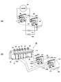
- FIG. 1 is a partial perspective view showing the shapes of the positive electrode terminals (162 and 172) and the negative electrode terminals (167 and 177) of the battery pack 100, and is a diagram showing a connection circuit at the time of high voltage output, and (B) is a view showing a high voltage. It is a partial perspective view for showing the connection state of the terminal part 50 of an electric device, and the terminal of a battery pack 100 side.
- FIG. 14 It is a top view which shows the state which removed the module for wireless communication in the circuit board 150 of FIG. 14 is a cross-sectional view taken along the line AA of the circuit board 150 of the battery pack 100 of FIG. It is a front view of the circuit board 150 of the battery pack 100 of FIG. It is a figure which shows the silicon coating state to the circuit board 150 of the battery pack 100 which concerns on this invention. It is a perspective view of the formwork 281 of FIG. It is a figure which shows the silicon coating state to the circuit board 150 by the method different from FIG.
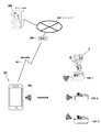
- FIG. 1 is an overall schematic view of a management system using the battery pack 100 according to the embodiment of the present invention.
- the power tool main body 1 is a portable electric device that can use the battery pack 100-1 as a power source, and is an impact tool that has been widely used in the past.
- the battery pack 100 of this embodiment is equipped with a microcomputer internally, and is equipped with Bluetooth (Bluetooth: Bluetooth SIG, a registered trademark of Inc. USA) that enables proximity wireless communication with the microcomputer. Since the wireless communication device is mounted inside the battery pack 100 in this way, bidirectional wireless communication between the battery packs 100-1 to 3 with the terminal device 301, which is an external device, becomes possible.
- the terminal device 301 can also communicate with the battery pack 100-1 attached to the power tool body 1, and the battery packs 100-2 and 100 removed from the electric device such as the power tool body 1. Communication with -3 is also possible.
- the terminal device 301 can transmit the information received from the battery packs 100-1 to 3 to the server device of the support company 300, and also receives some information from the terminal device 301 and displays it on the display screen 302. can do. Furthermore, it is possible to perform wireless communication with a specific battery pack (for example, 100-2) using a wireless communication device and write information to the microcomputer of the battery pack 100-2.
- a specific battery pack for example, 100-2
- the battery pack 100 (for example, 100-1) is paired with the terminal device 301.
- "Pairing” is a work of associating and registering the terminal device 301 and the battery pack 100 side by using wireless communication, and by performing these registration work (pairing), the terminal device 301 is paired. Necessary information can be obtained from the battery pack 100.
- all the battery packs that can be wirelessly connected may be paired at the same time, but it is not always necessary to perform all of them at the same time, and only the target battery pack 100 whose status is to be checked should be selected and paired. You may.
- the terminal device 301 processes the information received from the battery pack 100 by wireless communication, and records the state of the battery pack 100, particularly the number of times of charging, the number of times of overcharging, the number of times of overdischarging, the type of the attached power tool, and the voltage recording during use. Acquire various usage conditions of the battery pack 100 and grasp the current state of the battery pack 100. The grasped information is transmitted to the support company 300 via the telephone communication network 361 and the network 350. Dedicated software, so-called application software, is installed in the terminal device 301 in order to enable wireless communication with the battery pack 100.
- the terminal device 301 is not limited to a so-called smartphone, and can be a tablet-type PC (Personal Computer) or a general-purpose device as long as it can perform two-way or one-way wireless communication with the wireless communication device on the battery pack 100 side. It may be a PC or the like.
- a tablet-type PC Personal Computer
- PC Personal Computer
- FIG. 2 is a perspective view of the battery pack 100 according to the embodiment of the present invention.
- This battery pack 100 accommodates two sets of cell units in which five 3.6V lithium-ion battery cells are connected in series, and by changing the connection method of the two sets of cell units, it has an 18V output (low voltage output). It is a "variable voltage battery pack" that can switch between both 36V output (high voltage output).
- the housing of the battery pack 100 is formed by a lower case 101 and an upper case 110 that can be divided in the vertical direction.
- the upper case 110 is formed with a mounting mechanism in which two rails 138a and 138b are formed for mounting on the battery pack mounting portion 2c (described later in FIG. 3) of the power tool main body 1.
- the rails 138a and 138b are formed so as to extend in a direction parallel to the mounting direction of the battery pack 100 and to project to the left and right side surfaces of the upper case 110.
- the slot 121 on the right side of the battery pack 100 near the rail 138a serves as an insertion port for the positive electrode terminal (C + terminal) for charging
- the slot 122 serves as an insertion port for the positive electrode terminal (+ terminal) for discharging.
- the slot 127 on the left side near the rail 138b serves as an insertion port for the negative electrode terminal (-terminal).
- a plurality of signal terminals for transmitting signals to the battery pack 100, the power tool main body 1 and an external charging device (not shown) are arranged, and here, four signal terminals are arranged.
- Slots 123-126 are provided between the power terminals.
- Slot 123 is a spare terminal insertion slot, and no terminal is provided in this embodiment.
- the slot 124 is an insertion port for a T terminal for outputting a signal serving as identification information of the battery pack 100 to the power tool main body or the charging device.
- Slot 125 is an insertion slot for a V terminal for inputting a control signal from an external charging device (not shown).
- the slot 126 is an insertion port for an LS terminal for outputting battery temperature information by a thermistor (temperature sensitive element) (not shown) provided in contact with the cell.
- a slot 128 for the LD terminal which outputs an abnormal stop signal by the battery protection circuit (not shown) included in the battery pack 100 is further provided. ..
- a raised portion 132 formed so as to be raised is formed on the rear side of the upper surface 115.
- a recessed stopper 131 is formed near the center of the raised 132.
- the stopper portion 131 becomes a contact surface when the battery pack 100 is mounted on the battery pack mounting portion 2c (described later in FIG. 3).
- the battery pack 100 is mounted at a predetermined position on the power tool body 1, the plurality of terminals (device side terminals) arranged on the power tool body 1 come into contact with the plurality of connection terminals arranged on the battery pack 100. It becomes a conductive state.
- An identification notch 111a is formed at the front left corner of the lower surface 111 so that the conventional 18V battery pack cannot be attached to the 36V power tool body.
- FIG. 3 is a perspective view of the power tool main body 1 to which the battery pack 100 according to the present invention is mounted.
- the power tool main body 1 shown here is an impact driver, and a handle portion 2b extending downward from the body portion of the housing 2 is provided, and a battery pack mounting portion 10 is formed below the handle portion 2b.
- a trigger switch 4 is provided on the handle portion 2b.
- An anvil (not shown) serving as an output shaft is provided on the front side of the housing 2, and a tip tool holding portion 8 for mounting the tip tool 9 is provided at the tip of the anvil.
- a Phillips screwdriver bit is attached as the tip tool 9.
- the terminal portion 20 is formed with a vertical surface 20a and a horizontal surface 20b which are abutting surfaces in the mounting direction (front-rear direction), and the horizontal surface 20b is adjacent to or faces the upper surface 115 (see FIG. 2) when the battery pack 100 is mounted. It becomes the surface to do.
- a curved portion 12 that comes into contact with the raised portion 132 (see FIG. 2) of the battery pack 100 is formed on the front side of the horizontal plane 20b, and a protruding portion 14 is formed near the center of the left and right sides of the curved portion 12.
- the protrusion 14 also serves as a boss for screwing the housing of the power tool body 1 formed in two in the left-right direction, and also serves as a stopper that limits the relative movement of the battery pack 100 in the mounting direction.
- FIG. 4 is a developed perspective view of the battery pack 100 of FIG.
- the housing of the battery pack 100 is formed by an upper case 110 and a lower case 101 that can be separated in the vertical direction, and 10 battery cells are housed in the internal space of the lower case 101.
- a plurality of battery cells (not shown) are fixed by a separator 245 made of a non-conductor such as synthetic resin in a state where five batteries are stacked in two stages.
- the separator 245 holds a plurality of battery cells so that only the left and right sides, which are both ends of the battery cells, are open.
- a circuit board 150 is fixed on the upper side of the separator 245 so as to cover the lithium ion battery cell.
- the circuit board 150 fixes a plurality of connection terminals (161, 162, 164 to 168, 171, 172, 177) by soldering, and electrically connects these connection terminals to a circuit pattern (not shown).
- the circuit board 150 is further equipped with various electronic elements (not shown here) such as a battery protection IC, a PTC thermistor, a resistor, a capacitor, a fuse, and a light emitting diode.
- a communication module and an antenna (both described later) forming a wireless communication device are mounted in the area occupied by the dotted line 152.
- the positive electrode terminals (161, 162, 171 and 172) and the negative electrode terminals (167, 177) are arranged at locations far apart in the left-right direction, and three signal terminals (T terminal 164, V terminal 165, and so on) are located between them.
- the LS terminal 166) is provided.
- a total of two sets of arms extending in the horizontal direction are provided, one set on the upper left and right and one set on the lower left and right.
- the LD terminal 168 is provided on the left side of the negative electrode terminal pair (167, 177).
- the lower case 101 has a substantially rectangular parallelepiped shape with an open upper surface.
- a slit 104 is provided substantially in the center of the front wall.
- the slit 134 of the upper case 110 is used as an inflow port for allowing the cooling air sent from the charging device side to flow into the internal space of the battery pack 100 when charging with the charging device, and the slit 104 of the lower case 101. Is used as a cooling air outlet.
- the output from the battery cell side is connected to the circuit board 150 via the drawing tabs 261a, 266a, 271a, 276a for connection extending upward in a plate shape. Further, the end portions 294b, 296b to 299b of the lead wire from the intermediate connection point of the battery cells connected in series are arranged so as to extend upward and are soldered on the circuit board. Further, the intermediate drawer tabs 262a and 263a from the intermediate connection points of the battery cells connected in series are arranged so as to extend upward so as to be connected to the circuit board 150. Screw bosses 247a and 247b for fixing the circuit board 150 are formed on the upper side of the separator 245.
- FIG. 5 is a partial view of the circuit board 150 of the battery pack 100, in which a positive electrode terminal pair (upper positive electrode terminal 162 and lower positive electrode terminal 172) fixed to the circuit board 150 and a negative electrode terminal pair (upper negative electrode terminal 167 and lower) are shown. Only the side negative electrode terminal 177) is shown.
- FIG. 5A is a partial perspective view showing the shapes of the positive electrode terminals (162 and 172) and the negative electrode terminals (167 and 177) of the battery pack 100 of this embodiment, and a diagram showing a connection circuit at the time of high voltage output.
- FIG. 5 is a partial view of the circuit board 150 of the battery pack 100, in which a positive electrode terminal pair (upper positive electrode terminal 162 and lower positive electrode terminal 172) fixed to the circuit board 150 and a negative electrode terminal pair (upper negative electrode terminal 167 and lower) are shown. Only the side negative electrode terminal 177) is shown.
- FIG. 5A is a partial perspective view showing the shapes of the positive electrode terminals (162 and 172) and the negative electrode terminals (
- FIG. 5B is a partial perspective view showing a connection state between the terminal portion 50 of the high-voltage electric device and the terminal on the battery pack 100 side.
- the upper positive electrode terminal 162 and the lower positive electrode terminal 172 are arranged side by side in the slot 122 (see FIG. 2) of the battery pack 100.
- the upper positive electrode terminal 162 and the lower positive electrode terminal 172 are formed by pressing a metal plate, and the legs are firmly fixed to the circuit board 150 by soldering or the like.
- the upper positive electrode terminal 162 and the lower positive electrode terminal 172 are arranged at a distance from each other and are in an electrically non-conducting state.
- the slot 127 see FIG.
- the upper negative electrode terminal 167 and the lower negative electrode terminal 177 are arranged side by side.
- the upper positive electrode terminal 162 and the upper negative electrode terminal 167 are the same metal component, and the lower positive electrode terminal 172 and the lower negative electrode terminal 177 are the same metal component.
- an upper cell unit (first cell unit) 146 and a lower cell unit (second cell unit) 147 in which five lithium ion battery cells are connected in series are housed, and the upper cell unit is accommodated.
- the positive electrode of 146 is connected to the upper positive electrode terminal 162 corresponding to the first positive electrode terminal
- the negative electrode of the upper cell unit 146 is connected to the lower negative electrode terminal 177 corresponding to the first negative electrode terminal.
- the positive electrode of the lower cell unit 147 is connected to the lower positive electrode terminal 172 corresponding to the second positive electrode terminal
- the negative electrode of the lower cell unit 147 is connected to the upper negative electrode terminal 167 corresponding to the second negative electrode terminal.
- the positive electrode input terminal on the power tool body 1 side is connected to the upper positive electrode terminal 162
- the negative electrode input terminal is connected to the upper negative electrode terminal 167
- the lower side is shown by the dotted line 59. If the side positive electrode terminal 172 and the lower negative electrode terminal 177 are electrically connected, the output of the series connection of the upper cell unit 146 and the lower cell unit 147, that is, the rating of 36 V is from the battery pack 100 to the load device 70 of the power tool body 1. Will be output to.
- the negative electrode terminal pair also has the same shape as the positive electrode terminal pair, and is composed of an upper negative electrode terminal 167 and a lower negative electrode terminal 177, and these negative electrode terminal pairs (167, 177) are arranged inside a single slot 127. To. These are a plurality of terminals (167, 177) arranged close to each other, and function as a group of switching terminals used for voltage switching. Inside the slot 127, the arm assembly of the upper negative electrode terminal 167 is arranged on the upper side, and the arm assembly of the lower negative electrode terminal 177 is arranged on the lower side of the arm assembly of the upper negative electrode terminal 167. Although not shown in FIG.
- the positive electrode terminal pair for charging (upper positive electrode terminal 161 and lower positive electrode terminal 172) is on the right side. 171: (see FIG. 4) is arranged.
- the shape of the positive electrode terminal pair (161, 171) for charging is the same as that of the upper positive electrode terminal 162 and the lower positive electrode terminal 172.
- FIG. 5B is a diagram showing a connection relationship between the terminal portion 50 of the power tool main body 1 having a rating of 36 V and the connection terminals (162, 167, 172, 177) on the battery pack 100 side.
- the terminal portion 50 is provided in the battery pack mounting portion 2c of the power tool main body 1.
- the terminal section 50 is provided with device-side terminals (52, 59a, 54 to 56, 57, 59b, 58) corresponding to slots 121 to 128 (see FIG. 2) of the battery pack 100, and is made of a synthetic resin base. It is fixed so as to be cast in 51.
- the upper connection terminal portion of the base 51 and the lower plate-shaped terminal portion having the same reference numeral are composed of an electrically conductive metal plate.
- the device-side terminal is not provided at the position corresponding to the slot 123 (see FIG. 2).
- a positive electrode input terminal 52 for receiving power and a negative electrode input terminal 57 are provided in a small size above the short circuit terminals 59a and 59b.
- the positive electrode input terminal 52 and the short-circuit terminal 59a are not conducting with each other.
- the negative electrode input terminal 57 and the short-circuit terminal 59b are not conducting with each other.
- the positive electrode input terminal 52 is fitted only to the upper positive electrode terminal 162, and the negative electrode input terminal 57 is fitted only to the upper negative electrode terminal 167.
- the terminal portion 50 of the power tool main body 1 is provided with small terminals 59a and 59b for short-circuiting the lower positive electrode terminal 172 and the lower negative electrode terminal 177.
- the small terminals 59a and 59b are both end portions of the short circuit 59 and are connected inside the base 51.
- the positive electrode input terminal 52 is a portion that fits with the upper positive electrode terminal 162 and connects the terminal portion formed in a flat plate shape to the circuit board side of the power tool main body 1 side, and is a base 51. It is composed of terminals that protrude upward.
- the positive electrode input terminal 52 is cast into a base 51 made of synthetic resin.
- the negative electrode input terminal 57 is also the same as the positive electrode input terminal 52, and the height of the terminal is set to be slightly smaller than half of the other terminal portions (54 to 56, 58).
- the other terminal portions (54 to 56, 58) are terminals for signal transmission.
- Recesses 51a and 51b for being sandwiched by the housing are provided on the front side and the rear side of the synthetic resin base 51 of the terminal portion 50.
- the positive electrode input terminal 52 and the short-circuit terminal 59b are the same when the battery pack 100 is relatively moved with respect to the power tool main body 1 along the insertion direction. It is inserted all the way through the slot 122 (see FIG. 2) and fitted into the upper positive electrode terminal 162 and the lower positive electrode terminal 172, respectively. At this time, the positive electrode input terminal 52 is press-fitted between the arms 162a and 162b of the upper positive electrode terminal 162 so as to spread between the fitting portions of the upper positive electrode terminal 162, and the short-circuit terminal 59b is formed on the lower positive electrode terminal 172. It is press-fitted so as to spread between the arms 172a and 172b.
- the negative electrode input terminal 57 and the short-circuit terminal 59b are inserted into the inside through the same slot 127 (see FIG. 2), and are fitted into the upper negative electrode terminal 167 and the lower negative electrode terminal 177, respectively.
- the negative electrode input terminal 57 is press-fitted between the arm portions 167a and 167b of the upper negative electrode terminal 167 so as to spread between the fitting portions.
- the short-circuit terminal 59b is press-fitted so as to spread between the arm portions 177a and 177b of the lower negative electrode terminal 177.
- the output of the series connection of the upper cell unit 146 and the lower cell unit 147 that is, the rated 36V is output from the battery pack 100.
- FIG. 6 (A) and 6 (B) are diagrams showing a connection state when the battery pack 100 of this embodiment is attached to the power tool main body 1 (see FIG. 3) for 18 V.
- the terminal portion of the positive electrode input terminal 82 is fitted and press-fitted so as to spread both the upper positive electrode terminal 162 and the open end portion of the lower positive electrode terminal 172.
- a part of the upper side of the terminal portion of the positive electrode input terminal 82 comes into contact with the upper positive electrode terminal 162, and a part of the lower side comes into contact with the lower positive electrode terminal 172.
- the two positive electrode terminals (162 and 172) are fitted. Is short-circuited.
- the terminal portion of the negative electrode input terminal 87 is fitted and press-fitted so as to push out both the upper negative electrode terminal 167 and the open end portion of the lower negative electrode terminal 177, and the upper portion of the terminal portion of the negative electrode input terminal 87. Region is in contact with the upper negative electrode terminal 167, and a part of the lower region is in contact with the lower negative electrode terminal 177.
- the two negative electrode terminals (167 and 177) are fitted. Is short-circuited, and the output of the parallel connection of the upper cell unit 146 and the lower cell unit 147, that is, the rated value of 18V is output to the power tool main body 1.
- the battery pack 100 of this embodiment can be attached to either the power tool main body 1 for 18V (see FIG. 3) or the power tool main body for 36V (not shown) to form the battery pack 100.
- the output switches automatically. Since this voltage switching is not performed on the battery pack 100 side but automatically depending on the shape of the terminal portion on the power tool main body 1 side, there is no possibility that a voltage setting error will occur. Further, since it is not necessary to provide a dedicated voltage switching mechanism such as a mechanical switch on the battery pack 100 side, the structure is simple, the risk of failure is low, and a long-life battery pack can be realized.
- the battery pack 100 When the battery pack 100 is charged using an external charging device (not shown), it can be charged with the same charging device as the conventional 18V battery pack. Since the slot 121 of the battery pack 100 is provided with a positive electrode terminal for charging having the same shape as the upper positive electrode terminal 162 and the lower positive electrode terminal 172, the positive electrode terminal for charging (162, 172) is replaced with the positive electrode terminal for charging.
- the positive electrode terminal (not shown) may be connected to the positive electrode terminal of the external charging device (not shown).
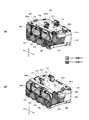
- the separator 245 (see FIG. 4) is formed by stacking five battery cells 146a to 146e and 147a to 147e in two upper and lower stages.
- FIG. 7 shows a state in which the battery cells 146a to 146e and 147a to 147e are pulled out from the separator 245, but at the time of assembly, they are inserted into the cylindrical space 246 of the separator 245 and between the terminals exposed on both the left and right sides of the separator.
- connection plates 262 to 265 and 272 to 275 are connected to each other, and the drawer plates 261 to 266, 271 and 276 are connected to the battery cell. After that, insulating sheets 278a and 278b are attached on the connecting plates 262 to 265, 272 to 275 and the drawer plates 261 and 266, 271 and 276 for insulation.
- the axes of the battery cells are stacked so as to be parallel to each other, and the directions of the adjacent cells are arranged so as to be alternately reversed, and the positive electrode terminal and the negative electrode terminal of the adjacent battery cells are connected to the metal connection plates 262 to It is connected using 265, 272 to 275.
- the terminals on both sides of the battery cell and the connection plates 262 to 265 and 272 to 275 are fixed by spot welding at a plurality of locations.
- the five series-connected battery cells installed in the upper stage form the upper cell unit 146 (detailed in FIG. 9), and the five series-connected battery cells installed in the lower stage are below.
- the side cell unit 147 (detailed in FIG. 9) is formed.
- lithium ion battery cells (not shown) having a diameter of 18 mm and a length of 65 mm that can be charged and discharged multiple times, which are called 18650 size, are used, but the size and number of battery cells are arbitrary.
- Two electrodes are provided at both ends of the battery cell in the length direction. Of the two electrodes, one is the positive electrode and the other is the negative electrode.
- the positive electrode of the upper cell unit 146 is connected to the circuit board 150 using a drawer plate 261 on which the drawer tab 261a is formed, and the negative electrode of the upper cell unit 146 is a circuit using the drawer plate 266 on which the drawer tab 266a is formed. It is connected to the substrate 150.
- the positive electrode of the lower cell unit 147 is connected to the circuit board 150 by using the drawer plate 271 on which the drawer tab 271a is formed, and the negative electrode of the lower cell unit 147 is the drawer plate on which the drawer tab 276a is formed. It is connected to the circuit board 150 using 276.
- tab holders 250 to 252 and 255 to 257 for holding the tabs of the drawer plates 261, 266, 271, and 276 in the shape of a bent metal thin plate are formed.
- the tab holders 250 to 252 and 255 to 257 are tab holding portions formed to hold the drawer tabs 261a, 262a, 263a, 266a, 271a, and 276a bent in an L shape, and are seated when the separator 245 is formed. It is integrally molded as a recess having a surface, a back surface, and both side surfaces, and drawer tabs 261a, 262a, 263a, 266a, 271a, and 276a are fitted into the recess, respectively.
- Two screw bosses 247a and 247b for screwing the circuit board 150 are formed on the upper portion of the separator 245.
- the right side of the drawer plates 261, 271 and the connecting plate 263, 265, 273, 275 is covered with the insulating sheet 278a, and the left side of the drawer plate 266, 276 and the connecting plate 262, 264, 272, 274 is covered with the insulating sheet 278b.
- the insulating sheet 278a is made of a material that does not conduct electricity, and a sealing material is applied to the inner portion thereof.
- FIG. 8 is a circuit diagram of a power tool main body (high-voltage electric device) 1 on which the battery pack 100 is mounted, and has a configuration in which a short-circuit circuit (short-circuit path) 59 is incorporated in the power tool main body 1.
- the right side is the battery pack 100, and here, only the necessary configurations are extracted and shown for ease of explanation.
- a short circuit 59 shown by a thick wire is provided in the terminal portion 50 on the power tool main body 1 side.
- the short-circuit circuit 59 can be composed of a short-circuit element made of a metal plate, and as shown in FIG.
- a U-shape is formed on a synthetic resin base 51 together with other device-side terminals such as a positive electrode input terminal 52 and a negative electrode input terminal 57. It can be constructed by casting a metal plate bent into a shape. One end of the U-shaped bent metal plate serves as a short-circuit terminal 59a, and the other end serves as a short-circuit terminal 59b. By simply mounting the battery pack 100 on the terminal portion 50 having such a shape, DC power rated at 36 V is supplied to the positive electrode input terminal 52 and the negative electrode input terminal 57.
- the power tool main body 1 includes a microcomputer 60 for controlling the rotation of the motor 3.
- the driving voltage (5V or 3.3V) of the microcomputer 60 is supplied by the power supply device 61 that inputs the voltage across the short-circuit terminal 59a and the negative electrode input terminal 57.
- the battery pack 100 of the present embodiment having two positive electrode terminals (162, 172) and two negative electrode terminals (167, 177) can be obtained.
- a series connection circuit of the upper cell unit 146 and the lower cell unit 147 can be established only by mounting.
- FIG. 9 is a block diagram showing an internal circuit of the battery pack 100 of this embodiment.
- the battery pack 100 includes an upper positive electrode terminal (upper +) 162, a lower positive electrode terminal (lower +) 172, an upper negative electrode terminal (upper-) 167, and a lower negative electrode terminal (lower). +) Consists of 177.
- the battery pack 100 is provided with other signal terminal groups (T terminal, V terminal, LS terminal, LD terminal), but their illustrations are omitted here.
- the output of the upper cell unit 146 is connected to the upper positive electrode terminal 162 and the lower negative electrode terminal 177. That is, the positive electrode (+ output) of the upper cell unit 146 is connected to the upper positive electrode terminal 162, and the negative electrode ( ⁇ output) of the upper cell unit 146 is connected to the lower negative electrode terminal 177.
- the positive electrode (+ output) of the lower cell unit 147 is connected to the lower positive electrode terminal 172, and the negative electrode ( ⁇ output) of the lower cell unit 147 is connected to the upper negative electrode terminal 167.
- Protection ICs 180 and 190 for monitoring the voltage of the battery cell are connected to the upper cell unit 146 and the lower cell unit 147, respectively, and the microcomputer 154 is connected to these protection ICs 180 and 190, respectively.
- the protection IC 180 executes a cell balance function, a cascade connection function, and a disconnection detection function in addition to an overcharge protection function and an overdischarge protection function by inputting a voltage across each battery cell of the upper cell unit 146. It is an integrated circuit commercially available as a "protection IC for a lithium ion battery".
- the protection IC 180 when the voltage of the battery cell of the upper cell unit 146 drops below a predetermined value and becomes an over-discharged state, the protection IC 180 outputs a signal (high signal) 183 indicating over-discharge to the microcomputer 154 to output the upper side.
- a signal (high signal) 184 indicating overcharge is output to the microcomputer 154.
- a protective IC 190 is connected to the lower cell unit 147.
- a microcomputer (Micro Controller Unit) 154 is connected in the circuit of the lower cell unit 147, that is, in the circuit between the lower positive electrode terminal 172 and the upper negative electrode terminal 167.
- the output from the protection IC 180 (overdischarge signal 183, overcharge signal 184) and the output from the protection IC 190 (overdischarge signal 191 and overcharge signal 192) are input to the microcomputer 154.
- the microcomputer 154 includes, for example, a voltage detection circuit called an analog front end (AFE), and measures the current value flowing from the output voltage of the current detection circuit 193 to the lower cell unit 147.
- AFE analog front end
- the power supply for driving the microcomputer 154 is generated by the power supply circuit 185 connected to the lower cell unit 147, and the power supply voltage (VDD1) is supplied to the microcomputer 154.
- a shunt resistor 194 for measuring the current value is provided on the ground side of the lower cell unit 147.
- the microcomputer 154 monitors the current value and the cell temperature, and also monitors the states of the upper cell unit 146 and the lower cell unit 147 to integrate and control the operating status of both. Further, when the power tool main body 1 needs to be stopped urgently, a discharge prohibition signal is sent to the electric device main body side via an LD terminal (not shown).
- the protection IC 190 monitors the voltage of the battery cell in the lower cell unit 147, and sends an over-discharge signal 191 to the microcomputer 154 when it detects a state in which the voltage drops to a predetermined lower limit value (over-discharge state).
- the microcomputer 154 includes a timer circuit and a storage device as well as a microprocessor (not shown). The microcomputer 154 stores the monitored battery voltage, temperature, and count value of the number of times of charging in the storage device.
- a wireless communication circuit 155 is connected to the microcomputer 154.
- An antenna 156 is connected to the wireless communication circuit 155.
- a commercially available wireless communication module 153 is used and mounted on the circuit board 150.
- the wireless communication module 153 is a combination of a wireless communication circuit 155 and an antenna 156 mounted on a common base (not shown).
- the wireless communication module 153 or the antenna 156 corresponds to the wireless communication unit in the present invention.
- the protective IC 190 detects that the voltage of the battery cell exceeds a predetermined upper limit value, and causes an overcharged state.
- the indicated overcharge signal 192 is sent to the microcomputer 154.
- the microcomputer 154 stores the information in the storage device, and sends a charge stop signal to a charging device (not shown) via an LS terminal (not shown).
- the power supply circuit 185 uses the electric power of the lower cell unit 147 to generate a power supply for operating the microcomputer 154.
- a power supply circuit 185 for the microcomputer 154 was provided on the lower stage side, and the microcomputer 154 was provided in the circuit of the lower cell unit 147.
- the microcomputer 154 can switch between holding and releasing the power supply voltage (VDD1) applied to itself, and has a normal operation state (normal mode) and an operation stop state (so-called sleep mode).
- the output of the upper voltage detection circuit 182 connected to the upper positive electrode terminal 162 is input to the microcomputer 154.
- This output indicates the potential of the upper cell unit 146 when the battery pack 100 is not mounted on the power tool body 1 or an external charging device (not shown).
- the upper positive electrode terminal 162 and the lower positive electrode terminal 172 are connected, so that the positive electrodes of the upper cell unit 146 and the lower cell unit 147 are respectively connected.
- the potentials are the same, and each negative electrode has the same potential. From this, the microcomputer 154 compares the potential of the upper positive electrode terminal 162 with the potential of the lower positive electrode terminal 172 to determine whether the battery pack 100 is not mounted or is mounted on the low voltage device main body.
- the microcomputer 154 In order to detect the potential of the lower positive electrode terminal 172, it is preferable to configure the microcomputer 154 to acquire the positive electrode potential of the uppermost battery cell 147a among the battery cells in the lower cell unit 147.
- a situation in which the power supply from the battery pack 100 must be stopped for example, an excessive current during discharging, a decrease in cell voltage during discharging (over-discharging), and an abnormal increase in cell temperature (excessive).
- a temperature or the like occurs, the operation of the power tool main body 1 can be stopped quickly by transmitting an LD signal to the power tool main body side via the microcomputer 154.
- FIGS. 10A and 10B are side views of the separator 245 after assembling the parts shown in FIG. 5, where FIG. 10A is a right side view and FIG. 10B is a left side view.
- FIG. 10A is a right side view
- FIG. 10B is a left side view.
- the connection terminal group for ease of explanation, only two sets of the positive electrode terminal (162, 177) for discharging and the negative electrode terminal (167, 177) are shown as the connection terminal group, and the other connection terminals (161, 164 to The illustration of 166, 168, 171) is omitted.
- the resin layer on the circuit board 150 shows the situation before being formed.
- the upper cell unit 146 is composed of battery cells 146a to 146e arranged on the upper stage side, and has a drawer tab 261a extending upward from the drawer plate 261 on the positive electrode side and a drawer tab 266a extending upward from the drawer plate 266 on the negative electrode side. It is connected to the circuit board 150.
- a slit-shaped through hole (not shown) is formed in the circuit board 150, and the through hole is passed through from the lower side to the upper side so that the upper portion of the drawer tabs 261a and 266a is exposed from the surface of the circuit board 150 to the upper side. .. By soldering that portion, the circuit board 150 and the drawer tabs 261a and 266a are electrically connected.
- the lower cell unit 147 is composed of battery cells 147a to 147e arranged on the lower stage side, and is circuited by drawer tabs 271a and 276a for connection extending upward from the drawer plates 271 and 276 provided at both ends. It is connected to the substrate 150.
- a slit-shaped through hole (not shown) is formed in the circuit board 150, and the through hole is passed through from the lower side to the upper side so that the upper portion of the drawer tabs 271a and 276a is exposed from the surface of the circuit board 150 to the upper side. .. By soldering that portion, the circuit board 150 and the drawer tabs 271a and 276a are electrically connected.
- a slit-shaped through hole (not shown) is formed in the circuit board 150, and the through hole is passed through from the lower side to the upper side, and the upper part of the intermediate drawer tabs 262a and 263a is exposed from the surface of the circuit board 150 to the upper side. To do.
- the intermediate drawer tabs 262a and 263a are fixed by soldering to the circuit board 150.
- the width (distance in the front-rear direction) of the intermediate drawer tabs 262a and 263a is formed to be smaller than the width (length in the front-rear direction) of the drawer tab 261a of FIG. 10A and the drawer tab 266a of FIG.
- drawer tabs 261a, 266a, 271a, 276a are terminals for power output and high voltage and large current flow, while the intermediate drawer tabs 262a and 263a are connected for measuring the intermediate potential. This is because it is a terminal that is used and only a small amount of current flows. It is also possible to form an intermediate drawer tab on the other connecting plate 264 and the connecting plate 265 provided on the upper side. However, here, due to the formation of the wiring pattern, it is decided to provide the connection terminals 264a and 265a and connect them to the circuit board 150 with lead wires (not shown).
- connection terminals 272a to 275a are provided and the lead wires 296 to 299 are connected to the circuit board 150. I made it.
- FIG. 11 is a perspective view showing a state in which the circuit board 150 is fixed to the separator 245, and shows a state seen from the upper left front.
- the upper portions of the tabs 261a, 266a, 271a, and 276a are exposed upward from the surface of the circuit board 150 through the slit-shaped through holes 159a to 159d in the circuit board 150. By soldering the exposed parts of those tabs, the circuit board 150 and the drawer tabs 261a, 266a, 271a, and 276a are electrically connected.
- the battery cells 146a to 146e of the upper cell unit 146 are directly connected to the circuit board 150, and the battery cells 147a to 147e of the lower cell unit 147 are directly connected to the circuit board 150.
- lead wires 296 to 299 for measuring the potentials of the connection plates 262 to 264 and the connection plates 272 to 274 are connected.
- the ends of the lead wires shown in FIG. 4 294b, 296b, 297b, 298b, 299b are soldered to the circuit board 150.
- the connection plates 262 and 263 (see FIG. 12) that are close to the circuit board 150 are bent in an L shape and are directly connected to the circuit board 150 by using the intermediate drawer tabs 262a and 263a in which the vertical plate portion extends upward. To.
- the drawer tabs 261a and 266a for the output (+ output,-output) of the upper cell unit 146 are shaped so as to have a substantially L shape in front view or rear view, and the longitudinal direction thereof is a substantially rectangular circuit board 150. Arranged so as to be parallel to the long side.
- the surface fixed to the terminal of the battery cell of the drawer plates 261 and 266 is extended upward and bent inward, and the upper surface of the separator is slightly extended inward in the horizontal direction and upward at an appropriate position. It is a bent body of a thin metal plate in which the bent vertical wall portion is made into drawer tabs 261a and 266a by bending in an L shape.
- the drawer plate 271 from the terminal surface 271b of the lower cell is extended forward and then bent at a right angle to the left side to form the side surface portion 271c. Extend upwards. That is, the drawer plate 271 is extended upward by crawling the side surface on the short side in the top view of the separator 245, and bent from the front side surface to the rear side of the separator 245 to form the horizontal plane portion 271d, and the horizontal plane portion 271d is on the upper side.
- a drawer tab 271a was formed by extending the tabs at right angles to the surface.
- the drawer tab 271a is soldered by penetrating a slit-shaped through hole 159c formed in the circuit board 150 from the back surface to the front surface.
- the drawer tabs 271a and 276a are arranged so that the longitudinal direction is parallel to the short side of the substantially rectangular shape.
- the drawer plate 276 from the lower negative terminal is also pulled out in the same manner (see FIG. 12 described later), and is pulled out to the drawer tab 276a.
- the drawer plate 271 was further formed with a portion in which the width of the connection path was greatly narrowed, that is, a fuse portion 271e.
- the fuse portion 271e has a cutout portion 271f formed from the right side of the drawer plate 271 and a cutout portion 271 g formed from the left side to sufficiently narrow the width (horizontal width) of the remaining portion, and the drawer plate 271 is formed by this portion.
- a similar fuse function is similarly provided in the vicinity of the drawer tab 261a of the drawer plate 261 (see FIG. 12) from the positive terminal of the upper cell unit 146.
- the oval connecting plates 262, 264, 273, and 274 for connecting the electrodes of adjacent battery cells are formed of a thin metal plate such as stainless steel, and are fixed by spot welding to the battery cells. Will be done.
- the upper cell unit 146 is provided with a drawer tab 261a for positive output and a drawer tab 266a for negative output. Further, the lower cell unit 147 is provided with a drawer tab 271a for positive output and a drawer tab 276a for negative output. In this embodiment, the installation positions of the drawer tabs 261a, 266a, 271a, and 276a are also devised.
- the left and right center lines of the circuit board 150 or the center lines of the positive electrode terminal pair (162, 172) and the negative electrode terminal pair (167, 177) are designated as the left and right center lines A1 indicated by dotted lines.
- a dotted line connects the two center positions of the center position between the legs of the upper positive electrode terminal 162 and the lower positive electrode terminal 172 and the center position between the legs of the upper negative electrode terminal 167 and the lower negative electrode terminal 177.
- the positive electrode drawer tab 261a of the upper cell unit 146 exists in the region where the legs of the upper positive electrode terminal 162 are located, and the lower positive electrode terminal
- the lead-out plate 271a of the positive electrode of the lower cell unit 147 was made to exist in the region where the legs of 172 are located.
- drawer tabs 261a and 271a By arranging the drawer tabs 261a and 271a in this way, the drawer tab 261a and the upper positive electrode terminal 162, and the drawer plate 271a and the lower positive electrode terminal 172 can be efficiently connected by a wiring pattern arranged on the circuit board 150.
- the drawer tab 276a of the negative electrode of the lower cell unit 147 exists in the region where the legs of the upper negative electrode terminal 167 are located, and the negative electrode of the upper cell unit 146 is located in the region where the legs of the lower negative electrode terminal 177 are located.
- Drawer tab 266a was made to exist. By arranging the drawer tabs 276a and 266a in this way, the upper negative electrode terminal 167 and the lower negative electrode terminal 177 can be efficiently connected by the wiring pattern arranged on the circuit board 150.
- FIG. 12 is a perspective view showing a state in which the circuit board 150 is fixed to the separator 245, and shows a state seen from the upper right rear.
- Recesses 150c and 150d for positioning the circuit board 150 with respect to the separator 245 are formed on the left and right edges near the center when viewed in the front-rear direction of the circuit board 150, and convex portions 245c and 245d formed on the separator 245 are formed therein.
- Engage Further, on the front side of the separator 245, an abutting portion 245e for holding the front end of the circuit board 150 is formed and abuts on the front edge portion of the circuit board 150.
- the drawer plate 261 is formed with a terminal surface 261b extending parallel to the electrode of the battery cell and a horizontal surface portion 261c bent in a direction perpendicular to the upper side of the separator 245 from the terminal surface 261b, and the horizontal surface portion 261c is moved upward.
- the drawer tab 261a was formed by extending it in a tab shape at a right angle.
- the fuse portion 261d is formed by forming a cutout portion 261e in which a part of the horizontal plane is largely cut out from the front side, thereby reducing the width (distance in the front-rear direction) of the fuse portion 261d.
- drawer plate 261 not only the drawer plate 261 but also the other drawer plates 266, 271 and 276 and the connection plates 262 to 265 and 272 to 275 are formed by pressing a thin plate such as stainless steel. Therefore, it is not necessary to add a separate fuse element to the upper cell unit 146 and the lower cell unit 147.
- FIG. 13 is a diagram for explaining a method of connecting the drawer plates 261, 266, 271, 276 of the battery pack 100 to the positive electrode terminals (162, 172) and the negative electrode terminals (167, 177).
- (A) is a view seen from the front side
- (B) is a view seen from the rear side.
- the drawer tab 261a which is the + output of the upper cell unit 146, is connected to the circuit board 150 by the region circle 2 on the rear side of the upper positive electrode terminal 162.
- the drawer tab 261a and the upper positive electrode terminal 162 can be linearly connected at a short distance.
- the drawer tab 266a which is the negative output of the upper cell unit 146, is connected to the circuit board 150 by the region circle 3 on the front side of the lower negative electrode terminal 177.
- the drawer tab 266a and the lower negative electrode terminal 177 can be linearly connected at a short distance.
- the drawer tab 271a which is the + output of the lower cell unit 147, is connected to the circuit board 150 by the region circle 1 on the front side of the lower positive electrode terminal 172. Therefore, as shown by the dotted line, the drawer tab 271a and the lower positive electrode terminal 172 can be linearly connected at a short distance.
- the drawer tab 276a which is the negative output of the lower cell unit 147, is connected to the circuit board 150 by the region circle 4 on the rear side of the upper negative electrode terminal 167. Therefore, as shown by the dotted line, the drawer tab 276a and the upper negative electrode terminal 167 can be linearly connected at a short distance. As described above, since the wiring for electric power can be linearly connected to the connection terminals (162, 167, 172, 177) like the four dotted lines shown on the circuit board 150, the wiring patterns intersect. It can be efficiently arranged on the circuit board as a thick wiring pattern without any problem.
- the connection from the battery cell to the output terminal group to the positive electrode terminals (162, 172) and the negative electrode terminals (167, 177) is realized in the wiring pattern on the circuit board 150. .. Therefore, it is preferable to install the wireless communication circuit and the wireless antenna at a position away from the wiring pattern. Then, there are only two places behind the installation location, one near the front short side of the rectangular circuit board 150 and near the center of the left and right, and the other near the short side behind the circuit board 150 and near the center of the left and right. There are no candidates.
- the wireless communication circuit and the antenna unit are mounted at the positions shown by the dotted line 152. By mounting in this position, it is on the back surface of the circuit board 150, at a position as far as possible from the connection terminal group having many metal parts, and as far as possible from the main power line (wiring for electric power). It was possible to install a wireless communication circuit. By arranging the antenna portion at the end of the circuit board 150, there is an effect of suppressing a decrease in antenna efficiency during wireless communication.
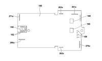
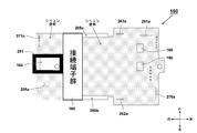
- FIG. 14 is a top view of the circuit board 150 of the battery pack 100 according to the present invention.
- the wireless communication module 153 is arranged in a square area in a top view.
- the wireless communication module 153 is formed by forming an antenna 156 on a resin base by a wiring pattern.
- a microcomputer 154 is provided at one end of the antenna 156, and a capacitor 157 is provided at the other end of the antenna 156. Is provided.
- the capacitor 157 is provided at the tip of the antenna 156 and is also used to solder the antenna 156 to the wiring pattern of the circuit board 150.
- the microcomputer 154 is a general-purpose microcomputer incorporating a Bluetooth (registered trademark) communication circuit, and here, information from the protection ICs 180 and 190 is aggregated by connecting to the protection ICs 180 and 190 for battery charge / discharge control. Then, while controlling the transmission of the LD signal and the LS signal to the mounted electric device main body and the charger, the state of the upper cell unit 146 and the lower cell unit 147 is monitored, and a storage device (nonvolatile memory) (not shown) is used. ) Periodically stores the state of the battery cell. Further, the microcomputer 154 enables communication by Bluetooth (registered trademark) in response to a pairing request from the outside, and here, communicates with an external terminal device 301 (see FIG. 1).
- Bluetooth registered trademark
- metal terminals 261a, 266a, 271a, and 276a of the positive electrode and the negative electrode through which a large current flowing by 18V DC or 36V DC flows are diagonally arranged. Further, as shown in FIG. 13, wiring from the metal terminals 261a, 266a, 271a, and 276a to the connection terminal group 160 is performed by a circuit pattern formed on the circuit board 150 (note that lead wires are used for these). The wiring that was there is fine). As described above, in the vicinity of the wireless communication module 153, there is a portion where a high voltage and a high current flow, and further, a large metal terminal is present, which hinders wireless communication.
- the wireless communication module 153 is substantially attached to the front side edge of the circuit board 150 with reference to the mounting direction of the battery pack 100. Placed in the center. Moreover, the antenna 156 is located in front of the microcomputer 154 and is arranged so as to be separated from the connection terminal group 160 as much as possible. With this arrangement, it is not necessary to cover the periphery of the antenna 156, particularly the front side, the upper side, and the lower side with a metal portion, so that radio waves are satisfactorily radiated from the antenna 156.
- the wireless communication module 153 is arranged near the center of the circuit board 150, for example, near the position indicated by the arrow 150b, the metal connection terminals are arranged on the front side, and the metal terminals extending from the battery cell on the right and left sides (intermediate).
- the mounted electric device is an impact tool as shown in FIG. 3
- the control circuit board (not shown) on the power tool body side is mounted on the upper side of the arrow 150b, and the radiation of radio waves is emitted. It is not preferable as an environment.
- the wireless communication module 153 is arranged near the center of the left and right at the rear edge of the circuit board 150.
- a switch unit for voltage check see 290 in FIG. 13
- five LEDs 158 are mounted in the vicinity of the rear mounting hole 151b. Therefore, the wireless communication module 153 cannot be mounted at that position.
- connection tabs from the battery cells are arranged in the regions on both the left and right sides. , The wireless communication module 153 is mounted in the central area.
- FIG. 15 is a top view showing a state in which the module for wireless communication is removed from the circuit board 150 of FIG.
- the difference from FIG. 14 shows the soldering pad (land) group 195 formed on the circuit board 150 with the wireless communication module 153 portion removed.
- the rear view of the wireless communication module 153 also has a shape corresponding to the connection pad group 195, and these are soldered by the reflow process.
- FIG. 16 is a sectional view taken along the line AA of the circuit board 150 of FIG.
- the microcomputer 154 is covered with a metal cover, and the wiring of the antenna 156 is sufficiently small compared to the cover. Therefore, considering the radiation of radio waves from the antenna 156, it is better to position the antenna 156 in front of the microcomputer 154.
- the control circuit of the battery cell including the protection IC 190 is arranged on the rear side of the connection terminal group 160.
- FIG. 17 is a front view of the circuit board 150 of the battery pack 100 of FIG. This figure also illustrates only the size of the wireless communication module 153 (microcomputer 154, antenna 156, capacitor 157) and the protection IC 180. From this figure, it can be understood that the antenna 156 is arranged so as to be in close contact with the circuit board 150.
- FIG. 18 is a diagram showing a silicon coating state of the battery pack 100 according to the present invention on the circuit board 150.
- a silicon resin layer is formed on almost all the upper surface of the circuit board 150 for dustproofing and waterproofing.
- Various formations of the silicon resin layer can be considered, and for example, it can be formed by coating.
- a silicon resin layer is also formed on the antenna, so that the silicon itself is a shield for radio wave radiation. There is a possibility that it can become.
- a waterproof wall is formed by the rubber mold 281 so that the inner portion of the mold 281 that becomes the waterproof wall is not coated with silicone resin.
- the mold 281 is integrally molded with rubber, and is positioned so as to be fitted into the outer frame portion of the microcomputer 154.
- the upper surface of the mold 281 comes into contact with the surface of the upper case 110 on the cell unit side, and is between the mold 281 and the upper case 110. It is configured so that there are no gaps. As a result, water and dust do not enter the antenna portion without applying the silicone resin to the antenna portion.
- the silicone resin is applied to the entire upper surface of the circuit board 150 as indicated by the wavy line hatching.
- the connection terminal group 160 is coated with resin only around the legs to be soldered.
- the rear side of the connection terminal group 160 is coated with resin on all parts except the left and right sides 285a and 285b, which do not need to be coated with resin.
- FIG. 19 is a perspective view of the mold 281 of FIG.
- the mold 281 is manufactured by integrally molding rubber, and is fitted into the antenna portion (antenna wire 156 and capacitor 157) and the outer frame portion of the microcomputer 154.
- a rubber sheet 282 may be further provided on the upper side of the mold 281. As a result, water and dust do not enter the antenna portion without applying the silicone resin to the antenna portion.
- the rubber sheet 282 may be fixed to the upper surface of the mold 281 by adhesion.
- FIG. 20 is a diagram showing a silicon coating state on the circuit board 150 by a method different from that of FIG.
- the sheet-shaped rubber 283 instead of limiting the front-back and left-right directions of the microcomputer 154 by the mold 281, covers not only the front-back and left-right directions of the microcomputer 154 but also the upper surface.
- a concave notch 283a is provided on the front edge of the rubber sheet 283 only around the antenna 156. At this time, waterproofness is ensured by attaching the edge of the notch 283a so as to be in close contact with the side surface of the shield covering the microcomputer 154.
- Silicone resin is applied around the rubber sheet 283, especially on the right side, left side, and rear side, but if it is difficult to apply it so that it is in close contact with the outer edge of the rubber sheet 283, as shown in FIG. 20, the outer edge portion 283b
- the resin is applied on the rubber sheet 283 so that the resin adheres to the upper side of the rubber sheet 283.
- the resin layer is formed by covering almost all the circuit boards 150 other than the wireless communication module 153 with silicon, the electronic elements mounted on the circuit board 150 are waterproofed. We were able to significantly improve the properties and dust resistance. Further, regarding the wireless communication module 153, since the antenna portion is not particularly covered with the resin, it is possible to eliminate the risk of deteriorating the radio wave radiation performance.
- the material of the resin layer is not limited to silicon, and other resins having excellent workability, waterproofness, and dustproofness may be used.
- Bluetooth registered trademark
- the present invention is not limited to the above-mentioned examples, and various modifications can be made without departing from the spirit of the present invention.
- Bluetooth registered trademark
- the present invention is not limited to the above-mentioned examples, and various modifications can be made without departing from the spirit of the present invention.
- Bluetooth registered trademark
- the present invention is not limited to the above-mentioned examples, and various modifications can be made without departing from the spirit of the present invention.
Landscapes
- Engineering & Computer Science (AREA)
- Mechanical Engineering (AREA)
- Battery Mounting, Suspending (AREA)
- Portable Power Tools In General (AREA)
Priority Applications (1)
| Application Number | Priority Date | Filing Date | Title |
|---|---|---|---|
| JP2021522222A JP7272430B2 (ja) | 2019-05-30 | 2020-05-15 | 電池パック及び電気機器 |
Applications Claiming Priority (2)
| Application Number | Priority Date | Filing Date | Title |
|---|---|---|---|
| JP2019101594 | 2019-05-30 | ||
| JP2019-101594 | 2019-05-30 |
Publications (1)
| Publication Number | Publication Date |
|---|---|
| WO2020241327A1 true WO2020241327A1 (ja) | 2020-12-03 |
Family
ID=73553446
Family Applications (1)
| Application Number | Title | Priority Date | Filing Date |
|---|---|---|---|
| PCT/JP2020/019539 Ceased WO2020241327A1 (ja) | 2019-05-30 | 2020-05-15 | 電池パック及び電気機器 |
Country Status (2)
| Country | Link |
|---|---|
| JP (1) | JP7272430B2 (https=) |
| WO (1) | WO2020241327A1 (https=) |
Cited By (3)
| Publication number | Priority date | Publication date | Assignee | Title |
|---|---|---|---|---|
| CN114603522A (zh) * | 2022-03-30 | 2022-06-10 | 武义智能制造产业技术研究院 | 一种手持式直流电动工具 |
| CN115332734A (zh) * | 2022-09-13 | 2022-11-11 | 四川启睿克科技有限公司 | 一种芯片与电池一体化集成方法 |
| JP7526523B1 (ja) | 2023-11-20 | 2024-08-01 | 株式会社サンエス | 電池パックと、それを用いた電子機器ユニット |
Families Citing this family (1)
| Publication number | Priority date | Publication date | Assignee | Title |
|---|---|---|---|---|
| WO2025150841A1 (ko) * | 2024-01-11 | 2025-07-17 | 주식회사 엘지에너지솔루션 | 배터리 팩 |
Citations (5)
| Publication number | Priority date | Publication date | Assignee | Title |
|---|---|---|---|---|
| JP2007095365A (ja) * | 2005-09-27 | 2007-04-12 | Denso Wave Inc | 情報読取システム |
| JP2015029962A (ja) * | 2013-08-02 | 2015-02-16 | 株式会社マキタ | 集塵機 |
| WO2015061370A1 (en) * | 2013-10-21 | 2015-04-30 | Milwaukee Electric Tool Corporation | Adapter for power tool devices |
| JP2016119143A (ja) * | 2014-12-18 | 2016-06-30 | 株式会社マキタ | 電動工具用電池パック |
| JP2019021594A (ja) * | 2017-07-21 | 2019-02-07 | 工機ホールディングス株式会社 | 電池パック及び電池パックを用いた電気機器 |
Family Cites Families (1)
| Publication number | Priority date | Publication date | Assignee | Title |
|---|---|---|---|---|
| WO2017013883A1 (ja) * | 2015-07-22 | 2017-01-26 | ソニー株式会社 | 電池モジュール、電動工具および電子機器 |
-
2020
- 2020-05-15 JP JP2021522222A patent/JP7272430B2/ja active Active
- 2020-05-15 WO PCT/JP2020/019539 patent/WO2020241327A1/ja not_active Ceased
Patent Citations (5)
| Publication number | Priority date | Publication date | Assignee | Title |
|---|---|---|---|---|
| JP2007095365A (ja) * | 2005-09-27 | 2007-04-12 | Denso Wave Inc | 情報読取システム |
| JP2015029962A (ja) * | 2013-08-02 | 2015-02-16 | 株式会社マキタ | 集塵機 |
| WO2015061370A1 (en) * | 2013-10-21 | 2015-04-30 | Milwaukee Electric Tool Corporation | Adapter for power tool devices |
| JP2016119143A (ja) * | 2014-12-18 | 2016-06-30 | 株式会社マキタ | 電動工具用電池パック |
| JP2019021594A (ja) * | 2017-07-21 | 2019-02-07 | 工機ホールディングス株式会社 | 電池パック及び電池パックを用いた電気機器 |
Cited By (3)
| Publication number | Priority date | Publication date | Assignee | Title |
|---|---|---|---|---|
| CN114603522A (zh) * | 2022-03-30 | 2022-06-10 | 武义智能制造产业技术研究院 | 一种手持式直流电动工具 |
| CN115332734A (zh) * | 2022-09-13 | 2022-11-11 | 四川启睿克科技有限公司 | 一种芯片与电池一体化集成方法 |
| JP7526523B1 (ja) | 2023-11-20 | 2024-08-01 | 株式会社サンエス | 電池パックと、それを用いた電子機器ユニット |
Also Published As
| Publication number | Publication date |
|---|---|
| JPWO2020241327A1 (https=) | 2020-12-03 |
| JP7272430B2 (ja) | 2023-05-12 |
Similar Documents
| Publication | Publication Date | Title |
|---|---|---|
| JP7276440B2 (ja) | 電池パック及び電気機器 | |
| JP7474745B2 (ja) | 過電流保護素子とバッテリーシステム | |
| JP7272430B2 (ja) | 電池パック及び電気機器 | |
| CN100477337C (zh) | 用于二次电池模块的检测板组件 | |
| EP2107624B1 (en) | Battery pack | |
| US20200212505A1 (en) | Battery pack and electric apparatus using battery pack | |
| KR102505615B1 (ko) | 배터리 팩 | |
| KR102711055B1 (ko) | 배터리 모듈 및 이를 포함하는 배터리 팩 | |
| KR101884722B1 (ko) | 와이어 고정 리브들을 구비하고 있는 전지모듈 | |
| US10541452B2 (en) | Battery pack including circuit board having protruding surface | |
| KR102283962B1 (ko) | 배터리 모듈 | |
| US8216706B2 (en) | Battery pack | |
| EP1826841A2 (en) | Charging apparatus | |
| CN103119779A (zh) | 电池组件和电动工具 | |
| EP2819205B1 (en) | Battery pack | |
| KR102317500B1 (ko) | 배터리 팩 | |
| JP4292451B2 (ja) | バッテリパック | |
| US20140349141A1 (en) | Battery pack | |
| KR20140131222A (ko) | 배터리팩 | |
| KR20140116661A (ko) | 배터리팩 | |
| KR101483130B1 (ko) | 전지 팩 | |
| CN116762222A (zh) | 电源装置及其制造方法 | |
| EP2876706A2 (en) | Battery pack | |
| KR100442656B1 (ko) | 패키지형 배터리 제작 방법 | |
| JP2003187877A (ja) | 充電器回路付き蓄電池セット |
Legal Events
| Date | Code | Title | Description |
|---|---|---|---|
| 121 | Ep: the epo has been informed by wipo that ep was designated in this application |
Ref document number: 20813608 Country of ref document: EP Kind code of ref document: A1 |
|
| ENP | Entry into the national phase |
Ref document number: 2021522222 Country of ref document: JP Kind code of ref document: A |
|
| NENP | Non-entry into the national phase |
Ref country code: DE |
|
| 122 | Ep: pct application non-entry in european phase |
Ref document number: 20813608 Country of ref document: EP Kind code of ref document: A1 |