WO2020240340A1 - 半導体装置 - Google Patents
半導体装置 Download PDFInfo
- Publication number
- WO2020240340A1 WO2020240340A1 PCT/IB2020/054715 IB2020054715W WO2020240340A1 WO 2020240340 A1 WO2020240340 A1 WO 2020240340A1 IB 2020054715 W IB2020054715 W IB 2020054715W WO 2020240340 A1 WO2020240340 A1 WO 2020240340A1
- Authority
- WO
- WIPO (PCT)
- Prior art keywords
- transistor
- oxide
- conductor
- insulator
- circuit
- Prior art date
- Legal status (The legal status is an assumption and is not a legal conclusion. Google has not performed a legal analysis and makes no representation as to the accuracy of the status listed.)
- Ceased
Links
Images













Classifications
-
- H—ELECTRICITY
- H02—GENERATION; CONVERSION OR DISTRIBUTION OF ELECTRIC POWER
- H02M—APPARATUS FOR CONVERSION BETWEEN AC AND AC, BETWEEN AC AND DC, OR BETWEEN DC AND DC, AND FOR USE WITH MAINS OR SIMILAR POWER SUPPLY SYSTEMS; CONVERSION OF DC OR AC INPUT POWER INTO SURGE OUTPUT POWER; CONTROL OR REGULATION THEREOF
- H02M3/00—Conversion of DC power input into DC power output
- H02M3/02—Conversion of DC power input into DC power output without intermediate conversion into AC
- H02M3/04—Conversion of DC power input into DC power output without intermediate conversion into AC by static converters
- H02M3/10—Conversion of DC power input into DC power output without intermediate conversion into AC by static converters using discharge tubes with control electrode or semiconductor devices with control electrode
- H02M3/145—Conversion of DC power input into DC power output without intermediate conversion into AC by static converters using discharge tubes with control electrode or semiconductor devices with control electrode using devices of a triode or transistor type requiring continuous application of a control signal
- H02M3/155—Conversion of DC power input into DC power output without intermediate conversion into AC by static converters using discharge tubes with control electrode or semiconductor devices with control electrode using devices of a triode or transistor type requiring continuous application of a control signal using semiconductor devices only
- H02M3/156—Conversion of DC power input into DC power output without intermediate conversion into AC by static converters using discharge tubes with control electrode or semiconductor devices with control electrode using devices of a triode or transistor type requiring continuous application of a control signal using semiconductor devices only with automatic control of output voltage or current, e.g. switching regulators
- H02M3/158—Conversion of DC power input into DC power output without intermediate conversion into AC by static converters using discharge tubes with control electrode or semiconductor devices with control electrode using devices of a triode or transistor type requiring continuous application of a control signal using semiconductor devices only with automatic control of output voltage or current, e.g. switching regulators including plural semiconductor devices as final control devices for a single load
- H02M3/1588—Conversion of DC power input into DC power output without intermediate conversion into AC by static converters using discharge tubes with control electrode or semiconductor devices with control electrode using devices of a triode or transistor type requiring continuous application of a control signal using semiconductor devices only with automatic control of output voltage or current, e.g. switching regulators including plural semiconductor devices as final control devices for a single load comprising at least one synchronous rectifier element
-
- H—ELECTRICITY
- H02—GENERATION; CONVERSION OR DISTRIBUTION OF ELECTRIC POWER
- H02M—APPARATUS FOR CONVERSION BETWEEN AC AND AC, BETWEEN AC AND DC, OR BETWEEN DC AND DC, AND FOR USE WITH MAINS OR SIMILAR POWER SUPPLY SYSTEMS; CONVERSION OF DC OR AC INPUT POWER INTO SURGE OUTPUT POWER; CONTROL OR REGULATION THEREOF
- H02M1/00—Details of apparatus for conversion
- H02M1/32—Means for protecting converters other than automatic disconnection
- H02M1/34—Snubber circuits
- H02M1/348—Passive dissipative snubbers
-
- H—ELECTRICITY
- H02—GENERATION; CONVERSION OR DISTRIBUTION OF ELECTRIC POWER
- H02M—APPARATUS FOR CONVERSION BETWEEN AC AND AC, BETWEEN AC AND DC, OR BETWEEN DC AND DC, AND FOR USE WITH MAINS OR SIMILAR POWER SUPPLY SYSTEMS; CONVERSION OF DC OR AC INPUT POWER INTO SURGE OUTPUT POWER; CONTROL OR REGULATION THEREOF
- H02M1/00—Details of apparatus for conversion
- H02M1/32—Means for protecting converters other than automatic disconnection
- H02M1/34—Snubber circuits
- H02M1/346—Passive non-dissipative snubbers
-
- H—ELECTRICITY
- H02—GENERATION; CONVERSION OR DISTRIBUTION OF ELECTRIC POWER
- H02M—APPARATUS FOR CONVERSION BETWEEN AC AND AC, BETWEEN AC AND DC, OR BETWEEN DC AND DC, AND FOR USE WITH MAINS OR SIMILAR POWER SUPPLY SYSTEMS; CONVERSION OF DC OR AC INPUT POWER INTO SURGE OUTPUT POWER; CONTROL OR REGULATION THEREOF
- H02M3/00—Conversion of DC power input into DC power output
- H02M3/02—Conversion of DC power input into DC power output without intermediate conversion into AC
- H02M3/04—Conversion of DC power input into DC power output without intermediate conversion into AC by static converters
- H02M3/10—Conversion of DC power input into DC power output without intermediate conversion into AC by static converters using discharge tubes with control electrode or semiconductor devices with control electrode
- H02M3/145—Conversion of DC power input into DC power output without intermediate conversion into AC by static converters using discharge tubes with control electrode or semiconductor devices with control electrode using devices of a triode or transistor type requiring continuous application of a control signal
- H02M3/155—Conversion of DC power input into DC power output without intermediate conversion into AC by static converters using discharge tubes with control electrode or semiconductor devices with control electrode using devices of a triode or transistor type requiring continuous application of a control signal using semiconductor devices only
-
- H—ELECTRICITY
- H10—SEMICONDUCTOR DEVICES; ELECTRIC SOLID-STATE DEVICES NOT OTHERWISE PROVIDED FOR
- H10D—INORGANIC ELECTRIC SEMICONDUCTOR DEVICES
- H10D1/00—Resistors, capacitors or inductors
- H10D1/60—Capacitors
- H10D1/62—Capacitors having potential barriers
- H10D1/66—Conductor-insulator-semiconductor capacitors, e.g. MOS capacitors
-
- H—ELECTRICITY
- H10—SEMICONDUCTOR DEVICES; ELECTRIC SOLID-STATE DEVICES NOT OTHERWISE PROVIDED FOR
- H10D—INORGANIC ELECTRIC SEMICONDUCTOR DEVICES
- H10D30/00—Field-effect transistors [FET]
- H10D30/60—Insulated-gate field-effect transistors [IGFET]
- H10D30/67—Thin-film transistors [TFT]
- H10D30/674—Thin-film transistors [TFT] characterised by the active materials
- H10D30/6755—Oxide semiconductors, e.g. zinc oxide, copper aluminium oxide or cadmium stannate
-
- H—ELECTRICITY
- H10—SEMICONDUCTOR DEVICES; ELECTRIC SOLID-STATE DEVICES NOT OTHERWISE PROVIDED FOR
- H10D—INORGANIC ELECTRIC SEMICONDUCTOR DEVICES
- H10D84/00—Integrated devices formed in or on semiconductor substrates that comprise only semiconducting layers, e.g. on Si wafers or on GaAs-on-Si wafers
- H10D84/01—Manufacture or treatment
- H10D84/02—Manufacture or treatment characterised by using material-based technologies
- H10D84/08—Manufacture or treatment characterised by using material-based technologies using combinations of technologies, e.g. using both Si and SiC technologies or using both Si and Group III-V technologies
-
- H—ELECTRICITY
- H10—SEMICONDUCTOR DEVICES; ELECTRIC SOLID-STATE DEVICES NOT OTHERWISE PROVIDED FOR
- H10D—INORGANIC ELECTRIC SEMICONDUCTOR DEVICES
- H10D84/00—Integrated devices formed in or on semiconductor substrates that comprise only semiconducting layers, e.g. on Si wafers or on GaAs-on-Si wafers
- H10D84/80—Integrated devices formed in or on semiconductor substrates that comprise only semiconducting layers, e.g. on Si wafers or on GaAs-on-Si wafers characterised by the integration of at least one component covered by groups H10D12/00 or H10D30/00, e.g. integration of IGFETs
- H10D84/811—Combinations of field-effect devices and one or more diodes, capacitors or resistors
-
- H—ELECTRICITY
- H10—SEMICONDUCTOR DEVICES; ELECTRIC SOLID-STATE DEVICES NOT OTHERWISE PROVIDED FOR
- H10D—INORGANIC ELECTRIC SEMICONDUCTOR DEVICES
- H10D86/00—Integrated devices formed in or on insulating or conducting substrates, e.g. formed in silicon-on-insulator [SOI] substrates or on stainless steel or glass substrates
- H10D86/40—Integrated devices formed in or on insulating or conducting substrates, e.g. formed in silicon-on-insulator [SOI] substrates or on stainless steel or glass substrates characterised by multiple TFTs
- H10D86/421—Integrated devices formed in or on insulating or conducting substrates, e.g. formed in silicon-on-insulator [SOI] substrates or on stainless steel or glass substrates characterised by multiple TFTs having a particular composition, shape or crystalline structure of the active layer
- H10D86/423—Integrated devices formed in or on insulating or conducting substrates, e.g. formed in silicon-on-insulator [SOI] substrates or on stainless steel or glass substrates characterised by multiple TFTs having a particular composition, shape or crystalline structure of the active layer comprising semiconductor materials not belonging to the Group IV, e.g. InGaZnO
-
- H—ELECTRICITY
- H10—SEMICONDUCTOR DEVICES; ELECTRIC SOLID-STATE DEVICES NOT OTHERWISE PROVIDED FOR
- H10D—INORGANIC ELECTRIC SEMICONDUCTOR DEVICES
- H10D86/00—Integrated devices formed in or on insulating or conducting substrates, e.g. formed in silicon-on-insulator [SOI] substrates or on stainless steel or glass substrates
- H10D86/40—Integrated devices formed in or on insulating or conducting substrates, e.g. formed in silicon-on-insulator [SOI] substrates or on stainless steel or glass substrates characterised by multiple TFTs
- H10D86/60—Integrated devices formed in or on insulating or conducting substrates, e.g. formed in silicon-on-insulator [SOI] substrates or on stainless steel or glass substrates characterised by multiple TFTs wherein the TFTs are in active matrices
-
- H—ELECTRICITY
- H10—SEMICONDUCTOR DEVICES; ELECTRIC SOLID-STATE DEVICES NOT OTHERWISE PROVIDED FOR
- H10D—INORGANIC ELECTRIC SEMICONDUCTOR DEVICES
- H10D87/00—Integrated devices comprising both bulk components and either SOI or SOS components on the same substrate
-
- H—ELECTRICITY
- H10—SEMICONDUCTOR DEVICES; ELECTRIC SOLID-STATE DEVICES NOT OTHERWISE PROVIDED FOR
- H10D—INORGANIC ELECTRIC SEMICONDUCTOR DEVICES
- H10D88/00—Three-dimensional [3D] integrated devices
-
- H—ELECTRICITY
- H10—SEMICONDUCTOR DEVICES; ELECTRIC SOLID-STATE DEVICES NOT OTHERWISE PROVIDED FOR
- H10D—INORGANIC ELECTRIC SEMICONDUCTOR DEVICES
- H10D84/00—Integrated devices formed in or on semiconductor substrates that comprise only semiconducting layers, e.g. on Si wafers or on GaAs-on-Si wafers
- H10D84/80—Integrated devices formed in or on semiconductor substrates that comprise only semiconducting layers, e.g. on Si wafers or on GaAs-on-Si wafers characterised by the integration of at least one component covered by groups H10D12/00 or H10D30/00, e.g. integration of IGFETs
- H10D84/82—Integrated devices formed in or on semiconductor substrates that comprise only semiconducting layers, e.g. on Si wafers or on GaAs-on-Si wafers characterised by the integration of at least one component covered by groups H10D12/00 or H10D30/00, e.g. integration of IGFETs of only field-effect components
- H10D84/83—Integrated devices formed in or on semiconductor substrates that comprise only semiconducting layers, e.g. on Si wafers or on GaAs-on-Si wafers characterised by the integration of at least one component covered by groups H10D12/00 or H10D30/00, e.g. integration of IGFETs of only field-effect components of only insulated-gate FETs [IGFET]
Definitions
- One aspect of the invention relates to transistors, semiconductor devices, and electronic devices. Further, one aspect of the present invention relates to a method for manufacturing a semiconductor device.
- One aspect of the present invention is not limited to the above technical fields.
- the technical field of the invention disclosed in the present specification and the like relates to a product, a method, or a manufacturing method.
- one aspect of the invention relates to a process, machine, manufacture, or composition (composition of matter).
- the semiconductor device refers to all devices that can function by utilizing the semiconductor characteristics.
- a semiconductor element such as a transistor, a semiconductor circuit, an arithmetic unit, and a storage device are one aspect of a semiconductor device.
- display devices liquid crystal display devices, light emission display devices, etc.
- projection devices, lighting devices, electro-optical devices, power storage devices, storage devices, image pickup devices, electronic devices, and the like may include semiconductor elements and semiconductor circuits. .. Therefore, display devices, projection devices, lighting devices, electro-optic devices, power storage devices, storage devices, image pickup devices, electronic devices, and the like may also be referred to as semiconductor devices.
- a communication means compliant with the 4th generation mobile communication system (4G) or a communication means compliant with the 5th generation mobile communication system (5G) has attracted particular attention (Patent Documents). 1).
- a frequency band of 500 MHz or more and 52 GHz or less is used. High-speed communication of large volumes of data can be expected to improve the real-time performance of communication, enabling simultaneous control of multiple terminals.
- mMTC massive Machine Type Communications
- mMTC massive Machine Type Communications
- a DCDC converter circuit sometimes referred to as a step-down converter circuit
- High-speed switching operation is required for the circuit used for the above-mentioned communication means. That is, in order to transmit and receive a large amount of data at high speed, a circuit having a frequency characteristic in the GHz band is required.
- the circuit preferably has a frequency characteristic of 1 GHz or higher, preferably 2 GHz or higher, more preferably 6 GHz or higher.
- the input signal can be processed at a frequency of 6 GHz by dividing the input signal into three and performing logic processing in parallel.
- the influence caused by the parasitic inductance generated in the wiring of the circuit becomes larger.
- a sudden rise or fall in voltage may occur during the transient period of the switching operation of the circuit.
- Such a phenomenon is called a ringing phenomenon, and the excessive voltage generated at this time may be called a spike voltage. If the spike voltage exceeds the withstand voltage of the circuit or the elements contained in the circuit, they may be damaged. Further, if the frequency of noise generated by the ringing phenomenon (sometimes called ringing noise) is different from the operating frequency of the circuit, the circuit may malfunction.
- a method of shortening each wiring in the circuit can be considered, but there is a limit in configuring the circuit.
- a snubber circuit is a circuit in which a capacitance and a resistor are connected in series.
- the capacitance provided in the snubber circuit charges the spike voltage and ringing noise during the transitional period when the switch is ON, and releases the charged voltage during the transient period when the switch is OFF. This enables stable switching operation in the circuit.
- a capacitance of several pF or more, or several hundred pF or more is required depending on the operating frequency and inductance, and there is a problem that the circuit area required for forming the capacitance increases.
- One aspect of the present invention is to provide a semiconductor device in which an increase in circuit area is suppressed in a voltage generation circuit having a snubber circuit.
- One aspect of the present invention includes a first circuit layer and a second circuit layer on the first circuit layer, the first circuit layer having a first transistor and a second.
- the circuit layer has a second transistor, the gate of the second transistor is electrically connected to one of the source and drain of the first transistor, and the source and drain of the second transistor are second.
- the semiconductor layer of the second transistor which is electrically connected to the other of the source and drain of one transistor, is a semiconductor device containing a metal oxide.
- the semiconductor layer of the first transistor preferably contains one or more selected from Si, Ge, and Ga.
- one aspect of the present invention includes a first circuit having a first transistor and a snubber circuit electrically connected to the first circuit, and the first terminal of the snubber circuit is a first terminal. Electrically connected to one of the source and drain of one transistor, the second terminal of the snubber circuit is electrically connected to the other of the source and drain of the first transistor, and the snubber circuit is a MOS capacitor.
- the first semiconductor layer of the MOS transistor is a semiconductor device containing a metal oxide, and the second semiconductor layer of the first transistor contains a material different from that of the first semiconductor layer.
- the first circuit layer includes a DCDC converter, and the DCDC converter includes a first transistor.
- the second semiconductor layer preferably contains one or more selected from Si, Ge, and Ga.
- one aspect of the present invention includes a first circuit layer, a second circuit layer on the first circuit layer, and a third circuit layer on the second circuit layer.
- the circuit layer has a first MOS capacitor that is electrically connected to the first circuit layer
- the third circuit layer has a second MOS capacitor that is connected in parallel with the first MOS capacitor.
- the semiconductor layer of the first MOS capacitor and the semiconductor layer of the second MOS capacitor are semiconductor devices containing metal oxides.
- the metal oxide preferably contains an oxide containing at least one of In, Ga, and Zn.
- a voltage generation circuit having a snubber circuit in a voltage generation circuit having a snubber circuit, it becomes possible to provide a semiconductor device in which an increase in circuit area is suppressed.
- FIG. 1 is a circuit diagram illustrating one aspect of the present invention.
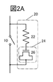
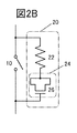
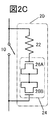
- 2A to 2D are circuit diagrams illustrating one aspect of the present invention.
- 3A and 3B are circuit diagrams illustrating an aspect of the present invention.
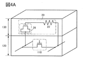
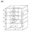
- 4A and 4B are schematic views illustrating an aspect of the present invention.
- FIG. 5 is a schematic view illustrating one aspect of the present invention.
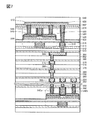
- FIG. 6 is a cross-sectional view showing a configuration example of the semiconductor device according to one aspect of the present invention.
- FIG. 7 is a cross-sectional view showing a configuration example of the semiconductor device according to one aspect of the present invention.
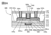
- 8A to 8C are cross-sectional views showing structural examples of transistors.
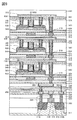
- FIG. 9 is a cross-sectional view showing a configuration example of the semiconductor device according to one aspect of the present invention.
- FIG. 10A is a top view of the semiconductor wafer.
- FIG. 10B is a top view of the chip.
- FIG. 11A is a flowchart illustrating an example of a manufacturing process of electronic components.
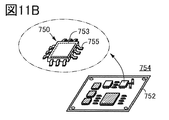
- FIG. 11B is a schematic perspective view of an electronic component.
- FIG. 12 is a diagram showing an example of an electronic device.
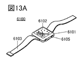
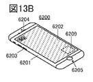
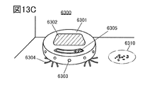
- 13A to 13F are diagrams showing an example of an electronic device.
- FIG. 14 is a diagram showing the hierarchical structure of the IoT network and the tendency of the required specifications.
- FIG. 15 is an image diagram of factory automation.
- FIG. 1 is a diagram showing an example in which a snubber circuit 20 is connected to a switch 10 in a certain circuit.
- the snubber circuit 20 is provided with a resistor 22 and a capacitance 24, and one terminal of the resistor 22 is electrically connected to one electrode of the capacitance 24.
- the other of the terminals of the resistor 22 is electrically connected to one terminal of the switch 10, and the other of the electrodes of the capacitance 24 is electrically connected to the other terminal of the switch 10.
- the snubber circuit 20 absorbs ringing noise or spike voltage generated by the inductance (including not only self-inductance but also parasitic inductance and stray inductance) of the circuit.
- a MOS capacitor using a metal oxide for the semiconductor layer is used as the capacity 24 of the snubber circuit 20 shown in FIG.
- the metal oxide preferably functions as an oxide semiconductor (OS), and in the present specification, a MOS capacitor using a metal oxide in the semiconductor layer is referred to as an OS-MOS capacitor.
- OS-MOS capacitor 26 is provided as the capacity 24 of the snubber circuit 20.
- OS-MOS capacitor 26 a field effect transistor (referred to as OS-FET) using an OS in the semiconductor layer can be used.
- the gate of the OS-FET is used as the first electrode of the OS-MOS capacitor, and the source and drain electrically connected to each other are used as the second electrode.
- FIG. 2A shows an example in which the first electrode is electrically connected to the resistor 22 and the second electrode is electrically connected to the switch 10.
- FIG. 2B shows an example in which the first electrode is electrically connected to the switch 10 and the second electrode is electrically connected to the resistor 22.
- FIG. 2C shows an example in which two OS-MOS capacitors 26A and 26B are used as the capacitance 24.
- the first electrode of the OS-MOS capacitor 26A is electrically connected to the resistor 22, the second electrode of the OS-MOS capacitor 26A and the second electrode of the OS-MOS capacitor 26B are electrically connected, and the OS- The first electrode of the MOS capacitor 26B is electrically connected to the switch 10.
- the number of OS-MOS capacitors 26 provided in the snubber circuit 20 is not particularly limited, and a plurality of OS-MOS capacitors 26 may be provided depending on the capacitance value required by the snubber circuit 20 or the circuit in which the snubber circuit 20 is provided.
- FIG. 2D shows an example in which a plurality of OS-MOS capacitors 26 are connected in parallel as the capacitance 24.
- the configuration of the OS-MOS capacitor is not limited to this.
- the OS-MOS capacitors having the configuration shown in FIG. 2B or FIG. 2C can be connected in parallel.
- a plurality of OS-MOS capacitors are provided as the capacitance 24, a plurality of OS-FETs are prepared, and the gates of the plurality of OS-FETs are electrically connected to form the first electrode of the capacitance 24, and the respective sources and drains are electrically connected. It can be used as a second electrode having a capacity of 24 by connecting the electrodes.
- FIG. 2D shows an example in which the first electrode of the capacitance 24 is electrically connected to the resistor 22 and the second electrode is electrically connected to the switch 10, but the present embodiment is not limited to this.
- the first electrode of the capacitance 24 may be electrically connected to the switch 10 and the second electrode may be electrically connected to the resistor 22.
- the converter circuit 111 shown in FIG. 3A is a DCDC converter circuit (synchronous rectification type buck converter circuit) having a transistor 112, a coil 113, a transistor 118, a capacitor 115, and a resistor 116.
- DCDC converter circuit synchronous rectification type buck converter circuit
- One of the source and drain of the transistor 112 is electrically connected to one electrode of the power supply 117.
- the other of the source and drain of the transistor 112 is electrically connected to one of the source and drain of the transistor 118 and one of the terminals of the coil 113.
- the other of the source and drain of the transistor 118 is electrically connected to the other electrode of the power supply 117, one terminal of the capacitor 115, and one terminal of the resistor 116.
- the other terminal of the coil 113 is electrically connected to the other terminal of the capacitor 115, the other terminal of the resistor 116, and the output terminal OUT.
- the other electrode of the power supply 117, the source and drain of the transistor 118, one terminal of the capacitor 115, and one terminal of the resistor 116 are electrically connected to the terminal GND and grounded.
- the transistor 112 functions as a switching element.
- the gate of the transistor 112 is connected to the control circuit of the converter circuit 111.
- the transistor 112 is turned on or off by the signal from the control circuit of the converter circuit 111.
- the potential of one electrode of the power supply 117 is V1
- the potential of the output terminal OUT is V2.
- the transistor 112 which is a switching element, is in the ON state, V2 and V1 are equipotential. At this time, exciting energy is stored in the coil 113 due to the current of the buck converter circuit flowing from the input to the output.
- the transistor 118 When the transistor 112 is turned off, the transistor 118 is turned on in synchronization with the turning off of the transistor 112.
- the voltage V2 drops as the current flows through the transistor 118. Since the voltage V2 is lower than the voltage V1, the converter circuit 111 functions as a step-down converter circuit.
- Ringing noise or spike voltage may occur in the converter circuit 111 due to the switching operation of the transistor 112 and the transistor 118.
- the influence of ringing noise and spike voltage may be noticeable.
- a snubber circuit 20 is provided in the converter circuit 111 in order to suppress these effects.
- one terminal of the snubber circuit 20 is electrically connected to the source and drain of the transistor 112, the source and drain of the transistor 118, and one terminal of the coil 113. Further, the other terminal of the snubber circuit 20 is electrically connected to the other of the source and drain of the transistor 118, the other electrode of the power supply 117, one terminal of the capacitor 115, and one terminal of the resistor 116.
- the configurations shown in FIGS. 2A to 2D can be used. Further, the resistor 22 side is used as one terminal of the snubber circuit 20, and the capacitance 24 side is used as the other terminal of the snubber circuit 20, but the present embodiment is not limited to this.
- the capacitance 24 side is electrically connected to one of the source and drain of the transistor 118 as one terminal of the snubber circuit 20, and the resistor 22 side is connected to the other of the source and drain of the transistor 118 as the other terminal of the snubber circuit 20. It may be connected electrically.
- the layer on which the transistor 112 and the transistor 118 are provided and the layer on which the OS-MOS capacitor 26 is provided are different from each other. By doing so, it is possible to suppress an increase in the area of a circuit such as the converter circuit 111 due to the OS-MOS capacitor 26.
- a transistor 112 and a transistor 118 are provided on the semiconductor substrate so that a part of the semiconductor substrate becomes a channel forming region of the transistor 112 and the transistor 118, and an OS-MOS capacitor 26 is provided above the transistor 112 and the transistor 118. It is preferable to provide.
- the material contained in the semiconductor substrate Si, Ge, SiGe, GaAs, GaAlAs, GaN, InP and the like can be used.
- the transistor 112 and the transistor 118 may be provided on the insulating surface, and the OS-MOS capacitor 26 may be provided above the transistor 112 and the transistor 118.
- CVD chemical vapor deposition
- MBE molecular beam epitaxy
- PLD Pulsed Laser Deposition
- Method or the like may be used to form a semiconductor layer to form a channel forming region of the transistor 112 and the transistor 118.
- a semiconductor layer may be laminated on the insulating surface to form a channel forming region for the transistor 112 and the transistor 118.
- Si, GaAs, GaN, InP, or the like can be used as the material contained in the semiconductor layer.
- a metal oxide that can be used for the OS-MOS capacitor 26 can be used as the material contained in the semiconductor layer.
- the same material as the metal oxide used for the OS-MOS capacitor 26 may be used for the transistor 112 and the transistor 118, or different metal oxides may be used.
- an asynchronous rectifying type step-down converter can be used by replacing the transistor 118 of the converter circuit 111 with a diode 119.
- the converter circuit 111A shown in FIG. 3B is a DCDC converter circuit (asynchronous rectification type buck converter circuit) having a transistor 112, a coil 113, a diode 119, a capacitor 115, and a resistor 116.
- a diode 119 a diode-connected transistor 118 or the like can be used.
- One of the source and drain of the transistor 112 is electrically connected to one electrode of the power supply 117.
- the other of the source or drain of the transistor 112 is electrically connected to the output terminal of the diode 119 and one terminal of the coil 113.
- the input terminal of the diode 119 is electrically connected to the other electrode of the power supply 117, one terminal of the capacitor 115, and one terminal of the resistor 116.
- the other terminal of the coil 113 is electrically connected to the other terminal of the capacitor 115, the other terminal of the resistor 116, and the output terminal OUT.
- the other electrode of the power supply 117, the input terminal of the diode 119, one terminal of the capacitor 115, and one terminal of the resistor 116 are electrically connected to the terminal GND and grounded.
- the transistor 112 functions as a switching element.
- the gate of the transistor 112 is connected to the control circuit of the converter circuit 111A.
- the transistor 112 is turned on or off by the signal from the control circuit of the converter circuit 111A.
- the potential of one electrode of the power supply 117 is V1
- the potential of the output terminal OUT is V2.
- the transistor 112 which is a switching element, is in the ON state, V2 and V1 are equipotential. At this time, exciting energy is stored in the coil 113 due to the current of the buck converter circuit flowing from the input to the output.
- the coil 113 When the transistor 112 is turned off, the coil 113 generates an electromotive force to maintain the current and turns the diode 119 into the on state.
- the voltage V2 drops as the current flows through the diode 119. Since the voltage V2 is lower than the voltage V1, the converter circuit 111A functions as a step-down converter circuit.
- Ringing noise or spike voltage may occur in the converter circuit 111A due to the switching operation of the transistor 112.
- the influence of ringing noise and spike voltage may be noticeable.
- a snubber circuit 20 is provided in the converter circuit 111A.
- one terminal of the snubber circuit 20 is electrically connected to the source or drain of the transistor 112, the output terminal of the diode 119, and one terminal of the coil 113.
- the other terminal of the snubber circuit 20 is electrically connected to the input terminal of the diode 119, the other electrode of the power supply 117, one terminal of the capacitor 115, and one terminal of the resistor 116.
- the configurations shown in FIGS. 2A to 2D can be used. Further, the resistor 22 side is used as one terminal of the snubber circuit 20, and the capacitance 24 side is used as the other terminal of the snubber circuit 20, but the present embodiment is not limited to this.
- the capacity 24 side is electrically connected to the output terminal of the diode 119 as one terminal of the snubber circuit 20, and the resistor 22 side is electrically connected to the input terminal of the diode 119 as the other terminal of the snubber circuit 20. May be good.
- the layer on which the transistor 112 and the diode 119 are provided and the layer on which the OS-MOS capacitor 26 is provided are different from each other. By doing so, it is possible to suppress an increase in the area of a circuit such as the converter circuit 111A due to the OS-MOS capacitor 26.
- a transistor 112 and a diode 119 are provided on the semiconductor substrate so that a part of the semiconductor substrate becomes a channel forming region of the transistor 112 and a diode 119, and an OS-MOS capacitor 26 is provided above the transistor 112 and the diode 119. It is preferable to provide.
- the material contained in the semiconductor substrate Si, Ge, SiGe, GaAs, GaAlAs, GaN, InP and the like can be used.
- the transistor 112 and the diode 119 may be provided on the insulating surface, and the OS-MOS capacitor 26 may be provided above the transistor 112 and the diode 119.
- a semiconductor layer may be formed on the insulating surface by using a sputtering method, a CVD method, an MBE method, a PLD method, an ALD method, or the like to form a channel forming region for the transistor 112 and the diode 119.
- a semiconductor layer may be laminated on the insulating surface to form a channel forming region for the transistor 112 and the diode 119.
- Si, GaAs, GaN, InP, or the like can be used as the material contained in the semiconductor layer.
- a metal oxide that can be used for the OS-MOS capacitor 26 can be used as the material contained in the semiconductor layer.
- the same material as the metal oxide used for the OS-MOS capacitor 26 may be used for the transistor 112 and the diode 119, or different metal oxides may be used.
- an oxide containing at least one of indium (In), gallium (Ga), and zinc (Zn) can be used.
- In-M-Zn oxide element M is aluminum, gallium, yttrium, tin, copper, vanadium, beryllium, boron, titanium, iron, nickel, germanium, zirconium, molybdenum, lantern, cerium).
- Neodymium, hafnium, tantalum, tungsten, magnesium, etc. (one or more) and the like may be used.
- aluminum, gallium, yttrium, tin and the like are preferably contained.
- the metal oxide preferably has a crystal structure.
- the metal oxide having a crystal structure include CAAC-OS (c-axis aligned crystalline oxide semiconductor), polycrystalline oxide semiconductor, and nc-OS (nanocrystalline oxide semiconductor).
- CAAC-OS has a c-axis orientation and has a distorted crystal structure in which a plurality of nanocrystals are connected in the ab plane direction.
- the strain refers to a region in which a plurality of nanocrystals are connected, in which the orientation of the lattice arrangement changes between a region in which the lattice arrangement is aligned and a region in which another lattice arrangement is aligned.
- nanocrystals are basically hexagonal, they are not limited to regular hexagons and may have non-regular hexagons. In addition, it may have a lattice arrangement such as a pentagon and a heptagon in distortion.
- CAAC-OS it is difficult to confirm a clear grain boundary (also referred to as grain boundary) even in the vicinity of strain. That is, it can be seen that the formation of grain boundaries is suppressed by the distortion of the lattice arrangement. This is because CAAC-OS can tolerate distortion because the arrangement of oxygen atoms is not dense in the ab plane direction and the bond distance between atoms changes due to substitution of metal elements. Because.
- CAAC-OS is a layered crystal in which a layer having indium and oxygen (hereinafter, In layer) and a layer having elements M, zinc, and oxygen (hereinafter, (M, Zn) layer) are laminated. It tends to have a structure (also called a layered structure). Indium and the element M can be replaced with each other, and when the element M of the (M, Zn) layer is replaced with indium, it can be expressed as the (In, M, Zn) layer. Further, when the indium of the In layer is replaced with the element M, it can be expressed as the (In, M) layer.
- CAAC-OS is a highly crystalline metal oxide.
- CAAC-OS it is difficult to confirm a clear grain boundary, so it can be said that a decrease in electron mobility due to the crystal grain boundary is unlikely to occur.
- CAAC-OS impurities and defects oxygen deficiency (V O:. Oxygen vacancy also referred) etc.) with less metal It can also be called an oxide. Therefore, the metal oxide having CAAC-OS has stable physical properties. Therefore, the metal oxide having CAAC-OS is resistant to heat and has high reliability.
- the nc-OS has periodicity in the atomic arrangement in a minute region (for example, a region of 1 nm or more and 10 nm or less, particularly a region of 1 nm or more and 3 nm or less).
- nc-OS does not show regularity in crystal orientation between different nanocrystals. Therefore, no orientation is observed in the entire film. Therefore, nc-OS may be indistinguishable from a-like OS and amorphous oxide semiconductors depending on the analysis method.
- Indium-gallium-zinc oxide which is a kind of metal oxide having indium, gallium, and zinc, may have a stable structure by forming the above-mentioned nanocrystals. is there.
- IGZO tends to have difficulty in crystal growth in the atmosphere, it is preferable to use smaller crystals (for example, the above-mentioned nanocrystals) than large crystals (here, a few mm crystal or a few cm crystal). However, it may be structurally stable.
- the metal oxide may be a pseudo-amorphous oxide semiconductor (a-like OS: amorphous-like oxide semiconductor) or an amorphous oxide semiconductor.
- the a-like OS is a metal oxide having a structure between the nc-OS and an amorphous oxide semiconductor.
- the a-like OS has a void or low density region. That is, the a-like OS has lower crystallinity than the nc-OS and CAAC-OS.
- Metal oxides have various structures and each has different properties.
- the metal oxide of one aspect of the present invention may have two or more of an amorphous oxide semiconductor, a polycrystalline oxide semiconductor, a-like OS, nc-OS, and CAAC-OS.
- ⁇ OS-MOS capacitor laminated structure> 4A and 4B show an example in which the snubber circuit 20 or the OS-MOS capacitor 26 included in the snubber circuit 20 is provided above the converter circuit 111.
- the converter circuit 111 is provided in the first circuit layer 120.
- the transistor 118 is shown in the first circuit layer 120 in order to facilitate the understanding of the figure, but the present embodiment is not limited to this.
- the first circuit layer 120 is provided with all or at least a part of the circuit elements constituting the converter circuit 111. Further, the first circuit layer 120 may be provided with all or at least a part of the circuit elements constituting the converter circuit 111A, such as the diode 119.
- a second circuit layer 130 is provided above the first circuit layer 120.
- a snubber circuit 20 having an OS-MOS capacitor 26 is provided in the second circuit layer 130.
- the second circuit layer 130 may be provided with a part of the circuit elements constituting the converter circuit 111.
- the resistor 22 included in the snubber circuit 20 is provided in the second circuit layer 130 is shown, the present embodiment is not limited to this.
- the resistor 22 may be provided in the first circuit layer 120, or may be provided in both the first circuit layer 120 and the second circuit layer 130.
- a plurality of OS-MOS capacitors 26 may be provided in the second circuit layer 130 as shown in FIG. 4B to form the snubber circuit 20.
- a plurality of circuit layers 130_1 to 130_n may be provided on the first circuit layer 120.
- the circuit layer 130_1 can be referred to as a second circuit layer 130_1
- the circuit layer 130_2 can be referred to as a third circuit layer 130_2
- the circuit layer 130_n can be referred to as a (n + 1) th circuit layer 130_n.
- the circuit layers 130_1 to 130_n each have one or more OS-MOS capacitors 26.
- the resistor 22 included in the snubber circuit 20 is provided in the second circuit layer 130_1 is shown, but the present embodiment is not limited to this.
- the resistor 22 may be provided in the first circuit layer 120 or may be provided in the (n + 1) th circuit layer 130_n. Further, it may be provided in one or more of a plurality of circuit layers 120, circuit layers 130_1 to circuit layers 130_n.
- ⁇ Semiconductor device> the transistor configuration applicable to the semiconductor device configuration described above and the transistor configuration applicable to the OS-MOS capacitor will be described. Specifically, a configuration in which transistors having different electrical characteristics are laminated and provided will be described. In particular, in the present embodiment, the configurations of the DCDC converter circuit constituting the semiconductor device and the transistors of the snubber circuit will be described. With this configuration, the degree of freedom in designing the semiconductor device can be increased. Further, by stacking transistors having different electrical characteristics, the degree of integration of the semiconductor device can be increased.
- the semiconductor device shown in FIG. 6 includes a transistor 300 and a transistor 500 that forms an OS-MOS capacitor.
- 8A is a cross-sectional view of the transistor 500 in the channel length direction
- FIG. 8B is a cross-sectional view of the transistor 500 in the channel width direction
- FIG. 8C is a cross-sectional view of the transistor 300 in the channel width direction.
- the transistor 500 is a transistor (OS transistor) having a metal oxide in the channel forming region.
- the semiconductor device described in this embodiment has a transistor 300 and a transistor 500 as shown in FIG.
- the transistor 500 is provided above the transistor 300.
- the source and drain of the transistor 500 are electrically connected by a conductor 612 to form an OS-MOS capacitor.
- the transistor 300 is provided on the substrate 311 and has a semiconductor region 313 composed of a conductor 316, an insulator 315, and a part of the substrate 311, a low resistance region 314a functioning as a source region or a drain region, and a low resistance region 314b. ..
- the transistor 300 can be applied to, for example, the transistor 112, the transistor 118, the diode 119, etc. of the converter circuit 111.
- the transistor 300 has a top surface of the semiconductor region 313 and a side surface in the channel width direction covered with a conductor 316 via an insulator 315.
- the transistor 300 By making the transistor 300 a Fin type in this way, the effective channel width is increased, so that the on-characteristics of the transistor 300 can be improved. Further, since the contribution of the electric field of the gate electrode can be increased, the off characteristic of the transistor 300 can be improved.
- the transistor 300 may be either a p-channel type or an n-channel type.
- a semiconductor such as a silicon-based semiconductor in a region in which a channel of the semiconductor region 313 is formed, a region in the vicinity thereof, a low resistance region 314a serving as a source region or a drain region, a low resistance region 314b, and the like.
- It preferably contains crystalline silicon.
- it may be formed of a material having Ge, SiGe, GaAs, GaAlAs, GaN, InP, or the like.
- a configuration using silicon in which the effective mass is controlled by applying stress to the crystal lattice and changing the lattice spacing may be used.
- the transistor 300 may be a HEMT (High Electron Mobility Transistor) by using GaAs, GaAlAs, GaN, or the like.
- an element that imparts n-type conductivity such as arsenic and phosphorus, or a p-type conductivity such as boron is imparted.
- the conductor 316 that functions as a gate electrode is a semiconductor material such as silicon, a metal material, or an alloy that contains an element that imparts n-type conductivity such as arsenic or phosphorus, or an element that imparts p-type conductivity such as boron.
- a material or a conductive material such as a metal oxide material can be used.
- the threshold voltage of the transistor can be adjusted by selecting the material of the conductor. Specifically, it is preferable to use a material such as titanium nitride or tantalum nitride for the conductor. Further, in order to achieve both conductivity and embedding property, it is preferable to use a metal material such as tungsten or aluminum as a laminate for the conductor, and it is particularly preferable to use tungsten in terms of heat resistance.
- the transistor 300 shown in FIG. 6 is an example, and the transistor 300 is not limited to its structure, and an appropriate transistor may be used according to the circuit configuration and the driving method.
- the semiconductor device is a unipolar circuit containing only OS transistors (meaning transistors having the same polarity as n-channel transistors only, etc.)
- the transistor 300 is configured by using an oxide semiconductor.
- the configuration may be the same as that of the transistor 500. The details of the transistor 500 will be described later.
- An insulator 320, an insulator 322, an insulator 324, and an insulator 326 are laminated in this order so as to cover the transistor 300.
- the insulator 320, the insulator 322, the insulator 324, and the insulator 326 for example, silicon oxide, silicon oxide nitride, silicon nitride oxide, silicon nitride, aluminum oxide, aluminum oxide nitride, aluminum nitride, aluminum nitride and the like can be used. Just do it.
- silicon oxide refers to a material whose composition has a higher oxygen content than nitrogen
- silicon nitride refers to a material whose composition has a higher nitrogen content than oxygen. Is shown.
- aluminum nitride refers to a material whose composition has a higher oxygen content than nitrogen
- aluminum nitride refers to a material whose composition has a higher nitrogen content than oxygen. Is shown.
- the insulator 322 may have a function as a flattening film for flattening a step generated by a transistor 300 or the like provided below the insulator 322.
- the upper surface of the insulator 322 may be flattened by a flattening treatment using a chemical mechanical polishing (CMP) method or the like in order to improve the flatness.
- CMP chemical mechanical polishing
- the insulator 324 it is preferable to use a film having a barrier property so that hydrogen and impurities do not diffuse in the region where the transistor 500 is provided from the substrate 311 or the transistor 300.
- a film having a barrier property against hydrogen for example, silicon nitride formed by a sputtering method can be used. Further, silicon nitride may be formed by using a CVD method or the like.
- hydrogen may diffuse into a semiconductor element having an oxide semiconductor such as a transistor 500, so that the characteristics of the semiconductor element may deteriorate. Therefore, it is preferable to use a film that suppresses the diffusion of hydrogen between the transistor 500 and the transistor 300.
- the membrane that suppresses the diffusion of hydrogen is a membrane that desorbs a small amount of hydrogen.
- the amount of hydrogen desorbed can be analyzed using, for example, a heated desorption gas analysis method (TDS).
- TDS heated desorption gas analysis method
- the amount of hydrogen desorbed from the insulator 324 is the amount desorbed in terms of hydrogen atoms when the surface temperature of the film is in the range of 50 ° C. to 500 ° C. It may be 10 ⁇ 10 15 atoms / cm 2 or less, preferably 5 ⁇ 10 15 atoms / cm 2 or less.
- the insulator 326 has a lower dielectric constant than the insulator 324.
- the relative permittivity of the insulator 326 is preferably less than 4, more preferably less than 3.
- the relative permittivity of the insulator 326 is preferably 0.7 times or less, more preferably 0.6 times or less, the relative permittivity of the insulator 324.
- the insulator 320, the insulator 322, the insulator 324, and the insulator 326 are embedded with a conductor 328 connected to the transistor 300, a conductor 330, and the like.
- the conductor 328 and the conductor 330 have a function as a plug or wiring.
- a conductor having a function as a plug or wiring may collectively give a plurality of structures the same reference numerals.
- the wiring and the plug connected to the wiring may be integrated. That is, a part of the conductor may function as a wiring, and a part of the conductor may function as a plug.
- each plug and wiring As the material of each plug and wiring (conductor 328, conductor 330, etc.), a conductive material such as a metal material, an alloy material, a metal nitride material, or a metal oxide material is used as a single layer or laminated. be able to. It is preferable to use a refractory material such as tungsten or molybdenum that has both heat resistance and conductivity, and it is preferable to use tungsten. Alternatively, it is preferably formed of a low resistance conductive material such as aluminum or copper. Wiring resistance can be reduced by using a low resistance conductive material.
- a wiring layer may be provided on the insulator 326 and the conductor 330.
- the insulator 350, the insulator 352, and the insulator 354 are laminated in this order.
- a conductor 356 is formed on the insulator 350, the insulator 352, and the insulator 354.
- the conductor 356 has a function as a plug or wiring for connecting to the transistor 300.
- the conductor 356 can be provided by using the same material as the conductor 328 and the conductor 330.
- the insulator 350 it is preferable to use an insulator having a barrier property against hydrogen, like the insulator 324.
- the conductor 356 preferably contains a conductor having a barrier property against hydrogen.
- a conductor having a barrier property against hydrogen is formed in the opening of the insulator 350 having a barrier property against hydrogen.
- the conductor having a barrier property against hydrogen for example, tantalum nitride or the like may be used. Further, by laminating tantalum nitride and tungsten having high conductivity, it is possible to suppress the diffusion of hydrogen from the transistor 300 while maintaining the conductivity as wiring. In this case, it is preferable that the tantalum nitride layer having a barrier property against hydrogen has a structure in contact with the insulator 350 having a barrier property against hydrogen.
- a wiring layer may be provided on the insulator 354 and the conductor 356.
- the insulator 360, the insulator 362, and the insulator 364 are laminated in this order.
- a conductor 366 is formed on the insulator 360, the insulator 362, and the insulator 364.
- the conductor 366 has a function as a plug or wiring.
- the conductor 366 can be provided by using the same material as the conductor 328 and the conductor 330.
- the insulator 360 it is preferable to use an insulator having a barrier property against hydrogen, like the insulator 324.
- the conductor 366 preferably contains a conductor having a barrier property against hydrogen.
- a conductor having a barrier property against hydrogen is formed in the opening of the insulator 360 having a barrier property against hydrogen.
- a wiring layer may be provided on the insulator 364 and the conductor 366.
- the insulator 370, the insulator 372, and the insulator 374 are laminated in this order.
- a conductor 376 is formed on the insulator 370, the insulator 372, and the insulator 374.
- the conductor 376 has a function as a plug or wiring.
- the conductor 376 can be provided by using the same material as the conductor 328 and the conductor 330.
- the insulator 370 it is preferable to use an insulator having a barrier property against hydrogen, similarly to the insulator 324.
- the conductor 376 preferably contains a conductor having a barrier property against hydrogen.
- a conductor having a barrier property against hydrogen is formed in the opening of the insulator 370 having a barrier property against hydrogen.
- a wiring layer may be provided on the insulator 374 and the conductor 376.
- the insulator 380, the insulator 382, and the insulator 384 are laminated in this order.
- a conductor 386 is formed on the insulator 380, the insulator 382, and the insulator 384.
- the conductor 386 has a function as a plug or wiring.
- the conductor 386 can be provided by using the same material as the conductor 328 and the conductor 330.
- the insulator 380 it is preferable to use an insulator having a barrier property against hydrogen, like the insulator 324.
- the conductor 386 preferably contains a conductor having a barrier property against hydrogen.
- a conductor having a barrier property against hydrogen is formed in the opening of the insulator 380 having a barrier property against hydrogen.
- the semiconductor device according to the present embodiment has been described. It is not limited to this.
- the number of wiring layers similar to the wiring layer containing the conductor 356 may be three or less, or the number of wiring layers similar to the wiring layer including the conductor 356 may be five or more.
- Insulator 510, insulator 512, insulator 514, and insulator 516 are laminated in this order on the insulator 384 and the conductor 386.
- any of the insulator 510, the insulator 512, the insulator 514, and the insulator 516 it is preferable to use a substance having a barrier property against oxygen and hydrogen.
- a film having a barrier property so that hydrogen and impurities do not diffuse from the area where the substrate 311 or the transistor 300 is provided to the area where the transistor 500 is provided is used. Is preferable. Therefore, the same material as the insulator 324 can be used.
- Silicon nitride formed by the sputtering method can be used as an example of a film having a barrier property against hydrogen. Further, silicon nitride may be formed by using a CVD method or the like.
- hydrogen may diffuse into a semiconductor element having an oxide semiconductor such as a transistor 500, so that the characteristics of the semiconductor element may deteriorate. Therefore, it is preferable to use a film that suppresses the diffusion of hydrogen between the transistor 500 and the transistor 300.
- the membrane that suppresses the diffusion of hydrogen is a membrane that desorbs a small amount of hydrogen.
- metal oxides such as aluminum oxide, hafnium oxide, and tantalum oxide for the insulator 510 and the insulator 514.
- aluminum oxide has a high blocking effect that does not allow the membrane to permeate both oxygen and impurities such as hydrogen and water, which are factors that change the electrical characteristics of transistors. Therefore, aluminum oxide can prevent impurities such as hydrogen and water from being mixed into the transistor 500 during and after the manufacturing process of the transistor. In addition, the release of oxygen from the oxides constituting the transistor 500 can be suppressed. Therefore, it is suitable for use as a protective film for the transistor 500.
- the same material as the insulator 320 can be used for the insulator 512 and the insulator 516. Further, by applying a material having a relatively low dielectric constant to these insulators, it is possible to reduce the parasitic capacitance generated between the wirings.
- a silicon oxide film, a silicon nitride film, or the like can be used as the insulator 512 and the insulator 516.
- a conductor 518 a conductor constituting the transistor 500 (for example, a conductor 503) and the like are embedded.
- the conductor 518 has a function as a plug or wiring for connecting to the transistor 300.
- the conductor 518 can be provided by using the same material as the conductor 328 and the conductor 330.
- the conductor 510 and the conductor 518 in the region in contact with the insulator 514 are preferably conductors having a barrier property against oxygen, hydrogen, and water.
- the transistor 300 and the transistor 500 can be separated by a layer having a barrier property against oxygen, hydrogen, and water, and the diffusion of hydrogen from the transistor 300 to the transistor 500 can be suppressed.
- a transistor 500 is provided above the insulator 516.
- the conductor 500 includes a conductor 503 arranged so as to be embedded in the insulator 514 and the insulator 516, and an insulator 522 arranged on the insulator 516 and the conductor 503. And an insulator 524 arranged on the insulator 522, an oxide 530a arranged on the insulator 524, an oxide 530b arranged on the oxide 530a, and each other on the oxide 530b.
- 530ca and 530cc of oxides arranged apart from each other, 542aa of conductors arranged on 530ca of oxides, 542b of conductors arranged on 530cc of oxides, and 542a and 542b of conductors.
- the insulator 580 is arranged on the conductor 542a and the conductor 542b to form an opening, the oxide 530d is arranged on the bottom surface and the side surface of the opening, and the oxide 530d is formed. It has an insulator 550 and a conductor 560 arranged on the forming surface of the insulator 550.
- an insulator 544 is arranged between the oxide 530a, the oxide 530b, the oxide 530ca, the oxide 530cc, the conductor 542a, and the conductor 542b and the insulator 580. It is preferable to be done.
- the conductor 560 includes a conductor 560a provided inside the insulator 550 and a conductor 560b provided so as to be embedded inside the conductor 560a. It is preferable to have.
- the insulator 574 is arranged on the insulator 580, the conductor 560, and the insulator 550.
- oxide 530a, oxide 530b, oxide 530ca, oxide 530cc, and oxide 530d may be collectively referred to as oxide 530.
- the transistor 500 shows a configuration in which three layers of oxide 530a, oxide 530b, and oxide 530d are laminated in a region where a channel is formed and in the vicinity thereof, but the present invention is limited to this. It's not a thing.
- FIG. 6 shows an example in which the oxide 530d is not provided in the transistor 500.
- the transistor 300 is not provided with the oxide 530d and the transistor 500 is provided with the oxide 530d. In this way, transistors having different characteristics can be provided in one semiconductor device.
- the transistor 300 may have the same configuration as the transistor 500, and any transistor may be provided with the oxide 530d, or none of the transistors may be provided with the oxide 530d.
- the conductor 560 is shown as a two-layer laminated structure, but the present invention is not limited to this.
- the conductor 560 may have a single-layer structure or a laminated structure of three or more layers.
- the transistor 500 shown in FIGS. 6 and 8A is an example, and the transistor 500 is not limited to the structure thereof, and an appropriate transistor may be used according to the circuit configuration and the driving method.
- the conductor 560 functions as a gate electrode of the transistor, and the conductor 542a and the conductor 542b function as a source electrode or a drain electrode, respectively.
- the conductor 560 is formed so as to be embedded in the opening of the insulator 580 and the region sandwiched between the conductor 542a and the conductor 542b.
- the arrangement of the conductor 560, the conductor 542a and the conductor 542b is self-aligned with respect to the opening of the insulator 580. That is, in the transistor 500, the gate electrode can be arranged in a self-aligned manner between the source electrode and the drain electrode. Therefore, since the conductor 560 can be formed without providing the alignment margin, the occupied area of the transistor 500 can be reduced. As a result, the semiconductor device can be miniaturized and highly integrated.
- the conductor 560 is formed in a region between the conductor 542a and the conductor 542b in a self-aligned manner, the conductor 560 does not have a region that overlaps with the conductor 542a or the conductor 542b. Thereby, the parasitic capacitance formed between the conductor 560 and the conductors 542a and 542b can be reduced. Therefore, the switching speed of the transistor 500 can be improved and a high frequency characteristic can be provided.
- the conductor 560 may function as a first gate (also referred to as a top gate) electrode. Further, the conductor 503 may function as a second gate (also referred to as a bottom gate) electrode.
- the threshold voltage of the transistor 500 can be controlled by changing the potential applied to the conductor 503 independently of the potential applied to the conductor 560 without interlocking with it. In particular, by applying a negative potential to the conductor 503, the threshold voltage of the transistor 500 can be made larger than 0 V, and the off-current can be reduced. Therefore, when a negative potential is applied to the conductor 503, the drain current when the potential applied to the conductor 560 is 0 V can be made smaller than when it is not applied.
- the conductor 503 is arranged so as to overlap the oxide 530 and the conductor 560. As a result, when a potential is applied to the conductor 560 and the conductor 503, the electric field generated from the conductor 560 and the electric field generated from the conductor 503 are connected to cover the channel forming region formed in the oxide 530. Can be done.
- the structure of the transistor that electrically surrounds the channel formation region by the electric fields of the first gate electrode and the second gate electrode is referred to as a surroundd channel (S-channel) structure.
- the conductor 503 has the same configuration as the conductor 518, and the conductor 503a is formed in contact with the inner wall of the opening of the insulator 514 and the insulator 516, and the conductor 503b is further formed inside.
- the transistor 500 shows a configuration in which the conductor 503a and the conductor 503b are laminated, but the present invention is not limited to this.
- the conductor 503 may be provided as a single layer or a laminated structure having three or more layers.
- a conductive material for the conductor 503a which has a function of suppressing the diffusion of impurities such as hydrogen atoms, hydrogen molecules, water molecules, and copper atoms (the above impurities are difficult to permeate).
- a conductive material having a function of suppressing the diffusion of oxygen for example, at least one oxygen atom, oxygen molecule, etc.
- the function of suppressing the diffusion of impurities or oxygen is a function of suppressing the diffusion of any one or all of the above impurities or the above oxygen.
- the conductor 503a since the conductor 503a has a function of suppressing the diffusion of oxygen, it is possible to prevent the conductor 503b from being oxidized and the conductivity from being lowered.
- the conductor 503 also functions as a wiring, it is preferable to use a highly conductive conductive material containing tungsten, copper, or aluminum as a main component for the conductor 503b.
- the conductor 503b is shown as a single layer, it may have a laminated structure, for example, titanium or titanium nitride may be laminated with the conductive material.
- the insulator 522 and the insulator 524 have a function as a second gate insulating film.
- the insulator 524 in contact with the oxide 530 it is preferable to use an insulator containing more oxygen than oxygen satisfying the stoichiometric composition. That is, it is preferable that the insulator 524 is formed with an excess oxygen region. By providing such an insulator containing excess oxygen in contact with the oxide 530, oxygen deficiency in the oxide 530 can be reduced and the reliability of the transistor 500 can be improved.
- the insulator having an excess oxygen region it is preferable to use an oxide material in which a part of oxygen is desorbed by heating.
- Oxides that desorb oxygen by heating are those in which the amount of oxygen desorbed in terms of oxygen atoms is 1.0 ⁇ 10 18 atoms / cm 3 or more, preferably 1 in TDS (Thermal Desolation Spectroscopy) analysis.
- the surface temperature of the film during the TDS analysis is preferably in the range of 100 ° C. or higher and 700 ° C. or lower, or 100 ° C. or higher and 400 ° C. or lower.
- the insulator 524 has an excess oxygen region, it is preferable that the insulator 522 has a function of suppressing the diffusion of oxygen (for example, oxygen atom, oxygen molecule, etc.) (the oxygen is difficult to permeate).
- oxygen for example, oxygen atom, oxygen molecule, etc.
- the insulator 522 has a function of suppressing the diffusion of oxygen and impurities, the oxygen contained in the oxide 530 does not diffuse to the insulator 512 side, which is preferable. Further, it is possible to suppress the conductor 503 from reacting with the oxygen contained in the insulator 524 and the oxide 530.
- the insulator 522 is, for example, aluminum oxide, hafnium oxide, an oxide containing aluminum and hafnium (hafnium aluminate), tantalum oxide, zirconium oxide, lead zircate titanate (PZT), strontium titanate (SrTIO 3 ), or It is preferable to use an insulator containing a so-called high-k material such as (Ba, Sr) TiO 3 (BST) in a single layer or in a laminated state.
- a so-called high-k material such as (Ba, Sr) TiO 3 (BST)
- an insulator containing oxides of one or both of aluminum and hafnium which are insulating materials having a function of suppressing diffusion of impurities and oxygen (the above oxygen is difficult to permeate).
- the insulator containing one or both oxides of aluminum and hafnium it is preferable to use aluminum oxide, hafnium oxide, an oxide containing aluminum and hafnium (hafnium aluminate) and the like.
- the insulator 522 is formed by using such a material, the insulator 522 suppresses the release of oxygen from the oxide 530 and the mixing of impurities such as hydrogen from the peripheral portion of the transistor 500 into the oxide 530. Acts as a layer.
- aluminum oxide, bismuth oxide, germanium oxide, niobium oxide, silicon oxide, titanium oxide, tungsten oxide, yttrium oxide, and zirconium oxide may be added to these insulators.
- these insulators may be nitrided. Silicon oxide, silicon oxide or silicon nitride may be laminated on the above insulator.
- the insulator 516 is thermally stable.
- silicon oxide and silicon oxynitride are suitable because they are thermally stable.
- the insulator 522 and the insulator 524 are shown as the second gate insulating film having a two-layer laminated structure, but the second gate insulating film is It may have a single layer, three layers, or a laminated structure of four or more layers. In that case, the laminated structure is not limited to the same material, and may be a laminated structure made of different materials.
- oxide 530 a metal oxide that functions as an oxide semiconductor for the oxide 530 including the channel forming region.
- oxide 530 In-M-Zn oxide (element M is aluminum, gallium, yttrium, copper, vanadium, beryllium, boron, titanium, iron, nickel, germanium, zirconium, molybdenum, lantern, cerium, neodymium). , Hafnium, tantalum, tungsten, magnesium, etc. (one or more) and the like may be used.
- the In-M-Zn oxide applicable as the oxide 530 is preferably CAAC-OS or CAC-OS described in the fourth embodiment.
- the oxide 530 can suppress the diffusion of impurities from the structure formed below the oxide 530a to the oxide 530b. Further, by having the oxide 530d on the oxide 530b, it is possible to suppress the diffusion of impurities into the oxide 530b from the structure formed above the oxide 530d.
- the oxide 530 has a laminated structure of a plurality of oxide layers having different atomic number ratios of each metal atom.
- the atomic number ratio of the element M in the constituent elements is larger than the atomic number ratio of the element M in the constituent elements in the metal oxide used in the oxide 530b.
- the atomic number ratio of the element M to In is preferably larger than the atomic number ratio of the element M to In in the metal oxide used for the oxide 530b.
- the atomic number ratio of In to the element M is preferably larger than the atomic number ratio of In to the element M in the metal oxide used for the oxide 530a.
- the oxide 530ca and the oxide 530cc a metal oxide that can be used for the oxide 530a can be used.
- the oxide 530d a metal oxide that can be used for the oxide 530a or the oxide 530b can be used.
- the energy at the lower end of the conduction band of the oxide 530a and the oxide 530d is higher than the energy at the lower end of the conduction band of the oxide 530b.
- the electron affinity of the oxide 530a and the oxide 530d is smaller than the electron affinity of the oxide 530b.
- the energy level at the lower end of the conduction band changes gently.
- the energy level at the lower end of the conduction band at the junction of the oxide 530a, the oxide 530b, and the oxide 530d is continuously changed or continuously bonded.
- the oxide 530a and the oxide 530b, and the oxide 530b and the oxide 530d have a common element (main component) other than oxygen, so that a mixed layer having a low defect level density is formed.
- a common element (main component) other than oxygen so that a mixed layer having a low defect level density is formed.
- the oxide 530b is an In-Ga-Zn oxide, In-Ga-Zn oxide, Ga-Zn oxide, gallium oxide or the like may be used as the oxide 530a and the oxide 530d.
- the main path of the carrier is oxide 530b.
- the defect level density at the interface between the oxide 530a and the oxide 530b and the interface between the oxide 530b and the oxide 530d can be lowered. Therefore, the influence of interfacial scattering on carrier conduction is reduced, and the transistor 500 can obtain a high on-current.
- a conductor 542a and a conductor 542b that function as a source electrode and a drain electrode are provided on the oxide 530ca and the oxide 530cc.
- Examples of the conductor 542a and the conductor 542b include aluminum, chromium, copper, silver, gold, platinum, tantalum, nickel, titanium, molybdenum, tungsten, hafnium, vanadium, niobium, manganese, magnesium, zirconium, beryllium, indium, and ruthenium.
- Iridium, strontium, lanthanum, or an alloy containing the above-mentioned metal element as a component, or an alloy in which the above-mentioned metal element is combined is preferably used.
- tantalum nitride, titanium nitride, tungsten, nitrides containing titanium and aluminum, nitrides containing tantalum and aluminum, ruthenium oxide, ruthenium nitride, oxides containing strontium and ruthenium, oxides containing lanthanum and nickel, etc. are used. Is preferable.
- tantalum nitride, titanium nitride, nitrides containing titanium and aluminum, nitrides containing tantalum and aluminum, ruthenium oxide, ruthenium nitride, oxides containing strontium and ruthenium, and oxides containing lanthanum and nickel are difficult to oxidize.
- a metal nitride film such as tantalum nitride is preferable because it has a barrier property against hydrogen or oxygen.
- the conductor 542a and the conductor 542b are shown as a single-layer structure, but a laminated structure of two or more layers may be used.
- a tantalum nitride film and a tungsten film may be laminated.
- the titanium film and the aluminum film may be laminated.
- a two-layer structure in which an aluminum film is laminated on a tungsten film a two-layer structure in which a copper film is laminated on a copper-magnesium-aluminum alloy film, a two-layer structure in which a copper film is laminated on a titanium film, and a tungsten film. It may have a two-layer structure in which copper films are laminated.
- a three-layer structure, a molybdenum film or a molybdenum film or a titanium film or a titanium nitride film is superposed on the titanium film or the titanium nitride film and an aluminum film or a copper film is laminated, and a titanium film or a titanium nitride film is further formed on the aluminum film or the copper film.
- a molybdenum nitride film and an aluminum film or a copper film are laminated on the molybdenum film or the molybdenum nitride film, and a molybdenum film or a molybdenum nitride film is further formed on the aluminum film or the copper film.
- a transparent conductive material containing indium oxide, tin oxide or zinc oxide may be used.
- a region 543a and a region 543b may be formed as low resistance regions at the interface of the oxide 530 with the conductor 542a (conductor 542b) and its vicinity.
- the region 543a functions as one of the source region or the drain region
- the region 543b functions as the other of the source region or the drain region.
- a channel forming region is formed in a region sandwiched between the region 543a and the region 543b.
- the oxygen concentration in the region 543a (region 543b) may be reduced. Further, in the region 543a (region 543b), a metal compound layer containing the metal contained in the conductor 542a (conductor 542b) and the component of the oxide 530 may be formed. In such a case, the carrier density of the region 543a (region 543b) increases, and the region 543a (region 543b) becomes a low resistance region.
- the insulator 544 is provided so as to cover the conductor 542a and the conductor 542b, and suppresses the oxidation of the conductor 542a and the conductor 542b. At this time, the insulator 544 may be provided so as to cover the side surface of the oxide 530 and come into contact with the insulator 524.
- insulator 544 a metal oxide containing one or more selected from hafnium, aluminum, gallium, yttrium, zirconium, tungsten, titanium, tantalum, nickel, germanium, neodymium, lantern, magnesium, etc. Can be used. Further, as the insulator 544, silicon nitride oxide, silicon nitride or the like can also be used.
- the insulator 544 it is preferable to use aluminum or an oxide containing one or both oxides of hafnium, such as aluminum oxide, hafnium oxide, aluminum, and an oxide containing hafnium (hafnium aluminate). ..
- hafnium aluminate has higher heat resistance than the hafnium oxide film. Therefore, it is preferable because it is difficult to crystallize in the heat treatment in the subsequent step.
- the conductors 542a and 542b are made of a material having oxidation resistance, or if the conductivity does not significantly decrease even if oxygen is absorbed, the insulator 544 is not an essential configuration. It may be appropriately designed according to the desired transistor characteristics.
- the insulator 544 By having the insulator 544, it is possible to prevent impurities such as water and hydrogen contained in the insulator 580 from diffusing into the oxide 530b via the oxide 530d and the insulator 550. Further, it is possible to suppress the oxidation of the conductor 560 due to the excess oxygen contained in the insulator 580.
- the insulator 550 functions as a first gate insulating film.
- the insulator 550 is preferably arranged in contact with the inside (upper surface and side surface) of the oxide 530d.
- the insulator 550 is preferably formed by using an insulator that contains excess oxygen and releases oxygen by heating, similarly to the above-mentioned insulator 524.
- silicon oxide having excess oxygen silicon oxide, silicon nitride, silicon nitride, silicon oxide to which fluorine is added, silicon oxide to which carbon is added, carbon, silicon oxide to which nitrogen is added, and vacancies are used.
- Silicon oxide having can be used.
- silicon oxide and silicon nitride nitride are preferable because they are stable against heat.
- oxygen can be effectively applied from the insulator 550 through the oxide 530d to the channel forming region of the oxide 530b. Can be supplied. Further, similarly to the insulator 524, it is preferable that the concentration of impurities such as water or hydrogen in the insulator 550 is reduced.
- the film thickness of the insulator 550 is preferably 1 nm or more and 20 nm or less.
- a metal oxide may be provided between the insulator 550 and the conductor 560.
- the metal oxide preferably suppresses oxygen diffusion from the insulator 550 to the conductor 560.
- the diffusion of excess oxygen from the insulator 550 to the conductor 560 is suppressed. That is, it is possible to suppress a decrease in the amount of excess oxygen supplied to the oxide 530.
- oxidation of the conductor 560 due to excess oxygen can be suppressed.
- a material that can be used for the insulator 544 may be used.
- the insulator 550 may have a laminated structure as in the case of the second gate insulating film.
- an insulator that functions as a gate insulating film is made of a high-k material and heat.
- the conductor 560 that functions as the first gate electrode is shown as a two-layer structure in FIGS. 8A and 8B, but may have a single-layer structure or a laminated structure of three or more layers.
- Conductor 560a is a hydrogen atom, a hydrogen molecule, a water molecule, a nitrogen atom, a nitrogen molecule, nitric oxide molecule (N 2 O, NO, etc. NO 2), conductive having a function of suppressing the diffusion of impurities such as copper atoms It is preferable to use a material. Alternatively, it is preferable to use a conductive material having a function of suppressing the diffusion of oxygen (for example, at least one oxygen atom, oxygen molecule, etc.). Since the conductor 560a has a function of suppressing the diffusion of oxygen, it is possible to prevent the conductor 560b from being oxidized by the oxygen contained in the insulator 550 to reduce the conductivity.
- the conductive material having a function of suppressing the diffusion of oxygen for example, tantalum, tantalum nitride, ruthenium, ruthenium oxide and the like are preferably used.
- an oxide semiconductor applicable to the oxide 530 can be used as the conductor 560a. In that case, by forming the conductor 560b into a film by a sputtering method, the electric resistance value of the conductor 560a can be lowered to form a conductor. This can be called an OC (Oxide Conductor) electrode.
- the conductor 560b it is preferable to use a conductive material containing tungsten, copper, or aluminum as a main component. Further, since the conductor 560b also functions as wiring, it is preferable to use a conductor having high conductivity. For example, a conductive material containing tungsten, copper, or aluminum as a main component can be used. Further, the conductor 560b may have a laminated structure, for example, a laminated structure of titanium or titanium nitride and the conductive material.
- the insulator 580 is provided on the conductor 542a and the conductor 542b via the insulator 544.
- the insulator 580 preferably has an excess oxygen region.
- silicon, resin, or the like silicon oxide and silicon oxide nitride are preferable because they are thermally stable.
- silicon oxide and silicon oxide having pores are preferable because an excess oxygen region can be easily formed in a later step.
- the insulator 580 preferably has an excess oxygen region. By providing the insulator 580 from which oxygen is released by heating in contact with the oxide 530d, the oxygen in the insulator 580 can be efficiently supplied to the oxide 530 through the oxide 530d. It is preferable that the concentration of impurities such as water and hydrogen in the insulator 580 is reduced.
- the opening of the insulator 580 is formed so as to overlap the region between the conductor 542a and the conductor 542b.
- the conductor 560 is formed so as to be embedded in the opening of the insulator 580 and the region sandwiched between the conductor 542a and the conductor 542b.
- the conductor 560 When miniaturizing a semiconductor device, it is required to shorten the gate length, but it is necessary to prevent the conductivity of the conductor 560 from decreasing. Therefore, if the film thickness of the conductor 560 is increased, the conductor 560 may have a shape having a high aspect ratio. In the present embodiment, since the conductor 560 is provided so as to be embedded in the opening of the insulator 580, even if the conductor 560 has a shape having a high aspect ratio, the conductor 560 is formed without collapsing during the process. Can be done.
- the insulator 574 is preferably provided in contact with the upper surface of the insulator 580, the upper surface of the conductor 560, and the upper surface of the insulator 550.
- an excess oxygen region can be provided in the insulator 550 and the insulator 580.
- oxygen can be supplied into the oxide 530 from the excess oxygen region.
- the insulator 574 use one or more metal oxides selected from hafnium, aluminum, gallium, yttrium, zirconium, tungsten, titanium, tantalum, nickel, germanium, magnesium and the like. Can be done.
- the aluminum oxide film formed by the sputtering method can have a function as a barrier film for impurities such as hydrogen as well as an oxygen supply source.
- an insulator 582 is provided on the insulator 574.
- the insulator 582 it is preferable to use a substance having a barrier property against oxygen and hydrogen. Therefore, the same material as the insulator 514 can be used for the insulator 582.
- a metal oxide such as aluminum oxide, hafnium oxide, and tantalum oxide for the insulator 582.
- aluminum oxide has a high blocking effect that does not allow the membrane to permeate both oxygen and impurities such as hydrogen and water, which are factors that change the electrical characteristics of transistors. Therefore, aluminum oxide can prevent impurities such as hydrogen and water from being mixed into the transistor 500 during and after the manufacturing process of the transistor. In addition, the release of oxygen from the oxides constituting the transistor 500 can be suppressed. Therefore, it is suitable for use as a protective film for the transistor 500.
- the conductor 540a and the conductor 540b are arranged in the openings formed in the insulator 582, the insulator 574, the insulator 580, and the insulator 544.
- the conductor 540a and the conductor 540b are provided so as to face each other with the conductor 560 interposed therebetween.
- the conductor 540a and the conductor 540b have the same configuration as the conductor 546 and the conductor 548 described later.
- the conductor 546, the conductor 548, etc. are embedded in the insulator 522, the insulator 524, the insulator 544, the insulator 580, the insulator 574, and the insulator 582.
- the conductor 546 and the conductor 548 have a function as a plug or wiring for connecting to the transistor 500 or the transistor 300.
- the conductor 546 and the conductor 548 can be provided by using the same material as the conductor 328 and the conductor 330.
- the conductor 612 is provided on the conductor 546 and the conductor 548.
- the conductor 612 electrically connects the source and drain of the transistor 500 to form an OS-MOS capacitor. Further, the conductor 612 has a function as a wiring for electrically connecting the transistor 500 and the transistor 300.
- the conductor 612 is a metal film containing an element selected from molybdenum, titanium, tantalum, tungsten, aluminum, copper, chromium, neodymium, and scandium, or a metal nitride film containing the above-mentioned elements as a component (tantalum nitride film, (Tantalum nitride film, molybdenum nitride film, tungsten nitride film) and the like can be used.
- indium tin oxide, indium oxide containing tungsten oxide, indium zinc oxide containing tungsten oxide, indium oxide containing titanium oxide, indium tin oxide containing titanium oxide, indium zinc oxide, and silicon oxide are added. It is also possible to apply a conductive material such as indium tin oxide.
- the conductor 612 shows a single-layer structure, but the structure is not limited to this, and a laminated structure of two or more layers may be used.
- a conductor having a barrier property and a conductor having a high adhesion to a conductor having a high conductivity may be formed between a conductor having a barrier property and a conductor having a high conductivity.
- An insulator 630 is provided on the insulator 582 and the conductor 612. Further, an insulator 640 is provided on the insulator 630.
- the insulator 630 can be provided by using the same material as the insulator 544. Alternatively, the insulator 630 can be provided using the same material as the insulator 320.
- the insulator 640 can be provided by using the same material as the insulator 320. Further, the insulator 640 may function as a flattening film that covers the uneven shape below the insulator 640.
- FIG. 6 shows an example in which the source and drain of the transistor 500 are electrically connected to the low resistance region 314a of the transistor 300 via the conductor 546, the conductor 548, the conductor 612, the conductor 518, and the like. There is. At this time, the conductor 560 that functions as the gate of the transistor 500 is electrically connected to the low resistance region 314b of the transistor 300.
- FIG. 7 shows an example in which the source and drain of the transistor 500 are electrically connected to the conductor 542a of the transistor 300 via the conductor 546, the conductor 548, the conductor 612, the conductor 518, and the like. .. At this time, the conductor 560 that functions as the gate of the transistor 500 is electrically connected to the conductor 542b of the transistor 300.
- a plurality of circuit layers having transistors 500 may be stacked.
- the source and drain are electrically connected using the conductor 612, and each conductor 612 is electrically connected using the conductor 546, the conductor 548, and the conductor 518.
- a conductor 560 that functions as a gate is electrically connected via a terminal 1003. This makes it possible to connect a plurality of OS-MOS capacitors in parallel.
- Each conductor 612 is further electrically connected to the low resistance region 314a of the transistor 300 via the conductor 386 or the like.
- the terminal 1003 is electrically connected to the terminal 1001 which is electrically connected to the low resistance region 314b of the transistor 300.
- a semiconductor device having a snubber circuit in a semiconductor device having a snubber circuit, an increase in circuit area can be suppressed, and the semiconductor device can be miniaturized or highly integrated.
- FIG. 10A shows a top view of the substrate 711 before the dicing process is performed.
- a semiconductor substrate also referred to as a "semiconductor wafer"
- a plurality of circuit regions 712 are provided on the substrate 711.
- a semiconductor device a CPU, an RF tag, an image sensor, or the like can be provided in the circuit area 712.
- Each of the plurality of circuit areas 712 is surrounded by a separation area 713.
- a separation line (also referred to as a “dicing line”) 714 is set at a position overlapping the separation region 713. By cutting the substrate 711 along the separation line 714, the chip 715 including the circuit area 712 can be cut out from the substrate 711.
- FIG. 10B shows an enlarged view of the chip 715.
- a conductive layer or a semiconductor layer may be provided in the separation region 713.
- ESD that may occur during the dicing step can be alleviated, and a decrease in the yield of the dicing step can be prevented.
- the dicing step is performed while flowing pure water in which carbon dioxide gas or the like is dissolved to reduce the specific resistance for the purpose of cooling the substrate, removing shavings, preventing antistatic, and the like.
- the amount of pure water used can be reduced. Therefore, the production cost of the semiconductor device can be reduced. Moreover, the productivity of the semiconductor device can be increased.
- the semiconductor layer provided in the separation region 713 it is preferable to use a material having a bandgap of 2.5 eV or more and 4.2 eV or less, and more preferably a material having a band gap of 2.7 eV or more and 3.5 eV or less is used.
- a material having a band gap of 2.5 eV or more and 4.2 eV or less and more preferably a material having a band gap of 2.7 eV or more and 3.5 eV or less is used.
- the accumulated charge can be discharged slowly, so that the rapid movement of the charge due to ESD can be suppressed, and electrostatic breakdown can be less likely to occur.
- the electronic component is also referred to as a semiconductor package or an IC package.
- the electronic component is completed by combining the semiconductor device shown in the above embodiment and a component other than the semiconductor device.
- a "backside grinding step” is performed to grind the back surface of the element substrate (the surface on which the semiconductor device or the like is not formed) (step S721). ).
- a "backside grinding step” is performed to grind the back surface of the element substrate (the surface on which the semiconductor device or the like is not formed) (step S721). ).
- a "dicing step” for separating the element substrate into a plurality of chips (chips 715) is performed (step S722).
- a "die bonding step” is performed in which the separated chips are individually picked up and bonded onto the lead frame (step S723).
- a method suitable for the product is appropriately selected, such as bonding with resin or bonding with tape.
- the chip may be bonded on the interposer substrate instead of the lead frame.
- a "wire bonding step” is performed in which the leads of the lead frame and the electrodes on the chip are electrically connected by a thin metal wire (wire) (step S724).
- a silver wire or a gold wire can be used as the thin metal wire.
- ball bonding or wedge bonding can be used as the wire bonding.
- the wire-bonded chips are subjected to a "sealing step (molding step)" in which they are sealed with an epoxy resin or the like (step S725).
- a sealing step molding step
- an epoxy resin or the like step S725.
- a "lead plating step” for plating the leads of the lead frame is performed (step S726).
- the plating process prevents reeds from rusting, and soldering can be performed more reliably when mounting on a printed circuit board later.
- a "molding step” of cutting and molding the lead is performed (step S727).
- step S728 a "marking step” of printing (marking) the surface of the package is performed. Then, the electronic component is completed through an “inspection step” (step S729) for checking whether the appearance shape is good or bad and whether or not there is a malfunction.
- FIG. 11B shows a schematic perspective view of a QFP (Quad Flat Package) as an example of an electronic component.
- the electronic component 750 shown in FIG. 11B shows the lead 755 and the semiconductor device 753.
- the semiconductor device 753, the semiconductor device shown in the above embodiment can be used.
- the electronic component 750 shown in FIG. 11B is mounted on, for example, a printed circuit board 752.
- a plurality of such electronic components 750 are combined and electrically connected to each other on the printed circuit board 752 to complete a substrate (mounting substrate 754) on which the electronic components are mounted.
- the completed mounting board 754 is used for electronic devices and the like.
- a display device such as a television or a monitor, a lighting device, a desktop or notebook type personal computer, a word processor, a DVD (Digital Versaille Disc), or the like.
- Image playback devices portable CD players, radios, tape recorders, headphone stereos, stereos, table clocks, wall clocks, cordless telephone handsets, transceivers, mobile phones, car phones, portable types that play still images or videos stored in media.
- Portable information terminals also called “portable information terminals”
- electronic notebooks electronic book terminals
- electronic translators voice input devices
- video cameras Digital still camera, electric shaver, high frequency heating device such as microwave oven, electric rice cooker, electric washing machine, electric vacuum cleaner, water heater, fan, hair dryer, air conditioner, humidifier, dehumidifier, etc.
- Dishwashers dish dryers, clothes dryers, duvet dryers, electric refrigerators, electric freezers, electric freezers, DNA storage freezers, flashlights, tools such as chainsaws, smoke detectors, medical equipment such as dialysis machines, etc.
- Further examples include industrial equipment such as guide lights, traffic lights, conveyor belts, elevators, escalators, industrial robots, power storage systems, and power storage devices for power leveling and smart grids.
- moving objects propelled by electric motors using electric power from power storage devices are also included in the category of electronic devices.
- the moving body include an electric vehicle (EV), a hybrid electric vehicle (HEV) having an internal combustion engine and an electric motor, a plug-in hybrid electric vehicle (PHEV), a tracked vehicle in which these tire wheels are changed to an infinite track, and an electric assist.
- EV electric vehicle
- HEV hybrid electric vehicle
- PHEV plug-in hybrid electric vehicle
- a tracked vehicle in which these tire wheels are changed to an infinite track and an electric assist.
- motorized bicycles including bicycles, motorcycles, electric wheelchairs, golf carts, small or large vessels, submarines, helicopters, aircraft, rockets, artificial satellites, space probes, planetary explorers, and spacecraft.
- the semiconductor device or electronic component according to one aspect of the present invention can be used for a communication device or the like built in these electronic devices.
- Electronic devices include sensors (force, displacement, position, velocity, acceleration, angular velocity, rotation speed, distance, light, liquid, magnetism, temperature, chemicals, voice, time, hardness, electric field, current, voltage, power, radiation, It may have a function of measuring flow rate, humidity, inclination, vibration, odor or infrared rays).
- Electronic devices can have various functions. For example, a function to display various information (still images, moving images, text images, etc.) on the display unit, a touch panel function, a function to display a calendar, date or time, a function to execute various software (programs), wireless communication. It can have a function, a function of reading a program or data recorded on a recording medium, and the like.
- the display device 8000 is an example of an electronic device using the semiconductor device 8004 according to one aspect of the present invention.
- the display device 8000 corresponds to a display device for receiving TV broadcasts, and includes a housing 8001, a display unit 8002, a speaker unit 8003, a semiconductor device 8004, a power storage device 8005, and the like.
- the semiconductor device 8004 according to one aspect of the present invention is provided inside the housing 8001.
- the semiconductor device 8004 can hold control information, control programs, and the like.
- the semiconductor device 8004 has a communication function, and the display device 8000 can function as an IoT device.
- the display device 8000 can be supplied with electric power from a commercial power source, or can use the electric power stored in the power storage device 8005.
- the display unit 8002 includes a liquid crystal display device, a light emitting display device having a light emitting element such as an organic EL element in each pixel, an electrophoresis display device, a DMD (Digital Micromirror Device), a PDP (Plasma Display Panel), and a FED (Field Emission).
- a display device such as a Display can be used.
- the display device includes all information display devices such as those for receiving TV broadcasts, those for personal computers, and those for displaying advertisements.
- the stationary lighting device 8100 is an example of an electronic device using the semiconductor device 8103 according to one aspect of the present invention.
- the lighting device 8100 includes a housing 8101, a light source 8102, a semiconductor device 8103, a power storage device 8105, and the like.
- FIG. 12 illustrates a case where the semiconductor device 8103 is provided inside the ceiling 8104 in which the housing 8101 and the light source 8102 are installed, but the semiconductor device 8103 is provided inside the housing 8101. You may.
- the semiconductor device 8103 can hold information such as the emission brightness of the light source 8102, a control program, and the like.
- the semiconductor device 8103 has a communication function, and the lighting device 8100 can function as an IoT device.
- the lighting device 8100 can be supplied with electric power from a commercial power source, or can use the electric power stored in the power storage device 8105.
- FIG. 12 illustrates the stationary lighting device 8100 provided on the ceiling 8104
- the semiconductor device according to one aspect of the present invention is provided on a side wall 8405, a floor 8406, a window 8407, etc. other than the ceiling 8104. It can be used for a stationary lighting device provided, or it can be used for a desktop lighting device or the like.
- the light source 8102 an artificial light source that artificially obtains light by using electric power can be used.
- incandescent lamps, discharge lamps such as fluorescent lamps, and light emitting elements such as LEDs and organic EL elements are examples of the artificial light sources.
- the air conditioner having the indoor unit 8200 and the outdoor unit 8204 is an example of an electronic device using the semiconductor device 8203 according to one aspect of the present invention.
- the indoor unit 8200 includes a housing 8201, an air outlet 8202, a semiconductor device 8203, a power storage device 8205, and the like.
- FIG. 12 illustrates a case where the semiconductor device 8203 is provided in the indoor unit 8200, the semiconductor device 8203 may be provided in the outdoor unit 8204. Alternatively, the semiconductor device 8203 may be provided in both the indoor unit 8200 and the outdoor unit 8204.
- the semiconductor device 8203 can hold control information of the air conditioner, a control program, and the like.
- the semiconductor device 8203 has a communication function, and the air conditioner can function as an IoT device. Further, the air conditioner can be supplied with electric power from a commercial power source, or can use the electric power stored in the power storage device 8205.
- FIG. 12 illustrates a separate type air conditioner composed of an indoor unit and an outdoor unit
- the integrated air conditioner having the functions of the indoor unit and the outdoor unit in one housing may be used.
- a semiconductor device according to one aspect of the present invention can also be used.
- the electric refrigerator-freezer 8300 is an example of an electronic device using the semiconductor device 8304 according to one aspect of the present invention.
- the electric refrigerator-freezer 8300 includes a housing 8301, a refrigerator door 8302, a freezer door 8303, a semiconductor device 8304, a power storage device 8305, and the like.
- the power storage device 8305 is provided inside the housing 8301.
- the semiconductor device 8304 can hold control information, a control program, and the like of the electric refrigerator-freezer 8300.
- the semiconductor device 8304 has a communication function, and the electric refrigerator-freezer 8300 can function as an IoT device.
- the electric refrigerator-freezer 8300 can be supplied with electric power from a commercial power source, or can use the electric power stored in the power storage device 8305.
- FIG. 13A shows an example of a wristwatch-type portable information terminal.
- the mobile information terminal 6100 includes a housing 6101, a display unit 6102, a band 6103, an operation button 6105, and the like. Further, the portable information terminal 6100 includes a secondary battery and a semiconductor device or electronic component according to one aspect of the present invention. By using the semiconductor device or electronic component according to one aspect of the present invention for the mobile information terminal 6100, the mobile information terminal 6100 can function as an IoT device.
- FIG. 13B shows an example of a mobile phone.
- the personal digital assistant 6200 includes an operation button 6203, a speaker 6204, a microphone 6205, and the like, in addition to the display unit 6202 incorporated in the housing 6201.
- the mobile information terminal 6200 includes a fingerprint sensor 6209 in an area overlapping the display unit 6202.
- the fingerprint sensor 6209 may be an organic light sensor. Since the fingerprint differs depending on the individual, the fingerprint sensor 6209 can acquire the fingerprint pattern and perform personal authentication.
- the light emitted from the display unit 6202 can be used as a light source for acquiring the fingerprint pattern by the fingerprint sensor 6209.
- the portable information terminal 6200 includes a secondary battery and a semiconductor device or an electronic component according to one aspect of the present invention.
- the portable information terminal 6200 can function as an IoT device.
- FIG. 13C shows an example of a cleaning robot.
- the cleaning robot 6300 has a display unit 6302 arranged on the upper surface of the housing 6301, a plurality of cameras 6303 arranged on the side surface, a brush 6304, an operation button 6305, various sensors, and the like. Although not shown, the cleaning robot 6300 is provided with tires, suction ports, and the like. The cleaning robot 6300 is self-propelled, can detect dust 6310, and can suck dust from a suction port provided on the lower surface.
- the cleaning robot 6300 can analyze the image taken by the camera 6303 and determine the presence or absence of obstacles such as walls, furniture, and steps. Further, when an object that is likely to be entangled with the brush 6304 such as wiring is detected by image analysis, the rotation of the brush 6304 can be stopped.
- the cleaning robot 6300 includes a secondary battery and a semiconductor device or electronic component according to one aspect of the present invention. By using the semiconductor device or electronic component according to one aspect of the present invention for the cleaning robot 6300, the cleaning robot 6300 can function as an IoT device.
- FIG. 13D shows an example of a robot.
- the robot 6400 shown in FIG. 13D includes an arithmetic unit 6409, an illuminance sensor 6401, a microphone 6402, an upper camera 6403, a speaker 6404, a display unit 6405, a lower camera 6406, an obstacle sensor 6407, and a moving mechanism 6408.
- the microphone 6402 has a function of detecting the user's voice, environmental sound, and the like. Further, the speaker 6404 has a function of emitting sound. The robot 6400 can communicate with the user by using the microphone 6402 and the speaker 6404.
- the display unit 6405 has a function of displaying various information.
- the robot 6400 can display the information desired by the user on the display unit 6405.
- the display unit 6405 may be equipped with a touch panel. Further, the display unit 6405 may be a removable information terminal, and by installing the display unit 6405 at a fixed position of the robot 6400, charging and data transfer are possible.
- the upper camera 6403 and the lower camera 6406 have a function of photographing the surroundings of the robot 6400. Further, the obstacle sensor 6407 can detect the presence or absence of an obstacle in the traveling direction when the robot 6400 moves forward by using the moving mechanism 6408. The robot 6400 can recognize the surrounding environment and move safely by using the upper camera 6403, the lower camera 6406, and the obstacle sensor 6407.
- the robot 6400 includes a secondary battery and a semiconductor device or electronic component according to an aspect of the present invention inside the robot 6400.
- the robot 6400 can function as an IoT device.
- FIG. 13E shows an example of an air vehicle.
- the flying object 6500 shown in FIG. 13E has a propeller 6501, a camera 6502, a battery 6503, and the like, and has a function of autonomously flying.
- the image data taken by the camera 6502 is stored in the electronic component 6504.
- the electronic component 6504 can analyze the image data and detect the presence or absence of an obstacle when moving.
- the remaining battery level can be estimated from the change in the storage capacity of the battery 6503 by the electronic component 6504.
- the flying object 6500 includes a semiconductor device or an electronic component according to an aspect of the present invention inside the flying object 6500. By using the semiconductor device or electronic component according to one aspect of the present invention for the flying object 6500, the flying object 6500 can function as an IoT device.
- FIG. 13F shows an example of an automobile.
- the automobile 7160 has an engine, tires, brakes, a steering device, a camera and the like.
- the automobile 7160 includes a semiconductor device or an electronic component according to one aspect of the present invention inside the automobile. By using the semiconductor device or the electronic component according to one aspect of the present invention in the automobile 7160, the automobile 7160 can function as an IoT device.
- FIG. 14 shows the hierarchical structure of the IoT (Internet of Things) network and the tendency of the required specifications.
- FIG. 14 shows power consumption 804 and processing performance 805 as required specifications.
- the hierarchical structure of the IoT network is roughly divided into a cloud field 801 which is an upper layer and an embedded field 802 which is a lower layer.
- the cloud field 801 includes, for example, a server.
- the embedded field 802 includes, for example, machines, industrial robots, in-vehicle devices, home appliances, and the like.
- the semiconductor device according to one aspect of the present invention can be suitably used as a communication device for IoT terminal devices in a network environment in which one server simultaneously controls a plurality of IoT terminal devices (also referred to as "endpoint microcomputers"). ..
- the "endpoint” refers to the terminal region of the embedded field 802. Examples of devices used for endpoints include microcomputers used in factories, home appliances, infrastructure, agriculture, and the like.
- FIG. 15 shows an image diagram of factory automation as an application example of an endpoint microcomputer.
- the factory 884 is connected to the cloud 883 via an internet line (Internet).
- the cloud 883 is also connected to the home 881 and the office 882 via an internet line.
- the Internet line may be a wired communication system or a wireless communication system.
- the semiconductor device according to one aspect of the present invention is used as the communication device in accordance with communication standards such as the 4th generation mobile communication system (4G) and the 5th generation mobile communication system (5G). Wireless communication should be performed.
- the factory 884 may be connected to the factory 885 and the factory 886 via an internet line.
- the Factory 884 has a master device (control device) 831.
- the master device 831 has a function of connecting to the cloud 883 and exchanging information. Further, the master device 831 is connected to a plurality of industrial robots 842 included in the IoT terminal device 841 via an M2M (Machine to Machine) interface 832.
- M2M interface 832 for example, industrial Ethernet (Ethernet is a registered trademark) which is a kind of wired communication method, local 5G which is a kind of wireless communication method, and the like may be used.
- the factory manager can connect to the factory 884 from the home 881 or the office 882 via the cloud 883 and know the operating status and the like. In addition, it is possible to check for incorrect or missing items, indicate the location, and measure the tact time.
Landscapes
- Engineering & Computer Science (AREA)
- Power Engineering (AREA)
- Metal-Oxide And Bipolar Metal-Oxide Semiconductor Integrated Circuits (AREA)
- Semiconductor Integrated Circuits (AREA)
- Thin Film Transistor (AREA)
Abstract
回路面積の増大を抑制する半導体装置を提供する。 第1の回路層と、第1の回路層上の第2の回路層と、を有し、第1の回路層は、第1のトランジス タを有し、第2の回路層は、第2のトランジスタを有し、第2のトランジスタのゲートは、第1の トランジスタのソース、およびドレインの一方と電気的に接続し、第2のトランジスタのソース、 およびドレインは、第1のトランジスタのソース、およびドレインの他方と電気的に接続し、第2 のトランジスタの半導体層は、金属酸化物を含む。
Description
本発明の一態様は、トランジスタ、半導体装置、および電子機器に関する。また、本発明の一態様は、半導体装置の作製方法に関する。
なお、本発明の一態様は、上記の技術分野に限定されない。本明細書等で開示する発明の技術分野は、物、方法、または、製造方法に関するものである。または、本発明の一態様は、プロセス、マシン、マニュファクチャ、または、組成物(コンポジション・オブ・マター)に関するものである。
なお、本明細書等において半導体装置とは、半導体特性を利用することで機能し得る装置全般を指す。トランジスタなどの半導体素子をはじめ、半導体回路、演算装置、記憶装置は、半導体装置の一態様である。また、表示装置(液晶表示装置、発光表示装置など)、投影装置、照明装置、電気光学装置、蓄電装置、記憶装置、撮像装置、および電子機器などは、半導体素子や半導体回路を含む場合がある。よって、表示装置、投影装置、照明装置、電気光学装置、蓄電装置、記憶装置、撮像装置、および電子機器なども、半導体装置と呼ばれる場合がある。
通信技術の発達により、大容量のデータを高速で送受信する通信手段が注目されている。多くの通信手段が提案される中で、第4世代移動通信システム(4G)に準拠した通信手段、または第5世代移動通信システム(5G)に準拠した通信手段は特に注目されている(特許文献1)。5Gに準拠した通信手段では、500MHz以上52GHz以下の周波数帯が用いられる。大容量データの高速通信により、通信のリアルタイム性の向上が期待でき、複数の端末の同時制御が可能となる。
massive Machine Type Communications(mMTC)では、搬送波から電圧を生成するための回路を搭載した電池レスなエッジ端末なども期待される。このような回路として、例えば、DCDCコンバータ回路(降圧コンバータ回路と呼ぶ場合がある)が用いられる。
上記のような通信手段に用いられる回路には、高速なスイッチング動作が要求される。すなわち、大容量のデータを高速で送受信するためには、GHz帯の周波数特性を有する回路が要求される。例えば、該回路は、1GHz以上、好ましくは2GHz以上、より好ましくは6GHz以上の周波数特性を有することが好ましい。また、該回路に入力される信号を復調する際、ロジック処理をパラレルで行うことで、該回路が有する周波数特性よりも高い周波数の入力信号を処理することができる。例えば、2GHzの周波数特性を有する回路において入力信号を復調する際、入力信号を3分割し、パラレルでロジック処理することで、6GHzの周波数の入力信号を処理することができる。
しかしながら、動作周波数が高くなると、当該回路の配線に生じる寄生インダクタンスに起因する影響が大きくなる。例えば、この寄生インダクタンスに起因して、当該回路のスイッチング動作の過渡期間において、電圧の急上昇または急降下が生じる場合がある。このような現象をリンギング現象と呼び、このとき生じる過剰な電圧をスパイク電圧と呼ぶ場合がある。スパイク電圧が、回路、または回路に含まれる素子の耐圧を超えると、これらを破損する恐れがある。また、リンギング現象により生成されるノイズ(リンギングノイズと呼ぶ場合がある)の周波数が、回路の動作周波数と異なる場合、回路の誤動作を引き起こす恐れがある。寄生インダクタンスを低減するためには、回路内の各配線を短くする方法が考えられるが、回路を構成する上で限界がある。
そこで、スパイク電圧やリンギングの発生を抑制する手段として、回路内のスイッチと並列に、スナバ回路を設ける方法が知られている。スナバ回路とは、容量と抵抗を直列に接続した回路である。スナバ回路に設けられた容量は、スイッチONの過渡期間においてスパイク電圧やリンギングノイズを充電し、スイッチOFFの過渡期間において充電した電圧を放出する。これにより回路内の安定したスイッチング動作が可能となる。
しかし、高周波での高速スイッチング動作によるスパイク電圧やリンギングの発生を抑制するには、非常に大きな容量が要求される。動作周波数とインダクタンスに応じて数pF以上、または数百pF以上の容量が必要であり、容量の形成に必要な回路面積が増大してしまうという問題がある。
本発明の一態様は、スナバ回路を有する電圧生成回路において、回路面積の増大が抑制された半導体装置を提供することを課題の一とする。
本発明の一態様は、第1の回路層と、第1の回路層上の第2の回路層と、を有し、第1の回路層は、第1のトランジスタを有し、第2の回路層は、第2のトランジスタを有し、第2のトランジスタのゲートは、第1のトランジスタのソース、およびドレインの一方と電気的に接続し、第2のトランジスタのソース、およびドレインは、第1のトランジスタのソース、およびドレインの他方と電気的に接続し、第2のトランジスタの半導体層は、金属酸化物を含む、半導体装置である。
上記において、第1のトランジスタの半導体層は、Si、Ge、およびGaから選ばれた一または複数を含むことが好ましい。
また、本発明の一態様は、第1のトランジスタを有する第1の回路と、第1の回路に電気的に接続されたスナバ回路と、を有し、スナバ回路の第1の端子は、第1のトランジスタのソース、およびドレインの一方と電気的に接続し、スナバ回路の第2の端子は、第1のトランジスタのソース、およびドレインの他方と電気的に接続し、スナバ回路は、MOSキャパシタを有し、MOSキャパシタの第1の半導体層は、金属酸化物を含み、第1のトランジスタの第2の半導体層は、第1の半導体層と異なる材料を含む、半導体装置である。
上記において、第1の回路層は、DCDCコンバータを含み、DCDCコンバータは、第1のトランジスタを含むことが好ましい。
上記において、第2の半導体層は、Si、Ge、およびGaから選ばれた一または複数を含むことが好ましい。
また、本発明の一態様は、第1の回路層と、第1の回路層上の第2の回路層と、第2の回路層上の第3の回路層と、を有し、第2の回路層は、第1の回路層と電気的に接続する第1のMOSキャパシタを有し、第3の回路層は、第1のMOSキャパシタと並列に接続する第2のMOSキャパシタを有し、第1のMOSキャパシタの半導体層、および第2のMOSキャパシタの半導体層は、金属酸化物を含む、半導体装置である。
上記において、金属酸化物は、In、Ga、およびZnの少なくとも一を含む酸化物を含むことが好ましい。
本発明の一態様により、スナバ回路を有する電圧生成回路において、回路面積の増大が抑制された半導体装置を提供することが可能になる。
図1は、本発明の一態様を説明する回路図である。
図2A乃至図2Dは、本発明の一態様を説明する回路図である。
図3Aおよび図3Bは、本発明の一態様を説明する回路図である。
図4Aおよび図4Bは、本発明の一態様を説明する模式図である。
図5は、本発明の一態様を説明する模式図である。
図6は、本発明の一態様の半導体装置の構成例を示す断面図である。
図7は、本発明の一態様の半導体装置の構成例を示す断面図である。
図8A乃至図8Cは、トランジスタの構造例を示す断面図である。
図9は、本発明の一態様の半導体装置の構成例を示す断面図である。
図10Aは、半導体ウエハの上面図である。図10Bは、チップの上面図である。
図11Aは、電子部品の作製工程例を説明するフローチャートである。図11Bは、電子部品の斜視模式図である。
図12は、電子機器の一例を示す図である。
図13A乃至図13Fは、電子機器の一例を示す図である。
図14は、IoTネットワークの階層構造と要求仕様の傾向を示す図である。
図15は、ファクトリーオートメーションのイメージ図である。
図2A乃至図2Dは、本発明の一態様を説明する回路図である。
図3Aおよび図3Bは、本発明の一態様を説明する回路図である。
図4Aおよび図4Bは、本発明の一態様を説明する模式図である。
図5は、本発明の一態様を説明する模式図である。
図6は、本発明の一態様の半導体装置の構成例を示す断面図である。
図7は、本発明の一態様の半導体装置の構成例を示す断面図である。
図8A乃至図8Cは、トランジスタの構造例を示す断面図である。
図9は、本発明の一態様の半導体装置の構成例を示す断面図である。
図10Aは、半導体ウエハの上面図である。図10Bは、チップの上面図である。
図11Aは、電子部品の作製工程例を説明するフローチャートである。図11Bは、電子部品の斜視模式図である。
図12は、電子機器の一例を示す図である。
図13A乃至図13Fは、電子機器の一例を示す図である。
図14は、IoTネットワークの階層構造と要求仕様の傾向を示す図である。
図15は、ファクトリーオートメーションのイメージ図である。
(実施の形態1)
<スイッチとスナバ回路>
図1は、ある回路内において、スイッチ10にスナバ回路20が接続された例を示す図である。スナバ回路20には、抵抗22、および容量24が設けられ、抵抗22の一方の端子が、容量24の一方の電極と電気的に接続する。抵抗22の端子の他方は、スイッチ10の一方の端子と電気的に接続し、容量24の電極の他方は、スイッチ10の他方の端子と電気的に接続する。
<スイッチとスナバ回路>
図1は、ある回路内において、スイッチ10にスナバ回路20が接続された例を示す図である。スナバ回路20には、抵抗22、および容量24が設けられ、抵抗22の一方の端子が、容量24の一方の電極と電気的に接続する。抵抗22の端子の他方は、スイッチ10の一方の端子と電気的に接続し、容量24の電極の他方は、スイッチ10の他方の端子と電気的に接続する。
スイッチ10をオン、またはオフする際、当該回路が有するインダクタンス(自己インダクタンスだけでなく、寄生インダクタンス、および浮遊インダクタンスも含む)により生じるリンギングノイズ、またはスパイク電圧をスナバ回路20が吸収する。
<OS−MOSキャパシタ>
本発明の一態様では、図1に示すスナバ回路20が有する容量24として、半導体層に金属酸化物を用いたMOSキャパシタを用いる。該金属酸化物は、酸化物半導体(Oxide Semiconductor:OS)として機能することが好ましく、本明細書では、半導体層に金属酸化物を用いたMOSキャパシタをOS−MOSキャパシタと呼ぶ。
本発明の一態様では、図1に示すスナバ回路20が有する容量24として、半導体層に金属酸化物を用いたMOSキャパシタを用いる。該金属酸化物は、酸化物半導体(Oxide Semiconductor:OS)として機能することが好ましく、本明細書では、半導体層に金属酸化物を用いたMOSキャパシタをOS−MOSキャパシタと呼ぶ。
図2A乃至図2Dに、スナバ回路20の容量24として、OS−MOSキャパシタ26を設ける例を示す。OS−MOSキャパシタ26には、半導体層にOSを用いた電界効果トランジスタ(OS−FETと呼ぶ)を用いることができる。OS−FETのゲートをOS−MOSキャパシタの第1の電極とし、お互いに電気的に接続されたソース、およびドレインを第2の電極として用いる。
図2Aでは、第1の電極が抵抗22と電気的に接続し、第2の電極がスイッチ10と電気的に接続する例を示す。図2Bでは、第1の電極がスイッチ10と電気的に接続し、第2の電極が抵抗22と電気的に接続する例を示す。図2Cでは、容量24として、2つのOS−MOSキャパシタ26A、および26Bを用いる例を示す。OS−MOSキャパシタ26Aの第1の電極が抵抗22と電気的に接続し、OS−MOSキャパシタ26Aの第2の電極とOS−MOSキャパシタ26Bの第2の電極が電気的に接続し、OS−MOSキャパシタ26Bの第1の電極がスイッチ10と電気的に接続する。
また、スナバ回路20に設けられるOS−MOSキャパシタ26の数は特に制限されず、スナバ回路20、またはスナバ回路20が設けられる回路が必要とする容量値に応じて、複数設けることができる。図2Dは、容量24として、複数のOS−MOSキャパシタ26が並列に接続されている例を示す。なお、OS−MOSキャパシタの構成はこれに限らない。図2B、または図2Cに示す構成のOS−MOSキャパシタを並列に接続することができる。
容量24として、複数のOS−MOSキャパシタを設ける場合、複数のOS−FETを用意し、それぞれのゲートを電気的に接続することで容量24の第1の電極とし、それぞれのソースおよびドレインを電気的に接続することで容量24の第2の電極とすることができる。
図2Dでは、容量24の第1の電極が抵抗22と電気的に接続し、第2の電極がスイッチ10と電気的に接続する例を示すが、本実施の形態はこれに限らない。容量24の第1の電極がスイッチ10と電気的に接続し、第2の電極が抵抗22と電気的に接続してもよい。
<DCDCコンバータ回路>
図3Aに示すコンバータ回路111は、トランジスタ112、コイル113、トランジスタ118、コンデンサ115、抵抗116を有するDCDCコンバータ回路(同期整流型降圧コンバータ回路)である。
図3Aに示すコンバータ回路111は、トランジスタ112、コイル113、トランジスタ118、コンデンサ115、抵抗116を有するDCDCコンバータ回路(同期整流型降圧コンバータ回路)である。
トランジスタ112のソースおよびドレインの一方は、電源117の一方の電極に電気的に接続されている。トランジスタ112のソースおよびドレインの他方は、トランジスタ118のソースおよびドレインの一方、およびコイル113の一方の端子と電気的に接続されている。トランジスタ118のソースおよびドレインの他方は、電源117の他方の電極、コンデンサ115の一方の端子、および抵抗116の一方の端子に電気的に接続されている。コイル113の他方の端子は、コンデンサ115の他方の端子、抵抗116の他方の端子、および出力端子OUTに電気的に接続されている。なお、電源117の他方の電極、トランジスタ118のソースおよびドレインの他方、コンデンサ115の一方の端子、および抵抗116の一方の端子は、端子GNDに電気的に接続され、接地されている。
トランジスタ112はスイッチング素子として機能する。またトランジスタ112のゲートは、コンバータ回路111の制御回路に接続されている。コンバータ回路111の制御回路からの信号により、トランジスタ112はオン状態あるいはオフ状態となる。
ここで、電源117の一方の電極の電位をV1、出力端子OUTの電位をV2とする。スイッチング素子であるトランジスタ112がオン状態のとき、V2とV1は等電位となる。このとき、入力から出力に流れる降圧コンバータ回路の電流により、コイル113には励磁エネルギーが蓄えられる。
トランジスタ112がオフ状態になると、トランジスタ118は、トランジスタ112のオフに同期してオン状態となる。トランジスタ118を通じて電流が流れることによって、電圧V2が低下する。電圧V1より電圧V2が低下するため、コンバータ回路111は降圧コンバータ回路として機能する。
トランジスタ112、およびトランジスタ118のスイッチング動作により、コンバータ回路111内には、リンギングノイズ、またはスパイク電圧が生じる場合がある。特に、4G、または5Gに準拠した通信手段などに用いられる500MHz以上52GHz以下の周波数帯を処理する回路においては、リンギングノイズやスパイク電圧の影響が顕著に表れる場合がある。これらの影響を抑制するため、コンバータ回路111に、スナバ回路20が設けられる。
図3Aにおいて、スナバ回路20の一方の端子は、トランジスタ112のソースおよびドレインの他方、トランジスタ118のソースおよびドレインの一方、およびコイル113の一方の端子と電気的に接続されている。また、スナバ回路20の端子の他方は、トランジスタ118のソースおよびドレインの他方、電源117の他方の電極、コンデンサ115の一方の端子、および抵抗116の一方の端子に電気的に接続されている。
スナバ回路20には、図2A乃至図2Dに示した構成を用いることができる。また、抵抗22側をスナバ回路20の一方の端子、容量24側をスナバ回路20の他方の端子としたが、本実施の形態はこれに限らない。容量24側をスナバ回路20の一方の端子としてトランジスタ118のソースおよびドレインの一方などと電気的に接続し、抵抗22側をスナバ回路20の他方の端子としてトランジスタ118のソースおよびドレインの他方などと電気的に接続してもよい。
このとき、トランジスタ112、およびトランジスタ118が設けられる層と、OS−MOSキャパシタ26が設けられる層は、それぞれ異なることが好ましい。このようにすることで、OS−MOSキャパシタ26によるコンバータ回路111などの回路の面積増加を抑制することができる。
例えば、半導体基板の一部がトランジスタ112、およびトランジスタ118のチャネル形成領域となるように、該半導体基板にトランジスタ112、およびトランジスタ118を設け、トランジスタ112、およびトランジスタ118の上方にOS−MOSキャパシタ26を設けることが好ましい。半導体基板が含む材料として、Si、Ge、SiGe、GaAs、GaAlAs、GaN、InPなどを用いることができる。
または、絶縁表面上にトランジスタ112、およびトランジスタ118を設け、トランジスタ112、およびトランジスタ118の上方にOS−MOSキャパシタ26を設けてもよい。絶縁表面上にスパッタリング法、化学気相成長(CVD:Chemical Vapor Deposition)法、分子線エピタキシー(MBE:Molecular Beam Epitaxy)法、パルスレーザ堆積(PLD:Pulsed Laser Deposition)法、またはALD(Atomic Layer Deposition)法などを用いて半導体層を形成し、トランジスタ112、およびトランジスタ118のチャネル形成領域としてもよい。または、絶縁表面上に半導体層を貼り合わせ、トランジスタ112、およびトランジスタ118のチャネル形成領域としてもよい。
このとき、半導体層が含む材料として、Si、GaAs、GaN、InPなどを用いることができる。また、半導体層が含む材料として、OS−MOSキャパシタ26に用いることができる金属酸化物を用いることができる。OS−MOSキャパシタ26に用いる金属酸化物と同様の材料をトランジスタ112、およびトランジスタ118に用いてもよいし、異なる金属酸化物を用いてもよい。
また、本実施の形態におけるDCDCコンバータとして、コンバータ回路111のトランジスタ118をダイオード119に置き換え、非同期整流型の降圧コンバータを用いることができる。
図3Bに示すコンバータ回路111Aは、トランジスタ112、コイル113、ダイオード119、コンデンサ115、抵抗116を有するDCDCコンバータ回路(非同期整流型降圧コンバータ回路)である。ここで、ダイオード119として、ダイオード接続したトランジスタ118などを用いることができる。
トランジスタ112のソースあるいはドレインの一方は、電源117の一方の電極に電気的に接続されている。トランジスタ112のソースあるいはドレインの他方は、ダイオード119の出力端子、およびコイル113の一方の端子と電気的に接続されている。ダイオード119の入力端子は、電源117の他方の電極、コンデンサ115の一方の端子、および抵抗116の一方の端子に電気的に接続されている。コイル113の他方の端子は、コンデンサ115の他方の端子、抵抗116の他方の端子、および出力端子OUTに電気的に接続されている。なお、電源117の他方の電極、ダイオード119の入力端子、コンデンサ115の一方の端子、および抵抗116の一方の端子は、端子GNDに電気的に接続され、接地されている。
トランジスタ112はスイッチング素子として機能する。またトランジスタ112のゲートは、コンバータ回路111Aの制御回路に接続されている。コンバータ回路111Aの制御回路からの信号により、トランジスタ112はオン状態あるいはオフ状態となる。
ここで、電源117の一方の電極の電位をV1、出力端子OUTの電位をV2とする。スイッチング素子であるトランジスタ112がオン状態のとき、V2とV1は等電位となる。このとき、入力から出力に流れる降圧コンバータ回路の電流により、コイル113には励磁エネルギーが蓄えられる。
トランジスタ112がオフ状態になると、コイル113は電流を保とうとして起電力を発生させ、ダイオード119をオン状態にする。ダイオード119を通じて電流が流れることによって、電圧V2が低下する。電圧V1より電圧V2が低下するため、コンバータ回路111Aは降圧コンバータ回路として機能する。
トランジスタ112のスイッチング動作により、コンバータ回路111A内には、リンギングノイズ、またはスパイク電圧が生じる場合がある。特に、4G、または5Gに準拠した通信手段などに用いられる500MHz以上52GHz以下の周波数帯を処理する回路においては、リンギングノイズやスパイク電圧の影響が顕著に表れる場合がある。これらの影響を抑制するため、コンバータ回路111Aに、スナバ回路20が設けられる。
図3Bにおいて、スナバ回路20の一方の端子は、トランジスタ112のソースあるいはドレインの他方、ダイオード119の出力端子、およびコイル113の一方の端子と電気的に接続されている。また、スナバ回路20の端子の他方は、ダイオード119の入力端子、電源117の他方の電極、コンデンサ115の一方の端子、および抵抗116の一方の端子に電気的に接続されている。
スナバ回路20には、図2A乃至図2Dに示した構成を用いることができる。また、抵抗22側をスナバ回路20の一方の端子、容量24側をスナバ回路20の他方の端子としたが、本実施の形態はこれに限らない。容量24側をスナバ回路20の一方の端子としてダイオード119の出力端子などと電気的に接続し、抵抗22側をスナバ回路20の他方の端子としてダイオード119の入力端子などと電気的に接続してもよい。
このとき、トランジスタ112、およびダイオード119が設けられる層と、OS−MOSキャパシタ26が設けられる層は、それぞれ異なることが好ましい。このようにすることで、OS−MOSキャパシタ26によるコンバータ回路111Aなどの回路の面積増加を抑制することができる。
例えば、半導体基板の一部がトランジスタ112のチャネル形成領域、およびダイオード119となるように、該半導体基板にトランジスタ112、およびダイオード119を設け、トランジスタ112、およびダイオード119の上方にOS−MOSキャパシタ26を設けることが好ましい。半導体基板が含む材料として、Si、Ge、SiGe、GaAs、GaAlAs、GaN、InPなどを用いることができる。
または、絶縁表面上にトランジスタ112、およびダイオード119を設け、トランジスタ112、およびダイオード119の上方にOS−MOSキャパシタ26を設けてもよい。絶縁表面上にスパッタリング法、CVD法、MBE法、PLD法、またはALD法などを用いて半導体層を形成し、トランジスタ112、およびダイオード119のチャネル形成領域としてもよい。または、絶縁表面上に半導体層を貼り合わせ、トランジスタ112、およびダイオード119のチャネル形成領域としてもよい。
このとき、半導体層が含む材料として、Si、GaAs、GaN、InPなどを用いることができる。また、半導体層が含む材料として、OS−MOSキャパシタ26に用いることができる金属酸化物を用いることができる。OS−MOSキャパシタ26に用いる金属酸化物と同様の材料をトランジスタ112、およびダイオード119に用いてもよいし、異なる金属酸化物を用いてもよい。
<金属酸化物>
本発明の一態様に用いることができる金属酸化物として、インジウム(In)、ガリウム(Ga)、亜鉛(Zn)の少なくとも一を含む酸化物を用いることができる。例えば、金属酸化物として、In−M−Zn酸化物(元素Mは、アルミニウム、ガリウム、イットリウム、スズ、銅、バナジウム、ベリリウム、ホウ素、チタン、鉄、ニッケル、ゲルマニウム、ジルコニウム、モリブデン、ランタン、セリウム、ネオジム、ハフニウム、タンタル、タングステン、またはマグネシウムなどから選ばれた一種、または複数種)等の金属酸化物を用いるとよい。特に、インジウムおよび亜鉛に加えて、アルミニウム、ガリウム、イットリウムまたはスズなどが含まれていることが好ましい。また、金属酸化物として、In−Ga酸化物、In−Zn酸化物を用いてもよい。
本発明の一態様に用いることができる金属酸化物として、インジウム(In)、ガリウム(Ga)、亜鉛(Zn)の少なくとも一を含む酸化物を用いることができる。例えば、金属酸化物として、In−M−Zn酸化物(元素Mは、アルミニウム、ガリウム、イットリウム、スズ、銅、バナジウム、ベリリウム、ホウ素、チタン、鉄、ニッケル、ゲルマニウム、ジルコニウム、モリブデン、ランタン、セリウム、ネオジム、ハフニウム、タンタル、タングステン、またはマグネシウムなどから選ばれた一種、または複数種)等の金属酸化物を用いるとよい。特に、インジウムおよび亜鉛に加えて、アルミニウム、ガリウム、イットリウムまたはスズなどが含まれていることが好ましい。また、金属酸化物として、In−Ga酸化物、In−Zn酸化物を用いてもよい。
また、金属酸化物は結晶構造を有することが好ましい。結晶構造を有する金属酸化物として、例えば、CAAC−OS(c−axis aligned crystalline oxide semiconductor)、多結晶酸化物半導体、およびnc−OS(nanocrystalline oxide semiconductor)などがある。
CAAC−OSは、c軸配向性を有し、かつa−b面方向において複数のナノ結晶が連結し、歪みを有した結晶構造となっている。なお、歪みとは、複数のナノ結晶が連結する領域において、格子配列の揃った領域と、別の格子配列の揃った領域と、の間で格子配列の向きが変化している箇所を指す。
ナノ結晶は、六角形を基本とするが、正六角形状とは限らず、非正六角形状である場合がある。また、歪みにおいて、五角形、および七角形などの格子配列を有する場合がある。なお、CAAC−OSにおいて、歪み近傍においても、明確な結晶粒界(グレインバウンダリーともいう。)を確認することは難しい。すなわち、格子配列の歪みによって、結晶粒界の形成が抑制されていることがわかる。これは、CAAC−OSが、a−b面方向において酸素原子の配列が稠密でないことや、金属元素が置換することで原子間の結合距離が変化することなどによって、歪みを許容することができるためである。
また、CAAC−OSは、インジウム、および酸素を有する層(以下、In層)と、元素M、亜鉛、および酸素を有する層(以下、(M,Zn)層)とが積層した、層状の結晶構造(層状構造ともいう)を有する傾向がある。なお、インジウムと元素Mは、互いに置換可能であり、(M,Zn)層の元素Mがインジウムと置換した場合、(In,M,Zn)層と表すこともできる。また、In層のインジウムが元素Mと置換した場合、(In,M)層と表すこともできる。
CAAC−OSは結晶性の高い金属酸化物である。一方、CAAC−OSは、明確な結晶粒界を確認することが難しいため、結晶粒界に起因する電子移動度の低下が起こりにくいといえる。また、金属酸化物の結晶性は不純物の混入や欠陥の生成などによって低下する場合があるため、CAAC−OSは不純物や欠陥(酸素欠損(VO:oxygen vacancyともいう。)など)の少ない金属酸化物ともいえる。したがって、CAAC−OSを有する金属酸化物は、物理的性質が安定する。そのため、CAAC−OSを有する金属酸化物は熱に強く、信頼性が高い。
nc−OSは、微小な領域(例えば、1nm以上10nm以下の領域、特に1nm以上3nm以下の領域)において原子配列に周期性を有する。また、nc−OSは、異なるナノ結晶間で結晶方位に規則性が見られない。そのため、膜全体で配向性が見られない。したがって、nc−OSは、分析方法によっては、a−like OSや非晶質酸化物半導体と区別が付かない場合がある。
なお、インジウムと、ガリウムと、亜鉛と、を有する金属酸化物の一種である、インジウム−ガリウム−亜鉛酸化物(以下、IGZO)は、上述のナノ結晶とすることで安定な構造をとる場合がある。特に、IGZOは、大気中では結晶成長がし難い傾向があるため、大きな結晶(ここでは、数mmの結晶、または数cmの結晶)よりも小さな結晶(例えば、上述のナノ結晶)とする方が、構造的に安定となる場合がある。
また、金属酸化物は、擬似非晶質酸化物半導体(a−like OS:amorphous−like oxide semiconductor)、または非晶質酸化物半導体でもよい。
a−like OSは、nc−OSと非晶質酸化物半導体との間の構造を有する金属酸化物である。a−like OSは、鬆または低密度領域を有する。すなわち、a−like OSは、nc−OSおよびCAAC−OSと比べて、結晶性が低い。
金属酸化物は、多様な構造をとり、それぞれが異なる特性を有する。本発明の一態様の金属酸化物は、非晶質酸化物半導体、多結晶酸化物半導体、a−like OS、nc−OS、CAAC−OSのうち、二種以上を有していてもよい。
<OS−MOSキャパシタ積層構造>
図4A、および図4Bに、コンバータ回路111の上方にスナバ回路20、またはスナバ回路20に含まれるOS−MOSキャパシタ26を設ける例を示す。第1の回路層120には、コンバータ回路111が設けられる。なお、図4A、および図4Bにおいて、第1の回路層120には図の理解を容易にするため、トランジスタ118のみを示しているが、本実施の形態はこれに限らない。第1の回路層120には、コンバータ回路111を構成する回路素子のすべて、または少なくとも一部が設けられる。また、第1の回路層120には、ダイオード119など、コンバータ回路111Aを構成する回路素子のすべて、または少なくとも一部が設けられてもよい。
図4A、および図4Bに、コンバータ回路111の上方にスナバ回路20、またはスナバ回路20に含まれるOS−MOSキャパシタ26を設ける例を示す。第1の回路層120には、コンバータ回路111が設けられる。なお、図4A、および図4Bにおいて、第1の回路層120には図の理解を容易にするため、トランジスタ118のみを示しているが、本実施の形態はこれに限らない。第1の回路層120には、コンバータ回路111を構成する回路素子のすべて、または少なくとも一部が設けられる。また、第1の回路層120には、ダイオード119など、コンバータ回路111Aを構成する回路素子のすべて、または少なくとも一部が設けられてもよい。
第1の回路層120の上方には第2の回路層130が設けられる。第2の回路層130には、OS−MOSキャパシタ26を有するスナバ回路20が設けられる。第2の回路層130には、コンバータ回路111を構成する回路素子の一部が設けられてもよい。また、スナバ回路20が有する抵抗22が第2の回路層130に設けられる例を示すが本実施の形態はこれに限らない。抵抗22は第1の回路層120に設けられてもよいし、第1の回路層120、および第2の回路層130の両方に設けられてもよい。
また、スナバ回路20において所望の容量値を得るため、図4Bに示すように第2の回路層130に複数のOS−MOSキャパシタ26を設け、スナバ回路20を構成してもよい。
また、図5に示すように、第1の回路層120上に、複数の回路層130_1乃至130_n(nは2以上の整数)を設けてもよい。このとき、回路層130_1を第2の回路層130_1、回路層130_2を第3の回路層130_2、回路層130_nを第(n+1)の回路層130_nと呼ぶことができる。回路層130_1乃至130_nは、それぞれ一、または複数のOS−MOSキャパシタ26を有する。
ここで、スナバ回路20が有する抵抗22が第2の回路層130_1に設けられる例を示すが本実施の形態はこれに限らない。抵抗22は、第1の回路層120に設けられてもよいし、第(n+1)の回路層130_nに設けられてもよい。また、複数の回路層120、回路層130_1乃至回路層130_nの一、または複数に設けられてもよい。
<半導体装置>
次に、上記で説明した半導体装置の構成に適用可能なトランジスタの構成、OS−MOSキャパシタに適用可能なトランジスタの構成に浮いて説明する。具体的には異なる電気特性を有するトランジスタを積層して設ける構成について説明する。特に本実施の形態では、半導体装置を構成するDCDCコンバータ回路、およびスナバ回路が有する各トランジスタの構成について説明する。当該構成とすることで、半導体装置の設計自由度を高めることができる。また、異なる電気特性を有するトランジスタを積層して設けることで、半導体装置の集積度を高めることができる。
次に、上記で説明した半導体装置の構成に適用可能なトランジスタの構成、OS−MOSキャパシタに適用可能なトランジスタの構成に浮いて説明する。具体的には異なる電気特性を有するトランジスタを積層して設ける構成について説明する。特に本実施の形態では、半導体装置を構成するDCDCコンバータ回路、およびスナバ回路が有する各トランジスタの構成について説明する。当該構成とすることで、半導体装置の設計自由度を高めることができる。また、異なる電気特性を有するトランジスタを積層して設けることで、半導体装置の集積度を高めることができる。
図6に示す半導体装置は、トランジスタ300と、OS−MOSキャパシタを形成するトランジスタ500と、を有している。図8Aはトランジスタ500のチャネル長方向の断面図であり、図8Bはトランジスタ500のチャネル幅方向の断面図であり、図8Cはトランジスタ300のチャネル幅方向の断面図である。
トランジスタ500は、チャネル形成領域に金属酸化物を有するトランジスタ(OSトランジスタ)である。
本実施の形態で説明する半導体装置は、図6に示すようにトランジスタ300、トランジスタ500を有する。トランジスタ500はトランジスタ300の上方に設けられている。トランジスタ500のソースとドレインは、導電体612により電気的に接続されており、OS−MOSキャパシタを構成している。
トランジスタ300は、基板311上に設けられ、導電体316、絶縁体315、基板311の一部からなる半導体領域313、ソース領域又はドレイン領域として機能する低抵抗領域314a、及び低抵抗領域314bを有する。なお、トランジスタ300は、例えば、上記コンバータ回路111が有するトランジスタ112、トランジスタ118、またはダイオード119等に適用することができる。
トランジスタ300は、図8Cに示すように、半導体領域313の上面及びチャネル幅方向の側面が絶縁体315を介して導電体316に覆われている。このように、トランジスタ300をFin型とすることにより、実効上のチャネル幅が増大するため、トランジスタ300のオン特性を向上させることができる。また、ゲート電極の電界の寄与を高くすることができるため、トランジスタ300のオフ特性を向上させることができる。
なお、トランジスタ300は、pチャネル型、あるいはnチャネル型のいずれでもよい。
半導体領域313のチャネルが形成される領域、その近傍の領域、ソース領域、又はドレイン領域となる低抵抗領域314a、及び低抵抗領域314bなどにおいて、シリコン系半導体などの半導体を含むことが好ましく、単結晶シリコンを含むことが好ましい。又は、Ge、SiGe、GaAs、GaAlAs、GaN、InPなどを有する材料で形成してもよい。結晶格子に応力を与え、格子間隔を変化させることで有効質量を制御したシリコンを用いた構成としてもよい。又はGaAs、GaAlAs、GaN等を用いることで、トランジスタ300をHEMT(High Electron Mobility Transistor)としてもよい。
低抵抗領域314a、及び低抵抗領域314bは、半導体領域313に適用される半導体材料に加え、ヒ素、リンなどのn型の導電性を付与する元素、又はホウ素などのp型の導電性を付与する元素を含む。
ゲート電極として機能する導電体316は、ヒ素、リンなどのn型の導電性を付与する元素、もしくはホウ素などのp型の導電性を付与する元素を含むシリコンなどの半導体材料、金属材料、合金材料、又は金属酸化物材料などの導電性材料を用いることができる。
なお、導電体の材料によって仕事関数が決まるため、当該導電体の材料を選択することで、トランジスタのしきい値電圧を調整することができる。具体的には、導電体に窒化チタンや窒化タンタルなどの材料を用いることが好ましい。さらに導電性と埋め込み性を両立するために導電体にタングステンやアルミニウムなどの金属材料を積層として用いることが好ましく、特にタングステンを用いることが耐熱性の点で好ましい。
なお、図6に示すトランジスタ300は一例であり、その構造に限定されず、回路構成や駆動方法に応じて適切なトランジスタを用いればよい。例えば、半導体装置をOSトランジスタのみの単極性回路(nチャネル型トランジスタのみ、などと同極性のトランジスタを意味する)とする場合、図7に示すとおり、トランジスタ300の構成を、酸化物半導体を用いているトランジスタ500と同様の構成にすればよい。なお、トランジスタ500の詳細については後述する。
トランジスタ300を覆って、絶縁体320、絶縁体322、絶縁体324、及び絶縁体326が順に積層して設けられている。
絶縁体320、絶縁体322、絶縁体324、及び絶縁体326として、例えば、酸化シリコン、酸化窒化シリコン、窒化酸化シリコン、窒化シリコン、酸化アルミニウム、酸化窒化アルミニウム、窒化酸化アルミニウム、窒化アルミニウムなどを用いればよい。
なお、本明細書中において、酸化窒化シリコンとは、その組成として窒素よりも酸素の含有量が多い材料を指し、窒化酸化シリコンとは、その組成として、酸素よりも窒素の含有量が多い材料を示す。また、本明細書中において、酸化窒化アルミニウムとは、その組成として窒素よりも酸素の含有量が多い材料を指し、窒化酸化アルミニウムとは、その組成として、酸素よりも窒素の含有量が多い材料を示す。
絶縁体322は、その下方に設けられるトランジスタ300などによって生じる段差を平坦化する平坦化膜としての機能を有していてもよい。例えば、絶縁体322の上面は、平坦性を高めるために化学機械研磨(CMP)法等を用いた平坦化処理により平坦化されていてもよい。
また、絶縁体324には、基板311、又はトランジスタ300などから、トランジスタ500が設けられる領域に、水素や不純物が拡散しないようなバリア性を有する膜を用いることが好ましい。
水素に対するバリア性を有する膜の一例として、例えば、スパッタリング法で形成した窒化シリコンを用いることができる。また、CVD法などを用いて窒化シリコンを形成してもよい。ここで、トランジスタ500等の酸化物半導体を有する半導体素子に、水素が拡散することで、当該半導体素子の特性が低下する場合がある。したがって、トランジスタ500と、トランジスタ300との間に、水素の拡散を抑制する膜を用いることが好ましい。水素の拡散を抑制する膜とは、具体的には、水素の脱離量が少ない膜とする。
水素の脱離量は、例えば、昇温脱離ガス分析法(TDS)などを用いて分析することができる。例えば、絶縁体324の水素の脱離量は、TDS分析において、膜の表面温度が50℃から500℃の範囲において、水素原子に換算した脱離量が、絶縁体324の面積当たりに換算して、10×1015atoms/cm2以下、好ましくは5×1015atoms/cm2以下であればよい。
なお、絶縁体326は、絶縁体324よりも誘電率が低いことが好ましい。例えば、絶縁体326の比誘電率は4未満が好ましく、3未満がより好ましい。また例えば、絶縁体326の比誘電率は、絶縁体324の比誘電率の0.7倍以下が好ましく、0.6倍以下がより好ましい。誘電率が低い材料を層間膜とすることで、配線間に生じる寄生容量を低減することができる。
また、絶縁体320、絶縁体322、絶縁体324、及び絶縁体326にはトランジスタ300と接続する導電体328、及び導電体330等が埋め込まれている。なお、導電体328、及び導電体330は、プラグ又は配線としての機能を有する。また、プラグ又は配線としての機能を有する導電体は、複数の構造をまとめて同一の符号を付与する場合がある。また、本明細書等において、配線と、配線と接続するプラグとが一体物であってもよい。すなわち、導電体の一部が配線として機能する場合、及び導電体の一部がプラグとして機能する場合もある。
各プラグ、及び配線(導電体328、導電体330等)の材料としては、金属材料、合金材料、金属窒化物材料、又は金属酸化物材料などの導電性材料を、単層又は積層して用いることができる。耐熱性と導電性を両立するタングステンやモリブデンなどの高融点材料を用いることが好ましく、タングステンを用いることが好ましい。又は、アルミニウムや銅などの低抵抗導電性材料で形成することが好ましい。低抵抗導電性材料を用いることで配線抵抗を低くすることができる。
絶縁体326、及び導電体330上に、配線層を設けてもよい。例えば、図6において、絶縁体350、絶縁体352、及び絶縁体354が順に積層して設けられている。また、絶縁体350、絶縁体352、及び絶縁体354には、導電体356が形成されている。導電体356は、トランジスタ300と接続するプラグ、又は配線としての機能を有する。なお導電体356は、導電体328、及び導電体330と同様の材料を用いて設けることができる。
なお、例えば、絶縁体350は、絶縁体324と同様に、水素に対するバリア性を有する絶縁体を用いることが好ましい。また、導電体356は、水素に対するバリア性を有する導電体を含むことが好ましい。特に、水素に対するバリア性を有する絶縁体350が有する開口部に、水素に対するバリア性を有する導電体が形成される。当該構成により、トランジスタ300とトランジスタ500とは、バリア層により分離することができ、トランジスタ300からトランジスタ500への水素の拡散を抑制することができる。
なお、水素に対するバリア性を有する導電体としては、例えば、窒化タンタル等を用いるとよい。また、窒化タンタルと導電性が高いタングステンを積層することで、配線としての導電性を保持したまま、トランジスタ300からの水素の拡散を抑制することができる。この場合、水素に対するバリア性を有する窒化タンタル層が、水素に対するバリア性を有する絶縁体350と接する構造であることが好ましい。
絶縁体354、及び導電体356上に、配線層を設けてもよい。例えば、図6において、絶縁体360、絶縁体362、及び絶縁体364が順に積層して設けられている。また、絶縁体360、絶縁体362、及び絶縁体364には、導電体366が形成されている。導電体366は、プラグ又は配線としての機能を有する。なお導電体366は、導電体328、及び導電体330と同様の材料を用いて設けることができる。
なお、例えば、絶縁体360は、絶縁体324と同様に、水素に対するバリア性を有する絶縁体を用いることが好ましい。また、導電体366は、水素に対するバリア性を有する導電体を含むことが好ましい。特に、水素に対するバリア性を有する絶縁体360が有する開口部に、水素に対するバリア性を有する導電体が形成される。当該構成により、トランジスタ300とトランジスタ500とは、バリア層により分離することができ、トランジスタ300からトランジスタ500への水素の拡散を抑制することができる。
絶縁体364、及び導電体366上に、配線層を設けてもよい。例えば、図6において、絶縁体370、絶縁体372、及び絶縁体374が順に積層して設けられている。また、絶縁体370、絶縁体372、及び絶縁体374には、導電体376が形成されている。導電体376は、プラグ又は配線としての機能を有する。なお導電体376は、導電体328、及び導電体330と同様の材料を用いて設けることができる。
なお、例えば、絶縁体370は、絶縁体324と同様に、水素に対するバリア性を有する絶縁体を用いることが好ましい。また、導電体376は、水素に対するバリア性を有する導電体を含むことが好ましい。特に、水素に対するバリア性を有する絶縁体370が有する開口部に、水素に対するバリア性を有する導電体が形成される。当該構成により、トランジスタ300とトランジスタ500とは、バリア層により分離することができ、トランジスタ300からトランジスタ500への水素の拡散を抑制することができる。
絶縁体374、及び導電体376上に、配線層を設けてもよい。例えば、図6において、絶縁体380、絶縁体382、及び絶縁体384が順に積層して設けられている。また、絶縁体380、絶縁体382、及び絶縁体384には、導電体386が形成されている。導電体386は、プラグ又は配線としての機能を有する。なお導電体386は、導電体328、及び導電体330と同様の材料を用いて設けることができる。
なお、例えば、絶縁体380は、絶縁体324と同様に、水素に対するバリア性を有する絶縁体を用いることが好ましい。また、導電体386は、水素に対するバリア性を有する導電体を含むことが好ましい。特に、水素に対するバリア性を有する絶縁体380が有する開口部に、水素に対するバリア性を有する導電体が形成される。当該構成により、トランジスタ300とトランジスタ500とは、バリア層により分離することができ、トランジスタ300からトランジスタ500への水素の拡散を抑制することができる。
上記において、導電体356を含む配線層、導電体366を含む配線層、導電体376を含む配線層、及び導電体386を含む配線層、について説明したが、本実施の形態に係る半導体装置はこれに限られるものではない。導電体356を含む配線層と同様の配線層を3層以下にしてもよいし、導電体356を含む配線層と同様の配線層を5層以上にしてもよい。
絶縁体384、及び導電体386上には絶縁体510、絶縁体512、絶縁体514、及び絶縁体516が、順に積層して設けられている。絶縁体510、絶縁体512、絶縁体514、及び絶縁体516のいずれかは、酸素や水素に対してバリア性のある物質を用いることが好ましい。
例えば、絶縁体510、及び絶縁体514には、例えば、基板311、又はトランジスタ300を設ける領域などから、トランジスタ500を設ける領域に、水素や不純物が拡散しないようなバリア性を有する膜を用いることが好ましい。したがって、絶縁体324と同様の材料を用いることができる。
水素に対するバリア性を有する膜の一例として、スパッタリング法で形成した窒化シリコンを用いることができる。また、CVD法などを用いて窒化シリコンを形成してもよい。ここで、トランジスタ500等の酸化物半導体を有する半導体素子に、水素が拡散することで、当該半導体素子の特性が低下する場合がある。したがって、トランジスタ500と、トランジスタ300との間に、水素の拡散を抑制する膜を用いることが好ましい。水素の拡散を抑制する膜とは、具体的には、水素の脱離量が少ない膜とする。
また、水素に対するバリア性を有する膜として、例えば、絶縁体510、及び絶縁体514には、酸化アルミニウム、酸化ハフニウム、酸化タンタルなどの金属酸化物を用いることが好ましい。
特に、酸化アルミニウムは、酸素、及びトランジスタの電気特性の変動要因となる水素、水分などの不純物、の両方に対して膜を透過させない遮断効果が高い。したがって、酸化アルミニウムは、トランジスタの作製工程中及び作製後において、水素、水分などの不純物のトランジスタ500への混入を防止することができる。また、トランジスタ500を構成する酸化物からの酸素の放出を抑制することができる。そのため、トランジスタ500に対する保護膜として用いることに適している。
また、例えば、絶縁体512、及び絶縁体516には、絶縁体320と同様の材料を用いることができる。また、これらの絶縁体に、比較的誘電率が低い材料を適用することで、配線間に生じる寄生容量を低減することができる。例えば、絶縁体512、及び絶縁体516として、酸化シリコン膜や酸化窒化シリコン膜などを用いることができる。
また、絶縁体510、絶縁体512、絶縁体514、及び絶縁体516には、導電体518、及びトランジスタ500を構成する導電体(例えば、導電体503)等が埋め込まれている。なお、導電体518は、トランジスタ300と接続するプラグ、又は配線としての機能を有する。導電体518は、導電体328、及び導電体330と同様の材料を用いて設けることができる。
特に、絶縁体510、及び絶縁体514と接する領域の導電体518は、酸素、水素、及び水に対するバリア性を有する導電体であることが好ましい。当該構成により、トランジスタ300とトランジスタ500とは、酸素、水素、及び水に対するバリア性を有する層で、分離することができ、トランジスタ300からトランジスタ500への水素の拡散を抑制することができる。
絶縁体516の上方には、トランジスタ500が設けられている。
図8A、図8Bに示すように、トランジスタ500は、絶縁体514及び絶縁体516に埋め込まれるように配置された導電体503と、絶縁体516及び導電体503の上に配置された絶縁体522と、絶縁体522の上に配置された絶縁体524と、絶縁体524の上に配置された酸化物530aと、酸化物530aの上に配置された酸化物530bと、酸化物530b上に互いに離れて配置された酸化物530ca及び酸化物530cbと、酸化物530caの上に配置された導電体542aと、酸化物530cbの上に配置された導電体542bと、導電体542a及び導電体542b上に配置され、導電体542aと導電体542bの間に重畳して開口が形成された絶縁体580と、開口の底面及び側面に配置された酸化物530dと、酸化物530dの形成面に配置された絶縁体550と、絶縁体550の形成面に配置された導電体560と、を有する。
また、図8A、図8Bに示すように、酸化物530a、酸化物530b、酸化物530ca、酸化物530cb、導電体542a、及び導電体542bと、絶縁体580との間に絶縁体544が配置されることが好ましい。また、図8A、図8Bに示すように、導電体560は、絶縁体550の内側に設けられた導電体560aと、導電体560aの内側に埋め込まれるように設けられた導電体560bと、を有することが好ましい。また、図8A、図8Bに示すように、絶縁体580、導電体560、及び絶縁体550の上に絶縁体574が配置されることが好ましい。
なお、以下において、酸化物530a、酸化物530b、酸化物530ca、酸化物530cb、及び酸化物530dをまとめて酸化物530という場合がある。
なお、トランジスタ500では、チャネルが形成される領域と、その近傍において、酸化物530a、酸化物530b、及び酸化物530dの3層を積層する構成について示しているが、本発明はこれに限られるものではない。チャネルが形成される領域と、その近傍において、酸化物530bの単層、酸化物530bと酸化物530aの2層構造、酸化物530bと酸化物530dの2層構造、又は4層以上の積層構造を設ける構成にしてもよい。例えば、図6において、トランジスタ500では、酸化物530dを設けない例を示している。一方、図7において、トランジスタ300では、酸化物530dを設けず、トランジスタ500では、酸化物530dを設ける例を示している。このように一つの半導体装置において、特性の異なるトランジスタを設けることができる。図示しないが、トランジスタ300は、トランジスタ500と同様の構成としてもよく、いずれのトランジスタに酸化物530dを設けてもよいし、いずれのトランジスタも酸化物530dを設けない構成としてもよい。
また、トランジスタ500では、導電体560を2層の積層構造として示しているが、本発明はこれに限られるものではない。例えば、導電体560が、単層構造であってもよいし、3層以上の積層構造であってもよい。また、図6、図8Aに示すトランジスタ500は一例であり、その構造に限定されず、回路構成や駆動方法に応じて適切なトランジスタを用いればよい。
ここで、導電体560は、トランジスタのゲート電極として機能し、導電体542a及び導電体542bは、それぞれソース電極又はドレイン電極として機能する。導電体542a及び導電体542bの酸化による抵抗の増加を抑制するため、導電体542a及び導電体542bと、酸化物530bの間に酸化物530ca、および酸化物530cbを設けることが好ましい。上記のように、導電体560は、絶縁体580の開口、及び導電体542aと導電体542bに挟まれた領域に埋め込まれるように形成される。導電体560、導電体542a及び導電体542bの配置は、絶縁体580の開口に対して、自己整合的に選択される。つまり、トランジスタ500において、ゲート電極を、ソース電極とドレイン電極の間に、自己整合的に配置させることができる。よって、導電体560を位置合わせのマージンを設けることなく形成することができるので、トランジスタ500の占有面積の縮小を図ることができる。これにより、半導体装置の微細化、高集積化を図ることができる。
さらに、導電体560が、導電体542aと導電体542bの間の領域に自己整合的に形成されるので、導電体560は、導電体542a又は導電体542bと重畳する領域を有さない。これにより、導電体560と導電体542a及び導電体542bとの間に形成される寄生容量を低減することができる。よって、トランジスタ500のスイッチング速度を向上させ、高い周波数特性を有せしめることができる。
導電体560は、第1のゲート(トップゲートともいう)電極として機能する場合がある。また、導電体503は、第2のゲート(ボトムゲートともいう)電極として機能する場合がある。その場合、導電体503に印加する電位を、導電体560に印加する電位と、連動させず、独立して変化させることで、トランジスタ500のしきい値電圧を制御することができる。特に、導電体503に負の電位を印加することにより、トランジスタ500のしきい値電圧を0Vより大きくし、オフ電流を低減することが可能となる。したがって、導電体503に負の電位を印加したほうが、印加しない場合よりも、導電体560に印加する電位が0Vのときのドレイン電流を小さくすることができる。
導電体503は、酸化物530、及び導電体560と、重なるように配置する。これにより、導電体560、及び導電体503に電位を印加した場合、導電体560から生じる電界と、導電体503から生じる電界と、がつながり、酸化物530に形成されるチャネル形成領域を覆うことができる。本明細書等において、第1のゲート電極、及び第2のゲート電極の電界によって、チャネル形成領域を電気的に取り囲むトランジスタの構造を、surrounded channel(S−channel)構造とよぶ。
また、導電体503は、導電体518と同様の構成であり、絶縁体514及び絶縁体516の開口の内壁に接して導電体503aが形成され、さらに内側に導電体503bが形成されている。なお、トランジスタ500では、導電体503a及び導電体503bを積層する構成について示しているが、本発明はこれに限られるものではない。例えば、導電体503は、単層、又は3層以上の積層構造として設ける構成にしてもよい。
ここで、導電体503aは、水素原子、水素分子、水分子、銅原子などの不純物の拡散を抑制する機能を有する(上記不純物が透過しにくい。)導電性材料を用いることが好ましい。又は、酸素(例えば、酸素原子、酸素分子などの少なくとも一)の拡散を抑制する機能を有する(上記酸素が透過しにくい。)導電性材料を用いることが好ましい。なお、本明細書において、不純物、又は酸素の拡散を抑制する機能とは、上記不純物、又は上記酸素のいずれか一又は、すべての拡散を抑制する機能とする。
例えば、導電体503aが酸素の拡散を抑制する機能を持つことにより、導電体503bが酸化して導電率が低下することを抑制することができる。
また、導電体503が配線の機能を兼ねる場合、導電体503bは、タングステン、銅、又はアルミニウムを主成分とする、導電性が高い導電性材料を用いることが好ましい。なお、導電体503bを単層で図示したが、積層構造としてもよく、例えば、チタンまたは窒化チタンと上記導電性材料との積層としてもよい。
絶縁体522、および絶縁体524は、第2のゲート絶縁膜としての機能を有する。
ここで、酸化物530と接する絶縁体524は、化学量論的組成を満たす酸素よりも多くの酸素を含む絶縁体を用いることが好ましい。つまり、絶縁体524には、過剰酸素領域が形成されていることが好ましい。このような過剰酸素を含む絶縁体を酸化物530に接して設けることにより、酸化物530中の酸素欠損を低減し、トランジスタ500の信頼性を向上させることができる。
過剰酸素領域を有する絶縁体として、具体的には、加熱により一部の酸素が脱離する酸化物材料を用いることが好ましい。加熱により酸素を脱離する酸化物とは、TDS(Thermal Desorption Spectroscopy)分析にて、酸素原子に換算しての酸素の脱離量が1.0×10¹⁸atoms/cm3以上、好ましくは1.0×1019atoms/cm3以上、さらに好ましくは2.0×1019atoms/cm3以上、又は3.0×1020atoms/cm3以上である酸化物膜である。なお、上記TDS分析時における膜の表面温度としては100℃以上700℃以下、又は100℃以上400℃以下の範囲が好ましい。
また、絶縁体524が、過剰酸素領域を有する場合、絶縁体522は、酸素(例えば、酸素原子、酸素分子など)の拡散を抑制する機能を有する(上記酸素が透過しにくい)ことが好ましい。
絶縁体522が、酸素や不純物の拡散を抑制する機能を有することで、酸化物530が有する酸素は、絶縁体512側へ拡散することがなく、好ましい。また、導電体503が、絶縁体524や、酸化物530が有する酸素と反応することを抑制することができる。
絶縁体522は、例えば、酸化アルミニウム、酸化ハフニウム、アルミニウム及びハフニウムを含む酸化物(ハフニウムアルミネート)、酸化タンタル、酸化ジルコニウム、チタン酸ジルコン酸鉛(PZT)、チタン酸ストロンチウム(SrTiO3)、又は(Ba,Sr)TiO3(BST)などのいわゆるhigh−k材料を含む絶縁体を単層又は積層で用いることが好ましい。トランジスタの微細化、及び高集積化が進むと、ゲート絶縁膜の薄膜化により、リーク電流などの問題が生じる場合がある。ゲート絶縁膜として機能する絶縁体にhigh−k材料を用いることで、物理膜厚を保ちながら、トランジスタ動作時のゲート電位の低減が可能となる。
特に、不純物、及び酸素などの拡散を抑制する機能を有する(上記酸素が透過しにくい)絶縁性材料であるアルミニウム、ハフニウムの一方又は双方の酸化物を含む絶縁体を用いるとよい。アルミニウム、ハフニウムの一方又は双方の酸化物を含む絶縁体として、酸化アルミニウム、酸化ハフニウム、アルミニウム及びハフニウムを含む酸化物(ハフニウムアルミネート)などを用いることが好ましい。このような材料を用いて絶縁体522を形成した場合、絶縁体522は、酸化物530からの酸素の放出や、トランジスタ500の周辺部から酸化物530への水素等の不純物の混入を抑制する層として機能する。
又は、これらの絶縁体に、例えば、酸化アルミニウム、酸化ビスマス、酸化ゲルマニウム、酸化ニオブ、酸化シリコン、酸化チタン、酸化タングステン、酸化イットリウム、酸化ジルコニウムを添加してもよい。又はこれらの絶縁体を窒化処理してもよい。上記の絶縁体に酸化シリコン、酸化窒化シリコン又は窒化シリコンを積層して用いてもよい。
また、絶縁体516は、熱的に安定していることが好ましい。例えば、酸化シリコン及び酸化窒化シリコンは、熱的に安定であるため、好適である。また、high−k材料の絶縁体を酸化シリコン、または酸化窒化シリコンと組み合わせることで、熱的に安定かつ比誘電率の高い積層構造の絶縁体を得ることができる。
なお、図8A、図8Bのトランジスタ500では、2層の積層構造からなる第2のゲート絶縁膜として、絶縁体522、及び絶縁体524が図示されているが、第2のゲート絶縁膜は、単層、3層、又は4層以上の積層構造を有していてもよい。その場合、同じ材料からなる積層構造に限定されず、異なる材料からなる積層構造でもよい。
トランジスタ500は、チャネル形成領域を含む酸化物530に、酸化物半導体として機能する金属酸化物を用いることが好ましい。例えば、酸化物530として、In−M−Zn酸化物(元素Mは、アルミニウム、ガリウム、イットリウム、銅、バナジウム、ベリリウム、ホウ素、チタン、鉄、ニッケル、ゲルマニウム、ジルコニウム、モリブデン、ランタン、セリウム、ネオジム、ハフニウム、タンタル、タングステン、又はマグネシウムなどから選ばれた一種、又は複数種)等の金属酸化物を用いるとよい。特に、酸化物530として適用できるIn−M−Zn酸化物は、実施の形態4で説明するCAAC−OS、CAC−OSであることが好ましい。また、酸化物530として、In−Ga酸化物、In−Zn酸化物を用いてもよい。
酸化物530においてチャネル形成領域にとして機能する金属酸化物は、バンドギャップが2eV以上、好ましくは2.5eV以上のものを用いることが好ましい。このように、バンドギャップの大きい金属酸化物を用いることで、トランジスタのオフ電流を低減することができる。
酸化物530は、酸化物530b下に酸化物530aを有することで、酸化物530aよりも下方に形成された構造物から、酸化物530bへの不純物の拡散を抑制することができる。また、酸化物530b上に酸化物530dを有することで、酸化物530dよりも上方に形成された構造物から、酸化物530bへの不純物の拡散を抑制することができる。
なお、酸化物530は、各金属原子の原子数比が異なる複数の酸化物層の積層構造を有することが好ましい。具体的には、酸化物530aに用いる金属酸化物において、構成元素中の元素Mの原子数比が、酸化物530bに用いる金属酸化物における、構成元素中の元素Mの原子数比より、大きいことが好ましい。また、酸化物530aに用いる金属酸化物において、Inに対する元素Mの原子数比が、酸化物530bに用いる金属酸化物における、Inに対する元素Mの原子数比より大きいことが好ましい。また、酸化物530bに用いる金属酸化物において、元素Mに対するInの原子数比が、酸化物530aに用いる金属酸化物における、元素Mに対するInの原子数比より大きいことが好ましい。また、酸化物530ca、および酸化物530cbは、酸化物530aに用いることができる金属酸化物を用いることができる。また、酸化物530dは、酸化物530a又は酸化物530bに用いることができる金属酸化物を用いることができる。
また、酸化物530a及び酸化物530dの伝導帯下端のエネルギーが、酸化物530bの伝導帯下端のエネルギーより高くなることが好ましい。また、言い換えると、酸化物530a及び酸化物530dの電子親和力が、酸化物530bの電子親和力より小さいことが好ましい。
ここで、酸化物530a、酸化物530b、及び酸化物530dの接合部において、伝導帯下端のエネルギー準位はなだらかに変化する。換言すると、酸化物530a、酸化物530b、及び酸化物530dの接合部における伝導帯下端のエネルギー準位は、連続的に変化又は連続接合するともいうことができる。このようにするためには、酸化物530aと酸化物530bとの界面、及び酸化物530bと酸化物530dとの界面において形成される混合層の欠陥準位密度を低くするとよい。
具体的には、酸化物530aと酸化物530b、酸化物530bと酸化物530dが、酸素以外に共通の元素を有する(主成分とする)ことで、欠陥準位密度が低い混合層を形成することができる。例えば、酸化物530bがIn−Ga−Zn酸化物の場合、酸化物530a及び酸化物530dとして、In−Ga−Zn酸化物、Ga−Zn酸化物、酸化ガリウムなどを用いるとよい。
このとき、キャリアの主たる経路は酸化物530bとなる。酸化物530a、酸化物530dを上述の構成とすることで、酸化物530aと酸化物530bとの界面、及び酸化物530bと酸化物530dとの界面における欠陥準位密度を低くすることができる。そのため、界面散乱によるキャリア伝導への影響が小さくなり、トランジスタ500は高いオン電流を得られる。
酸化物530ca、および酸化物530cb上には、ソース電極、及びドレイン電極として機能する導電体542a、及び導電体542bが設けられる。導電体542a、及び導電体542bとしては、アルミニウム、クロム、銅、銀、金、白金、タンタル、ニッケル、チタン、モリブデン、タングステン、ハフニウム、バナジウム、ニオブ、マンガン、マグネシウム、ジルコニウム、ベリリウム、インジウム、ルテニウム、イリジウム、ストロンチウム、ランタンから選ばれた金属元素、又は上述した金属元素を成分とする合金か、上述した金属元素を組み合わせた合金等を用いることが好ましい。例えば、窒化タンタル、窒化チタン、タングステン、チタンとアルミニウムを含む窒化物、タンタルとアルミニウムを含む窒化物、酸化ルテニウム、窒化ルテニウム、ストロンチウムとルテニウムを含む酸化物、ランタンとニッケルを含む酸化物などを用いることが好ましい。また、窒化タンタル、窒化チタン、チタンとアルミニウムを含む窒化物、タンタルとアルミニウムを含む窒化物、酸化ルテニウム、窒化ルテニウム、ストロンチウムとルテニウムを含む酸化物、ランタンとニッケルを含む酸化物は、酸化しにくい導電性材料、又は、酸素を吸収しても導電性を維持する材料であるため、好ましい。更に、窒化タンタルなどの金属窒化物膜は、水素又は酸素に対するバリア性があるため好ましい。
また、図8では、導電体542a、及び導電体542bを単層構造として示したが、2層以上の積層構造としてもよい。例えば、窒化タンタル膜とタングステン膜を積層するとよい。また、チタン膜とアルミニウム膜を積層してもよい。また、タングステン膜上にアルミニウム膜を積層する二層構造、銅−マグネシウム−アルミニウム合金膜上に銅膜を積層する二層構造、チタン膜上に銅膜を積層する二層構造、タングステン膜上に銅膜を積層する二層構造としてもよい。
また、チタン膜又は窒化チタン膜と、そのチタン膜又は窒化チタン膜上に重ねてアルミニウム膜又は銅膜を積層し、さらにその上にチタン膜又は窒化チタン膜を形成する三層構造、モリブデン膜又は窒化モリブデン膜と、そのモリブデン膜又は窒化モリブデン膜上に重ねてアルミニウム膜又は銅膜を積層し、さらにその上にモリブデン膜又は窒化モリブデン膜を形成する三層構造等がある。なお、酸化インジウム、酸化錫又は酸化亜鉛を含む透明導電材料を用いてもよい。
また、図8Aに示すように、酸化物530の、導電体542a(導電体542b)との界面とその近傍には、低抵抗領域として、領域543a、及び領域543bが形成される場合がある。このとき、領域543aはソース領域又はドレイン領域の一方として機能し、領域543bはソース領域又はドレイン領域の他方として機能する。また、領域543aと領域543bに挟まれる領域にチャネル形成領域が形成される。
酸化物530と接するように上記導電体542a(導電体542b)を設けることで、領域543a(領域543b)の酸素濃度が低減する場合がある。また、領域543a(領域543b)に導電体542a(導電体542b)に含まれる金属と、酸化物530の成分とを含む金属化合物層が形成される場合がある。このような場合、領域543a(領域543b)のキャリア密度が増加し、領域543a(領域543b)は、低抵抗領域となる。
絶縁体544は、導電体542a、及び導電体542bを覆うように設けられ、導電体542a、及び導電体542bの酸化を抑制する。このとき、絶縁体544は、酸化物530の側面を覆い、絶縁体524と接するように設けられてもよい。
絶縁体544として、ハフニウム、アルミニウム、ガリウム、イットリウム、ジルコニウム、タングステン、チタン、タンタル、ニッケル、ゲルマニウム、ネオジム、ランタン又は、マグネシウムなどから選ばれた一種、又は二種以上が含まれた金属酸化物を用いることができる。また、絶縁体544として、窒化酸化シリコン又は窒化シリコンなども用いることができる。
特に、絶縁体544として、アルミニウム、又はハフニウムの一方又は双方の酸化物を含む絶縁体である、酸化アルミニウム、酸化ハフニウム、アルミニウム、及びハフニウムを含む酸化物(ハフニウムアルミネート)などを用いることが好ましい。特に、ハフニウムアルミネートは、酸化ハフニウム膜よりも、耐熱性が高い。そのため、後の工程での熱処理において、結晶化しにくいため好ましい。なお、導電体542a、及び導電体542bが耐酸化性を有する材料、又は、酸素を吸収しても著しく導電性が低下しない場合、絶縁体544は、必須の構成ではない。求めるトランジスタ特性により、適宜設計すればよい。
絶縁体544を有することで、絶縁体580に含まれる水、及び水素などの不純物が酸化物530d、絶縁体550を介して、酸化物530bに拡散することを抑制することができる。また、絶縁体580が有する過剰酸素により、導電体560が酸化するのを抑制することができる。
絶縁体550は、第1のゲート絶縁膜として機能する。絶縁体550は、酸化物530dの内側(上面、及び側面)に接して配置することが好ましい。絶縁体550は、上述した絶縁体524と同様に、過剰に酸素を含み、かつ加熱により酸素が放出される絶縁体を用いて形成することが好ましい。
具体的には、過剰酸素を有する酸化シリコン、酸化窒化シリコン、窒化酸化シリコン、窒化シリコン、フッ素を添加した酸化シリコン、炭素を添加した酸化シリコン、炭素、及び窒素を添加した酸化シリコン、空孔を有する酸化シリコンを用いることができる。特に、酸化シリコン、及び酸化窒化シリコンは熱に対し安定であるため好ましい。
加熱により酸素が放出される絶縁体を、絶縁体550として、酸化物530dの上面に接して設けることにより、絶縁体550から、酸化物530dを通じて、酸化物530bのチャネル形成領域に効果的に酸素を供給することができる。また、絶縁体524と同様に、絶縁体550中の水又は水素などの不純物濃度が低減されていることが好ましい。絶縁体550の膜厚は、1nm以上20nm以下とするのが好ましい。
また、絶縁体550が有する過剰酸素を、効率的に酸化物530へ供給するために、絶縁体550と導電体560との間に金属酸化物を設けてもよい。当該金属酸化物は、絶縁体550から導電体560への酸素拡散を抑制することが好ましい。酸素の拡散を抑制する金属酸化物を設けることで、絶縁体550から導電体560への過剰酸素の拡散が抑制される。つまり、酸化物530へ供給する過剰酸素量の減少を抑制することができる。また、過剰酸素による導電体560の酸化を抑制することができる。当該金属酸化物としては、絶縁体544に用いることができる材料を用いればよい。
なお、絶縁体550は、第2のゲート絶縁膜と同様に、積層構造としてもよい。トランジスタの微細化、及び高集積化が進むと、ゲート絶縁膜の薄膜化により、リーク電流などの問題が生じる場合があるため、ゲート絶縁膜として機能する絶縁体を、high−k材料と、熱的に安定している材料との積層構造とすることで、物理膜厚を保ちながら、トランジスタ動作時のゲート電位の低減が可能となる。また、熱的に安定かつ比誘電率の高い積層構造とすることができる。
第1のゲート電極として機能する導電体560は、図8A、図8Bでは2層構造として示しているが、単層構造でもよいし、3層以上の積層構造であってもよい。
導電体560aは、水素原子、水素分子、水分子、窒素原子、窒素分子、酸化窒素分子(N2O、NO、NO2など)、銅原子などの不純物の拡散を抑制する機能を有する導電性材料を用いることが好ましい。又は、酸素(例えば、酸素原子、酸素分子などの少なくとも一)の拡散を抑制する機能を有する導電性材料を用いることが好ましい。導電体560aが酸素の拡散を抑制する機能を持つことにより、絶縁体550に含まれる酸素により、導電体560bが酸化して導電率が低下することを抑制することができる。酸素の拡散を抑制する機能を有する導電性材料としては、例えば、タンタル、窒化タンタル、ルテニウム、又は酸化ルテニウムなどを用いることが好ましい。また、導電体560aとして、酸化物530に適用できる酸化物半導体を用いることができる。その場合、導電体560bをスパッタリング法で成膜することで、導電体560aの電気抵抗値を低下させて導電体にすることができる。これをOC(Oxide Conductor)電極と呼ぶことができる。
また、導電体560bは、タングステン、銅、又はアルミニウムを主成分とする導電性材料を用いることが好ましい。また、導電体560bは、配線としても機能するため、導電性が高い導電体を用いることが好ましい。例えば、タングステン、銅、又はアルミニウムを主成分とする導電性材料を用いることができる。また、導電体560bは積層構造としてもよく、例えば、チタンまたは窒化チタンと上記導電性材料との積層構造としてもよい。
絶縁体580は、絶縁体544を介して、導電体542a、及び導電体542b上に設けられる。絶縁体580は、過剰酸素領域を有することが好ましい。例えば、絶縁体580として、酸化シリコン、酸化窒化シリコン、窒化酸化シリコン、窒化シリコン、フッ素を添加した酸化シリコン、炭素を添加した酸化シリコン、炭素、及び窒素を添加した酸化シリコン、空孔を有する酸化シリコン、又は樹脂などを有することが好ましい。特に、酸化シリコン、及び酸化窒化シリコンは、熱的に安定であるため好ましい。特に、酸化シリコン、空孔を有する酸化シリコンは、後の工程で、容易に過剰酸素領域を形成することができるため好ましい。
絶縁体580は、過剰酸素領域を有することが好ましい。加熱により酸素が放出される絶縁体580を、酸化物530dと接して設けることで、絶縁体580中の酸素を、酸化物530dを通じて、酸化物530へと効率良く供給することができる。なお、絶縁体580中の水又は水素などの不純物濃度が低減されていることが好ましい。
絶縁体580の開口は、導電体542aと導電体542bの間の領域に重畳して形成される。これにより、導電体560は、絶縁体580の開口、及び導電体542aと導電体542bに挟まれた領域に、埋め込まれるように形成される。
半導体装置を微細化するに当たり、ゲート長を短くすることが求められるが、導電体560の導電性が下がらないようにする必要がある。そのために導電体560の膜厚を大きくすると、導電体560はアスペクト比が高い形状となりうる。本実施の形態では、導電体560を絶縁体580の開口に埋め込むように設けるため、導電体560をアスペクト比の高い形状にしても、工程中に導電体560を倒壊させることなく、形成することができる。
絶縁体574は、絶縁体580の上面、導電体560の上面、及び絶縁体550の上面に接して設けられることが好ましい。絶縁体574をスパッタリング法で成膜することで、絶縁体550、及び絶縁体580へ過剰酸素領域を設けることができる。これにより、当該過剰酸素領域から、酸化物530中に酸素を供給することができる。
例えば、絶縁体574として、ハフニウム、アルミニウム、ガリウム、イットリウム、ジルコニウム、タングステン、チタン、タンタル、ニッケル、ゲルマニウム、又はマグネシウムなどから選ばれた一種、又は二種以上が含まれた金属酸化物を用いることができる。
特に、酸化アルミニウムはバリア性が高く、0.5nm以上3.0nm以下の薄膜であっても、水素、及び窒素の拡散を抑制することができる。したがって、スパッタリング法で成膜した酸化アルミニウムは、酸素供給源であるとともに、水素などの不純物のバリア膜としての機能も有することができる。
また、絶縁体574の上に、絶縁体582が設けられている。絶縁体582は、酸素や水素に対してバリア性のある物質を用いることが好ましい。したがって、絶縁体582には、絶縁体514と同様の材料を用いることができる。例えば、絶縁体582には、酸化アルミニウム、酸化ハフニウム、酸化タンタルなどの金属酸化物を用いることが好ましい。
特に、酸化アルミニウムは、酸素、及びトランジスタの電気特性の変動要因となる水素、水分などの不純物、の両方に対して膜を透過させない遮断効果が高い。したがって、酸化アルミニウムは、トランジスタの作製工程中及び作製後において、水素、水分などの不純物のトランジスタ500への混入を防止することができる。また、トランジスタ500を構成する酸化物からの酸素の放出を抑制することができる。そのため、トランジスタ500に対する保護膜として用いることに適している。
また、絶縁体582、絶縁体574、絶縁体580、及び絶縁体544に形成された開口に、導電体540a、及び導電体540bを配置する。導電体540a及び導電体540bは、導電体560を挟んで対向して設ける。導電体540a及び導電体540bは、後述する導電体546、及び導電体548と同様の構成である。
また、絶縁体522、絶縁体524、絶縁体544、絶縁体580、絶縁体574、および絶縁体582には、導電体546、及び導電体548等が埋め込まれている。
導電体546、及び導電体548は、トランジスタ500、又はトランジスタ300と接続するプラグ、又は配線としての機能を有する。導電体546、及び導電体548は、導電体328、及び導電体330と同様の材料を用いて設けることができる。
また、導電体546、及び導電体548上に、導電体612が設けられる。導電体612は、トランジスタ500のソース、およびドレインを電気的に接続し、OS−MOSキャパシタを形成する。また、導電体612は、トランジスタ500と、トランジスタ300と、を電気的に接続する配線としての機能を有する。
導電体612には、モリブデン、チタン、タンタル、タングステン、アルミニウム、銅、クロム、ネオジム、スカンジウムから選ばれた元素を含む金属膜、又は上述した元素を成分とする金属窒化物膜(窒化タンタル膜、窒化チタン膜、窒化モリブデン膜、窒化タングステン膜)等を用いることができる。又は、インジウム錫酸化物、酸化タングステンを含むインジウム酸化物、酸化タングステンを含むインジウム亜鉛酸化物、酸化チタンを含むインジウム酸化物、酸化チタンを含むインジウム錫酸化物、インジウム亜鉛酸化物、酸化ケイ素を添加したインジウム錫酸化物などの導電性材料を適用することもできる。
図6では、導電体612は単層構造を示したが、当該構成に限定されず、2層以上の積層構造でもよい。例えば、バリア性を有する導電体と導電性が高い導電体との間に、バリア性を有する導電体、及び導電性が高い導電体に対して密着性が高い導電体を形成してもよい。
絶縁体582、および導電体612上には、絶縁体630が設けられる。また、絶縁体630上には、絶縁体640が設けられる。絶縁体630は、絶縁体544と同様の材料を用いて設けることができる。あるいは、絶縁体630は、絶縁体320と同様の材料を用いて設けることができる。絶縁体640は、絶縁体320と同様の材料を用いて設けることができる。また、絶縁体640は、その下方の凹凸形状を被覆する平坦化膜として機能してもよい。
図6では、トランジスタ500のソース、およびドレインが、導電体546、導電体548、導電体612、導電体518などを介して、トランジスタ300の低抵抗領域314aと電気的に接続する例を示している。このとき、トランジスタ500のゲートとして機能する導電体560は、トランジスタ300の低抵抗領域314bと電気的に接続する。
図7では、トランジスタ500のソース、およびドレインが、導電体546、導電体548、導電体612、導電体518などを介して、トランジスタ300の導電体542aと電気的に接続する例を示している。このとき、トランジスタ500のゲートとして機能する導電体560は、トランジスタ300の導電体542bと電気的に接続する。
また、スナバ回路が有する容量において、所望の容量値を得るために、図9に示すように、トランジスタ500を有する回路層を複数積層してもよい。各トランジスタ500において、ソースおよびドレインを、導電体612を用いて電気的に接続し、各導電体612を、導電体546、導電体548、および導電体518を用いて電気的に接続する。また、各トランジスタ500において、ゲートとして機能する導電体560を、端子1003を介して電気的に接続する。これにより複数のOS−MOSキャパシタを並列に接続することができる。各導電体612は、さらに導電体386などを介して、トランジスタ300の低抵抗領域314aと電気的に接続する。また、端子1003は、トランジスタ300の低抵抗領域314bと電気的に接続する端子1001と電気的に接続する。
以上、本発明の一態様により、スナバ回路を有する半導体装置において、回路面積の増大を抑制し、半導体装置の微細化又は高集積化を図ることができる。
本実施の形態に示す構成、構造、方法などは、他の実施の形態に示す構成、構造、方法などと適宜組み合わせて用いることができる。
(実施の形態2)
本実施の形態では上述した半導体装置の応用例について説明する。
本実施の形態では上述した半導体装置の応用例について説明する。
〔半導体ウエハ、チップ〕
図10Aは、ダイシング処理が行なわれる前の基板711の上面図を示している。基板711としては、例えば、半導体基板(「半導体ウエハ」ともいう。)を用いることができる。基板711上には、複数の回路領域712が設けられている。回路領域712には、本発明の一態様に係る半導体装置や、CPU、RFタグ、またはイメージセンサなどを設けることができる。
図10Aは、ダイシング処理が行なわれる前の基板711の上面図を示している。基板711としては、例えば、半導体基板(「半導体ウエハ」ともいう。)を用いることができる。基板711上には、複数の回路領域712が設けられている。回路領域712には、本発明の一態様に係る半導体装置や、CPU、RFタグ、またはイメージセンサなどを設けることができる。
複数の回路領域712は、それぞれが分離領域713に囲まれている。分離領域713と重なる位置に分離線(「ダイシングライン」ともいう。)714が設定される。分離線714に沿って基板711を切断することで、回路領域712を含むチップ715を基板711から切り出すことができる。図10Bにチップ715の拡大図を示す。
また、分離領域713に導電層や半導体層を設けてもよい。分離領域713に導電層や半導体層を設けることで、ダイシング工程時に生じうるESDを緩和し、ダイシング工程の歩留まり低下を防ぐことができる。また、一般にダイシング工程は、基板の冷却、削りくずの除去、帯電防止などを目的として、炭酸ガスなどを溶解させて比抵抗を下げた純水を切削部に流しながら行なわれる。分離領域713に導電層や半導体層を設けることで、当該純水の使用量を削減することができる。よって、半導体装置の生産コストを低減することができる。また、半導体装置の生産性を高めることができる。
分離領域713に設ける半導体層としては、バンドギャップが2.5eV以上4.2eV以下の材料を用いることが好ましく、2.7eV以上3.5eV以下の材料を用いることがより好ましい。このような材料を用いると、蓄積された電荷をゆっくりと放電することができるため、ESDによる電荷の急激な移動が抑えられ、静電破壊を生じにくくすることができる。
〔電子部品〕
チップ715を電子部品に適用する例について、図11を用いて説明する。なお、電子部品は、半導体パッケージ、またはIC用パッケージともいう。電子部品は、端子取り出し方向や、端子の形状に応じて、複数の規格や名称が存在する。
チップ715を電子部品に適用する例について、図11を用いて説明する。なお、電子部品は、半導体パッケージ、またはIC用パッケージともいう。電子部品は、端子取り出し方向や、端子の形状に応じて、複数の規格や名称が存在する。
電子部品は、組み立て工程(後工程)において、上記実施の形態に示した半導体装置と該半導体装置以外の部品が組み合わされて完成する。
図11Aに示すフローチャートを用いて、後工程について説明する。前工程において上記実施の形態に示した半導体装置を有する素子基板が完成した後、該素子基板の裏面(半導体装置などが形成されていない面)を研削する「裏面研削工程」を行なう(ステップS721)。研削により素子基板を薄くすることで、素子基板の反りなどを低減し、電子部品の小型化を図ることができる。
次に、素子基板を複数のチップ(チップ715)に分離する「ダイシング工程」を行う(ステップS722)。そして、分離したチップを個々ピックアップしてリードフレーム上に接合する「ダイボンディング工程」を行う(ステップS723)。ダイボンディング工程におけるチップとリードフレームとの接合は、樹脂による接合や、テープによる接合など、適宜製品に応じて適した方法を選択する。なお、リードフレームに代えてインターポーザ基板上にチップを接合してもよい。
次いで、リードフレームのリードとチップ上の電極とを、金属の細線(ワイヤー)で電気的に接続する「ワイヤーボンディング工程」を行う(ステップS724)。金属の細線には、銀線や金線を用いることができる。また、ワイヤーボンディングは、ボールボンディングや、ウェッジボンディングを用いることができる。
ワイヤーボンディングされたチップは、エポキシ樹脂などで封止される「封止工程(モールド工程)」が施される(ステップS725)。封止工程を行うことで電子部品の内部が樹脂で充填され、チップに内蔵される回路部やチップとリードを接続するワイヤーを機械的な外力から保護することができ、また水分や埃による特性の劣化(信頼性の低下)を低減することができる。
次いで、リードフレームのリードをめっき処理する「リードめっき工程」を行なう(ステップS726)。めっき処理によりリードの錆を防止し、後にプリント基板に実装する際のはんだ付けをより確実に行うことができる。次いで、リードを切断および成形加工する「成形工程」を行なう(ステップS727)。
次いで、パッケージの表面に印字処理(マーキング)を施す「マーキング工程」を行なう(ステップS728)。そして外観形状の良否や動作不良の有無などを調べる「検査工程」(ステップS729)を経て、電子部品が完成する。
また、完成した電子部品の斜視模式図を図11Bに示す。図11Bでは、電子部品の一例として、QFP(Quad Flat Package)の斜視模式図を示している。図11Bに示す電子部品750は、リード755および半導体装置753を示している。半導体装置753としては、上記実施の形態に示した半導体装置などを用いることができる。
図11Bに示す電子部品750は、例えばプリント基板752に実装される。このような電子部品750が複数組み合わされて、それぞれがプリント基板752上で電気的に接続されることで電子部品が実装された基板(実装基板754)が完成する。完成した実装基板754は、電子機器などに用いられる。
〔電子機器〕
次に、本発明の一態様に係る半導体装置または上記電子部品を備えた電子機器の例について図12および図13A乃至図13Fを用いて説明を行う。
次に、本発明の一態様に係る半導体装置または上記電子部品を備えた電子機器の例について図12および図13A乃至図13Fを用いて説明を行う。
本発明の一態様に係る半導体装置または電子部品を用いた電子機器として、テレビ、モニタ等の表示装置、照明装置、デスクトップ型或いはノート型のパーソナルコンピュータ、ワードプロセッサ、DVD(Digital Versatile Disc)などの記録媒体に記憶された静止画又は動画を再生する画像再生装置、ポータブルCDプレーヤ、ラジオ、テープレコーダ、ヘッドホンステレオ、ステレオ、置き時計、壁掛け時計、コードレス電話子機、トランシーバ、携帯電話、自動車電話、携帯型ゲーム機、タブレット型端末、パチンコ機などの大型ゲーム機、電卓、携帯可能な情報端末(「携帯情報端末」ともいう。)、電子手帳、電子書籍端末、電子翻訳機、音声入力機器、ビデオカメラ、デジタルスチルカメラ、電気シェーバ、電子レンジ等の高周波加熱装置、電気炊飯器、電気洗濯機、電気掃除機、温水器、扇風機、毛髪乾燥機、エアコンディショナー、加湿器、除湿器などの空調設備、食器洗い器、食器乾燥器、衣類乾燥器、布団乾燥器、電気冷蔵庫、電気冷凍庫、電気冷凍冷蔵庫、DNA保存用冷凍庫、懐中電灯、チェーンソーなどの工具、煙感知器、透析装置などの医療機器などが挙げられる。さらに、誘導灯、信号機、ベルトコンベア、エレベータ、エスカレータ、産業用ロボット、電力貯蔵システム、電力の平準化やスマートグリッドのための蓄電装置などの産業機器が挙げられる。
また、蓄電装置からの電力を用いて電動機により推進する移動体なども、電子機器の範疇に含まれるものとする。上記移動体として、例えば、電気自動車(EV)、内燃機関と電動機を併せ持ったハイブリッド車(HEV)、プラグインハイブリッド車(PHEV)、これらのタイヤ車輪を無限軌道に変えた装軌車両、電動アシスト自転車を含む原動機付自転車、自動二輪車、電動車椅子、ゴルフ用カート、小型又は大型船舶、潜水艦、ヘリコプター、航空機、ロケット、人工衛星、宇宙探査機や惑星探査機、宇宙船などが挙げられる。
本発明の一態様に係る半導体装置または電子部品は、これらの電子機器に内蔵される通信装置などに用いることができる。
電子機器は、センサ(力、変位、位置、速度、加速度、角速度、回転数、距離、光、液、磁気、温度、化学物質、音声、時間、硬度、電場、電流、電圧、電力、放射線、流量、湿度、傾度、振動、においまたは赤外線を測定する機能を含むもの)などを有していてもよい。
電子機器は、様々な機能を有することができる。例えば、様々な情報(静止画、動画、テキスト画像など)を表示部に表示する機能、タッチパネル機能、カレンダー、日付または時刻などを表示する機能、様々なソフトウェア(プログラム)を実行する機能、無線通信機能、記録媒体に記録されているプログラムまたはデータを読み出す機能等を有することができる。
図12および図13A乃至図13Fに、電子機器の一例を示す。図12において、表示装置8000は、本発明の一態様に係る半導体装置8004を用いた電子機器の一例である。具体的に、表示装置8000は、TV放送受信用の表示装置に相当し、筐体8001、表示部8002、スピーカ部8003、半導体装置8004、蓄電装置8005などを有する。本発明の一態様に係る半導体装置8004は、筐体8001の内部に設けられている。半導体装置8004により、制御情報や、制御プログラムなどを保持することができる。また、半導体装置8004は通信機能を有し、表示装置8000をIoT機器として機能させることができる。また、表示装置8000は、商用電源から電力の供給を受けることもできるし、蓄電装置8005に蓄積された電力を用いることもできる。
表示部8002には、液晶表示装置、有機EL素子などの発光素子を各画素に備えた発光表示装置、電気泳動表示装置、DMD(Digital Micromirror Device)、PDP(Plasma Display Panel)、FED(Field Emission Display)などの表示装置を用いることができる。
なお、表示装置には、TV放送受信用の他、パーソナルコンピュータ用、広告表示用など、全ての情報表示用表示装置が含まれる。
図12において、据え付け型の照明装置8100は、本発明の一態様に係る半導体装置8103を用いた電子機器の一例である。具体的に、照明装置8100は、筐体8101、光源8102、半導体装置8103、蓄電装置8105などを有する。図12では、半導体装置8103が、筐体8101及び光源8102が据え付けられた天井8104の内部に設けられている場合を例示しているが、半導体装置8103は、筐体8101の内部に設けられていても良い。半導体装置8103により、光源8102の発光輝度などの情報や、制御プログラムなどを保持することができる。また、半導体装置8103は通信機能を有し、照明装置8100を、IoT機器として機能させることができる。また、照明装置8100は、商用電源から電力の供給を受けることもできるし、蓄電装置8105に蓄積された電力を用いることもできる。
なお、図12では天井8104に設けられた据え付け型の照明装置8100を例示しているが、本発明の一態様に係る半導体装置は、天井8104以外、例えば側壁8405、床8406、窓8407などに設けられた据え付け型の照明装置に用いることもできるし、卓上型の照明装置などに用いることもできる。
また、光源8102には、電力を利用して人工的に光を得る人工光源を用いることができる。具体的には、白熱電球、蛍光灯などの放電ランプ、LEDや有機EL素子などの発光素子が、上記人工光源の一例として挙げられる。
図12において、室内機8200及び室外機8204を有するエアコンディショナーは、本発明の一態様に係る半導体装置8203を用いた電子機器の一例である。具体的に、室内機8200は、筐体8201、送風口8202、半導体装置8203、蓄電装置8205などを有する。図12では、半導体装置8203が、室内機8200に設けられている場合を例示しているが、半導体装置8203は室外機8204に設けられていても良い。或いは、室内機8200と室外機8204の両方に、半導体装置8203が設けられていても良い。半導体装置8203により、エアコンディショナーの制御情報や、制御プログラムなどを保持することができる。また、半導体装置8203は通信機能を有し、エアコンディショナーを、IoT機器として機能させることができる。また、エアコンディショナーは、商用電源から電力の供給を受けることもできるし、蓄電装置8205に蓄積された電力を用いることもできる。
なお、図12では、室内機と室外機で構成されるセパレート型のエアコンディショナーを例示しているが、室内機の機能と室外機の機能とを1つの筐体に有する一体型のエアコンディショナーに、本発明の一態様に係る半導体装置を用いることもできる。
図12において、電気冷凍冷蔵庫8300は、本発明の一態様に係る半導体装置8304を用いた電子機器の一例である。具体的に、電気冷凍冷蔵庫8300は、筐体8301、冷蔵室用扉8302、冷凍室用扉8303、半導体装置8304、蓄電装置8305などを有する。図12では、蓄電装置8305が、筐体8301の内部に設けられている。半導体装置8304により、電気冷凍冷蔵庫8300の制御情報や、制御プログラムなどを保持することができる。また、半導体装置8304は通信機能を有し、電気冷凍冷蔵庫8300を、IoT機器として機能させることができる。また、電気冷凍冷蔵庫8300は、商用電源から電力の供給を受けることもできるし、蓄電装置8305に蓄積された電力を用いることもできる。
図13Aに、腕時計型の携帯情報端末の一例を示す。携帯情報端末6100は、筐体6101、表示部6102、バンド6103、操作ボタン6105などを備える。また、携帯情報端末6100は、その内部に二次電池と、本発明の一態様に係る半導体装置または電子部品を備える。本発明の一態様に係る半導体装置または電子部品を携帯情報端末6100に用いることで、携帯情報端末6100を、IoT機器として機能させることができる。
図13Bは、携帯電話機の一例を示している。携帯情報端末6200は、筐体6201に組み込まれた表示部6202の他、操作ボタン6203、スピーカ6204、マイクロフォン6205などを備えている。
また、携帯情報端末6200は、表示部6202と重なる領域に指紋センサ6209を備える。指紋センサ6209は有機光センサであってもよい。指紋は個人によって異なるため、指紋センサ6209で指紋パターンを取得して、個人認証を行うことができる。指紋センサ6209で指紋パターンを取得するための光源として、表示部6202から発せられた光を用いることができる。
また、携帯情報端末6200は、その内部に二次電池と、本発明の一態様に係る半導体装置または電子部品を備える。本発明の一態様に係る半導体装置または電子部品を携帯情報端末6200に用いることで、携帯情報端末6200を、IoT機器として機能させることができる。
図13Cは、掃除ロボットの一例を示している。掃除ロボット6300は、筐体6301上面に配置された表示部6302、側面に配置された複数のカメラ6303、ブラシ6304、操作ボタン6305、各種センサなどを有する。図示されていないが、掃除ロボット6300には、タイヤ、吸い込み口等が備えられている。掃除ロボット6300は自走し、ゴミ6310を検知し、下面に設けられた吸い込み口からゴミを吸引することができる。
例えば、掃除ロボット6300は、カメラ6303が撮影した画像を解析し、壁、家具または段差などの障害物の有無を判断することができる。また、画像解析により、配線などブラシ6304に絡まりそうな物体を検知した場合は、ブラシ6304の回転を止めることができる。掃除ロボット6300は、その内部に二次電池と、本発明の一態様に係る半導体装置または電子部品を備える。本発明の一態様に係る半導体装置または電子部品を掃除ロボット6300に用いることで、掃除ロボット6300を、IoT機器として機能させることができる。
図13Dは、ロボットの一例を示している。図13Dに示すロボット6400は、演算装置6409、照度センサ6401、マイクロフォン6402、上部カメラ6403、スピーカ6404、表示部6405、下部カメラ6406および障害物センサ6407、移動機構6408を備える。
マイクロフォン6402は、使用者の話し声及び環境音等を検知する機能を有する。また、スピーカ6404は、音声を発する機能を有する。ロボット6400は、マイクロフォン6402およびスピーカ6404を用いて、使用者とコミュニケーションをとることが可能である。
表示部6405は、種々の情報の表示を行う機能を有する。ロボット6400は、使用者の望みの情報を表示部6405に表示することが可能である。表示部6405は、タッチパネルを搭載していてもよい。また、表示部6405は取り外しのできる情報端末であっても良く、ロボット6400の定位置に設置することで、充電およびデータの受け渡しを可能とする。
上部カメラ6403および下部カメラ6406は、ロボット6400の周囲を撮像する機能を有する。また、障害物センサ6407は、移動機構6408を用いてロボット6400が前進する際の進行方向における障害物の有無を察知することができる。ロボット6400は、上部カメラ6403、下部カメラ6406および障害物センサ6407を用いて、周囲の環境を認識し、安全に移動することが可能である。
ロボット6400は、その内部に二次電池と、本発明の一態様に係る半導体装置または電子部品を備える。本発明の一態様に係る半導体装置または電子部品をロボット6400に用いることで、ロボット6400を、IoT機器として機能させることができる。
図13Eは、飛行体の一例を示している。図13Eに示す飛行体6500は、プロペラ6501、カメラ6502、およびバッテリ6503などを有し、自律して飛行する機能を有する。
例えば、カメラ6502で撮影した画像データは、電子部品6504に記憶される。電子部品6504は、画像データを解析し、移動する際の障害物の有無などを察知することができる。また、電子部品6504によってバッテリ6503の蓄電容量の変化から、バッテリ残量を推定することができる。飛行体6500は、その内部に本発明の一態様に係る半導体装置または電子部品を備える。本発明の一態様に係る半導体装置または電子部品を飛行体6500に用いることで、飛行体6500を、IoT機器として機能させることができる。
図13Fは、自動車の一例を示している。自動車7160は、エンジン、タイヤ、ブレーキ、操舵装置、カメラなどを有する。自動車7160は、その内部に本発明の一態様に係る半導体装置または電子部品を備える。本発明の一態様に係る半導体装置または電子部品を自動車7160に用いることで、自動車7160を、IoT機器として機能させることができる。
本実施の形態に示す構成、構造、方法などは、他の実施の形態に示す構成、構造、方法などと適宜組み合わせて用いることができる。
(実施の形態3)
図14にIoT(Internet of Things)ネットワークの階層構造と要求仕様の傾向を示す。図14では、要求仕様として消費電力804と処理性能805を示している。IoTネットワークの階層構造は、上層部であるクラウド分野801と下層部である組み込み分野802に大別される。クラウド分野801には例えばサーバーが含まれる。組み込み分野802には例えば機械、産業用ロボット、車載機器、家電などが含まれる。
図14にIoT(Internet of Things)ネットワークの階層構造と要求仕様の傾向を示す。図14では、要求仕様として消費電力804と処理性能805を示している。IoTネットワークの階層構造は、上層部であるクラウド分野801と下層部である組み込み分野802に大別される。クラウド分野801には例えばサーバーが含まれる。組み込み分野802には例えば機械、産業用ロボット、車載機器、家電などが含まれる。
上層ほど、消費電力の少なさよりも高い処理性能が求められる。よって、クラウド分野801では高性能CPU、高性能GPU、大規模SoC(System on a Chip)などが用いられる。また、下層ほど処理性能よりも消費電力の少なさが求められ、デバイス個数も爆発的に多くなる。本発明の一態様に係る半導体装置は、1つのサーバーが同時に複数のIoT端末機器(「エンドポイントマイコン」ともいう。)を制御するネットワーク環境におけるIoT末端機器の通信装置に好適に用いることができる。
なお、「エンドポイント」とは、組み込み分野802の末端領域を示す。エンドポイントに用いられるデバイスとしては、例えば、工場、家電、インフラ、農業などで使用されるマイコンが該当する。
図15にエンドポイントマイコンの応用例として、ファクトリーオートメーションのイメージ図を示す。工場884はインターネット回線(Internet)を介してクラウド883と接続される。また、クラウド883は、インターネット回線を介してホーム881およびオフィス882と接続される。インターネット回線は有線通信方式であってもよいし、無線通信方式であってもよい。例えば、無線通信方式の場合は、通信装置に本発明の一態様に係る半導体装置を用いて、第4世代移動通信システム(4G)や第5世代移動通信システム(5G)などの通信規格に沿った無線通信を行なえばよい。また、工場884は、インターネット回線を介して工場885および工場886と接続してもよい。
工場884はマスタデバイス(制御機器)831を有する。マスタデバイス831は、クラウド883と接続し、情報の授受を行う機能を有する。また、マスタデバイス831は、IoT末端機器841に含まれる複数の産業用ロボット842と、M2M(Machine to Machine)インターフェイス832を介して接続される。M2Mインターフェイス832としては、例えば、有線通信方式の一種である産業イーサネット(イーサネットは、登録商標。)や、無線通信方式の一種であるローカル5Gなどを用いてもよい。
工場の管理者は、ホーム881またはオフィス882から、クラウド883を介して工場884に接続し、稼働状況などを知ることができる。また、誤品・欠品チェック、置き場所指示、タクトタイムの計測などを行うことができる。
近年「スマート工場」と銘打って、世界的にIoTの工場への導入が進められている。スマート工場の事例では、エンドポイントマイコンによる単なる検査、監査だけでなく、故障検知や異常予測なども行う事例が報告されている。
エンドポイントマイコンなどの小規模システムにおいて、同時に稼働するIoT端末機器の数が多い場合、サーバーと各IoT端末機器との間の通信には、より高い周波数帯での通信が求められる。このような場合でも、本発明の一態様の半導体装置を用いることで、回路面積を増加させることなくリンギングノイズやスパイク電圧を抑制できるため、各IoT端末機器での誤動作や、故障を抑制することができる。
本実施の形態に示す構成、構造、方法などは、他の実施の形態などに示す構成、構造、方法などと適宜組み合わせて用いることができる。
10:スイッチ、20:スナバ回路、22:抵抗、24:容量、26:OS−MOSキャパシタ、111:コンバータ回路、111A:コンバータ回路、112:トランジスタ、113:コイル、115:コンデンサ、116:抵抗、117:電源、118:トランジスタ、119:ダイオード、120:回路層、130:回路層
Claims (9)
- 第1の回路層と、
前記第1の回路層上の第2の回路層と、を有し、
前記第1の回路層は、第1のトランジスタを有し、
前記第2の回路層は、第2のトランジスタを有し、
前記第2のトランジスタのゲートは、前記第1のトランジスタのソース、およびドレインの一方と電気的に接続し、
前記第2のトランジスタのソース、およびドレインは、前記第1のトランジスタのソース、およびドレインの他方と電気的に接続し、
前記第2のトランジスタの半導体層は、金属酸化物を含む、半導体装置。 - 請求項1において、
前記第1のトランジスタの半導体層は、Si、Ge、およびGaから選ばれた一または複数を含む、半導体装置。 - 請求項1または請求項2において、
前記金属酸化物は、In、Ga、およびZnの少なくとも一を含む酸化物を含む、半導体装置。 - 第1のトランジスタを有する第1の回路と、
前記第1の回路に電気的に接続されたスナバ回路と、を有し、
前記スナバ回路の第1の端子は、前記第1のトランジスタのソース、およびドレインの一方と電気的に接続し、
前記スナバ回路の第2の端子は、前記第1のトランジスタのソース、およびドレインの他方と電気的に接続し、
前記スナバ回路は、MOSキャパシタを有し、
前記MOSキャパシタの第1の半導体層は、金属酸化物を含み、
前記第1のトランジスタの第2の半導体層は、前記第1の半導体層と異なる材料を含む、半導体装置。 - 請求項4において、
前記第1の回路は、DCDCコンバータを含み、
前記DCDCコンバータは、前記第1のトランジスタを含む、半導体装置。 - 請求項4または請求項5において、
前記第2の半導体層は、Si、Ge、およびGaから選ばれた一または複数を含む、半導体装置。 - 請求項4乃至請求項6のいずれか一項において、
前記金属酸化物は、In、Ga、およびZnの少なくとも一を含む酸化物を含む、半導体装置。 - 第1の回路層と、
前記第1の回路層上の第2の回路層と、
前記第2の回路層上の第3の回路層と、を有し、
前記第2の回路層は、前記第1の回路層と電気的に接続する第1のMOSキャパシタを有し、
前記第3の回路層は、前記第1のMOSキャパシタと並列に接続する第2のMOSキャパシタを有し、
前記第1のMOSキャパシタの半導体層、および前記第2のMOSキャパシタの半導体層は、金属酸化物を含む、半導体装置。 - 請求項8において、
前記金属酸化物は、In、Ga、およびZnの少なくとも一を含む酸化物を含む、半導体装置。
Priority Applications (2)
| Application Number | Priority Date | Filing Date | Title |
|---|---|---|---|
| JP2021523130A JP7528072B2 (ja) | 2019-05-31 | 2020-05-19 | 半導体装置 |
| US17/612,387 US11901822B2 (en) | 2019-05-31 | 2020-05-19 | Semiconductor device |
Applications Claiming Priority (2)
| Application Number | Priority Date | Filing Date | Title |
|---|---|---|---|
| JP2019-102079 | 2019-05-31 | ||
| JP2019102079 | 2019-05-31 |
Publications (1)
| Publication Number | Publication Date |
|---|---|
| WO2020240340A1 true WO2020240340A1 (ja) | 2020-12-03 |
Family
ID=73553972
Family Applications (1)
| Application Number | Title | Priority Date | Filing Date |
|---|---|---|---|
| PCT/IB2020/054715 Ceased WO2020240340A1 (ja) | 2019-05-31 | 2020-05-19 | 半導体装置 |
Country Status (3)
| Country | Link |
|---|---|
| US (1) | US11901822B2 (ja) |
| JP (1) | JP7528072B2 (ja) |
| WO (1) | WO2020240340A1 (ja) |
Families Citing this family (2)
| Publication number | Priority date | Publication date | Assignee | Title |
|---|---|---|---|---|
| US12283600B2 (en) | 2019-06-07 | 2025-04-22 | Semiconductor Energy Laboratory Co., Ltd. | Semiconductor device comprising transistor, load, and wiring configured to supply power supply potential to the load |
| US12051967B2 (en) * | 2021-06-17 | 2024-07-30 | Semiconductor Components Industries, Llc | Integrated transistor and resistor-diode-capacitor snubber |
Citations (4)
| Publication number | Priority date | Publication date | Assignee | Title |
|---|---|---|---|---|
| JP2009260271A (ja) * | 2008-03-28 | 2009-11-05 | Toshiba Corp | 半導体装置及びdc−dcコンバータ |
| JP2014199402A (ja) * | 2012-08-10 | 2014-10-23 | 株式会社半導体エネルギー研究所 | 半導体装置 |
| US9431441B1 (en) * | 2015-07-29 | 2016-08-30 | United Microelectronics Corp. | Image sensor pixel structure |
| US20180152189A1 (en) * | 2015-05-20 | 2018-05-31 | Nikolaos Papadopoulos | Circuit, system and method for thin-film transistor logic gates |
Family Cites Families (5)
| Publication number | Priority date | Publication date | Assignee | Title |
|---|---|---|---|---|
| TWI559683B (zh) * | 2011-05-20 | 2016-11-21 | 半導體能源研究所股份有限公司 | 半導體積體電路 |
| US9842843B2 (en) * | 2015-12-03 | 2017-12-12 | Taiwan Semiconductor Manufacturing Company, Ltd. | Method for manufacturing static random access memory device |
| KR20170112945A (ko) | 2016-04-01 | 2017-10-12 | 삼성전자주식회사 | 이동통신 시스템에서 기기 간 통신과 셀룰라 통신의 공존 방법 및 장치 |
| US11848697B2 (en) | 2019-06-07 | 2023-12-19 | Semiconductor Energy Laboratory Co., Ltd. | Communication device and electronic device |
| US12283600B2 (en) | 2019-06-07 | 2025-04-22 | Semiconductor Energy Laboratory Co., Ltd. | Semiconductor device comprising transistor, load, and wiring configured to supply power supply potential to the load |
-
2020
- 2020-05-19 WO PCT/IB2020/054715 patent/WO2020240340A1/ja not_active Ceased
- 2020-05-19 JP JP2021523130A patent/JP7528072B2/ja active Active
- 2020-05-19 US US17/612,387 patent/US11901822B2/en active Active
Patent Citations (4)
| Publication number | Priority date | Publication date | Assignee | Title |
|---|---|---|---|---|
| JP2009260271A (ja) * | 2008-03-28 | 2009-11-05 | Toshiba Corp | 半導体装置及びdc−dcコンバータ |
| JP2014199402A (ja) * | 2012-08-10 | 2014-10-23 | 株式会社半導体エネルギー研究所 | 半導体装置 |
| US20180152189A1 (en) * | 2015-05-20 | 2018-05-31 | Nikolaos Papadopoulos | Circuit, system and method for thin-film transistor logic gates |
| US9431441B1 (en) * | 2015-07-29 | 2016-08-30 | United Microelectronics Corp. | Image sensor pixel structure |
Also Published As
| Publication number | Publication date |
|---|---|
| JPWO2020240340A1 (ja) | 2020-12-03 |
| US11901822B2 (en) | 2024-02-13 |
| JP7528072B2 (ja) | 2024-08-05 |
| US20220271669A1 (en) | 2022-08-25 |
Similar Documents
| Publication | Publication Date | Title |
|---|---|---|
| JP7769155B2 (ja) | 半導体装置 | |
| JP7615027B2 (ja) | 半導体装置、無線通信装置 | |
| JP2025100582A (ja) | 通信装置 | |
| JP7585200B2 (ja) | 周波数電圧変換回路、または発振器 | |
| WO2020240311A1 (ja) | 半導体装置および電子機器 | |
| JP7528072B2 (ja) | 半導体装置 | |
| JP2025178301A (ja) | 半導体装置 | |
| JP7646558B2 (ja) | 半導体装置 | |
| JP7704677B2 (ja) | 通信装置 | |
| JP2025019138A (ja) | 半導体装置 | |
| US11948945B2 (en) | Semiconductor device and wireless communication device with the semiconductor device | |
| WO2021229385A1 (ja) | 半導体装置 | |
| JP7536759B2 (ja) | 半導体装置 | |
| WO2020261039A1 (ja) | 高周波増幅回路を有する半導体装置、電子部品、および電子機器 |
Legal Events
| Date | Code | Title | Description |
|---|---|---|---|
| 121 | Ep: the epo has been informed by wipo that ep was designated in this application |
Ref document number: 20814244 Country of ref document: EP Kind code of ref document: A1 |
|
| ENP | Entry into the national phase |
Ref document number: 2021523130 Country of ref document: JP Kind code of ref document: A |
|
| NENP | Non-entry into the national phase |
Ref country code: DE |
|
| 122 | Ep: pct application non-entry in european phase |
Ref document number: 20814244 Country of ref document: EP Kind code of ref document: A1 |