WO2020240339A1 - Communication device - Google Patents
Communication device Download PDFInfo
- Publication number
- WO2020240339A1 WO2020240339A1 PCT/IB2020/054711 IB2020054711W WO2020240339A1 WO 2020240339 A1 WO2020240339 A1 WO 2020240339A1 IB 2020054711 W IB2020054711 W IB 2020054711W WO 2020240339 A1 WO2020240339 A1 WO 2020240339A1
- Authority
- WO
- WIPO (PCT)
- Prior art keywords
- transistor
- terminal
- electrically connected
- drain
- source
- Prior art date
Links
- 238000004891 communication Methods 0.000 title claims abstract description 110
- 239000012212 insulator Substances 0.000 description 270
- 239000004020 conductor Substances 0.000 description 247
- 239000004065 semiconductor Substances 0.000 description 194
- 230000006870 function Effects 0.000 description 134
- 229910052760 oxygen Inorganic materials 0.000 description 90
- 239000001301 oxygen Substances 0.000 description 89
- 239000010408 film Substances 0.000 description 88
- QVGXLLKOCUKJST-UHFFFAOYSA-N atomic oxygen Chemical compound [O] QVGXLLKOCUKJST-UHFFFAOYSA-N 0.000 description 87
- 239000010410 layer Substances 0.000 description 68
- 238000000034 method Methods 0.000 description 60
- 238000010586 diagram Methods 0.000 description 53
- UFHFLCQGNIYNRP-UHFFFAOYSA-N Hydrogen Chemical compound [H][H] UFHFLCQGNIYNRP-UHFFFAOYSA-N 0.000 description 48
- 229910052739 hydrogen Inorganic materials 0.000 description 48
- 239000001257 hydrogen Substances 0.000 description 48
- 239000013078 crystal Substances 0.000 description 47
- 239000000463 material Substances 0.000 description 39
- 239000012535 impurity Substances 0.000 description 33
- 229910044991 metal oxide Inorganic materials 0.000 description 33
- 150000004706 metal oxides Chemical class 0.000 description 33
- IJGRMHOSHXDMSA-UHFFFAOYSA-N Atomic nitrogen Chemical compound N#N IJGRMHOSHXDMSA-UHFFFAOYSA-N 0.000 description 28
- 238000009792 diffusion process Methods 0.000 description 26
- 229910052814 silicon oxide Inorganic materials 0.000 description 26
- 229910052782 aluminium Inorganic materials 0.000 description 25
- XAGFODPZIPBFFR-UHFFFAOYSA-N aluminium Chemical compound [Al] XAGFODPZIPBFFR-UHFFFAOYSA-N 0.000 description 25
- VYPSYNLAJGMNEJ-UHFFFAOYSA-N Silicium dioxide Chemical compound O=[Si]=O VYPSYNLAJGMNEJ-UHFFFAOYSA-N 0.000 description 22
- 125000004429 atom Chemical group 0.000 description 22
- XLYOFNOQVPJJNP-UHFFFAOYSA-N water Substances O XLYOFNOQVPJJNP-UHFFFAOYSA-N 0.000 description 22
- 229910001868 water Inorganic materials 0.000 description 22
- 230000007423 decrease Effects 0.000 description 21
- 239000000758 substrate Substances 0.000 description 21
- 239000011701 zinc Substances 0.000 description 21
- 238000005513 bias potential Methods 0.000 description 20
- 238000010438 heat treatment Methods 0.000 description 18
- 229910052751 metal Inorganic materials 0.000 description 18
- 238000003860 storage Methods 0.000 description 17
- RYGMFSIKBFXOCR-UHFFFAOYSA-N Copper Chemical group [Cu] RYGMFSIKBFXOCR-UHFFFAOYSA-N 0.000 description 16
- PXHVJJICTQNCMI-UHFFFAOYSA-N Nickel Chemical group [Ni] PXHVJJICTQNCMI-UHFFFAOYSA-N 0.000 description 16
- 229910052581 Si3N4 Inorganic materials 0.000 description 16
- RTAQQCXQSZGOHL-UHFFFAOYSA-N Titanium Chemical group [Ti] RTAQQCXQSZGOHL-UHFFFAOYSA-N 0.000 description 16
- 230000004888 barrier function Effects 0.000 description 16
- 239000000203 mixture Substances 0.000 description 16
- 229910052719 titanium Inorganic materials 0.000 description 16
- 239000010936 titanium Chemical group 0.000 description 16
- 229910052735 hafnium Inorganic materials 0.000 description 15
- -1 hafnium aluminate Chemical class 0.000 description 15
- 239000002184 metal Substances 0.000 description 15
- HQVNEWCFYHHQES-UHFFFAOYSA-N silicon nitride Chemical compound N12[Si]34N5[Si]62N3[Si]51N64 HQVNEWCFYHHQES-UHFFFAOYSA-N 0.000 description 15
- 229910052721 tungsten Inorganic materials 0.000 description 15
- 239000010937 tungsten Substances 0.000 description 15
- 230000003321 amplification Effects 0.000 description 14
- 230000004048 modification Effects 0.000 description 14
- 238000012986 modification Methods 0.000 description 14
- 238000003199 nucleic acid amplification method Methods 0.000 description 14
- WFKWXMTUELFFGS-UHFFFAOYSA-N tungsten Chemical compound [W] WFKWXMTUELFFGS-UHFFFAOYSA-N 0.000 description 14
- 229910052802 copper Inorganic materials 0.000 description 13
- 239000010949 copper Substances 0.000 description 13
- 229910052757 nitrogen Inorganic materials 0.000 description 13
- 230000005540 biological transmission Effects 0.000 description 11
- VBJZVLUMGGDVMO-UHFFFAOYSA-N hafnium atom Chemical compound [Hf] VBJZVLUMGGDVMO-UHFFFAOYSA-N 0.000 description 11
- TWNQGVIAIRXVLR-UHFFFAOYSA-N oxo(oxoalumanyloxy)alumane Chemical compound O=[Al]O[Al]=O TWNQGVIAIRXVLR-UHFFFAOYSA-N 0.000 description 11
- 239000000047 product Substances 0.000 description 11
- 230000007547 defect Effects 0.000 description 10
- 238000004519 manufacturing process Methods 0.000 description 10
- 230000008569 process Effects 0.000 description 10
- 238000000926 separation method Methods 0.000 description 10
- NRTOMJZYCJJWKI-UHFFFAOYSA-N Titanium nitride Chemical compound [Ti]#N NRTOMJZYCJJWKI-UHFFFAOYSA-N 0.000 description 9
- 238000004140 cleaning Methods 0.000 description 9
- 230000008054 signal transmission Effects 0.000 description 9
- 239000002356 single layer Substances 0.000 description 9
- 229910052715 tantalum Inorganic materials 0.000 description 9
- GUVRBAGPIYLISA-UHFFFAOYSA-N tantalum atom Chemical compound [Ta] GUVRBAGPIYLISA-UHFFFAOYSA-N 0.000 description 9
- ZOKXTWBITQBERF-UHFFFAOYSA-N Molybdenum Chemical group [Mo] ZOKXTWBITQBERF-UHFFFAOYSA-N 0.000 description 8
- 230000000694 effects Effects 0.000 description 8
- 229910052733 gallium Inorganic materials 0.000 description 8
- 229910052738 indium Inorganic materials 0.000 description 8
- 229910052750 molybdenum Inorganic materials 0.000 description 8
- 239000011733 molybdenum Chemical group 0.000 description 8
- 229910052759 nickel Inorganic materials 0.000 description 8
- OKTJSMMVPCPJKN-UHFFFAOYSA-N Carbon Chemical compound [C] OKTJSMMVPCPJKN-UHFFFAOYSA-N 0.000 description 7
- 229910052799 carbon Inorganic materials 0.000 description 7
- 150000004767 nitrides Chemical class 0.000 description 7
- 238000001228 spectrum Methods 0.000 description 7
- GYHNNYVSQQEPJS-UHFFFAOYSA-N Gallium Chemical group [Ga] GYHNNYVSQQEPJS-UHFFFAOYSA-N 0.000 description 6
- 206010021143 Hypoxia Diseases 0.000 description 6
- XEEYBQQBJWHFJM-UHFFFAOYSA-N Iron Chemical group [Fe] XEEYBQQBJWHFJM-UHFFFAOYSA-N 0.000 description 6
- 238000010894 electron beam technology Methods 0.000 description 6
- 238000002003 electron diffraction Methods 0.000 description 6
- 239000007789 gas Substances 0.000 description 6
- 229910000449 hafnium oxide Inorganic materials 0.000 description 6
- WIHZLLGSGQNAGK-UHFFFAOYSA-N hafnium(4+);oxygen(2-) Chemical compound [O-2].[O-2].[Hf+4] WIHZLLGSGQNAGK-UHFFFAOYSA-N 0.000 description 6
- APFVFJFRJDLVQX-UHFFFAOYSA-N indium atom Chemical compound [In] APFVFJFRJDLVQX-UHFFFAOYSA-N 0.000 description 6
- 230000003647 oxidation Effects 0.000 description 6
- 238000007254 oxidation reaction Methods 0.000 description 6
- 125000004430 oxygen atom Chemical group O* 0.000 description 6
- 229910052707 ruthenium Inorganic materials 0.000 description 6
- 229910052710 silicon Inorganic materials 0.000 description 6
- 239000010703 silicon Substances 0.000 description 6
- MZLGASXMSKOWSE-UHFFFAOYSA-N tantalum nitride Chemical compound [Ta]#N MZLGASXMSKOWSE-UHFFFAOYSA-N 0.000 description 6
- FYYHWMGAXLPEAU-UHFFFAOYSA-N Magnesium Chemical compound [Mg] FYYHWMGAXLPEAU-UHFFFAOYSA-N 0.000 description 5
- QCWXUUIWCKQGHC-UHFFFAOYSA-N Zirconium Chemical group [Zr] QCWXUUIWCKQGHC-UHFFFAOYSA-N 0.000 description 5
- 239000000969 carrier Substances 0.000 description 5
- 239000000470 constituent Substances 0.000 description 5
- 230000005684 electric field Effects 0.000 description 5
- 229910052749 magnesium Inorganic materials 0.000 description 5
- 239000011777 magnesium Substances 0.000 description 5
- 238000010295 mobile communication Methods 0.000 description 5
- 239000002159 nanocrystal Substances 0.000 description 5
- 239000012466 permeate Substances 0.000 description 5
- 238000012545 processing Methods 0.000 description 5
- 239000000523 sample Substances 0.000 description 5
- 229910052727 yttrium Inorganic materials 0.000 description 5
- VWQVUPCCIRVNHF-UHFFFAOYSA-N yttrium atom Chemical group [Y] VWQVUPCCIRVNHF-UHFFFAOYSA-N 0.000 description 5
- 229910052726 zirconium Inorganic materials 0.000 description 5
- MYMOFIZGZYHOMD-UHFFFAOYSA-N Dioxygen Chemical compound O=O MYMOFIZGZYHOMD-UHFFFAOYSA-N 0.000 description 4
- 229910052779 Neodymium Inorganic materials 0.000 description 4
- KJTLSVCANCCWHF-UHFFFAOYSA-N Ruthenium Chemical compound [Ru] KJTLSVCANCCWHF-UHFFFAOYSA-N 0.000 description 4
- XLOMVQKBTHCTTD-UHFFFAOYSA-N Zinc monoxide Chemical compound [Zn]=O XLOMVQKBTHCTTD-UHFFFAOYSA-N 0.000 description 4
- 229910052783 alkali metal Inorganic materials 0.000 description 4
- 150000001340 alkali metals Chemical class 0.000 description 4
- 229910052784 alkaline earth metal Inorganic materials 0.000 description 4
- 150000001342 alkaline earth metals Chemical class 0.000 description 4
- GPBUGPUPKAGMDK-UHFFFAOYSA-N azanylidynemolybdenum Chemical compound [Mo]#N GPBUGPUPKAGMDK-UHFFFAOYSA-N 0.000 description 4
- 230000015572 biosynthetic process Effects 0.000 description 4
- 230000008859 change Effects 0.000 description 4
- 238000006243 chemical reaction Methods 0.000 description 4
- 238000002149 energy-dispersive X-ray emission spectroscopy Methods 0.000 description 4
- 229910052732 germanium Inorganic materials 0.000 description 4
- GNPVGFCGXDBREM-UHFFFAOYSA-N germanium atom Chemical group [Ge] GNPVGFCGXDBREM-UHFFFAOYSA-N 0.000 description 4
- 125000004435 hydrogen atom Chemical group [H]* 0.000 description 4
- 229910003437 indium oxide Inorganic materials 0.000 description 4
- PJXISJQVUVHSOJ-UHFFFAOYSA-N indium(iii) oxide Chemical compound [O-2].[O-2].[O-2].[In+3].[In+3] PJXISJQVUVHSOJ-UHFFFAOYSA-N 0.000 description 4
- 229910052746 lanthanum Inorganic materials 0.000 description 4
- FZLIPJUXYLNCLC-UHFFFAOYSA-N lanthanum atom Chemical compound [La] FZLIPJUXYLNCLC-UHFFFAOYSA-N 0.000 description 4
- 238000005259 measurement Methods 0.000 description 4
- 239000012528 membrane Substances 0.000 description 4
- QEFYFXOXNSNQGX-UHFFFAOYSA-N neodymium atom Chemical compound [Nd] QEFYFXOXNSNQGX-UHFFFAOYSA-N 0.000 description 4
- 238000001004 secondary ion mass spectrometry Methods 0.000 description 4
- 238000004544 sputter deposition Methods 0.000 description 4
- 229910052712 strontium Inorganic materials 0.000 description 4
- OGIDPMRJRNCKJF-UHFFFAOYSA-N titanium oxide Inorganic materials [Ti]=O OGIDPMRJRNCKJF-UHFFFAOYSA-N 0.000 description 4
- 229910052725 zinc Inorganic materials 0.000 description 4
- GWEVSGVZZGPLCZ-UHFFFAOYSA-N Titan oxide Chemical compound O=[Ti]=O GWEVSGVZZGPLCZ-UHFFFAOYSA-N 0.000 description 3
- 239000000956 alloy Substances 0.000 description 3
- 238000004458 analytical method Methods 0.000 description 3
- 230000006866 deterioration Effects 0.000 description 3
- AJNVQOSZGJRYEI-UHFFFAOYSA-N digallium;oxygen(2-) Chemical compound [O-2].[O-2].[O-2].[Ga+3].[Ga+3] AJNVQOSZGJRYEI-UHFFFAOYSA-N 0.000 description 3
- 229910001873 dinitrogen Inorganic materials 0.000 description 3
- 239000000428 dust Substances 0.000 description 3
- 230000005669 field effect Effects 0.000 description 3
- 229910001195 gallium oxide Inorganic materials 0.000 description 3
- AMGQUBHHOARCQH-UHFFFAOYSA-N indium;oxotin Chemical compound [In].[Sn]=O AMGQUBHHOARCQH-UHFFFAOYSA-N 0.000 description 3
- 239000011261 inert gas Substances 0.000 description 3
- 230000010354 integration Effects 0.000 description 3
- 229910052742 iron Inorganic materials 0.000 description 3
- 230000007246 mechanism Effects 0.000 description 3
- 238000000465 moulding Methods 0.000 description 3
- QGLKJKCYBOYXKC-UHFFFAOYSA-N nonaoxidotritungsten Chemical compound O=[W]1(=O)O[W](=O)(=O)O[W](=O)(=O)O1 QGLKJKCYBOYXKC-UHFFFAOYSA-N 0.000 description 3
- 230000001590 oxidative effect Effects 0.000 description 3
- BPUBBGLMJRNUCC-UHFFFAOYSA-N oxygen(2-);tantalum(5+) Chemical compound [O-2].[O-2].[O-2].[O-2].[O-2].[Ta+5].[Ta+5] BPUBBGLMJRNUCC-UHFFFAOYSA-N 0.000 description 3
- RVTZCBVAJQQJTK-UHFFFAOYSA-N oxygen(2-);zirconium(4+) Chemical compound [O-2].[O-2].[Zr+4] RVTZCBVAJQQJTK-UHFFFAOYSA-N 0.000 description 3
- 238000007747 plating Methods 0.000 description 3
- 229920005989 resin Polymers 0.000 description 3
- 239000011347 resin Substances 0.000 description 3
- 229910001925 ruthenium oxide Inorganic materials 0.000 description 3
- WOCIAKWEIIZHES-UHFFFAOYSA-N ruthenium(iv) oxide Chemical compound O=[Ru]=O WOCIAKWEIIZHES-UHFFFAOYSA-N 0.000 description 3
- CIOAGBVUUVVLOB-UHFFFAOYSA-N strontium atom Chemical compound [Sr] CIOAGBVUUVVLOB-UHFFFAOYSA-N 0.000 description 3
- 229910001936 tantalum oxide Inorganic materials 0.000 description 3
- 229910001930 tungsten oxide Inorganic materials 0.000 description 3
- 235000012431 wafers Nutrition 0.000 description 3
- YVTHLONGBIQYBO-UHFFFAOYSA-N zinc indium(3+) oxygen(2-) Chemical compound [O--].[Zn++].[In+3] YVTHLONGBIQYBO-UHFFFAOYSA-N 0.000 description 3
- 229910001928 zirconium oxide Inorganic materials 0.000 description 3
- XKRFYHLGVUSROY-UHFFFAOYSA-N Argon Chemical compound [Ar] XKRFYHLGVUSROY-UHFFFAOYSA-N 0.000 description 2
- ZOXJGFHDIHLPTG-UHFFFAOYSA-N Boron Chemical group [B] ZOXJGFHDIHLPTG-UHFFFAOYSA-N 0.000 description 2
- CURLTUGMZLYLDI-UHFFFAOYSA-N Carbon dioxide Chemical compound O=C=O CURLTUGMZLYLDI-UHFFFAOYSA-N 0.000 description 2
- 229910052684 Cerium Inorganic materials 0.000 description 2
- VYZAMTAEIAYCRO-UHFFFAOYSA-N Chromium Chemical compound [Cr] VYZAMTAEIAYCRO-UHFFFAOYSA-N 0.000 description 2
- YCKRFDGAMUMZLT-UHFFFAOYSA-N Fluorine atom Chemical compound [F] YCKRFDGAMUMZLT-UHFFFAOYSA-N 0.000 description 2
- MWUXSHHQAYIFBG-UHFFFAOYSA-N Nitric oxide Chemical compound O=[N] MWUXSHHQAYIFBG-UHFFFAOYSA-N 0.000 description 2
- XUIMIQQOPSSXEZ-UHFFFAOYSA-N Silicon Chemical compound [Si] XUIMIQQOPSSXEZ-UHFFFAOYSA-N 0.000 description 2
- BQCADISMDOOEFD-UHFFFAOYSA-N Silver Chemical compound [Ag] BQCADISMDOOEFD-UHFFFAOYSA-N 0.000 description 2
- ATJFFYVFTNAWJD-UHFFFAOYSA-N Tin Chemical compound [Sn] ATJFFYVFTNAWJD-UHFFFAOYSA-N 0.000 description 2
- HCHKCACWOHOZIP-UHFFFAOYSA-N Zinc Chemical compound [Zn] HCHKCACWOHOZIP-UHFFFAOYSA-N 0.000 description 2
- 230000009471 action Effects 0.000 description 2
- 229910045601 alloy Inorganic materials 0.000 description 2
- 238000000231 atomic layer deposition Methods 0.000 description 2
- 239000002585 base Substances 0.000 description 2
- 229910052790 beryllium Inorganic materials 0.000 description 2
- ATBAMAFKBVZNFJ-UHFFFAOYSA-N beryllium atom Chemical group [Be] ATBAMAFKBVZNFJ-UHFFFAOYSA-N 0.000 description 2
- 229910052796 boron Inorganic materials 0.000 description 2
- GWXLDORMOJMVQZ-UHFFFAOYSA-N cerium Chemical compound [Ce] GWXLDORMOJMVQZ-UHFFFAOYSA-N 0.000 description 2
- 229910052804 chromium Inorganic materials 0.000 description 2
- 239000011651 chromium Substances 0.000 description 2
- 239000002131 composite material Substances 0.000 description 2
- PMHQVHHXPFUNSP-UHFFFAOYSA-M copper(1+);methylsulfanylmethane;bromide Chemical compound Br[Cu].CSC PMHQVHHXPFUNSP-UHFFFAOYSA-M 0.000 description 2
- 238000005520 cutting process Methods 0.000 description 2
- 230000005611 electricity Effects 0.000 description 2
- 238000002524 electron diffraction data Methods 0.000 description 2
- 238000005516 engineering process Methods 0.000 description 2
- 239000011737 fluorine Substances 0.000 description 2
- 229910052731 fluorine Inorganic materials 0.000 description 2
- YBMRDBCBODYGJE-UHFFFAOYSA-N germanium oxide Inorganic materials O=[Ge]=O YBMRDBCBODYGJE-UHFFFAOYSA-N 0.000 description 2
- PCHJSUWPFVWCPO-UHFFFAOYSA-N gold Chemical compound [Au] PCHJSUWPFVWCPO-UHFFFAOYSA-N 0.000 description 2
- 238000000227 grinding Methods 0.000 description 2
- 150000002431 hydrogen Chemical class 0.000 description 2
- 238000007689 inspection Methods 0.000 description 2
- 239000011810 insulating material Substances 0.000 description 2
- MRELNEQAGSRDBK-UHFFFAOYSA-N lanthanum(3+);oxygen(2-) Chemical compound [O-2].[O-2].[O-2].[La+3].[La+3] MRELNEQAGSRDBK-UHFFFAOYSA-N 0.000 description 2
- 229910052451 lead zirconate titanate Inorganic materials 0.000 description 2
- PLDDOISOJJCEMH-UHFFFAOYSA-N neodymium(3+);oxygen(2-) Chemical compound [O-2].[O-2].[O-2].[Nd+3].[Nd+3] PLDDOISOJJCEMH-UHFFFAOYSA-N 0.000 description 2
- SIWVEOZUMHYXCS-UHFFFAOYSA-N oxo(oxoyttriooxy)yttrium Chemical compound O=[Y]O[Y]=O SIWVEOZUMHYXCS-UHFFFAOYSA-N 0.000 description 2
- PVADDRMAFCOOPC-UHFFFAOYSA-N oxogermanium Chemical compound [Ge]=O PVADDRMAFCOOPC-UHFFFAOYSA-N 0.000 description 2
- 238000006213 oxygenation reaction Methods 0.000 description 2
- 230000003071 parasitic effect Effects 0.000 description 2
- BASFCYQUMIYNBI-UHFFFAOYSA-N platinum Chemical compound [Pt] BASFCYQUMIYNBI-UHFFFAOYSA-N 0.000 description 2
- 238000007789 sealing Methods 0.000 description 2
- 238000012916 structural analysis Methods 0.000 description 2
- 239000000126 substance Substances 0.000 description 2
- 239000010409 thin film Substances 0.000 description 2
- 229910052718 tin Inorganic materials 0.000 description 2
- 229910052720 vanadium Inorganic materials 0.000 description 2
- LEONUFNNVUYDNQ-UHFFFAOYSA-N vanadium atom Chemical group [V] LEONUFNNVUYDNQ-UHFFFAOYSA-N 0.000 description 2
- 239000011787 zinc oxide Substances 0.000 description 2
- 210000002925 A-like Anatomy 0.000 description 1
- 229910000838 Al alloy Inorganic materials 0.000 description 1
- 235000015842 Hesperis Nutrition 0.000 description 1
- 235000012633 Iberis amara Nutrition 0.000 description 1
- 240000007594 Oryza sativa Species 0.000 description 1
- 235000007164 Oryza sativa Nutrition 0.000 description 1
- 244000273256 Phragmites communis Species 0.000 description 1
- 235000014676 Phragmites communis Nutrition 0.000 description 1
- 238000002441 X-ray diffraction Methods 0.000 description 1
- 230000005856 abnormality Effects 0.000 description 1
- 230000001133 acceleration Effects 0.000 description 1
- 238000004378 air conditioning Methods 0.000 description 1
- 229910052786 argon Inorganic materials 0.000 description 1
- 229910052788 barium Inorganic materials 0.000 description 1
- 229910000416 bismuth oxide Inorganic materials 0.000 description 1
- 230000000903 blocking effect Effects 0.000 description 1
- 239000003990 capacitor Substances 0.000 description 1
- 239000001569 carbon dioxide Substances 0.000 description 1
- 229910002092 carbon dioxide Inorganic materials 0.000 description 1
- 229910052800 carbon group element Inorganic materials 0.000 description 1
- 230000015556 catabolic process Effects 0.000 description 1
- 229910017052 cobalt Inorganic materials 0.000 description 1
- 239000010941 cobalt Substances 0.000 description 1
- GUTLYIVDDKVIGB-UHFFFAOYSA-N cobalt atom Chemical compound [Co] GUTLYIVDDKVIGB-UHFFFAOYSA-N 0.000 description 1
- 238000002485 combustion reaction Methods 0.000 description 1
- 230000000295 complement effect Effects 0.000 description 1
- 238000011109 contamination Methods 0.000 description 1
- 238000001816 cooling Methods 0.000 description 1
- 230000003247 decreasing effect Effects 0.000 description 1
- 230000002950 deficient Effects 0.000 description 1
- 230000018044 dehydration Effects 0.000 description 1
- 238000006297 dehydration reaction Methods 0.000 description 1
- 238000006356 dehydrogenation reaction Methods 0.000 description 1
- 238000001514 detection method Methods 0.000 description 1
- 238000011161 development Methods 0.000 description 1
- 238000000502 dialysis Methods 0.000 description 1
- TYIXMATWDRGMPF-UHFFFAOYSA-N dibismuth;oxygen(2-) Chemical compound [O-2].[O-2].[O-2].[Bi+3].[Bi+3] TYIXMATWDRGMPF-UHFFFAOYSA-N 0.000 description 1
- 238000004851 dishwashing Methods 0.000 description 1
- 238000006073 displacement reaction Methods 0.000 description 1
- 230000005674 electromagnetic induction Effects 0.000 description 1
- 238000001962 electrophoresis Methods 0.000 description 1
- 230000007613 environmental effect Effects 0.000 description 1
- 239000003822 epoxy resin Substances 0.000 description 1
- 238000005530 etching Methods 0.000 description 1
- 238000011156 evaluation Methods 0.000 description 1
- 238000007667 floating Methods 0.000 description 1
- 229910052737 gold Inorganic materials 0.000 description 1
- 239000010931 gold Substances 0.000 description 1
- 125000005843 halogen group Chemical group 0.000 description 1
- 238000002173 high-resolution transmission electron microscopy Methods 0.000 description 1
- 238000005286 illumination Methods 0.000 description 1
- 238000010191 image analysis Methods 0.000 description 1
- 238000003384 imaging method Methods 0.000 description 1
- 239000011229 interlayer Substances 0.000 description 1
- 150000002500 ions Chemical class 0.000 description 1
- 229910052741 iridium Inorganic materials 0.000 description 1
- GKOZUEZYRPOHIO-UHFFFAOYSA-N iridium atom Chemical compound [Ir] GKOZUEZYRPOHIO-UHFFFAOYSA-N 0.000 description 1
- 238000002955 isolation Methods 0.000 description 1
- HFGPZNIAWCZYJU-UHFFFAOYSA-N lead zirconate titanate Chemical compound [O-2].[O-2].[O-2].[O-2].[O-2].[Ti+4].[Zr+4].[Pb+2] HFGPZNIAWCZYJU-UHFFFAOYSA-N 0.000 description 1
- 239000007788 liquid Substances 0.000 description 1
- 239000004973 liquid crystal related substance Substances 0.000 description 1
- CPLXHLVBOLITMK-UHFFFAOYSA-N magnesium oxide Inorganic materials [Mg]=O CPLXHLVBOLITMK-UHFFFAOYSA-N 0.000 description 1
- 239000000395 magnesium oxide Substances 0.000 description 1
- AXZKOIWUVFPNLO-UHFFFAOYSA-N magnesium;oxygen(2-) Chemical compound [O-2].[Mg+2] AXZKOIWUVFPNLO-UHFFFAOYSA-N 0.000 description 1
- 230000005389 magnetism Effects 0.000 description 1
- 230000007257 malfunction Effects 0.000 description 1
- WPBNNNQJVZRUHP-UHFFFAOYSA-L manganese(2+);methyl n-[[2-(methoxycarbonylcarbamothioylamino)phenyl]carbamothioyl]carbamate;n-[2-(sulfidocarbothioylamino)ethyl]carbamodithioate Chemical compound [Mn+2].[S-]C(=S)NCCNC([S-])=S.COC(=O)NC(=S)NC1=CC=CC=C1NC(=S)NC(=O)OC WPBNNNQJVZRUHP-UHFFFAOYSA-L 0.000 description 1
- 238000013507 mapping Methods 0.000 description 1
- 150000002736 metal compounds Chemical class 0.000 description 1
- 239000007769 metal material Substances 0.000 description 1
- 238000002156 mixing Methods 0.000 description 1
- 229910052758 niobium Inorganic materials 0.000 description 1
- 239000010955 niobium Substances 0.000 description 1
- GUCVJGMIXFAOAE-UHFFFAOYSA-N niobium atom Chemical compound [Nb] GUCVJGMIXFAOAE-UHFFFAOYSA-N 0.000 description 1
- 229910000484 niobium oxide Inorganic materials 0.000 description 1
- URLJKFSTXLNXLG-UHFFFAOYSA-N niobium(5+);oxygen(2-) Chemical compound [O-2].[O-2].[O-2].[O-2].[O-2].[Nb+5].[Nb+5] URLJKFSTXLNXLG-UHFFFAOYSA-N 0.000 description 1
- 125000004433 nitrogen atom Chemical group N* 0.000 description 1
- 238000011017 operating method Methods 0.000 description 1
- 230000001151 other effect Effects 0.000 description 1
- 230000002093 peripheral effect Effects 0.000 description 1
- 230000010363 phase shift Effects 0.000 description 1
- 230000000704 physical effect Effects 0.000 description 1
- 229910052697 platinum Inorganic materials 0.000 description 1
- 229920000647 polyepoxide Polymers 0.000 description 1
- 239000011148 porous material Substances 0.000 description 1
- 238000007639 printing Methods 0.000 description 1
- 230000001681 protective effect Effects 0.000 description 1
- 230000005855 radiation Effects 0.000 description 1
- 230000006798 recombination Effects 0.000 description 1
- 238000011084 recovery Methods 0.000 description 1
- 230000009467 reduction Effects 0.000 description 1
- 239000011819 refractory material Substances 0.000 description 1
- 230000004043 responsiveness Effects 0.000 description 1
- 235000009566 rice Nutrition 0.000 description 1
- 229910052706 scandium Inorganic materials 0.000 description 1
- SIXSYDAISGFNSX-UHFFFAOYSA-N scandium atom Chemical compound [Sc] SIXSYDAISGFNSX-UHFFFAOYSA-N 0.000 description 1
- 229910052709 silver Inorganic materials 0.000 description 1
- 239000004332 silver Substances 0.000 description 1
- 239000000779 smoke Substances 0.000 description 1
- 238000005476 soldering Methods 0.000 description 1
- 238000004611 spectroscopical analysis Methods 0.000 description 1
- 230000003068 static effect Effects 0.000 description 1
- VEALVRVVWBQVSL-UHFFFAOYSA-N strontium titanate Chemical compound [Sr+2].[O-][Ti]([O-])=O VEALVRVVWBQVSL-UHFFFAOYSA-N 0.000 description 1
- 238000006467 substitution reaction Methods 0.000 description 1
- 239000013589 supplement Substances 0.000 description 1
- JBQYATWDVHIOAR-UHFFFAOYSA-N tellanylidenegermanium Chemical compound [Te]=[Ge] JBQYATWDVHIOAR-UHFFFAOYSA-N 0.000 description 1
- XOLBLPGZBRYERU-UHFFFAOYSA-N tin dioxide Chemical compound O=[Sn]=O XOLBLPGZBRYERU-UHFFFAOYSA-N 0.000 description 1
- 229910001887 tin oxide Inorganic materials 0.000 description 1
- 238000012546 transfer Methods 0.000 description 1
- 239000011800 void material Substances 0.000 description 1
- 238000005406 washing Methods 0.000 description 1
Images


Classifications
-
- H—ELECTRICITY
- H03—ELECTRONIC CIRCUITRY
- H03F—AMPLIFIERS
- H03F3/00—Amplifiers with only discharge tubes or only semiconductor devices as amplifying elements
- H03F3/189—High frequency amplifiers, e.g. radio frequency amplifiers
- H03F3/19—High frequency amplifiers, e.g. radio frequency amplifiers with semiconductor devices only
-
- H—ELECTRICITY
- H03—ELECTRONIC CIRCUITRY
- H03F—AMPLIFIERS
- H03F3/00—Amplifiers with only discharge tubes or only semiconductor devices as amplifying elements
- H03F3/45—Differential amplifiers
- H03F3/45071—Differential amplifiers with semiconductor devices only
- H03F3/45076—Differential amplifiers with semiconductor devices only characterised by the way of implementation of the active amplifying circuit in the differential amplifier
- H03F3/45179—Differential amplifiers with semiconductor devices only characterised by the way of implementation of the active amplifying circuit in the differential amplifier using MOSFET transistors as the active amplifying circuit
- H03F3/45183—Long tailed pairs
- H03F3/45188—Non-folded cascode stages
-
- H—ELECTRICITY
- H01—ELECTRIC ELEMENTS
- H01L—SEMICONDUCTOR DEVICES NOT COVERED BY CLASS H10
- H01L29/00—Semiconductor devices adapted for rectifying, amplifying, oscillating or switching, or capacitors or resistors with at least one potential-jump barrier or surface barrier, e.g. PN junction depletion layer or carrier concentration layer; Details of semiconductor bodies or of electrodes thereof ; Multistep manufacturing processes therefor
- H01L29/66—Types of semiconductor device ; Multistep manufacturing processes therefor
- H01L29/68—Types of semiconductor device ; Multistep manufacturing processes therefor controllable by only the electric current supplied, or only the electric potential applied, to an electrode which does not carry the current to be rectified, amplified or switched
- H01L29/76—Unipolar devices, e.g. field effect transistors
- H01L29/772—Field effect transistors
- H01L29/78—Field effect transistors with field effect produced by an insulated gate
- H01L29/786—Thin film transistors, i.e. transistors with a channel being at least partly a thin film
- H01L29/78645—Thin film transistors, i.e. transistors with a channel being at least partly a thin film with multiple gate
- H01L29/78648—Thin film transistors, i.e. transistors with a channel being at least partly a thin film with multiple gate arranged on opposing sides of the channel
-
- H—ELECTRICITY
- H01—ELECTRIC ELEMENTS
- H01L—SEMICONDUCTOR DEVICES NOT COVERED BY CLASS H10
- H01L29/00—Semiconductor devices adapted for rectifying, amplifying, oscillating or switching, or capacitors or resistors with at least one potential-jump barrier or surface barrier, e.g. PN junction depletion layer or carrier concentration layer; Details of semiconductor bodies or of electrodes thereof ; Multistep manufacturing processes therefor
- H01L29/66—Types of semiconductor device ; Multistep manufacturing processes therefor
- H01L29/68—Types of semiconductor device ; Multistep manufacturing processes therefor controllable by only the electric current supplied, or only the electric potential applied, to an electrode which does not carry the current to be rectified, amplified or switched
- H01L29/76—Unipolar devices, e.g. field effect transistors
- H01L29/772—Field effect transistors
- H01L29/78—Field effect transistors with field effect produced by an insulated gate
- H01L29/786—Thin film transistors, i.e. transistors with a channel being at least partly a thin film
- H01L29/7869—Thin film transistors, i.e. transistors with a channel being at least partly a thin film having a semiconductor body comprising an oxide semiconductor material, e.g. zinc oxide, copper aluminium oxide, cadmium stannate
-
- H—ELECTRICITY
- H01—ELECTRIC ELEMENTS
- H01L—SEMICONDUCTOR DEVICES NOT COVERED BY CLASS H10
- H01L29/00—Semiconductor devices adapted for rectifying, amplifying, oscillating or switching, or capacitors or resistors with at least one potential-jump barrier or surface barrier, e.g. PN junction depletion layer or carrier concentration layer; Details of semiconductor bodies or of electrodes thereof ; Multistep manufacturing processes therefor
- H01L29/66—Types of semiconductor device ; Multistep manufacturing processes therefor
- H01L29/68—Types of semiconductor device ; Multistep manufacturing processes therefor controllable by only the electric current supplied, or only the electric potential applied, to an electrode which does not carry the current to be rectified, amplified or switched
- H01L29/76—Unipolar devices, e.g. field effect transistors
- H01L29/772—Field effect transistors
- H01L29/78—Field effect transistors with field effect produced by an insulated gate
- H01L29/786—Thin film transistors, i.e. transistors with a channel being at least partly a thin film
- H01L29/78696—Thin film transistors, i.e. transistors with a channel being at least partly a thin film characterised by the structure of the channel, e.g. multichannel, transverse or longitudinal shape, length or width, doping structure, or the overlap or alignment between the channel and the gate, the source or the drain, or the contacting structure of the channel
-
- H—ELECTRICITY
- H03—ELECTRONIC CIRCUITRY
- H03F—AMPLIFIERS
- H03F1/00—Details of amplifiers with only discharge tubes, only semiconductor devices or only unspecified devices as amplifying elements
- H03F1/08—Modifications of amplifiers to reduce detrimental influences of internal impedances of amplifying elements
- H03F1/22—Modifications of amplifiers to reduce detrimental influences of internal impedances of amplifying elements by use of cascode coupling, i.e. earthed cathode or emitter stage followed by earthed grid or base stage respectively
- H03F1/223—Modifications of amplifiers to reduce detrimental influences of internal impedances of amplifying elements by use of cascode coupling, i.e. earthed cathode or emitter stage followed by earthed grid or base stage respectively with MOSFET's
-
- H—ELECTRICITY
- H03—ELECTRONIC CIRCUITRY
- H03F—AMPLIFIERS
- H03F3/00—Amplifiers with only discharge tubes or only semiconductor devices as amplifying elements
- H03F3/189—High frequency amplifiers, e.g. radio frequency amplifiers
- H03F3/19—High frequency amplifiers, e.g. radio frequency amplifiers with semiconductor devices only
- H03F3/195—High frequency amplifiers, e.g. radio frequency amplifiers with semiconductor devices only in integrated circuits
-
- H—ELECTRICITY
- H01—ELECTRIC ELEMENTS
- H01L—SEMICONDUCTOR DEVICES NOT COVERED BY CLASS H10
- H01L27/00—Devices consisting of a plurality of semiconductor or other solid-state components formed in or on a common substrate
- H01L27/02—Devices consisting of a plurality of semiconductor or other solid-state components formed in or on a common substrate including semiconductor components specially adapted for rectifying, oscillating, amplifying or switching and having at least one potential-jump barrier or surface barrier; including integrated passive circuit elements with at least one potential-jump barrier or surface barrier
- H01L27/12—Devices consisting of a plurality of semiconductor or other solid-state components formed in or on a common substrate including semiconductor components specially adapted for rectifying, oscillating, amplifying or switching and having at least one potential-jump barrier or surface barrier; including integrated passive circuit elements with at least one potential-jump barrier or surface barrier the substrate being other than a semiconductor body, e.g. an insulating body
- H01L27/1214—Devices consisting of a plurality of semiconductor or other solid-state components formed in or on a common substrate including semiconductor components specially adapted for rectifying, oscillating, amplifying or switching and having at least one potential-jump barrier or surface barrier; including integrated passive circuit elements with at least one potential-jump barrier or surface barrier the substrate being other than a semiconductor body, e.g. an insulating body comprising a plurality of TFTs formed on a non-semiconducting substrate, e.g. driving circuits for AMLCDs
- H01L27/1222—Devices consisting of a plurality of semiconductor or other solid-state components formed in or on a common substrate including semiconductor components specially adapted for rectifying, oscillating, amplifying or switching and having at least one potential-jump barrier or surface barrier; including integrated passive circuit elements with at least one potential-jump barrier or surface barrier the substrate being other than a semiconductor body, e.g. an insulating body comprising a plurality of TFTs formed on a non-semiconducting substrate, e.g. driving circuits for AMLCDs with a particular composition, shape or crystalline structure of the active layer
- H01L27/1225—Devices consisting of a plurality of semiconductor or other solid-state components formed in or on a common substrate including semiconductor components specially adapted for rectifying, oscillating, amplifying or switching and having at least one potential-jump barrier or surface barrier; including integrated passive circuit elements with at least one potential-jump barrier or surface barrier the substrate being other than a semiconductor body, e.g. an insulating body comprising a plurality of TFTs formed on a non-semiconducting substrate, e.g. driving circuits for AMLCDs with a particular composition, shape or crystalline structure of the active layer with semiconductor materials not belonging to the group IV of the periodic table, e.g. InGaZnO
-
- H—ELECTRICITY
- H03—ELECTRONIC CIRCUITRY
- H03F—AMPLIFIERS
- H03F2200/00—Indexing scheme relating to amplifiers
- H03F2200/451—Indexing scheme relating to amplifiers the amplifier being a radio frequency amplifier
-
- H—ELECTRICITY
- H04—ELECTRIC COMMUNICATION TECHNIQUE
- H04B—TRANSMISSION
- H04B1/00—Details of transmission systems, not covered by a single one of groups H04B3/00 - H04B13/00; Details of transmission systems not characterised by the medium used for transmission
- H04B1/38—Transceivers, i.e. devices in which transmitter and receiver form a structural unit and in which at least one part is used for functions of transmitting and receiving
- H04B1/40—Circuits
Definitions
- One aspect of the present invention relates to a communication device and a method of operating the communication device.
- one aspect of the present invention relates to a semiconductor device and its operating method.
- One aspect of the present invention is not limited to the above technical fields.
- the technical field of the invention disclosed in the present specification and the like relates to a product, a method, or a manufacturing method.
- one aspect of the invention relates to a process, machine, manufacture, or composition (composition of matter).
- the semiconductor device refers to all devices that can function by utilizing the semiconductor characteristics. Therefore, semiconductor elements such as transistors and diodes, and circuits including semiconductor elements are semiconductor devices.
- semiconductor elements such as transistors and diodes, and circuits including semiconductor elements are semiconductor devices.
- display devices, light emitting devices, lighting devices, electro-optical devices, communication devices, electronic devices, and the like may include semiconductor elements and semiconductor circuits. Therefore, display devices, light emitting devices, lighting devices, electro-optical devices, imaging devices, communication devices, electronic devices, and the like may also be referred to as semiconductor devices.
- 4G 4th generation mobile communication system
- 5G 5th generation mobile communication system
- One aspect of the present invention is to provide a communication device having a wide potential range of signals that can be transmitted and received.
- one of the problems is to provide a communication device having an amplifier having a large amplification factor.
- one of the issues is to provide a communication device having low power consumption.
- one of the issues is to provide a new communication device.
- one of the issues is to provide a new semiconductor device.
- one of the issues is to provide an operation method of a communication device having low power consumption.
- one of the issues is to provide a new operation method of the communication device.
- one of the tasks is to provide a new operation method for a semiconductor device.
- One aspect of the present invention includes an amplification circuit, wherein the amplification circuit includes a first transistor, a second transistor, a third transistor, a fourth transistor, a fifth transistor, and a sixth transistor.
- One of the source or drain of the fifth transistor is electrically connected to one of the source or drain of the fourth transistor, and one of the source or drain of the fifth transistor is electrically connected to one of the source or drain of the sixth transistor.
- One of the source or drain of the seventh transistor is electrically connected to one of the source or drain of the eighth transistor, the other of the source or drain of the first transistor, and the third transistor.
- the other of the source or drain is electrically connected to the first power line, the other of the source or drain of the fifth transistor, and the other of the source or drain of the seventh transistor is electrically connected to the second power line.
- the gate of the second transistor and the gate of the fourth transistor are electrically connected to the first wiring, and the gate of the sixth transistor and the gate of the eighth transistor are second.
- the first terminal is electrically connected to the gate of the first transistor, the other of the source or drain of the sixth transistor, and the first load, and the second terminal is electrically connected to the wiring of the first transistor.
- the gate of the third transistor, the other of the source or drain of the eighth transistor, and the second load are electrically connected, and the third terminal is the gate of the fifth transistor, the source of the second transistor. Or electrically connected to the other of the drain and the third load, the fourth terminal is electrically connected to the gate of the seventh transistor, the other of the source or drain of the fourth transistor, and the fourth load. It is a communication device to be connected.
- one aspect of the present invention includes an amplification circuit, wherein the amplification circuit includes a first transistor, a second transistor, a third transistor, a fourth transistor, a fifth transistor, and a third transistor.
- One of the drains is electrically connected to one of the source or drain of the second transistor, and one of the source or drain of the third transistor is electrically connected to one of the source or drain of the fourth transistor.
- One of the source or drain of the fifth transistor is electrically connected to one of the source or drain of the sixth transistor, and one of the source or drain of the seventh transistor is the source or drain of the eighth transistor.
- Electrically connected to one of the source or drain of the first transistor, and the other of the source or drain of the third transistor is electrically connected to the first power line and of the fifth transistor.
- the other of the source or drain, and the other of the source or drain of the seventh transistor are electrically connected to the second power line, and the non-inverting input terminal of the first transistor and the non-inverting input of the second transistor.
- the terminal is electrically connected to the first wiring, and the non-inverting input terminal of the third transistor and the non-inverting input terminal of the fourth transistor are electrically connected to the second wiring, and the first
- the inverting input terminal of the operational capacitor is electrically connected to one of the source or drain of the first transistor, and the inverting input terminal of the second transistor is electrically connected to one of the source or drain of the third transistor.
- the inverting input terminal of the third transistor is electrically connected to one of the source or drain of the fifth transistor, and the inverting input terminal of the fourth transistor is electrically connected to one of the source or drain of the seventh transistor.
- the output terminal of the first transistor is electrically connected to the gate of the second transistor, and the output terminal of the second transistor is electrically connected to the gate of the fourth transistor.
- the output terminal of the third transistor is electrically connected to the gate of the sixth transistor.
- the output terminal of the fourth transistor is electrically connected to the gate of the eighth transistor, and the first terminal is the gate of the first transistor, the other of the source or drain of the sixth transistor, and the third. Electrically connected to the first load, the second terminal is electrically connected to the gate of the third transistor, the other of the source or drain of the eighth transistor, and the second load, the third terminal.
- a communication device that is electrically connected to the other of the source and drain, and to the fourth load.
- the second transistor, the fourth transistor, the sixth transistor, and the eighth transistor have a back gate, and the back gate of the second transistor is electrically connected to the first terminal.
- the back gate of the fourth transistor is electrically connected to the second terminal
- the back gate of the sixth transistor is electrically connected to the third terminal
- the back gate of the eighth transistor is connected to.
- the gate may be electrically connected to the fourth terminal.
- the amplification circuit has a function of outputting a signal wave corresponding to the first signal wave from the third terminal when the first signal wave is input to the first terminal.
- the amplification circuit has a function of outputting a signal wave corresponding to the second signal wave from the fourth terminal when the second signal wave is input to the second terminal, and the amplification circuit has a function of outputting the signal wave corresponding to the second signal wave from the fourth terminal.
- a third signal wave is input to the terminal, it has a function to output a signal wave corresponding to the third signal wave from the first terminal, and the amplification circuit has a fourth terminal to the fourth terminal.
- a signal wave When a signal wave is input, it may have a function of outputting a signal wave corresponding to the fourth signal wave from the second terminal.
- the potential of the first wiring is set to the second and fourth terminals.
- the potential at which the transistors operate in the saturation region and the potential at which the second wiring is turned off are set, the third signal wave is input to the third terminal, and the fourth signal wave is input.
- the potential of the first wiring is set to the potential at which the second and fourth transistors are turned off, and the potential of the second wiring is set to the potential of the sixth and sixth. It may be the potential that the 8 transistors operate in the saturation region.
- the first signal wave and the second signal wave are in an opposite phase relationship with each other, and the third signal wave and the fourth signal wave are in an opposite phase relationship with each other. There may be.
- one of the source and drain of the first to eighth transistors may be a source.
- a communication device having a wide potential range of signals that can be transmitted and received it is possible to provide a communication device having an amplifier having a large amplification factor. Alternatively, a communication device having low power consumption can be provided. Alternatively, a new communication device can be provided. Alternatively, a new semiconductor device can be provided.
- FIG. 1 is a block diagram showing a configuration example of a communication device.
- FIG. 2 is a circuit diagram showing a configuration example of a communication device.
- FIG. 3 is a circuit diagram showing a configuration example of a communication device.
- 4A and 4B are circuit diagrams showing an example of an operation method of the communication device.
- 5A and 5B are circuit diagrams showing a configuration example of a semiconductor device.
- 6A1 to 6A4 and FIGS. 6B1 and 6B2 are diagrams showing a configuration example of a communication device.
- 7A1 and 7A2 and 7B1 and 7B2 are circuit diagrams showing a configuration example of a communication device.
- 8A and 8B are circuit diagrams showing a configuration example of a communication device.
- FIG. 1 is a block diagram showing a configuration example of a communication device.
- FIG. 2 is a circuit diagram showing a configuration example of a communication device.
- FIG. 3 is a circuit diagram showing a configuration example of a
- FIG. 9A is a circuit diagram showing a configuration example of a communication device.
- FIG. 9B is a circuit diagram showing a configuration example of the semiconductor device.
- FIG. 10 is a circuit diagram showing a configuration example of a communication device.
- FIG. 11 is a circuit diagram showing a configuration example of a communication device.
- FIG. 12 is a circuit diagram showing a configuration example of the communication device.
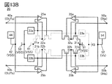
- 13A and 13B are circuit diagrams showing an example of an operation method of the communication device.
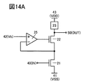
- 14A and 14B are circuit diagrams showing a configuration example of a semiconductor device.
- 15A and 15B are circuit diagrams showing a configuration example of a communication device.
- FIG. 16A is a circuit diagram showing a configuration example of a communication device.
- FIG. 16A is a circuit diagram showing a configuration example of a communication device.
- FIG. 16B is a circuit diagram showing a configuration example of the semiconductor device.
- FIG. 17 is a circuit diagram showing a configuration example of a communication device.
- 18A and 18B are circuit diagrams showing an example of an operation method of the communication device.
- FIG. 19 is a circuit diagram showing a configuration example of a semiconductor device.
- 20A and 20B are circuit diagrams showing a configuration example of a communication device.
- FIG. 21 is a diagram showing a configuration example of a semiconductor device.
- 22A and 22B are diagrams showing a configuration example of a transistor.
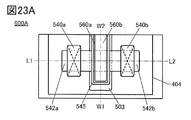
- 23A to 23C are diagrams showing a configuration example of a transistor.
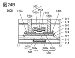
- 24A to 24C are diagrams showing a configuration example of a transistor.
- FIG. 25A is a diagram illustrating classification of the crystal structure of IGZO.
- FIG. 25A is a diagram illustrating classification of the crystal structure of IGZO.
- FIG. 25A is a diagram illustrating classification of the crystal structure of IGZO
- FIG. 25B is a diagram illustrating an XRD spectrum of the CAAC-IGZO film.
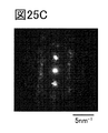
- FIG. 25C is a diagram for explaining the microelectron diffraction pattern of the CAAC-IGZO film.
- FIG. 26A is a top view of the semiconductor wafer.
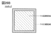
- FIG. 26B is an enlarged view of the chip.
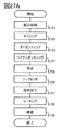
- FIG. 27A is a flowchart illustrating an example of a manufacturing process of electronic components.
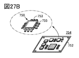
- FIG. 27B is a schematic perspective view of an electronic component.
- FIG. 28 is a diagram showing an example of an electronic device.
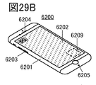
- 29A to 29F are diagrams showing an example of an electronic device.
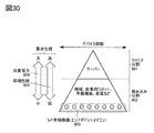
- FIG. 30 is a diagram showing the hierarchical structure of the IoT network and the tendency of the required specifications.
- FIG. 31 is an image diagram of factory automation.
- the position, size, range, etc. of each configuration shown in the drawings and the like may not represent the actual position, size, range, etc. in order to facilitate understanding of the invention. Therefore, the disclosed invention is not necessarily limited to the position, size, range, etc. disclosed in the drawings and the like.
- the resist mask or the like may be unintentionally reduced due to a process such as etching, but it may not be reflected in the drawing for easy understanding.
- top view also referred to as “plan view”
- perspective view etc.
- the description of some components may be omitted in order to make the drawing easier to understand.
- electrode and “wiring” in the present specification and the like do not functionally limit these components.
- an “electrode” may be used as part of a “wiring” and vice versa.
- the terms “electrode” and “wiring” include the case where a plurality of “electrodes” and “wiring” are integrally formed.
- the "terminal" in the electric circuit means a part where current input or output, voltage input or output, or signal reception or transmission is performed. Therefore, a part of the wiring or the electrode may function as a terminal.
- the terms “upper” and “lower” in the present specification and the like do not limit the positional relationship of the components to be directly above or directly below and to be in direct contact with each other.
- the electrode B does not have to be formed in direct contact with the insulating layer A, and another configuration is formed between the insulating layer A and the electrode B. Do not exclude those that contain elements.
- source and drain functions are interchanged depending on operating conditions, such as when transistors with different polarities are used or when the direction of current changes during circuit operation, so which one is the source or drain is limited. Is difficult. Therefore, in the present specification, the terms source and drain can be used interchangeably.
- electrically connected includes a case of being directly connected and a case of being connected via "something having some electrical action".
- the "thing having some kind of electrical action” is not particularly limited as long as it enables the exchange of electric signals between the connection targets. Therefore, even when it is expressed as “electrically connected", in an actual circuit, there is a case where there is no physical connection part and only the wiring is extended.
- the voltage often indicates the potential difference between a certain potential and a reference potential (for example, ground potential or source potential). Therefore, it is often possible to paraphrase voltage and potential. In the present specification and the like, voltage and potential can be paraphrased unless otherwise specified.
- semiconductor Even when the term "semiconductor” is used, for example, when the conductivity is sufficiently low, it has the characteristics of an "insulator". Therefore, it is possible to replace “semiconductor” with “insulator". In this case, the boundary between “semiconductor” and “insulator” is ambiguous, and it is difficult to make a strict distinction between the two. Therefore, the terms “semiconductor” and “insulator” described herein may be interchangeable.
- ordinal numbers such as “first" and “second” in the present specification and the like are added to avoid confusion of the components, and do not indicate any order or order such as process order or stacking order. ..
- terms that do not have ordinal numbers in the present specification and the like may have ordinal numbers within the scope of claims in order to avoid confusion of components.
- different ordinal numbers may be added within the scope of claims.
- the ordinal numbers may be omitted in the scope of claims and the like.
- the “on state” of the transistor means a state in which the source and drain of the transistor can be regarded as being electrically short-circuited.
- the “off state” of the transistor means a state in which the source and drain of the transistor can be regarded as being electrically cut off.
- the “on current” may mean a current flowing between the source and the drain when the transistor is in the on state.
- the “off current” may mean a current flowing between the source and the drain when the transistor is in the off state.
- gate refers to a part or all of the gate electrode and the gate wiring.
- the gate wiring refers to wiring for electrically connecting the gate electrode of at least one transistor with another electrode or another wiring.
- the source means a source region, a source electrode, and a part or all of the source wiring.
- the source region refers to a region of the semiconductor layer having a resistivity of a certain value or less.
- the source electrode refers to a conductive layer in a portion connected to the source region.
- the source wiring is a wiring for electrically connecting the source electrode of at least one transistor to another electrode or another wiring.
- the drain means a part or all of the drain region, the drain electrode, and the drain wiring.
- the drain region refers to a region of the semiconductor layer having a resistivity of a certain value or less.
- the drain electrode refers to a conductive layer at a portion connected to the drain region.
- Drain wiring refers to wiring for electrically connecting the drain electrode of at least one transistor to another electrode or another wiring.
- a metal oxide is a metal oxide in a broad sense. Metal oxides are classified into oxide insulators, oxide conductors (including transparent oxide conductors), oxide semiconductors (also referred to as Oxide Semiconductor or simply OS) and the like. For example, when a metal oxide is used in the active layer of a transistor, the metal oxide may be referred to as an oxide semiconductor. That is, when it is described as an OS transistor, it can be rephrased as a transistor having an oxide or an oxide semiconductor.
- FIG. 1 is a diagram showing a configuration example of a communication device 10 which is a communication device of one aspect of the present invention.
- the communication device 10 includes an antenna 11, an amplifier 12, an amplifier 13, a phase shifter 14, an amplifier 15, an inductor 16, and an inductor 17.
- the inductor is also called a coil. Further, the inductor 16 and the inductor 17 are provided so as to face each other.
- the communication device 10 has a function of performing wireless communication. For example, by exchanging and receiving signals between the communication device 10 and the base station, the information represented by the signals can be exchanged.
- the antenna 11 has a function of receiving a signal from the outside of the communication device 10. Further, the antenna 11 has a function of transmitting a signal to the outside of the communication device 10. For example, the antenna 11 has a function of receiving a signal transmitted as a radio wave by the base station. Further, for example, the antenna 11 has a function of transmitting a signal as a radio wave to the outside of the communication device 10.
- the signal transmitted and received by the communication device 10 can be a wave.
- a signal that is a wave may be referred to as a signal wave.
- the amplifier 12 has a function of amplifying the signal received by the antenna 11 and outputting it to the amplifier 13. Further, the amplifier 12 has a function of amplifying the signal input from the amplifier 13 and outputting it to the antenna 11.
- the amplifier 12 has a function as a power amplifier, and can significantly amplify the signal received by the antenna 11 and the signal input from the amplifier 13. Further, the amplifier 12 has a function as a low noise amplifier, and can amplify the signal received by the antenna 11 and the signal input from the amplifier 13 with high accuracy.
- the amplifier 13 has a function of amplifying the signal input from the amplifier 12 and outputting it to the phase shifter 14. Further, the amplifier 13 has a function of amplifying the signal input from the phase shifter 14 and outputting it to the amplifier 12.
- the amplifier 13 has a function as an RF (Radio Frequency) amplifier and can amplify a high frequency signal. Therefore, by providing the amplifier 13, the communication device 10 can send and receive high-frequency signals. Therefore, by providing the amplifier 13 in the communication device 10, the communication device 10 can perform wireless communication using, for example, a fifth generation mobile communication system (5G).
- 5G fifth generation mobile communication system
- the phase shifter 14 has a function of changing the phase shift of the signal. Since the communication device 10 has the phase shifter 14, the phase of the signal can be controlled with high accuracy even when the communication device 10 transmits and receives a high frequency signal. Therefore, beamforming can be performed even when the communication device 10 transmits and receives high-frequency signals. As a result, the communication device 10 can receive the signal transmitted from a distance. In addition, the communication device 10 can transmit a signal to a long distance. Therefore, by providing the phase shifter 14 in the communication device 10, the communication device 10 can perform wireless communication using, for example, 5G.
- the amplifier 15 has a function of amplifying the signal input from the phase shifter 14 and outputting it to the inductor 16. Further, the amplifier 15 has a function of amplifying the signal input from the inductor 16 and outputting it to the phase shifter 14. The amplifier 15 has a function as an isolation amplifier. Therefore, the noise contained in the signal input to the amplifier 15 can be removed.
- the signal input to the inductor 16 is supplied to the inductor 17 by electromagnetic induction.
- impedance matching can be performed.
- signal transmission can be performed efficiently.
- the wiring 19 has a function as a power supply line.
- the potential of the wiring 19 can be, for example, a low potential, for example, a ground potential.
- FIG. 2 is a diagram showing a configuration example of the amplifier circuit 20.
- the amplifier 12, the amplifier 13, the phase shifter 14, and the amplifier 15 shown in FIG. 1 can be configured to include an amplifier circuit 20.
- the amplifier circuit 20 includes a transistor 21a, a transistor 21b, a transistor 22a, a transistor 22b, a load 23a, a load 23b, a transistor 31a, a transistor 31b, a transistor 32a, a transistor 32b, a load 33a, and a load. It has 33b, a terminal 40a, a terminal 40b, a potential generation circuit 44, a terminal 50a, a terminal 50b, and a potential generation circuit 54.
- the potential generation circuit 44 and the potential generation circuit 54 may be provided outside the amplifier circuit 20.
- the transistor 21a, the transistor 21b, the transistor 22a, the transistor 22b, the transistor 31a, the transistor 31b, the transistor 32a, and the transistor 32b are all described as n-channel transistors.
- any or all of the above transistors may be used as p-channel transistors, if necessary or by appropriately changing the magnitude relationship of the potentials.
- the transistor 21a, the transistor 21b, the transistor 22a, the transistor 22b, the transistor 31a, the transistor 31b, the transistor 32a, and the transistor 32b may all be p-channel transistors.
- One of the source or drain of the transistor 21a is electrically connected to one of the source or drain of the transistor 22a.
- One of the source or drain of the transistor 21b is electrically connected to one of the source or drain of the transistor 22b.
- One of the source or drain of the transistor 31a is electrically connected to one of the source or drain of the transistor 32a.
- One of the source or drain of the transistor 31b is electrically connected to one of the source or drain of the transistor 32b.
- the other of the source or drain of the transistor 21a and the other of the source or drain of the transistor 21b are electrically connected to the wiring 41.
- the gate of the transistor 22a and the gate of the transistor 22b are electrically connected to the wiring 42.
- the other of the source or drain of the transistor 31a and the other of the source or drain of the transistor 31b are electrically connected to the wiring 51.
- the gate of the transistor 32a and the gate of the transistor 32b are electrically connected to the wiring 52.
- the potential generation circuit 44 is electrically connected to the wiring 42.
- the potential generation circuit 54 is electrically connected to the wiring 52.
- the terminal 40a is electrically connected to the gate of the transistor 21a, the source or drain of the transistor 32a, and the load 33a.
- the terminal 40b is electrically connected to the gate of the transistor 21b, the source or drain of the transistor 32b, and the load 33b.
- the terminal 50a is electrically connected to the gate of the transistor 31a, the source or drain of the transistor 22a, and the load 23a.
- the terminal 50b is electrically connected to the gate of the transistor 31b, the source or drain of the transistor 22b, and the load 23b.
- the load 23a and the load 23b are electrically connected to the wiring 43.
- the load 33a and the load 33b are electrically connected to the wiring 53.
- the wiring 41, the wiring 43, the wiring 51, and the wiring 53 have a function as a power supply line.
- the potentials of the wiring 41, the wiring 43, the wiring 51, and the wiring 53 can be, for example, constant potentials.
- the potentials of the wiring 41 and the wiring 51 can be set to a low potential
- the potentials of the wiring 43 and the wiring 53 can be set to a high potential.
- the power lines to which the same potential is supplied can be electrically connected to each other.
- the wiring 41 and the wiring 51 can be electrically connected to each other.
- the wiring 43 and the wiring 53 can be electrically connected to each other. That is, it may be said that the wiring 41 and the wiring 51 can be the same wiring, and the wiring 43 and the wiring 53 can be said to be the same wiring.
- a bias potential can be supplied to the wiring 42 and the wiring 52. Therefore, the transistor 22a, the transistor 22b, the transistor 32a, and the transistor 32b can function as a bias transistor.
- the bias potential can be a potential at which the transistor functioning as the bias transistor operates in the saturation region.
- the potential supplied to the wiring 42 can be generated by the potential generation circuit 44.
- the potential supplied to the wiring 52 can be generated by the potential generation circuit 54.
- a signal when a signal is input to the terminal 40a, a signal corresponding to the signal is output from the terminal 50a, and when a signal is input to the terminal 40b, the signal corresponding to the signal is output. It is output from the terminal 50b.
- the terminals 40a and 40b serve as input terminals
- the terminals 50a and 50b serve as output terminals.
- the signal corresponding to the signal when a signal is input to the terminal 50a, the signal corresponding to the signal is output from the terminal 40a, and when the signal is input to the terminal 50b, the signal corresponding to the signal is output from the terminal 40b. ..
- the terminals 40a and 40b serve as output terminals
- the terminals 50a and 50b serve as input terminals. From the above, it can be said that the terminals 40a, 40b, 50a, and 50b have both a function as an input terminal and a function as an output terminal.
- the ratio of the channel width to the channel length of the transistor 22a, the transistor 22b, the transistor 32a, and the transistor 32b that can function as a bias transistor is large.
- the ratio of the channel width of the transistor 22a to the channel length is preferably equal to or greater than the ratio of the channel width of the transistor 21a to the channel length.
- the ratio of the channel width of the transistor 22b to the channel length is preferably equal to or more than the ratio of the channel width of the transistor 21b to the channel length.
- the ratio of the channel width of the transistor 32a to the channel length is preferably equal to or more than the ratio of the channel width of the transistor 31a to the channel length.
- the ratio of the channel width of the transistor 32b to the channel length is preferably equal to or more than the ratio of the channel width of the transistor 31b to the channel length.
- the Miller effect can be suppressed by increasing the ratio of the channel width to the channel length of the transistor 22a, the transistor 22b, the transistor 32a, and the transistor 32b, which can function as a bias transistor.
- the product of the channel width and the channel length of the transistor 22a, the transistor 22b, the transistor 32a, and the transistor 32b that can function as a bias transistor is large.
- the product of the channel width of the transistor 22a and the channel length is preferably equal to or larger than the product of the channel width of the transistor 21a and the channel length.
- the product of the channel width of the transistor 22b and the channel length is preferably equal to or larger than the product of the channel width of the transistor 21b and the channel length.
- the product of the channel width of the transistor 32a and the channel length is preferably equal to or larger than the product of the channel width of the transistor 31a and the channel length.
- the product of the channel width of the transistor 32b and the channel length is preferably equal to or larger than the product of the channel width of the transistor 31b and the channel length. This is because the transistor 22a, the transistor 22b, the transistor 32a, and the transistor 32b, which can function as a bias transistor, do not deteriorate in frequency characteristics even if the channel length or the channel width is increased.
- the transistor 22a, the transistor 22b, the transistor 32a, and the transistor 32b that can function as a bias transistor have a large channel length.
- the channel length of the transistor 22a is preferably larger than the channel length of the transistor 21a.
- the channel length of the transistor 22b is preferably larger than the channel length of the transistor 21b.
- the channel length of the transistor 32a is preferably larger than the channel length of the transistor 31a.
- the channel length of the transistor 32b is preferably larger than the channel length of the transistor 31b.
- the voltage Vds which is the difference between the drain potential and the source potential of the transistor, becomes large.
- the gate potential is constant, an increase in the drain current flowing through the transistor can be suppressed.
- the threshold voltage of the transistor 21a is larger than the threshold voltage of the transistor 22a
- the threshold voltage of the transistor 21b is larger than the threshold voltage of the transistor 22b
- the threshold voltage of the transistor 31a is the transistor.
- the threshold voltage of the transistor 31b is larger than the threshold voltage of the 32a and is larger than the threshold voltage of the transistor 32b.
- the transistor 21a, the transistor 21b, the transistor 31a, and the transistor 31b are normally off, and the transistor 22a, the transistor 22b, the transistor 32a, and the transistor 32b are normally on.
- the gate-source voltage Vgs of the transistor 22a, the voltage Vgs of the transistor 22b, the voltage Vgs of the transistor 32a, and the voltage Vgs of the transistor 32b become smaller. Therefore, the range of the drain-source voltage Vds in which the transistor 22a, the transistor 22b, the transistor 32a, and the transistor 32b that can function as a bias transistor operate in the saturation region can be widened.
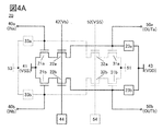
- FIG. 4A is an example of an operation method of the amplifier circuit 20 having the configuration shown in FIG. 2 when the terminal 40a is the input terminal INa, the terminal 40b is the input terminal INb, the terminal 50a is the output terminal OUTa, and the terminal 50b is the output terminal OUTb.
- FIG. 4B is an example of an operation method of the amplifier circuit 20 having the configuration shown in FIG. 2 when the terminal 50a is an input terminal INa, the terminal 50b is an input terminal INb, the terminal 40a is an output terminal OUTa, and the terminal 40b is an output terminal OUTb.
- a signal having a phase opposite to the signal input to the input terminal INa can be input to the input terminal INb.
- the potential VDD shows a high potential and the potential VSS shows a low potential.
- the same description is made in other figures.
- the potential of the wiring 42 is a bias potential Vb
- the potential of the wiring 52 is a low potential.
- the transistor 22a and the transistor 22b function as a bias transistor.
- the transistor 32a and the transistor 32b are turned off.
- transistors, loads, circuits, and wirings that do not contribute to the transmission of signals from the input terminal INa to the output terminal OUTa and from the input terminal INb to the output terminal OUTb are shown by dotted lines.
- the signal can be transmitted from the input terminal INa to the output terminal OUTa and the signal from the input terminal INb to the output terminal OUTb. Does not contribute.
- the transistor 32a and the transistor 32b are in the off state, no current flows through the transistor 31a and the transistor 31b, the signal is transmitted from the input terminal INa to the output terminal OUTa, and the signal is transmitted from the input terminal INb to the output terminal OUTb. Does not contribute to the transmission of signals.
- the load 33a is electrically connected to the other source or drain of the transistor 32a that is off, and is electrically connected to the other source or drain of the transistor 32b that is off.
- the load 33b also does not contribute to the transmission of the signal from the input terminal INa to the output terminal OUTa and the transmission of the signal from the input terminal INb to the output terminal OUTb. From the above, in FIG. 4A, the transistor 31a, the transistor 31b, the transistor 32a, the transistor 32b, the load 33a, and the load 33b, and a part of the circuit and wiring electrically connected to these are shown by dotted lines. ..
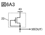
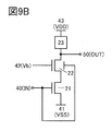
- FIG. 5A shows a transistor 21 (transistor 21a or transistor 21b), a transistor 22 (transistor 22a or transistor 22b), a load 23 (load 23a or load 23b), and a terminal 40 (terminal 40a or terminal 40b) shown in FIG. 4A. ), Wiring 41, wiring 42, wiring 43, and terminal 50 (terminal 50a or terminal 50b) are extracted.
- the terminal 40 is an input terminal IN (input terminal INa or input terminal INb), and the terminal 50 is an output terminal OUT (output terminal OUTa or output terminal OUTb).
- FIG. 5B is a diagram showing a circuit having a configuration in which the transistor 22 and the wiring 42 are omitted from the circuit shown in FIG. 5A.
- the terminal 50 is electrically connected to one of the source and drain of the transistor 21 and the load 23.
- the transistor 21 is an n-channel transistor. Further, the potential of the wiring 43 that is electrically connected to one of the source or drain of the transistor 21 via the load 23 is a high potential, and the wiring that is electrically connected to the other of the source or drain of the transistor 21. The potential of 41 is a low potential. Therefore, one of the source or drain of the transistor 21 can be a drain, and the other of the source or drain of the transistor 21 can be a source.
- the transconductance gm (Ids / Vgs, Ids is the drain current) of the transistor 21 becomes smaller than when the transistor 21 operates in the saturation region. Therefore, the amplification factor (also referred to as “gain” or “gain”) of the potential of the signal output from the output terminal OUT with respect to the potential of the signal input from the input terminal IN becomes small. Therefore, it is preferable that the transistor 21 is operated in the saturation region. From the above, if the potential of the input terminal IN becomes too large, the voltage Vds drops significantly and the transistor 21 operates in the linear region. Therefore, in order to operate the transistor 21 in the saturation region, the potential of the input terminal IN is set. It must be less than or equal to the specified value.
- the transistor 21 is an n-channel transistor as in the case shown in FIG. 5B
- one of the source or drain of the transistor 21 can be a drain, and the other of the source or drain of the transistor 21 can be a drain.
- one of the source or drain of the transistor 22 can be a source, and the other of the source or drain of the transistor 22 can be a drain.
- the transistor 21 and the transistor 22 are connected in series. Therefore, the magnitude of the drain current of the transistor 21 and the magnitude of the drain current of the transistor 22 are equal to each other. Therefore, the difference between the gate potential (bias potential Vb) of the transistor 22 and the source potential (drain potential of the transistor 21) is the gate potential (potential of the input terminal IN) and the source potential (low potential) of the transistor 21.
- the size corresponds to the difference between.
- the difference between the gate potential of the transistor 22 and the source potential is equal to the difference between the gate potential of the transistor 21 and the source potential. ..
- the electrical characteristics of the transistor 21 and the transistor 22 become the same.
- the voltage Vds which is the difference between the drain potential of the transistor 21 and the source potential, does not decrease as compared with the case shown in FIG. 5B. Therefore, the upper limit of the potential of the input terminal IN for operating the transistor 21 in the saturation region is larger than that shown in FIG. 5B.
- the amplifier circuit 20 since the amplifier circuit 20 has the transistor 22 capable of functioning as a bias transistor, the range of the potential of the signal that can be input to the input terminal IN can be widened. Therefore, the range of potentials of signals that can be transmitted and received by the communication device 10 can be widened.
- the potential of the wiring 42 is a low potential
- the potential of the wiring 52 is a bias potential.
- the transistor 22a and the transistor 22b are turned off.
- the transistor 32a and the transistor 32b function as a bias transistor.
- the transistor 22a and the transistor 22b are in the off state, they do not contribute to the transmission of the signal from the input terminal INa to the output terminal OUTa and the transmission of the signal from the input terminal INb to the output terminal OUTb. .. Further, since the transistor 22a and the transistor 22b are in the off state, no current flows through the transistor 21a and the transistor 21b, the signal is transmitted from the input terminal INa to the output terminal OUTa, and the signal is transmitted from the input terminal INb to the output terminal OUTb. Does not contribute to the transmission of signals.
- the load 23a is electrically connected to the other of the source or drain of the transistor 22a that is off, and is electrically connected to the other of the source or drain of the transistor 22b that is off.
- the load 23b also does not contribute to the transmission of the signal from the input terminal INa to the output terminal OUTa and the transmission of the signal from the input terminal INb to the output terminal OUTb. From the above, in FIG. 4B, the transistor 21a, the transistor 21b, the transistor 22a, the transistor 22b, the load 23a, and the load 23b, and a part of the circuit and wiring electrically connected to these are shown by dotted lines. ..
- FIGS. 6A1 to 6A4 are diagrams showing a configuration example of the load 23. Note that, in FIGS. 6A1 to 6A4, the wiring 43 and the terminal 50 are also shown for convenience of explanation.
- the load 23 may have a resistor. Further, as shown in FIG. 6A2, the load 23 may have a transistor. Further, as shown in FIG. 6A3, the load 23 may have a transistor, and the gate of the transistor may be electrically connected to the terminal 50. Further, as shown in FIG. 6A4, the load 23 may have a transistor, and the gate of the transistor may be electrically connected to the wiring 43.
- the transistor included in the load 23 is a p-channel transistor, and in FIG. 6A4, the transistor included in the load 23 is an n-channel transistor, but one aspect of the present invention is not limited to this. Even when the load 23 is shown in FIGS. 6A2 and 6A3, the transistor included in the load 23 may be an n-channel transistor. Further, even when the load 23 is shown in FIG. 6A4, the transistor included in the load 23 may be a p-channel transistor.
- a passive element may be provided between the transistor 21 and the wiring 41.
- the inductor 101 may be provided. In the configuration shown in FIG. 6B1, one terminal of the inductor 101 is electrically connected to the other of the source or drain of the transistor 21, and the other terminal of the inductor 101 is electrically connected to the wiring 41.
- the inductor 101 and the capacitance 102 may be provided.
- one terminal of the inductor 101 and one terminal of the capacitance 102 are electrically connected to the other of the source or drain of the transistor 21.
- the other terminal of the inductor 101 and the other terminal of the capacitance 102 are electrically connected to the wiring 41.
- the transistor 21 is the transistor 31 (transistor 31a or the transistor 31b), and the transistor 22 is the transistor 32 (transistor 32a or the transistor 32b).
- the load 23 is the load 33 (load 33a or the load 33b)
- the terminal 40 is the terminal 50
- the wiring 41 is the wiring 51
- the wiring 42 is the wiring 52
- the wiring 43 is the wiring 53
- the terminal 50 is the terminal.
- the conduction / non-conduction state between the wiring 41 and the terminals 50a and 50b can be switched by switching the potential of the wiring 42. Further, by switching the potential of the wiring 52, it is possible to switch the conduction / non-conduction state between the wiring 51 and the terminals 40a and 40b. From the above, the amplifier circuit 20 can be operated normally even if the switch 24 shown in FIG. 7A1 and the switch 34 shown in FIG. 7A2 are omitted. Specifically, when a signal is input to the terminals 40a and 40b, the signal corresponding to the signal can be output from the terminals 50a and 50b.
- the signal corresponding to the signal can be output from the terminals 40a and 40b.
- the switch 24 and the switch 34 may be provided.
- the potential of the wiring 42 and the potential of the wiring 52 can be fixed to the bias potential Vb.
- a transistor 28 may be provided as the switch 24, and a transistor 38 may be provided as the switch 34.
- one of the source or drain of the transistor 28 is electrically connected to the other of the source or drain of the transistor 21a and the other of the source or drain of the transistor 21b, and the source or drain of the transistor 28 is connected.
- the other side of the drain can be electrically connected to the wiring 41.
- one of the source or drain of the transistor 38 is electrically connected to the other of the source or drain of the transistor 31a and the other of the source or drain of the transistor 31b, and the source or drain of the transistor 38 is connected.
- the other of the above can be electrically connected to the wiring 51.
- the gate of the transistor 28 is electrically connected to the wiring 42
- the gate of the transistor 38 is electrically connected to the wiring 52. It can be configured to be connected to.
- the potential of the wiring 42 can be a bias potential Vb or a low potential.
- FIG. 8A is a diagram showing a configuration example of the amplifier circuit 20, and is a modification of the configuration shown in FIG.
- the gate of the transistor 22a and the gate of the transistor 22b are electrically connected to different wirings
- the gate of the transistor 32a and the gate of the transistor 32b are different wirings and electricity.
- the point that the amplifier circuit 20 is connected is different from the amplifier circuit 20 having the configuration shown in FIG.
- the gate of the transistor 22a and the potential generation circuit 44a are electrically connected via the wiring 42a. Further, the gate of the transistor 22b and the potential generation circuit 44b are electrically connected via the wiring 42b. Further, the gate of the transistor 32a and the potential generation circuit 54a are electrically connected via the wiring 52a. Further, the gate of the transistor 32b and the potential generation circuit 54b are electrically connected via the wiring 52b.
- the potential supplied to the wiring 42a can be generated by the potential generation circuit 44a, and the potential supplied to the wiring 42b can be generated by the potential generation circuit 44b. Further, the potential supplied to the wiring 52a can be generated by the potential generation circuit 54a, and the potential supplied to the wiring 52b can be generated by the potential generation circuit 54b.
- FIG. 8B is a diagram showing a configuration example of the amplifier circuit 20, and is a modification of the configuration shown in FIG.
- the amplifier circuit 20 having the configuration shown in FIG. 8B is different from the amplifier circuit 20 having the configuration shown in FIG. 2 in that the load 23a, the load 23b, the load 33a, the load 33b, the wiring 43, and the wiring 53 are not provided.
- FIG. 9A is a diagram showing a configuration example of the amplifier circuit 20, and is a modification of the configuration shown in FIG.
- the amplifier circuit 20 having the configuration shown in FIG. 9A is different from the amplifier circuit 20 having the configuration shown in FIG. 2 in that the transistor 22a, the transistor 22b, the transistor 32a, and the transistor 32b are provided with a back gate.
- gate may mean a front gate. Alternatively, it may indicate one or both of the front gate and the back gate.
- the back gate of the transistor 22a is electrically connected to the terminal 40a.
- the back gate of the transistor 22b is electrically connected to the terminal 40b.
- the back gate of the transistor 32a is electrically connected to the terminal 50a.
- the back gate of the transistor 32b is electrically connected to the terminal 50b.
- FIG. 9B is a diagram in which the transistor 21, the transistor 22, the load 23, the terminal 40, the wiring 41, the wiring 42, the wiring 43, and the terminal 50 shown in FIG. 9A are extracted.
- the terminal 40 is an input terminal IN
- the terminal 50 is an output terminal OUT.
- the increase width of the magnitude of the above can be made smaller than the increase width of the magnitude of the difference between the gate potential of the transistor 21 and the source potential.
- the circuit having the configuration shown in FIG. 9B can be applied to semiconductor devices other than communication devices.
- it can be used as a part of an amplifier circuit included in an operational amplifier.
- FIG. 10 is a diagram showing a configuration example of the amplifier 12. For convenience of explanation, the antenna 11 is also shown in FIG.
- the amplifier 12 may have a phase shifter 61, a capacitance 62, a switch 63, a phase shifter 64, an inductor 65, and an inductor 66.
- the inductor 65 and the inductor 66 are provided so as to face each other.
- the amplifier circuit 20 has the configuration shown in FIG.
- the configuration of the amplifier circuit 20 included in the amplifier 12 may be another configuration shown in the present embodiment. Further, the amplifier circuit 20 included in the amplifier 12 may have the configuration shown in the following embodiments.
- the antenna 11 is electrically connected to one terminal of the phase shifter 61.
- the other terminal of the phase shifter 61 is electrically connected to one terminal of the capacitance 62.
- One terminal of the capacitance 62 is electrically connected to one terminal of the phase shifter 64.
- the other terminal of the capacitance 62 is electrically connected to one terminal of the switch 63.
- the other terminal of the switch 63 is electrically connected to the wiring 73.
- the other terminal of the phase shifter 64 is electrically connected to one terminal of the inductor 65.
- the other terminal of the inductor 65 is electrically connected to the wiring 75.
- One terminal of the inductor 66 is electrically connected to the terminal 40a.
- the other terminal of the inductor 66 is electrically connected to the terminal 40b.
- the wiring 73 and the wiring 75 have a function as a power supply line.
- the potential of the wiring 73 and the potential of the wiring 75 can be, for example, a low potential, for example, a ground potential.
- FIG. 11 is a diagram showing a configuration example of the amplifier circuit 20, and is a modification of the configuration shown in FIG.
- the amplifier circuit 20 having the configuration shown in FIG. 11 is different from the amplifier circuit 20 having the configuration shown in FIG. 2 in that it has an operational amplifier 25a, an operational amplifier 25b, an operational amplifier 35a, and an operational amplifier 35b.
- the transistor 21a, the transistor 21b, the transistor 22a, the transistor 22b, the transistor 31a, the transistor 31b, the transistor 32a, and the transistor 32b are all n-channel transistors.
- any or all of the above transistors may be p-channel transistors.
- the transistor 21a, the transistor 21b, the transistor 22a, the transistor 22b, the transistor 31a, the transistor 31b, the transistor 32a, and the transistor 32b may all be p-channel transistors.
- One of the source or drain of the transistor 21a is electrically connected to one of the source or drain of the transistor 22a.
- One of the source or drain of the transistor 21b is electrically connected to one of the source or drain of the transistor 22b.
- One of the source or drain of the transistor 31a is electrically connected to one of the source or drain of the transistor 32a.
- One of the source or drain of the transistor 31b is electrically connected to one of the source or drain of the transistor 32b.
- the other of the source or drain of the transistor 21a and the other of the source or drain of the transistor 21b are electrically connected to the wiring 41.
- the other of the source or drain of the transistor 31a and the other of the source or drain of the transistor 31b are electrically connected to the wiring 51.
- the potential generation circuit 44 is electrically connected to the wiring 42.
- the potential generation circuit 54 is electrically connected to the wiring 52.
- the non-inverting input terminal of the operational amplifier 25a and the non-inverting input terminal of the operational amplifier 25b are electrically connected to the wiring 42.
- the non-inverting input terminal of the operational amplifier 35a and the non-inverting input terminal of the operational amplifier 35b are electrically connected to the wiring 52.
- the inverting input terminal of the operational amplifier 25a is electrically connected to one of the source or drain of the transistor 21a and one of the source or drain of the transistor 22a.
- the inverting input terminal of the operational amplifier 25b is electrically connected to one of the source or drain of the transistor 21b and one of the source or drain of the transistor 22b.
- the inverting input terminal of the operational amplifier 35a is electrically connected to one of the source or drain of the transistor 31a and one of the source or drain of the transistor 32a.
- the inverting input terminal of the operational amplifier 35b is electrically connected to one of the source or drain of the transistor 31b and one of the source or drain of the transistor 32b.
- the output terminal of the operational amplifier 25a is electrically connected to the gate of the transistor 22a.
- the output terminal of the operational amplifier 25b is electrically connected to the gate of the transistor 22b.
- the output terminal of the operational amplifier 35a is electrically connected to the gate of the transistor 32a.
- the output terminal of the operational amplifier 35b is electrically connected to the gate of the transistor 32b.
- the terminal 40a is electrically connected to the gate of the transistor 21a, the source or drain of the transistor 32a, and the load 33a.
- the terminal 40b is electrically connected to the gate of the transistor 21b, the source or drain of the transistor 32b, and the load 33b.
- the terminal 50a is electrically connected to the gate of the transistor 31a, the source or drain of the transistor 22a, and the load 23a.
- the terminal 50b is electrically connected to the gate of the transistor 31b, the source or drain of the transistor 22b, and the load 23b.
- the load 23a and the load 23b are electrically connected to the wiring 43.
- the load 33a and the load 33b are electrically connected to the wiring 53.
- the potential of the output terminal changes so that the potential of the non-inverting input terminal and the potential of the inverting input terminal become equal. Therefore, when a predetermined potential is supplied to the non-inverting input terminal of the operational amplifier, the potential of the output terminal of the operational amplifier becomes a potential corresponding to the predetermined potential. Therefore, when the bias potential is supplied to the wiring 42, the transistor 22a and the transistor 22b function as a bias transistor. Further, when the bias potential is supplied to the wiring 52, the transistor 32a and the transistor 32b function as a bias transistor.
- the bias potential can be the potential at which the transistor functioning as the bias transistor operates in the saturation region.
- FIG. 13A is an example of an operation method of the amplifier circuit 20 having the configuration shown in FIG. 11 when the terminal 40a is the input terminal INa, the terminal 40b is the input terminal INb, the terminal 50a is the output terminal OUTa, and the terminal 50b is the output terminal OUTb.
- FIG. 13B is an example of an operation method of the amplifier circuit 20 having the configuration shown in FIG. 11 when the terminal 50a is the input terminal INa, the terminal 50b is the input terminal INb, the terminal 40a is the output terminal OUTa, and the terminal 40b is the output terminal OUTb.
- a signal having a phase opposite to the signal input to the input terminal INa can be input to the input terminal INb.
- Terminal 40 terminal 40a or terminal 40b
- wiring 41, wiring 42, wiring 43, and terminal 50 terminal 50a or terminal 50b
- the terminal 40 is an input terminal IN (input terminal INa or input terminal INb)
- the terminal 50 is an output terminal OUT (output terminal OUTa or output terminal OUTb).
- FIG. 14B is a diagram showing a circuit having a configuration in which the transistor 22, the operational amplifier 25, and the wiring 42 are omitted from the circuit shown in FIG. 14A.
- the terminal 50 is electrically connected to either the source or drain of the transistor 21 and the load 23.
- the configuration shown in FIG. 14B is the same as the configuration shown in FIG. 5B.
- the potential of the input terminal IN needs to be set to a predetermined value or less.
- the transistor 21 is an n-channel transistor as in the case shown in FIGS. 5B and 14B
- one of the source and drain of the transistor 21 can be a drain, and the source or drain of the transistor 21 can be used.
- the other of the drains can be the source.
- one of the source or drain of the transistor 22 can be a source, and the other of the source or drain of the transistor 22 can be a drain.
- the drain of the transistor 21 is electrically connected to the inverting input terminal of the operational amplifier 25, and the bias potential Vb is supplied to the non-inverting input terminal of the operational amplifier 25. Therefore, even if the on-resistance of the transistor 21 decreases, the decrease in the drain potential of the transistor 21 can be suppressed.
- the drain potential of the transistor 21 can be a bias potential Vb. Therefore, the upper limit of the potential of the input terminal IN for operating the transistor 21 in the saturation region is larger than that shown in FIG. 14B.
- the amplifier circuit 20 includes the transistor 22 capable of functioning as a bias transistor and the operational amplifier 25, the range of the potential of the signal that can be input to the input terminal IN can be widened. Therefore, the range of potentials of signals that can be transmitted and received by the communication device 10 can be widened.
- FIG. 15A is a diagram showing a configuration example of the amplifier circuit 20, and is a modification of the configuration shown in FIG.
- the non-inverting input terminal of the operational amplifier 25a and the non-inverting input terminal of the operational amplifier 25b are electrically connected to different wirings, and the non-inverting input terminal of the operational amplifier 35a and the operational amplifier 35b are connected.
- the amplifier circuit 20 having the configuration shown in FIG. 11 in that the non-inverting input terminal of No. 1 is electrically connected to a different wiring.
- the non-inverting input terminal of the operational amplifier 25a and the potential generation circuit 44a are electrically connected via the wiring 42a. Further, the non-inverting input terminal of the operational amplifier 25b and the potential generation circuit 44b are electrically connected via the wiring 42b. Further, the non-inverting input terminal of the operational amplifier 35a and the potential generation circuit 54a are electrically connected via the wiring 52a. Further, the non-inverting input terminal of the operational amplifier 35b and the potential generation circuit 54b are electrically connected via the wiring 52b.
- FIG. 15B is a diagram showing a configuration example of the amplifier circuit 20, and is a modification of the configuration shown in FIG.
- the amplifier circuit 20 having the configuration shown in FIG. 15B is different from the amplifier circuit 20 having the configuration shown in FIG. 11 in that the load 23a, the load 23b, the load 33a, the load 33b, the wiring 43, and the wiring 53 are not provided.
- FIG. 16A is a diagram showing a configuration example of the amplifier circuit 20, and is a modification of the configuration shown in FIG.
- the amplifier circuit 20 having the configuration shown in FIG. 16A is different from the amplifier circuit 20 having the configuration shown in FIG. 11 in that the transistor 22a, the transistor 22b, the transistor 32a, and the transistor 32b are provided with a back gate.
- the back gate of the transistor 22a is electrically connected to the terminal 40a.
- the back gate of the transistor 22b is electrically connected to the terminal 40b.
- the back gate of the transistor 32a is electrically connected to the terminal 50a.
- the back gate of the transistor 32b is electrically connected to the terminal 50b.
- FIG. 16B is a diagram in which the transistor 21, the transistor 22, the load 23, the operational amplifier 25, the terminal 40, the wiring 41, the wiring 42, the wiring 43, and the terminal 50 shown in FIG. 16A are extracted.
- the terminal 40 is an input terminal IN
- the terminal 50 is an output terminal OUT.
- the increase width of the magnitude of the above can be made smaller than the increase width of the magnitude of the difference between the gate potential of the transistor 21 and the source potential.
- the circuit having the configuration shown in FIG. 16B can be applied to semiconductor devices other than communication devices.
- it can be used as a part of an amplifier circuit included in an operational amplifier.
- FIG. 17 is a diagram showing a configuration example of the amplifier circuit 20.
- the amplifier circuit 20 shown in FIG. 17 includes a transistor 21a, a transistor 21b, a transistor 22a, a transistor 22b, a load 23a, a load 23b, an operational amplifier 25a, an operational amplifier 25b, a transistor 31a, a transistor 31b, a transistor 32a, a transistor 32b, a load 33a, and a load 33b.
- the memory circuit 80 can be configured to have a transistor 81 and a capacity 82.
- the memory circuit 90 can be configured to have a transistor 91 and a capacity 92.
- One of the source or drain of the transistor 21a is electrically connected to one of the source or drain of the transistor 22a.
- One of the source or drain of the transistor 22a is electrically connected to one terminal of the switch 27a.
- One of the source or drain of the transistor 21b is electrically connected to one of the source or drain of the transistor 22b.
- One of the source or drain of the transistor 22b is electrically connected to one terminal of the switch 27b.
- One of the source or drain of the transistor 31a is electrically connected to one of the source or drain of the transistor 32a.
- One of the source or drain of the transistor 32a is electrically connected to one terminal of the switch 37a.
- One of the source or drain of the transistor 31b is electrically connected to one of the source or drain of the transistor 32b.
- One of the source or drain of the transistor 32b is electrically connected to one terminal of the switch 37b.
- the other of the source or drain of the transistor 21a and the other of the source or drain of the transistor 21b are electrically connected to the wiring 41.
- the other of the source or drain of the transistor 31a and the other of the source or drain of the transistor 31b are electrically connected to the wiring 51.
- the non-inverting input terminal of the operational amplifier 25a and the non-inverting input terminal of the operational amplifier 25b are electrically connected to the wiring 42.
- the non-inverting input terminal of the operational amplifier 35a and the non-inverting input terminal of the operational amplifier 35b are electrically connected to the wiring 52.
- the inverting input terminal of the operational amplifier 25a is electrically connected to one terminal of the switch 26a and the other terminal of the switch 27a.
- the inverting input terminal of the operational amplifier 25b is electrically connected to one terminal of the switch 26b and the other terminal of the switch 27b.
- the inverting input terminal of the operational amplifier 35a is electrically connected to one terminal of the switch 36a and the other terminal of the switch 37a.
- the inverting input terminal of the operational amplifier 35b is electrically connected to one terminal of the switch 36b and the other terminal of the switch 37b.
- the output terminal of the operational amplifier 25a is electrically connected to the gate of the transistor 22a.
- the output terminal of the operational amplifier 25b is electrically connected to the gate of the transistor 22b.
- the output terminal of the operational amplifier 35a is electrically connected to the gate of the transistor 32a.
- the output terminal of the operational amplifier 35b is electrically connected to the gate of the transistor 32b.
- the other terminal of the switch 26a is electrically connected to the wiring 46a.
- the other terminal of the switch 26b is electrically connected to the wiring 46b.
- the other terminal of the switch 36a is electrically connected to the wiring 56a.
- the other terminal of the switch 36b is electrically connected to the wiring 56b.
- the terminal 40a is electrically connected to the gate of the transistor 21a, the source or drain of the transistor 32a, and the load 33a.
- the terminal 40b is electrically connected to the gate of the transistor 21b, the source or drain of the transistor 32b, and the load 33b.
- the terminal 50a is electrically connected to the gate of the transistor 31a, the source or drain of the transistor 22a, and the load 23a.
- the terminal 50b is electrically connected to the gate of the transistor 31b, the source or drain of the transistor 22b, and the load 23b.
- the load 23a and the load 23b are electrically connected to the wiring 43.
- the load 33a and the load 33b are electrically connected to the wiring 53.
- the wiring 42 is electrically connected to the memory circuit 80. Specifically, the wiring 42 is electrically connected to one of the source or drain of the transistor 81 and one of the terminals of the capacitance 82. Further, the other side of the source or drain of the transistor 81 is electrically connected to the potential generation circuit 44, and the gate of the transistor 81 is electrically connected to the wiring 84. Further, the other terminal of the capacitance 82 is electrically connected to the wiring 85.
- the wiring 52 is electrically connected to the memory circuit 90. Specifically, the wiring 52 is electrically connected to one of the sources and drains of the transistor 91 and one terminal of the capacitance 92. Further, the other side of the source or drain of the transistor 91 is electrically connected to the potential generation circuit 54, and the gate of the transistor 91 is electrically connected to the wiring 94. Further, the other terminal of the capacitance 92 is electrically connected to the wiring 85.
- the wiring 46a, the wiring 46b, the wiring 56a, the wiring 56b, the wiring 85, and the wiring 95 have a function as a power supply line.
- the potentials of the wiring 46a, the wiring 46b, the wiring 56a, the wiring 56b, the wiring 85, and the wiring 95 can be, for example, constant potentials.
- the potentials of the wiring 46a, the wiring 46b, the wiring 56a, and the wiring 56b can be set to a high potential, and the potentials of the wiring 85 and the wiring 95 can be set to a low potential.
- the memory circuit 80 has a function of holding the potential of the wiring 42.
- the memory circuit 90 has a function of holding the potential of the wiring 52.
- the transistor 81 included in the memory circuit 80 has a function of controlling the supply of electric potential to the wiring 42. Specifically, the potential that turns on the transistor 81 is supplied to the wiring 84, and the potential generation circuit 44 and the wiring 42 are made conductive. Then, the potential generated by the potential generation circuit 44 is supplied to the wiring 42.
- the potential generated by the potential generation circuit 44 can be a bias potential Vb. Therefore, the bias potential Vb can be supplied to the wiring 42.
- the potential for turning off the transistor 81 is supplied to the wiring 84. By turning off the transistor 81, the potential of the wiring 42 can be maintained.
- the transistor 81 is preferably a transistor (OS transistor) in which a metal oxide is used for the active layer. Since the oxide semiconductor, which is a kind of metal oxide, has a band gap of 2 eV or more, the off-current is remarkably small. By using the transistor 81 as an OS transistor, the potential of the wiring 42 can be maintained for a long period of time.
- OS transistor transistor
- the memory circuit 80 can be referred to as an "OS memory".
- the OS memory can retain the written information for a period of one year or more, or even ten years or more, even if the power supply is stopped. Therefore, the OS memory can be regarded as a non-volatile memory.
- the OS memory is a method of writing an electric charge to a node via an OS transistor, a high voltage required for a conventional flash memory is not required, and a high-speed writing operation can be realized. Also, since no charge is injected or withdrawn into the floating gate or charge capture layer, the OS memory is capable of writing and reading data virtually unlimited times. The OS memory has less deterioration than the conventional flash memory, and high reliability can be obtained.
- the OS memory does not undergo a structural change at the atomic level like a magnetic memory or a resistance change type memory. Therefore, the OS memory is superior in rewrite resistance to the magnetic memory and the resistance change type memory.
- the memory circuit 80 is the memory circuit 90
- the transistor 81 is the transistor 91
- the capacity 82 is the capacity 92
- the potential generation circuit 44 is the potential generation circuit 54
- the wiring 42 is the wiring 52.
- FIG. 18A is an example of an operation method of the amplifier circuit 20 having the configuration shown in FIG. 17 when the terminal 40a is the input terminal INa, the terminal 40b is the input terminal INb, the terminal 50a is the output terminal OUTa, and the terminal 50b is the output terminal OUTb.
- FIG. 18B is an example of an operation method of the amplifier circuit 20 having the configuration shown in FIG. 17 when the terminal 50a is an input terminal INa, the terminal 50b is an input terminal INb, the terminal 40a is an output terminal OUTa, and the terminal 40b is an output terminal OUTb. It is a figure which shows.
- the memory 80 and the memory 90 are preliminarily held with electric charges so that the potentials of the wiring 42 and the wiring 52 become the bias potential Vb.
- the switch 26a, the switch 26b, the switch 37a, and the switch 37b are turned off.
- the potential of the inverting input terminal of the operational amplifier 35a and the potential of the inverting input terminal of the operational amplifier 35b become high potentials.
- the potentials of the non-inverting input terminal of the operational amplifier 35a and the non-inverting input terminal of the operational amplifier 35b are the bias potential Vb, which is lower than the high potential.
- the switch 37a and the switch 37b are in the off state, the operational amplifier 35a and the operational amplifier 35b are not fed back. From the above, in the state shown in FIG. 18A, the operational amplifier 35a and the operational amplifier 35b function as comparators.
- the potential of the inverting input terminal of the operational amplifier 35a is higher than the potential of the non-inverting input terminal of the operational amplifier 35a
- the potential of the inverting input terminal of the operational amplifier 35b is higher than the potential of the non-inverting input terminal of the operational amplifier 35b. Therefore, the operational amplifier 35a and the operational amplifier 35b output, for example, a low potential. Therefore, since the gate potential of the transistor 32a and the gate potential of the transistor 32b are low potentials, the transistor 32a and the transistor 32b are turned off.
- transistors, loads, switches, circuits, and wirings that do not contribute to the transmission of signals from the input terminal INa to the output terminal OUTa and from the input terminal INb to the output terminal OUTb are shown by dotted lines. ..
- the switch 26a, the switch 26b, the transistor 32a, the transistor 32b, the switch 37a, and the switch 37b are in the off state, the signal is transmitted from the input terminal INa to the output terminal OUTa, and It does not contribute to the transmission of signals from the input terminal INb to the output terminal OUTb.
- the transistor 32a and the transistor 32b are in the off state, no current flows through the transistor 31d and the transistor 31b, the signal is transmitted from the input terminal INa to the output terminal OUTa, and the signal is transmitted from the input terminal INb to the output terminal OUTb. Does not contribute to the transmission of signals.
- the load 33a is electrically connected to the other source or drain of the transistor 32a that is off, and is electrically connected to the other source or drain of the transistor 32b that is off.
- the load 33b also does not contribute to the transmission of the signal from the input terminal INa to the output terminal OUTa and the transmission of the signal from the input terminal INb to the output terminal OUTb. From the above, in FIG.
- the switch 27a, the switch 27b, the switch 36a, and the switch 36b are turned off.
- the potential of the inverting input terminal of the operational amplifier 25a and the potential of the inverting input terminal of the operational amplifier 25b become high potentials.
- the potentials of the non-inverting input terminal of the operational amplifier 25a and the non-inverting input terminal of the operational amplifier 25b are the bias potential Vb, which is lower than the high potential.
- the switch 27a and the switch 27b are in the off state, the operational amplifier 25a and the operational amplifier 25b are not fed back. From the above, in the state shown in FIG. 18B, the operational amplifier 35a and the operational amplifier 35b function as comparators.
- the potential of the inverting input terminal of the operational amplifier 25a is higher than the potential of the non-inverting input terminal of the operational amplifier 25a
- the potential of the inverting input terminal of the operational amplifier 25b is higher than the potential of the non-inverting input terminal of the operational amplifier 25b. Therefore, the operational amplifier 25a and the operational amplifier 25b output, for example, a low potential. Therefore, since the gate potential of the transistor 22a and the gate potential of the transistor 22b are low potentials, the transistor 22a and the transistor 22b are turned off.
- the switch 27a, the switch 27b, the transistor 22a, the transistor 22b, the switch 36a, and the switch 36b are in the off state, the signal is transmitted from the input terminal INa to the output terminal OUTa and the input terminal. It does not contribute to the transmission of signals from INb to the output terminal OUTb. Further, since the transistor 22a and the transistor 22b are in the off state, no current flows through the transistor 21a and the transistor 21b, the signal is transmitted from the input terminal INa to the output terminal OUTa, and the signal is transmitted from the input terminal INb to the output terminal OUTb. Does not contribute to the transmission of signals.
- the load 23a is electrically connected to the other of the source or drain of the transistor 22a that is off, and is electrically connected to the other of the source or drain of the transistor 22b that is off.
- the load 23b also does not contribute to the transmission of the signal from the input terminal INa to the output terminal OUTa and the transmission of the signal from the input terminal INb to the output terminal OUTb. From the above, in FIG. 18B, the transistor 21a, the transistor 21b, the transistor 22a, the transistor 22b, the load 23a, the load 23b, the switch 27a, the switch 27b, the switch 36a, and the switch 36b, and the circuit electrically connected thereto A part of the wiring is shown by a dotted line.
- FIGS. 14A and 14B can also be applied to the case where the amplifier circuit 20 has the configuration shown in FIG. Further, the configuration shown in FIG. 16A and the description shown in FIG. 16B can also be applied when the amplifier circuit 20 has the configuration shown in FIG. Specifically, a back gate can be provided in the transistor 22a, the transistor 22b, the transistor 32a, and the transistor 32b included in the amplifier circuit 20 having the configuration shown in FIG.
- the back gate of the transistor 22a is electrically connected to the terminal 40a
- the back gate of the transistor 22b is electrically connected to the terminal 40b
- the back gate of the transistor 32a is electrically connected to the terminal 50a.
- the back gate connected and included in the transistor 32b can be configured to be electrically connected to the terminal 50b.
- FIG. 19 shows a transistor 21 (transistor 21a or transistor 21b), a transistor 22 (transistor 22a or transistor 22b), a load 23 (load 23a or load 23b), and an operational device 25 (operator 25a or operational device 25b) shown in FIG. 18A. ), Switch 26 (switch 26a or switch 26b), switch 27 (switch 27a or switch 27b), terminal 40 (terminal 40a or terminal 40b), wiring 41, wiring 42, wiring 43, and terminal 50 (terminal 50a). , Or the terminal 50b) is extracted.
- the terminal 40 is an input terminal IN (input terminal INa or input terminal INb), and the terminal 50 is an output terminal OUT (output terminal OUTa or output terminal OUTb).
- the circuit having the configuration shown in FIG. 19 can be applied to semiconductor devices other than communication devices.
- it can be used as a part of an amplifier circuit included in an operational amplifier.
- FIG. 20A is a diagram showing a configuration example of the amplifier circuit 20, and is a modification of the configuration shown in FIG.
- the amplifier circuit 20 having the configuration shown in FIG. 13A is different from the amplifier circuit 20 having the configuration shown in FIG. 17 in that it does not have the memory circuit 80 and the memory circuit 90.
- the potential generation circuit 44 and the potential generation circuit 54 generate the bias potential Vb.
- the potentials of the wiring 42 and the wiring 52 are set as the bias potential Vb.
- FIG. 20B is a diagram showing a configuration example of the amplifier circuit 20, and is a modification of the configuration shown in FIG.
- the non-inverting input terminal of the operational amplifier 25a and the non-inverting input terminal of the operational amplifier 25b, and the non-inverting input terminal of the operational amplifier 35a and the non-inverting input terminal of the operational amplifier 35b are electrically connected to each other.
- the point that it is connected is different from the amplifier circuit 20 having the configuration shown in FIG. Further, it is different from the amplifier circuit 20 having the configuration shown in FIG. 17 in that the memory circuit 90 and the potential generation circuit 54 are not provided.
- the non-inverting input terminal of the operational amplifier 25a, the non-inverting input terminal of the operational amplifier 25b, the non-inverting input terminal of the operational amplifier 35a, and the non-inverting input terminal of the operational amplifier 35b are electrically connected to the memory circuit 80. Is connected.
- the non-inverting input terminal of the operational amplifier 25a, the non-inverting input terminal of the operational amplifier 25b, the non-inverting input terminal of the operational amplifier 35a, and the non-inverting input terminal of the operational amplifier 35b are one of the source and drain of the transistor 81 and the capacitance. It is electrically connected to one of the terminals of 82.
- FIG. 21 shows a part of the cross-sectional structure of the semiconductor device included in the communication device of one aspect of the present invention or the semiconductor device of one aspect of the present invention.
- the semiconductor device having the configuration shown in FIG. 21 includes a transistor 550 and a transistor 500.
- a cross-sectional view of the transistor 500 and the transistor 550 in the channel length direction is shown in FIG. 22A
- a cross-sectional view of the transistor 500 and the transistor 550 in the channel width direction is shown in FIG. 22B.
- the transistor 500 corresponds to the transistor 21 shown in the above embodiment
- the transistor 550 corresponds to the transistor 22 shown in the above embodiment.
- the transistor 500 and the transistor 550 can be OS transistors.
- one or both of the transistor 500 and the transistor 550 may be a transistor other than the OS transistor.
- one or both of the transistor 500 and the transistor 550 may be a transistor (Si transistor) using silicon as the active layer.
- the transistor 500 is provided above the transistor 550.
- the transistor 500 and the transistor 550 may be provided on the same layer.
- the transistor 500 and the transistor 550 were arranged on the insulator 513 and the conductor 503 arranged to be embedded in the insulator 514 and the insulator 516 and the conductor 503.
- An insulator 580 having an opening formed by superimposing between the two, an insulator 545 arranged so as to have a region in contact with the bottom surface and the side surface of the opening, and a conductor 560 arranged on the forming surface of the insulator 545.
- the insulator 544 is arranged between the oxide 530a, the oxide 530b, the conductor 542a, and the conductor 542b and the insulator 580.
- the conductor 560 includes a conductor 560a provided inside the insulator 545 and a conductor 560b provided so as to be embedded inside the conductor 560a. It is preferable to have.
- the insulator 574 is arranged on the insulator 580, the conductor 560, and the insulator 545.
- oxide 530a and oxide 530b may be collectively referred to as oxide 530.
- the transistor 500 and the transistor 550 show a configuration in which two layers of oxide 530a and oxide 530b are laminated in a region where a channel is formed and in the vicinity thereof, but the present invention is limited to this. is not.
- a single layer of the oxide 530b or a laminated structure of three or more layers may be provided.
- the conductor 560 is shown as a two-layer laminated structure, but the present invention is not limited to this.
- the conductor 560 may have a single-layer structure or a laminated structure of three or more layers.
- the transistor 500 and the transistor 550 shown in FIGS. 21 and 22A and 22B are examples, and the transistor is not limited to the configuration, and an appropriate transistor may be used depending on the circuit configuration, driving method, and the like.
- the conductor 560 functions as a gate electrode of the transistor, and the conductor 542a and the conductor 542b function as a source electrode or a drain electrode, respectively.
- the conductor 560 is formed so as to be embedded in the opening of the insulator 580 and the region sandwiched between the conductor 542a and the conductor 542b.
- the arrangement of the conductor 560, the conductor 542a and the conductor 542b is self-aligned with respect to the opening of the insulator 580. That is, in the transistor 500 and the transistor 550, the gate electrode can be arranged in a self-aligned manner between the source electrode and the drain electrode. Therefore, since the conductor 560 can be formed without providing the alignment margin, the occupied area of the transistor 500 and the transistor 550 can be reduced. As a result, the semiconductor device can be miniaturized and highly integrated.
- the conductor 560 is formed in a region between the conductor 542a and the conductor 542b in a self-aligned manner, the conductor 560 does not have a region that overlaps with the conductor 542a or the conductor 542b. Thereby, the parasitic capacitance formed between the conductor 560 and the conductors 542a and 542b can be reduced. Therefore, the switching speed of the transistor 500 and the transistor 550 can be improved, and the frequency characteristics can be improved.
- the conductor 560 may function as a first gate (also referred to as a top gate) electrode. Further, the conductor 503 may function as a second gate (also referred to as a bottom gate) electrode. Further, the conductor 560 may function as a front gate electrode, and the conductor 503 may function as a back gate electrode.
- the threshold voltage of the transistor 500 and the transistor 550 can be controlled by changing the potential applied to the conductor 503 independently without interlocking with the potential applied to the conductor 560. In particular, by applying a negative potential to the conductor 503, the threshold voltage of the transistor 500 and the transistor 550 can be made larger than 0V, and the off-current can be reduced. Therefore, when a negative potential is applied to the conductor 503, the drain current when the potential applied to the conductor 560 is 0 V can be made smaller than when it is not applied.
- the conductor 503 is arranged so as to overlap the oxide 530 and the conductor 560. As a result, when a potential is applied to the conductor 560 and the conductor 503, the electric field generated from the conductor 560 and the electric field generated from the conductor 503 are connected to cover the channel forming region formed in the oxide 530. Can be done.
- the configuration of a transistor that electrically surrounds a channel forming region by an electric field of a pair of gate electrodes is referred to as a surroundd channel (s-channel) configuration.
- a surroundd channel (s-channel) configuration the configuration of a transistor that electrically surrounds a channel forming region by an electric field of a pair of gate electrodes (a first gate electrode and a second gate electrode) is referred to as a surroundd channel (s-channel) configuration.
- the side surface and the periphery of the oxide 530 in contact with the conductor 542a and the conductor 542b functioning as the source electrode and the drain electrode are said to be type I as in the channel formation region. It has characteristics.
- the side surface and the periphery of the oxide 530 in contact with the conductor 542a and the conductor 542b are in contact with the insulator 544, it can be type I as in the channel forming region.
- type I can be treated as the same as high-purity authenticity described later.
- the s-channel configuration disclosed in the present specification and the like is different from the Fin type configuration and the planar type configuration. By adopting the s-channel configuration, it is possible to increase the resistance to the short-channel effect, in other words, to make a transistor in which the short-channel effect is unlikely to occur.
- the conductor 503 can be configured to have the conductor 503a and the conductor 503b.
- the conductor 503a is formed in contact with the inner walls of the openings of the insulator 514 and the insulator 516, and the conductor 503b is further formed inside.
- the conductor 503 is configured such that the conductor 503a and the conductor 503b are laminated, but the present invention is not limited to this.
- the conductor 503 may be provided as a single layer or a laminated structure having three or more layers.
- the conductor 503a it is preferable to use a conductive material having a function of suppressing the diffusion of impurities such as hydrogen atoms, hydrogen molecules, water molecules, and copper atoms (the above impurities are difficult to permeate).
- a conductive material having a function of suppressing the diffusion of oxygen for example, at least one oxygen atom, oxygen molecule, etc.
- the function of suppressing the diffusion of impurities or oxygen is a function of suppressing the diffusion of any one or all of the above impurities or the above oxygen.
- the conductor 503a since the conductor 503a has a function of suppressing the diffusion of oxygen, it is possible to prevent the conductor 503b from being oxidized and the conductivity from being lowered.
- the conductor 503 also functions as a wiring, it is preferable to use a highly conductive conductive material containing tungsten, copper, or aluminum as a main component for the conductor 503b.
- the insulator 520, the insulator 522, and the insulator 524 have a function as a gate insulating film for the conductor 503.
- the insulator 524 in contact with the oxide 530 it is preferable to use an insulator containing more oxygen than oxygen satisfying the stoichiometric composition.
- the oxygen is easily released from the membrane by heating.
- oxygen released by heating may be referred to as "excess oxygen”. That is, it is preferable that the insulator 524 is formed with a region containing excess oxygen (also referred to as “excess oxygen region”).
- the defective (hereinafter sometimes referred to as V O H) serves as a donor, sometimes electrons serving as carriers are generated.
- a part of hydrogen may be combined with oxygen that is bonded to a metal atom to generate an electron as a carrier. Therefore, a transistor using an oxide semiconductor containing a large amount of hydrogen tends to have a normally-on characteristic. Further, since hydrogen in the oxide semiconductor easily moves due to stress such as heat and electric field, if the oxide semiconductor contains a large amount of hydrogen, the reliability of the transistor may deteriorate.
- the V O H to obtain a sufficiently reduced oxide semiconductor, the moisture in the oxide semiconductor, the removal of impurities such as hydrogen (also referred to as “dewatering” or “dehydrogenation process") It is important to supply oxygen to the oxide semiconductor to compensate for the oxygen deficiency (also referred to as “oxygenation treatment”).
- the V O H such as an oxide semiconductor in which impurities are sufficiently reduced in by using a channel formation region of the transistor, it is possible to have stable electrical characteristics.
- the insulator having an excess oxygen region it is preferable to use an oxide material in which a part of oxygen is desorbed by heating.
- Oxides that desorb oxygen by heating are those in which the amount of oxygen desorbed in terms of oxygen atoms is 1.0 ⁇ 10 18 atoms / cm 3 or more in TDS (Thermkesortion Spectroscopy) analysis, preferably 1.
- the surface temperature of the film during the TDS analysis is preferably in the range of 100 ° C. or higher and 700 ° C. or lower, or 100 ° C. or higher and 400 ° C. or lower.
- the insulator having the excess oxygen region and the oxide 530 may be brought into contact with each other to perform one or more of heat treatment, microwave treatment, or RF treatment.
- heat treatment microwave treatment, or RF treatment.
- water or hydrogen in the oxide 530 can be removed.
- reactions occur which bonds VoH is disconnected, when other words happening reaction of "V O H ⁇ Vo + H", it can be dehydrogenated.
- the hydrogen generated as oxygen combines with H 2 O, it may be removed from the oxide 530 or oxide 530 near the insulator.
- a part of hydrogen may be gettered to the conductor 542a or the conductor 542b.
- the microwave processing for example, it is preferable to use an apparatus having a power source for generating high-density plasma or an apparatus having a power source for applying RF to the substrate side.
- an apparatus having a power source for generating high-density plasma for example, it is preferable to use an apparatus having a power source for generating high-density plasma or an apparatus having a power source for applying RF to the substrate side.
- a gas containing oxygen and using a high-density plasma high-density oxygen radicals can be generated.
- oxygen radicals generated by the high-density plasma can be efficiently introduced into the oxide 530 or the insulator in the vicinity of the oxide 530.
- the pressure may be 133 Pa or more, preferably 200 Pa or more, and more preferably 400 Pa or more.
- oxygen and argon are used as the gas to be introduced into the apparatus for performing microwave treatment, and the oxygen flow rate ratio (O 2 / (O 2 + Ar)) is 50% or less, preferably 10% or more and 30. It is recommended to use less than%.
- the heat treatment may be performed, for example, at 100 ° C. or higher and 450 ° C. or lower, more preferably 350 ° C. or higher and 400 ° C. or lower.
- the heat treatment is performed in an atmosphere of nitrogen gas or an inert gas, or an atmosphere containing 10 ppm or more, 1% or more, or 10% or more of an oxidizing gas.
- the heat treatment is preferably performed in an oxygen atmosphere.
- oxygen can be supplied to the oxide 530 to reduce oxygen deficiency ( VO ).
- the heat treatment may be performed in a reduced pressure state.
- the heat treatment may be carried out in an atmosphere containing 10 ppm or more, 1% or more, or 10% or more of an oxidizing gas in order to supplement the desorbed oxygen after the heat treatment in an atmosphere of nitrogen gas or an inert gas.
- the heat treatment may be performed in an atmosphere containing 10 ppm or more, 1% or more, or 10% or more of the oxidizing gas, and then the heat treatment may be continuously performed in an atmosphere of nitrogen gas or an inert gas.
- the oxygen deficiency in the oxide 530 can be repaired by the supplied oxygen, in other words, the reaction "Vo + O ⁇ null" can be promoted. Further, since the oxygen supplied to the hydrogen remaining in the oxide 530 is reacted to remove the hydrogen as H 2 O (to dehydration) can. Thus, the hydrogen remained in the oxide 530 can be prevented that recombine V O H is formed by oxygen vacancies.
- the insulator 524 has an excess oxygen region, it is preferable that the insulator 522 has a function of suppressing the diffusion of oxygen (for example, oxygen atom, oxygen molecule, etc.) (the oxygen is difficult to permeate).
- oxygen for example, oxygen atom, oxygen molecule, etc.
- the oxygen contained in the oxide 530 does not diffuse to the insulator 520 side, which is preferable. Further, it is preferable because the conductor 503 can suppress the reaction with oxygen contained in the insulator 524 and the oxide 530.
- the insulator 522 may be, for example, aluminum oxide, hafnium oxide, an oxide containing aluminum and hafnium (hafnium aluminate), tantalum oxide, zirconium oxide, lead zirconate titanate (PZT), strontium titanate (SrTIO 3 ), or It is preferable to use an insulator containing a so-called high-k material such as (Ba, Sr) TiO 3 (BST) in a single layer or in a laminated manner. As the miniaturization and high integration of transistors progress, problems such as leakage current may occur due to the thinning of the gate insulating film. By using a high-k material for the insulator that functions as a gate insulating film, it is possible to reduce the gate potential during transistor operation while maintaining the physical film thickness.
- a so-called high-k material such as (Ba, Sr) TiO 3 (BST)
- an insulator containing an oxide of one or both of aluminum and hafnium which are insulating materials having a function of suppressing diffusion of impurities and oxygen (the above oxygen is difficult to permeate).
- an insulator containing one or both oxides of aluminum and hafnium it is preferable to use aluminum oxide, hafnium oxide, an oxide containing aluminum and hafnium (hafnium aluminate) and the like.
- the insulator 522 is formed by using such a material, the insulator 522 releases oxygen from the oxide 530 and impurities such as hydrogen from the peripheral portion of the transistor 500 and the transistor 550 to the oxide 530. It functions as a layer that suppresses contamination.
- aluminum oxide, bismuth oxide, germanium oxide, niobium oxide, silicon oxide, titanium oxide, tungsten oxide, yttrium oxide, and zirconium oxide may be added to these insulators.
- these insulators may be nitrided. Silicon oxide, silicon oxide or silicon nitride may be laminated on the above insulator.
- silicon oxide refers to a material having a composition higher in oxygen content than nitrogen
- silicon nitride refers to a material having a composition higher in nitrogen content than oxygen. Is shown.
- aluminum nitride refers to a material having a composition higher in oxygen content than nitrogen
- aluminum nitride refers to a material having a composition higher in nitrogen content than oxygen. Is shown.
- the insulator 520 is preferably thermally stable.
- silicon oxide and silicon oxide nitride are suitable because they are thermally stable.
- by combining the insulator of the high-k material with silicon oxide or silicon oxide nitride it is possible to obtain an insulator 520 having a laminated structure that is thermally stable and has a high relative permittivity.
- the insulator 520, the insulator 522, and the insulator 524 are shown as a gate insulating film having a three-layer laminated structure with respect to the conductor 503.
- the gate insulating film may have a single layer, two layers, or a laminated structure of four or more layers.
- the laminated structure is not limited to the same material, and may be a laminated structure made of different materials.
- the transistor 500 and the transistor 550 use a metal oxide that functions as an oxide semiconductor for the oxide 530 including the channel forming region.
- oxide 530 In-M-Zn oxide (element M is aluminum, gallium, yttrium, copper, vanadium, beryllium, boron, titanium, iron, nickel, germanium, zirconium, molybdenum, lantern, cerium, neodymium).
- Hafnium, tantalum, tungsten, magnesium, etc. (one or more) and the like may be used.
- the metal oxide functioning as an oxide semiconductor may be formed by a sputtering method or an ALD (Atomic Layer Deposition) method.
- ALD Atomic Layer Deposition
- the metal oxide that functions as a channel forming region in the oxide 530 it is preferable to use an oxide having a band gap of 2 eV or more, and more preferably 2.5 eV or more. As described above, by using a metal oxide having a large bandgap, the off-current of the transistor can be reduced.
- the oxide 530 can suppress the diffusion of impurities from the composition formed below the oxide 530a to the oxide 530b.
- the oxide 530 has a laminated structure of a plurality of oxide layers having different atomic number ratios of each metal atom.
- the atomic number ratio of the element M in the constituent elements is larger than the atomic number ratio of the element M in the constituent elements in the metal oxide used in the oxide 530b.
- the atomic number ratio of the element M to In is preferably larger than the atomic number ratio of the element M to In in the metal oxide used for the oxide 530b.
- the atomic number ratio of In to the element M is preferably larger than the atomic number ratio of In to the element M in the metal oxide used for the oxide 530a.
- the energy at the lower end of the conduction band of the oxide 530a is higher than the energy at the lower end of the conduction band of the oxide 530b.
- the electron affinity of the oxide 530a is smaller than the electron affinity of the oxide 530b.
- the energy level at the lower end of the conduction band changes gently.
- the energy level at the lower end of the conduction band at the junction between the oxide 530a and the oxide 530b is continuously changed or continuously bonded. In order to do so, it is preferable to reduce the defect level density of the mixed layer formed at the interface between the oxide 530a and the oxide 530b.
- the oxide 530a and the oxide 530b have a common element (main component) other than oxygen, a mixed layer having a low defect level density can be formed.
- the oxide 530b is an In-Ga-Zn oxide, it is preferable to use In-Ga-Zn oxide, Ga-Zn oxide, gallium oxide or the like as the oxide 530a.
- the main path of the carrier is the oxide 530b.
- the defect level density at the interface between the oxide 530a and the oxide 530b can be lowered. Therefore, the influence of interfacial scattering on carrier conduction is reduced, and the transistor 500 and the transistor 550 can obtain a high on-current.
- a conductor 542a and a conductor 542b that function as a source electrode and a drain electrode are provided on the oxide 530b.
- Examples of the conductor 542a and the conductor 542b include aluminum, chromium, copper, silver, gold, platinum, tantalum, nickel, titanium, molybdenum, tungsten, hafnium, vanadium, niobium, manganese, magnesium, zirconium, beryllium, indium, and ruthenium. , Iridium, strontium, lanthanum, or an alloy containing the above-mentioned metal element as a component, or an alloy in which the above-mentioned metal element is combined is preferably used.
- tantalum nitride, titanium nitride, tungsten, a nitride containing titanium and aluminum, a nitride containing tantalum and aluminum, ruthenium oxide, ruthenium nitride, an oxide containing strontium and ruthenium, an oxide containing lanthanum and nickel, and the like are used. Is preferable.
- tantalum nitride, titanium nitride, nitrides containing titanium and aluminum, nitrides containing tantalum and aluminum, ruthenium oxide, ruthenium nitride, oxides containing strontium and ruthenium, and oxides containing lanthanum and nickel are difficult to oxidize.
- a metal nitride film such as tantalum nitride is preferable because it has a barrier property against hydrogen or oxygen.
- the conductor 542a and the conductor 542b are shown as a single-layer structure, but a laminated structure of two or more layers may be used.
- a tantalum nitride film and a tungsten film may be laminated.
- the titanium film and the aluminum film may be laminated.
- a two-layer structure in which an aluminum film is laminated on a tungsten film a two-layer structure in which a copper film is laminated on a copper-magnesium-aluminum alloy film, a two-layer structure in which a copper film is laminated on a titanium film, and a two-layer structure in which a copper film is laminated on a titanium film. It may have a two-layer structure in which copper films are laminated.
- a molybdenum nitride film and an aluminum film or a copper film are laminated on the molybdenum film or the molybdenum nitride film, and a molybdenum film or a molybdenum nitride film is further formed therein.
- a transparent conductive material containing indium oxide, tin oxide or zinc oxide may be used.
- a region 543a and a region 543b may be formed as a low resistance region at the interface of the oxide 530 with the conductor 542a (conductor 542b) and its vicinity.
- the region 543a functions as one of the source region or the drain region
- the region 543b functions as the other of the source region or the drain region.
- a channel forming region is formed in a region sandwiched between the region 543a and the region 543b.
- the oxygen concentration in the region 543a (region 543b) may be reduced.
- a metal compound layer containing the metal contained in the conductor 542a (conductor 542b) and the component of the oxide 530 may be formed in the region 543a (region 543b). In such a case, the carrier density of the region 543a (region 543b) increases, and the region 543a (region 543b) becomes a low resistance region.
- the insulator 544 is provided so as to cover the conductor 542a and the conductor 542b, and suppresses the oxidation of the conductor 542a and the conductor 542b. At this time, the insulator 544 may be provided so as to cover the side surface of the oxide 530 and come into contact with the insulator 524.
- insulator 544 a metal oxide containing one or more selected from hafnium, aluminum, gallium, yttrium, zirconium, tungsten, titanium, tantalum, nickel, germanium, neodymium, lantern, magnesium, etc. Can be used. Further, as the insulator 544, silicon nitride oxide, silicon nitride or the like can also be used.
- the insulator 544 it is preferable to use aluminum oxide or hafnium oxide, which is an insulator containing an oxide of one or both of aluminum or hafnium.
- aluminum oxide or hafnium oxide which is an insulator containing an oxide of one or both of aluminum or hafnium.
- hafnium aluminate has higher heat resistance than the hafnium oxide film. Therefore, it is preferable because it is difficult to crystallize in the heat treatment in the subsequent step.
- the conductors 542a and 542b are materials having oxidation resistance, or if the conductors are materials whose conductivity does not significantly decrease even if oxygen is absorbed, the insulator 544 is not an essential configuration. .. It may be appropriately designed according to the desired transistor characteristics.
- the insulator 544 By having the insulator 544, it is possible to prevent impurities such as water and hydrogen contained in the insulator 580 from diffusing into the oxide 530b. Further, it is possible to suppress the oxidation of the conductor 560 due to the excess oxygen contained in the insulator 580.
- the insulator 545 functions as a gate insulating film for the conductor 560.
- the insulator 545 is preferably formed by using an insulator that contains an excess of oxygen and releases oxygen by heating, similarly to the above-mentioned insulator 524.
- silicon oxide with excess oxygen silicon oxide, silicon nitride, silicon nitride, silicon oxide with fluorine added, silicon oxide with carbon added, silicon oxide with carbon and nitrogen added, and vacancies.
- Silicon oxide can be used.
- silicon oxide and silicon nitride nitride are preferable because they are stable against heat.
- the film thickness of the insulator 545 is preferably 1 nm or more and 20 nm or less.
- a metal oxide may be provided between the insulator 545 and the conductor 560.
- the metal oxide preferably has a function of suppressing oxygen diffusion from the insulator 545 to the conductor 560.
- the metal oxide that suppresses the diffusion of oxygen the diffusion of excess oxygen from the insulator 545 to the conductor 560 is suppressed. That is, it is possible to suppress a decrease in the amount of excess oxygen supplied to the oxide 530.
- oxidation of the conductor 560 due to excess oxygen can be suppressed.
- a material that can be used for the insulator 544 may be used.
- the insulator 545 may have a laminated structure similar to the gate insulating film for the conductor 503. As the miniaturization and high integration of transistors progress, problems such as leakage current may occur due to the thinning of the gate insulating film. Therefore, by forming an insulator that functions as a gate insulating film in a laminated structure of a high-k material and a thermally stable material, the gate potential during transistor operation can be maintained while maintaining the physical film thickness. It is possible to reduce it. In addition, a laminated structure that is thermally stable and has a high relative permittivity can be obtained.
- the conductor 560 functioning as the first gate electrode is shown as a two-layer structure in FIGS. 22A and 22B, it may have a single-layer structure or a laminated structure of three or more layers.
- Conductor 560a is a hydrogen atom, a hydrogen molecule, a water molecule, a nitrogen atom, a nitrogen molecule, nitric oxide molecule (N 2 O, NO, NO 2 , etc.), conductivity has a function of suppressing the diffusion of impurities such as copper atoms It is preferable to use a material. Alternatively, it is preferable to use a conductive material having a function of suppressing the diffusion of oxygen (for example, at least one oxygen atom, oxygen molecule, etc.). Since the conductor 560a has a function of suppressing the diffusion of oxygen, it is possible to prevent the conductor 560b from being oxidized by the oxygen contained in the insulator 545 and the conductivity from being lowered.
- the conductive material having a function of suppressing the diffusion of oxygen for example, tantalum, tantalum nitride, ruthenium, ruthenium oxide and the like are preferably used.
- an oxide semiconductor applicable to the oxide 530 can be used as the conductor 560a. In that case, by forming the conductor 560b into a film by a sputtering method, the electric resistance value of the conductor 560a can be lowered to form a conductor. This can be called an OC (Oxide Conductor) electrode.
- the conductor 560b it is preferable to use a conductive material containing tungsten, copper, or aluminum as a main component. Further, since the conductor 560b also functions as wiring, it is preferable to use a conductor having high conductivity. For example, a conductive material containing tungsten, copper, or aluminum as a main component can be used. Further, the conductor 560b may have a laminated structure, for example, a laminated structure of titanium or titanium nitride and the conductive material.
- the insulator 580 is provided on the conductor 542a and on the conductor 542b via the insulator 544.
- the insulator 580 preferably has an excess oxygen region.
- silicon oxide, silicon oxide nitride, silicon nitride oxide, silicon nitride, silicon oxide to which fluorine is added, silicon oxide to which carbon is added, silicon oxide to which carbon and nitrogen are added, silicon oxide having holes. , Or a resin or the like is preferable.
- silicon oxide and silicon oxide nitride are preferable because they are thermally stable.
- silicon oxide and silicon oxide having pores are preferable because an excess oxygen region can be easily formed in a later step.
- the insulator 580 preferably has an excess oxygen region. By providing the insulator 580 in which oxygen is released by heating, the oxygen in the insulator 580 can be efficiently supplied to the oxide 530. It is preferable that the concentration of impurities such as water and hydrogen in the insulator 580 is reduced.
- the opening of the insulator 580 is formed so as to overlap the region between the conductor 542a and the conductor 542b.
- the conductor 560 is formed so as to be embedded in the opening of the insulator 580 and the region sandwiched between the conductor 542a and the conductor 542b.
- the conductor 560 In miniaturizing semiconductor devices, it is required to shorten the gate length. On the other hand, it is necessary to prevent the conductivity of the conductor 560 from decreasing. If the film thickness of the conductor 560 is increased so as not to reduce the conductivity of the conductor 560, the conductor 560 may have a shape having a high aspect ratio. In the present embodiment, since the conductor 560 is provided so as to be embedded in the opening of the insulator 580, even if the conductor 560 has a shape having a high aspect ratio, the conductor 560 is formed without collapsing during the process. Can be done.
- the insulator 574 is preferably provided in contact with the upper surface of the insulator 580, the upper surface of the conductor 560, and the upper surface of the insulator 545.
- an excess oxygen region can be provided in the insulator 545 and the insulator 580.
- oxygen can be supplied into the oxide 530 from the excess oxygen region.
- the insulator 574 use one or more metal oxides selected from hafnium, aluminum, gallium, yttrium, zirconium, tungsten, titanium, tantalum, nickel, germanium, magnesium and the like. Can be done.
- aluminum oxide has a high barrier property, and even a thin film of 0.5 nm or more and 3.0 nm or less can suppress the diffusion of hydrogen and nitrogen. Therefore, the aluminum oxide formed by the sputtering method can serve as an oxygen supply source and also as a barrier film for impurities such as hydrogen.
- the insulator 581 that functions as an interlayer film on the insulator 574.
- the insulator 581 preferably has a reduced concentration of impurities such as water and hydrogen in the film.
- the conductor 540a and the conductor 540b are arranged in the openings formed in the insulator 581, the insulator 574, the insulator 580, and the insulator 544.
- the conductor 540a and the conductor 540b are provided so as to face each other with the conductor 560 interposed therebetween.
- the conductor 540a and the conductor 540b have the same configuration as the conductor 546 described later.
- a wiring layer may be provided above the transistor 550.
- the insulator 350, the insulator 352, and the insulator 354 are laminated on the transistor 550.
- a conductor 356 is embedded in the insulator 350, the insulator 352, and the insulator 354.
- the conductor 356 has a function as a plug or wiring for connecting to the transistor 550.
- a conductive material such as a metal material, an alloy material, a metal nitride material, or a metal oxide material can be used as a single layer or laminated. It is preferable to use a refractory material such as tungsten or molybdenum that has both heat resistance and conductivity, and it is preferable to use tungsten. Alternatively, it is preferably formed of a low resistance conductive material such as aluminum or copper. Wiring resistance can be reduced by using a low resistance conductive material.
- a wiring layer may be provided on the insulator 354 and on the conductor 356.
- the insulator 360, the insulator 362, and the insulator 364 are laminated in this order.
- a conductor 366 is embedded in the insulator 360, the insulator 362, and the insulator 364.
- the conductor 366 has a function as a plug or wiring.
- a wiring layer may be provided on the insulator 364 and on the conductor 366.
- the insulator 370, the insulator 372, and the insulator 374 are laminated in this order.
- a conductor 376 is embedded in the insulator 370, the insulator 372, and the insulator 374.
- the conductor 376 has a function as a plug or wiring.
- a wiring layer may be provided on the insulator 374 and on the conductor 376.
- the insulator 380, the insulator 382, and the insulator 384 are laminated in this order.
- a conductor 386 is embedded in the insulator 380, the insulator 382, and the insulator 384.
- the conductor 386 has a function as a plug or wiring.
- the conductor 366, the conductor 376, and the conductor 386 can have the same configuration as the conductor 356.
- the semiconductor device of one aspect of the present invention has a wiring layer containing the conductor 356, a wiring layer containing the conductor 366, a wiring layer containing the conductor 376, and a wiring layer containing the conductor 386.
- the semiconductor device of one aspect of the present invention is not limited to this.
- the number of wiring layers similar to the wiring layer containing the conductor 356 may be three or less, or the number of wiring layers similar to the wiring layer including the conductor 356 may be five or more.
- the insulator 510, the insulator 512, the insulator 514, and the insulator 516 are laminated in this order.
- a conductor 518 a conductor constituting the transistor 500 (for example, a conductor 503) and the like are embedded.
- the conductor 518 has a function as a plug or wiring.
- the insulator 582 and the insulator 586 are laminated on the transistor 500.
- the insulator 582 it is preferable to use a substance having a barrier property against oxygen and hydrogen.
- a metal oxide such as aluminum oxide, hafnium oxide, and tantalum oxide for the insulator 582.
- aluminum oxide has a high blocking effect that does not allow the membrane to permeate both oxygen and impurities such as hydrogen and water that cause fluctuations in the electrical characteristics of the transistor. Therefore, aluminum oxide can prevent impurities such as hydrogen and moisture from being mixed into the transistor 500 during and after the manufacturing process of the transistor. In addition, the release of oxygen from the oxides constituting the transistor 500 can be suppressed. Therefore, it is suitable for use as a protective film for the transistor 500.
- a conductor 546 and the like are embedded in the insulator 520, the insulator 522, the insulator 524, the insulator 544, the insulator 580, the insulator 574, the insulator 581, the insulator 582, and the insulator 586. ..
- the conductor 546 has a function as a plug or wiring connected to the transistor 500 or the transistor 550.
- an opening may be formed so as to surround the transistor 500, and an insulator having a high barrier property against hydrogen or water may be formed so as to cover the opening.
- an insulator having a high barrier property against hydrogen or water By wrapping the transistor 500 with the above-mentioned insulator having a high barrier property, it is possible to prevent moisture and hydrogen from entering from the outside.
- a plurality of transistors 500 may be put together and wrapped with an insulator having a high barrier property against hydrogen or water.
- the insulator having a high barrier property to hydrogen or water for example, the same material as the insulator 522 or the insulator 514 may be used. Even after the transistor 550 is formed, an opening is formed so as to surround the transistor 550, and an insulator having a high barrier property against hydrogen or water is formed so as to cover the opening, as in the case of forming the transistor 500. You may.
- the conductor 610 and the conductor 612 may be provided on the conductor 546 and the insulator 586.
- the conductor 610 and the conductor 612 have a function as a plug or a wiring electrically connected to the transistor 500.
- one of the source electrode or drain electrode of the transistor 550 (conductor 542b of the transistor 550) and one of the source electrode or drain electrode of the transistor 500 (conductor 542b of the transistor 500) are It is electrically connected via a conductor 546, a conductor 356, a conductor 366, a conductor 376, a conductor 386, a conductor 518, and a conductor 610.
- the conductor 612 and the conductor 610 include a metal film containing an element selected from molybdenum, titanium, tantalum, tungsten, aluminum, copper, chromium, neodymium, and scandium, or a metal nitride film containing the above-mentioned elements as components.
- a metal nitride film, titanium nitride film, molybdenum nitride film, tungsten nitride film and the like can be used.
- indium tin oxide, indium oxide containing tungsten oxide, indium zinc oxide containing tungsten oxide, indium oxide containing titanium oxide, indium tin oxide containing titanium oxide, indium zinc oxide, and silicon oxide are added. It is also possible to apply a conductive material such as indium tin oxide.
- the conductor 612 and the conductor 610 are shown in a single-layer configuration, but the configuration is not limited to this, and a laminated configuration of two or more layers may be used.
- a conductor having a barrier property and a conductor having a high adhesion to a conductor having a high conductivity may be formed between a conductor having a barrier property and a conductor having a high conductivity.
- An insulator 640 is provided on the conductor 610, the conductor 612, and the insulator 586.
- the insulator 640 may function as a flattening film that covers the uneven shape below the insulator 640.
- FIG. 23A is a top view of the transistor 600A.
- FIG. 23B is a cross-sectional view of the L1-L2 portion shown by the alternate long and short dash line in FIG. 23A.
- FIG. 23C is a cross-sectional view of the W1-W2 portion shown by the alternate long and short dash line in FIG. 23A.
- the description of some elements is omitted for the sake of clarity of the figure.
- the transistor 600A differs from the transistor 500 and the transistor 550 having the configurations shown in FIGS. 22A and 22B in that it has an insulator 552, an insulator 513, and an insulator 404. Further, the point that the insulator 552 is provided in contact with the side surface of the conductor 540a and the insulator 552 is provided in contact with the side surface of the conductor 540b is the point that the transistor 500 and the transistor 550 having the configuration shown in FIGS. 22A and 22B are provided. different. Further, it is different from the transistor 500 and the transistor 550 having the configuration shown in FIGS. 22A and 22B in that it does not have the insulator 520.
- the insulator 513 is provided on the insulator 512. Further, the insulator 404 is provided on the absolute body 574 and the insulator 513.
- the insulator 514, the insulator 516, the insulator 522, the insulator 524, the insulator 544, the insulator 580, and the insulator 574 are patterned, and the insulator 404 covers them. .. That is, the insulator 404 includes an upper surface of the insulator 574, a side surface of the insulator 574, a side surface of the insulator 580, a side surface of the insulator 544, a side surface of the insulator 524, a side surface of the insulator 522, a side surface of the insulator 516, and an insulator. It is in contact with the side surface of the body 514 and the upper surface of the insulator 513, respectively. As a result, the oxide 530 and the like are separated from the outside by the insulator 404 and the insulator 513.
- the insulator 513 and the insulator 404 have a high function of suppressing the diffusion of hydrogen (for example, at least one hydrogen atom, hydrogen molecule, etc.) or water molecule.
- hydrogen for example, at least one hydrogen atom, hydrogen molecule, etc.
- the insulator 513 and the insulator 404 it is preferable to use silicon nitride or silicon nitride oxide, which is a material having a high hydrogen barrier property. As a result, it is possible to suppress the diffusion of hydrogen or the like into the oxide 530, so that the deterioration of the characteristics of the transistor 600A can be suppressed. Therefore, the reliability of the semiconductor device according to one aspect of the present invention can be improved.
- the insulator 552 is provided in contact with the insulator 581, the insulator 404, the insulator 574, the insulator 580, and the insulator 544.
- the insulator 552 preferably has a function of suppressing the diffusion of hydrogen or water molecules.
- an insulator such as silicon nitride, aluminum oxide, or silicon nitride, which is a material having a high hydrogen barrier property.
- silicon nitride is a material having a high hydrogen barrier property, it is suitable to be used as an insulator 552.
- the insulator 552 By using a material having a high hydrogen barrier property as the insulator 552, it is possible to suppress the diffusion of impurities such as water or hydrogen from the insulator 580 or the like to the oxide 530 through the conductor 540a or the conductor 540b. Further, it is possible to prevent the oxygen contained in the insulator 580 from being absorbed by the conductor 540a and the conductor 540b. As described above, the reliability of the semiconductor device according to one aspect of the present invention can be enhanced.
- FIG. 24A is a top view of the transistor 600B.
- FIG. 24B is a cross-sectional view of the L1-L2 portion shown by the alternate long and short dash line in FIG. 24A.
- FIG. 24C is a cross-sectional view of the W1-W2 portion shown by the alternate long and short dash line in FIG. 24A.
- the description of some elements is omitted for the sake of clarity of the figure.
- the transistor 600B is a modification of the transistor 500 and the transistor 550, and is a transistor that can be replaced with the transistor 500 and the transistor 550. Therefore, in order to prevent repetition of the description, the differences from the transistor 500 and the transistor 550 of the transistor 600B will be mainly described.
- the conductor 560 functioning as the first gate electrode has a conductor 560a and a conductor 560b on the conductor 560a.
- the conductor 560a it is preferable to use a conductive material having a function of suppressing the diffusion of impurities such as hydrogen atoms, hydrogen molecules, water molecules, and copper atoms.
- a conductive material having a function of suppressing the diffusion of oxygen for example, at least one oxygen atom, oxygen molecule, etc.).
- the conductor 560a has a function of suppressing the diffusion of oxygen, the material selectivity of the conductor 560b can be improved. That is, by having the conductor 560a, it is possible to suppress the oxidation of the conductor 560b and prevent the conductivity from being lowered.
- the insulator 544 it is preferable to provide the insulator 544 so as to cover the upper surface and the side surface of the conductor 560 and the side surface of the insulator 545.
- the insulator 544 it is preferable to use an insulating material having a function of suppressing the diffusion of impurities such as water and hydrogen and oxygen.
- impurities such as water and hydrogen and oxygen.
- metal oxides such as magnesium oxide, gallium oxide, germanium oxide, yttrium oxide, zirconium oxide, lanthanum oxide, neodymium oxide, and tantalum oxide, silicon nitride, silicon nitride, and the like can be used. ..
- the insulator 544 By providing the insulator 544, the oxidation of the conductor 560 can be suppressed. Further, by having the insulator 544, it is possible to suppress the diffusion of impurities such as water and hydrogen contained in the insulator 580 to the transistor 600B.
- the conductor 560 overlaps a part of the conductor 542a and a part of the conductor 542b in the transistor 600B, the parasitic capacitance tends to be larger than that of the transistor 500 and the transistor 550. Therefore, the operating frequency tends to be lower than that of the transistor 500 and the transistor 550. However, since the step of providing an opening in the insulator 580 or the like and embedding the conductor 560 or the insulator 545 or the like is unnecessary, the productivity is higher than that of the transistor 500 and the transistor 550.
- the metal oxide preferably contains at least indium or zinc. In particular, it preferably contains indium and zinc. In addition to them, it is preferable that aluminum, gallium, yttrium, tin and the like are contained. In addition, one or more selected from boron, silicon, titanium, iron, nickel, germanium, zirconium, molybdenum, lanthanum, cerium, neodymium, hafnium, tantalum, tungsten, magnesium, cobalt and the like may be contained. ..
- FIG. 25A is a diagram illustrating classification of crystal structures of oxide semiconductors, typically IGZO (metal oxides containing In, Ga, and Zn).
- IGZO metal oxides containing In, Ga, and Zn
- oxide semiconductors are roughly classified into “Amorphous (amorphous)", “Crystalline”, and “Crystal”.
- Amorphous includes “completable amorphous”.
- Crystalline includes CAAC (c-axis-aligned crystalline), nc (nanocrystalline), and CAC (cloud-aligned composite).
- single crystal, poly crystal, and single crystal amorphous are excluded from the classification of "Crystalline”.
- “Crystal” includes single crystal and poly crystal.
- the structure in the thick frame shown in FIG. 25A is an intermediate state between "Amorphous” and “Crystal", and is a structure belonging to a new boundary region (New crystal line phase). .. That is, the structure can be rephrased as a structure completely different from the energetically unstable "Amorphous” and "Crystal".
- the crystal structure of the film or substrate can be evaluated using an X-ray diffraction (XRD: X-Ray Evaluation) spectrum.
- XRD X-ray diffraction
- FIG. 25B the XRD spectrum obtained by GIXD (Glazing-Incidence XRD) measurement of a CAAC-IGZO film classified as “Crystalline” is shown in FIG. 25B.
- the GIXD method is also referred to as a thin film method or a Seemann-Bohlin method.
- the XRD spectrum obtained by the GIXD measurement shown in FIG. 25B will be simply referred to as an XRD spectrum.
- the thickness of the CAAC-IGZO film shown in FIG. 25B is 500 nm.
- a peak showing clear crystallinity is detected in the XRD spectrum of the CAAC-IGZO film.
- the crystal structure of the film or substrate can be evaluated by a diffraction pattern (also referred to as a microelectron diffraction pattern) observed by a micro electron diffraction method (NBED: Nano Beam Electron Diffraction).
- the diffraction pattern of the CAAC-IGZO film is shown in FIG. 25C.
- FIG. 25C is a diffraction pattern observed by the NBED in which the electron beam is incident parallel to the substrate.
- electron beam diffraction is performed with the probe diameter set to 1 nm.
- oxide semiconductors may be classified differently from FIG. 25A.
- oxide semiconductors are divided into single crystal oxide semiconductors and other non-single crystal oxide semiconductors.
- the non-single crystal oxide semiconductor include the above-mentioned CAAC-OS and nc-OS.
- the non-single crystal oxide semiconductor includes a polycrystalline oxide semiconductor, a pseudo-amorphous oxide semiconductor (a-like OS: amorphous-like oxide semiconductor), an amorphous oxide semiconductor, and the like.
- CAAC-OS CAAC-OS
- nc-OS nc-OS
- a-like OS the details of the above-mentioned CAAC-OS, nc-OS, and a-like OS will be described.
- CAAC-OS is an oxide semiconductor having a plurality of crystal regions, the plurality of crystal regions having the c-axis oriented in a specific direction.
- the specific direction is the thickness direction of the CAAC-OS film, the normal direction of the surface to be formed of the CAAC-OS film, or the normal direction of the surface of the CAAC-OS film.
- the crystal region is a region having periodicity in the atomic arrangement. When the atomic arrangement is regarded as a lattice arrangement, the crystal region is also a region in which the lattice arrangement is aligned. Further, the CAAC-OS has a region in which a plurality of crystal regions are connected in the ab plane direction, and the region may have distortion.
- the strain refers to a region in which a plurality of crystal regions are connected, in which the orientation of the lattice arrangement changes between a region in which the lattice arrangement is aligned and a region in which another grid arrangement is aligned. That is, CAAC-OS is an oxide semiconductor that is c-axis oriented and not clearly oriented in the ab plane direction.
- Each of the plurality of crystal regions is composed of one or a plurality of minute crystals (crystals having a maximum diameter of less than 10 nm).
- the maximum diameter of the crystal region is less than 10 nm.
- the size of the crystal region may be about several tens of nm.
- CAAC-OS has indium (In) and oxygen. It tends to have a layered crystal structure (also referred to as a layered structure) in which a layer (hereinafter, In layer) and a layer having elements M, zinc (Zn), and oxygen (hereinafter, (M, Zn) layer) are laminated. There is. Indium and element M can be replaced with each other. Therefore, the (M, Zn) layer may contain indium. In addition, the In layer may contain the element M. In addition, Zn may be contained in the In layer.
- the layered structure is observed as a lattice image in, for example, a high-resolution TEM image.
- the position of the peak indicating the c-axis orientation may vary depending on the type and composition of the metal elements constituting CAAC-OS.
- a plurality of bright spots are observed in the electron diffraction pattern of the CAAC-OS film. It should be noted that a certain spot and another spot are observed at point-symmetrical positions with the spot of the incident electron beam passing through the sample (also referred to as a direct spot) as the center of symmetry.
- the lattice arrangement in the crystal region is based on a hexagonal lattice, but the unit lattice is not limited to a regular hexagon and may be a non-regular hexagon. Further, in the above strain, it may have a lattice arrangement such as a pentagon or a heptagon.
- a clear grain boundary cannot be confirmed even in the vicinity of strain. That is, it can be seen that the formation of grain boundaries is suppressed by the distortion of the lattice arrangement. This is because the CAAC-OS can tolerate distortion because the arrangement of oxygen atoms is not dense in the ab plane direction and the bond distance between atoms changes due to the substitution of metal atoms. It is thought that this is the reason.
- CAAC-OS for which no clear crystal grain boundary is confirmed, is one of the crystalline oxides having a crystal structure suitable for the semiconductor layer of the transistor.
- a configuration having Zn is preferable.
- In-Zn oxide and In-Ga-Zn oxide are more suitable than In oxide because they can suppress the generation of grain boundaries.
- CAAC-OS is an oxide semiconductor having high crystallinity and no clear grain boundary is confirmed. Therefore, it can be said that CAAC-OS is unlikely to cause a decrease in electron mobility due to grain boundaries. Further, since the crystallinity of the oxide semiconductor may be lowered due to the mixing of impurities, the generation of defects, etc., CAAC-OS can be said to be an oxide semiconductor having few impurities and defects (oxygen deficiency, etc.). Therefore, the oxide semiconductor having CAAC-OS has stable physical properties. Therefore, the oxide semiconductor having CAAC-OS is resistant to heat and has high reliability. CAAC-OS is also stable against high temperatures in the manufacturing process (so-called thermal budget). Therefore, if CAAC-OS is used for the OS transistor, the degree of freedom in the manufacturing process can be expanded.
- nc-OS has periodicity in the atomic arrangement in a minute region (for example, a region of 1 nm or more and 10 nm or less, particularly a region of 1 nm or more and 3 nm or less).
- nc-OS has tiny crystals. Since the size of the minute crystal is, for example, 1 nm or more and 10 nm or less, particularly 1 nm or more and 3 nm or less, the minute crystal is also referred to as a nanocrystal.
- nc-OS does not show regularity in crystal orientation between different nanocrystals. Therefore, no orientation is observed in the entire film.
- the nc-OS may be indistinguishable from the a-like OS and the amorphous oxide semiconductor depending on the analysis method.
- a peak indicating crystallinity is not detected in the Out-of-plane XRD measurement using a ⁇ / 2 ⁇ scan.
- electron beam diffraction also referred to as limited field electron diffraction
- a diffraction pattern such as a halo pattern is generated.
- electron diffraction also called nanobeam electron diffraction
- an electron beam having a probe diameter for example, 1 nm or more and 30 nm or less
- An electron diffraction pattern in which a plurality of spots are observed in a ring-shaped region centered on the spot may be acquired.
- the a-like OS is an oxide semiconductor having a structure between nc-OS and an amorphous oxide semiconductor.
- the a-like OS has a void or low density region. That is, the a-like OS has lower crystallinity than the nc-OS and CAAC-OS.
- a-like OS has a higher hydrogen concentration in the membrane than nc-OS and CAAC-OS.
- CAC-OS relates to the material composition.
- CAC-OS is, for example, a composition of a material in which the elements constituting the metal oxide are unevenly distributed in a size of 0.5 nm or more and 10 nm or less, preferably 1 nm or more and 3 nm or less, or a size close thereto.
- the metal oxide one or more metal elements are unevenly distributed, and the region having the metal element has a size of 0.5 nm or more and 10 nm or less, preferably 1 nm or more and 3 nm or less, or a size close thereto.
- the mixed state is also called a mosaic shape or a patch shape.
- CAC-OS has a structure in which the material is separated into a first region and a second region to form a mosaic shape, and the first region is distributed in the membrane (hereinafter, also referred to as a cloud shape). ). That is, CAC-OS is a composite metal oxide having a structure in which the first region and the second region are mixed.
- the atomic number ratios of In, Ga, and Zn with respect to the metal elements constituting CAC-OS in the In-Ga-Zn oxide are expressed as [In], [Ga], and [Zn], respectively.
- the first region is a region in which [In] is larger than [In] in the composition of the CAC-OS film.
- the second region is a region in which [Ga] is larger than [Ga] in the composition of the CAC-OS film.
- the first region is a region in which [In] is larger than [In] in the second region and [Ga] is smaller than [Ga] in the second region.
- the second region is a region in which [Ga] is larger than [Ga] in the first region and [In] is smaller than [In] in the first region.
- the first region is a region in which indium oxide, indium zinc oxide, or the like is the main component.
- the second region is a region in which gallium oxide, gallium zinc oxide, or the like is the main component. That is, the first region can be rephrased as a region containing In as a main component. Further, the second region can be rephrased as a region containing Ga as a main component.
- a region containing In as a main component (No. 1) by EDX mapping acquired by using energy dispersive X-ray spectroscopy (EDX: Energy Dispersive X-ray spectroscopy). It can be confirmed that the region (1 region) and the region containing Ga as a main component (second region) have a structure in which they are unevenly distributed and mixed.
- EDX Energy Dispersive X-ray spectroscopy
- CAC-OS When CAC-OS is used for a transistor, the conductivity caused by the first region and the insulating property caused by the second region act in a complementary manner to switch the switching function (On / Off function). Can be added to CAC-OS. That is, the CAC-OS has a conductive function in a part of the material and an insulating function in a part of the material, and has a function as a semiconductor in the whole material. By separating the conductive function and the insulating function, both functions can be maximized. Therefore, by using CAC-OS as a transistor, high on-current ( Ion ), high field effect mobility ( ⁇ ), and good switching operation can be realized.
- Ion on-current
- ⁇ high field effect mobility
- Oxide semiconductors have various structures, and each has different characteristics.
- the oxide semiconductor according to one aspect of the present invention has two or more of amorphous oxide semiconductor, polycrystalline oxide semiconductor, a-like OS, CAC-OS, nc-OS, and CAAC-OS. You may.
- the oxide semiconductor as a transistor, a transistor having high field effect mobility can be realized. Moreover, a highly reliable transistor can be realized.
- the carrier concentration of the oxide semiconductor is 1 ⁇ 10 17 cm -3 or less, preferably 1 ⁇ 10 15 cm -3 or less, more preferably 1 ⁇ 10 13 cm -3 or less, and more preferably 1 ⁇ 10 11 cm ⁇ . It is 3 or less, more preferably less than 1 ⁇ 10 10 cm -3 , and more than 1 ⁇ 10 -9 cm -3 .
- the impurity concentration in the oxide semiconductor film may be lowered and the defect level density may be lowered.
- a low impurity concentration and a low defect level density is referred to as high-purity intrinsic or substantially high-purity intrinsic.
- An oxide semiconductor having a low carrier concentration may be referred to as a high-purity intrinsic or substantially high-purity intrinsic oxide semiconductor.
- the trap level density may also be low.
- the charge captured at the trap level of the oxide semiconductor takes a long time to disappear, and may behave as if it were a fixed charge. Therefore, a transistor in which a channel forming region is formed in an oxide semiconductor having a high trap level density may have unstable electrical characteristics.
- Impurities include hydrogen, nitrogen, alkali metals, alkaline earth metals, iron, nickel, silicon and the like.
- the concentration of silicon and carbon in the oxide semiconductor and the concentration of silicon and carbon near the interface with the oxide semiconductor are set to 2. ⁇ 10 18 atoms / cm 3 or less, preferably 2 ⁇ 10 17 atoms / cm 3 or less.
- the oxide semiconductor contains an alkali metal or an alkaline earth metal
- defect levels may be formed and carriers may be generated. Therefore, a transistor using an oxide semiconductor containing an alkali metal or an alkaline earth metal tends to have a normally-on characteristic. Therefore, the concentration of the alkali metal or alkaline earth metal in the oxide semiconductor obtained by SIMS is set to 1 ⁇ 10 18 atoms / cm 3 or less, preferably 2 ⁇ 10 16 atoms / cm 3 or less.
- the nitrogen concentration in the oxide semiconductor obtained by SIMS is less than 5 ⁇ 10 19 atoms / cm 3 , preferably 5 ⁇ 10 18 atoms / cm 3 or less, and more preferably 1 ⁇ 10 18 atoms / cm 3 or less. , More preferably 5 ⁇ 10 17 atoms / cm 3 or less.
- hydrogen contained in an oxide semiconductor reacts with oxygen bonded to a metal atom to become water, which may form an oxygen deficiency.
- oxygen deficiency When hydrogen enters the oxygen deficiency, electrons that are carriers may be generated.
- a part of hydrogen may be combined with oxygen that is bonded to a metal atom to generate an electron as a carrier. Therefore, a transistor using an oxide semiconductor containing hydrogen tends to have a normally-on characteristic. Therefore, it is preferable that hydrogen in the oxide semiconductor is reduced as much as possible.
- the hydrogen concentration obtained by SIMS is less than 1 ⁇ 10 20 atoms / cm 3 , preferably less than 1 ⁇ 10 19 atoms / cm 3 , more preferably 5 ⁇ 10 18 atoms / cm. Less than 3 , more preferably less than 1 ⁇ 10 18 atoms / cm 3 .
- semiconductor device includes a communication device. Also in other embodiments, the range indicated by the term “semiconductor device” may include a communication device.
- FIG. 26A shows a top view of the substrate 711 before the dicing process is performed.
- a semiconductor substrate also referred to as a "semiconductor wafer"
- a plurality of circuit regions 712 are provided on the substrate 711.
- a semiconductor device a CPU, an RF tag, an image sensor, or the like can be provided in the circuit area 712.
- Each of the plurality of circuit areas 712 is surrounded by a separation area 713.
- a separation line (also referred to as a “dicing line”) 714 is set at a position overlapping the separation region 713. By cutting the substrate 711 along the separation line 714, the chip 715 including the circuit area 712 can be cut out from the substrate 711.
- FIG. 26B shows an enlarged view of the chip 715.
- a conductive layer or a semiconductor layer may be provided in the separation region 713.
- ESD that may occur during the dicing step can be alleviated, and a decrease in the yield of the dicing step can be prevented.
- the dicing step is performed while flowing pure water in which carbon dioxide gas or the like is dissolved to reduce the specific resistance for the purpose of cooling the substrate, removing shavings, preventing static electricity, and the like.
- the amount of pure water used can be reduced. Therefore, the production cost of the semiconductor device can be reduced. Moreover, the productivity of the semiconductor device can be increased.
- the semiconductor layer provided in the separation region 713 it is preferable to use a material having a bandgap of 2.5 eV or more and 4.2 eV or less, and more preferably a material having a band gap of 2.7 eV or more and 3.5 eV or less is used.
- a material having a band gap of 2.5 eV or more and 4.2 eV or less and more preferably a material having a band gap of 2.7 eV or more and 3.5 eV or less is used.
- the accumulated charge can be discharged slowly, so that the rapid movement of the charge due to ESD can be suppressed, and electrostatic breakdown can be less likely to occur.
- the electronic component is also referred to as a semiconductor package or an IC package.
- the electronic component is completed by combining the semiconductor device shown in the above embodiment and a component other than the semiconductor device.
- a "backside grinding step” is performed to grind the back surface of the element substrate (the surface on which the semiconductor device or the like is not formed) (step S721). ).
- a "backside grinding step” is performed to grind the back surface of the element substrate (the surface on which the semiconductor device or the like is not formed) (step S721). ).
- a "dicing step” for separating the element substrate into a plurality of chips (chips 715) is performed (step S722).
- a "die bonding step” is performed in which the separated chips are individually picked up and bonded onto the lead frame (step S723).
- a method suitable for the product is appropriately selected, such as bonding with resin or bonding with tape.
- the chip may be bonded on the interposer substrate instead of the lead frame.
- a "wire bonding step” is performed in which the leads of the lead frame and the electrodes on the chip are electrically connected by a thin metal wire (wire) (step S724).
- a silver wire or a gold wire can be used as the thin metal wire.
- ball bonding or wedge bonding can be used as the wire bonding.
- the wire-bonded chips are subjected to a "sealing step (molding step)" in which they are sealed with an epoxy resin or the like (step S725).
- a sealing step molding step
- an epoxy resin or the like step S725.
- a "lead plating step” for plating the leads of the lead frame is performed (step S726).
- the plating process prevents reeds from rusting, and soldering can be performed more reliably when mounting on a printed circuit board later.
- a "molding step” of cutting and molding the lead is performed (step S727).
- step S728 a "marking step” of printing (marking) the surface of the package is performed.
- step S729 the electronic component is completed (step S729) through an “inspection step” (step S729) for checking whether the appearance shape is good or bad and whether or not there is a malfunction.
- FIG. 27B shows a schematic perspective view of a QFP (Quad Flat Package) as an example of an electronic component.
- the electronic component 750 shown in FIG. 27B shows the lead 755 and the semiconductor device 753.
- the semiconductor device 753, the semiconductor device or the like shown in the above embodiment can be used.
- the electronic component 750 shown in FIG. 27B is mounted on, for example, a printed circuit board 752.
- a plurality of such electronic components 750 are combined and electrically connected to each other on the printed circuit board 752 to complete a substrate (mounting substrate 754) on which the electronic components are mounted.
- the completed mounting board 754 is used for electronic devices and the like.
- a display device such as a television or a monitor, a lighting device, a desktop or notebook type personal computer, a word processor, a DVD (Digital Any Disc), or the like.
- Image playback device portable CD player, radio, tape recorder, headphone stereo, stereo, table clock, wall clock, cordless telephone handset, transceiver, mobile phone, car phone, portable type to play still images or videos stored in media
- Large game machines such as game machines, tablet terminals, pachinko machines, calculators, portable information terminals (also called “portable information terminals"), electronic notebooks, electronic book terminals, electronic translators, voice input devices, video cameras, High-frequency heating devices such as digital still cameras, electric shavers, microwave ovens, electric rice cookers, electric washing machines, electric vacuum cleaners, water heaters, fans, hair dryers, air conditioners, humidifiers, dehumidifiers and other air conditioning equipment, dishwashing Vessels, tableware dryers, clothes dryers, duvet dryers, electric refrigerators, electric freezers, electric freezers, freezers for storing DNA, flashlights, tools such as chainsaws, smoke detectors, medical equipment such as dialysis machines, etc. Be done. Further examples include industrial equipment such as guide lights,
- mobile objects and the like propelled by an electric motor using electric power from a power storage device are also included in the category of electronic devices.
- the moving body include an electric vehicle (EV), a hybrid electric vehicle (HEV) having an internal combustion engine and an electric motor, a plug-in hybrid electric vehicle (PHEV), a tracked vehicle in which these tire wheels are changed to an infinite track, and an electric assist.
- EV electric vehicle
- HEV hybrid electric vehicle
- PHEV plug-in hybrid electric vehicle
- a tracked vehicle in which these tire wheels are changed to an infinite track and an electric assist.
- motorized bicycles including bicycles, motorcycles, electric wheelchairs, golf carts, small or large vessels, submarines, helicopters, aircraft, rockets, artificial satellites, space probes, planetary explorers, spacecraft, and the like.
- the semiconductor device or electronic component according to one aspect of the present invention can be used for a communication device or the like built in these electronic devices.
- Electronic devices include sensors (force, displacement, position, velocity, acceleration, angular velocity, rotation speed, distance, light, liquid, magnetism, temperature, chemicals, voice, time, hardness, electric field, current, voltage, power, radiation, It may have a function of measuring flow rate, humidity, inclination, vibration, odor or infrared rays) and the like.
- Electronic devices can have various functions. For example, a function to display various information (still images, moving images, text images, etc.) on the display unit, a touch panel function, a function to display a calendar, date or time, etc., a function to execute various software (programs), wireless communication. It can have a function, a function of reading a program or data recorded on a recording medium, and the like.
- the display device 8000 is an example of an electronic device using the semiconductor device 8004 according to one aspect of the present invention.
- the display device 8000 corresponds to a display device for receiving TV broadcasts, and includes a housing 8001, a display unit 8002, a speaker unit 8003, a semiconductor device 8004, a power storage device 8005, and the like.
- the semiconductor device 8004 according to one aspect of the present invention is provided inside the housing 8001.
- the semiconductor device 8004 can hold control information, a control program, and the like.
- the semiconductor device 8004 has a communication function, and the display device 8000 can function as an IoT device.
- the display device 8000 can be supplied with electric power from a commercial power source, or can use the electric power stored in the power storage device 8005.
- the display unit 8002 includes a liquid crystal display device, a light emitting display device having a light emitting element such as an organic EL element in each pixel, an electrophoresis display device, a DMD (Digital Micromirror Device), a PDP (Plasma Display Panel), and a FED (Field Emission).
- a display device such as Display can be used.
- the display device includes all information display devices such as those for receiving TV broadcasts, those for personal computers, and those for displaying advertisements.
- the stationary lighting device 8100 is an example of an electronic device using the semiconductor device 8103 according to one aspect of the present invention.
- the lighting device 8100 includes a housing 8101, a light source 8102, a semiconductor device 8103, a power storage device 8105, and the like.
- FIG. 28 illustrates a case where the semiconductor device 8103 is provided inside the ceiling 8104 in which the housing 8101 and the light source 8102 are installed, but the semiconductor device 8103 is provided inside the housing 8101. You may.
- the semiconductor device 8103 can hold information such as the emission brightness of the light source 8102, a control program, and the like.
- the semiconductor device 8103 has a communication function, and the lighting device 8100 can function as an IoT device.
- the lighting device 8100 can be supplied with electric power from a commercial power source, or can use the electric power stored in the power storage device.
- FIG. 28 illustrates the stationary lighting device 8100 provided on the ceiling 8104
- the semiconductor device according to one aspect of the present invention is provided on a side wall 8405, a floor 8406, a window 8407, etc. other than the ceiling 8104. It can be used for a stationary lighting device provided, or can be used for a desktop lighting device or the like.
- the light source 8102 an artificial light source that artificially obtains light by using electric power can be used.
- incandescent lamps, discharge lamps such as fluorescent lamps, and light emitting elements such as LEDs and organic EL elements are examples of the artificial light sources.
- the air conditioner having the indoor unit 8200 and the outdoor unit 8204 is an example of an electronic device using the semiconductor device 8203 according to one aspect of the present invention.
- the indoor unit 8200 includes a housing 8201, an air outlet 8202, a semiconductor device 8203, a power storage device 8205, and the like.
- FIG. 28 illustrates the case where the semiconductor device 8203 is provided in the indoor unit 8200, the semiconductor device 8203 may be provided in the outdoor unit 8204. Alternatively, the semiconductor device 8203 may be provided in both the indoor unit 8200 and the outdoor unit 8204.
- the semiconductor device 8203 can hold control information of the air conditioner, a control program, and the like.
- the semiconductor device 8203 has a communication function, and the air conditioner can function as an IoT device. Further, the air conditioner can be supplied with electric power from a commercial power source, or can use the electric power stored in the power storage device 8205.
- FIG. 28 illustrates a separate type air conditioner composed of an indoor unit and an outdoor unit
- the integrated air conditioner having the functions of the indoor unit and the outdoor unit in one housing may be used.
- a semiconductor device according to one aspect of the present invention can also be used.
- the electric refrigerator-freezer 8300 is an example of an electronic device using the semiconductor device 8304 according to one aspect of the present invention.
- the electric refrigerator-freezer 8300 includes a housing 8301, a refrigerator door 8302, a freezer door 8303, a semiconductor device 8304, a power storage device 8305, and the like.
- the power storage device 8305 is provided inside the housing 8301.
- the semiconductor device 8304 can hold control information, a control program, and the like of the electric refrigerator-freezer 8300.
- the semiconductor device 8304 has a communication function, and the electric refrigerator-freezer 8300 can function as an IoT device.
- the electric refrigerator-freezer 8300 can be supplied with electric power from a commercial power source, or can use the electric power stored in the power storage device 8305.
- FIG. 29A shows an example of a wristwatch-type portable information terminal.
- the mobile information terminal 6100 includes a housing 6101, a display unit 6102, a band 6103, an operation button 6105, and the like. Further, the portable information terminal 6100 includes a secondary battery and a semiconductor device or electronic component according to one aspect of the present invention. By using the semiconductor device or electronic component according to one aspect of the present invention for the mobile information terminal 6100, the mobile information terminal 6100 can function as an IoT device.
- FIG. 29B shows an example of a mobile phone.
- the personal digital assistant 6200 includes an operation button 6203, a speaker 6204, a microphone 6205, and the like, in addition to the display unit 6202 incorporated in the housing 6201.
- the mobile information terminal 6200 includes a fingerprint sensor 6209 in an area overlapping the display unit 6202.
- the fingerprint sensor 6209 may be an organic light sensor. Since the fingerprint differs depending on the individual, the fingerprint sensor 6209 can acquire the fingerprint pattern and perform personal authentication.
- the light emitted from the display unit 6202 can be used as a light source for acquiring the fingerprint pattern by the fingerprint sensor 6209.
- the portable information terminal 6200 includes a secondary battery and a semiconductor device or an electronic component according to one aspect of the present invention.
- the portable information terminal 6200 can function as an IoT device.
- FIG. 29C shows an example of a cleaning robot.
- the cleaning robot 6300 has a display unit 6302 arranged on the upper surface of the housing 6301, a plurality of cameras 6303 arranged on the side surface, a brush 6304, an operation button 6305, various sensors, and the like. Although not shown, the cleaning robot 6300 is provided with tires, suction ports, and the like. The cleaning robot 6300 is self-propelled, can detect dust 6310, and can suck dust from a suction port provided on the lower surface.
- the cleaning robot 6300 can analyze the image taken by the camera 6303 and determine the presence or absence of obstacles such as walls, furniture, and steps. Further, when an object that is likely to be entangled with the brush 6304 such as wiring is detected by image analysis, the rotation of the brush 6304 can be stopped.
- the cleaning robot 6300 includes a secondary battery and a semiconductor device or electronic component according to one aspect of the present invention. By using the semiconductor device or electronic component according to one aspect of the present invention for the cleaning robot 6300, the cleaning robot 6300 can function as an IoT device.
- FIG. 29D shows an example of a robot.
- the robot 6400 shown in FIG. 29D includes an arithmetic unit 6409, an illuminance sensor 6401, a microphone 6402, an upper camera 6403, a speaker 6404, a display unit 6405, a lower camera 6406, an obstacle sensor 6407, and a moving mechanism 6408.
- the microphone 6402 has a function of detecting the user's voice, environmental sound, and the like. Further, the speaker 6404 has a function of emitting sound. The robot 6400 can communicate with the user by using the microphone 6402 and the speaker 6404.
- the display unit 6405 has a function of displaying various information.
- the robot 6400 can display the information desired by the user on the display unit 6405.
- the display unit 6405 may be equipped with a touch panel. Further, the display unit 6405 may be a removable information terminal, and by installing it at a fixed position of the robot 6400, it is possible to charge and transfer data.
- the upper camera 6403 and the lower camera 6406 have a function of photographing the surroundings of the robot 6400. Further, the obstacle sensor 6407 can detect the presence or absence of an obstacle in the traveling direction when the robot 6400 moves forward by using the moving mechanism 6408. The robot 6400 can recognize the surrounding environment and move safely by using the upper camera 6403, the lower camera 6406, and the obstacle sensor 6407.
- the robot 6400 includes a secondary battery and a semiconductor device or electronic component according to an aspect of the present invention inside the robot 6400.
- the robot 6400 can function as an IoT device.
- FIG. 29E shows an example of an air vehicle.
- the flying object 6500 shown in FIG. 29E has a propeller 6501, a camera 6502, a battery 6503, and the like, and has a function of autonomously flying.
- the image data taken by the camera 6502 is stored in the electronic component 6504.
- the electronic component 6504 can analyze the image data and detect the presence or absence of an obstacle when moving.
- the remaining battery level can be estimated from the change in the storage capacity of the battery 6503 by the electronic component 6504.
- the flying object 6500 includes a semiconductor device or an electronic component according to an aspect of the present invention inside the flying object 6500. By using the semiconductor device or electronic component according to one aspect of the present invention for the flying object 6500, the flying object 6500 can function as an IoT device.
- FIG. 29F shows an example of an automobile.
- the automobile 7160 has an engine, tires, brakes, a steering device, a camera and the like.
- the automobile 7160 includes a semiconductor device or an electronic component according to one aspect of the present invention inside the automobile. By using the semiconductor device or the electronic component according to one aspect of the present invention in the automobile 7160, the automobile 7160 can function as an IoT device.
- a normally-off CPU (also referred to as "Noff-CPU") can be realized by using the OS transistor shown in the present specification and the like.
- the Nonf-CPU is an integrated circuit including a normally-off type transistor that is in a non-conducting state (also referred to as an off state) even when the gate voltage is 0V.
- the Noff-CPU can stop the power supply to the unnecessary circuit in the Noff-CPU and put the circuit in the standby state. No power is consumed in the circuit where the power supply is stopped and the circuit is in the standby state. Therefore, the Nonf-CPU can minimize the amount of power used. Further, the Nonf-CPU can retain information necessary for operation such as setting conditions for a long period of time even if the power supply is stopped. To return from the standby state, it is only necessary to restart the power supply to the circuit, and it is not necessary to rewrite the setting conditions and the like. That is, it is possible to return from the standby state at high speed. In this way, the Nonf-CPU can reduce the power consumption without significantly reducing the operating speed.
- the Noff-CPU can be suitably used for a small-scale system such as an IoT terminal device (also referred to as an "endpoint microcomputer").
- IoT terminal device also referred to as an "endpoint microcomputer”
- FIG. 30 shows the hierarchical structure of the IoT network and the tendency of the required specifications.
- power consumption 804 and processing performance 805 are shown as required specifications.
- the hierarchical structure of the IoT network is roughly divided into a cloud field 801 which is an upper layer and an embedded field 802 which is a lower layer.
- the cloud field 801 includes, for example, a server.
- the embedded field 802 includes, for example, machines, industrial robots, in-vehicle devices, home appliances, and the like.
- the communication device or semiconductor device according to one aspect of the present invention can be suitably used for the communication device of the IoT terminal device 803 that requires low power consumption.
- the "endpoint” refers to the terminal region of the embedded field 802. Examples of devices used for endpoints include microcomputers used in factories, home appliances, infrastructure, agriculture, and the like.
- FIG. 31 shows an image diagram of factory automation as an application example of the endpoint microcomputer.
- the factory 884 is connected to the cloud 883 via an internet line (Internet).
- the cloud 883 is also connected to the home 881 and the office 882 via an internet line.
- the Internet line may be a wired communication system or a wireless communication system.
- a communication device according to one aspect of the present invention or a semiconductor device is used as a communication device, such as a 4th generation mobile communication system (4G) or a 5th generation mobile communication system (5G).
- Wireless communication may be performed according to the communication standard.
- the factory 884 may be connected to the factory 885 and the factory 886 via an internet line.
- the Factory 884 has a master device (control device) 831.
- the master device 831 has a function of connecting to the cloud 883 and exchanging information. Further, the master device 831 is connected to a plurality of industrial robots 842 included in the IoT terminal device 841 via an M2M (Machine to Machine) interface 832.
- M2M interface 832 for example, industrial Ethernet (“Ethernet” is a registered trademark) which is a kind of wired communication method, local 5G which is a kind of wireless communication method, or the like may be used.
- the factory manager can connect to the factory 884 from the home 881 or the office 882 via the cloud 883 and know the operating status and the like. In addition, it is possible to check for incorrect or missing items, indicate the location, measure the tact time, and so on.
Abstract
Provided is a communication device with a wide range of potentials of signals which can be transmitted and received. This communication device has an amplifier circuit comprising first to fourth transistors, first to fourth bias transistors, first to fourth loads, and first to fourth terminals. The drains of the first to fourth transistors are electrically connected to the sources of the first to fourth bias transistors, respectively. The sources of the first to fourth transistors are electrically connected to the power supply line. The gates of the first and second bias transistors are electrically connected to first wiring, and the gates of the third and fourth bias transistors are electrically connected to second wiring. The first to fourth terminals are electrically connected to the gates of the first to fourth transistors, respectively, and the drains of the third, fourth, first and second bias transistors are electrically connected to the first to fourth loads, respectively.
Description
本発明の一態様は、通信装置およびその動作方法に関する。または、本発明の一態様は、半導体装置およびその動作方法に関する。
One aspect of the present invention relates to a communication device and a method of operating the communication device. Alternatively, one aspect of the present invention relates to a semiconductor device and its operating method.
なお本発明の一態様は、上記の技術分野に限定されない。本明細書等で開示する発明の技術分野は、物、方法、または、製造方法に関するものである。または、本発明の一態様は、プロセス、マシン、マニュファクチャ、または、組成物(コンポジション・オブ・マター)に関するものである。
One aspect of the present invention is not limited to the above technical fields. The technical field of the invention disclosed in the present specification and the like relates to a product, a method, or a manufacturing method. Alternatively, one aspect of the invention relates to a process, machine, manufacture, or composition (composition of matter).
なお、本明細書等において半導体装置とは、半導体特性を利用することで機能しうるもの全般を指す。よって、トランジスタやダイオード等の半導体素子や、半導体素子を含む回路は半導体装置である。また、表示装置、発光装置、照明装置、電気光学装置、通信装置および電子機器等は、半導体素子や半導体回路を含む場合がある。よって、表示装置、発光装置、照明装置、電気光学装置、撮像装置、通信装置および電子機器等も、半導体装置と呼ばれる場合がある。
In the present specification and the like, the semiconductor device refers to all devices that can function by utilizing the semiconductor characteristics. Therefore, semiconductor elements such as transistors and diodes, and circuits including semiconductor elements are semiconductor devices. In addition, display devices, light emitting devices, lighting devices, electro-optical devices, communication devices, electronic devices, and the like may include semiconductor elements and semiconductor circuits. Therefore, display devices, light emitting devices, lighting devices, electro-optical devices, imaging devices, communication devices, electronic devices, and the like may also be referred to as semiconductor devices.
スマートフォンやタブレット端末等に代表される持ち運びが容易な情報端末の普及が進んでいる。情報端末の普及に伴い、様々な通信規格が制定されている。例えば、第4世代移動通信システム(4G)と呼ばれるLTE−Advanced規格の運用が開始されている。
Information terminals that are easy to carry, such as smartphones and tablet terminals, are becoming widespread. With the spread of information terminals, various communication standards have been established. For example, the operation of the LTE-Advanced standard called the 4th generation mobile communication system (4G) has started.
近年、IoT(Internet of Things)等の情報技術の発展により、情報端末で扱われるデータ量は増大する傾向にある。また、情報端末等の電子機器に通信速度の向上が求められている。
In recent years, with the development of information technology such as IoT (Internet of Things), the amount of data handled by information terminals tends to increase. In addition, electronic devices such as information terminals are required to improve communication speed.
IoT等の様々な情報技術に対応するため、4Gよりも速い通信速度、多くの同時接続、短い遅延時間を実現する第5世代移動通信システム(5G)と呼ばれる新たな通信規格が検討されている(特許文献1参照)。
In order to support various information technologies such as IoT, a new communication standard called 5th generation mobile communication system (5G) that realizes faster communication speed than 4G, many simultaneous connections, and short delay time is being studied. (See Patent Document 1).
本発明の一態様は、送受信することができる信号の電位の幅が広い通信装置を提供することを課題の一とする。または、増幅率が大きい増幅器を有する通信装置を提供することを課題の一とする。または、低消費電力の通信装置を提供することを課題の一つとする。または、新規な通信装置を提供することを課題の一とする。または、新規な半導体装置を提供することを課題の一とする。
One aspect of the present invention is to provide a communication device having a wide potential range of signals that can be transmitted and received. Alternatively, one of the problems is to provide a communication device having an amplifier having a large amplification factor. Alternatively, one of the issues is to provide a communication device having low power consumption. Alternatively, one of the issues is to provide a new communication device. Alternatively, one of the issues is to provide a new semiconductor device.
本発明の一態様は、送受信することができる信号の電位の幅が広い通信装置の動作方法を提供することを課題の一とする。または、増幅率が大きい増幅器を有する通信装置の動作方法を提供することを課題の一とする。または、低消費電力の通信装置の動作方法を提供することを課題の一つとする。または、新規な通信装置の動作方法を提供することを課題の一とする。または、新規な半導体装置の動作方法を提供することを課題の一とする。
One aspect of the present invention is to provide a method of operating a communication device having a wide potential range of signals that can be transmitted and received. Another object of the present invention is to provide a method of operating a communication device having an amplifier having a large amplification factor. Alternatively, one of the issues is to provide an operation method of a communication device having low power consumption. Alternatively, one of the issues is to provide a new operation method of the communication device. Alternatively, one of the tasks is to provide a new operation method for a semiconductor device.
なお、これらの課題の記載は、他の課題の存在を妨げるものではない。なお、本発明の一態様は、これらの課題の全てを解決する必要はない。なお、これら以外の課題は、明細書、図面、請求項等の記載から、自ずと明らかとなるものであり、明細書、図面、請求項等の記載から、これら以外の課題を抽出することが可能である。
The description of these issues does not prevent the existence of other issues. It should be noted that one aspect of the present invention does not need to solve all of these problems. Issues other than these are self-evident from the description of the description, drawings, claims, etc., and it is possible to extract issues other than these from the description of the description, drawings, claims, etc. Is.
本発明の一態様は、増幅回路を有し、増幅回路は、第1のトランジスタと、第2のトランジスタと、第3のトランジスタと、第4のトランジスタと、第5のトランジスタと、第6のトランジスタと、第7のトランジスタと、第8のトランジスタと、第1の負荷と、第2の負荷と、第3の負荷と、第4の負荷と、第1の端子と、第2の端子と、第3の端子と、第4の端子と、を有し、第1のトランジスタのソースまたはドレインの一方は、第2のトランジスタのソースまたはドレインの一方と電気的に接続され、第3のトランジスタのソースまたはドレインの一方は、第4のトランジスタのソースまたはドレインの一方と電気的に接続され、第5のトランジスタのソースまたはドレインの一方は、第6のトランジスタのソースまたはドレインの一方と電気的に接続され、第7のトランジスタのソースまたはドレインの一方は、第8のトランジスタのソースまたはドレインの一方と電気的に接続され、第1のトランジスタのソースまたはドレインの他方、および第3のトランジスタのソースまたはドレインの他方は、第1の電源線と電気的に接続され、第5のトランジスタのソースまたはドレインの他方、および第7のトランジスタのソースまたはドレインの他方は、第2の電源線と電気的に接続され、第2のトランジスタのゲート、および第4のトランジスタのゲートは、第1の配線と電気的に接続され、第6のトランジスタのゲート、および第8のトランジスタのゲートは、第2の配線と電気的に接続され、第1の端子は、第1のトランジスタのゲート、第6のトランジスタのソースまたはドレインの他方、および第1の負荷と電気的に接続され、第2の端子は、第3のトランジスタのゲート、第8のトランジスタのソースまたはドレインの他方、および第2の負荷と電気的に接続され、第3の端子は、第5のトランジスタのゲート、第2のトランジスタのソースまたはドレインの他方、および第3の負荷と電気的に接続され、第4の端子は、第7のトランジスタのゲート、第4のトランジスタのソースまたはドレインの他方、および第4の負荷と電気的に接続される通信装置である。
One aspect of the present invention includes an amplification circuit, wherein the amplification circuit includes a first transistor, a second transistor, a third transistor, a fourth transistor, a fifth transistor, and a sixth transistor. Transistor, 7th transistor, 8th transistor, 1st load, 2nd load, 3rd load, 4th load, 1st terminal, 2nd terminal , A third terminal and a fourth terminal, one of the source or drain of the first transistor is electrically connected to one of the source or drain of the second transistor, and the third transistor One of the source or drain of the fifth transistor is electrically connected to one of the source or drain of the fourth transistor, and one of the source or drain of the fifth transistor is electrically connected to one of the source or drain of the sixth transistor. One of the source or drain of the seventh transistor is electrically connected to one of the source or drain of the eighth transistor, the other of the source or drain of the first transistor, and the third transistor. The other of the source or drain is electrically connected to the first power line, the other of the source or drain of the fifth transistor, and the other of the source or drain of the seventh transistor is electrically connected to the second power line. The gate of the second transistor and the gate of the fourth transistor are electrically connected to the first wiring, and the gate of the sixth transistor and the gate of the eighth transistor are second. The first terminal is electrically connected to the gate of the first transistor, the other of the source or drain of the sixth transistor, and the first load, and the second terminal is electrically connected to the wiring of the first transistor. , The gate of the third transistor, the other of the source or drain of the eighth transistor, and the second load are electrically connected, and the third terminal is the gate of the fifth transistor, the source of the second transistor. Or electrically connected to the other of the drain and the third load, the fourth terminal is electrically connected to the gate of the seventh transistor, the other of the source or drain of the fourth transistor, and the fourth load. It is a communication device to be connected.
または、本発明の一態様は、増幅回路を有し、増幅回路は、第1のトランジスタと、第2のトランジスタと、第3のトランジスタと、第4のトランジスタと、第5のトランジスタと、第6のトランジスタと、第7のトランジスタと、第8のトランジスタと、第1のオペアンプと、第2のオペアンプと、第3のオペアンプと、第4のオペアンプと、第1の負荷と、第2の負荷と、第3の負荷と、第4の負荷と、第1の端子と、第2の端子と、第3の端子と、第4の端子と、を有し、第1のトランジスタのソースまたはドレインの一方は、第2のトランジスタのソースまたはドレインの一方と電気的に接続され、第3のトランジスタのソースまたはドレインの一方は、第4のトランジスタのソースまたはドレインの一方と電気的に接続され、第5のトランジスタのソースまたはドレインの一方は、第6のトランジスタのソースまたはドレインの一方と電気的に接続され、第7のトランジスタのソースまたはドレインの一方は、第8のトランジスタのソースまたはドレインの一方と電気的に接続され、第1のトランジスタのソースまたはドレインの他方、および第3のトランジスタのソースまたはドレインの他方は、第1の電源線と電気的に接続され、第5のトランジスタのソースまたはドレインの他方、および第7のトランジスタのソースまたはドレインの他方は、第2の電源線と電気的に接続され、第1のオペアンプの非反転入力端子、および第2のオペアンプの非反転入力端子は、第1の配線と電気的に接続され、第3のオペアンプの非反転入力端子、および第4のオペアンプの非反転入力端子は、第2の配線と電気的に接続され、第1のオペアンプの反転入力端子は、第1のトランジスタのソースまたはドレインの一方と電気的に接続され、第2のオペアンプの反転入力端子は、第3のトランジスタのソースまたはドレインの一方と電気的に接続され、第3のオペアンプの反転入力端子は、第5のトランジスタのソースまたはドレインの一方と電気的に接続され、第4のオペアンプの反転入力端子は、第7のトランジスタのソースまたはドレインの一方と電気的に接続され、第1のオペアンプの出力端子は、第2のトランジスタのゲートと電気的に接続され、第2のオペアンプの出力端子は、第4のトランジスタのゲートと電気的に接続され、第3のオペアンプの出力端子は、第6のトランジスタのゲートと電気的に接続され、第4のオペアンプの出力端子は、第8のトランジスタのゲートと電気的に接続され、第1の端子は、第1のトランジスタのゲート、第6のトランジスタのソースまたはドレインの他方、および第1の負荷と電気的に接続され、第2の端子は、第3のトランジスタのゲート、第8のトランジスタのソースまたはドレインの他方、および第2の負荷と電気的に接続され、第3の端子は、第5のトランジスタのゲート、第2のトランジスタのソースまたはドレインの他方、および第3の負荷と電気的に接続され、第4の端子は、第7のトランジスタのゲート、第4のトランジスタのソースまたはドレインの他方、および第4の負荷と電気的に接続される通信装置である。
Alternatively, one aspect of the present invention includes an amplification circuit, wherein the amplification circuit includes a first transistor, a second transistor, a third transistor, a fourth transistor, a fifth transistor, and a third transistor. 6 transistors, 7th transistor, 8th transistor, 1st transistor, 2nd transistor, 3rd transistor, 4th transistor, 1st load, 2nd It has a load, a third load, a fourth load, a first terminal, a second terminal, a third terminal, and a fourth terminal, and has a source of a first transistor or One of the drains is electrically connected to one of the source or drain of the second transistor, and one of the source or drain of the third transistor is electrically connected to one of the source or drain of the fourth transistor. , One of the source or drain of the fifth transistor is electrically connected to one of the source or drain of the sixth transistor, and one of the source or drain of the seventh transistor is the source or drain of the eighth transistor. Electrically connected to one of the source or drain of the first transistor, and the other of the source or drain of the third transistor is electrically connected to the first power line and of the fifth transistor. The other of the source or drain, and the other of the source or drain of the seventh transistor are electrically connected to the second power line, and the non-inverting input terminal of the first transistor and the non-inverting input of the second transistor. The terminal is electrically connected to the first wiring, and the non-inverting input terminal of the third transistor and the non-inverting input terminal of the fourth transistor are electrically connected to the second wiring, and the first The inverting input terminal of the operational capacitor is electrically connected to one of the source or drain of the first transistor, and the inverting input terminal of the second transistor is electrically connected to one of the source or drain of the third transistor. The inverting input terminal of the third transistor is electrically connected to one of the source or drain of the fifth transistor, and the inverting input terminal of the fourth transistor is electrically connected to one of the source or drain of the seventh transistor. The output terminal of the first transistor is electrically connected to the gate of the second transistor, and the output terminal of the second transistor is electrically connected to the gate of the fourth transistor. The output terminal of the third transistor is electrically connected to the gate of the sixth transistor. The output terminal of the fourth transistor is electrically connected to the gate of the eighth transistor, and the first terminal is the gate of the first transistor, the other of the source or drain of the sixth transistor, and the third. Electrically connected to the first load, the second terminal is electrically connected to the gate of the third transistor, the other of the source or drain of the eighth transistor, and the second load, the third terminal. Is electrically connected to the gate of the fifth transistor, the source or drain of the second transistor, and the third load, and the fourth terminal is the gate of the seventh transistor, the gate of the fourth transistor. A communication device that is electrically connected to the other of the source and drain, and to the fourth load.
または、上記態様において、第2のトランジスタ、第4のトランジスタ、第6のトランジスタ、および第8のトランジスタは、バックゲートを有し、第2のトランジスタのバックゲートは、第1の端子と電気的に接続され、第4のトランジスタのバックゲートは、第2の端子と電気的に接続され、第6のトランジスタのバックゲートは、第3の端子と電気的に接続され、第8のトランジスタのバックゲートは、第4の端子と電気的に接続されてもよい。
Alternatively, in the above embodiment, the second transistor, the fourth transistor, the sixth transistor, and the eighth transistor have a back gate, and the back gate of the second transistor is electrically connected to the first terminal. The back gate of the fourth transistor is electrically connected to the second terminal, the back gate of the sixth transistor is electrically connected to the third terminal, and the back gate of the eighth transistor is connected to. The gate may be electrically connected to the fourth terminal.
または、上記態様において、増幅回路は、第1の端子に第1の信号波が入力された場合に、第1の信号波に対応する信号波を第3の端子から出力する機能を有し、増幅回路は、第2の端子に第2の信号波が入力された場合に、第2の信号波に対応する信号波を第4の端子から出力する機能を有し、増幅回路は、第3の端子に第3の信号波が入力された場合に、第3の信号波に対応する信号波を第1の端子から出力する機能を有し、増幅回路は、第4の端子に第4の信号波が入力された場合に、第4の信号波に対応する信号波を第2の端子から出力する機能を有してもよい。
Alternatively, in the above embodiment, the amplification circuit has a function of outputting a signal wave corresponding to the first signal wave from the third terminal when the first signal wave is input to the first terminal. The amplification circuit has a function of outputting a signal wave corresponding to the second signal wave from the fourth terminal when the second signal wave is input to the second terminal, and the amplification circuit has a function of outputting the signal wave corresponding to the second signal wave from the fourth terminal. When a third signal wave is input to the terminal, it has a function to output a signal wave corresponding to the third signal wave from the first terminal, and the amplification circuit has a fourth terminal to the fourth terminal. When a signal wave is input, it may have a function of outputting a signal wave corresponding to the fourth signal wave from the second terminal.
または、上記態様において、第1の端子に第1の信号波を入力し、第2の端子に第2の信号波を入力する場合は、第1の配線の電位を、第2および第4のトランジスタが飽和領域で動作する電位とし、かつ第2の配線の電位を、第6および第8のトランジスタがオフ状態となる電位とし、第3の端子に第3の信号波を入力し、第4の端子に第4の信号波を入力する場合は、第1の配線の電位を、第2および第4のトランジスタがオフ状態となる電位とし、かつ第2の配線の電位を、第6および第8のトランジスタが飽和領域で動作する電位としてもよい。
Alternatively, in the above embodiment, when the first signal wave is input to the first terminal and the second signal wave is input to the second terminal, the potential of the first wiring is set to the second and fourth terminals. The potential at which the transistors operate in the saturation region and the potential at which the second wiring is turned off are set, the third signal wave is input to the third terminal, and the fourth signal wave is input. When a fourth signal wave is input to the terminal of, the potential of the first wiring is set to the potential at which the second and fourth transistors are turned off, and the potential of the second wiring is set to the potential of the sixth and sixth. It may be the potential that the 8 transistors operate in the saturation region.
または、上記態様において、第1の信号波と、第2の信号波と、は互いに逆位相の関係にあり、第3の信号波と、第4の信号波と、は互いに逆位相の関係にあってもよい。
Alternatively, in the above embodiment, the first signal wave and the second signal wave are in an opposite phase relationship with each other, and the third signal wave and the fourth signal wave are in an opposite phase relationship with each other. There may be.
または、上記態様において、第1乃至第8のトランジスタのソースまたはドレインの一方は、ソースであってもよい。
Alternatively, in the above aspect, one of the source and drain of the first to eighth transistors may be a source.
本発明の一態様により、送受信することができる信号の電位の幅が広い通信装置を提供することができる。または、増幅率が大きい増幅器を有する通信装置を提供することができる。または、低消費電力の通信装置を提供することができる。または、新規な通信装置を提供することができる。または、新規な半導体装置を提供することができる。
According to one aspect of the present invention, it is possible to provide a communication device having a wide potential range of signals that can be transmitted and received. Alternatively, it is possible to provide a communication device having an amplifier having a large amplification factor. Alternatively, a communication device having low power consumption can be provided. Alternatively, a new communication device can be provided. Alternatively, a new semiconductor device can be provided.
本発明の一態様により、送受信することができる信号の電位の幅が広い通信装置の動作方法を提供することができる。または、増幅率が大きい増幅器を有する通信装置の動作方法を提供することができる。または、低消費電力の通信装置の動作方法を提供することができる。または、新規な通信装置の動作方法を提供することができる。または、新規な半導体装置の動作方法を提供することができる。
According to one aspect of the present invention, it is possible to provide a method of operating a communication device having a wide potential range of signals that can be transmitted and received. Alternatively, it is possible to provide a method of operating a communication device having an amplifier having a large amplification factor. Alternatively, it is possible to provide a method of operating a communication device having low power consumption. Alternatively, it is possible to provide a method of operating a new communication device. Alternatively, it is possible to provide a method of operating a novel semiconductor device.
なお、これらの効果の記載は、他の効果の存在を妨げるものではない。なお、本発明の一態様は、これらの効果の全てを有する必要はない。なお、これら以外の効果は、明細書、図面、請求項等の記載から、自ずと明らかとなるものであり、明細書、図面、請求項等の記載から、これら以外の効果を抽出することが可能である。
The description of these effects does not preclude the existence of other effects. It should be noted that one aspect of the present invention does not have to have all of these effects. It should be noted that the effects other than these are naturally clarified from the description of the description, drawings, claims, etc., and the effects other than these can be extracted from the description of the description, drawings, claims, etc. Is.
図1は、通信装置の構成例を示すブロック図である。
図2は、通信装置の構成例を示す回路図である。
図3は、通信装置の構成例を示す回路図である。
図4Aおよび図4Bは、通信装置の動作方法の一例を示す回路図である。
図5Aおよび図5Bは、半導体装置の構成例を示す回路図である。
図6A1乃至図6A4、ならびに図6B1および図6B2は、通信装置の構成例を示す図である。
図7A1および図7A2、ならびに図7B1および図7B2は、通信装置の構成例を示す回路図である。
図8Aおよび図8Bは、通信装置の構成例を示す回路図である。
図9Aは、通信装置の構成例を示す回路図である。図9Bは、半導体装置の構成例を示す回路図である。
図10は、通信装置の構成例を示す回路図である。
図11は、通信装置の構成例を示す回路図である。
図12は、通信装置の構成例を示す回路図である。
図13Aおよび図13Bは、通信装置の動作方法の一例を示す回路図である。
図14Aおよび図14Bは、半導体装置の構成例を示す回路図である。
図15Aおよび図15Bは、通信装置の構成例を示す回路図である。
図16Aは、通信装置の構成例を示す回路図である。図16Bは、半導体装置の構成例を示す回路図である。
図17は、通信装置の構成例を示す回路図である。
図18Aおよび図18Bは、通信装置の動作方法の一例を示す回路図である。
図19は、半導体装置の構成例を示す回路図である。
図20Aおよび図20Bは、通信装置の構成例を示す回路図である。
図21は、半導体装置の構成例を示す図である。
図22Aおよび図22Bは、トランジスタの構成例を示す図である。
図23A乃至図23Cは、トランジスタの構成例を示す図である。
図24A乃至図24Cは、トランジスタの構成例を示す図である。
図25AはIGZOの結晶構造の分類を説明する図である。図25BはCAAC−IGZO膜のXRDスペクトルを説明する図である。図25CはCAAC−IGZO膜の極微電子線回折パターンを説明する図である。
図26Aは、半導体ウエハの上面図である。図26Bは、チップの拡大図である。
図27Aは、電子部品の作製工程例を説明するフローチャートである。図27Bは、電子部品の斜視模式図である。
図28は、電子機器の一例を示す図である。
図29A乃至図29Fは、電子機器の一例を示す図である。
図30は、IoTネットワークの階層構造と要求仕様の傾向を示す図である。
図31は、ファクトリーオートメーションのイメージ図である。 FIG. 1 is a block diagram showing a configuration example of a communication device.
FIG. 2 is a circuit diagram showing a configuration example of a communication device.
FIG. 3 is a circuit diagram showing a configuration example of a communication device.
4A and 4B are circuit diagrams showing an example of an operation method of the communication device.
5A and 5B are circuit diagrams showing a configuration example of a semiconductor device.
6A1 to 6A4, and FIGS. 6B1 and 6B2 are diagrams showing a configuration example of a communication device.
7A1 and 7A2, and 7B1 and 7B2 are circuit diagrams showing a configuration example of a communication device.
8A and 8B are circuit diagrams showing a configuration example of a communication device.
FIG. 9A is a circuit diagram showing a configuration example of a communication device. FIG. 9B is a circuit diagram showing a configuration example of the semiconductor device.
FIG. 10 is a circuit diagram showing a configuration example of a communication device.
FIG. 11 is a circuit diagram showing a configuration example of a communication device.
FIG. 12 is a circuit diagram showing a configuration example of the communication device.
13A and 13B are circuit diagrams showing an example of an operation method of the communication device.
14A and 14B are circuit diagrams showing a configuration example of a semiconductor device.
15A and 15B are circuit diagrams showing a configuration example of a communication device.
FIG. 16A is a circuit diagram showing a configuration example of a communication device. FIG. 16B is a circuit diagram showing a configuration example of the semiconductor device.
FIG. 17 is a circuit diagram showing a configuration example of a communication device.
18A and 18B are circuit diagrams showing an example of an operation method of the communication device.
FIG. 19 is a circuit diagram showing a configuration example of a semiconductor device.
20A and 20B are circuit diagrams showing a configuration example of a communication device.
FIG. 21 is a diagram showing a configuration example of a semiconductor device.
22A and 22B are diagrams showing a configuration example of a transistor.
23A to 23C are diagrams showing a configuration example of a transistor.
24A to 24C are diagrams showing a configuration example of a transistor.
FIG. 25A is a diagram illustrating classification of the crystal structure of IGZO. FIG. 25B is a diagram illustrating an XRD spectrum of the CAAC-IGZO film. FIG. 25C is a diagram for explaining the microelectron diffraction pattern of the CAAC-IGZO film.
FIG. 26A is a top view of the semiconductor wafer. FIG. 26B is an enlarged view of the chip.
FIG. 27A is a flowchart illustrating an example of a manufacturing process of electronic components. FIG. 27B is a schematic perspective view of an electronic component.
FIG. 28 is a diagram showing an example of an electronic device.
29A to 29F are diagrams showing an example of an electronic device.
FIG. 30 is a diagram showing the hierarchical structure of the IoT network and the tendency of the required specifications.
FIG. 31 is an image diagram of factory automation.
実施の形態について、図面を用いて詳細に説明する。但し、本発明は以下の説明に限定されず、本発明の趣旨およびその範囲から逸脱することなくその形態および詳細を様々に変更し得ることは当業者であれば容易に理解される。従って、本発明は以下に示す実施の形態の記載内容に限定して解釈されるものではない。なお、以下に説明する発明の構成において、同一部分または同様な機能を有する部分には同一の符号を異なる図面間で共通して用い、その説明の繰り返しは省略する。
The embodiment will be described in detail with reference to the drawings. However, the present invention is not limited to the following description, and it is easily understood by those skilled in the art that the form and details of the present invention can be variously changed without departing from the spirit and scope of the present invention. Therefore, the present invention is not construed as being limited to the description of the embodiments shown below. In the configuration of the invention described below, the same reference numerals are commonly used between different drawings for the same parts or parts having similar functions, and the repetition of the description will be omitted.
また、図面等において示す各構成の、位置、大きさ、範囲等は、発明の理解を容易とするため、実際の位置、大きさ、範囲等を表していない場合がある。このため、開示する発明は、必ずしも、図面等に開示された位置、大きさ、範囲等に限定されない。例えば、実際の製造工程において、エッチング等の処理によりレジストマスク等が意図せずに目減りすることがあるが、理解を容易とするために図に反映しないことがある。
In addition, the position, size, range, etc. of each configuration shown in the drawings and the like may not represent the actual position, size, range, etc. in order to facilitate understanding of the invention. Therefore, the disclosed invention is not necessarily limited to the position, size, range, etc. disclosed in the drawings and the like. For example, in an actual manufacturing process, the resist mask or the like may be unintentionally reduced due to a process such as etching, but it may not be reflected in the drawing for easy understanding.
また、上面図(「平面図」ともいう)や斜視図等において、図面をわかりやすくするために、一部の構成要素の記載を省略する場合がある。
Further, in the top view (also referred to as “plan view”), perspective view, etc., the description of some components may be omitted in order to make the drawing easier to understand.
また、本明細書等において「電極」や「配線」の用語は、これらの構成要素を機能的に限定するものではない。例えば、「電極」は「配線」の一部として用いられることがあり、その逆もまた同様である。さらに、「電極」や「配線」の用語は、複数の「電極」や「配線」が一体となって形成されている場合等も含む。
In addition, the terms "electrode" and "wiring" in the present specification and the like do not functionally limit these components. For example, an "electrode" may be used as part of a "wiring" and vice versa. Further, the terms "electrode" and "wiring" include the case where a plurality of "electrodes" and "wiring" are integrally formed.
また、本明細書等において、電気回路における「端子」とは、電流の入力または出力、電圧の入力または出力、もしくは、信号の受信または送信が行なわれる部位を言う。よって、配線または電極の一部が端子として機能する場合がある。
Further, in the present specification and the like, the "terminal" in the electric circuit means a part where current input or output, voltage input or output, or signal reception or transmission is performed. Therefore, a part of the wiring or the electrode may function as a terminal.
なお、本明細書等において「上」や「下」の用語は、構成要素の位置関係が直上または直下で、かつ、直接接していることを限定するものではない。例えば、「絶縁層A上の電極B」の表現であれば、絶縁層Aの上に電極Bが直接接して形成されている必要はなく、絶縁層Aと電極Bとの間に他の構成要素を含むものを除外しない。
In addition, the terms "upper" and "lower" in the present specification and the like do not limit the positional relationship of the components to be directly above or directly below and to be in direct contact with each other. For example, in the case of the expression "electrode B on the insulating layer A", the electrode B does not have to be formed in direct contact with the insulating layer A, and another configuration is formed between the insulating layer A and the electrode B. Do not exclude those that contain elements.
また、ソースおよびドレインの機能は、異なる極性のトランジスタを採用する場合や、回路動作において電流の方向が変化する場合等、動作条件等によって互いに入れ替わるため、いずれかソースまたはドレインであるかを限定することが困難である。このため、本明細書においては、ソースおよびドレインの用語は、入れ替えて用いることができるものとする。
In addition, the source and drain functions are interchanged depending on operating conditions, such as when transistors with different polarities are used or when the direction of current changes during circuit operation, so which one is the source or drain is limited. Is difficult. Therefore, in the present specification, the terms source and drain can be used interchangeably.
また、本明細書等において、「電気的に接続」には、直接接続している場合と、「何らかの電気的作用を有するもの」を介して接続されている場合が含まれる。ここで、「何らかの電気的作用を有するもの」は、接続対象間での電気信号の授受を可能とするものであれば、特に制限を受けない。よって、「電気的に接続する」と表現される場合であっても、現実の回路においては、物理的な接続部分がなく、配線が延在しているだけの場合もある。
Further, in the present specification and the like, "electrically connected" includes a case of being directly connected and a case of being connected via "something having some electrical action". Here, the "thing having some kind of electrical action" is not particularly limited as long as it enables the exchange of electric signals between the connection targets. Therefore, even when it is expressed as "electrically connected", in an actual circuit, there is a case where there is no physical connection part and only the wiring is extended.
なお、本明細書等において、計数値および計量値に関して「同一」、「同じ」、「等しい」または「均一」等と言う場合は、明示されている場合を除き、プラスマイナス20%の誤差を含むものとする。
In addition, in this specification etc., when the count value and the measured value are referred to as "same", "same", "equal" or "uniform", an error of plus or minus 20% is applied unless otherwise specified. It shall include.
また、電圧は、ある電位と、基準の電位(例えば接地電位またはソース電位)との電位差のことを示す場合が多い。よって、電圧と電位は互いに言い換えることが可能な場合が多い。本明細書等では、特段の明示が無いかぎり、電圧と電位を言い換えることができるものとする。
In addition, the voltage often indicates the potential difference between a certain potential and a reference potential (for example, ground potential or source potential). Therefore, it is often possible to paraphrase voltage and potential. In the present specification and the like, voltage and potential can be paraphrased unless otherwise specified.
なお、「半導体」と表記した場合でも、例えば、導電性が十分低い場合は「絶縁体」としての特性を有する。よって、「半導体」を「絶縁体」に置き換えて用いることも可能である。この場合、「半導体」と「絶縁体」の境界は曖昧であり、両者の厳密な区別は難しい。したがって、本明細書に記載の「半導体」と「絶縁体」は、互いに読み換えることができる場合がある。
Even when the term "semiconductor" is used, for example, when the conductivity is sufficiently low, it has the characteristics of an "insulator". Therefore, it is possible to replace "semiconductor" with "insulator". In this case, the boundary between "semiconductor" and "insulator" is ambiguous, and it is difficult to make a strict distinction between the two. Therefore, the terms "semiconductor" and "insulator" described herein may be interchangeable.
また、「半導体」と表記した場合でも、例えば、導電性が十分高い場合は「導電体」としての特性を有する。よって、「半導体」を「導電体」に置き換えて用いることも可能である。この場合、「半導体」と「導電体」の境界は曖昧であり、両者の厳密な区別は難しい。したがって、本明細書に記載の「半導体」と「導電体」は、互いに読み換えることができる場合がある。
Further, even when it is described as "semiconductor", for example, when the conductivity is sufficiently high, it has a characteristic as a "conductor". Therefore, it is also possible to replace the "semiconductor" with the "conductor". In this case, the boundary between the "semiconductor" and the "conductor" is ambiguous, and it is difficult to make a strict distinction between the two. Therefore, the "semiconductor" and "conductor" described in the present specification may be interchangeable with each other.
なお、本明細書等における「第1」、「第2」等の序数詞は、構成要素の混同を避けるために付すものであり、工程順または積層順等、なんらかの順番や順位を示すものではない。また、本明細書等において序数詞が付されていない用語であっても、構成要素の混同を避けるため、特許請求の範囲において序数詞が付される場合がある。また、本明細書等において序数詞が付されている用語であっても、特許請求の範囲において異なる序数詞が付される場合がある。また、本明細書等において序数詞が付されている用語であっても、特許請求の範囲等において序数詞を省略する場合がある。
The ordinal numbers such as "first" and "second" in the present specification and the like are added to avoid confusion of the components, and do not indicate any order or order such as process order or stacking order. .. In addition, even terms that do not have ordinal numbers in the present specification and the like may have ordinal numbers within the scope of claims in order to avoid confusion of components. Further, even if the terms have ordinal numbers in the present specification and the like, different ordinal numbers may be added within the scope of claims. Further, even if the terms have ordinal numbers in the present specification and the like, the ordinal numbers may be omitted in the scope of claims and the like.
なお、本明細書等において、トランジスタの「オン状態」とは、トランジスタのソースとドレインが電気的に短絡しているとみなせる状態をいう。また、トランジスタの「オフ状態」とは、トランジスタのソースとドレインが電気的に遮断しているとみなせる状態をいう。
In the present specification and the like, the “on state” of the transistor means a state in which the source and drain of the transistor can be regarded as being electrically short-circuited. Further, the "off state" of the transistor means a state in which the source and drain of the transistor can be regarded as being electrically cut off.
また、本明細書等において、「オン電流」とは、トランジスタがオン状態の時にソースとドレイン間に流れる電流をいう場合がある。また、「オフ電流」とは、トランジスタがオフ状態である時にソースとドレイン間に流れる電流をいう場合がある。
Further, in the present specification and the like, the “on current” may mean a current flowing between the source and the drain when the transistor is in the on state. Further, the "off current" may mean a current flowing between the source and the drain when the transistor is in the off state.
また、本明細書等において、ゲートとは、ゲート電極およびゲート配線の一部または全部のことをいう。ゲート配線とは、少なくとも一つのトランジスタのゲート電極と、別の電極や別の配線とを電気的に接続させるための配線のことをいう。
Further, in the present specification and the like, the term “gate” refers to a part or all of the gate electrode and the gate wiring. The gate wiring refers to wiring for electrically connecting the gate electrode of at least one transistor with another electrode or another wiring.
また、本明細書等において、ソースとは、ソース領域、ソース電極、およびソース配線の一部または全部のことをいう。ソース領域とは、半導体層のうち、抵抗率が一定値以下の領域のことをいう。ソース電極とは、ソース領域に接続される部分の導電層のことをいう。ソース配線とは、少なくとも一つのトランジスタのソース電極と、別の電極や別の配線とを電気的に接続させるための配線のことをいう。
Further, in the present specification and the like, the source means a source region, a source electrode, and a part or all of the source wiring. The source region refers to a region of the semiconductor layer having a resistivity of a certain value or less. The source electrode refers to a conductive layer in a portion connected to the source region. The source wiring is a wiring for electrically connecting the source electrode of at least one transistor to another electrode or another wiring.
また、本明細書等において、ドレインとは、ドレイン領域、ドレイン電極、およびドレイン配線の一部または全部のことをいう。ドレイン領域とは、半導体層のうち、抵抗率が一定値以下の領域のことをいう。ドレイン電極とは、ドレイン領域に接続される部分の導電層のことをいう。ドレイン配線とは、少なくとも一つのトランジスタのドレイン電極と、別の電極や別の配線とを電気的に接続させるための配線のことをいう。
Further, in the present specification and the like, the drain means a part or all of the drain region, the drain electrode, and the drain wiring. The drain region refers to a region of the semiconductor layer having a resistivity of a certain value or less. The drain electrode refers to a conductive layer at a portion connected to the drain region. Drain wiring refers to wiring for electrically connecting the drain electrode of at least one transistor to another electrode or another wiring.
本明細書等において、金属酸化物(metal oxide)とは、広い意味での金属の酸化物である。金属酸化物は、酸化物絶縁体、酸化物導電体(透明酸化物導電体を含む)、酸化物半導体(Oxide Semiconductorまたは単にOSともいう)等に分類される。例えば、トランジスタの活性層に金属酸化物を用いた場合、当該金属酸化物を酸化物半導体と呼称する場合がある。つまり、OSトランジスタと記載する場合においては、酸化物または酸化物半導体を有するトランジスタと換言することができる。
In the present specification and the like, a metal oxide is a metal oxide in a broad sense. Metal oxides are classified into oxide insulators, oxide conductors (including transparent oxide conductors), oxide semiconductors (also referred to as Oxide Semiconductor or simply OS) and the like. For example, when a metal oxide is used in the active layer of a transistor, the metal oxide may be referred to as an oxide semiconductor. That is, when it is described as an OS transistor, it can be rephrased as a transistor having an oxide or an oxide semiconductor.
(実施の形態1)
本実施の形態では、本発明の一態様である通信装置について説明する。 (Embodiment 1)
In the present embodiment, the communication device which is one aspect of the present invention will be described.
本実施の形態では、本発明の一態様である通信装置について説明する。 (Embodiment 1)
In the present embodiment, the communication device which is one aspect of the present invention will be described.
図1は、本発明の一態様の通信装置である通信装置10の構成例を示す図である。通信装置10は、アンテナ11、増幅器12、増幅器13、移相器14、増幅器15、インダクタ16、およびインダクタ17を有する。なお、インダクタはコイルともいう。また、インダクタ16とインダクタ17は、互いに対向するように設けられる。
FIG. 1 is a diagram showing a configuration example of a communication device 10 which is a communication device of one aspect of the present invention. The communication device 10 includes an antenna 11, an amplifier 12, an amplifier 13, a phase shifter 14, an amplifier 15, an inductor 16, and an inductor 17. The inductor is also called a coil. Further, the inductor 16 and the inductor 17 are provided so as to face each other.
通信装置10は、無線通信を行う機能を有する。例えば、通信装置10と、基地局と、の間で、信号の授受を行うことにより、当該信号が表す情報のやり取りを行うことができる。
The communication device 10 has a function of performing wireless communication. For example, by exchanging and receiving signals between the communication device 10 and the base station, the information represented by the signals can be exchanged.
アンテナ11は、通信装置10の外部から信号を受信する機能を有する。また、アンテナ11は、信号を通信装置10の外部に送信する機能を有する。例えば、アンテナ11は、基地局が電波として送信した信号を受信する機能を有する。また、例えばアンテナ11は、信号を電波として通信装置10の外部に送信する機能を有する。
The antenna 11 has a function of receiving a signal from the outside of the communication device 10. Further, the antenna 11 has a function of transmitting a signal to the outside of the communication device 10. For example, the antenna 11 has a function of receiving a signal transmitted as a radio wave by the base station. Further, for example, the antenna 11 has a function of transmitting a signal as a radio wave to the outside of the communication device 10.
以上より、通信装置10が送受信する信号は、波とすることができる。本明細書等において、波である信号を、信号波と呼ぶ場合がある。
From the above, the signal transmitted and received by the communication device 10 can be a wave. In the present specification and the like, a signal that is a wave may be referred to as a signal wave.
増幅器12は、アンテナ11が受信した信号を増幅し、増幅器13に出力する機能を有する。また、増幅器12は、増幅器13から入力された信号を増幅し、アンテナ11に出力する機能を有する。増幅器12は、パワーアンプとしての機能を有し、アンテナ11が受信した信号、および増幅器13から入力された信号を、大幅に増幅することができる。また、増幅器12は、低ノイズアンプとしての機能を有し、アンテナ11が受信した信号、および増幅器13から入力された信号を、高精度に増幅することができる。
The amplifier 12 has a function of amplifying the signal received by the antenna 11 and outputting it to the amplifier 13. Further, the amplifier 12 has a function of amplifying the signal input from the amplifier 13 and outputting it to the antenna 11. The amplifier 12 has a function as a power amplifier, and can significantly amplify the signal received by the antenna 11 and the signal input from the amplifier 13. Further, the amplifier 12 has a function as a low noise amplifier, and can amplify the signal received by the antenna 11 and the signal input from the amplifier 13 with high accuracy.
増幅器13は、増幅器12から入力された信号を増幅し、移相器14に出力する機能を有する。また、増幅器13は、移相器14から入力された信号を増幅し、増幅器12に出力する機能を有する。増幅器13は、RF(Radio Frequency)アンプとしての機能を有し、高周波の信号を増幅することができる。よって、増幅器13を設けることにより、通信装置10は高周波の信号の授受を行うことができる。したがって、通信装置10に増幅器13を設けることにより、通信装置10は、例えば第5世代移動通信システム(5G)を用いた無線通信を行うことができる。
The amplifier 13 has a function of amplifying the signal input from the amplifier 12 and outputting it to the phase shifter 14. Further, the amplifier 13 has a function of amplifying the signal input from the phase shifter 14 and outputting it to the amplifier 12. The amplifier 13 has a function as an RF (Radio Frequency) amplifier and can amplify a high frequency signal. Therefore, by providing the amplifier 13, the communication device 10 can send and receive high-frequency signals. Therefore, by providing the amplifier 13 in the communication device 10, the communication device 10 can perform wireless communication using, for example, a fifth generation mobile communication system (5G).
移相器14は、信号の移相を変化させる機能を有する。通信装置10が移相器14を有することにより、通信装置10が高周波の信号を送受信する場合であっても、当該信号の位相を高精度に制御することができる。よって、通信装置10が高周波の信号を送受信する場合であっても、ビームフォーミングを行うことができる。これにより、通信装置10は、遠くから送信された信号を受信することができる。また、通信装置10は、信号を遠くまで送信することができる。したがって、通信装置10に移相器14を設けることにより、通信装置10は、例えば5Gを用いた無線通信を行うことができる。
The phase shifter 14 has a function of changing the phase shift of the signal. Since the communication device 10 has the phase shifter 14, the phase of the signal can be controlled with high accuracy even when the communication device 10 transmits and receives a high frequency signal. Therefore, beamforming can be performed even when the communication device 10 transmits and receives high-frequency signals. As a result, the communication device 10 can receive the signal transmitted from a distance. In addition, the communication device 10 can transmit a signal to a long distance. Therefore, by providing the phase shifter 14 in the communication device 10, the communication device 10 can perform wireless communication using, for example, 5G.
増幅器15は、移相器14から入力された信号を増幅し、インダクタ16に出力する機能を有する。また、増幅器15は、インダクタ16から入力された信号を増幅し、移相器14に出力する機能を有する。増幅器15は、アイソレーションアンプとしての機能を有する。よって、増幅器15に入力された信号に含まれるノイズを除去することができる。
The amplifier 15 has a function of amplifying the signal input from the phase shifter 14 and outputting it to the inductor 16. Further, the amplifier 15 has a function of amplifying the signal input from the inductor 16 and outputting it to the phase shifter 14. The amplifier 15 has a function as an isolation amplifier. Therefore, the noise contained in the signal input to the amplifier 15 can be removed.
インダクタ16に入力された信号は、電磁誘導によりインダクタ17に供給される。通信装置10にインダクタ16およびインダクタ17を設けることにより、例えばインピーダンス整合を行うことができる。これにより、信号の伝送を効率的に行うことができる。
The signal input to the inductor 16 is supplied to the inductor 17 by electromagnetic induction. By providing the inductor 16 and the inductor 17 in the communication device 10, for example, impedance matching can be performed. As a result, signal transmission can be performed efficiently.
インダクタ17の一方の端子は、配線18と電気的に接続されている。インダクタ17の他方の端子は、配線19と電気的に接続されている。配線19は、電源線としての機能を有する。配線19の電位は、例えば低電位とすることができ、例えば接地電位とすることができる。
One terminal of the inductor 17 is electrically connected to the wiring 18. The other terminal of the inductor 17 is electrically connected to the wiring 19. The wiring 19 has a function as a power supply line. The potential of the wiring 19 can be, for example, a low potential, for example, a ground potential.
図2は、増幅回路20の構成例を示す図である。図1に示す増幅器12、増幅器13、移相器14、および増幅器15は、増幅回路20を有する構成とすることができる。
FIG. 2 is a diagram showing a configuration example of the amplifier circuit 20. The amplifier 12, the amplifier 13, the phase shifter 14, and the amplifier 15 shown in FIG. 1 can be configured to include an amplifier circuit 20.
増幅回路20は、トランジスタ21aと、トランジスタ21bと、トランジスタ22aと、トランジスタ22bと、負荷23aと、負荷23bと、トランジスタ31aと、トランジスタ31bと、トランジスタ32aと、トランジスタ32bと、負荷33aと、負荷33bと、端子40aと、端子40bと、電位生成回路44と、端子50aと、端子50bと、電位生成回路54と、を有する。なお、電位生成回路44、および電位生成回路54は増幅回路20の外部に設けてもよい。
The amplifier circuit 20 includes a transistor 21a, a transistor 21b, a transistor 22a, a transistor 22b, a load 23a, a load 23b, a transistor 31a, a transistor 31b, a transistor 32a, a transistor 32b, a load 33a, and a load. It has 33b, a terminal 40a, a terminal 40b, a potential generation circuit 44, a terminal 50a, a terminal 50b, and a potential generation circuit 54. The potential generation circuit 44 and the potential generation circuit 54 may be provided outside the amplifier circuit 20.
以下では、トランジスタ21a、トランジスタ21b、トランジスタ22a、トランジスタ22b、トランジスタ31a、トランジスタ31b、トランジスタ32a、およびトランジスタ32bはすべてnチャネル型トランジスタとして説明する。しかしながら、必要に応じて、または適宜電位の大小関係を入れ替えること等により、上記トランジスタのいずれかまたはすべてをpチャネル型トランジスタとしてもよい。例えば、図3に示すように、トランジスタ21a、トランジスタ21b、トランジスタ22a、トランジスタ22b、トランジスタ31a、トランジスタ31b、トランジスタ32a、およびトランジスタ32bをすべてpチャネル型トランジスタとしてもよい。
Hereinafter, the transistor 21a, the transistor 21b, the transistor 22a, the transistor 22b, the transistor 31a, the transistor 31b, the transistor 32a, and the transistor 32b are all described as n-channel transistors. However, any or all of the above transistors may be used as p-channel transistors, if necessary or by appropriately changing the magnitude relationship of the potentials. For example, as shown in FIG. 3, the transistor 21a, the transistor 21b, the transistor 22a, the transistor 22b, the transistor 31a, the transistor 31b, the transistor 32a, and the transistor 32b may all be p-channel transistors.
トランジスタ21aのソースまたはドレインの一方は、トランジスタ22aのソースまたはドレインの一方と電気的に接続されている。トランジスタ21bのソースまたはドレインの一方は、トランジスタ22bのソースまたはドレインの一方と電気的に接続されている。トランジスタ31aのソースまたはドレインの一方は、トランジスタ32aのソースまたはドレインの一方と電気的に接続されている。トランジスタ31bのソースまたはドレインの一方は、トランジスタ32bのソースまたはドレインの一方と電気的に接続されている。
One of the source or drain of the transistor 21a is electrically connected to one of the source or drain of the transistor 22a. One of the source or drain of the transistor 21b is electrically connected to one of the source or drain of the transistor 22b. One of the source or drain of the transistor 31a is electrically connected to one of the source or drain of the transistor 32a. One of the source or drain of the transistor 31b is electrically connected to one of the source or drain of the transistor 32b.
トランジスタ21aのソースまたはドレインの他方、およびトランジスタ21bのソースまたはドレインの他方は、配線41と電気的に接続されている。トランジスタ22aのゲート、およびトランジスタ22bのゲートは、配線42と電気的に接続されている。トランジスタ31aのソースまたはドレインの他方、およびトランジスタ31bのソースまたはドレインの他方は、配線51と電気的に接続されている。トランジスタ32aのゲート、およびトランジスタ32bのゲートは、配線52と電気的に接続されている。
The other of the source or drain of the transistor 21a and the other of the source or drain of the transistor 21b are electrically connected to the wiring 41. The gate of the transistor 22a and the gate of the transistor 22b are electrically connected to the wiring 42. The other of the source or drain of the transistor 31a and the other of the source or drain of the transistor 31b are electrically connected to the wiring 51. The gate of the transistor 32a and the gate of the transistor 32b are electrically connected to the wiring 52.
電位生成回路44は、配線42と電気的に接続されている。電位生成回路54は、配線52と電気的に接続されている。
The potential generation circuit 44 is electrically connected to the wiring 42. The potential generation circuit 54 is electrically connected to the wiring 52.
端子40aは、トランジスタ21aのゲート、トランジスタ32aのソースまたはドレインの他方、および負荷33aと電気的に接続されている。端子40bは、トランジスタ21bのゲート、トランジスタ32bのソースまたはドレインの他方、および負荷33bと電気的に接続されている。端子50aは、トランジスタ31aのゲート、トランジスタ22aのソースまたはドレインの他方、および負荷23aと電気的に接続されている。端子50bは、トランジスタ31bのゲート、トランジスタ22bのソースまたはドレインの他方、および負荷23bと電気的に接続されている。負荷23aおよび負荷23bは、配線43と電気的に接続されている。負荷33aおよび負荷33bは、配線53と電気的に接続されている。
The terminal 40a is electrically connected to the gate of the transistor 21a, the source or drain of the transistor 32a, and the load 33a. The terminal 40b is electrically connected to the gate of the transistor 21b, the source or drain of the transistor 32b, and the load 33b. The terminal 50a is electrically connected to the gate of the transistor 31a, the source or drain of the transistor 22a, and the load 23a. The terminal 50b is electrically connected to the gate of the transistor 31b, the source or drain of the transistor 22b, and the load 23b. The load 23a and the load 23b are electrically connected to the wiring 43. The load 33a and the load 33b are electrically connected to the wiring 53.
配線41、配線43、配線51、および配線53は、電源線としての機能を有する。配線41、配線43、配線51、および配線53の電位は、例えば定電位とすることができる。例えば、配線41および配線51の電位を低電位とし、配線43および配線53の電位を高電位とすることができる。
The wiring 41, the wiring 43, the wiring 51, and the wiring 53 have a function as a power supply line. The potentials of the wiring 41, the wiring 43, the wiring 51, and the wiring 53 can be, for example, constant potentials. For example, the potentials of the wiring 41 and the wiring 51 can be set to a low potential, and the potentials of the wiring 43 and the wiring 53 can be set to a high potential.
ここで、同じ電位が供給される電源線は、互いに電気的に接続することができる。例えば、配線41と配線51は、互いに電気的に接続することができる。また、配線43と配線53は、互いに電気的に接続することができる。つまり、配線41と配線51は、同一の配線とすることができると言ってもよく、配線43と配線53は、同一の配線とすることができると言ってもよい。
Here, the power lines to which the same potential is supplied can be electrically connected to each other. For example, the wiring 41 and the wiring 51 can be electrically connected to each other. Further, the wiring 43 and the wiring 53 can be electrically connected to each other. That is, it may be said that the wiring 41 and the wiring 51 can be the same wiring, and the wiring 43 and the wiring 53 can be said to be the same wiring.
配線42および配線52には、バイアス電位を供給することができる。よって、トランジスタ22a、トランジスタ22b、トランジスタ32a、およびトランジスタ32bは、バイアストランジスタとして機能することができる。ここで、バイアス電位は、バイアストランジスタとして機能するトランジスタが飽和領域で動作する電位とすることができる。
A bias potential can be supplied to the wiring 42 and the wiring 52. Therefore, the transistor 22a, the transistor 22b, the transistor 32a, and the transistor 32b can function as a bias transistor. Here, the bias potential can be a potential at which the transistor functioning as the bias transistor operates in the saturation region.
配線42に供給する電位は、電位生成回路44が生成することができる。配線52に供給する電位は、電位生成回路54が生成することができる。
The potential supplied to the wiring 42 can be generated by the potential generation circuit 44. The potential supplied to the wiring 52 can be generated by the potential generation circuit 54.
また、詳細は後述するが、端子40aに信号が入力された場合は、当該信号に対応する信号が端子50aから出力され、端子40bに信号が入力された場合は、当該信号に対応する信号が端子50bから出力される。この場合、端子40aおよび端子40bは入力端子となり、端子50aおよび端子50bは出力端子となる。一方、端子50aに信号が入力された場合は、当該信号に対応する信号が端子40aから出力され、端子50bに信号が入力された場合は、当該信号に対応する信号が端子40bから出力される。この場合、端子40aおよび端子40bは出力端子となり、端子50aおよび端子50bは入力端子となる。以上より、端子40a、端子40b、端子50a、および端子50bは、入力端子としての機能と、出力端子としての機能と、の両方を有するということができる。
Although details will be described later, when a signal is input to the terminal 40a, a signal corresponding to the signal is output from the terminal 50a, and when a signal is input to the terminal 40b, the signal corresponding to the signal is output. It is output from the terminal 50b. In this case, the terminals 40a and 40b serve as input terminals, and the terminals 50a and 50b serve as output terminals. On the other hand, when a signal is input to the terminal 50a, the signal corresponding to the signal is output from the terminal 40a, and when the signal is input to the terminal 50b, the signal corresponding to the signal is output from the terminal 40b. .. In this case, the terminals 40a and 40b serve as output terminals, and the terminals 50a and 50b serve as input terminals. From the above, it can be said that the terminals 40a, 40b, 50a, and 50b have both a function as an input terminal and a function as an output terminal.
ここで、バイアストランジスタとして機能することができるトランジスタ22a、トランジスタ22b、トランジスタ32a、およびトランジスタ32bのチャネル幅と、チャネル長と、の比は大きいことが好ましい。例えば、トランジスタ22aのチャネル幅と、チャネル長と、の比(チャネル幅/チャネル長)は、トランジスタ21aのチャネル幅と、チャネル長と、の比以上であることが好ましい。また、トランジスタ22bのチャネル幅と、チャネル長と、の比は、トランジスタ21bのチャネル幅と、チャネル長と、の比以上であることが好ましい。また、トランジスタ32aのチャネル幅と、チャネル長と、の比は、トランジスタ31aのチャネル幅と、チャネル長と、の比以上であることが好ましい。さらに、トランジスタ32bのチャネル幅と、チャネル長と、の比は、トランジスタ31bのチャネル幅と、チャネル長と、の比以上であることが好ましい。バイアストランジスタとして機能することができるトランジスタ22a、トランジスタ22b、トランジスタ32a、およびトランジスタ32bのチャネル幅と、チャネル長と、の比を大きくすることにより、ミラー効果を抑制することができる。
Here, it is preferable that the ratio of the channel width to the channel length of the transistor 22a, the transistor 22b, the transistor 32a, and the transistor 32b that can function as a bias transistor is large. For example, the ratio of the channel width of the transistor 22a to the channel length (channel width / channel length) is preferably equal to or greater than the ratio of the channel width of the transistor 21a to the channel length. Further, the ratio of the channel width of the transistor 22b to the channel length is preferably equal to or more than the ratio of the channel width of the transistor 21b to the channel length. Further, the ratio of the channel width of the transistor 32a to the channel length is preferably equal to or more than the ratio of the channel width of the transistor 31a to the channel length. Further, the ratio of the channel width of the transistor 32b to the channel length is preferably equal to or more than the ratio of the channel width of the transistor 31b to the channel length. The Miller effect can be suppressed by increasing the ratio of the channel width to the channel length of the transistor 22a, the transistor 22b, the transistor 32a, and the transistor 32b, which can function as a bias transistor.
または、バイアストランジスタとして機能することができるトランジスタ22a、トランジスタ22b、トランジスタ32a、およびトランジスタ32bのチャネル幅と、チャネル長と、の積は大きいことが好ましい。例えば、トランジスタ22aのチャネル幅と、チャネル長と、の積は、トランジスタ21aのチャネル幅と、チャネル長と、の積以上であることが好ましい。また、トランジスタ22bのチャネル幅と、チャネル長と、の積は、トランジスタ21bのチャネル幅と、チャネル長と、の積以上であることが好ましい。また、トランジスタ32aのチャネル幅と、チャネル長と、の積は、トランジスタ31aのチャネル幅と、チャネル長と、の積以上であることが好ましい。さらに、トランジスタ32bのチャネル幅と、チャネル長と、の積は、トランジスタ31bのチャネル幅と、チャネル長と、の積以上であることが好ましい。バイアストランジスタとして機能することができるトランジスタ22a、トランジスタ22b、トランジスタ32a、およびトランジスタ32bは、チャネル長またはチャネル幅を大きくしても、周波数特性が低下しないためである。
Alternatively, it is preferable that the product of the channel width and the channel length of the transistor 22a, the transistor 22b, the transistor 32a, and the transistor 32b that can function as a bias transistor is large. For example, the product of the channel width of the transistor 22a and the channel length is preferably equal to or larger than the product of the channel width of the transistor 21a and the channel length. Further, the product of the channel width of the transistor 22b and the channel length is preferably equal to or larger than the product of the channel width of the transistor 21b and the channel length. Further, the product of the channel width of the transistor 32a and the channel length is preferably equal to or larger than the product of the channel width of the transistor 31a and the channel length. Further, the product of the channel width of the transistor 32b and the channel length is preferably equal to or larger than the product of the channel width of the transistor 31b and the channel length. This is because the transistor 22a, the transistor 22b, the transistor 32a, and the transistor 32b, which can function as a bias transistor, do not deteriorate in frequency characteristics even if the channel length or the channel width is increased.
または、バイアストランジスタとして機能することができるトランジスタ22a、トランジスタ22b、トランジスタ32a、およびトランジスタ32bのチャネル長は大きいことが好ましい。例えば、トランジスタ22aのチャネル長は、トランジスタ21aのチャネル長より大きいことが好ましい。また、トランジスタ22bのチャネル長は、トランジスタ21bのチャネル長より大きいことが好ましい。また、トランジスタ32aのチャネル長は、トランジスタ31aのチャネル長より大きいことが好ましい。さらに、トランジスタ32bのチャネル長は、トランジスタ31bのチャネル長より大きいことが好ましい。バイアストランジスタとして機能することができるトランジスタ22a、トランジスタ22b、トランジスタ32a、およびトランジスタ32bのチャネル長を大きくすることにより、当該トランジスタのドレイン電位と、ソース電位と、の差である電圧Vdsが大きくなっても、ゲート電位が一定であれば、当該トランジスタを流れるドレイン電流の増加を抑制することができる。
Alternatively, it is preferable that the transistor 22a, the transistor 22b, the transistor 32a, and the transistor 32b that can function as a bias transistor have a large channel length. For example, the channel length of the transistor 22a is preferably larger than the channel length of the transistor 21a. Further, the channel length of the transistor 22b is preferably larger than the channel length of the transistor 21b. Further, the channel length of the transistor 32a is preferably larger than the channel length of the transistor 31a. Further, the channel length of the transistor 32b is preferably larger than the channel length of the transistor 31b. By increasing the channel lengths of the transistor 22a, the transistor 22b, the transistor 32a, and the transistor 32b that can function as a bias transistor, the voltage Vds, which is the difference between the drain potential and the source potential of the transistor, becomes large. However, if the gate potential is constant, an increase in the drain current flowing through the transistor can be suppressed.
また、トランジスタ21aのしきい値電圧は、トランジスタ22aのしきい値電圧より大きく、トランジスタ21bのしきい値電圧は、トランジスタ22bのしきい値電圧より大きく、トランジスタ31aのしきい値電圧は、トランジスタ32aのしきい値電圧より大きく、トランジスタ31bのしきい値電圧は、トランジスタ32bのしきい値電圧より大きいことが好ましい。特に、トランジスタ21a、トランジスタ21b、トランジスタ31a、およびトランジスタ31bはノーマリーオフであり、トランジスタ22a、トランジスタ22b、トランジスタ32a、およびトランジスタ32bはノーマリーオンであることが好ましい。これにより、トランジスタ22aのゲート−ソース間電圧Vgs、トランジスタ22bの電圧Vgs、トランジスタ32aの電圧Vgs、およびトランジスタ32bの電圧Vgsが小さくなる。よって、バイアストランジスタとして機能することができるトランジスタ22a、トランジスタ22b、トランジスタ32a、およびトランジスタ32bが飽和領域で動作する、ドレイン−ソース間電圧Vdsの範囲を広くすることができる。
Further, the threshold voltage of the transistor 21a is larger than the threshold voltage of the transistor 22a, the threshold voltage of the transistor 21b is larger than the threshold voltage of the transistor 22b, and the threshold voltage of the transistor 31a is the transistor. It is preferable that the threshold voltage of the transistor 31b is larger than the threshold voltage of the 32a and is larger than the threshold voltage of the transistor 32b. In particular, it is preferable that the transistor 21a, the transistor 21b, the transistor 31a, and the transistor 31b are normally off, and the transistor 22a, the transistor 22b, the transistor 32a, and the transistor 32b are normally on. As a result, the gate-source voltage Vgs of the transistor 22a, the voltage Vgs of the transistor 22b, the voltage Vgs of the transistor 32a, and the voltage Vgs of the transistor 32b become smaller. Therefore, the range of the drain-source voltage Vds in which the transistor 22a, the transistor 22b, the transistor 32a, and the transistor 32b that can function as a bias transistor operate in the saturation region can be widened.
図4Aおよび図4Bを用いて、図2に示す構成の増幅回路20の動作方法の一例を説明する。図4Aは、端子40aを入力端子INa、端子40bを入力端子INb、端子50aを出力端子OUTa、端子50bを出力端子OUTbとする場合の、図2に示す構成の増幅回路20の動作方法の一例を示す図である。図4Bは、端子50aを入力端子INa、端子50bを入力端子INb、端子40aを出力端子OUTa、端子40bを出力端子OUTbとする場合の、図2に示す構成の増幅回路20の動作方法の一例を示す図である。ここで、入力端子INbには、入力端子INaに入力した信号と逆位相の関係にある信号を入力することができる。
An example of the operation method of the amplifier circuit 20 having the configuration shown in FIG. 2 will be described with reference to FIGS. 4A and 4B. FIG. 4A is an example of an operation method of the amplifier circuit 20 having the configuration shown in FIG. 2 when the terminal 40a is the input terminal INa, the terminal 40b is the input terminal INb, the terminal 50a is the output terminal OUTa, and the terminal 50b is the output terminal OUTb. It is a figure which shows. FIG. 4B is an example of an operation method of the amplifier circuit 20 having the configuration shown in FIG. 2 when the terminal 50a is an input terminal INa, the terminal 50b is an input terminal INb, the terminal 40a is an output terminal OUTa, and the terminal 40b is an output terminal OUTb. It is a figure which shows. Here, a signal having a phase opposite to the signal input to the input terminal INa can be input to the input terminal INb.
なお、図4Aおよび図4Bにおいて、電位VDDは高電位を示し、電位VSSは低電位を示す。他の図でも同様の記載をする。
In FIGS. 4A and 4B, the potential VDD shows a high potential and the potential VSS shows a low potential. The same description is made in other figures.
まず、端子40aおよび端子40bに信号を入力する場合について説明する。この場合は、図4Aに示すように、配線42の電位はバイアス電位Vbとし、配線52の電位は低電位とする。これにより、トランジスタ22aおよびトランジスタ22bは、バイアストランジスタとして機能する。一方、トランジスタ32aおよびトランジスタ32bは、オフ状態となる。
First, a case where signals are input to the terminals 40a and 40b will be described. In this case, as shown in FIG. 4A, the potential of the wiring 42 is a bias potential Vb, and the potential of the wiring 52 is a low potential. As a result, the transistor 22a and the transistor 22b function as a bias transistor. On the other hand, the transistor 32a and the transistor 32b are turned off.
図4Aおよび図4Bにおいて、入力端子INaから出力端子OUTaへの信号の伝送、および入力端子INbから出力端子OUTbへの信号の伝送に寄与しないトランジスタ、負荷、回路、および配線を点線で示す。例えば、図4Aに示すように、トランジスタ32aおよびトランジスタ32bはオフ状態となっているため、入力端子INaから出力端子OUTaへの信号の伝送、および入力端子INbから出力端子OUTbへの信号の伝送に寄与しない。また、トランジスタ32aおよびトランジスタ32bがオフ状態となっているため、トランジスタ31aおよびトランジスタ31bにも電流が流れず、入力端子INaから出力端子OUTaへの信号の伝送、および入力端子INbから出力端子OUTbへの信号の伝送に寄与しない。さらに、オフ状態となっているトランジスタ32aのソースまたはドレインの他方と電気的に接続されている負荷33a、およびオフ状態となっているトランジスタ32bのソースまたはドレインの他方と電気的に接続されている負荷33bも、入力端子INaから出力端子OUTaへの信号の伝送、および入力端子INbから出力端子OUTbへの信号の伝送に寄与しない。以上より、図4Aでは、トランジスタ31a、トランジスタ31b、トランジスタ32a、トランジスタ32b、負荷33a、および負荷33bと、これらと電気的に接続されている回路および配線の一部と、を点線で示している。
In FIGS. 4A and 4B, transistors, loads, circuits, and wirings that do not contribute to the transmission of signals from the input terminal INa to the output terminal OUTa and from the input terminal INb to the output terminal OUTb are shown by dotted lines. For example, as shown in FIG. 4A, since the transistor 32a and the transistor 32b are in the off state, the signal can be transmitted from the input terminal INa to the output terminal OUTa and the signal from the input terminal INb to the output terminal OUTb. Does not contribute. Further, since the transistor 32a and the transistor 32b are in the off state, no current flows through the transistor 31a and the transistor 31b, the signal is transmitted from the input terminal INa to the output terminal OUTa, and the signal is transmitted from the input terminal INb to the output terminal OUTb. Does not contribute to the transmission of signals. Further, the load 33a is electrically connected to the other source or drain of the transistor 32a that is off, and is electrically connected to the other source or drain of the transistor 32b that is off. The load 33b also does not contribute to the transmission of the signal from the input terminal INa to the output terminal OUTa and the transmission of the signal from the input terminal INb to the output terminal OUTb. From the above, in FIG. 4A, the transistor 31a, the transistor 31b, the transistor 32a, the transistor 32b, the load 33a, and the load 33b, and a part of the circuit and wiring electrically connected to these are shown by dotted lines. ..
図5Aは、図4Aに示すトランジスタ21(トランジスタ21a、またはトランジスタ21b)、トランジスタ22(トランジスタ22a、またはトランジスタ22b)、負荷23(負荷23a、または負荷23b)、端子40(端子40a、または端子40b)、配線41、配線42、配線43、および端子50(端子50a、または端子50b)を抜き出した図である。なお、端子40を入力端子IN(入力端子INa、または入力端子INb)とし、端子50を出力端子OUT(出力端子OUTa、または出力端子OUTb)とする。
5A shows a transistor 21 (transistor 21a or transistor 21b), a transistor 22 (transistor 22a or transistor 22b), a load 23 (load 23a or load 23b), and a terminal 40 (terminal 40a or terminal 40b) shown in FIG. 4A. ), Wiring 41, wiring 42, wiring 43, and terminal 50 (terminal 50a or terminal 50b) are extracted. The terminal 40 is an input terminal IN (input terminal INa or input terminal INb), and the terminal 50 is an output terminal OUT (output terminal OUTa or output terminal OUTb).
図5Bは、図5Aに示す回路から、トランジスタ22、および配線42を省略した構成の回路を示す図である。図5Bに示す構成の回路では、端子50は、トランジスタ21のソースまたはドレインの一方、および負荷23と電気的に接続されている。
FIG. 5B is a diagram showing a circuit having a configuration in which the transistor 22 and the wiring 42 are omitted from the circuit shown in FIG. 5A. In the circuit of the configuration shown in FIG. 5B, the terminal 50 is electrically connected to one of the source and drain of the transistor 21 and the load 23.
まず、図5Bに示す構成について考える。図5Bに示す場合では、トランジスタ21はnチャネル型トランジスタとする。また、負荷23を介してトランジスタ21のソースまたはドレインの一方と電気的に接続されている配線43の電位は高電位であり、トランジスタ21のソースまたはドレインの他方と電気的に接続されている配線41の電位は低電位である。よって、トランジスタ21のソースまたはドレインの一方はドレインとすることができ、トランジスタ21のソースまたはドレインの他方はソースとすることができる。
First, consider the configuration shown in FIG. 5B. In the case shown in FIG. 5B, the transistor 21 is an n-channel transistor. Further, the potential of the wiring 43 that is electrically connected to one of the source or drain of the transistor 21 via the load 23 is a high potential, and the wiring that is electrically connected to the other of the source or drain of the transistor 21. The potential of 41 is a low potential. Therefore, one of the source or drain of the transistor 21 can be a drain, and the other of the source or drain of the transistor 21 can be a source.
図5Bに示す場合では、入力端子INの電位が大きくなると、トランジスタ21のソース電位は低電位で固定されていることから、トランジスタ21のゲート電位と、ソース電位と、の差である電圧Vgsが大きくなる。これにより、トランジスタ21のオン抵抗が低下するため、トランジスタ21のドレイン電位と、ソース電位と、の差である電圧Vdsが小さくなる。前述のように、トランジスタ21のソース電位は低電位で固定されていることから、トランジスタ21のドレイン電位が小さくなる。ここで、トランジスタ21が線形領域で動作すると、飽和領域で動作する場合より、トランジスタ21の相互コンダクタンスgm(Ids/Vgs、Idsはドレイン電流)は小さくなる。よって、出力端子OUTから出力される信号の電位の、入力端子INから入力される信号の電位に対する増幅率(「利得」または「ゲイン」ともいう)が小さくなる。したがって、トランジスタ21は、飽和領域で動作させることが好ましい。以上より、入力端子INの電位が大きくなりすぎると電圧Vdsが大幅に低下し、トランジスタ21が線形領域で動作することから、トランジスタ21を飽和領域で動作させるためには、入力端子INの電位は所定の値以下とする必要がある。
In the case shown in FIG. 5B, when the potential of the input terminal IN becomes large, the source potential of the transistor 21 is fixed at a low potential, so that the voltage Vgs, which is the difference between the gate potential of the transistor 21 and the source potential, is growing. As a result, the on-resistance of the transistor 21 is reduced, so that the voltage Vds, which is the difference between the drain potential of the transistor 21 and the source potential, is reduced. As described above, since the source potential of the transistor 21 is fixed at a low potential, the drain potential of the transistor 21 becomes small. Here, when the transistor 21 operates in the linear region, the transconductance gm (Ids / Vgs, Ids is the drain current) of the transistor 21 becomes smaller than when the transistor 21 operates in the saturation region. Therefore, the amplification factor (also referred to as “gain” or “gain”) of the potential of the signal output from the output terminal OUT with respect to the potential of the signal input from the input terminal IN becomes small. Therefore, it is preferable that the transistor 21 is operated in the saturation region. From the above, if the potential of the input terminal IN becomes too large, the voltage Vds drops significantly and the transistor 21 operates in the linear region. Therefore, in order to operate the transistor 21 in the saturation region, the potential of the input terminal IN is set. It must be less than or equal to the specified value.
次に、図5Aに示す場合について考える。図5Aに示す場合でも、図5Bに示す場合と同様にトランジスタ21をnチャネル型トランジスタとすると、トランジスタ21のソースまたはドレインの一方はドレインとすることができ、トランジスタ21のソースまたはドレインの他方はソースとすることができる。また、トランジスタ22のソースまたはドレインの一方はソースとすることができ、トランジスタ22のソースまたはドレインの他方はドレインとすることができる。
Next, consider the case shown in FIG. 5A. Even in the case shown in FIG. 5A, if the transistor 21 is an n-channel transistor as in the case shown in FIG. 5B, one of the source or drain of the transistor 21 can be a drain, and the other of the source or drain of the transistor 21 can be a drain. Can be a source. Further, one of the source or drain of the transistor 22 can be a source, and the other of the source or drain of the transistor 22 can be a drain.
図5Aに示す場合において、入力端子INの電位が大きくなると、トランジスタ21のオン抵抗が低下する。ここで、トランジスタ21と、トランジスタ22と、は直列に接続されている。よって、トランジスタ21のドレイン電流の大きさと、トランジスタ22のドレイン電流の大きさと、は等しくなる。したがって、トランジスタ22のゲート電位(バイアス電位Vb)と、ソース電位(トランジスタ21のドレイン電位)と、の差は、トランジスタ21のゲート電位(入力端子INの電位)と、ソース電位(低電位)と、の差に対応する大きさとなる。例えば、トランジスタ22の電気特性が、トランジスタ21の電気特性と等しい場合は、トランジスタ22のゲート電位と、ソース電位と、の差は、トランジスタ21のゲート電位と、ソース電位と、の差と等しくなる。ここで、例えばトランジスタ21とトランジスタ22のチャネル長、チャネル幅、構成材料等が全て等しい場合に、トランジスタ21とトランジスタ22の電気特性が等しくなる。
In the case shown in FIG. 5A, when the potential of the input terminal IN increases, the on-resistance of the transistor 21 decreases. Here, the transistor 21 and the transistor 22 are connected in series. Therefore, the magnitude of the drain current of the transistor 21 and the magnitude of the drain current of the transistor 22 are equal to each other. Therefore, the difference between the gate potential (bias potential Vb) of the transistor 22 and the source potential (drain potential of the transistor 21) is the gate potential (potential of the input terminal IN) and the source potential (low potential) of the transistor 21. The size corresponds to the difference between. For example, when the electrical characteristics of the transistor 22 are equal to the electrical characteristics of the transistor 21, the difference between the gate potential of the transistor 22 and the source potential is equal to the difference between the gate potential of the transistor 21 and the source potential. .. Here, for example, when the channel length, channel width, constituent materials, and the like of the transistor 21 and the transistor 22 are all the same, the electrical characteristics of the transistor 21 and the transistor 22 become the same.
以上より、トランジスタ21のオン抵抗が低下した場合であっても、トランジスタ21のドレイン電位と、ソース電位と、の差である電圧Vdsは、図5Bに示す場合よりは低下しない。したがって、トランジスタ21を飽和領域で動作させるための入力端子INの電位の上限値は、図5Bに示す場合より大きくなる。以上により、増幅回路20が、バイアストランジスタとして機能することができるトランジスタ22を有することにより、入力端子INに入力することができる信号の電位の幅を広げることができる。よって、通信装置10が送受信することができる信号の電位の幅を広げることができる。
From the above, even when the on-resistance of the transistor 21 decreases, the voltage Vds, which is the difference between the drain potential of the transistor 21 and the source potential, does not decrease as compared with the case shown in FIG. 5B. Therefore, the upper limit of the potential of the input terminal IN for operating the transistor 21 in the saturation region is larger than that shown in FIG. 5B. As described above, since the amplifier circuit 20 has the transistor 22 capable of functioning as a bias transistor, the range of the potential of the signal that can be input to the input terminal IN can be widened. Therefore, the range of potentials of signals that can be transmitted and received by the communication device 10 can be widened.
次に、端子50aおよび端子50bに信号を入力する場合について説明する。この場合は、図4Bに示すように、配線42の電位は低電位とし、配線52の電位はバイアス電位とする。これにより、トランジスタ22aおよびトランジスタ22bは、オフ状態となる。一方、トランジスタ32aおよびトランジスタ32bは、バイアストランジスタとして機能する。
Next, a case where signals are input to the terminals 50a and 50b will be described. In this case, as shown in FIG. 4B, the potential of the wiring 42 is a low potential, and the potential of the wiring 52 is a bias potential. As a result, the transistor 22a and the transistor 22b are turned off. On the other hand, the transistor 32a and the transistor 32b function as a bias transistor.
図4Bに示すように、トランジスタ22aおよびトランジスタ22bはオフ状態となっているため、入力端子INaから出力端子OUTaへの信号の伝送、および入力端子INbから出力端子OUTbへの信号の伝送に寄与しない。また、トランジスタ22aおよびトランジスタ22bはオフ状態となっているため、トランジスタ21aおよびトランジスタ21bにも電流が流れず、入力端子INaから出力端子OUTaへの信号の伝送、および入力端子INbから出力端子OUTbへの信号の伝送に寄与しない。さらに、オフ状態となっているトランジスタ22aのソースまたはドレインの他方と電気的に接続されている負荷23a、およびオフ状態となっているトランジスタ22bのソースまたはドレインの他方と電気的に接続されている負荷23bも、入力端子INaから出力端子OUTaへの信号の伝送、および入力端子INbから出力端子OUTbへの信号の伝送に寄与しない。以上より、図4Bでは、トランジスタ21a、トランジスタ21b、トランジスタ22a、トランジスタ22b、負荷23a、および負荷23bと、これらと電気的に接続されている回路および配線の一部と、を点線で示している。
As shown in FIG. 4B, since the transistor 22a and the transistor 22b are in the off state, they do not contribute to the transmission of the signal from the input terminal INa to the output terminal OUTa and the transmission of the signal from the input terminal INb to the output terminal OUTb. .. Further, since the transistor 22a and the transistor 22b are in the off state, no current flows through the transistor 21a and the transistor 21b, the signal is transmitted from the input terminal INa to the output terminal OUTa, and the signal is transmitted from the input terminal INb to the output terminal OUTb. Does not contribute to the transmission of signals. Further, the load 23a is electrically connected to the other of the source or drain of the transistor 22a that is off, and is electrically connected to the other of the source or drain of the transistor 22b that is off. The load 23b also does not contribute to the transmission of the signal from the input terminal INa to the output terminal OUTa and the transmission of the signal from the input terminal INb to the output terminal OUTb. From the above, in FIG. 4B, the transistor 21a, the transistor 21b, the transistor 22a, the transistor 22b, the load 23a, and the load 23b, and a part of the circuit and wiring electrically connected to these are shown by dotted lines. ..
図6A1乃至図6A4は、負荷23の構成例を示す図である。なお、図6A1乃至図6A4では、説明の便宜のため配線43、および端子50も示している。
6A1 to 6A4 are diagrams showing a configuration example of the load 23. Note that, in FIGS. 6A1 to 6A4, the wiring 43 and the terminal 50 are also shown for convenience of explanation.
図6A1に示すように、負荷23は抵抗を有してもよい。また、図6A2に示すように、負荷23はトランジスタを有してもよい。また、図6A3に示すように、負荷23はトランジスタを有し、当該トランジスタのゲートが端子50と電気的に接続されていてもよい。さらに、図6A4に示すように、負荷23はトランジスタを有し、当該トランジスタのゲートが配線43と電気的に接続されていてもよい。なお、図6A2および図6A3では負荷23が有するトランジスタをpチャネル型トランジスタとし、図6A4では負荷23が有するトランジスタをnチャネル型トランジスタとしているが、本発明の一態様はこれに限らない。負荷23が図6A2および図6A3に示す場合であっても、負荷23が有するトランジスタをnチャネル型トランジスタとしてもよい。また、負荷23が図6A4に示す場合であっても、負荷23が有するトランジスタをpチャネル型トランジスタとしてもよい。
As shown in FIG. 6A1, the load 23 may have a resistor. Further, as shown in FIG. 6A2, the load 23 may have a transistor. Further, as shown in FIG. 6A3, the load 23 may have a transistor, and the gate of the transistor may be electrically connected to the terminal 50. Further, as shown in FIG. 6A4, the load 23 may have a transistor, and the gate of the transistor may be electrically connected to the wiring 43. In FIGS. 6A2 and 6A3, the transistor included in the load 23 is a p-channel transistor, and in FIG. 6A4, the transistor included in the load 23 is an n-channel transistor, but one aspect of the present invention is not limited to this. Even when the load 23 is shown in FIGS. 6A2 and 6A3, the transistor included in the load 23 may be an n-channel transistor. Further, even when the load 23 is shown in FIG. 6A4, the transistor included in the load 23 may be a p-channel transistor.
また、トランジスタ21と、配線41と、の間に受動素子を設けてもよい。例えば、図6B1に示すように、インダクタ101を設けてもよい。図6B1に示す構成では、インダクタ101の一方の端子は、トランジスタ21のソースまたはドレインの他方と電気的に接続され、インダクタ101の他方の端子は、配線41と電気的に接続されている。
Further, a passive element may be provided between the transistor 21 and the wiring 41. For example, as shown in FIG. 6B1, the inductor 101 may be provided. In the configuration shown in FIG. 6B1, one terminal of the inductor 101 is electrically connected to the other of the source or drain of the transistor 21, and the other terminal of the inductor 101 is electrically connected to the wiring 41.
また、図6B2に示すように、インダクタ101と、容量102と、を設けてもよい。図6B2に示す構成では、インダクタ101の一方の端子、および容量102の一方の端子は、トランジスタ21のソースまたはドレインの他方と電気的に接続されている。また、インダクタ101の他方の端子、および容量102の他方の端子は、配線41と電気的に接続されている。
Further, as shown in FIG. 6B2, the inductor 101 and the capacitance 102 may be provided. In the configuration shown in FIG. 6B2, one terminal of the inductor 101 and one terminal of the capacitance 102 are electrically connected to the other of the source or drain of the transistor 21. Further, the other terminal of the inductor 101 and the other terminal of the capacitance 102 are electrically connected to the wiring 41.
図5A、図5B、図6A1乃至図6A4、図6B1、および図6B2に示す説明は、トランジスタ21をトランジスタ31(トランジスタ31a、またはトランジスタ31b)と、トランジスタ22をトランジスタ32(トランジスタ32a、またはトランジスタ32b)と、負荷23を負荷33(負荷33a、または負荷33b)と、端子40を端子50と、配線41を配線51と、配線42を配線52と、配線43を配線53と、端子50を端子40とそれぞれ置き換えることにより、図4Bに示す場合にも適用することができる。なお、図5Aに示す構成の回路は、通信装置以外の半導体装置にも適用することができる。例えば、オペアンプの一部として用いることができる。
In the description shown in FIGS. 5A, 5B, 6A1 to 6A4, 6B1 and 6B2, the transistor 21 is the transistor 31 (transistor 31a or the transistor 31b), and the transistor 22 is the transistor 32 (transistor 32a or the transistor 32b). ), The load 23 is the load 33 (load 33a or the load 33b), the terminal 40 is the terminal 50, the wiring 41 is the wiring 51, the wiring 42 is the wiring 52, the wiring 43 is the wiring 53, and the terminal 50 is the terminal. By substituting each with 40, it can be applied to the case shown in FIG. 4B. The circuit having the configuration shown in FIG. 5A can also be applied to semiconductor devices other than communication devices. For example, it can be used as part of an operational amplifier.
図4Aおよび図4Bに示すように、配線42の電位を切り替えることにより、配線41と、端子50aおよび端子50bと、の間の導通/非導通状態を切り替えることができる。また、配線52の電位を切り替えることにより、配線51と、端子40aおよび端子40bと、の間の導通/非導通状態を切り替えることができる。以上より、図7A1に示すスイッチ24、および図7A2に示すスイッチ34を省略しても、増幅回路20を正常に動作させることができる。具体的には、端子40aおよび端子40bに信号が入力された場合は、当該信号に対応する信号を、端子50aおよび端子50bから出力することができる。また、端子50aおよび端子50bに信号が入力された場合は、当該信号に対応する信号を、端子40aおよび端子40bから出力することができる。なお、スイッチ24およびスイッチ34を設けてもよい。この場合、配線42の電位、および配線52の電位は、バイアス電位Vbに固定することができる。
As shown in FIGS. 4A and 4B, the conduction / non-conduction state between the wiring 41 and the terminals 50a and 50b can be switched by switching the potential of the wiring 42. Further, by switching the potential of the wiring 52, it is possible to switch the conduction / non-conduction state between the wiring 51 and the terminals 40a and 40b. From the above, the amplifier circuit 20 can be operated normally even if the switch 24 shown in FIG. 7A1 and the switch 34 shown in FIG. 7A2 are omitted. Specifically, when a signal is input to the terminals 40a and 40b, the signal corresponding to the signal can be output from the terminals 50a and 50b. When a signal is input to the terminals 50a and 50b, the signal corresponding to the signal can be output from the terminals 40a and 40b. The switch 24 and the switch 34 may be provided. In this case, the potential of the wiring 42 and the potential of the wiring 52 can be fixed to the bias potential Vb.
なお、スイッチ24としてトランジスタ28を設け、スイッチ34としてトランジスタ38を設けてもよい。この場合、図7B1に示すように、トランジスタ28のソースまたはドレインの一方を、トランジスタ21aのソースまたはドレインの他方、およびトランジスタ21bのソースまたはドレインの他方と電気的に接続し、トランジスタ28のソースまたはドレインの他方を、配線41と電気的に接続することができる。また、図7B2に示すように、トランジスタ38のソースまたはドレインの一方を、トランジスタ31aのソースまたはドレインの他方、およびトランジスタ31bのソースまたはドレインの他方と電気的に接続し、トランジスタ38のソースまたはドレインの他方を、配線51と電気的に接続することができる。なお、増幅回路20がトランジスタ28、およびトランジスタ38を有する場合、図7B1および図7B2に示すように、トランジスタ28のゲートは配線42と電気的に接続され、トランジスタ38のゲートは配線52と電気的に接続される構成とすることができる。この場合、配線42の電位は、バイアス電位Vbまたは低電位とすることができる。
A transistor 28 may be provided as the switch 24, and a transistor 38 may be provided as the switch 34. In this case, as shown in FIG. 7B1, one of the source or drain of the transistor 28 is electrically connected to the other of the source or drain of the transistor 21a and the other of the source or drain of the transistor 21b, and the source or drain of the transistor 28 is connected. The other side of the drain can be electrically connected to the wiring 41. Further, as shown in FIG. 7B2, one of the source or drain of the transistor 38 is electrically connected to the other of the source or drain of the transistor 31a and the other of the source or drain of the transistor 31b, and the source or drain of the transistor 38 is connected. The other of the above can be electrically connected to the wiring 51. When the amplifier circuit 20 has the transistor 28 and the transistor 38, as shown in FIGS. 7B1 and 7B2, the gate of the transistor 28 is electrically connected to the wiring 42, and the gate of the transistor 38 is electrically connected to the wiring 52. It can be configured to be connected to. In this case, the potential of the wiring 42 can be a bias potential Vb or a low potential.
図8Aは、増幅回路20の構成例を示す図であり、図2に示す構成の変形例である。図8Aに示す構成の増幅回路20は、トランジスタ22aのゲートと、トランジスタ22bのゲートと、が異なる配線と電気的に接続され、トランジスタ32aのゲートと、トランジスタ32bのゲートと、が異なる配線と電気的に接続されている点が、図2に示す構成の増幅回路20と異なる。
FIG. 8A is a diagram showing a configuration example of the amplifier circuit 20, and is a modification of the configuration shown in FIG. In the amplifier circuit 20 having the configuration shown in FIG. 8A, the gate of the transistor 22a and the gate of the transistor 22b are electrically connected to different wirings, and the gate of the transistor 32a and the gate of the transistor 32b are different wirings and electricity. The point that the amplifier circuit 20 is connected is different from the amplifier circuit 20 having the configuration shown in FIG.
図8Aに示す構成の増幅回路20では、配線42aを介して、トランジスタ22aのゲートと、電位生成回路44aと、が電気的に接続されている。また、配線42bを介して、トランジスタ22bのゲートと、電位生成回路44bと、が電気的に接続されている。また、配線52aを介して、トランジスタ32aのゲートと、電位生成回路54aと、が電気的に接続されている。さらに、配線52bを介して、トランジスタ32bのゲートと、電位生成回路54bと、が電気的に接続されている。
In the amplifier circuit 20 having the configuration shown in FIG. 8A, the gate of the transistor 22a and the potential generation circuit 44a are electrically connected via the wiring 42a. Further, the gate of the transistor 22b and the potential generation circuit 44b are electrically connected via the wiring 42b. Further, the gate of the transistor 32a and the potential generation circuit 54a are electrically connected via the wiring 52a. Further, the gate of the transistor 32b and the potential generation circuit 54b are electrically connected via the wiring 52b.
図8Aに示す構成の増幅回路20では、配線42aに供給する電位は、電位生成回路44aが生成することができ、配線42bに供給する電位は、電位生成回路44bが生成することができる。また、配線52aに供給する電位は、電位生成回路54aが生成することができ、配線52bに供給する電位は、電位生成回路54bが生成することができる。
In the amplifier circuit 20 having the configuration shown in FIG. 8A, the potential supplied to the wiring 42a can be generated by the potential generation circuit 44a, and the potential supplied to the wiring 42b can be generated by the potential generation circuit 44b. Further, the potential supplied to the wiring 52a can be generated by the potential generation circuit 54a, and the potential supplied to the wiring 52b can be generated by the potential generation circuit 54b.
図8Bは、増幅回路20の構成例を示す図であり、図2に示す構成の変形例である。図8Bに示す構成の増幅回路20は、負荷23a、負荷23b、負荷33a、負荷33b、配線43、および配線53が設けられていない点が、図2に示す構成の増幅回路20と異なる。
FIG. 8B is a diagram showing a configuration example of the amplifier circuit 20, and is a modification of the configuration shown in FIG. The amplifier circuit 20 having the configuration shown in FIG. 8B is different from the amplifier circuit 20 having the configuration shown in FIG. 2 in that the load 23a, the load 23b, the load 33a, the load 33b, the wiring 43, and the wiring 53 are not provided.
図9Aは、増幅回路20の構成例を示す図であり、図2に示す構成の変形例である。図9Aに示す構成の増幅回路20は、トランジスタ22a、トランジスタ22b、トランジスタ32a、およびトランジスタ32bにバックゲートが設けられている点が、図2に示す構成の増幅回路20と異なる。
FIG. 9A is a diagram showing a configuration example of the amplifier circuit 20, and is a modification of the configuration shown in FIG. The amplifier circuit 20 having the configuration shown in FIG. 9A is different from the amplifier circuit 20 having the configuration shown in FIG. 2 in that the transistor 22a, the transistor 22b, the transistor 32a, and the transistor 32b are provided with a back gate.
本明細書等において、単に「ゲート」という場合、フロントゲートを示す場合がある。または、フロントゲートおよびバックゲートの一方、または双方を示す場合がある。
In the present specification and the like, the term "gate" may mean a front gate. Alternatively, it may indicate one or both of the front gate and the back gate.
トランジスタ22aが有するバックゲートは、端子40aと電気的に接続されている。トランジスタ22bが有するバックゲートは、端子40bと電気的に接続されている。トランジスタ32aが有するバックゲートは、端子50aと電気的に接続されている。トランジスタ32bが有するバックゲートは、端子50bと電気的に接続されている。
The back gate of the transistor 22a is electrically connected to the terminal 40a. The back gate of the transistor 22b is electrically connected to the terminal 40b. The back gate of the transistor 32a is electrically connected to the terminal 50a. The back gate of the transistor 32b is electrically connected to the terminal 50b.
図9Bは、図9Aに示すトランジスタ21、トランジスタ22、負荷23、端子40、配線41、配線42、配線43、および端子50を抜き出した図である。なお、端子40を入力端子INとし、端子50を出力端子OUTとする。
FIG. 9B is a diagram in which the transistor 21, the transistor 22, the load 23, the terminal 40, the wiring 41, the wiring 42, the wiring 43, and the terminal 50 shown in FIG. 9A are extracted. The terminal 40 is an input terminal IN, and the terminal 50 is an output terminal OUT.
図9Bに示す場合において、入力端子INの電位が大きくなると、トランジスタ21のゲート電位(入力端子INの電位)と、ソース電位(低電位)と、の差である電圧Vgsが大きくなるため、トランジスタ21のオン抵抗が低下し、トランジスタ21のドレイン電流が大きくなる。よって、トランジスタ21と直列に接続されているトランジスタ22のドレイン電流も大きくなる。ここで、トランジスタ22のバックゲートが、入力端子INと電気的に接続されているため、入力端子INの電位の増加に伴い、トランジスタ22のしきい値電圧が低下する。よって、例えば、トランジスタ21とトランジスタ22のチャネル長、チャネル幅、構成材料等がすべて等しい場合であっても、入力端子INの電位の増加に伴うトランジスタ22のゲート電位と、ソース電位と、の差の大きさの増加幅を、トランジスタ21のゲート電位と、ソース電位と、の差の大きさの増加幅より小さくすることができる。
In the case shown in FIG. 9B, when the potential of the input terminal IN increases, the voltage Vgs, which is the difference between the gate potential of the transistor 21 (potential of the input terminal IN) and the source potential (low potential), increases, so that the transistor The on-resistance of 21 decreases, and the drain current of the transistor 21 increases. Therefore, the drain current of the transistor 22 connected in series with the transistor 21 also increases. Here, since the back gate of the transistor 22 is electrically connected to the input terminal IN, the threshold voltage of the transistor 22 decreases as the potential of the input terminal IN increases. Therefore, for example, even when the channel length, channel width, constituent material, etc. of the transistor 21 and the transistor 22 are all the same, the difference between the gate potential of the transistor 22 and the source potential due to the increase in the potential of the input terminal IN. The increase width of the magnitude of the above can be made smaller than the increase width of the magnitude of the difference between the gate potential of the transistor 21 and the source potential.
以上より、入力端子INの電位の増加に伴う、トランジスタ21のドレイン電位(トランジスタ22のソース電位)の低下を抑制することができるため、トランジスタ21のドレイン電位と、ソース電位と、の差である電圧Vdsの低下を抑制することができる。したがって、トランジスタ21を飽和領域で動作させるための入力端子INの電位の上限値を大きくすることができる。これにより、入力端子INに入力することができる信号の電位の幅を広げることができる。よって、通信装置10が送受信することができる信号の電位の幅を広げることができる。
From the above, since it is possible to suppress a decrease in the drain potential of the transistor 21 (source potential of the transistor 22) as the potential of the input terminal IN increases, it is the difference between the drain potential of the transistor 21 and the source potential. The decrease in voltage Vds can be suppressed. Therefore, the upper limit of the potential of the input terminal IN for operating the transistor 21 in the saturation region can be increased. Thereby, the range of the potential of the signal that can be input to the input terminal IN can be widened. Therefore, the range of potentials of signals that can be transmitted and received by the communication device 10 can be widened.
なお、図9Bに示す構成の回路は、通信装置以外の半導体装置にも適用することができる。例えば、オペアンプが有する増幅回路の一部として用いることができる。
The circuit having the configuration shown in FIG. 9B can be applied to semiconductor devices other than communication devices. For example, it can be used as a part of an amplifier circuit included in an operational amplifier.
図10は、増幅器12の構成例を示す図である。なお、説明の便宜のため、図10にはアンテナ11も示している。
FIG. 10 is a diagram showing a configuration example of the amplifier 12. For convenience of explanation, the antenna 11 is also shown in FIG.
増幅器12は、増幅回路20の他、移相器61、容量62、スイッチ63、移相器64、インダクタ65、およびインダクタ66を有する構成とすることができる。ここで、インダクタ65とインダクタ66は、互いに対向するように設けられる。
In addition to the amplifier circuit 20, the amplifier 12 may have a phase shifter 61, a capacitance 62, a switch 63, a phase shifter 64, an inductor 65, and an inductor 66. Here, the inductor 65 and the inductor 66 are provided so as to face each other.
図10では、増幅回路20を図2に示す構成としている。なお、増幅器12が有する増幅回路20の構成は、本実施の形態で示した他の構成としてもよい。また、増幅器12が有する増幅回路20は、以降の実施の形態で示す構成としてもよい。
In FIG. 10, the amplifier circuit 20 has the configuration shown in FIG. The configuration of the amplifier circuit 20 included in the amplifier 12 may be another configuration shown in the present embodiment. Further, the amplifier circuit 20 included in the amplifier 12 may have the configuration shown in the following embodiments.
アンテナ11は、移相器61の一方の端子と電気的に接続されている。移相器61の他方の端子は、容量62の一方の端子と電気的に接続されている。容量62の一方の端子は、移相器64の一方の端子と電気的に接続されている。容量62の他方の端子は、スイッチ63の一方の端子と電気的に接続されている。スイッチ63の他方の端子は、配線73と電気的に接続されている。移相器64の他方の端子は、インダクタ65の一方の端子と電気的に接続されている。インダクタ65の他方の端子は、配線75と電気的に接続されている。インダクタ66の一方の端子は、端子40aと電気的に接続されている。インダクタ66の他方の端子は、端子40bと電気的に接続されている。
The antenna 11 is electrically connected to one terminal of the phase shifter 61. The other terminal of the phase shifter 61 is electrically connected to one terminal of the capacitance 62. One terminal of the capacitance 62 is electrically connected to one terminal of the phase shifter 64. The other terminal of the capacitance 62 is electrically connected to one terminal of the switch 63. The other terminal of the switch 63 is electrically connected to the wiring 73. The other terminal of the phase shifter 64 is electrically connected to one terminal of the inductor 65. The other terminal of the inductor 65 is electrically connected to the wiring 75. One terminal of the inductor 66 is electrically connected to the terminal 40a. The other terminal of the inductor 66 is electrically connected to the terminal 40b.
配線73および配線75は、電源線としての機能を有する。配線73の電位、および配線75の電位は、例えば低電位とすることができ、例えば接地電位とすることができる。
The wiring 73 and the wiring 75 have a function as a power supply line. The potential of the wiring 73 and the potential of the wiring 75 can be, for example, a low potential, for example, a ground potential.
本実施の形態に示す構成、構造、方法等は、他の実施の形態等に示す構成、構造、方法等と適宜組み合わせて用いることができる。
The configuration, structure, method, etc. shown in the present embodiment can be used in appropriate combination with the configuration, structure, method, etc. shown in other embodiments.
(実施の形態2)
本実施の形態では、実施の形態1で示した通信装置の変形例を説明する。具体的には、増幅回路20の変形例を説明する。なお、本実施の形態では、実施の形態1で示した通信装置と同様の構成等については、適宜説明を省略する。 (Embodiment 2)
In the present embodiment, a modification of the communication device shown in the first embodiment will be described. Specifically, a modified example of theamplifier circuit 20 will be described. In the present embodiment, description of the same configuration as the communication device shown in the first embodiment will be omitted as appropriate.
本実施の形態では、実施の形態1で示した通信装置の変形例を説明する。具体的には、増幅回路20の変形例を説明する。なお、本実施の形態では、実施の形態1で示した通信装置と同様の構成等については、適宜説明を省略する。 (Embodiment 2)
In the present embodiment, a modification of the communication device shown in the first embodiment will be described. Specifically, a modified example of the
図11は、増幅回路20の構成例を示す図であり、図2に示す構成の変形例である。図11に示す構成の増幅回路20は、オペアンプ25aと、オペアンプ25bと、オペアンプ35aと、オペアンプ35bと、を有する点が、図2に示す構成の増幅回路20と異なる。
FIG. 11 is a diagram showing a configuration example of the amplifier circuit 20, and is a modification of the configuration shown in FIG. The amplifier circuit 20 having the configuration shown in FIG. 11 is different from the amplifier circuit 20 having the configuration shown in FIG. 2 in that it has an operational amplifier 25a, an operational amplifier 25b, an operational amplifier 35a, and an operational amplifier 35b.
なお、図11では、トランジスタ21a、トランジスタ21b、トランジスタ22a、トランジスタ22b、トランジスタ31a、トランジスタ31b、トランジスタ32a、およびトランジスタ32bはすべてnチャネル型トランジスタとしている。しかしながら、上記トランジスタのいずれかまたはすべてをpチャネル型トランジスタとしてもよい。例えば、図12に示すように、トランジスタ21a、トランジスタ21b、トランジスタ22a、トランジスタ22b、トランジスタ31a、トランジスタ31b、トランジスタ32a、およびトランジスタ32bをすべてpチャネル型トランジスタとしてもよい。
In FIG. 11, the transistor 21a, the transistor 21b, the transistor 22a, the transistor 22b, the transistor 31a, the transistor 31b, the transistor 32a, and the transistor 32b are all n-channel transistors. However, any or all of the above transistors may be p-channel transistors. For example, as shown in FIG. 12, the transistor 21a, the transistor 21b, the transistor 22a, the transistor 22b, the transistor 31a, the transistor 31b, the transistor 32a, and the transistor 32b may all be p-channel transistors.
トランジスタ21aのソースまたはドレインの一方は、トランジスタ22aのソースまたはドレインの一方と電気的に接続されている。トランジスタ21bのソースまたはドレインの一方は、トランジスタ22bのソースまたはドレインの一方と電気的に接続されている。トランジスタ31aのソースまたはドレインの一方は、トランジスタ32aのソースまたはドレインの一方と電気的に接続されている。トランジスタ31bのソースまたはドレインの一方は、トランジスタ32bのソースまたはドレインの一方と電気的に接続されている。
One of the source or drain of the transistor 21a is electrically connected to one of the source or drain of the transistor 22a. One of the source or drain of the transistor 21b is electrically connected to one of the source or drain of the transistor 22b. One of the source or drain of the transistor 31a is electrically connected to one of the source or drain of the transistor 32a. One of the source or drain of the transistor 31b is electrically connected to one of the source or drain of the transistor 32b.
トランジスタ21aのソースまたはドレインの他方、およびトランジスタ21bのソースまたはドレインの他方は、配線41と電気的に接続されている。トランジスタ31aのソースまたはドレインの他方、およびトランジスタ31bのソースまたはドレインの他方は、配線51と電気的に接続されている。
The other of the source or drain of the transistor 21a and the other of the source or drain of the transistor 21b are electrically connected to the wiring 41. The other of the source or drain of the transistor 31a and the other of the source or drain of the transistor 31b are electrically connected to the wiring 51.
電位生成回路44は、配線42と電気的に接続されている。電位生成回路54は、配線52と電気的に接続されている。
The potential generation circuit 44 is electrically connected to the wiring 42. The potential generation circuit 54 is electrically connected to the wiring 52.
オペアンプ25aの非反転入力端子、およびオペアンプ25bの非反転入力端子は、配線42と電気的に接続されている。オペアンプ35aの非反転入力端子、およびオペアンプ35bの非反転入力端子は、配線52と電気的に接続されている。オペアンプ25aの反転入力端子は、トランジスタ21aのソースまたはドレインの一方、およびトランジスタ22aのソースまたはドレインの一方と電気的に接続されている。オペアンプ25bの反転入力端子は、トランジスタ21bのソースまたはドレインの一方、およびトランジスタ22bのソースまたはドレインの一方と電気的に接続されている。オペアンプ35aの反転入力端子は、トランジスタ31aのソースまたはドレインの一方、およびトランジスタ32aのソースまたはドレインの一方と電気的に接続されている。オペアンプ35bの反転入力端子は、トランジスタ31bのソースまたはドレインの一方、およびトランジスタ32bのソースまたはドレインの一方と電気的に接続されている。オペアンプ25aの出力端子は、トランジスタ22aのゲートと電気的に接続されている。オペアンプ25bの出力端子は、トランジスタ22bのゲートと電気的に接続されている。オペアンプ35aの出力端子は、トランジスタ32aのゲートと電気的に接続されている。オペアンプ35bの出力端子は、トランジスタ32bのゲートと電気的に接続されている。
The non-inverting input terminal of the operational amplifier 25a and the non-inverting input terminal of the operational amplifier 25b are electrically connected to the wiring 42. The non-inverting input terminal of the operational amplifier 35a and the non-inverting input terminal of the operational amplifier 35b are electrically connected to the wiring 52. The inverting input terminal of the operational amplifier 25a is electrically connected to one of the source or drain of the transistor 21a and one of the source or drain of the transistor 22a. The inverting input terminal of the operational amplifier 25b is electrically connected to one of the source or drain of the transistor 21b and one of the source or drain of the transistor 22b. The inverting input terminal of the operational amplifier 35a is electrically connected to one of the source or drain of the transistor 31a and one of the source or drain of the transistor 32a. The inverting input terminal of the operational amplifier 35b is electrically connected to one of the source or drain of the transistor 31b and one of the source or drain of the transistor 32b. The output terminal of the operational amplifier 25a is electrically connected to the gate of the transistor 22a. The output terminal of the operational amplifier 25b is electrically connected to the gate of the transistor 22b. The output terminal of the operational amplifier 35a is electrically connected to the gate of the transistor 32a. The output terminal of the operational amplifier 35b is electrically connected to the gate of the transistor 32b.
端子40aは、トランジスタ21aのゲート、トランジスタ32aのソースまたはドレインの他方、および負荷33aと電気的に接続されている。端子40bは、トランジスタ21bのゲート、トランジスタ32bのソースまたはドレインの他方、および負荷33bと電気的に接続されている。端子50aは、トランジスタ31aのゲート、トランジスタ22aのソースまたはドレインの他方、および負荷23aと電気的に接続されている。端子50bは、トランジスタ31bのゲート、トランジスタ22bのソースまたはドレインの他方、および負荷23bと電気的に接続されている。負荷23aおよび負荷23bは、配線43と電気的に接続されている。負荷33aおよび負荷33bは、配線53と電気的に接続されている。
The terminal 40a is electrically connected to the gate of the transistor 21a, the source or drain of the transistor 32a, and the load 33a. The terminal 40b is electrically connected to the gate of the transistor 21b, the source or drain of the transistor 32b, and the load 33b. The terminal 50a is electrically connected to the gate of the transistor 31a, the source or drain of the transistor 22a, and the load 23a. The terminal 50b is electrically connected to the gate of the transistor 31b, the source or drain of the transistor 22b, and the load 23b. The load 23a and the load 23b are electrically connected to the wiring 43. The load 33a and the load 33b are electrically connected to the wiring 53.
オペアンプは、非反転入力端子の電位と、反転入力端子の電位と、が等しくなるように、出力端子の電位が変化する。よって、オペアンプの非反転入力端子に所定の電位を供給すると、当該オペアンプの出力端子の電位は、上記所定の電位に対応する電位となる。したがって、配線42にバイアス電位を供給すると、トランジスタ22a、およびトランジスタ22bはバイアストランジスタとして機能する。また、配線52にバイアス電位を供給すると、トランジスタ32a、およびトランジスタ32bはバイアストランジスタとして機能する。ここで、前述のように、バイアス電位は、バイアストランジスタとして機能するトランジスタが飽和領域で動作する電位とすることができる。
In the operational amplifier, the potential of the output terminal changes so that the potential of the non-inverting input terminal and the potential of the inverting input terminal become equal. Therefore, when a predetermined potential is supplied to the non-inverting input terminal of the operational amplifier, the potential of the output terminal of the operational amplifier becomes a potential corresponding to the predetermined potential. Therefore, when the bias potential is supplied to the wiring 42, the transistor 22a and the transistor 22b function as a bias transistor. Further, when the bias potential is supplied to the wiring 52, the transistor 32a and the transistor 32b function as a bias transistor. Here, as described above, the bias potential can be the potential at which the transistor functioning as the bias transistor operates in the saturation region.
図13Aおよび図13Bを用いて、図11に示す構成の増幅回路20の動作方法の一例を説明する。図13Aは、端子40aを入力端子INa、端子40bを入力端子INb、端子50aを出力端子OUTa、端子50bを出力端子OUTbとする場合の、図11に示す構成の増幅回路20の動作方法の一例を示す図である。図13Bは、端子50aを入力端子INa、端子50bを入力端子INb、端子40aを出力端子OUTa、端子40bを出力端子OUTbとする場合の、図11に示す構成の増幅回路20の動作方法の一例を示す図である。ここで、入力端子INbには、入力端子INaに入力した信号と逆位相の関係にある信号を入力することができる。
An example of the operation method of the amplifier circuit 20 having the configuration shown in FIG. 11 will be described with reference to FIGS. 13A and 13B. FIG. 13A is an example of an operation method of the amplifier circuit 20 having the configuration shown in FIG. 11 when the terminal 40a is the input terminal INa, the terminal 40b is the input terminal INb, the terminal 50a is the output terminal OUTa, and the terminal 50b is the output terminal OUTb. It is a figure which shows. FIG. 13B is an example of an operation method of the amplifier circuit 20 having the configuration shown in FIG. 11 when the terminal 50a is the input terminal INa, the terminal 50b is the input terminal INb, the terminal 40a is the output terminal OUTa, and the terminal 40b is the output terminal OUTb. It is a figure which shows. Here, a signal having a phase opposite to the signal input to the input terminal INa can be input to the input terminal INb.
図14Aは、図13Aに示すトランジスタ21(トランジスタ21a、またはトランジスタ21b)、トランジスタ22(トランジスタ22a、またはトランジスタ22b)、負荷23(負荷23a、または負荷23b)、オペアンプ25(オペアンプ25a、またはオペアンプ25b)、端子40(端子40a、または端子40b)、配線41、配線42、配線43、および端子50(端子50a、または端子50b)を抜き出した図である。なお、端子40を入力端子IN(入力端子INa、または入力端子INb)とし、端子50を出力端子OUT(出力端子OUTa、または出力端子OUTb)とする。
14A shows a transistor 21 (transistor 21a or transistor 21b), a transistor 22 (transistor 22a or transistor 22b), a load 23 (load 23a or load 23b), and an operational amplifier 25 (operational amplifier 25a or operational amplifier 25b) shown in FIG. 13A. ), Terminal 40 (terminal 40a or terminal 40b), wiring 41, wiring 42, wiring 43, and terminal 50 (terminal 50a or terminal 50b) are extracted. The terminal 40 is an input terminal IN (input terminal INa or input terminal INb), and the terminal 50 is an output terminal OUT (output terminal OUTa or output terminal OUTb).
図14Bは、図14Aに示す回路から、トランジスタ22、オペアンプ25、および配線42を省略した構成の回路を示す図である。図14Bに示す構成の回路では、端子50は、トランジスタ21のソースまたはドレインの一方、および負荷23と電気的に接続されている。
FIG. 14B is a diagram showing a circuit having a configuration in which the transistor 22, the operational amplifier 25, and the wiring 42 are omitted from the circuit shown in FIG. 14A. In the circuit configured as shown in FIG. 14B, the terminal 50 is electrically connected to either the source or drain of the transistor 21 and the load 23.
図14Bに示す構成は、図5Bに示す構成と同様である。図14Bに示す構成では、図5Bの説明で示したように、トランジスタ21を飽和領域で動作させるためには、入力端子INの電位は所定の値以下とする必要がある。
The configuration shown in FIG. 14B is the same as the configuration shown in FIG. 5B. In the configuration shown in FIG. 14B, as shown in the description of FIG. 5B, in order to operate the transistor 21 in the saturation region, the potential of the input terminal IN needs to be set to a predetermined value or less.
次に、図14Aに示す場合について考える。図14Aに示す場合でも、図5B、および図14Bに示す場合と同様にトランジスタ21をnチャネル型トランジスタとすると、トランジスタ21のソースまたはドレインの一方はドレインとすることができ、トランジスタ21のソースまたはドレインの他方はソースとすることができる。また、トランジスタ22のソースまたはドレインの一方はソースとすることができ、トランジスタ22のソースまたはドレインの他方はドレインとすることができる。
Next, consider the case shown in FIG. 14A. Even in the case shown in FIG. 14A, if the transistor 21 is an n-channel transistor as in the case shown in FIGS. 5B and 14B, one of the source and drain of the transistor 21 can be a drain, and the source or drain of the transistor 21 can be used. The other of the drains can be the source. Further, one of the source or drain of the transistor 22 can be a source, and the other of the source or drain of the transistor 22 can be a drain.
図14Aに示す場合において、入力端子INの電位が大きくなると、トランジスタ21のオン抵抗が低下する。しかしながら、トランジスタ21のドレインは、オペアンプ25の反転入力端子と電気的に接続されており、オペアンプ25の非反転入力端子にはバイアス電位Vbが供給されている。よって、トランジスタ21のオン抵抗が低下しても、トランジスタ21のドレイン電位の低下を抑制することができる。例えば、トランジスタ21のドレイン電位を、バイアス電位Vbとすることができる。したがって、トランジスタ21を飽和領域で動作させるための入力端子INの電位の上限値は、図14Bに示す場合より大きくなる。以上により、増幅回路20が、バイアストランジスタとして機能することができるトランジスタ22と、オペアンプ25と、を有することにより、入力端子INに入力することができる信号の電位の幅を広げることができる。よって、通信装置10が送受信することができる信号の電位の幅を広げることができる。
In the case shown in FIG. 14A, when the potential of the input terminal IN increases, the on-resistance of the transistor 21 decreases. However, the drain of the transistor 21 is electrically connected to the inverting input terminal of the operational amplifier 25, and the bias potential Vb is supplied to the non-inverting input terminal of the operational amplifier 25. Therefore, even if the on-resistance of the transistor 21 decreases, the decrease in the drain potential of the transistor 21 can be suppressed. For example, the drain potential of the transistor 21 can be a bias potential Vb. Therefore, the upper limit of the potential of the input terminal IN for operating the transistor 21 in the saturation region is larger than that shown in FIG. 14B. As described above, when the amplifier circuit 20 includes the transistor 22 capable of functioning as a bias transistor and the operational amplifier 25, the range of the potential of the signal that can be input to the input terminal IN can be widened. Therefore, the range of potentials of signals that can be transmitted and received by the communication device 10 can be widened.
図15Aは、増幅回路20の構成例を示す図であり、図11に示す構成の変形例である。図15Aに示す構成の増幅回路20は、オペアンプ25aの非反転入力端子と、オペアンプ25bの非反転入力端子と、が異なる配線と電気的に接続され、オペアンプ35aの非反転入力端子と、オペアンプ35bの非反転入力端子と、が異なる配線と電気的に接続されている点が、図11に示す構成の増幅回路20と異なる。
FIG. 15A is a diagram showing a configuration example of the amplifier circuit 20, and is a modification of the configuration shown in FIG. In the amplifier circuit 20 having the configuration shown in FIG. 15A, the non-inverting input terminal of the operational amplifier 25a and the non-inverting input terminal of the operational amplifier 25b are electrically connected to different wirings, and the non-inverting input terminal of the operational amplifier 35a and the operational amplifier 35b are connected. It is different from the amplifier circuit 20 having the configuration shown in FIG. 11 in that the non-inverting input terminal of No. 1 is electrically connected to a different wiring.
図15Aに示す構成の増幅回路20では、配線42aを介して、オペアンプ25aの非反転入力端子と、電位生成回路44aと、が電気的に接続されている。また、配線42bを介して、オペアンプ25bの非反転入力端子と、電位生成回路44bと、が電気的に接続されている。また、配線52aを介して、オペアンプ35aの非反転入力端子と、電位生成回路54aと、が電気的に接続されている。また、配線52bを介して、オペアンプ35bの非反転入力端子と、電位生成回路54bと、が電気的に接続されている。
In the amplifier circuit 20 having the configuration shown in FIG. 15A, the non-inverting input terminal of the operational amplifier 25a and the potential generation circuit 44a are electrically connected via the wiring 42a. Further, the non-inverting input terminal of the operational amplifier 25b and the potential generation circuit 44b are electrically connected via the wiring 42b. Further, the non-inverting input terminal of the operational amplifier 35a and the potential generation circuit 54a are electrically connected via the wiring 52a. Further, the non-inverting input terminal of the operational amplifier 35b and the potential generation circuit 54b are electrically connected via the wiring 52b.
図15Bは、増幅回路20の構成例を示す図であり、図11に示す構成の変形例である。図15Bに示す構成の増幅回路20は、負荷23a、負荷23b、負荷33a、負荷33b、配線43、および配線53が設けられていない点が、図11に示す構成の増幅回路20と異なる。
FIG. 15B is a diagram showing a configuration example of the amplifier circuit 20, and is a modification of the configuration shown in FIG. The amplifier circuit 20 having the configuration shown in FIG. 15B is different from the amplifier circuit 20 having the configuration shown in FIG. 11 in that the load 23a, the load 23b, the load 33a, the load 33b, the wiring 43, and the wiring 53 are not provided.
図16Aは、増幅回路20の構成例を示す図であり、図11に示す構成の変形例である。図16Aに示す構成の増幅回路20は、トランジスタ22a、トランジスタ22b、トランジスタ32a、およびトランジスタ32bにバックゲートが設けられている点が、図11に示す構成の増幅回路20と異なる。
FIG. 16A is a diagram showing a configuration example of the amplifier circuit 20, and is a modification of the configuration shown in FIG. The amplifier circuit 20 having the configuration shown in FIG. 16A is different from the amplifier circuit 20 having the configuration shown in FIG. 11 in that the transistor 22a, the transistor 22b, the transistor 32a, and the transistor 32b are provided with a back gate.
トランジスタ22aが有するバックゲートは、端子40aと電気的に接続されている。トランジスタ22bが有するバックゲートは、端子40bと電気的に接続されている。トランジスタ32aが有するバックゲートは、端子50aと電気的に接続されている。トランジスタ32bが有するバックゲートは、端子50bと電気的に接続されている。
The back gate of the transistor 22a is electrically connected to the terminal 40a. The back gate of the transistor 22b is electrically connected to the terminal 40b. The back gate of the transistor 32a is electrically connected to the terminal 50a. The back gate of the transistor 32b is electrically connected to the terminal 50b.
図16Bは、図16Aに示すトランジスタ21、トランジスタ22、負荷23、オペアンプ25、端子40、配線41、配線42、配線43、および端子50を抜き出した図である。なお、端子40を入力端子INとし、端子50を出力端子OUTとする。
FIG. 16B is a diagram in which the transistor 21, the transistor 22, the load 23, the operational amplifier 25, the terminal 40, the wiring 41, the wiring 42, the wiring 43, and the terminal 50 shown in FIG. 16A are extracted. The terminal 40 is an input terminal IN, and the terminal 50 is an output terminal OUT.
図16Bに示す場合において、入力端子INの電位が大きくなると、トランジスタ21のゲート電位(入力端子INの電位)と、ソース電位(低電位)と、の差である電圧Vgsが大きくなるため、トランジスタ21のオン抵抗が低下し、トランジスタ21のドレイン電流が大きくなる。よって、トランジスタ21と直列に接続されているトランジスタ22のドレイン電流も大きくなる。ここで、トランジスタ22のバックゲートが、入力端子INと電気的に接続されているため、入力端子INの電位の増加に伴い、トランジスタ22のしきい値電圧が低下する。よって、例えば、トランジスタ21とトランジスタ22のチャネル長、チャネル幅、構成材料等がすべて等しい場合であっても、入力端子INの電位の増加に伴うトランジスタ22のゲート電位と、ソース電位と、の差の大きさの増加幅を、トランジスタ21のゲート電位と、ソース電位と、の差の大きさの増加幅より小さくすることができる。
In the case shown in FIG. 16B, when the potential of the input terminal IN increases, the voltage Vgs, which is the difference between the gate potential of the transistor 21 (potential of the input terminal IN) and the source potential (low potential), increases, so that the transistor The on-resistance of 21 decreases, and the drain current of the transistor 21 increases. Therefore, the drain current of the transistor 22 connected in series with the transistor 21 also increases. Here, since the back gate of the transistor 22 is electrically connected to the input terminal IN, the threshold voltage of the transistor 22 decreases as the potential of the input terminal IN increases. Therefore, for example, even when the channel length, channel width, constituent material, etc. of the transistor 21 and the transistor 22 are all the same, the difference between the gate potential of the transistor 22 and the source potential due to the increase in the potential of the input terminal IN. The increase width of the magnitude of the above can be made smaller than the increase width of the magnitude of the difference between the gate potential of the transistor 21 and the source potential.
以上より、入力端子INの電位の増加に伴う、トランジスタ21のドレイン電位(トランジスタ22のソース電位)の低下を抑制することができるため、トランジスタ21のドレイン電位と、ソース電位と、の差である電圧Vdsの低下を抑制することができる。したがって、トランジスタ21を飽和領域で動作させるための入力端子INの電位の上限値を大きくすることができる。これにより、入力端子INに入力することができる信号の電位の幅を広げることができる。よって、通信装置10が送受信することができる信号の電位の幅を広げることができる。
From the above, since it is possible to suppress a decrease in the drain potential of the transistor 21 (source potential of the transistor 22) as the potential of the input terminal IN increases, it is the difference between the drain potential of the transistor 21 and the source potential. The decrease in voltage Vds can be suppressed. Therefore, the upper limit of the potential of the input terminal IN for operating the transistor 21 in the saturation region can be increased. Thereby, the range of the potential of the signal that can be input to the input terminal IN can be widened. Therefore, the range of potentials of signals that can be transmitted and received by the communication device 10 can be widened.
なお、図16Bに示す構成の回路は、通信装置以外の半導体装置にも適用することができる。例えば、オペアンプが有する増幅回路の一部として用いることができる。
The circuit having the configuration shown in FIG. 16B can be applied to semiconductor devices other than communication devices. For example, it can be used as a part of an amplifier circuit included in an operational amplifier.
図17は、増幅回路20の構成例を示す図である。図17に示す増幅回路20は、トランジスタ21a、トランジスタ21b、トランジスタ22a、トランジスタ22b、負荷23a、負荷23b、オペアンプ25a、オペアンプ25b、トランジスタ31a、トランジスタ31b、トランジスタ32a、トランジスタ32b、負荷33a、負荷33b、オペアンプ35a、オペアンプ35b、端子40a、端子40b、電位生成回路44、端子50a、端子50b、および電位生成回路54の他、スイッチ26a、スイッチ26b、スイッチ27a、スイッチ27b、スイッチ36a、スイッチ36b、スイッチ37a、スイッチ37b、メモリ回路80、およびメモリ回路90を有する。なお、図17に示すスイッチは、すべてオフ状態としているが、実際は増幅回路20の動作に応じて適宜オンオフを切り替える。また、図17に示すスイッチは、例えばトランジスタとすることができる。
FIG. 17 is a diagram showing a configuration example of the amplifier circuit 20. The amplifier circuit 20 shown in FIG. 17 includes a transistor 21a, a transistor 21b, a transistor 22a, a transistor 22b, a load 23a, a load 23b, an operational amplifier 25a, an operational amplifier 25b, a transistor 31a, a transistor 31b, a transistor 32a, a transistor 32b, a load 33a, and a load 33b. , Operational amplifier 35a, operational amplifier 35b, terminal 40a, terminal 40b, potential generation circuit 44, terminal 50a, terminal 50b, and potential generation circuit 54, as well as switch 26a, switch 26b, switch 27a, switch 27b, switch 36a, switch 36b, It has a switch 37a, a switch 37b, a memory circuit 80, and a memory circuit 90. Although all the switches shown in FIG. 17 are in the off state, they are actually switched on and off as appropriate according to the operation of the amplifier circuit 20. Further, the switch shown in FIG. 17 can be, for example, a transistor.
メモリ回路80は、トランジスタ81および容量82を有する構成とすることができる。メモリ回路90は、トランジスタ91および容量92を有する構成とすることができる。
The memory circuit 80 can be configured to have a transistor 81 and a capacity 82. The memory circuit 90 can be configured to have a transistor 91 and a capacity 92.
トランジスタ21aのソースまたはドレインの一方は、トランジスタ22aのソースまたはドレインの一方と電気的に接続されている。トランジスタ22aのソースまたはドレインの一方は、スイッチ27aの一方の端子と電気的に接続されている。トランジスタ21bのソースまたはドレインの一方は、トランジスタ22bのソースまたはドレインの一方と電気的に接続されている。トランジスタ22bのソースまたはドレインの一方は、スイッチ27bの一方の端子と電気的に接続されている。トランジスタ31aのソースまたはドレインの一方は、トランジスタ32aのソースまたはドレインの一方と電気的に接続されている。トランジスタ32aのソースまたはドレインの一方は、スイッチ37aの一方の端子と電気的に接続されている。トランジスタ31bのソースまたはドレインの一方は、トランジスタ32bのソースまたはドレインの一方と電気的に接続されている。トランジスタ32bのソースまたはドレインの一方は、スイッチ37bの一方の端子と電気的に接続されている。
One of the source or drain of the transistor 21a is electrically connected to one of the source or drain of the transistor 22a. One of the source or drain of the transistor 22a is electrically connected to one terminal of the switch 27a. One of the source or drain of the transistor 21b is electrically connected to one of the source or drain of the transistor 22b. One of the source or drain of the transistor 22b is electrically connected to one terminal of the switch 27b. One of the source or drain of the transistor 31a is electrically connected to one of the source or drain of the transistor 32a. One of the source or drain of the transistor 32a is electrically connected to one terminal of the switch 37a. One of the source or drain of the transistor 31b is electrically connected to one of the source or drain of the transistor 32b. One of the source or drain of the transistor 32b is electrically connected to one terminal of the switch 37b.
トランジスタ21aのソースまたはドレインの他方、およびトランジスタ21bのソースまたはドレインの他方は、配線41と電気的に接続されている。トランジスタ31aのソースまたはドレインの他方、およびトランジスタ31bのソースまたはドレインの他方は、配線51と電気的に接続されている。
The other of the source or drain of the transistor 21a and the other of the source or drain of the transistor 21b are electrically connected to the wiring 41. The other of the source or drain of the transistor 31a and the other of the source or drain of the transistor 31b are electrically connected to the wiring 51.
オペアンプ25aの非反転入力端子、およびオペアンプ25bの非反転入力端子は、配線42と電気的に接続されている。オペアンプ35aの非反転入力端子、およびオペアンプ35bの非反転入力端子は、配線52と電気的に接続されている。オペアンプ25aの反転入力端子は、スイッチ26aの一方の端子、およびスイッチ27aの他方の端子と電気的に接続されている。オペアンプ25bの反転入力端子は、スイッチ26bの一方の端子、およびスイッチ27bの他方の端子と電気的に接続されている。オペアンプ35aの反転入力端子は、スイッチ36aの一方の端子、およびスイッチ37aの他方の端子と電気的に接続されている。オペアンプ35bの反転入力端子は、スイッチ36bの一方の端子、およびスイッチ37bの他方の端子と電気的に接続されている。オペアンプ25aの出力端子は、トランジスタ22aのゲートと電気的に接続されている。オペアンプ25bの出力端子は、トランジスタ22bのゲートと電気的に接続されている。オペアンプ35aの出力端子は、トランジスタ32aのゲートと電気的に接続されている。オペアンプ35bの出力端子は、トランジスタ32bのゲートと電気的に接続されている。
The non-inverting input terminal of the operational amplifier 25a and the non-inverting input terminal of the operational amplifier 25b are electrically connected to the wiring 42. The non-inverting input terminal of the operational amplifier 35a and the non-inverting input terminal of the operational amplifier 35b are electrically connected to the wiring 52. The inverting input terminal of the operational amplifier 25a is electrically connected to one terminal of the switch 26a and the other terminal of the switch 27a. The inverting input terminal of the operational amplifier 25b is electrically connected to one terminal of the switch 26b and the other terminal of the switch 27b. The inverting input terminal of the operational amplifier 35a is electrically connected to one terminal of the switch 36a and the other terminal of the switch 37a. The inverting input terminal of the operational amplifier 35b is electrically connected to one terminal of the switch 36b and the other terminal of the switch 37b. The output terminal of the operational amplifier 25a is electrically connected to the gate of the transistor 22a. The output terminal of the operational amplifier 25b is electrically connected to the gate of the transistor 22b. The output terminal of the operational amplifier 35a is electrically connected to the gate of the transistor 32a. The output terminal of the operational amplifier 35b is electrically connected to the gate of the transistor 32b.
スイッチ26aの他方の端子は、配線46aと電気的に接続されている。スイッチ26bの他方の端子は、配線46bと電気的に接続されている。スイッチ36aの他方の端子は、配線56aと電気的に接続されている。スイッチ36bの他方の端子は、配線56bと電気的に接続されている。
The other terminal of the switch 26a is electrically connected to the wiring 46a. The other terminal of the switch 26b is electrically connected to the wiring 46b. The other terminal of the switch 36a is electrically connected to the wiring 56a. The other terminal of the switch 36b is electrically connected to the wiring 56b.
端子40aは、トランジスタ21aのゲート、トランジスタ32aのソースまたはドレインの他方、および負荷33aと電気的に接続されている。端子40bは、トランジスタ21bのゲート、トランジスタ32bのソースまたはドレインの他方、および負荷33bと電気的に接続されている。端子50aは、トランジスタ31aのゲート、トランジスタ22aのソースまたはドレインの他方、および負荷23aと電気的に接続されている。端子50bは、トランジスタ31bのゲート、トランジスタ22bのソースまたはドレインの他方、および負荷23bと電気的に接続されている。負荷23aおよび負荷23bは、配線43と電気的に接続されている。負荷33aおよび負荷33bは、配線53と電気的に接続されている。
The terminal 40a is electrically connected to the gate of the transistor 21a, the source or drain of the transistor 32a, and the load 33a. The terminal 40b is electrically connected to the gate of the transistor 21b, the source or drain of the transistor 32b, and the load 33b. The terminal 50a is electrically connected to the gate of the transistor 31a, the source or drain of the transistor 22a, and the load 23a. The terminal 50b is electrically connected to the gate of the transistor 31b, the source or drain of the transistor 22b, and the load 23b. The load 23a and the load 23b are electrically connected to the wiring 43. The load 33a and the load 33b are electrically connected to the wiring 53.
配線42は、メモリ回路80と電気的に接続されている。具体的には、配線42は、トランジスタ81のソースまたはドレインの一方、および容量82の一方の端子と電気的に接続されている。また、トランジスタ81のソースまたはドレインの他方は、電位生成回路44と電気的に接続され、トランジスタ81のゲートは、配線84と電気的に接続されている。さらに、容量82の他方の端子は、配線85と電気的に接続されている。
The wiring 42 is electrically connected to the memory circuit 80. Specifically, the wiring 42 is electrically connected to one of the source or drain of the transistor 81 and one of the terminals of the capacitance 82. Further, the other side of the source or drain of the transistor 81 is electrically connected to the potential generation circuit 44, and the gate of the transistor 81 is electrically connected to the wiring 84. Further, the other terminal of the capacitance 82 is electrically connected to the wiring 85.
配線52は、メモリ回路90と電気的に接続されている。具体的には、配線52は、トランジスタ91のソースまたはドレインの一方、および容量92の一方の端子と電気的に接続されている。また、トランジスタ91のソースまたはドレインの他方は、電位生成回路54と電気的に接続され、トランジスタ91のゲートは、配線94と電気的に接続されている。さらに、容量92の他方の端子は、配線85と電気的に接続されている。
The wiring 52 is electrically connected to the memory circuit 90. Specifically, the wiring 52 is electrically connected to one of the sources and drains of the transistor 91 and one terminal of the capacitance 92. Further, the other side of the source or drain of the transistor 91 is electrically connected to the potential generation circuit 54, and the gate of the transistor 91 is electrically connected to the wiring 94. Further, the other terminal of the capacitance 92 is electrically connected to the wiring 85.
配線46a、配線46b、配線56a、配線56b、配線85、および配線95は、電源線としての機能を有する。配線46a、配線46b、配線56a、配線56b、配線85、および配線95の電位は、例えば定電位とすることができる。例えば、配線46a、配線46b、配線56a、および配線56bの電位を高電位とすることができ、配線85、および配線95の電位を低電位とすることができる。
The wiring 46a, the wiring 46b, the wiring 56a, the wiring 56b, the wiring 85, and the wiring 95 have a function as a power supply line. The potentials of the wiring 46a, the wiring 46b, the wiring 56a, the wiring 56b, the wiring 85, and the wiring 95 can be, for example, constant potentials. For example, the potentials of the wiring 46a, the wiring 46b, the wiring 56a, and the wiring 56b can be set to a high potential, and the potentials of the wiring 85 and the wiring 95 can be set to a low potential.
メモリ回路80は、配線42の電位を保持する機能を有する。メモリ回路90は、配線52の電位を保持する機能を有する。メモリ回路80を設けることで、配線42に電位を供給し続ける必要がなくなり、メモリ回路90を設けることで、配線52に電位を供給し続ける必要がなくなる。よって、増幅回路20の消費電力を低減することができるため、通信装置10の消費電力を低減することができる。
The memory circuit 80 has a function of holding the potential of the wiring 42. The memory circuit 90 has a function of holding the potential of the wiring 52. By providing the memory circuit 80, it is not necessary to continuously supply the electric potential to the wiring 42, and by providing the memory circuit 90, it is not necessary to continuously supply the electric potential to the wiring 52. Therefore, since the power consumption of the amplifier circuit 20 can be reduced, the power consumption of the communication device 10 can be reduced.
メモリ回路80が有するトランジスタ81は、配線42への電位の供給を制御する機能を有する。具体的には、トランジスタ81をオン状態にする電位を配線84に供給し、電位生成回路44と配線42を導通させる。すると、電位生成回路44が生成した電位が配線42に供給される。電位生成回路44が生成する電位は、バイアス電位Vbとすることができる。よって、配線42にバイアス電位Vbを供給することができる。配線42にバイアス電位Vbを供給した後、トランジスタ81をオフ状態とする電位を配線84に供給する。トランジスタ81をオフ状態にすることで、配線42の電位を保持できる。
The transistor 81 included in the memory circuit 80 has a function of controlling the supply of electric potential to the wiring 42. Specifically, the potential that turns on the transistor 81 is supplied to the wiring 84, and the potential generation circuit 44 and the wiring 42 are made conductive. Then, the potential generated by the potential generation circuit 44 is supplied to the wiring 42. The potential generated by the potential generation circuit 44 can be a bias potential Vb. Therefore, the bias potential Vb can be supplied to the wiring 42. After supplying the bias potential Vb to the wiring 42, the potential for turning off the transistor 81 is supplied to the wiring 84. By turning off the transistor 81, the potential of the wiring 42 can be maintained.
トランジスタ81は、活性層に金属酸化物を用いたトランジスタ(OSトランジスタ)とすることが好ましい。金属酸化物の一種である酸化物半導体はバンドギャップが2eV以上あるため、オフ電流が著しく少ない。トランジスタ81をOSトランジスタとすることにより、配線42の電位を長期間保持することができる。
The transistor 81 is preferably a transistor (OS transistor) in which a metal oxide is used for the active layer. Since the oxide semiconductor, which is a kind of metal oxide, has a band gap of 2 eV or more, the off-current is remarkably small. By using the transistor 81 as an OS transistor, the potential of the wiring 42 can be maintained for a long period of time.
トランジスタ81をOSトランジスタとする場合、メモリ回路80を「OSメモリ」ということができる。
When the transistor 81 is an OS transistor, the memory circuit 80 can be referred to as an "OS memory".
OSメモリは、電力の供給を停止しても、1年以上、さらには10年以上の期間で書き込まれた情報を保持することができる。よって、OSメモリを不揮発性メモリと見なすこともできる。
The OS memory can retain the written information for a period of one year or more, or even ten years or more, even if the power supply is stopped. Therefore, the OS memory can be regarded as a non-volatile memory.
また、OSメモリはOSトランジスタを介してノードに電荷を書き込む方式であるため、従来のフラッシュメモリで必要であった高電圧が不要であり、高速な書き込み動作も実現できる。また、フローティングゲートまたは電荷捕獲層への電荷注入および引き抜きも行われないため、OSメモリは実質的に無制限回のデータの書き込みおよび読み出しが可能である。OSメモリは、従来のフラッシュメモリと比較して劣化が少なく、高い信頼性が得られる。
Further, since the OS memory is a method of writing an electric charge to a node via an OS transistor, a high voltage required for a conventional flash memory is not required, and a high-speed writing operation can be realized. Also, since no charge is injected or withdrawn into the floating gate or charge capture layer, the OS memory is capable of writing and reading data virtually unlimited times. The OS memory has less deterioration than the conventional flash memory, and high reliability can be obtained.
また、OSメモリは磁気メモリあるいは抵抗変化型メモリ等のように原子レベルでの構造変化を伴わない。よって、OSメモリは、磁気メモリおよび抵抗変化型メモリよりも書き換え耐性に優れている。
Further, the OS memory does not undergo a structural change at the atomic level like a magnetic memory or a resistance change type memory. Therefore, the OS memory is superior in rewrite resistance to the magnetic memory and the resistance change type memory.
メモリ回路80についての上記説明は、メモリ回路80をメモリ回路90と、トランジスタ81をトランジスタ91と、容量82を容量92と、電位生成回路44を電位生成回路54と、配線42を配線52と、配線84を配線94と、配線85を配線95と、それぞれ読み替えることにより、メモリ回路90にも適用することができる。
In the above description of the memory circuit 80, the memory circuit 80 is the memory circuit 90, the transistor 81 is the transistor 91, the capacity 82 is the capacity 92, the potential generation circuit 44 is the potential generation circuit 54, and the wiring 42 is the wiring 52. By replacing the wiring 84 with the wiring 94 and the wiring 85 with the wiring 95, the wiring 84 can also be applied to the memory circuit 90.
図18Aおよび図18Bを用いて、図17に示す構成の増幅回路20の動作方法の一例を説明する。図18Aは、端子40aを入力端子INa、端子40bを入力端子INb、端子50aを出力端子OUTa、端子50bを出力端子OUTbとする場合の、図17に示す構成の増幅回路20の動作方法の一例を示す図である。図18Bは、端子50aを入力端子INa、端子50bを入力端子INb、端子40aを出力端子OUTa、端子40bを出力端子OUTbとする場合の、図17に示す構成の増幅回路20の動作方法の一例を示す図である。
An example of the operation method of the amplifier circuit 20 having the configuration shown in FIG. 17 will be described with reference to FIGS. 18A and 18B. FIG. 18A is an example of an operation method of the amplifier circuit 20 having the configuration shown in FIG. 17 when the terminal 40a is the input terminal INa, the terminal 40b is the input terminal INb, the terminal 50a is the output terminal OUTa, and the terminal 50b is the output terminal OUTb. It is a figure which shows. FIG. 18B is an example of an operation method of the amplifier circuit 20 having the configuration shown in FIG. 17 when the terminal 50a is an input terminal INa, the terminal 50b is an input terminal INb, the terminal 40a is an output terminal OUTa, and the terminal 40b is an output terminal OUTb. It is a figure which shows.
図18Aおよび図18Bに示す方法で増幅回路20を動作させる場合は、配線42および配線52の電位がバイアス電位Vbとなるように、メモリ80およびメモリ90にあらかじめ電荷を保持させておく。
When the amplifier circuit 20 is operated by the method shown in FIGS. 18A and 18B, the memory 80 and the memory 90 are preliminarily held with electric charges so that the potentials of the wiring 42 and the wiring 52 become the bias potential Vb.
まず、端子40aおよび端子40bに信号を入力する場合について説明する。この場合は、図18Aに示すように、スイッチ27a、スイッチ27b、スイッチ36a、およびスイッチ36bをオン状態とする。これにより、トランジスタ21aのソースまたはドレインの一方と、オペアンプ25aの反転入力端子と、が導通し、トランジスタ21bのソースまたはドレインの一方と、オペアンプ25bの反転入力端子と、が導通する。よって、図14A等に示す通り、トランジスタ22a、およびトランジスタ22bは、バイアストランジスタとして機能する。
First, a case where signals are input to the terminals 40a and 40b will be described. In this case, as shown in FIG. 18A, the switch 27a, the switch 27b, the switch 36a, and the switch 36b are turned on. As a result, one of the source or drain of the transistor 21a and the inverting input terminal of the operational amplifier 25a are conducted, and one of the source or drain of the transistor 21b and the inverting input terminal of the operational amplifier 25b are conducted. Therefore, as shown in FIG. 14A and the like, the transistor 22a and the transistor 22b function as a bias transistor.
一方、スイッチ26a、スイッチ26b、スイッチ37a、およびスイッチ37bをオフ状態とする。これにより、オペアンプ35aの反転入力端子の電位、およびオペアンプ35bの反転入力端子の電位が高電位となる。図18Aに示す状態では、オペアンプ35aの非反転入力端子、およびオペアンプ35bの非反転入力端子の電位はバイアス電位Vbであり、高電位より低い。また、スイッチ37aおよびスイッチ37bがオフ状態であるため、オペアンプ35aおよびオペアンプ35bには帰還がかかっていない。以上より、図18Aに示す状態では、オペアンプ35a、およびオペアンプ35bはコンパレータとして機能する。前述のように、オペアンプ35aの反転入力端子の電位は、オペアンプ35aの非反転入力端子の電位より高く、オペアンプ35bの反転入力端子の電位は、オペアンプ35bの非反転入力端子の電位より高い。よって、オペアンプ35a、およびオペアンプ35bは、例えば低電位を出力する。したがって、トランジスタ32aのゲート電位、およびトランジスタ32bのゲート電位は低電位となるため、トランジスタ32a、およびトランジスタ32bはオフ状態となる。
On the other hand, the switch 26a, the switch 26b, the switch 37a, and the switch 37b are turned off. As a result, the potential of the inverting input terminal of the operational amplifier 35a and the potential of the inverting input terminal of the operational amplifier 35b become high potentials. In the state shown in FIG. 18A, the potentials of the non-inverting input terminal of the operational amplifier 35a and the non-inverting input terminal of the operational amplifier 35b are the bias potential Vb, which is lower than the high potential. Further, since the switch 37a and the switch 37b are in the off state, the operational amplifier 35a and the operational amplifier 35b are not fed back. From the above, in the state shown in FIG. 18A, the operational amplifier 35a and the operational amplifier 35b function as comparators. As described above, the potential of the inverting input terminal of the operational amplifier 35a is higher than the potential of the non-inverting input terminal of the operational amplifier 35a, and the potential of the inverting input terminal of the operational amplifier 35b is higher than the potential of the non-inverting input terminal of the operational amplifier 35b. Therefore, the operational amplifier 35a and the operational amplifier 35b output, for example, a low potential. Therefore, since the gate potential of the transistor 32a and the gate potential of the transistor 32b are low potentials, the transistor 32a and the transistor 32b are turned off.
図18Aおよび図18Bにおいて、入力端子INaから出力端子OUTaへの信号の伝送、および入力端子INbから出力端子OUTbへの信号の伝送に寄与しないトランジスタ、負荷、スイッチ、回路、および配線を点線で示す。例えば、図18Aに示すように、スイッチ26a、スイッチ26b、トランジスタ32a、トランジスタ32b、スイッチ37a、およびスイッチ37bはオフ状態となっているため、入力端子INaから出力端子OUTaへの信号の伝送、および入力端子INbから出力端子OUTbへの信号の伝送に寄与しない。また、トランジスタ32aおよびトランジスタ32bがオフ状態となっているため、トランジスタ31dおよびトランジスタ31bには電流が流れず、入力端子INaから出力端子OUTaへの信号の伝送、および入力端子INbから出力端子OUTbへの信号の伝送に寄与しない。さらに、オフ状態となっているトランジスタ32aのソースまたはドレインの他方と電気的に接続されている負荷33a、およびオフ状態となっているトランジスタ32bのソースまたはドレインの他方と電気的に接続されている負荷33bも、入力端子INaから出力端子OUTaへの信号の伝送、および入力端子INbから出力端子OUTbへの信号の伝送に寄与しない。以上より、図18Aでは、トランジスタ31a、トランジスタ31b、トランジスタ32a、トランジスタ32b、負荷33a、負荷33b、スイッチ26a、スイッチ26b、スイッチ37a、およびスイッチ37bと、これらと電気的に接続されている回路および配線の一部と、を点線で示している。
In FIGS. 18A and 18B, transistors, loads, switches, circuits, and wirings that do not contribute to the transmission of signals from the input terminal INa to the output terminal OUTa and from the input terminal INb to the output terminal OUTb are shown by dotted lines. .. For example, as shown in FIG. 18A, since the switch 26a, the switch 26b, the transistor 32a, the transistor 32b, the switch 37a, and the switch 37b are in the off state, the signal is transmitted from the input terminal INa to the output terminal OUTa, and It does not contribute to the transmission of signals from the input terminal INb to the output terminal OUTb. Further, since the transistor 32a and the transistor 32b are in the off state, no current flows through the transistor 31d and the transistor 31b, the signal is transmitted from the input terminal INa to the output terminal OUTa, and the signal is transmitted from the input terminal INb to the output terminal OUTb. Does not contribute to the transmission of signals. Further, the load 33a is electrically connected to the other source or drain of the transistor 32a that is off, and is electrically connected to the other source or drain of the transistor 32b that is off. The load 33b also does not contribute to the transmission of the signal from the input terminal INa to the output terminal OUTa and the transmission of the signal from the input terminal INb to the output terminal OUTb. From the above, in FIG. 18A, the transistor 31a, the transistor 31b, the transistor 32a, the transistor 32b, the load 33a, the load 33b, the switch 26a, the switch 26b, the switch 37a, and the switch 37b, and the circuit electrically connected to them and A part of the wiring is shown by a dotted line.
次に、端子50aおよび端子50bに信号を入力する場合について説明する。この場合は、図18Bに示すように、スイッチ26a、スイッチ26b、スイッチ37a、およびスイッチ37bをオン状態とする。これにより、トランジスタ31aのソースまたはドレインの一方と、オペアンプ35aの反転入力端子と、が導通し、トランジスタ31bのソースまたはドレインの一方と、オペアンプ35bの反転入力端子と、が導通する。よって、図14A等に示す通り、トランジスタ32a、およびトランジスタ32bは、バイアストランジスタとして機能する。
Next, a case where signals are input to the terminals 50a and 50b will be described. In this case, as shown in FIG. 18B, the switch 26a, the switch 26b, the switch 37a, and the switch 37b are turned on. As a result, one of the source or drain of the transistor 31a and the inverting input terminal of the operational amplifier 35a are conducted, and one of the source or drain of the transistor 31b and the inverting input terminal of the operational amplifier 35b are conducted. Therefore, as shown in FIG. 14A and the like, the transistor 32a and the transistor 32b function as a bias transistor.
一方、スイッチ27a、スイッチ27b、スイッチ36a、およびスイッチ36bをオフ状態とする。これにより、オペアンプ25aの反転入力端子の電位、およびオペアンプ25bの反転入力端子の電位が高電位となる。図18Bに示す状態では、オペアンプ25aの非反転入力端子、およびオペアンプ25bの非反転入力端子の電位はバイアス電位Vbであり、高電位より低い。また、スイッチ27aおよびスイッチ27bがオフ状態であるため、オペアンプ25aおよびオペアンプ25bには帰還がかかっていない。以上より、図18Bに示す状態では、オペアンプ35a、およびオペアンプ35bはコンパレータとして機能する。前述のように、オペアンプ25aの反転入力端子の電位は、オペアンプ25aの非反転入力端子の電位より高く、オペアンプ25bの反転入力端子の電位は、オペアンプ25bの非反転入力端子の電位より高い。よって、オペアンプ25a、およびオペアンプ25bは、例えば低電位を出力する。したがって、トランジスタ22aのゲート電位、およびトランジスタ22bのゲート電位は低電位となるため、トランジスタ22a、およびトランジスタ22bはオフ状態となる。
On the other hand, the switch 27a, the switch 27b, the switch 36a, and the switch 36b are turned off. As a result, the potential of the inverting input terminal of the operational amplifier 25a and the potential of the inverting input terminal of the operational amplifier 25b become high potentials. In the state shown in FIG. 18B, the potentials of the non-inverting input terminal of the operational amplifier 25a and the non-inverting input terminal of the operational amplifier 25b are the bias potential Vb, which is lower than the high potential. Further, since the switch 27a and the switch 27b are in the off state, the operational amplifier 25a and the operational amplifier 25b are not fed back. From the above, in the state shown in FIG. 18B, the operational amplifier 35a and the operational amplifier 35b function as comparators. As described above, the potential of the inverting input terminal of the operational amplifier 25a is higher than the potential of the non-inverting input terminal of the operational amplifier 25a, and the potential of the inverting input terminal of the operational amplifier 25b is higher than the potential of the non-inverting input terminal of the operational amplifier 25b. Therefore, the operational amplifier 25a and the operational amplifier 25b output, for example, a low potential. Therefore, since the gate potential of the transistor 22a and the gate potential of the transistor 22b are low potentials, the transistor 22a and the transistor 22b are turned off.
図18Bに示すように、スイッチ27a、スイッチ27b、トランジスタ22a、トランジスタ22b、スイッチ36a、およびスイッチ36bはオフ状態となっているため、入力端子INaから出力端子OUTaへの信号の伝送、および入力端子INbから出力端子OUTbへの信号の伝送に寄与しない。また、トランジスタ22aおよびトランジスタ22bがオフ状態となっているため、トランジスタ21aおよびトランジスタ21bには電流が流れず、入力端子INaから出力端子OUTaへの信号の伝送、および入力端子INbから出力端子OUTbへの信号の伝送に寄与しない。さらに、オフ状態となっているトランジスタ22aのソースまたはドレインの他方と電気的に接続されている負荷23a、およびオフ状態となっているトランジスタ22bのソースまたはドレインの他方と電気的に接続されている負荷23bも、入力端子INaから出力端子OUTaへの信号の伝送、および入力端子INbから出力端子OUTbへの信号の伝送に寄与しない。以上より、図18Bでは、トランジスタ21a、トランジスタ21b、トランジスタ22a、トランジスタ22b、負荷23a、負荷23b、スイッチ27a、スイッチ27b、スイッチ36a、およびスイッチ36bと、これらと電気的に接続されている回路および配線の一部と、を点線で示している。
As shown in FIG. 18B, since the switch 27a, the switch 27b, the transistor 22a, the transistor 22b, the switch 36a, and the switch 36b are in the off state, the signal is transmitted from the input terminal INa to the output terminal OUTa and the input terminal. It does not contribute to the transmission of signals from INb to the output terminal OUTb. Further, since the transistor 22a and the transistor 22b are in the off state, no current flows through the transistor 21a and the transistor 21b, the signal is transmitted from the input terminal INa to the output terminal OUTa, and the signal is transmitted from the input terminal INb to the output terminal OUTb. Does not contribute to the transmission of signals. Further, the load 23a is electrically connected to the other of the source or drain of the transistor 22a that is off, and is electrically connected to the other of the source or drain of the transistor 22b that is off. The load 23b also does not contribute to the transmission of the signal from the input terminal INa to the output terminal OUTa and the transmission of the signal from the input terminal INb to the output terminal OUTb. From the above, in FIG. 18B, the transistor 21a, the transistor 21b, the transistor 22a, the transistor 22b, the load 23a, the load 23b, the switch 27a, the switch 27b, the switch 36a, and the switch 36b, and the circuit electrically connected thereto A part of the wiring is shown by a dotted line.
なお、図14Aおよび図14Bに示す説明は、増幅回路20が図17に示す構成である場合にも適用することができる。また、図16Aに示す構成、および図16Bに示す説明は、増幅回路20が図17に示す構成である場合にも適用することができる。具体的には、図17に示す構成の増幅回路20が有するトランジスタ22a、トランジスタ22b、トランジスタ32a、およびトランジスタ32bにバックゲートを設けることができる。そして、トランジスタ22aが有するバックゲートは、端子40aと電気的に接続され、トランジスタ22bが有するバックゲートは、端子40bと電気的に接続され、トランジスタ32aが有するバックゲートは、端子50aと電気的に接続され、トランジスタ32bが有するバックゲートは、端子50bと電気的に接続されている構成とすることができる。
The description shown in FIGS. 14A and 14B can also be applied to the case where the amplifier circuit 20 has the configuration shown in FIG. Further, the configuration shown in FIG. 16A and the description shown in FIG. 16B can also be applied when the amplifier circuit 20 has the configuration shown in FIG. Specifically, a back gate can be provided in the transistor 22a, the transistor 22b, the transistor 32a, and the transistor 32b included in the amplifier circuit 20 having the configuration shown in FIG. The back gate of the transistor 22a is electrically connected to the terminal 40a, the back gate of the transistor 22b is electrically connected to the terminal 40b, and the back gate of the transistor 32a is electrically connected to the terminal 50a. The back gate connected and included in the transistor 32b can be configured to be electrically connected to the terminal 50b.
図19は、図18Aに示すトランジスタ21(トランジスタ21a、またはトランジスタ21b)、トランジスタ22(トランジスタ22a、またはトランジスタ22b)、負荷23(負荷23a、または負荷23b)、オペアンプ25(オペアンプ25a、またはオペアンプ25b)、スイッチ26(スイッチ26a、またはスイッチ26b)、スイッチ27(スイッチ27a、またはスイッチ27b)、端子40(端子40a、または端子40b)、配線41、配線42、配線43、および端子50(端子50a、または端子50b)を抜き出した図である。なお、端子40を入力端子IN(入力端子INa、または入力端子INb)とし、端子50を出力端子OUT(出力端子OUTa、または出力端子OUTb)とする。
FIG. 19 shows a transistor 21 (transistor 21a or transistor 21b), a transistor 22 (transistor 22a or transistor 22b), a load 23 (load 23a or load 23b), and an operational device 25 (operator 25a or operational device 25b) shown in FIG. 18A. ), Switch 26 (switch 26a or switch 26b), switch 27 (switch 27a or switch 27b), terminal 40 (terminal 40a or terminal 40b), wiring 41, wiring 42, wiring 43, and terminal 50 (terminal 50a). , Or the terminal 50b) is extracted. The terminal 40 is an input terminal IN (input terminal INa or input terminal INb), and the terminal 50 is an output terminal OUT (output terminal OUTa or output terminal OUTb).
図19に示す構成の回路は、通信装置以外の半導体装置にも適用することができる。例えば、オペアンプが有する増幅回路の一部として用いることができる。
The circuit having the configuration shown in FIG. 19 can be applied to semiconductor devices other than communication devices. For example, it can be used as a part of an amplifier circuit included in an operational amplifier.
図20Aは、増幅回路20の構成例を示す図であり、図17に示す構成の変形例である。図13Aに示す構成の増幅回路20は、メモリ回路80およびメモリ回路90を有さない点が、図17に示す構成の増幅回路20と異なる。
FIG. 20A is a diagram showing a configuration example of the amplifier circuit 20, and is a modification of the configuration shown in FIG. The amplifier circuit 20 having the configuration shown in FIG. 13A is different from the amplifier circuit 20 having the configuration shown in FIG. 17 in that it does not have the memory circuit 80 and the memory circuit 90.
図20Aに示す構成の増幅回路20では、電位生成回路44および電位生成回路54がバイアス電位Vbを生成する。これにより、配線42および配線52の電位をバイアス電位Vbとする。
In the amplifier circuit 20 having the configuration shown in FIG. 20A, the potential generation circuit 44 and the potential generation circuit 54 generate the bias potential Vb. As a result, the potentials of the wiring 42 and the wiring 52 are set as the bias potential Vb.
図20Bは、増幅回路20の構成例を示す図であり、図17に示す構成の変形例である。図20Bに示す構成の増幅回路20は、オペアンプ25aの非反転入力端子およびオペアンプ25bの非反転入力端子と、オペアンプ35aの非反転入力端子およびオペアンプ35bの非反転入力端子と、が互いに電気的に接続されている点が、図17に示す構成の増幅回路20と異なる。また、メモリ回路90および電位生成回路54が設けられていない点が、図17に示す構成の増幅回路20と異なる。
FIG. 20B is a diagram showing a configuration example of the amplifier circuit 20, and is a modification of the configuration shown in FIG. In the amplifier circuit 20 having the configuration shown in FIG. 20B, the non-inverting input terminal of the operational amplifier 25a and the non-inverting input terminal of the operational amplifier 25b, and the non-inverting input terminal of the operational amplifier 35a and the non-inverting input terminal of the operational amplifier 35b are electrically connected to each other. The point that it is connected is different from the amplifier circuit 20 having the configuration shown in FIG. Further, it is different from the amplifier circuit 20 having the configuration shown in FIG. 17 in that the memory circuit 90 and the potential generation circuit 54 are not provided.
図20Bに示す構成の増幅回路20は、オペアンプ25aの非反転入力端子、オペアンプ25bの非反転入力端子、オペアンプ35aの非反転入力端子、およびオペアンプ35bの非反転入力端子が、メモリ回路80と電気的に接続されている。具体的には、オペアンプ25aの非反転入力端子、オペアンプ25bの非反転入力端子、オペアンプ35aの非反転入力端子、およびオペアンプ35bの非反転入力端子が、トランジスタ81のソースまたはドレインの一方、および容量82の一方の端子と電気的に接続されている。
In the amplifier circuit 20 having the configuration shown in FIG. 20B, the non-inverting input terminal of the operational amplifier 25a, the non-inverting input terminal of the operational amplifier 25b, the non-inverting input terminal of the operational amplifier 35a, and the non-inverting input terminal of the operational amplifier 35b are electrically connected to the memory circuit 80. Is connected. Specifically, the non-inverting input terminal of the operational amplifier 25a, the non-inverting input terminal of the operational amplifier 25b, the non-inverting input terminal of the operational amplifier 35a, and the non-inverting input terminal of the operational amplifier 35b are one of the source and drain of the transistor 81 and the capacitance. It is electrically connected to one of the terminals of 82.
本実施の形態に示す構成、構造、方法等は、他の実施の形態等に示す構成、構造、方法等と適宜組み合わせて用いることができる。
The configuration, structure, method, etc. shown in the present embodiment can be used in appropriate combination with the configuration, structure, method, etc. shown in other embodiments.
(実施の形態3)
本実施の形態では、上記実施の形態で説明した通信装置、および半導体装置に適用可能なトランジスタの構成について説明する。 (Embodiment 3)
In this embodiment, the configuration of the transistor applicable to the communication device and the semiconductor device described in the above embodiment will be described.
本実施の形態では、上記実施の形態で説明した通信装置、および半導体装置に適用可能なトランジスタの構成について説明する。 (Embodiment 3)
In this embodiment, the configuration of the transistor applicable to the communication device and the semiconductor device described in the above embodiment will be described.
本発明の一態様の通信装置、または本発明の一態様の半導体装置が有する半導体装置の断面構成の一部を図21に示す。図21に示す構成の半導体装置は、トランジスタ550と、トランジスタ500と、を有している。また、トランジスタ500、およびトランジスタ550のチャネル長方向の断面図を図22Aに示し、トランジスタ500、およびトランジスタ550のチャネル幅方向の断面図を図22Bに示す。例えば、トランジスタ500は上記実施の形態に示したトランジスタ21に相当し、トランジスタ550は上記実施の形態に示したトランジスタ22に相当する。ここで、トランジスタ500およびトランジスタ550は、OSトランジスタとすることができる。なお、トランジスタ500およびトランジスタ550の一方または双方を、OSトランジスタ以外のトランジスタとしてもよい。例えば、トランジスタ500およびトランジスタ550の一方または双方を、活性層にシリコンを用いたトランジスタ(Siトランジスタ)としてもよい。
FIG. 21 shows a part of the cross-sectional structure of the semiconductor device included in the communication device of one aspect of the present invention or the semiconductor device of one aspect of the present invention. The semiconductor device having the configuration shown in FIG. 21 includes a transistor 550 and a transistor 500. A cross-sectional view of the transistor 500 and the transistor 550 in the channel length direction is shown in FIG. 22A, and a cross-sectional view of the transistor 500 and the transistor 550 in the channel width direction is shown in FIG. 22B. For example, the transistor 500 corresponds to the transistor 21 shown in the above embodiment, and the transistor 550 corresponds to the transistor 22 shown in the above embodiment. Here, the transistor 500 and the transistor 550 can be OS transistors. In addition, one or both of the transistor 500 and the transistor 550 may be a transistor other than the OS transistor. For example, one or both of the transistor 500 and the transistor 550 may be a transistor (Si transistor) using silicon as the active layer.
図21に示す構成の半導体装置では、トランジスタ500はトランジスタ550の上方に設けられている。なお、トランジスタ500と、トランジスタ550と、を同一の層に設けてもよい。
In the semiconductor device having the configuration shown in FIG. 21, the transistor 500 is provided above the transistor 550. The transistor 500 and the transistor 550 may be provided on the same layer.
図22Aおよび図22Bに示すように、トランジスタ500およびトランジスタ550は、絶縁体514および絶縁体516に埋め込まれるように配置された導電体503と、絶縁体516および導電体503の上に配置された絶縁体520と、絶縁体520の上に配置された絶縁体522と、絶縁体522の上に配置された絶縁体524と、絶縁体524の上に配置された酸化物530aと、酸化物530aの上に配置された酸化物530bと、酸化物530b上に互いに離れて配置された導電体542aおよび導電体542bと、導電体542aおよび導電体542b上に配置され、導電体542aと導電体542bの間に重畳して開口が形成された絶縁体580と、開口の底面および側面と接する領域を有するように配置された絶縁体545と、絶縁体545の形成面に配置された導電体560と、を有する。
As shown in FIGS. 22A and 22B, the transistor 500 and the transistor 550 were arranged on the insulator 513 and the conductor 503 arranged to be embedded in the insulator 514 and the insulator 516 and the conductor 503. Insulator 520, insulator 522 placed on insulator 520, insulator 524 placed on insulator 522, oxide 530a placed on insulator 524, and oxide 530a. The oxide 530b arranged on the oxide 530b, the conductor 542a and the conductor 542b arranged apart from each other on the oxide 530b, and the conductor 542a and the conductor 542b arranged on the conductor 542a and the conductor 542b. An insulator 580 having an opening formed by superimposing between the two, an insulator 545 arranged so as to have a region in contact with the bottom surface and the side surface of the opening, and a conductor 560 arranged on the forming surface of the insulator 545. Has.
また、図22Aおよび図22Bに示すように、酸化物530a、酸化物530b、導電体542a、および導電体542bと、絶縁体580の間に絶縁体544が配置されることが好ましい。また、図22Aおよび図22Bに示すように、導電体560は、絶縁体545の内側に設けられた導電体560aと、導電体560aの内側に埋め込まれるように設けられた導電体560bと、を有することが好ましい。また、図22Aおよび図22Bに示すように、絶縁体580、導電体560、および絶縁体545の上に絶縁体574が配置されることが好ましい。
Further, as shown in FIGS. 22A and 22B, it is preferable that the insulator 544 is arranged between the oxide 530a, the oxide 530b, the conductor 542a, and the conductor 542b and the insulator 580. Further, as shown in FIGS. 22A and 22B, the conductor 560 includes a conductor 560a provided inside the insulator 545 and a conductor 560b provided so as to be embedded inside the conductor 560a. It is preferable to have. Further, as shown in FIGS. 22A and 22B, it is preferable that the insulator 574 is arranged on the insulator 580, the conductor 560, and the insulator 545.
なお、本明細書等において、酸化物530a、および酸化物530bをまとめて酸化物530という場合がある。
In addition, in this specification and the like, oxide 530a and oxide 530b may be collectively referred to as oxide 530.
なお、トランジスタ500およびトランジスタ550では、チャネルが形成される領域と、その近傍において、酸化物530a、および酸化物530bの2層を積層する構成について示しているが、本発明はこれに限られるものではない。例えば、酸化物530bの単層、または3層以上の積層構成を設ける構成にしてもよい。
The transistor 500 and the transistor 550 show a configuration in which two layers of oxide 530a and oxide 530b are laminated in a region where a channel is formed and in the vicinity thereof, but the present invention is limited to this. is not. For example, a single layer of the oxide 530b or a laminated structure of three or more layers may be provided.
また、トランジスタ500およびトランジスタ550では、導電体560を2層の積層構成として示しているが、本発明はこれに限られるものではない。例えば、導電体560が、単層構成であってもよいし、3層以上の積層構成であってもよい。また、図21、ならびに図22Aおよび図22Bに示すトランジスタ500、およびトランジスタ550は一例であり、その構成に限定されず、回路構成や駆動方法等に応じて適切なトランジスタを用いればよい。
Further, in the transistor 500 and the transistor 550, the conductor 560 is shown as a two-layer laminated structure, but the present invention is not limited to this. For example, the conductor 560 may have a single-layer structure or a laminated structure of three or more layers. Further, the transistor 500 and the transistor 550 shown in FIGS. 21 and 22A and 22B are examples, and the transistor is not limited to the configuration, and an appropriate transistor may be used depending on the circuit configuration, driving method, and the like.
ここで、導電体560は、トランジスタのゲート電極として機能し、導電体542aおよび導電体542bは、それぞれソース電極またはドレイン電極として機能する。上記のように、導電体560は、絶縁体580の開口、および導電体542aと導電体542bに挟まれた領域に埋め込まれるように形成される。導電体560、導電体542aおよび導電体542bの配置は、絶縁体580の開口に対して、自己整合的に選択される。つまり、トランジスタ500、およびトランジスタ550において、ゲート電極を、ソース電極とドレイン電極の間に、自己整合的に配置させることができる。よって、導電体560を位置合わせのマージンを設けることなく形成することができるため、トランジスタ500、およびトランジスタ550の占有面積の縮小を図ることができる。これにより、半導体装置の微細化、高集積化を図ることができる。
Here, the conductor 560 functions as a gate electrode of the transistor, and the conductor 542a and the conductor 542b function as a source electrode or a drain electrode, respectively. As described above, the conductor 560 is formed so as to be embedded in the opening of the insulator 580 and the region sandwiched between the conductor 542a and the conductor 542b. The arrangement of the conductor 560, the conductor 542a and the conductor 542b is self-aligned with respect to the opening of the insulator 580. That is, in the transistor 500 and the transistor 550, the gate electrode can be arranged in a self-aligned manner between the source electrode and the drain electrode. Therefore, since the conductor 560 can be formed without providing the alignment margin, the occupied area of the transistor 500 and the transistor 550 can be reduced. As a result, the semiconductor device can be miniaturized and highly integrated.
さらに、導電体560が、導電体542aと導電体542bの間の領域に自己整合的に形成されるため、導電体560は、導電体542aまたは導電体542bと重畳する領域を有さない。これにより、導電体560と導電体542aおよび導電体542bとの間に形成される寄生容量を低減することができる。よって、トランジスタ500、およびトランジスタ550のスイッチング速度を向上させ、周波数特性を高めることができる。
Further, since the conductor 560 is formed in a region between the conductor 542a and the conductor 542b in a self-aligned manner, the conductor 560 does not have a region that overlaps with the conductor 542a or the conductor 542b. Thereby, the parasitic capacitance formed between the conductor 560 and the conductors 542a and 542b can be reduced. Therefore, the switching speed of the transistor 500 and the transistor 550 can be improved, and the frequency characteristics can be improved.
導電体560は、第1のゲート(トップゲートともいう)電極として機能する場合がある。また、導電体503は、第2のゲート(ボトムゲートともいう)電極として機能する場合がある。また、導電体560がフロントゲート電極として機能し、導電体503がバックゲート電極として機能する場合がある。その場合、導電体503に印加する電位を、導電体560に印加する電位と連動させず、独立して変化させることで、トランジスタ500、およびトランジスタ550のしきい値電圧を制御することができる。特に、導電体503に負の電位を印加することにより、トランジスタ500、およびトランジスタ550のしきい値電圧を0Vより大きくし、オフ電流を低減することが可能となる。したがって、導電体503に負の電位を印加したほうが、印加しない場合よりも、導電体560に印加する電位が0Vのときのドレイン電流を小さくすることができる。
The conductor 560 may function as a first gate (also referred to as a top gate) electrode. Further, the conductor 503 may function as a second gate (also referred to as a bottom gate) electrode. Further, the conductor 560 may function as a front gate electrode, and the conductor 503 may function as a back gate electrode. In that case, the threshold voltage of the transistor 500 and the transistor 550 can be controlled by changing the potential applied to the conductor 503 independently without interlocking with the potential applied to the conductor 560. In particular, by applying a negative potential to the conductor 503, the threshold voltage of the transistor 500 and the transistor 550 can be made larger than 0V, and the off-current can be reduced. Therefore, when a negative potential is applied to the conductor 503, the drain current when the potential applied to the conductor 560 is 0 V can be made smaller than when it is not applied.
導電体503は、酸化物530、および導電体560と重なるように配置する。これにより、導電体560、および導電体503に電位を印加した場合、導電体560から生じる電界と、導電体503から生じる電界と、がつながり、酸化物530に形成されるチャネル形成領域を覆うことができる。
The conductor 503 is arranged so as to overlap the oxide 530 and the conductor 560. As a result, when a potential is applied to the conductor 560 and the conductor 503, the electric field generated from the conductor 560 and the electric field generated from the conductor 503 are connected to cover the channel forming region formed in the oxide 530. Can be done.
本明細書等において、一対のゲート電極(第1のゲート電極、および第2のゲート電極)の電界によって、チャネル形成領域を電気的に取り囲むトランジスタの構成を、surrounded channel(s−channel)構成とよぶ。また、本明細書等において、s−channel構成は、ソース電極およびドレイン電極として機能する導電体542aおよび導電体542bに接する酸化物530の側面および周辺が、チャネル形成領域と同じくI型であるといった特徴を有する。また、導電体542aおよび導電体542bに接する酸化物530の側面および周辺は、絶縁体544と接しているため、チャネル形成領域と同様にI型となりうる。なお、本明細書等において、I型とは後述する、高純度真性と同様として扱うことができる。また、本明細書等で開示するs−channel構成は、Fin型構成およびプレーナ型構成とは異なる。s−channel構成を採用することで、短チャネル効果に対する耐性を高める、別言すると短チャネル効果が発生し難いトランジスタとすることができる。
In the present specification and the like, the configuration of a transistor that electrically surrounds a channel forming region by an electric field of a pair of gate electrodes (a first gate electrode and a second gate electrode) is referred to as a surroundd channel (s-channel) configuration. Call. Further, in the present specification and the like, in the s-channel configuration, the side surface and the periphery of the oxide 530 in contact with the conductor 542a and the conductor 542b functioning as the source electrode and the drain electrode are said to be type I as in the channel formation region. It has characteristics. Further, since the side surface and the periphery of the oxide 530 in contact with the conductor 542a and the conductor 542b are in contact with the insulator 544, it can be type I as in the channel forming region. In addition, in this specification and the like, type I can be treated as the same as high-purity authenticity described later. Further, the s-channel configuration disclosed in the present specification and the like is different from the Fin type configuration and the planar type configuration. By adopting the s-channel configuration, it is possible to increase the resistance to the short-channel effect, in other words, to make a transistor in which the short-channel effect is unlikely to occur.
また、導電体503は、導電体503aと、導電体503bを有する構成とすることができる。絶縁体514および絶縁体516の開口の内壁に接して導電体503aが形成され、さらに内側に導電体503bが形成されている。なお、本実施の形態では、導電体503を、導電体503aと導電体503bが積層する構成としているが、本発明はこれに限られるものではない。例えば、導電体503は、単層、または3層以上の積層構成として設ける構成にしてもよい。
Further, the conductor 503 can be configured to have the conductor 503a and the conductor 503b. The conductor 503a is formed in contact with the inner walls of the openings of the insulator 514 and the insulator 516, and the conductor 503b is further formed inside. In the present embodiment, the conductor 503 is configured such that the conductor 503a and the conductor 503b are laminated, but the present invention is not limited to this. For example, the conductor 503 may be provided as a single layer or a laminated structure having three or more layers.
ここで、導電体503aは、水素原子、水素分子、水分子、銅原子等の不純物の拡散を抑制する機能を有する(上記不純物が透過しにくい)導電性材料を用いることが好ましい。または、酸素(例えば、酸素原子、酸素分子等の少なくとも一)の拡散を抑制する機能を有する(上記酸素が透過しにくい)導電性材料を用いることが好ましい。なお、本明細書において、不純物、または酸素の拡散を抑制する機能とは、上記不純物、または上記酸素のいずれか一または、すべての拡散を抑制する機能とする。
Here, as the conductor 503a, it is preferable to use a conductive material having a function of suppressing the diffusion of impurities such as hydrogen atoms, hydrogen molecules, water molecules, and copper atoms (the above impurities are difficult to permeate). Alternatively, it is preferable to use a conductive material having a function of suppressing the diffusion of oxygen (for example, at least one oxygen atom, oxygen molecule, etc.) (the above oxygen is difficult to permeate). In the present specification, the function of suppressing the diffusion of impurities or oxygen is a function of suppressing the diffusion of any one or all of the above impurities or the above oxygen.
例えば、導電体503aが酸素の拡散を抑制する機能を持つことにより、導電体503bが酸化して導電率が低下することを抑制することができる。
For example, since the conductor 503a has a function of suppressing the diffusion of oxygen, it is possible to prevent the conductor 503b from being oxidized and the conductivity from being lowered.
また、導電体503が配線の機能を兼ねる場合、導電体503bは、タングステン、銅、またはアルミニウムを主成分とする、導電性が高い導電性材料を用いることが好ましい。
When the conductor 503 also functions as a wiring, it is preferable to use a highly conductive conductive material containing tungsten, copper, or aluminum as a main component for the conductor 503b.
絶縁体520、絶縁体522、および絶縁体524は、導電体503に対するゲート絶縁膜としての機能を有する。
The insulator 520, the insulator 522, and the insulator 524 have a function as a gate insulating film for the conductor 503.
ここで、酸化物530と接する絶縁体524は、化学量論的組成を満たす酸素よりも多くの酸素を含む絶縁体を用いることが好ましい。当該酸素は、加熱により膜中から放出されやすい。本明細書等では、加熱により放出される酸素を「過剰酸素」と呼ぶ場合がある。つまり、絶縁体524には、過剰酸素を含む領域(「過剰酸素領域」ともいう)が形成されていることが好ましい。このような過剰酸素を含む絶縁体を酸化物530に接して設けることにより、酸化物530中の酸素欠損(VO:oxygen vacancyともいう)を低減し、トランジスタ500、およびトランジスタ550の信頼性を向上させることができる。なお、酸化物530中の酸素欠損に水素が入った場合、当該欠陥(以下、VOHと呼ぶ場合がある)はドナーとして機能し、キャリアである電子が生成されることがある。また、水素の一部が金属原子と結合する酸素と結合して、キャリアである電子を生成する場合がある。従って、水素が多く含まれている酸化物半導体を用いたトランジスタは、ノーマリーオン特性となりやすい。また、酸化物半導体中の水素は、熱、電界等のストレスによって動きやすいため、酸化物半導体に多くの水素が含まれると、トランジスタの信頼性が悪化する恐れもある。本発明の一態様においては、酸化物530中のVOHをできる限り低減し、高純度真性または実質的に高純度真性にすることが好ましい。このように、VOHが十分低減された酸化物半導体を得るには、酸化物半導体中の水分、水素等の不純物を除去すること(「脱水」または「脱水素化処理」ともいう)と、酸化物半導体に酸素を供給して酸素欠損を補填すること(「加酸素化処理」ともいう)が重要である。VOH等の不純物が十分に低減された酸化物半導体をトランジスタのチャネル形成領域に用いることで、安定した電気特性を付与することができる。
Here, as the insulator 524 in contact with the oxide 530, it is preferable to use an insulator containing more oxygen than oxygen satisfying the stoichiometric composition. The oxygen is easily released from the membrane by heating. In the present specification and the like, oxygen released by heating may be referred to as "excess oxygen". That is, it is preferable that the insulator 524 is formed with a region containing excess oxygen (also referred to as “excess oxygen region”). By providing in contact with such excess oxygen comprising an insulator oxide 530, oxygen vacancies in the oxide 530 (V O: oxygen vacancy also called) reduced, transistor 500, and the reliability of the transistor 550 Can be improved. In the case containing the hydrogen to oxygen vacancies in the oxide 530, the defective (hereinafter sometimes referred to as V O H) serves as a donor, sometimes electrons serving as carriers are generated. In addition, a part of hydrogen may be combined with oxygen that is bonded to a metal atom to generate an electron as a carrier. Therefore, a transistor using an oxide semiconductor containing a large amount of hydrogen tends to have a normally-on characteristic. Further, since hydrogen in the oxide semiconductor easily moves due to stress such as heat and electric field, if the oxide semiconductor contains a large amount of hydrogen, the reliability of the transistor may deteriorate. In one aspect of the present invention to reduce as much as possible V O H in the oxide 530, it is preferable that the highly purified intrinsic or substantially highly purified intrinsic. Thus, the V O H to obtain a sufficiently reduced oxide semiconductor, the moisture in the oxide semiconductor, the removal of impurities such as hydrogen (also referred to as "dewatering" or "dehydrogenation process") It is important to supply oxygen to the oxide semiconductor to compensate for the oxygen deficiency (also referred to as "oxygenation treatment"). The V O H such as an oxide semiconductor in which impurities are sufficiently reduced in by using a channel formation region of the transistor, it is possible to have stable electrical characteristics.
過剰酸素領域を有する絶縁体として、具体的には、加熱により一部の酸素が脱離する酸化物材料を用いることが好ましい。加熱により酸素を脱離する酸化物とは、TDS(Thermkesorption Spectroscopy)分析にて、酸素原子に換算しての酸素の脱離量が1.0×10¹⁸atoms/cm3以上、好ましくは1.0×1019atoms/cm3以上、さらに好ましくは2.0×1019atoms/cm3以上、または3.0×1020atoms/cm3以上である酸化物膜である。なお、上記TDS分析時における膜の表面温度としては100℃以上700℃以下、または100℃以上400℃以下の範囲が好ましい。
Specifically, as the insulator having an excess oxygen region, it is preferable to use an oxide material in which a part of oxygen is desorbed by heating. Oxides that desorb oxygen by heating are those in which the amount of oxygen desorbed in terms of oxygen atoms is 1.0 × 10 18 atoms / cm 3 or more in TDS (Thermkesortion Spectroscopy) analysis, preferably 1. An oxide film having 0 × 10 19 atoms / cm 3 or more, more preferably 2.0 × 10 19 atoms / cm 3 or more, or 3.0 × 10 20 atoms / cm 3 or more. The surface temperature of the film during the TDS analysis is preferably in the range of 100 ° C. or higher and 700 ° C. or lower, or 100 ° C. or higher and 400 ° C. or lower.
また、上記過剰酸素領域を有する絶縁体と、酸化物530と、を接して加熱処理、マイクロ波処理、またはRF処理のいずれか一または複数の処理を行ってもよい。当該処理を行うことで、酸化物530中の水、または水素を除去することができる。例えば、酸化物530において、VoHの結合が切断される反応が起きる、別言すると「VOH→Vo+H」という反応が起きて、脱水素化することができる。このとき発生した水素の一部は、酸素と結合してH2Oとして、酸化物530、または酸化物530近傍の絶縁体から除去される場合がある。また、水素の一部は、導電体542aまたは導電体542bにゲッタリングされる場合がある。
Further, the insulator having the excess oxygen region and the oxide 530 may be brought into contact with each other to perform one or more of heat treatment, microwave treatment, or RF treatment. By performing this treatment, water or hydrogen in the oxide 530 can be removed. For example, in the oxide 530, reactions occur which bonds VoH is disconnected, when other words happening reaction of "V O H → Vo + H", it can be dehydrogenated. Some of this time the hydrogen generated as oxygen combines with H 2 O, it may be removed from the oxide 530 or oxide 530 near the insulator. In addition, a part of hydrogen may be gettered to the conductor 542a or the conductor 542b.
また、上記マイクロ波処理は、例えば、高密度プラズマを発生させる電源を有する装置、または、基板側にRFを印加する電源を有する装置を用いると好適である。例えば、酸素を含むガスを用い、かつ高密度プラズマを用いることより、高密度の酸素ラジカルを生成することができる。そして、基板側にRFを印加することで、高密度プラズマによって生成された酸素ラジカルを、効率良く酸化物530、または酸化物530近傍の絶縁体中に導入することができる。また、上記マイクロ波処理は、圧力を133Pa以上、好ましくは200Pa以上、さらに好ましくは400Pa以上とすればよい。また、マイクロ波処理を行う装置内に導入するガスとしては、例えば、酸素と、アルゴンとを用い、酸素流量比(O2/(O2+Ar))が50%以下、好ましくは10%以上30%以下で行うとよい。
Further, for the microwave processing, for example, it is preferable to use an apparatus having a power source for generating high-density plasma or an apparatus having a power source for applying RF to the substrate side. For example, by using a gas containing oxygen and using a high-density plasma, high-density oxygen radicals can be generated. Then, by applying RF to the substrate side, oxygen radicals generated by the high-density plasma can be efficiently introduced into the oxide 530 or the insulator in the vicinity of the oxide 530. Further, in the microwave treatment, the pressure may be 133 Pa or more, preferably 200 Pa or more, and more preferably 400 Pa or more. Further, for example, oxygen and argon are used as the gas to be introduced into the apparatus for performing microwave treatment, and the oxygen flow rate ratio (O 2 / (O 2 + Ar)) is 50% or less, preferably 10% or more and 30. It is recommended to use less than%.
また、トランジスタ500、およびトランジスタ550の作製工程中において、酸化物530の表面が露出した状態で、加熱処理を行うと好適である。当該加熱処理は、例えば、100℃以上450℃以下、より好ましくは350℃以上400℃以下で行えばよい。なお、加熱処理は、窒素ガスもしくは不活性ガスの雰囲気、または酸化性ガスを10ppm以上、1%以上、もしくは10%以上含む雰囲気で行う。例えば、加熱処理は酸素雰囲気で行うことが好ましい。これにより、酸化物530に酸素を供給して、酸素欠損(VO)の低減を図ることができる。また、加熱処理は減圧状態で行ってもよい。または、加熱処理は、窒素ガスもしくは不活性ガスの雰囲気で加熱処理した後に、脱離した酸素を補うために、酸化性ガスを10ppm以上、1%以上、または10%以上含む雰囲気で行ってもよい。または、酸化性ガスを10ppm以上、1%以上、または10%以上含む雰囲気で加熱処理した後に、連続して窒素ガスもしくは不活性ガスの雰囲気で加熱処理を行ってもよい。
Further, in the manufacturing process of the transistor 500 and the transistor 550, it is preferable to perform the heat treatment with the surface of the oxide 530 exposed. The heat treatment may be performed, for example, at 100 ° C. or higher and 450 ° C. or lower, more preferably 350 ° C. or higher and 400 ° C. or lower. The heat treatment is performed in an atmosphere of nitrogen gas or an inert gas, or an atmosphere containing 10 ppm or more, 1% or more, or 10% or more of an oxidizing gas. For example, the heat treatment is preferably performed in an oxygen atmosphere. As a result, oxygen can be supplied to the oxide 530 to reduce oxygen deficiency ( VO ). Further, the heat treatment may be performed in a reduced pressure state. Alternatively, the heat treatment may be carried out in an atmosphere containing 10 ppm or more, 1% or more, or 10% or more of an oxidizing gas in order to supplement the desorbed oxygen after the heat treatment in an atmosphere of nitrogen gas or an inert gas. Good. Alternatively, the heat treatment may be performed in an atmosphere containing 10 ppm or more, 1% or more, or 10% or more of the oxidizing gas, and then the heat treatment may be continuously performed in an atmosphere of nitrogen gas or an inert gas.
なお、酸化物530に加酸素化処理を行うことで、酸化物530中の酸素欠損を、供給された酸素により修復させる、別言すると「Vo+O→null」という反応を促進させることができる。さらに、酸化物530中に残存した水素に供給された酸素が反応することで、当該水素をH2Oとして除去する(脱水化する)ことができる。これにより、酸化物530中に残存していた水素が酸素欠損に再結合してVOHが形成されることを抑制することができる。
By performing the oxygenation treatment on the oxide 530, the oxygen deficiency in the oxide 530 can be repaired by the supplied oxygen, in other words, the reaction "Vo + O → null" can be promoted. Further, since the oxygen supplied to the hydrogen remaining in the oxide 530 is reacted to remove the hydrogen as H 2 O (to dehydration) can. Thus, the hydrogen remained in the oxide 530 can be prevented that recombine V O H is formed by oxygen vacancies.
また、絶縁体524が、過剰酸素領域を有する場合、絶縁体522は、酸素(例えば、酸素原子、酸素分子等)の拡散を抑制する機能を有する(上記酸素が透過しにくい)ことが好ましい。
Further, when the insulator 524 has an excess oxygen region, it is preferable that the insulator 522 has a function of suppressing the diffusion of oxygen (for example, oxygen atom, oxygen molecule, etc.) (the oxygen is difficult to permeate).
絶縁体522が、酸素や不純物の拡散を抑制する機能を有すると、酸化物530が有する酸素は、絶縁体520側へ拡散することがないため好ましい。また、導電体503が、絶縁体524や酸化物530が有する酸素と反応することを抑制することができるため好ましい。
When the insulator 522 has a function of suppressing the diffusion of oxygen and impurities, the oxygen contained in the oxide 530 does not diffuse to the insulator 520 side, which is preferable. Further, it is preferable because the conductor 503 can suppress the reaction with oxygen contained in the insulator 524 and the oxide 530.
絶縁体522は、例えば、酸化アルミニウム、酸化ハフニウム、アルミニウムおよびハフニウムを含む酸化物(ハフニウムアルミネート)、酸化タンタル、酸化ジルコニウム、チタン酸ジルコン酸鉛(PZT)、チタン酸ストロンチウム(SrTiO3)、または(Ba,Sr)TiO3(BST)等のいわゆるhigh−k材料を含む絶縁体を単層または積層で用いることが好ましい。トランジスタの微細化、および高集積化が進むと、ゲート絶縁膜の薄膜化により、リーク電流等の問題が生じる場合がある。ゲート絶縁膜として機能する絶縁体にhigh−k材料を用いることで、物理膜厚を保ちながら、トランジスタ動作時のゲート電位の低減が可能となる。
The insulator 522 may be, for example, aluminum oxide, hafnium oxide, an oxide containing aluminum and hafnium (hafnium aluminate), tantalum oxide, zirconium oxide, lead zirconate titanate (PZT), strontium titanate (SrTIO 3 ), or It is preferable to use an insulator containing a so-called high-k material such as (Ba, Sr) TiO 3 (BST) in a single layer or in a laminated manner. As the miniaturization and high integration of transistors progress, problems such as leakage current may occur due to the thinning of the gate insulating film. By using a high-k material for the insulator that functions as a gate insulating film, it is possible to reduce the gate potential during transistor operation while maintaining the physical film thickness.
特に、不純物、および酸素等の拡散を抑制する機能を有する(上記酸素が透過しにくい)絶縁性材料であるアルミニウム、ハフニウムの一方または双方の酸化物を含む絶縁体を用いるとよい。アルミニウム、ハフニウムの一方または双方の酸化物を含む絶縁体として、酸化アルミニウム、酸化ハフニウム、アルミニウムおよびハフニウムを含む酸化物(ハフニウムアルミネート)等を用いることが好ましい。このような材料を用いて絶縁体522を形成した場合、絶縁体522は、酸化物530からの酸素の放出や、トランジスタ500、およびトランジスタ550の周辺部から酸化物530への水素等の不純物の混入を抑制する層として機能する。
In particular, it is preferable to use an insulator containing an oxide of one or both of aluminum and hafnium, which are insulating materials having a function of suppressing diffusion of impurities and oxygen (the above oxygen is difficult to permeate). As an insulator containing one or both oxides of aluminum and hafnium, it is preferable to use aluminum oxide, hafnium oxide, an oxide containing aluminum and hafnium (hafnium aluminate) and the like. When the insulator 522 is formed by using such a material, the insulator 522 releases oxygen from the oxide 530 and impurities such as hydrogen from the peripheral portion of the transistor 500 and the transistor 550 to the oxide 530. It functions as a layer that suppresses contamination.
または、これらの絶縁体に、例えば、酸化アルミニウム、酸化ビスマス、酸化ゲルマニウム、酸化ニオブ、酸化シリコン、酸化チタン、酸化タングステン、酸化イットリウム、酸化ジルコニウムを添加してもよい。またはこれらの絶縁体を窒化処理してもよい。上記の絶縁体に酸化シリコン、酸化窒化シリコンまたは窒化シリコンを積層して用いてもよい。
Alternatively, for example, aluminum oxide, bismuth oxide, germanium oxide, niobium oxide, silicon oxide, titanium oxide, tungsten oxide, yttrium oxide, and zirconium oxide may be added to these insulators. Alternatively, these insulators may be nitrided. Silicon oxide, silicon oxide or silicon nitride may be laminated on the above insulator.
なお、本明細書中において、酸化窒化シリコンとは、その組成として窒素よりも酸素の含有量が多い材料を示し、窒化酸化シリコンとは、その組成として、酸素よりも窒素の含有量が多い材料を示す。また、本明細書中において、酸化窒化アルミニウムとは、その組成として窒素よりも酸素の含有量が多い材料を示し、窒化酸化アルミニウムとは、その組成として、酸素よりも窒素の含有量が多い材料を示す。
In the present specification, silicon oxide refers to a material having a composition higher in oxygen content than nitrogen, and silicon nitride refers to a material having a composition higher in nitrogen content than oxygen. Is shown. Further, in the present specification, aluminum nitride refers to a material having a composition higher in oxygen content than nitrogen, and aluminum nitride refers to a material having a composition higher in nitrogen content than oxygen. Is shown.
また、絶縁体520は、熱的に安定していることが好ましい。例えば、酸化シリコンおよび酸化窒化シリコンは、熱的に安定であるため、好適である。また、high−k材料の絶縁体を酸化シリコン、または酸化窒化シリコンと組み合わせることで、熱的に安定かつ比誘電率の高い積層構成の絶縁体520を得ることができる。
Further, the insulator 520 is preferably thermally stable. For example, silicon oxide and silicon oxide nitride are suitable because they are thermally stable. Further, by combining the insulator of the high-k material with silicon oxide or silicon oxide nitride, it is possible to obtain an insulator 520 having a laminated structure that is thermally stable and has a high relative permittivity.
なお、図22Aおよび図22Bのトランジスタ500、およびトランジスタ550では、導電体503に対する、3層の積層構成からなるゲート絶縁膜として、絶縁体520、絶縁体522、および絶縁体524が図示されているが、当該ゲート絶縁膜は、単層、2層、または4層以上の積層構成を有していてもよい。その場合、同じ材料からなる積層構成に限定されず、異なる材料からなる積層構成でもよい。
In the transistor 500 and the transistor 550 of FIGS. 22A and 22B, the insulator 520, the insulator 522, and the insulator 524 are shown as a gate insulating film having a three-layer laminated structure with respect to the conductor 503. However, the gate insulating film may have a single layer, two layers, or a laminated structure of four or more layers. In that case, the laminated structure is not limited to the same material, and may be a laminated structure made of different materials.
トランジスタ500、およびトランジスタ550は、チャネル形成領域を含む酸化物530に、酸化物半導体として機能する金属酸化物を用いる。例えば、酸化物530として、In−M−Zn酸化物(元素Mは、アルミニウム、ガリウム、イットリウム、銅、バナジウム、ベリリウム、ホウ素、チタン、鉄、ニッケル、ゲルマニウム、ジルコニウム、モリブデン、ランタン、セリウム、ネオジム、ハフニウム、タンタル、タングステン、またはマグネシウム等から選ばれた一種、または複数種)等の金属酸化物を用いるとよい。
The transistor 500 and the transistor 550 use a metal oxide that functions as an oxide semiconductor for the oxide 530 including the channel forming region. For example, as oxide 530, In-M-Zn oxide (element M is aluminum, gallium, yttrium, copper, vanadium, beryllium, boron, titanium, iron, nickel, germanium, zirconium, molybdenum, lantern, cerium, neodymium). , Hafnium, tantalum, tungsten, magnesium, etc. (one or more) and the like may be used.
酸化物半導体として機能する金属酸化物の形成は、スパッタリング法で行なってもよいし、ALD(Atomic Layer Deposition)法で行なってもよい。なお、酸化物半導体として機能する金属酸化物については、他の実施の形態で詳細に説明する。
The metal oxide functioning as an oxide semiconductor may be formed by a sputtering method or an ALD (Atomic Layer Deposition) method. The metal oxide that functions as an oxide semiconductor will be described in detail in another embodiment.
また、酸化物530においてチャネル形成領域として機能する金属酸化物は、バンドギャップが2eV以上のものを用いることが好ましく、2.5eV以上のものを用いることがより好ましい。このように、バンドギャップの大きい金属酸化物を用いることで、トランジスタのオフ電流を低減することができる。
Further, as the metal oxide that functions as a channel forming region in the oxide 530, it is preferable to use an oxide having a band gap of 2 eV or more, and more preferably 2.5 eV or more. As described above, by using a metal oxide having a large bandgap, the off-current of the transistor can be reduced.
酸化物530は、酸化物530b下に酸化物530aを有することで、酸化物530aよりも下方に形成された構成物から、酸化物530bへの不純物の拡散を抑制することができる。
By having the oxide 530a under the oxide 530b, the oxide 530 can suppress the diffusion of impurities from the composition formed below the oxide 530a to the oxide 530b.
なお、酸化物530は、各金属原子の原子数比が異なる複数の酸化物層の積層構成を有することが好ましい。具体的には、酸化物530aに用いる金属酸化物において、構成元素中の元素Mの原子数比が、酸化物530bに用いる金属酸化物における、構成元素中の元素Mの原子数比より、大きいことが好ましい。また、酸化物530aに用いる金属酸化物において、Inに対する元素Mの原子数比が、酸化物530bに用いる金属酸化物における、Inに対する元素Mの原子数比より大きいことが好ましい。また、酸化物530bに用いる金属酸化物において、元素Mに対するInの原子数比が、酸化物530aに用いる金属酸化物における、元素Mに対するInの原子数比より大きいことが好ましい。
It is preferable that the oxide 530 has a laminated structure of a plurality of oxide layers having different atomic number ratios of each metal atom. Specifically, in the metal oxide used for the oxide 530a, the atomic number ratio of the element M in the constituent elements is larger than the atomic number ratio of the element M in the constituent elements in the metal oxide used in the oxide 530b. Is preferable. Further, in the metal oxide used for the oxide 530a, the atomic number ratio of the element M to In is preferably larger than the atomic number ratio of the element M to In in the metal oxide used for the oxide 530b. Further, in the metal oxide used for the oxide 530b, the atomic number ratio of In to the element M is preferably larger than the atomic number ratio of In to the element M in the metal oxide used for the oxide 530a.
また、酸化物530aの伝導帯下端のエネルギーが、酸化物530bの伝導帯下端のエネルギーより高くなることが好ましい。言い換えると、酸化物530a電子親和力が、酸化物530bの電子親和力より小さいことが好ましい。
Further, it is preferable that the energy at the lower end of the conduction band of the oxide 530a is higher than the energy at the lower end of the conduction band of the oxide 530b. In other words, it is preferable that the electron affinity of the oxide 530a is smaller than the electron affinity of the oxide 530b.
ここで、酸化物530aと酸化物530bの接合部において、伝導帯下端のエネルギー準位はなだらかに変化する。言い換えると、酸化物530aと酸化物530bの接合部における伝導帯下端のエネルギー準位は、連続的に変化または連続接合するともいうことができる。このようにするためには、酸化物530aと酸化物530bとの界面において形成される混合層の欠陥準位密度を低くするとよい。
Here, at the junction between the oxide 530a and the oxide 530b, the energy level at the lower end of the conduction band changes gently. In other words, it can be said that the energy level at the lower end of the conduction band at the junction between the oxide 530a and the oxide 530b is continuously changed or continuously bonded. In order to do so, it is preferable to reduce the defect level density of the mixed layer formed at the interface between the oxide 530a and the oxide 530b.
具体的には、酸化物530aと酸化物530bが、酸素以外に共通の元素を有する(主成分とする)ことで、欠陥準位密度が低い混合層を形成することができる。例えば、酸化物530bがIn−Ga−Zn酸化物の場合、酸化物530aとして、In−Ga−Zn酸化物、Ga−Zn酸化物、酸化ガリウム等を用いるとよい。
Specifically, since the oxide 530a and the oxide 530b have a common element (main component) other than oxygen, a mixed layer having a low defect level density can be formed. For example, when the oxide 530b is an In-Ga-Zn oxide, it is preferable to use In-Ga-Zn oxide, Ga-Zn oxide, gallium oxide or the like as the oxide 530a.
このとき、キャリアの主たる経路は酸化物530bとなる。酸化物530aを上述の構成とすることで、酸化物530aと酸化物530bとの界面における欠陥準位密度を低くすることができる。そのため、界面散乱によるキャリア伝導への影響が小さくなり、トランジスタ500、およびトランジスタ550は高いオン電流を得られる。
At this time, the main path of the carrier is the oxide 530b. By adopting the oxide 530a as described above, the defect level density at the interface between the oxide 530a and the oxide 530b can be lowered. Therefore, the influence of interfacial scattering on carrier conduction is reduced, and the transistor 500 and the transistor 550 can obtain a high on-current.
酸化物530b上には、ソース電極、およびドレイン電極として機能する導電体542a、および導電体542bが設けられる。導電体542a、および導電体542bとしては、アルミニウム、クロム、銅、銀、金、白金、タンタル、ニッケル、チタン、モリブデン、タングステン、ハフニウム、バナジウム、ニオブ、マンガン、マグネシウム、ジルコニウム、ベリリウム、インジウム、ルテニウム、イリジウム、ストロンチウム、ランタンから選ばれた金属元素、または上述した金属元素を成分とする合金か、上述した金属元素を組み合わせた合金等を用いることが好ましい。例えば、窒化タンタル、窒化チタン、タングステン、チタンとアルミニウムを含む窒化物、タンタルとアルミニウムを含む窒化物、酸化ルテニウム、窒化ルテニウム、ストロンチウムとルテニウムを含む酸化物、ランタンとニッケルを含む酸化物等を用いることが好ましい。また、窒化タンタル、窒化チタン、チタンとアルミニウムを含む窒化物、タンタルとアルミニウムを含む窒化物、酸化ルテニウム、窒化ルテニウム、ストロンチウムとルテニウムを含む酸化物、ランタンとニッケルを含む酸化物は、酸化しにくい導電性材料、または、酸素を吸収しても導電性を維持する材料であるため、好ましい。更に、窒化タンタル等の金属窒化物膜は、水素または酸素に対するバリア性があるため好ましい。
A conductor 542a and a conductor 542b that function as a source electrode and a drain electrode are provided on the oxide 530b. Examples of the conductor 542a and the conductor 542b include aluminum, chromium, copper, silver, gold, platinum, tantalum, nickel, titanium, molybdenum, tungsten, hafnium, vanadium, niobium, manganese, magnesium, zirconium, beryllium, indium, and ruthenium. , Iridium, strontium, lanthanum, or an alloy containing the above-mentioned metal element as a component, or an alloy in which the above-mentioned metal element is combined is preferably used. For example, tantalum nitride, titanium nitride, tungsten, a nitride containing titanium and aluminum, a nitride containing tantalum and aluminum, ruthenium oxide, ruthenium nitride, an oxide containing strontium and ruthenium, an oxide containing lanthanum and nickel, and the like are used. Is preferable. In addition, tantalum nitride, titanium nitride, nitrides containing titanium and aluminum, nitrides containing tantalum and aluminum, ruthenium oxide, ruthenium nitride, oxides containing strontium and ruthenium, and oxides containing lanthanum and nickel are difficult to oxidize. It is preferable because it is a conductive material or a material that maintains conductivity even if it absorbs oxygen. Further, a metal nitride film such as tantalum nitride is preferable because it has a barrier property against hydrogen or oxygen.
また、図22Aでは、導電体542a、および導電体542bを単層構成として示したが、2層以上の積層構成としてもよい。例えば、窒化タンタル膜とタングステン膜を積層するとよい。また、チタン膜とアルミニウム膜を積層してもよい。また、タングステン膜上にアルミニウム膜を積層する二層構成、銅−マグネシウム−アルミニウム合金膜上に銅膜を積層する二層構成、チタン膜上に銅膜を積層する二層構成、タングステン膜上に銅膜を積層する二層構成としてもよい。
Further, in FIG. 22A, the conductor 542a and the conductor 542b are shown as a single-layer structure, but a laminated structure of two or more layers may be used. For example, a tantalum nitride film and a tungsten film may be laminated. Further, the titanium film and the aluminum film may be laminated. In addition, a two-layer structure in which an aluminum film is laminated on a tungsten film, a two-layer structure in which a copper film is laminated on a copper-magnesium-aluminum alloy film, a two-layer structure in which a copper film is laminated on a titanium film, and a two-layer structure in which a copper film is laminated on a titanium film. It may have a two-layer structure in which copper films are laminated.
また、チタン膜または窒化チタン膜と、そのチタン膜または窒化チタン膜上に重ねてアルミニウム膜または銅膜を積層し、さらにその上にチタン膜または窒化チタン膜を形成する三層構成、モリブデン膜または窒化モリブデン膜と、そのモリブデン膜または窒化モリブデン膜上に重ねてアルミニウム膜または銅膜を積層し、さらにその上にモリブデン膜または窒化モリブデン膜を形成する三層構成等がある。なお、酸化インジウム、酸化錫または酸化亜鉛を含む透明導電材料を用いてもよい。
Further, a three-layer structure, a molybdenum film or a titanium nitride film or a titanium nitride film, a three-layer structure in which an aluminum film or a copper film is laminated on the titanium film or the titanium nitride film, and a titanium film or a titanium nitride film is further formed on the titanium film or the titanium nitride film. There is a three-layer structure in which a molybdenum nitride film and an aluminum film or a copper film are laminated on the molybdenum film or the molybdenum nitride film, and a molybdenum film or a molybdenum nitride film is further formed therein. A transparent conductive material containing indium oxide, tin oxide or zinc oxide may be used.
また、図22Aに示すように、酸化物530の、導電体542a(導電体542b)との界面とその近傍には、低抵抗領域として、領域543a、および領域543bが形成される場合がある。このとき、領域543aはソース領域またはドレイン領域の一方として機能し、領域543bはソース領域またはドレイン領域の他方として機能する。また、領域543aと領域543bに挟まれる領域にチャネル形成領域が形成される。
Further, as shown in FIG. 22A, a region 543a and a region 543b may be formed as a low resistance region at the interface of the oxide 530 with the conductor 542a (conductor 542b) and its vicinity. At this time, the region 543a functions as one of the source region or the drain region, and the region 543b functions as the other of the source region or the drain region. Further, a channel forming region is formed in a region sandwiched between the region 543a and the region 543b.
酸化物530と接するように上記導電体542a(導電体542b)を設けることで、領域543a(領域543b)の酸素濃度が低減する場合がある。また、導電体542a(導電体542b)に含まれる金属と、酸化物530の成分と、を含む金属化合物層が領域543a(領域543b)に形成される場合がある。このような場合、領域543a(領域543b)のキャリア密度が増加し、領域543a(領域543b)は、低抵抗領域となる。
By providing the conductor 542a (conductor 542b) in contact with the oxide 530, the oxygen concentration in the region 543a (region 543b) may be reduced. Further, a metal compound layer containing the metal contained in the conductor 542a (conductor 542b) and the component of the oxide 530 may be formed in the region 543a (region 543b). In such a case, the carrier density of the region 543a (region 543b) increases, and the region 543a (region 543b) becomes a low resistance region.
絶縁体544は、導電体542a、および導電体542bを覆うように設けられ、導電体542a、および導電体542bの酸化を抑制する。このとき、絶縁体544は、酸化物530の側面を覆い、絶縁体524と接するように設けられてもよい。
The insulator 544 is provided so as to cover the conductor 542a and the conductor 542b, and suppresses the oxidation of the conductor 542a and the conductor 542b. At this time, the insulator 544 may be provided so as to cover the side surface of the oxide 530 and come into contact with the insulator 524.
絶縁体544として、ハフニウム、アルミニウム、ガリウム、イットリウム、ジルコニウム、タングステン、チタン、タンタル、ニッケル、ゲルマニウム、ネオジム、ランタンまたは、マグネシウム等から選ばれた一種、または二種以上が含まれた金属酸化物を用いることができる。また、絶縁体544として、窒化酸化シリコンまたは窒化シリコン等も用いることができる。
As the insulator 544, a metal oxide containing one or more selected from hafnium, aluminum, gallium, yttrium, zirconium, tungsten, titanium, tantalum, nickel, germanium, neodymium, lantern, magnesium, etc. Can be used. Further, as the insulator 544, silicon nitride oxide, silicon nitride or the like can also be used.
特に、絶縁体544として、アルミニウム、またはハフニウムの一方または双方の酸化物を含む絶縁体である、酸化アルミニウム、または酸化ハフニウムを用いることが好ましい。又は、アルミニウムおよびハフニウムを含む酸化物(ハフニウムアルミネート)等を用いることが好ましい。特に、ハフニウムアルミネートは、酸化ハフニウム膜よりも、耐熱性が高い。そのため、後の工程での熱処理において、結晶化しにくいため好ましい。なお、導電体542aおよび導電体542bが耐酸化性を有する材料である場合、または、酸素を吸収しても導電性が著しくは低下しない材料である場合は、絶縁体544は必須の構成ではない。求めるトランジスタ特性により、適宜設計すればよい。
In particular, as the insulator 544, it is preferable to use aluminum oxide or hafnium oxide, which is an insulator containing an oxide of one or both of aluminum or hafnium. Alternatively, it is preferable to use an oxide containing aluminum and hafnium (hafnium aluminate) or the like. In particular, hafnium aluminate has higher heat resistance than the hafnium oxide film. Therefore, it is preferable because it is difficult to crystallize in the heat treatment in the subsequent step. If the conductors 542a and 542b are materials having oxidation resistance, or if the conductors are materials whose conductivity does not significantly decrease even if oxygen is absorbed, the insulator 544 is not an essential configuration. .. It may be appropriately designed according to the desired transistor characteristics.
絶縁体544を有することで、絶縁体580に含まれる水、および水素等の不純物が酸化物530bに拡散することを抑制することができる。また、絶縁体580が有する過剰酸素により、導電体560が酸化することを抑制することができる。
By having the insulator 544, it is possible to prevent impurities such as water and hydrogen contained in the insulator 580 from diffusing into the oxide 530b. Further, it is possible to suppress the oxidation of the conductor 560 due to the excess oxygen contained in the insulator 580.
絶縁体545は、導電体560に対するゲート絶縁膜として機能する。絶縁体545は、上述した絶縁体524と同様に、過剰に酸素を含み、かつ加熱により酸素が放出される絶縁体を用いて形成することが好ましい。
The insulator 545 functions as a gate insulating film for the conductor 560. The insulator 545 is preferably formed by using an insulator that contains an excess of oxygen and releases oxygen by heating, similarly to the above-mentioned insulator 524.
具体的には、過剰酸素を有する酸化シリコン、酸化窒化シリコン、窒化酸化シリコン、窒化シリコン、フッ素を添加した酸化シリコン、炭素を添加した酸化シリコン、炭素および窒素を添加した酸化シリコン、空孔を有する酸化シリコンを用いることができる。特に、酸化シリコン、および酸化窒化シリコンは熱に対し安定であるため好ましい。
Specifically, it has silicon oxide with excess oxygen, silicon oxide, silicon nitride, silicon nitride, silicon oxide with fluorine added, silicon oxide with carbon added, silicon oxide with carbon and nitrogen added, and vacancies. Silicon oxide can be used. In particular, silicon oxide and silicon nitride nitride are preferable because they are stable against heat.
過剰酸素を含む絶縁体を絶縁体545として設けることにより、絶縁体545から、酸化物530bのチャネル形成領域に効果的に酸素を供給することができる。また、絶縁体524と同様に、絶縁体545中の水または水素等の不純物濃度が低減されていることが好ましい。絶縁体545の膜厚は、1nm以上20nm以下とすることが好ましい。
By providing the insulator containing excess oxygen as the insulator 545, oxygen can be effectively supplied from the insulator 545 to the channel forming region of the oxide 530b. Further, similarly to the insulator 524, it is preferable that the concentration of impurities such as water and hydrogen in the insulator 545 is reduced. The film thickness of the insulator 545 is preferably 1 nm or more and 20 nm or less.
また、絶縁体545が有する過剰酸素を、効率的に酸化物530へ供給するために、絶縁体545と導電体560との間に金属酸化物を設けてもよい。当該金属酸化物は、絶縁体545から導電体560への酸素拡散を抑制する機能を有することが好ましい。酸素の拡散を抑制する金属酸化物を設けることで、絶縁体545から導電体560への過剰酸素の拡散が抑制される。つまり、酸化物530へ供給する過剰酸素量の減少を抑制することができる。また、過剰酸素による導電体560の酸化を抑制することができる。当該金属酸化物としては、絶縁体544に用いることができる材料を用いればよい。
Further, in order to efficiently supply the excess oxygen contained in the insulator 545 to the oxide 530, a metal oxide may be provided between the insulator 545 and the conductor 560. The metal oxide preferably has a function of suppressing oxygen diffusion from the insulator 545 to the conductor 560. By providing the metal oxide that suppresses the diffusion of oxygen, the diffusion of excess oxygen from the insulator 545 to the conductor 560 is suppressed. That is, it is possible to suppress a decrease in the amount of excess oxygen supplied to the oxide 530. In addition, oxidation of the conductor 560 due to excess oxygen can be suppressed. As the metal oxide, a material that can be used for the insulator 544 may be used.
なお、絶縁体545は、導電体503に対するゲート絶縁膜と同様に、積層構成としてもよい。トランジスタの微細化、および高集積化が進むと、ゲート絶縁膜の薄膜化により、リーク電流等の問題が生じる場合がある。このため、ゲート絶縁膜として機能する絶縁体を、high−k材料と、熱的に安定している材料との積層構成とすることで、物理膜厚を保ちながら、トランジスタ動作時のゲート電位を低減することが可能となる。また、熱的に安定かつ比誘電率の高い積層構成とすることができる。
The insulator 545 may have a laminated structure similar to the gate insulating film for the conductor 503. As the miniaturization and high integration of transistors progress, problems such as leakage current may occur due to the thinning of the gate insulating film. Therefore, by forming an insulator that functions as a gate insulating film in a laminated structure of a high-k material and a thermally stable material, the gate potential during transistor operation can be maintained while maintaining the physical film thickness. It is possible to reduce it. In addition, a laminated structure that is thermally stable and has a high relative permittivity can be obtained.
第1のゲート電極として機能する導電体560は、図22Aおよび図22Bでは2層構成として示しているが、単層構成でもよいし、3層以上の積層構成であってもよい。
Although the conductor 560 functioning as the first gate electrode is shown as a two-layer structure in FIGS. 22A and 22B, it may have a single-layer structure or a laminated structure of three or more layers.
導電体560aは、水素原子、水素分子、水分子、窒素原子、窒素分子、酸化窒素分子(N2O、NO、NO2等)、銅原子等の不純物の拡散を抑制する機能を有する導電性材料を用いることが好ましい。または、酸素(例えば、酸素原子、酸素分子等の少なくとも一)の拡散を抑制する機能を有する導電性材料を用いることが好ましい。導電体560aが酸素の拡散を抑制する機能を持つことにより、絶縁体545に含まれる酸素により、導電体560bが酸化して導電率が低下することを抑制することができる。酸素の拡散を抑制する機能を有する導電性材料としては、例えば、タンタル、窒化タンタル、ルテニウム、または酸化ルテニウム等を用いることが好ましい。また、導電体560aとして、酸化物530に適用できる酸化物半導体を用いることができる。その場合、導電体560bをスパッタリング法で成膜することで、導電体560aの電気抵抗値を低下させて導電体にすることができる。これをOC(Oxide Conductor)電極と呼ぶことができる。
Conductor 560a is a hydrogen atom, a hydrogen molecule, a water molecule, a nitrogen atom, a nitrogen molecule, nitric oxide molecule (N 2 O, NO, NO 2 , etc.), conductivity has a function of suppressing the diffusion of impurities such as copper atoms It is preferable to use a material. Alternatively, it is preferable to use a conductive material having a function of suppressing the diffusion of oxygen (for example, at least one oxygen atom, oxygen molecule, etc.). Since the conductor 560a has a function of suppressing the diffusion of oxygen, it is possible to prevent the conductor 560b from being oxidized by the oxygen contained in the insulator 545 and the conductivity from being lowered. As the conductive material having a function of suppressing the diffusion of oxygen, for example, tantalum, tantalum nitride, ruthenium, ruthenium oxide and the like are preferably used. Further, as the conductor 560a, an oxide semiconductor applicable to the oxide 530 can be used. In that case, by forming the conductor 560b into a film by a sputtering method, the electric resistance value of the conductor 560a can be lowered to form a conductor. This can be called an OC (Oxide Conductor) electrode.
また、導電体560bは、タングステン、銅、またはアルミニウムを主成分とする導電性材料を用いることが好ましい。また、導電体560bは、配線としても機能するため、導電性が高い導電体を用いることが好ましい。例えば、タングステン、銅、またはアルミニウムを主成分とする導電性材料を用いることができる。また、導電体560bは積層構成としてもよく、例えば、チタンまたは窒化チタンと上記導電性材料との積層構成としてもよい。
Further, as the conductor 560b, it is preferable to use a conductive material containing tungsten, copper, or aluminum as a main component. Further, since the conductor 560b also functions as wiring, it is preferable to use a conductor having high conductivity. For example, a conductive material containing tungsten, copper, or aluminum as a main component can be used. Further, the conductor 560b may have a laminated structure, for example, a laminated structure of titanium or titanium nitride and the conductive material.
絶縁体580は、絶縁体544を介して、導電体542a上、および導電体542b上に設けられる。絶縁体580は、過剰酸素領域を有することが好ましい。例えば、絶縁体580として、酸化シリコン、酸化窒化シリコン、窒化酸化シリコン、窒化シリコン、フッ素を添加した酸化シリコン、炭素を添加した酸化シリコン、炭素および窒素を添加した酸化シリコン、空孔を有する酸化シリコン、または樹脂等を有することが好ましい。特に、酸化シリコン、および酸化窒化シリコンは、熱的に安定であるため好ましい。また、酸化シリコン、および空孔を有する酸化シリコンは、後の工程で容易に過剰酸素領域を形成することができるため好ましい。
The insulator 580 is provided on the conductor 542a and on the conductor 542b via the insulator 544. The insulator 580 preferably has an excess oxygen region. For example, as the insulator 580, silicon oxide, silicon oxide nitride, silicon nitride oxide, silicon nitride, silicon oxide to which fluorine is added, silicon oxide to which carbon is added, silicon oxide to which carbon and nitrogen are added, silicon oxide having holes. , Or a resin or the like is preferable. In particular, silicon oxide and silicon oxide nitride are preferable because they are thermally stable. Further, silicon oxide and silicon oxide having pores are preferable because an excess oxygen region can be easily formed in a later step.
絶縁体580は、過剰酸素領域を有することが好ましい。加熱により酸素が放出される絶縁体580を設けることで、絶縁体580中の酸素を酸化物530へと効率良く供給することができる。なお、絶縁体580中の、水または水素等の不純物濃度が低減されていることが好ましい。
The insulator 580 preferably has an excess oxygen region. By providing the insulator 580 in which oxygen is released by heating, the oxygen in the insulator 580 can be efficiently supplied to the oxide 530. It is preferable that the concentration of impurities such as water and hydrogen in the insulator 580 is reduced.
絶縁体580の開口は、導電体542aと導電体542bの間の領域に重畳して形成される。これにより、導電体560は、絶縁体580の開口、および導電体542aと導電体542bに挟まれた領域に、埋め込まれるように形成される。
The opening of the insulator 580 is formed so as to overlap the region between the conductor 542a and the conductor 542b. As a result, the conductor 560 is formed so as to be embedded in the opening of the insulator 580 and the region sandwiched between the conductor 542a and the conductor 542b.
半導体装置を微細化するにあたり、ゲート長を短くすることが求められる。一方、導電体560の導電性が下がらないようにする必要がある。導電体560の導電性が下がらないようにするために導電体560の膜厚を大きくすると、導電体560はアスペクト比が高い形状となりうる。本実施の形態では、導電体560を絶縁体580の開口に埋め込むように設けるため、導電体560をアスペクト比の高い形状にしても、工程中に導電体560を倒壊させることなく、形成することができる。
In miniaturizing semiconductor devices, it is required to shorten the gate length. On the other hand, it is necessary to prevent the conductivity of the conductor 560 from decreasing. If the film thickness of the conductor 560 is increased so as not to reduce the conductivity of the conductor 560, the conductor 560 may have a shape having a high aspect ratio. In the present embodiment, since the conductor 560 is provided so as to be embedded in the opening of the insulator 580, even if the conductor 560 has a shape having a high aspect ratio, the conductor 560 is formed without collapsing during the process. Can be done.
絶縁体574は、絶縁体580の上面、導電体560の上面、および絶縁体545の上面に接して設けられることが好ましい。絶縁体574をスパッタリング法で成膜することで、絶縁体545、および絶縁体580に過剰酸素領域を設けることができる。これにより、当該過剰酸素領域から、酸化物530中に酸素を供給することができる。
The insulator 574 is preferably provided in contact with the upper surface of the insulator 580, the upper surface of the conductor 560, and the upper surface of the insulator 545. By forming the insulator 574 into a film by a sputtering method, an excess oxygen region can be provided in the insulator 545 and the insulator 580. As a result, oxygen can be supplied into the oxide 530 from the excess oxygen region.
例えば、絶縁体574として、ハフニウム、アルミニウム、ガリウム、イットリウム、ジルコニウム、タングステン、チタン、タンタル、ニッケル、ゲルマニウム、またはマグネシウム等から選ばれた一種、または二種以上が含まれた金属酸化物を用いることができる。
For example, as the insulator 574, use one or more metal oxides selected from hafnium, aluminum, gallium, yttrium, zirconium, tungsten, titanium, tantalum, nickel, germanium, magnesium and the like. Can be done.
特に、酸化アルミニウムはバリア性が高く、0.5nm以上3.0nm以下の薄膜であっても、水素、および窒素の拡散を抑制することができる。したがって、スパッタリング法で成膜した酸化アルミニウムは、酸素供給源であるとともに、水素等の不純物のバリア膜としての機能も有することができる。
In particular, aluminum oxide has a high barrier property, and even a thin film of 0.5 nm or more and 3.0 nm or less can suppress the diffusion of hydrogen and nitrogen. Therefore, the aluminum oxide formed by the sputtering method can serve as an oxygen supply source and also as a barrier film for impurities such as hydrogen.
また、絶縁体574の上に、層間膜として機能する絶縁体581を設けることが好ましい。絶縁体581は、絶縁体524等と同様に、膜中の水または水素等の不純物濃度が低減されていることが好ましい。
Further, it is preferable to provide an insulator 581 that functions as an interlayer film on the insulator 574. Like the insulator 524 and the like, the insulator 581 preferably has a reduced concentration of impurities such as water and hydrogen in the film.
また、絶縁体581、絶縁体574、絶縁体580、および絶縁体544に形成された開口に、導電体540a、および導電体540bを配置する。導電体540aおよび導電体540bは、導電体560を挟んで対向して設ける。導電体540aおよび導電体540bは、後述する導電体546と同様の構成である。
Further, the conductor 540a and the conductor 540b are arranged in the openings formed in the insulator 581, the insulator 574, the insulator 580, and the insulator 544. The conductor 540a and the conductor 540b are provided so as to face each other with the conductor 560 interposed therebetween. The conductor 540a and the conductor 540b have the same configuration as the conductor 546 described later.
トランジスタ550の上方に、配線層を設けてもよい。例えば、図21では、トランジスタ550上に、絶縁体574および絶縁体581の他、絶縁体350、絶縁体352、および絶縁体354が積層して設けられている。また、絶縁体350、絶縁体352、および絶縁体354には、導電体356が埋め込まれている。導電体356は、トランジスタ550と接続するプラグ、または配線としての機能を有する。
A wiring layer may be provided above the transistor 550. For example, in FIG. 21, in addition to the insulator 574 and the insulator 581, the insulator 350, the insulator 352, and the insulator 354 are laminated on the transistor 550. Further, a conductor 356 is embedded in the insulator 350, the insulator 352, and the insulator 354. The conductor 356 has a function as a plug or wiring for connecting to the transistor 550.
各プラグ、および配線の材料としては、金属材料、合金材料、金属窒化物材料、または金属酸化物材料等の導電性材料を、単層または積層して用いることができる。耐熱性と導電性を両立するタングステンやモリブデン等の高融点材料を用いることが好ましく、タングステンを用いることが好ましい。または、アルミニウムや銅等の低抵抗導電性材料で形成することが好ましい。低抵抗導電性材料を用いることで、配線抵抗を低くすることができる。
As the material for each plug and wiring, a conductive material such as a metal material, an alloy material, a metal nitride material, or a metal oxide material can be used as a single layer or laminated. It is preferable to use a refractory material such as tungsten or molybdenum that has both heat resistance and conductivity, and it is preferable to use tungsten. Alternatively, it is preferably formed of a low resistance conductive material such as aluminum or copper. Wiring resistance can be reduced by using a low resistance conductive material.
絶縁体354上、および導電体356上に、配線層を設けてもよい。例えば、図21では、絶縁体360、絶縁体362、および絶縁体364が順に積層して設けられている。また、絶縁体360、絶縁体362、および絶縁体364には、導電体366が埋め込まれている。導電体366は、プラグまたは配線としての機能を有する。
A wiring layer may be provided on the insulator 354 and on the conductor 356. For example, in FIG. 21, the insulator 360, the insulator 362, and the insulator 364 are laminated in this order. Further, a conductor 366 is embedded in the insulator 360, the insulator 362, and the insulator 364. The conductor 366 has a function as a plug or wiring.
絶縁体364上、および導電体366上に、配線層を設けてもよい。例えば、図21では、絶縁体370、絶縁体372、および絶縁体374が順に積層して設けられている。また、絶縁体370、絶縁体372、および絶縁体374には、導電体376が埋め込まれている。導電体376は、プラグまたは配線としての機能を有する。
A wiring layer may be provided on the insulator 364 and on the conductor 366. For example, in FIG. 21, the insulator 370, the insulator 372, and the insulator 374 are laminated in this order. Further, a conductor 376 is embedded in the insulator 370, the insulator 372, and the insulator 374. The conductor 376 has a function as a plug or wiring.
絶縁体374上、および導電体376上に、配線層を設けてもよい。例えば、図8では、絶縁体380、絶縁体382、および絶縁体384が順に積層して設けられている。また、絶縁体380、絶縁体382、および絶縁体384には、導電体386が埋め込まれている。導電体386は、プラグまたは配線としての機能を有する。
A wiring layer may be provided on the insulator 374 and on the conductor 376. For example, in FIG. 8, the insulator 380, the insulator 382, and the insulator 384 are laminated in this order. Further, a conductor 386 is embedded in the insulator 380, the insulator 382, and the insulator 384. The conductor 386 has a function as a plug or wiring.
導電体366、導電体376、および導電体386は、導電体356と同様の構成とすることができる。
The conductor 366, the conductor 376, and the conductor 386 can have the same configuration as the conductor 356.
上記において、本発明の一態様の半導体装置が導電体356を含む配線層と、導電体366を含む配線層と、導電体376を含む配線層と、導電体386を含む配線層を有するとしたが、本発明の一態様の半導体装置はこれに限らない。導電体356を含む配線層と同様の配線層を3層以下にしてもよいし、導電体356を含む配線層と同様の配線層を5層以上にしてもよい。
In the above, it is assumed that the semiconductor device of one aspect of the present invention has a wiring layer containing the conductor 356, a wiring layer containing the conductor 366, a wiring layer containing the conductor 376, and a wiring layer containing the conductor 386. However, the semiconductor device of one aspect of the present invention is not limited to this. The number of wiring layers similar to the wiring layer containing the conductor 356 may be three or less, or the number of wiring layers similar to the wiring layer including the conductor 356 may be five or more.
絶縁体384上には絶縁体510、絶縁体512、絶縁体514、および絶縁体516が、順に積層して設けられている。
On the insulator 384, the insulator 510, the insulator 512, the insulator 514, and the insulator 516 are laminated in this order.
また、絶縁体510、絶縁体512、絶縁体514、および絶縁体516には、導電体518、およびトランジスタ500を構成する導電体(例えば、導電体503)等が埋め込まれている。なお、導電体518は、プラグまたは配線としての機能を有する。
Further, in the insulator 510, the insulator 512, the insulator 514, and the insulator 516, a conductor 518, a conductor constituting the transistor 500 (for example, a conductor 503) and the like are embedded. The conductor 518 has a function as a plug or wiring.
トランジスタ500上には、絶縁体574および絶縁体581の他、絶縁体582および絶縁体586が積層して設けられている。絶縁体582は、酸素や水素に対してバリア性のある物質を用いることが好ましい。例えば、絶縁体582には、酸化アルミニウム、酸化ハフニウム、酸化タンタル等の金属酸化物を用いることが好ましい。
In addition to the insulator 574 and the insulator 581, the insulator 582 and the insulator 586 are laminated on the transistor 500. As the insulator 582, it is preferable to use a substance having a barrier property against oxygen and hydrogen. For example, it is preferable to use a metal oxide such as aluminum oxide, hafnium oxide, and tantalum oxide for the insulator 582.
特に、酸化アルミニウムは、酸素と、トランジスタの電気特性の変動要因となる水素、水分等の不純物と、の両方に対して膜を透過させない遮断効果が高い。したがって、酸化アルミニウムは、トランジスタの作製工程中および作製後において、水素、水分等の不純物のトランジスタ500への混入を防止することができる。また、トランジスタ500を構成する酸化物からの酸素の放出を抑制することができる。そのため、トランジスタ500に対する保護膜として用いることに適している。
In particular, aluminum oxide has a high blocking effect that does not allow the membrane to permeate both oxygen and impurities such as hydrogen and water that cause fluctuations in the electrical characteristics of the transistor. Therefore, aluminum oxide can prevent impurities such as hydrogen and moisture from being mixed into the transistor 500 during and after the manufacturing process of the transistor. In addition, the release of oxygen from the oxides constituting the transistor 500 can be suppressed. Therefore, it is suitable for use as a protective film for the transistor 500.
また、絶縁体520、絶縁体522、絶縁体524、絶縁体544、絶縁体580、絶縁体574、絶縁体581、絶縁体582、および絶縁体586には、導電体546等が埋め込まれている。
Further, a conductor 546 and the like are embedded in the insulator 520, the insulator 522, the insulator 524, the insulator 544, the insulator 580, the insulator 574, the insulator 581, the insulator 582, and the insulator 586. ..
導電体546は、トランジスタ500、またはトランジスタ550と接続されているプラグ、または配線としての機能を有する。
The conductor 546 has a function as a plug or wiring connected to the transistor 500 or the transistor 550.
また、トランジスタ500の形成後、トランジスタ500を囲むように開口を形成し、当該開口を覆うように、水素、または水に対するバリア性が高い絶縁体を形成してもよい。上述のバリア性の高い絶縁体でトランジスタ500を包み込むことで、外部から水分、および水素が侵入することを防止することができる。または、複数のトランジスタ500をまとめて、水素、または水に対するバリア性が高い絶縁体で包み込んでもよい。なお、トランジスタ500を囲むように開口を形成する場合、例えば、絶縁体522または絶縁体514に達する開口を形成し、絶縁体522または絶縁体514に接するように上述のバリア性の高い絶縁体を形成すると、トランジスタ500の作製工程の一部を兼ねられるため、好適である。なお、水素、または水に対するバリア性が高い絶縁体としては、例えば、絶縁体522または絶縁体514と同様の材料を用いればよい。なお、トランジスタ550の形成後においても、トランジスタ500の形成後と同様に、トランジスタ550を囲むように開口を形成し、当該開口を覆うように、水素、または水に対するバリア性が高い絶縁体を形成してもよい。
Further, after the transistor 500 is formed, an opening may be formed so as to surround the transistor 500, and an insulator having a high barrier property against hydrogen or water may be formed so as to cover the opening. By wrapping the transistor 500 with the above-mentioned insulator having a high barrier property, it is possible to prevent moisture and hydrogen from entering from the outside. Alternatively, a plurality of transistors 500 may be put together and wrapped with an insulator having a high barrier property against hydrogen or water. When an opening is formed so as to surround the transistor 500, for example, an opening reaching the insulator 522 or the insulator 514 is formed, and the above-mentioned insulator having a high barrier property is provided so as to be in contact with the insulator 522 or the insulator 514. When formed, it is suitable because it can also serve as a part of the manufacturing process of the transistor 500. As the insulator having a high barrier property to hydrogen or water, for example, the same material as the insulator 522 or the insulator 514 may be used. Even after the transistor 550 is formed, an opening is formed so as to surround the transistor 550, and an insulator having a high barrier property against hydrogen or water is formed so as to cover the opening, as in the case of forming the transistor 500. You may.
また、導電体546上、および絶縁体586上に、導電体610および導電体612を設けてもよい。導電体610および導電体612は、トランジスタ500と電気的に接続されているプラグ、または配線としての機能を有する。図21に示す構成では、トランジスタ550のソース電極またはドレイン電極の一方(トランジスタ550が有する導電体542b)と、トランジスタ500のソース電極またはドレイン電極の一方(トランジスタ500が有する導電体542b)と、は導電体546、導電体356、導電体366、導電体376、導電体386、導電体518、および導電体610を介して電気的に接続されている。
Further, the conductor 610 and the conductor 612 may be provided on the conductor 546 and the insulator 586. The conductor 610 and the conductor 612 have a function as a plug or a wiring electrically connected to the transistor 500. In the configuration shown in FIG. 21, one of the source electrode or drain electrode of the transistor 550 (conductor 542b of the transistor 550) and one of the source electrode or drain electrode of the transistor 500 (conductor 542b of the transistor 500) are It is electrically connected via a conductor 546, a conductor 356, a conductor 366, a conductor 376, a conductor 386, a conductor 518, and a conductor 610.
導電体612、および導電体610には、モリブデン、チタン、タンタル、タングステン、アルミニウム、銅、クロム、ネオジム、スカンジウムから選ばれた元素を含む金属膜、または上述した元素を成分とする金属窒化物膜(窒化タンタル膜、窒化チタン膜、窒化モリブデン膜、窒化タングステン膜)等を用いることができる。または、インジウム錫酸化物、酸化タングステンを含むインジウム酸化物、酸化タングステンを含むインジウム亜鉛酸化物、酸化チタンを含むインジウム酸化物、酸化チタンを含むインジウム錫酸化物、インジウム亜鉛酸化物、酸化ケイ素を添加したインジウム錫酸化物等の導電性材料を適用することもできる。
The conductor 612 and the conductor 610 include a metal film containing an element selected from molybdenum, titanium, tantalum, tungsten, aluminum, copper, chromium, neodymium, and scandium, or a metal nitride film containing the above-mentioned elements as components. (Tantalum nitride film, titanium nitride film, molybdenum nitride film, tungsten nitride film) and the like can be used. Alternatively, indium tin oxide, indium oxide containing tungsten oxide, indium zinc oxide containing tungsten oxide, indium oxide containing titanium oxide, indium tin oxide containing titanium oxide, indium zinc oxide, and silicon oxide are added. It is also possible to apply a conductive material such as indium tin oxide.
本実施の形態では、導電体612、および導電体610を単層構成で示したが、当該構成に限定されず、2層以上の積層構成でもよい。例えば、バリア性を有する導電体と導電性が高い導電体との間に、バリア性を有する導電体、および導電性が高い導電体に対して密着性が高い導電体を形成してもよい。
In the present embodiment, the conductor 612 and the conductor 610 are shown in a single-layer configuration, but the configuration is not limited to this, and a laminated configuration of two or more layers may be used. For example, a conductor having a barrier property and a conductor having a high adhesion to a conductor having a high conductivity may be formed between a conductor having a barrier property and a conductor having a high conductivity.
導電体610上、導電体612上、および絶縁体586上には、絶縁体640が設けられている。絶縁体640は、その下方の凹凸形状を被覆する平坦化膜として機能してもよい。
An insulator 640 is provided on the conductor 610, the conductor 612, and the insulator 586. The insulator 640 may function as a flattening film that covers the uneven shape below the insulator 640.
本構成を用いることで、酸化物半導体を有するトランジスタを用いた半導体装置において、微細化または高集積化を図ることができる。
By using this configuration, it is possible to achieve miniaturization or high integration in a semiconductor device using a transistor having an oxide semiconductor.
<トランジスタの変形例1>
図23A、図23B、および図23Cを用いて、トランジスタ600Aの構成例を説明する。トランジスタ600Aは、図22A、および図22Bに示す構成のトランジスタ500、およびトランジスタ550の変形例である。図23Aは、トランジスタ600Aの上面図である。図23Bは、図23Aに一点鎖線で示すL1−L2部位の断面図である。図23Cは、図23Aに一点鎖線で示すW1−W2部位の断面図である。なお、図23Aの上面図では、図の明瞭化のために一部の要素の記載を省略している。 <Transistor modification 1>
A configuration example of thetransistor 600A will be described with reference to FIGS. 23A, 23B, and 23C. The transistor 600A is a modification of the transistor 500 and the transistor 550 having the configurations shown in FIGS. 22A and 22B. FIG. 23A is a top view of the transistor 600A. FIG. 23B is a cross-sectional view of the L1-L2 portion shown by the alternate long and short dash line in FIG. 23A. FIG. 23C is a cross-sectional view of the W1-W2 portion shown by the alternate long and short dash line in FIG. 23A. In the top view of FIG. 23A, the description of some elements is omitted for the sake of clarity of the figure.
図23A、図23B、および図23Cを用いて、トランジスタ600Aの構成例を説明する。トランジスタ600Aは、図22A、および図22Bに示す構成のトランジスタ500、およびトランジスタ550の変形例である。図23Aは、トランジスタ600Aの上面図である。図23Bは、図23Aに一点鎖線で示すL1−L2部位の断面図である。図23Cは、図23Aに一点鎖線で示すW1−W2部位の断面図である。なお、図23Aの上面図では、図の明瞭化のために一部の要素の記載を省略している。 <
A configuration example of the
トランジスタ600Aは、絶縁体552、絶縁体513および絶縁体404を有する点が、図22A、図22Bに示す構成のトランジスタ500、およびトランジスタ550と異なる。また、導電体540aの側面に接して絶縁体552が設けられ、導電体540bの側面に接して絶縁体552が設けられる点が、図22A、図22Bに示す構成のトランジスタ500、およびトランジスタ550と異なる。さらに、絶縁体520を有さない点が、図22A、図22Bに示す構成のトランジスタ500、およびトランジスタ550と異なる。
The transistor 600A differs from the transistor 500 and the transistor 550 having the configurations shown in FIGS. 22A and 22B in that it has an insulator 552, an insulator 513, and an insulator 404. Further, the point that the insulator 552 is provided in contact with the side surface of the conductor 540a and the insulator 552 is provided in contact with the side surface of the conductor 540b is the point that the transistor 500 and the transistor 550 having the configuration shown in FIGS. 22A and 22B are provided. different. Further, it is different from the transistor 500 and the transistor 550 having the configuration shown in FIGS. 22A and 22B in that it does not have the insulator 520.
トランジスタ600Aは、絶縁体512上に絶縁体513が設けられる。また、絶椽体574上、および絶縁体513上に絶縁体404が設けられる。
In the transistor 600A, the insulator 513 is provided on the insulator 512. Further, the insulator 404 is provided on the absolute body 574 and the insulator 513.
トランジスタ600Aでは、絶縁体514、絶縁体516、絶縁体522、絶縁体524、絶縁体544、絶縁体580、および絶縁体574がパターニングされており、絶縁体404がこれらを覆う構成になっている。つまり、絶縁体404は、絶縁体574の上面、絶縁体574の側面、絶縁体580の側面、絶縁体544の側面、絶縁体524の側面、絶縁体522の側面、絶縁体516の側面、絶縁体514の側面、および絶縁体513の上面とそれぞれ接する。これにより、酸化物530等は、絶縁体404と絶縁体513によって外部から隔離される。
In the transistor 600A, the insulator 514, the insulator 516, the insulator 522, the insulator 524, the insulator 544, the insulator 580, and the insulator 574 are patterned, and the insulator 404 covers them. .. That is, the insulator 404 includes an upper surface of the insulator 574, a side surface of the insulator 574, a side surface of the insulator 580, a side surface of the insulator 544, a side surface of the insulator 524, a side surface of the insulator 522, a side surface of the insulator 516, and an insulator. It is in contact with the side surface of the body 514 and the upper surface of the insulator 513, respectively. As a result, the oxide 530 and the like are separated from the outside by the insulator 404 and the insulator 513.
絶縁体513および絶縁体404は、水素(例えば、水素原子、水素分子等の少なくとも一)または水分子の拡散を抑制する機能が高いことが好ましい。例えば、絶縁体513および絶縁体404として、水素バリア性が高い材料である、窒化シリコンまたは窒化酸化シリコンを用いることが好ましい。これにより、酸化物530に水素等が拡散することを抑制することができるため、トランジスタ600Aの特性低下を抑制できる。よって、本発明の一態様の半導体装置の信頼性を高めることができる。
It is preferable that the insulator 513 and the insulator 404 have a high function of suppressing the diffusion of hydrogen (for example, at least one hydrogen atom, hydrogen molecule, etc.) or water molecule. For example, as the insulator 513 and the insulator 404, it is preferable to use silicon nitride or silicon nitride oxide, which is a material having a high hydrogen barrier property. As a result, it is possible to suppress the diffusion of hydrogen or the like into the oxide 530, so that the deterioration of the characteristics of the transistor 600A can be suppressed. Therefore, the reliability of the semiconductor device according to one aspect of the present invention can be improved.
絶縁体552は、絶縁体581、絶縁体404、絶縁体574、絶縁体580、および絶縁体544に接して設けられる。絶縁体552は、水素または水分子の拡散を抑制する機能を有することが好ましい。例えば、絶縁体552として、水素バリア性が高い材料である、窒化シリコン、酸化アルミニウム、または窒化酸化シリコン等の絶縁体を用いることが好ましい。特に、窒化シリコンは水素バリア性が高い材料であるため、絶縁体552として用いると好適である。絶縁体552として水素バリア性が高い材料を用いることにより、水または水素等の不純物が、絶縁体580等から導電体540aまたは導電体540bを通じて酸化物530に拡散することを抑制することができる。また、絶縁体580に含まれる酸素が導電体540aおよび導電体540bに吸収されることを抑制することができる。以上により、本発明の一態様の半導体装置の信頼性を高めることができる。
The insulator 552 is provided in contact with the insulator 581, the insulator 404, the insulator 574, the insulator 580, and the insulator 544. The insulator 552 preferably has a function of suppressing the diffusion of hydrogen or water molecules. For example, as the insulator 552, it is preferable to use an insulator such as silicon nitride, aluminum oxide, or silicon nitride, which is a material having a high hydrogen barrier property. In particular, since silicon nitride is a material having a high hydrogen barrier property, it is suitable to be used as an insulator 552. By using a material having a high hydrogen barrier property as the insulator 552, it is possible to suppress the diffusion of impurities such as water or hydrogen from the insulator 580 or the like to the oxide 530 through the conductor 540a or the conductor 540b. Further, it is possible to prevent the oxygen contained in the insulator 580 from being absorbed by the conductor 540a and the conductor 540b. As described above, the reliability of the semiconductor device according to one aspect of the present invention can be enhanced.
<トランジスタの変形例2>
図24A、図24B、および図24Cを用いて、トランジスタ600Bの構成例を説明する。図24Aはトランジスタ600Bの上面図である。図24Bは、図24Aに一点鎖線で示すL1−L2部位の断面図である。図24Cは、図24Aに一点鎖線で示すW1−W2部位の断面図である。なお、図24Aの上面図では、図の明瞭化のために一部の要素の記載を省略している。 <Transistor modification 2>
A configuration example of thetransistor 600B will be described with reference to FIGS. 24A, 24B, and 24C. FIG. 24A is a top view of the transistor 600B. FIG. 24B is a cross-sectional view of the L1-L2 portion shown by the alternate long and short dash line in FIG. 24A. FIG. 24C is a cross-sectional view of the W1-W2 portion shown by the alternate long and short dash line in FIG. 24A. In the top view of FIG. 24A, the description of some elements is omitted for the sake of clarity of the figure.
図24A、図24B、および図24Cを用いて、トランジスタ600Bの構成例を説明する。図24Aはトランジスタ600Bの上面図である。図24Bは、図24Aに一点鎖線で示すL1−L2部位の断面図である。図24Cは、図24Aに一点鎖線で示すW1−W2部位の断面図である。なお、図24Aの上面図では、図の明瞭化のために一部の要素の記載を省略している。 <
A configuration example of the
トランジスタ600Bはトランジスタ500、およびトランジスタ550の変形例であり、トランジスタ500、およびトランジスタ550に置き換え可能なトランジスタである。よって、説明の繰り返しを防ぐため、主にトランジスタ600Bのトランジスタ500、およびトランジスタ550と異なる点について説明する。
The transistor 600B is a modification of the transistor 500 and the transistor 550, and is a transistor that can be replaced with the transistor 500 and the transistor 550. Therefore, in order to prevent repetition of the description, the differences from the transistor 500 and the transistor 550 of the transistor 600B will be mainly described.
第1のゲート電極として機能する導電体560は、導電体560a、および導電体560a上の導電体560bを有する。導電体560aは、水素原子、水素分子、水分子、銅原子等の不純物の拡散を抑制する機能を有する導電性材料を用いることが好ましい。または、酸素(例えば、酸素原子、酸素分子等の少なくとも一)の拡散を抑制する機能を有する導電性材料を用いることが好ましい。
The conductor 560 functioning as the first gate electrode has a conductor 560a and a conductor 560b on the conductor 560a. As the conductor 560a, it is preferable to use a conductive material having a function of suppressing the diffusion of impurities such as hydrogen atoms, hydrogen molecules, water molecules, and copper atoms. Alternatively, it is preferable to use a conductive material having a function of suppressing the diffusion of oxygen (for example, at least one oxygen atom, oxygen molecule, etc.).
導電体560aが酸素の拡散を抑制する機能を持つことにより、導電体560bの材料選択性を向上することができる。つまり、導電体560aを有することで、導電体560bの酸化が抑制され、導電率が低下することを防止することができる。
Since the conductor 560a has a function of suppressing the diffusion of oxygen, the material selectivity of the conductor 560b can be improved. That is, by having the conductor 560a, it is possible to suppress the oxidation of the conductor 560b and prevent the conductivity from being lowered.
また、導電体560の上面および側面と絶縁体545の側面を覆うように、絶縁体544を設けることが好ましい。なお、絶縁体544は、水または水素等の不純物、および酸素の拡散を抑制する機能を有する絶縁性材料を用いるとよい。例えば、酸化アルミニウムまたは酸化ハフニウム等を用いることが好ましい。また、他にも、例えば、酸化マグネシウム、酸化ガリウム、酸化ゲルマニウム、酸化イットリウム、酸化ジルコニウム、酸化ランタン、酸化ネオジム、または酸化タンタル等の金属酸化物、窒化酸化シリコンまたは窒化シリコン等を用いることができる。
Further, it is preferable to provide the insulator 544 so as to cover the upper surface and the side surface of the conductor 560 and the side surface of the insulator 545. As the insulator 544, it is preferable to use an insulating material having a function of suppressing the diffusion of impurities such as water and hydrogen and oxygen. For example, it is preferable to use aluminum oxide, hafnium oxide or the like. In addition, for example, metal oxides such as magnesium oxide, gallium oxide, germanium oxide, yttrium oxide, zirconium oxide, lanthanum oxide, neodymium oxide, and tantalum oxide, silicon nitride, silicon nitride, and the like can be used. ..
絶縁体544を設けることで、導電体560の酸化を抑制することができる。また、絶縁体544を有することで、絶縁体580が有する水、および水素等の不純物がトランジスタ600Bへ拡散することを抑制することができる。
By providing the insulator 544, the oxidation of the conductor 560 can be suppressed. Further, by having the insulator 544, it is possible to suppress the diffusion of impurities such as water and hydrogen contained in the insulator 580 to the transistor 600B.
トランジスタ600Bは、導電体542aの一部と導電体542bの一部に導電体560が重なるため、トランジスタ500、およびトランジスタ550よりも寄生容量が大きくなりやすい。よって、トランジスタ500、およびトランジスタ550に比べて動作周波数が低くなる傾向がある。しかしながら、絶縁体580等に開口を設けて導電体560や絶縁体545等を埋めこむ工程が不要であるため、トランジスタ500、およびトランジスタ550と比較して生産性が高い。
Since the conductor 560 overlaps a part of the conductor 542a and a part of the conductor 542b in the transistor 600B, the parasitic capacitance tends to be larger than that of the transistor 500 and the transistor 550. Therefore, the operating frequency tends to be lower than that of the transistor 500 and the transistor 550. However, since the step of providing an opening in the insulator 580 or the like and embedding the conductor 560 or the insulator 545 or the like is unnecessary, the productivity is higher than that of the transistor 500 and the transistor 550.
本実施の形態に示す構成、構造、方法等は、他の実施の形態等に示す構成、構造、方法等と適宜組み合わせて用いることができる。
The configuration, structure, method, etc. shown in the present embodiment can be used in appropriate combination with the configuration, structure, method, etc. shown in other embodiments.
(実施の形態4)
本実施の形態では、金属酸化物の一種である酸化物半導体について説明する。 (Embodiment 4)
In this embodiment, an oxide semiconductor which is a kind of metal oxide will be described.
本実施の形態では、金属酸化物の一種である酸化物半導体について説明する。 (Embodiment 4)
In this embodiment, an oxide semiconductor which is a kind of metal oxide will be described.
金属酸化物は、少なくともインジウムまたは亜鉛を含むことが好ましい。特にインジウムおよび亜鉛を含むことが好ましい。また、それらに加えて、アルミニウム、ガリウム、イットリウム、スズ等が含まれていることが好ましい。また、ホウ素、シリコン、チタン、鉄、ニッケル、ゲルマニウム、ジルコニウム、モリブデン、ランタン、セリウム、ネオジム、ハフニウム、タンタル、タングステン、マグネシウム、コバルト等から選ばれた一種、または複数種が含まれていてもよい。
The metal oxide preferably contains at least indium or zinc. In particular, it preferably contains indium and zinc. In addition to them, it is preferable that aluminum, gallium, yttrium, tin and the like are contained. In addition, one or more selected from boron, silicon, titanium, iron, nickel, germanium, zirconium, molybdenum, lanthanum, cerium, neodymium, hafnium, tantalum, tungsten, magnesium, cobalt and the like may be contained. ..
<結晶構造の分類>
まず、酸化物半導体における、結晶構造の分類について、図25Aを用いて説明を行う。図25Aは、酸化物半導体、代表的にはIGZO(Inと、Gaと、Znと、を含む金属酸化物)の結晶構造の分類を説明する図である。 <Crystal structure classification>
First, the classification of crystal structures in oxide semiconductors will be described with reference to FIG. 25A. FIG. 25A is a diagram illustrating classification of crystal structures of oxide semiconductors, typically IGZO (metal oxides containing In, Ga, and Zn).
図25Aに示すように、酸化物半導体は、大きく分けて「Amorphous(無定形)」と、「Crystalline(結晶性)」と、「Crystal(結晶)」と、に分類される。また、「Amorphous」の中には、completely amorphousが含まれる。また、「Crystalline」の中には、CAAC(c−axis−aligned crystalline)、nc(nanocrystalline)、およびCAC(cloud−aligned composite)が含まれる。なお、「Crystalline」の分類には、single crystal、poly crystal、およびcompletely amorphousは除かれる。また、「Crystal」の中には、single crystal、およびpoly crystalが含まれる。
As shown in FIG. 25A, oxide semiconductors are roughly classified into "Amorphous (amorphous)", "Crystalline", and "Crystal". In addition, "Amorphous" includes "completable amorphous". In addition, "Crystalline" includes CAAC (c-axis-aligned crystalline), nc (nanocrystalline), and CAC (cloud-aligned composite). In addition, single crystal, poly crystal, and single crystal amorphous are excluded from the classification of "Crystalline". In addition, "Crystal" includes single crystal and poly crystal.
なお、図25Aに示す太枠内の構造は、「Amorphous(無定形)」と、「Crystal(結晶)」との間の中間状態であり、新しい境界領域(New crystalline phase)に属する構造である。すなわち、当該構造は、エネルギー的に不安定な「Amorphous(無定形)」や、「Crystal(結晶)」とは全く異なる構造と言い換えることができる。
The structure in the thick frame shown in FIG. 25A is an intermediate state between "Amorphous" and "Crystal", and is a structure belonging to a new boundary region (New crystal line phase). .. That is, the structure can be rephrased as a structure completely different from the energetically unstable "Amorphous" and "Crystal".
なお、膜または基板の結晶構造は、X線回折(XRD:X−Ray Diffraction)スペクトルを用いて評価することができる。ここで、「Crystalline」に分類されるCAAC−IGZO膜のGIXD(Grazing−Incidence XRD)測定で得られるXRDスペクトルを図25Bに示す。なお、GIXD法は、薄膜法またはSeemann−Bohlin法ともいう。以降、図25Bに示すGIXD測定で得られるXRDスペクトルを、単にXRDスペクトルと記す。なお、図25Bに示すCAAC−IGZO膜の組成は、In:Ga:Zn=4:2:3[原子数比]近傍である。また、図25Bに示すCAAC−IGZO膜の厚さは、500nmである。
The crystal structure of the film or substrate can be evaluated using an X-ray diffraction (XRD: X-Ray Evaluation) spectrum. Here, the XRD spectrum obtained by GIXD (Glazing-Incidence XRD) measurement of a CAAC-IGZO film classified as “Crystalline” is shown in FIG. 25B. The GIXD method is also referred to as a thin film method or a Seemann-Bohlin method. Hereinafter, the XRD spectrum obtained by the GIXD measurement shown in FIG. 25B will be simply referred to as an XRD spectrum. The composition of the CAAC-IGZO film shown in FIG. 25B is in the vicinity of In: Ga: Zn = 4: 2: 3 [atomic number ratio]. The thickness of the CAAC-IGZO film shown in FIG. 25B is 500 nm.
図25Bに示すように、CAAC−IGZO膜のXRDスペクトルでは、明確な結晶性を示すピークが検出される。具体的には、CAAC−IGZO膜のXRDスペクトルでは、2θ=31°近傍に、c軸配向を示すピークが検出される。なお、図25Bに示すように、2θ=31°近傍のピークは、ピーク強度が検出された角度を軸に左右非対称である。
As shown in FIG. 25B, a peak showing clear crystallinity is detected in the XRD spectrum of the CAAC-IGZO film. Specifically, in the XRD spectrum of the CAAC-IGZO film, a peak showing c-axis orientation is detected in the vicinity of 2θ = 31 °. As shown in FIG. 25B, the peak near 2θ = 31 ° is asymmetrical with respect to the angle at which the peak intensity is detected.
また、膜または基板の結晶構造は、極微電子線回折法(NBED:Nano Beam Electron Diffraction)によって観察される回折パターン(極微電子線回折パターンともいう)にて評価することができる。CAAC−IGZO膜の回折パターンを、図25Cに示す。図25Cは、電子線を基板に対して平行に入射するNBEDによって観察される回折パターンである。なお、図25Cに示すCAAC−IGZO膜の組成は、In:Ga:Zn=4:2:3[原子数比]近傍である。また、極微電子線回折法では、プローブ径を1nmとして電子線回折が行われる。
Further, the crystal structure of the film or substrate can be evaluated by a diffraction pattern (also referred to as a microelectron diffraction pattern) observed by a micro electron diffraction method (NBED: Nano Beam Electron Diffraction). The diffraction pattern of the CAAC-IGZO film is shown in FIG. 25C. FIG. 25C is a diffraction pattern observed by the NBED in which the electron beam is incident parallel to the substrate. The composition of the CAAC-IGZO film shown in FIG. 25C is in the vicinity of In: Ga: Zn = 4: 2: 3 [atomic number ratio]. Further, in the micro electron diffraction method, electron beam diffraction is performed with the probe diameter set to 1 nm.
図25Cに示すように、CAAC−IGZO膜の回折パターンでは、c軸配向を示す複数のスポットが観察される。
As shown in FIG. 25C, in the diffraction pattern of the CAAC-IGZO film, a plurality of spots showing c-axis orientation are observed.
<<酸化物半導体の構造>>
なお、酸化物半導体は、結晶構造に着目した場合、図25Aとは異なる分類となる場合がある。例えば、酸化物半導体は、単結晶酸化物半導体と、それ以外の非単結晶酸化物半導体と、に分けられる。非単結晶酸化物半導体としては、例えば、上述のCAAC−OS、およびnc−OSがある。また、非単結晶酸化物半導体には、多結晶酸化物半導体、擬似非晶質酸化物半導体(a−like OS:amorphous−like oxide semiconductor)、非晶質酸化物半導体、等が含まれる。 << Structure of oxide semiconductor >>
When focusing on the crystal structure, oxide semiconductors may be classified differently from FIG. 25A. For example, oxide semiconductors are divided into single crystal oxide semiconductors and other non-single crystal oxide semiconductors. Examples of the non-single crystal oxide semiconductor include the above-mentioned CAAC-OS and nc-OS. Further, the non-single crystal oxide semiconductor includes a polycrystalline oxide semiconductor, a pseudo-amorphous oxide semiconductor (a-like OS: amorphous-like oxide semiconductor), an amorphous oxide semiconductor, and the like.
ここで、上述のCAAC−OS、nc−OS、およびa−like OSの詳細について、説明を行う。
Here, the details of the above-mentioned CAAC-OS, nc-OS, and a-like OS will be described.
[CAAC−OS]
CAAC−OSは、複数の結晶領域を有し、当該複数の結晶領域はc軸が特定の方向に配向している酸化物半導体である。なお、特定の方向とは、CAAC−OS膜の厚さ方向、CAAC−OS膜の被形成面の法線方向、またはCAAC−OS膜の表面の法線方向である。また、結晶領域とは、原子配列に周期性を有する領域である。なお、原子配列を格子配列とみなすと、結晶領域とは、格子配列の揃った領域でもある。さらに、CAAC−OSは、a−b面方向において複数の結晶領域が連結する領域を有し、当該領域は歪みを有する場合がある。なお、歪みとは、複数の結晶領域が連結する領域において、格子配列の揃った領域と、別の格子配列の揃った領域と、の間で格子配列の向きが変化している箇所を示す。つまり、CAAC−OSは、c軸配向し、a−b面方向には明らかな配向をしていない酸化物半導体である。 [CAAC-OS]
CAAC-OS is an oxide semiconductor having a plurality of crystal regions, the plurality of crystal regions having the c-axis oriented in a specific direction. The specific direction is the thickness direction of the CAAC-OS film, the normal direction of the surface to be formed of the CAAC-OS film, or the normal direction of the surface of the CAAC-OS film. The crystal region is a region having periodicity in the atomic arrangement. When the atomic arrangement is regarded as a lattice arrangement, the crystal region is also a region in which the lattice arrangement is aligned. Further, the CAAC-OS has a region in which a plurality of crystal regions are connected in the ab plane direction, and the region may have distortion. The strain refers to a region in which a plurality of crystal regions are connected, in which the orientation of the lattice arrangement changes between a region in which the lattice arrangement is aligned and a region in which another grid arrangement is aligned. That is, CAAC-OS is an oxide semiconductor that is c-axis oriented and not clearly oriented in the ab plane direction.
なお、上記複数の結晶領域のそれぞれは、1つまたは複数の微小な結晶(最大径が10nm未満である結晶)で構成される。結晶領域が1つの微小な結晶で構成されている場合、当該結晶領域の最大径は10nm未満となる。また、結晶領域が多数の微小な結晶で構成されている場合、当該結晶領域の大きさは、数十nm程度となる場合がある。
Each of the plurality of crystal regions is composed of one or a plurality of minute crystals (crystals having a maximum diameter of less than 10 nm). When the crystal region is composed of one minute crystal, the maximum diameter of the crystal region is less than 10 nm. Further, when the crystal region is composed of a large number of minute crystals, the size of the crystal region may be about several tens of nm.
また、In−M−Zn酸化物(元素Mは、アルミニウム、ガリウム、イットリウム、スズ、チタン等から選ばれた一種、または複数種)において、CAAC−OSは、インジウム(In)、および酸素を有する層(以下、In層)と、元素M、亜鉛(Zn)、および酸素を有する層(以下、(M,Zn)層)とが積層した、層状の結晶構造(層状構造ともいう)を有する傾向がある。なお、インジウムと元素Mは、互いに置換可能である。よって、(M,Zn)層にはインジウムが含まれる場合がある。また、In層には元素Mが含まれる場合がある。なお、In層にはZnが含まれる場合もある。当該層状構造は、例えば、高分解能TEM像において、格子像として観察される。
Further, in In-M-Zn oxide (element M is one or more selected from aluminum, gallium, yttrium, tin, titanium and the like), CAAC-OS has indium (In) and oxygen. It tends to have a layered crystal structure (also referred to as a layered structure) in which a layer (hereinafter, In layer) and a layer having elements M, zinc (Zn), and oxygen (hereinafter, (M, Zn) layer) are laminated. There is. Indium and element M can be replaced with each other. Therefore, the (M, Zn) layer may contain indium. In addition, the In layer may contain the element M. In addition, Zn may be contained in the In layer. The layered structure is observed as a lattice image in, for example, a high-resolution TEM image.
CAAC−OS膜に対し、例えば、XRD装置を用いて構造解析を行うと、θ/2θスキャンを用いたOut−of−plane XRD測定では、c軸配向を示すピークが2θ=31°またはその近傍に検出される。なお、c軸配向を示すピークの位置(2θの値)は、CAAC−OSを構成する金属元素の種類、組成等により変動する場合がある。
When structural analysis is performed on the CAAC-OS film using, for example, an XRD device, in the Out-of-plane XRD measurement using the θ / 2θ scan, the peak showing the c-axis orientation is 2θ = 31 ° or its vicinity. Is detected in. The position of the peak indicating the c-axis orientation (value of 2θ) may vary depending on the type and composition of the metal elements constituting CAAC-OS.
また、例えば、CAAC−OS膜の電子線回折パターンにおいて、複数の輝点(スポット)が観測される。なお、あるスポットと別のスポットとは、試料を透過した入射電子線のスポット(ダイレクトスポットともいう)を対称中心として、点対称の位置に観測される。
Further, for example, a plurality of bright spots are observed in the electron diffraction pattern of the CAAC-OS film. It should be noted that a certain spot and another spot are observed at point-symmetrical positions with the spot of the incident electron beam passing through the sample (also referred to as a direct spot) as the center of symmetry.
上記特定の方向から結晶領域を観察した場合、当該結晶領域内の格子配列は、六方格子を基本とするが、単位格子は正六角形とは限らず、非正六角形である場合がある。また、上記歪みにおいて、五角形、七角形等の格子配列を有する場合がある。なお、CAAC−OSにおいて、歪み近傍においても、明確な結晶粒界(グレインバウンダリー)を確認することはできない。即ち、格子配列の歪みによって、結晶粒界の形成が抑制されていることがわかる。これは、CAAC−OSが、a−b面方向において酸素原子の配列が稠密でないことや、金属原子が置換することで原子間の結合距離が変化すること等によって、歪みを許容することができるためと考えられる。
When the crystal region is observed from the above specific direction, the lattice arrangement in the crystal region is based on a hexagonal lattice, but the unit lattice is not limited to a regular hexagon and may be a non-regular hexagon. Further, in the above strain, it may have a lattice arrangement such as a pentagon or a heptagon. In CAAC-OS, a clear grain boundary cannot be confirmed even in the vicinity of strain. That is, it can be seen that the formation of grain boundaries is suppressed by the distortion of the lattice arrangement. This is because the CAAC-OS can tolerate distortion because the arrangement of oxygen atoms is not dense in the ab plane direction and the bond distance between atoms changes due to the substitution of metal atoms. It is thought that this is the reason.
なお、明確な結晶粒界が確認される結晶構造は、いわゆる多結晶(polycrystal)と呼ばれる。結晶粒界は、再結合中心となり、キャリアが捕獲されトランジスタのオン電流の低下、電界効果移動度の低下等を引き起こす可能性が高い。よって、明確な結晶粒界が確認されないCAAC−OSは、トランジスタの半導体層に好適な結晶構造を有する結晶性の酸化物の一つである。なお、CAAC−OSを構成するには、Znを有する構成が好ましい。例えば、In−Zn酸化物、およびIn−Ga−Zn酸化物は、In酸化物よりも結晶粒界の発生を抑制できるため好適である。
A crystal structure in which a clear crystal grain boundary is confirmed is a so-called polycrystal. The grain boundaries become the recombination center, and carriers are likely to be captured, causing a decrease in the on-current of the transistor, a decrease in the field effect mobility, and the like. Therefore, CAAC-OS, for which no clear crystal grain boundary is confirmed, is one of the crystalline oxides having a crystal structure suitable for the semiconductor layer of the transistor. In addition, in order to configure CAAC-OS, a configuration having Zn is preferable. For example, In-Zn oxide and In-Ga-Zn oxide are more suitable than In oxide because they can suppress the generation of grain boundaries.
CAAC−OSは、結晶性が高く、明確な結晶粒界が確認されない酸化物半導体である。よって、CAAC−OSは、結晶粒界に起因する電子移動度の低下が起こりにくいといえる。また、酸化物半導体の結晶性は不純物の混入や欠陥の生成等によって低下する場合があるため、CAAC−OSは不純物や欠陥(酸素欠損等)の少ない酸化物半導体ともいえる。従って、CAAC−OSを有する酸化物半導体は、物理的性質が安定する。そのため、CAAC−OSを有する酸化物半導体は熱に強く、信頼性が高い。また、CAAC−OSは、製造工程における高い温度(所謂サーマルバジェット)に対しても安定である。したがって、OSトランジスタにCAAC−OSを用いると、製造工程の自由度を広げることが可能となる。
CAAC-OS is an oxide semiconductor having high crystallinity and no clear grain boundary is confirmed. Therefore, it can be said that CAAC-OS is unlikely to cause a decrease in electron mobility due to grain boundaries. Further, since the crystallinity of the oxide semiconductor may be lowered due to the mixing of impurities, the generation of defects, etc., CAAC-OS can be said to be an oxide semiconductor having few impurities and defects (oxygen deficiency, etc.). Therefore, the oxide semiconductor having CAAC-OS has stable physical properties. Therefore, the oxide semiconductor having CAAC-OS is resistant to heat and has high reliability. CAAC-OS is also stable against high temperatures in the manufacturing process (so-called thermal budget). Therefore, if CAAC-OS is used for the OS transistor, the degree of freedom in the manufacturing process can be expanded.
[nc−OS]
nc−OSは、微小な領域(例えば、1nm以上10nm以下の領域、特に1nm以上3nm以下の領域)において原子配列に周期性を有する。別言すると、nc−OSは、微小な結晶を有する。なお、当該微小な結晶の大きさは、例えば、1nm以上10nm以下、特に1nm以上3nm以下であることから、当該微小な結晶をナノ結晶ともいう。また、nc−OSは、異なるナノ結晶間で結晶方位に規則性が見られない。そのため、膜全体で配向性が見られない。したがって、nc−OSは、分析方法によっては、a−like OSや非晶質酸化物半導体と区別が付かない場合がある。例えば、nc−OS膜に対し、XRD装置を用いて構造解析を行うと、θ/2θスキャンを用いたOut−of−plane XRD測定では、結晶性を示すピークが検出されない。また、nc−OS膜に対し、ナノ結晶よりも大きいプローブ径(例えば50nm以上)の電子線を用いる電子線回折(制限視野電子線回折ともいう)を行うと、ハローパターンのような回折パターンが観測される。一方、nc−OS膜に対し、ナノ結晶の大きさと近いかナノ結晶より小さいプローブ径(例えば1nm以上30nm以下)の電子線を用いる電子線回折(ナノビーム電子線回折ともいう)を行うと、ダイレクトスポットを中心とするリング状の領域内に複数のスポットが観測される電子線回折パターンが取得される場合がある。 [Nc-OS]
The nc-OS has periodicity in the atomic arrangement in a minute region (for example, a region of 1 nm or more and 10 nm or less, particularly a region of 1 nm or more and 3 nm or less). In other words, nc-OS has tiny crystals. Since the size of the minute crystal is, for example, 1 nm or more and 10 nm or less, particularly 1 nm or more and 3 nm or less, the minute crystal is also referred to as a nanocrystal. In addition, nc-OS does not show regularity in crystal orientation between different nanocrystals. Therefore, no orientation is observed in the entire film. Therefore, the nc-OS may be indistinguishable from the a-like OS and the amorphous oxide semiconductor depending on the analysis method. For example, when structural analysis is performed on an nc-OS film using an XRD apparatus, a peak indicating crystallinity is not detected in the Out-of-plane XRD measurement using a θ / 2θ scan. Further, when electron beam diffraction (also referred to as limited field electron diffraction) using an electron beam having a probe diameter larger than that of nanocrystals (for example, 50 nm or more) is performed on the nc-OS film, a diffraction pattern such as a halo pattern is generated. Observed. On the other hand, when electron diffraction (also called nanobeam electron diffraction) using an electron beam having a probe diameter (for example, 1 nm or more and 30 nm or less) close to the size of the nanocrystal or smaller than the nanocrystal is performed on the nc-OS film, it is direct. An electron diffraction pattern in which a plurality of spots are observed in a ring-shaped region centered on the spot may be acquired.
[a−like OS]
a−like OSは、nc−OSと非晶質酸化物半導体との間の構造を有する酸化物半導体である。a−like OSは、鬆または低密度領域を有する。即ち、a−like OSは、nc−OSおよびCAAC−OSと比べて、結晶性が低い。また、a−like OSは、nc−OSおよびCAAC−OSと比べて、膜中の水素濃度が高い。 [A-like OS]
The a-like OS is an oxide semiconductor having a structure between nc-OS and an amorphous oxide semiconductor. The a-like OS has a void or low density region. That is, the a-like OS has lower crystallinity than the nc-OS and CAAC-OS. In addition, a-like OS has a higher hydrogen concentration in the membrane than nc-OS and CAAC-OS.
<<酸化物半導体の構成>>
次に、上述のCAC−OSの詳細について、説明を行う。なお、CAC−OSは材料構成に関する。 << Composition of oxide semiconductor >>
Next, the details of the above-mentioned CAC-OS will be described. The CAC-OS relates to the material composition.
次に、上述のCAC−OSの詳細について、説明を行う。なお、CAC−OSは材料構成に関する。 << Composition of oxide semiconductor >>
Next, the details of the above-mentioned CAC-OS will be described. The CAC-OS relates to the material composition.
[CAC−OS]
CAC−OSとは、例えば、金属酸化物を構成する元素が、0.5nm以上10nm以下、好ましくは、1nm以上3nm以下、またはその近傍のサイズで偏在した材料の一構成である。なお、以下では、金属酸化物において、一つまたは複数の金属元素が偏在し、該金属元素を有する領域が、0.5nm以上10nm以下、好ましくは、1nm以上3nm以下、またはその近傍のサイズで混合した状態をモザイク状、またはパッチ状ともいう。 [CAC-OS]
The CAC-OS is, for example, a composition of a material in which the elements constituting the metal oxide are unevenly distributed in a size of 0.5 nm or more and 10 nm or less, preferably 1 nm or more and 3 nm or less, or a size close thereto. In the following, in the metal oxide, one or more metal elements are unevenly distributed, and the region having the metal element has a size of 0.5 nm or more and 10 nm or less, preferably 1 nm or more and 3 nm or less, or a size close thereto. The mixed state is also called a mosaic shape or a patch shape.
さらに、CAC−OSとは、第1の領域と、第2の領域と、に材料が分離することでモザイク状となり、当該第1の領域が、膜中に分布した構成(以下、クラウド状ともいう)である。つまり、CAC−OSは、当該第1の領域と、当該第2の領域とが、混合している構成を有する複合金属酸化物である。
Further, the CAC-OS has a structure in which the material is separated into a first region and a second region to form a mosaic shape, and the first region is distributed in the membrane (hereinafter, also referred to as a cloud shape). ). That is, CAC-OS is a composite metal oxide having a structure in which the first region and the second region are mixed.
ここで、In−Ga−Zn酸化物におけるCAC−OSを構成する金属元素に対するIn、Ga、およびZnの原子数比のそれぞれを、[In]、[Ga]、および[Zn]と表記する。例えば、In−Ga−Zn酸化物におけるCAC−OSにおいて、第1の領域は、[In]が、CAC−OS膜の組成における[In]よりも大きい領域である。また、第2の領域は、[Ga]が、CAC−OS膜の組成における[Ga]よりも大きい領域である。または、例えば、第1の領域は、[In]が、第2の領域における[In]よりも大きく、かつ、[Ga]が、第2の領域における[Ga]よりも小さい領域である。また、第2の領域は、[Ga]が、第1の領域における[Ga]よりも大きく、かつ、[In]が、第1の領域における[In]よりも小さい領域である。
Here, the atomic number ratios of In, Ga, and Zn with respect to the metal elements constituting CAC-OS in the In-Ga-Zn oxide are expressed as [In], [Ga], and [Zn], respectively. For example, in CAC-OS in In-Ga-Zn oxide, the first region is a region in which [In] is larger than [In] in the composition of the CAC-OS film. The second region is a region in which [Ga] is larger than [Ga] in the composition of the CAC-OS film. Alternatively, for example, the first region is a region in which [In] is larger than [In] in the second region and [Ga] is smaller than [Ga] in the second region. Further, the second region is a region in which [Ga] is larger than [Ga] in the first region and [In] is smaller than [In] in the first region.
具体的には、上記第1の領域は、インジウム酸化物、インジウム亜鉛酸化物等が主成分である領域である。また、上記第2の領域は、ガリウム酸化物、ガリウム亜鉛酸化物等が主成分である領域である。つまり、上記第1の領域を、Inを主成分とする領域と言い換えることができる。また、上記第2の領域を、Gaを主成分とする領域と言い換えることができる。
Specifically, the first region is a region in which indium oxide, indium zinc oxide, or the like is the main component. The second region is a region in which gallium oxide, gallium zinc oxide, or the like is the main component. That is, the first region can be rephrased as a region containing In as a main component. Further, the second region can be rephrased as a region containing Ga as a main component.
なお、上記第1の領域と、上記第2の領域とは、明確な境界が観察できない場合がある。
In some cases, a clear boundary cannot be observed between the first region and the second region.
例えば、In−Ga−Zn酸化物におけるCAC−OSでは、エネルギー分散型X線分光法(EDX:Energy Dispersive X−ray spectroscopy)を用いて取得したEDXマッピングにより、Inを主成分とする領域(第1の領域)と、Gaを主成分とする領域(第2の領域)とが、偏在し、混合している構造を有することが確認できる。
For example, in CAC-OS in In-Ga-Zn oxide, a region containing In as a main component (No. 1) by EDX mapping acquired by using energy dispersive X-ray spectroscopy (EDX: Energy Dispersive X-ray spectroscopy). It can be confirmed that the region (1 region) and the region containing Ga as a main component (second region) have a structure in which they are unevenly distributed and mixed.
CAC−OSをトランジスタに用いる場合、第1の領域に起因する導電性と、第2の領域に起因する絶縁性とが、相補的に作用することにより、スイッチングさせる機能(On/Offさせる機能)をCAC−OSに付与することができる。つまり、CAC−OSとは、材料の一部では導電性の機能と、材料の一部では絶縁性の機能とを有し、材料の全体では半導体としての機能を有する。導電性の機能と絶縁性の機能とを分離させることで、双方の機能を最大限に高めることができる。よって、CAC−OSをトランジスタに用いることで、高いオン電流(Ion)、高い電界効果移動度(μ)、および良好なスイッチング動作を実現することができる。
When CAC-OS is used for a transistor, the conductivity caused by the first region and the insulating property caused by the second region act in a complementary manner to switch the switching function (On / Off function). Can be added to CAC-OS. That is, the CAC-OS has a conductive function in a part of the material and an insulating function in a part of the material, and has a function as a semiconductor in the whole material. By separating the conductive function and the insulating function, both functions can be maximized. Therefore, by using CAC-OS as a transistor, high on-current ( Ion ), high field effect mobility (μ), and good switching operation can be realized.
酸化物半導体は、多様な構造をとり、それぞれが異なる特性を有する。本発明の一態様の酸化物半導体は、非晶質酸化物半導体、多結晶酸化物半導体、a−like OS、CAC−OS、nc−OS、CAAC−OSのうち、二種以上を有していてもよい。
Oxide semiconductors have various structures, and each has different characteristics. The oxide semiconductor according to one aspect of the present invention has two or more of amorphous oxide semiconductor, polycrystalline oxide semiconductor, a-like OS, CAC-OS, nc-OS, and CAAC-OS. You may.
<酸化物半導体を有するトランジスタ>
続いて、上記酸化物半導体をトランジスタに用いる場合について説明する。 <Transistor with oxide semiconductor>
Subsequently, a case where the oxide semiconductor is used for a transistor will be described.
続いて、上記酸化物半導体をトランジスタに用いる場合について説明する。 <Transistor with oxide semiconductor>
Subsequently, a case where the oxide semiconductor is used for a transistor will be described.
上記酸化物半導体をトランジスタに用いることで、高い電界効果移動度のトランジスタを実現することができる。また、信頼性の高いトランジスタを実現することができる。
By using the oxide semiconductor as a transistor, a transistor having high field effect mobility can be realized. Moreover, a highly reliable transistor can be realized.
トランジスタには、キャリア濃度の低い酸化物半導体を用いることが好ましい。例えば、酸化物半導体のキャリア濃度は1×1017cm−3以下、好ましくは1×1015cm−3以下、さらに好ましくは1×1013cm−3以下、より好ましくは1×1011cm−3以下、さらに好ましくは1×1010cm−3未満であり、1×10⁻⁹cm−3以上である。なお、酸化物半導体膜のキャリア濃度を低くするためには、酸化物半導体膜中の不純物濃度を低くし、欠陥準位密度を低くすればよい。本明細書等において、不純物濃度が低く、欠陥準位密度が低いことを高純度真性、または実質的に高純度真性と言う。なお、キャリア濃度の低い酸化物半導体を、高純度真性または実質的に高純度真性な酸化物半導体と呼ぶ場合がある。
It is preferable to use an oxide semiconductor having a low carrier concentration for the transistor. For example, the carrier concentration of the oxide semiconductor is 1 × 10 17 cm -3 or less, preferably 1 × 10 15 cm -3 or less, more preferably 1 × 10 13 cm -3 or less, and more preferably 1 × 10 11 cm −. It is 3 or less, more preferably less than 1 × 10 10 cm -3 , and more than 1 × 10 -9 cm -3 . In order to reduce the carrier concentration of the oxide semiconductor film, the impurity concentration in the oxide semiconductor film may be lowered and the defect level density may be lowered. In the present specification and the like, a low impurity concentration and a low defect level density is referred to as high-purity intrinsic or substantially high-purity intrinsic. An oxide semiconductor having a low carrier concentration may be referred to as a high-purity intrinsic or substantially high-purity intrinsic oxide semiconductor.
また、高純度真性または実質的に高純度真性である酸化物半導体膜は、欠陥準位密度が低いため、トラップ準位密度も低くなる場合がある。
Further, since the oxide semiconductor film having high purity intrinsicity or substantially high purity intrinsicity has a low defect level density, the trap level density may also be low.
また、酸化物半導体のトラップ準位に捕獲された電荷は、消失するまでに要する時間が長く、あたかも固定電荷のように振る舞うことがある。そのため、トラップ準位密度の高い酸化物半導体にチャネル形成領域が形成されるトランジスタは、電気特性が不安定となる場合がある。
In addition, the charge captured at the trap level of the oxide semiconductor takes a long time to disappear, and may behave as if it were a fixed charge. Therefore, a transistor in which a channel forming region is formed in an oxide semiconductor having a high trap level density may have unstable electrical characteristics.
従って、トランジスタの電気特性を安定にするためには、酸化物半導体中の不純物濃度を低減することが有効である。また、酸化物半導体中の不純物濃度を低減するためには、近接する膜中の不純物濃度も低減することが好ましい。不純物としては、水素、窒素、アルカリ金属、アルカリ土類金属、鉄、ニッケル、シリコン等がある。
Therefore, in order to stabilize the electrical characteristics of the transistor, it is effective to reduce the impurity concentration in the oxide semiconductor. Further, in order to reduce the impurity concentration in the oxide semiconductor, it is preferable to reduce the impurity concentration in the adjacent film. Impurities include hydrogen, nitrogen, alkali metals, alkaline earth metals, iron, nickel, silicon and the like.
<不純物>
ここで、酸化物半導体中における各不純物の影響について説明する。 <Impurities>
Here, the influence of each impurity in the oxide semiconductor will be described.
ここで、酸化物半導体中における各不純物の影響について説明する。 <Impurities>
Here, the influence of each impurity in the oxide semiconductor will be described.
酸化物半導体において、第14族元素の一つであるシリコンや炭素が含まれると、酸化物半導体において欠陥準位が形成される。このため、酸化物半導体におけるシリコンや炭素の濃度と、酸化物半導体との界面近傍のシリコンや炭素の濃度(二次イオン質量分析法(SIMS:Secondary Ion Mass Spectrometry)により得られる濃度)を、2×10¹⁸atoms/cm3以下、好ましくは2×1017atoms/cm3以下とする。
When silicon or carbon, which is one of the Group 14 elements, is contained in the oxide semiconductor, a defect level is formed in the oxide semiconductor. Therefore, the concentration of silicon and carbon in the oxide semiconductor and the concentration of silicon and carbon near the interface with the oxide semiconductor (concentration obtained by Secondary Ion Mass Spectrometry (SIMS)) are set to 2. × 10 18 atoms / cm 3 or less, preferably 2 × 10 17 atoms / cm 3 or less.
また、酸化物半導体にアルカリ金属またはアルカリ土類金属が含まれると、欠陥準位を形成し、キャリアを生成する場合がある。従って、アルカリ金属またはアルカリ土類金属が含まれている酸化物半導体を用いたトランジスタはノーマリーオン特性となりやすい。このため、SIMSにより得られる酸化物半導体中のアルカリ金属またはアルカリ土類金属の濃度を、1×10¹⁸atoms/cm3以下、好ましくは2×1016atoms/cm3以下にする。
Further, when the oxide semiconductor contains an alkali metal or an alkaline earth metal, defect levels may be formed and carriers may be generated. Therefore, a transistor using an oxide semiconductor containing an alkali metal or an alkaline earth metal tends to have a normally-on characteristic. Therefore, the concentration of the alkali metal or alkaline earth metal in the oxide semiconductor obtained by SIMS is set to 1 × 10 18 atoms / cm 3 or less, preferably 2 × 10 16 atoms / cm 3 or less.
また、酸化物半導体において、窒素が含まれると、キャリアである電子が生じ、キャリア濃度が増加し、n型化しやすい。この結果、窒素が含まれている酸化物半導体を半導体に用いたトランジスタはノーマリーオン特性となりやすい。または、酸化物半導体において、窒素が含まれると、トラップ準位が形成される場合がある。この結果、トランジスタの電気特性が不安定となる場合がある。このため、SIMSにより得られる酸化物半導体中の窒素濃度を、5×10¹⁹atoms/cm3未満、好ましくは5×1018atoms/cm3以下、より好ましくは1×1018atoms/cm3以下、さらに好ましくは5×1017atoms/cm3以下にする。
Further, in an oxide semiconductor, when nitrogen is contained, electrons as carriers are generated, the carrier concentration is increased, and the n-type is easily formed. As a result, a transistor using an oxide semiconductor containing nitrogen as a semiconductor tends to have a normally-on characteristic. Alternatively, in an oxide semiconductor, when nitrogen is contained, a trap level may be formed. As a result, the electrical characteristics of the transistor may become unstable. Therefore, the nitrogen concentration in the oxide semiconductor obtained by SIMS is less than 5 × 10 19 atoms / cm 3 , preferably 5 × 10 18 atoms / cm 3 or less, and more preferably 1 × 10 18 atoms / cm 3 or less. , More preferably 5 × 10 17 atoms / cm 3 or less.
また、酸化物半導体に含まれる水素は、金属原子と結合する酸素と反応して水になるため、酸素欠損を形成する場合がある。該酸素欠損に水素が入ることで、キャリアである電子が生成される場合がある。また、水素の一部が金属原子と結合する酸素と結合して、キャリアである電子を生成することがある。従って、水素が含まれている酸化物半導体を用いたトランジスタはノーマリーオン特性となりやすい。このため、酸化物半導体中の水素はできる限り低減されていることが好ましい。具体的には、酸化物半導体において、SIMSにより得られる水素濃度を、1×10²⁰atoms/cm3未満、好ましくは1×1019atoms/cm3未満、より好ましくは5×1018atoms/cm3未満、さらに好ましくは1×1018atoms/cm3未満にする。
Further, hydrogen contained in an oxide semiconductor reacts with oxygen bonded to a metal atom to become water, which may form an oxygen deficiency. When hydrogen enters the oxygen deficiency, electrons that are carriers may be generated. In addition, a part of hydrogen may be combined with oxygen that is bonded to a metal atom to generate an electron as a carrier. Therefore, a transistor using an oxide semiconductor containing hydrogen tends to have a normally-on characteristic. Therefore, it is preferable that hydrogen in the oxide semiconductor is reduced as much as possible. Specifically, in oxide semiconductors, the hydrogen concentration obtained by SIMS is less than 1 × 10 20 atoms / cm 3 , preferably less than 1 × 10 19 atoms / cm 3 , more preferably 5 × 10 18 atoms / cm. Less than 3 , more preferably less than 1 × 10 18 atoms / cm 3 .
不純物が十分に低減された酸化物半導体をトランジスタのチャネル形成領域に用いることで、安定した電気特性を付与することができる。
By using an oxide semiconductor in which impurities are sufficiently reduced in the channel formation region of the transistor, stable electrical characteristics can be imparted.
本実施の形態に示す構成、構造、方法等は、他の実施の形態等に示す構成、構造、方法等と適宜組み合わせて用いることができる。
The configuration, structure, method, etc. shown in the present embodiment can be used in appropriate combination with the configuration, structure, method, etc. shown in other embodiments.
(実施の形態5)
本実施の形態では上述した半導体装置の応用例について説明する。なお、本実施の形態において、「半導体装置」という用語が示す範囲には、通信装置が含まれるものとする。また、他の実施の形態においても、「半導体装置」という用語が示す範囲には、通信装置が含まれる場合がある。 (Embodiment 5)
In this embodiment, an application example of the above-mentioned semiconductor device will be described. In the present embodiment, the range indicated by the term "semiconductor device" includes a communication device. Also in other embodiments, the range indicated by the term "semiconductor device" may include a communication device.
〔半導体ウエハ、チップ〕
図26Aは、ダイシング処理が行なわれる前の基板711の上面図を示している。基板711としては、例えば、半導体基板(「半導体ウエハ」ともいう)を用いることができる。基板711上には、複数の回路領域712が設けられている。回路領域712には、本発明の一態様に係る半導体装置や、CPU、RFタグ、またはイメージセンサ等を設けることができる。 [Semiconductor wafers, chips]
FIG. 26A shows a top view of the substrate 711 before the dicing process is performed. As the substrate 711, for example, a semiconductor substrate (also referred to as a "semiconductor wafer") can be used. A plurality ofcircuit regions 712 are provided on the substrate 711. A semiconductor device according to one aspect of the present invention, a CPU, an RF tag, an image sensor, or the like can be provided in the circuit area 712.
図26Aは、ダイシング処理が行なわれる前の基板711の上面図を示している。基板711としては、例えば、半導体基板(「半導体ウエハ」ともいう)を用いることができる。基板711上には、複数の回路領域712が設けられている。回路領域712には、本発明の一態様に係る半導体装置や、CPU、RFタグ、またはイメージセンサ等を設けることができる。 [Semiconductor wafers, chips]
FIG. 26A shows a top view of the substrate 711 before the dicing process is performed. As the substrate 711, for example, a semiconductor substrate (also referred to as a "semiconductor wafer") can be used. A plurality of
複数の回路領域712は、それぞれが分離領域713に囲まれている。分離領域713と重なる位置に分離線(「ダイシングライン」ともいう)714が設定される。分離線714に沿って基板711を切断することで、回路領域712を含むチップ715を基板711から切り出すことができる。図26Bにチップ715の拡大図を示す。
Each of the plurality of circuit areas 712 is surrounded by a separation area 713. A separation line (also referred to as a “dicing line”) 714 is set at a position overlapping the separation region 713. By cutting the substrate 711 along the separation line 714, the chip 715 including the circuit area 712 can be cut out from the substrate 711. FIG. 26B shows an enlarged view of the chip 715.
また、分離領域713に導電層や半導体層を設けてもよい。分離領域713に導電層や半導体層を設けることで、ダイシング工程時に生じうるESDを緩和し、ダイシング工程の歩留まり低下を防ぐことができる。また、一般にダイシング工程は、基板の冷却、削りくずの除去、帯電防止等を目的として、炭酸ガス等を溶解させて比抵抗を下げた純水を切削部に流しながら行なわれる。分離領域713に導電層や半導体層を設けることで、当該純水の使用量を削減することができる。よって、半導体装置の生産コストを低減することができる。また、半導体装置の生産性を高めることができる。
Further, a conductive layer or a semiconductor layer may be provided in the separation region 713. By providing the conductive layer or the semiconductor layer in the separation region 713, ESD that may occur during the dicing step can be alleviated, and a decrease in the yield of the dicing step can be prevented. Further, in general, the dicing step is performed while flowing pure water in which carbon dioxide gas or the like is dissolved to reduce the specific resistance for the purpose of cooling the substrate, removing shavings, preventing static electricity, and the like. By providing a conductive layer or a semiconductor layer in the separation region 713, the amount of pure water used can be reduced. Therefore, the production cost of the semiconductor device can be reduced. Moreover, the productivity of the semiconductor device can be increased.
分離領域713に設ける半導体層としては、バンドギャップが2.5eV以上4.2eV以下の材料を用いることが好ましく、2.7eV以上3.5eV以下の材料を用いることがより好ましい。このような材料を用いると、蓄積された電荷をゆっくりと放電することができるため、ESDによる電荷の急激な移動が抑えられ、静電破壊を生じにくくすることができる。
As the semiconductor layer provided in the separation region 713, it is preferable to use a material having a bandgap of 2.5 eV or more and 4.2 eV or less, and more preferably a material having a band gap of 2.7 eV or more and 3.5 eV or less is used. When such a material is used, the accumulated charge can be discharged slowly, so that the rapid movement of the charge due to ESD can be suppressed, and electrostatic breakdown can be less likely to occur.
〔電子部品〕
チップ715を電子部品に適用する例について、図27を用いて説明する。なお、電子部品は、半導体パッケージ、またはIC用パッケージともいう。電子部品は、端子取り出し方向や、端子の形状に応じて、複数の規格や名称が存在する。 [Electronic components]
An example of applying the chip 715 to an electronic component will be described with reference to FIG. 27. The electronic component is also referred to as a semiconductor package or an IC package. There are a plurality of standards and names for electronic components depending on the terminal take-out direction and the shape of the terminal.
電子部品は、組み立て工程(後工程)において、上記実施の形態に示した半導体装置と該半導体装置以外の部品が組み合わされて完成する。
In the assembly process (post-process), the electronic component is completed by combining the semiconductor device shown in the above embodiment and a component other than the semiconductor device.
図27Aに示すフローチャートを用いて、後工程について説明する。前工程において上記実施の形態に示した半導体装置を有する素子基板が完成した後、該素子基板の裏面(半導体装置等が形成されていない面)を研削する「裏面研削工程」を行なう(ステップS721)。研削により素子基板を薄くすることで、素子基板の反り等を低減し、電子部品の小型化を図ることができる。
The post-process will be described with reference to the flowchart shown in FIG. 27A. After the element substrate having the semiconductor device shown in the above embodiment is completed in the previous step, a "backside grinding step" is performed to grind the back surface of the element substrate (the surface on which the semiconductor device or the like is not formed) (step S721). ). By thinning the element substrate by grinding, it is possible to reduce the warp of the element substrate and reduce the size of the electronic component.
次に、素子基板を複数のチップ(チップ715)に分離する「ダイシング工程」を行う(ステップS722)。そして、分離したチップを個々ピックアップしてリードフレーム上に接合する「ダイボンディング工程」を行う(ステップS723)。ダイボンディング工程におけるチップとリードフレームとの接合は、樹脂による接合や、テープによる接合等、適宜製品に応じて適した方法を選択する。なお、リードフレームに代えてインターポーザ基板上にチップを接合してもよい。
Next, a "dicing step" for separating the element substrate into a plurality of chips (chips 715) is performed (step S722). Then, a "die bonding step" is performed in which the separated chips are individually picked up and bonded onto the lead frame (step S723). For the bonding between the chip and the lead frame in the die bonding process, a method suitable for the product is appropriately selected, such as bonding with resin or bonding with tape. The chip may be bonded on the interposer substrate instead of the lead frame.
次いで、リードフレームのリードとチップ上の電極とを、金属の細線(ワイヤー)で電気的に接続する「ワイヤーボンディング工程」を行う(ステップS724)。金属の細線には、銀線や金線を用いることができる。また、ワイヤーボンディングは、ボールボンディングや、ウェッジボンディングを用いることができる。
Next, a "wire bonding step" is performed in which the leads of the lead frame and the electrodes on the chip are electrically connected by a thin metal wire (wire) (step S724). A silver wire or a gold wire can be used as the thin metal wire. Further, as the wire bonding, ball bonding or wedge bonding can be used.
ワイヤーボンディングされたチップは、エポキシ樹脂等で封止される「封止工程(モールド工程)」が施される(ステップS725)。封止工程を行うことで電子部品の内部が樹脂で充填され、チップに内蔵される回路部やチップとリードを接続するワイヤーを機械的な外力から保護することができ、また水分や埃による特性の劣化(信頼性の低下)を低減することができる。
The wire-bonded chips are subjected to a "sealing step (molding step)" in which they are sealed with an epoxy resin or the like (step S725). By performing the sealing process, the inside of the electronic component is filled with resin, the circuit part built in the chip and the wire connecting the chip and the lead can be protected from mechanical external force, and the characteristics due to moisture and dust. Deterioration (decrease in reliability) can be reduced.
次いで、リードフレームのリードをめっき処理する「リードめっき工程」を行なう(ステップS726)。めっき処理によりリードの錆を防止し、後にプリント基板に実装する際のはんだ付けをより確実に行うことができる。次いで、リードを切断および成形加工する「成形工程」を行なう(ステップS727)。
Next, a "lead plating step" for plating the leads of the lead frame is performed (step S726). The plating process prevents reeds from rusting, and soldering can be performed more reliably when mounting on a printed circuit board later. Next, a "molding step" of cutting and molding the lead is performed (step S727).
次いで、パッケージの表面に印字処理(マーキング)を施す「マーキング工程」を行なう(ステップS728)。そして外観形状の良否や動作不良の有無等を調べる「検査工程」(ステップS729)を経て、電子部品が完成する(ステップS729)。
Next, a "marking step" of printing (marking) the surface of the package is performed (step S728). Then, the electronic component is completed (step S729) through an "inspection step" (step S729) for checking whether the appearance shape is good or bad and whether or not there is a malfunction.
また、完成した電子部品の斜視模式図を図27Bに示す。図27Bでは、電子部品の一例として、QFP(Quad Flat Package)の斜視模式図を示している。図27Bに示す電子部品750は、リード755および半導体装置753を示している。半導体装置753としては、上記実施の形態に示した半導体装置等を用いることができる。
A schematic perspective view of the completed electronic component is shown in FIG. 27B. FIG. 27B shows a schematic perspective view of a QFP (Quad Flat Package) as an example of an electronic component. The electronic component 750 shown in FIG. 27B shows the lead 755 and the semiconductor device 753. As the semiconductor device 753, the semiconductor device or the like shown in the above embodiment can be used.
図27Bに示す電子部品750は、例えばプリント基板752に実装される。このような電子部品750が複数組み合わされて、それぞれがプリント基板752上で電気的に接続されることで電子部品が実装された基板(実装基板754)が完成する。完成した実装基板754は、電子機器等に用いられる。
The electronic component 750 shown in FIG. 27B is mounted on, for example, a printed circuit board 752. A plurality of such electronic components 750 are combined and electrically connected to each other on the printed circuit board 752 to complete a substrate (mounting substrate 754) on which the electronic components are mounted. The completed mounting board 754 is used for electronic devices and the like.
〔電子機器〕
次に、本発明の一態様に係る半導体装置または上記電子部品を備えた電子機器の例について図28を用いて説明を行う。 〔Electronics〕
Next, an example of a semiconductor device or an electronic device provided with the above electronic components according to one aspect of the present invention will be described with reference to FIG. 28.
次に、本発明の一態様に係る半導体装置または上記電子部品を備えた電子機器の例について図28を用いて説明を行う。 〔Electronics〕
Next, an example of a semiconductor device or an electronic device provided with the above electronic components according to one aspect of the present invention will be described with reference to FIG. 28.
本発明の一態様に係る半導体装置または電子部品を用いた電子機器として、テレビ、モニタ等の表示装置、照明装置、デスクトップ型或いはノート型のパーソナルコンピュータ、ワードプロセッサ、DVD(Digital Versatile Disc)等の記録媒体に記憶された静止画または動画を再生する画像再生装置、ポータブルCDプレーヤ、ラジオ、テープレコーダ、ヘッドホンステレオ、ステレオ、置き時計、壁掛け時計、コードレス電話子機、トランシーバ、携帯電話、自動車電話、携帯型ゲーム機、タブレット型端末、パチンコ機等の大型ゲーム機、電卓、携帯可能な情報端末(「携帯情報端末」ともいう)、電子手帳、電子書籍端末、電子翻訳機、音声入力機器、ビデオカメラ、デジタルスチルカメラ、電気シェーバ、電子レンジ等の高周波加熱装置、電気炊飯器、電気洗濯機、電気掃除機、温水器、扇風機、毛髪乾燥機、エアコンディショナー、加湿器、除湿器等の空調設備、食器洗い器、食器乾燥器、衣類乾燥器、布団乾燥器、電気冷蔵庫、電気冷凍庫、電気冷凍冷蔵庫、DNA保存用冷凍庫、懐中電灯、チェーンソー等の工具、煙感知器、透析装置等の医療機器等が挙げられる。さらに、誘導灯、信号機、ベルトコンベア、エレベータ、エスカレータ、産業用ロボット、電力貯蔵システム、電力の平準化やスマートグリッドのための蓄電装置等の産業機器が挙げられる。
As an electronic device using a semiconductor device or an electronic component according to one aspect of the present invention, recording of a display device such as a television or a monitor, a lighting device, a desktop or notebook type personal computer, a word processor, a DVD (Digital Versailles Disc), or the like. Image playback device, portable CD player, radio, tape recorder, headphone stereo, stereo, table clock, wall clock, cordless telephone handset, transceiver, mobile phone, car phone, portable type to play still images or videos stored in media Large game machines such as game machines, tablet terminals, pachinko machines, calculators, portable information terminals (also called "portable information terminals"), electronic notebooks, electronic book terminals, electronic translators, voice input devices, video cameras, High-frequency heating devices such as digital still cameras, electric shavers, microwave ovens, electric rice cookers, electric washing machines, electric vacuum cleaners, water heaters, fans, hair dryers, air conditioners, humidifiers, dehumidifiers and other air conditioning equipment, dishwashing Vessels, tableware dryers, clothes dryers, duvet dryers, electric refrigerators, electric freezers, electric freezers, freezers for storing DNA, flashlights, tools such as chainsaws, smoke detectors, medical equipment such as dialysis machines, etc. Be done. Further examples include industrial equipment such as guide lights, traffic lights, conveyor belts, elevators, escalators, industrial robots, power storage systems, and power storage devices for power leveling and smart grids.
また、蓄電装置からの電力を用いて電動機により推進する移動体等も、電子機器の範疇に含まれるものとする。上記移動体として、例えば、電気自動車(EV)、内燃機関と電動機を併せ持ったハイブリッド車(HEV)、プラグインハイブリッド車(PHEV)、これらのタイヤ車輪を無限軌道に変えた装軌車両、電動アシスト自転車を含む原動機付自転車、自動二輪車、電動車椅子、ゴルフ用カート、小型または大型船舶、潜水艦、ヘリコプター、航空機、ロケット、人工衛星、宇宙探査機や惑星探査機、宇宙船等が挙げられる。
In addition, mobile objects and the like propelled by an electric motor using electric power from a power storage device are also included in the category of electronic devices. Examples of the moving body include an electric vehicle (EV), a hybrid electric vehicle (HEV) having an internal combustion engine and an electric motor, a plug-in hybrid electric vehicle (PHEV), a tracked vehicle in which these tire wheels are changed to an infinite track, and an electric assist. Examples include motorized bicycles including bicycles, motorcycles, electric wheelchairs, golf carts, small or large vessels, submarines, helicopters, aircraft, rockets, artificial satellites, space probes, planetary explorers, spacecraft, and the like.
本発明の一態様に係る半導体装置または電子部品は、これらの電子機器に内蔵される通信装置等に用いることができる。
The semiconductor device or electronic component according to one aspect of the present invention can be used for a communication device or the like built in these electronic devices.
電子機器は、センサ(力、変位、位置、速度、加速度、角速度、回転数、距離、光、液、磁気、温度、化学物質、音声、時間、硬度、電場、電流、電圧、電力、放射線、流量、湿度、傾度、振動、においまたは赤外線を測定する機能を含むもの)等を有していてもよい。
Electronic devices include sensors (force, displacement, position, velocity, acceleration, angular velocity, rotation speed, distance, light, liquid, magnetism, temperature, chemicals, voice, time, hardness, electric field, current, voltage, power, radiation, It may have a function of measuring flow rate, humidity, inclination, vibration, odor or infrared rays) and the like.
電子機器は、様々な機能を有することができる。例えば、様々な情報(静止画、動画、テキスト画像等)を表示部に表示する機能、タッチパネル機能、カレンダー、日付または時刻等を表示する機能、様々なソフトウェア(プログラム)を実行する機能、無線通信機能、記録媒体に記録されているプログラムまたはデータを読み出す機能等を有することができる。
Electronic devices can have various functions. For example, a function to display various information (still images, moving images, text images, etc.) on the display unit, a touch panel function, a function to display a calendar, date or time, etc., a function to execute various software (programs), wireless communication. It can have a function, a function of reading a program or data recorded on a recording medium, and the like.
図28および図29A乃至図29Fに、電子機器の一例を示す。図28において、表示装置8000は、本発明の一態様に係る半導体装置8004を用いた電子機器の一例である。具体的に、表示装置8000は、TV放送受信用の表示装置に相当し、筐体8001、表示部8002、スピーカ部8003、半導体装置8004、蓄電装置8005等を有する。本発明の一態様に係る半導体装置8004は、筐体8001の内部に設けられている。半導体装置8004により、制御情報や、制御プログラム等を保持することができる。また、半導体装置8004は通信機能を有し、表示装置8000をIoT機器として機能させることができる。また、表示装置8000は、商用電源から電力の供給を受けることもできるし、蓄電装置8005に蓄積された電力を用いることもできる。
28 and 29A to 29F show an example of an electronic device. In FIG. 28, the display device 8000 is an example of an electronic device using the semiconductor device 8004 according to one aspect of the present invention. Specifically, the display device 8000 corresponds to a display device for receiving TV broadcasts, and includes a housing 8001, a display unit 8002, a speaker unit 8003, a semiconductor device 8004, a power storage device 8005, and the like. The semiconductor device 8004 according to one aspect of the present invention is provided inside the housing 8001. The semiconductor device 8004 can hold control information, a control program, and the like. Further, the semiconductor device 8004 has a communication function, and the display device 8000 can function as an IoT device. Further, the display device 8000 can be supplied with electric power from a commercial power source, or can use the electric power stored in the power storage device 8005.
表示部8002には、液晶表示装置、有機EL素子等の発光素子を各画素に備えた発光表示装置、電気泳動表示装置、DMD(Digital Micromirror Device)、PDP(Plasma Display Panel)、FED(Field Emission Display)等の表示装置を用いることができる。
The display unit 8002 includes a liquid crystal display device, a light emitting display device having a light emitting element such as an organic EL element in each pixel, an electrophoresis display device, a DMD (Digital Micromirror Device), a PDP (Plasma Display Panel), and a FED (Field Emission). A display device such as Display) can be used.
なお、表示装置には、TV放送受信用の他、パーソナルコンピュータ用、広告表示用等、全ての情報表示用表示装置が含まれる。
The display device includes all information display devices such as those for receiving TV broadcasts, those for personal computers, and those for displaying advertisements.
図28において、据え付け型の照明装置8100は、本発明の一態様に係る半導体装置8103を用いた電子機器の一例である。具体的に、照明装置8100は、筐体8101、光源8102、半導体装置8103、蓄電装置8105等を有する。図28では、半導体装置8103が、筐体8101および光源8102が据え付けられた天井8104の内部に設けられている場合を例示しているが、半導体装置8103は、筐体8101の内部に設けられていてもよい。半導体装置8103により、光源8102の発光輝度等の情報や、制御プログラム等を保持することができる。また、半導体装置8103は通信機能を有し、照明装置8100を、IoT機器として機能させることができる。また、照明装置8100は、商用電源から電力の供給を受けることもできるし、蓄電装置に蓄積された電力を用いることもできる。
In FIG. 28, the stationary lighting device 8100 is an example of an electronic device using the semiconductor device 8103 according to one aspect of the present invention. Specifically, the lighting device 8100 includes a housing 8101, a light source 8102, a semiconductor device 8103, a power storage device 8105, and the like. FIG. 28 illustrates a case where the semiconductor device 8103 is provided inside the ceiling 8104 in which the housing 8101 and the light source 8102 are installed, but the semiconductor device 8103 is provided inside the housing 8101. You may. The semiconductor device 8103 can hold information such as the emission brightness of the light source 8102, a control program, and the like. Further, the semiconductor device 8103 has a communication function, and the lighting device 8100 can function as an IoT device. Further, the lighting device 8100 can be supplied with electric power from a commercial power source, or can use the electric power stored in the power storage device.
なお、図28では天井8104に設けられた据え付け型の照明装置8100を例示しているが、本発明の一態様に係る半導体装置は、天井8104以外、例えば側壁8405、床8406、窓8407等に設けられた据え付け型の照明装置に用いることもできるし、卓上型の照明装置等に用いることもできる。
Although FIG. 28 illustrates the stationary lighting device 8100 provided on the ceiling 8104, the semiconductor device according to one aspect of the present invention is provided on a side wall 8405, a floor 8406, a window 8407, etc. other than the ceiling 8104. It can be used for a stationary lighting device provided, or can be used for a desktop lighting device or the like.
また、光源8102には、電力を利用して人工的に光を得る人工光源を用いることができる。具体的には、白熱電球、蛍光灯等の放電ランプ、LEDや有機EL素子等の発光素子が、上記人工光源の一例として挙げられる。
Further, as the light source 8102, an artificial light source that artificially obtains light by using electric power can be used. Specifically, incandescent lamps, discharge lamps such as fluorescent lamps, and light emitting elements such as LEDs and organic EL elements are examples of the artificial light sources.
図28において、室内機8200および室外機8204を有するエアコンディショナーは、本発明の一態様に係る半導体装置8203を用いた電子機器の一例である。具体的に、室内機8200は、筐体8201、送風口8202、半導体装置8203、蓄電装置8205等を有する。図28では、半導体装置8203が、室内機8200に設けられている場合を例示しているが、半導体装置8203は室外機8204に設けられていてもよい。或いは、室内機8200と室外機8204の両方に、半導体装置8203が設けられていてもよい。半導体装置8203により、エアコンディショナーの制御情報や、制御プログラム等を保持することができる。また、半導体装置8203は通信機能を有し、エアコンディショナーを、IoT機器として機能させることができる。また、エアコンディショナーは、商用電源から電力の供給を受けることもできるし、蓄電装置8205に蓄積された電力を用いることもできる。
In FIG. 28, the air conditioner having the indoor unit 8200 and the outdoor unit 8204 is an example of an electronic device using the semiconductor device 8203 according to one aspect of the present invention. Specifically, the indoor unit 8200 includes a housing 8201, an air outlet 8202, a semiconductor device 8203, a power storage device 8205, and the like. Although FIG. 28 illustrates the case where the semiconductor device 8203 is provided in the indoor unit 8200, the semiconductor device 8203 may be provided in the outdoor unit 8204. Alternatively, the semiconductor device 8203 may be provided in both the indoor unit 8200 and the outdoor unit 8204. The semiconductor device 8203 can hold control information of the air conditioner, a control program, and the like. Further, the semiconductor device 8203 has a communication function, and the air conditioner can function as an IoT device. Further, the air conditioner can be supplied with electric power from a commercial power source, or can use the electric power stored in the power storage device 8205.
なお、図28では、室内機と室外機で構成されるセパレート型のエアコンディショナーを例示しているが、室内機の機能と室外機の機能とを1つの筐体に有する一体型のエアコンディショナーに、本発明の一態様に係る半導体装置を用いることもできる。
Although FIG. 28 illustrates a separate type air conditioner composed of an indoor unit and an outdoor unit, the integrated air conditioner having the functions of the indoor unit and the outdoor unit in one housing may be used. , A semiconductor device according to one aspect of the present invention can also be used.
図28において、電気冷凍冷蔵庫8300は、本発明の一態様に係る半導体装置8304を用いた電子機器の一例である。具体的に、電気冷凍冷蔵庫8300は、筐体8301、冷蔵室用扉8302、冷凍室用扉8303、半導体装置8304、蓄電装置8305等を有する。図28では、蓄電装置8305が、筐体8301の内部に設けられている。半導体装置8304により、電気冷凍冷蔵庫8300の制御情報や、制御プログラム等を保持することができる。また、半導体装置8304は通信機能を有し、電気冷凍冷蔵庫8300を、IoT機器として機能させることができる。また、電気冷凍冷蔵庫8300は、商用電源から電力の供給を受けることもできるし、蓄電装置8305に蓄積された電力を用いることもできる。
In FIG. 28, the electric refrigerator-freezer 8300 is an example of an electronic device using the semiconductor device 8304 according to one aspect of the present invention. Specifically, the electric refrigerator-freezer 8300 includes a housing 8301, a refrigerator door 8302, a freezer door 8303, a semiconductor device 8304, a power storage device 8305, and the like. In FIG. 28, the power storage device 8305 is provided inside the housing 8301. The semiconductor device 8304 can hold control information, a control program, and the like of the electric refrigerator-freezer 8300. Further, the semiconductor device 8304 has a communication function, and the electric refrigerator-freezer 8300 can function as an IoT device. Further, the electric refrigerator-freezer 8300 can be supplied with electric power from a commercial power source, or can use the electric power stored in the power storage device 8305.
図29Aに、腕時計型の携帯情報端末の一例を示す。携帯情報端末6100は、筐体6101、表示部6102、バンド6103、操作ボタン6105等を備える。また、携帯情報端末6100は、その内部に二次電池と、本発明の一態様に係る半導体装置または電子部品を備える。本発明の一態様に係る半導体装置または電子部品を携帯情報端末6100に用いることで、携帯情報端末6100を、IoT機器として機能させることができる。
FIG. 29A shows an example of a wristwatch-type portable information terminal. The mobile information terminal 6100 includes a housing 6101, a display unit 6102, a band 6103, an operation button 6105, and the like. Further, the portable information terminal 6100 includes a secondary battery and a semiconductor device or electronic component according to one aspect of the present invention. By using the semiconductor device or electronic component according to one aspect of the present invention for the mobile information terminal 6100, the mobile information terminal 6100 can function as an IoT device.
図29Bは、携帯電話機の一例を示している。携帯情報端末6200は、筐体6201に組み込まれた表示部6202の他、操作ボタン6203、スピーカ6204、マイクロフォン6205等を備えている。
FIG. 29B shows an example of a mobile phone. The personal digital assistant 6200 includes an operation button 6203, a speaker 6204, a microphone 6205, and the like, in addition to the display unit 6202 incorporated in the housing 6201.
また、携帯情報端末6200は、表示部6202と重なる領域に指紋センサ6209を備える。指紋センサ6209は有機光センサであってもよい。指紋は個人によって異なるため、指紋センサ6209で指紋パターンを取得して、個人認証を行うことができる。指紋センサ6209で指紋パターンを取得するための光源として、表示部6202から発せられた光を用いることができる。
Further, the mobile information terminal 6200 includes a fingerprint sensor 6209 in an area overlapping the display unit 6202. The fingerprint sensor 6209 may be an organic light sensor. Since the fingerprint differs depending on the individual, the fingerprint sensor 6209 can acquire the fingerprint pattern and perform personal authentication. The light emitted from the display unit 6202 can be used as a light source for acquiring the fingerprint pattern by the fingerprint sensor 6209.
また、携帯情報端末6200は、その内部に二次電池と、本発明の一態様に係る半導体装置または電子部品を備える。本発明の一態様に係る半導体装置または電子部品を携帯情報端末6200に用いることで、携帯情報端末6200を、IoT機器として機能させることができる。
Further, the portable information terminal 6200 includes a secondary battery and a semiconductor device or an electronic component according to one aspect of the present invention. By using the semiconductor device or electronic component according to one aspect of the present invention for the portable information terminal 6200, the portable information terminal 6200 can function as an IoT device.
図29Cは、掃除ロボットの一例を示している。掃除ロボット6300は、筐体6301上面に配置された表示部6302、側面に配置された複数のカメラ6303、ブラシ6304、操作ボタン6305、各種センサ等を有する。図示されていないが、掃除ロボット6300には、タイヤ、吸い込み口等が備えられている。掃除ロボット6300は自走し、ゴミ6310を検知し、下面に設けられた吸い込み口からゴミを吸引することができる。
FIG. 29C shows an example of a cleaning robot. The cleaning robot 6300 has a display unit 6302 arranged on the upper surface of the housing 6301, a plurality of cameras 6303 arranged on the side surface, a brush 6304, an operation button 6305, various sensors, and the like. Although not shown, the cleaning robot 6300 is provided with tires, suction ports, and the like. The cleaning robot 6300 is self-propelled, can detect dust 6310, and can suck dust from a suction port provided on the lower surface.
例えば、掃除ロボット6300は、カメラ6303が撮影した画像を解析し、壁、家具または段差等の障害物の有無を判断することができる。また、配線等、ブラシ6304に絡まりそうな物体を画像解析により検知した場合は、ブラシ6304の回転を止めることができる。掃除ロボット6300は、その内部に二次電池と、本発明の一態様に係る半導体装置または電子部品を備える。本発明の一態様に係る半導体装置または電子部品を掃除ロボット6300に用いることで、掃除ロボット6300を、IoT機器として機能させることができる。
For example, the cleaning robot 6300 can analyze the image taken by the camera 6303 and determine the presence or absence of obstacles such as walls, furniture, and steps. Further, when an object that is likely to be entangled with the brush 6304 such as wiring is detected by image analysis, the rotation of the brush 6304 can be stopped. The cleaning robot 6300 includes a secondary battery and a semiconductor device or electronic component according to one aspect of the present invention. By using the semiconductor device or electronic component according to one aspect of the present invention for the cleaning robot 6300, the cleaning robot 6300 can function as an IoT device.
図29Dは、ロボットの一例を示している。図29Dに示すロボット6400は、演算装置6409、照度センサ6401、マイクロフォン6402、上部カメラ6403、スピーカ6404、表示部6405、下部カメラ6406および障害物センサ6407、移動機構6408を備える。
FIG. 29D shows an example of a robot. The robot 6400 shown in FIG. 29D includes an arithmetic unit 6409, an illuminance sensor 6401, a microphone 6402, an upper camera 6403, a speaker 6404, a display unit 6405, a lower camera 6406, an obstacle sensor 6407, and a moving mechanism 6408.
マイクロフォン6402は、使用者の話し声および環境音等を検知する機能を有する。また、スピーカ6404は、音声を発する機能を有する。ロボット6400は、マイクロフォン6402およびスピーカ6404を用いて、使用者とコミュニケーションをとることが可能である。
The microphone 6402 has a function of detecting the user's voice, environmental sound, and the like. Further, the speaker 6404 has a function of emitting sound. The robot 6400 can communicate with the user by using the microphone 6402 and the speaker 6404.
表示部6405は、種々の情報の表示を行う機能を有する。ロボット6400は、使用者の望みの情報を表示部6405に表示することが可能である。表示部6405は、タッチパネルを搭載していてもよい。また、表示部6405は取り外しのできる情報端末であってもよく、ロボット6400の定位置に設置することで、充電およびデータの受け渡しを可能とする。
The display unit 6405 has a function of displaying various information. The robot 6400 can display the information desired by the user on the display unit 6405. The display unit 6405 may be equipped with a touch panel. Further, the display unit 6405 may be a removable information terminal, and by installing it at a fixed position of the robot 6400, it is possible to charge and transfer data.
上部カメラ6403および下部カメラ6406は、ロボット6400の周囲を撮像する機能を有する。また、障害物センサ6407は、移動機構6408を用いてロボット6400が前進する際の進行方向における障害物の有無を察知することができる。ロボット6400は、上部カメラ6403、下部カメラ6406および障害物センサ6407を用いて、周囲の環境を認識し、安全に移動することが可能である。
The upper camera 6403 and the lower camera 6406 have a function of photographing the surroundings of the robot 6400. Further, the obstacle sensor 6407 can detect the presence or absence of an obstacle in the traveling direction when the robot 6400 moves forward by using the moving mechanism 6408. The robot 6400 can recognize the surrounding environment and move safely by using the upper camera 6403, the lower camera 6406, and the obstacle sensor 6407.
ロボット6400は、その内部に二次電池と、本発明の一態様に係る半導体装置または電子部品を備える。本発明の一態様に係る半導体装置または電子部品をロボット6400に用いることで、ロボット6400を、IoT機器として機能させることができる。
The robot 6400 includes a secondary battery and a semiconductor device or electronic component according to an aspect of the present invention inside the robot 6400. By using the semiconductor device or electronic component according to one aspect of the present invention in the robot 6400, the robot 6400 can function as an IoT device.
図29Eは、飛行体の一例を示している。図29Eに示す飛行体6500は、プロペラ6501、カメラ6502、およびバッテリ6503等を有し、自律して飛行する機能を有する。
FIG. 29E shows an example of an air vehicle. The flying object 6500 shown in FIG. 29E has a propeller 6501, a camera 6502, a battery 6503, and the like, and has a function of autonomously flying.
例えば、カメラ6502で撮影した画像データは、電子部品6504に記憶される。電子部品6504は、画像データを解析し、移動する際の障害物の有無等を察知することができる。また、電子部品6504によってバッテリ6503の蓄電容量の変化から、バッテリ残量を推定することができる。飛行体6500は、その内部に本発明の一態様に係る半導体装置または電子部品を備える。本発明の一態様に係る半導体装置または電子部品を飛行体6500に用いることで、飛行体6500を、IoT機器として機能させることができる。
For example, the image data taken by the camera 6502 is stored in the electronic component 6504. The electronic component 6504 can analyze the image data and detect the presence or absence of an obstacle when moving. In addition, the remaining battery level can be estimated from the change in the storage capacity of the battery 6503 by the electronic component 6504. The flying object 6500 includes a semiconductor device or an electronic component according to an aspect of the present invention inside the flying object 6500. By using the semiconductor device or electronic component according to one aspect of the present invention for the flying object 6500, the flying object 6500 can function as an IoT device.
図29Fは、自動車の一例を示している。自動車7160は、エンジン、タイヤ、ブレーキ、操舵装置、カメラ等を有する。自動車7160は、その内部に本発明の一態様に係る半導体装置または電子部品を備える。本発明の一態様に係る半導体装置または電子部品を自動車7160に用いることで、自動車7160を、IoT機器として機能させることができる。
FIG. 29F shows an example of an automobile. The automobile 7160 has an engine, tires, brakes, a steering device, a camera and the like. The automobile 7160 includes a semiconductor device or an electronic component according to one aspect of the present invention inside the automobile. By using the semiconductor device or the electronic component according to one aspect of the present invention in the automobile 7160, the automobile 7160 can function as an IoT device.
本実施の形態に示す構成、構造、方法等は、他の実施の形態等に示す構成、構造、方法等と適宜組み合わせて用いることができる。
The configuration, structure, method, etc. shown in the present embodiment can be used in appropriate combination with the configuration, structure, method, etc. shown in other embodiments.
(実施の形態6)
本明細書等に示したOSトランジスタを用いて、ノーマリーオフCPU(「Noff−CPU」ともいう)を実現することができる。なお、Noff−CPUとは、ゲート電圧が0Vであっても非導通状態(オフ状態ともいう)であるノーマリーオフ型のトランジスタを含む集積回路である。 (Embodiment 6)
A normally-off CPU (also referred to as "Noff-CPU") can be realized by using the OS transistor shown in the present specification and the like. The Nonf-CPU is an integrated circuit including a normally-off type transistor that is in a non-conducting state (also referred to as an off state) even when the gate voltage is 0V.
Noff−CPUは、Noff−CPU内の動作不要な回路への電力供給を停止し、当該回路を待機状態にすることができる。電力供給が停止され、待機状態になった回路では電力が消費されない。よって、Noff−CPUは、電力使用量を最小限にすることができる。また、Noff−CPUは、電力供給が停止されても設定条件等の動作に必要な情報を長期間保持することができる。待機状態からの復帰は当該回路への電力供給を再開するだけでよく、設定条件等の再書き込みが不要である。すなわち、待機状態からの高速復帰が可能である。このように、Noff−CPUは、動作速度を大きく落とすことなく消費電力を低減できる。
The Noff-CPU can stop the power supply to the unnecessary circuit in the Noff-CPU and put the circuit in the standby state. No power is consumed in the circuit where the power supply is stopped and the circuit is in the standby state. Therefore, the Nonf-CPU can minimize the amount of power used. Further, the Nonf-CPU can retain information necessary for operation such as setting conditions for a long period of time even if the power supply is stopped. To return from the standby state, it is only necessary to restart the power supply to the circuit, and it is not necessary to rewrite the setting conditions and the like. That is, it is possible to return from the standby state at high speed. In this way, the Nonf-CPU can reduce the power consumption without significantly reducing the operating speed.
Noff−CPUは、例えば、IoT末端機器(「エンドポイントマイコン」ともいう)等の小規模システムに好適に用いることができる。
The Noff-CPU can be suitably used for a small-scale system such as an IoT terminal device (also referred to as an "endpoint microcomputer").
図30にIoTネットワークの階層構造と要求仕様の傾向を示す。図30では、要求仕様として消費電力804と処理性能805を示している。IoTネットワークの階層構造は、上層部であるクラウド分野801と下層部である組み込み分野802に大別される。クラウド分野801には例えばサーバが含まれる。組み込み分野802には例えば機械、産業用ロボット、車載機器、家電等が含まれる。
FIG. 30 shows the hierarchical structure of the IoT network and the tendency of the required specifications. In FIG. 30, power consumption 804 and processing performance 805 are shown as required specifications. The hierarchical structure of the IoT network is roughly divided into a cloud field 801 which is an upper layer and an embedded field 802 which is a lower layer. The cloud field 801 includes, for example, a server. The embedded field 802 includes, for example, machines, industrial robots, in-vehicle devices, home appliances, and the like.
上層ほど、消費電力の少なさよりも高い処理性能が求められる。よって、クラウド分野801では高性能CPU、高性能GPU、大規模SoC(System on a Chip)等が用いられる。また、下層ほど処理性能よりも消費電力の少なさが求められ、デバイス個数も爆発的に多くなる。本発明の一態様に係る通信装置、または半導体装置は、低消費電力が求められるIoT末端機器803の通信装置に好適に用いることができる。
The higher the layer, the higher the processing performance is required rather than the low power consumption. Therefore, in the cloud field 801, a high-performance CPU, a high-performance GPU, a large-scale System (System on a Chip), and the like are used. In addition, lower layers are required to consume less power than processing performance, and the number of devices increases explosively. The communication device or semiconductor device according to one aspect of the present invention can be suitably used for the communication device of the IoT terminal device 803 that requires low power consumption.
なお、「エンドポイント」とは、組み込み分野802の末端領域を示す。エンドポイントに用いられるデバイスとしては、例えば、工場、家電、インフラ、農業等で使用されるマイコンが該当する。
The "endpoint" refers to the terminal region of the embedded field 802. Examples of devices used for endpoints include microcomputers used in factories, home appliances, infrastructure, agriculture, and the like.
図31にエンドポイントマイコンの応用例として、ファクトリーオートメーションのイメージ図を示す。工場884はインターネット回線(Internet)を介してクラウド883と接続される。また、クラウド883は、インターネット回線を介してホーム881およびオフィス882と接続される。インターネット回線は有線通信方式であってもよいし、無線通信方式であってもよい。例えば、無線通信方式の場合は、通信装置に本発明の一態様に係る通信装置、または半導体装置を用いて、第4世代移動通信システム(4G)や第5世代移動通信システム(5G)等の通信規格に沿った無線通信を行なえばよい。また、工場884は、インターネット回線を介して工場885および工場886と接続してもよい。
FIG. 31 shows an image diagram of factory automation as an application example of the endpoint microcomputer. The factory 884 is connected to the cloud 883 via an internet line (Internet). The cloud 883 is also connected to the home 881 and the office 882 via an internet line. The Internet line may be a wired communication system or a wireless communication system. For example, in the case of a wireless communication system, a communication device according to one aspect of the present invention or a semiconductor device is used as a communication device, such as a 4th generation mobile communication system (4G) or a 5th generation mobile communication system (5G). Wireless communication may be performed according to the communication standard. Further, the factory 884 may be connected to the factory 885 and the factory 886 via an internet line.
工場884はマスタデバイス(制御機器)831を有する。マスタデバイス831は、クラウド883と接続し、情報の授受を行う機能を有する。また、マスタデバイス831は、IoT末端機器841に含まれる複数の産業用ロボット842と、M2M(Machine to Machine)インターフェイス832を介して接続される。M2Mインターフェイス832としては、例えば、有線通信方式の一種である産業イーサネット(「イーサネット」は登録商標)や、無線通信方式の一種であるローカル5G等を用いてもよい。
Factory 884 has a master device (control device) 831. The master device 831 has a function of connecting to the cloud 883 and exchanging information. Further, the master device 831 is connected to a plurality of industrial robots 842 included in the IoT terminal device 841 via an M2M (Machine to Machine) interface 832. As the M2M interface 832, for example, industrial Ethernet (“Ethernet” is a registered trademark) which is a kind of wired communication method, local 5G which is a kind of wireless communication method, or the like may be used.
工場の管理者は、ホーム881またはオフィス882から、クラウド883を介して工場884に接続し、稼働状況等を知ることができる。また、誤品・欠品チェック、置き場所指示、タクトタイムの計測等を行うことができる。
The factory manager can connect to the factory 884 from the home 881 or the office 882 via the cloud 883 and know the operating status and the like. In addition, it is possible to check for incorrect or missing items, indicate the location, measure the tact time, and so on.
近年「スマート工場」と銘打って、世界的にIoTの工場への導入が進められている。スマート工場の事例では、エンドポイントマイコンによる単なる検査、監査だけでなく、故障検知や異常予測等も行う事例が報告されている。
In recent years, it has been called "smart factory" and is being introduced to IoT factories worldwide. In the case of a smart factory, it has been reported that not only inspection and auditing by an endpoint microcomputer but also failure detection and abnormality prediction are performed.
エンドポイントマイコン等の小規模システムは、稼働時のシステム全体の消費電力が小さい場合が多いため、Noff−CPUによる待機動作時の電力削減効果が大きくなる。また、IoTの組み込み分野では即応性が求められる場合があるが、Noff−CPUを用いることで待機動作時からの高速復帰が実現できる。
In a small-scale system such as an endpoint microcomputer, the power consumption of the entire system during operation is often small, so that the power reduction effect during standby operation by the Off-CPU is large. Further, although responsiveness may be required in the field of incorporating IoT, high-speed recovery from standby operation can be realized by using a Nonf-CPU.
本実施の形態に示す構成、構造、方法等は、他の実施の形態等に示す構成、構造、方法等と適宜組み合わせて用いることができる。
The configuration, structure, method, etc. shown in the present embodiment can be used in appropriate combination with the configuration, structure, method, etc. shown in other embodiments.
10:通信装置、11:アンテナ、12:増幅器、13:増幅器、14:移相器、15:増幅器、16:インダクタ、17:インダクタ、18:配線、19:配線、20:増幅回路、21:トランジスタ、21a:トランジスタ、21b:トランジスタ、22:トランジスタ、22a:トランジスタ、22b:トランジスタ、23:負荷、23a:負荷、23b:負荷、24:スイッチ、25:オペアンプ、25a:オペアンプ、25b:オペアンプ、26:スイッチ、26a:スイッチ、26b:スイッチ、27:スイッチ、27a:スイッチ、27b:スイッチ、28:トランジスタ、31:トランジスタ、31a:トランジスタ、31b:トランジスタ、32:トランジスタ、32a:トランジスタ、32b:トランジスタ、33:負荷、33a:負荷、33b:負荷、34:スイッチ、35a:オペアンプ、35b:オペアンプ、36a:スイッチ、36b:スイッチ、37a:スイッチ、37b:スイッチ、38:トランジスタ、40:端子、40a:端子、40b:端子、41:配線、42:配線、42a:配線、42b:配線、43:配線、44:電位生成回路、44a:電位生成回路、44b:電位生成回路、46a:配線、46b:配線、50:端子、50a:端子、50b:端子、51:配線、52:配線、52a:配線、52b:配線、53:配線、54:電位生成回路、54a:電位生成回路、54b:電位生成回路、56a:配線、56b:配線、61:移相器、62:容量、63:スイッチ、64:移相器、65:インダクタ、66:インダクタ、73:配線、75:配線、80:メモリ回路、81:トランジスタ、82:容量、84:配線、85:配線、90:メモリ回路、91:トランジスタ、92:容量、94:配線、95:配線、101:インダクタ、102:容量、350:絶縁体、352:絶縁体、354:絶縁体、356:導電体、360:絶縁体、362:絶縁体、364:絶縁体、366:導電体、370:絶縁体、372:絶縁体、374:絶縁体、376:導電体、380:絶縁体、382:絶縁体、384:絶縁体、386:導電体、404:絶縁体、500:トランジスタ、503:導電体、503a:導電体、503b:導電体、510:絶縁体、512:絶縁体、513:絶縁体、514:絶縁体、516:絶縁体、518:導電体、520:絶縁体、522:絶縁体、524:絶縁体、530:酸化物、530a:酸化物、530b:酸化物、540a:導電体、540b:導電体、542a:導電体、542b:導電体、543a:領域、543b:領域、544:絶縁体、545:絶縁体、546:導電体、550:トランジスタ、552:絶縁体、560:導電体、560a:導電体、560b:導電体、574:絶縁体、580:絶縁体、581:絶縁体、582:絶縁体、586:絶縁体、600A:トランジスタ、600B:トランジスタ、610:導電体、612:導電体、640:絶縁体、711:基板、712:回路領域、713:分離領域、714:分離線、715:チップ、750:電子部品、752:プリント基板、753:半導体装置、754:実装基板、755:リード、801:クラウド分野、802:分野、803:IoT末端機器、804:消費電力、805:処理性能、831:マスタデバイス、832:インターフェイス、841:IoT末端機器、842:産業用ロボット、881:ホーム、882:オフィス、883:クラウド、884:工場、885:工場、886:工場、6100:携帯情報端末、6101:筐体、6102:表示部、6103:バンド、6105:操作ボタン、6200:携帯情報端末、6201:筐体、6202:表示部、6203:操作ボタン、6204:スピーカ、6205:マイクロフォン、6209:指紋センサ、6300:掃除ロボット、6301:筐体、6302:表示部、6303:カメラ、6304:ブラシ、6305:操作ボタン、6310:ゴミ、6400:ロボット、6401:照度センサ、6402:マイクロフォン、6403:上部カメラ、6404:スピーカ、6405:表示部、6406:下部カメラ、6407:障害物センサ、6408:移動機構、6409:演算装置、6500:飛行体、6501:プロペラ、6502:カメラ、6503:バッテリ、6504:電子部品、7160:自動車、8000:表示装置、8001:筐体、8002:表示部、8003:スピーカ部、8004:半導体装置、8005:蓄電装置、8100:照明装置、8101:筐体、8102:光源、8103:半導体装置、8104:天井、8105:蓄電装置、8200:室内機、8201:筐体、8202:送風口、8203:半導体装置、8204:室外機、8205:蓄電装置、8300:電気冷凍冷蔵庫、8301:筐体、8302:冷蔵室用扉、8303:冷凍室用扉、8304:半導体装置、8305:蓄電装置、8405:側壁、8406:床、8407:窓
10: Communication device, 11: Antenna, 12: Amplifier, 13: Amplifier, 14: Phase shifter, 15: Amplifier, 16: inductor, 17: inductor, 18: Wiring, 19: Wiring, 20: Amplification circuit, 21: Transistor, 21a: Transistor, 21b: Transistor, 22: Transistor, 22a: Transistor, 22b: Transistor, 23: Load, 23a: Load, 23b: Load, 24: Switch, 25: Optics, 25a: Opposite, 25b: Oppressor, 26: Switch, 26a: Switch, 26b: Switch, 27: Switch, 27a: Switch, 27b: Switch, 28: Transistor, 31: Transistor, 31a: Transistor, 31b: Transistor, 32: Transistor, 32a: Transistor, 32b: Transistor, 33: Load, 33a: Load, 33b: Load, 34: Switch, 35a: Optotype, 35b: Optotype, 36a: Switch, 36b: Switch, 37a: Switch, 37b: Switch, 38: Transistor, 40: Terminal, 40a: terminal, 40b: terminal, 41: wiring, 42: wiring, 42a: wiring, 42b: wiring, 43: wiring, 44: potential generation circuit, 44a: potential generation circuit, 44b: potential generation circuit, 46a: wiring, 46b: Wiring, 50: Terminal, 50a: Terminal, 50b: Terminal, 51: Wiring, 52: Wiring, 52a: Wiring, 52b: Wiring, 53: Wiring, 54: Potential generation circuit, 54a: Potential generation circuit, 54b: Potential generation circuit, 56a: wiring, 56b: wiring, 61: phase shifter, 62: capacitance, 63: switch, 64: phase shifter, 65: inductor, 66: inductor, 73: wiring, 75: wiring, 80: Memory circuit, 81: transistor, 82: capacitance, 84: wiring, 85: wiring, 90: memory circuit, 91: transistor, 92: capacitance, 94: wiring, 95: wiring, 101: inductor, 102: capacitance, 350: Insulator, 352: Insulator, 354: Insulator, 356: Conductor, 360: Insulator, 362: Insulator, 364: Insulator, 366: Conductor, 370: Insulator, 372: Insulator, 374: Insulator, 376: Conductor, 380: Insulator, 382: Insulator, 384: Insulator, 386: Conductor, 404: Insulator, 500: Transistor, 503: Conductor, 503a: Conductor, 503b: Conductive Body 510: Insulator, 512: Insulator, 513: Insulator, 514: Insulator, 516: Insulator, 518: Conductor, 520: Insulator, 522 : Insulator: 524: Insulator, 530: Oxide, 530a: Oxide, 530b: Oxide, 540a: Conductor, 540b: Conductor, 542a: Conductor, 542b: Conductor, 543a: Region, 543b: Region 544: Insulator, 545: Insulator, 546: Conductor, 550: Transistor, 552: Insulator, 560: Conductor, 560a: Conductor, 560b: Conductor, 574: Insulator, 580: Insulator , 581: Insulator, 582: Insulator, 586: Insulator, 600A: Transistor, 600B: Transistor, 610: Conductor, 612: Conductor, 640: Insulator, 711: Substrate, 712: Circuit Area, 713: Separation area, 714: Separation line, 715: Chip, 750: Electronic component, 752: Printed board, 753: Semiconductor device, 754: Mounting board, 755: Lead, 801: Cloud field, 802: Field, 803: IoT terminal equipment , 804: Power consumption, 805: Processing performance, 831: Master device, 832: Interface, 841: IoT terminal equipment, 842: Industrial robot, 881: Home, 882: Office, 883: Cloud, 884: Factory, 885: Factory, 886: Factory, 6100: Mobile information terminal, 6101: Housing, 6102: Display, 6103: Band, 6105: Operation button, 6200: Mobile information terminal, 6201: Housing, 6202: Display, 6203: Operation Button, 6204: Speaker, 6205: Microphone, 6209: Fingerprint sensor, 6300: Cleaning robot, 6301: Housing, 6302: Display, 6303: Camera, 6304: Brush, 6305: Operation button, 6310: Garbage, 6400: Robot , 6401: Illumination sensor, 6402: Microphone, 6403: Upper camera, 6404: Speaker, 6405: Display, 6406: Lower camera, 6407: Obstacle sensor, 6408: Mobile mechanism, 6409: Computational device, 6500: Air vehicle, 6501: Propeller, 6502: Camera, 6503: Battery, 6504: Electronic parts, 7160: Automobile, 8000: Display device, 8001: Housing, 8002: Display unit, 8003: Speaker unit, 8004: Semiconductor device, 8005: Power storage device , 8100: Lighting device, 8101: Housing, 8102: Light source, 8103: Semiconductor device, 8104: Ceiling, 8105: Power storage device, 8200: Indoor unit, 8201: Housing, 8202: Blower, 8203: Semiconductor device, 8204 : Outdoor unit, 8205: Storage Equipment, 8300: Electric refrigerator / freezer, 8301: Housing, 8302: Refrigerator door, 8303: Freezer door, 8304: Semiconductor device, 8305: Power storage device, 8405: Side wall, 8406: Floor, 8407: Window
Claims (7)
- 増幅回路を有し、
前記増幅回路は、第1のトランジスタと、第2のトランジスタと、第3のトランジスタと、第4のトランジスタと、第5のトランジスタと、第6のトランジスタと、第7のトランジスタと、第8のトランジスタと、第1の負荷と、第2の負荷と、第3の負荷と、第4の負荷と、第1の端子と、第2の端子と、第3の端子と、第4の端子と、を有し、
前記第1のトランジスタのソースまたはドレインの一方は、前記第2のトランジスタのソースまたはドレインの一方と電気的に接続され、
前記第3のトランジスタのソースまたはドレインの一方は、前記第4のトランジスタのソースまたはドレインの一方と電気的に接続され、
前記第5のトランジスタのソースまたはドレインの一方は、前記第6のトランジスタのソースまたはドレインの一方と電気的に接続され、
前記第7のトランジスタのソースまたはドレインの一方は、前記第8のトランジスタのソースまたはドレインの一方と電気的に接続され、
前記第1のトランジスタのソースまたはドレインの他方、および前記第3のトランジスタのソースまたはドレインの他方は、第1の電源線と電気的に接続され、
前記第5のトランジスタのソースまたはドレインの他方、および前記第7のトランジスタのソースまたはドレインの他方は、第2の電源線と電気的に接続され、
前記第2のトランジスタのゲート、および前記第4のトランジスタのゲートは、第1の配線と電気的に接続され、
前記第6のトランジスタのゲート、および前記第8のトランジスタのゲートは、第2の配線と電気的に接続され、
前記第1の端子は、前記第1のトランジスタのゲート、前記第6のトランジスタのソースまたはドレインの他方、および前記第1の負荷と電気的に接続され、
前記第2の端子は、前記第3のトランジスタのゲート、前記第8のトランジスタのソースまたはドレインの他方、および前記第2の負荷と電気的に接続され、
前記第3の端子は、前記第5のトランジスタのゲート、前記第2のトランジスタのソースまたはドレインの他方、および前記第3の負荷と電気的に接続され、
前記第4の端子は、前記第7のトランジスタのゲート、前記第4のトランジスタのソースまたはドレインの他方、および前記第4の負荷と電気的に接続される通信装置。 Has an amplifier circuit
The amplifier circuit includes a first transistor, a second transistor, a third transistor, a fourth transistor, a fifth transistor, a sixth transistor, a seventh transistor, and an eighth transistor. Transistor, 1st load, 2nd load, 3rd load, 4th load, 1st terminal, 2nd terminal, 3rd terminal, 4th terminal Have,
One of the source or drain of the first transistor is electrically connected to one of the source or drain of the second transistor.
One of the source or drain of the third transistor is electrically connected to one of the source or drain of the fourth transistor.
One of the source or drain of the fifth transistor is electrically connected to one of the source or drain of the sixth transistor.
One of the source or drain of the seventh transistor is electrically connected to one of the source or drain of the eighth transistor.
The other of the source or drain of the first transistor and the other of the source or drain of the third transistor are electrically connected to the first power line.
The other of the source or drain of the fifth transistor and the other of the source or drain of the seventh transistor are electrically connected to the second power line.
The gate of the second transistor and the gate of the fourth transistor are electrically connected to the first wiring.
The gate of the sixth transistor and the gate of the eighth transistor are electrically connected to the second wiring.
The first terminal is electrically connected to the gate of the first transistor, the other of the source or drain of the sixth transistor, and the first load.
The second terminal is electrically connected to the gate of the third transistor, the other of the source or drain of the eighth transistor, and the second load.
The third terminal is electrically connected to the gate of the fifth transistor, the other of the source or drain of the second transistor, and the third load.
The fourth terminal is a communication device that is electrically connected to the gate of the seventh transistor, the other of the source or drain of the fourth transistor, and the fourth load. - 増幅回路を有し、
前記増幅回路は、第1のトランジスタと、第2のトランジスタと、第3のトランジスタと、第4のトランジスタと、第5のトランジスタと、第6のトランジスタと、第7のトランジスタと、第8のトランジスタと、第1のオペアンプと、第2のオペアンプと、第3のオペアンプと、第4のオペアンプと、第1の負荷と、第2の負荷と、第3の負荷と、第4の負荷と、第1の端子と、第2の端子と、第3の端子と、第4の端子と、を有し、
前記第1のトランジスタのソースまたはドレインの一方は、前記第2のトランジスタのソースまたはドレインの一方と電気的に接続され、
前記第3のトランジスタのソースまたはドレインの一方は、前記第4のトランジスタのソースまたはドレインの一方と電気的に接続され、
前記第5のトランジスタのソースまたはドレインの一方は、前記第6のトランジスタのソースまたはドレインの一方と電気的に接続され、
前記第7のトランジスタのソースまたはドレインの一方は、前記第8のトランジスタのソースまたはドレインの一方と電気的に接続され、
前記第1のトランジスタのソースまたはドレインの他方、および前記第3のトランジスタのソースまたはドレインの他方は、第1の電源線と電気的に接続され、
前記第5のトランジスタのソースまたはドレインの他方、および前記第7のトランジスタのソースまたはドレインの他方は、第2の電源線と電気的に接続され、
前記第1のオペアンプの非反転入力端子、および前記第2のオペアンプの非反転入力端子は、第1の配線と電気的に接続され、
前記第3のオペアンプの非反転入力端子、および前記第4のオペアンプの非反転入力端子は、第2の配線と電気的に接続され、
前記第1のオペアンプの反転入力端子は、前記第1のトランジスタのソースまたはドレインの一方と電気的に接続され、
前記第2のオペアンプの反転入力端子は、前記第3のトランジスタのソースまたはドレインの一方と電気的に接続され、
前記第3のオペアンプの反転入力端子は、前記第5のトランジスタのソースまたはドレインの一方と電気的に接続され、
前記第4のオペアンプの反転入力端子は、前記第7のトランジスタのソースまたはドレインの一方と電気的に接続され、
前記第1のオペアンプの出力端子は、前記第2のトランジスタのゲートと電気的に接続され、
前記第2のオペアンプの出力端子は、前記第4のトランジスタのゲートと電気的に接続され、
前記第3のオペアンプの出力端子は、前記第6のトランジスタのゲートと電気的に接続され、
前記第4のオペアンプの出力端子は、前記第8のトランジスタのゲートと電気的に接続され、
前記第1の端子は、前記第1のトランジスタのゲート、前記第6のトランジスタのソースまたはドレインの他方、および前記第1の負荷と電気的に接続され、
前記第2の端子は、前記第3のトランジスタのゲート、前記第8のトランジスタのソースまたはドレインの他方、および前記第2の負荷と電気的に接続され、
前記第3の端子は、前記第5のトランジスタのゲート、前記第2のトランジスタのソースまたはドレインの他方、および前記第3の負荷と電気的に接続され、
前記第4の端子は、前記第7のトランジスタのゲート、前記第4のトランジスタのソースまたはドレインの他方、および前記第4の負荷と電気的に接続される通信装置。 Has an amplifier circuit
The amplifier circuit includes a first transistor, a second transistor, a third transistor, a fourth transistor, a fifth transistor, a sixth transistor, a seventh transistor, and an eighth transistor. A transistor, a first operational amplifier, a second operational amplifier, a third operational amplifier, a fourth operational amplifier, a first load, a second load, a third load, and a fourth load. , A first terminal, a second terminal, a third terminal, and a fourth terminal.
One of the source or drain of the first transistor is electrically connected to one of the source or drain of the second transistor.
One of the source or drain of the third transistor is electrically connected to one of the source or drain of the fourth transistor.
One of the source or drain of the fifth transistor is electrically connected to one of the source or drain of the sixth transistor.
One of the source or drain of the seventh transistor is electrically connected to one of the source or drain of the eighth transistor.
The other of the source or drain of the first transistor and the other of the source or drain of the third transistor are electrically connected to the first power line.
The other of the source or drain of the fifth transistor and the other of the source or drain of the seventh transistor are electrically connected to the second power line.
The non-inverting input terminal of the first operational amplifier and the non-inverting input terminal of the second operational amplifier are electrically connected to the first wiring.
The non-inverting input terminal of the third operational amplifier and the non-inverting input terminal of the fourth operational amplifier are electrically connected to the second wiring.
The inverting input terminal of the first operational amplifier is electrically connected to one of the source and drain of the first transistor.
The inverting input terminal of the second operational amplifier is electrically connected to one of the source and drain of the third transistor.
The inverting input terminal of the third operational amplifier is electrically connected to one of the source and drain of the fifth transistor.
The inverting input terminal of the fourth operational amplifier is electrically connected to one of the source and drain of the seventh transistor.
The output terminal of the first operational amplifier is electrically connected to the gate of the second transistor.
The output terminal of the second operational amplifier is electrically connected to the gate of the fourth transistor.
The output terminal of the third operational amplifier is electrically connected to the gate of the sixth transistor.
The output terminal of the fourth operational amplifier is electrically connected to the gate of the eighth transistor.
The first terminal is electrically connected to the gate of the first transistor, the other of the source or drain of the sixth transistor, and the first load.
The second terminal is electrically connected to the gate of the third transistor, the other of the source or drain of the eighth transistor, and the second load.
The third terminal is electrically connected to the gate of the fifth transistor, the other of the source or drain of the second transistor, and the third load.
The fourth terminal is a communication device that is electrically connected to the gate of the seventh transistor, the other of the source or drain of the fourth transistor, and the fourth load. - 請求項1または2において、
前記第2のトランジスタ、前記第4のトランジスタ、前記第6のトランジスタ、および前記第8のトランジスタは、バックゲートを有し、
前記第2のトランジスタのバックゲートは、前記第1の端子と電気的に接続され、
前記第4のトランジスタのバックゲートは、前記第2の端子と電気的に接続され、
前記第6のトランジスタのバックゲートは、前記第3の端子と電気的に接続され、
前記第8のトランジスタのバックゲートは、前記第4の端子と電気的に接続される通信装置。 In claim 1 or 2,
The second transistor, the fourth transistor, the sixth transistor, and the eighth transistor have a back gate.
The back gate of the second transistor is electrically connected to the first terminal.
The back gate of the fourth transistor is electrically connected to the second terminal.
The back gate of the sixth transistor is electrically connected to the third terminal.
The back gate of the eighth transistor is a communication device that is electrically connected to the fourth terminal. - 請求項1乃至3のいずれか一項において、
前記増幅回路は、前記第1の端子に第1の信号波が入力された場合に、前記第1の信号波に対応する信号波を前記第3の端子から出力する機能を有し、
前記増幅回路は、前記第2の端子に第2の信号波が入力された場合に、前記第2の信号波に対応する信号波を前記第4の端子から出力する機能を有し、
前記増幅回路は、前記第3の端子に第3の信号波が入力された場合に、前記第3の信号波に対応する信号波を前記第1の端子から出力する機能を有し、
前記増幅回路は、前記第4の端子に第4の信号波が入力された場合に、前記第4の信号波に対応する信号波を前記第2の端子から出力する機能を有する通信装置。 In any one of claims 1 to 3,
The amplifier circuit has a function of outputting a signal wave corresponding to the first signal wave from the third terminal when the first signal wave is input to the first terminal.
The amplifier circuit has a function of outputting a signal wave corresponding to the second signal wave from the fourth terminal when the second signal wave is input to the second terminal.
The amplifier circuit has a function of outputting a signal wave corresponding to the third signal wave from the first terminal when the third signal wave is input to the third terminal.
The amplifier circuit is a communication device having a function of outputting a signal wave corresponding to the fourth signal wave from the second terminal when the fourth signal wave is input to the fourth terminal. - 請求項4において、
前記第1の端子に前記第1の信号波を入力し、前記第2の端子に前記第2の信号波を入力する場合は、前記第1の配線の電位を、前記第2および第4のトランジスタが飽和領域で動作する電位とし、かつ前記第2の配線の電位を、前記第6および第8のトランジスタがオフ状態となる電位とし、
前記第3の端子に前記第3の信号波を入力し、前記第4の端子に前記第4の信号波を入力する場合は、前記第1の配線の電位を、前記第2および第4のトランジスタがオフ状態となる電位とし、かつ前記第2の配線の電位を、前記第6および第8のトランジスタが飽和領域で動作する電位とする通信装置。 In claim 4,
When the first signal wave is input to the first terminal and the second signal wave is input to the second terminal, the potential of the first wiring is set to the second and fourth terminals. The potential at which the transistors operate in the saturation region is set, and the potential of the second wiring is set to the potential at which the sixth and eighth transistors are turned off.
When the third signal wave is input to the third terminal and the fourth signal wave is input to the fourth terminal, the potential of the first wiring is set to the second and fourth terminals. A communication device in which the potential at which the transistors are turned off and the potential at the second wiring are the potentials at which the sixth and eighth transistors operate in the saturation region. - 請求項1乃至5のいずれか一項において、
前記第1の信号波と、前記第2の信号波と、は互いに逆位相の関係にあり、
前記第3の信号波と、前記第4の信号波と、は互いに逆位相の関係にある通信装置。 In any one of claims 1 to 5,
The first signal wave and the second signal wave are in a phase opposite to each other.
A communication device in which the third signal wave and the fourth signal wave are in opposite phase to each other. - 請求項1乃至6のいずれか一項において、
前記第1乃至第8のトランジスタのソースまたはドレインの一方は、ソースである通信装置。 In any one of claims 1 to 6,
One of the source and drain of the first to eighth transistors is a communication device that is a source.
Priority Applications (2)
| Application Number | Priority Date | Filing Date | Title |
|---|---|---|---|
| US17/611,921 US20220255511A1 (en) | 2019-05-31 | 2020-05-19 | Communication device |
| JP2021523129A JPWO2020240339A1 (en) | 2019-05-31 | 2020-05-19 |
Applications Claiming Priority (4)
| Application Number | Priority Date | Filing Date | Title |
|---|---|---|---|
| JP2019-102036 | 2019-05-31 | ||
| JP2019102036 | 2019-05-31 | ||
| JP2019102029 | 2019-05-31 | ||
| JP2019-102029 | 2019-05-31 |
Publications (1)
| Publication Number | Publication Date |
|---|---|
| WO2020240339A1 true WO2020240339A1 (en) | 2020-12-03 |
Family
ID=73552694
Family Applications (1)
| Application Number | Title | Priority Date | Filing Date |
|---|---|---|---|
| PCT/IB2020/054711 WO2020240339A1 (en) | 2019-05-31 | 2020-05-19 | Communication device |
Country Status (3)
| Country | Link |
|---|---|
| US (1) | US20220255511A1 (en) |
| JP (1) | JPWO2020240339A1 (en) |
| WO (1) | WO2020240339A1 (en) |
Citations (5)
| Publication number | Priority date | Publication date | Assignee | Title |
|---|---|---|---|---|
| WO2000002307A1 (en) * | 1998-07-07 | 2000-01-13 | Matsushita Electric Industrial Co., Ltd. | Semiconductor amplifier circuit and system |
| JP2003078355A (en) * | 2001-09-05 | 2003-03-14 | Mitsubishi Electric Corp | Mixer circuit |
| WO2008026528A1 (en) * | 2006-08-28 | 2008-03-06 | Asahi Kasei Emd Corporation | Transconductance amplifier |
| WO2008035480A1 (en) * | 2006-09-20 | 2008-03-27 | Panasonic Corporation | Low noise amplifier and wireless communication system |
| US20180019719A1 (en) * | 2016-07-12 | 2018-01-18 | Teledyne Scientific & Imaging, Llc | Bidirectional amplifier |
-
2020
- 2020-05-19 JP JP2021523129A patent/JPWO2020240339A1/ja active Pending
- 2020-05-19 WO PCT/IB2020/054711 patent/WO2020240339A1/en active Application Filing
- 2020-05-19 US US17/611,921 patent/US20220255511A1/en active Pending
Patent Citations (5)
| Publication number | Priority date | Publication date | Assignee | Title |
|---|---|---|---|---|
| WO2000002307A1 (en) * | 1998-07-07 | 2000-01-13 | Matsushita Electric Industrial Co., Ltd. | Semiconductor amplifier circuit and system |
| JP2003078355A (en) * | 2001-09-05 | 2003-03-14 | Mitsubishi Electric Corp | Mixer circuit |
| WO2008026528A1 (en) * | 2006-08-28 | 2008-03-06 | Asahi Kasei Emd Corporation | Transconductance amplifier |
| WO2008035480A1 (en) * | 2006-09-20 | 2008-03-27 | Panasonic Corporation | Low noise amplifier and wireless communication system |
| US20180019719A1 (en) * | 2016-07-12 | 2018-01-18 | Teledyne Scientific & Imaging, Llc | Bidirectional amplifier |
Also Published As
| Publication number | Publication date |
|---|---|
| US20220255511A1 (en) | 2022-08-11 |
| JPWO2020240339A1 (en) | 2020-12-03 |
Similar Documents
| Publication | Publication Date | Title |
|---|---|---|
| JP6408784B2 (en) | Semiconductor device | |
| WO2020240311A1 (en) | Semiconductor device and electronic apparatus | |
| WO2020240341A1 (en) | Semiconductor device or oscillator | |
| WO2021009591A1 (en) | Semiconductor device and radio communication device | |
| WO2020245728A1 (en) | Communication device and electronic device | |
| WO2020245692A1 (en) | Semiconductor device | |
| WO2020245695A1 (en) | Semiconductor device | |
| WO2020240339A1 (en) | Communication device | |
| WO2020240340A1 (en) | Semiconductor device | |
| WO2021038393A1 (en) | Semiconductor device and control system | |
| WO2020245693A1 (en) | Semiconductor device | |
| WO2020261039A1 (en) | Semiconductor device having high-frequency amplification circuit, electronic component, and electronic device | |
| WO2020240331A1 (en) | Semiconductor device and wireless communication device including said semiconductor device | |
| WO2021229385A1 (en) | Semiconductor device | |
| WO2021074737A1 (en) | Semiconductor device | |
| WO2021214583A1 (en) | Semiconductor device | |
| US20220246596A1 (en) | Display Device | |
| JP2021082775A (en) | Imaging device and manufacturing method for the same |
Legal Events
| Date | Code | Title | Description |
|---|---|---|---|
| 121 | Ep: the epo has been informed by wipo that ep was designated in this application |
Ref document number: 20814166 Country of ref document: EP Kind code of ref document: A1 |
|
| ENP | Entry into the national phase |
Ref document number: 2021523129 Country of ref document: JP Kind code of ref document: A |
|
| NENP | Non-entry into the national phase |
Ref country code: DE |
|
| 122 | Ep: pct application non-entry in european phase |
Ref document number: 20814166 Country of ref document: EP Kind code of ref document: A1 |