WO2020229909A1 - Display device and electronic equipment - Google Patents
Display device and electronic equipment Download PDFInfo
- Publication number
- WO2020229909A1 WO2020229909A1 PCT/IB2020/053906 IB2020053906W WO2020229909A1 WO 2020229909 A1 WO2020229909 A1 WO 2020229909A1 IB 2020053906 W IB2020053906 W IB 2020053906W WO 2020229909 A1 WO2020229909 A1 WO 2020229909A1
- Authority
- WO
- WIPO (PCT)
- Prior art keywords
- light
- layer
- light emitting
- display device
- guide plate
- Prior art date
Links
Images


Classifications
-
- H—ELECTRICITY
- H10—SEMICONDUCTOR DEVICES; ELECTRIC SOLID-STATE DEVICES NOT OTHERWISE PROVIDED FOR
- H10K—ORGANIC ELECTRIC SOLID-STATE DEVICES
- H10K59/00—Integrated devices, or assemblies of multiple devices, comprising at least one organic light-emitting element covered by group H10K50/00
- H10K59/40—OLEDs integrated with touch screens
-
- H—ELECTRICITY
- H10—SEMICONDUCTOR DEVICES; ELECTRIC SOLID-STATE DEVICES NOT OTHERWISE PROVIDED FOR
- H10K—ORGANIC ELECTRIC SOLID-STATE DEVICES
- H10K65/00—Integrated devices, or assemblies of multiple devices, comprising at least one organic light-emitting element and at least one organic radiation-sensitive element, e.g. organic opto-couplers
-
- G—PHYSICS
- G06—COMPUTING; CALCULATING OR COUNTING
- G06F—ELECTRIC DIGITAL DATA PROCESSING
- G06F3/00—Input arrangements for transferring data to be processed into a form capable of being handled by the computer; Output arrangements for transferring data from processing unit to output unit, e.g. interface arrangements
- G06F3/01—Input arrangements or combined input and output arrangements for interaction between user and computer
- G06F3/03—Arrangements for converting the position or the displacement of a member into a coded form
- G06F3/041—Digitisers, e.g. for touch screens or touch pads, characterised by the transducing means
- G06F3/042—Digitisers, e.g. for touch screens or touch pads, characterised by the transducing means by opto-electronic means
- G06F3/0421—Digitisers, e.g. for touch screens or touch pads, characterised by the transducing means by opto-electronic means by interrupting or reflecting a light beam, e.g. optical touch-screen
-
- G—PHYSICS
- G02—OPTICS
- G02B—OPTICAL ELEMENTS, SYSTEMS OR APPARATUS
- G02B6/00—Light guides; Structural details of arrangements comprising light guides and other optical elements, e.g. couplings
- G02B6/0001—Light guides; Structural details of arrangements comprising light guides and other optical elements, e.g. couplings specially adapted for lighting devices or systems
- G02B6/0011—Light guides; Structural details of arrangements comprising light guides and other optical elements, e.g. couplings specially adapted for lighting devices or systems the light guides being planar or of plate-like form
- G02B6/0081—Mechanical or electrical aspects of the light guide and light source in the lighting device peculiar to the adaptation to planar light guides, e.g. concerning packaging
- G02B6/0086—Positioning aspects
- G02B6/0088—Positioning aspects of the light guide or other optical sheets in the package
-
- G—PHYSICS
- G02—OPTICS
- G02F—OPTICAL DEVICES OR ARRANGEMENTS FOR THE CONTROL OF LIGHT BY MODIFICATION OF THE OPTICAL PROPERTIES OF THE MEDIA OF THE ELEMENTS INVOLVED THEREIN; NON-LINEAR OPTICS; FREQUENCY-CHANGING OF LIGHT; OPTICAL LOGIC ELEMENTS; OPTICAL ANALOGUE/DIGITAL CONVERTERS
- G02F1/00—Devices or arrangements for the control of the intensity, colour, phase, polarisation or direction of light arriving from an independent light source, e.g. switching, gating or modulating; Non-linear optics
- G02F1/01—Devices or arrangements for the control of the intensity, colour, phase, polarisation or direction of light arriving from an independent light source, e.g. switching, gating or modulating; Non-linear optics for the control of the intensity, phase, polarisation or colour
- G02F1/13—Devices or arrangements for the control of the intensity, colour, phase, polarisation or direction of light arriving from an independent light source, e.g. switching, gating or modulating; Non-linear optics for the control of the intensity, phase, polarisation or colour based on liquid crystals, e.g. single liquid crystal display cells
- G02F1/133—Constructional arrangements; Operation of liquid crystal cells; Circuit arrangements
- G02F1/1333—Constructional arrangements; Manufacturing methods
-
- G—PHYSICS
- G02—OPTICS
- G02F—OPTICAL DEVICES OR ARRANGEMENTS FOR THE CONTROL OF LIGHT BY MODIFICATION OF THE OPTICAL PROPERTIES OF THE MEDIA OF THE ELEMENTS INVOLVED THEREIN; NON-LINEAR OPTICS; FREQUENCY-CHANGING OF LIGHT; OPTICAL LOGIC ELEMENTS; OPTICAL ANALOGUE/DIGITAL CONVERTERS
- G02F1/00—Devices or arrangements for the control of the intensity, colour, phase, polarisation or direction of light arriving from an independent light source, e.g. switching, gating or modulating; Non-linear optics
- G02F1/01—Devices or arrangements for the control of the intensity, colour, phase, polarisation or direction of light arriving from an independent light source, e.g. switching, gating or modulating; Non-linear optics for the control of the intensity, phase, polarisation or colour
- G02F1/13—Devices or arrangements for the control of the intensity, colour, phase, polarisation or direction of light arriving from an independent light source, e.g. switching, gating or modulating; Non-linear optics for the control of the intensity, phase, polarisation or colour based on liquid crystals, e.g. single liquid crystal display cells
- G02F1/133—Constructional arrangements; Operation of liquid crystal cells; Circuit arrangements
- G02F1/136—Liquid crystal cells structurally associated with a semi-conducting layer or substrate, e.g. cells forming part of an integrated circuit
- G02F1/1362—Active matrix addressed cells
- G02F1/1368—Active matrix addressed cells in which the switching element is a three-electrode device
-
- G—PHYSICS
- G06—COMPUTING; CALCULATING OR COUNTING
- G06F—ELECTRIC DIGITAL DATA PROCESSING
- G06F3/00—Input arrangements for transferring data to be processed into a form capable of being handled by the computer; Output arrangements for transferring data from processing unit to output unit, e.g. interface arrangements
- G06F3/01—Input arrangements or combined input and output arrangements for interaction between user and computer
- G06F3/03—Arrangements for converting the position or the displacement of a member into a coded form
- G06F3/041—Digitisers, e.g. for touch screens or touch pads, characterised by the transducing means
- G06F3/042—Digitisers, e.g. for touch screens or touch pads, characterised by the transducing means by opto-electronic means
-
- G—PHYSICS
- G06—COMPUTING; CALCULATING OR COUNTING
- G06T—IMAGE DATA PROCESSING OR GENERATION, IN GENERAL
- G06T1/00—General purpose image data processing
-
- G—PHYSICS
- G06—COMPUTING; CALCULATING OR COUNTING
- G06V—IMAGE OR VIDEO RECOGNITION OR UNDERSTANDING
- G06V10/00—Arrangements for image or video recognition or understanding
- G06V10/10—Image acquisition
- G06V10/12—Details of acquisition arrangements; Constructional details thereof
- G06V10/14—Optical characteristics of the device performing the acquisition or on the illumination arrangements
- G06V10/147—Details of sensors, e.g. sensor lenses
-
- G—PHYSICS
- G06—COMPUTING; CALCULATING OR COUNTING
- G06V—IMAGE OR VIDEO RECOGNITION OR UNDERSTANDING
- G06V40/00—Recognition of biometric, human-related or animal-related patterns in image or video data
- G06V40/10—Human or animal bodies, e.g. vehicle occupants or pedestrians; Body parts, e.g. hands
- G06V40/12—Fingerprints or palmprints
- G06V40/13—Sensors therefor
- G06V40/1318—Sensors therefor using electro-optical elements or layers, e.g. electroluminescent sensing
-
- G—PHYSICS
- G06—COMPUTING; CALCULATING OR COUNTING
- G06V—IMAGE OR VIDEO RECOGNITION OR UNDERSTANDING
- G06V40/00—Recognition of biometric, human-related or animal-related patterns in image or video data
- G06V40/10—Human or animal bodies, e.g. vehicle occupants or pedestrians; Body parts, e.g. hands
- G06V40/12—Fingerprints or palmprints
- G06V40/1365—Matching; Classification
-
- G—PHYSICS
- G09—EDUCATION; CRYPTOGRAPHY; DISPLAY; ADVERTISING; SEALS
- G09F—DISPLAYING; ADVERTISING; SIGNS; LABELS OR NAME-PLATES; SEALS
- G09F9/00—Indicating arrangements for variable information in which the information is built-up on a support by selection or combination of individual elements
- G09F9/30—Indicating arrangements for variable information in which the information is built-up on a support by selection or combination of individual elements in which the desired character or characters are formed by combining individual elements
-
- H—ELECTRICITY
- H10—SEMICONDUCTOR DEVICES; ELECTRIC SOLID-STATE DEVICES NOT OTHERWISE PROVIDED FOR
- H10K—ORGANIC ELECTRIC SOLID-STATE DEVICES
- H10K59/00—Integrated devices, or assemblies of multiple devices, comprising at least one organic light-emitting element covered by group H10K50/00
- H10K59/60—OLEDs integrated with inorganic light-sensitive elements, e.g. with inorganic solar cells or inorganic photodiodes
-
- G—PHYSICS
- G06—COMPUTING; CALCULATING OR COUNTING
- G06F—ELECTRIC DIGITAL DATA PROCESSING
- G06F2203/00—Indexing scheme relating to G06F3/00 - G06F3/048
- G06F2203/041—Indexing scheme relating to G06F3/041 - G06F3/045
- G06F2203/04102—Flexible digitiser, i.e. constructional details for allowing the whole digitising part of a device to be flexed or rolled like a sheet of paper
-
- G—PHYSICS
- G06—COMPUTING; CALCULATING OR COUNTING
- G06F—ELECTRIC DIGITAL DATA PROCESSING
- G06F3/00—Input arrangements for transferring data to be processed into a form capable of being handled by the computer; Output arrangements for transferring data from processing unit to output unit, e.g. interface arrangements
- G06F3/01—Input arrangements or combined input and output arrangements for interaction between user and computer
- G06F3/03—Arrangements for converting the position or the displacement of a member into a coded form
- G06F3/041—Digitisers, e.g. for touch screens or touch pads, characterised by the transducing means
- G06F3/044—Digitisers, e.g. for touch screens or touch pads, characterised by the transducing means by capacitive means
-
- H—ELECTRICITY
- H10—SEMICONDUCTOR DEVICES; ELECTRIC SOLID-STATE DEVICES NOT OTHERWISE PROVIDED FOR
- H10K—ORGANIC ELECTRIC SOLID-STATE DEVICES
- H10K2102/00—Constructional details relating to the organic devices covered by this subclass
- H10K2102/301—Details of OLEDs
- H10K2102/311—Flexible OLED
Definitions
- One aspect of the present invention relates to a display device.
- One aspect of the present invention relates to a display device including a light emitting element and a light receiving element.
- One aspect of the present invention relates to a display device having an authentication function.
- One aspect of the present invention relates to a touch panel.
- One aspect of the present invention relates to a system including a display device.
- a semiconductor device refers to a device in general that can function by utilizing semiconductor characteristics.
- display devices are expected to be applied to various applications.
- applications of a large display device include a home television device (also referred to as a television or television receiver), digital signage (electronic signboard), PID (Public Information Display), and the like.
- a home television device also referred to as a television or television receiver
- digital signage electronic signboard
- PID Public Information Display
- smartphones and tablet terminals equipped with a touch panel are being developed.
- a light emitting element also referred to as an EL element
- EL electroluminescence
- a DC low-voltage power supply that is easy to be thin and lightweight, can respond to an input signal at high speed, and is capable of responding to an input signal at high speed. It has features such as being driveable and is applied to display devices.
- Patent Document 1 discloses a flexible light emitting device to which an organic EL element is applied.
- One aspect of the present invention is to provide a display device having a light detection function. Another issue is to provide a display device having a biometric authentication function represented by fingerprint authentication. Alternatively, one of the issues is to provide a display device having both a function as a touch panel and a function of biometric authentication. Alternatively, one of the issues is to provide a highly convenient display device. Alternatively, one of the issues is to provide a multifunctional display device. Alternatively, one of the tasks is to provide a display device having a new configuration.
- one aspect of the present invention is to provide a display device having a function of acquiring a user's health condition.
- one of the issues is to provide a display device capable of managing the health of the user.
- One aspect of the present invention is a display device having a first substrate, a light guide plate, a plurality of first light emitting elements, a second light emitting element, and a plurality of light receiving elements.
- the light guide plate has a first portion having a first surface and a second portion having a second surface continuous with the first surface and having a normal direction different from that of the first surface.
- the second surface has a smaller area than the first surface.
- the first substrate has a third portion provided along the first portion of the light guide plate and a fourth portion provided along the second portion. The first light emitting element and the light receiving element are provided between the first substrate and the light guide plate.
- the first light emitting element has a function of emitting the first light through the light guide plate
- the second light emitting element has a function of emitting a second light with respect to the side surface of the light guide plate.
- the light receiving element has a function of receiving a second light and converting it into an electric signal.
- the first light contains visible light and the second light contains infrared light.
- the first surface and the second surface each have a flat surface.
- the light guide plate preferably has a curved portion between the first portion and the second portion. Further, it is preferable that the angle formed by the first surface and the second surface is larger than 0 degrees and 90 degrees or less.
- the second surface preferably has a curved surface.
- the light guide plate is provided with a first portion and a second portion continuously. At this time, it is more preferable that the second surface has a curved surface curved at an angle of 90 degrees or more and 180 degrees or less.
- the second light emitting element is provided so as to emit the second light to the side surface located at the end portion on the first portion side of the light guide plate.
- the second light emitting element is provided so as to emit the second light to the side surface located at the end of the light guide plate on the second portion side.
- the first light emitting element has a first pixel electrode, a light emitting layer, and a first electrode.
- the light receiving element has a second pixel electrode, an active layer, and a second electrode.
- the light emitting layer and the active layer contain organic compounds different from each other.
- the first pixel electrode and the second pixel electrode are provided on the same surface.
- the first light emitting element has a first pixel electrode, a light emitting layer, and a common electrode.
- the light receiving element has a second pixel electrode, an active layer, and a common electrode.
- the light emitting layer and the active layer contain organic compounds different from each other.
- the first pixel electrode and the second pixel electrode are provided on the same surface.
- the common electrode has a portion that overlaps with the first pixel electrode via the light emitting layer and a portion that overlaps with the second pixel electrode via the active layer.
- the first light emitting element has a first pixel electrode, a common layer, a light emitting layer, and a common electrode.
- the light receiving element has a second pixel electrode, a common layer, an active layer, and a common electrode.
- the light emitting layer and the active layer contain organic compounds different from each other.
- the first pixel electrode and the second pixel electrode are provided on the same surface.
- the common layer has a portion that overlaps with the first pixel electrode and the light emitting layer, and a portion that overlaps with the second pixel electrode and the active layer.
- the common electrode has a portion that overlaps with the first pixel electrode via the common layer and the light emitting layer, and a portion that overlaps with the second pixel electrode via the common layer and the active layer.
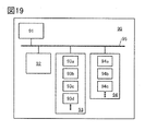
- Another aspect of the present invention is an electronic device having a housing, a display unit, and a calculation unit.
- the display unit has a first portion provided along one surface of the housing and a second portion provided along the other surface of the housing.
- the second portion has a region whose surface normal direction is different from that of the first portion.
- the second portion also has a light receiving element.
- the calculation unit has a function of executing fingerprint authentication based on a fingerprint image obtained by the light receiving element capturing the reflected light by the finger when the user's finger touches the second portion.
- a display device having a light detection function it is possible to provide a display device having a biometric authentication function represented by fingerprint authentication.
- a display device having a biometric authentication function represented by fingerprint authentication can be provided.
- a display device having both a function as a touch panel and a function of biometric authentication it is possible to provide a display device having both a function as a touch panel and a function of biometric authentication.
- a highly convenient display device can be provided.
- a multifunctional display device can be provided.
- a display device having a new configuration can be provided.
- a display device having a function of acquiring a user's health condition.
- a display device capable of managing the health of the user.
- 1A, 1B, 1D, 1F to 1H are diagrams showing a configuration example of a display device.
- 1C and 1E are diagrams showing an example of an image.
- 2A to 2C are diagrams showing a configuration example of a display device.
- 3A to 3D are diagrams showing a configuration example of a display device.
- 4A to 4C are diagrams showing a configuration example of a display device.
- 5A to 5C are diagrams showing a configuration example of a display device.
- 6A to 6C are diagrams showing a configuration example of a display device.
- 7A to 7C are diagrams showing a configuration example of a display device.
- 8A and 8B are diagrams showing a configuration example of the display device.
- FIG. 9A to 9C are diagrams showing a configuration example of the display device.
- FIG. 10 is a diagram showing a configuration example of the display device.
- FIG. 11 is a diagram showing a configuration example of the display device.
- 12A and 12B are diagrams showing a configuration example of the display device.
- 13A and 13B are diagrams showing a configuration example of the display device.
- FIG. 14 is a diagram showing a configuration example of the display device.
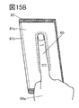
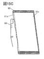
- 15A to 15C are diagrams showing a configuration example of an electronic device.
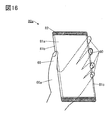
- FIG. 16 is a diagram showing a configuration example of an electronic device.
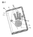
- FIG. 17 is a diagram showing a configuration example of an electronic device.
- 18A and 18B are diagrams showing a configuration example of an electronic device.
- FIG. 19 is a diagram showing a configuration example of the system.
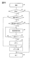
- FIG. 20 is a flowchart illustrating a method of operating the system.
- 21A and 21B are diagrams showing a configuration example of a pixel circuit.
- 22A and 22B are diagrams showing a configuration example of an electronic device.
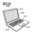
- 23A to 23D are diagrams showing a configuration example of an electronic device.
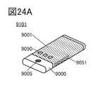
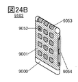
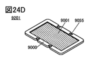
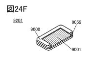
- 24A to 24F are diagrams showing configuration examples of electronic devices.
- the display panel which is one aspect of the display device, has a function of displaying (outputting) an image or the like on the display surface. Therefore, the display panel is one aspect of the output device.
- a connector such as FPC (Flexible Printed Circuit) or TCP (Tape Carrier Package) is attached to the substrate of the display panel, or an IC is used on the substrate by a COG (Chip On Glass) method or the like.
- FPC Flexible Printed Circuit
- TCP Transmission Carrier Package
- COG Chip On Glass
- the touch panel which is one aspect of the display device, has a function of displaying an image or the like on a display surface, and a touched object such as a finger or a stylus touches, presses, or approaches the display surface. It has a function as a touch sensor for detecting. Therefore, the touch panel is one aspect of the input / output device.
- the touch panel can also be called, for example, a display panel with a touch sensor (or a display device) or a display panel with a touch sensor function (or a display device).
- the touch panel may also have a configuration including a display panel and a touch sensor panel. Alternatively, it may be configured to have a function as a touch sensor inside or on the surface of the display panel.
- a touch panel board on which a connector or an IC is mounted may be referred to as a touch panel module, a display module, or simply a touch panel.
- the display device includes a display element that exhibits visible light and a light receiving element (also referred to as a light receiving device) that receives infrared light.
- the display element is preferably a light emitting element (also referred to as a first light emitting element (light emitting device)).
- the light receiving element is preferably a photoelectric conversion element.
- the display device has a substrate (also referred to as a first substrate) and a light guide plate.
- the display element and the light receiving element are arranged between the first substrate and the light guide plate.
- the display device has a light emitting element (also referred to as a second light emitting element) that emits infrared light with respect to the side surface of the light guide plate.
- Visible light emitted from the display element is emitted to the outside via the light guide plate.
- An image can be displayed by the display device having a plurality of the display elements arranged in a matrix.
- Infrared light incident from the side surface of the light guide plate diffuses inside the light guide plate while repeating total reflection.
- infrared light is scattered at the interface between the light guide plate and the object, and a part of the scattered light is scattered on the light receiving element. Be incidented.
- the light receiving element receives infrared light, it can convert it into an electric signal according to its intensity and output it.
- the display device has a plurality of light receiving elements arranged in a matrix, it is possible to detect the position information, shape, and the like of an object touching the light guide plate. That is, the display device can function as an image sensor panel, a touch sensor panel, or the like.
- infrared light that cannot be seen by the user as the light that diffuses inside the light guide plate, it is possible to perform imaging or sensing by the light receiving element without deteriorating the visibility of the displayed image. ..
- the light emitted by the second light emitting element preferably includes infrared light, preferably near infrared light.
- infrared light preferably near infrared light.
- near-infrared light having one or more peaks in the wavelength range of 700 nm or more and 2500 nm or less can be preferably used.
- the shape of the fingerprint can be captured by touching the light guide plate of the display device with the fingertip.
- the fingerprint has concave portions and convex portions, and when a finger touches the light guide plate, infrared light is likely to be scattered at the convex portions of the fingerprint that touches the light guide plate. Therefore, the intensity of the infrared light incident on the light receiving element superimposed on the convex portion of the fingerprint is large, and the intensity of the infrared light incident on the light receiving element superimposed on the concave portion is small. As a result, the fingerprint can be imaged.
- the device having the display device of one aspect of the present invention can perform fingerprint authentication, which is one of biometric authentication, by using the image of the captured fingerprint.
- the display device can also image blood vessels such as fingers and hands, especially veins.
- blood vessels such as fingers and hands, especially veins.
- light with a wavelength of 760 nm and its vicinity near infrared light
- the reflected light from the palm or finger is received by the light receiving element and imaged to form an image of the vein.
- the position can be detected.
- a device having a display device according to one aspect of the present invention can perform vein authentication, which is one of biometric authentication, by using an image of a captured vein.
- the device having the display device of one aspect of the present invention can also perform fingerprint authentication and vein authentication at the same time. As a result, biometric authentication with a higher security level can be performed without increasing the number of parts.
- the light guide plate may be flat, but part or all of it may be curved.
- the light guide plate is provided with a second portion adjacent to a portion (also referred to as a first portion) located on the main display surface and having a surface normal direction different from that of the first portion.
- the second portion is a portion located on a display surface (also referred to as a sub display surface) inclined with respect to the main display surface.
- the substrate is provided along the light guide plate. That is, the display element and the light receiving element are provided along the first portion and the second portion, respectively.
- two second portions may be provided so as to sandwich the first portion.
- a display device having a sub-display surface inclined with respect to the main display surface adjacent to the main display surface can be suitably applied to an electronic device that functions as a personal digital assistant.
- the display device it is preferable to incorporate the display device into the electronic device so that the sub-display surface is positioned at the portion where the user naturally touches the electronic device when the user holds the electronic device with one hand.
- the authentication operation by the finger touching the sub-display surface can be executed.
- the authentication is already completed and the user can be logged in, so that the user can use the electronic device immediately without waiting for authentication. It becomes possible to do.
- the light receiving element is an element capable of receiving not only infrared light but also visible light.
- the first light emitting element is made to emit light
- the reflected light reflected by the user's finger is received by the light receiving element, so that the shape of the fingerprint can be imaged.
- the shape of the vein can be imaged using infrared light. This makes it possible to perform both fingerprint authentication and vein authentication on a single display device.
- the fingerprint imaging and the vein imaging may be performed at different timings or at the same time. By simultaneously imaging the fingerprint and the vein, it is possible to acquire image data that includes both the fingerprint shape information and the vein shape information, realizing more accurate biometric authentication. it can.
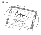
- the display device of one aspect of the present invention may have a function of detecting the health condition of the user.
- the heart rate can be determined by acquiring the time modulation of the oxygen saturation by utilizing the change in the reflectance and transmittance for visible light and infrared light according to the change in the oxygen saturation in the blood. It becomes possible to measure.
- the glucose concentration in the dermis, the triglyceride concentration in blood, and the like can also be measured by infrared light or visible light.
- the device having the display device of one aspect of the present invention can be used as a healthcare device capable of acquiring information that is an index of a user's health condition.
- a second substrate may be provided between the first substrate and the light guide plate.
- a sealing substrate for sealing the light emitting element, a protective film, or the like can be used as the second substrate.
- a resin layer for adhering these may be provided between the first substrate and the light guide plate.
- a conductive layer that transmits visible light may be provided in contact with the light guide plate.
- the infrared light can be diffused into the conductive layer, which is preferable. ..
- the conductive layer provided in contact with the light guide plate can be used, for example, as an electrostatic shielding film.
- the conductive layer can also function as, for example, an electrode of a capacitance type touch sensor.
- the conductive layer can also be used as an electrode or wiring for various sensors and functional elements.
- an EL element such as an OLED (Organic Light Emitting Diode) or a QLED (Quantum-dot Light Emitting Diode).
- the luminescent material contained in the EL element includes a substance that emits fluorescence (fluorescent material), a substance that emits phosphorescence (phosphorescent material), and a substance that exhibits thermally activated delayed fluorescence (Thermally activated delayed fluorescence: TADF) material. ), Inorganic compounds (quantum dot materials, etc.) and the like.
- an LED such as a micro LED (Light Emitting Diode) can also be used.
- the light receiving element for example, a pn type or pin type photodiode can be used.
- the light receiving element functions as a photoelectric conversion element that detects light incident on the light receiving element and generates an electric charge.
- the amount of electric charge generated is determined according to the amount of incident light.
- Organic photodiodes can be easily made thinner, lighter, and larger in area, and have a high degree of freedom in shape and design, so that they can be applied to various display devices.
- the light emitting element can have, for example, a laminated structure having a light emitting layer between a pair of electrodes. Further, the light receiving element may have a laminated structure having an active layer between the pair of electrodes.
- a semiconductor material can be used for the active layer of the light receiving element. For example, an inorganic semiconductor material such as silicon can be used.
- an organic compound for the active layer of the light receiving element.
- the other electrode of the light emitting element and the light receiving element is an electrode (also referred to as a common electrode) formed by one continuous conductive layer.
- the light emitting element and the light receiving element have a common layer.
- FIG. 1A shows a schematic view of the display device 50.
- the display device 50 includes a substrate 51, a substrate 52, a light guide plate 59, a light receiving element 53, a light emitting element 54, a light emitting element 57R, a light emitting element 57G, a light emitting element 57B, a functional layer 55, and the like.
- the light emitting element 57R, the light emitting element 57G, the light emitting element 57B, and the light receiving element 53 are provided between the substrate 51 and the substrate 52.
- the light emitting element 57R, the light emitting element 57G, and the light emitting element 57B emit red (R), green (G), or blue (B) light, respectively.
- the display device 50 has a plurality of pixels arranged in a matrix.
- One pixel has one or more sub-pixels.
- One sub-pixel has one light emitting element.
- the pixel has a configuration having three sub-pixels (three colors of R, G, B, or three colors of yellow (Y), cyan (C), and magenta (M), etc.), or sub-pixels. (4 colors of R, G, B, white (W), 4 colors of R, G, B, Y, etc.) can be applied.
- the pixel has a light receiving element 53.
- the light receiving element 53 may be provided on all pixels or may be provided on some pixels. Further, one pixel may have a plurality of light receiving elements 53.
- the light guide plate 59 is provided on the substrate 52.
- a material having high translucency with respect to visible light and infrared light For example, a material having a transmittance of 80% or more, preferably 85% or more, more preferably 90% or more, still more preferably 95% or more, and 100% or less for both light having a wavelength of 600 nm and light having a wavelength of 800 nm. Can be used.
- a material having a high refractive index for the light emitted by the light emitting element 54 for the light guide plate 59 it is preferable to use a material having a high refractive index for the light emitted by the light emitting element 54 for the light guide plate 59.
- a material having a refractive index of 1.2 or more and 2.5 or less, preferably 1.3 or more and 2.0 or less, more preferably 1.4 or more and 1.8 or less with respect to light having a wavelength of 800 nm can be used. ..
- the light guide plate 59 and the substrate 52 are provided in contact with each other, or these are bonded by a resin layer or the like. At this time, it is preferable that at least the portion of the substrate 52 or the resin layer in contact with the light guide plate 59 in contact with the light guide plate 59 has a lower refractive index for light in the wavelength range of 800 nm to 1000 nm than that of the light guide plate 59.
- the light emitting element 54 is provided near the side surface of the light guide plate 59.
- the light emitting element 54 can emit infrared light IR on the side surface of the light guide plate 59.
- a light emitting element capable of emitting infrared light including light having the above-mentioned wavelength can be used.
- an EL element such as an OLED or a QLED, or an LED can be used.
- a plurality of light emitting elements 54 may be provided along the side surface of the light guide plate 59.
- FIG. 1A shows how the finger 60 touches the surface of the light guide plate 59.
- a part of the infrared light IR diffusing inside the light guide plate 59 is reflected or scattered at the contact portion between the light guide plate 59 and the finger 60.
- a part of the scattered light IR (r) of the infrared light IR is incident on the light receiving element 53, it is possible to detect that the finger 60 has come into contact with the light guide plate 59. That is, the display device 50 can function as a touch panel.
- the functional layer 55 has a circuit for driving the light emitting element 57R, the light emitting element 57G, the light emitting element 57B, and a circuit for driving the light receiving element 53.
- the functional layer 55 is provided with a switch, a transistor, a capacitance, wiring, and the like.
- a switch or a transistor may not be provided.
- the display device 50 may have a function of detecting the fingerprint of the finger 60.
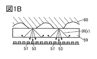
- FIG. 1B schematically shows an enlarged view of a contact portion in a state where the finger 60 is in contact with the light guide plate 59. Further, FIG. 1B shows the light emitting elements 57 and the light receiving elements 53 arranged alternately.
- Fingerprints are formed on the finger 60 by the concave and convex portions. Therefore, as shown in FIG. 1B, the convex portion of the fingerprint touches the light guide plate 59, and scattered light IR (r) is generated on these contact surfaces.
- the scattered light IR (r) scattered on the contact surface between the finger 60 and the light guide plate 59 can be isotropically scattered from the contact surface.
- the intensity distribution of the scattered light IR (r) has the highest intensity in the direction perpendicular to the contact surface, and the intensity distribution becomes lower as the angle in the oblique direction becomes larger than this. Therefore, the intensity of the light received by the light receiving element 53 located directly below the contact surface (overlapping with the contact surface) is the highest.
- the scattered light IR (r) the light having a scattering angle of a predetermined angle or more is totally reflected by the other surface (the surface opposite to the contact surface) of the light guide plate 59 as shown in FIG. 1B. , It does not pass through to the light receiving element 53 side.
- a clear fingerprint image can be obtained by setting the arrangement interval of the light receiving element 53 to be smaller than the distance between the two convex portions of the fingerprint, preferably the distance between the adjacent concave portion and the convex portion. Since the distance between the concave portion and the convex portion of the human fingerprint is approximately 200 ⁇ m, for example, the arrangement distance of the light receiving element 53 is 400 ⁇ m or less, preferably 200 ⁇ m or less, more preferably 150 ⁇ m or less, still more preferably 100 ⁇ m or less, still more preferably. It is 50 ⁇ m or less, 1 ⁇ m or more, preferably 10 ⁇ m or more, and more preferably 20 ⁇ m or more.
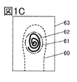
- FIG. 1C shows an example of a fingerprint image captured by the display device 50.
- the contour of the finger 60 is shown by a broken line and the contour of the contact portion 61 is shown by a chain line within the imaging range 63.
- a high-contrast fingerprint 62 can be imaged in the contact portion 61 due to the difference in the amount of light incident on the light receiving element 53.
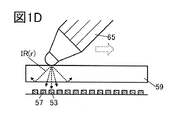
- the display device 50 can also function as a touch panel or a pen tablet.
- FIG. 1D shows a state in which the tip of the stylus 65 is in contact with the light guide plate 59 and is slid in the direction of the broken line arrow.
- the scattered light IR (r) scattered on the contact surface between the tip of the stylus 65 and the light guide plate 59 is incident on the light receiving element 53 located at the portion overlapping the scattering surface, thereby causing the stylus.
- the position of the tip of 65 can be detected with high accuracy.
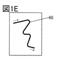
- FIG. 1E shows an example of the locus 66 of the stylus 65 detected by the display device 50. Since the display device 50 can detect the position of the object to be detected such as the stylus 65 with high position accuracy, it is also possible to perform high-definition drawing in a drawing application or the like.
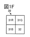
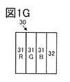
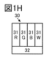
- FIGS. 1F to 1H show an example of pixels 30 applicable to the display device 50.
- the pixels 30 shown in FIGS. 1F and 1G are a red (R) pixel 31R, a green (G) pixel 31G, a blue (B) pixel 31B, and a light receiving pixel, which function as sub-pixels for display, respectively. It has a pixel 32 that functions as.
- Each of the pixel 31R, the pixel 31G, and the pixel 31B has one or more light emitting elements 57R, a light emitting element 57G, or a light emitting element 57B, respectively.
- the pixel 32 has one or more light receiving elements 53.
- FIG. 1F is an example in which three sub-pixels and pixels 32 are arranged in a 2 ⁇ 2 matrix.
- FIG. 1G is an example in which three sub-pixels and pixels 32 are arranged in a row.
- the pixel 30 shown in FIG. 1H is an example having a white (W) pixel 31W.
- the pixel 31W has one or more white light emitting elements.
- four sub-pixels are arranged in a horizontal row, and pixels 32 are arranged below the four sub-pixels.
- the pixel configuration is not limited to the above, and various arrangement methods can be adopted.
- the display device uses both visible light and infrared light to capture both fingerprints and blood vessels, a mode in which fingerprints are imaged using visible light, a mode in which blood vessels are imaged using infrared light, and a mode in which both visible light and infrared light are used.
- a mode of capturing as one image and a mode can be executed.
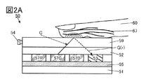
- FIG. 2A shows a state in which a fingerprint is imaged using visible light.
- the light emitting element 54 is not made to emit light, but the light emitting element 57G is made to emit light.
- the green light G emitted by the light emitting element 57G irradiates the surface of the finger 60, and a part thereof is reflected or scattered. Then, a part of the scattered light G (r) is incident on the light receiving element 53. Since the light receiving elements 53 are arranged in a matrix, an image of the fingerprint of the finger 60 can be acquired by mapping the intensity of the scattered light G (r) detected by each light receiving element 53.
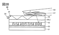
- FIG. 2B shows a state in which blood vessels are imaged using infrared light.
- the light emitting element 57R, the light emitting element 57G, and the light emitting element 57B are not made to emit light, but the light emitting element 54 is made to emit light.
- a part of the infrared light IR diffusing inside the light guide plate 59 is transmitted from the contact portion between the light guide plate 59 and the finger 60 to the inside of the finger 60.
- a part of the infrared light IR is reflected or scattered by the blood vessel 67 located inside the finger 60, and the reflected light IR (r) is incident on the light receiving element 53.
- mapping the intensity of the incident light IR (r) in the same manner as described above, an image of the blood vessel 67 can be acquired.
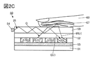
- FIG. 2C shows a state in which imaging using visible light and imaging using infrared light are performed at the same time.
- Scattered light G (r) and scattered light IR (r) are incident on the light receiving element 53.
- the blood vessel 67 includes a vein and an artery.
- the image can be used for vein authentication.
- the reflectance of the arteries (arterioles) inside the finger 60 to infrared light or visible light changes according to the fluctuation of blood oxygen saturation.
- pulse wave information can be acquired. This makes it possible to measure the user's heart rate.
- infrared light IR is shown here, it can also be measured using visible light.
- the information obtained by imaging the inside of the finger 60 and the blood vessel 67 includes the neutral fat concentration in blood and the glucose concentration in blood or dermis. ..
- the blood glucose level can be estimated from the glucose concentration. Since such information serves as an index of the user's health condition, it is possible to monitor changes in the daily health condition by measuring the information at least once a day. Since the device having the display device of one aspect of the present invention can acquire biometric information at the same time when performing fingerprint authentication or vein authentication, it is possible to unconsciously perform health management without bothering the user. Can be done.
- the light emitting element 57G that emits green light is used as the light source of visible light, but the present invention is not limited to this, and the light emitting element 57R or the light emitting element 57B may be used, or 2 out of 3 light emitting elements. One or more may be used. Further, as the light emitting element 54, not only one type of light emitting element may be used, but also a plurality of light emitting elements that emit infrared light having different wavelengths may be used, or a light emitting element that emits infrared light having a continuous wavelength may be used. You may. As the light source used for fingerprint authentication, vein authentication, or acquisition of biometric information, a light source that emits light having a suitable wavelength can be selected and used according to the application.
- Display device configuration example 2 Hereinafter, a configuration example of a display device having a partially different configuration from the above will be described.
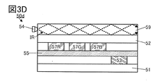
- the display device 50a shown in FIG. 3A is mainly different from the display device 50 in that it has a resin layer 71 instead of the substrate 52.
- the resin layer 71 a material having translucency with respect to visible light can be used. Further, the resin layer 71 may have a function of adhering the substrate 51 and the light guide plate 59.
- the resin layer 71 is provided in contact with the light guide plate 59.
- the resin layer 71 has a lower refractive index with respect to light in the wavelength range of 800 nm to 1000 nm than that of the light guide plate 59, at least in a portion in contact with the light guide plate 59.
- the infrared light IR can be totally reflected at the interface between the light guide plate 59 and the resin layer 71.
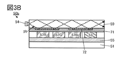
- the display device 50b shown in FIG. 3B is mainly different from the display device 50a in that it has a conductive layer 72.
- the conductive layer 72 is provided in contact with the light guide plate 59.
- an example is shown in which the conductive layer 72 is located between the light guide plate 59 and the resin layer 71.
- the conductive layer 72 By applying a predetermined potential to the conductive layer 72, it can function as an electrostatic shielding film.
- the conductive layer 72 can suitably prevent electrical noise input from the outside via the light guide plate 59 from reaching the circuit or the like of the display device 50b.
- the conductive layer 72 can also function as an electrode of a sensor element such as a touch sensor. In particular, it is preferable to use it as an electrode of a capacitance type touch sensor.
- a conductive material that transmits visible light can be used.
- a conductive material that transmits infrared light IR emitted by the light emitting element 54 can be preferably used for the conductive layer 72.
- the conductive layer 72 it is preferable to use a conductive material having a higher refractive index for light in the wavelength range of 800 nm to 1000 nm than the light guide plate 59, at least in a portion in contact with the light guide plate 59.
- the infrared light IR can be diffused not only inside the light guide plate 59 but also inside the conductive layer 72.
- the conductive layer 72 has a higher refractive index with respect to light in the above-mentioned wavelength range than the resin layer 71, infrared light IR can be totally reflected at the interface between the conductive layer 72 and the resin layer 71.
- the configuration may have the substrate 52.
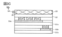
- the display device 50c shown in FIG. 3C shows an example in which the light emitting element 57R and the like and the light receiving element 53 are provided on different surfaces.
- the display device 50c includes a substrate 51a, a substrate 51b, a functional layer 55a, a functional layer 55b, and the like.
- the functional layer 55a is a layer having a circuit for driving the light emitting element 57R and the like, and is provided on the substrate 51a. Further, the functional layer 55b is a layer having a circuit for driving the light receiving element 53, and is provided on the substrate 51b. It is preferable that the substrate 51a and the substrate 51b are fixed by an adhesive layer or the like (not shown).
- an inorganic semiconductor material such as silicon can be used for the active layer of the light receiving element 53.
- the active layer single crystal silicon, polycrystalline silicon, amorphous silicon, or the like can be selected and used according to the wavelength of infrared light IR.
- the substrate 51b is the functional layer 55b and the light receiving element 53. It may form a part.
- the display device 50d shown in FIG. 3D is mainly different from the display device 50c in that the light emitting element 57R and the like and the light receiving element 53 are provided with the functional layer 55 interposed therebetween.
- the above-mentioned inorganic semiconductor material such as silicon can be used for the active layer of the light receiving element 53. Further, when a semiconductor substrate is used as the substrate 51, the substrate 51 may form a part of the active layer of the light receiving element 53 or the like.
- the display device 50c and the display device 50d may be configured to have a resin layer 71 instead of the substrate 52, or may have a configuration having a conductive layer 72.
- the light guide plate applicable to the display device of one aspect of the present invention is provided on, for example, a display unit of an electronic device, and can also serve as a part of a housing that functions as a display surface or a touch surface.
- the light guide plate also functions as a protective member that protects the light emitting element, the light receiving element, the functional layer, and the like.
- tempered glass, a flexible film, or the like can be used as the light guide plate.
- FIG. 4A shows a configuration example of the display device 50e.
- the display device 50e has a configuration in which a light guide plate 59a is provided on the substrate 52.
- FIG. 4A is an example of having a flat plate-shaped light guide plate 59a.
- a light emitting element 54 that emits infrared light IR is arranged along one end. Further, a reflective layer 58 is provided on the side of the light guide plate 59a opposite to the side on which the light emitting element 54 is provided. The reflective layer 58 has a function of reflecting infrared light IR. By providing the reflective layer 58, the intensity distribution of the infrared light IR diffused in the light guide plate 59a can be made uniform.
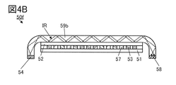
- FIG. 4B shows a configuration example of a display device 50f having a light guide plate 59b with curved ends.
- the light guide plate 59b is provided with a light emitting element 54 along one end and a reflection layer 58 along the other end. Infrared light IR is diffused inside the light guide plate 59b.
- a non-display area (also referred to as a frame) surrounding the display unit in the electronic device to which the display device 50f is applied is provided. ) Can be reduced, which is preferable.
- the thickness of the light guide plate 59b is 2 mm or less, preferably 1 mm or less, more preferably 0.8 mm or less, further preferably 0.7 mm or less, and 10 ⁇ m or more, preferably 30 ⁇ m or more, more preferably 50 ⁇ m or more. By doing so, it is possible to suppress a decrease in the intensity of the infrared light IR in the light guide plate 59b.
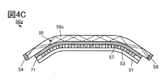
- FIG. 4C shows a configuration example of the display device 50 g in which the substrate 51 and the like are provided in a curved manner along the light guide plate 59c which is partially curved.
- a flexible material can be used for the substrate 51.
- an inorganic insulating substrate such as a glass substrate can be used as the substrate 51.
- a material containing an organic resin or the like is preferable to use as the substrate 51.
- FIG. 4C shows an example in which the substrate 51 and the light guide plate 59c are bonded by the resin layer 71.
- the substrate 51 and the light guide plate 59c can be easily bonded to each other. It is preferable because it can be used.
- the distance between the light receiving element 53 and the light guide plate 59c can be shortened, the accuracy of position detection is improved and a clear image can be taken.
- FIG. 4C shows an example in which the light guide plate 59c has a curved portion and a flat portion
- the light guide plate 59c may have a curved shape as a whole without having a flat portion.
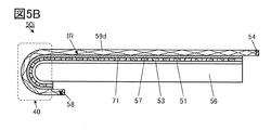
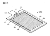
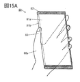
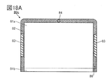
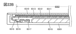
- FIG. 5A shows a configuration example of a display device 50h in which the light guide plate 59d has a shape curved by 180 degrees at an end portion.
- the display device 50h has a curved portion 40.
- the portion of the display device 50h other than the curved portion 40 can be called a first display unit that functions as a main display surface. Further, the curved portion 40 can be called a second display portion that functions as a sub-display surface.
- the area of the second display unit is smaller than that of the first display unit.
- the surface of the light guide plate 59d that functions as the main display surface (first surface) is larger than the area of the surface (second surface) that is located at the curved portion 40 and functions as the sub display surface. It is preferable that the area is small.
- an image can be displayed along a curved surface by a light emitting element 57 provided between the light guide plate 59d and the substrate 51. Further, the light receiving element 53 provided on the curved portion 40 can receive infrared light IR, visible light, and the like reflected from the object to be detected that touches the curved portion 40.
- the light guide plate 59d has a first portion having a first surface located on the first display unit, and a second portion which is continuous with the first surface and whose normal direction is different from that of the first surface. It can also be said to have a second portion having two faces. The second portion is located on the second display unit. Further, it can be said that the substrate 51 has a third portion provided along the first portion of the light guide plate 59d and a fourth portion provided along the second portion of the light guide plate 59d.
- the surface of the light guide plate 59d located on the first display portion is preferably a flat surface.
- the surface may have a curved surface portion having a curvature smaller than that of the curved portion 40.
- FIG. 5A shows an example in which the substrate 51 is supported by the support member 56.
- the support member 56 a part of the housing of the electronic device incorporating the display device 50h can be applied.
- the mechanical strength can be increased.
- the light emitting element 54 is arranged at the end of the light guide plate 59d on the curved portion 40 side. As a result, the light emitting element 54 can be arranged on the back side of the support member 56. Therefore, the frame surrounding the display unit in the electronic device to which the display device 50h is applied can be reduced, and the design of the electronic device can be enhanced.
- FIG. 5A shows an example in which the light guide plate 59d, the substrate 51, and the like are curved by 180 degrees in the curved portion 40, but the present invention is not limited to this.
- it can be configured to be curved at an angle of 30 degrees or more and 180 degrees or less, preferably 60 degrees or more and 180 degrees or less, and more preferably 90 degrees or more and 180 degrees or less.
- the display device 50i shown in FIG. 5B is an example in which the light emitting element 54 is arranged on the opposite side of the curved portion 40.
- a reflection layer 58 is provided at the end of the light guide plate 59d on the curved portion 40 side.
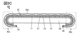
- the display device 50j shown in FIG. 5C has a pair of curved portions 40a and a curved portion 40b.
- the light guide plate 59e has a pair of curved portions located on the second display portion with a portion located on the first display portion interposed therebetween.
- both ends of the light guide plate 59e can be folded back to the side opposite to the main display surface, so that the frame in the electronic device to which the display device 50j is applied can be substantially eliminated. As a result, it is possible to realize an electronic device having excellent design and convenience.
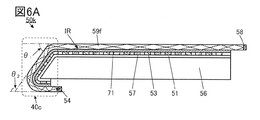
- the display device 50k shown in FIG. 6A is an example in which the curved portion 40c functioning as the second display portion has a flat surface.
- the light guide plate 59f has a portion located on the first display portion and a portion located on the curved portion 40c functioning as the second display portion.
- the flat portion of the light guide plate 59f located at the curved portion 40c is provided so as to be sandwiched between the pair of curved portions. That is, a curved portion is provided between the portion of the light guide plate 59f located at the first display portion and the flat portion located at the curved portion 40c.
- the display device 50k shown in FIG. 6A has a first display unit that functions as a main display surface and a second display unit that is inclined with respect to the first display unit.
- the contact area when the finger touches the curved portion 40c can be increased, so that more accurate authentication can be performed.
- the angle (angle ⁇ 1 ) formed by the surface of the light guide plate 59f located on the first display portion and the surface of the flat portion located on the curved portion 40c is greater than 0 degrees and 90 degrees or less. Is preferable. Specifically, it can be 15 degrees or more and 90 degrees or less, preferably 20 degrees or more and less than 90 degrees, and more preferably 25 degrees or more and 90 degrees or less. Typically, the angle ⁇ 1 can be 30 degrees, 45 degrees, 60 degrees, 75 degrees, or the like.
- the angle (angle ⁇ 2 ) formed by the surface of the flat portion of the light guide plate 59f located at the curved portion 40c and the surface of the flat portion near the light emitting element 54 is an angle obtained by subtracting the above angle ⁇ 1 from 180 degrees. Is preferable.
- the area of the second display unit is smaller than that of the first display unit.
- the surface (second surface) of the light guide plate 59f that is located at the curved portion 40c and functions as the sub-display surface is larger than the area of the surface (first surface) that functions as the main display surface. It is preferable that the area is small.
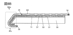
- FIG. 6A shows an example in which the light emitting element 54 is arranged on the curved portion 40c side of the light guide plate 59f, but is arranged on the side opposite to the curved portion 40c of the light guide plate 59f as in the display device 50m shown in FIG. 6B. You may. At this time, the reflective layer 58 can be provided on the curved portion 40c side of the light guide plate 59f.
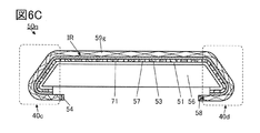
- the display device 50n shown in FIG. 6C has a pair of curved portions 40c and curved portions 40d.
- both ends of the light guide plate 59g of the display device 50n can be folded back to the side opposite to the main display surface, so that the frame in the electronic device to which the display device 50n is applied can be substantially. Can be eliminated. As a result, it is possible to realize an electronic device having excellent design and convenience.
- Display device configuration example 3 Hereinafter, a more specific example of the display device according to one aspect of the present invention will be described.
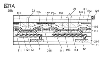
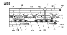
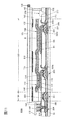
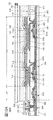
- FIG. 7A shows a schematic cross-sectional view of the display device 10A.
- the display device 10A has a light receiving element 110 and a light emitting element 190.
- the light receiving element 110 has a pixel electrode 111, a common layer 112, an active layer 113, a common layer 114, and a common electrode 115.
- the light emitting element 190 has a pixel electrode 191 and a common layer 112, a light emitting layer 193, a common layer 114, and a common electrode 115.
- the pixel electrode 111, the pixel electrode 191 and the common layer 112, the active layer 113, the light emitting layer 193, the common layer 114, and the common electrode 115 may each have a single layer structure or a laminated structure.
- the pixel electrode 111 and the pixel electrode 191 are located on the insulating layer 214.
- the pixel electrode 111 and the pixel electrode 191 can be formed of the same material and in the same process.
- the common layer 112 is located on the pixel electrode 111 and on the pixel electrode 191.
- the common layer 112 is a layer commonly used for the light receiving element 110 and the light emitting element 190.
- the active layer 113 overlaps with the pixel electrode 111 via the common layer 112.
- the light emitting layer 193 overlaps with the pixel electrode 191 via the common layer 112.
- the active layer 113 has a first organic compound, and the light emitting layer 193 has a second organic compound different from the first organic compound.
- the common layer 114 is located on the common layer 112, the active layer 113, and the light emitting layer 193.
- the common layer 114 is a layer commonly used for the light receiving element 110 and the light emitting element 190.
- the common electrode 115 has a portion that overlaps with the pixel electrode 111 via the common layer 112, the active layer 113, and the common layer 114. Further, the common electrode 115 has a portion that overlaps with the pixel electrode 191 via the common layer 112, the light emitting layer 193, and the common layer 114.
- the common electrode 115 is a layer commonly used for the light receiving element 110 and the light emitting element 190.
- an organic compound is used for the active layer 113 of the light receiving element 110.
- the light receiving element 110 can have a layer other than the active layer 113 having the same configuration as the light emitting element 190 (EL element). Therefore, the light receiving element 110 can be formed in parallel with the formation of the light emitting element 190 only by adding the step of forming the active layer 113 to the manufacturing process of the light emitting element 190. Further, the light emitting element 190 and the light receiving element 110 can be formed on the same substrate. Therefore, the light receiving element 110 can be built in the display device without significantly increasing the manufacturing process.
- the display device 10A shows an example in which the light receiving element 110 and the light emitting element 190 have a common configuration except that the active layer 113 of the light receiving element 110 and the light emitting layer 193 of the light emitting element 190 are separately formed.
- the configuration of the light receiving element 110 and the light emitting element 190 is not limited to this.
- the light receiving element 110 and the light emitting element 190 may have layers that are separated from each other (see display devices 10D, 10E, and 10F described later).
- the light receiving element 110 and the light emitting element 190 preferably have one or more layers (common layers) that are commonly used. As a result, the light receiving element 110 can be incorporated in the display device without significantly increasing the manufacturing process.
- the display device 10A has a light receiving element 110, a light emitting element 190, a transistor 41, a transistor 42, and the like between a pair of substrates (board 151 and substrate 152).
- the display device 10A has a light guide plate 121 on the outside of the substrate 152.
- a light emitting element 122 that emits infrared light is arranged at the end of the light guide plate 121.
- the common layer 112, the active layer 113, and the common layer 114 located between the pixel electrode 111 and the common electrode 115 can also be referred to as an organic layer (a layer containing an organic compound).
- the pixel electrode 111 preferably has a function of reflecting visible light and infrared light.
- the end of the pixel electrode 111 is covered with a partition wall 216.
- the common electrode 115 has a function of transmitting visible light and infrared light.
- the light receiving element 110 has a function of detecting light. Specifically, the light receiving element 110 is a photoelectric conversion element that receives light 22 incident from the light guide plate 121 and converts it into an electric signal.
- a light-shielding layer BM is provided on the surface of the substrate 152 on the substrate 151 side.
- the light-shielding layer BM has openings at a position where it overlaps with the light receiving element 110 and a position where it overlaps with the light emitting element 190.
- the light-shielding layer BM a material that blocks light emission from the light-emitting element can be used.
- the light-shielding layer BM preferably absorbs visible light.
- a metal material or a resin material containing a pigment (carbon black or the like) or a dye can be used to form a black matrix.
- the light-shielding layer BM may have a laminated structure of a red color filter, a green color filter, and a blue color filter.
- the light receiving element 110 detects the light scattered on the surface of the light guide plate 121.
- the light emitted from the light emitting element 190 may be reflected in the display device 10A and may be incident on the light receiving element 110 without passing through the light guide plate 121 or the like.
- the light-shielding layer BM can suppress the influence of such stray light.
- the light-shielding layer BM is not provided, the light 23a emitted by the light emitting element 190 may be reflected by the substrate 152, and the reflected light 23b may be incident on the light receiving element 110.
- the light-shielding layer BM it is possible to prevent the reflected light 23b from being incident on the light receiving element 110. As a result, noise can be reduced and the sensitivity of the sensor using the light receiving element 110 can be increased.
- the common layer 112, the light emitting layer 193, and the common layer 114 located between the pixel electrode 191 and the common electrode 115 can also be said to be EL layers.
- the pixel electrode 191 preferably has a function of reflecting visible light and infrared light.
- the end of the pixel electrode 191 is covered with a partition wall 216.
- the pixel electrode 111 and the pixel electrode 191 are electrically insulated from each other by a partition wall 216.
- the common electrode 115 has a function of transmitting visible light and infrared light.
- the light emitting element 190 has a function of emitting visible light.
- the light emitting element 190 is an electroluminescent element that emits light 21 toward the substrate 152 by applying a voltage between the pixel electrode 191 and the common electrode 115.
- the light emitting layer 193 is preferably formed so as not to overlap the light receiving region of the light receiving element 110. As a result, it is possible to suppress the light emitting layer 193 from absorbing the light 22, and it is possible to increase the amount of light emitted to the light receiving element 110.
- the pixel electrode 111 is electrically connected to the source or drain of the transistor 41 through an opening provided in the insulating layer 214.
- the end of the pixel electrode 111 is covered with a partition wall 216.
- the pixel electrode 191 is electrically connected to the source or drain of the transistor 42 through an opening provided in the insulating layer 214.
- the end of the pixel electrode 191 is covered with a partition wall 216.
- the transistor 42 has a function of controlling the drive of the light emitting element 190.
- the transistor 41 and the transistor 42 are in contact with the upper surface of the same layer (the substrate 151 in FIG. 7A).
- At least a part of the circuit electrically connected to the light receiving element 110 is formed of the same material and the same process as the circuit electrically connected to the light emitting element 190.
- the thickness of the display device can be reduced and the manufacturing process can be simplified as compared with the case where the two circuits are formed separately.
- the light receiving element 110 and the light emitting element 190 are each covered with a protective layer 195.
- the protective layer 195 is provided in contact with the common electrode 115.
- impurities such as water can be suppressed from entering the light receiving element 110 and the light emitting element 190, and the reliability of the light receiving element 110 and the light emitting element 190 can be improved.
- the protective layer 195 and the substrate 152 are bonded to each other by the adhesive layer 142.
- the common electrode 115 and the substrate 152 are bonded to each other by the adhesive layer 142.
- the configuration may not have the light-shielding layer BM.
- the light receiving area of the light receiving element 110 can be increased, so that the sensitivity of the sensor can be further increased.
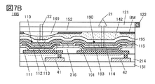
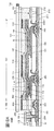
- FIG. 7B shows a cross-sectional view of the display device 10B.
- the description of the same configuration as the display device described above may be omitted.
- the display device 10B shown in FIG. 7B has a lens 149 in addition to the configuration of the display device 10A.
- the lens 149 is provided at a position where it overlaps with the light receiving element 110.
- the lens 149 is provided in contact with the substrate 152.
- the lens 149 included in the display device 10B is a convex lens having a convex surface on the substrate 151 side.
- a convex lens having a convex surface on the substrate 152 side may be arranged at a position overlapping the light receiving element 110.
- FIG. 7B shows an example in which the lens 149 is formed first, the light-shielding layer BM may be formed first. In FIG. 7B, the end of the lens 149 is covered with a light-shielding layer BM.
- the display device 10B has a configuration in which the light 22 is incident on the light receiving element 110 via the lens 149.
- the imaging range of the light receiving element 110 can be narrowed as compared with the case where the lens 149 is not provided, and the overlapping of the imaging range with the adjacent light receiving element 110 can be suppressed. As a result, a clear image with less blur can be captured.
- the size of the pinhole in FIG. 7B, the size of the opening of the BM overlapping the light receiving element 110
- the lens 149 is provided, the size of the pinhole (in FIG. 7B, the size of the opening of the BM overlapping the light receiving element 110) is larger than that when the lens 149 is not provided. (Equivalent) can be increased. Therefore, by having the lens 149, the amount of light incident on the light receiving element 110 can be increased.
- a lens such as a microlens may be directly formed on a substrate or a light receiving element, or a separately manufactured lens array such as a microlens array may be formed on the substrate. It may be pasted on.
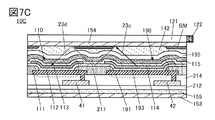
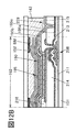
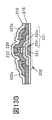
- FIG. 7C shows a schematic cross-sectional view of the display device 10C.
- the display device 10C differs from the display device 10A in that it does not have a substrate 151, a substrate 152, and a partition wall 216, and has a substrate 153, a substrate 154, an adhesive layer 155, an insulating layer 212, and a partition wall 217.
- the substrate 153 and the insulating layer 212 are bonded to each other by the adhesive layer 155.
- the substrate 154 and the protective layer 195 are bonded to each other by an adhesive layer 142.
- the display device 10C has a configuration in which the insulating layer 212, the transistor 41, the transistor 42, the light receiving element 110, the light emitting element 190, and the like formed on the manufactured substrate are transposed on the substrate 153. It is preferable that the substrate 153 and the substrate 154 each have flexibility. Thereby, the flexibility of the display device 10C can be increased. For example, it is preferable to use a resin for the substrate 153 and the substrate 154, respectively.
- the substrates 153 and 154 include polyester resins such as polyethylene terephthalate (PET) and polyethylene naphthalate (PEN), polyacrylonitrile resins, acrylic resins, polyimide resins, polymethyl methacrylate resins, polycarbonate (PC) resins, and polyethers, respectively.
- polyester resins such as polyethylene terephthalate (PET) and polyethylene naphthalate (PEN), polyacrylonitrile resins, acrylic resins, polyimide resins, polymethyl methacrylate resins, polycarbonate (PC) resins, and polyethers, respectively.
- Sulfonate (PES) resin polyamide resin (nylon, aramid, etc.), polysiloxane resin, cycloolefin resin, polystyrene resin, polyamideimide resin, polyurethane resin, polyvinyl chloride resin, polyvinylidene chloride resin, polypropylene resin, polytetrafluoroethylene (PTFE) resin, ABS resin, cellulose nanofibers and the like can be used.
- PES Sulfonate
- polyamide resin nylon, aramid, etc.
- polysiloxane resin cycloolefin resin
- polystyrene resin polyamideimide resin
- polyurethane resin polyvinyl chloride resin
- polyvinylidene chloride resin polypropylene resin
- PTFE polytetrafluoroethylene
- ABS resin cellulose nanofibers and the like
- a film having high optical isotropic properties may be used for the substrate included in the display device of the present embodiment.
- the film having high optical isotropic properties include a triacetyl cellulose (TAC, also referred to as cellulose triacetate) film, a cycloolefin polymer (COP) film, a cycloolefin copolymer (COC) film, and an acrylic film.
- TAC triacetyl cellulose
- COP cycloolefin polymer
- COC cycloolefin copolymer
- the partition wall 217 preferably absorbs the light emitted by the light emitting element.
- a black matrix can be formed by using a resin material containing a pigment or a dye. Further, by using a brown resist material, the partition wall 217 can be formed of a colored insulating layer.
- the light 23c emitted by the light emitting element 190 is reflected by the substrate 154 and the partition wall 217, and the reflected light 23d is incident on the light receiving element 110. There is. Further, the light 23c passes through the partition wall 217 and is reflected by a transistor, wiring, or the like, so that the reflected light may be incident on the light receiving element 110. By absorbing the light 23c by the partition wall 217, it is possible to suppress the reflected light 23d from entering the light receiving element 110. As a result, noise can be reduced and the sensitivity of the sensor using the light receiving element 110 can be increased.
- the partition wall 217 preferably absorbs at least the wavelength of light detected by the light receiving element 110.
- the partition wall 217 preferably absorbs at least the red light.
- the partition wall 217 has a blue color filter, the red light 23c can be absorbed and the reflected light 23d can be suppressed from being incident on the light receiving element 110.
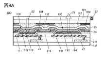
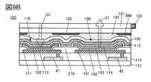
- FIG. 9A shows a schematic cross-sectional view of the display device 10D.
- the display device 10D differs from the display device 10A in that it does not have a common layer 114 and has a buffer layer 184 and a buffer layer 194.
- the buffer layer 184 and the buffer layer 194 may have a single-layer structure or a laminated structure, respectively.
- the light receiving element 110 has a pixel electrode 111, a common layer 112, an active layer 113, a buffer layer 184, and a common electrode 115.
- the light emitting element 190 has a pixel electrode 191 and a common layer 112, a light emitting layer 193, a buffer layer 194, and a common electrode 115.
- the buffer layer 184 between the common electrode 115 and the active layer 113 and the buffer layer 194 between the common electrode 115 and the light emitting layer 193 are separately formed.
- the buffer layer 184 and the buffer layer 194 for example, one or both of the electron injection layer and the electron transport layer can be formed.
- FIG. 9B shows a schematic cross-sectional view of the display device 10E.
- the display device 10E differs from the display device 10A in that it does not have the common layer 112 and has the buffer layer 182 and the buffer layer 192.
- the buffer layer 182 and the buffer layer 192 may have a single-layer structure or a laminated structure, respectively.
- the light receiving element 110 has a pixel electrode 111, a buffer layer 182, an active layer 113, a common layer 114, and a common electrode 115.
- the light emitting element 190 has a pixel electrode 191 and a buffer layer 192, a light emitting layer 193, a common layer 114, and a common electrode 115.
- the display device 10E shows an example in which the buffer layer 182 between the pixel electrode 111 and the active layer 113 and the buffer layer 192 between the pixel electrode 191 and the light emitting layer 193 are separately formed.
- the buffer layer 182 and the buffer layer 192 for example, one or both of the hole injection layer and the hole transport layer can be formed.
- FIG. 9C shows a schematic cross-sectional view of the display device 10F.
- the display device 10F differs from the display device 10A in that it does not have the common layer 112 and the common layer 114 and has the buffer layer 182, the buffer layer 184, the buffer layer 192, and the buffer layer 194.
- the light receiving element 110 has a pixel electrode 111, a buffer layer 182, an active layer 113, a buffer layer 184, and a common electrode 115.
- the light emitting element 190 has a pixel electrode 191 and a buffer layer 192, a light emitting layer 193, a buffer layer 194, and a common electrode 115.
- the active layer 113 and the light emitting layer 193 can be produced separately, but also other layers can be produced separately.
- the light receiving element 110 and the light emitting element 190 do not have a common layer between a pair of electrodes (pixel electrode 111 or pixel electrode 191 and common electrode 115).
- the pixel electrode 111 and the pixel electrode 191 are formed on the insulating layer 214 by the same material and the same process, and the buffer layer 182 and the active layer are formed on the pixel electrode 111.
- the common electrode 115 is formed so as to cover the buffer layer 184, the buffer layer 194, and the like. It can be made by.
- the order of producing the laminated structure of the buffer layer 182, the active layer 113, and the buffer layer 184 and the laminated structure of the buffer layer 192, the light emitting layer 193, and the buffer layer 194 is not particularly limited.
- the buffer layer 192, the light emitting layer 193, and the buffer layer 194 may be formed after the buffer layer 182, the active layer 113, and the buffer layer 184 are formed.
- the buffer layer 192, the light emitting layer 193, and the buffer layer 194 may be formed before the buffer layer 182, the active layer 113, and the buffer layer 184 are formed.
- the buffer layer 182, the buffer layer 192, the active layer 113, the light emitting layer 193, and the like may be alternately formed in this order.
- Display device configuration example 4 Hereinafter, a more specific configuration example of the display device according to one aspect of the present invention will be described.
- FIG. 10 shows a perspective view of the display device 100A.
- the display device 100A has a configuration in which the substrate 151 and the substrate 152 are bonded together. Further, a light guide plate 121 is provided on the substrate 152. In FIG. 10, the substrate 152 and the light guide plate 121 are shown by broken lines.
- the display device 100A has a display unit 162, a circuit 164, wiring 165, and the like.
- FIG. 10 shows an example in which an IC (integrated circuit) 173 and an FPC 172 are mounted on the display device 100A. Therefore, the configuration shown in FIG. 10 can be said to be a display module having a display device 100A, IC173, and FPC172.
- a scanning line drive circuit can be used as the circuit 164.
- the wiring 165 has a function of supplying signals and electric power to the display unit 162 and the circuit 164.
- the signal and power are input from the outside via FPC172 or input from IC173 to wiring 165.
- FIG. 10 shows an example in which the IC173 is provided on the substrate 151 by the COG (Chip On Glass) method, the COF (Chip On Film) method, or the like.
- the IC 173 for example, an IC having a scanning line drive circuit, a signal line drive circuit, or the like can be applied.
- the display device 100A and the display module may be configured without an IC. Further, the IC may be mounted on the FPC172 by the COF method or the like.
- FIG. 11 shows a part of the area including the FPC 172, a part of the area including the circuit 164, a part of the area including the display unit 162, and one of the areas including the end of the display device 100A shown in FIG. An example of the cross section when each part is cut is shown.
- the display device 100A shown in FIG. 11 has a transistor 201, a transistor 205, a transistor 206, a light emitting element 190, a light receiving element 110, and the like between the substrate 151 and the substrate 152.
- a light guide plate 121 is provided on the substrate 152.
- a light emitting element 122 is provided at the end of the light guide plate 121.
- the substrate 152 and the insulating layer 214 are adhered to each other via the adhesive layer 142.
- a solid sealing structure, a hollow sealing structure, or the like can be applied to seal the light emitting element 190 and the light receiving element 110.
- the space 143 surrounded by the substrate 152, the adhesive layer 142, and the insulating layer 214 is filled with an inert gas (nitrogen, argon, etc.), and a hollow sealing structure is applied.
- the adhesive layer 142 may be provided so as to overlap with the light emitting element 190.
- the space 143 surrounded by the substrate 152, the adhesive layer 142, and the insulating layer 214 may be filled with a resin different from that of the adhesive layer 142.
- the light emitting element 190 has a laminated structure in which the pixel electrode 191 and the common layer 112, the light emitting layer 193, the common layer 114, and the common electrode 115 are laminated in this order from the insulating layer 214 side.
- the pixel electrode 191 is connected to the conductive layer 222b of the transistor 206 via an opening provided in the insulating layer 214.
- the transistor 206 has a function of controlling the drive of the light emitting element 190.
- the end of the pixel electrode 191 is covered with a partition wall 216.
- the pixel electrode 191 contains a material that reflects visible light and infrared light
- the common electrode 115 contains a material that transmits visible light and infrared light.
- the light receiving element 110 has a laminated structure in which the pixel electrode 111, the common layer 112, the active layer 113, the common layer 114, and the common electrode 115 are laminated in this order from the insulating layer 214 side.
- the pixel electrode 111 is electrically connected to the conductive layer 222b of the transistor 205 via an opening provided in the insulating layer 214.
- the end of the pixel electrode 111 is covered with a partition wall 216.
- the pixel electrode 111 contains a material that reflects visible light and infrared light
- the common electrode 115 contains a material that transmits visible light and infrared light.
- the light emitted by the light emitting element 190 is emitted to the substrate 152 side. Further, light is incident on the light receiving element 110 via the substrate 152 and the space 143. It is preferable to use a material having high transparency to visible light and infrared light for the substrate 152.
- the pixel electrode 111 and the pixel electrode 191 can be manufactured by the same material and the same process.
- the common layer 112, the common layer 114, and the common electrode 115 are used for both the light receiving element 110 and the light emitting element 190.
- the light receiving element 110 and the light emitting element 190 can all have the same configuration except that the configurations of the active layer 113 and the light emitting layer 193 are different. As a result, the light receiving element 110 can be incorporated in the display device 100A without significantly increasing the manufacturing process.
- a light-shielding layer BM is provided on the surface of the substrate 152 on the substrate 151 side.
- the light-shielding layer BM has openings at a position where it overlaps with the light receiving element 110 and a position where it overlaps with the light emitting element 190.
- the transistor 201, the transistor 205, and the transistor 206 are all formed on the substrate 151. These transistors can be manufactured by the same material and the same process.
- An insulating layer 211, an insulating layer 213, an insulating layer 215, and an insulating layer 214 are provided on the substrate 151 in this order.
- a part of the insulating layer 211 functions as a gate insulating layer of each transistor.
- a part of the insulating layer 213 functions as a gate insulating layer of each transistor.
- the insulating layer 215 is provided so as to cover the transistor.
- the insulating layer 214 is provided so as to cover the transistor and has a function as a flattening layer.
- the number of gate insulating layers and the number of insulating layers covering the transistors are not limited, and may be a single layer or two or more layers, respectively.
- the insulating layer can function as a barrier layer. With such a configuration, it is possible to effectively suppress the diffusion of impurities from the outside into the transistor, and it is possible to improve the reliability of the display device.
- an inorganic insulating film as the insulating layer 211, the insulating layer 213, and the insulating layer 215, respectively.
- an inorganic insulating film for example, a silicon nitride film, a silicon nitride film, a silicon oxide film, a silicon nitride film, an aluminum oxide film, an aluminum nitride film, or the like can be used.
- a hafnium oxide film, an yttrium oxide film, a zirconium oxide film, a gallium oxide film, a tantalum oxide film, a magnesium oxide film, a lanthanum oxide film, a cerium oxide film, a neodymium oxide film and the like may be used. Further, two or more of the above-mentioned insulating films may be laminated and used.
- the organic insulating film often has a lower barrier property than the inorganic insulating film. Therefore, the organic insulating film preferably has an opening near the end of the display device 100A. As a result, it is possible to prevent impurities from diffusing from the end of the display device 100A through the organic insulating film.
- the organic insulating film may be formed so that the end portion of the organic insulating film is located inside the end portion of the display device 100A so that the organic insulating film is not exposed at the end portion of the display device 100A.
- An organic insulating film is suitable for the insulating layer 214 that functions as a flattening layer.
- the material that can be used for the organic insulating film include acrylic resin, polyimide resin, epoxy resin, polyamide resin, polyimideamide resin, siloxane resin, benzocyclobutene resin, phenol resin, and precursors of these resins. ..
- an opening is formed in the insulating layer 214.
- an organic insulating film is used for the insulating layer 214, it is possible to prevent impurities from diffusing from the outside to the display unit 162 via the insulating layer 214. Therefore, the reliability of the display device 100A can be improved.
- the transistor 201, transistor 205, and transistor 206 include a conductive layer 221 that functions as a gate, an insulating layer 211 that functions as a gate insulating layer, a conductive layer 222a and a conductive layer 222b that function as sources and drains, a semiconductor layer 231 and a gate insulating layer. It has an insulating layer 213 that functions as a gate and a conductive layer 223 that functions as a gate.
- the same hatching pattern is attached to a plurality of layers obtained by processing the same conductive film.
- the insulating layer 211 is located between the conductive layer 221 and the semiconductor layer 231.
- the insulating layer 213 is located between the conductive layer 223 and the semiconductor layer 231.
- the structure of the transistor included in the display device of the present embodiment is not particularly limited.
- a planar type transistor, a stagger type transistor, an inverted stagger type transistor and the like can be used.
- either a top gate type or a bottom gate type transistor structure may be used.
- gates may be provided above and below the semiconductor layer on which the channel is formed.
- a configuration in which a semiconductor layer on which a channel is formed is sandwiched between two gates is applied to the transistor 201, the transistor 205, and the transistor 206.
- the transistor may be driven by connecting two gates and supplying the same signal to them.
- the threshold voltage of the transistor may be controlled by giving a potential for controlling the threshold voltage to one of the two gates and giving a potential for driving to the other.
- the crystallinity of the semiconductor material used for the transistor is also not particularly limited, and an amorphous semiconductor, a single crystal semiconductor, or a semiconductor having a crystallinity other than a single crystal (microcrystalline semiconductor, polycrystalline semiconductor, or a partially crystalline region). Any of the semiconductors) may be used. It is preferable to use a single crystal semiconductor or a semiconductor having crystallinity because deterioration of transistor characteristics can be suppressed.
- the semiconductor layer of the transistor preferably has a metal oxide (also referred to as an oxide semiconductor).
- the semiconductor layer of the transistor may have silicon. Examples of silicon include amorphous silicon and crystalline silicon (low temperature polysilicon, single crystal silicon, etc.).
- the semiconductor layers include, for example, indium and M (M is gallium, aluminum, silicon, boron, ittrium, tin, copper, vanadium, beryllium, titanium, iron, nickel, germanium, zirconium, molybdenum, lantern, cerium, neodymium, etc. It is preferable to have one or more selected from hafnium, tantalum, tungsten, and gallium) and zinc.
- M is preferably one or more selected from aluminum, gallium, yttrium, and tin.
- an oxide containing indium (In), gallium (Ga), and zinc (Zn) also referred to as IGZO
- IGZO oxide containing indium (In), gallium (Ga), and zinc (Zn)
- the sputtering target used for forming the In-M-Zn oxide preferably has an atomic number ratio of In to M of 1 or more.
- the atomic number ratio of the semiconductor layer to be formed includes a fluctuation of plus or minus 40% of the atomic number ratio of the metal element contained in the sputtering target.
- the transistor included in the circuit 164 and the transistor included in the display unit 162 may have the same structure or different structures.
- the structures of the plurality of transistors included in the circuit 164 may all be the same, or may have two or more types.
- the structures of the plurality of transistors included in the display unit 162 may all be the same, or may be two or more types.
- a connecting portion 204 is provided in a region of the substrate 151 where the substrates 152 do not overlap.
- the wiring 165 is electrically connected to the FPC 172 via the conductive layer 166 and the connection layer 242.
- a conductive layer 166 obtained by processing the same conductive film as the pixel electrode 191 is exposed on the upper surface of the connecting portion 204.
- the connection portion 204 and the FPC 172 can be electrically connected via the connection layer 242.
- Various optical members can be arranged between the substrate 152 and the light guide plate 121, or outside the light guide plate 121.
- the optical member include a polarizing plate, a retardation plate, a light diffusing layer (diffusing film, etc.), an antireflection layer, a condensing film, and the like.
- an antistatic film for suppressing the adhesion of dust, a water-repellent film for preventing the adhesion of dirt, a hard coat film for suppressing the occurrence of scratches due to use, a shock absorbing layer and the like are arranged on the outside of the substrate 152. You may.
- a member having high light diffusivity is arranged in contact with the light guide plate 121, infrared light diffused in the light guide plate 121 is also scattered at these interfaces, so that light diffusivity is low between them. It is preferable to sandwich the member.
- Glass, quartz, ceramic, sapphire, resin and the like can be used for the substrate 151 and the substrate 152, respectively.
- the flexibility of the display device can be increased.
- various curable adhesives such as a photocurable adhesive such as an ultraviolet curable type, a reaction curable adhesive, a thermosetting adhesive, and an anaerobic adhesive can be used. ..
- these adhesives include epoxy resin, acrylic resin, silicone resin, phenol resin, polyimide resin, imide resin, PVC (polyvinyl chloride) resin, PVB (polyvinyl butyral) resin, EVA (ethylene vinyl acetate) resin and the like.
- a material having low moisture permeability such as an epoxy resin is preferable.
- a two-component mixed type resin may be used.
- an anisotropic conductive film (ACF: Anisotropic Conducive Film), an anisotropic conductive paste (ACP: Anisotropic Connective Paste), or the like can be used.
- ACF Anisotropic Conducive Film
- ACP Anisotropic Connective Paste
- the light emitting element 190 includes a top emission type, a bottom emission type, a dual emission type, and the like.
- a conductive film that transmits visible light is used for the electrode on the side that extracts light. Further, it is preferable to use a conductive film that reflects visible light for the electrode on the side that does not take out light.
- the light emitting element 190 has at least a light emitting layer 193.
- the light emitting element 190 includes a substance having high hole injection property, a substance having high hole transport property, a hole blocking material, a substance having high electron transport property, a substance having high electron transport property, or a bipolar. It may further have a layer containing a sex substance (a substance having high electron transport property and hole transport property) and the like.
- the common layer 112 preferably has one or both of a hole injection layer and a hole transport layer.
- the common layer 114 preferably has one or both of an electron transport layer and an electron injection layer.
- Either a low molecular weight compound or a high molecular weight compound can be used for the common layer 112, the light emitting layer 193, and the common layer 114, and an inorganic compound may be contained.
- the layers constituting the common layer 112, the light emitting layer 193, and the common layer 114 can be formed by a method such as a vapor deposition method (including a vacuum vapor deposition method), a transfer method, a printing method, an inkjet method, or a coating method, respectively. ..
- the light emitting layer 193 may have an inorganic compound such as a quantum dot as a light emitting material.
- the active layer 113 of the light receiving element 110 includes a semiconductor.
- the semiconductor include an inorganic semiconductor such as silicon and an organic semiconductor containing an organic compound.
- an organic semiconductor is used as the semiconductor of the active layer.
- the light emitting layer 193 of the light emitting element 190 and the active layer 113 of the light receiving element 110 can be formed by the same method (for example, vacuum deposition method), which is preferable because the manufacturing apparatus can be shared. ..
- Examples of the n-type semiconductor material contained in the active layer 113 include electron-accepting organic semiconductor materials such as fullerenes (for example, C 60 , C 70, etc.) or derivatives thereof.
- Examples of the material for the p-type semiconductor contained in the active layer 113 include copper (II) phthalocyanine (CuPc), tetraphenyldibenzoperichanine (DBP), and zinc phthalocyanine (Zinc Phthalocyanine). Examples thereof include electron-donating organic semiconductor materials such as.
- the active layer 113 is preferably formed by co-depositing an n-type semiconductor and a p-type semiconductor.
- Materials that can be used for conductive layers such as transistor gates, sources and drains, as well as various wirings and electrodes that make up display devices include aluminum, titanium, chromium, nickel, copper, yttrium, zirconium, molybdenum, and silver. Examples thereof include metals such as titanium and tungsten, and alloys containing the metal as a main component. A film containing these materials can be used as a single layer or as a laminated structure.
- a conductive oxide such as indium oxide, indium tin oxide, indium zinc oxide, zinc oxide, zinc oxide containing gallium, or graphene can be used.
- metal materials such as gold, silver, platinum, magnesium, nickel, tungsten, chromium, molybdenum, iron, cobalt, copper, palladium, and titanium, and alloy materials containing the metal materials can be used.
- a nitride of the metal material for example, titanium nitride
- the laminated film of the above material can be used as the conductive layer.
- a laminated film of an alloy of silver and magnesium and an indium tin oxide because the conductivity can be enhanced.
- These can also be used for conductive layers such as various wirings and electrodes constituting the display device, and conductive layers (conductive layers that function as pixel electrodes and common electrodes) of the display element.
- Examples of the insulating material that can be used for each insulating layer include resins such as acrylic resin and epoxy resin, and inorganic insulating materials such as silicon oxide, silicon oxide, silicon nitride, silicon nitride, and aluminum oxide.
- FIG. 12A shows a cross-sectional view of the display device 100B.
- the display device 100B is mainly different from the display device 100A in that it has a lens 149 and a protective layer 195.
- the protective layer 195 that covers the light receiving element 110 and the light emitting element 190 it is possible to suppress the diffusion of impurities such as water to the light receiving element 110 and the light emitting element 190, and to improve the reliability of the light receiving element 110 and the light emitting element 190. Can be done.
- the insulating layer 215 and the protective layer 195 are in contact with each other through the opening of the insulating layer 214.
- the inorganic insulating film of the insulating layer 215 and the inorganic insulating film of the protective layer 195 are in contact with each other.
- FIG. 12B shows an example in which the protective layer 195 has a three-layer structure.
- the protective layer 195 has an inorganic insulating layer 195a on the common electrode 115, an organic insulating layer 195b on the inorganic insulating layer 195a, and an inorganic insulating layer 195c on the organic insulating layer 195b.
- the end of the inorganic insulating layer 195a and the end of the inorganic insulating layer 195c extend outward from the end of the organic insulating layer 195b and are in contact with each other. Then, the inorganic insulating layer 195a comes into contact with the insulating layer 215 (inorganic insulating layer) through the opening of the insulating layer 214 (organic insulating layer). As a result, the light receiving element 110 and the light emitting element 190 can be surrounded by the insulating layer 215 and the protective layer 195, so that the reliability of the light receiving element 110 and the light emitting element 190 can be improved.
- the protective layer 195 may have a laminated structure of an organic insulating film and an inorganic insulating film. At this time, it is preferable that the end portion of the inorganic insulating film extends outward from the end portion of the organic insulating film.
- a lens 149 is provided on the surface of the substrate 152 on the substrate 151 side.
- the lens 149 has a convex surface on the substrate 151 side. It is preferable that the light receiving region of the light receiving element 110 overlaps the lens 149 and does not overlap the light emitting layer 193. As a result, the sensitivity and accuracy of the sensor using the light receiving element 110 can be increased.
- the lens 149 preferably has a refractive index of 1.3 or more and 2.5 or less with respect to infrared light.
- the lens 149 can be formed using at least one of an inorganic material and an organic material.
- a resin-containing material can be used for the lens 149.
- a material containing at least one of an oxide and a sulfide can be used for the lens 149.
- a resin containing chlorine, bromine, or iodine, a resin containing a heavy metal atom, a resin containing an aromatic ring, a resin containing sulfur, or the like can be used for the lens 149.
- a material containing a resin and nanoparticles of a material having a higher refractive index than the resin can be used for the lens 149. Titanium oxide, zirconium oxide, etc. can be used for the nanoparticles.
- the protective layer 195 and the substrate 152 are bonded to each other by the adhesive layer 142.
- the adhesive layer 142 is provided so as to overlap the light receiving element 110 and the light emitting element 190, respectively, and a solid-state sealing structure is applied to the display device 100B.
- FIG. 13A shows a cross-sectional view of the display device 100C.
- the display device 100C is mainly different from the display device 100B in that the structure of the transistor is different and the light-shielding layer BM and the lens 149 are not provided.
- the display device 100C has a transistor 208, a transistor 209, and a transistor 210 on the substrate 151.
- the transistor 208, the transistor 209, and the transistor 210 are a conductive layer 221 that functions as a gate, an insulating layer 211 that functions as a gate insulating layer, a semiconductor layer having a channel forming region 231i and a pair of low resistance regions 231n, and a pair of low resistance regions. Covers the conductive layer 222a connected to one of the 231n, the conductive layer 222b connected to the other of the pair of low resistance regions 231n, the insulating layer 225 functioning as the gate insulating layer, the conductive layer 223 functioning as the gate, and the conductive layer 223. It has an insulating layer 215.
- the insulating layer 211 is located between the conductive layer 221 and the channel forming region 231i.
- the insulating layer 225 is located between the conductive layer 223 and the channel forming region 231i.
- the conductive layer 222a and the conductive layer 222b are connected to the low resistance region 231n via openings provided in the insulating layer 225 and the insulating layer 215, respectively.
- the conductive layer 222a and the conductive layer 222b one functions as a source and the other functions as a drain.
- the pixel electrode 191 of the light emitting element 190 is electrically connected to one of the pair of low resistance regions 231n of the transistor 208 via the conductive layer 222b.
- the pixel electrode 111 of the light receiving element 110 is electrically connected to the other of the pair of low resistance regions 231n of the transistor 209 via the conductive layer 222b.
- FIG. 13A shows an example in which the insulating layer 225 covers the upper surface and the side surface of the semiconductor layer.
- FIG. 13B shows an example in which the insulating layer 225 overlaps with the channel forming region 231i of the semiconductor layer 231 and does not overlap with the low resistance region 231n.
- the structure shown in FIG. 13B can be produced by processing the insulating layer 225 using the conductive layer 223 as a mask.
- the insulating layer 215 is provided so as to cover the insulating layer 225 and the conductive layer 223, and the conductive layer 222a and the conductive layer 222b are connected to the low resistance region 231n, respectively, through the openings of the insulating layer 215.
- an insulating layer 218 may be provided to cover the transistor.
- FIG. 14 shows a cross-sectional view of the display device 100D.
- the display device 100D is mainly different from the display device 100C in that the configuration of the substrate is different.
- the display device 100D does not have the substrate 151 and the substrate 152, but has the substrate 153, the substrate 154, the adhesive layer 155, and the insulating layer 212.
- the substrate 153 and the insulating layer 212 are bonded to each other by the adhesive layer 155.
- the substrate 154 and the protective layer 195 are bonded to each other by an adhesive layer 142.
- the display device 100D has a configuration in which the insulating layer 212, the transistor 208, the transistor 209, the light receiving element 110, the light emitting element 190, and the like formed on the manufactured substrate are transposed on the substrate 153. It is preferable that the substrate 153 and the substrate 154 each have flexibility. Thereby, the flexibility of the display device 100D can be increased.
- the insulating layer 212 an inorganic insulating film that can be used for the above-mentioned insulating layer 211, insulating layer 213, and insulating layer 215 can be used.
- the insulating layer 212 may be a laminated film of an organic insulating film and an inorganic insulating film. At this time, it is preferable that the film on the transistor 209 side is an inorganic insulating film.
- the display device of the present embodiment has a light receiving element and a light emitting element in the display unit, and the display unit has both a function of displaying an image and a function of detecting light.
- the size and weight of the electronic device can be reduced as compared with the case where the sensor is provided outside the display unit or the outside of the display device.
- a more multifunctional electronic device can be realized by combining with a sensor provided outside the display unit or outside the display device.
- the light receiving element can have at least one layer other than the active layer having the same configuration as the light emitting element (EL element). Further, the light receiving element may have all the layers other than the active layer having the same configuration as the light emitting element (EL element).
- the light emitting element and the light receiving element can be formed on the same substrate only by adding a step of forming an active layer to the manufacturing process of the light emitting element.
- the pixel electrode and the common electrode can be formed by the same material and the same process, respectively.
- the manufacturing process of the display device can be simplified. .. As described above, a highly convenient display device can be manufactured by incorporating a light receiving element without having to perform a complicated process.
- the display device of one aspect of the present invention can acquire various biological information by using infrared light and visible light. Such biometric information can be used for both personal authentication of users and healthcare.
- the biometric information that can be used for personal authentication is typically a fingerprint, a palm print, a vein, or the like.
- These biological information can be acquired by visible light or infrared light.
- the biological information that can be used for healthcare purposes includes pulse wave, blood glucose level, oxygen saturation, and triglyceride. There is concentration etc.
- the electronic device on which the display device is mounted is provided with means for acquiring other biological information.
- biological information in the body such as electrocardiogram, blood pressure, and body temperature
- superficial biological information such as facial expression, complexion, and pupil.
- information on the number of steps, exercise intensity, height difference of movement, and diet is also important information for health care.
- blood pressure can be calculated from the electrocardiogram and the timing difference between the two beats of the pulse wave (the length of the pulse wave propagation time).
- the pulse wave velocity is short, and conversely, when the blood pressure is low, the pulse wave velocity is long.
- the physical condition of the user can be estimated from the relationship between the heart rate and blood pressure calculated from the electrocardiogram and the pulse wave. For example, if both the heart rate and blood pressure are high, it can be estimated that the person is in a tense or excited state, and conversely, if both the heart rate and blood pressure are low, it can be estimated that the person is in a relaxed state. In addition, if the condition of low blood pressure and high heart rate continues, there is a possibility of heart disease or the like.
- the user can check the biological information measured by the electronic device and his / her physical condition estimated based on the information at any time, which improves health consciousness. As a result, it can be an opportunity to review daily habits such as avoiding overdrinking and eating, being careful about proper exercise, and managing physical condition, and to be examined by a medical institution if necessary.
- FIG. 15A shows a schematic view of the electronic device 80.
- the electronic device 80 can be used as a smartphone.
- the electronic device 80 includes at least a housing 82, a display unit 81a, and a display unit 81b.
- the display unit 81a functions as a main display surface
- the display unit 81b functions as a sub-display surface, and has a curved surface shape along the side surface of the housing 82.
- a display device according to an aspect of the present invention is applied to the display unit 81a and the display unit 81b.
- the display unit 81b is provided at a position where the finger 60 naturally touches when the user holds the electronic device 80 with the hand 60a.
- the electronic device 80 can acquire the fingerprint of the finger 60 touching the display unit 81b and execute the fingerprint authentication.
- the authentication operation can be executed at the same time as the operation of holding the electronic device 80 without the user being aware of it. Therefore, when the user picks up the electronic device 80 and looks at the screen, the authentication is already completed and the user is logged in and ready to use, so that the electronic device has both high safety and high convenience. It can be a device.
- the biometric information of the user can be acquired from the finger 60.
- the same biological information can be acquired by the display unit 81b by touching the finger 60 along the display unit 81b.
- the acquisition of biometric information can be performed, for example, by the user executing an application for acquiring and managing biometric information.
- the electronic device 80 can recognize that the finger 60 touches the display unit 81a or the display unit 81b and can perform imaging.
- the electronic device 80a shown in FIG. 16 has a display unit 81c in addition to the display unit 81a and the display unit 81b.
- the display unit 81c is located on the side opposite to the display unit 81b with the display unit 81a interposed therebetween.
- the electronic device 80a when the user grips the electronic device 80a with the hand 60a, one or more of the five fingers 60, the index finger, the middle finger, the ring finger, and the little finger, are natural. It is provided at the position where it touches. Further, the display unit 81b is provided at a position where the thumb naturally touches. Each of the display unit 81b and the display unit 81c can perform fingerprint imaging. As a result, fingerprint authentication can be performed using the fingerprints of a plurality of fingertips, which is preferable because more accurate authentication can be performed.
- the electronic device 80a has a symmetrical configuration, it can be used with both right and left hands, which is preferable.
- FIG. 17 shows a schematic view of the electronic device 80b.
- the electronic device 80b can be used as a tablet terminal.
- the electronic device 80b includes at least a housing 82, a display unit 81a, and a display unit 81b.
- a display device according to an aspect of the present invention is applied to the display unit 81a and the display unit 81b.
- the electronic device 80b allows the user to perform personal authentication and acquire the user's biometric information by holding or touching the display unit 81 with the hand 60a.
- the shape of the electronic device 80b can be recognized when the user's hand 60a is placed on the display unit 81. Then, the acquisition of biological information suitable for each region corresponding to each part of the hand 60a is executed. For example, in the region 85a corresponding to the fingertip of the hand 60a, the fingerprint shape and the vein shape can be imaged. Further, in the region 85b corresponding to the pad of the finger, imaging of the vein shape, imaging of the arteriole, and the like can be performed. Further, in the region 85c corresponding to the palm, it is possible to perform imaging of the palm print, imaging of veins, imaging of arterioles, imaging of the dermis, and the like. Fingerprints, palm prints, and vein images can be used for personal authentication. In addition, images of arterioles, veins, and dermis can be used for acquiring biological information.
- an image imitating the shape of a hand may be displayed on the display unit 81, and the user may be encouraged to place the hand 60a according to the image. As a result, the recognition accuracy of the shape of the hand 60a can be improved.
- the biometric information of the user can be acquired.
- biological information can be continuously accumulated without being conscious of the user, so that continuous health management can be performed.
- FIG. 18A shows a schematic view of the electronic device 80c.
- the electronic device 80c has a pair of electrodes 83, a camera 84, and a microphone 86 in addition to the electronic device 80b.
- the pair of electrodes 83 are provided in a part of the housing 82 with the display unit 81a interposed therebetween.
- the electrode 83 functions as an electrode for acquiring an electrocardiogram.
- the user can acquire an electrocardiogram by grasping the pair of electrodes 83 with both hands.
- FIG. 18A by arranging the pair of electrodes 83 in the longitudinal direction of the housing 82, when the electronic device 80c is used on the horizontally long screen, the electrocardiogram can be acquired without the user being aware of it. Can be done.
- the camera 84 can capture a user's face and the like. Biological information such as facial expressions, pupils, and complexion can be acquired from the image of the user's face.
- the microphone 86 can acquire the user's voice. From the acquired voice information, voiceprint information that can be used for voiceprint authentication can be acquired. It can also be used for health management by periodically acquiring voice information and monitoring changes in voice quality.
- FIG. 18B shows an example of the usage state of the electronic device 80c.
- electrocardiogram information 88a acquired by the pair of electrodes 83
- heart rate information 88b heart rate information 88b
- character image 88c showing information on the user's health state estimated from various biological information, and the like are displayed. There is.
- biometric information can be acquired periodically and continuously, and the biometric information can be used for personal authentication and health management.
- biological information obtained by using visible light and infrared light includes fingerprints, palm prints, vein shapes, pulse waves, respiratory rates, pulses, oxygen saturation, blood glucose levels, triglyceride concentrations, and the like.
- facial expressions, complexion, pupils, voiceprints, etc. can be mentioned.
- a typical example of a personal authentication method using biometric information is a pattern matching method. For example, by calculating the coordinates of a plurality of characteristic points and the features such as the vector between the coordinates of these points from images such as fingerprints, palm prints, and vein shapes, and comparing them with the user's features acquired in advance. Can be authenticated. Highly accurate authentication can be performed by using two or more images of the fingerprint, palm print, and vein shape.
- machine learning may be used for personal authentication using biometric information and determination of health condition.
- a learning model used for machine learning a learning model learned in advance may be used, or a learning model updated using the acquired user data may be used.
- machine learning methods include supervised machine learning and unsupervised machine learning.
- FIG. 19 shows a block diagram of a system 90 including a display device according to an aspect of the present invention.
- the system 90 includes a calculation unit 91, a storage unit 92, an input unit 93, an output unit 94, a bus line 95, and the like.
- the system 90 can be applied to various electronic devices having a display unit, such as the electronic device 80 described above.
- the calculation unit 91 is connected to the storage unit 92, the input unit 93, the output unit 94, etc. via the bus line 95, and has a function of comprehensively controlling these.
- the storage unit 92 has a function of storing data, programs, and the like.
- the calculation unit 91 can control various components included in the input unit 93 and the output unit 94 by reading a program or data from the storage unit 92 and executing or processing the program or data.
- Various sensor devices can be applied as the input unit 93.
- an optical sensor 93a As the components included in the input unit 93, an optical sensor 93a, a camera 93b, a microphone 93c, an electrocardiographic monitor 93d, and the like are shown.
- the optical sensor 93a As the optical sensor 93a, a sensor using a light receiving element included in the display device can be applied.
- the electrocardiographic monitor 93d may be configured to include, for example, a pair of electrodes for measuring an electrocardiogram and a measuring instrument for measuring a voltage between the electrodes or a current value flowing between the electrodes.
- the output unit 94 has a function of providing various information to the user.
- the output unit 94 has a display 94a, a speaker 94b, a vibration device 94c, and the like as components.
- the display device of one aspect of the present invention includes a light receiving element that functions as an optical sensor and a light emitting element that constitutes the display unit
- the optical sensor 93a of the input unit 93 shown in FIG. 19 is a single display device. It can also serve as the display 94a of the output unit 94. That is, the system 90 can be realized by a configuration including the display device, the calculation unit 91, and the storage unit 92.
- the display device has a function of acquiring biometric information such as a user's fingerprint, palm print, or vein, and the calculation unit 91 sets the user's biometric information data stored in advance in the storage unit 92 and the acquired biometric information. Based on this, fingerprint authentication, palm print authentication, or vein authentication can be performed.
- FIG. 20 is a flowchart relating to the operation method of the system.
- the flowchart shown in FIG. 20 has steps S0 to S8.
- step S0 the operation is started.
- step S1 it is determined whether or not to start the system. For example, when it is detected that the power of the electronic device is turned on, the display unit is touched, or the posture of the electronic device is changed, it is determined that the system is started. On the other hand, if these are not detected, the process proceeds to step S8 and the operation ends.
- step S2 it is determined whether or not authentication is required. If the authentication has already been executed and the system is logged in, it is determined that the authentication is unnecessary, and the process proceeds to step S7. On the other hand, if it is in the log-off state, it is determined that authentication is required, and the process proceeds to step S3.
- step S3 it is determined whether or not the authentication operation is detected. For example, when it is detected that a user's finger or palm touches a part of the display unit, it is determined that the authentication operation has been detected, and the process proceeds to step S4. On the other hand, if it is not detected for a certain period of time, the process proceeds to step S8 and the operation ends.
- step S5 it is determined whether or not the authentication has been performed correctly.
- the fingerprint, palm print, or vein information acquired in step S4 is collated with the biometric information of the user registered in advance, and it is determined whether or not they match.
- the determination can be performed by an authentication method such as a pattern matching method that does not use a machine learning model, or authentication using a machine learning model. If the authentication is performed correctly, the process proceeds to step S6. If the authentication is not performed correctly, the log-off state is maintained and the process returns to step S4.
- step S6 system login is executed.
- step S7 the login state is maintained.
- Step S7 ends when the user performs an end operation or detects that there is no input for a certain period of time, and proceeds to step S8.
- Step S8 the operation is terminated.
- Step S8 is at least a logged-off state. Further, it may be in a non-energized state, a standby state, or a sleep state. The return from step S8 may be performed by the operation detected in step S1.
- the detection of the authentication operation in step S3 and the acquisition of the authentication information in step S4 are shown in FIGS. 15A and 16. As described above, it can be executed by touching the display unit 81b or the display unit 81c with a fingertip. Further, as the biological information acquired in step S4, an image such as a fingerprint obtained by capturing the reflected light from the fingertip by the light receiving element of the display unit 81b or the display unit 81c can be used.
- the calculation unit 91 causes the display unit 81b or the display unit 81b or the display unit 81c.
- Fingerprint authentication can be performed by the image of the fingerprint obtained by the light receiving element of 81c capturing the reflected light by the finger. As a result, authentication can be executed without the user being aware of it, so that an electronic device having both convenience and high security can be realized.
- a metal oxide having nitrogen may also be collectively referred to as a metal oxide.
- a metal oxide having nitrogen may be referred to as a metal oxynitride.
- a metal oxide having nitrogen such as zinc oxynitride (ZnON) may be used for the semiconductor layer.
- CAAC c-axis aligned critical
- CAC Cloud-Aligned Composite
- CAC Cloud-Binded Composite
- OS Oxide Semiconductor
- the CAC-OS or CAC-metal oxide has a conductive function in a part of the material and an insulating function in a part of the material, and has a function as a semiconductor in the whole material.
- the conductive function is the function of flowing electrons (or holes) that serve as carriers
- the insulating function is the function of flowing electrons (or holes) that serve as carriers. It is a function that does not shed.
- CAC-OS or CAC-metal oxide has a conductive region and an insulating region.
- the conductive region has the above-mentioned conductive function
- the insulating region has the above-mentioned insulating function.
- the conductive region and the insulating region may be separated at the nanoparticle level. Further, the conductive region and the insulating region may be unevenly distributed in the material. In addition, the conductive region may be observed with the periphery blurred and connected in a cloud shape.
- CAC-OS or CAC-metal oxide when the conductive region and the insulating region are dispersed in the material in a size of 0.5 nm or more and 10 nm or less, preferably 0.5 nm or more and 3 nm or less, respectively. There is.
- CAC-OS or CAC-metal oxide is composed of components having different band gaps.
- CAC-OS or CAC-metal oxide is composed of a component having a wide gap due to an insulating region and a component having a narrow gap due to a conductive region.
- the carriers when the carriers flow, the carriers mainly flow in the components having a narrow gap.
- the component having a narrow gap acts complementarily to the component having a wide gap, and the carrier flows to the component having a wide gap in conjunction with the component having a narrow gap. Therefore, when the CAC-OS or CAC-metal oxide is used in the channel formation region of the transistor, a high current driving force, that is, a large on-current and a high field effect mobility can be obtained in the ON state of the transistor.
- CAC-OS or CAC-metal oxid can also be referred to as a matrix composite material (matrix composite) or a metal matrix composite material (metal matrix composite).
- Oxide semiconductors are divided into single crystal oxide semiconductors and other non-single crystal oxide semiconductors.
- Examples of the non-single crystal oxide semiconductor include CAAC-OS (c-axis aligned cristalline oxide semiconductor), polycrystal oxide semiconductor, nc-OS (nanocrystalline oxide semiconductor), and pseudoamorphous oxide semiconductor (a-lique).
- OS aminophous-like oxide semiconductor), amorphous oxide semiconductors, and the like.
- CAAC-OS has a c-axis orientation and has a distorted crystal structure in which a plurality of nanocrystals are connected in the ab plane direction.
- the strain refers to a region in which a plurality of nanocrystals are connected, in which the orientation of the lattice arrangement changes between a region in which the lattice arrangement is aligned and a region in which another lattice arrangement is aligned.
- Nanocrystals are basically hexagons, but they are not limited to regular hexagons and may be non-regular hexagons.
- the strain may have a lattice arrangement such as a pentagon or a heptagon.
- CAAC-OS it is difficult to confirm a clear grain boundary (also referred to as grain boundary) even in the vicinity of strain. That is, it can be seen that the formation of grain boundaries is suppressed by the distortion of the lattice arrangement. This is because CAAC-OS can tolerate distortion because the arrangement of oxygen atoms is not dense in the ab plane direction and the bond distance between atoms changes due to substitution of metal elements. Because.
- CAAC-OS is a layered crystal in which a layer having indium and oxygen (hereinafter, In layer) and a layer having elements M, zinc, and oxygen (hereinafter, (M, Zn) layer) are laminated. It tends to have a structure (also called a layered structure). Indium and the element M can be replaced with each other, and when the element M of the (M, Zn) layer is replaced with indium, it can be expressed as the (In, M, Zn) layer. Further, when the indium of the In layer is replaced with the element M, it can be expressed as the (In, M) layer.
- CAAC-OS is a highly crystalline metal oxide.
- CAAC-OS it is difficult to confirm a clear crystal grain boundary, so it can be said that a decrease in electron mobility due to the crystal grain boundary is unlikely to occur.
- CAAC-OS impurities and defects oxygen deficiency (V O:. Oxygen vacancy also referred) etc.) with less metal It can also be called an oxide. Therefore, the metal oxide having CAAC-OS has stable physical properties. Therefore, the metal oxide having CAAC-OS is resistant to heat and has high reliability.
- the nc-OS has periodicity in the atomic arrangement in a minute region (for example, a region of 1 nm or more and 10 nm or less, particularly a region of 1 nm or more and 3 nm or less).
- nc-OS does not show regularity in crystal orientation between different nanocrystals. Therefore, no orientation is observed in the entire film. Therefore, nc-OS may be indistinguishable from a-like OS and amorphous oxide semiconductors depending on the analysis method.
- Indium-gallium-zinc oxide which is a kind of metal oxide having indium, gallium, and zinc, may have a stable structure by forming the above-mentioned nanocrystals. is there.
- IGZO tends to be difficult to grow crystals in the atmosphere, it is better to use smaller crystals (for example, the above-mentioned nanocrystals) than large crystals (here, a few mm crystal or a few cm crystal). , May be structurally stable.
- the a-like OS is a metal oxide having a structure between the nc-OS and an amorphous oxide semiconductor.
- the a-like OS has a void or low density region. That is, the a-like OS has lower crystallinity than the nc-OS and CAAC-OS.
- Oxide semiconductors have various structures, and each has different characteristics.
- the oxide semiconductor of one aspect of the present invention may have two or more of amorphous oxide semiconductor, polycrystalline oxide semiconductor, a-like OS, nc-OS, and CAAC-OS.
- the metal oxide film that functions as a semiconductor layer can be formed by using either one or both of an inert gas and an oxygen gas.
- the oxygen flow rate ratio (oxygen partial pressure) at the time of forming the metal oxide film is not particularly limited. However, in the case of obtaining a transistor having high field effect mobility, the oxygen flow rate ratio (oxygen partial pressure) at the time of film formation of the metal oxide film is preferably 0% or more and 30% or less, and 5% or more and 30% or less. Is more preferable, and 7% or more and 15% or less is further preferable.
- the metal oxide preferably has an energy gap of 2 eV or more, more preferably 2.5 eV or more, and even more preferably 3 eV or more. As described above, by using the metal oxide having a wide energy gap, the off-current of the transistor can be reduced.
- the substrate temperature at the time of forming the metal oxide film is preferably 350 ° C. or lower, more preferably room temperature or higher and 200 ° C. or lower, and further preferably room temperature or higher and 130 ° C. or lower. It is preferable that the substrate temperature at the time of forming the metal oxide film is room temperature because the productivity can be increased.
- the metal oxide film can be formed by a sputtering method.
- PLD method plasma deposition method
- PECVD method plasma vapor deposition method
- thermal CVD method atomic layer deposition method
- ALD method vacuum deposition method and the like
- This embodiment can be implemented in combination with at least a part thereof as appropriate with other embodiments described in the present specification.
- the display device includes a first pixel circuit having a light receiving element and a second pixel circuit having a light emitting element.
- the first pixel circuit and the second pixel circuit are arranged in a matrix, respectively.
- FIG. 21A shows an example of a first pixel circuit having a light receiving element
- FIG. 21B shows an example of a second pixel circuit having a light emitting element.
- the pixel circuit PIX1 shown in FIG. 21A includes a light receiving element PD, a transistor M1, a transistor M2, a transistor M3, a transistor M4, and a capacitive element C1.
- a photodiode is used as the light receiving element PD.
- the cathode is electrically connected to the wiring V1 and the anode is electrically connected to one of the source and drain of the transistor M1.
- the gate is electrically connected to the wiring TX, and the other of the source or drain is electrically connected to one electrode of the capacitive element C1, one of the source or drain of the transistor M2, and the gate of the transistor M3.
- the gate is electrically connected to the wiring RES, and the other of the source or drain is electrically connected to the wiring V2.
- one of the source and the drain is electrically connected to the wiring V3 and the other of the source and the drain is electrically connected to one of the source and the drain of the transistor M4.
- the gate is electrically connected to the wiring SE, and the other of the source and drain is electrically connected to the wiring OUT1.
- a constant potential is supplied to the wiring V1, the wiring V2, and the wiring V3, respectively.
- the transistor M2 is controlled by a signal supplied to the wiring RES, and has a function of resetting the potential of the node connected to the gate of the transistor M3 to the potential supplied to the wiring V2.
- the transistor M1 is controlled by a signal supplied to the wiring TX, and has a function of controlling the timing at which the potential of the node changes according to the current flowing through the light receiving element PD.
- the transistor M3 functions as an amplification transistor that outputs according to the potential of the node.
- the transistor M4 is controlled by a signal supplied to the wiring SE, and functions as a selection transistor for reading an output corresponding to the potential of the node by an external circuit connected to the wiring OUT1.
- the pixel circuit PIX2 shown in FIG. 21B includes a light emitting element EL, a transistor M5, a transistor M6, a transistor M7, and a capacitance element C2.
- a light emitting diode is used as the light emitting element EL.
- the gate is electrically connected to the wiring VG, one of the source or drain is electrically connected to the wiring VS, the other of the source or drain is one electrode of the capacitive element C2, and the gate of the transistor M6. And electrically connect.
- One of the source or drain of the transistor M6 is electrically connected to the wiring V4, and the other is electrically connected to the anode of the light emitting element EL and one of the source or drain of the transistor M7.
- the gate is electrically connected to the wiring MS, and the other of the source and drain is electrically connected to the wiring OUT2.
- the cathode of the light emitting element EL is electrically connected to the wiring V5.
- a constant potential is supplied to the wiring V4 and the wiring V5, respectively.
- the anode side of the light emitting element EL can have a high potential, and the cathode side can have a lower potential than the anode side.
- the transistor M5 is controlled by a signal supplied to the wiring VG, and functions as a selection transistor for controlling the selection state of the pixel circuit PIX2. Further, the transistor M6 functions as a drive transistor that controls the current flowing through the light emitting element EL according to the potential supplied to the gate. When the transistor M5 is in the conductive state, the potential supplied to the wiring VS is supplied to the gate of the transistor M6, and the emission brightness of the light emitting element EL can be controlled according to the potential.
- the transistor M7 is controlled by a signal supplied to the wiring MS, and has a function of outputting the potential between the transistor M6 and the light emitting element EL to the outside via the wiring OUT2.
- an image may be displayed by causing the light emitting element to emit light in a pulse shape.
- the organic EL element is suitable because it has excellent frequency characteristics.
- the frequency can be, for example, 1 kHz or more and 100 MHz or less.
- the transistor M1, the transistor M2, the transistor M3, and the transistor M4 included in the pixel circuit PIX1 and the transistor M5, the transistor M6, and the transistor M7 included in the pixel circuit PIX2 are each made of metal in the semiconductor layer on which channels are formed. It is preferable to apply a transistor using an oxide (oxide semiconductor).
- a transistor using a metal oxide having a wider bandgap and a smaller carrier density than silicon can realize an extremely small off-current. Therefore, due to the small off-current, it is possible to retain the electric charge accumulated in the capacitive element connected in series with the transistor for a long period of time. Therefore, it is particularly preferable to use a transistor to which an oxide semiconductor is applied for the transistor M1, the transistor M2, and the transistor M5 connected in series with the capacitive element C1 or the capacitive element C2. Further, for the other transistors, the manufacturing cost can be reduced by similarly using the transistor to which the oxide semiconductor is applied.
- transistors M1 to M7 it is also possible to use a transistor in which silicon is applied to a semiconductor in which a channel is formed.
- a transistor in which silicon is applied to a semiconductor in which a channel is formed it is preferable to use highly crystalline silicon such as single crystal silicon or polycrystalline silicon because high field effect mobility can be realized and higher speed operation is possible.
- transistors M1 to M7 a transistor to which an oxide semiconductor is applied to one or more is used, and a transistor to which silicon is applied may be used in addition to the transistor M1 to the transistor M7.
- the transistor is shown as an n-channel type transistor in FIGS. 21A and 21B, a p-channel type transistor can also be used.
- the transistor included in the pixel circuit PIX1 and the transistor included in the pixel circuit PIX2 are formed side by side on the same substrate.
- the transistor included in the pixel circuit PIX1 and the transistor included in the pixel circuit PIX2 are mixed in one region and arranged periodically.
- each pixel circuit it is preferable to provide one or a plurality of layers having one or both of the transistor and the capacitive element at a position overlapping the light receiving element PD or the light emitting element EL.
- the effective occupied area of each pixel circuit can be reduced, and a high-definition light receiving unit or display unit can be realized.
- This embodiment can be implemented in combination with at least a part thereof as appropriate with other embodiments described in the present specification.
- the electronic device of the present embodiment has a display device of one aspect of the present invention.
- the display device of one aspect of the present invention can be applied to the display unit of an electronic device. Since the display device of one aspect of the present invention has a function of detecting light, biometric authentication can be performed on the display unit, or touch or near touch can be detected. As a result, the functionality and convenience of the electronic device can be enhanced.
- Electronic devices include, for example, electronic devices with relatively large screens such as television devices, desktop or notebook personal computers, monitors for computers, digital signage, and large game machines such as pachinko machines, as well as digital devices. Examples include cameras, digital video cameras, digital photo frames, mobile phones, portable game machines, personal digital assistants, sound reproduction devices, and the like.
- the electronic device of the present embodiment has sensors (force, displacement, position, velocity, acceleration, angular velocity, rotation speed, distance, light, liquid, magnetism, temperature, chemical substance, voice, time, hardness, electric field, current, voltage. , Including the ability to measure power, radiation, flow rate, humidity, gradient, vibration, odor or infrared rays).
- the electronic device of the present embodiment can have various functions. For example, a function to display various information (still images, moving images, text images, etc.) on the display unit, a touch panel function, a function to display a calendar, date or time, a function to execute various software (programs), wireless communication. It can have a function, a function of reading a program or data recorded on a recording medium, and the like.
- the electronic device 6500 shown in FIG. 22A is a portable information terminal that can be used as a smartphone.
- the electronic device 6500 includes a housing 6501, a display unit 6502, a power button 6503, a button 6504, a speaker 6505, a microphone 6506, a camera 6507, a light source 6508, and the like.
- the display unit 6502 has a touch panel function.
- a display device can be applied to the display unit 6502.
- FIG. 22B is a schematic cross-sectional view including the end portion of the housing 6501 on the microphone 6506 side.
- a translucent protective member 6510 is provided on the display surface side of the housing 6501, and the display panel 6511, the optical member 6512, the touch sensor panel 6513, and the printed circuit board are provided in the space surrounded by the housing 6501 and the protective member 6510.
- a substrate 6517, a battery 6518, and the like are arranged.
- a display panel 6511, an optical member 6512, and a touch sensor panel 6513 are fixed to the protective member 6510 by an adhesive layer (not shown).
- a part of the display panel 6511 is folded back in the area outside the display unit 6502, and the FPC 6515 is connected to the folded back part.
- IC6516 is mounted on FPC6515.
- the FPC6515 is connected to a terminal provided on the printed circuit board 6517.
- a flexible display according to one aspect of the present invention can be applied to the display panel 6511. Therefore, an extremely lightweight electronic device can be realized. Further, since the display panel 6511 is extremely thin, it is possible to mount a large-capacity battery 6518 while suppressing the thickness of the electronic device. Further, by folding back a part of the display panel 6511 and arranging the connection portion with the FPC 6515 on the back side of the pixel portion, an electronic device having a narrow frame can be realized.
- FIG. 23A shows an example of a television device.
- the display unit 7000 is incorporated in the housing 7101.
- a configuration in which the housing 7101 is supported by the stand 7103 is shown.
- a display device can be applied to the display unit 7000.
- the operation of the television device 7100 shown in FIG. 23A can be performed by an operation switch provided in the housing 7101 or a separate remote control operation machine 7111.
- the display unit 7000 may be provided with a touch sensor, and the television device 7100 may be operated by touching the display unit 7000 with a finger or the like.
- the remote controller 7111 may have a display unit that displays information output from the remote controller 7111.
- the channel and volume can be operated by the operation keys or the touch panel included in the remote controller 7111, and the image displayed on the display unit 7000 can be operated.
- the television device 7100 is configured to include a receiver, a modem, and the like.
- the receiver can receive general television broadcasts.
- information communication is performed in one direction (sender to receiver) or two-way (sender and receiver, or between recipients, etc.). It is also possible.
- FIG. 23B shows an example of a notebook personal computer.
- the notebook personal computer 7200 has a housing 7211, a keyboard 7212, a pointing device 7213, an external connection port 7214, and the like.
- a display unit 7000 is incorporated in the housing 7211.
- a display device can be applied to the display unit 7000.
- FIGS. 23C and 23D An example of digital signage is shown in FIGS. 23C and 23D.
- the digital signage 7300 shown in FIG. 23C has a housing 7301, a display unit 7000, a speaker 7303, and the like. Further, it may have an LED lamp, an operation key (including a power switch or an operation switch), a connection terminal, various sensors, a microphone, and the like.
- FIG. 23D is a digital signage 7400 attached to a columnar pillar 7401.
- the digital signage 7400 has a display unit 7000 provided along the curved surface of the pillar 7401.
- the display device of one aspect of the present invention can be applied to the display unit 7000.
- the wider the display unit 7000 the more information can be provided at one time. Further, the wider the display unit 7000 is, the more easily it is noticed by people, and for example, the advertising effect of the advertisement can be enhanced.
- the touch panel By applying the touch panel to the display unit 7000, not only the image or moving image can be displayed on the display unit 7000, but also the user can operate it intuitively, which is preferable. In addition, when used for the purpose of providing information such as route information or traffic information, usability can be improved by intuitive operation.
- the digital signage 7300 or the digital signage 7400 can be linked with the information terminal 7311 or the information terminal 7411 such as a smartphone owned by the user by wireless communication.
- the information of the advertisement displayed on the display unit 7000 can be displayed on the screen of the information terminal 7311 or the information terminal 7411.
- the display of the display unit 7000 can be switched by operating the information terminal 7311 or the information terminal 7411.
- the digital signage 7300 or the digital signage 7400 can execute a game using the screen of the information terminal 7311 or the information terminal 7411 as an operation means (controller). As a result, an unspecified number of users can participate in and enjoy the game at the same time.
- the electronic devices shown in FIGS. 24A to 24F include a housing 9000, a display unit 9001, a speaker 9003, an operation key 9005 (including a power switch or an operation switch), a connection terminal 9006, and a sensor 9007 (force, displacement, position, speed). , Acceleration, angular velocity, rotation speed, distance, light, liquid, magnetism, temperature, chemical substance, voice, time, hardness, electric field, current, voltage, power, radiation, flow rate, humidity, gradient, vibration, smell or infrared (Including the function of), microphone 9008, and the like.
- the electronic devices shown in FIGS. 24A to 24F have various functions. For example, a function to display various information (still images, moving images, text images, etc.) on the display unit, a touch panel function, a function to display a calendar, date or time, etc., a function to control processing by various software (programs), It can have a wireless communication function, a function of reading and processing a program or data recorded on a recording medium, and the like.
- the functions of the electronic device are not limited to these, and can have various functions.
- the electronic device may have a plurality of display units.
- the electronic device even if the electronic device is provided with a camera or the like, it has a function of shooting a still image or a moving image and saving it on a recording medium (external or built in the camera), a function of displaying the shot image on a display unit, and the like. Good.
- FIGS. 24A to 24F Details of the electronic devices shown in FIGS. 24A to 24F will be described below.
- FIG. 24A is a perspective view showing a mobile information terminal 9101.
- the mobile information terminal 9101 can be used as, for example, a smartphone.
- the mobile information terminal 9101 may be provided with a speaker 9003, a connection terminal 9006, a sensor 9007, and the like. Further, the mobile information terminal 9101 can display character and image information on a plurality of surfaces thereof.
- FIG. 24A shows an example in which three icons 9050 are displayed. Further, the information 9051 indicated by the broken line rectangle can be displayed on another surface of the display unit 9001. Examples of information 9051 include notification of incoming calls such as e-mail, SNS, and telephone, titles such as e-mail and SNS, sender name, date and time, time, remaining battery level, and antenna reception strength. Alternatively, an icon 9050 or the like may be displayed at the position where the information 9051 is displayed.
- FIG. 24B is a perspective view showing a mobile information terminal 9102.
- the mobile information terminal 9102 has a function of displaying information on three or more surfaces of the display unit 9001.
- information 9052, information 9053, and information 9054 are displayed on different surfaces.
- the user can check the information 9053 displayed at a position that can be observed from above the mobile information terminal 9102 with the mobile information terminal 9102 stored in the chest pocket of the clothes. The user can check the display without taking out the mobile information terminal 9102 from the pocket, and can determine, for example, whether or not to receive a call.
- FIG. 24C is a perspective view showing a wristwatch-type mobile information terminal 9200.
- the display unit 9001 is provided with a curved display surface, and can display along the curved display surface.
- the mobile information terminal 9200 can also make a hands-free call by communicating with a headset capable of wireless communication, for example.
- the mobile information terminal 9200 can also perform data transmission and charge with other information terminals by means of the connection terminal 9006.
- the charging operation may be performed by wireless power supply.
- 24D, 24E, and 24F are perspective views showing a foldable mobile information terminal 9201.
- 24D is a perspective view of the mobile information terminal 9201 in an unfolded state
- FIG. 24F is a folded state
- FIG. 24E is a perspective view of a state in which one of FIGS. 24D and 24F is in the process of changing to the other.
- the mobile information terminal 9201 is excellent in portability in the folded state, and is excellent in display listability due to a wide seamless display area in the unfolded state.
- the display unit 9001 included in the mobile information terminal 9201 is supported by three housings 9000 connected by a hinge 9055.
- the display unit 9001 can be bent with a radius of curvature of 0.1 mm or more and 150 mm or less.
- This embodiment can be implemented in combination with at least a part thereof as appropriate with other embodiments described in the present specification.
- 10A to 10F Display device, 21, 22, 23a, 23c: Light, 23b, 23d: Reflected light, 30, 31B, 31G, 31R, 31W, 32: Pixel, 40, 40a, 40b, 40c, 40d: Curved portion 41, 42: Transistor, 50, 50a to 50n: Display device, 51, 51a, 51b, 52: Substrate, 53: Light receiving element, 54: Light emitting element, 55, 55a, 55b: Functional layer, 56: Support member, 57, 57B, 57G, 57R: light emitting element, 58: reflective layer, 59, 59a to 59g: light guide plate, 60: finger, 60a: hand, 61: contact part, 62: fingerprint, 63: imaging range, 65: stylus 66: Trajectory, 67: Blood vessel, 71: Resin layer, 72: Conductive layer, 80, 80a to 80c: Electronic device, 81, 81a to 81c: Display unit, 82: Housing
Abstract
Description
図2A乃至図2Cは、表示装置の構成例を示す図である。
図3A乃至図3Dは、表示装置の構成例を示す図である。
図4A乃至図4Cは、表示装置の構成例を示す図である。
図5A乃至図5Cは、表示装置の構成例を示す図である。
図6A乃至図6Cは、表示装置の構成例を示す図である。
図7A乃至図7Cは、表示装置の構成例を示す図である。
図8A及び図8Bは、表示装置の構成例を示す図である。
図9A乃至図9Cは、表示装置の構成例を示す図である。
図10は、表示装置の構成例を示す図である。
図11は、表示装置の構成例を示す図である。
図12A及び図12Bは、表示装置の構成例を示す図である。
図13A及び図13Bは、表示装置の構成例を示す図である。
図14は、表示装置の構成例を示す図である。
図15A乃至図15Cは、電子機器の構成例を示す図である。
図16は、電子機器の構成例を示す図である。
図17は、電子機器の構成例を示す図である。
図18A及び図18Bは、電子機器の構成例を示す図である。
図19は、システムの構成例を示す図である。
図20は、システムの動作方法を説明するフローチャートである。
図21A及び図21Bは、画素回路の構成例を示す図である。
図22A及び図22Bは、電子機器の構成例を示す図である。
図23A乃至図23Dは、電子機器の構成例を示す図である。
図24A乃至図24Fは、電子機器の構成例を示す図である。 1A, 1B, 1D, 1F to 1H are diagrams showing a configuration example of a display device. 1C and 1E are diagrams showing an example of an image.
2A to 2C are diagrams showing a configuration example of a display device.
3A to 3D are diagrams showing a configuration example of a display device.
4A to 4C are diagrams showing a configuration example of a display device.
5A to 5C are diagrams showing a configuration example of a display device.
6A to 6C are diagrams showing a configuration example of a display device.
7A to 7C are diagrams showing a configuration example of a display device.
8A and 8B are diagrams showing a configuration example of the display device.
9A to 9C are diagrams showing a configuration example of the display device.
FIG. 10 is a diagram showing a configuration example of the display device.
FIG. 11 is a diagram showing a configuration example of the display device.
12A and 12B are diagrams showing a configuration example of the display device.
13A and 13B are diagrams showing a configuration example of the display device.
FIG. 14 is a diagram showing a configuration example of the display device.
15A to 15C are diagrams showing a configuration example of an electronic device.
FIG. 16 is a diagram showing a configuration example of an electronic device.
FIG. 17 is a diagram showing a configuration example of an electronic device.
18A and 18B are diagrams showing a configuration example of an electronic device.
FIG. 19 is a diagram showing a configuration example of the system.
FIG. 20 is a flowchart illustrating a method of operating the system.
21A and 21B are diagrams showing a configuration example of a pixel circuit.
22A and 22B are diagrams showing a configuration example of an electronic device.
23A to 23D are diagrams showing a configuration example of an electronic device.
24A to 24F are diagrams showing configuration examples of electronic devices.
本実施の形態では、本発明の一態様の表示装置の構成例について説明する。 (Embodiment 1)
In the present embodiment, a configuration example of the display device according to one aspect of the present invention will be described.
〔構成例〕
図1Aに、表示装置50の模式図を示す。表示装置50は、基板51、基板52、導光板59、受光素子53、発光素子54、発光素子57R、発光素子57G、発光素子57B、機能層55等を有する。 [Display device configuration example 1]
[Configuration example]
FIG. 1A shows a schematic view of the
以下では、ユーザーの指紋と血管の両方を撮像する場合の例について説明する。表示装置は、可視光を用いて指紋の撮像を行うモードと、赤外光を用いて血管の撮像を行うモードと、可視光及び赤外光の両方を用いて、指紋と血管の両方を一つの画像として撮像するモードと、を実行することができる。 [Application example]
In the following, an example in which both the user's fingerprint and the blood vessel are imaged will be described. The display device uses both visible light and infrared light to capture both fingerprints and blood vessels, a mode in which fingerprints are imaged using visible light, a mode in which blood vessels are imaged using infrared light, and a mode in which both visible light and infrared light are used. A mode of capturing as one image and a mode can be executed.
以下では、上記とは一部の構成が異なる表示装置の構成例について説明する。 [Display device configuration example 2]
Hereinafter, a configuration example of a display device having a partially different configuration from the above will be described.
図3Aに示す表示装置50aは、上記表示装置50と比較して、基板52に代えて樹脂層71を有する点で、主に相違している。 [Structure Example 2-1]
The display device 50a shown in FIG. 3A is mainly different from the
図3Bに示す表示装置50bは、導電層72を有する点で、上記表示装置50aと主に相違している。 [Configuration Example 2-2]
The display device 50b shown in FIG. 3B is mainly different from the display device 50a in that it has a
図3Cに示す表示装置50cは、発光素子57R等と、受光素子53とが、異なる面上に設けられている例を示している。表示装置50cは、基板51a、基板51b、機能層55a、機能層55b等を有する。 [Structure Example 2-3]
The display device 50c shown in FIG. 3C shows an example in which the
図3Dに示す表示装置50dは、発光素子57R等と受光素子53とが、機能層55を挟んで設けられている点で、表示装置50cと主に相違している。 [Structure Example 2-4]
The display device 50d shown in FIG. 3D is mainly different from the display device 50c in that the
本発明の一態様の表示装置に適用可能な導光板は、例えば電子機器の表示部に設けられ、表示面やタッチ面として機能する筐体の一部を兼ねることもできる。このとき、導光板は、発光素子や受光素子、機能層などを保護する保護部材としても機能する。例えば強化ガラスや、可撓性を有するフィルムなどを、導光板として用いることができる。 [Structure example of light guide plate]
The light guide plate applicable to the display device of one aspect of the present invention is provided on, for example, a display unit of an electronic device, and can also serve as a part of a housing that functions as a display surface or a touch surface. At this time, the light guide plate also functions as a protective member that protects the light emitting element, the light receiving element, the functional layer, and the like. For example, tempered glass, a flexible film, or the like can be used as the light guide plate.
以下では、本発明の一態様の表示装置のより具体的な例について説明する。 [Display device configuration example 3]
Hereinafter, a more specific example of the display device according to one aspect of the present invention will be described.
図7Aに、表示装置10Aの断面概略図を示す。 [Structure Example 3-1]
FIG. 7A shows a schematic cross-sectional view of the
図7Bに表示装置10Bの断面図を示す。なお、以降の表示装置の説明において、先に説明した表示装置と同様の構成については、説明を省略することがある。 [Structure Example 3-2]
FIG. 7B shows a cross-sectional view of the
図7Cに、表示装置10Cの断面概略図を示す。表示装置10Cは、基板151、基板152、及び隔壁216を有さず、基板153、基板154、接着層155、絶縁層212、及び隔壁217を有する点で、表示装置10Aと異なる。 [Structure Example 3-3]
FIG. 7C shows a schematic cross-sectional view of the display device 10C. The display device 10C differs from the
上記では、発光素子と受光素子が、2つの共通層を有する例を示したが、これに限られない。以下では、共通層の構成が異なる例について説明する。 [Structure Example 3-4]
In the above, an example in which the light emitting element and the light receiving element have two common layers is shown, but the present invention is not limited to this. An example in which the configuration of the common layer is different will be described below.
以下では、本発明の一態様の表示装置のより具体的な構成例について説明する。 [Display device configuration example 4]
Hereinafter, a more specific configuration example of the display device according to one aspect of the present invention will be described.
図10に、表示装置100Aの斜視図を示す。 [Configuration Example 4-1]
FIG. 10 shows a perspective view of the
図12Aに、表示装置100Bの断面図を示す。表示装置100Bは、レンズ149及び保護層195を有する点で、主に表示装置100Aと相違している。 [Configuration Example 4-2]
FIG. 12A shows a cross-sectional view of the
図13Aに、表示装置100Cの断面図を示す。表示装置100Cは、トランジスタの構造が異なる点、遮光層BM及びレンズ149を有さない点で、主に表示装置100Bと相違している。 [Structure Example 4-3]
FIG. 13A shows a cross-sectional view of the display device 100C. The display device 100C is mainly different from the
図14に、表示装置100Dの断面図を示す。表示装置100Dは、基板の構成が異なる点で、表示装置100Cと主に相違している。 [Structure Example 4-4]
FIG. 14 shows a cross-sectional view of the display device 100D. The display device 100D is mainly different from the display device 100C in that the configuration of the substrate is different.
本発明の一態様の表示装置は、赤外光と可視光を用いて様々な生体情報を取得することができる。このような生体情報は、ユーザーの個人認証の用途と、ヘルスケアの用途の両方に用いることができる。 [Example of electronic device configuration]
The display device of one aspect of the present invention can acquire various biological information by using infrared light and visible light. Such biometric information can be used for both personal authentication of users and healthcare.
図15Aに、電子機器80の概略図を示している。電子機器80は、スマートフォンとして用いることができる。電子機器80は、少なくとも筐体82と、表示部81aと、表示部81bとを備える。表示部81aは、主表示面として機能し、表示部81bは副表示面として機能し、筐体82の側面に沿った曲面形状を有している。表示部81a及び表示部81bには、本発明の一態様の表示装置が適用されている。 [Configuration Example 1]
FIG. 15A shows a schematic view of the electronic device 80. The electronic device 80 can be used as a smartphone. The electronic device 80 includes at least a
図17に、電子機器80bの概略図を示している。電子機器80bは、タブレット端末として用いることができる。電子機器80bは、少なくとも筐体82と、表示部81aと、表示部81bとを備える。表示部81a及び表示部81bには、本発明の一態様の表示装置が適用されている。 [Configuration Example 2]
FIG. 17 shows a schematic view of the
図18Aに、電子機器80cの概略図を示している。電子機器80cは、上記電子機器80bに加えて、一対の電極83、カメラ84、及びマイク86を有している。 [Configuration Example 3]
FIG. 18A shows a schematic view of the
本発明の一態様によれば、様々な生体情報を定期的、且つ、継続的に取得することができ、これら生体情報を個人認証や、健康管理に利用することができる。 [System configuration example]
According to one aspect of the present invention, various biometric information can be acquired periodically and continuously, and the biometric information can be used for personal authentication and health management.
以下では、半導体層に適用可能な金属酸化物について説明する。 [About metal oxides]
The metal oxides applicable to the semiconductor layer will be described below.
本実施の形態では、本発明の一態様の表示装置について、図21A及び図21Bを用いて説明する。 (Embodiment 2)
In the present embodiment, the display device of one aspect of the present invention will be described with reference to FIGS. 21A and 21B.
本実施の形態では、本発明の一態様の電子機器について、図22~図24を用いて説明する。 (Embodiment 3)
In the present embodiment, the electronic device of one aspect of the present invention will be described with reference to FIGS. 22 to 24.
Claims (10)
- 第1の基板と、導光板と、複数の第1の発光素子と、第2の発光素子と、複数の受光素子と、を有し、
前記導光板は、第1の面を有する第1の部分と、前記第1の面と連続し、且つ前記第1の面と法線方向が異なる第2の面を有する第2の部分と、を有し、
前記第2の面は、前記第1の面よりも面積が小さく、
前記第1の基板は、前記導光板の前記第1の部分に沿って設けられる第3の部分と、前記第2の部分に沿って設けられる第4の部分と、を有し、
前記第1の発光素子と、前記受光素子とは、前記第1の基板と前記導光板との間に設けられ、
前記第1の発光素子は、前記導光板を介して、第1の光を射出する機能を有し、
前記第2の発光素子は、前記導光板の側面に対して、第2の光を射出する機能を有し、
前記受光素子は、前記第2の光を受光し、電気信号に変換する機能を有し、
前記第1の光は、可視光を含み、
前記第2の光は、赤外光を含む、
表示装置。 It has a first substrate, a light guide plate, a plurality of first light emitting elements, a second light emitting element, and a plurality of light receiving elements.
The light guide plate includes a first portion having a first surface, a second portion continuous with the first surface and having a second surface having a normal direction different from that of the first surface. Have,
The second surface has a smaller area than the first surface.
The first substrate has a third portion provided along the first portion of the light guide plate and a fourth portion provided along the second portion.
The first light emitting element and the light receiving element are provided between the first substrate and the light guide plate.
The first light emitting element has a function of emitting a first light through the light guide plate.
The second light emitting element has a function of emitting a second light to the side surface of the light guide plate.
The light receiving element has a function of receiving the second light and converting it into an electric signal.
The first light includes visible light and includes visible light.
The second light includes infrared light.
Display device. - 請求項1において、
前記第1の面と、前記第2の面とは、それぞれ平面を有し、
前記導光板は、前記第1の部分と、前記第2の部分との間に、湾曲部を有し、
前記第1の面と、前記第2の面との成す角が、0度より大きく90度以下である、
表示装置。 In claim 1,
The first surface and the second surface each have a plane.
The light guide plate has a curved portion between the first portion and the second portion.
The angle formed by the first surface and the second surface is greater than 0 degrees and 90 degrees or less.
Display device. - 請求項1において、
前記第2の面は、曲面を有し、
前記導光板は、前記第1の部分と、前記第2の部分とが連続して設けられる、
表示装置。 In claim 1,
The second surface has a curved surface and has a curved surface.
The light guide plate is provided with the first portion and the second portion continuously.
Display device. - 請求項3において、
前記第2の面は、90度以上180度以下の角度で湾曲した曲面を有する、
表示装置。 In claim 3,
The second surface has a curved surface curved at an angle of 90 degrees or more and 180 degrees or less.
Display device. - 請求項1乃至請求項4のいずれか一において、
前記第2の発光素子は、前記導光板の前記第1の部分側の端部に位置する側面に対して、前記第2の光を射出するように設けられる、
表示装置。 In any one of claims 1 to 4,
The second light emitting element is provided so as to emit the second light to a side surface located at an end portion of the light guide plate on the first portion side.
Display device. - 請求項1乃至請求項4のいずれか一において、
前記第2の発光素子は、前記導光板の前記第2の部分側の端部に位置する側面に対して、前記第2の光を射出するように設けられる、
表示装置。 In any one of claims 1 to 4,
The second light emitting element is provided so as to emit the second light to a side surface located at an end portion of the light guide plate on the second portion side.
Display device. - 請求項1乃至請求項6のいずれか一において、
前記第1の発光素子は、第1の画素電極、発光層、及び第1の電極を有し、
前記受光素子は、第2の画素電極、活性層、及び第2の電極を有し、
前記発光層と、前記活性層とは、互いに異なる有機化合物を含み、
前記第1の画素電極と、前記第2の画素電極とは、同一面上に設けられた、
表示装置。 In any one of claims 1 to 6,
The first light emitting element has a first pixel electrode, a light emitting layer, and a first electrode.
The light receiving element has a second pixel electrode, an active layer, and a second electrode.
The light emitting layer and the active layer contain organic compounds different from each other.
The first pixel electrode and the second pixel electrode are provided on the same surface.
Display device. - 請求項1乃至請求項6のいずれか一において、
前記第1の発光素子は、第1の画素電極、発光層、及び共通電極を有し、
前記受光素子は、第2の画素電極、活性層、及び前記共通電極を有し、
前記発光層と、前記活性層とは、互いに異なる有機化合物を含み、
前記第1の画素電極と、前記第2の画素電極とは、同一面上に設けられ、
前記共通電極は、前記発光層を介して前記第1の画素電極と重なる部分と、前記活性層を介して前記第2の画素電極と重なる部分と、を有する、
表示装置。 In any one of claims 1 to 6,
The first light emitting element has a first pixel electrode, a light emitting layer, and a common electrode.
The light receiving element has a second pixel electrode, an active layer, and the common electrode.
The light emitting layer and the active layer contain organic compounds different from each other.
The first pixel electrode and the second pixel electrode are provided on the same surface.
The common electrode has a portion that overlaps with the first pixel electrode via the light emitting layer and a portion that overlaps with the second pixel electrode via the active layer.
Display device. - 請求項1乃至請求項6のいずれか一において、
前記第1の発光素子は、第1の画素電極、共通層、発光層、及び共通電極を有し、
前記受光素子は、第2の画素電極、前記共通層、活性層、及び前記共通電極を有し、
前記発光層と、前記活性層とは、互いに異なる有機化合物を含み、
前記第1の画素電極と、前記第2の画素電極とは、同一面上に設けられ、
前記共通層は、前記第1の画素電極及び前記発光層と重なる部分と、前記第2の画素電極及び前記活性層と重なる部分と、を有し、
前記共通電極は、前記共通層及び前記発光層を介して前記第1の画素電極と重なる部分と、前記共通層及び前記活性層を介して前記第2の画素電極と重なる部分と、を有する、
表示装置。 In any one of claims 1 to 6,
The first light emitting element has a first pixel electrode, a common layer, a light emitting layer, and a common electrode.
The light receiving element has a second pixel electrode, the common layer, the active layer, and the common electrode.
The light emitting layer and the active layer contain organic compounds different from each other.
The first pixel electrode and the second pixel electrode are provided on the same surface.
The common layer has a portion that overlaps with the first pixel electrode and the light emitting layer, and a portion that overlaps with the second pixel electrode and the active layer.
The common electrode has a portion that overlaps with the first pixel electrode via the common layer and the light emitting layer, and a portion that overlaps with the second pixel electrode via the common layer and the active layer.
Display device. - 筐体と、表示部と、演算部と、を有し、
前記表示部は、前記筐体の一表面に沿って設けられる第1の部分と、前記筐体の他の表面に沿って設けられる第2の部分と、を有し、
前記第2の部分は、表面の法線方向が第1の部分と異なる領域を有し、
前記第2の部分は、受光素子を有し、
前記演算部は、前記第2の部分にユーザーの指が触れたとき、前記受光素子が前記指による反射光を撮像することで得られる指紋の画像により、指紋認証を実行する機能を有する、
電子機器。 It has a housing, a display unit, and a calculation unit.
The display unit has a first portion provided along one surface of the housing and a second portion provided along the other surface of the housing.
The second portion has a region whose surface normal direction is different from that of the first portion.
The second portion has a light receiving element and has a light receiving element.
The calculation unit has a function of executing fingerprint authentication based on a fingerprint image obtained by the light receiving element capturing the reflected light by the finger when the user's finger touches the second portion.
Electronics.
Priority Applications (5)
| Application Number | Priority Date | Filing Date | Title |
|---|---|---|---|
| KR1020217039020A KR20220007082A (en) | 2019-05-10 | 2020-04-27 | Display devices and electronic devices |
| CN202080029206.0A CN113728372A (en) | 2019-05-10 | 2020-04-27 | Display device and electronic apparatus |
| JP2021519016A JP7462619B2 (en) | 2019-05-10 | 2020-04-27 | Display device and electronic device |
| US17/298,805 US11825726B2 (en) | 2019-05-10 | 2020-04-27 | Display device and electronic device |
| US18/511,166 US20240090306A1 (en) | 2019-05-10 | 2023-11-16 | Display Device and Electronic Device |
Applications Claiming Priority (2)
| Application Number | Priority Date | Filing Date | Title |
|---|---|---|---|
| JP2019089601 | 2019-05-10 | ||
| JP2019-089601 | 2019-05-10 |
Related Child Applications (2)
| Application Number | Title | Priority Date | Filing Date |
|---|---|---|---|
| US17/298,805 A-371-Of-International US11825726B2 (en) | 2019-05-10 | 2020-04-27 | Display device and electronic device |
| US18/511,166 Division US20240090306A1 (en) | 2019-05-10 | 2023-11-16 | Display Device and Electronic Device |
Publications (1)
| Publication Number | Publication Date |
|---|---|
| WO2020229909A1 true WO2020229909A1 (en) | 2020-11-19 |
Family
ID=73289635
Family Applications (1)
| Application Number | Title | Priority Date | Filing Date |
|---|---|---|---|
| PCT/IB2020/053906 WO2020229909A1 (en) | 2019-05-10 | 2020-04-27 | Display device and electronic equipment |
Country Status (5)
| Country | Link |
|---|---|
| US (2) | US11825726B2 (en) |
| JP (1) | JP7462619B2 (en) |
| KR (1) | KR20220007082A (en) |
| CN (1) | CN113728372A (en) |
| WO (1) | WO2020229909A1 (en) |
Cited By (1)
| Publication number | Priority date | Publication date | Assignee | Title |
|---|---|---|---|---|
| EP4053909A1 (en) * | 2021-03-03 | 2022-09-07 | Samsung Display Co., Ltd. | Display device |
Families Citing this family (4)
| Publication number | Priority date | Publication date | Assignee | Title |
|---|---|---|---|---|
| KR20210093401A (en) * | 2020-01-17 | 2021-07-28 | 삼성디스플레이 주식회사 | Display device and portable terminal |
| CN115472636A (en) * | 2021-06-11 | 2022-12-13 | 群创光电股份有限公司 | Sensing device and electronic device |
| CN117136396A (en) * | 2022-03-28 | 2023-11-28 | 京东方科技集团股份有限公司 | Display substrate, preparation method thereof, display panel and display device |
| CN115016177B (en) * | 2022-06-27 | 2023-04-21 | 惠科股份有限公司 | Display device and backlight module |
Citations (7)
| Publication number | Priority date | Publication date | Assignee | Title |
|---|---|---|---|---|
| US20080150848A1 (en) * | 2006-12-26 | 2008-06-26 | Lg. Philips Lcd Co., Ltd. | Organic light-emitting diode panel and touch-screen system including the same |
| JP2012508913A (en) * | 2008-11-12 | 2012-04-12 | フラットフロッグ ラボラトリーズ アーベー | Integrated touch sensing display device and manufacturing method thereof |
| JP2013073965A (en) * | 2011-09-26 | 2013-04-22 | Toshiba Corp | Photoelectric conversion device and method for manufacturing the same |
| JP2013530412A (en) * | 2010-04-16 | 2013-07-25 | フレックス ライティング 2,エルエルシー | Front-illuminated device with film-based light guide |
| JP2014238616A (en) * | 2011-09-29 | 2014-12-18 | シャープ株式会社 | Touch panel and display device with touch panel |
| JP2015015043A (en) * | 2009-08-24 | 2015-01-22 | 株式会社半導体エネルギー研究所 | Display device |
| US20150324569A1 (en) * | 2014-05-12 | 2015-11-12 | Samsung Electronics Co., Ltd. | Fingerprint recognition method and electronic device performing thereof |
Family Cites Families (22)
| Publication number | Priority date | Publication date | Assignee | Title |
|---|---|---|---|---|
| JP2006079589A (en) * | 2004-08-05 | 2006-03-23 | Sanyo Electric Co Ltd | Touch panel |
| US8269746B2 (en) * | 2006-11-27 | 2012-09-18 | Microsoft Corporation | Communication with a touch screen |
| US7924272B2 (en) * | 2006-11-27 | 2011-04-12 | Microsoft Corporation | Infrared sensor integrated in a touch panel |
| US8434909B2 (en) | 2007-10-09 | 2013-05-07 | Flex Lighting Ii, Llc | Light emitting display with light mixing within a film |
| WO2009048863A1 (en) | 2007-10-09 | 2009-04-16 | Nichol Anthony J | Light coupling into illuminated films |
| WO2010085787A1 (en) | 2009-01-26 | 2010-07-29 | Flex Lighting, Llc | Illumination via flexible thin films |
| US8905610B2 (en) | 2009-01-26 | 2014-12-09 | Flex Lighting Ii, Llc | Light emitting device comprising a lightguide film |
| US11256025B2 (en) | 2009-01-26 | 2022-02-22 | Azumo, Inc. | Film-based lightguide with adhered component between fold region and extraction region |
| US8917962B1 (en) | 2009-06-24 | 2014-12-23 | Flex Lighting Ii, Llc | Method of manufacturing a light input coupler and lightguide |
| US9651729B2 (en) | 2010-04-16 | 2017-05-16 | Flex Lighting Ii, Llc | Reflective display comprising a frontlight with extraction features and a light redirecting optical element |
| US9028123B2 (en) | 2010-04-16 | 2015-05-12 | Flex Lighting Ii, Llc | Display illumination device with a film-based lightguide having stacked incident surfaces |
| WO2011130715A2 (en) | 2010-04-16 | 2011-10-20 | Flex Lighting Ii, Llc | Illumination device comprising a film-based lightguide |
| US9103956B2 (en) | 2010-07-28 | 2015-08-11 | Flex Lighting Ii, Llc | Light emitting device with optical redundancy |
| WO2012068543A1 (en) | 2010-11-18 | 2012-05-24 | Flex Lighting Ii, Llc | Light emitting device comprising a lightguide film and aligned coupling lightguides |
| US20130314942A1 (en) | 2010-12-21 | 2013-11-28 | Anthony J. Nichol | Packaging comprising a lightguide |
| EP2683980B1 (en) | 2011-03-09 | 2022-10-26 | Azumo, Inc. | Light emitting device with adjustable light output profile |
| KR102079188B1 (en) | 2012-05-09 | 2020-02-19 | 가부시키가이샤 한도오따이 에네루기 켄큐쇼 | Light-emitting device and electronic device |
| KR102127410B1 (en) * | 2013-10-10 | 2020-06-29 | 삼성디스플레이 주식회사 | Organic light emitting diode display and method for manufacturing the same |
| KR102205857B1 (en) * | 2014-10-14 | 2021-01-21 | 삼성디스플레이 주식회사 | Manufacturing method of flexible display device |
| WO2018023722A1 (en) * | 2016-08-05 | 2018-02-08 | 上海箩箕技术有限公司 | Display module |
| KR20190004678A (en) | 2017-07-04 | 2019-01-14 | 삼성전자주식회사 | Near-infrared light organic sensor embedded organic light emitting diodes panel and display device inculding the same |
| US11847195B2 (en) | 2018-10-05 | 2023-12-19 | Semiconductor Energy Laboratory Co., Ltd. | Authentication system and method for recording unlocking history using authentication system |
-
2020
- 2020-04-27 WO PCT/IB2020/053906 patent/WO2020229909A1/en active Application Filing
- 2020-04-27 US US17/298,805 patent/US11825726B2/en active Active
- 2020-04-27 JP JP2021519016A patent/JP7462619B2/en active Active
- 2020-04-27 CN CN202080029206.0A patent/CN113728372A/en active Pending
- 2020-04-27 KR KR1020217039020A patent/KR20220007082A/en unknown
-
2023
- 2023-11-16 US US18/511,166 patent/US20240090306A1/en active Pending
Patent Citations (7)
| Publication number | Priority date | Publication date | Assignee | Title |
|---|---|---|---|---|
| US20080150848A1 (en) * | 2006-12-26 | 2008-06-26 | Lg. Philips Lcd Co., Ltd. | Organic light-emitting diode panel and touch-screen system including the same |
| JP2012508913A (en) * | 2008-11-12 | 2012-04-12 | フラットフロッグ ラボラトリーズ アーベー | Integrated touch sensing display device and manufacturing method thereof |
| JP2015015043A (en) * | 2009-08-24 | 2015-01-22 | 株式会社半導体エネルギー研究所 | Display device |
| JP2013530412A (en) * | 2010-04-16 | 2013-07-25 | フレックス ライティング 2,エルエルシー | Front-illuminated device with film-based light guide |
| JP2013073965A (en) * | 2011-09-26 | 2013-04-22 | Toshiba Corp | Photoelectric conversion device and method for manufacturing the same |
| JP2014238616A (en) * | 2011-09-29 | 2014-12-18 | シャープ株式会社 | Touch panel and display device with touch panel |
| US20150324569A1 (en) * | 2014-05-12 | 2015-11-12 | Samsung Electronics Co., Ltd. | Fingerprint recognition method and electronic device performing thereof |
Cited By (1)
| Publication number | Priority date | Publication date | Assignee | Title |
|---|---|---|---|---|
| EP4053909A1 (en) * | 2021-03-03 | 2022-09-07 | Samsung Display Co., Ltd. | Display device |
Also Published As
| Publication number | Publication date |
|---|---|
| US20220037406A1 (en) | 2022-02-03 |
| JPWO2020229909A1 (en) | 2020-11-19 |
| US11825726B2 (en) | 2023-11-21 |
| CN113728372A (en) | 2021-11-30 |
| KR20220007082A (en) | 2022-01-18 |
| JP7462619B2 (en) | 2024-04-05 |
| US20240090306A1 (en) | 2024-03-14 |
Similar Documents
| Publication | Publication Date | Title |
|---|---|---|
| WO2020229909A1 (en) | Display device and electronic equipment | |
| WO2021024082A1 (en) | Display device and electronic device | |
| JPWO2020053692A1 (en) | Display devices, display modules, and electronic devices | |
| WO2020136495A1 (en) | Display device | |
| WO2021019335A1 (en) | Composite device and program | |
| JP2023155309A (en) | display device | |
| WO2020148604A1 (en) | Display apparatus and electronic device | |
| KR20210117373A (en) | Display device | |
| JP2024009044A (en) | display device | |
| WO2021171137A1 (en) | Semiconductor device, imaging device, and display device | |
| JP2021076836A (en) | Display device, display module, and electronic apparatus | |
| JP2021179589A (en) | Display device | |
| WO2022053904A1 (en) | Display device, display module, and electronic apparatus | |
| WO2021240297A1 (en) | Electronic device and electronic device authentication method | |
| WO2022053908A1 (en) | Display device, display module, and electronic apparatus |
Legal Events
| Date | Code | Title | Description |
|---|---|---|---|
| 121 | Ep: the epo has been informed by wipo that ep was designated in this application |
Ref document number: 20806369 Country of ref document: EP Kind code of ref document: A1 |
|
| ENP | Entry into the national phase |
Ref document number: 2021519016 Country of ref document: JP Kind code of ref document: A |
|
| NENP | Non-entry into the national phase |
Ref country code: DE |
|
| ENP | Entry into the national phase |
Ref document number: 20217039020 Country of ref document: KR Kind code of ref document: A |
|
| 122 | Ep: pct application non-entry in european phase |
Ref document number: 20806369 Country of ref document: EP Kind code of ref document: A1 |