WO2020136495A1 - Display device - Google Patents
Display device Download PDFInfo
- Publication number
- WO2020136495A1 WO2020136495A1 PCT/IB2019/060826 IB2019060826W WO2020136495A1 WO 2020136495 A1 WO2020136495 A1 WO 2020136495A1 IB 2019060826 W IB2019060826 W IB 2019060826W WO 2020136495 A1 WO2020136495 A1 WO 2020136495A1
- Authority
- WO
- WIPO (PCT)
- Prior art keywords
- light
- layer
- light emitting
- display device
- emitting element
- Prior art date
Links
- 239000000758 substrate Substances 0.000 claims abstract description 160
- 229920005989 resin Polymers 0.000 claims description 60
- 239000011347 resin Substances 0.000 claims description 60
- 150000002894 organic compounds Chemical class 0.000 claims description 16
- 229910052710 silicon Inorganic materials 0.000 claims description 15
- 239000010703 silicon Substances 0.000 claims description 15
- 238000001514 detection method Methods 0.000 abstract description 5
- 108091008695 photoreceptors Proteins 0.000 abstract 3
- 239000010410 layer Substances 0.000 description 453
- 239000004065 semiconductor Substances 0.000 description 78
- 239000000463 material Substances 0.000 description 61
- 229910044991 metal oxide Inorganic materials 0.000 description 35
- 239000011701 zinc Substances 0.000 description 30
- 150000004706 metal oxides Chemical class 0.000 description 25
- 238000000034 method Methods 0.000 description 23
- 239000013078 crystal Substances 0.000 description 21
- 238000004519 manufacturing process Methods 0.000 description 19
- 239000012790 adhesive layer Substances 0.000 description 18
- 238000005192 partition Methods 0.000 description 18
- 238000010586 diagram Methods 0.000 description 17
- 239000011241 protective layer Substances 0.000 description 16
- XUIMIQQOPSSXEZ-UHFFFAOYSA-N Silicon Chemical compound [Si] XUIMIQQOPSSXEZ-UHFFFAOYSA-N 0.000 description 14
- 239000002346 layers by function Substances 0.000 description 12
- 239000000126 substance Substances 0.000 description 12
- 230000015572 biosynthetic process Effects 0.000 description 10
- 239000012535 impurity Substances 0.000 description 9
- 229910052738 indium Inorganic materials 0.000 description 9
- APFVFJFRJDLVQX-UHFFFAOYSA-N indium atom Chemical compound [In] APFVFJFRJDLVQX-UHFFFAOYSA-N 0.000 description 9
- 239000011159 matrix material Substances 0.000 description 9
- IJGRMHOSHXDMSA-UHFFFAOYSA-N Atomic nitrogen Chemical compound N#N IJGRMHOSHXDMSA-UHFFFAOYSA-N 0.000 description 8
- 239000003990 capacitor Substances 0.000 description 8
- HCHKCACWOHOZIP-UHFFFAOYSA-N Zinc Chemical compound [Zn] HCHKCACWOHOZIP-UHFFFAOYSA-N 0.000 description 7
- XLOMVQKBTHCTTD-UHFFFAOYSA-N Zinc monoxide Chemical compound [Zn]=O XLOMVQKBTHCTTD-UHFFFAOYSA-N 0.000 description 7
- 239000000853 adhesive Substances 0.000 description 7
- 230000001070 adhesive effect Effects 0.000 description 7
- QVGXLLKOCUKJST-UHFFFAOYSA-N atomic oxygen Chemical compound [O] QVGXLLKOCUKJST-UHFFFAOYSA-N 0.000 description 7
- 238000004891 communication Methods 0.000 description 7
- 229910052751 metal Inorganic materials 0.000 description 7
- 239000002159 nanocrystal Substances 0.000 description 7
- 239000001301 oxygen Substances 0.000 description 7
- 229910052760 oxygen Inorganic materials 0.000 description 7
- 238000007789 sealing Methods 0.000 description 7
- 229910052725 zinc Inorganic materials 0.000 description 7
- GYHNNYVSQQEPJS-UHFFFAOYSA-N Gallium Chemical group [Ga] GYHNNYVSQQEPJS-UHFFFAOYSA-N 0.000 description 6
- PXHVJJICTQNCMI-UHFFFAOYSA-N Nickel Chemical group [Ni] PXHVJJICTQNCMI-UHFFFAOYSA-N 0.000 description 6
- 229910052733 gallium Inorganic materials 0.000 description 6
- 239000011521 glass Substances 0.000 description 6
- 238000002347 injection Methods 0.000 description 6
- 239000007924 injection Substances 0.000 description 6
- 239000002184 metal Substances 0.000 description 6
- 230000003287 optical effect Effects 0.000 description 6
- 230000008569 process Effects 0.000 description 6
- 210000003462 vein Anatomy 0.000 description 6
- 102100022778 POC1 centriolar protein homolog A Human genes 0.000 description 5
- 101710125073 POC1 centriolar protein homolog A Proteins 0.000 description 5
- 241001422033 Thestylus Species 0.000 description 5
- 238000006243 chemical reaction Methods 0.000 description 5
- 238000009826 distribution Methods 0.000 description 5
- 230000000694 effects Effects 0.000 description 5
- 239000007769 metal material Substances 0.000 description 5
- -1 or the like) Substances 0.000 description 5
- 238000012545 processing Methods 0.000 description 5
- 230000001681 protective effect Effects 0.000 description 5
- 230000035945 sensitivity Effects 0.000 description 5
- 239000002356 single layer Substances 0.000 description 5
- 238000005477 sputtering target Methods 0.000 description 5
- 229920000178 Acrylic resin Polymers 0.000 description 4
- 239000004925 Acrylic resin Substances 0.000 description 4
- XEEYBQQBJWHFJM-UHFFFAOYSA-N Iron Chemical group [Fe] XEEYBQQBJWHFJM-UHFFFAOYSA-N 0.000 description 4
- 102100022769 POC1 centriolar protein homolog B Human genes 0.000 description 4
- 101710125069 POC1 centriolar protein homolog B Proteins 0.000 description 4
- 229910052581 Si3N4 Inorganic materials 0.000 description 4
- 239000003086 colorant Substances 0.000 description 4
- 239000004020 conductor Substances 0.000 description 4
- 230000003111 delayed effect Effects 0.000 description 4
- 239000003822 epoxy resin Substances 0.000 description 4
- 229910010272 inorganic material Inorganic materials 0.000 description 4
- MRELNEQAGSRDBK-UHFFFAOYSA-N lanthanum(3+);oxygen(2-) Chemical compound [O-2].[O-2].[O-2].[La+3].[La+3] MRELNEQAGSRDBK-UHFFFAOYSA-N 0.000 description 4
- 229910052757 nitrogen Inorganic materials 0.000 description 4
- 229920000647 polyepoxide Polymers 0.000 description 4
- 229920001721 polyimide Polymers 0.000 description 4
- HQVNEWCFYHHQES-UHFFFAOYSA-N silicon nitride Chemical compound N12[Si]34N5[Si]62N3[Si]51N64 HQVNEWCFYHHQES-UHFFFAOYSA-N 0.000 description 4
- 229910052727 yttrium Inorganic materials 0.000 description 4
- 239000011787 zinc oxide Substances 0.000 description 4
- RYGMFSIKBFXOCR-UHFFFAOYSA-N Copper Chemical group [Cu] RYGMFSIKBFXOCR-UHFFFAOYSA-N 0.000 description 3
- FYYHWMGAXLPEAU-UHFFFAOYSA-N Magnesium Chemical compound [Mg] FYYHWMGAXLPEAU-UHFFFAOYSA-N 0.000 description 3
- ZOKXTWBITQBERF-UHFFFAOYSA-N Molybdenum Chemical group [Mo] ZOKXTWBITQBERF-UHFFFAOYSA-N 0.000 description 3
- VYPSYNLAJGMNEJ-UHFFFAOYSA-N Silicium dioxide Chemical compound O=[Si]=O VYPSYNLAJGMNEJ-UHFFFAOYSA-N 0.000 description 3
- ATJFFYVFTNAWJD-UHFFFAOYSA-N Tin Chemical group [Sn] ATJFFYVFTNAWJD-UHFFFAOYSA-N 0.000 description 3
- RTAQQCXQSZGOHL-UHFFFAOYSA-N Titanium Chemical group [Ti] RTAQQCXQSZGOHL-UHFFFAOYSA-N 0.000 description 3
- 239000000956 alloy Substances 0.000 description 3
- 229910052782 aluminium Inorganic materials 0.000 description 3
- XAGFODPZIPBFFR-UHFFFAOYSA-N aluminium Chemical group [Al] XAGFODPZIPBFFR-UHFFFAOYSA-N 0.000 description 3
- 239000002131 composite material Substances 0.000 description 3
- 229910052802 copper Inorganic materials 0.000 description 3
- 239000010949 copper Chemical group 0.000 description 3
- XCJYREBRNVKWGJ-UHFFFAOYSA-N copper(II) phthalocyanine Chemical compound [Cu+2].C12=CC=CC=C2C(N=C2[N-]C(C3=CC=CC=C32)=N2)=NC1=NC([C]1C=CC=CC1=1)=NC=1N=C1[C]3C=CC=CC3=C2[N-]1 XCJYREBRNVKWGJ-UHFFFAOYSA-N 0.000 description 3
- 230000005669 field effect Effects 0.000 description 3
- 230000005525 hole transport Effects 0.000 description 3
- 150000002484 inorganic compounds Chemical class 0.000 description 3
- 239000007788 liquid Substances 0.000 description 3
- 239000011777 magnesium Substances 0.000 description 3
- 229910052750 molybdenum Inorganic materials 0.000 description 3
- 239000011733 molybdenum Chemical group 0.000 description 3
- 229910021421 monocrystalline silicon Inorganic materials 0.000 description 3
- 239000002105 nanoparticle Substances 0.000 description 3
- 229910052759 nickel Inorganic materials 0.000 description 3
- 229910021420 polycrystalline silicon Inorganic materials 0.000 description 3
- 239000009719 polyimide resin Substances 0.000 description 3
- 239000004800 polyvinyl chloride Substances 0.000 description 3
- 229920000915 polyvinyl chloride Polymers 0.000 description 3
- 239000002096 quantum dot Substances 0.000 description 3
- 229910052718 tin Inorganic materials 0.000 description 3
- 229910052719 titanium Inorganic materials 0.000 description 3
- 239000010936 titanium Chemical group 0.000 description 3
- WFKWXMTUELFFGS-UHFFFAOYSA-N tungsten Chemical compound [W] WFKWXMTUELFFGS-UHFFFAOYSA-N 0.000 description 3
- 229910052721 tungsten Inorganic materials 0.000 description 3
- 239000010937 tungsten Substances 0.000 description 3
- 238000001771 vacuum deposition Methods 0.000 description 3
- XLYOFNOQVPJJNP-UHFFFAOYSA-N water Substances O XLYOFNOQVPJJNP-UHFFFAOYSA-N 0.000 description 3
- VWQVUPCCIRVNHF-UHFFFAOYSA-N yttrium atom Chemical group [Y] VWQVUPCCIRVNHF-UHFFFAOYSA-N 0.000 description 3
- XKRFYHLGVUSROY-UHFFFAOYSA-N Argon Chemical compound [Ar] XKRFYHLGVUSROY-UHFFFAOYSA-N 0.000 description 2
- 229920002284 Cellulose triacetate Polymers 0.000 description 2
- VYZAMTAEIAYCRO-UHFFFAOYSA-N Chromium Chemical compound [Cr] VYZAMTAEIAYCRO-UHFFFAOYSA-N 0.000 description 2
- 229920000089 Cyclic olefin copolymer Polymers 0.000 description 2
- KDLHZDBZIXYQEI-UHFFFAOYSA-N Palladium Chemical compound [Pd] KDLHZDBZIXYQEI-UHFFFAOYSA-N 0.000 description 2
- BQCADISMDOOEFD-UHFFFAOYSA-N Silver Chemical compound [Ag] BQCADISMDOOEFD-UHFFFAOYSA-N 0.000 description 2
- GWEVSGVZZGPLCZ-UHFFFAOYSA-N Titan oxide Chemical compound O=[Ti]=O GWEVSGVZZGPLCZ-UHFFFAOYSA-N 0.000 description 2
- QCWXUUIWCKQGHC-UHFFFAOYSA-N Zirconium Chemical group [Zr] QCWXUUIWCKQGHC-UHFFFAOYSA-N 0.000 description 2
- NNLVGZFZQQXQNW-ADJNRHBOSA-N [(2r,3r,4s,5r,6s)-4,5-diacetyloxy-3-[(2s,3r,4s,5r,6r)-3,4,5-triacetyloxy-6-(acetyloxymethyl)oxan-2-yl]oxy-6-[(2r,3r,4s,5r,6s)-4,5,6-triacetyloxy-2-(acetyloxymethyl)oxan-3-yl]oxyoxan-2-yl]methyl acetate Chemical compound O([C@@H]1O[C@@H]([C@H]([C@H](OC(C)=O)[C@H]1OC(C)=O)O[C@H]1[C@@H]([C@@H](OC(C)=O)[C@H](OC(C)=O)[C@@H](COC(C)=O)O1)OC(C)=O)COC(=O)C)[C@@H]1[C@@H](COC(C)=O)O[C@@H](OC(C)=O)[C@H](OC(C)=O)[C@H]1OC(C)=O NNLVGZFZQQXQNW-ADJNRHBOSA-N 0.000 description 2
- 230000001133 acceleration Effects 0.000 description 2
- 229910021417 amorphous silicon Inorganic materials 0.000 description 2
- 125000004429 atom Chemical group 0.000 description 2
- 230000004888 barrier function Effects 0.000 description 2
- 229910052796 boron Inorganic materials 0.000 description 2
- DQXBYHZEEUGOBF-UHFFFAOYSA-N but-3-enoic acid;ethene Chemical compound C=C.OC(=O)CC=C DQXBYHZEEUGOBF-UHFFFAOYSA-N 0.000 description 2
- 239000000969 carrier Substances 0.000 description 2
- 229910000420 cerium oxide Inorganic materials 0.000 description 2
- 229910052804 chromium Inorganic materials 0.000 description 2
- 239000011651 chromium Substances 0.000 description 2
- 150000001875 compounds Chemical class 0.000 description 2
- 230000007547 defect Effects 0.000 description 2
- 238000009792 diffusion process Methods 0.000 description 2
- 238000006073 displacement reaction Methods 0.000 description 2
- 230000005684 electric field Effects 0.000 description 2
- 239000005038 ethylene vinyl acetate Substances 0.000 description 2
- 238000001704 evaporation Methods 0.000 description 2
- 229910000449 hafnium oxide Inorganic materials 0.000 description 2
- WIHZLLGSGQNAGK-UHFFFAOYSA-N hafnium(4+);oxygen(2-) Chemical compound [O-2].[O-2].[Hf+4] WIHZLLGSGQNAGK-UHFFFAOYSA-N 0.000 description 2
- 238000003384 imaging method Methods 0.000 description 2
- AMGQUBHHOARCQH-UHFFFAOYSA-N indium;oxotin Chemical compound [In].[Sn]=O AMGQUBHHOARCQH-UHFFFAOYSA-N 0.000 description 2
- 239000011261 inert gas Substances 0.000 description 2
- 239000011810 insulating material Substances 0.000 description 2
- 229910052742 iron Inorganic materials 0.000 description 2
- 229910052749 magnesium Inorganic materials 0.000 description 2
- CPLXHLVBOLITMK-UHFFFAOYSA-N magnesium oxide Inorganic materials [Mg]=O CPLXHLVBOLITMK-UHFFFAOYSA-N 0.000 description 2
- 239000000395 magnesium oxide Substances 0.000 description 2
- AXZKOIWUVFPNLO-UHFFFAOYSA-N magnesium;oxygen(2-) Chemical compound [O-2].[Mg+2] AXZKOIWUVFPNLO-UHFFFAOYSA-N 0.000 description 2
- 230000005389 magnetism Effects 0.000 description 2
- 150000002739 metals Chemical class 0.000 description 2
- 239000000203 mixture Substances 0.000 description 2
- PLDDOISOJJCEMH-UHFFFAOYSA-N neodymium(3+);oxygen(2-) Chemical compound [O-2].[O-2].[O-2].[Nd+3].[Nd+3] PLDDOISOJJCEMH-UHFFFAOYSA-N 0.000 description 2
- 150000004767 nitrides Chemical class 0.000 description 2
- TWNQGVIAIRXVLR-UHFFFAOYSA-N oxo(oxoalumanyloxy)alumane Chemical compound O=[Al]O[Al]=O TWNQGVIAIRXVLR-UHFFFAOYSA-N 0.000 description 2
- BMMGVYCKOGBVEV-UHFFFAOYSA-N oxo(oxoceriooxy)cerium Chemical compound [Ce]=O.O=[Ce]=O BMMGVYCKOGBVEV-UHFFFAOYSA-N 0.000 description 2
- SIWVEOZUMHYXCS-UHFFFAOYSA-N oxo(oxoyttriooxy)yttrium Chemical compound O=[Y]O[Y]=O SIWVEOZUMHYXCS-UHFFFAOYSA-N 0.000 description 2
- BPUBBGLMJRNUCC-UHFFFAOYSA-N oxygen(2-);tantalum(5+) Chemical compound [O-2].[O-2].[O-2].[O-2].[O-2].[Ta+5].[Ta+5] BPUBBGLMJRNUCC-UHFFFAOYSA-N 0.000 description 2
- RVTZCBVAJQQJTK-UHFFFAOYSA-N oxygen(2-);zirconium(4+) Chemical compound [O-2].[O-2].[Zr+4] RVTZCBVAJQQJTK-UHFFFAOYSA-N 0.000 description 2
- 239000005011 phenolic resin Substances 0.000 description 2
- 239000000049 pigment Substances 0.000 description 2
- BASFCYQUMIYNBI-UHFFFAOYSA-N platinum Chemical compound [Pt] BASFCYQUMIYNBI-UHFFFAOYSA-N 0.000 description 2
- 229920001200 poly(ethylene-vinyl acetate) Polymers 0.000 description 2
- 229920002037 poly(vinyl butyral) polymer Polymers 0.000 description 2
- 229920006122 polyamide resin Polymers 0.000 description 2
- 229920000139 polyethylene terephthalate Polymers 0.000 description 2
- 239000005020 polyethylene terephthalate Substances 0.000 description 2
- 229920001343 polytetrafluoroethylene Polymers 0.000 description 2
- 239000004810 polytetrafluoroethylene Substances 0.000 description 2
- 230000005855 radiation Effects 0.000 description 2
- 229910052814 silicon oxide Inorganic materials 0.000 description 2
- 229910052709 silver Inorganic materials 0.000 description 2
- 239000004332 silver Substances 0.000 description 2
- 239000007787 solid Substances 0.000 description 2
- 238000003860 storage Methods 0.000 description 2
- 229910052715 tantalum Inorganic materials 0.000 description 2
- GUVRBAGPIYLISA-UHFFFAOYSA-N tantalum atom Chemical compound [Ta] GUVRBAGPIYLISA-UHFFFAOYSA-N 0.000 description 2
- 229910001936 tantalum oxide Inorganic materials 0.000 description 2
- OGIDPMRJRNCKJF-UHFFFAOYSA-N titanium oxide Inorganic materials [Ti]=O OGIDPMRJRNCKJF-UHFFFAOYSA-N 0.000 description 2
- 229910052726 zirconium Inorganic materials 0.000 description 2
- 229910001928 zirconium oxide Inorganic materials 0.000 description 2
- OHVLMTFVQDZYHP-UHFFFAOYSA-N 1-(2,4,6,7-tetrahydrotriazolo[4,5-c]pyridin-5-yl)-2-[4-[2-[[3-(trifluoromethoxy)phenyl]methylamino]pyrimidin-5-yl]piperazin-1-yl]ethanone Chemical compound N1N=NC=2CN(CCC=21)C(CN1CCN(CC1)C=1C=NC(=NC=1)NCC1=CC(=CC=C1)OC(F)(F)F)=O OHVLMTFVQDZYHP-UHFFFAOYSA-N 0.000 description 1
- HMUNWXXNJPVALC-UHFFFAOYSA-N 1-[4-[2-(2,3-dihydro-1H-inden-2-ylamino)pyrimidin-5-yl]piperazin-1-yl]-2-(2,4,6,7-tetrahydrotriazolo[4,5-c]pyridin-5-yl)ethanone Chemical compound C1C(CC2=CC=CC=C12)NC1=NC=C(C=N1)N1CCN(CC1)C(CN1CC2=C(CC1)NN=N2)=O HMUNWXXNJPVALC-UHFFFAOYSA-N 0.000 description 1
- LDXJRKWFNNFDSA-UHFFFAOYSA-N 2-(2,4,6,7-tetrahydrotriazolo[4,5-c]pyridin-5-yl)-1-[4-[2-[[3-(trifluoromethoxy)phenyl]methylamino]pyrimidin-5-yl]piperazin-1-yl]ethanone Chemical compound C1CN(CC2=NNN=C21)CC(=O)N3CCN(CC3)C4=CN=C(N=C4)NCC5=CC(=CC=C5)OC(F)(F)F LDXJRKWFNNFDSA-UHFFFAOYSA-N 0.000 description 1
- WZFUQSJFWNHZHM-UHFFFAOYSA-N 2-[4-[2-(2,3-dihydro-1H-inden-2-ylamino)pyrimidin-5-yl]piperazin-1-yl]-1-(2,4,6,7-tetrahydrotriazolo[4,5-c]pyridin-5-yl)ethanone Chemical compound C1C(CC2=CC=CC=C12)NC1=NC=C(C=N1)N1CCN(CC1)CC(=O)N1CC2=C(CC1)NN=N2 WZFUQSJFWNHZHM-UHFFFAOYSA-N 0.000 description 1
- IHCCLXNEEPMSIO-UHFFFAOYSA-N 2-[4-[2-(2,3-dihydro-1H-inden-2-ylamino)pyrimidin-5-yl]piperidin-1-yl]-1-(2,4,6,7-tetrahydrotriazolo[4,5-c]pyridin-5-yl)ethanone Chemical compound C1C(CC2=CC=CC=C12)NC1=NC=C(C=N1)C1CCN(CC1)CC(=O)N1CC2=C(CC1)NN=N2 IHCCLXNEEPMSIO-UHFFFAOYSA-N 0.000 description 1
- YLZOPXRUQYQQID-UHFFFAOYSA-N 3-(2,4,6,7-tetrahydrotriazolo[4,5-c]pyridin-5-yl)-1-[4-[2-[[3-(trifluoromethoxy)phenyl]methylamino]pyrimidin-5-yl]piperazin-1-yl]propan-1-one Chemical compound N1N=NC=2CN(CCC=21)CCC(=O)N1CCN(CC1)C=1C=NC(=NC=1)NCC1=CC(=CC=C1)OC(F)(F)F YLZOPXRUQYQQID-UHFFFAOYSA-N 0.000 description 1
- 229910001316 Ag alloy Inorganic materials 0.000 description 1
- ZOXJGFHDIHLPTG-UHFFFAOYSA-N Boron Chemical group [B] ZOXJGFHDIHLPTG-UHFFFAOYSA-N 0.000 description 1
- WKBOTKDWSSQWDR-UHFFFAOYSA-N Bromine atom Chemical compound [Br] WKBOTKDWSSQWDR-UHFFFAOYSA-N 0.000 description 1
- XMWRBQBLMFGWIX-UHFFFAOYSA-N C60 fullerene Chemical class C12=C3C(C4=C56)=C7C8=C5C5=C9C%10=C6C6=C4C1=C1C4=C6C6=C%10C%10=C9C9=C%11C5=C8C5=C8C7=C3C3=C7C2=C1C1=C2C4=C6C4=C%10C6=C9C9=C%11C5=C5C8=C3C3=C7C1=C1C2=C4C6=C2C9=C5C3=C12 XMWRBQBLMFGWIX-UHFFFAOYSA-N 0.000 description 1
- OKTJSMMVPCPJKN-UHFFFAOYSA-N Carbon Chemical compound [C] OKTJSMMVPCPJKN-UHFFFAOYSA-N 0.000 description 1
- 229910052684 Cerium Inorganic materials 0.000 description 1
- ZAMOUSCENKQFHK-UHFFFAOYSA-N Chlorine atom Chemical compound [Cl] ZAMOUSCENKQFHK-UHFFFAOYSA-N 0.000 description 1
- MYMOFIZGZYHOMD-UHFFFAOYSA-N Dioxygen Chemical compound O=O MYMOFIZGZYHOMD-UHFFFAOYSA-N 0.000 description 1
- 102000001554 Hemoglobins Human genes 0.000 description 1
- 108010054147 Hemoglobins Proteins 0.000 description 1
- UFHFLCQGNIYNRP-UHFFFAOYSA-N Hydrogen Chemical compound [H][H] UFHFLCQGNIYNRP-UHFFFAOYSA-N 0.000 description 1
- 206010021143 Hypoxia Diseases 0.000 description 1
- 229910000861 Mg alloy Inorganic materials 0.000 description 1
- 229910052779 Neodymium Inorganic materials 0.000 description 1
- 239000004677 Nylon Substances 0.000 description 1
- 239000004962 Polyamide-imide Substances 0.000 description 1
- 239000004642 Polyimide Substances 0.000 description 1
- 239000004721 Polyphenylene oxide Substances 0.000 description 1
- 239000004743 Polypropylene Substances 0.000 description 1
- 229920001328 Polyvinylidene chloride Polymers 0.000 description 1
- NINIDFKCEFEMDL-UHFFFAOYSA-N Sulfur Chemical compound [S] NINIDFKCEFEMDL-UHFFFAOYSA-N 0.000 description 1
- UCKMPCXJQFINFW-UHFFFAOYSA-N Sulphide Chemical compound [S-2] UCKMPCXJQFINFW-UHFFFAOYSA-N 0.000 description 1
- NRTOMJZYCJJWKI-UHFFFAOYSA-N Titanium nitride Chemical compound [Ti]#N NRTOMJZYCJJWKI-UHFFFAOYSA-N 0.000 description 1
- 239000005083 Zinc sulfide Substances 0.000 description 1
- NIXOWILDQLNWCW-UHFFFAOYSA-N acrylic acid group Chemical group C(C=C)(=O)O NIXOWILDQLNWCW-UHFFFAOYSA-N 0.000 description 1
- 229920000122 acrylonitrile butadiene styrene Polymers 0.000 description 1
- 229910045601 alloy Inorganic materials 0.000 description 1
- 150000001408 amides Chemical class 0.000 description 1
- 230000003321 amplification Effects 0.000 description 1
- 238000004458 analytical method Methods 0.000 description 1
- 238000013459 approach Methods 0.000 description 1
- 239000004760 aramid Substances 0.000 description 1
- 229910052786 argon Inorganic materials 0.000 description 1
- 229920003235 aromatic polyamide Polymers 0.000 description 1
- 125000003118 aryl group Chemical group 0.000 description 1
- 238000005452 bending Methods 0.000 description 1
- UMIVXZPTRXBADB-UHFFFAOYSA-N benzocyclobutene Chemical compound C1=CC=C2CCC2=C1 UMIVXZPTRXBADB-UHFFFAOYSA-N 0.000 description 1
- 229910052790 beryllium Inorganic materials 0.000 description 1
- ATBAMAFKBVZNFJ-UHFFFAOYSA-N beryllium atom Chemical group [Be] ATBAMAFKBVZNFJ-UHFFFAOYSA-N 0.000 description 1
- 230000005540 biological transmission Effects 0.000 description 1
- 230000000903 blocking effect Effects 0.000 description 1
- 210000004204 blood vessel Anatomy 0.000 description 1
- GDTBXPJZTBHREO-UHFFFAOYSA-N bromine Substances BrBr GDTBXPJZTBHREO-UHFFFAOYSA-N 0.000 description 1
- 229910052794 bromium Inorganic materials 0.000 description 1
- 239000006229 carbon black Substances 0.000 description 1
- 229920002678 cellulose Polymers 0.000 description 1
- 239000001913 cellulose Substances 0.000 description 1
- 239000000919 ceramic Substances 0.000 description 1
- ZMIGMASIKSOYAM-UHFFFAOYSA-N cerium Chemical group [Ce][Ce][Ce][Ce][Ce][Ce][Ce][Ce][Ce][Ce][Ce][Ce][Ce][Ce][Ce][Ce][Ce][Ce][Ce][Ce][Ce][Ce][Ce][Ce][Ce][Ce][Ce][Ce][Ce][Ce][Ce][Ce][Ce][Ce][Ce][Ce][Ce][Ce] ZMIGMASIKSOYAM-UHFFFAOYSA-N 0.000 description 1
- 230000008859 change Effects 0.000 description 1
- 239000000460 chlorine Substances 0.000 description 1
- 229910052801 chlorine Inorganic materials 0.000 description 1
- 238000000576 coating method Methods 0.000 description 1
- 229910017052 cobalt Inorganic materials 0.000 description 1
- 239000010941 cobalt Substances 0.000 description 1
- GUTLYIVDDKVIGB-UHFFFAOYSA-N cobalt atom Chemical compound [Co] GUTLYIVDDKVIGB-UHFFFAOYSA-N 0.000 description 1
- 239000000470 constituent Substances 0.000 description 1
- 238000011109 contamination Methods 0.000 description 1
- 229920001577 copolymer Polymers 0.000 description 1
- PMHQVHHXPFUNSP-UHFFFAOYSA-M copper(1+);methylsulfanylmethane;bromide Chemical compound Br[Cu].CSC PMHQVHHXPFUNSP-UHFFFAOYSA-M 0.000 description 1
- 229910021419 crystalline silicon Inorganic materials 0.000 description 1
- 150000001925 cycloalkenes Chemical class 0.000 description 1
- 238000013461 design Methods 0.000 description 1
- 230000006866 deterioration Effects 0.000 description 1
- AJNVQOSZGJRYEI-UHFFFAOYSA-N digallium;oxygen(2-) Chemical compound [O-2].[O-2].[O-2].[Ga+3].[Ga+3] AJNVQOSZGJRYEI-UHFFFAOYSA-N 0.000 description 1
- 229910001882 dioxygen Inorganic materials 0.000 description 1
- KPUWHANPEXNPJT-UHFFFAOYSA-N disiloxane Chemical class [SiH3]O[SiH3] KPUWHANPEXNPJT-UHFFFAOYSA-N 0.000 description 1
- 230000009977 dual effect Effects 0.000 description 1
- 239000000428 dust Substances 0.000 description 1
- 238000005401 electroluminescence Methods 0.000 description 1
- 238000000605 extraction Methods 0.000 description 1
- 229910003472 fullerene Inorganic materials 0.000 description 1
- 229910001195 gallium oxide Inorganic materials 0.000 description 1
- 229910052732 germanium Inorganic materials 0.000 description 1
- GNPVGFCGXDBREM-UHFFFAOYSA-N germanium atom Chemical group [Ge] GNPVGFCGXDBREM-UHFFFAOYSA-N 0.000 description 1
- PCHJSUWPFVWCPO-UHFFFAOYSA-N gold Chemical compound [Au] PCHJSUWPFVWCPO-UHFFFAOYSA-N 0.000 description 1
- 229910052737 gold Inorganic materials 0.000 description 1
- 239000010931 gold Substances 0.000 description 1
- 229910021389 graphene Inorganic materials 0.000 description 1
- 229910052735 hafnium Inorganic materials 0.000 description 1
- VBJZVLUMGGDVMO-UHFFFAOYSA-N hafnium atom Chemical compound [Hf] VBJZVLUMGGDVMO-UHFFFAOYSA-N 0.000 description 1
- 230000012447 hatching Effects 0.000 description 1
- 230000020169 heat generation Effects 0.000 description 1
- 229910001385 heavy metal Inorganic materials 0.000 description 1
- 239000001257 hydrogen Substances 0.000 description 1
- 229910052739 hydrogen Inorganic materials 0.000 description 1
- 150000003949 imides Chemical class 0.000 description 1
- 229910003437 indium oxide Inorganic materials 0.000 description 1
- PJXISJQVUVHSOJ-UHFFFAOYSA-N indium(iii) oxide Chemical compound [O-2].[O-2].[O-2].[In+3].[In+3] PJXISJQVUVHSOJ-UHFFFAOYSA-N 0.000 description 1
- 239000011147 inorganic material Substances 0.000 description 1
- PNDPGZBMCMUPRI-UHFFFAOYSA-N iodine Chemical compound II PNDPGZBMCMUPRI-UHFFFAOYSA-N 0.000 description 1
- 229910052746 lanthanum Inorganic materials 0.000 description 1
- FZLIPJUXYLNCLC-UHFFFAOYSA-N lanthanum atom Chemical group [La] FZLIPJUXYLNCLC-UHFFFAOYSA-N 0.000 description 1
- 239000011156 metal matrix composite Substances 0.000 description 1
- 239000002121 nanofiber Substances 0.000 description 1
- QEFYFXOXNSNQGX-UHFFFAOYSA-N neodymium atom Chemical group [Nd] QEFYFXOXNSNQGX-UHFFFAOYSA-N 0.000 description 1
- 229910000484 niobium oxide Inorganic materials 0.000 description 1
- URLJKFSTXLNXLG-UHFFFAOYSA-N niobium(5+);oxygen(2-) Chemical compound [O-2].[O-2].[O-2].[O-2].[O-2].[Nb+5].[Nb+5] URLJKFSTXLNXLG-UHFFFAOYSA-N 0.000 description 1
- 238000003199 nucleic acid amplification method Methods 0.000 description 1
- 229920001778 nylon Polymers 0.000 description 1
- 239000012044 organic layer Substances 0.000 description 1
- 239000011368 organic material Substances 0.000 description 1
- 230000001151 other effect Effects 0.000 description 1
- 125000004430 oxygen atom Chemical group O* 0.000 description 1
- 229910052763 palladium Inorganic materials 0.000 description 1
- 230000000737 periodic effect Effects 0.000 description 1
- 230000035699 permeability Effects 0.000 description 1
- IEQIEDJGQAUEQZ-UHFFFAOYSA-N phthalocyanine Chemical compound N1C(N=C2C3=CC=CC=C3C(N=C3C4=CC=CC=C4C(=N4)N3)=N2)=C(C=CC=C2)C2=C1N=C1C2=CC=CC=C2C4=N1 IEQIEDJGQAUEQZ-UHFFFAOYSA-N 0.000 description 1
- 230000000704 physical effect Effects 0.000 description 1
- 238000000623 plasma-assisted chemical vapour deposition Methods 0.000 description 1
- 229910052697 platinum Inorganic materials 0.000 description 1
- 229920003229 poly(methyl methacrylate) Polymers 0.000 description 1
- 229920006350 polyacrylonitrile resin Polymers 0.000 description 1
- 229920002312 polyamide-imide Polymers 0.000 description 1
- 239000004417 polycarbonate Substances 0.000 description 1
- 229920000515 polycarbonate Polymers 0.000 description 1
- 229920001225 polyester resin Polymers 0.000 description 1
- 239000004645 polyester resin Substances 0.000 description 1
- 229920000570 polyether Polymers 0.000 description 1
- 239000011112 polyethylene naphthalate Substances 0.000 description 1
- 239000004926 polymethyl methacrylate Substances 0.000 description 1
- 229920001155 polypropylene Polymers 0.000 description 1
- 229920005591 polysilicon Polymers 0.000 description 1
- 229920001296 polysiloxane Polymers 0.000 description 1
- 229920005990 polystyrene resin Polymers 0.000 description 1
- 229920005749 polyurethane resin Polymers 0.000 description 1
- 239000005033 polyvinylidene chloride Substances 0.000 description 1
- 239000002243 precursor Substances 0.000 description 1
- 238000007639 printing Methods 0.000 description 1
- 239000010453 quartz Substances 0.000 description 1
- 239000005871 repellent Substances 0.000 description 1
- 230000002441 reversible effect Effects 0.000 description 1
- 239000010980 sapphire Substances 0.000 description 1
- 229910052594 sapphire Inorganic materials 0.000 description 1
- 230000035939 shock Effects 0.000 description 1
- 229920002050 silicone resin Polymers 0.000 description 1
- 238000004544 sputter deposition Methods 0.000 description 1
- 238000006467 substitution reaction Methods 0.000 description 1
- 150000003457 sulfones Chemical class 0.000 description 1
- 229910052717 sulfur Inorganic materials 0.000 description 1
- 239000011593 sulfur Substances 0.000 description 1
- JBQYATWDVHIOAR-UHFFFAOYSA-N tellanylidenegermanium Chemical compound [Te]=[Ge] JBQYATWDVHIOAR-UHFFFAOYSA-N 0.000 description 1
- 238000002230 thermal chemical vapour deposition Methods 0.000 description 1
- 229920001187 thermosetting polymer Polymers 0.000 description 1
- 239000005341 toughened glass Substances 0.000 description 1
- 238000012546 transfer Methods 0.000 description 1
- 238000002834 transmittance Methods 0.000 description 1
- 229910052720 vanadium Inorganic materials 0.000 description 1
- GPPXJZIENCGNKB-UHFFFAOYSA-N vanadium Chemical group [V]#[V] GPPXJZIENCGNKB-UHFFFAOYSA-N 0.000 description 1
- 239000011800 void material Substances 0.000 description 1
- YVTHLONGBIQYBO-UHFFFAOYSA-N zinc indium(3+) oxygen(2-) Chemical compound [O--].[Zn++].[In+3] YVTHLONGBIQYBO-UHFFFAOYSA-N 0.000 description 1
- 229910052984 zinc sulfide Inorganic materials 0.000 description 1
- DRDVZXDWVBGGMH-UHFFFAOYSA-N zinc;sulfide Chemical compound [S-2].[Zn+2] DRDVZXDWVBGGMH-UHFFFAOYSA-N 0.000 description 1
Images


Classifications
-
- H—ELECTRICITY
- H05—ELECTRIC TECHNIQUES NOT OTHERWISE PROVIDED FOR
- H05B—ELECTRIC HEATING; ELECTRIC LIGHT SOURCES NOT OTHERWISE PROVIDED FOR; CIRCUIT ARRANGEMENTS FOR ELECTRIC LIGHT SOURCES, IN GENERAL
- H05B33/00—Electroluminescent light sources
- H05B33/12—Light sources with substantially two-dimensional radiating surfaces
- H05B33/14—Light sources with substantially two-dimensional radiating surfaces characterised by the chemical or physical composition or the arrangement of the electroluminescent material, or by the simultaneous addition of the electroluminescent material in or onto the light source
-
- G—PHYSICS
- G06—COMPUTING; CALCULATING OR COUNTING
- G06F—ELECTRIC DIGITAL DATA PROCESSING
- G06F3/00—Input arrangements for transferring data to be processed into a form capable of being handled by the computer; Output arrangements for transferring data from processing unit to output unit, e.g. interface arrangements
- G06F3/01—Input arrangements or combined input and output arrangements for interaction between user and computer
- G06F3/03—Arrangements for converting the position or the displacement of a member into a coded form
- G06F3/041—Digitisers, e.g. for touch screens or touch pads, characterised by the transducing means
- G06F3/044—Digitisers, e.g. for touch screens or touch pads, characterised by the transducing means by capacitive means
-
- G—PHYSICS
- G02—OPTICS
- G02B—OPTICAL ELEMENTS, SYSTEMS OR APPARATUS
- G02B6/00—Light guides; Structural details of arrangements comprising light guides and other optical elements, e.g. couplings
- G02B6/24—Coupling light guides
- G02B6/42—Coupling light guides with opto-electronic elements
- G02B6/4298—Coupling light guides with opto-electronic elements coupling with non-coherent light sources and/or radiation detectors, e.g. lamps, incandescent bulbs, scintillation chambers
-
- G—PHYSICS
- G06—COMPUTING; CALCULATING OR COUNTING
- G06F—ELECTRIC DIGITAL DATA PROCESSING
- G06F3/00—Input arrangements for transferring data to be processed into a form capable of being handled by the computer; Output arrangements for transferring data from processing unit to output unit, e.g. interface arrangements
- G06F3/01—Input arrangements or combined input and output arrangements for interaction between user and computer
- G06F3/03—Arrangements for converting the position or the displacement of a member into a coded form
- G06F3/041—Digitisers, e.g. for touch screens or touch pads, characterised by the transducing means
- G06F3/042—Digitisers, e.g. for touch screens or touch pads, characterised by the transducing means by opto-electronic means
- G06F3/0421—Digitisers, e.g. for touch screens or touch pads, characterised by the transducing means by opto-electronic means by interrupting or reflecting a light beam, e.g. optical touch-screen
-
- G—PHYSICS
- G09—EDUCATION; CRYPTOGRAPHY; DISPLAY; ADVERTISING; SEALS
- G09F—DISPLAYING; ADVERTISING; SIGNS; LABELS OR NAME-PLATES; SEALS
- G09F9/00—Indicating arrangements for variable information in which the information is built-up on a support by selection or combination of individual elements
- G09F9/30—Indicating arrangements for variable information in which the information is built-up on a support by selection or combination of individual elements in which the desired character or characters are formed by combining individual elements
- G09F9/301—Indicating arrangements for variable information in which the information is built-up on a support by selection or combination of individual elements in which the desired character or characters are formed by combining individual elements flexible foldable or roll-able electronic displays, e.g. thin LCD, OLED
-
- H—ELECTRICITY
- H10—SEMICONDUCTOR DEVICES; ELECTRIC SOLID-STATE DEVICES NOT OTHERWISE PROVIDED FOR
- H10K—ORGANIC ELECTRIC SOLID-STATE DEVICES
- H10K30/00—Organic devices sensitive to infrared radiation, light, electromagnetic radiation of shorter wavelength or corpuscular radiation
-
- H—ELECTRICITY
- H10—SEMICONDUCTOR DEVICES; ELECTRIC SOLID-STATE DEVICES NOT OTHERWISE PROVIDED FOR
- H10K—ORGANIC ELECTRIC SOLID-STATE DEVICES
- H10K50/00—Organic light-emitting devices
-
- H—ELECTRICITY
- H10—SEMICONDUCTOR DEVICES; ELECTRIC SOLID-STATE DEVICES NOT OTHERWISE PROVIDED FOR
- H10K—ORGANIC ELECTRIC SOLID-STATE DEVICES
- H10K59/00—Integrated devices, or assemblies of multiple devices, comprising at least one organic light-emitting element covered by group H10K50/00
-
- H—ELECTRICITY
- H10—SEMICONDUCTOR DEVICES; ELECTRIC SOLID-STATE DEVICES NOT OTHERWISE PROVIDED FOR
- H10K—ORGANIC ELECTRIC SOLID-STATE DEVICES
- H10K59/00—Integrated devices, or assemblies of multiple devices, comprising at least one organic light-emitting element covered by group H10K50/00
- H10K59/60—OLEDs integrated with inorganic light-sensitive elements, e.g. with inorganic solar cells or inorganic photodiodes
- H10K59/65—OLEDs integrated with inorganic image sensors
-
- H—ELECTRICITY
- H10—SEMICONDUCTOR DEVICES; ELECTRIC SOLID-STATE DEVICES NOT OTHERWISE PROVIDED FOR
- H10K—ORGANIC ELECTRIC SOLID-STATE DEVICES
- H10K65/00—Integrated devices, or assemblies of multiple devices, comprising at least one organic light-emitting element and at least one organic radiation-sensitive element, e.g. organic opto-couplers
-
- G—PHYSICS
- G06—COMPUTING; CALCULATING OR COUNTING
- G06F—ELECTRIC DIGITAL DATA PROCESSING
- G06F2203/00—Indexing scheme relating to G06F3/00 - G06F3/048
- G06F2203/041—Indexing scheme relating to G06F3/041 - G06F3/045
- G06F2203/04102—Flexible digitiser, i.e. constructional details for allowing the whole digitising part of a device to be flexed or rolled like a sheet of paper
-
- G—PHYSICS
- G06—COMPUTING; CALCULATING OR COUNTING
- G06V—IMAGE OR VIDEO RECOGNITION OR UNDERSTANDING
- G06V40/00—Recognition of biometric, human-related or animal-related patterns in image or video data
- G06V40/10—Human or animal bodies, e.g. vehicle occupants or pedestrians; Body parts, e.g. hands
- G06V40/12—Fingerprints or palmprints
- G06V40/13—Sensors therefor
- G06V40/1318—Sensors therefor using electro-optical elements or layers, e.g. electroluminescent sensing
-
- G—PHYSICS
- G09—EDUCATION; CRYPTOGRAPHY; DISPLAY; ADVERTISING; SEALS
- G09F—DISPLAYING; ADVERTISING; SIGNS; LABELS OR NAME-PLATES; SEALS
- G09F9/00—Indicating arrangements for variable information in which the information is built-up on a support by selection or combination of individual elements
- G09F9/30—Indicating arrangements for variable information in which the information is built-up on a support by selection or combination of individual elements in which the desired character or characters are formed by combining individual elements
-
- Y—GENERAL TAGGING OF NEW TECHNOLOGICAL DEVELOPMENTS; GENERAL TAGGING OF CROSS-SECTIONAL TECHNOLOGIES SPANNING OVER SEVERAL SECTIONS OF THE IPC; TECHNICAL SUBJECTS COVERED BY FORMER USPC CROSS-REFERENCE ART COLLECTIONS [XRACs] AND DIGESTS
- Y02—TECHNOLOGIES OR APPLICATIONS FOR MITIGATION OR ADAPTATION AGAINST CLIMATE CHANGE
- Y02E—REDUCTION OF GREENHOUSE GAS [GHG] EMISSIONS, RELATED TO ENERGY GENERATION, TRANSMISSION OR DISTRIBUTION
- Y02E10/00—Energy generation through renewable energy sources
- Y02E10/50—Photovoltaic [PV] energy
- Y02E10/549—Organic PV cells
Abstract
Provided is a display device comprising a light detection function. Also provided is a display device comprising a function of biometric authentication such as is typified by fingerprint authentication. Also provided is a display device comprising both a function as a touch panel and the function of biometric authentication. This display device comprises a first substrate, a light-guiding plate, a first light-emitting element, a second light-emitting element, and a photoreceptor element. The first substrate is disposed opposite the light-guiding plate. The first light-emitting element and the photoreceptor element are disposed between the first substrate and the light-guiding plate. The first light-emitting element comprises a function of emitting first light via the light-guiding plate. The second light-emitting element comprises a function of emitting second light to a lateral surface of the light-guiding plate. The photoreceptor element comprises a function of receiving the second light and converting the second light to an electrical signal. The first light includes visible light and the second light includes infrared light.
Description
本発明の一態様は、表示装置に関する。本発明の一態様は、発光素子と受光素子とを備える表示装置に関する。本発明の一態様は、認証機能を備える表示装置に関する。本発明の一態様は、タッチパネルに関する。
One aspect of the present invention relates to a display device. One embodiment of the present invention relates to a display device including a light emitting element and a light receiving element. One embodiment of the present invention relates to a display device having an authentication function. One embodiment of the present invention relates to a touch panel.
なお、本発明の一態様は、上記の技術分野に限定されない。本明細書等で開示する本発明の一態様の技術分野としては、半導体装置、表示装置、発光装置、蓄電装置、記憶装置、電子機器、照明装置、入力装置(例えば、タッチセンサなど)、入出力装置(例えば、タッチパネルなど)、それらの駆動方法、又はそれらの製造方法、を一例として挙げることができる。半導体装置は、半導体特性を利用することで機能しうる装置全般を指す。
Note that one embodiment of the present invention is not limited to the above technical field. The technical fields of one embodiment of the present invention disclosed in this specification and the like include a semiconductor device, a display device, a light-emitting device, a power storage device, a storage device, an electronic device, a lighting device, an input device (such as a touch sensor), and an input device. An output device (such as a touch panel), a driving method thereof, or a manufacturing method thereof can be given as an example. A semiconductor device refers to all devices that can function by utilizing semiconductor characteristics.
近年、表示装置は様々な用途への応用が期待されている。例えば、大型の表示装置の用途としては、家庭用のテレビジョン装置(テレビまたはテレビジョン受信機ともいう)、デジタルサイネージ(Digital Signage:電子看板)、PID(Public Information Display)等が挙げられる。また、携帯情報端末として、タッチパネルを備えるスマートフォンやタブレット端末の開発が進められている。
In recent years, display devices are expected to be applied to various purposes. For example, as a large-sized display device, a home-use television device (also referred to as a television or a television receiver), a digital signage (digital signage), a PID (Public Information Display), and the like can be given. Further, as mobile information terminals, smartphones and tablet terminals equipped with a touch panel are being developed.
表示装置としては、例えば、発光素子を有する発光装置が開発されている。エレクトロルミネッセンス(Electroluminescence、以下ELと記す)現象を利用した発光素子(EL素子とも記す)は、薄型軽量化が容易である、入力信号に対し高速に応答可能である、直流低電圧電源を用いて駆動可能である等の特徴を有し、表示装置に応用されている。例えば、特許文献1に、有機EL素子が適用された、可撓性を有する発光装置が開示されている。
As a display device, for example, a light emitting device having a light emitting element has been developed. A light-emitting element (also referred to as an EL element) utilizing an electroluminescence (hereinafter, referred to as EL) phenomenon is thin and lightweight, and can respond to an input signal at high speed. It has characteristics such as drivability and is applied to a display device. For example, Patent Document 1 discloses a flexible light emitting device to which an organic EL element is applied.
本発明の一態様は、光検出機能を有する表示装置を提供することを課題の一とする。または、指紋認証に代表される生体認証の機能を有する表示装置を提供することを課題の一とする。または、タッチパネルとしての機能と、生体認証の機能を兼ね備える表示装置を提供することを課題の一とする。または、利便性の高い表示装置を提供することを課題の一とする。または、多機能の表示装置を提供することを課題の一とする。または、新規な構成を有する表示装置を提供することを課題の一とする。
One object of one embodiment of the present invention is to provide a display device having a light detection function. Another object is to provide a display device having a biometric authentication function typified by fingerprint authentication. Another object is to provide a display device having a function as a touch panel and a function for biometric authentication. Another object is to provide a highly convenient display device. Another object is to provide a multi-functional display device. Another object is to provide a display device having a novel structure.
なお、これらの課題の記載は、他の課題の存在を妨げるものではない。なお、本発明の一態様は、これらの課題の全てを解決する必要はないものとする。なお、これら以外の課題は、明細書、図面、請求項などの記載から抽出することが可能である。
Note that the description of these issues does not prevent the existence of other issues. Note that one embodiment of the present invention does not need to solve all of these problems. Note that problems other than these can be extracted from the description in the specification, drawings, claims, and the like.
本発明の一態様は、第1の基板と、導光板と、第1の発光素子と、第2の発光素子と、受光素子と、を有する表示装置である。第1の基板と、導光板とは、対向して設けられる。第1の発光素子と、受光素子とは、第1の基板と導光板との間に設けられる。第1の発光素子は、導光板を介して第1の光を射出する機能を有する。第2の発光素子は、導光板の側面に対して、第2の光を射出する機能を有する。受光素子は、第2の光を受光し、電気信号に変換する機能を有する。また、第1の光は可視光を含み、第2の光は赤外光を含む。
One embodiment of the present invention is a display device including a first substrate, a light guide plate, a first light emitting element, a second light emitting element, and a light receiving element. The first substrate and the light guide plate are provided so as to face each other. The first light emitting element and the light receiving element are provided between the first substrate and the light guide plate. The first light emitting element has a function of emitting the first light through the light guide plate. The second light emitting element has a function of emitting the second light toward the side surface of the light guide plate. The light receiving element has a function of receiving the second light and converting it into an electric signal. The first light includes visible light and the second light includes infrared light.
また、本発明の他の一態様は、第1の基板と、第2の基板と、導光板と、第1の発光素子と、第2の発光素子と、受光素子と、を有する表示装置である。第1の基板と、導光板とは、第2の基板を挟んで対向して設けられる。第1の発光素子と、受光素子とは、第1の基板と第2の基板との間に設けられる。第1の発光素子は、導光板を介して第1の光を射出する機能を有する。第2の発光素子は、導光板の側面に対して、第2の光を射出する機能を有する。受光素子は、第2の光を受光し、電気信号に変換する機能を有する。第1の光は可視光を含み、第2の光は赤外光を含む。また、第2の基板は、800nm乃至1000nmの波長範囲の光に対する屈折率が、導光板よりも低い。
Another embodiment of the present invention is a display device including a first substrate, a second substrate, a light guide plate, a first light emitting element, a second light emitting element, and a light receiving element. is there. The first substrate and the light guide plate are provided so as to face each other with the second substrate interposed therebetween. The first light emitting element and the light receiving element are provided between the first substrate and the second substrate. The first light emitting element has a function of emitting the first light through the light guide plate. The second light emitting element has a function of emitting the second light toward the side surface of the light guide plate. The light receiving element has a function of receiving the second light and converting it into an electric signal. The first light includes visible light and the second light includes infrared light. In addition, the second substrate has a lower refractive index for light in the wavelength range of 800 nm to 1000 nm than the light guide plate.
また、本発明の他の一態様は、第1の基板と、樹脂層と、導光板と、第1の発光素子と、第2の発光素子と、受光素子と、を有する表示装置である。第1の基板と、導光板とは、樹脂層を挟んで対向して設けられる。第1の発光素子と、受光素子とは、第1の基板と樹脂層との間に設けられる。第1の発光素子は、導光板を介して第1の光を射出する機能を有する。第2の発光素子は、導光板の側面に対して、第2の光を射出する機能を有する。受光素子は、第2の光を受光し、電気信号に変換する機能を有する。第1の光は、可視光を含み、第2の光は、赤外光を含む。樹脂層は、導光板に接して設けられ、第1の基板と導光板とを接着する機能を有し、且つ、800nm乃至1000nmの波長範囲の光に対する屈折率が、導光板よりも低い。
Another embodiment of the present invention is a display device including a first substrate, a resin layer, a light guide plate, a first light emitting element, a second light emitting element, and a light receiving element. The first substrate and the light guide plate are provided to face each other with the resin layer in between. The first light emitting element and the light receiving element are provided between the first substrate and the resin layer. The first light emitting element has a function of emitting the first light through the light guide plate. The second light emitting element has a function of emitting the second light toward the side surface of the light guide plate. The light receiving element has a function of receiving the second light and converting it into an electric signal. The first light includes visible light and the second light includes infrared light. The resin layer is provided in contact with the light guide plate, has a function of adhering the first substrate and the light guide plate, and has a lower refractive index for light in the wavelength range of 800 nm to 1000 nm than that of the light guide plate.
また、上記において、可視光を透過する導電層を有することが好ましい。このとき、導電層は、導光板に接して設けられ、且つ、800nm乃至1000nmの波長範囲の光に対する屈折率が、導光板よりも高いことが好ましい。さらに、導電層は、静電容量式のタッチセンサの電極として機能することが好ましい。
Further, in the above, it is preferable to have a conductive layer which transmits visible light. At this time, it is preferable that the conductive layer is provided in contact with the light guide plate and has a higher refractive index for light in the wavelength range of 800 nm to 1000 nm than that of the light guide plate. Further, the conductive layer preferably functions as an electrode of a capacitance type touch sensor.
また、上記において、第1の発光素子は、第1の画素電極、発光層、及び第1の電極を有することが好ましい。また、受光素子は、第2の画素電極、活性層、及び第2の電極を有することが好ましい。このとき、発光層と、活性層とは、互いに異なる有機化合物を含むことが好ましい。また、第1の画素電極と、第2の画素電極とは、同一面上に設けられていることが好ましい。
Further, in the above, it is preferable that the first light-emitting element has a first pixel electrode, a light-emitting layer, and a first electrode. The light receiving element preferably has a second pixel electrode, an active layer, and a second electrode. At this time, the light emitting layer and the active layer preferably contain different organic compounds. Further, the first pixel electrode and the second pixel electrode are preferably provided on the same surface.
または、上記において、第1の発光素子は、第1の画素電極、発光層、及び共通電極を有することが好ましい。また、受光素子は、第2の画素電極、活性層、及び共通電極を有することが好ましい。このとき、発光層と、活性層とは、互いに異なる有機化合物を含むことが好ましい。また、第1の画素電極と、第2の画素電極とは、同一面上に設けられ、共通電極は、発光層を介して第1の画素電極と重なる部分と、活性層を介して第2の画素電極と重なる部分と、を有することが好ましい。
Alternatively, in the above, the first light-emitting element preferably has a first pixel electrode, a light-emitting layer, and a common electrode. Further, it is preferable that the light receiving element has a second pixel electrode, an active layer, and a common electrode. At this time, the light emitting layer and the active layer preferably contain different organic compounds. In addition, the first pixel electrode and the second pixel electrode are provided on the same surface, and the common electrode is a portion overlapping the first pixel electrode via the light emitting layer and the second electrode via the active layer. And a portion overlapping with the pixel electrode.
または、上記において、第1の発光素子は、第1の画素電極、共通層、発光層、及び共通電極を有することが好ましい。また、受光素子は、第2の画素電極、共通層、活性層、及び共通電極を有することが好ましい。このとき、発光層と、活性層とは、互いに異なる有機化合物を含むことが好ましい。また、第1の画素電極と、第2の画素電極とは、同一面上に設けられることが好ましい。また、共通層は、第1の画素電極及び発光層と重なる部分と、第2の画素電極及び活性層と重なる部分と、を有することが好ましい。また、共通電極は、共通層及び発光層を介して第1の画素電極と重なる部分と、共通層及び活性層を介して第2の画素電極と重なる部分と、を有することが好ましい。
Alternatively, in the above, the first light-emitting element preferably has the first pixel electrode, the common layer, the light-emitting layer, and the common electrode. The light receiving element preferably has a second pixel electrode, a common layer, an active layer, and a common electrode. At this time, the light emitting layer and the active layer preferably contain different organic compounds. The first pixel electrode and the second pixel electrode are preferably provided on the same surface. In addition, the common layer preferably has a portion overlapping with the first pixel electrode and the light emitting layer and a portion overlapping with the second pixel electrode and the active layer. Further, it is preferable that the common electrode has a portion overlapping with the first pixel electrode via the common layer and the light emitting layer, and a portion overlapping with the second pixel electrode via the common layer and the active layer.
または、上記において、第1の発光素子は、第1の画素電極、発光層、及び第1の電極を有することが好ましい。また、受光素子は、第2の画素電極、活性層、及び第2の電極を有することが好ましい。このとき、第1の画素電極と、第2の画素電極とは、異なる面上に設けられることが好ましい。また、発光層は、有機化合物を含み、活性層は、シリコンを含むことが好ましい。
Alternatively, in the above, the first light-emitting element preferably has a first pixel electrode, a light-emitting layer, and a first electrode. The light receiving element preferably has a second pixel electrode, an active layer, and a second electrode. At this time, it is preferable that the first pixel electrode and the second pixel electrode are provided on different surfaces. The light emitting layer preferably contains an organic compound, and the active layer preferably contains silicon.
本発明の一態様によれば、光検出機能を有する表示装置を提供できる。または、指紋認証に代表される生体認証の機能を有する表示装置を提供できる。または、タッチパネルとしての機能と、生体認証の機能を兼ね備える表示装置を提供できる。または、利便性の高い表示装置を提供できる。または、多機能の表示装置を提供できる。または、新規な構成を有する表示装置を提供できる。
According to one embodiment of the present invention, a display device having a light detection function can be provided. Alternatively, a display device having a biometric authentication function represented by fingerprint authentication can be provided. Alternatively, a display device having a function as a touch panel and a function for biometric authentication can be provided. Alternatively, a highly convenient display device can be provided. Alternatively, a multi-functional display device can be provided. Alternatively, a display device having a novel structure can be provided.
なお、これらの効果の記載は、他の効果の存在を妨げるものではない。なお、本発明の一態様は、必ずしも、これらの効果の全てを有する必要はない。なお、これら以外の効果は、明細書、図面、請求項などの記載から抽出することが可能である。
Note that the description of these effects does not prevent the existence of other effects. Note that one embodiment of the present invention does not necessarily have to have all of these effects. Note that effects other than these can be extracted from the description in the specification, drawings, claims, and the like.
図1A、図1B、図1D、図1F、図1G、図1Hは、表示装置の構成例を示す図である。図1C、図1Eは、画像の例を示す図である。
図2A乃至図2Dは、表示装置の構成例を示す図である。
図3A乃至図3Cは、表示装置の構成例を示す図である。
図4A乃至図4Cは、表示装置の構成例を示す図である。
図5A及び図5Bは、表示装置の構成例を示す図である。
図6A乃至図6Cは、表示装置の構成例を示す図である。
図7は、表示装置の構成例を示す図である。
図8は、表示装置の構成例を示す図である。
図9A及び図9Bは、表示装置の構成例を示す図である。
図10A及び図10Bは、表示装置の構成例を示す図である。
図11は、表示装置の構成例を示す図である。
図12A及び図12Bは、画素回路の構成例を示す図である。
図13A及び図13Bは、電子機器の構成例を示す図である。
図14A乃至図14Dは、電子機器の構成例を示す図である。
図15A乃至図15Fは、電子機器の構成例を示す図である。 FIG. 1A, FIG. 1B, FIG. 1D, FIG. 1F, FIG. 1G, and FIG. 1H are diagrams showing a configuration example of a display device. 1C and 1E are diagrams showing examples of images.
2A to 2D are diagrams illustrating a configuration example of a display device.
3A to 3C are diagrams illustrating a configuration example of a display device.
4A to 4C are diagrams illustrating a configuration example of the display device.
5A and 5B are diagrams illustrating a configuration example of a display device.
6A to 6C are diagrams illustrating a configuration example of a display device.
FIG. 7 is a diagram illustrating a configuration example of the display device.
FIG. 8 is a diagram showing a configuration example of the display device.
9A and 9B are diagrams illustrating a configuration example of a display device.
10A and 10B are diagrams illustrating a configuration example of a display device.
FIG. 11 is a diagram showing a configuration example of the display device.
12A and 12B are diagrams illustrating a configuration example of a pixel circuit.
13A and 13B are diagrams illustrating configuration examples of electronic devices.
14A to 14D are diagrams illustrating configuration examples of electronic devices.
15A to 15F are diagrams illustrating configuration examples of electronic devices.
以下、実施の形態について図面を参照しながら説明する。ただし、実施の形態は多くの異なる態様で実施することが可能であり、趣旨及びその範囲から逸脱することなくその形態及び詳細を様々に変更し得ることは当業者であれば容易に理解される。従って、本発明は、以下の実施の形態の記載内容に限定して解釈されるものではない。
Embodiments will be described below with reference to the drawings. However, it is easily understood by those skilled in the art that the embodiments can be implemented in many different modes, and that the modes and details can be variously changed without departing from the spirit and the scope thereof. .. Therefore, the present invention should not be construed as being limited to the description of the embodiments below.
なお、以下に説明する発明の構成において、同一部分又は同様な機能を有する部分には同一の符号を異なる図面間で共通して用い、その繰り返しの説明は省略する。また、同様の機能を指す場合には、ハッチパターンを同じくし、特に符号を付さない場合がある。
Note that, in the configurations of the invention described below, the same portions or portions having similar functions are denoted by the same reference numerals in different drawings, and repeated description thereof will be omitted. Further, when referring to the same function, the hatch patterns may be the same and may not be given a reference numeral in particular.
なお、本明細書で説明する各図において、各構成要素の大きさ、層の厚さ、または領域は、明瞭化のために誇張されている場合がある。よって、必ずしもそのスケールに限定されない。
Note that in each drawing described in this specification, the size of each component, the layer thickness, or the region is exaggerated for clarity in some cases. Therefore, it is not necessarily limited to that scale.
なお、本明細書等における「第1」、「第2」等の序数詞は、構成要素の混同を避けるために付すものであり、数的に限定するものではない。
Note that the ordinal numbers such as “first” and “second” in this specification and the like are added to avoid confusion among constituent elements, and are not limited numerically.
本明細書等において、表示装置の一態様である表示パネルは表示面に画像等を表示(出力)する機能を有するものである。したがって表示パネルは出力装置の一態様である。
In this specification and the like, a display panel, which is one mode of a display device, has a function of displaying (outputting) an image or the like on a display surface. Therefore, the display panel is one mode of the output device.
また、本明細書等では、表示パネルの基板に、例えばFPC(Flexible Printed Circuit)もしくはTCP(Tape Carrier Package)などのコネクターが取り付けられたもの、または基板にCOG(Chip On Glass)方式等によりICが実装されたものを、表示パネルモジュール、表示モジュール、または単に表示パネルなどと呼ぶ場合がある。
In addition, in the present specification and the like, a connector such as an FPC (Flexible Printed Circuit) or TCP (Tape Carrier Package) is attached to a substrate of a display panel, or an IC is mounted on the substrate by a COG (Chip On Glass) method or the like. In some cases, a module in which is mounted is called a display panel module, a display module, or simply a display panel.
なお、本明細書等において、表示装置の一態様であるタッチパネルは表示面に画像等を表示する機能と、表示面に指やスタイラスなどの被検出体が触れる、押圧する、または近づくことなどを検出するタッチセンサとしての機能と、を有する。したがってタッチパネルは入出力装置の一態様である。
Note that in this specification and the like, a touch panel which is one mode of a display device has a function of displaying an image or the like on a display surface and a touch target such as a finger or a stylus that touches, presses, or approaches the display surface. And a function as a touch sensor for detecting. Therefore, the touch panel is an aspect of the input/output device.
タッチパネルは、例えばタッチセンサ付き表示パネル(または表示装置)、タッチセンサ機能つき表示パネル(または表示装置)とも呼ぶことができる。タッチパネルは、表示パネルとタッチセンサパネルとを有する構成とすることもできる。または、表示パネルの内部または表面にタッチセンサとしての機能を有する構成とすることもできる。
The touch panel can also be called, for example, a display panel (or display device) with a touch sensor or a display panel (or display device) with a touch sensor function. The touch panel can also be configured to have a display panel and a touch sensor panel. Alternatively, the inside or the surface of the display panel may have a function as a touch sensor.
また、本明細書等では、タッチパネルの基板に、コネクターやICが実装されたものを、タッチパネルモジュール、表示モジュール、または単にタッチパネルなどと呼ぶ場合がある。
In this specification and the like, a touch panel substrate on which a connector or an IC is mounted may be referred to as a touch panel module, a display module, or simply a touch panel.
(実施の形態1)
本実施の形態では、本発明の一態様の表示装置の構成例について説明する。 (Embodiment 1)
In this embodiment, a structural example of the display device of one embodiment of the present invention will be described.
本実施の形態では、本発明の一態様の表示装置の構成例について説明する。 (Embodiment 1)
In this embodiment, a structural example of the display device of one embodiment of the present invention will be described.
本発明の一態様の表示装置は、可視光を呈する表示素子と、赤外光を受光する受光素子(受光デバイス)とを有する。当該表示素子は、発光素子(第1の発光素子(発光デバイス)ともいう)であることが好ましい。また、受光素子は、光電変換素子であることが好ましい。
A display device according to one embodiment of the present invention includes a display element that emits visible light and a light receiving element (light receiving device) that receives infrared light. The display element is preferably a light emitting element (also referred to as a first light emitting element (light emitting device)). Further, the light receiving element is preferably a photoelectric conversion element.
また、表示装置は、基板(第1の基板ともいう)と、導光板とを有する。表示素子及び受光素子は、第1の基板と導光板との間に配置される。さらに表示装置は、導光板の側面に対して赤外光を発する発光素子(第2の発光素子ともいう)を有する。
The display device also includes a substrate (also referred to as a first substrate) and a light guide plate. The display element and the light receiving element are arranged between the first substrate and the light guide plate. Further, the display device has a light emitting element (also referred to as a second light emitting element) that emits infrared light to the side surface of the light guide plate.
表示素子から発せられた可視光は、導光板を介して外部に射出される。表示装置が、マトリクス状に配列した複数の当該表示素子を有することで、画像を表示することができる。
Visible light emitted from the display element is emitted to the outside via the light guide plate. An image can be displayed by the display device having the plurality of display elements arranged in matrix.
導光板の側面から入射された赤外光は、導光板の内部で全反射を繰り返しながら拡散する。ここで、導光板の表面(第1の基板とは反対側の面)に物体が触れると、導光板と物体の界面で赤外光が散乱され、その散乱光の一部が、受光素子に入射される。受光素子は赤外光を受光すると、その強度に応じた電気信号に変換して出力することができる。表示装置が、マトリクス状に配列した複数の受光素子を有することで、導光板に触れる物体の位置情報、形状などを検出することができる。すなわち、表示装置は、イメージセンサパネル、タッチセンサパネルなどとして機能させることができる。
Infrared light incident from the side surface of the light guide plate diffuses while repeating total reflection inside the light guide plate. Here, when an object touches the surface of the light guide plate (the surface opposite to the first substrate), infrared light is scattered at the interface between the light guide plate and the object, and a part of the scattered light is received by the light receiving element. It is incident. Upon receiving the infrared light, the light receiving element can convert the infrared light into an electric signal corresponding to the intensity and output the electric signal. Since the display device has a plurality of light receiving elements arranged in a matrix, it is possible to detect the position information, the shape, and the like of the object touching the light guide plate. That is, the display device can function as an image sensor panel, a touch sensor panel, or the like.
また、導光板の内部を拡散する光として、使用者には見ることができない赤外光を用いることで、表示画像に対する視認性を低下させることなく、受光素子による撮像またはセンシングを行うことができる。
In addition, by using infrared light that cannot be seen by the user as light that diffuses inside the light guide plate, it is possible to perform image pickup or sensing by the light receiving element without lowering the visibility of the displayed image. ..
第2の発光素子が発する光は、赤外光を含むことが好ましく、近赤外光を含むことがより好ましい。特に、波長700nm以上2500nm以下の範囲に一以上のピークを有する近赤外光を好適に用いることができる。特に、波長750nm以上1000nm以下の範囲に一以上のピークを有する光を用いることで、受光素子の活性層に用いる材料の選択の幅が広がるため好ましい。
The light emitted by the second light emitting element preferably includes infrared light, and more preferably includes near infrared light. In particular, near-infrared light having one or more peaks in the wavelength range of 700 nm to 2500 nm can be preferably used. In particular, it is preferable to use light having one or more peaks in the wavelength range of 750 nm to 1000 nm, because the range of selection of materials used for the active layer of the light-receiving element is widened.
表示装置の導光板に、指先が触れることで、指紋の形状を撮像することができる。指紋は凹部と凸部があり、指が導光板に触れると、導光板に触れる指紋の凸部では赤外光が散乱されやすい。そのため、指紋の凸部と重畳する受光素子に入射される赤外光の強度は大きく、凹部と重畳する受光素子に入射される赤外光の強度は小さくなる。これにより、指紋を撮像することができる。本発明の一態様の表示装置を有するデバイスは、撮像された指紋の画像を利用して、生体認証のひとつである指紋認証を行うことができる。
By touching the light guide plate of the display device with your fingertip, you can capture the shape of the fingerprint. A fingerprint has a concave portion and a convex portion, and when a finger touches the light guide plate, infrared light is easily scattered by the convex portion of the fingerprint that touches the light guide plate. Therefore, the intensity of infrared light incident on the light receiving element overlapping the convex portion of the fingerprint is high, and the intensity of infrared light incident on the light receiving element overlapping the concave portion is small. Thereby, the fingerprint can be captured. A device including the display device of one embodiment of the present invention can perform fingerprint authentication, which is one of biometric authentications, by using an image of a captured fingerprint.
また、表示装置は、指や手などの血管、特に静脈を撮像することもできる。例えば、波長760nm及びその近傍の光は、静脈中の還元ヘモグロビンに吸収されないため、手のひらや指などからの反射光を受光素子で受光して画像化することで、静脈の位置を検出することができる。本発明の一態様の表示装置を有するデバイスは、撮像された静脈の画像を利用して、生体認証のひとつである静脈認証を行うことができる。
The display device can also image blood vessels, especially veins, such as fingers and hands. For example, since light having a wavelength of 760 nm and its vicinity is not absorbed by reduced hemoglobin in veins, it is possible to detect the position of veins by receiving reflected light from the palm or fingers of the hand with a light-receiving element to form an image. it can. A device including the display device of one embodiment of the present invention can perform vein authentication, which is one of biometric authentications, by using a captured image of a vein.
また、本発明の一態様の表示装置を有するデバイスは、指紋認証と静脈認証とを同時に行うこともできる。これにより、部品点数を増やすことなく、よりセキュリティレベルの高い生体認証を実行できる。
A device including the display device of one embodiment of the present invention can also perform fingerprint authentication and vein authentication at the same time. As a result, biometric authentication with a higher security level can be executed without increasing the number of parts.
また、第1の基板と導光板の間に、第2の基板が設けられていてもよい。例えば、第2の基板は、発光素子を封止するための封止基板、または保護フィルムなどを用いることができる。また、第1の基板と導光板との間に、これらを接着する樹脂層を有していてもよい。このとき、樹脂層として、第2の発光素子が発する赤外光に対する屈折率が、導光板よりも低い材料を用いることで、導光板を拡散する赤外光が樹脂層側に透過し、受光素子に入射されることを抑制することができる。
Also, a second substrate may be provided between the first substrate and the light guide plate. For example, as the second substrate, a sealing substrate for sealing the light emitting element, a protective film, or the like can be used. In addition, a resin layer may be provided between the first substrate and the light guide plate to bond them. At this time, by using a material having a lower refractive index for the infrared light emitted from the second light emitting element than the light guide plate as the resin layer, the infrared light diffusing through the light guide plate is transmitted to the resin layer side and is received. It is possible to suppress the light from entering the device.
また、導光板に接して、可視光を透過する導電層が設けられていてもよい。このとき、導電層として、第2の発光素子が発する赤外光に対する屈折率が、導光板よりも高い材料を用いることで、当該赤外光が導電層内にも拡散することができるため好ましい。導光板に接して設けられる当該導電層は、例えば静電遮蔽膜として用いることができる。また、当該導電層を、例えば静電容量式のタッチセンサの電極として機能させることもできる。その他、当該導電層は、各種センサや機能素子の電極または配線として用いることもできる。
Also, a conductive layer that transmits visible light may be provided in contact with the light guide plate. At this time, it is preferable to use, as the conductive layer, a material whose refractive index with respect to infrared light emitted from the second light-emitting element is higher than that of the light guide plate because the infrared light can be diffused into the conductive layer. .. The conductive layer provided in contact with the light guide plate can be used as, for example, an electrostatic shielding film. In addition, the conductive layer can also function as an electrode of a capacitance-type touch sensor, for example. In addition, the conductive layer can be used as an electrode or a wiring of various sensors or functional elements.
ここで、表示素子として発光素子を用いる場合には、OLED(Organic Light Emitting Diode)やQLED(Quantum−dot Light Emitting Diode)などのEL素子を用いることが好ましい。EL素子が有する発光物質としては、蛍光を発する物質(蛍光材料)、燐光を発する物質(燐光材料)、無機化合物(量子ドット材料など)、熱活性化遅延蛍光を示す物質(熱活性化遅延蛍光(Thermally activated delayed fluorescence:TADF)材料)などが挙げられる。また、発光素子として、マイクロLED(Light Emitting Diode)などのLEDを用いることもできる。
Here, when a light emitting element is used as a display element, it is preferable to use an EL element such as an OLED (Organic Light Emitting Diode) or a QLED (Quantum-dot Light Emitting Diode). As a light-emitting substance included in an EL element, a substance that emits fluorescence (a fluorescent material), a substance that emits phosphorescence (a phosphorescent material), an inorganic compound (a quantum dot material, or the like), or a substance that exhibits heat-activated delayed fluorescence (heat-activated delayed fluorescence) (Thermally activated delayed delayed material (TADF) material) and the like. Further, as the light emitting element, an LED such as a micro LED (Light Emitting Diode) can be used.
受光素子としては、例えば、pn型またはpin型のフォトダイオードを用いることができる。受光素子は、受光素子に入射する光を検出し電荷を発生させる光電変換素子として機能する。光電変換素子は、入射する光量に応じて、発生する電荷量が決まる。特に、受光素子として、有機化合物を含む層を有する有機フォトダイオードを用いることが好ましい。有機フォトダイオードは、薄型化、軽量化、及び大面積化が容易であり、また、形状及びデザインの自由度が高いため、様々な表示装置に適用できる。
As the light receiving element, for example, a pn type or pin type photodiode can be used. The light receiving element functions as a photoelectric conversion element that detects light incident on the light receiving element and generates electric charges. The amount of electric charges generated in the photoelectric conversion element is determined according to the amount of incident light. In particular, it is preferable to use an organic photodiode having a layer containing an organic compound as the light receiving element. The organic photodiode is easy to be thin, lightweight, and has a large area, and since it has a high degree of freedom in shape and design, it can be applied to various display devices.
発光素子は、例えば一対の電極間に発光層を備える積層構造とすることができる。また、受光素子は、一対の電極間に活性層を備える積層構造とすることができる。受光素子の活性層には、半導体材料を用いることができる。例えば、シリコンなどの無機半導体材料を用いることができる。
The light emitting element may have a laminated structure including a light emitting layer between a pair of electrodes, for example. Further, the light receiving element may have a laminated structure including an active layer between a pair of electrodes. A semiconductor material can be used for the active layer of the light receiving element. For example, an inorganic semiconductor material such as silicon can be used.
また、受光素子の活性層に、有機化合物を用いることが好ましい。このとき、発光素子と受光素子の一方の電極(画素電極ともいう)を、同一面上に設けることが好ましい。さらに、発光素子と受光素子の他方の電極を、連続した一の導電層により形成される電極(共通電極ともいう)とすることがより好ましい。さらに、発光素子と受光素子とが、共通層を有することがより好ましい。これにより、発光素子と受光素子とを作製する際の作製工程を簡略化でき、製造コストを低減すること、及び、製造歩留りを向上させることができる。
Also, it is preferable to use an organic compound for the active layer of the light receiving element. At this time, it is preferable to provide one electrode (also referred to as a pixel electrode) of the light emitting element and the light receiving element on the same surface. Further, it is more preferable that the other electrode of the light emitting element and the light receiving element is an electrode (also referred to as a common electrode) formed by one continuous conductive layer. Further, it is more preferable that the light emitting element and the light receiving element have a common layer. Thereby, the manufacturing process when manufacturing the light emitting element and the light receiving element can be simplified, the manufacturing cost can be reduced, and the manufacturing yield can be improved.
以下では、より具体的な例について、図面を参照して説明する。
In the following, more specific examples will be described with reference to the drawings.
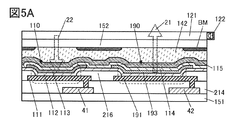
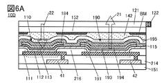
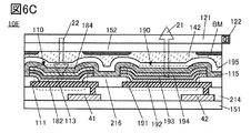
[表示装置の構成例1]
図1Aに、表示装置50の模式図を示す。表示装置50は、基板51、基板52、導光板59、受光素子53、発光素子54、発光素子57R、発光素子57G、発光素子57B、機能層55等を有する。 [Configuration Example 1 of Display Device]
FIG. 1A shows a schematic diagram of thedisplay device 50. The display device 50 includes a substrate 51, a substrate 52, a light guide plate 59, a light receiving element 53, a light emitting element 54, a light emitting element 57R, a light emitting element 57G, a light emitting element 57B, a functional layer 55, and the like.
図1Aに、表示装置50の模式図を示す。表示装置50は、基板51、基板52、導光板59、受光素子53、発光素子54、発光素子57R、発光素子57G、発光素子57B、機能層55等を有する。 [Configuration Example 1 of Display Device]
FIG. 1A shows a schematic diagram of the
発光素子57R、発光素子57G、発光素子57B、及び受光素子53は、基板51と基板52の間に設けられている。
The light emitting element 57R, the light emitting element 57G, the light emitting element 57B, and the light receiving element 53 are provided between the substrate 51 and the substrate 52.
発光素子57R、発光素子57G、発光素子57Bは、それぞれ赤色(R)、緑色(G)、または青色(B)の光を発する。
The light emitting element 57R, the light emitting element 57G, and the light emitting element 57B emit red (R), green (G), or blue (B) light, respectively.
表示装置50は、マトリクス状に配置された複数の画素を有する。1つの画素は、1つ以上の副画素を有する。1つの副画素は、1つの発光素子を有する。例えば、画素には、副画素を3つ有する構成(R、G、Bの3色、または、黄色(Y)、シアン(C)、及びマゼンタ(M)の3色など)、または、副画素を4つ有する構成(R、G、B、白色(W)の4色、または、R、G、B、Yの4色など)を適用できる。さらに、画素は、受光素子53を有する。受光素子53は、全ての画素に設けられていてもよく、一部の画素に設けられていてもよい。また、1つの画素が複数の受光素子53を有していてもよい。
The display device 50 has a plurality of pixels arranged in a matrix. One pixel has one or more sub-pixels. One subpixel has one light emitting element. For example, a pixel has three subpixels (three colors of R, G, and B, or three colors of yellow (Y), cyan (C), and magenta (M)), or a subpixel A configuration having four (R, G, B, four colors of white (W), or four colors of R, G, B, Y, etc.) can be applied. Further, the pixel has a light receiving element 53. The light receiving element 53 may be provided in all the pixels, or may be provided in a part of the pixels. Further, one pixel may have a plurality of light receiving elements 53.
導光板59は、基板52上に設けられている。導光板59としては、可視光及び赤外光に対して高い透光性を有する材料を用いることが好ましい。例えば波長600nmの光、及び波長800nmの光に対する透過率が、共に80%以上、好ましくは85%以上、より好ましくは90%以上、さらに好ましくは95%以上であって、100%以下である材料を用いることができる。
The light guide plate 59 is provided on the substrate 52. As the light guide plate 59, it is preferable to use a material having a high translucency to visible light and infrared light. For example, a material having a transmittance of light having a wavelength of 600 nm and light having a wavelength of 800 nm of 80% or more, preferably 85% or more, more preferably 90% or more, still more preferably 95% or more and 100% or less. Can be used.
また、導光板59は、発光素子54が発する光に対して屈折率の高い材料を用いることが好ましい。例えば、波長800nmの光に対する屈折率が、1.2以上2.5以下、好ましくは1.3以上2.0以下、より好ましくは、1.4以上1.8以下の材料を用いることができる。
Further, the light guide plate 59 is preferably made of a material having a high refractive index with respect to the light emitted from the light emitting element 54. For example, a material having a refractive index of 1.2 or more and 2.5 or less, preferably 1.3 or more and 2.0 or less, and more preferably 1.4 or more and 1.8 or less with respect to light having a wavelength of 800 nm can be used. ..
また、導光板59と基板52とが接して設けられる、またはこれらが樹脂層等で接着されることが好ましい。このとき、導光板59と接する基板52または樹脂層は、少なくとも導光板59に接する部分が、導光板59よりも800nm乃至1000nmの波長範囲の光に対する屈折率が低いことが好ましい。
Further, it is preferable that the light guide plate 59 and the substrate 52 are provided in contact with each other, or these are adhered by a resin layer or the like. At this time, in the substrate 52 or the resin layer in contact with the light guide plate 59, it is preferable that at least a portion in contact with the light guide plate 59 has a lower refractive index for light in the wavelength range of 800 nm to 1000 nm than the light guide plate 59.
発光素子54は、導光板59の側面近傍に設けられる。発光素子54は、導光板59の側面に赤外光IRを発することができる。発光素子54としては、上述した波長の光を含む赤外光を発することのできる発光素子を用いることができる。発光素子54としては、OLED、QLEDなどのEL素子、またはLEDを用いることができる。発光素子54は、導光板59の側面に沿って複数設けられていてもよい。
The light emitting element 54 is provided near the side surface of the light guide plate 59. The light emitting element 54 can emit infrared light IR to the side surface of the light guide plate 59. As the light emitting element 54, a light emitting element capable of emitting infrared light including the above-mentioned wavelength light can be used. As the light emitting element 54, an EL element such as OLED or QLED, or an LED can be used. A plurality of light emitting elements 54 may be provided along the side surface of the light guide plate 59.
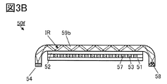
図1Aには、導光板59の表面に指60が触れる様子を示している。導光板59の内部を拡散する赤外光IRの一部は、導光板59と指60との接触部で反射または散乱される。そして、赤外光IRの散乱光IR(r)の一部が、受光素子53に入射されることにより、指60が導光板59に接触したことを検出することができる。すなわち、表示装置50はタッチパネルとして機能することができる。
FIG. 1A shows how the finger 60 touches the surface of the light guide plate 59. A part of the infrared light IR that diffuses inside the light guide plate 59 is reflected or scattered at the contact portion between the light guide plate 59 and the finger 60. Then, when a part of the scattered light IR(r) of the infrared light IR is incident on the light receiving element 53, it is possible to detect that the finger 60 is in contact with the light guide plate 59. That is, the display device 50 can function as a touch panel.
機能層55は、発光素子57R、発光素子57G、発光素子57Bを駆動する回路、及び、受光素子53を駆動する回路を有する。機能層55には、スイッチ、トランジスタ、容量、配線などが設けられる。なお、発光素子57R、発光素子57G、発光素子57B、及び受光素子53をパッシブマトリクス方式で駆動させる場合には、スイッチやトランジスタを設けない構成としてもよい。
The functional layer 55 has a circuit that drives the light emitting element 57R, the light emitting element 57G, and the light emitting element 57B, and a circuit that drives the light receiving element 53. The functional layer 55 is provided with switches, transistors, capacitors, wirings, and the like. Note that when the light-emitting element 57R, the light-emitting element 57G, the light-emitting element 57B, and the light-receiving element 53 are driven by a passive matrix method, a switch or a transistor may not be provided.
表示装置50は、指60の指紋を検出する機能を有していてもよい。図1Bには、導光板59に指60が触れている状態における接触部の拡大図を模式的に示している。また、図1Bには、交互に配列した発光素子57と受光素子53を示している。
The display device 50 may have a function of detecting the fingerprint of the finger 60. FIG. 1B schematically shows an enlarged view of the contact portion when the finger 60 is in contact with the light guide plate 59. Further, FIG. 1B shows the light emitting elements 57 and the light receiving elements 53 arranged alternately.
指60は凹部及び凸部により指紋が形成されている。そのため、図1Bに示すように指紋の凸部が、導光板59に触れ、これらの接触面において、散乱光IR(r)が生じる。
The finger 60 has a fingerprint formed by the concave portion and the convex portion. Therefore, as shown in FIG. 1B, the convex portion of the fingerprint touches the light guide plate 59, and scattered light IR(r) is generated at these contact surfaces.
図1Bに示すように、指60と導光板59の接触面で散乱される散乱光IR(r)は、接触面から等方的に散乱されうる。散乱光IR(r)の強度分布は、概ね接触面に垂直な向きの強度が最も高く、これよりも斜め方向に角度が大きくなるほど低い強度分布となる。したがって、接触面の直下に位置する(接触面と重なる)受光素子53が受光する光の強度が最も高くなる。また、散乱光IR(r)のうち、散乱角が所定の角度以上の光は、図1Bに示すように、導光板59の他方の面(接触面とは反対側の面)で全反射し、受光素子53側には透過しなくなる。
As shown in FIG. 1B, the scattered light IR(r) scattered on the contact surface between the finger 60 and the light guide plate 59 can be isotropically scattered from the contact surface. The intensity distribution of the scattered light IR(r) has the highest intensity in the direction substantially perpendicular to the contact surface, and the intensity distribution becomes lower as the angle in the oblique direction becomes larger than this. Therefore, the intensity of the light received by the light receiving element 53 located immediately below the contact surface (overlapping the contact surface) is the highest. Further, of the scattered light IR(r), light having a scattering angle equal to or larger than a predetermined angle is totally reflected by the other surface (the surface opposite to the contact surface) of the light guide plate 59, as shown in FIG. 1B. The light is not transmitted to the light receiving element 53 side.
受光素子53の配列間隔は、指紋の2つの凸部間の距離、好ましくは隣接する凹部と凸部間の距離よりも小さい間隔とすることで、鮮明な指紋の画像を取得することができる。人の指紋の凹部と凸部の間隔は概ね200μmであることから、例えば受光素子53の配列間隔は、400μm以下、好ましくは200μm以下、より好ましくは150μm以下、さらに好ましくは100μm以下、さらに好ましくは50μm以下であって、1μm以上、好ましくは10μm以上、より好ましくは20μm以上とする。
A clear fingerprint image can be obtained by setting the light-receiving element 53 arrangement interval to be smaller than the distance between two convex portions of the fingerprint, preferably the distance between adjacent concave portions and convex portions. Since the distance between the concave portion and the convex portion of a human fingerprint is approximately 200 μm, for example, the arrangement distance of the light receiving elements 53 is 400 μm or less, preferably 200 μm or less, more preferably 150 μm or less, further preferably 100 μm or less, and further preferably It is 50 μm or less, and 1 μm or more, preferably 10 μm or more, more preferably 20 μm or more.
なお、指60と導光板59との接触面では、赤外光IRの散乱だけでなく反射も生じる場合がある。反射光の反射角は、赤外光IRの入射角によって変化するため、散乱光IR(r)とは強度分布が異なる場合がある。しかしながら、接触面と受光素子53との距離が、受光素子53の配列間隔に対して十分に小さい場合には、散乱光IR(r)と反射光の強度分布の違いは無視できる程度に小さいため、撮像する画像の鮮明さにはほとんど影響しないといえる。
Incidentally, at the contact surface between the finger 60 and the light guide plate 59, not only scattering of the infrared light IR but also reflection may occur. Since the reflection angle of the reflected light changes depending on the incident angle of the infrared light IR, the intensity distribution may be different from that of the scattered light IR(r). However, when the distance between the contact surface and the light receiving element 53 is sufficiently small with respect to the arrangement interval of the light receiving elements 53, the difference between the intensity distributions of the scattered light IR(r) and the reflected light is negligibly small. It can be said that there is almost no effect on the sharpness of the captured image.
表示装置50で撮像した指紋の画像の例を図1Cに示す。図1Cには、撮像範囲63内に、指60の輪郭を破線で、接触部61の輪郭を一点鎖線で示している。接触部61内において、受光素子53に入射する光量の違いによって、コントラストの高い指紋62を撮像することができる。
FIG. 1C shows an example of a fingerprint image taken by the display device 50. In FIG. 1C, the outline of the finger 60 is shown by a broken line, and the outline of the contact portion 61 is shown by a dashed-dotted line in the imaging range 63. In the contact portion 61, the fingerprint 62 having high contrast can be captured due to the difference in the amount of light incident on the light receiving element 53.
表示装置50は、タッチパネルや、ペンタブレットとしても機能させることができる。図1Dには、スタイラス65の先端を導光板59に接触させた状態で、破線矢印の方向に滑らせている様子を示している。
The display device 50 can also function as a touch panel or a pen tablet. FIG. 1D shows a state in which the tip of the stylus 65 is in contact with the light guide plate 59 and is slid in the direction of the broken line arrow.
図1Dに示すように、スタイラス65の先端と、導光板59の接触面で散乱される散乱光IR(r)が、当該散乱面と重なる部分に位置する受光素子53に入射することで、スタイラス65の先端の位置を高精度に検出することができる。
As shown in FIG. 1D, the scattered light IR(r) scattered by the tip of the stylus 65 and the contact surface of the light guide plate 59 is incident on the light receiving element 53 located in a portion overlapping the scattering surface, whereby the stylus is formed. The position of the tip of 65 can be detected with high accuracy.
図1Eには、表示装置50で検出したスタイラス65の軌跡66の例を示している。表示装置50は、高い位置精度でスタイラス65等の被検出体の位置検出が可能であるため、描画アプリケーション等において、高精細な描画を行うことも可能である。
FIG. 1E shows an example of the locus 66 of the stylus 65 detected by the display device 50. Since the display device 50 can detect the position of the detection target such as the stylus 65 with high position accuracy, it is also possible to perform high-definition drawing in a drawing application or the like.
ここで、図1F乃至図1Hに、表示装置50に適用可能な画素30の一例を示す。
Here, FIGS. 1F to 1H show an example of the pixel 30 applicable to the display device 50.
図1F及び図1Gに示す画素30は、それぞれ表示のための副画素として機能する、赤色(R)の画素31R、緑色(G)の画素31G、青色(B)の画素31Bと、受光画素として機能する画素32を有する。画素31R、画素31G、画素31Bは、それぞれ発光素子57R、発光素子57G、または発光素子57Bを一以上有する。画素32は、受光素子53を一以上有する。
A pixel 30 shown in FIGS. 1F and 1G functions as a sub-pixel for display, and serves as a red (R) pixel 31R, a green (G) pixel 31G, a blue (B) pixel 31B, and a light receiving pixel. It has a functional pixel 32. The pixel 31R, the pixel 31G, and the pixel 31B each include one or more light emitting elements 57R, 57G, or 57B. The pixel 32 has one or more light receiving elements 53.
図1Fは、2×2のマトリクス状に、3つの副画素と画素32が配置されている例である。図1Gは、横一列に、3つの副画素と画素32が配置されている例である。
FIG. 1F is an example in which three subpixels and pixels 32 are arranged in a 2×2 matrix. FIG. 1G is an example in which three sub-pixels and pixels 32 are arranged in a horizontal row.
図1Hに示す画素30は、白色(W)の画素31Wを有する例である。画素31Wは、白色の発光素子を一以上有する。ここでは、4つの副画素が横一列に配置され、その下側に画素32が配置されている。
The pixel 30 shown in FIG. 1H is an example having a white (W) pixel 31W. The pixel 31W has one or more white light emitting elements. Here, four sub-pixels are arranged in a horizontal row, and the pixel 32 is arranged below the sub-pixels.
なお、画素の構成は上記に限られず、様々な配置方法を採用することができる。
Note that the pixel configuration is not limited to the above, and various arrangement methods can be adopted.
[表示装置の構成例2]
以下では、上記とは一部の構成が異なる表示装置の構成例について説明する。 [Configuration Example 2 of Display Device]
In the following, a configuration example of a display device that is partially different from the above configuration will be described.
以下では、上記とは一部の構成が異なる表示装置の構成例について説明する。 [Configuration Example 2 of Display Device]
In the following, a configuration example of a display device that is partially different from the above configuration will be described.
〔構成例2−1〕
図2Aに示す表示装置50aは、上記表示装置50と比較して、基板52に換えて樹脂層71を有する点で、主に相違している。 [Configuration example 2-1]
The display device 50a shown in FIG. 2A mainly differs from thedisplay device 50 described above in that a resin layer 71 is provided instead of the substrate 52.
図2Aに示す表示装置50aは、上記表示装置50と比較して、基板52に換えて樹脂層71を有する点で、主に相違している。 [Configuration example 2-1]
The display device 50a shown in FIG. 2A mainly differs from the
樹脂層71は、可視光に対して透光性を有する材料を用いることができる。また、樹脂層71は、基板51と導光板59とを接着する機能を有していてもよい。
The resin layer 71 may be made of a material that transmits visible light. Further, the resin layer 71 may have a function of bonding the substrate 51 and the light guide plate 59.
樹脂層71は、導光板59と接して設けられる。ここで、樹脂層71は、少なくとも導光板59と接する部分において、導光板59よりも800nm乃至1000nmの波長範囲の光に対する屈折率が低いことが好ましい。これにより、図2Aに示すように、導光板59と樹脂層71との界面で赤外光IRを全反射させることができる。
The resin layer 71 is provided in contact with the light guide plate 59. Here, it is preferable that the resin layer 71 has a lower refractive index for light in the wavelength range of 800 nm to 1000 nm than the light guide plate 59, at least in the portion in contact with the light guide plate 59. Thereby, as shown in FIG. 2A, the infrared light IR can be totally reflected at the interface between the light guide plate 59 and the resin layer 71.
〔構成例2−2〕
図2Bに示す表示装置50bは、導電層72を有する点で、上記表示装置50aと主に相違している。 [Structure example 2-2]
Thedisplay device 50b shown in FIG. 2B mainly differs from the display device 50a in that it has a conductive layer 72.
図2Bに示す表示装置50bは、導電層72を有する点で、上記表示装置50aと主に相違している。 [Structure example 2-2]
The
導電層72は、導光板59に接して設けられている。ここでは、導電層72が導光板59と樹脂層71との間に位置する例を示している。
The conductive layer 72 is provided in contact with the light guide plate 59. Here, an example is shown in which the conductive layer 72 is located between the light guide plate 59 and the resin layer 71.
導電層72に、所定の電位を与えることで、静電遮蔽膜として機能させることができる。導電層72により、外部から導光板59を介して入力される電気的なノイズが、表示装置50bが有する回路などに到達することを好適に防ぐことができる。
By applying a predetermined potential to the conductive layer 72, it can function as an electrostatic shield film. The conductive layer 72 can preferably prevent electrical noise input from the outside through the light guide plate 59 from reaching a circuit or the like included in the display device 50b.
また、導電層72は、タッチセンサなどのセンサ素子の電極として機能させることもできる。特に、静電容量方式のタッチセンサの電極として用いることが好ましい。
The conductive layer 72 can also function as an electrode of a sensor element such as a touch sensor. In particular, it is preferably used as an electrode of a capacitance type touch sensor.
導電層72は、可視光を透過する導電性材料を用いることができる。また、導電層72に、発光素子54が発する赤外光IRを透過する導電性材料を好適に用いることができる。
The conductive layer 72 can be made of a conductive material that transmits visible light. Further, for the conductive layer 72, a conductive material that transmits the infrared light IR emitted by the light emitting element 54 can be preferably used.
導電層72は、少なくとも導光板59と接する部分において、導光板59よりも800nm乃至1000nmの波長範囲の光に対する屈折率が高い導電性材料を用いることが好ましい。これにより、図2Bに示すように、赤外光IRは導光板59だけでなく導電層72の内部も拡散する構成とすることができる。また、導電層72は樹脂層71よりも上述の波長範囲の光に対する屈折率が高いため、赤外光IRを、導電層72と樹脂層71との界面で全反射させることができる。
The conductive layer 72 is preferably made of a conductive material having a higher refractive index for light in the wavelength range of 800 nm to 1000 nm than that of the light guide plate 59, at least in a portion in contact with the light guide plate 59. As a result, as shown in FIG. 2B, the infrared light IR can be diffused not only in the light guide plate 59 but also inside the conductive layer 72. Further, since the conductive layer 72 has a higher refractive index than the resin layer 71 with respect to light in the above wavelength range, the infrared light IR can be totally reflected at the interface between the conductive layer 72 and the resin layer 71.
なお、ここでは樹脂層71を有する例を示したが、基板52を有する構成としてもよい。
Although an example having the resin layer 71 is shown here, a configuration having the substrate 52 may be used.
〔構成例2−3〕
図2Cに示す表示装置50cは、発光素子57R等と、受光素子53とが、異なる面上に設けられている例を示している。表示装置50cは、基板51a、基板51b、機能層55a、機能層55b等を有する。 [Structure example 2-3]
Thedisplay device 50c shown in FIG. 2C shows an example in which the light emitting element 57R and the like and the light receiving element 53 are provided on different surfaces. The display device 50c includes a substrate 51a, a substrate 51b, a functional layer 55a, a functional layer 55b, and the like.
図2Cに示す表示装置50cは、発光素子57R等と、受光素子53とが、異なる面上に設けられている例を示している。表示装置50cは、基板51a、基板51b、機能層55a、機能層55b等を有する。 [Structure example 2-3]
The
機能層55aは、発光素子57R等を駆動する回路を有する層であり、基板51aに設けられている。また、機能層55bは、受光素子53を駆動する回路を有する層であり、基板51b上に設けられている。基板51aと基板51bとは、図示しない接着層等で固定されていることが好ましい。
The functional layer 55a is a layer having a circuit for driving the light emitting element 57R and the like, and is provided on the substrate 51a. The functional layer 55b is a layer having a circuit for driving the light receiving element 53, and is provided on the substrate 51b. The substrate 51a and the substrate 51b are preferably fixed by an adhesive layer or the like (not shown).
このとき、受光素子53が有する活性層には、シリコンなどの無機半導体材料を用いることができる。このとき、活性層には、赤外光IRの波長に応じて、単結晶シリコン、多結晶シリコン、またはアモルファスシリコンなどを選択して用いることができる。なお、ここでは、機能層55b及び受光素子53を、基板51b上に積層する例を示しているが、基板51bに半導体基板を用いた場合には、基板51bが機能層55b及び受光素子53の一部を成していてもよい。
At this time, an inorganic semiconductor material such as silicon can be used for the active layer of the light receiving element 53. At this time, single crystal silicon, polycrystalline silicon, amorphous silicon, or the like can be selected and used for the active layer depending on the wavelength of the infrared light IR. Here, an example in which the functional layer 55b and the light receiving element 53 are stacked on the substrate 51b is shown, but when a semiconductor substrate is used as the substrate 51b, the substrate 51b includes the functional layer 55b and the light receiving element 53. It may form a part.
〔構成例2−4〕
図2Dに示す表示装置50dは、発光素子57R等と受光素子53とが、機能層55を挟んで設けられている点で、表示装置50cと主に相違している。 [Structure example 2-4]
Thedisplay device 50d illustrated in FIG. 2D mainly differs from the display device 50c in that the light emitting element 57R and the light receiving element 53 are provided with the functional layer 55 interposed therebetween.
図2Dに示す表示装置50dは、発光素子57R等と受光素子53とが、機能層55を挟んで設けられている点で、表示装置50cと主に相違している。 [Structure example 2-4]
The
受光素子53が有する活性層には、上述したシリコンなどの無機半導体材料を用いることができる。また、基板51として半導体基板を用いた場合には、基板51が受光素子53の活性層などの一部を成していてもよい。
The above-described inorganic semiconductor material such as silicon can be used for the active layer of the light receiving element 53. When a semiconductor substrate is used as the substrate 51, the substrate 51 may form part of the active layer of the light receiving element 53 or the like.
なお、表示装置50c及び表示装置50dにおいて、基板52に換えて樹脂層71を設ける構成としてもよいし、導電層72を有する構成としてもよい。
In the display device 50c and the display device 50d, the resin layer 71 may be provided instead of the substrate 52, or the conductive layer 72 may be provided.
[導光板の構成例]
本発明の一態様の表示装置に適用可能な導光板は、例えば電子機器の表示部に設けられ、表示面やタッチ面として機能する筐体の一部を兼ねることもできる。このとき、導光板は、発光素子や受光素子、機能層などを保護する保護部材としても機能する。例えば強化ガラスや、可撓性を有するフィルムなどを、導光板として用いることができる。 [Example of light guide plate configuration]
The light guide plate applicable to the display device of one embodiment of the present invention can be provided in, for example, a display portion of an electronic device and can also serve as part of a housing functioning as a display surface or a touch surface. At this time, the light guide plate also functions as a protective member that protects the light emitting element, the light receiving element, the functional layer, and the like. For example, tempered glass, a flexible film, or the like can be used as the light guide plate.
図3Aに、表示装置50eの構成例を示す。表示装置50eは、基板52上に導光板59aが設けられた構成を有する。図3Aは、平板状の導光板59aを有する例である。
FIG. 3A shows a configuration example of the display device 50e. The display device 50e has a configuration in which a light guide plate 59a is provided on the substrate 52. FIG. 3A is an example having a flat light guide plate 59a.
導光板59aは、一方の端部に沿って、赤外光IRを発する発光素子54が配置されている。また、導光板59aの発光素子54が設けられる側とは反対側には、反射層58が設けられている。反射層58は、赤外光IRを反射する機能を有する。反射層58を設けることにより、導光板59a内を拡散する赤外光IRの強度分布を均一化させることができる。
The light guide plate 59a has a light emitting element 54 that emits infrared light IR arranged along one end. Further, a reflective layer 58 is provided on the side of the light guide plate 59a opposite to the side on which the light emitting element 54 is provided. The reflective layer 58 has a function of reflecting the infrared light IR. By providing the reflection layer 58, the intensity distribution of the infrared light IR diffused in the light guide plate 59a can be made uniform.
図3Bには、両端が湾曲した導光板59bを有する表示装置50fの構成例を示している。
FIG. 3B shows a configuration example of a display device 50f having a light guide plate 59b whose both ends are curved.
導光板59bは、導光板59aと同様に、一方の端部に沿って発光素子54が設けられ、他方の端部に沿って反射層58が設けられている。導光板59bの内部には赤外光IRが拡散している。
Like the light guide plate 59a, the light guide plate 59b is provided with the light emitting element 54 along one end and the reflection layer 58 along the other end. Infrared light IR is diffused inside the light guide plate 59b.
導光板59bの両端を湾曲させ、その端部に沿って発光素子54や反射層58を設ける構成とすることで、表示装置50fを適用した電子機器における表示部を囲う非表示領域(額縁ともいう)の面積を小さくできるため好ましい。
A non-display area (also referred to as a frame) that surrounds the display unit in the electronic device to which the display device 50f is applied is configured by bending both ends of the light guide plate 59b and providing the light emitting element 54 and the reflective layer 58 along the ends. It is preferable because the area of 1) can be reduced.
ここで、導光板59bの湾曲部では、赤外光IRの一部が全反射せずに外部に射出されてしまい、導光板59b内に拡散する赤外光IRの強度が低下してしまう場合がある。しかしながら、導光板59bを十分に薄くすること等により、赤外光IRの全反射が生じる割合を高めることができる。例えば導光板59bの厚さを、2mm以下、好ましくは1mm以下、より好ましくは0.8mm以下、さらに好ましくは0.7mm以下であって、10μm以上、好ましくは30μm以上、より好ましくは50μm以上とすることで、導光板59b内の赤外光IRの強度の低下を抑制することができる。
Here, in the curved portion of the light guide plate 59b, a part of the infrared light IR is emitted to the outside without being totally reflected, and the intensity of the infrared light IR diffused in the light guide plate 59b is reduced. There is. However, by making the light guide plate 59b sufficiently thin or the like, it is possible to increase the proportion of total reflection of the infrared light IR. For example, the thickness of the light guide plate 59b is 2 mm or less, preferably 1 mm or less, more preferably 0.8 mm or less, still more preferably 0.7 mm or less, and 10 μm or more, preferably 30 μm or more, more preferably 50 μm or more. By doing so, it is possible to suppress a decrease in the intensity of the infrared light IR in the light guide plate 59b.
図3Cには、一部が湾曲した導光板59cに沿って、基板51等が湾曲して設けられる、表示装置50gの構成例を示している。
FIG. 3C shows a configuration example of a display device 50g in which the substrate 51 and the like are provided in a curved manner along a partially curved light guide plate 59c.
基板51は、可撓性を有する材料を用いることができる。導光板59cの湾曲部の曲率半径が十分に大きい場合には、基板51にガラス基板などの無機絶縁基板を用いることができる。また、基板51として、有機樹脂などを含む材料を用いることが好ましい。
The substrate 51 can be made of a flexible material. When the radius of curvature of the curved portion of the light guide plate 59c is sufficiently large, an inorganic insulating substrate such as a glass substrate can be used as the substrate 51. Further, it is preferable to use a material containing an organic resin or the like for the substrate 51.
また、図3Cでは、基板51と導光板59cとを、樹脂層71で接着している例を示している。このように、導光板59cの湾曲面に沿って基板51を配置する場合には、基板52を設けずに樹脂層71で接着する構成とすると、基板51と導光板59cとの貼り合せを容易にできるため好ましい。またこれだけでなく、受光素子53と導光板59cとの距離を近づけることができるため、位置検出の精度が高まることや、鮮明な撮像が行える、といった相乗的な効果を奏する。
Further, FIG. 3C shows an example in which the substrate 51 and the light guide plate 59c are bonded by the resin layer 71. In this way, when the substrate 51 is arranged along the curved surface of the light guide plate 59c, if the resin layer 71 is adhered without providing the substrate 52, the substrate 51 and the light guide plate 59c can be easily attached. It is preferable because it can be In addition to this, since the distance between the light receiving element 53 and the light guide plate 59c can be reduced, the position detection accuracy can be increased and a clear image can be obtained.
なお、図3Cでは、導光板59cが、湾曲した部分と、平坦な部分とを有する例を示したが、平坦な部分を有さずに、全体が湾曲した形状であってもよい。
Although FIG. 3C shows an example in which the light guide plate 59c has a curved portion and a flat portion, it may have a curved shape without the flat portion.
以上が、導光板の構成例についての説明である。
The above is a description of a configuration example of the light guide plate.
[表示装置の構成例3]
以下では、本発明の一態様の表示装置のより具体的な例について説明する。 [Configuration Example 3 of Display Device]
Hereinafter, more specific examples of the display device of one embodiment of the present invention will be described.
以下では、本発明の一態様の表示装置のより具体的な例について説明する。 [Configuration Example 3 of Display Device]
Hereinafter, more specific examples of the display device of one embodiment of the present invention will be described.
〔構成例3−1〕
図4Aに、表示装置10Aの断面概略図を示す。 [Configuration example 3-1]
FIG. 4A shows a schematic sectional view of thedisplay device 10A.
図4Aに、表示装置10Aの断面概略図を示す。 [Configuration example 3-1]
FIG. 4A shows a schematic sectional view of the
表示装置10Aは、受光素子110及び発光素子190を有する。受光素子110は、画素電極111、共通層112、活性層113、共通層114、及び共通電極115を有する。発光素子190は、画素電極191、共通層112、発光層193、共通層114、及び共通電極115を有する。
The display device 10A has a light receiving element 110 and a light emitting element 190. The light receiving element 110 has a pixel electrode 111, a common layer 112, an active layer 113, a common layer 114, and a common electrode 115. The light emitting element 190 has a pixel electrode 191, a common layer 112, a light emitting layer 193, a common layer 114, and a common electrode 115.
画素電極111、画素電極191、共通層112、活性層113、発光層193、共通層114、及び共通電極115は、それぞれ、単層構造であってもよく、積層構造であってもよい。
Each of the pixel electrode 111, the pixel electrode 191, the common layer 112, the active layer 113, the light emitting layer 193, the common layer 114, and the common electrode 115 may have a single-layer structure or a laminated structure.
画素電極111及び画素電極191は、絶縁層214上に位置する。画素電極111と画素電極191は、同一の材料及び同一の工程で形成することができる。
The pixel electrode 111 and the pixel electrode 191 are located on the insulating layer 214. The pixel electrode 111 and the pixel electrode 191 can be formed using the same material and the same process.
共通層112は、画素電極111上及び画素電極191上に位置する。共通層112は、受光素子110と発光素子190に共通で用いられる層である。
The common layer 112 is located on the pixel electrode 111 and the pixel electrode 191. The common layer 112 is a layer commonly used by the light receiving element 110 and the light emitting element 190.
活性層113は、共通層112を介して、画素電極111と重なる。発光層193は、共通層112を介して、画素電極191と重なる。活性層113は、第1の有機化合物を有し、発光層193は、第1の有機化合物とは異なる第2の有機化合物を有する。
The active layer 113 overlaps the pixel electrode 111 via the common layer 112. The light emitting layer 193 overlaps with the pixel electrode 191 via the common layer 112. The active layer 113 has a first organic compound, and the light emitting layer 193 has a second organic compound different from the first organic compound.
共通層114は、共通層112上、活性層113上、及び発光層193上に位置する。共通層114は、受光素子110と発光素子190に共通で用いられる層である。
The common layer 114 is located on the common layer 112, the active layer 113, and the light emitting layer 193. The common layer 114 is a layer commonly used by the light receiving element 110 and the light emitting element 190.
共通電極115は、共通層112、活性層113、及び共通層114を介して、画素電極111と重なる部分を有する。また、共通電極115は、共通層112、発光層193、及び共通層114を介して、画素電極191と重なる部分を有する。共通電極115は、受光素子110と発光素子190に共通で用いられる層である。
The common electrode 115 has a portion which overlaps with the pixel electrode 111 with the common layer 112, the active layer 113, and the common layer 114 interposed therebetween. Further, the common electrode 115 has a portion overlapping with the pixel electrode 191 with the common layer 112, the light emitting layer 193, and the common layer 114 interposed therebetween. The common electrode 115 is a layer commonly used by the light receiving element 110 and the light emitting element 190.
本実施の形態の表示装置では、受光素子110の活性層113に有機化合物を用いる。受光素子110は、活性層113以外の層を、発光素子190(EL素子)と共通の構成にすることができる。そのため、発光素子190の作製工程に、活性層113を成膜する工程を追加するのみで、発光素子190の形成と並行して受光素子110を形成することができる。また、発光素子190と受光素子110とを同一基板上に形成することができる。したがって、作製工程を大幅に増やすことなく、表示装置に受光素子110を内蔵することができる。
In the display device of this embodiment, an organic compound is used for the active layer 113 of the light receiving element 110. In the light receiving element 110, layers other than the active layer 113 can have the same configuration as the light emitting element 190 (EL element). Therefore, the light receiving element 110 can be formed in parallel with the formation of the light emitting element 190 only by adding the step of forming the active layer 113 to the manufacturing step of the light emitting element 190. Further, the light emitting element 190 and the light receiving element 110 can be formed on the same substrate. Therefore, the light receiving element 110 can be incorporated in the display device without significantly increasing the number of manufacturing steps.
表示装置10Aでは、受光素子110の活性層113と、発光素子190の発光層193と、を作り分ける以外は、受光素子110と発光素子190が共通の構成である例を示す。ただし、受光素子110と発光素子190の構成はこれに限定されない。受光素子110と発光素子190は、活性層113と発光層193のほかにも、互いに作り分ける層を有していてもよい(後述の表示装置10D、10E、10F参照)。受光素子110と発光素子190は、共通で用いられる層(共通層)を1層以上有することが好ましい。これにより、作製工程を大幅に増やすことなく、表示装置に受光素子110を内蔵することができる。
In the display device 10A, an example is shown in which the light receiving element 110 and the light emitting element 190 have a common configuration except that the active layer 113 of the light receiving element 110 and the light emitting layer 193 of the light emitting element 190 are formed separately. However, the configurations of the light receiving element 110 and the light emitting element 190 are not limited to this. The light-receiving element 110 and the light-emitting element 190 may have layers separately formed in addition to the active layer 113 and the light-emitting layer 193 (see display devices 10D, 10E, and 10F described later). It is preferable that the light receiving element 110 and the light emitting element 190 have one or more layers that are used in common (common layer). Accordingly, the light receiving element 110 can be incorporated in the display device without significantly increasing the number of manufacturing steps.
表示装置10Aは、一対の基板(基板151及び基板152)間に、受光素子110、発光素子190、トランジスタ41、及びトランジスタ42等を有する。
The display device 10A includes a light receiving element 110, a light emitting element 190, a transistor 41, a transistor 42, and the like between a pair of substrates (the substrate 151 and the substrate 152).
また、表示装置10Aは、基板152よりも外側に、導光板121を有する。導光板121の端部には、赤外光を発する発光素子122が配置されている。
Further, the display device 10A has a light guide plate 121 outside the substrate 152. A light emitting element 122 that emits infrared light is arranged at an end of the light guide plate 121.
受光素子110において、それぞれ画素電極111及び共通電極115の間に位置する共通層112、活性層113、及び共通層114は、有機層(有機化合物を含む層)ということもできる。画素電極111は可視光及び赤外光を反射する機能を有することが好ましい。画素電極111の端部は隔壁216によって覆われている。共通電極115は可視光及び赤外光を透過する機能を有する。
In the light receiving element 110, the common layer 112, the active layer 113, and the common layer 114, which are located between the pixel electrode 111 and the common electrode 115, respectively, can be referred to as organic layers (layers containing an organic compound). The pixel electrode 111 preferably has a function of reflecting visible light and infrared light. An end portion of the pixel electrode 111 is covered with a partition wall 216. The common electrode 115 has a function of transmitting visible light and infrared light.
受光素子110は、光を検出する機能を有する。具体的には、受光素子110は、導光板121から入射される光22を受光し、電気信号に変換する、光電変換素子である。
The light receiving element 110 has a function of detecting light. Specifically, the light receiving element 110 is a photoelectric conversion element that receives the light 22 incident from the light guide plate 121 and converts the light 22 into an electric signal.
基板152の基板151側の面には、遮光層BMが設けられている。遮光層BMは、受光素子110と重なる位置及び発光素子190と重なる位置に開口を有する。遮光層BMを設けることで、受光素子110が光を検出する範囲を制御することができる。
A light shielding layer BM is provided on the surface of the substrate 152 on the substrate 151 side. The light-blocking layer BM has openings at positions where it overlaps with the light receiving element 110 and at positions where it overlaps with the light emitting element 190. By providing the light shielding layer BM, the range in which the light receiving element 110 detects light can be controlled.
遮光層BMとしては、発光素子からの発光を遮る材料を用いることができる。遮光層BMは、可視光を吸収することが好ましい。遮光層BMとして、例えば、金属材料、又は、顔料(カーボンブラックなど)もしくは染料を含む樹脂材料等を用いてブラックマトリクスを形成することができる。遮光層BMは、赤色のカラーフィルタ、緑色のカラーフィルタ、及び青色のカラーフィルタの積層構造であってもよい。
A material that blocks light emitted from the light emitting element can be used for the light shielding layer BM. The light shielding layer BM preferably absorbs visible light. As the light-shielding layer BM, for example, a black matrix can be formed using a metal material, a resin material containing a pigment (such as carbon black) or a dye, or the like. The light blocking layer BM may have a laminated structure of a red color filter, a green color filter, and a blue color filter.
ここで、受光素子110は、導光板121の表面で散乱された光を検出する。しかし、発光素子190の発光が、表示装置10A内で反射され、導光板121等を介さずに、受光素子110に入射されてしまう場合がある。遮光層BMは、このような迷光の影響を抑制することができる。例えば、遮光層BMが設けられていない場合、発光素子190が発した光23aは、基板152で反射され、反射光23bが受光素子110に入射することがある。遮光層BMを設けることで、反射光23bが受光素子110に入射することを抑制できる。これにより、ノイズを低減し、受光素子110を用いたセンサの感度を高めることができる。
Here, the light receiving element 110 detects the light scattered on the surface of the light guide plate 121. However, the light emitted from the light emitting element 190 may be reflected in the display device 10A and enter the light receiving element 110 without passing through the light guide plate 121 and the like. The light shielding layer BM can suppress such an influence of stray light. For example, when the light shielding layer BM is not provided, the light 23a emitted by the light emitting element 190 may be reflected by the substrate 152 and the reflected light 23b may enter the light receiving element 110. By providing the light shielding layer BM, it is possible to suppress the reflected light 23b from entering the light receiving element 110. Thereby, noise can be reduced and the sensitivity of the sensor using the light receiving element 110 can be increased.
発光素子190において、それぞれ画素電極191及び共通電極115の間に位置する共通層112、発光層193、及び共通層114は、EL層ということもできる。画素電極191は可視光及び赤外光を反射する機能を有することが好ましい。画素電極191の端部は隔壁216によって覆われている。画素電極111と画素電極191とは隔壁216によって互いに電気的に絶縁されている。共通電極115は可視光及び赤外光を透過する機能を有する。
In the light emitting element 190, the common layer 112, the light emitting layer 193, and the common layer 114, which are located between the pixel electrode 191 and the common electrode 115, respectively, can also be referred to as EL layers. The pixel electrode 191 preferably has a function of reflecting visible light and infrared light. An end portion of the pixel electrode 191 is covered with a partition wall 216. The pixel electrode 111 and the pixel electrode 191 are electrically insulated from each other by the partition wall 216. The common electrode 115 has a function of transmitting visible light and infrared light.
発光素子190は、可視光を発する機能を有する。具体的には、発光素子190は、画素電極191と共通電極115との間に電圧を印加することで、基板152側に光21を射出する電界発光素子である。
The light emitting element 190 has a function of emitting visible light. Specifically, the light emitting element 190 is an electroluminescent element that emits the light 21 to the substrate 152 side by applying a voltage between the pixel electrode 191 and the common electrode 115.
発光層193は、受光素子110の受光領域と重ならないように形成されることが好ましい。これにより、発光層193が光22を吸収することを抑制でき、受光素子110に照射される光量を多くすることができる。
The light emitting layer 193 is preferably formed so as not to overlap the light receiving region of the light receiving element 110. Thereby, the light emitting layer 193 can be suppressed from absorbing the light 22, and the amount of light with which the light receiving element 110 is irradiated can be increased.
画素電極111は、絶縁層214に設けられた開口を介して、トランジスタ41が有するソースまたはドレインと電気的に接続される。画素電極111の端部は、隔壁216によって覆われている。
The pixel electrode 111 is electrically connected to the source or the drain of the transistor 41 through the opening provided in the insulating layer 214. The end of the pixel electrode 111 is covered with a partition 216.
画素電極191は、絶縁層214に設けられた開口を介して、トランジスタ42が有するソースまたはドレインと電気的に接続される。画素電極191の端部は、隔壁216によって覆われている。トランジスタ42は、発光素子190の駆動を制御する機能を有する。
The pixel electrode 191 is electrically connected to the source or the drain of the transistor 42 through the opening provided in the insulating layer 214. The end portion of the pixel electrode 191 is covered with a partition wall 216. The transistor 42 has a function of controlling driving of the light emitting element 190.
トランジスタ41とトランジスタ42とは、同一の層(図4Aでは基板151)上に接している。
The transistor 41 and the transistor 42 are in contact with each other on the same layer (the substrate 151 in FIG. 4A).
受光素子110と電気的に接続される回路の少なくとも一部は、発光素子190と電気的に接続される回路と同一の材料及び同一の工程で形成されることが好ましい。これにより、2つの回路を別々に形成する場合に比べて、表示装置の厚さを薄くすることができ、また、作製工程を簡略化できる。
At least a part of the circuit electrically connected to the light receiving element 110 is preferably formed of the same material and the same process as the circuit electrically connected to the light emitting element 190. Accordingly, the thickness of the display device can be reduced and the manufacturing process can be simplified as compared with the case where two circuits are formed separately.
受光素子110及び発光素子190は、それぞれ、保護層195に覆われていることが好ましい。図4Aでは、保護層195が、共通電極115上に接して設けられている。保護層195を設けることで、受光素子110及び発光素子190に水などの不純物が入り込むことを抑制し、受光素子110及び発光素子190の信頼性を高めることができる。また、接着層142によって、保護層195と基板152とが貼り合わされている。
Each of the light receiving element 110 and the light emitting element 190 is preferably covered with a protective layer 195. In FIG. 4A, the protective layer 195 is provided on and in contact with the common electrode 115. By providing the protective layer 195, impurities such as water can be prevented from entering the light receiving element 110 and the light emitting element 190, and the reliability of the light receiving element 110 and the light emitting element 190 can be improved. Further, the protective layer 195 and the substrate 152 are attached to each other by the adhesive layer 142.
なお、図5Aに示すように、受光素子110上及び発光素子190上に保護層を有していなくてもよい。図5Aでは、接着層142によって、共通電極115と基板152とが貼り合わされている。
Note that, as shown in FIG. 5A, the light receiving element 110 and the light emitting element 190 may not have a protective layer. In FIG. 5A, the common electrode 115 and the substrate 152 are attached to each other by the adhesive layer 142.
また、図5Bに示すように、遮光層BMを有さない構成としてもよい。これにより、受光素子110の受光面積を大きくできるため、よりセンサの感度を高めることができる。
Further, as shown in FIG. 5B, a configuration without the light shielding layer BM may be adopted. As a result, the light receiving area of the light receiving element 110 can be increased, and the sensitivity of the sensor can be further increased.
〔構成例3−2〕
図4Bに表示装置10Bの断面図を示す。なお、以降の表示装置の説明において、先に説明した表示装置と同様の構成については、説明を省略することがある。 [Structure example 3-2]
FIG. 4B shows a sectional view of thedisplay device 10B. Note that in the following description of the display device, description of the same configuration as the display device described above may be omitted.
図4Bに表示装置10Bの断面図を示す。なお、以降の表示装置の説明において、先に説明した表示装置と同様の構成については、説明を省略することがある。 [Structure example 3-2]
FIG. 4B shows a sectional view of the
図4Bに示す表示装置10Bは、表示装置10Aの構成に加え、レンズ149を有する。
The display device 10B shown in FIG. 4B has a lens 149 in addition to the configuration of the display device 10A.
レンズ149は、受光素子110と重なる位置に設けられている。表示装置10Bでは、レンズ149が基板152に接して設けられている。表示装置10Bが有するレンズ149は、基板151側に凸面を有する凸レンズである。なお、基板152側に凸面を有する凸レンズを、受光素子110と重なる領域に配置してもよい。
The lens 149 is provided at a position overlapping the light receiving element 110. In the display device 10B, the lens 149 is provided in contact with the substrate 152. The lens 149 included in the display device 10B is a convex lens having a convex surface on the substrate 151 side. A convex lens having a convex surface on the substrate 152 side may be arranged in a region overlapping with the light receiving element 110.
基板152の同一面上に遮光層BMとレンズ149との双方を形成する場合、形成順は問わない。図4Bでは、レンズ149を先に形成する例を示すが、遮光層BMを先に形成してもよい。図4Bでは、レンズ149の端部が遮光層BMによって覆われている。
When both the light shielding layer BM and the lens 149 are formed on the same surface of the substrate 152, the formation order does not matter. Although FIG. 4B shows an example in which the lens 149 is formed first, the light shielding layer BM may be formed first. In FIG. 4B, the end portion of the lens 149 is covered with the light shielding layer BM.
表示装置10Bは、光22がレンズ149を介して受光素子110に入射する構成である。レンズ149を有すると、レンズ149を有さない場合に比べて、受光素子110の撮像範囲を狭くすることができ、隣接する受光素子110と撮像範囲が重なることを抑制できる。これにより、ぼやけの少ない、鮮明な画像を撮像できる。また、受光素子110の撮像範囲が同じ場合、レンズ149を有すると、レンズ149を有さない場合に比べて、ピンホールの大きさ(図4Bでは受光素子110と重なるBMの開口の大きさに相当する)を大きくすることができる。したがって、レンズ149を有することで、受光素子110に入射する光量を増やすことができる。
The display device 10B is configured such that the light 22 is incident on the light receiving element 110 via the lens 149. With the lens 149, it is possible to narrow the image pickup range of the light receiving element 110 as compared with the case where the lens 149 is not provided, and it is possible to suppress overlapping of the image pickup range with the adjacent light receiving element 110. This makes it possible to capture a clear image with little blur. Further, when the image pickup range of the light receiving element 110 is the same, when the lens 149 is provided, the size of the pinhole is larger than that in the case where the lens 149 is not provided (in FIG. Equivalent) can be increased. Therefore, by including the lens 149, the amount of light incident on the light receiving element 110 can be increased.
本実施の形態の表示装置に用いるレンズの形成方法としては、基板上または受光素子上にマイクロレンズなどのレンズを直接形成してもよいし、別途作製されたマイクロレンズアレイなどのレンズアレイを基板に貼り合わせてもよい。
As a method for forming a lens used in the display device of this embodiment mode, a lens such as a microlens may be directly formed over a substrate or a light-receiving element, or a lens array such as a separately manufactured microlens array may be formed on the substrate. It may be attached to.
〔構成例3−3〕
図4Cに、表示装置10Cの断面概略図を示す。表示装置10Cは、基板151、基板152、及び隔壁216を有さず、基板153、基板154、接着層155、絶縁層212、及び隔壁217を有する点で、表示装置10Aと異なる。 [Structure example 3-3]
FIG. 4C shows a schematic cross-sectional view of the display device 10C. The display device 10C is different from thedisplay device 10A in that the display device 10C does not have the substrate 151, the substrate 152, and the partition wall 216, but has the substrate 153, the substrate 154, the adhesive layer 155, the insulating layer 212, and the partition wall 217.
図4Cに、表示装置10Cの断面概略図を示す。表示装置10Cは、基板151、基板152、及び隔壁216を有さず、基板153、基板154、接着層155、絶縁層212、及び隔壁217を有する点で、表示装置10Aと異なる。 [Structure example 3-3]
FIG. 4C shows a schematic cross-sectional view of the display device 10C. The display device 10C is different from the
基板153と絶縁層212とは接着層155によって貼り合わされている。基板154と保護層195とは接着層142によって貼り合わされている。
The substrate 153 and the insulating layer 212 are attached by the adhesive layer 155. The substrate 154 and the protective layer 195 are attached to each other with the adhesive layer 142.
表示装置10Cは、作製基板上に形成された絶縁層212、トランジスタ41、トランジスタ42、受光素子110、及び発光素子190等を、基板153上に転置することで作製される構成である。基板153及び基板154は、それぞれ、可撓性を有することが好ましい。これにより、表示装置10Cの可撓性を高めることができる。例えば、基板153及び基板154には、それぞれ、樹脂を用いることが好ましい。
The display device 10C has a structure manufactured by transferring the insulating layer 212, the transistor 41, the transistor 42, the light receiving element 110, the light emitting element 190, and the like formed over the manufacturing substrate onto the substrate 153. It is preferable that each of the substrate 153 and the substrate 154 have flexibility. Thereby, the flexibility of the display device 10C can be enhanced. For example, resin is preferably used for each of the substrate 153 and the substrate 154.
基板153及び基板154としては、それぞれ、ポリエチレンテレフタレート(PET)、ポリエチレンナフタレート(PEN)等のポリエステル樹脂、ポリアクリロニトリル樹脂、アクリル樹脂、ポリイミド樹脂、ポリメチルメタクリレート樹脂、ポリカーボネート(PC)樹脂、ポリエーテルスルホン(PES)樹脂、ポリアミド樹脂(ナイロン、アラミド等)、ポリシロキサン樹脂、シクロオレフィン樹脂、ポリスチレン樹脂、ポリアミドイミド樹脂、ポリウレタン樹脂、ポリ塩化ビニル樹脂、ポリ塩化ビニリデン樹脂、ポリプロピレン樹脂、ポリテトラフルオロエチレン(PTFE)樹脂、ABS樹脂、セルロースナノファイバー等を用いることができる。基板153及び基板154の一方または双方に、可撓性を有する程度の厚さのガラスを用いてもよい。
As the substrate 153 and the substrate 154, polyester resin such as polyethylene terephthalate (PET) and polyethylene naphthalate (PEN), polyacrylonitrile resin, acrylic resin, polyimide resin, polymethylmethacrylate resin, polycarbonate (PC) resin, polyether are used. Sulfone (PES) resin, polyamide resin (nylon, aramid, etc.), polysiloxane resin, cycloolefin resin, polystyrene resin, polyamideimide resin, polyurethane resin, polyvinyl chloride resin, polyvinylidene chloride resin, polypropylene resin, polytetrafluoroethylene (PTFE) resin, ABS resin, cellulose nanofiber, etc. can be used. One or both of the substrate 153 and the substrate 154 may be formed of glass having a thickness such that the glass has flexibility.
本実施の形態の表示装置が有する基板には、光学等方性が高いフィルムを用いてもよい。光学等方性が高いフィルムとしては、トリアセチルセルロース(TAC、セルローストリアセテートともいう)フィルム、シクロオレフィンポリマー(COP)フィルム、シクロオレフィンコポリマー(COC)フィルム、及びアクリルフィルム等が挙げられる。
A film having high optical isotropy may be used for the substrate included in the display device of this embodiment. Examples of the film having high optical isotropy include a triacetyl cellulose (TAC, also called cellulose triacetate) film, a cycloolefin polymer (COP) film, a cycloolefin copolymer (COC) film, and an acrylic film.
隔壁217は、発光素子が発した光を吸収することが好ましい。隔壁217として、例えば、顔料もしくは染料を含む樹脂材料等を用いてブラックマトリクスを形成することができる。また、茶色レジスト材料を用いることで、着色された絶縁層で隔壁217を構成することができる。
The partition wall 217 preferably absorbs the light emitted by the light emitting element. As the partition wall 217, for example, a black matrix can be formed using a resin material containing a pigment or a dye. Further, by using a brown resist material, the partition wall 217 can be formed using a colored insulating layer.
発光素子190が発した光23cは、基板152及び隔壁217で反射され、反射光23dが受光素子110に入射することがある。また、光23cが隔壁217を透過し、トランジスタまたは配線等で反射されることで、反射光が受光素子110に入射することがある。隔壁217によって光23cが吸収されることで、反射光23dが受光素子110に入射することを抑制できる。これにより、ノイズを低減し、受光素子110を用いたセンサの感度を高めることができる。
The light 23c emitted from the light emitting element 190 may be reflected by the substrate 152 and the partition wall 217, and the reflected light 23d may enter the light receiving element 110. Further, the light 23c may pass through the partition wall 217 and be reflected by the transistor, the wiring, or the like, so that the reflected light may enter the light receiving element 110. Since the light 23c is absorbed by the partition wall 217, the reflected light 23d can be suppressed from entering the light receiving element 110. Thereby, noise can be reduced and the sensitivity of the sensor using the light receiving element 110 can be increased.
隔壁217は、少なくとも、受光素子110が検出する光の波長を吸収することが好ましい。例えば、発光素子190が発する赤色の光を受光素子110が検出する場合、隔壁217は、少なくとも赤色の光を吸収することが好ましい。例えば、隔壁217が、青色のカラーフィルタを有すると、赤色の光23cを吸収することができ、反射光23dが受光素子110に入射することを抑制できる。
The partition wall 217 preferably absorbs at least the wavelength of light detected by the light receiving element 110. For example, when the light receiving element 110 detects red light emitted from the light emitting element 190, the partition wall 217 preferably absorbs at least red light. For example, when the partition wall 217 has a blue color filter, the red light 23c can be absorbed, and the reflected light 23d can be suppressed from entering the light receiving element 110.
〔構成例3−4〕
上記では、発光素子と受光素子が、2つの共通層を有する例を示したが、これに限られない。以下では、共通層の構成が異なる例について説明する。 [Structure example 3-4]
In the above, the example in which the light emitting element and the light receiving element have two common layers is shown, but the invention is not limited to this. Hereinafter, an example in which the configuration of the common layer is different will be described.
図6Aに、表示装置10Dの断面概略図を示す。表示装置10Dは、共通層114を有さず、バッファ層184及びバッファ層194を有する点で、表示装置10Aと異なる。バッファ層184及びバッファ層194は、それぞれ、単層構造であってもよく、積層構造であってもよい。
FIG. 6A shows a schematic sectional view of the display device 10D. The display device 10D is different from the display device 10A in that it does not have the common layer 114 but has the buffer layer 184 and the buffer layer 194. The buffer layer 184 and the buffer layer 194 may each have a single layer structure or a stacked structure.
表示装置10Dにおいて、受光素子110は、画素電極111、共通層112、活性層113、バッファ層184、及び共通電極115を有する。また、表示装置10Dにおいて、発光素子190は、画素電極191、共通層112、発光層193、バッファ層194、及び共通電極115を有する。
In the display device 10D, the light receiving element 110 has a pixel electrode 111, a common layer 112, an active layer 113, a buffer layer 184, and a common electrode 115. Further, in the display device 10D, the light emitting element 190 includes the pixel electrode 191, the common layer 112, the light emitting layer 193, the buffer layer 194, and the common electrode 115.
表示装置10Dでは、共通電極115と活性層113との間のバッファ層184と、共通電極115と発光層193との間のバッファ層194とを作り分ける例を示す。バッファ層184及びバッファ層194としては、例えば、電子注入層及び電子輸送層の一方または双方を形成することができる。
In the display device 10D, an example in which a buffer layer 184 between the common electrode 115 and the active layer 113 and a buffer layer 194 between the common electrode 115 and the light emitting layer 193 are separately formed are shown. As the buffer layer 184 and the buffer layer 194, for example, one or both of an electron injection layer and an electron transport layer can be formed.
図6Bに、表示装置10Eの断面概略図を示す。表示装置10Eは、共通層112を有さず、バッファ層182及びバッファ層192を有する点で、表示装置10Aと異なる。バッファ層182及びバッファ層192は、それぞれ、単層構造であってもよく、積層構造であってもよい。
FIG. 6B shows a schematic sectional view of the display device 10E. The display device 10E is different from the display device 10A in that the display device 10E does not have the common layer 112 but has the buffer layer 182 and the buffer layer 192. The buffer layer 182 and the buffer layer 192 may each have a single-layer structure or a stacked structure.
表示装置10Eにおいて、受光素子110は、画素電極111、バッファ層182、活性層113、共通層114、及び共通電極115を有する。また、表示装置10Eにおいて、発光素子190は、画素電極191、バッファ層192、発光層193、共通層114、及び共通電極115を有する。
In the display device 10E, the light receiving element 110 has a pixel electrode 111, a buffer layer 182, an active layer 113, a common layer 114, and a common electrode 115. In addition, in the display device 10E, the light emitting element 190 includes the pixel electrode 191, the buffer layer 192, the light emitting layer 193, the common layer 114, and the common electrode 115.
表示装置10Eでは、画素電極111と活性層113との間のバッファ層182と、画素電極191と発光層193との間のバッファ層192とを作り分ける例を示す。バッファ層182及びバッファ層192としては、例えば、正孔注入層及び正孔輸送層の一方または双方を形成することができる。
In the display device 10E, an example is shown in which a buffer layer 182 between the pixel electrode 111 and the active layer 113 and a buffer layer 192 between the pixel electrode 191 and the light emitting layer 193 are formed separately. As the buffer layer 182 and the buffer layer 192, for example, one or both of a hole injection layer and a hole transport layer can be formed.
図6Cに、表示装置10Fの断面概略図を示す。表示装置10Fは、共通層112及び共通層114を有さず、バッファ層182、バッファ層184、バッファ層192、及びバッファ層194を有する点で、表示装置10Aと異なる。
FIG. 6C shows a schematic sectional view of the display device 10F. The display device 10F is different from the display device 10A in that the display device 10F does not have the common layer 112 and the common layer 114 but has the buffer layer 182, the buffer layer 184, the buffer layer 192, and the buffer layer 194.
表示装置10Fにおいて、受光素子110は、画素電極111、バッファ層182、活性層113、バッファ層184、及び共通電極115を有する。また、表示装置10Fにおいて、発光素子190は、画素電極191、バッファ層192、発光層193、バッファ層194、及び共通電極115を有する。
In the display device 10F, the light receiving element 110 has a pixel electrode 111, a buffer layer 182, an active layer 113, a buffer layer 184, and a common electrode 115. Further, in the display device 10F, the light emitting element 190 includes the pixel electrode 191, the buffer layer 192, the light emitting layer 193, the buffer layer 194, and the common electrode 115.
受光素子110と発光素子190の作製において、活性層113と発光層193を作り分けるだけでなく、他の層も作り分けることができる。
In manufacturing the light receiving element 110 and the light emitting element 190, not only the active layer 113 and the light emitting layer 193 can be formed separately, but also other layers can be formed separately.
表示装置10Fでは、受光素子110と発光素子190とで、一対の電極(画素電極111または画素電極191と共通電極115)間に、共通の層を有さない例を示す。表示装置10Fが有する受光素子110及び発光素子190は、絶縁層214上に画素電極111と画素電極191とを同一の材料及び同一の工程で形成し、画素電極111上にバッファ層182、活性層113、及びバッファ層184を、画素電極191上にバッファ層192、発光層193、及びバッファ層194を、それぞれ形成した後に、バッファ層184及びバッファ層194等を覆うように共通電極115を形成することで作製できる。
The display device 10F shows an example in which the light receiving element 110 and the light emitting element 190 do not have a common layer between a pair of electrodes (the pixel electrode 111 or the pixel electrode 191 and the common electrode 115). In the light receiving element 110 and the light emitting element 190 included in the display device 10F, the pixel electrode 111 and the pixel electrode 191 are formed on the insulating layer 214 by the same material and in the same process, and the buffer layer 182 and the active layer are formed on the pixel electrode 111. 113, the buffer layer 184, the buffer layer 192, the light emitting layer 193, and the buffer layer 194 are formed over the pixel electrode 191, respectively, and then the common electrode 115 is formed so as to cover the buffer layer 184, the buffer layer 194, and the like. It can be made by
なお、バッファ層182、活性層113、及びバッファ層184の積層構造と、バッファ層192、発光層193、及びバッファ層194の積層構造の作製順は特に限定されない。例えば、バッファ層182、活性層113、及びバッファ層184を成膜した後に、バッファ層192、発光層193、及びバッファ層194を作製してもよい。逆に、バッファ層182、活性層113、及びバッファ層184を成膜する前に、バッファ層192、発光層193、及びバッファ層194を作製してもよい。また、バッファ層182、バッファ層192、活性層113、発光層193、などの順に交互に成膜してもよい。
Note that the stacking structure of the buffer layer 182, the active layer 113, and the buffer layer 184 and the stacking structure of the buffer layer 192, the light emitting layer 193, and the buffer layer 194 are not particularly limited. For example, after forming the buffer layer 182, the active layer 113, and the buffer layer 184, the buffer layer 192, the light emitting layer 193, and the buffer layer 194 may be formed. On the contrary, the buffer layer 192, the light emitting layer 193, and the buffer layer 194 may be formed before forming the buffer layer 182, the active layer 113, and the buffer layer 184. Alternatively, the buffer layer 182, the buffer layer 192, the active layer 113, the light emitting layer 193, and the like may be alternately formed in this order.
[表示装置の構成例4]
以下では、本発明の一態様の表示装置のより具体的な構成例について説明する。 [Configuration Example 4 of Display Device]
Hereinafter, a more specific structural example of the display device of one embodiment of the present invention will be described.
以下では、本発明の一態様の表示装置のより具体的な構成例について説明する。 [Configuration Example 4 of Display Device]
Hereinafter, a more specific structural example of the display device of one embodiment of the present invention will be described.
〔構成例4−1〕
図7に、表示装置100Aの斜視図を示す。 [Configuration Example 4-1]
FIG. 7 shows a perspective view of thedisplay device 100A.
図7に、表示装置100Aの斜視図を示す。 [Configuration Example 4-1]
FIG. 7 shows a perspective view of the
表示装置100Aは、基板151と基板152とが貼り合された構成を有する。また、基板152上に導光板121が設けられている。図7では、基板152と導光板121を破線で示している。
The display device 100A has a configuration in which a substrate 151 and a substrate 152 are attached to each other. Further, the light guide plate 121 is provided on the substrate 152. In FIG. 7, the substrate 152 and the light guide plate 121 are indicated by broken lines.
表示装置100Aは、表示部162、回路164、配線165等を有する。図7では、表示装置100AにIC(集積回路)173及びFPC172が実装されている例を示している。そのため、図7に示す構成は、表示装置100A、IC、及びFPCを有する表示モジュールということもできる。
The display device 100A includes a display portion 162, a circuit 164, a wiring 165, and the like. FIG. 7 shows an example in which an IC (integrated circuit) 173 and an FPC 172 are mounted on the display device 100A. Therefore, the configuration illustrated in FIG. 7 can be referred to as a display module including the display device 100A, an IC, and an FPC.
回路164としては、走査線駆動回路を用いることができる。
A scan line driver circuit can be used as the circuit 164.
配線165は、表示部162及び回路164に信号及び電力を供給する機能を有する。当該信号及び電力は、FPC172を介して外部から入力されるか、またはIC173から配線165に入力される。
The wiring 165 has a function of supplying a signal and power to the display portion 162 and the circuit 164. The signal and power are externally input via the FPC 172 or input from the IC 173 to the wiring 165.
図7では、COG(Chip On Glass)方式またはCOF(Chip On Film)方式などにより、基板151にIC173が設けられている例を示す。IC173は、例えば走査線駆動回路及び信号線駆動回路等を有するICを適用できる。なお、表示装置100A及び表示モジュールは、ICを設けない構成としてもよい。また、ICを、COF方式等により、FPCに実装してもよい。
FIG. 7 shows an example in which the IC 173 is provided on the substrate 151 by the COG (Chip On Glass) method or the COF (Chip On Film) method. As the IC 173, for example, an IC including a scan line driver circuit, a signal line driver circuit, and the like can be applied. Note that the display device 100A and the display module may not have an IC. Further, the IC may be mounted on the FPC by the COF method or the like.
図8に、図7で示した表示装置100Aの、FPC172を含む領域の一部、回路164を含む領域の一部、表示部162を含む領域の一部、及び、端部を含む領域の一部をそれぞれ切断したときの断面の一例を示す。
FIG. 8 illustrates a part of a region including the FPC 172, a part of a region including the circuit 164, a part of a region including the display portion 162, and a region including an end portion of the display device 100A illustrated in FIG. An example of the cross section when each part is cut is shown.
図8に示す表示装置100Aは、基板151と基板152の間に、トランジスタ201、トランジスタ205、トランジスタ206、発光素子190、受光素子110等を有する。また基板152上に、導光板121が設けられている。導光板121の端部には、発光素子122が設けられている。
The display device 100A shown in FIG. 8 includes a transistor 201, a transistor 205, a transistor 206, a light emitting element 190, a light receiving element 110, and the like between a substrate 151 and a substrate 152. Further, the light guide plate 121 is provided on the substrate 152. A light emitting element 122 is provided at an end of the light guide plate 121.
基板152と絶縁層214は接着層142を介して接着されている。発光素子190及び受光素子110の封止には、固体封止構造または中空封止構造などが適用できる。図8では、基板152、接着層142、及び絶縁層214に囲まれた空間143が、不活性ガス(窒素やアルゴンなど)で充填されており、中空封止構造が適用されている。接着層142は、発光素子190と重ねて設けられていてもよい。また、基板152、接着層142、及び絶縁層214に囲まれた空間143を、接着層142とは異なる樹脂で充填してもよい。
The substrate 152 and the insulating layer 214 are adhered via the adhesive layer 142. For sealing the light emitting element 190 and the light receiving element 110, a solid sealing structure, a hollow sealing structure, or the like can be applied. In FIG. 8, the space 143 surrounded by the substrate 152, the adhesive layer 142, and the insulating layer 214 is filled with an inert gas (nitrogen, argon, or the like), and a hollow sealing structure is applied. The adhesive layer 142 may be provided so as to overlap with the light emitting element 190. Further, the space 143 surrounded by the substrate 152, the adhesive layer 142, and the insulating layer 214 may be filled with a resin different from that of the adhesive layer 142.
発光素子190は、絶縁層214側から画素電極191、共通層112、発光層193、共通層114、及び共通電極115の順に積層された積層構造を有する。画素電極191は、絶縁層214に設けられた開口を介して、トランジスタ206が有する導電層222bと接続されている。トランジスタ206は、発光素子190の駆動を制御する機能を有する。画素電極191の端部は、隔壁216によって覆われている。画素電極191は可視光及び赤外光を反射する材料を含み、共通電極115は可視光及び赤外光を透過する材料を含む。
The light emitting element 190 has a laminated structure in which the pixel electrode 191, the common layer 112, the light emitting layer 193, the common layer 114, and the common electrode 115 are laminated in this order from the insulating layer 214 side. The pixel electrode 191 is connected to the conductive layer 222b included in the transistor 206 through an opening provided in the insulating layer 214. The transistor 206 has a function of controlling driving of the light emitting element 190. The end portion of the pixel electrode 191 is covered with a partition wall 216. The pixel electrode 191 includes a material that reflects visible light and infrared light, and the common electrode 115 includes a material that transmits visible light and infrared light.
受光素子110は、絶縁層214側から画素電極111、共通層112、活性層113、共通層114、及び共通電極115の順に積層された積層構造を有する。画素電極111は、絶縁層214に設けられた開口を介して、トランジスタ205が有する導電層222bと電気的に接続されている。画素電極111の端部は、隔壁216によって覆われている。画素電極111は可視光及び赤外光を反射する材料を含み、共通電極115は可視光及び赤外光を透過する材料を含む。
The light receiving element 110 has a laminated structure in which the pixel electrode 111, the common layer 112, the active layer 113, the common layer 114, and the common electrode 115 are laminated in this order from the insulating layer 214 side. The pixel electrode 111 is electrically connected to the conductive layer 222b included in the transistor 205 through an opening provided in the insulating layer 214. The end of the pixel electrode 111 is covered with a partition 216. The pixel electrode 111 includes a material that reflects visible light and infrared light, and the common electrode 115 includes a material that transmits visible light and infrared light.
発光素子190が発する光は、基板152側に射出される。また、受光素子110には、基板152及び空間143を介して、光が入射する。基板152には、可視光及び赤外光に対する透過性が高い材料を用いることが好ましい。
The light emitted from the light emitting element 190 is emitted to the substrate 152 side. Further, light enters the light receiving element 110 via the substrate 152 and the space 143. For the substrate 152, it is preferable to use a material having high transparency to visible light and infrared light.
画素電極111及び画素電極191は同一の材料及び同一の工程で作製することができる。共通層112、共通層114、及び共通電極115は、受光素子110と発光素子190との双方に用いられる。受光素子110と発光素子190とは、活性層113と発光層193の構成が異なる以外は全て共通の構成とすることができる。これにより、作製工程を大幅に増やすことなく、表示装置100Aに受光素子110を内蔵することができる。
The pixel electrode 111 and the pixel electrode 191 can be manufactured using the same material and the same process. The common layer 112, the common layer 114, and the common electrode 115 are used for both the light receiving element 110 and the light emitting element 190. The light receiving element 110 and the light emitting element 190 may have a common configuration except that the configurations of the active layer 113 and the light emitting layer 193 are different. Accordingly, the light receiving element 110 can be incorporated in the display device 100A without significantly increasing the number of manufacturing steps.
基板152の基板151側の面には、遮光層BMが設けられている。遮光層BMは、受光素子110と重なる位置及び発光素子190と重なる位置に開口を有する。遮光層BMを設けることで、受光素子110が光を検出する範囲を制御することができる。また、遮光層BMを有することで、発光素子190から受光素子110に光が直接入射することを抑制できる。したがって、ノイズが少なく感度の高いセンサを実現できる。
A light shielding layer BM is provided on the surface of the substrate 152 on the substrate 151 side. The light-blocking layer BM has openings at positions where it overlaps with the light receiving element 110 and at positions where it overlaps with the light emitting element 190. By providing the light shielding layer BM, the range in which the light receiving element 110 detects light can be controlled. In addition, since the light shielding layer BM is provided, it is possible to prevent light from directly entering the light receiving element 110 from the light emitting element 190. Therefore, a sensor with less noise and high sensitivity can be realized.
トランジスタ201、トランジスタ205、及びトランジスタ206は、いずれも基板151上に形成されている。これらのトランジスタは、同一の材料及び同一の工程により作製することができる。
The transistors 201, 205, and 206 are all formed on the substrate 151. These transistors can be manufactured using the same material and the same process.
基板151上には、絶縁層211、絶縁層213、絶縁層215、及び絶縁層214がこの順で設けられている。絶縁層211は、その一部が各トランジスタのゲート絶縁層として機能する。絶縁層213は、その一部が各トランジスタのゲート絶縁層として機能する。絶縁層215は、トランジスタを覆って設けられる。絶縁層214は、トランジスタを覆って設けられ、平坦化層としての機能を有する。なお、ゲート絶縁層の数及びトランジスタを覆う絶縁層の数は限定されず、それぞれ単層であっても2層以上であってもよい。
The insulating layer 211, the insulating layer 213, the insulating layer 215, and the insulating layer 214 are provided in this order on the substrate 151. A part of the insulating layer 211 functions as a gate insulating layer of each transistor. Part of the insulating layer 213 functions as a gate insulating layer of each transistor. The insulating layer 215 is provided so as to cover the transistor. The insulating layer 214 is provided so as to cover the transistor and has a function as a planarization layer. Note that the number of gate insulating layers and the number of insulating layers covering the transistor are not limited, and each may be a single layer or two or more layers.
トランジスタを覆う絶縁層の少なくとも一層に、水や水素などの不純物が拡散しにくい材料を用いることが好ましい。これにより、絶縁層をバリア層として機能させることができる。このような構成とすることで、トランジスタに外部から不純物が拡散することを効果的に抑制でき、表示装置の信頼性を高めることができる。
It is preferable to use a material in which impurities such as water and hydrogen do not easily diffuse for at least one of the insulating layers covering the transistor. This allows the insulating layer to function as a barrier layer. With such a structure, diffusion of impurities into the transistor from the outside can be effectively suppressed, and reliability of the display device can be improved.
絶縁層211、絶縁層213、及び絶縁層215としては、それぞれ、無機絶縁膜を用いることが好ましい。無機絶縁膜としては、例えば、窒化シリコン膜、酸化窒化シリコン膜、酸化シリコン膜、窒化酸化シリコン膜、酸化アルミニウム膜、窒化アルミニウム膜などの無機絶縁膜を用いることができる。また、酸化ハフニウム膜、酸化イットリウム膜、酸化ジルコニウム膜、酸化ガリウム膜、酸化タンタル膜、酸化マグネシウム膜、酸化ランタン膜、酸化セリウム膜、及び酸化ネオジム膜等を用いてもよい。また、上述の絶縁膜を2以上積層して用いてもよい。
It is preferable to use an inorganic insulating film as each of the insulating layer 211, the insulating layer 213, and the insulating layer 215. As the inorganic insulating film, for example, an inorganic insulating film such as a silicon nitride film, a silicon oxynitride film, a silicon oxide film, a silicon nitride oxide film, an aluminum oxide film, or an aluminum nitride film can be used. Alternatively, a hafnium oxide film, a yttrium oxide film, a zirconium oxide film, a gallium oxide film, a tantalum oxide film, a magnesium oxide film, a lanthanum oxide film, a cerium oxide film, a neodymium oxide film, or the like may be used. Further, two or more of the above-mentioned insulating films may be laminated and used.
ここで、有機絶縁膜は、無機絶縁膜に比べてバリア性が低いことが多い。そのため、有機絶縁膜は、表示装置100Aの端部近傍に開口を有することが好ましい。これにより、表示装置100Aの端部から有機絶縁膜を介して不純物が拡散することを抑制することができる。または、有機絶縁膜の端部が表示装置100Aの端部よりも内側に位置するように有機絶縁膜を形成し、表示装置100Aの端部に有機絶縁膜が露出しないようにしてもよい。
Here, the organic insulating film often has a lower barrier property than the inorganic insulating film. Therefore, the organic insulating film preferably has an opening near the end of the display device 100A. This can prevent impurities from diffusing from the end portion of the display device 100A through the organic insulating film. Alternatively, the organic insulating film may be formed so that the end portion of the organic insulating film is located inside the end portion of the display device 100A so that the organic insulating film is not exposed at the end portion of the display device 100A.
平坦化層として機能する絶縁層214には、有機絶縁膜が好適である。有機絶縁膜に用いることができる材料としては、アクリル樹脂、ポリイミド樹脂、エポキシ樹脂、ポリアミド樹脂、ポリイミドアミド樹脂、シロキサン樹脂、ベンゾシクロブテン系樹脂、フェノール樹脂、及びこれら樹脂の前駆体等が挙げられる。
An organic insulating film is suitable for the insulating layer 214 that functions as a flattening layer. Materials that can be used for the organic insulating film include acrylic resin, polyimide resin, epoxy resin, polyamide resin, polyimide amide resin, siloxane resin, benzocyclobutene resin, phenol resin, and precursors of these resins. ..
図8に示す領域228では、絶縁層214に開口が形成されている。これにより、絶縁層214に有機絶縁膜を用いる場合であっても、絶縁層214を介して外部から表示部162に不純物が拡散することを抑制できる。したがって、表示装置100Aの信頼性を高めることができる。
In the region 228 shown in FIG. 8, an opening is formed in the insulating layer 214. Accordingly, even when an organic insulating film is used for the insulating layer 214, it is possible to prevent impurities from diffusing from the outside to the display portion 162 via the insulating layer 214. Therefore, the reliability of the display device 100A can be improved.
トランジスタ201、トランジスタ205、及びトランジスタ206は、ゲートとして機能する導電層221、ゲート絶縁層として機能する絶縁層211、ソース及びドレインとして機能する導電層222a及び導電層222b、半導体層231、ゲート絶縁層として機能する絶縁層213、並びに、ゲートとして機能する導電層223を有する。ここでは、同一の導電膜を加工して得られる複数の層に、同じハッチングパターンを付している。絶縁層211は、導電層221と半導体層231との間に位置する。絶縁層213は、導電層223と半導体層231との間に位置する。
The transistor 201, the transistor 205, and the transistor 206 include a conductive layer 221 functioning as a gate, an insulating layer 211 functioning as a gate insulating layer, conductive layers 222a and 222b functioning as a source and a drain, a semiconductor layer 231, and a gate insulating layer. The insulating layer 213 that functions as a gate and the conductive layer 223 that functions as a gate are included. Here, the same hatching pattern is given to a plurality of layers obtained by processing the same conductive film. The insulating layer 211 is located between the conductive layer 221 and the semiconductor layer 231. The insulating layer 213 is located between the conductive layer 223 and the semiconductor layer 231.
本実施の形態の表示装置が有するトランジスタの構造は特に限定されない。例えば、プレーナ型のトランジスタ、スタガ型のトランジスタ、逆スタガ型のトランジスタ等を用いることができる。また、トップゲート型またはボトムゲート型のいずれのトランジスタ構造としてもよい。または、チャネルが形成される半導体層の上下にゲートが設けられていてもよい。
The structure of the transistor included in the display device of this embodiment is not particularly limited. For example, a planar transistor, a staggered transistor, an inverted staggered transistor, or the like can be used. Further, either a top-gate or bottom-gate transistor structure may be used. Alternatively, gates may be provided above and below a semiconductor layer in which a channel is formed.
トランジスタ201、トランジスタ205、及びトランジスタ206には、チャネルが形成される半導体層を2つのゲートで挟持する構成が適用されている。2つのゲートを接続し、これらに同一の信号を供給することによりトランジスタを駆動してもよい。または、2つのゲートのうち、一方に閾値電圧を制御するための電位を与え、他方に駆動のための電位を与えることで、トランジスタの閾値電圧を制御してもよい。
A structure in which a semiconductor layer in which a channel is formed is sandwiched between two gates is applied to the transistor 201, the transistor 205, and the transistor 206. The transistor may be driven by connecting two gates and supplying the same signal to them. Alternatively, the threshold voltage of the transistor may be controlled by supplying one of the two gates with a potential for controlling the threshold voltage and the other with a potential for driving.
トランジスタに用いる半導体材料の結晶性についても特に限定されず、非晶質半導体、単結晶半導体、または単結晶以外の結晶性を有する半導体(微結晶半導体、多結晶半導体、または一部に結晶領域を有する半導体)のいずれを用いてもよい。単結晶半導体または結晶性を有する半導体を用いると、トランジスタ特性の劣化を抑制できるため好ましい。
The crystallinity of a semiconductor material used for a transistor is not particularly limited, and an amorphous semiconductor, a single crystal semiconductor, or a semiconductor having crystallinity other than single crystal (a microcrystalline semiconductor, a polycrystalline semiconductor, or a part of which has a crystalline region) is used. Any of the above semiconductors) may be used. It is preferable to use a single crystal semiconductor or a semiconductor having crystallinity because deterioration of transistor characteristics can be suppressed.
トランジスタの半導体層は、金属酸化物(酸化物半導体ともいう)を有することが好ましい。または、トランジスタの半導体層は、シリコンを有していてもよい。シリコンとしては、アモルファスシリコン、結晶性のシリコン(低温ポリシリコン、単結晶シリコンなど)などが挙げられる。
The semiconductor layer of the transistor preferably contains a metal oxide (also referred to as an oxide semiconductor). Alternatively, the semiconductor layer of the transistor may include silicon. Examples of silicon include amorphous silicon and crystalline silicon (low temperature polysilicon, single crystal silicon, etc.).
半導体層は、例えば、インジウムと、M(Mは、ガリウム、アルミニウム、シリコン、ホウ素、イットリウム、スズ、銅、バナジウム、ベリリウム、チタン、鉄、ニッケル、ゲルマニウム、ジルコニウム、モリブデン、ランタン、セリウム、ネオジム、ハフニウム、タンタル、タングステン、及びマグネシウムから選ばれた一種または複数種)と、亜鉛と、を有することが好ましい。特に、Mは、アルミニウム、ガリウム、イットリウム、及びスズから選ばれた一種または複数種であることが好ましい。
The semiconductor layer is, for example, indium and M (M is gallium, aluminum, silicon, boron, yttrium, tin, copper, vanadium, beryllium, titanium, iron, nickel, germanium, zirconium, molybdenum, lanthanum, cerium, neodymium, It is preferable to have zinc and one or more kinds selected from hafnium, tantalum, tungsten, and magnesium). Particularly, M is preferably one or more selected from aluminum, gallium, yttrium, and tin.
特に、半導体層として、インジウム(In)、ガリウム(Ga)、及び亜鉛(Zn)を含む酸化物(IGZOとも記す)を用いることが好ましい。
In particular, it is preferable to use an oxide containing indium (In), gallium (Ga), and zinc (Zn) (also referred to as IGZO) for the semiconductor layer.
半導体層がIn−M−Zn酸化物の場合、In−M−Zn酸化物を成膜するために用いるスパッタリングターゲットは、Mに対するInの原子数比が1以上であることが好ましい。このようなスパッタリングターゲットの金属元素の原子数比として、In:M:Zn=1:1:1、In:M:Zn=1:1:1.2、In:M:Zn=2:1:3、In:M:Zn=3:1:2、In:M:Zn=4:2:3、In:M:Zn=4:2:4.1、In:M:Zn=5:1:6、In:M:Zn=5:1:7、In:M:Zn=5:1:8、In:M:Zn=6:1:6、In:M:Zn=5:2:5等が挙げられる。
When the semiconductor layer is an In-M-Zn oxide, the sputtering target used for forming the In-M-Zn oxide preferably has an atomic ratio of In to M of 1 or more. As the atomic ratio of the metal elements of such a sputtering target, In:M:Zn=1:1:1, In:M:Zn=1:1:1.2, In:M:Zn=2:1:. 3, In:M:Zn=3:1:2, In:M:Zn=4:2:3, In:M:Zn=4:2:4.1, In:M:Zn=5:1: 6, In:M:Zn=5:1:7, In:M:Zn=5:1:8, In:M:Zn=6:1:6, In:M:Zn=5:2:5, etc. Are listed.
スパッタリングターゲットとしては、多結晶の酸化物を含むターゲットを用いると、結晶性を有する半導体層を形成しやすくなるため好ましい。なお、成膜される半導体層の原子数比は、上記のスパッタリングターゲットに含まれる金属元素の原子数比のプラスマイナス40%の変動を含む。例えば、半導体層に用いるスパッタリングターゲットの組成がIn:Ga:Zn=4:2:4.1[原子数比]の場合、成膜される半導体層の組成は、In:Ga:Zn=4:2:3[原子数比]の近傍となる場合がある。
As a sputtering target, it is preferable to use a target containing a polycrystalline oxide because a semiconductor layer having crystallinity can be easily formed. The atomic ratio of the semiconductor layer to be formed includes a fluctuation of ±40% in the atomic ratio of the metal element contained in the sputtering target. For example, when the composition of the sputtering target used for the semiconductor layer is In:Ga:Zn=4:2:4.1 [atomic ratio], the composition of the formed semiconductor layer is In:Ga:Zn=4: It may be in the vicinity of 2:3 [atomic ratio].
なお、原子数比がIn:Ga:Zn=4:2:3またはその近傍と記載する場合、Inの原子数比を4としたとき、Gaの原子数比が1以上3以下であり、Znの原子数比が2以上4以下である場合を含む。また、原子数比がIn:Ga:Zn=5:1:6またはその近傍であると記載する場合、Inの原子数比を5としたときに、Gaの原子数比が0.1より大きく2以下であり、Znの原子数比が5以上7以下である場合を含む。また、原子数比がIn:Ga:Zn=1:1:1またはその近傍であると記載する場合、Inの原子数比を1としたときに、Gaの原子数比が0.1より大きく2以下であり、Znの原子数比が0.1より大きく2以下である場合を含む。
When the atomic ratio is In:Ga:Zn=4:2:3 or in the vicinity thereof, when the atomic ratio of In is 4, the atomic ratio of Ga is 1 or more and 3 or less. The case where the atomic ratio of is 2 or more and 4 or less is included. Further, when describing that the atomic ratio is In:Ga:Zn=5:1:6 or in the vicinity thereof, when the atomic ratio of In is 5, the atomic ratio of Ga is larger than 0.1. It is 2 or less, including the case where the atomic ratio of Zn is 5 or more and 7 or less. Further, when describing that the atomic ratio is In:Ga:Zn=1:1:1 or in the vicinity thereof, when the atomic ratio of In is 1, the atomic ratio of Ga is larger than 0.1. It is 2 or less and includes the case where the atomic ratio of Zn is more than 0.1 and 2 or less.
回路164が有するトランジスタと、表示部162が有するトランジスタは、同じ構造であってもよく、異なる構造であってもよい。回路164が有する複数のトランジスタの構造は、全て同じであってもよく、2種類以上あってもよい。同様に、表示部162が有する複数のトランジスタの構造は、全て同じであってもよく、2種類以上あってもよい。
The transistor included in the circuit 164 and the transistor included in the display portion 162 may have the same structure or different structures. The plurality of transistors included in the circuit 164 may have the same structure or may have two or more types. Similarly, the structures of the plurality of transistors included in the display portion 162 may be all the same or may be two or more.
基板151の、基板152が重ならない領域には、接続部204が設けられている。接続部204では、配線165が導電層166及び接続層242を介してFPC172と電気的に接続されている。接続部204の上面は、画素電極191と同一の導電膜を加工して得られた導電層166が露出している。これにより、接続部204とFPC172とを接続層242を介して電気的に接続することができる。
A connection portion 204 is provided in a region of the substrate 151 where the substrate 152 does not overlap. In the connection portion 204, the wiring 165 is electrically connected to the FPC 172 via the conductive layer 166 and the connection layer 242. On the upper surface of the connection portion 204, a conductive layer 166 obtained by processing the same conductive film as the pixel electrode 191 is exposed. Accordingly, the connection portion 204 and the FPC 172 can be electrically connected via the connection layer 242.
基板152と導光板121の間、または導光板121の外側には各種光学部材を配置することができる。光学部材としては、偏光板、位相差板、光拡散層(拡散フィルムなど)、反射防止層、及び集光フィルム等が挙げられる。また、基板152の外側には、ゴミの付着を抑制する帯電防止膜、汚れを付着しにくくする撥水性の膜、使用に伴う傷の発生を抑制するハードコート膜、衝撃吸収層等を配置してもよい。なお、導光板121に接して光拡散性の高い部材を配置すると、これらの界面で導光板121内を拡散する赤外光も散乱されてしまうため、これらの間には、光拡散性の低い部材を挟むことが好ましい。
Various optical members can be arranged between the substrate 152 and the light guide plate 121 or outside the light guide plate 121. Examples of the optical member include a polarizing plate, a retardation plate, a light diffusing layer (such as a diffusing film), an antireflection layer, and a light collecting film. Further, on the outer side of the substrate 152, an antistatic film that suppresses adhesion of dust, a water-repellent film that prevents adhesion of dirt, a hard coat film that suppresses the occurrence of scratches during use, a shock absorbing layer, etc. are arranged. May be. If a member having a high light diffusivity is placed in contact with the light guide plate 121, infrared light diffusing in the light guide plate 121 is also scattered at the interface between them, so that the light diffusivity is low between them. It is preferable to sandwich the member.
基板151及び基板152には、それぞれ、ガラス、石英、セラミック、サファイア、樹脂などを用いることができる。基板151及び基板152に可撓性を有する材料を用いると、表示装置の可撓性を高めることができる。
Glass, quartz, ceramics, sapphire, resin, or the like can be used for the substrates 151 and 152, respectively. When a flexible material is used for the substrates 151 and 152, the flexibility of the display device can be increased.
接着層としては、紫外線硬化型等の光硬化型接着剤、反応硬化型接着剤、熱硬化型接着剤、嫌気型接着剤などの各種硬化型接着剤を用いることができる。これら接着剤としてはエポキシ樹脂、アクリル樹脂、シリコーン樹脂、フェノール樹脂、ポリイミド樹脂、イミド樹脂、PVC(ポリビニルクロライド)樹脂、PVB(ポリビニルブチラル)樹脂、EVA(エチレンビニルアセテート)樹脂等が挙げられる。特に、エポキシ樹脂等の透湿性が低い材料が好ましい。また、二液混合型の樹脂を用いてもよい。また、接着シート等を用いてもよい。
As the adhesive layer, various curable adhesives such as an ultraviolet curable photocurable adhesive, a reaction curable adhesive, a thermosetting adhesive, and an anaerobic adhesive can be used. Examples of these adhesives include epoxy resin, acrylic resin, silicone resin, phenol resin, polyimide resin, imide resin, PVC (polyvinyl chloride) resin, PVB (polyvinyl butyral) resin, EVA (ethylene vinyl acetate) resin, and the like. In particular, a material having low moisture permeability such as epoxy resin is preferable. Alternatively, a two-liquid mixed type resin may be used. Alternatively, an adhesive sheet or the like may be used.
接続層242としては、異方性導電フィルム(ACF:Anisotropic Conductive Film)、異方性導電ペースト(ACP:Anisotropic Conductive Paste)などを用いることができる。
As the connecting layer 242, an anisotropic conductive film (ACF: Anisotropic Conductive Film), an anisotropic conductive paste (ACP: Anisotropic Conductive Paste), or the like can be used.
発光素子190は、トップエミッション型、ボトムエミッション型、デュアルエミッション型などがある。光を取り出す側の電極には、可視光を透過する導電膜を用いる。また、光を取り出さない側の電極には、可視光を反射する導電膜を用いることが好ましい。
The light emitting element 190 includes a top emission type, a bottom emission type, and a dual emission type. A conductive film that transmits visible light is used for the electrode on the light extraction side. In addition, it is preferable to use a conductive film that reflects visible light for the electrode from which light is not extracted.
発光素子190は少なくとも発光層193を有する。発光素子190は、発光層193以外の層として、正孔注入性の高い物質、正孔輸送性の高い物質、正孔ブロック材料、電子輸送性の高い物質、電子注入性の高い物質、またはバイポーラ性の物質(電子輸送性及び正孔輸送性が高い物質)等を含む層をさらに有していてもよい。例えば、共通層112は、正孔注入層及び正孔輸送層の一方又は双方を有することが好ましい。例えば、共通層114は、電子輸送層及び電子注入層の一方または双方を有することが好ましい。
The light emitting element 190 has at least a light emitting layer 193. The light-emitting element 190 includes a substance having a high hole-injection property, a substance having a high hole-transport property, a hole-blocking material, a substance having a high electron-transport property, a substance having a high electron-injection property, or a bipolar layer as a layer other than the light-emitting layer 193. A layer containing a conductive substance (a substance having a high electron-transporting property and a high hole-transporting property) or the like may be further provided. For example, the common layer 112 preferably has one or both of a hole injection layer and a hole transport layer. For example, the common layer 114 preferably has one or both of an electron transport layer and an electron injection layer.
共通層112、発光層193、及び共通層114には低分子系化合物及び高分子系化合物のいずれを用いることもでき、無機化合物を含んでいてもよい。共通層112、発光層193、及び共通層114を構成する層は、それぞれ、蒸着法(真空蒸着法を含む)、転写法、印刷法、インクジェット法、塗布法等の方法で形成することができる。
The low-molecular compound and the high-molecular compound may be used for the common layer 112, the light emitting layer 193, and the common layer 114, and may include an inorganic compound. The layers forming the common layer 112, the light emitting layer 193, and the common layer 114 can be formed by a method such as an evaporation method (including a vacuum evaporation method), a transfer method, a printing method, an inkjet method, a coating method, or the like. ..
発光層193は、発光材料として、量子ドットなどの無機化合物を有していてもよい。
The light emitting layer 193 may have an inorganic compound such as a quantum dot as a light emitting material.
受光素子110の活性層113は、半導体を含む。当該半導体としては、シリコンなどの無機半導体、及び、有機化合物を含む有機半導体が挙げられる。本実施の形態では、活性層が有する半導体として、有機半導体を用いる例を示す。有機半導体を用いることで、発光素子190の発光層193と、受光素子110の活性層113と、を同じ方法(例えば、真空蒸着法)で形成することができ、製造装置を共通化できるため好ましい。
The active layer 113 of the light receiving element 110 includes a semiconductor. Examples of the semiconductor include an inorganic semiconductor such as silicon and an organic semiconductor containing an organic compound. In this embodiment mode, an example in which an organic semiconductor is used as a semiconductor included in the active layer is shown. By using an organic semiconductor, the light-emitting layer 193 of the light-emitting element 190 and the active layer 113 of the light-receiving element 110 can be formed by the same method (for example, a vacuum evaporation method), and a manufacturing apparatus can be shared, which is preferable. ..
活性層113が有するn型半導体の材料としては、フラーレン(例えばC60、C70等)またはその誘導体等の電子受容性の有機半導体材料が挙げられる。また、活性層113が有するp型半導体の材料としては、銅(II)フタロシアニン(Copper(II) phthalocyanine;CuPc)やテトラフェニルジベンゾペリフランテン(Tetraphenyldibenzoperiflanthene;DBP)、亜鉛フタロシアニン(Zinc Phthalocyanine;ZnPc)等の電子供与性の有機半導体材料が挙げられる。
Examples of the n-type semiconductor material included in the active layer 113 include electron-accepting organic semiconductor materials such as fullerenes (for example, C 60 , C 70, etc.) and their derivatives. In addition, as a p-type semiconductor material included in the active layer 113, copper (II) phthalocyanine (Copper (II) phthalocyanine; CuPc), tetraphenyldibenzoperifuranthene (DBP), zinc phthalocyanine (Zinc Phanthalkane). Electron-donating organic semiconductor materials such as
例えば、活性層113は、n型半導体とp型半導体とを共蒸着して形成することが好ましい。
For example, the active layer 113 is preferably formed by co-evaporating an n-type semiconductor and a p-type semiconductor.
トランジスタのゲート、ソース及びドレインのほか、表示装置を構成する各種配線及び電極などの導電層に用いることのできる材料としては、アルミニウム、チタン、クロム、ニッケル、銅、イットリウム、ジルコニウム、モリブデン、銀、タンタル、及びタングステンなどの金属、並びに、当該金属を主成分とする合金などが挙げられる。これらの材料を含む膜を単層で、または積層構造として用いることができる。
Materials that can be used for conductive layers such as gates, sources, and drains of transistors as well as various wirings and electrodes that configure a display device include aluminum, titanium, chromium, nickel, copper, yttrium, zirconium, molybdenum, silver, and Examples thereof include metals such as tantalum and tungsten, and alloys containing the metals as main components. A film containing these materials can be used as a single layer or as a laminated structure.
また、透光性を有する導電材料としては、酸化インジウム、インジウム錫酸化物、インジウム亜鉛酸化物、酸化亜鉛、ガリウムを含む酸化亜鉛などの導電性酸化物またはグラフェンを用いることができる。または、金、銀、白金、マグネシウム、ニッケル、タングステン、クロム、モリブデン、鉄、コバルト、銅、パラジウム、及びチタンなどの金属材料や、該金属材料を含む合金材料を用いることができる。または、該金属材料の窒化物(例えば、窒化チタン)などを用いてもよい。なお、金属材料、合金材料(またはそれらの窒化物)を用いる場合には、透光性を有する程度に薄くすることが好ましい。また、上記材料の積層膜を導電層として用いることができる。例えば、銀とマグネシウムの合金とインジウムスズ酸化物の積層膜などを用いると、導電性を高めることができるため好ましい。これらは、表示装置を構成する各種配線及び電極などの導電層や、表示素子が有する導電層(画素電極や共通電極として機能する導電層)にも用いることができる。
As the light-transmitting conductive material, conductive oxide such as indium oxide, indium tin oxide, indium zinc oxide, zinc oxide, zinc oxide containing gallium, or graphene can be used. Alternatively, a metal material such as gold, silver, platinum, magnesium, nickel, tungsten, chromium, molybdenum, iron, cobalt, copper, palladium, or titanium, or an alloy material containing the metal material can be used. Alternatively, a nitride of the metal material (for example, titanium nitride) or the like may be used. When a metal material or an alloy material (or a nitride thereof) is used, it is preferable that the thickness be thin enough to have a light-transmitting property. Alternatively, a stacked film of any of the above materials can be used as the conductive layer. For example, it is preferable to use a stacked film of an alloy of silver and magnesium and indium tin oxide because conductivity can be increased. These can be used for a conductive layer such as various wirings and electrodes included in a display device or a conductive layer included in a display element (a conductive layer functioning as a pixel electrode or a common electrode).
各絶縁層に用いることのできる絶縁材料としては、例えば、アクリル樹脂、エポキシ樹脂などの樹脂、酸化シリコン、酸化窒化シリコン、窒化酸化シリコン、窒化シリコン、酸化アルミニウムなどの無機絶縁材料が挙げられる。
Examples of insulating materials that can be used for each insulating layer include resins such as acrylic resin and epoxy resin, and inorganic insulating materials such as silicon oxide, silicon oxynitride, silicon nitride oxide, silicon nitride, and aluminum oxide.
〔構成例4−2〕
図9Aに、表示装置100Bの断面図を示す。表示装置100Bは、レンズ149及び保護層195を有する点で、主に表示装置100Aと相違している。 [Structure example 4-2]
FIG. 9A shows a cross-sectional view of thedisplay device 100B. The display device 100B mainly differs from the display device 100A in that it has a lens 149 and a protective layer 195.
図9Aに、表示装置100Bの断面図を示す。表示装置100Bは、レンズ149及び保護層195を有する点で、主に表示装置100Aと相違している。 [Structure example 4-2]
FIG. 9A shows a cross-sectional view of the
受光素子110及び発光素子190を覆う保護層195を設けることで、受光素子110及び発光素子190に水などの不純物が拡散することを抑制し、受光素子110及び発光素子190の信頼性を高めることができる。
By providing the protective layer 195 which covers the light receiving element 110 and the light emitting element 190, it is possible to suppress the diffusion of impurities such as water into the light receiving element 110 and the light emitting element 190, and to enhance the reliability of the light receiving element 110 and the light emitting element 190. You can
表示装置100Bの端部近傍の領域228において、絶縁層214の開口を介して、絶縁層215と保護層195とが互いに接することが好ましい。特に、絶縁層215が有する無機絶縁膜と保護層195が有する無機絶縁膜とが互いに接することが好ましい。これにより、有機絶縁膜を介して外部から表示部162に不純物が拡散することを抑制することができる。したがって、表示装置100Bの信頼性を高めることができる。
In the region 228 near the end of the display device 100B, the insulating layer 215 and the protective layer 195 are preferably in contact with each other through the opening of the insulating layer 214. In particular, the inorganic insulating film of the insulating layer 215 and the inorganic insulating film of the protective layer 195 are preferably in contact with each other. This can prevent impurities from diffusing from the outside into the display unit 162 via the organic insulating film. Therefore, the reliability of the display device 100B can be improved.
図9Bに、保護層195が3層構造である例を示す。図9Bにおいて、保護層195は、共通電極115上の無機絶縁層195aと、無機絶縁層195a上の有機絶縁層195bと、有機絶縁層195b上の無機絶縁層195cと、を有する。
FIG. 9B shows an example in which the protective layer 195 has a three-layer structure. 9B, the protective layer 195 includes an inorganic insulating layer 195a over the common electrode 115, an organic insulating layer 195b over the inorganic insulating layer 195a, and an inorganic insulating layer 195c over the organic insulating layer 195b.
無機絶縁層195aの端部と無機絶縁層195cの端部は、有機絶縁層195bの端部よりも外側に延在し、互いに接している。そして、無機絶縁層195aは、絶縁層214(有機絶縁層)の開口を介して、絶縁層215(無機絶縁層)と接する。これにより、絶縁層215と保護層195とで、受光素子110及び発光素子190を囲うことができるため、受光素子110及び発光素子190の信頼性を高めることができる。
The end of the inorganic insulating layer 195a and the end of the inorganic insulating layer 195c extend outside the end of the organic insulating layer 195b and are in contact with each other. Then, the inorganic insulating layer 195a is in contact with the insulating layer 215 (inorganic insulating layer) through the opening of the insulating layer 214 (organic insulating layer). Accordingly, since the light receiving element 110 and the light emitting element 190 can be surrounded by the insulating layer 215 and the protective layer 195, the reliability of the light receiving element 110 and the light emitting element 190 can be improved.
このように、保護層195は、有機絶縁膜と無機絶縁膜との積層構造であってもよい。このとき、有機絶縁膜の端部よりも無機絶縁膜の端部を外側に延在させることが好ましい。
As described above, the protective layer 195 may have a laminated structure of an organic insulating film and an inorganic insulating film. At this time, it is preferable to extend the end portion of the inorganic insulating film outside the end portion of the organic insulating film.
基板152の基板151側の面に、レンズ149が設けられている。レンズ149は、基板151側に凸面を有する。受光素子110の受光領域は、レンズ149と重なり、かつ、発光層193と重ならないことが好ましい。これにより、受光素子110を用いたセンサの感度及び精度を高めることができる。
A lens 149 is provided on the surface of the substrate 152 on the substrate 151 side. The lens 149 has a convex surface on the substrate 151 side. The light receiving area of the light receiving element 110 preferably overlaps the lens 149 and does not overlap the light emitting layer 193. Thereby, the sensitivity and accuracy of the sensor using the light receiving element 110 can be improved.
レンズ149は、赤外光に対する屈折率が1.3以上2.5以下であることが好ましい。レンズ149は、無機材料及び有機材料の少なくとも一方を用いて形成することができる。例えば、樹脂を含む材料をレンズ149に用いることができる。また、酸化物及び硫化物の少なくとも一方を含む材料をレンズ149に用いることができる。
The lens 149 preferably has a refractive index for infrared light of 1.3 or more and 2.5 or less. The lens 149 can be formed using at least one of an inorganic material and an organic material. For example, a material containing resin can be used for the lens 149. Further, a material containing at least one of oxide and sulfide can be used for the lens 149.
具体的には、塩素、臭素、またはヨウ素を含む樹脂、重金属原子を含む樹脂、芳香環を含む樹脂、硫黄を含む樹脂などをレンズ149に用いることができる。または、樹脂と当該樹脂より屈折率の高い材料のナノ粒子を含む材料をレンズ149に用いることができる。酸化チタンまたは酸化ジルコニウムなどをナノ粒子に用いることができる。
Specifically, a resin containing chlorine, bromine, or iodine, a resin containing a heavy metal atom, a resin containing an aromatic ring, a resin containing sulfur, or the like can be used for the lens 149. Alternatively, a material containing resin and nanoparticles of a material having a higher refractive index than the resin can be used for the lens 149. Titanium oxide or zirconium oxide can be used for the nanoparticles.
また、酸化セリウム、酸化ハフニウム、酸化ランタン、酸化マグネシウム、酸化ニオブ、酸化タンタル、酸化チタン、酸化イットリウム、酸化亜鉛、インジウムとスズを含む酸化物、またはインジウムとガリウムと亜鉛を含む酸化物などを、レンズ149に用いることができる。または、硫化亜鉛などを、レンズ149に用いることができる。
In addition, cerium oxide, hafnium oxide, lanthanum oxide, magnesium oxide, niobium oxide, tantalum oxide, titanium oxide, yttrium oxide, zinc oxide, oxides containing indium and tin, or oxides containing indium, gallium and zinc, etc., It can be used for the lens 149. Alternatively, zinc sulfide or the like can be used for the lens 149.
また、表示装置100Bでは、保護層195と基板152とが接着層142によって貼り合わされている。接着層142は、受光素子110及び発光素子190とそれぞれ重ねて設けられており、表示装置100Bには、固体封止構造が適用されている。
Further, in the display device 100B, the protective layer 195 and the substrate 152 are attached by the adhesive layer 142. The adhesive layer 142 is provided so as to overlap the light receiving element 110 and the light emitting element 190, respectively, and a solid sealing structure is applied to the display device 100B.
〔構成例4−3〕
図10Aに、表示装置100Cの断面図を示す。表示装置100Cは、トランジスタの構造が異なる点、遮光層BM及びレンズ149を有さない点で、主に表示装置100Bと相違している。 [Configuration Example 4-3]
FIG. 10A shows a cross-sectional view of the display device 100C. The display device 100C mainly differs from thedisplay device 100B in that the structure of the transistor is different and that the light shielding layer BM and the lens 149 are not provided.
図10Aに、表示装置100Cの断面図を示す。表示装置100Cは、トランジスタの構造が異なる点、遮光層BM及びレンズ149を有さない点で、主に表示装置100Bと相違している。 [Configuration Example 4-3]
FIG. 10A shows a cross-sectional view of the display device 100C. The display device 100C mainly differs from the
表示装置100Cは、基板151上に、トランジスタ208、トランジスタ209、及びトランジスタ210を有する。
The display device 100C includes a transistor 208, a transistor 209, and a transistor 210 on a substrate 151.
トランジスタ208、トランジスタ209、及びトランジスタ210は、ゲートとして機能する導電層221、ゲート絶縁層として機能する絶縁層211、チャネル形成領域231i及び一対の低抵抗領域231nを有する半導体層、一対の低抵抗領域231nの一方と接続する導電層222a、一対の低抵抗領域231nの他方と接続する導電層222b、ゲート絶縁層として機能する絶縁層225、ゲートとして機能する導電層223、並びに、導電層223を覆う絶縁層215を有する。絶縁層211は、導電層221とチャネル形成領域231iとの間に位置する。絶縁層225は、導電層223とチャネル形成領域231iとの間に位置する。
The transistor 208, the transistor 209, and the transistor 210 each include a conductive layer 221 functioning as a gate, an insulating layer 211 functioning as a gate insulating layer, a semiconductor layer having a channel formation region 231i and a pair of low resistance regions 231n, and a pair of low resistance regions. The conductive layer 222a connected to one of the pair of low resistance regions 231n, the conductive layer 222b connected to the other of the pair of low resistance regions 231n, the insulating layer 225 functioning as a gate insulating layer, the conductive layer 223 functioning as a gate, and the conductive layer 223 are covered. It has an insulating layer 215. The insulating layer 211 is located between the conductive layer 221 and the channel formation region 231i. The insulating layer 225 is located between the conductive layer 223 and the channel formation region 231i.
導電層222a及び導電層222bは、それぞれ、絶縁層225及び絶縁層215に設けられた開口を介して低抵抗領域231nと接続される。導電層222a及び導電層222bのうち、一方はソースとして機能し、他方はドレインとして機能する。
The conductive layer 222a and the conductive layer 222b are connected to the low resistance region 231n through the openings provided in the insulating layer 225 and the insulating layer 215, respectively. One of the conductive layers 222a and 222b functions as a source and the other functions as a drain.
発光素子190の画素電極191は、導電層222bを介してトランジスタ208の一対の低抵抗領域231nの一方と電気的に接続される。
The pixel electrode 191 of the light emitting element 190 is electrically connected to one of the pair of low resistance regions 231n of the transistor 208 through the conductive layer 222b.
受光素子110の画素電極111は、導電層222bを介してトランジスタ209の一対の低抵抗領域231nの他方と電気的に接続される。
The pixel electrode 111 of the light receiving element 110 is electrically connected to the other of the pair of low resistance regions 231n of the transistor 209 via the conductive layer 222b.
図10Aには、絶縁層225が半導体層の上面及び側面を覆う例を示している。一方、図10Bには、絶縁層225は、半導体層231のチャネル形成領域231iと重なり、低抵抗領域231nとは重ならない例を示している。例えば、導電層223をマスクとして用いて絶縁層225を加工することで、図10Bに示す構造を作製できる。図10Bでは、絶縁層225及び導電層223を覆って絶縁層215が設けられ、絶縁層215の開口を介して、導電層222a及び導電層222bがそれぞれ低抵抗領域231nと接続されている。さらに、トランジスタを覆う絶縁層218を設けてもよい。
FIG. 10A shows an example in which the insulating layer 225 covers the top surface and the side surface of the semiconductor layer. On the other hand, FIG. 10B shows an example in which the insulating layer 225 overlaps with the channel formation region 231i of the semiconductor layer 231 and does not overlap with the low resistance region 231n. For example, the structure shown in FIG. 10B can be manufactured by processing the insulating layer 225 using the conductive layer 223 as a mask. In FIG. 10B, the insulating layer 215 is provided so as to cover the insulating layer 225 and the conductive layer 223, and the conductive layer 222a and the conductive layer 222b are connected to the low resistance region 231n through the opening of the insulating layer 215, respectively. Further, an insulating layer 218 which covers the transistor may be provided.
〔構成例4−4〕
図11に、表示装置100Dの断面図を示す。表示装置100Dは、基板の構成が異なる点で、表示装置100Cと主に相違している。 [Structure example 4-4]
FIG. 11 shows a sectional view of thedisplay device 100D. The display device 100D mainly differs from the display device 100C in that the configuration of the substrate is different.
図11に、表示装置100Dの断面図を示す。表示装置100Dは、基板の構成が異なる点で、表示装置100Cと主に相違している。 [Structure example 4-4]
FIG. 11 shows a sectional view of the
表示装置100Dは、基板151及び基板152を有さず、基板153、基板154、接着層155、及び絶縁層212を有する。
The display device 100D does not have the substrate 151 and the substrate 152, but has the substrate 153, the substrate 154, the adhesive layer 155, and the insulating layer 212.
基板153と絶縁層212とは接着層155によって貼り合わされている。基板154と保護層195とは接着層142によって貼り合わされている。
The substrate 153 and the insulating layer 212 are attached by the adhesive layer 155. The substrate 154 and the protective layer 195 are attached to each other with the adhesive layer 142.
表示装置100Dは、作製基板上で形成された絶縁層212、トランジスタ208、トランジスタ209、受光素子110、及び発光素子190等を、基板153上に転置することで作製される構成である。基板153及び基板154は、それぞれ、可撓性を有することが好ましい。これにより、表示装置100Dの可撓性を高めることができる。
The display device 100D is configured by transferring the insulating layer 212, the transistor 208, the transistor 209, the light-receiving element 110, the light-emitting element 190, and the like formed over the manufacturing substrate on the substrate 153. It is preferable that each of the substrate 153 and the substrate 154 have flexibility. Thereby, the flexibility of the display device 100D can be improved.
絶縁層212には、絶縁層211、絶縁層213、及び絶縁層215に用いることができる無機絶縁膜を用いることができる。または、絶縁層212として、有機絶縁膜と無機絶縁膜の積層膜としてもよい。このとき、トランジスタ209側の膜を、無機絶縁膜とすることが好ましい。
As the insulating layer 212, an inorganic insulating film that can be used for the insulating layer 211, the insulating layer 213, and the insulating layer 215 can be used. Alternatively, the insulating layer 212 may be a stacked film of an organic insulating film and an inorganic insulating film. At this time, the film on the transistor 209 side is preferably an inorganic insulating film.
以上が、表示装置の構成例についての説明である。
The above is a description of the configuration example of the display device.
本実施の形態の表示装置は、表示部に受光素子と発光素子とを有し、表示部は画像を表示する機能と光を検出する機能との双方を有する。これにより、表示部の外部または表示装置の外部にセンサを設ける場合に比べて、電子機器の小型化及び軽量化を図ることができる。また、表示部の外部または表示装置の外部に設けるセンサと組み合わせて、より多機能の電子機器を実現することもできる。
The display device of the present embodiment has a light receiving element and a light emitting element in the display section, and the display section has both a function of displaying an image and a function of detecting light. This makes it possible to reduce the size and weight of the electronic device as compared with the case where the sensor is provided outside the display unit or outside the display device. Further, a multifunctional electronic device can be realized by combining with a sensor provided outside the display portion or outside the display device.
受光素子は、活性層以外の少なくとも一層を、発光素子(EL素子)と共通の構成にすることができる。さらには、受光素子は、活性層以外の全ての層を、発光素子(EL素子)と共通の構成にすることもできる。例えば、発光素子の作製工程に、活性層を成膜する工程を追加するのみで、発光素子と受光素子とを同一基板上に形成することができる。また、受光素子と発光素子は、画素電極と共通電極とを、それぞれ、同一の材料及び同一の工程で形成することができる。また、受光素子と電気的に接続される回路と、発光素子と電気的に接続される回路と、を、同一の材料及び同一の工程で作製することで、表示装置の作製工程を簡略化できる。このように、複雑な工程を有さなくとも、受光素子を内蔵し、利便性の高い表示装置を作製することができる。
At least one layer other than the active layer of the light receiving element can be configured in common with the light emitting element (EL element). Further, in the light receiving element, all layers other than the active layer may have the same configuration as the light emitting element (EL element). For example, the light emitting element and the light receiving element can be formed on the same substrate only by adding a step of forming an active layer to the manufacturing step of the light emitting element. Further, in the light receiving element and the light emitting element, the pixel electrode and the common electrode can be formed using the same material and the same process, respectively. In addition, by manufacturing the circuit electrically connected to the light-receiving element and the circuit electrically connected to the light-emitting element with the same material and the same step, the manufacturing process of the display device can be simplified. .. As described above, it is possible to manufacture a highly convenient display device with a built-in light receiving element, even without complicated steps.
[金属酸化物について]
以下では、半導体層に適用可能な金属酸化物について説明する。 [About metal oxides]
The metal oxide applicable to the semiconductor layer will be described below.
以下では、半導体層に適用可能な金属酸化物について説明する。 [About metal oxides]
The metal oxide applicable to the semiconductor layer will be described below.
なお、本明細書等において、窒素を有する金属酸化物も金属酸化物(metal oxide)と総称する場合がある。また、窒素を有する金属酸化物を、金属酸窒化物(metal oxynitride)と呼称してもよい。例えば、亜鉛酸窒化物(ZnON)などの窒素を有する金属酸化物を、半導体層に用いてもよい。
In this specification and the like, metal oxides having nitrogen may be collectively referred to as metal oxides. Further, the metal oxide containing nitrogen may be referred to as a metal oxynitride. For example, a metal oxide containing nitrogen such as zinc oxynitride (ZnON) may be used for the semiconductor layer.
なお、本明細書等において、CAAC(c−axis aligned crystal)、及びCAC(Cloud−Aligned Composite)と記載する場合がある。CAACは結晶構造の一例を表し、CACは機能または材料の構成の一例を表す。
Note that in this specification and the like, it may be described as CAAC (c-axis aligned crystal) and CAC (Cloud-Aligned Composite). CAAC represents an example of a crystal structure, and CAC represents an example of a function or a material structure.
例えば、半導体層にはCAC(Cloud−Aligned Composite)−OS(Oxide Semiconductor)を用いることができる。
For example, a CAC (Cloud-Aligned Composite)-OS (Oxide Semiconductor) can be used for the semiconductor layer.
CAC−OSまたはCAC−metal oxideとは、材料の一部では導電性の機能と、材料の一部では絶縁性の機能とを有し、材料の全体では半導体としての機能を有する。なお、CAC−OSまたはCAC−metal oxideを、トランジスタの半導体層に用いる場合、導電性の機能は、キャリアとなる電子(またはホール)を流す機能であり、絶縁性の機能は、キャリアとなる電子を流さない機能である。導電性の機能と、絶縁性の機能とを、それぞれ相補的に作用させることで、スイッチングさせる機能(On/Offさせる機能)をCAC−OSまたはCAC−metal oxideに付与することができる。CAC−OSまたはCAC−metal oxideにおいて、それぞれの機能を分離させることで、双方の機能を最大限に高めることができる。
CAC-OS or CAC-metal oxide has a conductive function in a part of the material and an insulating function in a part of the material, and the whole material has a function as a semiconductor. Note that when CAC-OS or CAC-metal oxide is used for a semiconductor layer of a transistor, a conductive function is a function of flowing electrons (or holes) serving as carriers, and an insulating function is an electron serving as carriers. It is a function that does not flow. A function of switching (a function of turning on/off) can be imparted to the CAC-OS or the CAC-metal oxide by causing the conductive function and the insulating function to complementarily act on each other. By separating the respective functions in the CAC-OS or CAC-metal oxide, both functions can be maximized.
また、CAC−OSまたはCAC−metal oxideは、導電性領域、及び絶縁性領域を有する。導電性領域は、上述の導電性の機能を有し、絶縁性領域は、上述の絶縁性の機能を有する。また、材料中において、導電性領域と、絶縁性領域とは、ナノ粒子レベルで分離している場合がある。また、導電性領域と、絶縁性領域とは、それぞれ材料中に偏在する場合がある。また、導電性領域は、周辺がぼけてクラウド状に連結して観察される場合がある。
Also, the CAC-OS or CAC-metal oxide has a conductive area and an insulating area. The conductive region has the above-mentioned conductive function, and the insulating region has the above-mentioned insulating function. In addition, in the material, the conductive region and the insulating region may be separated at the nanoparticle level. The conductive region and the insulating region may be unevenly distributed in the material. In addition, the conductive region may be observed with the periphery thereof being blurred and connected in a cloud shape.
また、CAC−OSまたはCAC−metal oxideにおいて、導電性領域と、絶縁性領域とは、それぞれ0.5nm以上10nm以下、好ましくは0.5nm以上3nm以下のサイズで材料中に分散している場合がある。
In the case of CAC-OS or CAC-metal oxide, the conductive region and the insulating region are dispersed in the material in a size of 0.5 nm or more and 10 nm or less, preferably 0.5 nm or more and 3 nm or less. There is.
また、CAC−OSまたはCAC−metal oxideは、異なるバンドギャップを有する成分により構成される。例えば、CAC−OSまたはCAC−metal oxideは、絶縁性領域に起因するワイドギャップを有する成分と、導電性領域に起因するナローギャップを有する成分と、により構成される。当該構成の場合、キャリアを流す際に、ナローギャップを有する成分において、主にキャリアが流れる。また、ナローギャップを有する成分が、ワイドギャップを有する成分に相補的に作用し、ナローギャップを有する成分に連動してワイドギャップを有する成分にもキャリアが流れる。このため、上記CAC−OSまたはCAC−metal oxideをトランジスタのチャネル形成領域に用いる場合、トランジスタのオン状態において高い電流駆動力、つまり大きなオン電流、及び高い電界効果移動度を得ることができる。
Also, CAC-OS or CAC-metal oxide is composed of components having different band gaps. For example, the CAC-OS or the CAC-metal oxide is composed of a component having a wide gap due to the insulating region and a component having a narrow gap due to the conductive region. In the case of the structure, when the carrier flows, the carrier mainly flows in the component having the narrow gap. Further, the component having the narrow gap acts complementarily to the component having the wide gap, and the carrier also flows to the component having the wide gap in conjunction with the component having the narrow gap. Therefore, when the CAC-OS or CAC-metal oxide is used in the channel formation region of a transistor, a high current driving force, that is, a high on-current and a high field-effect mobility can be obtained in the on state of the transistor.
すなわち、CAC−OSまたはCAC−metal oxideは、マトリックス複合材(matrix composite)、または金属マトリックス複合材(metal matrix composite)と呼称することもできる。
That is, the CAC-OS or the CAC-metal oxide can also be referred to as a matrix composite material or a metal matrix composite material.
酸化物半導体(金属酸化物)は、単結晶酸化物半導体と、それ以外の非単結晶酸化物半導体と、に分けられる。非単結晶酸化物半導体としては、例えば、CAAC−OS(c−axis aligned crystalline oxide semiconductor)、多結晶酸化物半導体、nc−OS(nanocrystalline oxide semiconductor)、擬似非晶質酸化物半導体(a−like OS:amorphous−like oxide semiconductor)、及び非晶質酸化物半導体などがある。
The oxide semiconductor (metal oxide) is divided into a single crystal oxide semiconductor and other non-single crystal oxide semiconductors. Examples of the non-single-crystal oxide semiconductor include a CAAC-OS (c-axis aligned crystal line oxide semiconductor), a polycrystalline oxide semiconductor, an nc-OS (nanocrystal oxide semiconductor), and a pseudo-amorphous oxide semiconductor (a-like). OS: amorphous-like oxide semiconductor), and amorphous oxide semiconductor.
CAAC−OSは、c軸配向性を有し、かつa−b面方向において複数のナノ結晶が連結し、歪みを有した結晶構造となっている。なお、歪みとは、複数のナノ結晶が連結する領域において、格子配列の揃った領域と、別の格子配列の揃った領域と、の間で格子配列の向きが変化している箇所を指す。
CAAC-OS has a crystal structure having a c-axis orientation and a plurality of nanocrystals connected in the ab plane direction and having a strain. Note that the strain refers to a portion where the orientation of the lattice arrangement is changed between a region where the lattice arrangement is uniform and another region where the lattice arrangement is uniform in the region where a plurality of nanocrystals are connected.
ナノ結晶は、六角形を基本とするが、正六角形状とは限らず、非正六角形状である場合がある。また、歪みにおいて、五角形及び七角形などの格子配列を有する場合がある。なお、CAAC−OSにおいて、歪み近傍においても、明確な結晶粒界(グレインバウンダリーともいう。)を確認することは難しい。すなわち、格子配列の歪みによって、結晶粒界の形成が抑制されていることがわかる。これは、CAAC−OSが、a−b面方向において酸素原子の配列が稠密でないことや、金属元素が置換することで原子間の結合距離が変化することなどによって、歪みを許容することができるためである。
Nanocrystals are basically hexagonal, but they are not limited to regular hexagons and may be non-regular hexagons. In addition, the strain may have a lattice arrangement such as a pentagon and a heptagon. Note that in the CAAC-OS, it is difficult to confirm a clear crystal grain boundary (also referred to as a grain boundary) even in the vicinity of strain. That is, it is understood that the formation of crystal grain boundaries is suppressed by the distortion of the lattice arrangement. This is because the CAAC-OS can tolerate strain due to a non-dense arrangement of oxygen atoms in the ab plane direction, a change in bond distance between atoms due to substitution with a metal element, or the like. This is because.
また、CAAC−OSは、インジウム、及び酸素を有する層(以下、In層)と、元素M、亜鉛、及び酸素を有する層(以下、(M,Zn)層)とが積層した、層状の結晶構造(層状構造ともいう)を有する傾向がある。なお、インジウムと元素Mは、互いに置換可能であり、(M,Zn)層の元素Mがインジウムと置換した場合、(In,M,Zn)層と表すこともできる。また、In層のインジウムが元素Mと置換した場合、(In,M)層と表すこともできる。
In addition, the CAAC-OS is a layered crystal in which a layer containing indium and oxygen (hereinafter, an In layer) and a layer containing elements M, zinc, and oxygen (hereinafter, a (M,Zn) layer) are stacked. It tends to have a structure (also called a layered structure). Note that indium and the element M can be replaced with each other, and when the element M of the (M,Zn) layer is replaced with indium, it can be expressed as an (In,M,Zn) layer. When the indium in the In layer is replaced with the element M, it can be expressed as an (In,M) layer.
CAAC−OSは結晶性の高い金属酸化物である。一方、CAAC−OSは、明確な結晶粒界を確認することが難しいため、結晶粒界に起因する電子移動度の低下が起こりにくいといえる。また、金属酸化物の結晶性は不純物の混入や欠陥の生成などによって低下する場合があるため、CAAC−OSは不純物や欠陥(酸素欠損(VO:oxygen vacancyともいう。)など)の少ない金属酸化物ともいえる。したがって、CAAC−OSを有する金属酸化物は、物理的性質が安定する。そのため、CAAC−OSを有する金属酸化物は熱に強く、信頼性が高い。
CAAC-OS is a metal oxide with high crystallinity. On the other hand, in the CAAC-OS, since it is difficult to confirm a clear crystal grain boundary, it can be said that the decrease in electron mobility due to the crystal grain boundary is unlikely to occur. Moreover, since the crystallinity of the metal oxide that may be reduced by such generation of contamination and defects impurities, CAAC-OS impurities and defects (oxygen deficiency (V O:. Oxygen vacancy also referred) etc.) with less metal It can be said to be an oxide. Therefore, the metal oxide having CAAC-OS has stable physical properties. Therefore, the metal oxide including CAAC-OS is highly heat resistant and highly reliable.
nc−OSは、微小な領域(例えば、1nm以上10nm以下の領域、特に1nm以上3nm以下の領域)において原子配列に周期性を有する。また、nc−OSは、異なるナノ結晶間で結晶方位に規則性が見られない。そのため、膜全体で配向性が見られない。したがって、nc−OSは、分析方法によっては、a−like OSや非晶質酸化物半導体と区別が付かない場合がある。
Nc-OS has a periodic atomic arrangement in a minute region (for example, a region of 1 nm or more and 10 nm or less, particularly a region of 1 nm or more and 3 nm or less). Moreover, in the nc-OS, no regularity is found in the crystal orientation between different nanocrystals. Therefore, no orientation is seen in the entire film. Therefore, the nc-OS may be indistinguishable from the a-like OS or the amorphous oxide semiconductor depending on the analysis method.
なお、インジウムと、ガリウムと、亜鉛と、を有する金属酸化物の一種である、インジウム−ガリウム−亜鉛酸化物(以下、IGZO)は、上述のナノ結晶とすることで安定な構造をとる場合がある。特に、IGZOは、大気中では結晶成長がし難い傾向があるため、大きな結晶(ここでは、数mmの結晶、または数cmの結晶)よりも小さな結晶(例えば、上述のナノ結晶)とする方が、構造的に安定となる場合がある。
Note that indium-gallium-zinc oxide (hereinafter referred to as IGZO), which is a kind of metal oxide containing indium, gallium, and zinc, may have a stable structure by using the above-described nanocrystal. is there. In particular, IGZO tends to have difficulty in crystal growth in the atmosphere, and thus a smaller crystal (for example, the above-mentioned nanocrystal) is used than a large crystal (here, a crystal of several mm or a crystal of several cm). However, it may be structurally stable.
a−like OSは、nc−OSと非晶質酸化物半導体との間の構造を有する金属酸化物である。a−like OSは、鬆または低密度領域を有する。すなわち、a−like OSは、nc−OS及びCAAC−OSと比べて、結晶性が低い。
The a-like OS is a metal oxide having a structure between the nc-OS and the amorphous oxide semiconductor. The a-like OS has a void or a low density region. That is, the crystallinity of the a-like OS is lower than that of the nc-OS and the CAAC-OS.
酸化物半導体(金属酸化物)は、多様な構造をとり、それぞれが異なる特性を有する。本発明の一態様の酸化物半導体は、非晶質酸化物半導体、多結晶酸化物半導体、a−like OS、nc−OS、CAAC−OSのうち、二種以上を有していてもよい。
Oxide semiconductors (metal oxides) have various structures, and each has different characteristics. The oxide semiconductor of one embodiment of the present invention may include two or more of an amorphous oxide semiconductor, a polycrystalline oxide semiconductor, an a-like OS, an nc-OS, and a CAAC-OS.
半導体層として機能する金属酸化物膜は、不活性ガス及び酸素ガスのいずれか一方または双方を用いて成膜することができる。なお、金属酸化物膜の成膜時における酸素の流量比(酸素分圧)に、特に限定はない。ただし、電界効果移動度が高いトランジスタを得る場合においては、金属酸化物膜の成膜時における酸素の流量比(酸素分圧)は、0%以上30%以下が好ましく、5%以上30%以下がより好ましく、7%以上15%以下がさらに好ましい。
The metal oxide film functioning as a semiconductor layer can be formed by using one or both of an inert gas and an oxygen gas. There is no particular limitation on the oxygen flow rate ratio (oxygen partial pressure) during the formation of the metal oxide film. However, in the case of obtaining a transistor with high field-effect mobility, the flow rate ratio of oxygen (oxygen partial pressure) at the time of forming the metal oxide film is preferably 0% to 30% inclusive, and 5% to 30% inclusive. Is more preferable and 7% or more and 15% or less is still more preferable.
金属酸化物は、エネルギーギャップが2eV以上であることが好ましく、2.5eV以上であることがより好ましく、3eV以上であることがさらに好ましい。このように、エネルギーギャップの広い金属酸化物を用いることで、トランジスタのオフ電流を低減することができる。
The energy gap of the metal oxide is preferably 2 eV or more, more preferably 2.5 eV or more, and further preferably 3 eV or more. By using a metal oxide having a wide energy gap in this manner, off-state current of the transistor can be reduced.
金属酸化物膜の成膜時の基板温度は、350℃以下が好ましく、室温以上200℃以下がより好ましく、室温以上130℃以下がさらに好ましい。金属酸化物膜の成膜時の基板温度が室温であると、生産性を高めることができ、好ましい。
The substrate temperature during the formation of the metal oxide film is preferably 350° C. or lower, more preferably room temperature or higher and 200° C. or lower, and further preferably room temperature or higher and 130° C. or lower. When the substrate temperature at the time of forming the metal oxide film is room temperature, productivity can be increased, which is preferable.
金属酸化物膜は、スパッタリング法により形成することができる。そのほか、例えばPLD法、PECVD法、熱CVD法、ALD法、真空蒸着法などを用いてもよい。
The metal oxide film can be formed by a sputtering method. Besides, for example, a PLD method, a PECVD method, a thermal CVD method, an ALD method, a vacuum evaporation method, or the like may be used.
以上が、金属酸化物についての説明である。
The above is a description of metal oxides.
本実施の形態は、少なくともその一部を本明細書中に記載する他の実施の形態と適宜組み合わせて実施することができる。
At least part of this embodiment can be implemented in combination with any of the other embodiments described in this specification as appropriate.
(実施の形態2)
本実施の形態では、本発明の一態様の表示装置について、図12を用いて説明する。 (Embodiment 2)
In this embodiment, a display device of one embodiment of the present invention will be described with reference to FIGS.
本実施の形態では、本発明の一態様の表示装置について、図12を用いて説明する。 (Embodiment 2)
In this embodiment, a display device of one embodiment of the present invention will be described with reference to FIGS.
本発明の一態様の表示装置は、受光素子を有する第1の画素回路と、発光素子を有する第2の画素回路と、を有する。第1の画素回路と第2の画素回路は、それぞれ、マトリクス状に配置される。
A display device of one embodiment of the present invention includes a first pixel circuit having a light receiving element and a second pixel circuit having a light emitting element. The first pixel circuit and the second pixel circuit are arranged in a matrix.
図12Aに、受光素子を有する第1の画素回路の一例を示し、図12Bに、発光素子を有する第2の画素回路の一例を示す。
12A shows an example of a first pixel circuit having a light receiving element, and FIG. 12B shows an example of a second pixel circuit having a light emitting element.
図12Aに示す画素回路PIX1は、受光素子PD、トランジスタM1、トランジスタM2、トランジスタM3、トランジスタM4、及び容量素子C1を有する。ここでは、受光素子PDとして、フォトダイオードを用いた例を示している。
The pixel circuit PIX1 shown in FIG. 12A includes a light receiving element PD, a transistor M1, a transistor M2, a transistor M3, a transistor M4, and a capacitive element C1. Here, an example in which a photodiode is used as the light receiving element PD is shown.
受光素子PDは、カソードが配線V1と電気的に接続し、アノードがトランジスタM1のソースまたはドレインの一方と電気的に接続する。トランジスタM1は、ゲートが配線TXと電気的に接続し、ソースまたはドレインの他方が容量素子C1の一方の電極、トランジスタM2のソースまたはドレインの一方、及びトランジスタM3のゲートと電気的に接続する。トランジスタM2は、ゲートが配線RESと電気的に接続し、ソースまたはドレインの他方が配線V2と電気的に接続する。トランジスタM3は、ソースまたはドレインの一方が配線V3と電気的に接続し、ソースまたはドレインの他方がトランジスタM4のソースまたはドレインの一方と電気的に接続する。トランジスタM4は、ゲートが配線SEと電気的に接続し、ソースまたはドレインの他方が配線OUT1と電気的に接続する。
The light receiving element PD has a cathode electrically connected to the wiring V1 and an anode electrically connected to one of the source and the drain of the transistor M1. The gate of the transistor M1 is electrically connected to the wiring TX, and the other of the source and the drain is electrically connected to one electrode of the capacitor C1, one of the source and the drain of the transistor M2, and the gate of the transistor M3. A gate of the transistor M2 is electrically connected to the wiring RES, and the other of the source and the drain is electrically connected to the wiring V2. One of a source and a drain of the transistor M3 is electrically connected to the wiring V3, and the other of the source and the drain is electrically connected to one of a source and a drain of the transistor M4. In the transistor M4, the gate is electrically connected to the wiring SE and the other of the source and the drain is electrically connected to the wiring OUT1.
配線V1、配線V2、及び配線V3には、それぞれ定電位が供給される。受光素子PDを逆バイアスで駆動させる場合には、配線V2に、配線V1の電位よりも低い電位を供給する。トランジスタM2は、配線RESに供給される信号により制御され、トランジスタM3のゲートに接続するノードの電位を、配線V2に供給される電位にリセットする機能を有する。トランジスタM1は、配線TXに供給される信号により制御され、受光素子PDに流れる電流に応じて上記ノードの電位が変化するタイミングを制御する機能を有する。トランジスタM3は、上記ノードの電位に応じた出力を行う増幅トランジスタとして機能する。トランジスタM4は、配線SEに供給される信号により制御され、上記ノードの電位に応じた出力を配線OUT1に接続する外部回路で読み出すための選択トランジスタとして機能する。
A constant potential is supplied to each of the wiring V1, the wiring V2, and the wiring V3. When the light receiving element PD is driven with a reverse bias, a potential lower than the potential of the wiring V1 is supplied to the wiring V2. The transistor M2 is controlled by a signal supplied to the wiring RES and has a function of resetting the potential of the node connected to the gate of the transistor M3 to the potential supplied to the wiring V2. The transistor M1 is controlled by a signal supplied to the wiring TX and has a function of controlling the timing when the potential of the node changes in accordance with the current flowing in the light-receiving element PD. The transistor M3 functions as an amplification transistor that outputs according to the potential of the node. The transistor M4 is controlled by a signal supplied to the wiring SE and functions as a selection transistor for reading an output corresponding to the potential of the above node by an external circuit connected to the wiring OUT1.
図12Bに示す画素回路PIX2は、発光素子EL、トランジスタM5、トランジスタM6、トランジスタM7、及び容量素子C2を有する。ここでは、発光素子ELとして、発光ダイオードを用いた例を示している。特に、発光素子ELとして、有機EL素子を用いることが好ましい。
The pixel circuit PIX2 shown in FIG. 12B includes a light emitting element EL, a transistor M5, a transistor M6, a transistor M7, and a capacitor C2. Here, an example in which a light emitting diode is used as the light emitting element EL is shown. In particular, it is preferable to use an organic EL element as the light emitting element EL.
トランジスタM5は、ゲートが配線VGと電気的に接続し、ソースまたはドレインの一方が配線VSと電気的に接続し、ソースまたはドレインの他方が、容量素子C2の一方の電極、及びトランジスタM6のゲートと電気的に接続する。トランジスタM6のソースまたはドレインの一方は配線V4と電気的に接続し、他方は、発光素子ELのアノード、及びトランジスタM7のソースまたはドレインの一方と電気的に接続する。トランジスタM7は、ゲートが配線MSと電気的に接続し、ソースまたはドレインの他方が配線OUT2と電気的に接続する。発光素子ELのカソードは、配線V5と電気的に接続する。
In the transistor M5, the gate is electrically connected to the wiring VG, one of the source and the drain is electrically connected to the wiring VS, and the other of the source and the drain is one electrode of the capacitor C2 and the gate of the transistor M6. To be electrically connected to. One of a source and a drain of the transistor M6 is electrically connected to the wiring V4, and the other is electrically connected to an anode of the light emitting element EL and one of a source and a drain of the transistor M7. A gate of the transistor M7 is electrically connected to the wiring MS, and the other of the source and the drain is electrically connected to the wiring OUT2. The cathode of the light emitting element EL is electrically connected to the wiring V5.
配線V4及び配線V5には、それぞれ定電位が供給される。発光素子ELのアノード側を高電位に、カソード側をアノード側よりも低電位にすることができる。トランジスタM5は、配線VGに供給される信号により制御され、画素回路PIX2の選択状態を制御するための選択トランジスタとして機能する。また、トランジスタM6は、ゲートに供給される電位に応じて発光素子ELに流れる電流を制御する駆動トランジスタとして機能する。トランジスタM5が導通状態のとき、配線VSに供給される電位がトランジスタM6のゲートに供給され、その電位に応じて発光素子ELの発光輝度を制御することができる。トランジスタM7は配線MSに供給される信号により制御され、トランジスタM6と発光素子ELとの間の電位を、配線OUT2を介して外部に出力する機能を有する。
A constant potential is supplied to each of the wiring V4 and the wiring V5. The anode side of the light emitting element EL can be set to a high potential and the cathode side can be set to a lower potential than the anode side. The transistor M5 is controlled by a signal supplied to the wiring VG and functions as a selection transistor for controlling the selection state of the pixel circuit PIX2. Further, the transistor M6 functions as a drive transistor that controls the current flowing through the light emitting element EL according to the potential supplied to the gate. When the transistor M5 is conductive, the potential supplied to the wiring VS is supplied to the gate of the transistor M6, and the emission luminance of the light emitting element EL can be controlled in accordance with the potential. The transistor M7 is controlled by a signal supplied to the wiring MS and has a function of outputting the potential between the transistor M6 and the light-emitting element EL to the outside through the wiring OUT2.
なお、本実施の形態の表示装置では、発光素子をパルス状に発光させることで、画像を表示してもよい。発光素子の駆動時間を短縮することで、表示装置の消費電力の低減、及び、発熱の抑制を図ることができる。特に、有機EL素子は周波数特性が優れているため、好適である。周波数は、例えば、1kHz以上100MHz以下とすることができる。
Note that in the display device of this embodiment, an image may be displayed by causing the light-emitting element to emit light in pulses. By reducing the driving time of the light-emitting element, power consumption of the display device can be reduced and heat generation can be suppressed. In particular, the organic EL element is preferable because it has excellent frequency characteristics. The frequency can be, for example, 1 kHz or more and 100 MHz or less.
ここで、画素回路PIX1が有するトランジスタM1、トランジスタM2、トランジスタM3、及びトランジスタM4、並びに、画素回路PIX2が有するトランジスタM5、トランジスタM6、及びトランジスタM7には、それぞれチャネルが形成される半導体層に金属酸化物(酸化物半導体)を用いたトランジスタを適用することが好ましい。
Here, the transistor M1, the transistor M2, the transistor M3, and the transistor M4 included in the pixel circuit PIX1, and the transistor M5, the transistor M6, and the transistor M7 included in the pixel circuit PIX2 are formed on a semiconductor layer in which a channel is formed. It is preferable to apply a transistor including an oxide (oxide semiconductor).
シリコンよりもバンドギャップが広く、かつキャリア密度の小さい金属酸化物を用いたトランジスタは、極めて小さいオフ電流を実現することができる。そのため、その小さいオフ電流により、トランジスタと直列に接続された容量素子に蓄積した電荷を長期間に亘って保持することが可能である。そのため、特に容量素子C1または容量素子C2に直列に接続されるトランジスタM1、トランジスタM2、及びトランジスタM5には、酸化物半導体が適用されたトランジスタを用いることが好ましい。また、これ以外のトランジスタも同様に酸化物半導体を適用したトランジスタを用いることで、作製コストを低減することができる。
∙ A transistor that uses a metal oxide that has a wider band gap and a smaller carrier density than silicon can realize an extremely small off current. Therefore, due to the small off-state current, the charge accumulated in the capacitor connected in series with the transistor can be held for a long time. Therefore, it is preferable to use a transistor to which an oxide semiconductor is applied, particularly for the transistor M1, the transistor M2, and the transistor M5 which are connected in series to the capacitor C1 or the capacitor C2. In addition, the manufacturing cost can be reduced by using a transistor to which an oxide semiconductor is applied for the other transistors.
また、トランジスタM1乃至トランジスタM7に、チャネルが形成される半導体にシリコンを適用したトランジスタを用いることもできる。特に単結晶シリコンや多結晶シリコンなどの結晶性の高いシリコンを用いることで、高い電界効果移動度を実現することができ、より高速な動作が可能となるため好ましい。
Also, as the transistors M1 to M7, transistors in which silicon is used as a semiconductor in which a channel is formed can be used. In particular, it is preferable to use silicon with high crystallinity such as single crystal silicon or polycrystalline silicon because high field-effect mobility can be realized and higher speed operation can be performed.
また、トランジスタM1乃至トランジスタM7のうち、一以上に酸化物半導体を適用したトランジスタを用い、それ以外にシリコンを適用したトランジスタを用いる構成としてもよい。
Further, among the transistors M1 to M7, one or more transistors to which an oxide semiconductor is applied may be used, and other transistors to which silicon is applied may be used.
なお、図12A及び図12Bにおいて、トランジスタをnチャネル型のトランジスタとして表記しているが、pチャネル型のトランジスタを用いることもできる。
12A and 12B, the transistor is described as an n-channel transistor, but a p-channel transistor can be used.
画素回路PIX1が有するトランジスタと画素回路PIX2が有するトランジスタは、同一基板上に並べて形成されることが好ましい。特に、画素回路PIX1が有するトランジスタと画素回路PIX2が有するトランジスタとを1つの領域内に混在させて周期的に配列する構成とすることが好ましい。
The transistors included in the pixel circuit PIX1 and the transistors included in the pixel circuit PIX2 are preferably formed side by side on the same substrate. In particular, it is preferable that the transistors included in the pixel circuit PIX1 and the transistors included in the pixel circuit PIX2 are mixed in one region and periodically arranged.
また、受光素子PDまたは発光素子ELと重なる位置に、トランジスタ及び容量素子の一方又は双方を有する層を1つまたは複数設けることが好ましい。これにより、各画素回路の実効的な占有面積を小さくでき、高精細な受光部または表示部を実現できる。
Further, it is preferable to provide one or a plurality of layers each including one or both of a transistor and a capacitor at a position overlapping with the light receiving element PD or the light emitting element EL. As a result, the effective occupied area of each pixel circuit can be reduced, and a high-definition light receiving portion or display portion can be realized.
本実施の形態は、少なくともその一部を本明細書中に記載する他の実施の形態と適宜組み合わせて実施することができる。
At least part of this embodiment can be implemented in combination with any of the other embodiments described in this specification as appropriate.
(実施の形態3)
本実施の形態では、本発明の一態様の電子機器について、図13~図15を用いて説明する。 (Embodiment 3)
In this embodiment, electronic devices of one embodiment of the present invention will be described with reference to FIGS.
本実施の形態では、本発明の一態様の電子機器について、図13~図15を用いて説明する。 (Embodiment 3)
In this embodiment, electronic devices of one embodiment of the present invention will be described with reference to FIGS.
本実施の形態の電子機器は、本発明の一態様の表示装置を有する。例えば、電子機器の表示部に、本発明の一態様の表示装置を適用することができる。本発明の一態様の表示装置は、光を検出する機能を有するため、表示部で生体認証を行うこと、または、タッチ(接触)もしくはニアタッチ(近接)を検出することができる。これにより、電子機器の機能性や利便性などを高めることができる。
The electronic device of this embodiment includes the display device of one embodiment of the present invention. For example, the display device of one embodiment of the present invention can be applied to a display portion of an electronic device. Since the display device of one embodiment of the present invention has a function of detecting light, biometric authentication can be performed on the display portion or touch (contact) or near touch (proximity) can be detected. This can enhance the functionality and convenience of the electronic device.
電子機器としては、例えば、テレビジョン装置、デスクトップ型もしくはノート型のパーソナルコンピュータ、コンピュータ用などのモニタ、デジタルサイネージ、パチンコ機などの大型ゲーム機などの比較的大きな画面を備える電子機器の他、デジタルカメラ、デジタルビデオカメラ、デジタルフォトフレーム、携帯電話機、携帯型ゲーム機、携帯情報端末、音響再生装置、などが挙げられる。
Examples of the electronic device include a television device, a desktop or notebook personal computer, a monitor for a computer, a digital signage, an electronic device having a relatively large screen such as a large game machine such as a pachinko machine, and a digital device. Examples thereof include a camera, a digital video camera, a digital photo frame, a mobile phone, a portable game machine, a personal digital assistant, and a sound reproducing device.
本実施の形態の電子機器は、センサ(力、変位、位置、速度、加速度、角速度、回転数、距離、光、液、磁気、温度、化学物質、音声、時間、硬度、電場、電流、電圧、電力、放射線、流量、湿度、傾度、振動、においまたは赤外線を測定する機能を含むもの)を有していてもよい。
The electronic device of this embodiment includes sensors (force, displacement, position, velocity, acceleration, angular velocity, rotation speed, distance, light, liquid, magnetism, temperature, chemical substance, voice, time, hardness, electric field, current, voltage). , The function of measuring electric power, radiation, flow rate, humidity, gradient, vibration, odor or infrared light).
本実施の形態の電子機器は、様々な機能を有することができる。例えば、様々な情報(静止画、動画、テキスト画像など)を表示部に表示する機能、タッチパネル機能、カレンダー、日付または時刻などを表示する機能、様々なソフトウェア(プログラム)を実行する機能、無線通信機能、記録媒体に記録されているプログラムまたはデータを読み出す機能等を有することができる。
The electronic device of this embodiment can have various functions. For example, a function of displaying various information (still images, moving images, text images, etc.) on the display unit, a touch panel function, a function of displaying a calendar, date or time, a function of executing various software (programs), wireless communication It can have a function, a function of reading a program or data recorded in a recording medium, and the like.
図13Aに示す電子機器6500は、スマートフォンとして用いることのできる携帯情報端末機である。
Electronic device 6500 shown in FIG. 13A is a personal digital assistant that can be used as a smartphone.
電子機器6500は、筐体6501、表示部6502、電源ボタン6503、ボタン6504、スピーカ6505、マイク6506、カメラ6507、及び光源6508等を有する。表示部6502はタッチパネル機能を備える。
The electronic device 6500 includes a housing 6501, a display portion 6502, a power button 6503, a button 6504, a speaker 6505, a microphone 6506, a camera 6507, a light source 6508, and the like. The display portion 6502 has a touch panel function.
表示部6502に、本発明の一態様の表示装置を適用することができる。
The display device of one embodiment of the present invention can be applied to the display portion 6502.
図13Bは、筐体6501のマイク6506側の端部を含む断面概略図である。
FIG. 13B is a schematic cross-sectional view including an end portion of the housing 6501 on the microphone 6506 side.
筐体6501の表示面側には透光性を有する保護部材6510が設けられ、筐体6501と保護部材6510に囲まれた空間内に、表示パネル6511、光学部材6512、タッチセンサパネル6513、プリント基板6517、バッテリ6518等が配置されている。
A protective member 6510 having a light-transmitting property is provided on a display surface side of the housing 6501, and a display panel 6511, an optical member 6512, a touch sensor panel 6513, a print are provided in a space surrounded by the housing 6501 and the protective member 6510. A substrate 6517, a battery 6518, and the like are arranged.
保護部材6510には、表示パネル6511、光学部材6512、及びタッチセンサパネル6513が接着層(図示しない)により固定されている。
A display panel 6511, an optical member 6512, and a touch sensor panel 6513 are fixed to the protective member 6510 by an adhesive layer (not shown).
表示部6502よりも外側の領域において、表示パネル6511の一部が折り返されており、当該折り返された部分にFPC6515が接続されている。FPC6515には、IC6516が実装されている。FPC6515は、プリント基板6517に設けられた端子に接続されている。
A part of the display panel 6511 is folded back in an area outside the display portion 6502, and the FPC 6515 is connected to the folded back portion. An IC 6516 is mounted on the FPC 6515. The FPC 6515 is connected to a terminal provided on the printed board 6517.
表示パネル6511には本発明の一態様のフレキシブルディスプレイを適用することができる。そのため、極めて軽量な電子機器を実現できる。また、表示パネル6511が極めて薄いため、電子機器の厚さを抑えつつ、大容量のバッテリ6518を搭載することもできる。また、表示パネル6511の一部を折り返して、画素部の裏側にFPC6515との接続部を配置することにより、狭額縁の電子機器を実現できる。
The flexible display of one embodiment of the present invention can be applied to the display panel 6511. Therefore, an extremely lightweight electronic device can be realized. Further, since the display panel 6511 is extremely thin, a large-capacity battery 6518 can be mounted while suppressing the thickness of the electronic device. Further, by folding a part of the display panel 6511 and disposing the connection portion with the FPC 6515 on the back side of the pixel portion, an electronic device with a narrow frame can be realized.
図14Aにテレビジョン装置の一例を示す。テレビジョン装置7100は、筐体7101に表示部7000が組み込まれている。ここでは、スタンド7103により筐体7101を支持した構成を示している。
FIG. 14A shows an example of a television device. A display portion 7000 is incorporated in a housing 7101 of the television device 7100. Here, a structure is shown in which the housing 7101 is supported by a stand 7103.
表示部7000に、本発明の一態様の表示装置を適用することができる。
The display device of one embodiment of the present invention can be applied to the display portion 7000.
図14Aに示すテレビジョン装置7100の操作は、筐体7101が備える操作スイッチや、別体のリモコン操作機7111により行うことができる。または、表示部7000にタッチセンサを備えていてもよく、指等で表示部7000に触れることでテレビジョン装置7100を操作してもよい。リモコン操作機7111は、当該リモコン操作機7111から出力する情報を表示する表示部を有していてもよい。リモコン操作機7111が備える操作キーまたはタッチパネルにより、チャンネル及び音量の操作を行うことができ、表示部7000に表示される映像を操作することができる。
The television device 7100 shown in FIG. 14A can be operated with an operation switch included in the housing 7101 or a separate remote controller 7111. Alternatively, the display portion 7000 may be provided with a touch sensor, and the television device 7100 may be operated by touching the display portion 7000 with a finger or the like. The remote controller 7111 may have a display portion for displaying information output from the remote controller 7111. A channel and a volume can be operated with operation keys or a touch panel included in the remote controller 7111, and an image displayed on the display portion 7000 can be operated.
なお、テレビジョン装置7100は、受信機及びモデムなどを備えた構成とする。受信機により一般のテレビ放送の受信を行うことができる。また、モデムを介して有線または無線による通信ネットワークに接続することにより、一方向(送信者から受信者)または双方向(送信者と受信者間、あるいは受信者間同士など)の情報通信を行うことも可能である。
Note that the television device 7100 is provided with a receiver, a modem, and the like. A general television broadcast can be received by the receiver. In addition, by connecting to a wired or wireless communication network via a modem, one-way (sender to receiver) or two-way (between sender and receiver, or between receivers) information communication is performed. It is also possible.
図14Bに、ノート型パーソナルコンピュータの一例を示す。ノート型パーソナルコンピュータ7200は、筐体7211、キーボード7212、ポインティングデバイス7213、外部接続ポート7214等を有する。筐体7211に、表示部7000が組み込まれている。
FIG. 14B shows an example of a notebook personal computer. The laptop personal computer 7200 includes a housing 7211, a keyboard 7212, a pointing device 7213, an external connection port 7214, and the like. A display portion 7000 is incorporated in the housing 7211.
表示部7000に、本発明の一態様の表示装置を適用することができる。
The display device of one embodiment of the present invention can be applied to the display portion 7000.
図14C及び図14Dに、デジタルサイネージの一例を示す。
14C and 14D show an example of digital signage.
図14Cに示すデジタルサイネージ7300は、筐体7301、表示部7000、及びスピーカ7303等を有する。さらに、LEDランプ、操作キー(電源スイッチ、または操作スイッチを含む)、接続端子、各種センサ、マイクロフォン等を有することができる。
The digital signage 7300 illustrated in FIG. 14C includes a housing 7301, a display portion 7000, a speaker 7303, and the like. Further, an LED lamp, an operation key (including a power switch or an operation switch), a connection terminal, various sensors, a microphone, and the like can be provided.
図14Dは円柱状の柱7401に取り付けられたデジタルサイネージ7400である。デジタルサイネージ7400は、柱7401の曲面に沿って設けられた表示部7000を有する。
FIG. 14D is a digital signage 7400 attached to a column 7401. The digital signage 7400 includes a display portion 7000 provided along the curved surface of the pillar 7401.
図14C及び図14Dにおいて、表示部7000に、本発明の一態様の表示装置を適用することができる。
In FIGS. 14C and 14D, the display device of one embodiment of the present invention can be applied to the display portion 7000.
表示部7000が広いほど、一度に提供できる情報量を増やすことができる。また、表示部7000が広いほど、人の目につきやすく、例えば、広告の宣伝効果を高めることができる。
The wider the display section 7000, the more information can be provided at one time. In addition, the wider the display unit 7000 is, the more noticeable it is to a person, and, for example, the advertising effect of an advertisement can be enhanced.
表示部7000にタッチパネルを適用することで、表示部7000に画像または動画を表示するだけでなく、ユーザーが直感的に操作することができ、好ましい。また、路線情報もしくは交通情報などの情報を提供するための用途に用いる場合には、直感的な操作によりユーザビリティを高めることができる。
By applying a touch panel to the display unit 7000, it is possible not only to display an image or a moving image on the display unit 7000 but also to allow the user to operate intuitively, which is preferable. In addition, when used for the purpose of providing information such as route information or traffic information, usability can be improved by an intuitive operation.
また、図14C及び図14Dに示すように、デジタルサイネージ7300またはデジタルサイネージ7400は、ユーザーが所持するスマートフォン等の情報端末機7311または情報端末機7411と無線通信により連携可能であることが好ましい。例えば、表示部7000に表示される広告の情報を、情報端末機7311または情報端末機7411の画面に表示させることができる。また、情報端末機7311または情報端末機7411を操作することで、表示部7000の表示を切り替えることができる。
Also, as shown in FIGS. 14C and 14D, it is preferable that the digital signage 7300 or the digital signage 7400 can be linked to the information terminal device 7311 or the information terminal device 7411 such as a smartphone owned by the user by wireless communication. For example, the advertisement information displayed on the display unit 7000 can be displayed on the screen of the information terminal 7311 or the information terminal 7411. By operating the information terminal device 7311 or the information terminal device 7411, the display on the display portion 7000 can be switched.
また、デジタルサイネージ7300またはデジタルサイネージ7400に、情報端末機7311または情報端末機7411の画面を操作手段(コントローラ)としたゲームを実行させることもできる。これにより、不特定多数のユーザーが同時にゲームに参加し、楽しむことができる。
It is also possible to cause the digital signage 7300 or the digital signage 7400 to execute a game using the screen of the information terminal 7311 or the information terminal 7411 as an operation means (controller). This allows an unspecified number of users to simultaneously participate in the game and enjoy it.
図15A乃至図15Fに示す電子機器は、筐体9000、表示部9001、スピーカ9003、操作キー9005(電源スイッチ、または操作スイッチを含む)、接続端子9006、センサ9007(力、変位、位置、速度、加速度、角速度、回転数、距離、光、液、磁気、温度、化学物質、音声、時間、硬度、電場、電流、電圧、電力、放射線、流量、湿度、傾度、振動、においまたは赤外線を測定する機能を含むもの)、マイクロフォン9008、等を有する。
The electronic devices illustrated in FIGS. 15A to 15F include a housing 9000, a display portion 9001, a speaker 9003, operation keys 9005 (including a power switch or an operation switch), a connection terminal 9006, a sensor 9007 (force, displacement, position, speed). , Acceleration, angular velocity, rotation speed, distance, light, liquid, magnetism, temperature, chemical substance, voice, time, hardness, electric field, current, voltage, power, radiation, flow rate, humidity, gradient, vibration, odor or infrared (Including a function to perform), a microphone 9008, and the like.
図15A乃至図15Fに示す電子機器は、様々な機能を有する。例えば、様々な情報(静止画、動画、テキスト画像など)を表示部に表示する機能、タッチパネル機能、カレンダー、日付または時刻などを表示する機能、様々なソフトウェア(プログラム)によって処理を制御する機能、無線通信機能、記録媒体に記録されているプログラムまたはデータを読み出して処理する機能、等を有することができる。なお、電子機器の機能はこれらに限られず、様々な機能を有することができる。電子機器は、複数の表示部を有していてもよい。また、電子機器にカメラ等を設け、静止画や動画を撮影し、記録媒体(外部またはカメラに内蔵)に保存する機能、撮影した画像を表示部に表示する機能、等を有していてもよい。
The electronic devices shown in FIGS. 15A to 15F have various functions. For example, a function of displaying various information (still images, moving images, text images, etc.) on the display unit, a touch panel function, a function of displaying a calendar, date or time, a function of controlling processing by various software (programs), It can have a wireless communication function, a function of reading and processing a program or data recorded in a recording medium, and the like. Note that the functions of the electronic device are not limited to these and can have various functions. The electronic device may have a plurality of display units. In addition, even if the electronic device is provided with a camera or the like and has a function of shooting a still image or a moving image and storing it in a recording medium (external or built in the camera), a function of displaying the taken image on the display unit, and the like. Good.
図15A乃至図15Fに示す電子機器の詳細について、以下説明を行う。
The details of the electronic devices shown in FIGS. 15A to 15F will be described below.
図15Aは、携帯情報端末9101を示す斜視図である。携帯情報端末9101は、例えばスマートフォンとして用いることができる。なお、携帯情報端末9101は、スピーカ9003、接続端子9006、センサ9007等を設けてもよい。また、携帯情報端末9101は、文字や画像情報をその複数の面に表示することができる。図15Aでは3つのアイコン9050を表示した例を示している。また、破線の矩形で示す情報9051を表示部9001の他の面に表示することもできる。情報9051の一例としては、電子メール、SNS、電話などの着信の通知、電子メールやSNSなどの題名、送信者名、日時、時刻、バッテリの残量、アンテナ受信の強度などがある。または、情報9051が表示されている位置にはアイコン9050などを表示してもよい。
FIG. 15A is a perspective view showing portable information terminal 9101. The mobile information terminal 9101 can be used as, for example, a smartphone. Note that the portable information terminal 9101 may be provided with a speaker 9003, a connection terminal 9006, a sensor 9007, and the like. Further, the mobile information terminal 9101 can display characters and image information on its plurality of surfaces. FIG. 15A shows an example in which three icons 9050 are displayed. Further, the information 9051 indicated by a dashed rectangle can be displayed on another surface of the display portion 9001. Examples of the information 9051 include notification of an incoming call such as e-mail, SNS, and telephone, titles of e-mail, SNS, etc., sender's name, date and time, time, battery level, antenna reception strength, and the like. Alternatively, the icon 9050 or the like may be displayed at the position where the information 9051 is displayed.
図15Bは、携帯情報端末9102を示す斜視図である。携帯情報端末9102は、表示部9001の3面以上に情報を表示する機能を有する。ここでは、情報9052、情報9053、情報9054がそれぞれ異なる面に表示されている例を示す。例えばユーザーは、洋服の胸ポケットに携帯情報端末9102を収納した状態で、携帯情報端末9102の上方から観察できる位置に表示された情報9053を確認することもできる。ユーザーは、携帯情報端末9102をポケットから取り出すことなく表示を確認し、例えば電話を受けるか否かを判断できる。
FIG. 15B is a perspective view showing portable information terminal 9102. The mobile information terminal 9102 has a function of displaying information on three or more surfaces of the display portion 9001. Here, an example in which the information 9052, the information 9053, and the information 9054 are displayed on different surfaces is shown. For example, the user can check the information 9053 displayed at a position where it can be observed from above the mobile information terminal 9102 while the mobile information terminal 9102 is stored in the chest pocket of clothes. The user can confirm the display without taking out the portable information terminal 9102 from the pocket, and can judge whether to receive the call, for example.
図15Cは、腕時計型の携帯情報端末9200を示す斜視図である。また、表示部9001はその表示面が湾曲して設けられ、湾曲した表示面に沿って表示を行うことができる。また、携帯情報端末9200は、例えば無線通信可能なヘッドセットと相互通信することによって、ハンズフリーで通話することもできる。また、携帯情報端末9200は、接続端子9006により、他の情報端末と相互にデータ伝送を行うことや、充電を行うこともできる。なお、充電動作は無線給電により行ってもよい。
FIG. 15C is a perspective view showing a wristwatch type portable information terminal 9200. Further, the display portion 9001 is provided with a curved display surface, and display can be performed along the curved display surface. The mobile information terminal 9200 can also make a hands-free call by, for example, mutual communication with a headset capable of wireless communication. In addition, the portable information terminal 9200 can also perform data transmission and charging with another information terminal by using the connection terminal 9006. Note that the charging operation may be performed by wireless power feeding.
図15D、図15E、及び図15Fは、折り畳み可能な携帯情報端末9201を示す斜視図である。また、図15Dは携帯情報端末9201を展開した状態、図15Fは折り畳んだ状態、図15Eは図15Dと図15Fの一方から他方に変化する途中の状態の斜視図である。携帯情報端末9201は、折り畳んだ状態では可搬性に優れ、展開した状態では継ぎ目のない広い表示領域により表示の一覧性に優れる。携帯情報端末9201が有する表示部9001は、ヒンジ9055によって連結された3つの筐体9000に支持されている。例えば、表示部9001は、曲率半径0.1mm以上150mm以下で曲げることができる。
15D, 15E, and 15F are perspective views showing a foldable portable information terminal 9201. 15D is a perspective view showing a state in which the mobile information terminal 9201 is unfolded, FIG. 15F is a state in which the mobile information terminal 9201 is folded, and FIG. The portable information terminal 9201 is excellent in portability in a folded state, and is excellent in displayability due to a wide display area without a joint in an expanded state. A display portion 9001 included in the portable information terminal 9201 is supported by three housings 9000 connected by a hinge 9055. For example, the display portion 9001 can be bent with a radius of curvature of 0.1 mm or more and 150 mm or less.
本実施の形態は、少なくともその一部を本明細書中に記載する他の実施の形態と適宜組み合わせて実施することができる。
At least part of this embodiment can be implemented in combination with any of the other embodiments described in this specification as appropriate.
10A~F:表示装置、21、22、23a、c:光、23b、d:反射光、30、31B、31G、31R、31W、32:画素、41、42:トランジスタ、50、50a~g:表示装置、51、51a、51b、52:基板、53:受光素子、54:発光素子、55、55a、55b:機能層、57、57B、57G、57R:発光素子、58:反射層、59、59a~c:導光板、60:指、61:接触部、62:指紋、63:撮像範囲、65:スタイラス、66:軌跡、71:樹脂層、72:導電層
10A to F: display device, 21, 22, 23a, c: light, 23b, d: reflected light, 30, 31B, 31G, 31R, 31W, 32: pixel, 41, 42: transistor, 50, 50a-g: Display device, 51, 51a, 51b, 52: substrate, 53: light receiving element, 54: light emitting element, 55, 55a, 55b: functional layer, 57, 57B, 57G, 57R: light emitting element, 58: reflective layer, 59, 59a to c: light guide plate, 60: finger, 61: contact portion, 62: fingerprint, 63: imaging range, 65: stylus, 66: locus, 71: resin layer, 72: conductive layer
Claims (9)
- 第1の基板と、導光板と、第1の発光素子と、第2の発光素子と、受光素子と、を有し、
前記第1の基板と、前記導光板とは、対向して設けられ、
前記第1の発光素子と、前記受光素子とは、前記第1の基板と前記導光板との間に設けられ、
前記第1の発光素子は、前記導光板を介して、第1の光を射出する機能を有し、
前記第2の発光素子は、前記導光板の側面に対して、第2の光を射出する機能を有し、
前記受光素子は、前記第2の光を受光し、電気信号に変換する機能を有し、
前記第1の光は、可視光を含み、
前記第2の光は、赤外光を含む、
表示装置。 A first substrate, a light guide plate, a first light emitting element, a second light emitting element, and a light receiving element,
The first substrate and the light guide plate are provided to face each other,
The first light emitting element and the light receiving element are provided between the first substrate and the light guide plate,
The first light emitting element has a function of emitting a first light through the light guide plate,
The second light emitting element has a function of emitting second light to the side surface of the light guide plate,
The light receiving element has a function of receiving the second light and converting the second light into an electric signal,
The first light includes visible light,
The second light includes infrared light,
Display device. - 第1の基板と、第2の基板と、導光板と、第1の発光素子と、第2の発光素子と、受光素子と、を有し、
前記第1の基板と、前記導光板とは、前記第2の基板を挟んで対向して設けられ、
前記第1の発光素子と、前記受光素子とは、前記第1の基板と前記第2の基板との間に設けられ、
前記第1の発光素子は、前記導光板を介して、第1の光を射出する機能を有し、
前記第2の発光素子は、前記導光板の側面に対して、第2の光を射出する機能を有し、
前記受光素子は、前記第2の光を受光し、電気信号に変換する機能を有し、
前記第1の光は、可視光を含み、
前記第2の光は、赤外光を含み、
前記第2の基板は、800nm乃至1000nmの波長範囲の光に対する屈折率が、前記導光板よりも低い、
表示装置。 A first substrate, a second substrate, a light guide plate, a first light emitting element, a second light emitting element, and a light receiving element,
The first substrate and the light guide plate are provided so as to face each other with the second substrate interposed therebetween,
The first light emitting element and the light receiving element are provided between the first substrate and the second substrate,
The first light emitting element has a function of emitting a first light through the light guide plate,
The second light emitting element has a function of emitting second light to the side surface of the light guide plate,
The light receiving element has a function of receiving the second light and converting the second light into an electric signal,
The first light includes visible light,
The second light includes infrared light,
The second substrate has a refractive index lower than that of the light guide plate for light in the wavelength range of 800 nm to 1000 nm.
Display device. - 第1の基板と、樹脂層と、導光板と、第1の発光素子と、第2の発光素子と、受光素子と、を有し、
前記第1の基板と、前記導光板とは、前記樹脂層を挟んで対向して設けられ、
前記第1の発光素子と、前記受光素子とは、前記第1の基板と前記樹脂層との間に設けられ、
前記第1の発光素子は、前記導光板を介して、第1の光を射出する機能を有し、
前記第2の発光素子は、前記導光板の側面に対して、第2の光を射出する機能を有し、
前記受光素子は、前記第2の光を受光し、電気信号に変換する機能を有し、
前記第1の光は、可視光を含み、
前記第2の光は、赤外光を含み、
前記樹脂層は、前記導光板に接して設けられ、前記第1の基板と前記導光板とを接着する機能を有し、且つ、800nm乃至1000nmの波長範囲の光に対する屈折率が、前記導光板よりも低い、
表示装置。 A first substrate, a resin layer, a light guide plate, a first light emitting element, a second light emitting element, and a light receiving element,
The first substrate and the light guide plate are provided to face each other with the resin layer interposed therebetween,
The first light emitting element and the light receiving element are provided between the first substrate and the resin layer,
The first light emitting element has a function of emitting a first light through the light guide plate,
The second light emitting element has a function of emitting second light to the side surface of the light guide plate,
The light receiving element has a function of receiving the second light and converting the second light into an electric signal,
The first light includes visible light,
The second light includes infrared light,
The resin layer is provided in contact with the light guide plate, has a function of adhering the first substrate and the light guide plate, and has a refractive index with respect to light in a wavelength range of 800 nm to 1000 nm. Lower than
Display device. - 請求項1乃至請求項3のいずれか一において、
可視光を透過する導電層を有し、
前記導電層は、前記導光板に接して設けられ、且つ、800nm乃至1000nmの波長範囲の光に対する屈折率が、前記導光板よりも高い、
表示装置。 In any one of Claim 1 thru|or Claim 3,
Having a conductive layer that transmits visible light,
The conductive layer is provided in contact with the light guide plate, and has a higher refractive index for light in the wavelength range of 800 nm to 1000 nm than the light guide plate.
Display device. - 請求項4において、
前記導電層は、静電容量式のタッチセンサの電極として機能する、
表示装置。 In claim 4,
The conductive layer functions as an electrode of a capacitive touch sensor,
Display device. - 請求項1乃至請求項5のいずれか一において、
前記第1の発光素子は、第1の画素電極、発光層、及び第1の電極を有し、
前記受光素子は、第2の画素電極、活性層、及び第2の電極を有し、
前記発光層と、前記活性層とは、互いに異なる有機化合物を含み、
前記第1の画素電極と、前記第2の画素電極とは、同一面上に設けられた、
表示装置。 In any one of Claim 1 thru|or 5,
The first light emitting element has a first pixel electrode, a light emitting layer, and a first electrode,
The light receiving element has a second pixel electrode, an active layer, and a second electrode,
The light emitting layer and the active layer include different organic compounds,
The first pixel electrode and the second pixel electrode are provided on the same surface,
Display device. - 請求項1乃至請求項5のいずれか一において、
前記第1の発光素子は、第1の画素電極、発光層、及び共通電極を有し、
前記受光素子は、第2の画素電極、活性層、及び前記共通電極を有し、
前記発光層と、前記活性層とは、互いに異なる有機化合物を含み、
前記第1の画素電極と、前記第2の画素電極とは、同一面上に設けられ、
前記共通電極は、前記発光層を介して前記第1の画素電極と重なる部分と、前記活性層を介して前記第2の画素電極と重なる部分と、を有する、
表示装置。 In any one of Claim 1 thru|or 5,
The first light emitting element has a first pixel electrode, a light emitting layer, and a common electrode,
The light receiving element has a second pixel electrode, an active layer, and the common electrode,
The light emitting layer and the active layer include different organic compounds,
The first pixel electrode and the second pixel electrode are provided on the same surface,
The common electrode has a portion overlapping with the first pixel electrode via the light emitting layer, and a portion overlapping with the second pixel electrode via the active layer.
Display device. - 請求項1乃至請求項5のいずれか一において、
前記第1の発光素子は、第1の画素電極、共通層、発光層、及び共通電極を有し、
前記受光素子は、第2の画素電極、前記共通層、活性層、及び前記共通電極を有し、
前記発光層と、前記活性層とは、互いに異なる有機化合物を含み、
前記第1の画素電極と、前記第2の画素電極とは、同一面上に設けられ、
前記共通層は、前記第1の画素電極及び前記発光層と重なる部分と、前記第2の画素電極及び前記活性層と重なる部分と、を有し、
前記共通電極は、前記共通層及び前記発光層を介して前記第1の画素電極と重なる部分と、前記共通層及び前記活性層を介して前記第2の画素電極と重なる部分と、を有する、
表示装置。 In any one of Claim 1 thru|or 5,
The first light emitting element has a first pixel electrode, a common layer, a light emitting layer, and a common electrode,
The light receiving element has a second pixel electrode, the common layer, an active layer, and the common electrode,
The light emitting layer and the active layer include different organic compounds,
The first pixel electrode and the second pixel electrode are provided on the same surface,
The common layer has a portion overlapping with the first pixel electrode and the light emitting layer, and a portion overlapping with the second pixel electrode and the active layer,
The common electrode has a portion overlapping with the first pixel electrode via the common layer and the light emitting layer, and a portion overlapping with the second pixel electrode via the common layer and the active layer.
Display device. - 請求項1乃至請求項5のいずれか一において、
前記第1の発光素子は、第1の画素電極、発光層、及び第1の電極を有し、
前記受光素子は、第2の画素電極、活性層、及び第2の電極を有し、
前記第1の画素電極と、前記第2の画素電極とは、異なる面上に設けられ、
前記発光層は、有機化合物を含み、
前記活性層は、シリコンを含む、
表示装置。 In any one of Claim 1 thru|or 5,
The first light emitting element has a first pixel electrode, a light emitting layer, and a first electrode,
The light receiving element has a second pixel electrode, an active layer, and a second electrode,
The first pixel electrode and the second pixel electrode are provided on different surfaces,
The light emitting layer contains an organic compound,
The active layer includes silicon,
Display device.
Priority Applications (6)
| Application Number | Priority Date | Filing Date | Title |
|---|---|---|---|
| CN201980086745.5A CN113228330A (en) | 2018-12-28 | 2019-12-16 | Display device |
| US17/415,828 US11789568B2 (en) | 2018-12-28 | 2019-12-16 | Display device |
| DE112019006497.5T DE112019006497T5 (en) | 2018-12-28 | 2019-12-16 | Display device |
| KR1020217018887A KR20210105361A (en) | 2018-12-28 | 2019-12-16 | display device |
| JP2020561971A JPWO2020136495A1 (en) | 2018-12-28 | 2019-12-16 | Display device |
| US18/379,287 US20240111385A1 (en) | 2018-12-28 | 2023-10-12 | Display Device |
Applications Claiming Priority (2)
| Application Number | Priority Date | Filing Date | Title |
|---|---|---|---|
| JP2018246706 | 2018-12-28 | ||
| JP2018-246706 | 2018-12-28 |
Related Child Applications (2)
| Application Number | Title | Priority Date | Filing Date |
|---|---|---|---|
| US17/415,828 A-371-Of-International US11789568B2 (en) | 2018-12-28 | 2019-12-16 | Display device |
| US18/379,287 Continuation US20240111385A1 (en) | 2018-12-28 | 2023-10-12 | Display Device |
Publications (1)
| Publication Number | Publication Date |
|---|---|
| WO2020136495A1 true WO2020136495A1 (en) | 2020-07-02 |
Family
ID=71127566
Family Applications (1)
| Application Number | Title | Priority Date | Filing Date |
|---|---|---|---|
| PCT/IB2019/060826 WO2020136495A1 (en) | 2018-12-28 | 2019-12-16 | Display device |
Country Status (7)
| Country | Link |
|---|---|
| US (2) | US11789568B2 (en) |
| JP (1) | JPWO2020136495A1 (en) |
| KR (1) | KR20210105361A (en) |
| CN (1) | CN113228330A (en) |
| DE (1) | DE112019006497T5 (en) |
| TW (1) | TW202029549A (en) |
| WO (1) | WO2020136495A1 (en) |
Cited By (5)
| Publication number | Priority date | Publication date | Assignee | Title |
|---|---|---|---|---|
| FR3113430A1 (en) * | 2020-08-17 | 2022-02-18 | Isorg | Image acquisition system |
| WO2022090858A1 (en) * | 2020-10-30 | 2022-05-05 | 株式会社半導体エネルギー研究所 | Semiconductor device, display device, and electronic apparatus |
| WO2022162494A1 (en) * | 2021-01-28 | 2022-08-04 | 株式会社半導体エネルギー研究所 | Display device and method for manufacturing display device |
| WO2022229781A1 (en) * | 2021-04-30 | 2022-11-03 | 株式会社半導体エネルギー研究所 | Display apparatus and method for manufacturing display apparatus |
| EP4227914A1 (en) * | 2022-02-11 | 2023-08-16 | Samsung Display Co., Ltd. | Display device |
Families Citing this family (2)
| Publication number | Priority date | Publication date | Assignee | Title |
|---|---|---|---|---|
| KR20210022235A (en) * | 2019-08-19 | 2021-03-03 | 삼성디스플레이 주식회사 | Electronic module and method for manufacturing electronic module |
| TWI757069B (en) | 2021-01-27 | 2022-03-01 | 友達光電股份有限公司 | Display apparatus |
Citations (10)
| Publication number | Priority date | Publication date | Assignee | Title |
|---|---|---|---|---|
| JP2007506178A (en) * | 2003-09-22 | 2007-03-15 | コニンクリユケ フィリップス エレクトロニクス エヌ.ブイ. | Light touch screen |
| JP2007535728A (en) * | 2004-02-24 | 2007-12-06 | ニューライト・コーポレイション | Penlight touch screen data input system and method for flat panel display |
| US20080150848A1 (en) * | 2006-12-26 | 2008-06-26 | Lg. Philips Lcd Co., Ltd. | Organic light-emitting diode panel and touch-screen system including the same |
| JP2009086565A (en) * | 2007-10-03 | 2009-04-23 | Mitsubishi Electric Corp | Display device incorporating optical sensor |
| JP2011108236A (en) * | 2009-11-13 | 2011-06-02 | Samsung Electronics Co Ltd | Multi-touch and proximate object sensing apparatus using sensing array |
| US20110261015A1 (en) * | 2010-04-21 | 2011-10-27 | Pixart Imaging Inc. | Optical touch display device |
| JP2012044143A (en) * | 2010-08-20 | 2012-03-01 | Samsung Electronics Co Ltd | Sensor array substrate, display device including the same, and method of manufacturing the sensor array substrate |
| JP2012508913A (en) * | 2008-11-12 | 2012-04-12 | フラットフロッグ ラボラトリーズ アーベー | Integrated touch sensing display device and manufacturing method thereof |
| JP2014238616A (en) * | 2011-09-29 | 2014-12-18 | シャープ株式会社 | Touch panel and display device with touch panel |
| US20180314379A1 (en) * | 2017-05-01 | 2018-11-01 | Synaptics Incorporated | Integrating capacitive sensing with an optical sensor |
Family Cites Families (14)
| Publication number | Priority date | Publication date | Assignee | Title |
|---|---|---|---|---|
| JP4227770B2 (en) | 2002-07-10 | 2009-02-18 | シャープ株式会社 | Display device and image reading / display system including the same |
| CN1922470A (en) | 2004-02-24 | 2007-02-28 | 彩光公司 | Penlight and touch screen data input system and method for flat panel displays |
| US20050200291A1 (en) | 2004-02-24 | 2005-09-15 | Naugler W. E.Jr. | Method and device for reading display pixel emission and ambient luminance levels |
| JP2008505366A (en) | 2004-06-29 | 2008-02-21 | ニューライト・コーポレイション | System and method for high performance display devices using brightness sensing and control of individual pixels |
| US20060007204A1 (en) | 2004-06-29 | 2006-01-12 | Damoder Reddy | System and method for a long-life luminance feedback stabilized display panel |
| JP2008262176A (en) | 2007-03-16 | 2008-10-30 | Hitachi Displays Ltd | Organic el display device |
| GB2453172B (en) | 2007-09-28 | 2010-05-05 | Cambridge Display Tech Ltd | Optoelectronic devices |
| US20130181896A1 (en) * | 2009-01-23 | 2013-07-18 | Qualcomm Mems Technologies, Inc. | Integrated light emitting and light detecting device |
| KR20110053165A (en) | 2009-11-13 | 2011-05-19 | 삼성전자주식회사 | Apparatus for multi touch and proximated object sensing using sensing array |
| JP5558446B2 (en) | 2011-09-26 | 2014-07-23 | 株式会社東芝 | Photoelectric conversion device and manufacturing method thereof |
| KR102079188B1 (en) | 2012-05-09 | 2020-02-19 | 가부시키가이샤 한도오따이 에네루기 켄큐쇼 | Light-emitting device and electronic device |
| JP2016112279A (en) * | 2014-12-17 | 2016-06-23 | セイコーエプソン株式会社 | Image acquisition device, biological information acquisition device, and electronic apparatus |
| JP7292276B2 (en) | 2018-07-27 | 2023-06-16 | 株式会社半導体エネルギー研究所 | Display device |
| US20210327979A1 (en) | 2018-09-14 | 2021-10-21 | Semiconductor Energy Laboratory Co., Ltd. | Display device, display module, and electronic device |
-
2019
- 2019-12-16 CN CN201980086745.5A patent/CN113228330A/en active Pending
- 2019-12-16 WO PCT/IB2019/060826 patent/WO2020136495A1/en active Application Filing
- 2019-12-16 JP JP2020561971A patent/JPWO2020136495A1/en active Pending
- 2019-12-16 DE DE112019006497.5T patent/DE112019006497T5/en active Pending
- 2019-12-16 KR KR1020217018887A patent/KR20210105361A/en active Search and Examination
- 2019-12-16 US US17/415,828 patent/US11789568B2/en active Active
- 2019-12-17 TW TW108146114A patent/TW202029549A/en unknown
-
2023
- 2023-10-12 US US18/379,287 patent/US20240111385A1/en active Pending
Patent Citations (10)
| Publication number | Priority date | Publication date | Assignee | Title |
|---|---|---|---|---|
| JP2007506178A (en) * | 2003-09-22 | 2007-03-15 | コニンクリユケ フィリップス エレクトロニクス エヌ.ブイ. | Light touch screen |
| JP2007535728A (en) * | 2004-02-24 | 2007-12-06 | ニューライト・コーポレイション | Penlight touch screen data input system and method for flat panel display |
| US20080150848A1 (en) * | 2006-12-26 | 2008-06-26 | Lg. Philips Lcd Co., Ltd. | Organic light-emitting diode panel and touch-screen system including the same |
| JP2009086565A (en) * | 2007-10-03 | 2009-04-23 | Mitsubishi Electric Corp | Display device incorporating optical sensor |
| JP2012508913A (en) * | 2008-11-12 | 2012-04-12 | フラットフロッグ ラボラトリーズ アーベー | Integrated touch sensing display device and manufacturing method thereof |
| JP2011108236A (en) * | 2009-11-13 | 2011-06-02 | Samsung Electronics Co Ltd | Multi-touch and proximate object sensing apparatus using sensing array |
| US20110261015A1 (en) * | 2010-04-21 | 2011-10-27 | Pixart Imaging Inc. | Optical touch display device |
| JP2012044143A (en) * | 2010-08-20 | 2012-03-01 | Samsung Electronics Co Ltd | Sensor array substrate, display device including the same, and method of manufacturing the sensor array substrate |
| JP2014238616A (en) * | 2011-09-29 | 2014-12-18 | シャープ株式会社 | Touch panel and display device with touch panel |
| US20180314379A1 (en) * | 2017-05-01 | 2018-11-01 | Synaptics Incorporated | Integrating capacitive sensing with an optical sensor |
Cited By (6)
| Publication number | Priority date | Publication date | Assignee | Title |
|---|---|---|---|---|
| FR3113430A1 (en) * | 2020-08-17 | 2022-02-18 | Isorg | Image acquisition system |
| WO2022038033A1 (en) * | 2020-08-17 | 2022-02-24 | Isorg | System for acquiring images |
| WO2022090858A1 (en) * | 2020-10-30 | 2022-05-05 | 株式会社半導体エネルギー研究所 | Semiconductor device, display device, and electronic apparatus |
| WO2022162494A1 (en) * | 2021-01-28 | 2022-08-04 | 株式会社半導体エネルギー研究所 | Display device and method for manufacturing display device |
| WO2022229781A1 (en) * | 2021-04-30 | 2022-11-03 | 株式会社半導体エネルギー研究所 | Display apparatus and method for manufacturing display apparatus |
| EP4227914A1 (en) * | 2022-02-11 | 2023-08-16 | Samsung Display Co., Ltd. | Display device |
Also Published As
| Publication number | Publication date |
|---|---|
| US20220057873A1 (en) | 2022-02-24 |
| CN113228330A (en) | 2021-08-06 |
| US20240111385A1 (en) | 2024-04-04 |
| TW202029549A (en) | 2020-08-01 |
| US11789568B2 (en) | 2023-10-17 |
| KR20210105361A (en) | 2021-08-26 |
| JPWO2020136495A1 (en) | 2021-11-11 |
| DE112019006497T5 (en) | 2021-11-11 |
Similar Documents
| Publication | Publication Date | Title |
|---|---|---|
| JP7478097B2 (en) | Display device | |
| US11487373B2 (en) | Display device, authentication method, and program | |
| WO2020136495A1 (en) | Display device | |
| WO2020148604A1 (en) | Display apparatus and electronic device | |
| CN113302745A (en) | Display device, display module, and electronic apparatus | |
| JP7462619B2 (en) | Display device and electronic device | |
| WO2021019335A1 (en) | Composite device and program | |
| US11817053B2 (en) | Display device | |
| WO2021171137A1 (en) | Semiconductor device, imaging device, and display device | |
| US20220384526A1 (en) | Display Device, Display Module, and Electronic Device | |
| KR20220025073A (en) | Display device, display module, and electronic device | |
| CN114365474A (en) | Image pickup device, image pickup module, electronic apparatus, and image pickup method |
Legal Events
| Date | Code | Title | Description |
|---|---|---|---|
| 121 | Ep: the epo has been informed by wipo that ep was designated in this application |
Ref document number: 19903064 Country of ref document: EP Kind code of ref document: A1 |
|
| ENP | Entry into the national phase |
Ref document number: 2020561971 Country of ref document: JP Kind code of ref document: A |
|
| 122 | Ep: pct application non-entry in european phase |
Ref document number: 19903064 Country of ref document: EP Kind code of ref document: A1 |