WO2020213489A1 - 通信回路、及び通信方法 - Google Patents
通信回路、及び通信方法 Download PDFInfo
- Publication number
- WO2020213489A1 WO2020213489A1 PCT/JP2020/015766 JP2020015766W WO2020213489A1 WO 2020213489 A1 WO2020213489 A1 WO 2020213489A1 JP 2020015766 W JP2020015766 W JP 2020015766W WO 2020213489 A1 WO2020213489 A1 WO 2020213489A1
- Authority
- WO
- WIPO (PCT)
- Prior art keywords
- coupler
- transmission
- communication
- transmission line
- port
- Prior art date
- Legal status (The legal status is an assumption and is not a legal conclusion. Google has not performed a legal analysis and makes no representation as to the accuracy of the status listed.)
- Ceased
Links
Images










Classifications
-
- H—ELECTRICITY
- H04—ELECTRIC COMMUNICATION TECHNIQUE
- H04B—TRANSMISSION
- H04B5/00—Near-field transmission systems, e.g. inductive or capacitive transmission systems
- H04B5/40—Near-field transmission systems, e.g. inductive or capacitive transmission systems characterised by components specially adapted for near-field transmission
- H04B5/48—Transceivers
Definitions
- the present invention relates to a communication circuit and a communication method using electromagnetic field coupling, and more particularly to a communication circuit and a communication method capable of performing half-duplex communication without using a timing signal for switching transmission and reception.
- Half-duplex communication is bidirectional communication between two modules in a time-division manner. Specifically, half-duplex communication is a method of switching over time so that one module is transmitting and the other module is receiving. Half-duplex communication is used in USB (Universal Serial Bus) that connects a computer and peripheral devices and HDMI (registered trademark) (High Definition Multimedia Interface) that connects a computer and a display. For example, a key for mutual authentication and restoration of encrypted data and scrambled video data is exchanged between two devices.
- USB Universal Serial Bus
- HDMI registered trademark
- HDMI High Definition Multimedia Interface
- a connector is used when connecting devices via USB or HDMI.
- a general crimp-connected connector has problems such as signal reflection and high-speed communication cannot be performed, and equipment cannot be miniaturized.
- the inventor of the present application has proposed a non-contact connector for wirelessly communicating digital data (see, for example, Patent Documents 1 and 2).
- a transmission line is formed on a printed circuit board (Printed Circuit Board; PCB).
- PCB printed Circuit Board
- the transmission lines of the two printed circuit boards are arranged so as to projectively overlap.
- a capacitive coupling and / or an inductive coupling can be formed between the two transmission lines.
- Signals are transmitted and received via a coupler by capacitive coupling and / or inductive coupling (hereinafter referred to as an electromagnetic field coupler).
- the receiver uses a hysteresis comparator to restore the received signal transmitted via the coupler to the original signal (paragraph 0191).
- Patent Document 2 discloses a configuration in which a pair of input / output connection lines are connected to the coupler in order to make the coupler a differential configuration (FIG. 2).
- Patent Document 3 discloses a bidirectional bus buffer.
- digital signals are input to both ports. Then, a control signal for controlling the timing is used.
- the digital signal received via the electromagnetic field coupler loses the DC component and becomes a pulse signal with a small amplitude.
- a receiving circuit that restores a small-amplitude pulse signal to a digital signal cannot be connected to a transmitting circuit that transmits a digital signal and used at the same time. This is because the amplitude of the digital signal is larger than that of the received signal, so even if a small amplitude pulse signal is received while the transmitting circuit is outputting the digital signal, the receiving circuit will detect it. Because it cannot be done.
- an object of the present embodiment is to enable half-duplex communication (that is, asynchronously) without obtaining a timing signal for switching transmission / reception.
- a first communication coupler that electromagnetically couples with the coupling of the communication partner and transmission data transmitted from the first communication coupling are input, and the above A first port for outputting received data received by the first communication coupler, a transmission path for transmitting the transmission data from the first port to the first communication coupler, and the first communication.
- a receiver arranged in the receiving path and restoring the received data received via the first communication coupler, and the transmitting path between the first communication coupler and the transmitter.
- the transmission coupler having a passive element arranged in the reception path from the first communication coupler to the receiver, and transmitting the transmission data or the reception data by electromagnetic field coupling. It is equipped with a coupler for transmission.
- the passive element may have a capacitor.
- the passive element may have a transformer.
- the passive element has a first transmission line formed on a substrate and a second transmission line formed on the substrate and electromagnetically coupled to the first transmission line.
- the first transmission line may connect the receiver or the transmitter to the first communication coupler.
- a second communication coupler connected to the first port is further provided, and data received by the second communication coupler is used as the transmission data via the transmission path.
- the data transmitted to the first communication coupler and received by the first communication coupler is transmitted as the received data to the second communication coupler via the reception path. You may be.
- the first communication coupler that electromagnetically couples with the coupling of the communication partner and the transmission data transmitted from the first communication coupler are input, and the communication method is described.
- a first port for outputting received data received by the first communication coupler, a transmission path for transmitting the transmission data from the first port to the first communication coupler, and the first communication.
- half-duplex communication can be performed without using the timing signal for switching transmission / reception.
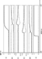
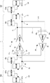
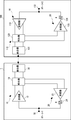
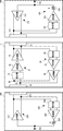
- FIG. It is a block diagram which shows the structure of the communication circuit which concerns on Embodiment 1.
- FIG. It is a circuit diagram which shows the example of the structure of a transmitter. It is a circuit diagram which shows the example of the structure of a receiver. It is a waveform diagram which shows the operation of the communication circuit 1 of Embodiment 1.
- FIG. It is a figure which enlarges a part of FIG. It is a figure which enlarges a part of FIG.
- FIG. It is a block diagram which shows the structure of the communication circuit which concerns on Embodiment 2.
- FIG. It is a waveform diagram which shows the operation of the communication circuit 1 of Embodiment 2. It is a figure which enlarges a part of FIG.
- FIG. It is a figure which enlarges a part of FIG. It is a block diagram which shows the structure of the communication circuit which concerns on Embodiment 3.
- FIG. It is a block diagram which shows the structure of the communication circuit which concerns on Embodiment 4.
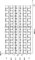
- FIG. It is a figure which shows the layout structure of the transmission line coupler.
- It is a figure which enlarges a part of FIG. It is a figure which enlarges a part of FIG.
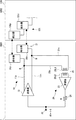
- FIG. 1 is a block diagram showing a configuration of a communication circuit and a communication device according to the first embodiment.
- the communication circuit 1 includes a first substrate SUB 1, a transmission path 10, a reception path 20, couplers 31p and 31n, and a first port 32.
- the transmission path 10 and the reception path 20 are connected in parallel between the coupler 31 and the first port (described as port 1 in the figure) 32.
- the transmission path 10 includes a transmitter 13 and transmission transmission lines 11p and 11n.
- the reception path 20 includes a reception transmission line 21p, 21n, a capacitor 22, a receiver 23, and a resistor 24.
- the configuration between the first port 32 and the transmitter 13 and the configuration between the receiver 23 and the first port 32 are single-ended configurations for transmitting a single-ended (single differential) signal. .. Further, the configuration between the transmitter 13 and the coupler 31 and between the coupler 31 and the receiver 23 is a differential configuration for transmitting a differential signal. Therefore, the first substrate SUB1 is provided with two couplers 31p and 31n. Further, the transmission path 10 from the couplers 31p and 31n to the transmitter 13 is provided with two transmission transmission lines 11p and 11n, and the reception path 20 from the receiver 23 to the couplers 31p and 31n is 2 The reception transmission lines 21p and 21n of the book are provided.
- the coupler 31 may be configured to transmit a single-ended signal instead of a differential signal.
- 0 or 1 digital data is represented by the high and low signal levels with respect to the reference voltage.
- the communication circuit 1 may be provided with one coupler 31.
- the single-ended transmission configuration is used between the first port 32 and the transmitter 13 and between the receiver 23 and the first port 32, a differential transmission configuration may be used. ..
- the communication circuit 1 performs half-duplex communication with the communication circuit 100 which is a communication partner.
- the communication circuit 1 and the communication circuit 100 are communication devices that transmit and receive data by wireless communication.
- the coupler 31 of the communication circuit 1 is a communication coupler and is non-contactly coupled to the coupler 131 of the communication circuit 100. More specifically, the coupler 31p is electromagnetically coupled to the coupler 131p, and the coupler 31n is electromagnetically coupled to the coupler 131n.
- the coupler 31 and the coupler 131 are, for example, the electromagnetic field couplers shown in Patent Documents 1 and 2.
- the coupler 31 and the coupler 131 can be, for example, transmission lines arranged parallel to each other so as to be coupled as a distributed constant system by an electric field and a magnetic field.
- the coupler 31 and the coupler 131 may be overlapping coils (inductive coupling) so as to be magnetically coupled (inductively coupled) as a lumped constant system.
- the coupler 31 and the coupler 131 can be electrodes arranged in parallel with each other so as to be electrically coupled (capacitively coupled) as a lumped constant system.
- the electromagnetic field coupling may be a coupling using at least one of an electric field and a magnetic field.
- a terminating resistor (see FIG. 15) may be connected between the coupler 31p and the coupler 31n.
- the communication circuit 100 includes a second substrate SUB2, a transmission path 110, a reception path 120, a coupler 131, and a second port (described as port 2 in FIG. 1) 132.
- the configuration of the communication circuit 100 is the same as that of the communication circuit 1.
- the transmitter 113 of the transmission path 110 and the transmission transmission line 111 correspond to the transmitter 13 of the transmission path 10 and the transmission transmission line 11, respectively.
- the reception transmission line 121, the capacitor 122, the receiver 123, and the resistor 134 of the reception path 120 correspond to the reception transmission line 21, the capacitor 22, the receiver 23, and the resistor 24 of the reception path 20, respectively.
- the description of the communication circuit 100 will be omitted as appropriate, and the description will focus on the configuration of the communication circuit 1.
- a transmission transmission line 11 and a transmitter 13 are provided between the first port 32 and the coupler 31.
- the transmission transmission line 11 is a wiring formed on the first substrate SUB1 and connects the transmitter 13 and the coupler 31. That is, the transmission data transmitted from the transmitter 13 is transmitted to the coupler 31 via the transmission transmission line 11.
- the reception path 20 is provided with a reception transmission line 21, a capacitor 22, a receiver 23, and a resistor 24.
- the reception transmission line 21 is a wiring formed on the first substrate SUB1 and is provided between the transmitter 13 and the coupler 31.
- the transmission transmission line 11 and the reception transmission line 21 are common between the branch node B and the coupler 31.
- a resistor 24 is provided on the output side of the receiver 23. Although a resistor 24 is provided between the receiver 23 and the first port 32, the resistor 24 may not be provided. That is, the resistance value of the resistor 24 may be 0 ⁇ .
- a capacitor 22 is provided on the input side of the receiver 23. Specifically, the capacitor 22 is arranged in the reception path 20 from the coupler 31 to the receiver 23. A capacitor 22p is provided in the middle of the reception transmission line 21p, and a capacitor 22n is provided in the middle of the reception transmission line 21n. The capacitor 22 is arranged between the branch node B and the receiver 23. The reception transmission line 21 is divided in the middle, and a capacitor 22 is formed at the divided portion.
- the coupler 31 is connected to one electrode of the capacitor 22, and the input terminal of the receiver 23 is connected to the other electrode. In this way, the capacitor 22 is interposed between the input of the receiver 23 and the coupler 31.
- the capacitor 22 can transmit a signal by using electric field coupling (capacitive coupling).
- the transmission path 10 transmits transmission data from the first port 32 to the coupler 31. Then, the communication circuit 1 transmits the transmission data to the communication circuit 100 by utilizing the electromagnetic field coupling between the coupler 31 and the coupler 131. Further, the communication circuit 1 receives the transmission data from the communication circuit 100 by utilizing the electromagnetic field coupling between the coupler 31 and the coupler 131.
- the reception path 20 transmits the received data from the coupler 31 to the receiver 23.
- the receiver 23 restores the received data. Therefore, the received data restored by the receiver 23 is input to the first port 32.
- FIG. 2 shows an example of the circuit configuration of the transmitter 13.
- the transmitter 13 is, for example, a redriver that sets a rising time and a falling time of a signal to predetermined values.
- IN is an input terminal of the transmitter 13
- OUTP and OUTN are differential output terminals.
- FIG. 3 shows an example of the circuit configuration of the receiver 23.
- the receiver 23 has, for example, a hysteresis comparator.
- INP and INN are differential input terminals of the receiver 23, and OUT is an output terminal of the receiver 23.
- a general-purpose semiconductor chip can be used for the receiver 23 and the transmitter 13.
- a commercially available general-purpose chip can be mounted on the first substrate SUB1 as a receiver 23 and a transmitter 13.
- FIGS. 4 to 6 are diagrams showing signal waveforms obtained by circuit simulation.
- FIG. 5 shows an enlarged view of 398 ns to 405 ns in FIG. 4
- FIG. 6 shows an enlarged view of 500 s to 507 ns in FIG.
- the communication circuit 1 transmits a signal to the communication circuit 100
- 500 ns and 900 ns the communication circuit 1 receives the signal from the communication circuit 100.
- the waveform V1 indicates the potential of the first port 32 (see FIG. 1).
- the waveform VO1 indicates the potential of the node on the output side of the transmitter 13 (see VO1P and VO1N in FIG. 1).
- VI1 indicates the potential of the node on the input side of the receiver 23 (see VI1P and VI1N in FIG. 1).
- the waveform VO1 shows the signal waveform from the transmitter 13 to the coupler 31, and the waveform VI1 shows the signal waveform from the capacitor 22 to the receiver 23. Further, because of the differential configuration, the waveform VO1P shows the potential on the coupler 31p side, and the waveform VO1N shows the potential on the coupler 31n side.
- the waveform VI1P shows the potential on the capacitor 22p side
- the waveform VI1N shows the potential on the capacitor 22n side.
- VO1P and VO1N are collectively shown as VO1
- VI1P and VI1N are collectively shown as VI1.
- VO1P and VI1P are shown by a solid line
- VO1N and VI1N are shown by a broken line.
- the waveforms V2, VI2, and VO2 indicate the potentials on the SUB2 side of the second substrate, and correspond to V1, VI1, and VO1, respectively. That is, the waveform V2 shows the potential of the second port 132.
- the waveform VI2 indicates the potential on the input side of the receiver 123, and the VO2 indicates the potential on the output side of the transmitter 113.
- the waveform VI2 shows the waveforms VI2P and VI2N having a differential configuration
- the waveform VO2 shows the waveforms VI2P and VI2N having a differential configuration.
- R the resistance value of the resistor 24. If R is too small, it becomes difficult to input a digital signal to the first port 32. That is, when the receiver 23 outputs 0 and the circuit for driving the first port 32 (a drive circuit (not shown) connected to the upstream side of the first port 32) outputs 1, it drives the first port 32. A current flows from the circuit to the output of the receiver 23 via the resistor 24. If the resistance value R is sufficiently large, the potential of the first port 32 approaches high sufficiently, but if the resistance value R is too small, the potential of the first port 32 drops significantly. On the other hand, the larger the resistance value R, the longer the drive time of the output of the receiver 23, and the higher the signal transfer becomes impossible.
- the resistance value R is typically 500 ⁇ , which is 10 times that. In the simulations of FIGS. 4 to 6, the resistance value R is set to 10 ⁇ so that the effect when the resistance value R is small can be seen. Further, the capacitance value of the capacitor 22 is 10 pF, and the transmission rate is 20 Mbps.
- a small-amplitude reception pulse with positive polarity is generated in the coupler 131 (G in FIG. 5).
- This received pulse is input to the receiver 123 via the capacitor 122 (H in FIG. 5). Therefore, the hysteresis comparator of the receiver 123 restores the received pulse to 1 of the digital signal (I in FIG. 5). In this way, the digital signal input to the first port 32 is transferred to the second port 132.
- the change in the output of the transmitter 13 is input to the receiver 23 via the capacitor 22.
- the output of the receiver 23 changes to 1.
- the above-mentioned collision between the circuit for driving the first port 32 and the output of the receiver 23 is eliminated (J in FIG. 5). Since 1 has already been input to the first port 32, even if the receiver 23 outputs 1, the transmitter 13 does not transmit 1 again (K in FIG. 5). In other words, for example, you will hear the words you spoke a little later, but you will not speak the same words more than once.
- the receiver 23 on the first port 32 side has already completed the reception of 1, the receiver 23 does not receive 1 again due to this. That is, for example, the signal transmitted by the first port 32 returns from the second port 132 like Yamabiko, but both the receiver 23 of the first port 32 and the receiver 123 of the second port 132 have already received 1. I'm done.
- the capacitance value C of the capacitor 22 there is a restriction on the range of the size of the capacitance value C of the capacitor 22.
- the smaller the capacitance value C the smaller the amplitude of the received pulse input to the receiver 23. If the capacitance value C is too small, the receiver 23 cannot receive the signal.
- the larger the capacitance value C the longer the time for the input potential of the receiver to return to the original potential after transfer (the time for preparing to receive the next signal of the opposite polarity). For this reason, the communication circuit 1 cannot receive data at high speed.
- the time constant obtained by multiplying 50 ⁇ by the capacitance value C is about 50% of the cycle time (50 ps). For some reason, the capacitance value C is about 80 pF. According to the circuit simulation, the capacitance value C enables bidirectional communication at 20 Mbps in the range of 1 pF to 60 pF. Further, when the capacitance value C is 1 pF, bidirectional communication of up to 480 Mbps is possible.
- the circuit operation when the digital signal input to the first port 32 changes from 1 to 0 is the same as above.
- the digital signal input to the first port 32 is transferred to the second port 132 side via the coupler 31. This digital signal is simultaneously received at the first port 32 and the second port 132 via the electric field coupling of the capacitor 22.
- the first port 32 receives the digital signal transmitted by the first port 32 itself again.
- the second port 132 transmits the digital signal received from the first port 32 to the first port 32. Therefore, the same signal is returned from the second port 132 to the first port 32 like Yamabiko with a little delay from the first transmission of the receiver 23.
- the receivers 23 and 123 of the first port 32 and the second port 132 have already received the signal. Therefore, the receivers 23 and 123 are ready to hear the opposite signal next. That is, since the threshold value is changed by the hysteresis comparator, the same signal does not reverberate (reciprocate) any more.
- the circuit of FIG. 1 has a symmetrical configuration on the first port 32 side and the second port 132 side with the couplers 31 and 131 interposed therebetween. Therefore, even if the signal transfer directions are opposite, the circuit operations on the transmitting side and the receiving side are the same as those described above. That is, when the second port 132 transmits a signal, the first port 32 receives the signal.
- V2, VI2, and VO2 in FIG. 6 have the same signal waveforms as V1, VI1, and Vo1 in FIG. 5, respectively.
- V1, VI1, and VO1 in FIG. 6 have the same signal waveforms as V2, VI2, and VO2 in FIG. 5, respectively. Therefore, detailed description will be omitted.
- the transmission signal output from the transmitter 13 is input to the receiver 23 via the electric field coupling of the capacitor 22.
- the transmitter 13 and the receiver 23 make positive feedback. That is, the input of the transmitter 13 and the output of the receiver 23 are signals having the same polarity, and the output of the transmitter 13 and the input of the receiver 23 converge to the same polarity. Further, the transmitter 113 and the receiver 123 return positively. That is, the input of the transmitter 113 and the output of the receiver 123 are signals having the same polarity, and the output of the transmitter 113 and the input of the receiver 123 converge to the same polarity.
- half-duplex communication can be realized with a simple configuration.
- Half-duplex communication can be realized without obtaining a timing signal for switching transmission / reception (that is, asynchronously).
- Commercially available chips can be used for the transmitter 13 and the receiver 23, respectively.
- the communication circuit 1 can be realized by combining a commercially available chip and a capacitor 22 as a passive element. Therefore, the development cost can be suppressed. As a result, a highly practical communication circuit 1 can be realized.
- FIG. 7 is a block diagram showing the configuration of the communication circuit 1.
- the positions of the capacitors are different.
- the configuration other than the position of the capacitor is the same as that of the first embodiment, and thus the description thereof will be omitted.
- the capacitor 12 is arranged in the transmission path 10 between the transmitter 13 and the coupler 31.
- the capacitor 12 is arranged between the output side of the transmitter 13 and the branch node B. Therefore, the capacitor 12 is interposed in the middle of the transmission transmission line 11. Even in such a configuration, the same effect as that of the first embodiment can be obtained.
- FIGS. 8 to 10 are diagrams showing signal waveforms obtained by circuit simulation.
- 9 shows an enlarged view of 398 ns to 405 ns in FIG. 8
- FIG. 10 shows an enlarged view of 500 s to 507 ns in FIG.
- the communication circuit 1 transmits a signal to the communication circuit 100
- 500 ns and 900 ns the communication circuit 1 receives the signal from the communication circuit 100.
- the capacitor 12 is connected to the output of the transmitter 13 instead of the input of the receiver 23.
- a digital signal is input from the transmitter 13 to the other receiver 123 via the couplers 31, 131, the capacitor 122, and the capacitor 22.
- a digital signal is input from the transmitter 13 to the other receiver 123 via the capacitor 12, the couplers 31, 131, and the capacitor 122. Therefore, the circuit operation of the communication circuit 1 of the second embodiment is substantially the same as that of the communication circuit 1 of the first embodiment. Therefore, the signal waveforms of FIGS. 8 to 10 are the same as those of FIGS. 4 to 6.
- a circuit for setting the common mode of the input signal of the receiver 23 to a receivable potential is required on the receiver 23 side.
- Vb in FIG. 3 is a circuit for setting the potential.
- the transmitter 13 and the receiver 23 make positive feedback.
- half-duplex communication can be realized with a simple configuration.
- Half-duplex communication can be realized without obtaining a timing signal for switching transmission / reception (that is, asynchronously).
- the communication circuit 1 can be realized by combining a commercially available chip (for example, a transmitter 13 or a receiver 23) with a capacitor 12 as a passive element. Therefore, the development cost can be suppressed. As a result, a highly practical communication circuit 1 can be realized.
- Embodiment 3 The communication circuit 1 of the third embodiment will be described with reference to FIG.
- FIG. 11 is a block diagram showing the configuration of the communication circuit 1.
- the capacitor 22 of the first embodiment has been replaced by the transformer 25. Since the configurations other than the transformer 25 are the same as those in the first embodiment, detailed description thereof will be omitted.
- the configuration of the communication circuit 100 is the same as that of the communication circuit 1, the configurations other than the coupler 131 on the communication circuit 100 side are omitted.
- the transformer 25 has a primary inductance 25L1 and a secondary inductance 25L2.
- the primary inductance 25L1 and the secondary inductance 25L2 are coils, respectively, and are arranged in parallel with each other.
- the two inductances 25L1 and 25L2 of the transformer 25 are non-contact and magnetically coupled (inductively coupled). Since the transformer 25 can transfer the change in the signal by using the magnetic field coupling, the circuit operation is the same as that in the first embodiment.
- the transmitter 13 and the receiver 23 make positive feedback.
- half-duplex communication can be realized with a simple configuration.
- Half-duplex communication can be realized without obtaining a timing signal for switching transmission / reception (that is, asynchronously).
- the communication circuit 1 can be realized by combining a commercially available chip (for example, a transmitter 13 or a receiver 23) with a transformer 25 as a passive element. Therefore, the development cost can be suppressed. As a result, a highly practical communication circuit 1 can be realized.
- the transformer 25 is arranged on the input side of the receiver 23 in FIG. 11, the transformer 25 may be arranged on the output side of the receiver 23 as in the capacitor 12 of the second embodiment. The same effect can be obtained by this configuration.
- the transformer 25 may be arranged on the transmission transmission line 11 instead of the reception transmission line 21. That is, the transformer 25 may be arranged instead of the capacitor 12 of FIG.
- FIG. 12 is a block diagram showing the configuration of the communication circuit 1 of the fourth embodiment.
- the capacitor 22 of the first embodiment is replaced with the transmission line coupler 26 and the transmission line coupler 27. Since the configurations other than the transmission line couplers 26 and 27 are the same as those in the first embodiment, the description thereof will be omitted.
- the configuration of the communication circuit 100 is the same as that of the communication circuit 1, the configurations other than the coupler 131 on the communication circuit 100 side are omitted.
- the transmission line couplers 26 and 27 are composed of transmission lines (wiring patterns) formed on the first substrate SUB1.
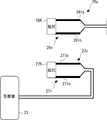
- the detailed configuration of the transmission line couplers 26 and 27 is shown in FIG. FIG. 13 is a diagram showing the layout of the transmission line couplers 26 and 27 on the first substrate SUB1.
- the differential pair of the transmission line coupler 26 is referred to as a transmission line coupler 26p, 26n.
- the differential pair of the transmission line coupler 27 is a transmission line coupler 27p, 27n.
- the transmission line coupler 26p has a first transmission line 261p, and the transmission line coupler 26n has a first transmission line 261n.
- the first transmission line 261p and the first transmission line 261n are collectively referred to as the first transmission line 261.
- the transmission line coupler 27p has a second transmission line 271p, and the transmission line coupler 27n has a second transmission line 271n.
- the second transmission line 271p and the second transmission line 271n are collectively referred to as the second transmission line 271.
- the first transmission line 261p, the first transmission line 261n, the second transmission line 271p, and the second transmission line 271n are transmission lines (wiring patterns) formed on the same first substrate SUB1.
- the transmission line couplers 26 and 27 the coupler having the configuration shown in FIG. 33 of Patent Document 1 or FIG. 2 of Patent Document 2 can be used.
- the first transmission line 261p and the first transmission line 261n are a differential transmission line pair and are connected to the coupler 31.
- One end of the first transmission line 261p is connected to the coupler 31p, and one end of the first transmission line 261n is connected to the coupler 31n.
- the other end of the first transmission line 261p is connected to the resistor 26R, and the other end of the first transmission line 261n is connected to the resistor 26R.
- the first transmission line 261p and the first transmission line 261n are connected via a resistor 26R.
- the resistor 26R is a terminating resistor that terminates the first transmission line 261p and the first transmission line 261n.
- the second transmission line 271p and the second transmission line 271n are a differential transmission line pair and are connected to the input side of the receiver 23.
- One end of the second transmission line 271p is connected to the input terminal of the positive electrode of the receiver 23, and one end of the second transmission line 271n is connected to the input terminal of the negative electrode of the receiver 23.
- the other end of the second transmission line 271n is connected to the resistor 27R, and the other end of the second transmission line 271n is connected to the resistor 27R.
- the second transmission line 271p and the second transmission line 271n are connected via a resistor 27R.
- the resistor 27R is a terminating resistor that terminates the second transmission line 271p and the second transmission line 271n.
- the first transmission line 261p and the second transmission line 271p are electromagnetically coupled.
- the first transmission line 261p and the second transmission line 271p transmit the differential signal of the positive electrode by electromagnetic field coupling.
- the first transmission line 261p and the second transmission line 271p are arranged so as to face each other via an insulator.
- the first transmission line 261p and the second transmission line 271p may be formed of different wiring layers or may be formed of the same wiring layer.
- the first transmission line 261p and the second transmission line 271p are formed of different wiring layers, the first transmission line 261p and the second transmission line 271p are arranged in a plan view orthogonal to the thickness direction of the first substrate SUB1. Are arranged so as to overlap with each other via an insulating layer.
- the first transmission line 261p and the second transmission line 271p are formed of the same wiring layer, the first transmission line 261p and the second transmission line 271p are arranged in parallel in close proximity to each other in a plan view.
- the first transmission line 261n and the second transmission line 271n are electromagnetically coupled in the same manner as the first transmission line 261p and the second transmission line 271p.
- the first transmission line 261n and the second transmission line 271n transmit the differential signal of the negative electrode by electromagnetic field coupling.
- the first transmission line 261n and the second transmission line 271n are arranged so as to face each other via an insulator, similarly to the first transmission line 261p and the second transmission line 271p.
- Two transmission lines (wiring patterns) formed in parallel with the first transmission line 261n and the second transmission line 271n and arranged in close proximity to each other.
- the first transmission line 261n and the second transmission line 271n may be formed of different wiring layers or may be formed of the same wiring layer.
- the first transmission line 261n and the second transmission line 271n are formed of different wiring layers, the first transmission line 261n and the second transmission line 271n are arranged so as to overlap each other via an insulating layer in a plan view. Will be done.
- the first transmission line 261n and the second transmission line 271n are formed of the same wiring layer, the first transmission line 261n and the second transmission line 271n are arranged in parallel in close proximity to each other in a plan view.
- half-duplex communication can be realized with a simple configuration.
- Half-duplex communication can be realized without obtaining a timing signal for switching transmission / reception (that is, asynchronously).
- the communication circuit 1 can be realized by combining a commercially available chip (for example, a transmitter 13 or a receiver 23) and a transmission line as a passive element (first transmission line 261p, 261n, second transmission line 271p, 271n). Therefore, the development cost can be suppressed. As a result, a highly practical communication circuit 1 can be realized.
- Embodiment 5 The communication circuit 1 of the fifth embodiment will be described with reference to FIG. FIG. 14 is a block diagram showing the configuration of the communication circuit 1 of the fifth embodiment.
- the transmission line couplers 26p, 26n, 27p, 27n formed on the same first substrate SUB1 are used.
- the branch node B is provided in the transmission transmission line 11, whereas in the fifth embodiment, the signal is branched by the transmission line coupler. That is, since there is no branch node B on the first substrate SUB1, signal reflection can be reduced.
- the communication operation is the same as that of the first embodiment, but since the signal is branched by the transmission line couplers 26 and 27 instead of the capacitor 22, the input common mode potential of the receiver 23 quickly becomes the original potential after receiving the signal. You can go back to. Therefore, according to the configuration of the present embodiment, data can be transferred at high speed.
- the configuration of the communication circuit 100 is the same as that of the communication circuit 1.
- the transmission line couplers 126p, 126n, 127p, 127n correspond to the transmission line couplers 26p, 26n, 27p, and 27n, respectively. Therefore, the description of the communication circuit 100 will be omitted.
- FIG. 15 is a diagram showing the layout of the transmission line couplers 26 and 27 on the first substrate SUB1.
- One end of the first transmission line 261p is connected to the output of the transmitter 13, and the other end is connected to the coupler 31p. That is, the transmitter 13 and the coupler 31p are connected via the first transmission line 261p.
- One end of the first transmission line 261n is connected to the output of the transmitter 13, and the other end is connected to the coupler 31n.
- the coupler 31p and the coupler 31n are terminated by a terminating resistor 31R. That is, the transmitter 13 and the coupler 31n are connected via the first transmission line 261n.
- the second transmission lines 271p and 271n are connected to the input of the receiver 23 as in the fourth embodiment.
- the first transmission line 261p and the second transmission line 271p are electromagnetically coupled.
- the first transmission line 261p and the second transmission line 271p are formed of different wiring layers and overlap each other via an insulating film.
- the first transmission line 261p and the second transmission line 271p may be formed of the same wiring layer.
- the first transmission line 261n and the second transmission line 271n are electromagnetically coupled.
- the first transmission line 261n and the second transmission line 271n are formed of different wiring layers and overlap each other via an insulating film.
- the first transmission line 261n and the second transmission line 271n may be formed of the same wiring layer.
- the received signal received by the coupler 31 is input to the receiver 23 by the electromagnetic field coupling between the transmission line coupler 26 and the transmission line coupler 27. Further, the transmission signal from the transmitter 13 is input to the coupler 31 via the transmission line coupler 26.
- the transmission signal is transmitted to the communication circuit 100 by the electromagnetic field coupling of the coupler 31 and the coupler 131.
- the receiver 123 of the communication circuit 100 restores the transmitted signal.
- the second port 132 of the communication circuit 100 receives the transmission signal.
- the transmission signal received by the second port 132 is transmitted to the coupler 131 via the transmitter 113 and the transmission line coupler 126 on the second board SUB2.
- the transmission signal is transmitted to the communication circuit 1 by the electromagnetic field coupling of the coupler 131 and the coupler 31.
- the transmission signal returned to the communication circuit 1 is input to the receiver 23 by the electromagnetic field coupling between the transmission line coupler 26 and the transmission line coupler 27. That is, the transmission signal transmitted from the communication circuit 1 to the communication circuit 100 returns from the communication circuit 100 to the communication circuit 1.
- the coupling coefficient of the transmission line coupler 26 and the transmission line coupler 27 is k
- the coupling coefficient of the transmission line coupler 126 and the transmission line coupler 127 is k
- the coupling coefficient of the coupler 31 and the coupler 131 is k0.
- FIGS. 16 to 18 are diagrams showing signal waveforms obtained by circuit simulation.
- FIG. 17 shows enlarged 398 ns to 405 ns in FIG. 16, and
- FIG. 18 shows enlarged 500 s to 507 ns in FIG.
- the communication circuit 1 transmits a signal to the communication circuit 100, and after 500 ns, the communication circuit 1 receives the signal from the communication circuit 100.
- the signal waveforms of VTL1 and VTL2 are added.
- VTL1 indicates the potential of the node between the coupler 31 and the transmission line coupler 26
- VTL2 indicates the potential of the node between the coupler 131 and the transmission line coupler 126.
- the waveforms VTL1P and VTL2P of the differential signal on the positive electrode side are shown by solid lines, and the waveforms VTL1N and VTL2N of the differential signals on the negative electrode side are shown by broken lines.
- half-duplex communication can be realized with a simple configuration.
- Half-duplex communication can be realized without obtaining a timing signal for switching transmission / reception (that is, asynchronously). Further, since there is no branch node B in the transmission path 10 and the reception path 20, signal reflection can be suppressed.
- Embodiment 6 The communication circuit 1 of the sixth embodiment will be described with reference to FIG.
- FIG. 19 is a block diagram showing the configuration of the communication circuit 1 of the present embodiment.
- the arrangement of the receiver 23 and the transmitter 13 of the fifth embodiment is exchanged.
- the transmission line coupler 26p has a transmission line arranged between the coupler 31p and the receiver 23.
- the transmission line coupler 26n has a transmission line arranged between the coupler 31n and the receiver 23.
- the transmission line couplers 27p and 27n are connected to the output side of the transmitter 13. Also in this configuration, the same operation as that of the communication circuit 1 of the fifth embodiment can be performed.
- Half-duplex communication can be realized with a simple configuration.
- Half-duplex communication can be realized without obtaining a timing signal for switching transmission / reception (that is, asynchronously). Further, since there is no branch node B in the transmission path 10 and the reception path 20, signal reflection can be suppressed.
- Embodiment 7 The communication circuit 1 according to the present embodiment will be described with reference to FIG.
- FIG. 20 is a block diagram showing the configuration of the communication circuit 1 of the present embodiment.
- the communication circuit 1 is a repeater that relays signals.
- the communication circuit 1 relays the signal from the communication circuit 300 and transmits it to the communication circuit 100. Further, the communication circuit 1 relays the signal from the communication circuit 100 and transmits it to the communication circuit 300. As described above, the communication circuit 1 is a bidirectional repeater.
- the communication circuit 100 and the communication circuit 300 have the same configuration as the communication circuit 100 shown in the first embodiment, the description thereof will be omitted.
- the communication circuit 100 and the communication circuit 300 may be repeaters having the same configuration as the communication circuit 1 according to the present embodiment. In this case, the signal can be relayed twice or more.
- the capacitor 12, the receiver 18, and the transmitter 28 are added to the communication circuit 1 of the first embodiment. Further, couplers 35p and 35n (hereinafter, collectively referred to as coupler 35) have been added. Further, the resistor 24 is omitted from the communication circuit 1 of the first embodiment. The description of the same configuration as that of the first embodiment will be omitted as appropriate.
- the coupler 35 is an electromagnetic field coupler similar to the coupler 31.
- the coupler 35 is electromagnetically coupled to the coupler 331 of the communication circuit 300 of the communication partner.
- a capacitor 12, a receiver 18, and a transmitter 13 are connected in series in this order to the transmission path 10 from the coupler 35 to the coupler 31. Therefore, the transmitter 13 is arranged between the receiver 18 and the coupler 35.
- the transmitter 13 outputs the signal restored by the receiver 18 to the coupler 31.
- a capacitor 12 is arranged between the receiver 18 and the coupler 31.
- a first port 32 is provided between the capacitor 12 and the coupler 35. That is, the coupler 35 is connected to the first port 32.
- the capacitor 22, the receiver 23, and the transmitter 28 are connected in series in this order to the receiving path 20 from the coupler 31 to the coupler 35. Therefore, the capacitor 22 is arranged between the receiver 23 and the coupler 35.
- a transmitter 28 is arranged between the receiver 23 and the coupler 31. The transmitter 28 outputs the signal restored by the receiver 23 to the coupler 35.
- the first to seventh embodiments can be combined as appropriate.
- the transformer 25 may be used instead of the capacitors 22 and 12, and the transmission line coupler 26 and the transmission line coupler 27 may be used.
- the first communication coupler that electromagnetically couples with the coupling of the communication partner and the transmission data transmitted from the first communication coupling are input.
- a first port for outputting received data received by the first communication coupler, a transmission path for transmitting the transmission data from the first port to the first communication coupler, and the first.
- the communication method by the communication circuit 1 includes a step in which the transmitter outputs the transmission data input to the first port as a transmission signal and an electromagnetic field coupling of the transmission signal output from the transmitter in a transmission coupler. It is provided with a step of inputting to the receiver via.
- the communication circuit 1 is a transmission coupler arranged in the transmission path between the first coupler and the transmitter, or in the reception path from the first coupler to the receiver. It is provided with the transmission coupler for transmitting the transmission data or the reception data by electromagnetic field coupling.
- FIGS. 21 to 25 Examples of arrangement of the transmission coupler are shown in FIGS. 21 to 25.
- the coupler 31 is the first communication coupler.
- the transmission coupler 29 is arranged in the reception path 20 between the coupler 31 and the receiver 23.
- the transmission coupler 19 is arranged in the transmission path 10 between the coupler 31 and the transmitter 13. 21 corresponds to the first or third embodiment, and FIG. 22 corresponds to the second embodiment. Therefore, detailed description thereof will be omitted.
- the transmission couplers 19 and 29 have a passive element such as the capacitor 22 of the first, second, and seventh embodiments, or the transformer 25 of the third embodiment.
- the transmission couplers 19 and 29 have passive elements such as the first transmission line 261 and the second transmission line 271, as in the fourth to sixth embodiments.
- FIGS. 23 and 24 show an arrangement example in which the transmission couplers 19 and 29 form a branch.
- the transmission coupler 29 corresponds to the transmission line couplers 26 and 27 of the fifth and sixth embodiments.
- FIG. 23 corresponds to the sixth embodiment, and
- FIG. 24 corresponds to the fifth embodiment. Since the basic configurations of FIGS. 23 and 24 are the same as those of the fifth and sixth embodiments, the description thereof will be omitted.
- the transmission coupler 19 has a transmission line coupler 26 and a transmission line coupler 27 as shown in FIG. Then, the first transmission line 261 connects the transmitter 13 to the coupler 31.
- the second transmission line 271 is connected to the receiver 23.
- the transmission coupler 29 has a transmission line coupler 26 and a transmission line coupler 27.
- the first transmission line 261 connects the receiver 23 to the coupler 31.
- the second transmission line 271 is connected to the transmitter 13.
- the communication circuit 1 is a repeater. That is, the communication circuit 1 relays the data communication between the communication circuit 100 and the communication circuit 300.
- a transmission coupler 129 is arranged in the reception path 120 between the receiver 123 and the coupler 131.
- a transmission coupler 329 is arranged in the reception path 320 between the receiver 323 and the coupler 331.
- the transmission coupler 129 may be arranged in the transmission path 110 between the coupler 131 and the transmitter 113 as in the second embodiment.
- the transmission coupler 329 may be arranged in the transmission path 310 between the coupler 331 and the transmitter 313 as in the second embodiment.
- the transmission data from the third port 332 is transmitted to the second port 132 via the communication circuit 1 serving as the relay board. Since the basic configuration of FIG. 25 is the same as the above, the description thereof will be omitted.
- the transmission coupler 29, 129, 329 shown in FIG. 25 has a passive element such as the capacitor 22 of the first, second, and seventh embodiments, or the transformer 25 of the third embodiment.
- the transmission couplers 29, 129, and 329 have passive elements such as the first transmission line 261 and the second transmission line 271, as in embodiments 4-6.
- half-duplex communication can be performed without using a timing signal.
- the resistance values of the resistors 24, 124, and 324 in FIGS. 21 to 25 may be 0 ⁇ . That is, the resistors 24, 124, 324 can be omitted.
Landscapes
- Engineering & Computer Science (AREA)
- Computer Networks & Wireless Communication (AREA)
- Signal Processing (AREA)
- Near-Field Transmission Systems (AREA)
- Dc Digital Transmission (AREA)
Abstract
タイミング信号を用いずとも、半二重通信を行なうことができる通信回路、及び通信方法を提供する。 本実施形態に係る通信回路(1)は、結合器(31)と、第1ポート(32)と、第1ポートから結合器(31)に送信データを伝送する送信経路(10)と、結合器(31)から前記第1ポート(32)に受信データを伝送する受信経路(20)と、送信経路(10)に配置された送信器(13)と、受信経路(20)に配置された受信器(23)と、結合器(31)から送信器(13)までの間の送信経路(10)、又は結合器(31)からの受信器(23)までの受信経路(20)に配置された受動素子を有する伝送用結合器(29)であって、送信データ又は受信データを電磁界結合により伝送する伝送用結合器(29)と、を備えている。
Description
本発明は電磁界結合を用いた通信回路、及び通信方法に関し、特に詳しくは、送受信を切り替えるタイミング信号を用いずに、半二重通信を行なうことができる通信回路、及び通信方法に関する。
半二重通信とは、2つのモジュールの間で時分割に双方向に通信することである。具体的には、半二重通信とは、一方のモジュールが送信で他方のモジュールが受信となるように時間で切り替える方式である。コンピュータと周辺機器を接続するUSB(Universal Serial Bus)やコンピュータとディスプレイを接続するHDMI(登録商標)(High Definition Multimedia Interface)では、半二重通信が用いられている。例えば、2つの機器間で、相互認証を行ったり、暗号化されたデータやスクランブルのかかった映像データを復元する鍵をやり取りしている。
USBやHDMIで機器を接続する際にコネクタが用いられる。一般的な圧着接続のコネクタでは、信号が反射して高速通信できない、機器を小型化できないなどの課題がある。こうしたコネクタの課題を解決するために、本出願の発明者は、デジタルデータを無線通信する非接触コネクタを提案している(例えば特許文献1、2参照)。
特許文献1のモジュール間通信装置では、プリント回路基板(Printed Circuit Board;PCB)に伝送線路が形成されている。積層方向から見て、2つプリント回路基板の伝送線路が投影的に重なるように配置されている。このようにすることで、2つの伝送線路の間に容量結合及び/又は誘導結合を形成することができる。容量結合及び/又は誘導結合による結合器(以下、電磁界結合器とする)を介して、信号が送受信される。受信器は、ヒステリシス比較器を用いて、結合器を介して伝送された受信信号を、元の信号に復元する(段落0191)。
特許文献2では、結合器を差動構成とするために、結合器に一対の入出力接続線が接続された構成が開示されている(図2)。
また、特許文献3では双方向性バス・バッファが開示されている。特許文献3の双方向性バス・バッファでは、両ポートにデジタル信号が入力されている。そして、タイミングを制御する制御信号が用いられている。
電磁界結合器を介して受信されたデジタル信号は、DC成分が失われて、小振幅のパルス信号となる。小振幅のパルス信号をデジタル信号に復元する受信回路は、デジタル信号を送信する送信回路と接続して同時に用いることはできない。なぜなら、デジタル信号の振幅が受信信号に比べて大きいために、送信回路が出力しているデジタル信号を出力しているときに、小振幅のパルス信号を受信しても、受信回路がそれを検出できないからである。
半二重通信において用いられる送受信を切り替えるタイミング信号を用いれば、受信時において、送信回路の出力をHigh-Z(ハイインピーダンス)にすることができるため、受信回路が受信信号を検出することができる。しかし、そのようなタイミング信号を、伝送線路の途中のコネクタにおいて抽出することは、一般に困難である。したがって、本実施形態は、送受信を切り替えるタイミング信号を得ずとも(すなわち非同期に)半二重通信を可能にすることを目的とする。
本実施の形態に係る通信回路は、通信相手の結合器と電磁界結合する第1の通信用結合器と、前記第1の通信用結合器から送信される送信データが入力されるとともに、前記第1の通信用結合器が受信した受信データを出力する第1ポートと、前記第1ポートから前記第1の通信用結合器に前記送信データを伝送する送信経路と、前記第1の通信用結合器から前記第1ポートに前記受信データを伝送する受信経路と、前記送信経路に配置され、前記第1ポートからの前記送信データを前記第1の通信用結合器に出力する送信器と、前記受信経路に配置され、前記第1の通信用結合器を介して受信した前記受信データを復元する受信器と、前記第1の通信用結合器から前記送信器までの間の前記送信経路、又は前記第1の通信用結合器からの前記受信器までの前記受信経路に配置された受動素子を有する伝送用結合器であって、前記送信データ又は前記受信データを電磁界結合により伝送する前記伝送用結合器と、を備えている。
上記の通信回路において、前記受動素子がキャパシタを有していてもよい。
上記の通信回路において、前記受動素子がトランスを有していてもよい。
上記の通信回路において、前記受動素子が、基板上に形成された第1伝送線路と前記基板上に形成され、前記第1伝送線路と電磁界結合した第2伝送線路と、を有していていてもよい、
上記の通信回路において、前記第1伝送線路が、前記受信器又は前記送信器を前記第1の通信用結合器に接続していていてもよい。
上記の通信回路において、前記第1ポートに接続された第2の通信用結合器をさらに備え、前記第2の通信用結合器で受信したデータが、前記送信データとして、前記送信経路を介して、前記第1の通信用結合器に伝送され、前記第1の通信用結合器で受信したデータが、前記受信データとして、前記受信経路を介して、前記第2の通信用結合器に伝送されていてもよい。
本実施の形態にかかる通信方法は、通信相手の結合器と電磁界結合する第1の通信用結合器と、前記第1の通信用結合器から送信される送信データが入力されるとともに、前記第1の通信用結合器が受信した受信データを出力する第1ポートと、前記第1ポートから前記第1の通信用結合器に前記送信データを伝送する送信経路と、前記第1の通信用結合器から前記第1ポートに前記受信データを伝送する受信経路と、前記送信経路に配置され、前記第1ポートからの前記送信データを前記第1の通信用結合器に出力する送信器と、前記受信経路に配置され、前記第1の通信用結合器を介して受信した前記受信データを復元する受信器と、を備えた通信回路による通信方法であって、前記第1ポートに入力された前記送信データを前記送信器が送信信号として出力するステップと、前記送信器から出力された送信信号を伝送用結合器の電磁界結合を介して、前記受信器に入力するステップとを備えている。
本実施の形態にかかる通信回路、及び通信方法によれば、送受信を切り替えるタイミング信号を用いずとも、半二重通信を行なうことができる。
実施の形態1.
以下、図面を参照して本発明の実施の形態について説明する。図1は、本実施の形態1にかかる通信回路及び通信装置の構成を示すブロック図である。図1に示すように、通信回路1は、第1基板SUB1と、送信経路10と、受信経路20と、結合器31p、31nと、第1ポート32と、を備えている。送信経路10と受信経路20とは、結合器31と第1ポート(図ではポート1と記載)32との間に並列に接続されている。
以下、図面を参照して本発明の実施の形態について説明する。図1は、本実施の形態1にかかる通信回路及び通信装置の構成を示すブロック図である。図1に示すように、通信回路1は、第1基板SUB1と、送信経路10と、受信経路20と、結合器31p、31nと、第1ポート32と、を備えている。送信経路10と受信経路20とは、結合器31と第1ポート(図ではポート1と記載)32との間に並列に接続されている。
送信経路10は、送信器13、及び送信伝送路11p、11nを備えている。受信経路20は、受信伝送路21p、21n、キャパシタ22、受信器23、及び抵抗24を備えている。
なお、第1ポート32から送信器13までの間の構成、及び受信器23から第1ポート32までの間の構成が、シングルエンド(片差動)信号を伝送するシングルエンド構成となっている。また、送信器13から結合器31までの間、結合器31から受信器23までの間の構成が、差動信号を伝送する差動構成となっている。したがって、第1基板SUB1には、2つの結合器31p、31nが設けられている。また、結合器31p、31nから送信器13までの送信経路10には、2本の送信伝送路11p、11nが設けられ、受信器23から結合器31p、31nまでの受信経路20には、2本の受信伝送路21p、21nが設けられている。
差動信号を伝送する2つの構成要素(差動対)を識別する場合、p、又はnの添え字を付して説明する。差動信号を伝送する2つの構成要素を特に区別しない場合は、p、及びnの添え字を付さずに説明する。例えば、2本の送信伝送路11p、11nを識別する場合、送信伝送路11p、11nとし、識別しない場合、送信伝送路11とする。同様に、2本の受信伝送路21p、21nを識別する場合、受信伝送路21p、21nとし、識別しない場合、受信伝送路21とする。また、キャパシタ22p、22n等の他の構成要素についても同様に記載する。
なお、結合器31が、差動信号ではなく、シングルエンド信号を伝送する構成であってもよい。シングルエンド伝送の場合、基準電圧に対する信号レベルの高低で0又は1のデジタルデータが表現される。この場合、通信回路1には、1つの結合器31が設けられていればよい。また、第1ポート32から送信器13までの間、及び受信器23から第1ポート32までの間は、シングルエンド伝送の構成となっているが、差動伝送の構成となっていてもよい。
通信回路1は、通信相手となる通信回路100との間で、半二重通信を行なう。通信回路1及び通信回路100は、無線通信によりデータを送受信する通信装置となる。具体的には、通信回路1の結合器31は、通信用結合器であり、通信回路100の結合器131と非接触で結合している。より詳細には、結合器31pが結合器131pと電磁界結合し、結合器31nが結合器131nと電磁界結合する。
結合器31、及び結合器131は、例えば、特許文献1、2に示した電磁界結合器である。結合器31、及び結合器131は、例えば、電界および磁界で分布定数系として結合するように互い平行に配置された伝送線路とすることができる。あるいは、結合器31、及び結合器131は、集中定数系として磁界結合(誘導結合)するように、重複配置されたコイル(誘導結合器)とすることができる。あるいは、結合器31、及び結合器131は、集中定数系として電界結合(容量結合)するように、互い平行に配置された電極とすることができる。電磁界結合とは、電界及び磁界の少なくとも一方を用いた結合であればよい。なお、結合器31pと結合器31nとの間に、終端抵抗(図15参照)が接続されていてもよい。
通信回路100は、第2基板SUB2と、送信経路110と、受信経路120と、結合器131と、第2ポート(図1ではポート2と記載)132と、を備えている。なお、通信回路100の構成は、通信回路1と同様の構成となっている。例えば、送信経路110の送信器113、及び送信伝送路111は、送信経路10の送信器13、及び送信伝送路11にそれぞれ対応する。同様に、受信経路120の受信伝送路121、キャパシタ122、受信器123、及び抵抗134は、受信経路20の受信伝送路21、キャパシタ22、受信器23、及び抵抗24にそれぞれ対応する。以下の説明では、通信回路100の説明については適宜省略し、通信回路1の構成を中心に説明を行う。
送信経路10において、第1ポート32と結合器31との間には、送信伝送路11及び送信器13が設けられている。例えば、送信伝送路11は、第1基板SUB1に形成された配線であり、送信器13と結合器31とを接続する。つまり、送信器13から送信された送信データは、送信伝送路11を介して、結合器31に伝送される。
受信経路20には、受信伝送路21と、キャパシタ22と、受信器23と、抵抗24とが設けられている。具体的には、受信伝送路21は、第1基板SUB1に形成された配線であり、送信器13と結合器31との間に設けられている。分岐ノードBから結合器31までの間で、送信伝送路11と受信伝送路21とは共通になっている。
受信器23の出力側には、抵抗24が設けられている。なお、受信器23と第1ポート32との間に抵抗24が設けられているが、この抵抗24は無くてもよい。つまり、抵抗24の抵抗値は0Ωであってもよい。
受信器23の入力側には、キャパシタ22が設けられている。具体的には、結合器31から受信器23までの受信経路20には、キャパシタ22が配置されている。受信伝送路21pの途中にはキャパシタ22pが設けられ、受信伝送路21nの途中には、キャパシタ22nが設けられている。キャパシタ22は、分岐ノードBから受信器23までの間に配置されている。受信伝送路21は途中で分断されており、その分断箇所にキャパシタ22が形成される。キャパシタ22の一方の電極に結合器31が接続され、他方の電極に受信器23の入力端子が接続されている。このように、受信器23の入力と結合器31との間にキャパシタ22が介在している。キャパシタ22は、電界結合(容量結合)を用いて信号を伝送することができる。
送信経路10は、送信データを第1ポート32から結合器31に伝送する。そして、結合器31と結合器131との間の電磁界結合を利用して、通信回路1が送信データを通信回路100に送信する。また、結合器31と結合器131との間の電磁界結合を利用して、通信回路1が送信データを通信回路100から受信する。受信経路20は、受信データを結合器31から受信器23に伝送する。受信器23は受信データを復元する。したがって、受信器23によって復元された受信データが第1ポート32に入力される。
送信器13の回路構成の一例を図2に示す。送信器13は、例えば、信号の立ち上がり時間及び立ち下がり時間を所定値にするリドライバである。図2では、INが送信器13の入力端子となっており、OUTP、OUTNが差動出力端子となっている。
受信器23の回路構成の一例を図3に示す。受信器23は、例えば、ヒステリシス比較器を有している。図3では、INP、INNが受信器23の差動入力端子となっており、OUTが受信器23の出力端子となっている。受信器23、及び送信器13には、汎用の半導体チップを用いることができる。例えば、市販されている汎用チップを受信器23、送信器13として第1基板SUB1に実装することができる。
次に、通信回路1の回路動作について、図4~図6を用いて説明する。図4~図6は、回路シミュレーションによって得られた信号波形を示す図である。図5は、図4の398ns~405nsを拡大して示し、図6は図4の500s~507nsを拡大して示している。ここでは、100ns~500nsの間で、通信回路1が信号を通信回路100に送信し、500ns~900nsの間で、通信回路1が通信回路100からの信号を受信している。
図4~図6において、波形V1は第1ポート32の電位を示す(図1参照)。波形VO1は、送信器13の出力側のノードの電位を示す(図1のVO1P、VO1N参照)。VI1は受信器23の入力側のノードの電位を示す(図1のVI1P、VI1N参照)。波形VO1は送信器13から結合器31の信号波形を示し、波形VI1はキャパシタ22から受信器23までの信号波形を示している。また、差動構成のため、波形VO1Pは結合器31p側の電位を示し、波形VO1Nは結合器31n側の電位を示す。同様に、波形VI1Pはキャパシタ22p側の電位を示し、波形VI1Nはキャパシタ22n側の電位を示す。図4~図6では、VO1P、VO1NをまとめてVO1とし、VI1P、VI1NをまとめてVI1として示している。そして、VO1P、VI1Pを実線で示し、VO1N、VI1Nを破線で示している。
波形V2、VI2、VO2は、第2基板SUB2側の電位を示し、それぞれV1、VI1、VO1に対応している。つまり、波形V2は、第2ポート132の電位を示す。波形VI2は、受信器123の入力側の電位を示し、VO2は、送信器113の出力側の電位を示す。波形VI2は、差動構成の波形VI2P、VI2Nを示し、波形VO2は差動構成の波形VI2P、VI2Nを示している。
まず、第1ポート32から第2ポート132に信号転送される場合を説明する。例えば、第1ポート32に入力されるデジタル信号(V1)が0から1に変化する場合を考える(図4,図5で時刻400ns)。第1ポート32に0が入力しているとき、後述するように、受信器23は0を出力している。したがって、次に第1ポート32に1が入力されるためには、受信器23の駆動力が第1ポート32を駆動する回路の駆動力に比べて十分に弱くなければならない。受信器23の駆動力を調整できない市販のチップを用いる場合などには、受信器23の駆動力を弱めるために抵抗24を挿入することがある。
抵抗24の抵抗値Rの範囲には制約がある。Rが小さすぎると、第1ポート32にデジタル信号を入力し難くなる。すなわち、受信器23は0を出力し、第1ポート32を駆動する回路(第1ポート32の上流側に接続される不図示の駆動回路)が1を出力する場合、第1ポート32を駆動する回路から抵抗24を介して受信器23の出力に電流が流れ込む。抵抗値Rが十分に大きいと第1ポート32の電位はhighに十分に近づくが、抵抗値Rが小さすぎると第1ポート32の電位は著しく低下してしまう。一方、抵抗値Rが大きいほど受信器23の出力の駆動時間が長くなり高速に信号転送できなくなる。第1ポート32を駆動する回路の出力抵抗が伝送線路の特性インピーダンスに整合した50Ωの場合、抵抗値Rは典型的にはその10倍の500Ωである。図4~図6のシミュレーションでは、抵抗値Rが小さい場合の影響が見えるように、抵抗値Rを10Ωとしている。また、キャパシタ22の容量値を10pFとし、伝送レートを20Mbpsとしている。
第1ポート32に入力されるデジタル信号が0から1に変化すると(図5中のD)、送信器13の出力が0から1に変化する(図5中のE)。この変化が結合器31を介して結合器131に伝搬する。これと同時に、この変化がキャパシタ22を介して受信器23に入力する(図5中のF)。
結合器131には正の極性を持つ小振幅の受信パルスが生じる(図5のG)。この受信パルスは、キャパシタ122を介して受信器123に入力される(図5のH)。よって、受信器123のヒステリシス比較器が、受信パルスをデジタル信号の1に復元する(図5のI)。このようにして、第1ポート32に入力したデジタル信号が第2ポート132に転送される。
これと同時に、第1ポート32側では、送信器13の出力の変化がキャパシタ22を介して受信器23に入力される。これにより、受信器23の出力が1に転じる。その結果、前述した、第1ポート32を駆動する回路と受信器23の出力の衝突は解消される(図5のJ)。第1ポート32には既に1が入力されているので、受信器23が1を出力しても送信器13が再び1を送信することはない(図5のK)。つまり、たとえると、自分が話した言葉を少し遅れて自分で聞くことになるが、2度以上同じ言葉を繰り返して話すことはない。
一方、第2ポート132側では、受信器123が受信したデジタル信号の1が送信器113に入力される。このデジタル信号が入力されるまで0を出力していた送信器113が1を出力する。この変化が電磁界結合を介して第1ポート32側に正の極性の受信パルスを生じる。しかしながら、第1ポート32側の受信器23はすでに先ほど1の受信を完了しているので、このことにより受信器23が再び1を受信することはない。つまり、たとえると、第1ポート32が送信した信号が第2ポート132から山彦のように戻ってくるが、第1ポート32の受信器23も第2ポート132の受信器123もすでに1を受信し終えている。したがって、次には、負の極性の小振幅パルス信号を受信できるように、受信器23,123が入力しきい値を変化させているので、正の極性の入力信号に対しては出力を変化させない。その結果、山彦が2回以上繰り返されることはない。
ここでキャパシタ22の容量値Cの大きさの範囲には制約がある。容量値Cが小さいほど、受信器23に入力される受信パルスの振幅が小さくなる。容量値Cが小さすぎると受信器23が信号を受信することができなくなる。一方、容量値Cが大きいほど、転送後に受信器の入力電位が元の電位に戻る時間が(次の逆極性の信号を受信できる準備が整う時間が)長くなる。このために、通信回路1が高速にデータを受信できなくなる。
所望の通信速度が20Mbpsで、送信器13の出力インピーダンスが伝送線路結合器の特性インピーダンスと整合した50Ωの場合、50Ωと容量値Cを掛けた時定数がサイクル時間(50ps)の50%程度であるためには、容量値Cが80pF程度になる。回路シミュレーションによると、容量値Cは1pFから60pFの範囲で20Mbpsの双方向通信が可能になる。また、容量値Cが1pFの場合、最大で480Mbpsの双方向通信が可能になる。
第1ポート32に入力されるデジタル信号が1から0に変化する場合の回路動作は以上と同様の動作となる。第1ポート32に入力したデジタル信号は、結合器31を介して第2ポート132側に転送される。このデジタル信号は、キャパシタ22の電界結合を介して第1ポート32と第2ポート132で同時に受信される。第1ポート32では第1ポート32自身が送信したデジタル信号を再度受信することになる。第2ポート132は第1ポート32から受信したデジタル信号を第1ポート32に送信することになる。よって、受信器23の最初の送信から少し遅れて第2ポート132から第1ポート32に山彦のように同じ信号が戻ってくる。しかしながら、第1ポート32と第2ポート132の受信器23、123はすでにその信号を受信している。このため、受信器23、123は、次に反対の信号を聞く準備を済ませている。つまり、ヒステリシス比較器で閾値が変化しているので、同じ信号がそれ以上反響(往復)することはない。
次に、第2ポート132から第1ポート32に信号を送信する場合について説明する。図1の回路は、結合器31、131を挟んで第1ポート32側と第2ポート132側で対称な構成となっている。したがって、信号転送の方向が反対になった場合も、送信側と受信側の回路動作は先ほどの説明と同一になる。つまり、第2ポート132が信号を送信すると、第1ポート32が受信する。図6のV2、VI2,VO2が、それぞれ図5のV1、VI1,Vo1と同様の信号波形となる。図6のV1、VI1,VO1が、それぞれ図5のV2、VI2,VO2と同様の信号波形となる。よって、詳細な説明を省略する。
送信器13から出力された送信信号をキャパシタ22の電界結合を介して、受信器23に入力される。送信器13と受信器23とは正帰還する。つまり、送信器13の入力と受信器23の出力は、同じ極性の信号であり、送信器13の出力と受信器23の入力が同じ極性に収束する。また、送信器113と受信器123とは正帰還する。つまり、送信器113の入力と受信器123の出力は、同じ極性の信号であり、送信器113の出力と受信器123の入力が同じ極性に収束する。
本実施の形態の構成によれば、半二重通信を簡素な構成で実現することができる。送受信を切り替えるタイミング信号を得ずとも(すなわち非同期に)半二重通信を実現することができる。送信器13、及び受信器23はそれぞれ市販のチップを用いることができる。市販のチップと、受動素子としてのキャパシタ22を組み合わせることで通信回路1を実現できる。よって、開発コストを抑制することができる。これにより、実用性の高い通信回路1を実現することができる。
実施の形態2.
図7を用いて、本実施の形態にかかる通信回路1について説明する。図7は、通信回路1の構成を示すブロック図である。なお、実施の形態では、キャパシタの位置が異なっている。キャパシタの位置以外の構成については、実施の形態1と同様であるため、説明を省略する。
図7を用いて、本実施の形態にかかる通信回路1について説明する。図7は、通信回路1の構成を示すブロック図である。なお、実施の形態では、キャパシタの位置が異なっている。キャパシタの位置以外の構成については、実施の形態1と同様であるため、説明を省略する。
本実施の形態では、送信器13から結合器31までの間の送信経路10にキャパシタ12が配置されている。キャパシタ12は送信器13の出力側から分岐ノードBまでの間に配置されている。よって、送信伝送路11の途中にキャパシタ12が介在している。このような構成においても、実施の形態1と同様の効果を得ることができる。
次に、本実施の形態にかかる通信回路1の回路動作について、図8~図10を用いて説明する。図8~図10は、回路シミュレーションによって得られた信号波形を示す図である。図9は、図8の398ns~405nsを拡大して示し、図10は図8の500s~507nsを拡大して示している。ここでは、100ns~500nsの間で、通信回路1が信号を通信回路100に送信し、500ns~900nsの間で、通信回路1が通信回路100からの信号を受信している。
本実施の形態では、キャパシタ12が受信器23の入力ではなく送信器13の出力に接続されている。実施形態1では、送信器13から結合器31、131とキャパシタ122とキャパシタ22を介して、他方の受信器123にデジタル信号が入力されている。実施形態2では、送信器13からキャパシタ12と結合器31,131とキャパシタ122を介して、他方の受信器123にデジタル信号が入力される。したがって、実施の形態2の通信回路1の回路動作は実施の形態1の通信回路1と実質的に同一となる。よって、図8~図10の信号波形は、図4~図6と同様になる。
ただし、実施形態1では、受信器23の入力信号のコモンモードを受信可能な電位に設定する回路が受信器23側に必要になる。例えば、図3のVbが電位を設定する回路となる。これに対して、実施形態2では、受信器23の入力信号のコモンモードは結合器31の終端電位になるので、結合器31の終端電位を受信器23が受信可能な電位に設定しなければならない(実際には図15に示す終端抵抗31R=100Ω)の中点を終端電位に接続する。)。
実施の形態1と同様に、送信器13と受信器23とは正帰還する。本実施の形態の構成によれば、半二重通信を簡素な構成で実現することができる。送受信を切り替えるタイミング信号を得ずとも(すなわち非同期に)半二重通信を実現することができる。市販のチップ(例えば、送信器13又は受信器23)と、受動素子としてのキャパシタ12を組み合わせることで通信回路1を実現できる。よって、開発コストを抑制することができる。これにより、実用性の高い通信回路1を実現することができる。
実施の形態3.
図11を用いて実施の形態3の通信回路1について説明する。図11は、通信回路1の構成を示すブロック図である。実施形態1のキャパシタ22がトランス25に置き換わっている。トランス25以外の構成は、実施の形態1と同様であるため、詳細な説明を省略する。なお、図11では、通信回路100の構成は通信回路1と同様であるため、通信回路100側の結合器131以外の構成を省略している。
図11を用いて実施の形態3の通信回路1について説明する。図11は、通信回路1の構成を示すブロック図である。実施形態1のキャパシタ22がトランス25に置き換わっている。トランス25以外の構成は、実施の形態1と同様であるため、詳細な説明を省略する。なお、図11では、通信回路100の構成は通信回路1と同様であるため、通信回路100側の結合器131以外の構成を省略している。
トランス25は、1次インダクタンス25L1と2次インダクタンス25L2を備えている。1次インダクタンス25L1と2次インダクタンス25L2はそれぞれコイルであり、互いに平行に配置されている。トランス25の2つのインダクタンス25L1、25L2は、非接触で、磁界結合(誘導結合)している。トランス25は磁界結合を用いて信号の変化を転送できるので、実施形態1と同様の回路動作をする。
実施の形態1と同様に、送信器13と受信器23とは正帰還する。本実施の形態の構成によれば、半二重通信を簡素な構成で実現することができる。送受信を切り替えるタイミング信号を得ずとも(すなわち非同期に)半二重通信を実現することができる。市販のチッ(例えば、送信器13又は受信器23)と、受動素子としてのトランス25を組み合わせることで通信回路1を実現できる。よって、開発コストを抑制することができる。これにより、実用性の高い通信回路1を実現することができる。
なお、図11では、トランス25が受信器23の入力側に配置されているが、実施の形態2のキャパシタ12と同様に、トランス25が受信器23の出力側に配置されていてもよい、この構成によっても、同様の効果を得ることができる。トランス25は、受信伝送路21ではなく、送信伝送路11に配置してもよい。つまり、図7のキャパシタ12の代わりにトランス25を配置してもよい。
実施の形態4.
図12を用いて実施の形態4の通信回路1について説明する。図12は、実施形態4の通信回路1の構成を示すブロック図である。図12では、実施の形態1のキャパシタ22が伝送線路結合器26と伝送線路結合器27に置き換わっている。なお、伝送線路結合器26、27以外の構成は、実施の形態1と同様であるため、説明を省略する。図12では、通信回路100の構成は通信回路1と同様であるため、通信回路100側の結合器131以外の構成を省略している。
図12を用いて実施の形態4の通信回路1について説明する。図12は、実施形態4の通信回路1の構成を示すブロック図である。図12では、実施の形態1のキャパシタ22が伝送線路結合器26と伝送線路結合器27に置き換わっている。なお、伝送線路結合器26、27以外の構成は、実施の形態1と同様であるため、説明を省略する。図12では、通信回路100の構成は通信回路1と同様であるため、通信回路100側の結合器131以外の構成を省略している。
伝送線路結合器26、27は、第1基板SUB1上に形成された伝送線路(配線パターン)により構成されている。伝送線路結合器26、27の詳細な構成を図13に示す。図13は、第1基板SUB1上の伝送線路結合器26、27のレイアウトを示す図である。伝送線路結合器26の差動対を伝送線路結合器26p、26nとする。伝送線路結合器27の差動対を伝送線路結合器27p、27nとする。
伝送線路結合器26pは、第1伝送線路261pを有し、伝送線路結合器26nは、第1伝送線路261nを有している。第1伝送線路261pと第1伝送線路261nをまとめて、第1伝送線路261とも称する。伝送線路結合器27pは、第2伝送線路271pを有し、伝送線路結合器27nは、第2伝送線路271nを有している。第2伝送線路271pと第2伝送線路271nをまとめて、第2伝送線路271とも称する。
第1伝送線路261p、第1伝送線路261n、第2伝送線路271p、第2伝送線路271nは同一の第1基板SUB1上に形成された伝送線路(配線パターン)である。伝送線路結合器26、27は、特許文献1の図33,又は特許文献2の図2等に示す構成の結合器を用いることができる。
第1伝送線路261p、第1伝送線路261nは、差動の伝送線路対であり、結合器31に接続されている。第1伝送線路261pの一端は結合器31pに接続され、第1伝送線路261nの一端は結合器31nに接続されている。さらに、第1伝送線路261pの他端は抵抗26Rに接続され、第1伝送線路261nの他端は抵抗26Rに接続されている。第1伝送線路261pと第1伝送線路261nとが抵抗26Rを介して接続されている。抵抗26Rは、第1伝送線路261pと第1伝送線路261nとを終端する終端抵抗となる。
第2伝送線路271p、第2伝送線路271nは、差動の伝送線路対であり、受信器23の入力側に接続されている。第2伝送線路271pの一端は、受信器23の正極の入力端子に接続され、第2伝送線路271nの一端は、受信器23の負極の入力端子に接続される。さらに、第2伝送線路271nの他端は抵抗27Rに接続され、第2伝送線路271nの他端は抵抗27Rに接続されている。第2伝送線路271pと第2伝送線路271nとが抵抗27Rを介して接続されている。抵抗27Rは、第2伝送線路271pと第2伝送線路271nとを終端する終端抵抗となる。
第1伝送線路261pと第2伝送線路271pとは、電磁界結合している。第1伝送線路261pと第2伝送線路271pとは、正極の差動信号を電磁界結合により伝送する。例えば、第1伝送線路261pと第2伝送線路271pとは、絶縁体を介して対向して配置されている。具体的には、第1伝送線路261pと第2伝送線路271pと互いに平行に形成され、近接配置された2つの伝送線路(配線パターン)である。第1伝送線路261pと第2伝送線路271pとは、異なる配線層で形成されていてもよく、同じ配線層で形成されていてもよい。
第1伝送線路261pと第2伝送線路271pとが異なる配線層で形成されている場合、第1基板SUB1の厚さ方向と直交する平面視において、第1伝送線路261pと第2伝送線路271pとは、絶縁層を介して重複するように配置される。第1伝送線路261pと第2伝送線路271pとが同じ配線層で形成されている場合、平面視において第1伝送線路261pと第2伝送線路271pとは、近接して平行に配置される。
第1伝送線路261nと第2伝送線路271nとは、第1伝送線路261pと第2伝送線路271pと同様に電磁界結合している。第1伝送線路261nと第2伝送線路271nとは、負極の差動信号を電磁界結合により伝送する。第1伝送線路261nと第2伝送線路271nとは、第1伝送線路261pと第2伝送線路271pと同様に、絶縁体を介して対向して配置されている。第1伝送線路261nと第2伝送線路271nと互いに平行に形成され、近接配置された2つの伝送線路(配線パターン)である。第1伝送線路261nと第2伝送線路271nとは、異なる配線層で形成されていてもよく、同じ配線層で形成されていてもよい。
第1伝送線路261nと第2伝送線路271nとが異なる配線層で形成されている場合、第1伝送線路261nと第2伝送線路271nとは、平面視におい絶縁層を介して重複するように配置される。第1伝送線路261nと第2伝送線路271nが同じ配線層で形成されている場合、平面視において、第1伝送線路261nと第2伝送線路271nとは、近接して平行に配置される。
伝送線路結合器26、27は電磁界結合を用いて信号の変化を転送できるので、実施形態1と同様の回路動作をする。本実施の形態の構成によれば、半二重通信を簡素な構成で実現することができる。送受信を切り替えるタイミング信号を得ずとも(すなわち非同期に)半二重通信を実現することができる。市販のチップ(例えば、送信器13又は受信器23)や受動素子としての伝送線路(第1伝送線路261p、261n、第2伝送線路271p、271n)を組み合わせることで通信回路1を実現できる。よって、開発コストを抑制することができる。これにより、実用性の高い通信回路1を実現することができる。
実施の形態5.
図14を用いて実施の形態5の通信回路1について説明する。図14は、実施形態5の通信回路1の構成を示すブロック図である。実施の形態5では、実施の形態4と同様に、同一の第1基板SUB1上に形成された伝送線路結合器26p、26n、27p、27nが用いられている。実施の形態4では、送信伝送路11に分岐ノードBが設けられているのに対して、実施の形態5では、伝送線路結合器で信号を分岐している。つまり、第1基板SUB1上に分岐ノードBがないため、信号反射を少なくすることができる。
図14を用いて実施の形態5の通信回路1について説明する。図14は、実施形態5の通信回路1の構成を示すブロック図である。実施の形態5では、実施の形態4と同様に、同一の第1基板SUB1上に形成された伝送線路結合器26p、26n、27p、27nが用いられている。実施の形態4では、送信伝送路11に分岐ノードBが設けられているのに対して、実施の形態5では、伝送線路結合器で信号を分岐している。つまり、第1基板SUB1上に分岐ノードBがないため、信号反射を少なくすることができる。
また、実施形態1と通信動作は同様であるが、キャパシタ22ではなく伝送線路結合器26、27で信号を分岐しているので、受信器23の入力コモンモード電位が信号受信後にすばやく元の電位に戻ることができる。従って、本実施の形態の構成により、高速にデータを転送できる。
なお、通信回路100の構成は通信回路1と同様である。例えば、伝送線路結合器126p、126n、127p、127nがそれぞれ伝送線路結合器26p、26n、27p、27nに対応している。したがって、通信回路100の説明を省略する。
図15は、第1基板SUB1上の伝送線路結合器26、27のレイアウトを示す図である。第1伝送線路261pの一端は、送信器13の出力に接続され、他端は結合器31pに接続されている。つまり、送信器13と結合器31pは、第1伝送線路261pを介して接続されている。第1伝送線路261nの一端は、送信器13の出力に接続され、他端は結合器31nに接続されている。結合器31pと結合器31nは終端抵抗31Rにより終端されている。つまり、送信器13と結合器31nは、第1伝送線路261nを介して接続されている。
第2伝送線路271p、271nは、実施の形態4と同様に受信器23の入力に接続されている。第1伝送線路261pと第2伝送線路271pは、電磁界結合している。第1伝送線路261pと第2伝送線路271pは異なる配線層で形成され、絶縁膜を介して重複している。なお、第1伝送線路261pと第2伝送線路271pとは、同じ配線層で形成されていてもよい。
第1伝送線路261nと第2伝送線路271nは、電磁界結合している。第1伝送線路261nと第2伝送線路271nは異なる配線層で形成され、絶縁膜を介して重複している。なお、第1伝送線路261nと第2伝送線路271nとは、同じ配線層で形成されていてもよい。
よって、結合器31が受信した受信信号は、伝送線路結合器26と伝送線路結合器27の電磁界結合により、受信器23に入力される。また、送信器13からの送信信号は、伝送線路結合器26を介して、結合器31に入力される。
送信信号は、結合器31及び結合器131の電磁界結合によって、通信回路100に送信される。通信回路100の受信器123が送信信号を復元する。これにより、通信回路100の第2ポート132が送信信号を受信する。
第2ポート132が受信した送信信号は、第2基板SUB2上の、送信器113、伝送線路結合器126を介して、結合器131に送信される。送信信号は、結合器131及び結合器31の電磁界結合によって、通信回路1に送信される。通信回路1に戻ってきた送信信号は、伝送線路結合器26と伝送線路結合器27の電磁界結合によって、受信器23に入力される。つまり、通信回路1から通信回路100に送信された送信信号が、通信回路100から通信回路1に戻ってくる。
伝送線路結合器26と伝送線路結合器27の結合係数をk、伝送線路結合器126と伝送線路結合器127の結合係数をk、結合器31と結合器131の結合係数をk0とする。受信器123に入力される信号は送信器13が出力する信号の(1-k)*k0*k倍に減衰する。したがって、k=0.5とすると、受信信号を最大にすることができる。
図16~図18は、回路シミュレーションによって得られた信号波形を示す図である。図17は、図16の398ns~405nsを拡大して示し、図18は図16の500s~507nsを拡大して示している。ここでは、100ns~500nsの間で、通信回路1が信号を通信回路100に送信し、500ns以降に、通信回路1が通信回路100からの信号を受信している。なお、図16~図18では、VTL1、VTL2の信号波形が追加されている。VTL1は、結合器31と伝送線路結合器26との間のノードの電位を示し、VTL2は、結合器131と伝送線路結合器126との間のノードの電位を示している。信号波形VTL1、VTL2において、正極側の差動信号の波形VTL1P、VTL2Pを実線で示し、負極側の差動信号の波形VTL1N、VTL2Nを破線で示している
実施の形態5の構成においても、実施の形態1と同様の回路動作を行うことができる。したがって、実施の形態1と同様の信号波形となる。本実施の形態の構成によれば、半二重通信を簡素な構成で実現することができる。送受信を切り替えるタイミング信号を得ずとも(すなわち非同期に)半二重通信を実現することができる。また、送信経路10、及び受信経路20に分岐ノードBがないため、信号反射を抑制することができる。
実施の形態6.
図19を用いて実施の形態6の通信回路1について説明する。図19は、本実施形態の通信回路1の構成を示すブロック図である。実施の形態6では、実施の形態5の受信器23と送信器13の配置を入れ替えている。
図19を用いて実施の形態6の通信回路1について説明する。図19は、本実施形態の通信回路1の構成を示すブロック図である。実施の形態6では、実施の形態5の受信器23と送信器13の配置を入れ替えている。
つまり、伝送線路結合器26pが結合器31pと受信器23との間に配置された伝送線路を有している。伝送線路結合器26nが結合器31nと受信器23との間に配置された伝送線路を有している。伝送線路結合器27p、27nが送信器13の出力側に接続されている。この構成においても実施の形態5の通信回路1と同様の動作を行うことができる。半二重通信を簡素な構成で実現することができる。送受信を切り替えるタイミング信号を得ずとも(すなわち非同期に)半二重通信を実現することができる。また、送信経路10、及び受信経路20に分岐ノードBがないため、信号反射を抑制することができる。
実施の形態7.
本実施の形態に係る通信回路1について、図20を用いて説明する。図20は本実施形態の通信回路1の構成を示すブロック図である。本実施の形態では、通信回路1は、信号を中継する中継器となっている。
本実施の形態に係る通信回路1について、図20を用いて説明する。図20は本実施形態の通信回路1の構成を示すブロック図である。本実施の形態では、通信回路1は、信号を中継する中継器となっている。
通信回路1は、通信回路300からの信号を中継して、通信回路100に送信する。また、通信回路1は、通信回路100からの信号を中継して、通信回路300に送信する。このように、通信回路1は、双方向の中継器となっている。
通信回路100、及び通信回路300は、実施の形態1で示した通信回路100と同様の構成となっているため、説明を省略する。あるいは、通信回路100,通信回路300は、本実施の形態にかかる通信回路1と同様の構成を有する中継器となっていてもよい。この場合、信号を2回以上中継することができる。
本実施の形態では、実施の形態1の通信回路1に対して、キャパシタ12、受信器18、及び送信器28が追加されている。さらに、結合器35p、35n(以下、まとめて結合器35とも称する)が追加されている。また、実施の形態1の通信回路1に対して、抵抗24が省略されている。実施の形態1と同様の構成については適宜説明を省略する。
結合器35は、結合器31と同様の電磁界結合器である。結合器35は、通信相手の通信回路300の結合器331と電磁界結合している。結合器35から結合器31までの送信経路10には、キャパシタ12、受信器18,送信器13がこの順で直列に接続されている。従って、受信器18と結合器35との間には、送信器13が配置されている。送信器13は、受信器18が復元した信号を結合器31に出力する。受信器18と結合器31との間には、キャパシタ12が配置されている。キャパシタ12と結合器35との間には、第1ポート32が設けられている。つまり、結合器35は、第1ポート32と接続されている。
結合器31から結合器35までの受信経路20には、キャパシタ22、受信器23,送信器28がこの順で直列に接続されている。従って、受信器23と結合器35との間には、キャパシタ22が配置されている。受信器23と結合器31との間には、送信器28が配置されている。送信器28は、受信器23が復元した信号を結合器35に出力する。
なお、実施の形態1~7は適宜組み合わせることが可能である。例えば、中継器となる実施の形態7の通信回路1において、キャパシタ22、12の代わりに、トランス25を用いてもよく、伝送線路結合器26、伝送線路結合器27を用いてもよい。
以上まとめると、本実施の形態にかかる通信回路1は、通信相手の結合器と電磁界結合する第1の通信用結合器と、前記第1の通信用結合器から送信される送信データが入力されるとともに、第1の通信用結合器が受信した受信データを出力する第1ポートと、前記第1ポートから前記第1の通信用結合器に前記送信データを伝送する送信経路と、前記第1の通信用結合器から前記第1ポートに前記受信データを伝送する受信経路と、前記送信経路に配置され、前記第1ポートからの前記送信データを前記第1の通信用結合器に出力する送信器と、前記受信経路に配置され、前記第1の通信用結合器を介して受信した前記受信データを復元する受信器と、を備えている。
通信回路1による通信方法は、前記第1ポートに入力された前記送信データを前記送信器が送信信号として出力するステップと、前記送信器から出力された送信信号を伝送用結合器の電磁界結合を介して、前記受信器に入力するステップとを備えている。
また、通信回路1は、前記第1の結合器から前記送信器までの間の前記送信経路、又は前記第1の結合器からの前記受信器までの前記受信経路に配置された伝送用結合器であって、前記送信データ又は前記受信データを電磁界結合により伝送する前記伝送用結合器、を備えている。
伝送用結合器の配置例を図21~図25に示す。なお、図21~図25において、結合器31が第1の通信用結合器となっている。図21では、伝送用結合器29が結合器31と受信器23との間の受信経路20に配置されている。図22では、伝送用結合器19が結合器31と送信器13との間の送信経路10に配置されている。図21は、実施の形態1,又は3に対応し、図22は、実施の形態2に対応するため、詳細な説明を省略する。
伝送用結合器19、29は、実施の形態1、2、7のキャパシタ22、又は実施の形態3のトランス25等の受動素子を有している。あるいは、伝送用結合器19、29は、実施の形態4~6のように、第1伝送線路261及び第2伝送線路271のような受動素子を有している。
図23,図24では、伝送用結合器19、29が分岐を構成する配置例を示している。伝送用結合器29が実施の形態5,6の伝送線路結合器26、27に対応している。図23は、実施の形態6に対応し、図24は、実施の形態5に対応する。図23、図24の基本的な構成は実施の形態5、6と同様であるため説明を省略する。
図24では、伝送用結合器19が、図15に示したように伝送線路結合器26、及び伝送線路結合器27を有している。そして、第1伝送線路261は、送信器13を結合器31に接続する。第2伝送線路271は、受信器23に接続されている。
図23では、伝送用結合器29が、伝送線路結合器26、及び伝送線路結合器27を有している。ここでは、図15と異なり、第1伝送線路261は、受信器23を結合器31に接続する。第2伝送線路271は、送信器13に接続されている。
図25は、実施の形態7に示したように、通信回路1が中継器となっている。つまり、通信回路100と通信回路300との間のデータ通信を通信回路1が中継している。受信器123と結合器131との間の受信経路120には、伝送用結合器129が配置されている。受信器323と結合器331との間の受信経路320には、伝送用結合器329が配置されている。なお、伝送用結合器129は実施の形態2のように、結合器131と送信器113との間の送信経路110に配置されていてもよい。同様に、伝送用結合器329は実施の形態2のように、結合器331と送信器313との間の送信経路310に配置されていてもよい。
第3ポート332からの送信データが、中継基板となる通信回路1を介して、第2ポート132に送信される。図25の基本的な構成は上記と同様であるため説明を省略する。図25に示す伝送用結合器29、129,329は、実施の形態1、2、7のキャパシタ22、又は実施の形態3のトランス25等の受動素子を有している。あるいは、伝送用結合器29、129,329は、実施の形態4~6のように、第1伝送線路261と第2伝送線路271のような受動素子を有している。
図21~図25の構成によれば、タイミング信号を用いずとも、半二重通信を行なうことができる。なお、図21~図25において抵抗24、124,324の抵抗値は0Ωでもよい。つまり、抵抗24、124,324は省略可能である。
なお、本発明は上記実施の形態に限られたものではなく、趣旨を逸脱しない範囲で適宜変更することが可能である。
この出願は、2019年4月15日に出願された日本出願特願2019-77261を基礎とする優先権を主張し、その開示の全てをここに取り込む。
1 通信回路
10 送信経路
11 送信伝送路
12 キャパシタ
13 送信器
20 受信経路
21 受信伝送路
22 キャパシタ
23 受信器
24 抵抗
25 トランス
26p、26n、27p、27n 伝送線路結合器
26R、27R 抵抗
261p、261n 第1伝送線路
271p、271n 第2伝送線路
29 伝送用結合器
31 結合器
32 第1ポート
100 通信回路
131 結合器
132 第2ポート
10 送信経路
11 送信伝送路
12 キャパシタ
13 送信器
20 受信経路
21 受信伝送路
22 キャパシタ
23 受信器
24 抵抗
25 トランス
26p、26n、27p、27n 伝送線路結合器
26R、27R 抵抗
261p、261n 第1伝送線路
271p、271n 第2伝送線路
29 伝送用結合器
31 結合器
32 第1ポート
100 通信回路
131 結合器
132 第2ポート
Claims (7)
- 通信相手の結合器と電磁界結合する第1の通信用結合器と、
前記第1の通信用結合器から送信される送信データが入力されるとともに、前記第1の通信用結合器が受信した受信データを出力する第1ポートと、
前記第1ポートから前記第1の通信用結合器に前記送信データを伝送する送信経路と、
前記第1の通信用結合器から前記第1ポートに前記受信データを伝送する受信経路と、
前記送信経路に配置され、前記第1ポートからの前記送信データを前記第1の通信用結合器に出力する送信器と、
前記受信経路に配置され、前記第1の通信用結合器を介して受信した前記受信データを復元する受信器と、
前記第1の通信用結合器から前記送信器までの間の前記送信経路、又は前記第1の通信用結合器からの前記受信器までの前記受信経路に配置された受動素子を有する伝送用結合器であって、前記送信データ又は前記受信データを電磁界結合により伝送する前記伝送用結合器と、を備えた通信回路。 - 前記受動素子がキャパシタを有している請求項1に記載の通信回路。
- 前記受動素子がトランスを有している請求項1に記載の通信回路。
- 前記受動素子が、
基板上に形成された第1伝送線路と、
前記基板上に形成され、前記第1伝送線路と電磁界結合した第2伝送線路と、を有している請求項1に記載の通信回路。 - 前記第1伝送線路が、前記受信器又は前記送信器を前記第1の通信用結合器に接続している請求項4に記載の通信回路。
- 前記第1ポートに接続された第2の通信用結合器をさらに備え、
前記第2の通信用結合器で受信したデータが、前記送信データとして、前記送信経路を介して、前記第1の通信用結合器に伝送され、
前記第1の通信用結合器で受信したデータが、前記受信データとして、前記受信経路を介して、前記第2の通信用結合器に伝送される請求項1~5のいずれか1項に記載の通信回路。 - 通信相手の結合器と電磁界結合する第1の通信用結合器と、
前記第1の通信用結合器から送信される送信データが入力されるとともに、前記第1の通信用結合器が受信した受信データを出力する第1ポートと、
前記第1ポートから前記第1の通信用結合器に前記送信データを伝送する送信経路と、
前記第1の通信用結合器から前記第1ポートに前記受信データを伝送する受信経路と、
前記送信経路に配置され、前記第1ポートからの前記送信データを前記第1の通信用結合器に出力する送信器と、
前記受信経路に配置され、前記第1の通信用結合器を介して受信した前記受信データを復元する受信器と、を備えた通信回路による通信方法であって、
前記第1ポートに入力された前記送信データを前記送信器が送信信号として出力するステップと、
前記送信器から出力された送信信号を伝送用結合器の電磁界結合を介して、前記受信器に入力するステップと、を備えた通信方法。
Priority Applications (1)
| Application Number | Priority Date | Filing Date | Title |
|---|---|---|---|
| JP2021514903A JP7320861B2 (ja) | 2019-04-15 | 2020-04-08 | 通信回路、及び通信方法 |
Applications Claiming Priority (2)
| Application Number | Priority Date | Filing Date | Title |
|---|---|---|---|
| JP2019-077261 | 2019-04-15 | ||
| JP2019077261 | 2019-04-15 |
Publications (1)
| Publication Number | Publication Date |
|---|---|
| WO2020213489A1 true WO2020213489A1 (ja) | 2020-10-22 |
Family
ID=72837844
Family Applications (1)
| Application Number | Title | Priority Date | Filing Date |
|---|---|---|---|
| PCT/JP2020/015766 Ceased WO2020213489A1 (ja) | 2019-04-15 | 2020-04-08 | 通信回路、及び通信方法 |
Country Status (2)
| Country | Link |
|---|---|
| JP (1) | JP7320861B2 (ja) |
| WO (1) | WO2020213489A1 (ja) |
Citations (4)
| Publication number | Priority date | Publication date | Assignee | Title |
|---|---|---|---|---|
| US20120230387A1 (en) * | 2009-03-18 | 2012-09-13 | 2Wire, Inc. | Carrier current communication system with infrared receiver |
| WO2014010388A1 (ja) * | 2012-07-12 | 2014-01-16 | 学校法人慶應義塾 | 方向性結合式通信装置 |
| WO2015025690A1 (ja) * | 2013-08-19 | 2015-02-26 | 学校法人慶應義塾 | 方向性結合器及びそれを備える通信装置 |
| WO2015076153A1 (ja) * | 2013-11-21 | 2015-05-28 | 学校法人慶應義塾 | 集積回路及びそれを備える積層回路 |
-
2020
- 2020-04-08 WO PCT/JP2020/015766 patent/WO2020213489A1/ja not_active Ceased
- 2020-04-08 JP JP2021514903A patent/JP7320861B2/ja active Active
Patent Citations (4)
| Publication number | Priority date | Publication date | Assignee | Title |
|---|---|---|---|---|
| US20120230387A1 (en) * | 2009-03-18 | 2012-09-13 | 2Wire, Inc. | Carrier current communication system with infrared receiver |
| WO2014010388A1 (ja) * | 2012-07-12 | 2014-01-16 | 学校法人慶應義塾 | 方向性結合式通信装置 |
| WO2015025690A1 (ja) * | 2013-08-19 | 2015-02-26 | 学校法人慶應義塾 | 方向性結合器及びそれを備える通信装置 |
| WO2015076153A1 (ja) * | 2013-11-21 | 2015-05-28 | 学校法人慶應義塾 | 集積回路及びそれを備える積層回路 |
Non-Patent Citations (1)
| Title |
|---|
| SUGAHARA, TOSHIHIKO ET AL.: "Developed 'Wireless ICE' using magnetic coupling", vol. 33, no. 4, 1 April 2007 (2007-04-01), pages 116 - 125 * |
Also Published As
| Publication number | Publication date |
|---|---|
| JPWO2020213489A1 (ja) | 2020-10-22 |
| JP7320861B2 (ja) | 2023-08-04 |
Similar Documents
| Publication | Publication Date | Title |
|---|---|---|
| CN100581146C (zh) | 差分信号接收设备和差分信号传输系统 | |
| US6541878B1 (en) | Integrated RJ-45 magnetics with phantom power provision | |
| JP5436985B2 (ja) | 内蔵型低電圧差動信号インターフェース付の高速ディジタル・ガルヴァニック・アイソレータ | |
| EP3130105B1 (en) | Broadband power coupling - decoupling network for podl | |
| EP2451130A1 (en) | Communication system including device power communication | |
| CN103378845B (zh) | 用于流电隔离的通信接口 | |
| US8488685B2 (en) | Active bidirectional splitter for single ended media | |
| US7916497B2 (en) | Printed circuit board and differential signaling structure | |
| WO2009007866A1 (en) | Pseudo-differential interfacing device having a switching circuit | |
| US20080037617A1 (en) | Differential driver with common-mode voltage tracking and method | |
| US9716306B2 (en) | Directional coupler and communication device including same | |
| US20080030242A1 (en) | Differential signaling system and method of controlling skew between signal lines thereof | |
| US9780744B2 (en) | Transceiver circuit for communicating differential and single-ended signals via transmission lines | |
| US7889752B2 (en) | Dual ported network physical layer | |
| EP3381138B1 (en) | On-chip test interface for voltage-mode mach-zehnder modulator driver | |
| JP7320861B2 (ja) | 通信回路、及び通信方法 | |
| US6944239B2 (en) | CMOS receiver for simultaneous bi-directional links | |
| CN101331723B (zh) | 差动信号传送装置和差动信号接收装置 | |
| JP2006345258A (ja) | 差動伝送方式 | |
| CN102138310A (zh) | 信号传输装置 | |
| JP2006345259A (ja) | 受信部終端方式 | |
| WO2020218472A1 (ja) | ヒステリシス比較器、及び通信回路 | |
| US11304289B1 (en) | Method and apparatus for near-end crosstalk reduction | |
| JP7248249B2 (ja) | 通信回路、及び通信方法 | |
| CN112398540B (zh) | 光模块及包括其的信号处理系统 |
Legal Events
| Date | Code | Title | Description |
|---|---|---|---|
| 121 | Ep: the epo has been informed by wipo that ep was designated in this application |
Ref document number: 20791723 Country of ref document: EP Kind code of ref document: A1 |
|
| ENP | Entry into the national phase |
Ref document number: 2021514903 Country of ref document: JP Kind code of ref document: A |
|
| NENP | Non-entry into the national phase |
Ref country code: DE |
|
| 122 | Ep: pct application non-entry in european phase |
Ref document number: 20791723 Country of ref document: EP Kind code of ref document: A1 |