WO2020209028A1 - 受光装置、撮像装置および距離測定装置 - Google Patents
受光装置、撮像装置および距離測定装置 Download PDFInfo
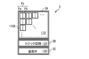
- Publication number
- WO2020209028A1 WO2020209028A1 PCT/JP2020/012220 JP2020012220W WO2020209028A1 WO 2020209028 A1 WO2020209028 A1 WO 2020209028A1 JP 2020012220 W JP2020012220 W JP 2020012220W WO 2020209028 A1 WO2020209028 A1 WO 2020209028A1
- Authority
- WO
- WIPO (PCT)
- Prior art keywords
- light receiving
- output
- unit
- region
- pixel
- Prior art date
- Legal status (The legal status is an assumption and is not a legal conclusion. Google has not performed a legal analysis and makes no representation as to the accuracy of the status listed.)
- Ceased
Links
Images
























Classifications
-
- H—ELECTRICITY
- H04—ELECTRIC COMMUNICATION TECHNIQUE
- H04N—PICTORIAL COMMUNICATION, e.g. TELEVISION
- H04N23/00—Cameras or camera modules comprising electronic image sensors; Control thereof
- H04N23/50—Constructional details
- H04N23/52—Elements optimising image sensor operation, e.g. for electromagnetic interference [EMI] protection or temperature control by heat transfer or cooling elements
-
- G—PHYSICS
- G01—MEASURING; TESTING
- G01S—RADIO DIRECTION-FINDING; RADIO NAVIGATION; DETERMINING DISTANCE OR VELOCITY BY USE OF RADIO WAVES; LOCATING OR PRESENCE-DETECTING BY USE OF THE REFLECTION OR RERADIATION OF RADIO WAVES; ANALOGOUS ARRANGEMENTS USING OTHER WAVES
- G01S7/00—Details of systems according to groups G01S13/00, G01S15/00, G01S17/00
- G01S7/48—Details of systems according to groups G01S13/00, G01S15/00, G01S17/00 of systems according to group G01S17/00
- G01S7/483—Details of pulse systems
- G01S7/486—Receivers
- G01S7/4861—Circuits for detection, sampling, integration or read-out
- G01S7/4863—Detector arrays, e.g. charge-transfer gates
-
- G—PHYSICS
- G01—MEASURING; TESTING
- G01C—MEASURING DISTANCES, LEVELS OR BEARINGS; SURVEYING; NAVIGATION; GYROSCOPIC INSTRUMENTS; PHOTOGRAMMETRY OR VIDEOGRAMMETRY
- G01C3/00—Measuring distances in line of sight; Optical rangefinders
- G01C3/02—Details
- G01C3/06—Use of electric means to obtain final indication
-
- G—PHYSICS
- G01—MEASURING; TESTING
- G01S—RADIO DIRECTION-FINDING; RADIO NAVIGATION; DETERMINING DISTANCE OR VELOCITY BY USE OF RADIO WAVES; LOCATING OR PRESENCE-DETECTING BY USE OF THE REFLECTION OR RERADIATION OF RADIO WAVES; ANALOGOUS ARRANGEMENTS USING OTHER WAVES
- G01S7/00—Details of systems according to groups G01S13/00, G01S15/00, G01S17/00
- G01S7/48—Details of systems according to groups G01S13/00, G01S15/00, G01S17/00 of systems according to group G01S17/00
- G01S7/481—Constructional features, e.g. arrangements of optical elements
- G01S7/4816—Constructional features, e.g. arrangements of optical elements of receivers alone
-
- G—PHYSICS
- G01—MEASURING; TESTING
- G01S—RADIO DIRECTION-FINDING; RADIO NAVIGATION; DETERMINING DISTANCE OR VELOCITY BY USE OF RADIO WAVES; LOCATING OR PRESENCE-DETECTING BY USE OF THE REFLECTION OR RERADIATION OF RADIO WAVES; ANALOGOUS ARRANGEMENTS USING OTHER WAVES
- G01S7/00—Details of systems according to groups G01S13/00, G01S15/00, G01S17/00
- G01S7/48—Details of systems according to groups G01S13/00, G01S15/00, G01S17/00 of systems according to group G01S17/00
- G01S7/497—Means for monitoring or calibrating
-
- H—ELECTRICITY
- H04—ELECTRIC COMMUNICATION TECHNIQUE
- H04N—PICTORIAL COMMUNICATION, e.g. TELEVISION
- H04N23/00—Cameras or camera modules comprising electronic image sensors; Control thereof
- H04N23/60—Control of cameras or camera modules
- H04N23/65—Control of camera operation in relation to power supply
-
- H—ELECTRICITY
- H04—ELECTRIC COMMUNICATION TECHNIQUE
- H04N—PICTORIAL COMMUNICATION, e.g. TELEVISION
- H04N25/00—Circuitry of solid-state image sensors [SSIS]; Control thereof
- H04N25/60—Noise processing, e.g. detecting, correcting, reducing or removing noise
- H04N25/63—Noise processing, e.g. detecting, correcting, reducing or removing noise applied to dark current
-
- H—ELECTRICITY
- H04—ELECTRIC COMMUNICATION TECHNIQUE
- H04N—PICTORIAL COMMUNICATION, e.g. TELEVISION
- H04N25/00—Circuitry of solid-state image sensors [SSIS]; Control thereof
- H04N25/70—SSIS architectures; Circuits associated therewith
-
- H—ELECTRICITY
- H04—ELECTRIC COMMUNICATION TECHNIQUE
- H04N—PICTORIAL COMMUNICATION, e.g. TELEVISION
- H04N25/00—Circuitry of solid-state image sensors [SSIS]; Control thereof
- H04N25/70—SSIS architectures; Circuits associated therewith
- H04N25/76—Addressed sensors, e.g. MOS or CMOS sensors
-
- H—ELECTRICITY
- H04—ELECTRIC COMMUNICATION TECHNIQUE
- H04N—PICTORIAL COMMUNICATION, e.g. TELEVISION
- H04N25/00—Circuitry of solid-state image sensors [SSIS]; Control thereof
- H04N25/70—SSIS architectures; Circuits associated therewith
- H04N25/76—Addressed sensors, e.g. MOS or CMOS sensors
- H04N25/77—Pixel circuitry, e.g. memories, A/D converters, pixel amplifiers, shared circuits or shared components
-
- H—ELECTRICITY
- H04—ELECTRIC COMMUNICATION TECHNIQUE
- H04N—PICTORIAL COMMUNICATION, e.g. TELEVISION
- H04N25/00—Circuitry of solid-state image sensors [SSIS]; Control thereof
- H04N25/70—SSIS architectures; Circuits associated therewith
- H04N25/76—Addressed sensors, e.g. MOS or CMOS sensors
- H04N25/77—Pixel circuitry, e.g. memories, A/D converters, pixel amplifiers, shared circuits or shared components
- H04N25/772—Pixel circuitry, e.g. memories, A/D converters, pixel amplifiers, shared circuits or shared components comprising A/D, V/T, V/F, I/T or I/F converters
- H04N25/773—Pixel circuitry, e.g. memories, A/D converters, pixel amplifiers, shared circuits or shared components comprising A/D, V/T, V/F, I/T or I/F converters comprising photon counting circuits, e.g. single photon detection [SPD] or single photon avalanche diodes [SPAD]
-
- H—ELECTRICITY
- H04—ELECTRIC COMMUNICATION TECHNIQUE
- H04N—PICTORIAL COMMUNICATION, e.g. TELEVISION
- H04N25/00—Circuitry of solid-state image sensors [SSIS]; Control thereof
- H04N25/70—SSIS architectures; Circuits associated therewith
- H04N25/76—Addressed sensors, e.g. MOS or CMOS sensors
- H04N25/78—Readout circuits for addressed sensors, e.g. output amplifiers or A/D converters
-
- H—ELECTRICITY
- H10—SEMICONDUCTOR DEVICES; ELECTRIC SOLID-STATE DEVICES NOT OTHERWISE PROVIDED FOR
- H10F—INORGANIC SEMICONDUCTOR DEVICES SENSITIVE TO INFRARED RADIATION, LIGHT, ELECTROMAGNETIC RADIATION OF SHORTER WAVELENGTH OR CORPUSCULAR RADIATION
- H10F30/00—Individual radiation-sensitive semiconductor devices in which radiation controls the flow of current through the devices, e.g. photodetectors
- H10F30/20—Individual radiation-sensitive semiconductor devices in which radiation controls the flow of current through the devices, e.g. photodetectors the devices having potential barriers, e.g. phototransistors
-
- H—ELECTRICITY
- H10—SEMICONDUCTOR DEVICES; ELECTRIC SOLID-STATE DEVICES NOT OTHERWISE PROVIDED FOR
- H10F—INORGANIC SEMICONDUCTOR DEVICES SENSITIVE TO INFRARED RADIATION, LIGHT, ELECTROMAGNETIC RADIATION OF SHORTER WAVELENGTH OR CORPUSCULAR RADIATION
- H10F30/00—Individual radiation-sensitive semiconductor devices in which radiation controls the flow of current through the devices, e.g. photodetectors
- H10F30/20—Individual radiation-sensitive semiconductor devices in which radiation controls the flow of current through the devices, e.g. photodetectors the devices having potential barriers, e.g. phototransistors
- H10F30/21—Individual radiation-sensitive semiconductor devices in which radiation controls the flow of current through the devices, e.g. photodetectors the devices having potential barriers, e.g. phototransistors the devices being sensitive to infrared, visible or ultraviolet radiation
- H10F30/22—Individual radiation-sensitive semiconductor devices in which radiation controls the flow of current through the devices, e.g. photodetectors the devices having potential barriers, e.g. phototransistors the devices being sensitive to infrared, visible or ultraviolet radiation the devices having only one potential barrier, e.g. photodiodes
- H10F30/225—Individual radiation-sensitive semiconductor devices in which radiation controls the flow of current through the devices, e.g. photodetectors the devices having potential barriers, e.g. phototransistors the devices being sensitive to infrared, visible or ultraviolet radiation the devices having only one potential barrier, e.g. photodiodes the potential barrier working in avalanche mode, e.g. avalanche photodiodes
-
- H—ELECTRICITY
- H10—SEMICONDUCTOR DEVICES; ELECTRIC SOLID-STATE DEVICES NOT OTHERWISE PROVIDED FOR
- H10F—INORGANIC SEMICONDUCTOR DEVICES SENSITIVE TO INFRARED RADIATION, LIGHT, ELECTROMAGNETIC RADIATION OF SHORTER WAVELENGTH OR CORPUSCULAR RADIATION
- H10F39/00—Integrated devices, or assemblies of multiple devices, comprising at least one element covered by group H10F30/00, e.g. radiation detectors comprising photodiode arrays
- H10F39/10—Integrated devices
- H10F39/12—Image sensors
Definitions
- the present disclosure relates to a light receiving device, for example, a light receiving device suitable for application to an avalanche photodiode.
- the present disclosure also relates to an imaging device and a distance measuring device including a light receiving device.
- An avalanche photodiode has a Geiger mode that operates with a bias voltage higher than the breakdown voltage and a linear mode that operates with a slightly higher bias voltage near the breakdown voltage.
- Geiger mode avalanche photodiodes are also called single photon avalanche photodiodes (SPADs).
- SPAD is a device that can detect one photon for each pixel by doubling the carriers generated by photoelectric conversion in the PN junction region of high electric field provided for each pixel.
- Patent Document 1 discloses a SPAD capable of reducing crosstalk to adjacent pixels due to light emission in a high electric field region and suppressing deterioration of the dark count rate due to the generation of dark current.
- the detection efficiency (Photon Detection. Efficiency: PDE) can be guaranteed only in a specific temperature range. It is desirable to provide a light receiving device capable of expanding the guaranteed range of the PDE, and an image pickup device and a distance measuring device provided with such a light receiving device.
- the light receiving device includes a pixel array in which light receiving elements including a high electric field region and a photoelectric conversion region are provided for each pixel.
- the plurality of light receiving elements provided for each pixel include a plurality of types of elements in which the temperature regions of high detection efficiency (Photon Detection. Efficiency: PDE) are different from each other and a part of the temperature regions overlap each other.
- PDE Photon Detection. Efficiency
- the image pickup apparatus includes the pixel array and a signal processing unit that generates a captured image based on a signal output from the pixel array.
- the distance measuring device includes the pixel array and a signal processing unit that measures the distance to the subject based on the signal output from the pixel array.
- the plurality of light receiving elements provided for each pixel have a plurality of PDE temperature regions that are different from each other and a part of the temperature regions that overlap each other. Includes different types of elements.
- the light receiving element whose high detection efficiency temperature region is relatively distributed on the low temperature side is used among the plurality of types of light receiving elements, and the charge is read out at a high temperature.
- FIG. 1 It is a figure which shows the schematic configuration example of the light receiving device which concerns on 1st Embodiment of this disclosure. It is a figure which shows the example which made up the light receiving device of FIG. 1 by a plurality of chips. It is a figure which shows the example which made up the light receiving device of FIG. 1 by a plurality of chips. It is a figure which shows the example which made up the light receiving device of FIG. 1 by one chip. It is a figure which shows the schematic structure example of the logic circuit of FIG. (A) is a figure showing a circuit configuration example of each pixel of the low temperature light receiving part of FIG. (B) is a figure showing a circuit configuration example of each pixel of the high temperature light receiving part of FIG.
- FIG. 6 (A) and 6 (B) are diagrams showing an example of the temperature dependence of PDE in APD. It is a figure which shows an example of the switching procedure of each light receiving part in the light receiving device of FIG.
- 6 (A) and 6 (B) are diagrams showing an example of the temperature dependence of PDE in APD. It is a figure which shows an example of the switching procedure of each light receiving part in the light receiving device of FIG. It is a figure which shows one modification of the schematic structure of the light receiving device of FIG. It is a figure which shows an example of the temperature dependence of PDE in APD of the light receiving device of FIG. It is a figure which shows an example of the switching procedure of each light receiving part in the light receiving device of FIG. It is a figure which shows the schematic configuration example of the light receiving device which concerns on 2nd Embodiment of this disclosure. It is a figure which shows the example which made up the light receiving device of FIG. 19 by a plurality of chips.
- FIG. 19 It is a figure which shows the example which made up the light receiving device of FIG. 19 by a plurality of chips. It is a figure which shows the example which made up the light receiving device of FIG. 19 by one chip. It is a figure which shows the schematic structure example of the logic circuit of FIG. (A) is a figure which shows the circuit structure example of the low temperature pixel of FIG. (B) It is a figure which shows the circuit structure example of the high temperature pixel of FIG. It is a figure which shows the cross-sectional composition example of the low temperature pixel of FIG. It is a figure which shows the cross-sectional composition example of the high temperature pixel of FIG. It is a figure which shows the example of the upper surface structure of the light receiving part of FIG.
- FIG. 3 is a diagram showing an example in which the light receiving device of FIG. 32 is composed of a plurality of chips.
- FIG. 3 is a diagram showing an example in which the light receiving device of FIG.
- FIG. 32 is composed of a plurality of chips. It is a figure which shows the example which made up the light receiving device of FIG. 32 with one chip. It is a figure which shows the schematic structure example of the logic circuit of FIG. (A) is a figure which shows the circuit configuration example of the low temperature sub-pixel of FIG. 32. (B) is a diagram showing a circuit configuration example of the high temperature sub-pixel of FIG. 32. It is a figure which shows the cross-sectional composition example of each pixel of FIG. It is a figure which shows the example of the upper surface structure of the light receiving part of FIG. 32. It is a figure which shows an example of the temperature dependence of PDE in APD of the light receiving device of FIG.
- FIG. 32 It is a figure which shows one modification of the schematic structure of the light receiving device of FIG. 32. It is a figure which shows an example of the switching method of a light receiving part, an output signal or a sub pixel. It is a figure which shows one modification of the schematic structure of the light receiving device of FIG. 44. It is a figure which shows one modification of the schematic structure of the light receiving device of FIG. 45. It is a figure which shows one modification of the schematic structure of the light receiving device of FIG. It is a figure which shows the application example to the image pickup apparatus of the light receiving device which concerns on each said embodiment and the modification. It is a figure which shows the application example to the distance measuring apparatus of the light receiving device which concerns on each said embodiment and the modification. It is a block diagram which shows an example of the schematic structure of a vehicle control system. It is explanatory drawing which shows an example of the installation position of the vehicle exterior information detection unit and the image pickup unit.
- APD avalanche photodiode
- the technology described below can be applied to light receiving devices. Further, since it can be particularly applied to an avalanche photodiode (APD) as a light receiving device, APD will be described here as an example.
- the APD has a Geiger mode that operates with a bias voltage higher than the breakdown voltage and a linear mode that operates with a slightly higher bias voltage near the breakdown voltage. Geiger mode avalanche photodiodes are also called single photon avalanche photodiodes (SPADs).
- SPAD is a device capable of detecting one photon for each pixel by multiplying the carrier generated by photoelectric conversion in a PN junction region of a high electric field provided for each pixel.
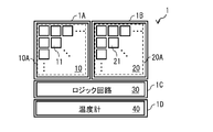
- FIG. 1 shows a schematic configuration example of the light receiving device 1.
- the light receiving device 1 includes, for example, two light receiving units (a low temperature light receiving unit 10 and a high temperature light receiving unit 20), a logic circuit 30, and a thermometer 40.
- the low temperature light receiving unit 10 has a pixel array 10A.
- the pixel array 10A includes a plurality of pixels 11.
- the high temperature light receiving unit 20 has a pixel array 20A.
- the pixel array 10A includes a plurality of pixels 21.
- the pixel arrays 10A and 20A correspond to a specific example of the "pixel array" of the present disclosure.
- the pixel array 10A and the pixel array 20A are arranged next to each other.
- the logic circuit 30 outputs the output signal Dout obtained based on the output signals from the two light receiving units (low temperature light receiving unit 10 and high temperature light receiving unit 20) to the outside. Pixels 11 and 21 will be described in detail later.
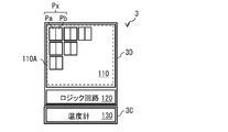
- the two light receiving parts are formed on separate chips (chip 1A, chip 1B), for example, as shown in FIG.
- a low temperature light receiving portion 10 is formed on the chip 1A
- a high temperature light receiving portion 20 is formed on the chip 1B.
- the chips 1A and 1B include, for example, a silicon substrate.
- the low temperature light receiving unit 10 is formed on the silicon substrate (first semiconductor substrate) of the chip 1A
- the high temperature light receiving unit 20 is the silicon substrate of the chip 1B, that is, the silicon substrate included in the low temperature light receiving unit 10. Is formed on a separate silicon substrate (second semiconductor substrate).
- the logic circuit 30 is formed on a chip 1C separate from the chips 1A and 1B, for example, and the thermometer 40 is formed on a chip 1C separate from the chips 1A, 1B and 1C, for example. It is formed in 1D.
- the chips 1A and 1B may be bonded on the chip 1C, or the chips 1A, 1B, 1C and 1D may be bonded on a common support substrate.
- the chip 1D may be attached to the back surface of the chip 1C.
- two light receiving units (low temperature light receiving unit 10 and high temperature light receiving unit 20) may be formed on a common chip 1E, for example, as shown in FIG.
- the chip 1E is configured to include, for example, a silicon substrate, and two light receiving portions (low temperature light receiving portion 10 and high temperature light receiving portion 20) are formed on a common silicon substrate.
- the logic circuit 30 may be formed on the same chip 1E as the two light receiving units (low temperature light receiving unit 10 and high temperature light receiving unit 20), for example, as shown in FIG. ..
- the two light receiving parts (low temperature light receiving part 10 and high temperature light receiving part 20) and the logic circuit 30 are formed on a common silicon substrate.
- two light receiving units (low temperature light receiving unit 10, high temperature light receiving unit 20), a logic circuit 30, and a thermometer 40 are formed on a common chip 1F, for example, as shown in FIG. It may have been.
- the chip 1F is configured to include, for example, a silicon substrate, and the two light receiving units (low temperature light receiving unit 10, high temperature light receiving unit 20), the logic circuit 30, and the thermometer 40 share a common silicon substrate. Is formed in.
- the thermometer 40 measures the temperature of the two light receiving units (low temperature light receiving unit 10 and high temperature light receiving unit 20), and outputs the measurement result to the logic circuit 30.
- the thermometer 40 is composed of, for example, a silicon diode temperature sensor.
- the thermometer 40 may be composed of, for example, a silicon diode temperature sensor, or may be composed of another temperature sensor.
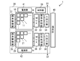
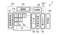
- FIG. 5 shows a schematic configuration example of the logic circuit 30.
- FIG. 6A shows an example of a circuit configuration of each pixel 11.
- FIG. 6B shows an example of a circuit configuration of each pixel 21.
- the logic circuit 30 includes, for example, a pixel drive unit 31, a MUX (multiplexer) 32, a signal processing unit 33, and an input / output unit 34.
- the pixel drive unit 31 drives each pixel 11 in the low temperature light receiving unit 10.
- the MUX 32, the signal processing unit 33, and the input / output unit 34 process the output from the low temperature light receiving unit 10.
- the output of the input / output unit 34 is referred to as an output signal D1.
- the logic circuit 30 further includes, for example, a pixel drive unit 35, a MUX (multiplexer) 36, a signal processing unit 37, an input / output unit 38, a control unit 39, and power supply units 41 and 42.
- the pixel drive unit 35 drives each pixel 21 in the high temperature light receiving unit 20.
- the MUX 36, the signal processing unit 37, and the input / output unit 38 process the output from the high temperature light receiving unit 20.
- the output of the input / output unit 38 is referred to as an output signal D2.
- the power supply unit 41 supplies a predetermined voltage (for example, power supply voltages Va, Ve) to each pixel 11.
- the power supply unit 42 supplies a predetermined voltage (for example, power supply voltages Vb, Ve) to each pixel 21.
- the low temperature light receiving unit 10 has a plurality of pixels 11 arranged two-dimensionally.
- Each pixel 11 includes, for example, an APD (avalanche photodiode) 12 and a transistor Tr1 electrically connected to the node of the APD 12.
- the APD 12 corresponds to a specific example of the "first light receiving element" of the present disclosure.
- the transistor Tr1 is turned on according to the control signal input to the gate, so that the detection signal generated by the APD 12 is output to the signal line DTL (described later).
- the transistor Tr1 is composed of, for example, a field effect transistor thin film transistor (TFT).
- TFT field effect transistor thin film transistor
- the high temperature light receiving unit 20 has a plurality of pixels 21 arranged two-dimensionally.
- Each pixel 21 includes, for example, an APD (avalanche photodiode) 22 and a transistor Tr2 electrically connected to the node of the APD 22.
- the APD22 corresponds to a specific example of the "second light receiving element" of the present disclosure.
- the transistor Tr2 is turned on according to the control signal input to the gate, so that the detection signal generated by the APD 22 is output to the signal line DTL.
- the transistor Tr2 is composed of, for example, a field effect transistor thin film transistor (TFT).
- TFT field effect transistor thin film transistor
- APDs 12 and 22 are photodiodes (single photon avalanche photodiodes) that amplify the electric charge generated when incident light is incident and output the detection signal obtained thereby.
- the power supply voltage Va supplied to the anode of the APD 12 is, for example, a negative bias (negative potential) of about ⁇ 20 V.
- the power supply voltage Vb supplied to the anode of the APD 22 is, for example, a negative bias (negative potential) of about ⁇ 20 V.
- the power supply voltage Va and the power supply voltage Vb may be equal to each other or different from each other.
- the power supply voltage Ve is supplied to the cathodes of the APDs 12 and 22 via the source and drain of the transistors Tr1 and Tr2.
- the power supply voltage Ve is, for example, a positive potential of about 3 V.
- the transistors Tr1 and Tr2 are constant current sources that operate in the saturation region, and perform passive quenching by acting as a quenching resistor.
- the low temperature light receiving unit 10 and the high temperature light receiving unit 20 each further have a plurality of signal line DTLs and a plurality of gate line GTLs.
- the low temperature light receiving unit 10 and the high temperature light receiving unit 20 further have a plurality of power supply lines PWL1 and PWL2 and a ground line GND, respectively.
- the low temperature light receiving unit 10 further includes a switch element SW1, inverters INV1 and INV2, and a latch circuit 18.
- the high temperature light receiving unit 20 further includes a switch element SW2, inverters INV3 and 4, and a latch circuit 28.
- the signal line DTL is a wiring for reading the detection signal from the APDs 12 and 22.
- the gate line GTL is a wiring for inputting a control signal for on / off control of the transistors Tr1 and Tr2 to the gate of the transistors Tr1 and Tr2.
- the power line PWL1 is a wiring for determining the anode potentials of the APDs 12 and 22.
- the power line PWL2 is a wiring for determining the cathode potential of the APDs 12 and 22.
- the gates of the transistors Tr1 and Tr2 are connected to the gate line GTL.
- the source or drain of the transistors Tr1 and Tr2 is connected to the cathode of the APD12 and 22 and the input terminals of the inverters INV1 and INV3.
- the output terminals of the inverters INV1 and INV3 are connected to the signal line DTL. Of the sources and drains of the transistors Tr1 and Tr2, the electrodes that are not connected to the cathode are connected to the power supply line PWL2.
- the cathodes of the APDs 12 and 22 are connected to the source or drain of the transistors Tr1 and Tr2, and the anodes of the APDs 12 and 22 are connected to the power supply line PWL1.
- the input terminals of the inverters INV2 and INV4 are connected to the latch circuits 18 and 28, and the output terminals of the inverters INV2 and INV4 are connected to the on / off control terminals of the switch elements SW1 and SW2.
- the switch element SW1 is connected to the APD 12 in parallel.
- the switch element SW2 is connected to the APD 22 in parallel.
- the switch elements SW1 and SW2 turn on and off, for example, the gating control signal which is the output of the latch circuits 18 and 28 according to the gating inverting signal inverted by the inverters INV2 and INV4.
- the latch circuits 18 and 28 are gating controls that control the pixels 11 and 21 to either active pixels or inactive pixels based on the trigger signal SET supplied from the pixel drive units 31 and 35 and the address data DEC.
- the signal is supplied to the inverters INV2 and INV4.
- the inverters INV2 and INV4 generate a gating inversion signal in which the gating control signal is inverted and supply it to the switch elements SW1 and SW2.
- the trigger signal SET is a timing signal indicating the timing for switching the gating control signal
- the address data DEC is set as the active pixel among a plurality of pixels 11 and 21 arranged in a matrix in the pixel arrays 10A and 20A. It is data which shows the address of the pixel to perform.
- the trigger signal SET and the address data DEC are supplied from the pixel drive units 31 and 35.
- the latch circuits 18 and 28 read the address data DEC at a predetermined timing indicated by the trigger signal SET. Then, when the pixel addresses indicated by the address data DEC include their own (pixels 11 and 21) pixel addresses, the latch circuits 18 and 28 set their own pixels 11 and 21 as active pixels. The gating control signal of Hi (1) is output. On the other hand, when the pixel address indicated by the address data DEC does not include the pixel address of its own (pixels 11 and 21), Lo (0) for setting its own pixels 11 and 21 as inactive pixels. Outputs a gating control signal.
- the Lo (0) gating inversion signal inverted by the inverters INV2 and INV4 is supplied to the switch elements SW1 and SW2.
- the gating inversion signal of Hi (1) is supplied to the switch elements SW1 and SW2. Therefore, the switch elements SW1 and SW2 are turned off (disconnected) when the pixels 11 and 21 are set as active pixels, and turned on (connected) when the pixels 11 and 21 are set as inactive pixels.
- the inverters INV2 and INV4 output a Hi detection signal when the cathode voltage as an input signal is Lo, and output a Lo detection signal when the cathode voltage is Hi.
- the inverters INV2 and INV4 are output units that output the incident of photons on the APDs 12 and 22 as a detection signal.
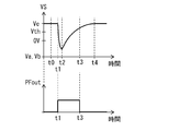
- FIG. 7 is a graph showing changes in the cathode voltage VS and the detection signal PFout of the APDs 12 and 22 in response to the incident of photons.
- the power supply voltage Ve is supplied to the cathodes of the APDs 12 and 22 and the power supply voltages Va and Vb are supplied to the anodes, a reverse voltage larger than the yield voltage VBD is applied to the APDs 12 and 22 to cause the APDs 12 and 22. Is set to Geiger mode. In this state, the cathode voltage VS of the APDs 12 and 22 is the same as the power supply voltage Ve, for example, at time t0 in FIG.
- APDs 12 and 22 When a photon is incident on APDs 12 and 22 set in Geiger mode, avalanche multiplication occurs and a current flows through APDs 12 and 22.
- the cathode voltage VS of APD12, 22 becomes lower than 0V
- the anode-cathode voltage of APD12, 22 becomes lower than the yield voltage VBD, so that the avalanche amplification is stopped.
- the current generated by the avalanche amplification flows through the transistors Tr1 and Tr2 to generate a voltage drop, and the cathode voltage VS becomes lower than the breakdown voltage VBD as the generated voltage drop causes the avalanche amplification.
- the operation of stopping is the quenching operation.
- the inverters INV2 and INV4 output the Lo detection signal PFout when the cathode voltage VS, which is the input voltage, is equal to or higher than the predetermined threshold voltage Vth, and the Hi detection signal PFout when the cathode voltage VS is less than the predetermined threshold voltage Vth. Is output. Therefore, when a photon is incident on the APDs 12 and 22, an avalanche multiplication occurs, the cathode voltage VS decreases, and the threshold voltage Vth is lowered, the detection signal PFout is inverted from a low level to a high level.
- the cathode voltage VS rises, and becomes the threshold voltage Vth or more, the detection signal PFout is inverted from the high level to the low level.
- the gating inversion signal of Hi (1) is supplied to the switch elements SW1 and SW2, and the switch elements SW1 and SW2 are turned on.
- the switch elements SW1 and SW2 are turned on, the cathode voltage VS of the APDs 12 and 22 becomes 0V.
- the voltage between the anode and the cathode of the APDs 12 and 22 becomes equal to or lower than the yield voltage VBD, so that even if photons enter the APDs 12 and 22, they do not react.
- the pixel drive unit 31 is composed of, for example, a shift register, an address decoder, or the like, and drives each pixel 11 in units of lines, for example.
- the detection signal output from each pixel 11 of the pixel row selectively scanned by the pixel drive unit 31 is supplied to the MUX 32 via each signal line DTL.
- the pixel drive unit 35 is composed of, for example, a shift register, an address decoder, or the like, and drives each pixel 21 in units of rows, for example.
- the detection signal output from each pixel 21 of the pixel row selectively scanned by the pixel drive unit 35 is supplied to the MUX 36 via each signal line DTL.
- MUX 32, 36 selects the output from the active pixel according to the switching between the active pixel and the inactive pixel in the pixel arrays 10A and 20A. Then, the MUX 32 and 36 output the pixel signal input from the selected active pixel to the signal processing units 33 and 37.
- the signal processing units 33 and 37 are, for example, time measuring units.
- the time measuring unit receives light after the light source emits light based on the pixel signals of the active pixels supplied from the MUXs 32 and 36 and the emission timing signal indicating the emission timing of the light source (described later). Generate a count value corresponding to the time until it is done.
- the time measurement unit is also called a TDC (Time to Digital Converter).
- the light emission timing signal is supplied from the outside via the input / output units 34 and 38.
- the signal processing units 33 and 37 may be counter units.
- the counter unit counts, for example, the number of detection signals input from the MUXs 32 and 36 for a predetermined period, and outputs the count value for each pixel obtained thereby.
- the power supply unit 41 is connected to each power supply line PWL1 connected to each pixel 11, and a negative bias voltage (power supply voltage Va) is applied to each power supply line PWL to which each pixel 11 is connected.
- the power supply unit 41 is further connected to each power supply line PWL2 connected to each pixel 11, and applies a predetermined voltage (power supply voltage Ve) to each power supply line PWL2 to which each pixel 11 is connected.
- the power supply unit 42 is connected to each power supply line PWL1 connected to each pixel 21, and applies a negative bias voltage (power supply voltage Vb) to each power supply line PWL1 connected to each pixel 21.
- the power supply unit 42 is further connected to each power supply line PWL2 connected to each pixel 21, and applies a predetermined voltage (power supply voltage Ve) to each power supply line PWL2 connected to each pixel 21.
- the power supply voltage Va preferably has a value that maximizes the PDE of the APD12.
- the power supply voltage Vb preferably has a value that maximizes the PDE of the APD22.
- the input / output unit 34 selects whether or not to output the output signal D1 output from the signal processing unit 33 as the output signal Dout according to the control from the control unit 39.
- the input / output unit 38 selects whether or not to output the output signal D2 output from the signal processing unit 37 as the output signal Dout according to the control from the control unit 39.
- the input / output unit 34 selects whether or not to output the output signal D1 output from the signal processing unit 33 as the output signal Dout according to the temperature of the thermometer 40.
- the input / output unit 38 selects whether or not to output the output signal D2 output from the signal processing unit 37 as the output signal Dout according to the temperature of the thermometer 40.
- the control unit 39 receives a clock or the like given from the outside, and also outputs data such as internal information of the light receiving device 1.
- the control unit 39 further has a timing generator that generates various timing signals, and based on the various timing signals generated by the timing generator, the pixel drive units 31, 35, MUX 32, 36, and the signal processing unit 33 , 37, input / output units 34, 38, power supply units 41, 42, and the like.
- the control unit 39 controls the output from the logic circuit 30. In the present embodiment, the control unit 39 outputs either the output signal D1 or the output signal D2 from the logic circuit 30 as the output signal Dout.
- the control unit 39 includes the pixel drive unit 31, MUX 32, the signal processing unit 33 and the input / output unit 34, and the pixel drive unit 35, MUX 36, the signal processing unit 37 and the input / output unit 38 according to the temperature of the thermometer 40.
- the logic circuit 30 may be controlled so as to drive only one of them.
- the control unit 39 may control the power supply units 41 and 42 so as to apply a negative bias voltage to only one of each APD 12 and each APD 22 according to the temperature of the thermometer 40.
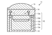
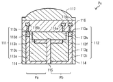
- FIG. 8 shows a cross-sectional configuration example of each pixel 11 of the low temperature light receiving unit 10.
- the low temperature light receiving unit 10 has, for example, an n-type semiconductor region 12a and a p-type semiconductor region 12b.
- the p-type semiconductor region 12b is formed in contact with the lower portion of the n-type semiconductor region 12a.
- the n-type semiconductor region 12a and the p-type semiconductor region 12b are formed in the well layer 12c.
- the well layer 12c may be an n-type semiconductor layer or a p-type semiconductor layer.
- the well layer 12c is preferably an n-type semiconductor layer or a p-type semiconductor layer having a low impurity concentration of 1 ⁇ 10 14 cm -3 or less, for example. In this case, the well layer 12c is likely to be depleted, and the PDE of APD12 can be improved.
- the n-type semiconductor region 12a is, for example, Si (silicon) and is an n-type semiconductor region having a high impurity concentration.
- the p-type semiconductor region 12b is, for example, Si (silicon) and is a p-type semiconductor region having a high impurity concentration.
- the p-type semiconductor region 12b constitutes a pn junction at the interface with the n-type semiconductor region 12a.
- the region including the pn junction is the high electric field region, and the n-type semiconductor region 12a is the photoelectric conversion region.
- the p-type semiconductor region 12b has a multiplication region that avalanche-amplifies the carriers generated by the incident light to be detected.
- the p-type semiconductor region 12b is preferably depleted.
- the PDE of the APD 12 can be improved.
- the n-type semiconductor region 12a functions as a cathode and is connected to a circuit via a contact 16.
- the anode 12d with respect to the cathode is in the same layer as the n-type semiconductor region 12a, and is formed between the n-type semiconductor region 12a and the separation region 13.
- the anode 12d is connected to the circuit via the contact 17.
- a separation region 13 for separating the APD 12s is formed, and a hole accumulation region 12e is formed between the separation region 13 and the well layer 12c.
- the hole storage region 12e is formed below the anode 12d and is formed in a state of being electrically connected to the anode 12d. Further, the hole accumulation region 12e is formed between the well layer 12c and the separation region 13. Further, the hole accumulation region 12e is also formed in contact with the lower part of the well layer 12c.
- the hole accumulation region 12e is formed in a portion where different materials are in contact with each other.
- the separation region 13 is made of, for example, a silicon oxide film, and is made of a material different from that of the well layer 12c. In this case, the hole accumulation region 12e is formed in order to suppress the dark current generated at the interface.
- the hole storage region 12e can be formed as, for example, a p-type semiconductor region.
- the separation region 13 is formed between two APD 12s adjacent to each other and separates each APD 12. That is, the separation region 13 is formed so that a multiplication region is formed in a one-to-one correspondence with each APD 12.
- the separation region 13 is formed in a two-dimensional grid pattern so as to completely surround each APD 12.
- the separation region 13 is formed so as to penetrate from the upper surface side to the lower surface side of the well layer 12c in the stacking direction.
- the separation region 13 may have a configuration in which only a part of the separation region 13 penetrates and is inserted halfway through the substrate, other than the configuration in which the separation region 13 completely penetrates from the upper surface side to the lower surface side.
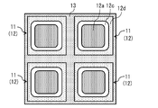
- FIG. 9 shows a plan configuration example of the low temperature light receiving unit 10.
- FIG. 9 shows an example in which four 2 ⁇ 2 APD12s are arranged. As described above, each APD 12 is separated from each other by a separation region 13 formed in a grid pattern. An anode 12d is formed inside the separation region 13. An n-type semiconductor region 12a is formed in the central portion of the APD 12, and a well layer 12c is formed between the anode 12d and the n-type semiconductor region 12a.
- the n-type semiconductor region 12a has, for example, a quadrangular shape.
- the planar shape of the n-type semiconductor region 12a is not limited to a quadrangular shape, and may be, for example, a circular shape.
- n-type semiconductor region 12a When the n-type semiconductor region 12a has a quadrangular shape, a wide area of the multiplication region can be secured, so that PDE can be improved. When the n-type semiconductor region 12a has a circular shape, electric field concentration in the APD 12 can be suppressed, and unintended breakdown can be reduced.
- FIG. 10 shows a cross-sectional configuration example of each pixel 21 of the high temperature light receiving unit 20.
- the high temperature light receiving unit 20 has, for example, an n-type semiconductor region 22a and a p-type semiconductor region 22b.
- the p-type semiconductor region 22b is formed in contact with the lower portion of the n-type semiconductor region 22a.
- the n-type semiconductor region 22a and the p-type semiconductor region 22b are formed in the well layer 22c.
- the well layer 22c may be an n-type semiconductor layer or a p-type semiconductor layer.
- the well layer 22c is preferably an n-type semiconductor layer or a p-type semiconductor layer having a low impurity concentration of 1 ⁇ 10 14 cm -3 or less, for example. In this case, the well layer 22c is easily depleted, and the PDE of the APD 22 can be improved.
- the n-type semiconductor region 22a is, for example, Si (silicon) and is an n-type semiconductor region having a high impurity concentration.
- the p-type semiconductor region 22b is, for example, Si (silicon) and is a p-type semiconductor region having a high impurity concentration.
- the p-type semiconductor region 22b constitutes a pn junction at the interface with the n-type semiconductor region 22a.
- the region including the pn junction is the high electric field region, and the n-type semiconductor region 22a is the photoelectric conversion region.
- the p-type semiconductor region 22b has a multiplication region that avalanche-amplifies the carriers generated by the incident light to be detected.
- the p-type semiconductor region 22b is preferably depleted.
- the PDE of the APD 22 can be improved.
- the n-type semiconductor region 22a functions as a cathode and is connected to a circuit via a contact 26.
- the anode 22d with respect to the cathode is in the same layer as the n-type semiconductor region 22a, and is formed between the n-type semiconductor region 22a and the separation region 23.
- the anode 22d is connected to the circuit via the contact 27.
- a separation region 23 for separating the APDs 22 from each other is formed, and a hole accumulation region 22e is formed between the separation region 23 and the well layer 22c.
- the hole storage region 22e is formed below the anode 22d and is formed in a state of being electrically connected to the anode 22d. Further, the hole accumulation region 22e is formed between the well layer 22c and the separation region 23. Further, the hole accumulation region 22e is also formed in contact with the lower part of the well layer 22c.
- the hole accumulation region 22e is formed in a portion where different materials are in contact with each other.
- the separation region 23 is made of, for example, a silicon oxide film, and is made of a material different from that of the well layer 22c. In this case, the hole accumulation region 22e is formed in order to suppress the dark current generated at the interface.
- the hole storage region 22e can be formed as, for example, a p-type semiconductor region.
- the separation region 23 is formed between two APD 22s adjacent to each other and separates each APD 22. That is, the separation region 23 is formed so that a multiplication region is formed in a one-to-one correspondence with each APD 22.
- the separation region 23 is formed in a two-dimensional grid pattern so as to completely surround each APD 22.
- the separation region 23 is formed so as to penetrate from the upper surface side to the lower surface side of the well layer 22c in the stacking direction.
- the separation region 23 may have a configuration in which only a part of the separation region 23 penetrates and is inserted halfway through the substrate, other than the configuration in which the separation region 23 penetrates completely from the upper surface side to the lower surface side.
- FIG. 11 shows an example of a plan configuration of the high temperature light receiving unit 20.
- FIG. 11 shows an example in which four 2 ⁇ 2 APD22s are arranged.
- each APD 22 is separated from each other by a separation region 23 formed in a grid pattern.
- An anode 22d is formed inside the separation region 23.
- An n-type semiconductor region 22a is formed in the central portion of the APD 22, and a well layer 22c is formed between the anode 22d and the n-type semiconductor region 22a.
- the n-type semiconductor region 22a has, for example, a quadrangular shape.
- the planar shape of the n-type semiconductor region 22a is not limited to a quadrangular shape, and may be, for example, a circular shape.
- n-type semiconductor region 22a When the n-type semiconductor region 22a has a quadrangular shape, a wide area of the multiplication region can be secured, so that PDE can be improved. When the n-type semiconductor region 22a has a circular shape, electric field concentration in the APD 22 can be suppressed, and unintended breakdown can be reduced.
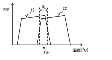
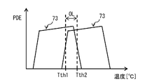
- FIG. 12 shows an example of the temperature dependence of the PDEs of APDs 12 and 22.
- APD12 has a high PDE in the low temperature range.
- APD22 has a high PDE in a high temperature region.
- the high PDE temperature region is relatively distributed on the low temperature side.
- the high PDE temperature region is relatively distributed on the high temperature side.
- the high PDE temperature region of APD12 and the high PDE temperature region of APD22 are different from each other, and a part of the high PDE temperature region of APD12 and a part of the high PDE temperature region of APD22 are They overlap each other.
- the “high PDE temperature region” refers to a temperature region larger than half the peak value in the PDE temperature distribution. As shown in FIG. 12, in the overlapping region OL of the high PDE in the APDs 12 and 22, the region on the high temperature side of the high PDE temperature region of the APD 12 and the region on the low temperature side of the high PDE temperature region of the APD 22 They overlap each other.
- At least one of the thickness of the type semiconductor regions 12d and 22d) and the area of the multiplication region (p-type semiconductor regions 12d and 22d) are different from each other.
- the high PDE temperature region of APD12 and the high PDE temperature region of APD22 are different from each other.
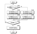
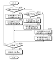
- FIG. 13 shows an example of the switching procedure of the low temperature light receiving unit 10 and the high temperature light receiving unit 20 (output signals D1 and D2).
- the control unit 39 determines whether or not the temperature of the thermometer 40 is equal to or higher than a predetermined temperature (threshold value Tth) in the overlapping region OL (step S101).
- a predetermined temperature threshold value Tth
- the control unit 39 receives light for low temperature by, for example, stopping the operations of the pixel drive unit 31, MUX 32, the signal processing unit 33, and the input / output unit 34.
- the operation of the unit 10 is stopped, and the high temperature light receiving unit 20 is driven by operating the pixel drive unit 35, the MUX 36, the signal processing unit 37, and the input / output unit 38 (step S102).
- the control unit 39 may control the power supply units 41 and 42 so as to apply a negative bias voltage only to each APD 22.
- the output signal D1 is not output from the low temperature light receiving unit 10
- the output signal D2 is output from the high temperature light receiving unit 20.
- the control unit 39 outputs the output signal D2 from the logic circuit 30 as the output signal Dout (step S103).
- step S101 when the temperature of the thermometer 40 is less than the threshold value Tth, the control unit 39 operates, for example, the pixel drive unit 31, the MUX 32, the signal processing unit 33, and the input / output unit 34 to reduce the temperature.
- the control unit 39 may control the power supply units 41 and 42 so as to apply a negative bias voltage only to each APD 12.
- the output signal D1 is output from the low temperature light receiving unit 10
- the output signal D2 is not output from the high temperature light receiving unit 20.
- the control unit 39 outputs the output signal D1 from the logic circuit 30 as the output signal Dout (step S105).
- the control unit 39 executes steps S101 to S105 above (step S106) unless instructed to end the measurement by the light receiving device 1.
- the control unit 39 stops the operation of the low temperature light receiving unit 10 and the high temperature light receiving unit 20 by, for example, stopping the operation of the logic circuit 30. Step S107).
- control unit 39 may execute the following switching procedure.
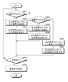
- FIG. 15 shows an example of the switching procedure of the low temperature light receiving unit 10 and the high temperature light receiving unit 20 (output signal D1 and output signal D2).
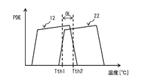
- the control unit 39 determines whether or not the temperature of the thermometer 40 is equal to or higher than the upper limit temperature (threshold value Tth2) of the overlapping region OL (step S201).
- the control unit 39 receives light for low temperature by, for example, stopping the operations of the pixel drive unit 31, MUX 32, the signal processing unit 33, and the input / output unit 34.
- the operation of the unit 10 is stopped, and the high temperature light receiving unit 20 is driven by operating the pixel drive unit 35, the MUX 36, the signal processing unit 37, and the input / output unit 38 (step S202).
- the control unit 39 may control the power supply units 41 and 42 so as to apply a negative bias voltage only to each APD 22.
- the output signal D1 is not output from the low temperature light receiving unit 10
- the output signal D2 is output from the high temperature light receiving unit 20.
- the control unit 39 outputs the output signal D2 from the logic circuit 30 as the output signal Dout (step S203).
- step S201 when the temperature of the thermometer 40 is less than the threshold value Tth2, the control unit 39 determines whether or not the temperature of the thermometer 40 is equal to or less than the lower limit temperature (threshold value Tth1) of the overlapping region OL. (Step S204).
- the control unit 39 operates, for example, the pixel drive unit 31, the MUX 32, the signal processing unit 33, and the input / output unit 34 to operate the low temperature light receiving unit 10.
- the operation of the high temperature light receiving unit 20 is stopped by stopping the operations of the pixel driving unit 35, the MUX 36, the signal processing unit 37, and the input / output unit 38 (step S205).
- control unit 39 may control the power supply units 41 and 42 so as to apply a negative bias voltage only to each APD 12.
- the output signal D1 is output from the low temperature light receiving unit 10, and the output signal D2 is not output from the high temperature light receiving unit 20.
- the control unit 39 outputs the output signal D1 from the logic circuit 30 as the output signal Dout (step S206).
- step S204 when the temperature of the thermometer 40 is higher than the threshold value Tth1, the control unit 39 operates, for example, the pixel drive unit 31, MUX 32, the signal processing unit 33, and the input / output unit 34 to receive low temperature light.
- the high temperature light receiving unit 20 is driven by operating the pixel drive unit 35, the MUX 36, the signal processing unit 37, and the input / output unit 38 (step S207).
- the control unit 39 controls the power supply units 41 and 42 so as to apply a negative bias voltage to the APDs 12 and 22.
- the output signal D1 is output from the low temperature light receiving unit 10
- the output signal D2 is output from the high temperature light receiving unit 20.
- the control unit 39 outputs a signal obtained by adding the output signal D1 and the output signal D2 from the logic circuit 30 as the output signal Dout (step S208).
- the control unit 39 executes steps S208 to S208 from step S201 above unless instructed to end the measurement by the light receiving device 1 (step S209).
- the control unit 39 stops the operation of the low temperature light receiving unit 10 and the high temperature light receiving unit 20 by, for example, stopping the operation of the logic circuit 30. Step S210).
- the control unit 39 controls the power supply units 41 and 42 so as not to apply a negative bias voltage to the APDs 12 and 22, for example.
- the control unit 39 always drives the low temperature light receiving unit 10 and the high temperature light receiving unit 20 regardless of the temperature of the thermometer 40, and adds the output signal D1 and the output signal D2 as the output signal Dout.
- the signal may be output from the logic circuit 30.
- the avalanche photodiode has a Geiger mode that operates with a bias voltage higher than the breakdown voltage and a linear mode that operates with a slightly higher bias voltage near the breakdown voltage.
- Geiger mode avalanche photodiodes are also called single photon avalanche photodiodes (SPADs).
- the SPAD is a device capable of detecting one photon for each pixel by doubling the carriers generated by photoelectric conversion in a PN junction region of a high electric field provided for each pixel.
- the plurality of light receiving elements provided for each of the pixels 11 and 21 include two types of light receiving elements (APD12, 22) in which the temperature regions of the PDEs are different from each other and a part of the temperature regions overlap each other. include.
- APD12, 22 the APD12 whose temperature region with high detection efficiency is relatively distributed on the low temperature side is used among the two types of light receiving elements, and when the charge is read out at a high temperature
- the APD22 in which the temperature region with high detection efficiency is relatively distributed on the high temperature side among the two types of light receiving elements, the decrease in PDE is suppressed at both low temperature and high temperature.
- the guaranteed range of PDE can be expanded as compared with the case where only one of APD12 and APD22 is used.
- the chip 1A and the chip 1B are manufactured in separate steps. be able to. As a result, the manufacturing process can be simplified and the yield can be improved as compared with the case where the plurality of APD12s and the plurality of APD22s are formed on a common chip.
- the plurality of APDs 12 and 22 are formed on a common semiconductor substrate, the plurality of APDs 12 are formed as compared with the case where the plurality of APDs 12 and the plurality of APDs 22 are formed on different semiconductor substrates.
- the gap between the formed pixel array 10A and the pixel array 20A on which a plurality of APDs 22 are formed can be narrowed.
- the optical axis of the pixel array 10A and the optical axis of the pixel array 20A can be brought close to each other, so that it becomes easy to design an optical system that guides the incident light to the pixel array 10A and the pixel array 20A.
- power supply units 41 and 42 for applying a negative bias voltage to the APDs 12 and 22 are provided. Thereby, the PDE of each APD12, 22 can be improved.
- each APD 12 when the power supply units 41 and 42 are controlled so as to apply a negative bias voltage to only one of each APD 12 and each APD 22 according to the temperature of the thermometer 40, each APD 12 Compared with the case where a negative bias voltage is applied to, 22, the power consumption can be reduced.
- the output signal is set as an output signal Dout.
- a signal obtained by adding D1 and the output signal D2 can be output. As a result, it is possible to output a signal having a high signal level and a low S / N ratio as compared with the case where only one of the output signal D1 and the output signal D2 is output as the output signal Dout.
- the power supply units 41 and 42 when the power supply units 41 and 42 apply a common negative bias voltage to each APD 12 and each APD 22, the power supply units 41 and 42 can be configured by one power supply unit. In that case, the light receiving device 1 can be miniaturized.
- the power supply units 41 and 42 apply a negative bias voltage of a value corresponding to each APD 12 and each APD 22 to each APD 12 and each APD 22, the power supply units 41 and 42 apply a negative bias voltage. It is possible to set the PDE of each APD12 and each APD22 to the maximum value. Therefore, by setting the negative bias voltage to a value that maximizes the PDE of each APD12 and each APD22, the guaranteed range of PDE can be expanded as compared with the case where the negative bias voltage is common to each APD12 and each APD22. Can be done.
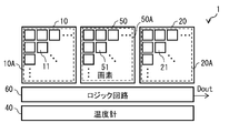
- the light receiving device 1 may further include a medium temperature light receiving unit 50, for example, as shown in FIG.
- the medium temperature light receiving unit 50 has a pixel array 50A.
- the pixel array 50A includes a plurality of pixels 51.
- the pixel arrays 10A, 20A, and 50A correspond to a specific example of the "pixel array" of the present disclosure. At least one of the pixel array 10A and the pixel array 20A and the pixel array 50A are arranged next to each other.
- the three light receiving parts are formed on separate chips (semiconductor substrate (for example, silicon substrate)). You may be.
- the three light receiving parts are, for example, on a common chip (semiconductor substrate (for example, silicon substrate)). It may be formed.
- the thermometer 40 measures the temperatures of the three light receiving units (low temperature light receiving unit 10, high temperature light receiving unit 20, and medium temperature light receiving unit 50), and the measurement result is obtained by the logic circuit 60. Output to.
- the logic circuit 60 is provided instead of the logic circuit 30.
- the logic circuit 60 has a circuit for driving a plurality of pixels 51 in addition to the configuration included in the logic circuit 30.
- the circuit for driving the plurality of pixels 51 is composed of, for example, a circuit common to the pixel drive unit 31, the MUX 32, the signal processing unit 33, the input / output unit 34, and the power supply unit 41.
- the medium temperature light receiving unit 50 has a plurality of pixels 51 arranged two-dimensionally.
- Each pixel 51 includes, for example, an APD (avalanche photodiode) 52 and a transistor electrically connected to the node of the APD 52.
- the transistor is turned on according to the control signal input to the gate, so that the detection signal generated by the APD 52 is output to the signal line DTL.
- the transistor is composed of, for example, a field effect transistor (TFT).
- the control unit 39 controls the output from the logic circuit 30.
- the control unit 39 outputs any of the output signal D1, the output signal D2, and the output signal D3 as the output signal Dout from the logic circuit 30.
- the output signal D3 is data corresponding to the detection signal output from each pixel 51 of the pixel row selected by the pixel drive unit in the medium temperature light receiving unit 50.
- the control unit 39 drives only various circuits for driving any of the three light receiving units (low temperature light receiving unit 10, high temperature light receiving unit 20, medium temperature light receiving unit 50) according to the temperature of the thermometer 40.
- the logic circuit 60 may be controlled so as to do so.
- the control unit 39 has a negative bias voltage only for each APD included in any of the three light receiving units (low temperature light receiving unit 10, high temperature light receiving unit 20, medium temperature light receiving unit 50) according to the temperature of the thermometer 40.
- the power supply unit may be controlled so as to apply.
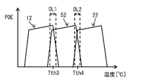
- FIG. 17 shows an example of the temperature dependence of the PDE of APD12, 22, 52.
- APD12 has a high PDE in the low temperature range.
- APD22 has a high PDE in the high temperature region.
- APD52 has a high PDE in the mid-temperature range.
- the high PDE temperature region is relatively distributed on the low temperature side.
- the high PDE temperature region is relatively distributed on the high temperature side.
- the high PDE temperature region is relatively distributed on the medium temperature side.
- the high PDE temperature range of APD12, the high PDE temperature range of APD22, and the high PDE temperature range of APD52 are different from each other. Further, a part of the high PDE temperature region of APD12 and a part of the high PDE temperature region of APD52 overlap each other, and a part of the high PDE temperature region of APD52 and the high PDE temperature of APD22 are overlapped with each other. Part of the area overlaps with each other. As shown in FIG. 17, in the overlapping region OL1 of the high PDE in the APDs 12 and 52, the region on the high temperature side of the high PDE temperature region of the APD12 and the region on the low temperature side of the high PDE temperature region of the APD52 They overlap each other.
- At least one of the impurity concentration contained in the multiplying region, the type of impurities contained in the multiplying region, the thickness of the multiplying region, and the area of the multiplying region are different from each other.
- the high PDE temperature region of APD12, the high PDE temperature region of APD22, and the high PDE temperature region of APD52 are different from each other.
- FIG. 18 shows an example of the switching procedure of the low temperature light receiving unit 10, the high temperature light receiving unit 20, and the medium temperature light receiving unit 50 (output signals D1, D2, D3).
- the control unit 39 determines whether or not the temperature of the thermometer 40 is equal to or higher than a predetermined temperature (threshold value Tth4) in the overlapping region OL2 (step S301).
- a predetermined temperature threshold value Tth4
- the control unit 39 receives light for low temperature by, for example, stopping the operation of various circuits for driving the light receiving unit 10 for low temperature and the light receiving unit 50 for medium temperature. The operation of the unit 10 and the medium temperature light receiving unit 50 is stopped.
- control unit 39 drives the high temperature light receiving unit 20 by, for example, operating various circuits for driving the high temperature light receiving unit 20 (step S302). At this time, the control unit 39 may control the power supply unit so as to apply a negative bias voltage only to each APD 22. As a result, the output signals D1 and D3 are not output from the low temperature light receiving unit 10 and the medium temperature light receiving unit 50, and the output signal D2 is output from the high temperature light receiving unit 20. At this time, the control unit 39 outputs the output signal D2 from the logic circuit 30 as the output signal Dout (step S303).
- step S301 when the temperature of the thermometer 40 is less than the threshold value Tth4, the control unit 39 determines whether or not the temperature of the thermometer 40 is equal to or less than a predetermined temperature (threshold value Tth3) in the overlapping region OL1.
- a predetermined temperature threshold value Tth3
- the control unit 39 stops the operation of various circuits for driving the medium temperature light receiving unit 50 and the high temperature light receiving unit 20, for example, to stop the operation of the medium temperature light receiving unit 20 The operation of the unit 50 and the high temperature light receiving unit 20 is stopped. Further, the control unit 39 drives the low temperature light receiving unit 10 by, for example, operating various circuits for driving the low temperature light receiving unit 10 (step S305).
- control unit 39 may control the power supply unit so as to apply a negative bias voltage only to each APD 12.
- the output signals D2 and D3 are not output from the medium temperature light receiving unit 50 and the high temperature light receiving unit 20, and the output signal D1 is output from the low temperature light receiving unit 10.
- the control unit 39 outputs the output signal D1 from the logic circuit 30 as the output signal Dout (step S306).
- step S304 when the temperature of the thermometer 40 is higher than the threshold value Tth3, the control unit 39 stops the operation of various circuits for driving the low temperature light receiving unit 10 and the high temperature light receiving unit 20, for example, to reduce the temperature.
- the control unit 39 drives the medium temperature light receiving unit 50 by, for example, operating various circuits for driving the medium temperature light receiving unit 50 (step S307).
- the control unit 39 may control the power supply unit so as to apply a negative bias voltage only to each APD 52.
- the control unit 39 outputs the output signal D3 from the logic circuit 30 as the output signal Dout (step S308).
- the control unit 39 executes steps S308 to S308 from step S301 above unless instructed to end the measurement by the light receiving device 1 (step S309).
- the control unit 39 stops the operation of the logic circuit 30, for example, the low temperature light receiving unit 10, the medium temperature light receiving unit 50, and the high temperature light receiving unit 20. (Step S310).
- the plurality of light receiving elements provided for each of the pixels 11, 21, 51 have three types of light receiving elements (APD 12, 22, 52) in which the temperature regions of the PDEs are different from each other and a part of the temperature regions overlap each other. )It is included.
- the APD12 in which the temperature region with high detection efficiency is relatively distributed on the low temperature side is used among the three types of light receiving elements.
- the APD 52 is used, in which the temperature region with high detection efficiency is relatively distributed on the medium temperature side among the three types of light receiving elements.
- the APD22 in which the temperature region with high detection efficiency is relatively distributed on the high temperature side is used among the three types of light receiving elements.
- the decrease in PDE is suppressed at low temperature, medium temperature, and high temperature.
- the guaranteed range of PDE can be expanded as compared with the case where only any one of APD12, APD22 and APD52 is used.
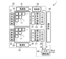
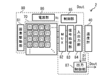
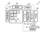
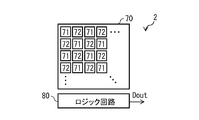
- FIG. 19 shows a schematic configuration example of the light receiving device 2.
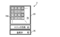
- the light receiving device 2 includes, for example, one light receiving unit 70, a logic circuit 80, and a thermometer 40.
- the light receiving unit 70 has a pixel array 70A.
- the pixel array 70A includes a plurality of pixels 71 and 72.
- the pixel array 70A corresponds to a specific example of the "pixel array" of the present disclosure.
- the logic circuit 80 outputs the output signal Dout generated based on the output signal Dout'from the light receiving unit 70 to the outside. Pixels 71 and 72 will be described in detail later.
- the light receiving unit 70 is formed on a chip 2A separate from the chip provided with the logic circuit 80 and the thermometer 40.
- the chip 2A is configured to include, for example, a silicon substrate.
- the light receiving portion 70 is formed on the silicon substrate (first semiconductor substrate) of the chip 2A.
- the logic circuit 80 is formed on the chip 2B separate from the chip 2A, for example, and the thermometer 40 is formed on the chip 2C separate from the chips 2A and 2B, for example. ing.
- the chip 2A may be bonded on the chip 2B, or the chips 2A, 2B, and 2C may be bonded on a common support substrate.
- the chip 2C may be attached to the back surface of the chip 2B.
- the light receiving unit 70 and the logic circuit 80 may be formed on a common chip 2D, for example, as shown in FIG.
- the chip 2D is configured to include, for example, a silicon substrate, and the light receiving unit 70 and the logic circuit 80 are formed on a common silicon substrate.
- the light receiving unit 70, the logic circuit 80, and the thermometer 40 may be formed on a common chip 2E, for example, as shown in FIG.
- the chip 2E is configured to include, for example, a silicon substrate, and the light receiving unit 70, the logic circuit 80, and the thermometer 40 are formed on a common silicon substrate.
- the thermometer 40 measures the temperature of the light receiving unit 70 and outputs the measurement result to the logic circuit 80.
- the thermometer 40 is composed of, for example, a silicon diode temperature sensor.
- the thermometer 40 may be composed of, for example, a silicon diode temperature sensor, or may be composed of another temperature sensor.
- FIG. 23 shows a schematic configuration example of the logic circuit 80.
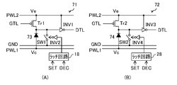
- FIG. 24A shows a circuit configuration example of each pixel 71.
- FIG. 24B shows an example of a circuit configuration of each pixel 72.
- the logic circuit 80 includes, for example, a pixel drive unit 81, a MUX 82, a signal processing unit 83, an input / output unit 84, a control unit 85, and a power supply unit 86.
- the pixel driving unit 81 drives the pixels 71 and 72 in the light receiving unit 70.
- the MUX 82, the signal processing unit 83, and the input / output unit 84 process the output from the light receiving unit 70.
- the output of the input / output unit 84 is referred to as an output signal Dout.
- the power supply unit 86 supplies a predetermined voltage (power supply voltage Vc, Ve) to each of the pixels 71 and 72.
- the light receiving unit 70 has a plurality of pixels 71 and 72 arranged two-dimensionally.
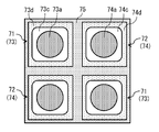
- the plurality of pixels 71, 72 are arranged alternately in the row direction and the column direction in, for example, the pixel array 70A.
- Each pixel 71 includes, for example, an APD (avalanche photodiode) 73 and a transistor Tr1 electrically connected to the node of the APD 73.
- the APD73 corresponds to a specific example of the "first light receiving element" of the present disclosure.
- the transistor Tr1 is turned on according to the control signal input to the gate, so that the detection signal generated by the APD 73 is output to the signal line DTL.
- the transistor Tr1 is composed of, for example, a field effect transistor thin film transistor (TFT).
- Each pixel 72 includes, for example, an APD (avalanche photodiode) 74 and a transistor Tr2 electrically connected to the node of the APD 74.
- APD74 corresponds to a specific example of the "second light receiving element" of the present disclosure.
- the transistor Tr2 is turned on according to the control signal input to the gate, so that the detection signal generated by the APD 74 is output to the signal line DTL.
- the transistor Tr2 is composed of, for example, a field effect transistor thin film transistor (TFT).
- the APDs 73 and 74 are photodiodes (single photon avalanche photodiodes) that amplify the generated charge when incident light is incident and output the detection signal obtained thereby.
- the power supply voltage Vc supplied to the anodes of the APDs 73 and 74 has, for example, a negative bias (negative potential) of about ⁇ 20 V.
- the power supply voltage Ve is supplied to the cathodes of the APDs 73 and 74 via the source and drain of the transistors Tr1 and Tr2.
- the power supply voltage Ve is, for example, a positive potential of about 3 V.
- the transistors Tr1 and Tr2 are constant current sources that operate in the saturation region, and perform passive quenching by acting as a quenching resistor.
- the light receiving unit 70 further has a plurality of signal line DTLs and a plurality of gate line GTLs.
- the light receiving unit 70 further has a plurality of power supply lines PWL1 and PWL2 and a ground line GND.
- the light receiving unit 70 further has a switch element SW1, an inverter INV1, INV2 and a latch circuit 18 in each pixel 71, and has a switch element SW2, an inverter INV3, INV4 and a latch circuit 28 in each pixel 72. ing.
- the signal line DTL is a wiring for reading the detection signal from the APDs 73 and 74.
- the gate line GTL is a wiring for inputting a control signal for on / off control of the transistors Tr1 and Tr2 to the gate of the transistors Tr1 and Tr2.
- the power line PWL1 is a wiring for determining the anode potential of the APDs 73 and 74.
- the power line PWL2 is a wiring for determining the cathode potential of the APDs 73 and 74.
- the gates of the transistors Tr1 and Tr2 are connected to the gate line GTL.
- the source or drain of the transistors Tr1 and Tr2 is connected to the cathode of the APD73 and 74 and the input terminals of the inverters INV1 and INV3.
- the output terminals of the inverters INV1 and INV3 are connected to the signal line DTL.
- the electrodes that are not connected to the cathode are connected to the power supply line PWL2.
- the cathode of APD73,74 is connected to the source or drain of transistors Tr1 and Tr2, and the anode of APD73,74 is connected to the power supply line PWL1.
- the input terminals of the inverters INV2 and INV4 are connected to the latch circuits 18 and 28, and the output terminals of the inverters INV2 and INV4 are connected to the on / off control terminal of the switch element SW1.
- the switch element SW1 is connected in parallel to the APD73.
- the switch element SW2 is connected to the APD 74 in parallel.
- the switch elements SW1 and SW2 turn on and off, for example, the gating control signal which is the output of the latch circuits 18 and 28 according to the gating inverting signal inverted by the inverters INV2 and INV4.
- the latch circuits 18 and 28 provide a gating control signal for controlling the pixels 71 and 72 to either active pixels or inactive pixels based on the trigger signal SET supplied from the pixel drive unit 81 and the address data DEC. It is supplied to the inverters INV2 and INV4.
- the inverters INV2 and INV4 generate a gating inversion signal in which the gating control signal is inverted and supply it to the switch elements SW1 and SW2.
- the trigger signal SET is a timing signal indicating the timing for switching the gating control signal
- the address data DEC is a pixel set as an active pixel among a plurality of pixels 71 and 72 arranged in a matrix in the pixel array 70A. It is the data which shows the address of.
- the trigger signal SET and the address data DEC are supplied from the pixel drive unit 81.
- the latch circuits 18 and 28 read the address data DEC at a predetermined timing indicated by the trigger signal SET. Then, when the pixel addresses indicated by the address data DEC include their own (pixels 71, 72) pixel addresses, the latch circuits 18 and 28 set their own pixels 71 and 72 as active pixels. The gating control signal of Hi (1) is output. On the other hand, when the pixel address indicated by the address data DEC does not include the pixel address of oneself (pixels 71, 72), Lo (0) for setting one's own pixels 71, 72 as an inactive pixel. Outputs a gating control signal.
- the Lo (0) gating inversion signal inverted by the inverters INV2 and INV4 is supplied to the switch elements SW1 and SW2.
- the gating inversion signal of Hi (1) is supplied to the switch elements SW1 and SW2. Therefore, the switch elements SW1 and SW2 are turned off (disconnected) when the pixels 71 and 72 are set as active pixels, and turned on (connected) when the pixels 71 and 72 are set as inactive pixels.
- the inverters INV2 and INV4 output a Hi detection signal when the cathode voltage as an input signal is Lo, and output a Lo detection signal when the cathode voltage is Hi.
- the inverters INV2 and INV4 are output units that output the incident of photons on the APDs 73 and 74 as a detection signal.
- each pixel 71, 72 will be described.
- the switch elements SW1 and SW2 are set to off as described above.
- the power supply voltage Ve is supplied to the cathode of the APD73 and 74 and the power supply voltages Va and Vb are supplied to the anode, a reverse voltage larger than the yield voltage VBD is applied to the APD73 and 74 to cause the APD73 and 74. Is set to Geiger mode. In this state, the cathode voltage VS of the APDs 73 and 74 is the same as the power supply voltage Ve, for example, at time t0 in FIG.
- the cathode voltage VS of APD73,74 becomes lower than 0V
- the anode-cathode voltage of APD73,74 becomes lower than the yield voltage VBD, so that the avalanche amplification is stopped.
- the current generated by the avalanche amplification flows through the transistors Tr1 and Tr2 to generate a voltage drop, and the cathode voltage VS becomes lower than the breakdown voltage VBD as the generated voltage drop causes the avalanche amplification.
- the operation of stopping is the quenching operation.
- the inverters INV2 and INV4 output the Lo detection signal PFout when the cathode voltage VS, which is the input voltage, is equal to or higher than the predetermined threshold voltage Vth, and the Hi detection signal PFout when the cathode voltage VS is less than the predetermined threshold voltage Vth. Is output. Therefore, when a photon is incident on the APDs 73 and 74, an avalanche multiplication occurs, the cathode voltage VS decreases, and the threshold voltage Vth falls below the threshold voltage Vth, the detection signal PFout is inverted from a low level to a high level. On the other hand, when the avalanche multiplication of APD73 and 74 converges, the cathode voltage VS rises, and becomes the threshold voltage Vth or more, the detection signal PFout is inverted from the high level to the low level.
- the gating inversion signal of Hi (1) is supplied to the switch elements SW1 and SW2, and the switch elements SW1 and SW2 are turned on.
- the switch elements SW1 and SW2 are turned on, the cathode voltage VS of the APDs 73 and 74 becomes 0V.
- the voltage between the anode and the cathode of the APDs 73 and 74 becomes equal to or less than the yield voltage VBD, so that even if photons enter the APDs 73 and 74, they do not react.
- the pixel drive unit 81 is composed of, for example, a shift register, an address decoder, or the like, and drives each pixel 71, 72, for example, in row units.
- the detection signal output from each pixel 71, 72 of the pixel row selectively scanned by the pixel drive unit 81 is supplied to the MUX 82 via each signal line DTL.
- the MUX82 selects the output from the active pixel according to the switching between the active pixel and the inactive pixel in the pixel array 70A. Then, the MUX 82 outputs the pixel signal input from the selected active pixel to the signal processing unit 83.
- the signal processing unit 83 is, for example, a time measuring unit.
- the time measuring unit is based on the pixel signal of the active pixel supplied from the MUX82 and the light emission timing signal indicating the light emission timing of the light source (described later), from the light source emitting light to the active pixel receiving light. Generate a count value corresponding to the time of.
- the time measurement unit is also called a TDC (Time to Digital Converter).
- the light emission timing signal is supplied from the outside via the input / output unit 84.
- the signal processing unit 83 may be a counter unit.
- the counter unit counts, for example, the number of detection signals input from the MUX 82 for a predetermined period, and outputs the count value for each pixel obtained thereby.
- the power supply unit 86 is connected to each power supply line PWL1 connected to each pixel 71 and 72, and a negative bias voltage (power supply voltage Vc) is applied to each power supply line PWL1 to which each pixel 71 and 72 is connected.
- the power supply unit 86 is further connected to each power supply line PWL2 connected to each pixel 71 and 72, and a predetermined voltage (power supply voltage Ve) is applied to each power supply line PWL2 to which each pixel 71 and 72 is connected.
- the power supply voltage Vc preferably has a value that maximizes the PDEs of APD73 and 74.
- the input / output unit 84 receives the output signal D1 obtained from each pixel 71 and the output signal D2 obtained from each pixel 72 from the output signal Dout'output from the signal processing unit 83 according to the control from the control unit 85. Extract one.
- the input / output unit 84 outputs the signal obtained by the extraction as an output signal Dout.
- the input / output unit 84 selects either the output signal D1 or the output signal D2 according to the temperature of the thermometer 40.
- the signal processing unit 83 is a time measuring unit
- the input / output unit 84 supplies the light emission timing signal supplied from the control unit 85 to the pixel drive unit 81 and the signal processing unit 83.
- the control unit 85 receives a clock or the like given from the outside, and also outputs data such as internal information of the light receiving device 2.
- the control unit 85 further has a timing generator that generates various timing signals, and based on the various timing signals generated by the timing generator, the pixel drive unit 81, the MUX 82, the signal processing unit 83, and the input / output unit Drive control of the 84 and the power supply unit 86 and the like is performed.
- the control unit 85 controls the output from the logic circuit 80.
- the control unit 85 outputs an output signal Dout including either the output signal D1 or the output signal D2 from the input / output unit 84.
- the control unit 85 instructs the input / output unit 84 whether to select the output signal D1 or the output signal D2 according to the temperature of the thermometer 40.
- FIG. 25 shows an example of cross-sectional configuration of each pixel 71 for low temperature.
- Each pixel 71 has, for example, an n-type semiconductor region 73a and a p-type semiconductor region 73b.
- the p-type semiconductor region 73b is formed in contact with the lower portion of the n-type semiconductor region 73a.
- the n-type semiconductor region 73a and the p-type semiconductor region 73b are formed in the well layer 73c.
- the well layer 73c may be an n-type semiconductor layer or a p-type semiconductor layer.
- the well layer 73c is preferably an n-type semiconductor layer or a p-type semiconductor layer having a low impurity concentration of 1 ⁇ 10 14 cm -3 or less, for example. In this case, the well layer 73c is likely to be depleted, and the PDE of the APD73 can be improved.
- the n-type semiconductor region 73a is, for example, Si (silicon) and is an n-type semiconductor region having a high impurity concentration.
- the p-type semiconductor region 73b is, for example, Si (silicon) and is a p-type semiconductor region having a high impurity concentration.
- the p-type semiconductor region 73b constitutes a pn junction at the interface with the n-type semiconductor region 73a.
- the region including the pn junction is the high electric field region, and the n-type semiconductor region 73a is the photoelectric conversion region.
- the p-type semiconductor region 73b has a multiplication region that avalanche-amplifies the carriers generated by the incident light to be detected.
- the p-type semiconductor region 73b is preferably depleted. In this case, the PDE of the APD73 can be improved.
- the n-type semiconductor region 73a functions as a cathode and is connected to a circuit via a contact 78.
- the anode 73d with respect to the cathode is in the same layer as the n-type semiconductor region 73a, and is formed between the n-type semiconductor region 73a and the separation region 75.
- the anode 73d is connected to the circuit via the contact 79.
- a separation region 75 for separating two APDs 73, 74 adjacent to each other is formed, and a hole accumulation region 73e is formed between the separation region 75 and the well layer 73c.
- the hole storage region 73e is formed below the anode 73d and is formed in a state of being electrically connected to the anode 73d. Further, the hole accumulation region 73e is formed between the well layer 73c and the separation region 75. Further, the hole accumulation region 73e is also formed in contact with the lower part of the well layer 73c.
- the hole accumulation region 73e is formed in a portion where different materials are in contact with each other. In the example shown in FIG.
- the separation region 75 is made of, for example, a silicon oxide film, and is made of a material different from that of the well layer 73c.
- the hole accumulation region 73e is formed in order to suppress the dark current generated at the interface.
- the hole storage region 73e can be formed as, for example, a p-type semiconductor region.
- the separation region 75 is formed between two APDs 73 and 74 adjacent to each other, and separates the APDs 73 and 74. That is, the separation region 75 is formed so that a multiplication region is formed one-to-one with each of the APDs 73 and 74.
- the separation region 75 is formed in a two-dimensional grid pattern so as to completely surround each of the APDs 73 and 74.
- the separation region 75 is formed so as to penetrate from the upper surface side to the lower surface side of the well layer 73c in the stacking direction.
- the separation region 75 may have a configuration in which only a part of the separation region 75 penetrates and is inserted halfway through the substrate, other than a configuration in which the separation region 75 penetrates completely from the upper surface side to the lower surface side.
- FIG. 26 shows an example of cross-sectional configuration of each pixel 72 for high temperature.
- Each pixel 72 has, for example, an n-type semiconductor region 74a and a p-type semiconductor region 74b.
- the p-type semiconductor region 74b is formed in contact with the lower portion of the n-type semiconductor region 74a.
- the n-type semiconductor region 74a and the p-type semiconductor region 74b are formed in the well layer 74c.
- the well layer 74c may be an n-type semiconductor layer or a p-type semiconductor layer.
- the well layer 74c is preferably an n-type semiconductor layer or a p-type semiconductor layer having a low impurity concentration of 1 ⁇ 10 14 cm -3 or less, for example. In this case, the well layer 74c is easily depleted, and the PDE of the APD 74 can be improved.
- the n-type semiconductor region 74a is, for example, Si (silicon) and is an n-type semiconductor region having a high impurity concentration.
- the p-type semiconductor region 74b is, for example, Si (silicon) and is a p-type semiconductor region having a high impurity concentration.
- the p-type semiconductor region 74b constitutes a pn junction at the interface with the n-type semiconductor region 74a.
- the region including the pn junction is the high electric field region, and the n-type semiconductor region 74a is the photoelectric conversion region.
- the p-type semiconductor region 74b has a multiplication region that avalanche-amplifies the carriers generated by the incident light to be detected.
- the p-type semiconductor region 74b is preferably depleted. In this case, the PDE of the APD 74 can be improved.
- the n-type semiconductor region 74a functions as a cathode and is connected to a circuit via a contact 78.
- the anode 74d with respect to the cathode is in the same layer as the n-type semiconductor region 74a, and is formed between the n-type semiconductor region 74a and the separation region 75.
- the anode 73d is connected to the circuit via the contact 79.
- a separation region 75 for separating two APDs 73 and 74 adjacent to each other is formed, and a hole accumulation region 74e is formed between the separation region 75 and the well layer 74c.
- the hole storage region 74e is formed below the anode 74d and is formed in a state of being electrically connected to the anode 74d. Further, the hole accumulation region 74e is formed between the well layer 74c and the separation region 75. Further, the hole accumulation region 74e is also formed in contact with the lower part of the well layer 74c.
- the hole accumulation region 74e is formed in a portion where different materials are in contact with each other. In the example shown in FIG.
- the separation region 75 is made of, for example, a silicon oxide film, and is made of a material different from that of the well layer 74c.
- the hole accumulation region 74e is formed in order to suppress the dark current generated at the interface.
- the hole storage region 74e can be formed as, for example, a p-type semiconductor region.
- FIG. 27 shows an example of the plan configuration of the light receiving unit 70.
- FIG. 27 shows an example in which four 2 ⁇ 2 APDs (two APD73s and two APD74s) are arranged.
- the APDs 73 and 74 are separated from each other by the separation regions 75 formed in a grid pattern.
- Anodes 73d and 74d are formed inside the separation region 75.
- N-type semiconductor regions 73a and 74a are formed in the central portion of the APDs 73 and 74, and well layers 73c and 74c are formed between the anodes 73d and 74d and the n-type semiconductor regions 73a and 74a. ..
- the n-type semiconductor regions 73a and 74a have, for example, a rectangular shape.
- the planar shape of the n-type semiconductor regions 73a and 74a is not limited to a quadrangular shape, and may be, for example, a circular shape.
- the n-type semiconductor regions 73a and 74a are rectangular, the area of the multiplication region can be secured widely, so that the PDE can be improved.
- the n-type semiconductor regions 73a and 74a are circular, the electric field concentration in the APDs 73 and 74 can be suppressed, and an unintended breakdown can be reduced.
- FIG. 28 shows an example of the temperature dependence of the PDEs of APD73 and 74.
- APD73 has a high PDE in the low temperature range.
- APD74 has a high PDE in a high temperature region.
- the high PDE temperature region is relatively distributed on the low temperature side.
- the high PDE temperature region is relatively distributed on the high temperature side.
- the high PDE temperature region of the APD73 and the high PDE temperature region of the APD74 are different from each other, and a part of the high PDE temperature region of the APD73 and a part of the high PDE temperature region of the APD74 are They overlap each other.
- the “high PDE temperature region” refers to a temperature region larger than half the peak value in the PDE temperature distribution. As shown in FIG. 28, in the overlapping region OL of the high PDE in the APD73 and 74, the region on the high temperature side of the high PDE temperature region of the APD73 and the region on the low temperature side of the high PDE temperature region of the APD74 are located. They overlap each other.
- At least one of the thickness of the type semiconductor regions 73b and 74b) and the area of the multiplication region (p-type semiconductor regions 73b and 74b) are different from each other.
- the high PDE temperature region of the APD73 and the high PDE temperature region of the APD74 are different from each other.
- FIG. 29 shows an example of the switching procedure of the output signals D1 and D2.
- the control unit 85 determines whether or not the temperature of the thermometer 40 is equal to or higher than a predetermined temperature (threshold value Tth) in the overlapping region OL (step S401). When the temperature of the thermometer 40 is equal to or higher than the threshold value Tth, the control unit 85 outputs a control signal instructing the selection of the output signal D2 to the input / output unit 84.
- the input / output unit 84 extracts the output signal D2 from the output signal Dout'output from the signal processing unit 83 based on the control signal from the control unit 85 (step S402).
- the input / output unit 84 outputs the output signal D2 obtained by extraction as an output signal Dout (step S403).
- step S401 when the temperature of the thermometer 40 is less than the threshold value Tth, the control unit 85 outputs a control signal instructing the selection of the output signal D1 to the input / output unit 84.
- the input / output unit 84 extracts the output signal D1 from the output signal Dout'output from the signal processing unit 83 based on the control signal from the control unit 85 (step S404).
- the input / output unit 84 outputs the output signal D2 obtained by extraction as an output signal Dout (step S405).
- the control unit 85 executes steps S401 to S405 described above (step S406) unless instructed to end the measurement by the light receiving device 2.
- the control unit 85 stops the operation of the light receiving unit 70, for example, by stopping the operation of the logic circuit 80 (step S407).
- control unit 85 may execute the following switching procedure.
- FIG. 31 shows an example of the switching procedure of the output signals D1 and D2.
- the control unit 85 determines whether or not the temperature of the thermometer 40 is equal to or higher than the upper limit temperature (threshold value Tth2) of the overlapping region OL (step S501). When the temperature of the thermometer 40 is equal to or higher than the threshold value Tth2, the control unit 85 outputs a control signal instructing the selection of the output signal D2 to the input / output unit 84.
- the input / output unit 84 extracts the output signal D2 from the output signal Dout'output from the signal processing unit 83 based on the control signal from the control unit 85 (step S502).
- the input / output unit 84 outputs the output signal D2 obtained by extraction as an output signal Dout (step S503).
- step S501 when the temperature of the thermometer 40 is less than the threshold value Tth2, the control unit 85 determines whether or not the temperature of the thermometer 40 is equal to or less than the threshold value Tth1 (step S504).
- the control unit 85 outputs a control signal instructing the selection of the output signal D1 to the input / output unit 84.
- the input / output unit 84 extracts the output signal D1 from the output signal Dout'output from the signal processing unit 83 based on the control signal from the control unit 85 (step S505).
- the input / output unit 84 outputs the output signal D1 obtained by extraction as an output signal Dout (step S506).
- step S504 when the temperature of the thermometer 40 is larger than the threshold value Tth1, the control unit 85 outputs a control signal instructing the selection of the output signals D1 and D2 to the input / output unit 84.
- the input / output unit 84 extracts output signals D1 and D2 from the output signal Dout'output from the signal processing unit 83 based on the control signal from the control unit 85 (step S507).
- the input / output unit 84 outputs the output signals D1 and D2 obtained by the extraction as the output signal Dout (step S508).
- the control unit 85 executes steps S501 to S508 above (step S509) unless instructed to end the measurement by the light receiving device 2.
- the control unit 85 stops the operation of the light receiving unit 70, for example, by stopping the operation of the logic circuit 80 (step S510).
- the control unit 85 controls the power supply unit 86 so as not to apply a negative bias voltage to the APDs 73 and 74, for example.
- control unit 85 may always drive the light receiving unit 70 regardless of the temperature of the thermometer 40, and output a signal including the output signals D1 and D2 from the logic circuit 80 as the output signal Dout.
- the plurality of light receiving elements provided for each of the pixels 71 and 72 include two types of light receiving elements (APD73, 74) in which the temperature regions of the PDEs are different from each other and a part of the temperature regions overlap each other. It has been.
- the APD73 in which the temperature region with high detection efficiency is relatively distributed on the low temperature side is used among the two types of light receiving elements, and when the charge is read out at a high temperature.
- the APD74 in which the temperature region with high detection efficiency is relatively distributed on the high temperature side among the two types of light receiving elements, the decrease in PDE is suppressed at both low temperature and high temperature.
- the guaranteed range of PDE can be expanded as compared with the case where only one of APD73 and APD74 is used.
- a plurality of APDs 73 and 74 are alternately arranged in the pixel array 70A.
- the distance between the APD73 and the APD74 located at the common coordinates can be shortened as compared with the case where the plurality of APD73s and the plurality of APD74s are formed in separate regions.
- the optical axes of the plurality of APD73s and the optical axes of the plurality of APD74s can be brought close to each other, it becomes easy to design an optical system that guides the incident light to the pixel array 70A.
- a power supply unit 86 for applying a negative bias voltage Vc to each of the APDs 73 and 74 is provided. Thereby, the PDE of each APD73,74 can be improved.
- a negative bias voltage Vc common to the APDs 73 and 74 is applied by the power supply unit 86.
- the light receiving device 2 can be miniaturized as compared with the case where different negative bias voltages are applied to the APDs 73 and 74.
- FIG. 32 shows a schematic configuration example of the light receiving device 3.
- the light receiving device 3 includes, for example, one light receiving unit 110, a logic circuit 120, and a thermometer 130.
- the light receiving unit 110 has a pixel array 110A.
- the pixel array 110A includes a plurality of pixels Px.
- the pixel array 110A corresponds to a specific example of the "pixel array" of the present disclosure.
- the logic circuit 120 outputs the output signal Dout generated based on the output from the light receiving unit 110 to the outside.
- Each pixel Px is configured to include a low-temperature sub-pixel Pa and a high-temperature sub-pixel Pb. The sub-pixels Pa and Pb will be described in detail later.
- the light receiving unit 110 is formed on a chip 3A separate from the chip provided with the logic circuit 120 and the thermometer 130.
- the chip 3A is configured to include, for example, a silicon substrate.
- the light receiving unit 110 is formed on the silicon substrate (semiconductor substrate) of the chip 3A.
- the logic circuit 120 is formed on the chip 3B separate from the chip 3A, for example, and the thermometer 130 is formed on the chip 3C separate from the chips 3A and 3B, for example. ing.
- the chip 3A may be bonded on the chip 3B, or the chips 3A, 3B, and 3C may be bonded on a common support substrate.
- the chip 3C may be attached to the back surface of the chip 3B.
- the light receiving unit 110 and the logic circuit 120 may be formed on a common chip 3D, for example, as shown in FIG. 34.
- the chip 3D is configured to include, for example, a silicon substrate, and the light receiving unit 110 and the logic circuit 120 are formed on a common silicon substrate.
- the light receiving unit 110, the logic circuit 120, and the thermometer 130 may be formed on a common chip 3E, for example, as shown in FIG. 35.
- the chip 3E is configured to include, for example, a silicon substrate, and the light receiving unit 110, the logic circuit 120, and the thermometer 130 are formed on a common silicon substrate.
- the thermometer 130 measures the temperature of the light receiving unit 110 and outputs the measurement result to the logic circuit 120.
- the thermometer 130 is composed of, for example, a silicon diode temperature sensor.
- the thermometer 130 may be composed of, for example, a silicon diode temperature sensor, or may be composed of another temperature sensor.
- FIG. 36 shows a schematic configuration example of the logic circuit 120.
- FIG. 37A shows an example of a circuit configuration of each pixel Pa.
- FIG. 37B shows an example of a circuit configuration of each pixel Pb.
- the logic circuit 120 includes, for example, a pixel drive unit 121, a MUX 122, a signal processing unit 123, an input / output unit 124, a control unit 125, and a power supply unit 126.
- the pixel driving unit 121 drives each pixel Px in the light receiving unit 110.
- the MUX 122, the signal processing unit 123, and the input / output unit 124 process the output from the light receiving unit 110.
- the output of the input / output unit 124 is referred to as an output signal Dout.
- the power supply unit 126 supplies a predetermined voltage (power supply voltage Va, Vb, Ve) to each pixel Px.
- the light receiving unit 110 has sub-pixels Pa and Pb for each pixel Px.
- the sub-pixel Pa includes, for example, an APD (avalanche photodiode) 111 and a transistor Tr1 electrically connected to the node of the APD 111.
- APD111 corresponds to a specific example of the "first light receiving element" of the present disclosure.
- the transistor Tr1 is turned on according to the control signal input to the gate, so that the detection signal generated by the APD 111 is output to the signal line DTL.
- the transistor Tr1 is composed of, for example, a field effect transistor thin film transistor (TFT).
- the sub-pixel Pb includes, for example, an APD (avalanche photodiode) 112 and a transistor Tr2 electrically connected to the node of the APD 112.
- the APD112 corresponds to a specific example of the "second light receiving element" of the present disclosure.
- the transistor Tr2 is turned on according to the control signal input to the gate, so that the detection signal generated by the APD 112 is output to the signal line DTL.
- the transistor Tr2 is composed of, for example, a field effect transistor thin film transistor (TFT).
- the APDs 111 and 112 are photodiodes (single photon avalanche photodiodes) that amplify the electric charge generated when incident light is incident and output the detection signal obtained thereby.
- the power supply voltage Va supplied to the anode of the APD 111 is, for example, a negative bias (negative potential) of about ⁇ 20 V.
- the power supply voltage Vb supplied to the anode of the APD 112 has, for example, a negative bias (negative potential) of about ⁇ 20 V.
- the power supply voltage Va and the power supply voltage Vb may be equal to each other or different from each other.
- a power supply voltage Ve is supplied to the cathodes of the APDs 111 and 112 via the source and drain of the transistors Tr1 and Tr2.
- the power supply voltage Ve is, for example, a positive potential of about 3 V.
- the transistors Tr1 and Tr2 are constant current sources that operate in the saturation region, and perform passive quenching by acting as a quenching
- the light receiving unit 110 further has a plurality of signal line DTLs and a plurality of gate line GTLs.
- the light receiving unit 110 further has a plurality of power supply lines PWL1 and PWL2 and a ground line GND.
- the light receiving unit 110 further has a switch element SW1, an inverter INV1, INV2 and a latch circuit 18 in the sub-pixel Pa, and has a switch element SW2, an inverter INV3, INV4 and a latch circuit 28 in the sub-pixel Pb. ing.
- the signal line DTL is wiring for reading the detection signal from the APDs 111 and 112.
- the gate line GTL is a wiring for inputting a control signal for on / off control of the transistors Tr1 and Tr2 to the gate of the transistors Tr1 and Tr2.
- the power line PWL1 is a wiring for determining the anode potentials of the APDs 111 and 112.
- the power line PWL2 is a wiring for determining the cathode potential of the APDs 111 and 112.
- the gate of the transistors Tr1 and Tr2 is connected to the gate line GTL, the source or drain of the transistors Tr1 and Tr2 is connected to the node of APD111 and 112, and the electrode of the source and drain of the transistors Tr1 and Tr2 which is not connected to the node signals. It is connected to the line DTL.
- the nodes of APD111 and 112 are connected to the source or drain of transistors Tr1 and Tr2, and the anodes of APD111 and 112 are connected to the power supply line PWL1.
- the input terminals of the inverters INV2 and INV4 are connected to the latch circuits 18 and 28, and the output terminals of the inverters INV2 and INV4 are connected to the on / off control terminal of the switch element SW1.
- the switch element SW1 is connected in parallel to the APDs 111 and 112.
- the switch elements SW1 and SW2 turn on and off, for example, the gating control signal which is the output of the latch circuits 18 and 28 according to the gating inverting signal inverted by the inverters INV2 and INV4.
- the latch circuits 18 and 28 are gating control signals that control the sub-pixels Pa and Pb to either active pixels or inactive pixels based on the trigger signal SET supplied from the pixel drive unit 121 and the address data DEC. Is supplied to the inverters INV2 and INV4.
- the inverters INV2 and INV4 generate a gating inversion signal in which the gating control signal is inverted and supply it to the switch elements SW1 and SW2.
- the trigger signal SET is a timing signal indicating the timing for switching the gating control signal
- the address data DEC is set as the active pixel among the plurality of sub-pixels Pa and Pb arranged in a matrix in the pixel array 110A. This is data indicating the pixel address.
- the trigger signal SET and the address data DEC are supplied from the pixel drive unit 121.
- the latch circuits 18 and 28 read the address data DEC at a predetermined timing indicated by the trigger signal SET. Then, when the pixel addresses indicated by the address data DEC include the pixel addresses of their own (sub-pixels Pa, Pb), the latch circuits 18 and 28 set their own sub-pixels Pa and Pb as active pixels. The Gating control signal of Hi (1) is output. On the other hand, when the pixel address indicated by the address data DEC does not include the pixel address of its own (sub-pixels Pa, Pb), Lo (0) for setting its own sub-pixels Pa, Pb as inactive pixels. ) Gating control signal is output.
- the Lo (0) gating inversion signal inverted by the inverters INV2 and INV4 is supplied to the switch elements SW1 and SW2.
- the gating inversion signal of Hi (1) is supplied to the switch elements SW1 and SW2. Therefore, the switch elements SW1 and SW2 are turned off (disconnected) when the sub-pixels Pa and Pb are set as active pixels, and turned on (connected) when they are set as inactive pixels.
- the inverters INV2 and INV4 output a Hi detection signal when the cathode voltage as an input signal is Lo, and output a Lo detection signal when the cathode voltage is Hi.
- the inverters INV2 and INV4 are output units that output the incident of photons on the APDs 12 and 22 as a detection signal.
- each sub-pixel Pa and Pb are active pixels, the switch elements SW1 and SW2 are set to off as described above.
- the power supply voltage Ve is supplied to the cathodes of the APDs 111 and 112 and the power supply voltages Va and Vb are supplied to the anodes, a reverse voltage larger than the yield voltage VBD is applied to the APDs 111 and 112, whereby the APDs 111 and 112 Is set to Geiger mode.
- the cathode voltage VS of the APDs 111 and 112 is the same as the power supply voltage Ve, for example, at time t0 in FIG.
- the cathode voltage VS of APD111,112 becomes lower than 0V
- the anode-cathode voltage of APD111, 112 becomes lower than the yield voltage VBD, so that the avalanche amplification is stopped.
- the current generated by the avalanche amplification flows through the transistors Tr1 and Tr2 to generate a voltage drop, and the cathode voltage VS becomes lower than the breakdown voltage VBD as the generated voltage drop causes the avalanche amplification.
- the operation of stopping is the quenching operation.
- the inverters INV2 and INV4 output the Lo detection signal PFout when the cathode voltage VS, which is the input voltage, is equal to or higher than the predetermined threshold voltage Vth, and the Hi detection signal PFout when the cathode voltage VS is less than the predetermined threshold voltage Vth. Is output. Therefore, when a photon is incident on the APDs 111 and 112, an avalanche multiplication occurs, the cathode voltage VS decreases, and the threshold voltage Vth falls below the threshold voltage Vth, the detection signal PFout is inverted from a low level to a high level. On the other hand, when the avalanche multiplication of APD111 and 112 converges, the cathode voltage VS rises, and becomes the threshold voltage Vth or more, the detection signal PFout is inverted from the high level to the low level.
- the gating inversion signal of Hi (1) is supplied to the switch elements SW1 and SW2, and the switch elements SW1 and SW2 are turned on.
- the switch elements SW1 and SW2 are turned on, the cathode voltage VS of the APDs 111 and 112 becomes 0V.
- the voltage between the anode and the cathode of the APDs 111 and 112 becomes equal to or less than the yield voltage VBD, so that even if photons enter the APDs 111 and 112, they do not react.
- the pixel drive unit 121 is configured by, for example, a shift register, an address decoder, or the like, and drives each sub-pixel Pa, Pb, for example, in row units.
- the detection signals output from the sub-pixels Pa and Pb of the pixel row selectively scanned by the pixel drive unit 121 are supplied to the MUX 122 via each signal line DTL.
- the MUX 122 selects the output from the active pixel according to the switching between the active pixel and the inactive pixel in the pixel array 110A. Then, the MUX 122 outputs the pixel signal input from the selected active pixel to the signal processing unit 123.
- the signal processing unit 123 is, for example, a time measuring unit.
- the time measuring unit is based on the pixel signal of the active pixel supplied from the MUX 122 and the light emission timing signal indicating the light emission timing of the light source (described later), from the light source emitting light to the active pixel receiving light. Generate a count value corresponding to the time of.
- the time measurement unit is also called a TDC (Time to Digital Converter).
- the light emission timing signal is supplied from the outside via the input / output unit 124.
- the signal processing unit 123 may be a counter unit.
- the counter unit counts, for example, the number of detection signals input from the MUX 122 for a predetermined period, and outputs the count value for each pixel obtained thereby.
- the power supply unit 126 is connected to each power supply line PWL1 connected to each sub-pixel Pa, and applies a negative bias voltage (power supply voltage Va) to each power supply line PWL1 connected to each sub-pixel Pa.
- the power supply unit 126 is further connected to each power supply line PWL2 connected to each sub-pixel Pa, and applies a predetermined voltage (power supply voltage Ve) to each power supply line PWL2 connected to each sub-pixel Pa.
- the power supply unit 126 is connected to each power supply line PWL1 connected to each sub-pixel Pb, and applies a negative bias voltage (power supply voltage Vb) to each power supply line PWL1 connected to each sub-pixel Pb.
- the power supply unit 126 is further connected to each power supply line PWL2 connected to each sub-pixel Pb, and applies a predetermined voltage (power supply voltage Ve) to each power supply line PWL2 connected to each sub-pixel Pb.
- the power supply voltage Va preferably has a value that maximizes the PDE of the APD111.
- the power supply voltage Vb preferably has a value that maximizes the PDE of the APD112.
- the input / output unit 124 receives the output signal D1 obtained from each sub-pixel Pa and the output signal obtained from each sub-pixel Pb from the output signal Dout'output from the signal processing unit 123 according to the control from the control unit 125. Extract any of D2.
- the input / output unit 124 outputs the signal obtained by the extraction as an output signal Dout.
- the input / output unit 124 selects either the output signal D1 or the output signal D2 according to the temperature of the thermometer 130.
- the signal processing unit 123 is a time measuring unit
- the input / output unit 124 supplies the light emission timing signal supplied from the control unit 125 to the pixel driving unit 121 and the signal processing unit 123.
- the control unit 125 receives a clock or the like given from the outside, and also outputs data such as internal information of the light receiving device 3.
- the control unit 125 further has a timing generator that generates various timing signals, and based on the various timing signals generated by the timing generator, the pixel drive unit 121, the MUX 122, the signal processing unit 123, and the input / output unit Drive control of 124 and the power supply unit 126 is performed.
- the control unit 125 causes the input / output unit 124 to output an output signal Dout including either the output signal D1 or the output signal D2.
- the control unit 125 instructs the input / output unit 124 whether to select the output signal D1 or the output signal D2 according to the temperature of the thermometer 130.
- FIG. 38 shows an example of cross-sectional configuration of each pixel Px.
- Each pixel Px has, for example, an n-type semiconductor region 113a and a p-type semiconductor region 113b, 113f.
- the p-type semiconductor regions 113b and 113f are formed in contact with the lower portion of the n-type semiconductor region 113a.
- the p-type semiconductor region 113b belongs to the APD111 of the sub-pixel Pa
- the p-type semiconductor region 113f belongs to the APD112 of the sub-pixel Pb.
- the n-type semiconductor region 113a and the p-type semiconductor region 113b are formed in the well layer 113c belonging to the APD 111 of the sub-pixel Pa.
- the n-type semiconductor region 113a and the p-type semiconductor region 113f are formed in the well layer 113g belonging to the APD 112 of the sub-pixel Pb.
- the well layers 113c and 113g may be an n-type semiconductor layer or a p-type semiconductor layer.
- the well layers 113c and 113 g are preferably an n-type semiconductor layer or a p-type semiconductor layer having a low impurity concentration of 1 ⁇ 10 14 cm -3 or less, for example. In this case, the well layers 113c and 113g are easily depleted, and the PDE of APD111 and 112 can be improved.
- the n-type semiconductor region 113a is, for example, Si (silicon) and is an n-type semiconductor region having a high impurity concentration.
- the p-type semiconductor regions 113b and 113f are, for example, Si (silicon) and are p-type semiconductor regions having a high impurity concentration.
- the p-type semiconductor regions 113b and 113f form a pn junction at the interface with the n-type semiconductor region 113a.
- the region including the pn junction is the high electric field region, and the n-type semiconductor region 113a is the photoelectric conversion region.
- the p-type semiconductor regions 113b and 113f have a multiplication region that avalanche-amplifies the carriers generated by the incident light to be detected.
- the p-type semiconductor regions 113b and 113f are preferably depleted. In this case, the PDE of APD111 and 112 can be improved.
- the n-type semiconductor region 113a functions as a cathode and is connected to a circuit via a contact 116a.
- the anode 113d belonging to the APD 111 of the sub-pixel Pa with respect to the cathode is in the same layer as the n-type semiconductor region 113a, and is formed between the n-type semiconductor region 113a and the separation region 114.
- the anode 113d is connected to the circuit via the contact 116b.
- the anode 113h belonging to the APD 112 of the sub-pixel Pb with respect to the cathode is in the same layer as the n-type semiconductor region 113a, and is formed between the n-type semiconductor region 113a and the separation region 114.
- the anode 113h is connected to the circuit via the contact 116c.
- a separation region 114 for separating each pixel Px is formed.
- a hole accumulation region 113e is formed between the separation region 114 and the well layer 113c.
- a hole accumulation region 113i is formed between the separation region 114 and the well layer 113g.
- the hole storage region 113e is formed below the anode 113d and is formed in a state of being electrically connected to the anode 113d.
- the hole storage region 113i is formed below the anode 113h and is formed in a state of being electrically connected to the anode 113h.
- the hole accumulation region 113e is formed between the well layer 113c and the separation region 114. Further, the hole accumulation region 113e is also formed in contact with the lower part of the well layer 113c.
- the hole accumulation region 113i is formed between the well layer 113g and the separation region 114. Further, the hole accumulation region 113i is also formed in contact with the lower part of the well layer 113g.
- the hole accumulation regions 113e and 113i are formed in portions where different materials are in contact with each other.
- the separation region 114 is made of, for example, a silicon oxide film, and is made of a material different from the well layers 113c and 113g.
- the hole storage regions 113e and 113i are formed in order to suppress the dark current generated at the interface.
- the hole storage regions 113e and 113i can be formed as, for example, a p-type semiconductor region.
- a separation region 115 for separating the sub-pixels Pa and Pb is formed.
- the separation region 115 is formed in contact with the lower portion of the n-type semiconductor region 113a.
- the separation region 115 includes a p-type semiconductor region 113b, a well layer 113c and a hole storage region 113e belonging to the APD 111 of the sub-pixel Pa, and a p-type semiconductor region 113f, a well layer 113g and a hole storage region 113i belonging to the APD 112 of the sub-pixel Pb. Is formed between.
- the separation region 115 includes a p-type semiconductor region 113b, a well layer 113c and a hole storage region 113e belonging to the APD 111 of the sub-pixel Pa, and a p-type semiconductor region 113f, a well layer 113g and a hole storage region 113i belonging to the APD 112 of the sub-pixel Pb. Is separated.
- Separation areas 114 and 115 are formed between each pixel Px and separate each APD 111 and 112. That is, the separation regions 114 and 115 are formed so that the multiplication region is formed one-to-one with the APD 111 and 112, respectively.
- the separation regions 114 and 115 are formed in a two-dimensional grid pattern so as to surround the APDs 111 and 112.
- the separation region 114 is formed so as to penetrate from the upper surface side to the lower surface side of the well layers 113c and 113 g in the stacking direction.
- the separation region 114 may be configured to penetrate only a part of the separation region 114 and be inserted halfway through the substrate, other than the configuration in which the separation region 114 completely penetrates from the upper surface side to the lower surface side.
- FIG. 39 shows an example of a plan configuration of the light receiving unit 110.
- FIG. 39 shows an example in which four 2 ⁇ 2 pixels Px are arranged.
- the APDs 111 and 112 are separated from each other by the separation regions 114 and 115 formed in a grid pattern.
- Anodes 113d and 113h are formed inside the separation regions 114 and 115.
- An n-type semiconductor region 113a is formed in the central portion of each pixel Px, and well layers 113c and 113g are formed between the anodes 113d and 113h and the n-type semiconductor region 113a.
- the n-type semiconductor region 113a has, for example, a quadrangular shape.
- the planar shape of the n-type semiconductor region 113a is not limited to a quadrangular shape, and may be, for example, a circular shape.
- a quadrangular shape When the n-type semiconductor region 113a has a quadrangular shape, a wide area of the multiplication region can be secured, so that PDE can be improved.
- the n-type semiconductor region 113a has a circular shape, electric field concentration in the APDs 111 and 112 can be suppressed, and unintended breakdown can be reduced.
- FIG. 40 shows an example of the temperature dependence of the PDEs of APD111 and 112.
- APD111 has a high PDE in the low temperature range.
- APD112 has a high PDE in a high temperature region.
- the high PDE temperature region is relatively distributed on the low temperature side.
- the high PDE temperature region is relatively distributed on the high temperature side.
- the high PDE temperature region of APD111 and the high PDE temperature region of APD112 are different from each other, and a part of the high PDE temperature region of APD111 and a part of the high PDE temperature region of APD112 are They overlap each other.
- the “high PDE temperature region” refers to a temperature region larger than half the peak value in the PDE temperature distribution. As shown in FIG. 40, in the overlapping region OL of the high PDE in the APD 111 and 112, the region on the high temperature side of the high PDE temperature region of the APD 111 and the region on the low temperature side of the high PDE temperature region of the APD 112 They overlap each other.
- At least one of the thickness of the type semiconductor regions 113b and 113f) and the area of the multiplication region (p-type semiconductor regions 113b and 113f) are different from each other.
- the high PDE temperature region of the APD111 and the high PDE temperature region of the APD112 are different from each other.
- FIG. 41 shows an example of the switching procedure of the output signals D1 and D2.
- the control unit 125 determines whether or not the temperature of the thermometer 130 is equal to or higher than a predetermined temperature (threshold value Tth) in the overlapping region OL (step S601). When the temperature of the thermometer 130 is equal to or higher than the threshold value Tth, the control unit 125 outputs a control signal instructing the selection of the output signal D2 to the input / output unit 124.
- the input / output unit 124 extracts the output signal D2 from the output signal Dout'output from the signal processing unit 123 based on the control signal from the control unit 125 (step S602).
- the input / output unit 124 outputs the output signal D2 obtained by extraction as an output signal Dout (step S603).
- step S601 when the temperature of the thermometer 130 is less than the threshold value Tth, the control unit 125 outputs a control signal instructing the selection of the output signal D1 to the input / output unit 124.
- the input / output unit 124 extracts the output signal D1 from the output signal Dout'output from the signal processing unit 123 based on the control signal from the control unit 125 (step S604).
- the input / output unit 124 outputs the output signal D2 obtained by extraction as an output signal Dout (step S605).
- the control unit 125 executes steps S601 to S605 above (step S606) unless instructed to end the measurement by the light receiving device 3.
- the control unit 125 stops the operation of the light receiving unit 110, for example, by stopping the operation of the logic circuit 120 (step S607).
- control unit 125 may execute the following switching procedure.
- FIG. 43 shows an example of the switching procedure of the output signals D1 and D2.
- the control unit 125 determines whether or not the temperature of the thermometer 130 is equal to or higher than the upper limit temperature (threshold value Tth2) of the overlapping region OL (step S701). When the temperature of the thermometer 130 is equal to or higher than the threshold value Tth2, the control unit 125 outputs a control signal instructing the selection of the output signal D2 to the input / output unit 124.
- the input / output unit 124 extracts the output signal D2 from the output signal Dout'output from the signal processing unit 123 based on the control signal from the control unit 125 (step S702).
- the input / output unit 124 outputs the output signal D2 obtained by extraction as an output signal Dout (step S703).
- step S701 when the temperature of the thermometer 130 is less than the threshold value Tth2, the control unit 125 determines whether or not the temperature of the thermometer 130 is equal to or less than the threshold value Tth1 (step S704).
- the control unit 125 outputs a control signal instructing the selection of the output signal D1 to the input / output unit 124.
- the input / output unit 124 extracts the output signal D1 from the output signal Dout'output from the signal processing unit 123 based on the control signal from the control unit 125 (step S705).
- the input / output unit 124 outputs the output signal D1 obtained by extraction as an output signal Dout (step S706).
- step S704 when the temperature of the thermometer 130 is larger than the threshold value Tth1, the control unit 125 outputs a control signal instructing the selection of the output signals D1 and D2 to the input / output unit 124.
- the input / output unit 124 extracts output signals D1 and D2 from the output signal Dout'output from the signal processing unit 123 based on the control signal from the control unit 125 (step S707).
- the input / output unit 124 outputs the output signals D1 and D2 obtained by the extraction as the output signal Dout (step S708).
- the control unit 125 executes steps S701 to S708 above (step S709) unless instructed to end the measurement by the light receiving device 3.
- the control unit 125 stops the operation of the light receiving unit 110, for example, by stopping the operation of the logic circuit 120 (step S710).
- the control unit 125 controls the power supply unit 126 so as not to apply a negative bias voltage to the APDs 111 and 112, for example.
- control unit 125 may always drive the light receiving unit 110 regardless of the temperature of the thermometer 130, and output a signal including the output signals D1 and D2 from the logic circuit 120 as the output signal Dout.
- the plurality of light receiving elements provided for each of the sub-pixels Pa and Pb include two types of light receiving elements (APD111, 112) in which the temperature regions of the PDEs are different from each other and a part of the temperature regions overlap each other. include.
- APD111, 112 the APD111 whose temperature region with high detection efficiency is relatively distributed on the low temperature side is used, and when the charge is read out at a high temperature
- the decrease in PDE is suppressed at both low temperature and high temperature.
- the guaranteed range of PDE can be expanded as compared with the case where only one of APD111 and APD112 is used.
- each pixel Px includes sub-pixels Pa and Pb, the sub-pixel Pa contains APD111, and the sub-pixel Pb contains APD112.
- the distance between the APD 111 and the APD 112 located at the common coordinates can be shortened as compared with the case where the plurality of APD 111s and the plurality of APD 112s are formed in separate regions.
- the optical axes of the plurality of APD 111s and the optical axes of the plurality of APD 112s can be brought close to each other, it becomes easy to design an optical system that guides the incident light to the pixel array 110A.
- a power supply unit 126 for applying a negative bias voltage to each of the APDs 111 and 112 is provided. Thereby, the PDE of each APD111, 112 can be improved.
- the light receiving device 3 when a negative bias voltage common to the APDs 111 and 112 is applied by the power supply unit 126, the light receiving device 3 is compared with the case where different negative bias voltages are applied to the APDs 111 and 112. Can be miniaturized.
- the logic circuits 30, 80, 120 may output an output signal Dout including an output signal D1 and an output signal D2.
- the logic circuits 30, 80, 120 may output a signal obtained by blending the output signal D1 and the output signal D2 at a predetermined blend ratio as the output signal Dout.
- the logic circuit 30 generates a signal obtained by blending the output signal D1 and the output signal D2 at a predetermined blend ratio, for example, as shown in FIG. 44, and the generated signal. May have an output control unit 43 that outputs the output signal Dout.
- the control unit 39 instructs the output signal D1 and the output signal D2 to be blended at a predetermined blend ratio when a negative bias is applied to both the APDs 12 and 22 (hereinafter, "" Control signal ctl ”) is output to the output control unit 43.
- the control unit 39 outputs the control signal ctl to the output control unit 43.
- the logic circuit 80 generates and generates a signal in which the output signal D1 and the output signal D2 are blended at a predetermined blend ratio, for example, as shown in FIG. 45. It may have an output control unit 87 that outputs the output signal as an output signal Dout.
- the control unit 85 outputs the control signal ctl to the output control unit 87 when a negative bias is applied to both the APDs 73 and 74. For example, when the temperature of the thermometer 40 is larger than the threshold value Tth1 and smaller than the threshold value Tth2, the control unit 85 outputs the control signal ctl to the output control unit 87.
- the logic circuit 120 generates and generates a signal in which the output signal D1 and the output signal D2 are blended at a predetermined blend ratio, for example, as shown in FIG. It may have an output control unit 127 that outputs the output signal as an output signal Dout.
- the control unit 125 outputs the control signal ctl to the output control unit 127.
- the signal obtained by blending the output signal D1 and the output signal D2 at a predetermined blend ratio is output as the output signal Dout.
- the output signal Dout it is possible to output a signal having a high signal level and a low S / N ratio as compared with the case where only one of the output signal D1 and the output signal D2 is output as the output signal Dout.
- thermometers 40 and 130 may be omitted.
- FIG. 47 shows a modified example of the light receiving device 1 of FIG.
- FIG. 48 shows a modified example of the light receiving device 2 of FIG.
- FIG. 49 shows a modified example of the light receiving device 3 of FIG. 32.
- the logic circuit 30 controls the power supply units 41 and 42 so as to apply a negative bias to only one of the APD 12 and the APD 22 based on the output signals D1 and D2.
- the logic circuit 30 of the APD 12 and the APD 22 is based on the magnitude relation of the signal levels of the output signals D1 and D2 or the magnitude relation of the S / N ratio of the output signals D1 and D2.
- the power supply units 41 and 42 are controlled so that a negative bias is applied to only one of them.
- step S101 of FIG. 13 when the signal level of the output signal D2 is equal to or higher than the signal level of the output signal D1, or the S / N ratio of the output signal D2 is the S / N ratio of the output signal D1.
- step S102 is executed.
- step S101 of FIG. 13 when the signal level of the output signal D2 is smaller than the signal level of the output signal D1, or the S / N ratio of the output signal D2 is S of the output signal D1. If it is smaller than the / N ratio, step S104 is executed.
- the power supply units 41 and 42 are controlled so as to apply a negative bias to only one of the APD 12 and the APD 22 based on the output signals D1 and D2.
- the guaranteed range of PDE can be expanded even without the thermometer 40.
- the logic circuit 80 controls the input / output unit 84 so as to output any one of the output signals D1 and D2 as the output signal Dout based on the output signals D1 and D2. As shown in FIG. 50, the logic circuit 80 is based on, for example, the magnitude relation of the signal levels of the output signals D1 and D2, or the magnitude relation of the S / N ratio of the output signals D1 and D2. The input / output unit 84 is controlled so that any one of D2 is output as an output signal Dout.
- step S401 of FIG. 29 when the signal level of the output signal D2 is equal to or higher than the signal level of the output signal D1, or the S / N ratio of the output signal D2 is the S / N ratio of the output signal D1.
- step S402 is executed.
- step S401 of FIG. 29 when the signal level of the output signal D2 is smaller than the signal level of the output signal D1, or the S / N ratio of the output signal D2 is S of the output signal D1. If it is smaller than the / N ratio, step S404 is executed.
- the input / output unit 84 is controlled so as to output any one of the output signals D1 and D2 as the output signal Dout based on the output signals D1 and D2.
- the guaranteed range of PDE can be expanded even without the thermometer 40.
- the logic circuit 120 controls the input / output unit 124 so as to output any one of the output signals D1 and D2 as the output signal Dout based on the output signals D1 and D2. For example, as shown in FIG. 50, the logic circuit 120 is based on the magnitude relation of the signal levels of the output signals D1 and D2 or the magnitude relation of the S / N ratio of the output signals D1 and D2. The input / output unit 124 is controlled so that any one of D2 is output as an output signal Dout.
- step S601 of FIG. 41 when the signal level of the output signal D2 is equal to or higher than the signal level of the output signal D1, or the S / N ratio of the output signal D2 is the S / N ratio of the output signal D1. In the above case, step S602 is executed.
- step S601 of FIG. 41 when the signal level of the output signal D2 is smaller than the signal level of the output signal D1, or the S / N ratio of the output signal D2 is S of the output signal D1. If it is smaller than the / N ratio, step S604 is executed.
- the input / output unit 124 is controlled so as to output any one of the output signals D1 and D2 as the output signal Dout based on the output signals D1 and D2.
- the guaranteed range of PDE can be expanded even without the thermometer 130.
- thermometers 40 and 130 may be omitted.
- FIG. 51 shows a modified example of the light receiving device 1 of FIG. 44.
- FIG. 52 shows a modified example of the light receiving device 2 of FIG. 45.
- FIG. 53 shows a modified example of the light receiving device 3 of FIG.
- the logic circuit 30 generates a signal obtained by blending the output signal D1 and the output signal D2 at a predetermined blend ratio, and outputs the generated signal as an output signal Dout. It is assumed that it has 43.
- the control unit 39 outputs the control signal ctl to the output control unit 43 based on the output signals D1 and D2.
- the control unit 39 controls the control signal based on the magnitude relation of the signal levels of the output signals D1 and D2 or the magnitude relation of the S / N ratio of the output signals D1 and D2.
- the ctl is output to the output control unit 43.
- the logic circuit 80 generates a signal obtained by blending the output signal D1 and the output signal D2 at a predetermined blend ratio, and outputs the generated signal as an output signal Dout.
- the control unit 85 outputs the control signal ctl to the output control unit 87 based on the output signals D1 and D2.
- the control unit 85 outputs and controls the control signal ctl based on the magnitude relation of the signal levels of the output signals D1 and D2 or the magnitude relation of the S / N ratio of the output signals D1 and D2. Output to unit 87.
- the logic circuit 120 generates a signal obtained by blending the output signal D1 and the output signal D2 at a predetermined blend ratio, and outputs the generated signal as an output signal Dout.
- the control unit 125 outputs the control signal ctl to the output control unit 127 based on the output signals D1 and D2.
- the control unit 125 outputs and controls the control signal ctl based on the magnitude relation of the signal levels of the output signals D1 and D2 or the magnitude relation of the S / N ratio of the output signals D1 and D2. Output to unit 127.
- a signal obtained by blending the output signal D1 and the output signal D2 at a predetermined blend ratio is output as the output signal Dout based on the output signals D1 and D2.
- a signal having a high signal level and a low S / N ratio is output as the output signal Dout.
- FIG. 54 shows an example of a schematic configuration of an image pickup device 4 provided with light receiving devices 1, 2, and 3.
- the image pickup device 4 is, for example, an image pickup device such as a digital still camera or a video camera, or an electronic device such as a mobile terminal device such as a smartphone or a tablet terminal.
- the image pickup device 4 includes, for example, light receiving devices 1, 2, 3, an optical system 61, a shutter device 62, a control circuit 63, a DSP circuit 64, a frame memory 65, a display unit 66, a storage unit 67, an operation unit 68, and a power supply unit 69. It has.
- the light receiving devices 1, 2, 3 and the DSP circuit 64, the frame memory 65, the display unit 66, the storage unit 67, the operation unit 68, and the power supply unit 69 are connected to each other via the bus line 53. ..
- the signal processing units 33, 37, 83, 123 provided in the light receiving devices 1, 2, and 3 are the above-mentioned counter units.
- the optical system 61 is configured to have one or a plurality of lenses, guides light (incident light) from a subject to light receiving devices 1, 2, and 3, and connects the light to the light receiving surfaces of the light receiving devices 1, 2, and 3. Make an image.
- the shutter device 62 is arranged between the optical system 61 and the light receiving devices 1, 2 and 3, and controls the light irradiation period and the light shielding period to the light receiving devices 1, 2 and 3 according to the control of the control circuit 63.
- the light receiving devices 1, 2 and 3 accumulate detection signals for a certain period of time according to the light imaged on the light receiving surface via the optical system 61 and the shutter device 62.
- the detection signals (counter values for each pixel) stored in the light receiving devices 1, 2 and 3 are transferred to the DSP circuit 64 as pixel signals according to the drive signal (timing signal) supplied from the control circuit 63. That is, the light receiving devices 1, 2 and 3 receive the image light (incident light) incident through the optical system 61 and the shutter device 62, and the pixel signal corresponding to the received image light (incident light) is a DSP circuit. Output to 64.
- the control circuit 63 outputs a drive signal for controlling the transfer operation of the light receiving devices 1, 2 and 3 and the shutter operation of the shutter device 62 to drive the light receiving devices 1, 2 and 3 and the shutter device 62.
- the DSP circuit 64 is a signal processing circuit that generates an captured image based on pixel signals output from the light receiving devices 1, 2, and 3.
- the frame memory 65 temporarily holds the captured image generated by the DSP circuit 64 in frame units.
- the display unit 66 is composed of a panel-type display device such as a liquid crystal panel or an organic EL (ElectroLuminescence) panel, and displays moving images or still images captured by the light receiving devices 1, 2, and 3.
- the storage unit 67 records the image data of the moving image or the still image captured by the light receiving devices 1, 2, and 3 on a recording medium such as a semiconductor memory or a hard disk.
- the operation unit 68 issues operation commands for various functions of the image pickup apparatus 4 according to the operation by the user.
- the power supply unit 69 appropriately supplies various power sources serving as operating power sources for the light receiving devices 1, 2, 3, DSP circuit 64, frame memory 65, display unit 66, storage unit 67, and operation unit 68 to these supply targets. To do.
- the light receiving devices 1, 2, and 3 are applied to the image pickup device 4. This makes it possible to guarantee the image pickup device 4 in a wide temperature range.
- FIG. 55 shows an example of a schematic configuration of a distance measuring device 5 including light receiving devices 1, 2, and 3.
- the distance measuring device 5 measures the distance to the subject 100 by a TOF (Time Of Flight) method.
- the distance measuring device 5 includes a light source 91 as a light source, and light receiving devices 1, 2, and 3 as a light receiving unit.
- the distance measuring device 5 includes, for example, a light source 91, light receiving devices 1, 2, 3, lenses 92, 94, a driver 93, a signal processing unit 95, a control unit 96, a display unit 97, and a storage unit 98.
- the signal processing units 33, 37, 83, 123 provided in the light receiving devices 1, 2, and 3 are the above-mentioned time measuring units.
- the light receiving devices 1, 2, and 3 detect the light reflected by the subject 100.
- the lens 92 is a lens for collimating the light emitted from the light source 91 into parallel light, and is a collimating lens.
- the lens 94 is a lens for condensing the light reflected by the subject 100 and guiding it to the light receiving devices 1, 2, and 3, and is a condensing lens.
- the driver 93 is a driver circuit for driving the light source 91.
- the signal processing unit 95 is a circuit for generating a signal corresponding to the difference between the signal input from the light receiving devices 1, 2 and 3 and the reference signal from the control unit 96.
- the control unit 96 includes, for example, a Time to Digital Converter (TDC).
- the reference signal may be a signal input from the control unit 96, or may be an output signal of the detection unit that directly detects the output of the light source 91.
- the control unit 96 is, for example, a processor that controls light receiving devices 1, 2, 3, a driver 93, a signal processing unit 95, a display unit 97, and a storage unit 98.
- the control unit 96 is a circuit that measures the distance to the subject 100 based on the signal generated by the signal processing unit 95.
- the control unit 96 generates a video signal for displaying information about the distance to the subject 100, and outputs the video signal to the display unit 97.
- the display unit 97 displays information about the distance to the subject 100 based on the video signal input from the control unit 96.
- the control unit 96 stores information about the distance to the subject 100 in the storage unit 98.
- the light receiving devices 1, 2, and 3 are applied to the distance measuring device 5. This makes it possible to guarantee the distance measuring device 5 in a wide temperature range.
- the technology according to the present disclosure can be applied to various products.
- the technology according to the present disclosure is realized as a device mounted on a moving body of any kind such as an automobile, an electric vehicle, a hybrid electric vehicle, a motorcycle, a bicycle, a personal mobility, an airplane, a drone, a ship, and a robot. You may.
- FIG. 56 is a block diagram showing a schematic configuration example of a vehicle control system, which is an example of a mobile control system to which the technique according to the present disclosure can be applied.
- the vehicle control system 12000 includes a plurality of electronic control units connected via the communication network 12001.
- the vehicle control system 12000 includes a drive system control unit 12010, a body system control unit 12020, an outside information detection unit 12030, an in-vehicle information detection unit 12040, and an integrated control unit 12050.
- a microcomputer 12051, an audio image output unit 12052, and an in-vehicle network I / F (interface) 12053 are shown as a functional configuration of the integrated control unit 12050.
- the drive system control unit 12010 controls the operation of the device related to the drive system of the vehicle according to various programs.
- the drive system control unit 12010 provides a driving force generator for generating the driving force of the vehicle such as an internal combustion engine or a driving motor, a driving force transmission mechanism for transmitting the driving force to the wheels, and a steering angle of the vehicle. It functions as a control device such as a steering mechanism for adjusting and a braking device for generating braking force of the vehicle.
- the body system control unit 12020 controls the operation of various devices mounted on the vehicle body according to various programs.
- the body system control unit 12020 functions as a keyless entry system, a smart key system, a power window device, or a control device for various lamps such as headlamps, back lamps, brake lamps, blinkers or fog lamps.
- the body system control unit 12020 may be input with radio waves transmitted from a portable device that substitutes for the key or signals of various switches.
- the body system control unit 12020 receives inputs of these radio waves or signals and controls a vehicle door lock device, a power window device, a lamp, and the like.
- the vehicle exterior information detection unit 12030 detects information outside the vehicle equipped with the vehicle control system 12000.
- an imaging unit 12031 is connected to the vehicle exterior information detection unit 12030.
- the vehicle outside information detection unit 12030 causes the image pickup unit 12031 to capture an image of the outside of the vehicle and receives the captured image.
- the vehicle exterior information detection unit 12030 may perform object detection processing or distance detection processing such as a person, a vehicle, an obstacle, a sign, or characters on the road surface based on the received image.
- the imaging unit 12031 is an optical sensor that receives light and outputs an electric signal according to the amount of the light received.
- the image pickup unit 12031 can output an electric signal as an image or can output it as distance measurement information. Further, the light received by the imaging unit 12031 may be visible light or invisible light such as infrared light.
- the in-vehicle information detection unit 12040 detects the in-vehicle information.
- a driver state detection unit 12041 that detects the driver's state is connected to the in-vehicle information detection unit 12040.
- the driver state detection unit 12041 includes, for example, a camera that images the driver, and the in-vehicle information detection unit 12040 determines the degree of fatigue or concentration of the driver based on the detection information input from the driver state detection unit 12041. It may be calculated, or it may be determined whether the driver is dozing.
- the microcomputer 12051 calculates the control target value of the driving force generator, the steering mechanism, or the braking device based on the information inside and outside the vehicle acquired by the vehicle exterior information detection unit 12030 or the vehicle interior information detection unit 12040, and the drive system control unit.
- a control command can be output to 12010.
- the microcomputer 12051 realizes ADAS (Advanced Driver Assistance System) functions including vehicle collision avoidance or impact mitigation, follow-up driving based on inter-vehicle distance, vehicle speed maintenance driving, vehicle collision warning, vehicle lane deviation warning, and the like. It is possible to perform cooperative control for the purpose of.
- ADAS Advanced Driver Assistance System
- the microcomputer 12051 controls the driving force generator, the steering mechanism, the braking device, and the like based on the information around the vehicle acquired by the vehicle exterior information detection unit 12030 or the vehicle interior information detection unit 12040. It is possible to perform coordinated control for the purpose of automatic driving that runs autonomously without depending on the operation.
- the microcomputer 12051 can output a control command to the body system control unit 12020 based on the information outside the vehicle acquired by the vehicle exterior information detection unit 12030.
- the microcomputer 12051 controls the headlamps according to the position of the preceding vehicle or the oncoming vehicle detected by the external information detection unit 12030, and performs coordinated control for the purpose of antiglare such as switching the high beam to the low beam. It can be carried out.
- the audio image output unit 12052 transmits an output signal of at least one of audio and image to an output device capable of visually or audibly notifying information to the passenger or the outside of the vehicle.
- an audio speaker 12061, a display unit 12062, and an instrument panel 12063 are exemplified as output devices.
- the display unit 12062 may include, for example, at least one of an onboard display and a heads-up display.
- FIG. 57 is a diagram showing an example of the installation position of the imaging unit 12031.
- the vehicle 12100 has image pickup units 12101, 12102, 12103, 12104, 12105 as image pickup units 12031.
- the imaging units 12101, 12102, 12103, 12104, 12105 are provided at positions such as the front nose, side mirrors, rear bumpers, back doors, and the upper part of the windshield in the vehicle interior of the vehicle 12100, for example.
- the imaging unit 12101 provided on the front nose and the imaging unit 12105 provided on the upper part of the windshield in the vehicle interior mainly acquire an image in front of the vehicle 12100.
- the imaging units 12102 and 12103 provided in the side mirrors mainly acquire images of the side of the vehicle 12100.
- the imaging unit 12104 provided on the rear bumper or the back door mainly acquires an image of the rear of the vehicle 12100.
- the images in front acquired by the imaging units 12101 and 12105 are mainly used for detecting a preceding vehicle, a pedestrian, an obstacle, a traffic light, a traffic sign, a lane, or the like.
- FIG. 57 shows an example of the photographing range of the imaging units 12101 to 12104.
- the imaging range 12111 indicates the imaging range of the imaging unit 12101 provided on the front nose
- the imaging ranges 12112 and 12113 indicate the imaging range of the imaging units 12102 and 12103 provided on the side mirrors, respectively
- the imaging range 12114 indicates the imaging range of the imaging units 12102 and 12103.
- the imaging range of the imaging unit 12104 provided on the rear bumper or the back door is shown. For example, by superimposing the image data captured by the imaging units 12101 to 12104, a bird's-eye view image of the vehicle 12100 as viewed from above can be obtained.
- At least one of the imaging units 12101 to 12104 may have a function of acquiring distance information.
- at least one of the image pickup units 12101 to 12104 may be a stereo camera composed of a plurality of image pickup elements, or may be an image pickup element having pixels for phase difference detection.
- the microcomputer 12051 has a distance to each three-dimensional object within the imaging range 12111 to 12114 based on the distance information obtained from the imaging units 12101 to 12104, and a temporal change of this distance (relative velocity with respect to the vehicle 12100).
- a predetermined speed for example, 0 km / h or more.
- the microcomputer 12051 can set an inter-vehicle distance to be secured in front of the preceding vehicle in advance, and can perform automatic braking control (including follow-up stop control), automatic acceleration control (including follow-up start control), and the like. In this way, it is possible to perform coordinated control for the purpose of automatic driving or the like in which the vehicle travels autonomously without depending on the operation of the driver.
- the microcomputer 12051 converts three-dimensional object data related to a three-dimensional object into two-wheeled vehicles, ordinary vehicles, large vehicles, pedestrians, utility poles, and other three-dimensional objects based on the distance information obtained from the imaging units 12101 to 12104. It can be classified and extracted and used for automatic avoidance of obstacles. For example, the microcomputer 12051 identifies obstacles around the vehicle 12100 into obstacles that are visible to the driver of the vehicle 12100 and obstacles that are difficult to see. Then, the microcomputer 12051 determines the collision risk indicating the risk of collision with each obstacle, and when the collision risk is equal to or higher than the set value and there is a possibility of collision, the microcomputer 12051 via the audio speaker 12061 or the display unit 12062. By outputting an alarm to the driver and performing forced deceleration and avoidance steering via the drive system control unit 12010, driving support for collision avoidance can be provided.
- At least one of the imaging units 12101 to 12104 may be an infrared camera that detects infrared rays.
- the microcomputer 12051 can recognize a pedestrian by determining whether or not a pedestrian is present in the captured image of the imaging units 12101 to 12104.
- pedestrian recognition includes, for example, a procedure for extracting feature points in an image captured by an imaging unit 12101 to 12104 as an infrared camera, and pattern matching processing for a series of feature points indicating the outline of an object to determine whether or not the pedestrian is a pedestrian. It is done by the procedure to determine.
- the audio image output unit 12052 When the microcomputer 12051 determines that a pedestrian is present in the captured images of the imaging units 12101 to 12104 and recognizes the pedestrian, the audio image output unit 12052 outputs a square contour line for emphasizing the recognized pedestrian.
- the display unit 12062 is controlled so as to superimpose and display. Further, the audio image output unit 12052 may control the display unit 12062 so as to display an icon or the like indicating a pedestrian at a desired position.
- the above is an example of a mobile control system to which the technology according to the present disclosure can be applied.
- the technique according to the present disclosure can be applied to the imaging unit 12031 among the configurations described above.
- the light receiving devices 1, 2, and 3 can be applied to the imaging unit 12031.
- the present disclosure may have the following structure.
- a light receiving element including a high electric field region and a photoelectric conversion region is provided for each pixel, and the plurality of light receiving elements provided for each pixel have different temperature regions of high detection efficiency (Photon Detection. Efficiency: PDE).
- the plurality of light receiving elements include a plurality of first light receiving elements in which a high detection efficiency temperature region is relatively distributed on a low temperature side, and a plurality of second light receiving elements in which a high detection efficiency temperature region is relatively distributed on a high temperature side.
- the plurality of first light receiving elements are formed on the first semiconductor substrate, and the plurality of first light receiving elements are formed on the first semiconductor substrate.
- the plurality of light receiving elements include a plurality of first light receiving elements in which a high detection efficiency temperature region is relatively distributed on a low temperature side, and a plurality of second light receiving elements in which a high detection efficiency temperature region is relatively distributed on a high temperature side.
- the plurality of light receiving elements include a plurality of first light receiving elements in which a high detection efficiency temperature region is relatively distributed on a low temperature side, and a plurality of second light receiving elements in which a high detection efficiency temperature region is relatively distributed on a high temperature side.
- the plurality of light receiving elements include a plurality of first light receiving elements in which a high detection efficiency temperature region is relatively distributed on a low temperature side, and a plurality of second light receiving elements in which a high detection efficiency temperature region is relatively distributed on a high temperature side. Includes light receiving element, The light receiving device according to (1), wherein the plurality of first light receiving elements and the plurality of second light receiving elements are alternately arranged in the pixel array.
- the plurality of light receiving elements include a plurality of first light receiving elements in which a high detection efficiency temperature region is relatively distributed on a low temperature side, and a plurality of second light receiving elements in which a high detection efficiency temperature region is relatively distributed on a high temperature side.
- each of the pixels includes one first light receiving element and one second light receiving element as sub-pixels.
- a thermometer that measures the temperature of the pixel array and (6) further includes a control unit that controls the power supply unit so that the negative bias is applied to only one of the first light receiving element and the second light receiving element according to the temperature of the thermometer (6).
- the power supply unit is controlled so that the negative bias is applied to only one of the first light receiving element and the second light receiving element.
- the light receiving device according to (6) further including a control unit.
- a thermometer that measures the temperature of the pixel array and The light receiving light according to (6), further including a control unit that controls the power supply unit so as to apply the negative bias to both the first light receiving element and the second light receiving element according to the temperature of the thermometer. apparatus.
- a light receiving element including a high electric field region and a photoelectric conversion region is provided for each pixel, and the plurality of light receiving elements provided for each pixel have different temperature regions of high detection efficiency (Photon Detection. Efficiency: PDE).
- PDE Photon Detection. Efficiency
- An image pickup apparatus including a signal processing unit that generates a captured image based on a signal output from the pixel array.
- a light receiving element including a high electric field region and a photoelectric conversion region is provided for each pixel, and the plurality of light receiving elements provided for each pixel have different temperature regions of high detection efficiency (Photon Detection. Efficiency: PDE).
- PDE Photon Detection. Efficiency
- a distance measuring device including a signal processing unit that measures a distance to a subject based on a signal output from the pixel array.
- the temperature regions of the PDEs are different from each other and a part of the temperature regions overlap each other in the plurality of light receiving elements provided for each pixel. Since a plurality of types of elements are included, it is possible to suppress a decrease in PDE at both low temperature and high temperature. As a result, it is possible to expand the guaranteed range of PDE.
- the effects of the present disclosure are not necessarily limited to the effects described herein, and may be any of the effects described herein.
Landscapes
- Engineering & Computer Science (AREA)
- Multimedia (AREA)
- Signal Processing (AREA)
- Physics & Mathematics (AREA)
- General Physics & Mathematics (AREA)
- Radar, Positioning & Navigation (AREA)
- Remote Sensing (AREA)
- Computer Networks & Wireless Communication (AREA)
- Electromagnetism (AREA)
- Light Receiving Elements (AREA)
- Solid State Image Pick-Up Elements (AREA)
- Measurement Of Optical Distance (AREA)
- Optical Radar Systems And Details Thereof (AREA)
Abstract
本開示の一実施の形態に係る受光装置は、高電界領域および光電変換領域を含む受光素子が画素ごとに設けられた画素アレイを備えている。画素ごとに設けられた複数の受光素子には、高PDEの温度領域が互いに異なるとともに高PDEの温度領域の一部が互いに重なり合う複数種類の素子が含まれている。
Description
本開示は、受光装置に関し、例えば、アバランシェフォトダイオードに適用して好適な受光装置に関する。また、本開示は、受光装置を備えた撮像装置および距離測定装置に関する。
アバランシェフォトダイオード(avalanche photodiode:APD)には、ブレークダウン電圧よりも高いバイアス電圧で動作させるガイガーモードと、ブレークダウン電圧近傍の少し高いバイアス電圧で動作させるリニアモードとがある。ガイガーモードのアバランシェフォトダイオードは、シングルフォトンアバランシェフォトダイオード(SPAD)とも呼ばれている。
SPADは、光電変換により発生したキャリアを画素毎に設けられた高電界のPN接合領域で倍増させることで、1個のフォトンを画素毎に検出することができるデバイスである。下記の特許文献1には、高電界領域での発光による隣接画素へのクロストークを低減し、暗電流の発生によるダークカウントレートの悪化を抑制することの可能なSPADが開示されている。
ところで、SPADでは、ブレークダウン電圧の温度依存性から、低温での電荷読み出しが難しい。また、高温では、増倍領域の空乏化に伴うアバランシェ確率が低下する。つまり、検出効率(Photon Detection. Efficiency:PDE)は、特定の温度範囲でしか保証できない。PDEの保証範囲を広げることの可能な受光装置、ならびにそのような受光装置を備えた撮像装置および距離測定装置を提供することが望ましい。
本開示の一実施の形態に係る受光装置は、高電界領域および光電変換領域を含む受光素子が画素ごとに設けられた画素アレイを備えている。画素ごとに設けられた複数の受光素子には、高検出効率(Photon Detection. Efficiency:PDE)の温度領域が互いに異なるとともに温度領域の一部が互いに重なり合う複数種類の素子が含まれている。
本開示の一実施の形態に係る撮像装置は、上記画素アレイと、上記画素アレイから出力された信号に基づいて撮像画像を生成する信号処理部とを備えている。
本開示の一実施の形態に係る距離測定装置は、上記画素アレイと、上記画素アレイから出力された信号に基づいて被検体までの距離を計測する信号処理部とを備えている。
本開示の一実施の形態に係る受光装置、撮像装置および距離測定装置では、画素ごとに設けられた複数の受光素子には、PDEの温度領域が互いに異なるとともに温度領域の一部が互いに重なり合う複数種類の素子が含まれている。これにより、例えば、低温での電荷読み出しの際には、複数種類の受光素子のうち、高検出効率の温度領域が相対的に低温側に分布する受光素子を用い、高温での電荷読み出しの際には、複数種類の受光素子のうち、高検出効率の温度領域が相対的に高温側に分布する受光素子を用いることにより、低温時および高温時のいずれにおいても、PDEの低下が抑制される。
以下、本開示を実施するための形態について、図面を参照して詳細に説明する。なお、説明は以下の順序で行う。
1.第1の実施の形態(受光装置)…図1~図15
2.第1の実施の形態の変形例(受光装置)…図16~図18
3.第2の実施の形態(受光装置)…図19~図31
4.第3の実施の形態(受光装置)…図32~図43
5.各実施の形態に共通の変形例(受光装置)…図44~図53
6.適用例
適用例1(撮像装置)…図54
適用例2(距離測定装置)…図55
7.応用例
応用例(移動体)…図56、図57
1.第1の実施の形態(受光装置)…図1~図15
2.第1の実施の形態の変形例(受光装置)…図16~図18
3.第2の実施の形態(受光装置)…図19~図31
4.第3の実施の形態(受光装置)…図32~図43
5.各実施の形態に共通の変形例(受光装置)…図44~図53
6.適用例
適用例1(撮像装置)…図54
適用例2(距離測定装置)…図55
7.応用例
応用例(移動体)…図56、図57
以下に説明する本技術は、受光装置に適用できる。また、受光装置として特にアバランシェフォトダイオード(APD)に適用できるため、ここでは、APDを例に挙げて説明する。APDには、ブレークダウン電圧よりも高いバイアス電圧で動作させるガイガーモードと、ブレークダウン電圧近傍の少し高いバイアス電圧で動作させるリニアモードとがある。ガイガーモードのアバランシェフォトダイオードは、シングルフォトンアバランシェフォトダイオード(SPAD)とも呼ばれている。
SPADは、光電変換により発生したキャリアを画素毎に設けられた高電界のPN接合領域で増倍させることで、1個のフォトンを画素毎に検出することができるデバイスである。本技術は、APDのうちSPADに適用することで、より高い効果を得ることができる。
<1.第1の実施の形態>
[構成]
本開示の第1の実施形態に係る受光装置1について説明する。図1は、受光装置1の概略構成例を表したものである。受光装置1は、例えば、2つの受光部(低温用受光部10、高温用受光部20)と、ロジック回路30と、温度計40とを備えている。低温用受光部10は、画素アレイ10Aを有している。画素アレイ10Aには、複数の画素11が含まれている。高温用受光部20は、画素アレイ20Aを有している。画素アレイ10Aには、複数の画素21が含まれている。画素アレイ10A,20Aが、本開示の「画素アレイ」の一具体例に相当する。画素アレイ10Aと画素アレイ20Aとは互いに隣り合って配置されている。ロジック回路30は、2つの受光部(低温用受光部10、高温用受光部20)からの出力信号に基づいて得られた出力信号Doutを外部へ出力する。画素11,21については、後に詳述する。
[構成]
本開示の第1の実施形態に係る受光装置1について説明する。図1は、受光装置1の概略構成例を表したものである。受光装置1は、例えば、2つの受光部(低温用受光部10、高温用受光部20)と、ロジック回路30と、温度計40とを備えている。低温用受光部10は、画素アレイ10Aを有している。画素アレイ10Aには、複数の画素11が含まれている。高温用受光部20は、画素アレイ20Aを有している。画素アレイ10Aには、複数の画素21が含まれている。画素アレイ10A,20Aが、本開示の「画素アレイ」の一具体例に相当する。画素アレイ10Aと画素アレイ20Aとは互いに隣り合って配置されている。ロジック回路30は、2つの受光部(低温用受光部10、高温用受光部20)からの出力信号に基づいて得られた出力信号Doutを外部へ出力する。画素11,21については、後に詳述する。
受光装置1において、2つの受光部(低温用受光部10、高温用受光部20)は、例えば、図2に示したように、別々のチップ(チップ1A、チップ1B)に形成されている。チップ1Aには低温用受光部10が形成され、チップ1Bには高温用受光部20が形成されている。チップ1A,1Bは、例えば、シリコン基板を含んで構成されている。低温用受光部10は、チップ1Aのシリコン基板(第1半導体基板)に形成されており、高温用受光部20は、チップ1Bのシリコン基板、つまり、低温用受光部10に含まれるシリコン基板とは別体のシリコン基板(第2半導体基板)に形成されている。
また、受光装置1において、ロジック回路30は、例えば、チップ1A,1Bとは別体のチップ1Cに形成されており、温度計40は、例えば、チップ1A,1B,1Cとは別体のチップ1Dに形成されている。このとき、チップ1A,1Bが、チップ1C上に貼り合わされていてもよいし、チップ1A,1B,1C,1Dが共通の支持基板上に貼り合わされていてもよい。チップ1Dは、チップ1Cの裏面に貼り合わされていてもよい。
なお、受光装置1において、2つの受光部(低温用受光部10、高温用受光部20)が、例えば、図3に示したように、共通のチップ1Eに形成されていてもよい。このとき、チップ1Eは、例えば、シリコン基板を含んで構成されており、2つの受光部(低温用受光部10、高温用受光部20)が、共通のシリコン基板に形成されている。また、受光装置1において、ロジック回路30は、例えば、図3に示したように、2つの受光部(低温用受光部10、高温用受光部20)と同じチップ1Eに形成されていてもよい。このとき、2つの受光部(低温用受光部10、高温用受光部20)およびロジック回路30が、共通のシリコン基板に形成されている。
また、受光装置1において、2つの受光部(低温用受光部10、高温用受光部20)、ロジック回路30および温度計40が、例えば、図4に示したように、共通のチップ1Fに形成されていてもよい。このとき、チップ1Fは、例えば、シリコン基板を含んで構成されており、2つの受光部(低温用受光部10、高温用受光部20)、ロジック回路30および温度計40が、共通のシリコン基板に形成されている。
温度計40は、2つの受光部(低温用受光部10、高温用受光部20)の温度を計測し、計測結果をロジック回路30に出力する。チップ1D,1Fがシリコン基板を含んで構成されている場合、温度計40は、例えば、シリコンダイオード温度センサで構成されている。温度計40がチップ1Dに形成されている場合、温度計40は、例えば、シリコンダイオード温度センサで構成されていてもよいし、他の温度センサで構成されていてもよい。
図5は、ロジック回路30の概略構成例を表したものである。図6(A)は、各画素11の回路構成例を表したものである。図6(B)は、各画素21の回路構成例を表したものである。ロジック回路30は、例えば、画素駆動部31、MUX(マルチプレクサ)32、信号処理部33および入出力部34を有している。画素駆動部31は、低温用受光部10内の各画素11を駆動する。MUX32、信号処理部33および入出力部34は、低温用受光部10からの出力を処理する。以下、入出力部34の出力を出力信号D1と称する。ロジック回路30は、例えば、さらに、画素駆動部35、MUX(マルチプレクサ)36、信号処理部37、入出力部38、制御部39および電源部41,42を有している。画素駆動部35は、高温用受光部20内の各画素21を駆動する。MUX36、信号処理部37および入出力部38は、高温用受光部20からの出力を処理する。以下、入出力部38の出力を出力信号D2と称する。電源部41は、各画素11に所定の電圧(例えば、電源電圧Va,Ve)を供給する。電源部42は、各画素21に所定の電圧(例えば、電源電圧Vb,Ve)を供給する。
低温用受光部10は、上述したように、2次元配置された複数の画素11を有している。各画素11は、例えば、APD(avalanche photodiode)12と、APD12のノードに電気的に接続されたトランジスタTr1とを含んでいる。APD12が、本開示の「第1受光素子」の一具体例に相当する。トランジスタTr1は、ゲートに入力される制御信号に応じてオン状態となることにより、APD12で生成された検出信号を信号線DTL(後述)に出力する。トランジスタTr1は、例えば、電界効果型の薄膜トランジスタ(TFT)で構成されている。
高温用受光部20は、上述したように、2次元配置された複数の画素21を有している。各画素21は、例えば、APD(avalanche photodiode)22と、APD22のノードに電気的に接続されたトランジスタTr2とを含んでいる。APD22が、本開示の「第2受光素子」の一具体例に相当する。トランジスタTr2は、ゲートに入力される制御信号に応じてオン状態となることにより、APD22で生成された検出信号を信号線DTLに出力する。トランジスタTr2は、例えば、電界効果型の薄膜トランジスタ(TFT)で構成されている。
APD12,22は、入射光が入射されたとき、発生する電荷をアバランシェ増幅させ、それにより得られた検出信号を出力するフォトダイオード(単一光子アバランシェフォトダイオード)である。APD12のアノードに供給される電源電圧Vaは、例えば、-20V程度の負バイアス(負の電位)である。APD22のアノードに供給される電源電圧Vbは、例えば、-20V程度の負バイアス(負の電位)である。電源電圧Vaと電源電圧Vbとは、互いに等しくなっていてもよいし、互いに異なっていてもよい。APD12,22のカソードには、トランジスタTr1,Tr2のソース・ドレインを介して、電源電圧Veが供給される。電源電圧Veは、例えば、3V程度の正の電位である。トランジスタTr1,Tr2は、飽和領域で動作する定電流源であり、クエンチング抵抗として働くことにより、パッシブクエンチを行う。
低温用受光部10および高温用受光部20は、それぞれ、さらに、複数の信号線DTLおよび複数のゲート線GTLを有している。低温用受光部10および高温用受光部20は、それぞれ、さらに、複数の電源線PWL1,PWL2およびグラウンド線GNDを有している。低温用受光部10は、さらに、スイッチ素子SW1、インバータINV1,INV2およびラッチ回路18を有している。高温用受光部20は、さらに、スイッチ素子SW2、インバータINV3,4およびラッチ回路28を有している。
信号線DTLは、APD12,22から検出信号を読み出すための配線である。ゲート線GTLは、トランジスタTr1,Tr2をオンオフ制御する制御信号をトランジスタTr1,Tr2のゲートに入力するための配線である。電源線PWL1は、APD12,22のアノード電位を決めるための配線である。電源線PWL2は、APD12,22のカソード電位を決めるための配線である。トランジスタTr1,Tr2のゲートがゲート線GTLに接続されている。トランジスタTr1,Tr2のソースまたはドレインがAPD12,22のカソードと、インバータINV1,INV3の入力端子とに接続されている。インバータINV1,INV3の出力端子が信号線DTLに接続されている。トランジスタTr1,Tr2のソースおよびドレインのうちカソードに未接続の電極が電源線PWL2に接続されている。APD12,22のカソードがトランジスタTr1,Tr2のソースまたはドレインに接続され、APD12,22のアノードが電源線PWL1に接続されている。インバータINV2,INV4の入力端子がラッチ回路18,28に接続され、インバータINV2,INV4の出力端子がスイッチ素子SW1,SW2のオンオフ制御端子に接続されている。スイッチ素子SW1はAPD12に並列に接続されている。スイッチ素子SW2はAPD22に並列に接続されている。
スイッチ素子SW1,SW2は、例えば、ラッチ回路18,28の出力であるゲーティング制御信号を、インバータINV2,INV4で反転させたゲーティング反転信号に応じてオンオフさせる。ラッチ回路18,28は、画素駆動部31,35から供給されるトリガ信号SETと、アドレスデータDECとに基づいて、画素11,21をアクティブ画素または非アクティブ画素のいずれかに制御するゲーティング制御信号をインバータINV2,INV4に供給する。インバータINV2,INV4は、ゲーティング制御信号を反転させたゲーティング反転信号を生成し、スイッチ素子SW1,SW2に供給する。
トリガ信号SETは、ゲーティング制御信号を切り替えるタイミングを示すタイミング信号であり、アドレスデータDECは、画素アレイ10A,20A内の行列状に配置された複数の画素11,21のうち、アクティブ画素に設定する画素のアドレスを示すデータである。トリガ信号SETとアドレスデータDECは、画素駆動部31,35から供給される。
ラッチ回路18,28は、トリガ信号SETが示す所定のタイミングで、アドレスデータDECを読み込む。そして、ラッチ回路18,28は、アドレスデータDECが示す画素アドレスに自分(の画素11,21)の画素アドレスが含まれている場合には、自身の画素11,21をアクティブ画素に設定するためのHi(1)のゲーティング制御信号を出力する。一方、アドレスデータDECが示す画素アドレスに自分(の画素11,21)の画素アドレスが含まれていない場合には、自身の画素11,21を非アクティブ画素に設定するためのLo(0)のゲーティング制御信号を出力する。これにより、画素11,21がアクティブ画素とされる場合には、インバータINV2,INV4によって反転されたLo(0)のゲーティング反転信号がスイッチ素子SW1,SW2に供給される。一方、画素11,21が非アクティブ画素とされる場合には、Hi(1)のゲーティング反転信号がスイッチ素子SW1,SW2に供給される。したがって、スイッチ素子SW1,SW2は、画素11,21がアクティブ画素に設定される場合にオフし(非接続とされ)、非アクティブ画素に設定される場合にオンされる(接続される)。インバータINV2,INV4は、入力信号としてのカソード電圧がLoのとき、Hiの検出信号を出力し、カソード電圧がHiのとき、Loの検出信号を出力する。インバータINV2,INV4は、APD12,22への光子の入射を検出信号として出力する出力部である。
次に、各画素11,21の動作について説明する。図7は、光子の入射に応じたAPD12,22のカソード電圧VSおよび検出信号PFoutの変化を示すグラフである。まず、画素11,21がアクティブ画素である場合、上述したように、スイッチ素子SW1,SW2はオフに設定される。
APD12,22のカソードには電源電圧Veが供給され、アノードには電源電圧Va,Vbが供給されることから、APD12,22に降伏電圧VBDより大きい逆電圧が印加されることにより、APD12,22がガイガーモードに設定される。この状態では、APD12,22のカソード電圧VSは、例えば図7の時刻t0のように、電源電圧Veと同じである。
ガイガーモードに設定されたAPD12,22に光子が入射すると、アバランシェ増倍が発生し、APD12,22に電流が流れる。
図7の時刻t1において、アバランシェ増倍が発生し、APD12,22に電流が流れたとすると、時刻t1以降、APD12,22に電流が流れることにより、トランジスタTr1,Tr2にも電流が流れ、トランジスタTr1,Tr2の抵抗成分により電圧降下が発生する。
時刻t2において、APD12,22のカソード電圧VSが0Vよりも低くなると、APD12,22のアノード・カソード間電圧が降伏電圧VBDよりも低い状態となるので、アバランシェ増幅が停止する。ここで、アバランシェ増幅により発生する電流がトランジスタTr1,Tr2に流れることで電圧降下を発生させ、発生した電圧降下に伴って、カソード電圧VSが降伏電圧VBDよりも低い状態となることで、アバランシェ増幅を停止させる動作がクエンチ動作である。
アバランシェ増幅が停止するとトランジスタTr1,Tr2の抵抗に流れる電流が徐々に減少して、時刻t4において、再びカソード電圧VSが元の電源電圧Veまで戻り、次の新たなフォトンを検出できる状態となる(リチャージ動作)。
インバータINV2,INV4は、入力電圧であるカソード電圧VSが所定の閾値電圧Vth以上のとき、Loの検出信号PFoutを出力し、カソード電圧VSが所定の閾値電圧Vth未満のとき、Hiの検出信号PFoutを出力する。従って、APD12,22に光子が入射し、アバランシェ増倍が発生してカソード電圧VSが低下し、閾値電圧Vthを下回ると、検出信号PFoutは、ローレベルからハイレベルに反転する。一方、APD12,22のアバランシェ増倍が収束し、カソード電圧VSが上昇し、閾値電圧Vth以上になると、検出信号PFoutは、ハイレベルからローレベルに反転する。
なお、画素11,21が非アクティブ画素とされる場合には、Hi(1)のゲーティング反転信号がスイッチ素子SW1,SW2に供給され、スイッチ素子SW1,SW2がオンされる。スイッチ素子SW1,SW2がオンされると、APD12,22のカソード電圧VSが0Vとなる。その結果、APD12,22のアノード・カソード間電圧が降伏電圧VBD以下となるので、APD12,22に光子が入ってきても反応しない状態となる。
画素駆動部31は、例えば、シフトレジスタやアドレスデコーダ等によって構成され、各画素11を、例えば行単位で駆動する。画素駆動部31によって選択走査された画素行の各画素11から出力された検出信号は、各信号線DTLを介してMUX32に供給される。画素駆動部35は、例えば、シフトレジスタやアドレスデコーダ等によって構成され、各画素21を、例えば行単位で駆動する。画素駆動部35によって選択走査された画素行の各画素21から出力された検出信号は、各信号線DTLを介してMUX36に供給される。
MUX32,36は、画素アレイ10A,20A内のアクティブ画素と非アクティブ画素の切替えにしたがい、アクティブ画素からの出力を選択する。そして、MUX32,36は、選択したアクティブ画素から入力される画素信号を信号処理部33,37へ出力する。
信号処理部33,37は、例えば、時間計測部である。時間計測部は、MUX32,36から供給されるアクティブ画素の画素信号と、光源(後述)の発光タイミングを示す発光タイミング信号とに基づいて、光源が光を発光してからアクティブ画素が光を受光するまでの時間に対応するカウント値を生成する。時間計測部は、TDC(Time to Digital Converter)とも呼ばれる。発光タイミング信号は、入出力部34,38を介して外部か
ら供給される。
ら供給される。
なお、信号処理部33,37は、カウンタ部であってもよい。カウンタ部は、例えば、所定の期間、MUX32,36から入力される検出信号の数をカウントし、それにより得られた画素ごとのカウント値を出力する。
電源部41は、各画素11に接続された各電源線PWL1に接続されており、各画素11が接続された各電源線PWLに負バイアス電圧(電源電圧Va)を印加する。電源部41は、さらに、各画素11に接続された各電源線PWL2に接続されており、各画素11が接続された各電源線PWL2に所定の電圧(電源電圧Ve)を印加する。電源部42は、各画素21に接続された各電源線PWL1に接続されており、各画素21に接続された各電源線PWL1に負バイアス電圧(電源電圧Vb)を印加する。電源部42は、さらに、各画素21に接続された各電源線PWL2に接続されており、各画素21に接続された各電源線PWL2に所定の電圧(電源電圧Ve)を印加する。電源電圧Vaは、APD12のPDEが最大となる値となっていることが好ましい。電源電圧Vbは、APD22のPDEが最大となる値となっていることが好ましい。
入出力部34は、制御部39からの制御に従って、信号処理部33から出力された出力信号D1を出力信号Doutとして出力するか否かを選択する。入出力部38は、制御部39からの制御に従って、信号処理部37から出力された出力信号D2を出力信号Doutとして出力するか否かを選択する。入出力部34は、温度計40の温度に応じて、信号処理部33から出力された出力信号D1を出力信号Doutとして出力するか否かを選択する。入出力部38は、温度計40の温度に応じて、信号処理部37から出力された出力信号D2を出力信号Doutとして出力するか否かを選択する。信号処理部33,37が時間計測部である場合、入出力部34,38は、制御部39から供給される発光タイミング信号を画素駆動部31,35および信号処理部33,37に供給する。
制御部39は、外部から与えられるクロックなどを受け取り、また、受光装置1の内部情報などのデータを出力する。制御部39は、さらに、各種のタイミング信号を生成するタイミングジェネレータを有し、当該タイミングジェネレータで生成された各種のタイミング信号を基に、画素駆動部31,35、MUX32,36、信号処理部33,37、入出力部34,38および電源部41,42などの駆動制御を行う。制御部39は、ロジック回路30からの出力を制御する。本実施の形態では、制御部39は、出力信号D1および出力信号D2のいずれか一方を、出力信号Doutとしてロジック回路30から出力させる。制御部39は、温度計40の温度に応じて、画素駆動部31、MUX32、信号処理部33および入出力部34、ならびに、画素駆動部35、MUX36、信号処理部37および入出力部38のいずれか一方だけを駆動するようロジック回路30を制御してもよい。制御部39は、温度計40の温度に応じて、各APD12および各APD22のいずれか一方にだけ負バイアス電圧を印加するよう電源部41,42を制御してもよい。
図8は、低温用受光部10の各画素11の断面構成例を表したものである。低温用受光部10は、例えば、n型半導体領域12aおよびp型半導体領域12bを有している。p型半導体領域12bは、n型半導体領域12aの下部に接して形成されている。n型半導体領域12aおよびp型半導体領域12bは、ウェル層12c内に形成されている。ウェル層12cは、n型半導体層であってもよいし、p型半導体層であってもよい。ウェル層12cは、例えば、1×1014cm-3以下の低不純物濃度のn型半導体層またはp型半導体層であることが好ましい。この場合、ウェル層12cは空乏化しやすく、APD12のPDEの向上を図ることができる。
n型半導体領域12aは、例えば、Si(シリコン)からなり、高不純物濃度のn型半導体領域である。p型半導体領域12bは、例えば、Si(シリコン)からなり、高不純物濃度のp型半導体領域である。p型半導体領域12bは、n型半導体領域12aとの界面でpn接合を構成している。このpn接合を含む領域が高電界領域となり、n型半導体領域12aが光電変換領域となる。p型半導体領域12bは、被検出光の入射によって生じたキャリアをアバランシェ増幅する増倍領域を有する。p型半導体領域12bは、空乏化していることが好ましい。この場合、APD12のPDEの向上を図ることができる。n型半導体領域12aは、カソードとして機能し、コンタクト16を介して、回路に接続されている。カソードに対するアノード12dは、n型半導体領域12aと同層であり、n型半導体領域12aと分離領域13との間に形成されている。アノード12dは、コンタクト17を介して回路に接続されている。
APD12同士を分離するための分離領域13が形成されており、分離領域13とウェル層12cとの間にはホール(hole)蓄積領域12eが形成されている。ホール蓄積領域12eは、アノード12dの下側に形成され、アノード12dと電気的に接続された状態で形成されている。また、ホール蓄積領域12eは、ウェル層12cと分離領域13との間に形成されている。さらに、ホール蓄積領域12eは、ウェル層12cの下部にも接して形成されている。ホール蓄積領域12eは、異なる材質が接する部分に形成される。図8に示した例では、分離領域13は、例えばシリコン酸化膜からなり、ウェル層12cとは異なる材料で構成されている。この場合、界面で発生する暗電流を抑制するためにホール蓄積領域12eが形成されている。ホール蓄積領域12eは、例えば、p型半導体領域として形成することができる。
分離領域13は、互いに隣接する2つのAPD12の間に形成され、各APD12を分離する。すなわち、分離領域13は、各APD12と1対1に対応して増倍領域が形成されるように形成される。分離領域13は、各APD12の周囲を完全に囲うように2次元格子状に形成される。分離領域13は、積層方向でウェル層12cの上面側から下面側まで貫通して形成されている。なお、分離領域13は、上面側から下面側まで全部貫通する構成以外、例えば、一部分のみ貫通し、基板の途中まで挿入されている構成となっていてもよい。
図9は、低温用受光部10の平面構成例を表したものである。図9には、2×2の4個のAPD12が配置されている例が示されている。上述したように、各APD12は、格子状に形成された分離領域13によって互いに分離されている。分離領域13の内側には、アノード12dが形成されている。APD12の中央部分には、n型半導体領域12aが形成されており、アノード12dとn型半導体領域12aとの間には、ウェル層12cが形成されている。n型半導体領域12aは、例えば、四角形状となっている。n型半導体領域12aの平面形状は、四角形状に限られるものではなく、例えば、円形状となっていてもよい。n型半導体領域12aを四角形状とした場合、増倍領域の面積を広く確保することができるので、PDEを向上させることができる。n型半導体領域12aを円形状とした場合、APD12内での電界集中を抑制することができ、意図しないブレイクダウンを低減することができる。
図10は、高温用受光部20の各画素21の断面構成例を表したものである。高温用受光部20は、例えば、n型半導体領域22aおよびp型半導体領域22bを有している。p型半導体領域22bは、n型半導体領域22aの下部に接して形成されている。n型半導体領域22aおよびp型半導体領域22bは、ウェル層22c内に形成されている。ウェル層22cは、n型半導体層であってもよいし、p型半導体層であってもよい。ウェル層22cは、例えば、1×1014cm-3以下の低不純物濃度のn型半導体層またはp型半導体層であることが好ましい。この場合、ウェル層22cは空乏化しやすく、APD22のPDEの向上を図ることができる。
n型半導体領域22aは、例えば、Si(シリコン)からなり、高不純物濃度のn型半導体領域である。p型半導体領域22bは、例えば、Si(シリコン)からなり、高不純物濃度のp型半導体領域である。p型半導体領域22bは、n型半導体領域22aとの界面でpn接合を構成している。このpn接合を含む領域が高電界領域となり、n型半導体領域22aが光電変換領域となる。p型半導体領域22bは、被検出光の入射によって生じたキャリアをアバランシェ増幅する増倍領域を有する。p型半導体領域22bは、空乏化していることが好ましい。この場合、APD22のPDEの向上を図ることができる。n型半導体領域22aは、カソードとして機能し、コンタクト26を介して、回路に接続されている。カソードに対するアノード22dは、n型半導体領域22aと同層であり、n型半導体領域22aと分離領域23との間に形成されている。アノード22dは、コンタクト27を介して回路に接続されている。
APD22同士を分離するための分離領域23が形成されており、分離領域23とウェル層22cとの間にはホール(hole)蓄積領域22eが形成されている。ホール蓄積領域22eは、アノード22dの下側に形成され、アノード22dと電気的に接続された状態で形成されている。また、ホール蓄積領域22eは、ウェル層22cと分離領域23との間に形成されている。さらに、ホール蓄積領域22eは、ウェル層22cの下部にも接して形成されている。ホール蓄積領域22eは、異なる材質が接する部分に形成される。図10に示した例では、分離領域23は、例えばシリコン酸化膜からなり、ウェル層22cとは異なる材料で構成されている。この場合、界面で発生する暗電流を抑制するためにホール蓄積領域22eが形成されている。ホール蓄積領域22eは、例えば、p型半導体領域として形成することができる。
分離領域23は、互いに隣接する2つのAPD22の間に形成され、各APD22を分離する。すなわち、分離領域23は、各APD22と1対1に対応して増倍領域が形成されるように形成される。分離領域23は、各APD22の周囲を完全に囲うように2次元格子状に形成される。分離領域23は、積層方向でウェル層22cの上面側から下面側まで貫通して形成されている。なお、分離領域23は、上面側から下面側まで全部貫通する構成以外、例えば、一部分のみ貫通し、基板の途中まで挿入されている構成となっていてもよい。
図11は、高温用受光部20の平面構成例を表したものである。図11には、2×2の4個のAPD22が配置されている例が示されている。上述したように、各APD22は、格子状に形成された分離領域23によって互いに分離されている。分離領域23の内側には、アノード22dが形成されている。APD22の中央部分には、n型半導体領域22aが形成されており、アノード22dとn型半導体領域22aとの間には、ウェル層22cが形成されている。n型半導体領域22aは、例えば、四角形状となっている。n型半導体領域22aの平面形状は、四角形状に限られるものではなく、例えば、円形状となっていてもよい。n型半導体領域22aを四角形状とした場合、増倍領域の面積を広く確保することができるので、PDEを向上させることができる。n型半導体領域22aを円形状とした場合、APD22内での電界集中を抑制することができ、意図しないブレイクダウンを低減することができる。
図12は、APD12,22のPDEの温度依存性の一例を表したものである。APD12は、低温域において高いPDEを有している。一方、APD22は、高温域において高いPDEを有している。APD12では、高PDEの温度領域が相対的に低温側に分布している。APD22では、高PDEの温度領域が相対的に高温側に分布している。
APD12の高PDEの温度領域と、APD22の高PDEの温度領域とが互いに異なっており、さらに、APD12の高PDEの温度領域の一部と、APD22の高PDEの温度領域の一部とが、互いに重なり合っている。「高PDEの温度領域」とは、PDEの温度分布において、ピーク値の半分の値よりも大きな温度領域を指している。図12に示したように、APD12,22における高PDEの重なり領域OLにおいて、APD12の高PDEの温度領域のうち高温側の領域と、APD22の高PDEの温度領域のうち低温側の領域とが互いに重なり合っている。
APD12とAPD22とでは、例えば、増倍領域(p型半導体領域12d,22d)に含まれる不純物濃度、増倍領域(p型半導体領域12d,22d)に含まれる不純物の種類、増倍領域(p型半導体領域12d,22d)の厚さ、および増倍領域(p型半導体領域12d,22d)の面積の少なくとも1つが互いに異なっている。これにより、APD12の高PDEの温度領域と、APD22の高PDEの温度領域とが互いに異なっている。
[動作]
次に、低温用受光部10および高温用受光部20(出力信号D1,D2)の切り換え手順について説明する。
次に、低温用受光部10および高温用受光部20(出力信号D1,D2)の切り換え手順について説明する。
図13は、低温用受光部10および高温用受光部20(出力信号D1,D2)の切り換え手順の一例を表したものである。制御部39は、温度計40の温度が、重なり領域OL内の所定の温度(閾値Tth)以上か否かを判定する(ステップS101)。温度計40の温度が閾値Tth以上となっている場合には、制御部39は、例えば画素駆動部31、MUX32、信号処理部33および入出力部34の動作を停止するなどして低温用受光部10の動作を停止するとともに、画素駆動部35、MUX36、信号処理部37および入出力部38を動作させるなどして高温用受光部20を駆動する(ステップS102)。このとき、制御部39は、各APD22にだけ負バイアス電圧を印加するよう電源部41,42を制御してもよい。その結果、低温用受光部10からは出力信号D1が出力されず、高温用受光部20からは出力信号D2が出力される。このとき、制御部39は、出力信号Doutとして、出力信号D2をロジック回路30から出力させる(ステップS103)。
ステップS101において、温度計40の温度が閾値Tth未満となっている場合には、制御部39は、例えば画素駆動部31、MUX32、信号処理部33および入出力部34を動作させるなどして低温用受光部10を駆動するとともに、画素駆動部35、MUX36、信号処理部37および入出力部38の動作を停止するなどして高温用受光部20の動作を停止する(ステップS104)。このとき、制御部39は、各APD12にだけ負バイアス電圧を印加するよう電源部41,42を制御してもよい。その結果、低温用受光部10からは出力信号D1が出力され、高温用受光部20からは出力信号D2が出力されない。このとき、制御部39は、出力信号Doutとして、出力信号D1をロジック回路30から出力させる(ステップS105)。
制御部39は、受光装置1による計測を終了する指示がない限り、上記のステップS101からステップS105を実行する(ステップS106)。制御部39は、受光装置1による計測を終了する指示があった場合には、例えばロジック回路30の動作を停止するなどして低温用受光部10および高温用受光部20の動作を停止する(ステップS107)。
なお、例えば、図14に示したように、重なり領域OLの下限および上限にそれぞれ閾値Tth1,Tth2が設定されている場合には、制御部39は、以下の切り換え手順を実行してもよい。
図15は、低温用受光部10および高温用受光部20(出力信号D1および出力信号D2)の切り換え手順の一例を表したものである。制御部39は、温度計40の温度が、重なり領域OLの上限の温度(閾値Tth2)以上か否かを判定する(ステップS201)。温度計40の温度が閾値Tth2以上となっている場合には、制御部39は、例えば画素駆動部31、MUX32、信号処理部33および入出力部34の動作を停止するなどして低温用受光部10の動作を停止するとともに、画素駆動部35、MUX36、信号処理部37および入出力部38を動作させるなどして高温用受光部20を駆動する(ステップS202)。このとき、制御部39は、各APD22にだけ負バイアス電圧を印加するよう電源部41,42を制御してもよい。その結果、低温用受光部10からは出力信号D1が出力されず、高温用受光部20からは出力信号D2が出力される。このとき、制御部39は、出力信号Doutとして、出力信号D2をロジック回路30から出力させる(ステップS203)。
ステップS201において、温度計40の温度が閾値Tth2未満となっている場合には、制御部39は、温度計40の温度が重なり領域OLの下限の温度(閾値Tth1)以下か否かを判定する(ステップS204)。温度計40の温度が閾値Tth1以下となっている場合には、制御部39は、例えば画素駆動部31、MUX32、信号処理部33および入出力部34を動作させるなどして低温用受光部10を駆動するとともに、画素駆動部35、MUX36、信号処理部37および入出力部38の動作を停止するなどして高温用受光部20の動作を停止する(ステップS205)。このとき、制御部39は、各APD12にだけ負バイアス電圧を印加するよう電源部41,42を制御してもよい。その結果、低温用受光部10からは出力信号D1が出力され、高温用受光部20からは出力信号D2が出力されない。このとき、制御部39は、出力信号Doutとして、出力信号D1をロジック回路30から出力させる(ステップS206)。
ステップS204において、温度計40の温度が閾値Tth1よりも大きい場合には、制御部39は、例えば画素駆動部31、MUX32、信号処理部33および入出力部34を動作させるなどして低温用受光部10を駆動するとともに、画素駆動部35、MUX36、信号処理部37および入出力部38を動作させるなどして高温用受光部20を駆動する(ステップS207)。このとき、制御部39は、各APD12,22に負バイアス電圧を印加するよう電源部41,42を制御する。その結果、低温用受光部10からは出力信号D1が出力され、高温用受光部20からは出力信号D2が出力される。このとき、制御部39は、出力信号Doutとして、出力信号D1と出力信号D2とを足し合わせた信号をロジック回路30から出力させる(ステップS208)。
制御部39は、受光装置1による計測を終了する指示がない限り、上記のステップS201からステップS208を実行する(ステップS209)。制御部39は、受光装置1による計測を終了する指示があった場合には、例えばロジック回路30の動作を停止するなどして低温用受光部10および高温用受光部20の動作を停止する(ステップS210)。このとき、制御部39は、例えば、各APD12,22に負バイアス電圧を印加しないよう電源部41,42を制御する。
なお、制御部39は、温度計40の温度によらず、常に、低温用受光部10および高温用受光部20を駆動し、出力信号Doutとして、出力信号D1と出力信号D2とを足し合わせた信号をロジック回路30から出力させてもよい。
[効果]
次に、本実施の形態に係る受光装置1の効果について説明する。
次に、本実施の形態に係る受光装置1の効果について説明する。
アバランシェフォトダイオード(APD)には、ブレークダウン電圧よりも高いバイアス電圧で動作させるガイガーモードと、ブレークダウン電圧近傍の少し高いバイアス電圧で動作させるリニアモードとがある。ガイガーモードのアバランシェフォトダイオードは、シングルフォトンアバランシェフォトダイオード(SPAD)とも呼ばれている。SPADは、光電変換により発生したキャリアを画素毎に設けられた高電界のPN接合領域で倍増させることで、1個のフォトンを画素毎に検出することができるデバイスである。
ところで、SPADでは、ブレークダウン電圧の温度依存性から、低温での電荷読み出しが難しい。また、高温では、増倍領域の空乏化に伴うアバランシェ確率が低下する。つまり、PDEは、特定の温度範囲でしか保証できない。
一方、本実施形態では、画素11,21ごとに設けられた複数の受光素子には、PDEの温度領域が互いに異なるとともに温度領域の一部が互いに重なり合う2種類の受光素子(APD12,22)が含まれている。これにより、例えば、低温での電荷読み出しの際には、2種類の受光素子のうち、高検出効率の温度領域が相対的に低温側に分布するAPD12を用い、高温での電荷読み出しの際には、2種類の受光素子のうち、高検出効率の温度領域が相対的に高温側に分布するAPD22を用いることにより、低温時および高温時のいずれにおいても、PDEの低下が抑制される。その結果、APD12およびAPD22のいずれかだけを用いた場合と比べて、PDEの保証範囲を広げることができる。
また、本実施形態において、複数のAPD12がチップ1Aの半導体基板に形成され、複数のAPD22がチップ1Bの半導体基板に形成されている場合には、チップ1Aとチップ1Bを別々の工程で製造することができる。これにより、複数のAPD12および複数のAPD22を共通のチップに形成する場合と比べて、製造工程を簡素化することができ、歩留まりを向上させることができる。
また、本実施形態において、複数のAPD12,22が共通の半導体基板に形成されている場合には、複数のAPD12および複数のAPD22を別々の半導体基板に形成した場合と比べて、複数のAPD12が形成された画素アレイ10Aと、複数のAPD22が形成された画素アレイ20Aとの間隙を狭く形成することができる。これにより、画素アレイ10Aの光軸と画素アレイ20Aの光軸を近づけることができるので、入射光を画素アレイ10Aおよび画素アレイ20Aに導く光学系の設計が容易となる。
また、本実施形態では、各APD12,22に負バイアス電圧を印加する電源部41,42が設けられている。これにより、各APD12,22のPDEを向上させることができる。
また、本実施形態において、温度計40の温度に応じて、各APD12および各APD22のいずれか一方にだけ負バイアス電圧を印加するよう電源部41,42が制御されている場合には、各APD12,22に負バイアス電圧を印加した場合と比べて、電力消費量を低減することができる。
また、本実施形態において、温度計40の温度に応じて、各APD12および各APD22に負バイアス電圧を印加するよう電源部41,42が制御されている場合には、出力信号Doutとして、出力信号D1と出力信号D2とを足し合わせた信号を出力することができる。その結果、出力信号Doutとして、出力信号D1および出力信号D2のいずれか一方だけを出力した場合と比べて、信号レベルが高く、S/N比の低い信号を出力することが可能となる。
また、本実施形態において、電源部41,42が各APD12および各APD22に共通の負バイアス電圧を印加する場合、電源部41,42を1つの電源部で構成することができる。その場合、受光装置1を小型化することができる。
また、本実施形態において、電源部41,42が各APD12および各APD22に、各APD12および各APD22に応じた値の負バイアス電圧を印加する場合、電源部41,42は、負バイアス電圧を、各APD12および各APD22のPDEが最大となる値に設定することが可能となる。従って、負バイアス電圧を、各APD12および各APD22のPDEが最大となる値に設定することにより、負バイアス電圧を各APD12および各APD22で共通とした場合と比べて、PDEの保証範囲を広げることができる。
<2.第1の実施の形態の変形例>
[[変形例A]]
[構成]
上記実施の形態において、受光装置1は、例えば、図16に示したように、中温用受光部50を更に備えていてもよい。中温用受光部50は、画素アレイ50Aを有している。画素アレイ50Aには、複数の画素51が含まれている。本変形例では、画素アレイ10A,20A,50Aが、本開示の「画素アレイ」の一具体例に相当する。画素アレイ10Aおよび画素アレイ20Aの少なくとも一方と画素アレイ50Aとが互いに隣り合って配置されている。
[[変形例A]]
[構成]
上記実施の形態において、受光装置1は、例えば、図16に示したように、中温用受光部50を更に備えていてもよい。中温用受光部50は、画素アレイ50Aを有している。画素アレイ50Aには、複数の画素51が含まれている。本変形例では、画素アレイ10A,20A,50Aが、本開示の「画素アレイ」の一具体例に相当する。画素アレイ10Aおよび画素アレイ20Aの少なくとも一方と画素アレイ50Aとが互いに隣り合って配置されている。
本変形例に係る受光装置1において、3つの受光部(低温用受光部10、高温用受光部20、中温用受光部50)は、別々のチップ(半導体基板(例えばシリコン基板))に形成されていてもよい。本変形例に係る受光装置1において、3つの受光部(低温用受光部10、高温用受光部20、中温用受光部50)は、例えば、共通のチップ(半導体基板(例えばシリコン基板))に形成されていてもよい。
本変形例に係る受光装置1において、温度計40は、3つの受光部(低温用受光部10、高温用受光部20、中温用受光部50)の温度を計測し、計測結果をロジック回路60に出力する。本変形例では、ロジック回路30の代わりにロジック回路60が設けられている。ロジック回路60は、ロジック回路30に含まれる構成の他に、さらに、複数の画素51を駆動するための回路を有している。複数の画素51を駆動するための回路は、例えば、画素駆動部31、MUX32、信号処理部33、入出力部34および電源部41と共通の回路で構成されている。
中温用受光部50は、上述したように、2次元配置された複数の画素51を有している。各画素51は、例えば、APD(avalanche photodiode)52と、APD52のノードに電気的に接続されたトランジスタとを含んでいる。トランジスタは、ゲートに入力される制御信号に応じてオン状態となることにより、APD52で生成された検出信号を信号線DTLに出力する。トランジスタは、例えば、電界効果型の薄膜トランジスタ(TFT)で構成されている。
本変形例に係る受光装置1において、制御部39は、ロジック回路30からの出力を制御する。本変形例では、制御部39は、出力信号D1、出力信号D2および出力信号D3のいずれかを、出力信号Doutとしてロジック回路30から出力させる。出力信号D3は、中温用受光部50において画素駆動部で選択された画素行の各画素51から出力された検出信号に対応するデータである。制御部39は、温度計40の温度に応じて、3つの受光部(低温用受光部10、高温用受光部20、中温用受光部50)のいずれかを駆動するための各種回路だけを駆動するようロジック回路60を制御してもよい。制御部39は、温度計40の温度に応じて、3つの受光部(低温用受光部10、高温用受光部20、中温用受光部50)のいずれかに含まれる各APDにだけ負バイアス電圧を印加するよう電源部を制御してもよい。
図17は、APD12,22,52のPDEの温度依存性の一例を表したものである。APD12は、低温域において高いPDEを有している。APD22は、高温域において高いPDEを有している。APD52は、中温域において高いPDEを有している。APD12では、高PDEの温度領域が相対的に低温側に分布している。APD22では、高PDEの温度領域が相対的に高温側に分布している。APD52では、高PDEの温度領域が相対的に中温側に分布している。
APD12の高PDEの温度領域と、APD22の高PDEの温度領域と、APD52の高PDEの温度領域とが互いに異なっている。さらに、APD12の高PDEの温度領域の一部と、APD52の高PDEの温度領域の一部とが、互いに重なり合っており、APD52の高PDEの温度領域の一部と、APD22の高PDEの温度領域の一部とが、互いに重なり合っている。図17に示したように、APD12,52における高PDEの重なり領域OL1において、APD12の高PDEの温度領域のうち高温側の領域と、APD52の高PDEの温度領域のうち低温側の領域とが互いに重なり合っている。また、図17に示したように、APD52,22における高PDEの重なり領域OLにおいて、APD52の高PDEの温度領域のうち高温側の領域と、APD22の高PDEの温度領域のうち低温側の領域とが互いに重なり合っている。
APD12、APD22およびAPD52では、例えば、増倍領域に含まれる不純物濃度、増倍領域に含まれる不純物の種類、増倍領域の厚さ、および増倍領域の面積の少なくとも1つが互いに異なっている。これにより、APD12の高PDEの温度領域と、APD22の高PDEの温度領域と、APD52の高PDEの温度領域とが互いに異なっている。
[動作]
次に、低温用受光部10、高温用受光部20および中温用受光部50(出力信号D1,D2,D3)の切り換え手順について説明する。
次に、低温用受光部10、高温用受光部20および中温用受光部50(出力信号D1,D2,D3)の切り換え手順について説明する。
図18は、低温用受光部10、高温用受光部20および中温用受光部50(出力信号D1,D2,D3)の切り換え手順の一例を表したものである。制御部39は、温度計40の温度が、重なり領域OL2内の所定の温度(閾値Tth4)以上か否かを判定する(ステップS301)。温度計40の温度が閾値Tth4以上となっている場合には、制御部39は、例えば低温用受光部10および中温用受光部50を駆動する各種回路の動作を停止するなどして低温用受光部10および中温用受光部50の動作を停止する。さらに、制御部39は、例えば高温用受光部20を駆動する各種回路を動作させるなどして高温用受光部20を駆動する(ステップS302)。このとき、制御部39は、各APD22にだけ負バイアス電圧を印加するよう電源部を制御してもよい。その結果、低温用受光部10および中温用受光部50からは出力信号D1,D3が出力されず、高温用受光部20からは出力信号D2が出力される。このとき、制御部39は、出力信号Doutとして、出力信号D2をロジック回路30から出力させる(ステップS303)。
ステップS301において、温度計40の温度が閾値Tth4未満となっている場合には、制御部39は、温度計40の温度が重なり領域OL1内の所定の温度(閾値Tth3)以下か否かを判定する(ステップS304)。温度計40の温度が閾値Tth3以下となっている場合には、制御部39は、例えば中温用受光部50および高温用受光部20を駆動する各種回路の動作を停止するなどして中温用受光部50および高温用受光部20の動作を停止する。さらに、制御部39は、例えば低温用受光部10を駆動する各種回路を動作させるなどして低温用受光部10を駆動する(ステップS305)。このとき、制御部39は、各APD12にだけ負バイアス電圧を印加するよう電源部を制御してもよい。その結果、中温用受光部50および高温用受光部20からは出力信号D2,D3が出力されず、低温用受光部10からは出力信号D1が出力される。このとき、制御部39は、出力信号Doutとして、出力信号D1をロジック回路30から出力させる(ステップS306)。
ステップS304において、温度計40の温度が閾値Tth3よりも大きい場合には、制御部39は、例えば低温用受光部10および高温用受光部20を駆動する各種回路の動作を停止するなどして低温用受光部10および高温用受光部20の動作を停止する。さらに、制御部39は、例えば中温用受光部50を駆動する各種回路を動作させるなどして中温用受光部50を駆動する(ステップS307)。このとき、制御部39は、各APD52にだけ負バイアス電圧を印加するよう電源部を制御してもよい。その結果、低温用受光部10および高温用受光部20からは出力信号D1,D2が出力されず、中温用受光部50からは出力信号D3が出力される。このとき、制御部39は、出力信号Doutとして、出力信号D3をロジック回路30から出力させる(ステップS308)。
制御部39は、受光装置1による計測を終了する指示がない限り、上記のステップS301からステップS308を実行する(ステップS309)。制御部39は、受光装置1による計測を終了する指示があった場合には、例えばロジック回路30の動作を停止するなどして低温用受光部10,中温用受光部50および高温用受光部20の動作を停止する(ステップS310)。
[効果]
次に、本変形例に係る受光装置1の効果について説明する。本変形例では、画素11,21,51ごとに設けられた複数の受光素子には、PDEの温度領域が互いに異なるとともに温度領域の一部が互いに重なり合う3種類の受光素子(APD12,22,52)が含まれている。これにより、例えば、低温での電荷読み出しの際には、3種類の受光素子のうち、高検出効率の温度領域が相対的に低温側に分布するAPD12を用いる。また、例えば、中温での電荷読み出しの際には、3種類の受光素子のうち、高検出効率の温度領域が相対的に中温側に分布するAPD52を用いる。また、例えば、高温での電荷読み出しの際には、3種類の受光素子のうち、高検出効率の温度領域が相対的に高温側に分布するAPD22を用いる。これにより、低温時、中温時および高温時のいずれにおいても、PDEの低下が抑制される。その結果、APD12、APD22およびAPD52のいずれかだけを用いた場合と比べて、PDEの保証範囲を広げることができる。
次に、本変形例に係る受光装置1の効果について説明する。本変形例では、画素11,21,51ごとに設けられた複数の受光素子には、PDEの温度領域が互いに異なるとともに温度領域の一部が互いに重なり合う3種類の受光素子(APD12,22,52)が含まれている。これにより、例えば、低温での電荷読み出しの際には、3種類の受光素子のうち、高検出効率の温度領域が相対的に低温側に分布するAPD12を用いる。また、例えば、中温での電荷読み出しの際には、3種類の受光素子のうち、高検出効率の温度領域が相対的に中温側に分布するAPD52を用いる。また、例えば、高温での電荷読み出しの際には、3種類の受光素子のうち、高検出効率の温度領域が相対的に高温側に分布するAPD22を用いる。これにより、低温時、中温時および高温時のいずれにおいても、PDEの低下が抑制される。その結果、APD12、APD22およびAPD52のいずれかだけを用いた場合と比べて、PDEの保証範囲を広げることができる。
<3.第2の実施の形態>
[構成]
次に、本開示の第2の実施形態に係る受光装置2について説明する。図19は、受光装置2の概略構成例を表したものである。受光装置2は、例えば、1つの受光部70と、ロジック回路80と、温度計40とを備えている。受光部70は、画素アレイ70Aを有している。画素アレイ70Aには、複数の画素71,72が含まれている。画素アレイ70Aが、本開示の「画素アレイ」の一具体例に相当する。ロジック回路80は、受光部70からの出力信号Dout’に基づいて生成した出力信号Doutを外部へ出力する。画素71,72については、後に詳述する。
[構成]
次に、本開示の第2の実施形態に係る受光装置2について説明する。図19は、受光装置2の概略構成例を表したものである。受光装置2は、例えば、1つの受光部70と、ロジック回路80と、温度計40とを備えている。受光部70は、画素アレイ70Aを有している。画素アレイ70Aには、複数の画素71,72が含まれている。画素アレイ70Aが、本開示の「画素アレイ」の一具体例に相当する。ロジック回路80は、受光部70からの出力信号Dout’に基づいて生成した出力信号Doutを外部へ出力する。画素71,72については、後に詳述する。
受光装置2において、受光部70は、例えば、図20に示したように、ロジック回路80や温度計40が設けられたチップとは別体のチップ2Aに形成されている。チップ2Aは、例えば、シリコン基板を含んで構成されている。受光部70は、チップ2Aのシリコン基板(第1半導体基板)に形成されている。
また、受光装置2において、ロジック回路80は、例えば、チップ2Aとは別体のチップ2Bに形成されており、温度計40は、例えば、チップ2A,2Bとは別体のチップ2Cに形成されている。このとき、チップ2Aが、チップ2B上に貼り合わされていてもよいし、チップ2A,2B,2Cが共通の支持基板上に貼り合わされていてもよい。チップ2Cは、チップ2Bの裏面に貼り合わされていてもよい。
なお、受光装置2において、受光部70およびロジック回路80が、例えば、図21に示したように、共通のチップ2Dに形成されていてもよい。このとき、チップ2Dは、例えば、シリコン基板を含んで構成されており、受光部70およびロジック回路80が、共通のシリコン基板に形成されている。また、受光装置2において、受光部70、ロジック回路80および温度計40が、例えば、図22に示したように、共通のチップ2Eに形成されていてもよい。このとき、チップ2Eは、例えば、シリコン基板を含んで構成されており、受光部70、ロジック回路80および温度計40が、共通のシリコン基板に形成されている。
温度計40は、受光部70の温度を計測し、計測結果をロジック回路80に出力する。チップ2Eがシリコン基板を含んで構成されている場合、温度計40は、例えば、シリコンダイオード温度センサで構成されている。温度計40がチップ2Cに形成されている場合、温度計40は、例えば、シリコンダイオード温度センサで構成されていてもよいし、他の温度センサで構成されていてもよい。
図23は、ロジック回路80の概略構成例を表したものである。図24(A)は、各画素71の回路構成例を表したものである。図24(B)は、各画素72の回路構成例を表したものである。ロジック回路80は、例えば、画素駆動部81、MUX82、信号処理部83、入出力部84、制御部85および電源部86を有している。画素駆動部81は、受光部70内の各画素71,72を駆動する。MUX82、信号処理部83および入出力部84は、受光部70からの出力を処理する。以下、入出力部84の出力を出力信号Doutと称する。電源部86は、各画素71,72に所定の電圧(電源電圧Vc,Ve)を供給する。
受光部70は、上述したように、2次元配置された複数の画素71,72を有している。複数の画素71,72は、例えば、画素アレイ70Aにおいて行方向および列方向において交互に配置されている。
各画素71は、例えば、APD(avalanche photodiode)73と、APD73のノードに電気的に接続されたトランジスタTr1とを含んでいる。APD73が、本開示の「第1受光素子」の一具体例に相当する。トランジスタTr1は、ゲートに入力される制御信号に応じてオン状態となることにより、APD73で生成された検出信号を信号線DTLに出力する。トランジスタTr1は、例えば、電界効果型の薄膜トランジスタ(TFT)で構成されている。
各画素72は、例えば、APD(avalanche photodiode)74と、APD74のノードに電気的に接続されたトランジスタTr2とを含んでいる。APD74が、本開示の「第2受光素子」の一具体例に相当する。トランジスタTr2は、ゲートに入力される制御信号に応じてオン状態となることにより、APD74で生成された検出信号を信号線DTLに出力する。トランジスタTr2は、例えば、電界効果型の薄膜トランジスタ(TFT)で構成されている。
APD73,74は、入射光が入射されたとき、発生する電荷をアバランシェ増幅させ、それにより得られた検出信号を出力するフォトダイオード(単一光子アバランシェフォトダイオード)である。APD73,74のアノードに供給される電源電圧Vcは、例えば、-20V程度の負バイアス(負の電位)である。APD73,74のカソードには、トランジスタTr1,Tr2のソース・ドレインを介して、電源電圧Veが供給される。電源電圧Veは、例えば、3V程度の正の電位である。トランジスタTr1,Tr2は、飽和領域で動作する定電流源であり、クエンチング抵抗として働くことにより、パッシブクエンチを行う。
受光部70は、さらに、複数の信号線DTLおよび複数のゲート線GTLを有している。受光部70は、さらに、複数の電源線PWL1,PWL2およびグラウンド線GNDを有している。受光部70は、さらに、各画素71において、スイッチ素子SW1、インバータINV1,INV2およびラッチ回路18を有しており、各画素72において、スイッチ素子SW2、インバータINV3,INV4およびラッチ回路28を有している。
信号線DTLは、APD73,74から検出信号を読み出すための配線である。ゲート線GTLは、トランジスタTr1,Tr2をオンオフ制御する制御信号をトランジスタTr1,Tr2のゲートに入力するための配線である。電源線PWL1は、APD73,74のアノード電位を決めるための配線である。電源線PWL2は、APD73,74のカソード電位を決めるための配線である。トランジスタTr1,Tr2のゲートがゲート線GTLに接続されている。トランジスタTr1,Tr2のソースまたはドレインがAPD73,74のカソードと、インバータINV1,INV3の入力端子とに接続されている。インバータINV1,INV3の出力端子が信号線DTLに接続されている。トランジスタTr1,Tr2のソースおよびドレインのうちカソードに未接続の電極が電源線PWL2に接続されている。APD73,74のカソードがトランジスタTr1,Tr2のソースまたはドレインに接続され、APD73,74のアノードが電源線PWL1に接続されている。インバータINV2,INV4の入力端子がラッチ回路18,28に接続され、インバータINV2,INV4の出力端子がスイッチ素子SW1のオンオフ制御端子に接続されている。スイッチ素子SW1はAPD73に並列に接続されている。スイッチ素子SW2はAPD74に並列に接続されている。
スイッチ素子SW1,SW2は、例えば、ラッチ回路18,28の出力であるゲーティング制御信号を、インバータINV2,INV4で反転させたゲーティング反転信号に応じてオンオフさせる。ラッチ回路18,28は、画素駆動部81から供給されるトリガ信号SETと、アドレスデータDECとに基づいて、画素71,72をアクティブ画素または非アクティブ画素のいずれかに制御するゲーティング制御信号をインバータINV2,INV4に供給する。インバータINV2,INV4は、ゲーティング制御信号を反転させたゲーティング反転信号を生成し、スイッチ素子SW1,SW2に供給する。
トリガ信号SETは、ゲーティング制御信号を切り替えるタイミングを示すタイミング信号であり、アドレスデータDECは、画素アレイ70A内の行列状に配置された複数の画素71,72のうち、アクティブ画素に設定する画素のアドレスを示すデータである。トリガ信号SETとアドレスデータDECは、画素駆動部81から供給される。
ラッチ回路18,28は、トリガ信号SETが示す所定のタイミングで、アドレスデータDECを読み込む。そして、ラッチ回路18,28は、アドレスデータDECが示す画素アドレスに自分(の画素71,72)の画素アドレスが含まれている場合には、自身の画素71,72をアクティブ画素に設定するためのHi(1)のゲーティング制御信号を出力する。一方、アドレスデータDECが示す画素アドレスに自分(の画素71,72)の画素アドレスが含まれていない場合には、自身の画素71,72を非アクティブ画素に設定するためのLo(0)のゲーティング制御信号を出力する。これにより、画素71,72がアクティブ画素とされる場合には、インバータINV2,INV4によって反転されたLo(0)のゲーティング反転信号がスイッチ素子SW1,SW2に供給される。一方、画素71,72が非アクティブ画素とされる場合には、Hi(1)のゲーティング反転信号がスイッチ素子SW1,SW2に供給される。したがって、スイッチ素子SW1,SW2は、画素71,72がアクティブ画素に設定される場合にオフし(非接続とされ)、非アクティブ画素に設定される場合にオンされる(接続される)。インバータINV2,INV4は、入力信号としてのカソード電圧がLoのとき、Hiの検出信号を出力し、カソード電圧がHiのとき、Loの検出信号を出力する。インバータINV2,INV4は、APD73,74への光子の入射を検出信号として出力する出力部である。
次に、各画素71,72の動作について説明する。まず、画素71,72がアクティブ画素である場合、上述したように、スイッチ素子SW1,SW2はオフに設定される。
APD73,74のカソードには電源電圧Veが供給され、アノードには電源電圧Va,Vbが供給されることから、APD73,74に降伏電圧VBDより大きい逆電圧が印加されることにより、APD73,74がガイガーモードに設定される。この状態では、APD73,74のカソード電圧VSは、例えば図7の時刻t0のように、電源電圧Veと同じである。
ガイガーモードに設定されたAPD73,74に光子が入射すると、アバランシェ増倍が発生し、APD73,74に電流が流れる。
図7の時刻t1において、アバランシェ増倍が発生し、APD73,74に電流が流れたとすると、時刻t1以降、APD73,74に電流が流れることにより、トランジスタTr1,Tr2にも電流が流れ、トランジスタTr1,Tr2の抵抗成分により電圧降下が発生する。
時刻t2において、APD73,74のカソード電圧VSが0Vよりも低くなると、APD73,74のアノード・カソード間電圧が降伏電圧VBDよりも低い状態となるので、アバランシェ増幅が停止する。ここで、アバランシェ増幅により発生する電流がトランジスタTr1,Tr2に流れることで電圧降下を発生させ、発生した電圧降下に伴って、カソード電圧VSが降伏電圧VBDよりも低い状態となることで、アバランシェ増幅を停止させる動作がクエンチ動作である。
アバランシェ増幅が停止するとトランジスタTr1,Tr2の抵抗に流れる電流が徐々に減少して、時刻t4において、再びカソード電圧VSが元の電源電圧Veまで戻り、次の新たなフォトンを検出できる状態となる(リチャージ動作)。
インバータINV2,INV4は、入力電圧であるカソード電圧VSが所定の閾値電圧Vth以上のとき、Loの検出信号PFoutを出力し、カソード電圧VSが所定の閾値電圧Vth未満のとき、Hiの検出信号PFoutを出力する。従って、APD73,74に光子が入射し、アバランシェ増倍が発生してカソード電圧VSが低下し、閾値電圧Vthを下回ると、検出信号PFoutは、ローレベルからハイレベルに反転する。一方、APD73,74のアバランシェ増倍が収束し、カソード電圧VSが上昇し、閾値電圧Vth以上になると、検出信号PFoutは、ハイレベルからローレベルに反転する。
なお、画素71,72が非アクティブ画素とされる場合には、Hi(1)のゲーティング反転信号がスイッチ素子SW1,SW2に供給され、スイッチ素子SW1,SW2がオンされる。スイッチ素子SW1,SW2がオンされると、APD73,74のカソード電圧VSが0Vとなる。その結果、APD73,74のアノード・カソード間電圧が降伏電圧VBD以下となるので、APD73,74に光子が入ってきても反応しない状態となる。
画素駆動部81は、例えば、シフトレジスタやアドレスデコーダ等によって構成され、各画素71,72を、例えば行単位で駆動する。画素駆動部81によって選択走査された画素行の各画素71,72から出力された検出信号は、各信号線DTLを介してMUX82に供給される。
MUX82は、画素アレイ70A内のアクティブ画素と非アクティブ画素の切替えにしたがい、アクティブ画素からの出力を選択する。そして、MUX82は、選択したアクティブ画素から入力される画素信号を信号処理部83へ出力する。
信号処理部83は、例えば、時間計測部である。時間計測部は、MUX82から供給されるアクティブ画素の画素信号と、光源(後述)の発光タイミングを示す発光タイミング信号とに基づいて、光源が光を発光してからアクティブ画素が光を受光するまでの時間に対応するカウント値を生成する。時間計測部は、TDC(Time to Digital Converter)とも呼ばれる。発光タイミング信号は、入出力部84を介して外部から供給される。
なお、信号処理部83は、カウンタ部であってもよい。カウンタ部は、例えば、所定の期間、MUX82から入力される検出信号の数をカウントし、それにより得られた画素ごとのカウント値を出力する。
電源部86は、各画素71,72に接続された各電源線PWL1に接続されており、各画素71,72が接続された各電源線PWL1に負バイアス電圧(電源電圧Vc)を印加する。電源部86は、さらに、各画素71,72に接続された各電源線PWL2に接続されており、各画素71,72が接続された各電源線PWL2に所定の電圧(電源電圧Ve)を印加する。電源電圧Vcは、APD73,74のPDEがともに最大となる値となっていることが好ましい。
入出力部84は、制御部85からの制御に従って、信号処理部83から出力された出力信号Dout’から、各画素71から得られた出力信号D1および各画素72から得られた出力信号D2のいずれかを抽出する。入出力部84は、抽出により得られた信号を出力信号Doutとして出力する。入出力部84は、温度計40の温度に応じて、出力信号D1および出力信号D2のいずれかを選択する。信号処理部83が時間計測部である場合、入出力部84は、制御部85から供給される発光タイミング信号を画素駆動部81および信号処理部83に供給する。
制御部85は、外部から与えられるクロックなどを受け取り、また、受光装置2の内部情報などのデータを出力する。制御部85は、さらに、各種のタイミング信号を生成するタイミングジェネレータを有し、当該タイミングジェネレータで生成された各種のタイミング信号を基に、画素駆動部81、MUX82、信号処理部83、入出力部84および電源部86などの駆動制御を行う。制御部85は、ロジック回路80からの出力を制御する。本実施の形態では、制御部85は、出力信号D1および出力信号D2のいずれかを含む出力信号Doutを入出力部84から出力させる。制御部85は、温度計40の温度に応じて、出力信号D1および出力信号D2のいずれを選択するか、入出力部84に指示する。
図25は、低温用の各画素71の断面構成例を表したものである。各画素71は、例えば、n型半導体領域73aおよびp型半導体領域73bを有している。p型半導体領域73bは、n型半導体領域73aの下部に接して形成されている。n型半導体領域73aおよびp型半導体領域73bは、ウェル層73c内に形成されている。ウェル層73cは、n型半導体層であってもよいし、p型半導体層であってもよい。ウェル層73cは、例えば、1×1014cm-3以下の低不純物濃度のn型半導体層またはp型半導体層であることが好ましい。この場合、ウェル層73cは空乏化しやすく、APD73のPDEの向上を図ることができる。
n型半導体領域73aは、例えば、Si(シリコン)からなり、高不純物濃度のn型半導体領域である。p型半導体領域73bは、例えば、Si(シリコン)からなり、高不純物濃度のp型半導体領域である。p型半導体領域73bは、n型半導体領域73aとの界面でpn接合を構成している。このpn接合を含む領域が高電界領域となり、n型半導体領域73aが光電変換領域となる。p型半導体領域73bは、被検出光の入射によって生じたキャリアをアバランシェ増幅する増倍領域を有する。p型半導体領域73bは、空乏化していることが好ましい。この場合、APD73のPDEの向上を図ることができる。n型半導体領域73aは、カソードとして機能し、コンタクト78を介して、回路に接続されている。カソードに対するアノード73dは、n型半導体領域73aと同層であり、n型半導体領域73aと分離領域75との間に形成されている。アノード73dは、コンタクト79を介して回路に接続されている。
互いに隣接する2つのAPD73,74同士を分離するための分離領域75が形成されており、分離領域75とウェル層73cとの間にはホール(hole)蓄積領域73eが形成されている。ホール蓄積領域73eは、アノード73dの下側に形成され、アノード73dと電気的に接続された状態で形成されている。また、ホール蓄積領域73eは、ウェル層73cと分離領域75との間に形成されている。さらに、ホール蓄積領域73eは、ウェル層73cの下部にも接して形成されている。ホール蓄積領域73eは、異なる材質が接する部分に形成される。図25に示した例では、分離領域75は、例えばシリコン酸化膜からなり、ウェル層73cとは異なる材料で構成されている。この場合、界面で発生する暗電流を抑制するためにホール蓄積領域73eが形成されている。ホール蓄積領域73eは、例えば、p型半導体領域として形成することができる。
分離領域75は、互いに隣接する2つのAPD73,74の間に形成され、各APD73,74を分離する。すなわち、分離領域75は、各APD73,74と1対1に対応して増倍領域が形成されるように形成される。分離領域75は、各APD73,74の周囲を完全に囲うように2次元格子状に形成される。分離領域75は、積層方向でウェル層73cの上面側から下面側まで貫通して形成されている。なお、分離領域75は、上面側から下面側まで全部貫通する構成以外、例えば、一部分のみ貫通し、基板の途中まで挿入されている構成となっていてもよい。
図26は、高温用の各画素72の断面構成例を表したものである。各画素72は、例えば、n型半導体領域74aおよびp型半導体領域74bを有している。p型半導体領域74bは、n型半導体領域74aの下部に接して形成されている。n型半導体領域74aおよびp型半導体領域74bは、ウェル層74c内に形成されている。ウェル層74cは、n型半導体層であってもよいし、p型半導体層であってもよい。ウェル層74cは、例えば、1×1014cm-3以下の低不純物濃度のn型半導体層またはp型半導体層であることが好ましい。この場合、ウェル層74cは空乏化しやすく、APD74のPDEの向上を図ることができる。
n型半導体領域74aは、例えば、Si(シリコン)からなり、高不純物濃度のn型半導体領域である。p型半導体領域74bは、例えば、Si(シリコン)からなり、高不純物濃度のp型半導体領域である。p型半導体領域74bは、n型半導体領域74aとの界面でpn接合を構成している。このpn接合を含む領域が高電界領域となり、n型半導体領域74aが光電変換領域となる。p型半導体領域74bは、被検出光の入射によって生じたキャリアをアバランシェ増幅する増倍領域を有する。p型半導体領域74bは、空乏化していることが好ましい。この場合、APD74のPDEの向上を図ることができる。n型半導体領域74aは、カソードとして機能し、コンタクト78を介して、回路に接続されている。カソードに対するアノード74dは、n型半導体領域74aと同層であり、n型半導体領域74aと分離領域75との間に形成されている。アノード73dは、コンタクト79を介して回路に接続されている。
互いに隣接する2つのAPD73,74同士を分離するための分離領域75が形成されており、分離領域75とウェル層74cとの間にはホール(hole)蓄積領域74eが形成されている。ホール蓄積領域74eは、アノード74dの下側に形成され、アノード74dと電気的に接続された状態で形成されている。また、ホール蓄積領域74eは、ウェル層74cと分離領域75との間に形成されている。さらに、ホール蓄積領域74eは、ウェル層74cの下部にも接して形成されている。ホール蓄積領域74eは、異なる材質が接する部分に形成される。図26に示した例では、分離領域75は、例えばシリコン酸化膜からなり、ウェル層74cとは異なる材料で構成されている。この場合、界面で発生する暗電流を抑制するためにホール蓄積領域74eが形成されている。ホール蓄積領域74eは、例えば、p型半導体領域として形成することができる。
図27は、受光部70の平面構成例を表したものである。図27には、2×2の4個のAPD(2個のAPD73および2個のAPD74)が配置されている例が示されている。上述したように、各APD73,74は、格子状に形成された分離領域75によって互いに分離されている。分離領域75の内側には、アノード73d,74dが形成されている。APD73,74の中央部分には、n型半導体領域73a,74aが形成されており、アノード73d,74dとn型半導体領域73a,74aとの間には、ウェル層73c,74cが形成されている。n型半導体領域73a,74aは、例えば、四角形状となっている。n型半導体領域73a,74aの平面形状は、四角形状に限られるものではなく、例えば、円形状となっていてもよい。n型半導体領域73a,74aを四角形状とした場合、増倍領域の面積を広く確保することができるので、PDEを向上させることができる。n型半導体領域73a,74aを円形状とした場合、APD73,74内での電界集中を抑制することができ、意図しないブレイクダウンを低減することができる。
図28は、APD73,74のPDEの温度依存性の一例を表したものである。APD73は、低温域において高いPDEを有している。一方、APD74は、高温域において高いPDEを有している。APD73では、高PDEの温度領域が相対的に低温側に分布している。APD74では、高PDEの温度領域が相対的に高温側に分布している。
APD73の高PDEの温度領域と、APD74の高PDEの温度領域とが互いに異なっており、さらに、APD73の高PDEの温度領域の一部と、APD74の高PDEの温度領域の一部とが、互いに重なり合っている。「高PDEの温度領域」とは、PDEの温度分布において、ピーク値の半分の値よりも大きな温度領域を指している。図28に示したように、APD73,74における高PDEの重なり領域OLにおいて、APD73の高PDEの温度領域のうち高温側の領域と、APD74の高PDEの温度領域のうち低温側の領域とが互いに重なり合っている。
APD73とAPD74とでは、例えば、増倍領域(p型半導体領域73b,74b)に含まれる不純物濃度、増倍領域(p型半導体領域73b,74b)に含まれる不純物の種類、増倍領域(p型半導体領域73b,74b)の厚さ、および増倍領域(p型半導体領域73b,74b)の面積の少なくとも1つが互いに異なっている。これにより、APD73の高PDEの温度領域と、APD74の高PDEの温度領域とが互いに異なっている。
[動作]
次に、出力信号D1,D2の切り換え手順について説明する。
次に、出力信号D1,D2の切り換え手順について説明する。
図29は、出力信号D1,D2の切り換え手順の一例を表したものである。制御部85は、温度計40の温度が、重なり領域OL内の所定の温度(閾値Tth)以上か否かを判定する(ステップS401)。温度計40の温度が閾値Tth以上となっている場合には、制御部85は、出力信号D2の選択を指示する制御信号を入出力部84に出力する。入出力部84は、制御部85からの制御信号に基づいて、信号処理部83から出力された出力信号Dout’から出力信号D2を抽出する(ステップS402)。入出力部84は、抽出により得られた出力信号D2を出力信号Doutとして出力する(ステップS403)。
ステップS401において、温度計40の温度が閾値Tth未満となっている場合には、制御部85は、出力信号D1の選択を指示する制御信号を入出力部84に出力する。入出力部84は、制御部85からの制御信号に基づいて、信号処理部83から出力された出力信号Dout’から出力信号D1を抽出する(ステップS404)。入出力部84は、抽出により得られた出力信号D2を出力信号Doutとして出力する(ステップS405)。
制御部85は、受光装置2による計測を終了する指示がない限り、上記のステップS401からステップS405を実行する(ステップS406)。制御部85は、受光装置2による計測を終了する指示があった場合には、例えばロジック回路80の動作を停止するなどして受光部70の動作を停止する(ステップS407)。
なお、例えば、図30に示したように、重なり領域OLの下限および上限にそれぞれ閾値Tth1,Tth2が設定されている場合には、制御部85は、以下の切り換え手順を実行してもよい。
図31は、出力信号D1,D2の切り換え手順の一例を表したものである。制御部85は、温度計40の温度が、重なり領域OLの上限の温度(閾値Tth2)以上か否かを判定する(ステップS501)。温度計40の温度が閾値Tth2以上となっている場合には、制御部85は、出力信号D2の選択を指示する制御信号を入出力部84に出力する。入出力部84は、制御部85からの制御信号に基づいて、信号処理部83から出力された出力信号Dout’から出力信号D2を抽出する(ステップS502)。入出力部84は、抽出により得られた出力信号D2を出力信号Doutとして出力する(ステップS503)。
ステップS501において、温度計40の温度が閾値Tth2未満となっている場合には、制御部85は、温度計40の温度が閾値Tth1以下か否かを判定する(ステップS504)。温度計40の温度が閾値Tth1以下となっている場合には、制御部85は、出力信号D1の選択を指示する制御信号を入出力部84に出力する。入出力部84は、制御部85からの制御信号に基づいて、信号処理部83から出力された出力信号Dout’から出力信号D1を抽出する(ステップS505)。入出力部84は、抽出により得られた出力信号D1を出力信号Doutとして出力する(ステップS506)。
ステップS504において、温度計40の温度が閾値Tth1よりも大きい場合には、制御部85は、出力信号D1,D2の選択を指示する制御信号を入出力部84に出力する。入出力部84は、制御部85からの制御信号に基づいて、信号処理部83から出力された出力信号Dout’から出力信号D1,D2を抽出する(ステップS507)。入出力部84は、抽出により得られた出力信号D1,D2を出力信号Doutとして出力する(ステップS508)。
制御部85は、受光装置2による計測を終了する指示がない限り、上記のステップS501からステップS508を実行する(ステップS509)。制御部85は、受光装置2による計測を終了する指示があった場合には、例えばロジック回路80の動作を停止するなどして受光部70の動作を停止する(ステップS510)。このとき、制御部85は、例えば、各APD73,74に負バイアス電圧を印加しないよう電源部86を制御する。
なお、制御部85は、温度計40の温度によらず、常に、受光部70を駆動し、出力信号Doutとして、出力信号D1,D2を含む信号をロジック回路80から出力させてもよい。
[効果]
次に、本実施の形態に係る受光装置2の効果について説明する。
次に、本実施の形態に係る受光装置2の効果について説明する。
本実施の形態では、画素71,72ごとに設けられた複数の受光素子には、PDEの温度領域が互いに異なるとともに温度領域の一部が互いに重なり合う2種類の受光素子(APD73,74)が含まれている。これにより、例えば、低温での電荷読み出しの際には、2種類の受光素子のうち、高検出効率の温度領域が相対的に低温側に分布するAPD73を用い、高温での電荷読み出しの際には、2種類の受光素子のうち、高検出効率の温度領域が相対的に高温側に分布するAPD74を用いることにより、低温時および高温時のいずれにおいても、PDEの低下が抑制される。その結果、APD73およびAPD74のいずれかだけを用いた場合と比べて、PDEの保証範囲を広げることができる。
また、本実施形態では、複数のAPD73,74が画素アレイ70Aにおいて交互に配置されている。これにより、複数のAPD73および複数のAPD74をそれぞれ別々の領域に形成した場合と比べて、共通の座標に位置するAPD73およびAPD74間の距離を縮めることができる。その結果、複数のAPD73の光軸と複数のAPD74の光軸を近づけることができるので、入射光を画素アレイ70Aに導く光学系の設計が容易となる。
また、本実施形態では、各APD73,74に負バイアス電圧Vcを印加する電源部86が設けられている。これにより、各APD73,74のPDEを向上させることができる。
また、本実施形態では、各APD73,74に共通の負バイアス電圧Vcが電源部86によって印加される。これにより、各APD73,74に互いに異なる負バイアス電圧を印加する場合と比べて、受光装置2を小型化することができる。
<4.第3の実施の形態>
[構成]
次に、本開示の第3の実施形態に係る受光装置3について説明する。図32は、受光装置3の概略構成例を表したものである。受光装置3は、例えば、1つの受光部110と、ロジック回路120と、温度計130とを備えている。受光部110は、画素アレイ110Aを有している。画素アレイ110Aには、複数の画素Pxが含まれている。画素アレイ110Aが、本開示の「画素アレイ」の一具体例に相当する。ロジック回路120は、受光部110からの出力に基づいて生成された出力信号Doutを外部へ出力する。各画素Pxは、低温用の副画素Paと、高温用の副画素Pbとを含んで構成されている。副画素Pa,Pbについては、後に詳述する。
[構成]
次に、本開示の第3の実施形態に係る受光装置3について説明する。図32は、受光装置3の概略構成例を表したものである。受光装置3は、例えば、1つの受光部110と、ロジック回路120と、温度計130とを備えている。受光部110は、画素アレイ110Aを有している。画素アレイ110Aには、複数の画素Pxが含まれている。画素アレイ110Aが、本開示の「画素アレイ」の一具体例に相当する。ロジック回路120は、受光部110からの出力に基づいて生成された出力信号Doutを外部へ出力する。各画素Pxは、低温用の副画素Paと、高温用の副画素Pbとを含んで構成されている。副画素Pa,Pbについては、後に詳述する。
受光装置3において、受光部110は、例えば、図33に示したように、ロジック回路120や温度計130が設けられたチップとは別体のチップ3Aに形成されている。チップ3Aは、例えば、シリコン基板を含んで構成されている。受光部110は、チップ3Aのシリコン基板(半導体基板)に形成されている。
また、受光装置3において、ロジック回路120は、例えば、チップ3Aとは別体のチップ3Bに形成されており、温度計130は、例えば、チップ3A,3Bとは別体のチップ3Cに形成されている。このとき、チップ3Aが、チップ3B上に貼り合わされていてもよいし、チップ3A,3B,3Cが共通の支持基板上に貼り合わされていてもよい。チップ3Cは、チップ3Bの裏面に貼り合わされていてもよい。
なお、受光装置3において、受光部110およびロジック回路120が、例えば、図34に示したように、共通のチップ3Dに形成されていてもよい。このとき、チップ3Dは、例えば、シリコン基板を含んで構成されており、受光部110およびロジック回路120が、共通のシリコン基板に形成されている。また、受光装置3において、受光部110、ロジック回路120および温度計130が、例えば、図35に示したように、共通のチップ3Eに形成されていてもよい。このとき、チップ3Eは、例えば、シリコン基板を含んで構成されており、受光部110、ロジック回路120および温度計130が、共通のシリコン基板に形成されている。
温度計130は、受光部110の温度を計測し、計測結果をロジック回路120に出力する。チップ3Eがシリコン基板を含んで構成されている場合、温度計130は、例えば、シリコンダイオード温度センサで構成されている。温度計130がチップ3Cに形成されている場合、温度計130は、例えば、シリコンダイオード温度センサで構成されていてもよいし、他の温度センサで構成されていてもよい。
図36は、ロジック回路120の概略構成例を表したものである。図37(A)は、各画素Paの回路構成例を表したものである。図37(B)は、各画素Pbの回路構成例を表したものである。ロジック回路120は、例えば、画素駆動部121、MUX122、信号処理部123、入出力部124、制御部125および電源部126を有している。画素駆動部121は、受光部110内の各画素Pxを駆動する。MUX122、信号処理部123および入出力部124は、受光部110からの出力を処理する。以下、入出力部124の出力を出力信号Doutと称する。電源部126は、各画素Pxに所定の電圧(電源電圧Va,Vb,Ve)を供給する。
受光部110は、上述したように、画素Pxごとに副画素Pa,Pbを有している。
副画素Paは、例えば、APD(avalanche photodiode)111と、APD111のノードに電気的に接続されたトランジスタTr1とを含んでいる。APD111が、本開示の「第1受光素子」の一具体例に相当する。トランジスタTr1は、ゲートに入力される制御信号に応じてオン状態となることにより、APD111で生成された検出信号を信号線DTLに出力する。トランジスタTr1は、例えば、電界効果型の薄膜トランジスタ(TFT)で構成されている。
副画素Pbは、例えば、APD(avalanche photodiode)112と、APD112のノードに電気的に接続されたトランジスタTr2とを含んでいる。APD112が、本開示の「第2受光素子」の一具体例に相当する。トランジスタTr2は、ゲートに入力される制御信号に応じてオン状態となることにより、APD112で生成された検出信号を信号線DTLに出力する。トランジスタTr2は、例えば、電界効果型の薄膜トランジスタ(TFT)で構成されている。
APD111,112は、入射光が入射されたとき、発生する電荷をアバランシェ増幅させ、それにより得られた検出信号を出力するフォトダイオード(単一光子アバランシェフォトダイオード)である。APD111のアノードに供給される電源電圧Vaは、例えば、-20V程度の負バイアス(負の電位)である。APD112のアノードに供給される電源電圧Vbは、例えば、-20V程度の負バイアス(負の電位)である。電源電圧Vaと電源電圧Vbとは、互いに等しくなっていてもよいし、互いに異なっていてもよい。APD111,112のカソードには、トランジスタTr1,Tr2のソース・ドレインを介して、電源電圧Veが供給される。電源電圧Veは、例えば、3V程度の正の電位である。トランジスタTr1,Tr2は、飽和領域で動作する定電流源であり、クエンチング抵抗として働くことにより、パッシブクエンチを行う。
受光部110は、さらに、複数の信号線DTLおよび複数のゲート線GTLを有している。受光部110は、さらに、複数の電源線PWL1,PWL2およびグラウンド線GNDを有している。受光部110は、さらに、副画素Paにおいて、スイッチ素子SW1、インバータINV1,INV2およびラッチ回路18を有しており、副画素Pbにおいて、スイッチ素子SW2、インバータINV3,INV4およびラッチ回路28を有している。
信号線DTLは、APD111,112から検出信号を読み出すための配線である。ゲート線GTLは、トランジスタTr1,Tr2をオンオフ制御する制御信号をトランジスタTr1,Tr2のゲートに入力するための配線である。電源線PWL1は、APD111,112のアノード電位を決めるための配線である。電源線PWL2は、APD111,112のカソード電位を決めるための配線である。トランジスタTr1,Tr2のゲートがゲート線GTLに接続され、トランジスタTr1,Tr2のソースまたはドレインがAPD111,112のノードに接続され、トランジスタTr1,Tr2のソースおよびドレインのうちノードに未接続の電極が信号線DTLに接続されている。APD111,112のノードがトランジスタTr1,Tr2のソースまたはドレインに接続され、APD111,112のアノードが電源線PWL1に接続されている。インバータINV2,INV4の入力端子がラッチ回路18,28に接続され、インバータINV2,INV4の出力端子がスイッチ素子SW1のオンオフ制御端子に接続されている。スイッチ素子SW1はAPD111,112に並列に接続されている。
スイッチ素子SW1,SW2は、例えば、ラッチ回路18,28の出力であるゲーティング制御信号を、インバータINV2,INV4で反転させたゲーティング反転信号に応じてオンオフさせる。ラッチ回路18,28は、画素駆動部121から供給されるトリガ信号SETと、アドレスデータDECとに基づいて、副画素Pa,Pbをアクティブ画素または非アクティブ画素のいずれかに制御するゲーティング制御信号をインバータINV2,INV4に供給する。インバータINV2,INV4は、ゲーティング制御信号を反転させたゲーティング反転信号を生成し、スイッチ素子SW1,SW2に供給する。
トリガ信号SETは、ゲーティング制御信号を切り替えるタイミングを示すタイミング信号であり、アドレスデータDECは、画素アレイ110A内の行列状に配置された複数の副画素Pa,Pbのうち、アクティブ画素に設定する画素のアドレスを示すデータである。トリガ信号SETとアドレスデータDECは、画素駆動部121から供給される。
ラッチ回路18,28は、トリガ信号SETが示す所定のタイミングで、アドレスデータDECを読み込む。そして、ラッチ回路18,28は、アドレスデータDECが示す画素アドレスに自分(の副画素Pa,Pb)の画素アドレスが含まれている場合には、自身の副画素Pa,Pbをアクティブ画素に設定するためのHi(1)のゲーティング制御信号を出力する。一方、アドレスデータDECが示す画素アドレスに自分(の副画素Pa,Pb)の画素アドレスが含まれていない場合には、自身の副画素Pa,Pbを非アクティブ画素に設定するためのLo(0)のゲーティング制御信号を出力する。これにより、副画素Pa,Pbがアクティブ画素とされる場合には、インバータINV2,INV4によって反転されたLo(0)のゲーティング反転信号がスイッチ素子SW1,SW2に供給される。一方、副画素Pa,Pbが非アクティブ画素とされる場合には、Hi(1)のゲーティング反転信号がスイッチ素子SW1,SW2に供給される。したがって、スイッチ素子SW1,SW2は、副画素Pa,Pbがアクティブ画素に設定される場合にオフし(非接続とされ)、非アクティブ画素に設定される場合にオンされる(接続される)。インバータINV2,INV4は、入力信号としてのカソード電圧がLoのとき、Hiの検出信号を出力し、カソード電圧がHiのとき、Loの検出信号を出力する。インバータINV2,INV4は、APD12,22への光子の入射を検出信号として出力する出力部である。
次に、各副画素Pa,Pbの動作について説明する。まず、副画素Pa,Pbがアクティブ画素である場合、上述したように、スイッチ素子SW1,SW2はオフに設定される。
APD111,112のカソードには電源電圧Veが供給され、アノードには電源電圧Va,Vbが供給されることから、APD111,112に降伏電圧VBDより大きい逆電圧が印加されることにより、APD111,112がガイガーモードに設定される。この状態では、APD111,112のカソード電圧VSは、例えば図7の時刻t0のように、電源電圧Veと同じである。
ガイガーモードに設定されたAPD111,112に光子が入射すると、アバランシェ増倍が発生し、APD111,112に電流が流れる。
図7の時刻t1において、アバランシェ増倍が発生し、APD111,112に電流が流れたとすると、時刻t1以降、APD111,112に電流が流れることにより、トランジスタTr1,Tr2にも電流が流れ、トランジスタTr1,Tr2の抵抗成分により電圧降下が発生する。
時刻t2において、APD111,112のカソード電圧VSが0Vよりも低くなると、APD111,112のアノード・カソード間電圧が降伏電圧VBDよりも低い状態となるので、アバランシェ増幅が停止する。ここで、アバランシェ増幅により発生する電流がトランジスタTr1,Tr2に流れることで電圧降下を発生させ、発生した電圧降下に伴って、カソード電圧VSが降伏電圧VBDよりも低い状態となることで、アバランシェ増幅を停止させる動作がクエンチ動作である。
アバランシェ増幅が停止するとトランジスタTr1,Tr2の抵抗に流れる電流が徐々に減少して、時刻t4において、再びカソード電圧VSが元の電源電圧Veまで戻り、次の新たなフォトンを検出できる状態となる(リチャージ動作)。
インバータINV2,INV4は、入力電圧であるカソード電圧VSが所定の閾値電圧Vth以上のとき、Loの検出信号PFoutを出力し、カソード電圧VSが所定の閾値電圧Vth未満のとき、Hiの検出信号PFoutを出力する。従って、APD111,112に光子が入射し、アバランシェ増倍が発生してカソード電圧VSが低下し、閾値電圧Vthを下回ると、検出信号PFoutは、ローレベルからハイレベルに反転する。一方、APD111,112のアバランシェ増倍が収束し、カソード電圧VSが上昇し、閾値電圧Vth以上になると、検出信号PFoutは、ハイレベルからローレベルに反転する。
なお、副画素Pa,Pbが非アクティブ画素とされる場合には、Hi(1)のゲーティング反転信号がスイッチ素子SW1,SW2に供給され、スイッチ素子SW1,SW2がオンされる。スイッチ素子SW1,SW2がオンされると、APD111,112のカソード電圧VSが0Vとなる。その結果、APD111,112のアノード・カソード間電圧が降伏電圧VBD以下となるので、APD111,112に光子が入ってきても反応しない状態となる。
画素駆動部121は、例えば、シフトレジスタやアドレスデコーダ等によって構成され、各副画素Pa,Pbを、例えば行単位で駆動する。画素駆動部121によって選択走査された画素行の各副画素Pa,Pbから出力された検出信号は、各信号線DTLを介してMUX122に供給される。
MUX122は、画素アレイ110A内のアクティブ画素と非アクティブ画素の切替えにしたがい、アクティブ画素からの出力を選択する。そして、MUX122は、選択したアクティブ画素から入力される画素信号を信号処理部123へ出力する。
信号処理部123は、例えば、時間計測部である。時間計測部は、MUX122から供給されるアクティブ画素の画素信号と、光源(後述)の発光タイミングを示す発光タイミング信号とに基づいて、光源が光を発光してからアクティブ画素が光を受光するまでの時間に対応するカウント値を生成する。時間計測部は、TDC(Time to Digital Converter)とも呼ばれる。発光タイミング信号は、入出力部124を介して外部から供給される。
なお、信号処理部123は、カウンタ部であってもよい。カウンタ部は、例えば、所定の期間、MUX122から入力される検出信号の数をカウントし、それにより得られた画素ごとのカウント値を出力する。
電源部126は、各副画素Paに接続された各電源線PWL1に接続されており、各副画素Paに接続された各電源線PWL1に負バイアス電圧(電源電圧Va)を印加する。電源部126は、さらに、各副画素Paに接続された各電源線PWL2に接続されており、各副画素Paに接続された各電源線PWL2に所定の電圧(電源電圧Ve)を印加する。電源部126は、各副画素Pbに接続された各電源線PWL1に接続されており、各副画素Pbに接続された各電源線PWL1に負バイアス電圧(電源電圧Vb)を印加する。電源部126は、さらに、各副画素Pbに接続された各電源線PWL2に接続されており、各副画素Pbに接続された各電源線PWL2に所定の電圧(電源電圧Ve)を印加する。電源電圧Vaは、APD111のPDEが最大となる値となっていることが好ましい。電源電圧Vbは、APD112のPDEが最大となる値となっていることが好ましい。
入出力部124は、制御部125からの制御に従って、信号処理部123から出力された出力信号Dout’から、各副画素Paから得られた出力信号D1および各副画素Pbから得られた出力信号D2のいずれかを抽出する。入出力部124は、抽出により得られた信号を出力信号Doutとして出力する。入出力部124は、温度計130の温度に応じて、出力信号D1および出力信号D2のいずれかを選択する。信号処理部123が時間計測部である場合、入出力部124は、制御部125から供給される発光タイミング信号を画素駆動部121および信号処理部123に供給する。
制御部125は、外部から与えられるクロックなどを受け取り、また、受光装置3の内部情報などのデータを出力する。制御部125は、さらに、各種のタイミング信号を生成するタイミングジェネレータを有し、当該タイミングジェネレータで生成された各種のタイミング信号を基に、画素駆動部121、MUX122、信号処理部123、入出力部124および電源部126などの駆動制御を行う。制御部125は、入出力部124を制御することにより、出力信号D1および出力信号D2のいずれかを含む出力信号Doutを入出力部124から出力させる。制御部125は、温度計130の温度に応じて、出力信号D1および出力信号D2のいずれを選択するか、入出力部124に指示する。
図38は、各画素Pxの断面構成例を表したものである。各画素Pxは、例えば、n型半導体領域113aおよびp型半導体領域113b,113fを有している。p型半導体領域113b,113fは、n型半導体領域113aの下部に接して形成されている。p型半導体領域113bは、副画素PaのAPD111に属しており、p型半導体領域113fは、副画素PbのAPD112に属している。n型半導体領域113aおよびp型半導体領域113bは、副画素PaのAPD111に属するウェル層113c内に形成されている。n型半導体領域113aおよびp型半導体領域113fは、副画素PbのAPD112に属するウェル層113g内に形成されている。ウェル層113c,113gは、n型半導体層であってもよいし、p型半導体層であってもよい。ウェル層113c,113gは、例えば、1×1014cm-3以下の低不純物濃度のn型半導体層またはp型半導体層であることが好ましい。この場合、ウェル層113c,113gは空乏化しやすく、APD111,112のPDEの向上を図ることができる。
n型半導体領域113aは、例えば、Si(シリコン)からなり、高不純物濃度のn型半導体領域である。p型半導体領域113b,113fは、例えば、Si(シリコン)からなり、高不純物濃度のp型半導体領域である。p型半導体領域113b,113fは、n型半導体領域113aとの界面でpn接合を構成している。このpn接合を含む領域が高電界領域となり、n型半導体領域113aが光電変換領域となる。p型半導体領域113b,113fは、被検出光の入射によって生じたキャリアをアバランシェ増幅する増倍領域を有する。p型半導体領域113b,113fは、空乏化していることが好ましい。この場合、APD111,112のPDEの向上を図ることができる。n型半導体領域113aは、カソードとして機能し、コンタクト116aを介して、回路に接続されている。カソードに対する、副画素PaのAPD111に属するアノード113dは、n型半導体領域113aと同層であり、n型半導体領域113aと分離領域114との間に形成されている。アノード113dは、コンタクト116bを介して回路に接続されている。カソードに対する、副画素PbのAPD112に属するアノード113hは、n型半導体領域113aと同層であり、n型半導体領域113aと分離領域114との間に形成されている。アノード113hは、コンタクト116cを介して回路に接続されている。
各画素Pxを分離するための分離領域114が形成されている。分離領域114とウェル層113cとの間にはホール(hole)蓄積領域113eが形成されている。分離領域114とウェル層113gとの間にはホール(hole)蓄積領域113iが形成されている。ホール蓄積領域113eは、アノード113dの下側に形成され、アノード113dと電気的に接続された状態で形成されている。ホール蓄積領域113iは、アノード113hの下側に形成され、アノード113hと電気的に接続された状態で形成されている。また、ホール蓄積領域113eは、ウェル層113cと分離領域114との間に形成されている。さらに、ホール蓄積領域113eは、ウェル層113cの下部にも接して形成されている。また、ホール蓄積領域113iは、ウェル層113gと分離領域114との間に形成されている。さらに、ホール蓄積領域113iは、ウェル層113gの下部にも接して形成されている。ホール蓄積領域113e,113iは、異なる材質が接する部分に形成される。図38に示した例では、分離領域114は、例えばシリコン酸化膜からなり、ウェル層113c,113gとは異なる材料で構成されている。この場合、界面で発生する暗電流を抑制するためにホール蓄積領域113e,113iが形成されている。ホール蓄積領域113e,113iは、例えば、p型半導体領域として形成することができる。
さらに、各画素Pxにおいて、副画素Pa,Pbを分離するための分離領域115が形成されている。分離領域115は、n型半導体領域113aの下部に接して形成されている。分離領域115は、副画素PaのAPD111に属するp型半導体領域113b、ウェル層113cおよびホール蓄積領域113eと、副画素PbのAPD112に属するp型半導体領域113f、ウェル層113gおよびホール蓄積領域113iとの間に形成されている。分離領域115は、副画素PaのAPD111に属するp型半導体領域113b、ウェル層113cおよびホール蓄積領域113eと、副画素PbのAPD112に属するp型半導体領域113f、ウェル層113gおよびホール蓄積領域113iとを分離している。
分離領域114,115は、各画素Pxの間に形成され、各APD111,112を分離する。すなわち、分離領域114,115は、各APD111,112と1対1に対応して増倍領域が形成されるように形成される。分離領域114,115は、各APD111,112の周囲を囲うように2次元格子状に形成される。分離領域114は、積層方向でウェル層113c,113gの上面側から下面側まで貫通して形成されている。なお、分離領域114は、上面側から下面側まで全部貫通する構成以外、例えば、一部分のみ貫通し、基板の途中まで挿入されている構成となっていてもよい。
図39は、受光部110の平面構成例を表したものである。図39には、2×2の4個の画素Pxが配置されている例が示されている。上述したように、各APD111,112は、格子状に形成された分離領域114,115によって互いに分離されている。分離領域114,115の内側には、アノード113d,113hが形成されている。各画素Pxの中央部分には、n型半導体領域113aが形成されており、アノード113d,113hとn型半導体領域113aとの間には、ウェル層113c,113gが形成されている。n型半導体領域113aは、例えば、四角形状となっている。n型半導体領域113a平面形状は、四角形状に限られるものではなく、例えば、円形状となっていてもよい。n型半導体領域113aを四角形状とした場合、増倍領域の面積を広く確保することができるので、PDEを向上させることができる。n型半導体領域113aを円形状とした場合、APD111,112内での電界集中を抑制することができ、意図しないブレイクダウンを低減することができる。
図40は、APD111,112のPDEの温度依存性の一例を表したものである。APD111は、低温域において高いPDEを有している。一方、APD112は、高温域において高いPDEを有している。APD111では、高PDEの温度領域が相対的に低温側に分布している。APD112では、高PDEの温度領域が相対的に高温側に分布している。
APD111の高PDEの温度領域と、APD112の高PDEの温度領域とが互いに異なっており、さらに、APD111の高PDEの温度領域の一部と、APD112の高PDEの温度領域の一部とが、互いに重なり合っている。「高PDEの温度領域」とは、PDEの温度分布において、ピーク値の半分の値よりも大きな温度領域を指している。図40に示したように、APD111,112における高PDEの重なり領域OLにおいて、APD111の高PDEの温度領域のうち高温側の領域と、APD112の高PDEの温度領域のうち低温側の領域とが互いに重なり合っている。
APD111とAPD112とでは、例えば、増倍領域(p型半導体領域113b,113f)に含まれる不純物濃度、増倍領域(p型半導体領域113b,113f)に含まれる不純物の種類、増倍領域(p型半導体領域113b,113f)の厚さ、および増倍領域(p型半導体領域113b,113f)の面積の少なくとも1つが互いに異なっている。これにより、APD111の高PDEの温度領域と、APD112の高PDEの温度領域とが互いに異なっている。
[動作]
次に、出力信号D1,D2の切り換え手順について説明する。
次に、出力信号D1,D2の切り換え手順について説明する。
図41は、出力信号D1,D2の切り換え手順の一例を表したものである。制御部125は、温度計130の温度が、重なり領域OL内の所定の温度(閾値Tth)以上か否かを判定する(ステップS601)。温度計130の温度が閾値Tth以上となっている場合には、制御部125は、出力信号D2の選択を指示する制御信号を入出力部124に出力する。入出力部124は、制御部125からの制御信号に基づいて、信号処理部123から出力された出力信号Dout’から出力信号D2を抽出する(ステップS602)。入出力部124は、抽出により得られた出力信号D2を出力信号Doutとして出力する(ステップS603)。
ステップS601において、温度計130の温度が閾値Tth未満となっている場合には、制御部125は、出力信号D1の選択を指示する制御信号を入出力部124に出力する。入出力部124は、制御部125からの制御信号に基づいて、信号処理部123から出力された出力信号Dout’から出力信号D1を抽出する(ステップS604)。入出力部124は、抽出により得られた出力信号D2を出力信号Doutとして出力する(ステップS605)。
制御部125は、受光装置3による計測を終了する指示がない限り、上記のステップS601からステップS605を実行する(ステップS606)。制御部125は、受光装置3による計測を終了する指示があった場合には、例えばロジック回路120の動作を停止するなどして受光部110の動作を停止する(ステップS607)。
なお、例えば、図42に示したように、重なり領域OLの下限および上限にそれぞれ閾値Tth1,Tth2が設定されている場合には、制御部125は、以下の切り換え手順を実行してもよい。
図43は、出力信号D1,D2の切り換え手順の一例を表したものである。制御部125は、温度計130の温度が、重なり領域OLの上限の温度(閾値Tth2)以上か否かを判定する(ステップS701)。温度計130の温度が閾値Tth2以上となっている場合には、制御部125は、出力信号D2の選択を指示する制御信号を入出力部124に出力する。入出力部124は、制御部125からの制御信号に基づいて、信号処理部123から出力された出力信号Dout’から出力信号D2を抽出する(ステップS702)。入出力部124は、抽出により得られた出力信号D2を出力信号Doutとして出力する(ステップS703)。
ステップS701において、温度計130の温度が閾値Tth2未満となっている場合には、制御部125は、温度計130の温度が閾値Tth1以下か否かを判定する(ステップS704)。温度計130の温度が閾値Tth1以下となっている場合には、制御部125は、出力信号D1の選択を指示する制御信号を入出力部124に出力する。入出力部124は、制御部125からの制御信号に基づいて、信号処理部123から出力された出力信号Dout’から出力信号D1を抽出する(ステップS705)。入出力部124は、抽出により得られた出力信号D1を出力信号Doutとして出力する(ステップS706)。
ステップS704において、温度計130の温度が閾値Tth1よりも大きい場合には、制御部125は、出力信号D1,D2の選択を指示する制御信号を入出力部124に出力する。入出力部124は、制御部125からの制御信号に基づいて、信号処理部123から出力された出力信号Dout’から出力信号D1,D2を抽出する(ステップS707)。入出力部124は、抽出により得られた出力信号D1,D2を出力信号Doutとして出力する(ステップS708)。
制御部125は、受光装置3による計測を終了する指示がない限り、上記のステップS701からステップS708を実行する(ステップS709)。制御部125は、受光装置3による計測を終了する指示があった場合には、例えばロジック回路120の動作を停止するなどして受光部110の動作を停止する(ステップS710)。このとき、制御部125は、例えば、各APD111,112に負バイアス電圧を印加しないよう電源部126を制御する。
なお、制御部125は、温度計130の温度によらず、常に、受光部110を駆動し、出力信号Doutとして、出力信号D1,D2を含む信号をロジック回路120から出力させてもよい。
[効果]
次に、本実施の形態に係る受光装置3の効果について説明する。
次に、本実施の形態に係る受光装置3の効果について説明する。
本実施の形態では、副画素Pa,Pbごとに設けられた複数の受光素子には、PDEの温度領域が互いに異なるとともに温度領域の一部が互いに重なり合う2種類の受光素子(APD111,112)が含まれている。これにより、例えば、低温での電荷読み出しの際には、2種類の受光素子のうち、高検出効率の温度領域が相対的に低温側に分布するAPD111を用い、高温での電荷読み出しの際には、2種類の受光素子のうち、高検出効率の温度領域が相対的に高温側に分布するAPD112を用いることにより、低温時および高温時のいずれにおいても、PDEの低下が抑制される。その結果、APD111およびAPD112のいずれかだけを用いた場合と比べて、PDEの保証範囲を広げることができる。
また、本実施形態では、各画素Pxには、副画素Pa,Pbが含まれており、副画素PaにはAPD111が含まれ、副画素PbにはAPD112が含まれている。これにより、複数のAPD111および複数のAPD112をそれぞれ別々の領域に形成した場合と比べて、共通の座標に位置するAPD111およびAPD112間の距離を縮めることができる。その結果、複数のAPD111の光軸と複数のAPD112の光軸を近づけることができるので、入射光を画素アレイ110Aに導く光学系の設計が容易となる。
また、本実施形態では、各APD111,112に負バイアス電圧を印加する電源部126が設けられている。これにより、各APD111,112のPDEを向上させることができる。
また、本実施形態において、各APD111,112に共通の負バイアス電圧が電源部126によって印加される場合には、各APD111,112に互いに異なる負バイアス電圧を印加する場合と比べて、受光装置3を小型化することができる。
<5.各実施の形態に共通の変形例>
次に、各実施の形態に共通の変形例について説明する。
次に、各実施の形態に共通の変形例について説明する。
[[変形例B]]
上記各実施の形態およびその変形例において、ロジック回路30,80,120が、出力信号D1と、出力信号D2とを含む出力信号Doutを出力する場合があった。この場合に、ロジック回路30,80,120が、出力信号D1と、出力信号D2とを所定のブレンド比率でブレンドした信号を出力信号Doutとして出力してもよい。
上記各実施の形態およびその変形例において、ロジック回路30,80,120が、出力信号D1と、出力信号D2とを含む出力信号Doutを出力する場合があった。この場合に、ロジック回路30,80,120が、出力信号D1と、出力信号D2とを所定のブレンド比率でブレンドした信号を出力信号Doutとして出力してもよい。
例えば、第1の実施の形態において、ロジック回路30が、例えば、図44に示したように、出力信号D1と、出力信号D2とを所定のブレンド比率でブレンドした信号を生成し、生成した信号を出力信号Doutとして出力する出力制御部43を有していてもよい。この場合、制御部39は、APD12,22の双方に負バイアスが印加されているときに、出力信号D1と出力信号D2とを所定のブレンド比率でブレンドすることを指示する制御信号(以下、「制御信号ctl」と称する。)を出力制御部43に出力する。制御部39は、例えば、温度計40の温度が閾値Tth1より大きく閾値Tth2よりも小さいとき、制御信号ctlを出力制御部43に出力する。
また、例えば、第2の実施の形態において、ロジック回路80が、例えば、図45に示したように、出力信号D1と、出力信号D2とを所定のブレンド比率でブレンドした信号を生成し、生成した信号を出力信号Doutとして出力する出力制御部87を有していてもよい。この場合、制御部85は、APD73,74の双方に負バイアスが印加されているときに、制御信号ctlを出力制御部87に出力する。制御部85は、例えば、温度計40の温度が閾値Tth1より大きく閾値Tth2よりも小さいとき、制御信号ctlを出力制御部87に出力する。
また、例えば、第3の実施の形態において、ロジック回路120が、例えば、図46に示したように、出力信号D1と、出力信号D2とを所定のブレンド比率でブレンドした信号を生成し、生成した信号を出力信号Doutとして出力する出力制御部127を有していてもよい。この場合、制御部125は、例えば、温度計130の温度が閾値Tth1より大きく閾値Tth2よりも小さいとき、制御信号ctlを出力制御部127に出力する。
このように、本変形例では、出力信号D1と、出力信号D2とを所定のブレンド比率でブレンドした信号が出力信号Doutとして出力される。これにより、出力信号Doutとして、出力信号D1および出力信号D2のいずれか一方だけを出力した場合と比べて、信号レベルが高く、S/N比の低い信号を出力することが可能となる。
[[変形例C]]
上記各実施の形態およびその変形例において、例えば、図47、図48、図49に示したように、温度計40,130が省略されていてもよい。なお、図47には、図1の受光装置1の一変形例が示されている。図48には、図19の受光装置2の一変形例が示されている。図49には、図32の受光装置3の一変形例が示されている。
上記各実施の形態およびその変形例において、例えば、図47、図48、図49に示したように、温度計40,130が省略されていてもよい。なお、図47には、図1の受光装置1の一変形例が示されている。図48には、図19の受光装置2の一変形例が示されている。図49には、図32の受光装置3の一変形例が示されている。
この場合、ロジック回路30は、出力信号D1,D2に基づいて、APD12およびAPD22のいずれか一方にだけ負バイアスを印加するよう電源部41,42を制御する。ロジック回路30は、例えば、図50に示したように、出力信号D1,D2の信号レベルの大小関係、または、出力信号D1,D2のS/N比の大小関係に基づいて、APD12およびAPD22のいずれか一方にだけ負バイアスを印加するよう電源部41,42を制御する。
ロジック回路30は、例えば、図13のステップS101において、出力信号D2の信号レベルが出力信号D1の信号レベル以上の場合、または、出力信号D2のS/N比が出力信号D1のS/N比以上の場合、ステップS102を実行する。一方、ロジック回路30は、例えば、図13のステップS101において、出力信号D2の信号レベルが出力信号D1の信号レベルよりも小さい場合、または、出力信号D2のS/N比が出力信号D1のS/N比よりも小さい場合、ステップS104を実行する。
このように、ロジック回路30では、出力信号D1,D2に基づいて、APD12およびAPD22のいずれか一方にだけ負バイアスを印加するよう電源部41,42の制御が行われる。これにより、温度計40がなくても、PDEの保証範囲を広げることができる。
また、ロジック回路80は、出力信号D1,D2に基づいて、出力信号D1,D2のいずれかを出力信号Doutとして出力するよう入出力部84を制御する。ロジック回路80は、例えば、図50に示したように、出力信号D1,D2の信号レベルの大小関係、または、出力信号D1,D2のS/N比の大小関係に基づいて、出力信号D1,D2のいずれかを出力信号Doutとして出力するよう入出力部84を制御する。
ロジック回路80は、例えば、図29のステップS401において、出力信号D2の信号レベルが出力信号D1の信号レベル以上の場合、または、出力信号D2のS/N比が出力信号D1のS/N比以上の場合、ステップS402を実行する。一方、ロジック回路80は、例えば、図29のステップS401において、出力信号D2の信号レベルが出力信号D1の信号レベルよりも小さい場合、または、出力信号D2のS/N比が出力信号D1のS/N比よりも小さい場合、ステップS404を実行する。
このように、本変形例では、出力信号D1,D2に基づいて、出力信号D1,D2のいずれかを出力信号Doutとして出力するよう入出力部84が制御される。これにより、温度計40がなくても、PDEの保証範囲を広げることができる。
また、ロジック回路120は、出力信号D1,D2に基づいて、出力信号D1,D2のいずれかを出力信号Doutとして出力するよう入出力部124を制御する。ロジック回路120は、例えば、図50に示したように、出力信号D1,D2の信号レベルの大小関係、または、出力信号D1,D2のS/N比の大小関係に基づいて、出力信号D1,D2のいずれかを出力信号Doutとして出力するよう入出力部124を制御する。
ロジック回路120は、例えば、図41のステップS601において、出力信号D2の信号レベルが出力信号D1の信号レベル以上の場合、または、出力信号D2のS/N比が出力信号D1のS/N比以上の場合、ステップS602を実行する。一方、ロジック回路120は、例えば、図41のステップS601において、出力信号D2の信号レベルが出力信号D1の信号レベルよりも小さい場合、または、出力信号D2のS/N比が出力信号D1のS/N比よりも小さい場合、ステップS604を実行する。
このように、本変形例では、出力信号D1,D2に基づいて、出力信号D1,D2のいずれかを出力信号Doutとして出力するよう入出力部124が制御される。これにより、温度計130がなくても、PDEの保証範囲を広げることができる。
[[変形例D]]
上記変形例Bにおいて、例えば、図51、図52、図53に示したように、温度計40,130が省略されていてもよい。なお、図51には、図44の受光装置1の一変形例が示されている。図52には、図45の受光装置2の一変形例が示されている。図53には、図46の受光装置3の一変形例が示されている。
上記変形例Bにおいて、例えば、図51、図52、図53に示したように、温度計40,130が省略されていてもよい。なお、図51には、図44の受光装置1の一変形例が示されている。図52には、図45の受光装置2の一変形例が示されている。図53には、図46の受光装置3の一変形例が示されている。
ロジック回路30が、例えば、図51に示したように、出力信号D1と、出力信号D2とを所定のブレンド比率でブレンドした信号を生成し、生成した信号を出力信号Doutとして出力する出力制御部43を有しているとする。この場合、制御部39は、出力信号D1,D2に基づいて、制御信号ctlを出力制御部43に出力する。制御部39は、例えば、例えば、図50に示したように、出力信号D1,D2の信号レベルの大小関係、または、出力信号D1,D2のS/N比の大小関係に基づいて、制御信号ctlを出力制御部43に出力する。
ロジック回路80が、例えば、図52に示したように、出力信号D1と、出力信号D2とを所定のブレンド比率でブレンドした信号を生成し、生成した信号を出力信号Doutとして出力する出力制御部87を有していてもよい。この場合、制御部85は、出力信号D1,D2に基づいて、制御信号ctlを出力制御部87に出力する。制御部85は、図50に示したように、出力信号D1,D2の信号レベルの大小関係、または、出力信号D1,D2のS/N比の大小関係に基づいて、制御信号ctlを出力制御部87に出力する。
ロジック回路120が、例えば、図53に示したように、出力信号D1と、出力信号D2とを所定のブレンド比率でブレンドした信号を生成し、生成した信号を出力信号Doutとして出力する出力制御部127を有していてもよい。この場合、制御部125は、出力信号D1,D2に基づいて、制御信号ctlを出力制御部127に出力する。制御部125は、図50に示したように、出力信号D1,D2の信号レベルの大小関係、または、出力信号D1,D2のS/N比の大小関係に基づいて、制御信号ctlを出力制御部127に出力する。
このように、本変形例では、出力信号D1,D2に基づいて、出力信号D1と、出力信号D2とを所定のブレンド比率でブレンドした信号が出力信号Doutとして出力される。これにより、出力信号Doutとして、出力信号D1および出力信号D2のいずれか一方だけを出力した場合と比べて、信号レベルが高く、S/N比の低い信号を出力することが可能となる。
<6.適用例>
以下に、上記各実施の形態およびそれらの変形例に係る受光装置1,2,3(以下、単に「受光装置1,2,3」と称する。)の適用例について説明する。
以下に、上記各実施の形態およびそれらの変形例に係る受光装置1,2,3(以下、単に「受光装置1,2,3」と称する。)の適用例について説明する。
[適用例1]
図54は、受光装置1,2,3を備えた撮像装置4の概略構成の一例を表したものである。撮像装置4は、例えば、デジタルスチルカメラやビデオカメラ等の撮像装置や、スマートフォンやタブレット型端末等の携帯端末装置などの電子機器である。撮像装置4は、例えば、受光装置1,2,3、光学系61、シャッタ装置62、制御回路63、DSP回路64、フレームメモリ65、表示部66、記憶部67、操作部68および電源部69を備えている。撮像装置4において、受光装置1,2,3、DSP回路64、フレームメモリ65、表示部66、記憶部67、操作部68および電源部69は、バスライン53を介して相互に接続されている。撮像装置4において、受光装置1,2,3に設けられた信号処理部33,37,83,123は、上述のカウンタ部となっている。
図54は、受光装置1,2,3を備えた撮像装置4の概略構成の一例を表したものである。撮像装置4は、例えば、デジタルスチルカメラやビデオカメラ等の撮像装置や、スマートフォンやタブレット型端末等の携帯端末装置などの電子機器である。撮像装置4は、例えば、受光装置1,2,3、光学系61、シャッタ装置62、制御回路63、DSP回路64、フレームメモリ65、表示部66、記憶部67、操作部68および電源部69を備えている。撮像装置4において、受光装置1,2,3、DSP回路64、フレームメモリ65、表示部66、記憶部67、操作部68および電源部69は、バスライン53を介して相互に接続されている。撮像装置4において、受光装置1,2,3に設けられた信号処理部33,37,83,123は、上述のカウンタ部となっている。
光学系61は、1枚または複数枚のレンズを有して構成され、被写体からの光(入射光)を受光装置1,2,3に導き、受光装置1,2,3の受光面に結像させる。シャッタ装置62は、光学系61および受光装置1,2,3の間に配置され、制御回路63の制御に従って、受光装置1,2,3への光照射期間および遮光期間を制御する。受光装置1,2,3は、光学系61およびシャッタ装置62を介して受光面に結像される光に応じて、一定期間、検出信号を蓄積する。受光装置1,2,3に蓄積された検出信号(画素ごとのカウンタ値)は、画素信号として、制御回路63から供給される駆動信号(タイミング信号)に従ってDSP回路64に転送される。つまり、受光装置1,2,3は、光学系61およびシャッタ装置62を介して入射された像光(入射光)を受光し、受光した像光(入射光)に応じた画素信号をDSP回路64に出力する。制御回路63は、受光装置1,2,3の転送動作、および、シャッタ装置62のシャッタ動作を制御する駆動信号を出力して、受光装置1,2,3およびシャッタ装置62を駆動する。
DSP回路64は、受光装置1,2,3から出力される画素信号に基づいて、撮像画像を生成する信号処理回路である。フレームメモリ65は、DSP回路64により生成された撮像画像を、フレーム単位で一時的に保持する。表示部66は、例えば、液晶パネルや有機EL(Electro Luminescence)パネル等のパネル型表示装置からなり、受光装置1,2,3で撮像された動画又は静止画を表示する。記憶部67は、受光装置1,2,3で撮像された動画又は静止画の画像データを、半導体メモリやハードディスク等の記録媒体に記録する。操作部68は、ユーザによる操作に従い、撮像装置4が有する各種の機能についての操作指令を発する。電源部69は、受光装置1,2,3、DSP回路64、フレームメモリ65、表示部66、記憶部67および操作部68の動作電源となる各種の電源を、これら供給対象に対して適宜供給する。
本適用例では、受光装置1,2,3が撮像装置4に適用される。これにより、撮像装置4を幅広い温度範囲で保証することが可能となる。
[適用例2]
図55は、受光装置1,2,3を備えた距離測定装置5の概略構成の一例を表したものである。距離測定装置5は、TOF(Time Of Flight)方式により被検体100までの距離を測定するものである。距離測定装置5は、光源として光源91を備えており、受光部として受光装置1,2,3を備えている。距離測定装置5は、例えば、光源91、受光装置1,2,3、レンズ92,94、ドライバ93、信号処理部95、制御部96、表示部97および記憶部98を備えている。距離測定装置5において、受光装置1,2,3に設けられた信号処理部33,37,83,123は、上述の時間計測部となっている。
図55は、受光装置1,2,3を備えた距離測定装置5の概略構成の一例を表したものである。距離測定装置5は、TOF(Time Of Flight)方式により被検体100までの距離を測定するものである。距離測定装置5は、光源として光源91を備えており、受光部として受光装置1,2,3を備えている。距離測定装置5は、例えば、光源91、受光装置1,2,3、レンズ92,94、ドライバ93、信号処理部95、制御部96、表示部97および記憶部98を備えている。距離測定装置5において、受光装置1,2,3に設けられた信号処理部33,37,83,123は、上述の時間計測部となっている。
受光装置1,2,3は、被検体100で反射された光を検出する。レンズ92は、光源91から出射された光を平行光化するためのレンズであり、コリメートレンズである。レンズ94は、被検体100で反射された光を集光し、受光装置1,2,3に導くためのレンズであり、集光レンズである。
ドライバ93は、光源91を駆動するためのドライバ回路である。信号処理部95は、受光装置1,2,3から入力された信号と、制御部96から参照信号との差分に対応する信号を生成するための回路である。制御部96は、例えば、Time to Digital Converter (TDC)を含んで構成されている。参照信号は、制御部96から入力される信号であってもよいし、光源91の出力を直接検出する検出部の出力信号であってもよい。制御部96は、例えば、受光装置1,2,3、ドライバ93、信号処理部95、表示部97および記憶部98を制御するプロセッサである。制御部96は、信号処理部95で生成された信号に基づいて、被検体100までの距離を計測する回路である。制御部96は、被検体100までの距離についての情報を表示するための映像信号を生成し、表示部97に出力する。表示部97は、制御部96から入力された映像信号に基づいて、被検体100までの距離についての情報を表示する。制御部96は、被検体100までの距離についての情報を記憶部98に格納する。
本適用例では、受光装置1,2,3が距離測定装置5に適用される。これにより、距離測定装置5を幅広い温度範囲で保証することが可能となる。
<7.応用例>
本開示に係る技術(本技術)は、様々な製品へ応用することができる。例えば、本開示に係る技術は、自動車、電気自動車、ハイブリッド電気自動車、自動二輪車、自転車、パーソナルモビリティ、飛行機、ドローン、船舶、ロボット等のいずれかの種類の移動体に搭載される装置として実現されてもよい。
本開示に係る技術(本技術)は、様々な製品へ応用することができる。例えば、本開示に係る技術は、自動車、電気自動車、ハイブリッド電気自動車、自動二輪車、自転車、パーソナルモビリティ、飛行機、ドローン、船舶、ロボット等のいずれかの種類の移動体に搭載される装置として実現されてもよい。
図56は、本開示に係る技術が適用され得る移動体制御システムの一例である車両制御システムの概略的な構成例を示すブロック図である。
車両制御システム12000は、通信ネットワーク12001を介して接続された複数の電子制御ユニットを備える。図56に示した例では、車両制御システム12000は、駆動系制御ユニット12010、ボディ系制御ユニット12020、車外情報検出ユニット12030、車内情報検出ユニット12040、及び統合制御ユニット12050を備える。また、統合制御ユニット12050の機能構成として、マイクロコンピュータ12051、音声画像出力部12052、及び車載ネットワークI/F(interface)12053が図示されている。
駆動系制御ユニット12010は、各種プログラムにしたがって車両の駆動系に関連する装置の動作を制御する。例えば、駆動系制御ユニット12010は、内燃機関又は駆動用モータ等の車両の駆動力を発生させるための駆動力発生装置、駆動力を車輪に伝達するための駆動力伝達機構、車両の舵角を調節するステアリング機構、及び、車両の制動力を発生させる制動装置等の制御装置として機能する。
ボディ系制御ユニット12020は、各種プログラムにしたがって車体に装備された各種装置の動作を制御する。例えば、ボディ系制御ユニット12020は、キーレスエントリシステム、スマートキーシステム、パワーウィンドウ装置、あるいは、ヘッドランプ、バックランプ、ブレーキランプ、ウィンカー又はフォグランプ等の各種ランプの制御装置として機能する。この場合、ボディ系制御ユニット12020には、鍵を代替する携帯機から発信される電波又は各種スイッチの信号が入力され得る。ボディ系制御ユニット12020は、これらの電波又は信号の入力を受け付け、車両のドアロック装置、パワーウィンドウ装置、ランプ等を制御する。
車外情報検出ユニット12030は、車両制御システム12000を搭載した車両の外部の情報を検出する。例えば、車外情報検出ユニット12030には、撮像部12031が接続される。車外情報検出ユニット12030は、撮像部12031に車外の画像を撮像させるとともに、撮像された画像を受信する。車外情報検出ユニット12030は、受信した画像に基づいて、人、車、障害物、標識又は路面上の文字等の物体検出処理又は距離検出処理を行ってもよい。
撮像部12031は、光を受光し、その光の受光量に応じた電気信号を出力する光センサである。撮像部12031は、電気信号を画像として出力することもできるし、測距の情報として出力することもできる。また、撮像部12031が受光する光は、可視光であっても良いし、赤外線等の非可視光であっても良い。
車内情報検出ユニット12040は、車内の情報を検出する。車内情報検出ユニット12040には、例えば、運転者の状態を検出する運転者状態検出部12041が接続される。運転者状態検出部12041は、例えば運転者を撮像するカメラを含み、車内情報検出ユニット12040は、運転者状態検出部12041から入力される検出情報に基づいて、運転者の疲労度合い又は集中度合いを算出してもよいし、運転者が居眠りをしていないかを判別してもよい。
マイクロコンピュータ12051は、車外情報検出ユニット12030又は車内情報検出ユニット12040で取得される車内外の情報に基づいて、駆動力発生装置、ステアリング機構又は制動装置の制御目標値を演算し、駆動系制御ユニット12010に対して制御指令を出力することができる。例えば、マイクロコンピュータ12051は、車両の衝突回避あるいは衝撃緩和、車間距離に基づく追従走行、車速維持走行、車両の衝突警告、又は車両のレーン逸脱警告等を含むADAS(Advanced Driver Assistance System)の機能実現を目的とした協調制御を行うことができる。
また、マイクロコンピュータ12051は、車外情報検出ユニット12030又は車内情報検出ユニット12040で取得される車両の周囲の情報に基づいて駆動力発生装置、ステアリング機構又は制動装置等を制御することにより、運転者の操作に拠らずに自律的に走行する自動運転等を目的とした協調制御を行うことができる。
また、マイクロコンピュータ12051は、車外情報検出ユニット12030で取得される車外の情報に基づいて、ボディ系制御ユニット12020に対して制御指令を出力することができる。例えば、マイクロコンピュータ12051は、車外情報検出ユニット12030で検出した先行車又は対向車の位置に応じてヘッドランプを制御し、ハイビームをロービームに切り替える等の防眩を図ることを目的とした協調制御を行うことができる。
音声画像出力部12052は、車両の搭乗者又は車外に対して、視覚的又は聴覚的に情報を通知することが可能な出力装置へ音声及び画像のうちの少なくとも一方の出力信号を送信する。図56の例では、出力装置として、オーディオスピーカ12061、表示部12062及びインストルメントパネル12063が例示されている。表示部12062は、例えば、オンボードディスプレイ及びヘッドアップディスプレイの少なくとも一つを含んでいてもよい。
図57は、撮像部12031の設置位置の例を示す図である。
図57は、車両12100は、撮像部12031として、撮像部12101,12102,12103,12104,12105を有する。
撮像部12101,12102,12103,12104,12105は、例えば、車両12100のフロントノーズ、サイドミラー、リアバンパ、バックドア及び車室内のフロントガラスの上部等の位置に設けられる。フロントノーズに備えられる撮像部12101及び車室内のフロントガラスの上部に備えられる撮像部12105は、主として車両12100の前方の画像を取得する。サイドミラーに備えられる撮像部12102,12103は、主として車両12100の側方の画像を取得する。リアバンパ又はバックドアに備えられる撮像部12104は、主として車両12100の後方の画像を取得する。撮像部12101及び12105で取得される前方の画像は、主として先行車両又は、歩行者、障害物、信号機、交通標識又は車線等の検出に用いられる。
なお、図57には、撮像部12101ないし12104の撮影範囲の一例が示されている。撮像範囲12111は、フロントノーズに設けられた撮像部12101の撮像範囲を示し、撮像範囲12112,12113は、それぞれサイドミラーに設けられた撮像部12102,12103の撮像範囲を示し、撮像範囲12114は、リアバンパ又はバックドアに設けられた撮像部12104の撮像範囲を示す。例えば、撮像部12101ないし12104で撮像された画像データが重ね合わせられることにより、車両12100を上方から見た俯瞰画像が得られる。
撮像部12101ないし12104の少なくとも1つは、距離情報を取得する機能を有していてもよい。例えば、撮像部12101ないし12104の少なくとも1つは、複数の撮像素子からなるステレオカメラであってもよいし、位相差検出用の画素を有する撮像素子であってもよい。
例えば、マイクロコンピュータ12051は、撮像部12101ないし12104から得られた距離情報を基に、撮像範囲12111ないし12114内における各立体物までの距離と、この距離の時間的変化(車両12100に対する相対速度)を求めることにより、特に車両12100の進行路上にある最も近い立体物で、車両12100と略同じ方向に所定の速度(例えば、0km/h以上)で走行する立体物を先行車として抽出することができる。さらに、マイクロコンピュータ12051は、先行車の手前に予め確保すべき車間距離を設定し、自動ブレーキ制御(追従停止制御も含む)や自動加速制御(追従発進制御も含む)等を行うことができる。このように運転者の操作に拠らずに自律的に走行する自動運転等を目的とした協調制御を行うことができる。
例えば、マイクロコンピュータ12051は、撮像部12101ないし12104から得られた距離情報を元に、立体物に関する立体物データを、2輪車、普通車両、大型車両、歩行者、電柱等その他の立体物に分類して抽出し、障害物の自動回避に用いることができる。例えば、マイクロコンピュータ12051は、車両12100の周辺の障害物を、車両12100のドライバが視認可能な障害物と視認困難な障害物とに識別する。そして、マイクロコンピュータ12051は、各障害物との衝突の危険度を示す衝突リスクを判断し、衝突リスクが設定値以上で衝突可能性がある状況であるときには、オーディオスピーカ12061や表示部12062を介してドライバに警報を出力することや、駆動系制御ユニット12010を介して強制減速や回避操舵を行うことで、衝突回避のための運転支援を行うことができる。
撮像部12101ないし12104の少なくとも1つは、赤外線を検出する赤外線カメラであってもよい。例えば、マイクロコンピュータ12051は、撮像部12101ないし12104の撮像画像中に歩行者が存在するか否かを判定することで歩行者を認識することができる。かかる歩行者の認識は、例えば赤外線カメラとしての撮像部12101ないし12104の撮像画像における特徴点を抽出する手順と、物体の輪郭を示す一連の特徴点にパターンマッチング処理を行って歩行者か否かを判別する手順によって行われる。マイクロコンピュータ12051が、撮像部12101ないし12104の撮像画像中に歩行者が存在すると判定し、歩行者を認識すると、音声画像出力部12052は、当該認識された歩行者に強調のための方形輪郭線を重畳表示するように、表示部12062を制御する。また、音声画像出力部12052は、歩行者を示すアイコン等を所望の位置に表示するように表示部12062を制御してもよい。
以上、本開示に係る技術が適用され得る移動体制御システムの一例について説明した。本開示に係る技術は、以上説明した構成のうち、撮像部12031に適用され得る。具体的には、受光装置1,2,3は、撮像部12031に適用することができる。撮像部12031に本開示に係る技術を適用することにより、撮像部12031を幅広い温度範囲で保証することが可能となる。
以上、複数の実施の形態およびそれらの変形例、適用例および応用例を挙げて本開示を説明したが、本開示は実施の形態等に限定されるものではなく、種々変形が可能である。なお、本明細書中に記載された効果は、あくまで例示である。本開示の効果は、本明細書中に記載された効果に限定されるものではない。本開示が、本明細書中に記載された効果以外の効果を持っていてもよい。
また、例えば、本開示は以下のような構成を取ることができる。
(1)
高電界領域および光電変換領域を含む受光素子が画素ごとに設けられ、かつ前記画素ごとに設けられた複数の前記受光素子には高検出効率(Photon Detection. Efficiency:PDE)の温度領域が互いに異なるとともに前記温度領域の一部が互いに重なり合う複数種類の素子が含まれる画素アレイを備えた
受光装置。
(2)
複数の前記受光素子には、高検出効率の温度領域が相対的に低温側に分布する複数の第1受光素子と、高検出効率の温度領域が相対的に高温側に分布する複数の第2受光素子が含まれ、
前記複数の第1受光素子は、第1半導体基板に形成され、
前記複数の第2受光素子は、前記第1半導体基板とは別体の第2半導体基板に形成されている
(1)に記載の受光装置。
(3)
複数の前記受光素子には、高検出効率の温度領域が相対的に低温側に分布する複数の第1受光素子と、高検出効率の温度領域が相対的に高温側に分布する複数の第2受光素子が含まれ、
前記複数の第1受光素子および前記複数の第2受光素子は、共通の半導体基板に形成されている
(1)に記載の受光装置。
(4)
複数の前記受光素子には、高検出効率の温度領域が相対的に低温側に分布する複数の第1受光素子と、高検出効率の温度領域が相対的に高温側に分布する複数の第2受光素子が含まれ、
前記複数の第1受光素子および前記複数の第2受光素子は、前記画素アレイにおいて交互に配置されている
(1)に記載の受光装置。
(5)
複数の前記受光素子には、高検出効率の温度領域が相対的に低温側に分布する複数の第1受光素子と、高検出効率の温度領域が相対的に高温側に分布する複数の第2受光素子が含まれ、
各前記画素には、1つの前記第1受光素子および1つの前記第2受光素子がそれぞれ副画素として含まれている
(1)に記載の受光装置。
(6)
各前記受光素子に負バイアス電圧を印加する電源部を更に備えた
(1)ないし(5)のいずれか1つに記載の受光装置。
(7)
前記画素アレイの温度を計る温度計と、
前記温度計の温度に応じて、前記第1受光素子および前記第2受光素子のいずれか一方にだけ前記負バイアスを印加するよう前記電源部を制御する制御部と
を更に備えた
(6)に記載の受光装置。
(8)
前記第1受光素子および前記第2受光素子から出力された信号に基づいて、前記第1受光素子および前記第2受光素子のいずれか一方にだけ前記負バイアスを印加するよう前記電源部を制御する制御部と
を更に備えた
(6)に記載の受光装置。
(9)
前記画素アレイの温度を計る温度計と、
前記温度計の温度に応じて、前記第1受光素子および前記第2受光素子の双方に前記負バイアスを印加するよう前記電源部を制御する制御部と
を更に備えた
(6)に記載の受光装置。
(10)
前記第1受光素子および前記第2受光素子から出力された信号に基づいて、前記第1受光素子および前記第2受光素子の双方に前記負バイアスを印加するよう前記電源部を制御する制御部と
を更に備えた
(6)に記載の受光装置。
(11)
前記第1受光素子および前記第2受光素子の双方に前記負バイアスが印加されているときに、前記第1受光素子から出力された信号と、前記第2受光素子から出力された信号とのブレンド比率を制御する出力制御部を更に備えた
(9)に記載の受光装置。
(12)
前記第1受光素子および前記第2受光素子から出力された信号に基づいて、前記第1受光素子から出力された信号と、前記第2受光素子から出力された信号とのブレンド比率を制御する出力制御部を更に備えた
(10)に記載の受光装置。
(13)
前記電源部は、各前記受光素子に共通の負バイアス電圧を印加する
(6)に記載の受光装置。
(14)
前記電源部は、各前記受光素子に、前記受光画素に応じた値の負バイアス電圧を印加する
(6)に記載の受光装置。
(15)
高電界領域および光電変換領域を含む受光素子が画素ごとに設けられ、かつ前記画素ごとに設けられた複数の前記受光素子には高検出効率(Photon Detection. Efficiency:PDE)の温度領域が互いに異なるとともに前記温度領域の一部が互いに重なり合う複数種類の素子が含まれる画素アレイと、
前記画素アレイから出力された信号に基づいて撮像画像を生成する信号処理部と
を備えた
撮像装置。
(16)
高電界領域および光電変換領域を含む受光素子が画素ごとに設けられ、かつ前記画素ごとに設けられた複数の前記受光素子には高検出効率(Photon Detection. Efficiency:PDE)の温度領域が互いに異なるとともに前記温度領域の一部が互いに重なり合う複数種類の素子が含まれる画素アレイと、
前記画素アレイから出力された信号に基づいて被検体までの距離を計測する信号処理部と
を備えた
距離測定装置。
(1)
高電界領域および光電変換領域を含む受光素子が画素ごとに設けられ、かつ前記画素ごとに設けられた複数の前記受光素子には高検出効率(Photon Detection. Efficiency:PDE)の温度領域が互いに異なるとともに前記温度領域の一部が互いに重なり合う複数種類の素子が含まれる画素アレイを備えた
受光装置。
(2)
複数の前記受光素子には、高検出効率の温度領域が相対的に低温側に分布する複数の第1受光素子と、高検出効率の温度領域が相対的に高温側に分布する複数の第2受光素子が含まれ、
前記複数の第1受光素子は、第1半導体基板に形成され、
前記複数の第2受光素子は、前記第1半導体基板とは別体の第2半導体基板に形成されている
(1)に記載の受光装置。
(3)
複数の前記受光素子には、高検出効率の温度領域が相対的に低温側に分布する複数の第1受光素子と、高検出効率の温度領域が相対的に高温側に分布する複数の第2受光素子が含まれ、
前記複数の第1受光素子および前記複数の第2受光素子は、共通の半導体基板に形成されている
(1)に記載の受光装置。
(4)
複数の前記受光素子には、高検出効率の温度領域が相対的に低温側に分布する複数の第1受光素子と、高検出効率の温度領域が相対的に高温側に分布する複数の第2受光素子が含まれ、
前記複数の第1受光素子および前記複数の第2受光素子は、前記画素アレイにおいて交互に配置されている
(1)に記載の受光装置。
(5)
複数の前記受光素子には、高検出効率の温度領域が相対的に低温側に分布する複数の第1受光素子と、高検出効率の温度領域が相対的に高温側に分布する複数の第2受光素子が含まれ、
各前記画素には、1つの前記第1受光素子および1つの前記第2受光素子がそれぞれ副画素として含まれている
(1)に記載の受光装置。
(6)
各前記受光素子に負バイアス電圧を印加する電源部を更に備えた
(1)ないし(5)のいずれか1つに記載の受光装置。
(7)
前記画素アレイの温度を計る温度計と、
前記温度計の温度に応じて、前記第1受光素子および前記第2受光素子のいずれか一方にだけ前記負バイアスを印加するよう前記電源部を制御する制御部と
を更に備えた
(6)に記載の受光装置。
(8)
前記第1受光素子および前記第2受光素子から出力された信号に基づいて、前記第1受光素子および前記第2受光素子のいずれか一方にだけ前記負バイアスを印加するよう前記電源部を制御する制御部と
を更に備えた
(6)に記載の受光装置。
(9)
前記画素アレイの温度を計る温度計と、
前記温度計の温度に応じて、前記第1受光素子および前記第2受光素子の双方に前記負バイアスを印加するよう前記電源部を制御する制御部と
を更に備えた
(6)に記載の受光装置。
(10)
前記第1受光素子および前記第2受光素子から出力された信号に基づいて、前記第1受光素子および前記第2受光素子の双方に前記負バイアスを印加するよう前記電源部を制御する制御部と
を更に備えた
(6)に記載の受光装置。
(11)
前記第1受光素子および前記第2受光素子の双方に前記負バイアスが印加されているときに、前記第1受光素子から出力された信号と、前記第2受光素子から出力された信号とのブレンド比率を制御する出力制御部を更に備えた
(9)に記載の受光装置。
(12)
前記第1受光素子および前記第2受光素子から出力された信号に基づいて、前記第1受光素子から出力された信号と、前記第2受光素子から出力された信号とのブレンド比率を制御する出力制御部を更に備えた
(10)に記載の受光装置。
(13)
前記電源部は、各前記受光素子に共通の負バイアス電圧を印加する
(6)に記載の受光装置。
(14)
前記電源部は、各前記受光素子に、前記受光画素に応じた値の負バイアス電圧を印加する
(6)に記載の受光装置。
(15)
高電界領域および光電変換領域を含む受光素子が画素ごとに設けられ、かつ前記画素ごとに設けられた複数の前記受光素子には高検出効率(Photon Detection. Efficiency:PDE)の温度領域が互いに異なるとともに前記温度領域の一部が互いに重なり合う複数種類の素子が含まれる画素アレイと、
前記画素アレイから出力された信号に基づいて撮像画像を生成する信号処理部と
を備えた
撮像装置。
(16)
高電界領域および光電変換領域を含む受光素子が画素ごとに設けられ、かつ前記画素ごとに設けられた複数の前記受光素子には高検出効率(Photon Detection. Efficiency:PDE)の温度領域が互いに異なるとともに前記温度領域の一部が互いに重なり合う複数種類の素子が含まれる画素アレイと、
前記画素アレイから出力された信号に基づいて被検体までの距離を計測する信号処理部と
を備えた
距離測定装置。
本開示の一実施の形態に係る受光装置、撮像装置および距離測定装置によれば、画素ごとに設けられた複数の受光素子に、PDEの温度領域が互いに異なるとともに温度領域の一部が互いに重なり合う複数種類の素子が含まれるようにしたので、低温時および高温時のいずれにおいても、PDEの低下を抑制することが可能である。その結果、PDEの保証範囲を広げることが可能である。なお、本開示の効果は、ここに記載された効果に必ずしも限定されず、本明細書中に記載されたいずれの効果であってもよい。
本出願は、日本国特許庁において2019年4月12日に出願された日本特許出願番号第2019-076106号を基礎として優先権を主張するものであり、この出願のすべての内容を参照によって本出願に援用する。
当業者であれば、設計上の要件や他の要因に応じて、種々の修正、コンビネーション、サブコンビネーション、および変更を想到し得るが、それらは添付の請求の範囲やその均等物の範囲に含まれるものであることが理解される。
Claims (16)
- 高電界領域および光電変換領域を含む受光素子が画素ごとに設けられ、かつ前記画素ごとに設けられた複数の前記受光素子には高検出効率(Photon Detection. Efficiency:PDE)の温度領域が互いに異なるとともに前記温度領域の一部が互いに重なり合う複数種類の素子が含まれる画素アレイを備えた
受光装置。 - 複数の前記受光素子には、高検出効率の温度領域が相対的に低温側に分布する複数の第1受光素子と、高検出効率の温度領域が相対的に高温側に分布する複数の第2受光素子が含まれ、
前記複数の第1受光素子は、第1半導体基板に形成され、
前記複数の第2受光素子は、前記第1半導体基板とは別体の第2半導体基板に形成されている
請求項1に記載の受光装置。 - 複数の前記受光素子には、高検出効率の温度領域が相対的に低温側に分布する複数の第1受光素子と、高検出効率の温度領域が相対的に高温側に分布する複数の第2受光素子が含まれ、
前記複数の第1受光素子および前記複数の第2受光素子は、共通の半導体基板に形成されている
請求項1に記載の受光装置。 - 複数の前記受光素子には、高検出効率の温度領域が相対的に低温側に分布する複数の第1受光素子と、高検出効率の温度領域が相対的に高温側に分布する複数の第2受光素子が含まれ、
前記複数の第1受光素子および前記複数の第2受光素子は、前記画素アレイにおいて交互に配置されている
請求項1に記載の受光装置。 - 複数の前記受光素子には、高検出効率の温度領域が相対的に低温側に分布する複数の第1受光素子と、高検出効率の温度領域が相対的に高温側に分布する複数の第2受光素子が含まれ、
各前記画素には、1つの前記第1受光素子および1つの前記第2受光素子がそれぞれ副画素として含まれている
請求項1に記載の受光装置。 - 各前記受光素子に負バイアス電圧を印加する電源部を更に備えた
請求項1に記載の受光装置。 - 前記画素アレイの温度を計る温度計と、
前記温度計の温度に応じて、前記第1受光素子および前記第2受光素子のいずれか一方にだけ前記負バイアスを印加するよう前記電源部を制御する制御部と
を更に備えた
請求項6に記載の受光装置。 - 前記第1受光素子および前記第2受光素子から出力された信号に基づいて、前記第1受光素子および前記第2受光素子のいずれか一方にだけ前記負バイアスを印加するよう前記電源部を制御する制御部と
を更に備えた
請求項6に記載の受光装置。 - 前記画素アレイの温度を計る温度計と、
前記温度計の温度に応じて、前記第1受光素子および前記第2受光素子の双方に前記負バイアスを印加するよう前記電源部を制御する制御部と
を更に備えた
請求項6に記載の受光装置。 - 前記第1受光素子および前記第2受光素子から出力された信号に基づいて、前記第1受光素子および前記第2受光素子の双方に前記負バイアスを印加するよう前記電源部を制御する制御部と
を更に備えた
請求項6に記載の受光装置。 - 前記第1受光素子および前記第2受光素子の双方に前記負バイアスが印加されているときに、前記第1受光素子から出力された信号と、前記第2受光素子から出力された信号とのブレンド比率を制御する出力制御部を更に備えた
請求項9に記載の受光装置。 - 前記第1受光素子および前記第2受光素子から出力された信号に基づいて、前記第1受光素子から出力された信号と、前記第2受光素子から出力された信号とのブレンド比率を制御する出力制御部を更に備えた
請求項10に記載の受光装置。 - 前記電源部は、各前記受光素子に共通の負バイアス電圧を印加する
請求項6に記載の受光装置。 - 前記電源部は、各前記受光素子に、前記受光画素に応じた値の負バイアス電圧を印加する
請求項6に記載の受光装置。 - 高電界領域および光電変換領域を含む受光素子が画素ごとに設けられ、かつ前記画素ごとに設けられた複数の前記受光素子には高検出効率(Photon Detection. Efficiency:PDE)の温度領域が互いに異なるとともに前記温度領域の一部が互いに重なり合う複数種類の素子が含まれる画素アレイと、
前記画素アレイから出力された信号に基づいて撮像画像を生成する信号処理部と
を備えた
撮像装置。 - 高電界領域および光電変換領域を含む受光素子が画素ごとに設けられ、かつ前記画素ごとに設けられた複数の前記受光素子には高検出効率(Photon Detection. Efficiency:PDE)の温度領域が互いに異なるとともに前記温度領域の一部が互いに重なり合う複数種類の素子が含まれる画素アレイと、
前記画素アレイから出力された信号に基づいて被検体までの距離を計測する信号処理部と
を備えた
距離測定装置。
Priority Applications (2)
| Application Number | Priority Date | Filing Date | Title |
|---|---|---|---|
| US17/594,108 US11849200B2 (en) | 2019-04-12 | 2020-03-19 | Light-receiving device, imaging device, and distance measurement device for expanded range of photon detection efficiency |
| US18/531,446 US12323686B2 (en) | 2019-04-12 | 2023-12-06 | Light-receiving device, imaging device, and distance measurement device |
Applications Claiming Priority (2)
| Application Number | Priority Date | Filing Date | Title |
|---|---|---|---|
| JP2019076106A JP2020174149A (ja) | 2019-04-12 | 2019-04-12 | 受光装置、撮像装置および距離測定装置 |
| JP2019-076106 | 2019-04-12 |
Related Child Applications (2)
| Application Number | Title | Priority Date | Filing Date |
|---|---|---|---|
| US17/594,108 A-371-Of-International US11849200B2 (en) | 2019-04-12 | 2020-03-19 | Light-receiving device, imaging device, and distance measurement device for expanded range of photon detection efficiency |
| US18/531,446 Continuation US12323686B2 (en) | 2019-04-12 | 2023-12-06 | Light-receiving device, imaging device, and distance measurement device |
Publications (1)
| Publication Number | Publication Date |
|---|---|
| WO2020209028A1 true WO2020209028A1 (ja) | 2020-10-15 |
Family
ID=72750553
Family Applications (1)
| Application Number | Title | Priority Date | Filing Date |
|---|---|---|---|
| PCT/JP2020/012220 Ceased WO2020209028A1 (ja) | 2019-04-12 | 2020-03-19 | 受光装置、撮像装置および距離測定装置 |
Country Status (3)
| Country | Link |
|---|---|
| US (2) | US11849200B2 (ja) |
| JP (1) | JP2020174149A (ja) |
| WO (1) | WO2020209028A1 (ja) |
Families Citing this family (10)
| Publication number | Priority date | Publication date | Assignee | Title |
|---|---|---|---|---|
| DE102020103882A1 (de) * | 2020-02-14 | 2021-08-19 | Valeo Schalter Und Sensoren Gmbh | Kameravorrichtung, kraftfahrzeug, verfahren und computerprogrammprodukt |
| US11211433B2 (en) * | 2020-05-04 | 2021-12-28 | Intel Corporation | In-display sensors and viewing angle adjustment microassemblies |
| US12119334B2 (en) | 2020-10-14 | 2024-10-15 | Canon Kabushiki Kaisha | Photoelectric conversion apparatus, photo-detection system, and movable body |
| US20240055457A1 (en) * | 2021-01-20 | 2024-02-15 | Sony Semiconductor Solutions Corporation | Photodetection device, electronic device, and distance measuring system |
| JP7653793B2 (ja) * | 2021-01-22 | 2025-03-31 | キヤノン株式会社 | 光電変換装置、光電変換システムおよび移動体 |
| CN116802809A (zh) * | 2021-01-27 | 2023-09-22 | 索尼半导体解决方案公司 | 光检测装置及测距装置 |
| JPWO2022181097A1 (ja) * | 2021-02-26 | 2022-09-01 | ||
| JP2024023058A (ja) * | 2022-08-08 | 2024-02-21 | ソニーセミコンダクタソリューションズ株式会社 | 光検出装置および光検出システム |
| CN119375897A (zh) * | 2023-07-25 | 2025-01-28 | 爱思开海力士有限公司 | 用于感测距离的图像感测装置 |
| JP2025034105A (ja) * | 2023-08-30 | 2025-03-13 | キヤノン株式会社 | 光電変換装置、光電変換システム、移動体および機器 |
Citations (6)
| Publication number | Priority date | Publication date | Assignee | Title |
|---|---|---|---|---|
| JPH09266552A (ja) * | 1996-03-28 | 1997-10-07 | Canon Inc | 光電変換装置 |
| US20100328508A1 (en) * | 2007-10-26 | 2010-12-30 | Trixell S.A.S. | Method for Processing Images Arising from a Photosensitive Detector and Photosensitive Detector |
| JP2013016638A (ja) * | 2011-07-04 | 2013-01-24 | Hamamatsu Photonics Kk | フォトダイオードアレイモジュール |
| JP2018157032A (ja) * | 2017-03-16 | 2018-10-04 | 株式会社東芝 | 光検出装置およびこれを用いた被写体検知システム |
| JP2018166242A (ja) * | 2017-03-28 | 2018-10-25 | ソニーセミコンダクタソリューションズ株式会社 | 画像処理装置、画像処理方法、および電子機器 |
| JP2019021826A (ja) * | 2017-07-20 | 2019-02-07 | 株式会社豊田中央研究所 | 光検出器 |
Family Cites Families (8)
| Publication number | Priority date | Publication date | Assignee | Title |
|---|---|---|---|---|
| EP0792066B1 (en) | 1996-02-26 | 2004-11-03 | Canon Kabushiki Kaisha | Photoelectric conversion apparatus and driving method thereof |
| WO2007125873A1 (ja) * | 2006-04-24 | 2007-11-08 | Asahi Kasei Emd Corporation | 赤外線センサ |
| US10298859B2 (en) * | 2013-11-01 | 2019-05-21 | Flir Systems Ab | Enhanced visual representation of infrared data values |
| WO2017074530A1 (en) | 2015-10-26 | 2017-05-04 | Sos Thomas A | Thrombus removal and intravascular distal embolic protection device |
| WO2017073344A1 (ja) * | 2015-10-27 | 2017-05-04 | 富士フイルム株式会社 | 撮像システム、並びにオブジェクト検出装置及びその作動方法 |
| JP6650261B2 (ja) * | 2015-12-21 | 2020-02-19 | 浜松ホトニクス株式会社 | 光電変換素子 |
| US10746533B2 (en) * | 2017-08-02 | 2020-08-18 | Dmg Mori Co., Ltd. | Relative position detection means and displacement detection device |
| US20190187256A1 (en) * | 2017-12-19 | 2019-06-20 | Samsung Electronics Co., Ltd. | Non-spad pixels for direct time-of-flight range measurement |
-
2019
- 2019-04-12 JP JP2019076106A patent/JP2020174149A/ja active Pending
-
2020
- 2020-03-19 WO PCT/JP2020/012220 patent/WO2020209028A1/ja not_active Ceased
- 2020-03-19 US US17/594,108 patent/US11849200B2/en active Active
-
2023
- 2023-12-06 US US18/531,446 patent/US12323686B2/en active Active
Patent Citations (6)
| Publication number | Priority date | Publication date | Assignee | Title |
|---|---|---|---|---|
| JPH09266552A (ja) * | 1996-03-28 | 1997-10-07 | Canon Inc | 光電変換装置 |
| US20100328508A1 (en) * | 2007-10-26 | 2010-12-30 | Trixell S.A.S. | Method for Processing Images Arising from a Photosensitive Detector and Photosensitive Detector |
| JP2013016638A (ja) * | 2011-07-04 | 2013-01-24 | Hamamatsu Photonics Kk | フォトダイオードアレイモジュール |
| JP2018157032A (ja) * | 2017-03-16 | 2018-10-04 | 株式会社東芝 | 光検出装置およびこれを用いた被写体検知システム |
| JP2018166242A (ja) * | 2017-03-28 | 2018-10-25 | ソニーセミコンダクタソリューションズ株式会社 | 画像処理装置、画像処理方法、および電子機器 |
| JP2019021826A (ja) * | 2017-07-20 | 2019-02-07 | 株式会社豊田中央研究所 | 光検出器 |
Also Published As
| Publication number | Publication date |
|---|---|
| US20240107142A1 (en) | 2024-03-28 |
| US12323686B2 (en) | 2025-06-03 |
| US11849200B2 (en) | 2023-12-19 |
| JP2020174149A (ja) | 2020-10-22 |
| US20220182523A1 (en) | 2022-06-09 |
Similar Documents
| Publication | Publication Date | Title |
|---|---|---|
| WO2020209028A1 (ja) | 受光装置、撮像装置および距離測定装置 | |
| US20220272297A1 (en) | Imaging apparatus and imaging system | |
| US11102433B2 (en) | Solid-state imaging device having a photoelectric conversion element with multiple electrodes | |
| CN111739899B (zh) | 受光装置以及测距系统 | |
| TW202406165A (zh) | 受光裝置 | |
| JP7511562B2 (ja) | 受光装置及び受光装置の制御方法、並びに、測距装置 | |
| CN112513678A (zh) | 光电检测器和距离测量设备 | |
| US11350050B2 (en) | Semiconductor integrated circuit and imaging device | |
| CN120712786A (zh) | 光检测装置 | |
| WO2025177720A1 (ja) | 光検出装置および光検出システム | |
| CN121773724A (zh) | 光接收元件和距离测量系统 | |
| EP4123708A1 (en) | Solid-state imaging element and electronic device | |
| WO2025187718A1 (en) | Light detection device and electronic apparatus | |
| KR20260039647A (ko) | 광검출기 및 광검출 시스템 | |
| WO2026014138A1 (ja) | 光検出装置および光検出システム | |
| CN116547986A (zh) | 固态成像元件、成像设备和控制固态成像单元的方法 |
Legal Events
| Date | Code | Title | Description |
|---|---|---|---|
| 121 | Ep: the epo has been informed by wipo that ep was designated in this application |
Ref document number: 20788473 Country of ref document: EP Kind code of ref document: A1 |
|
| NENP | Non-entry into the national phase |
Ref country code: DE |
|
| 122 | Ep: pct application non-entry in european phase |
Ref document number: 20788473 Country of ref document: EP Kind code of ref document: A1 |