WO2020202607A1 - 光変調素子、及び光変調モジュール - Google Patents
光変調素子、及び光変調モジュール Download PDFInfo
- Publication number
- WO2020202607A1 WO2020202607A1 PCT/JP2019/037938 JP2019037938W WO2020202607A1 WO 2020202607 A1 WO2020202607 A1 WO 2020202607A1 JP 2019037938 W JP2019037938 W JP 2019037938W WO 2020202607 A1 WO2020202607 A1 WO 2020202607A1
- Authority
- WO
- WIPO (PCT)
- Prior art keywords
- waveguide
- light
- modulation element
- type optical
- light modulation
- Prior art date
- Legal status (The legal status is an assumption and is not a legal conclusion. Google has not performed a legal analysis and makes no representation as to the accuracy of the status listed.)
- Ceased
Links
Images

Classifications
-
- G—PHYSICS
- G02—OPTICS
- G02F—OPTICAL DEVICES OR ARRANGEMENTS FOR THE CONTROL OF LIGHT BY MODIFICATION OF THE OPTICAL PROPERTIES OF THE MEDIA OF THE ELEMENTS INVOLVED THEREIN; NON-LINEAR OPTICS; FREQUENCY-CHANGING OF LIGHT; OPTICAL LOGIC ELEMENTS; OPTICAL ANALOGUE/DIGITAL CONVERTERS
- G02F1/00—Devices or arrangements for the control of the intensity, colour, phase, polarisation or direction of light arriving from an independent light source, e.g. switching, gating or modulating; Non-linear optics
- G02F1/01—Devices or arrangements for the control of the intensity, colour, phase, polarisation or direction of light arriving from an independent light source, e.g. switching, gating or modulating; Non-linear optics for the control of the intensity, phase, polarisation or colour
- G02F1/21—Devices or arrangements for the control of the intensity, colour, phase, polarisation or direction of light arriving from an independent light source, e.g. switching, gating or modulating; Non-linear optics for the control of the intensity, phase, polarisation or colour by interference
- G02F1/225—Devices or arrangements for the control of the intensity, colour, phase, polarisation or direction of light arriving from an independent light source, e.g. switching, gating or modulating; Non-linear optics for the control of the intensity, phase, polarisation or colour by interference in an optical waveguide structure
- G02F1/2252—Devices or arrangements for the control of the intensity, colour, phase, polarisation or direction of light arriving from an independent light source, e.g. switching, gating or modulating; Non-linear optics for the control of the intensity, phase, polarisation or colour by interference in an optical waveguide structure in optical fibres
-
- G—PHYSICS
- G02—OPTICS
- G02B—OPTICAL ELEMENTS, SYSTEMS OR APPARATUS
- G02B6/00—Light guides; Structural details of arrangements comprising light guides and other optical elements, e.g. couplings
- G02B6/10—Light guides; Structural details of arrangements comprising light guides and other optical elements, e.g. couplings of the optical waveguide type
- G02B6/12—Light guides; Structural details of arrangements comprising light guides and other optical elements, e.g. couplings of the optical waveguide type of the integrated circuit kind
- G02B6/122—Basic optical elements, e.g. light-guiding paths
- G02B6/125—Bends, branchings or intersections
-
- G—PHYSICS
- G02—OPTICS
- G02B—OPTICAL ELEMENTS, SYSTEMS OR APPARATUS
- G02B6/00—Light guides; Structural details of arrangements comprising light guides and other optical elements, e.g. couplings
- G02B6/24—Coupling light guides
- G02B6/26—Optical coupling means
- G02B6/28—Optical coupling means having data bus means, i.e. plural waveguides interconnected and providing an inherently bidirectional system by mixing and splitting signals
- G02B6/293—Optical coupling means having data bus means, i.e. plural waveguides interconnected and providing an inherently bidirectional system by mixing and splitting signals with wavelength selective means
- G02B6/29346—Optical coupling means having data bus means, i.e. plural waveguides interconnected and providing an inherently bidirectional system by mixing and splitting signals with wavelength selective means operating by wave or beam interference
- G02B6/2935—Mach-Zehnder configuration, i.e. comprising separate splitting and combining means
-
- G—PHYSICS
- G02—OPTICS
- G02F—OPTICAL DEVICES OR ARRANGEMENTS FOR THE CONTROL OF LIGHT BY MODIFICATION OF THE OPTICAL PROPERTIES OF THE MEDIA OF THE ELEMENTS INVOLVED THEREIN; NON-LINEAR OPTICS; FREQUENCY-CHANGING OF LIGHT; OPTICAL LOGIC ELEMENTS; OPTICAL ANALOGUE/DIGITAL CONVERTERS
- G02F1/00—Devices or arrangements for the control of the intensity, colour, phase, polarisation or direction of light arriving from an independent light source, e.g. switching, gating or modulating; Non-linear optics
- G02F1/01—Devices or arrangements for the control of the intensity, colour, phase, polarisation or direction of light arriving from an independent light source, e.g. switching, gating or modulating; Non-linear optics for the control of the intensity, phase, polarisation or colour
- G02F1/03—Devices or arrangements for the control of the intensity, colour, phase, polarisation or direction of light arriving from an independent light source, e.g. switching, gating or modulating; Non-linear optics for the control of the intensity, phase, polarisation or colour based on ceramics or electro-optical crystals, e.g. exhibiting Pockels effect or Kerr effect
- G02F1/035—Devices or arrangements for the control of the intensity, colour, phase, polarisation or direction of light arriving from an independent light source, e.g. switching, gating or modulating; Non-linear optics for the control of the intensity, phase, polarisation or colour based on ceramics or electro-optical crystals, e.g. exhibiting Pockels effect or Kerr effect in an optical waveguide structure
-
- G—PHYSICS
- G02—OPTICS
- G02F—OPTICAL DEVICES OR ARRANGEMENTS FOR THE CONTROL OF LIGHT BY MODIFICATION OF THE OPTICAL PROPERTIES OF THE MEDIA OF THE ELEMENTS INVOLVED THEREIN; NON-LINEAR OPTICS; FREQUENCY-CHANGING OF LIGHT; OPTICAL LOGIC ELEMENTS; OPTICAL ANALOGUE/DIGITAL CONVERTERS
- G02F1/00—Devices or arrangements for the control of the intensity, colour, phase, polarisation or direction of light arriving from an independent light source, e.g. switching, gating or modulating; Non-linear optics
- G02F1/01—Devices or arrangements for the control of the intensity, colour, phase, polarisation or direction of light arriving from an independent light source, e.g. switching, gating or modulating; Non-linear optics for the control of the intensity, phase, polarisation or colour
- G02F1/21—Devices or arrangements for the control of the intensity, colour, phase, polarisation or direction of light arriving from an independent light source, e.g. switching, gating or modulating; Non-linear optics for the control of the intensity, phase, polarisation or colour by interference
- G02F1/212—Mach-Zehnder type
Definitions
- the present invention relates to an optical modulator and an optical modulation module.
- the light modulation element using LiNbO 3 (hereinafter, also referred to as LN) having an electro-optical effect as a substrate uses a semiconductor material such as indium phosphide (InP), silicon (Si), or gallium arsenide (GaAs). It is widely used in high-speed / large-capacity optical fiber communication systems because it has less light loss and can realize wide-band optical modulation characteristics as compared with the conventional modulation elements.
- the modulation method in the optical fiber communication system has received the trend of increasing transmission capacity in recent years, and has many values such as QPSK (Quadrature Phase Shift Keying) and DP-QPSK (Dual Polarization-Quadrature Phase Shift Keying). Transmission formats that incorporate phase shift keying into multi-value modulation are the mainstream.
- the light modulation element and the high-frequency driver amplifier that drives the light modulation element are integrated and housed in one housing, and the optical input / output unit is arranged in parallel on one side of the housing to make it compact and integrated.
- An optical modulation module has been proposed.
- FIG. 6 is a diagram showing an example of a conventional configuration of the light modulation element constituting the DP-QPSK modulator used as a single unit before the integration as described above is performed.
- the light modulation element 600 constituting the DP-QPSK modulator is configured on the substrate 530 which is an LN, and has the same amount of light as the input waveguide 532 which receives the light input from the left side of the drawing and the input light 2 Includes a branched waveguide 534 that branches into one light.
- the light modulation element 600 is a so-called nested Machzenda type optical waveguide 540a and 540b (each surrounded by a chain line shown in the drawing), which are two modulation units for modulating each light branched by the branched waveguide 534. )including.
- Each of the nested Machzenda type optical waveguides 540a and 540b is provided with two Machzenda type optical waveguides 544a (inside the broken line in the figure) and 546b (two points in the figure) provided in each of the two waveguide portions forming a pair of parallel waveguides. Includes 544b (inside the dashed line in the figure) and 546b (inside the dashed line in the figure).
- the nested Machzenda type optical waveguides 540a and 540b QPSK-modulate the light input from the modulated light input terminals 542a and 542b, respectively, and then QPSK-modulate the modulated light (output) to the respective output waveguides 548a, respectively. Output from 548b to the right in the figure.
- These two output lights are then polarized and synthesized by optical components arranged outside the substrate 530 and combined into a single light beam, which is input to an optical fiber terminal via a lens, for example, and into a transmission line fiber. Be guided.
- signal electrodes 550a, 552a, 550b for causing each of the four Machzenda-type optical waveguides 544a, 546a, 544b, and 546b constituting the nested Machzenda-type optical waveguides 540a and 540b to perform modulation operations, 552b is provided.
- the signal electrodes 550a, 552a, 550b, and 552b are composed of, for example, two ground electrodes and one center electrode sandwiched between the two ground electrodes.
- Both ends of the signal electrodes 550a and 552a are arranged on the left and right sides of the long side of the upper side of the substrate 530, for example. Further, both ends of the signal electrodes 550b and 552b are arranged on the left and right sides of the long side of the lower side of the substrate 530, for example.
- the signal electrodes 550a, 552a, and 550b, 552b are terminated by a terminating resistor (not shown) connected to the right end arrays 554a and 554b shown.
- the high-frequency electric signal input from the ends arranged on the left side of the drawing becomes a traveling wave and propagates in the signal electrodes 550a, 552a, 550b, and 552b.
- This high-frequency electric signal has a frequency in the microwave region, for example, when the light modulation element 600 is modulated with a transmission rate exceeding 100 Gb / s.
- Bias electrodes 556a, 558a, 556b, and 558b for adjusting the operating points of the nested Machzenda type optical waveguides 540a and 540b are also provided on the substrate 530, if necessary.
- the conventional DP-QPSK modulator having the above configuration functions well as a single unit, there are some improvements when integrating with the above electronic circuit for further speeding up. There is room.
- the light input / output units (input waveguide 532, output waveguide 548a, 548b) are provided on the two short sides facing each other on the left and right sides of the substrate 530, so that the signal electrodes 550a and 552a, And the ends of the 550b and 550b are provided on the two long sides shown above and below the substrate 530, respectively, avoiding these short sides. That is, in order to avoid arrangement conflicts, the light input / output portions are arranged on the two short sides, and the ends of the signal electrodes 550a and the like are arranged on the two long sides.
- the signal electrode for propagating microwaves is configured so as not to include a bent portion or a bent portion as much as possible in order to prevent leakage of microwave energy propagating in the signal electrode into the air as much as possible.
- the respective ends of the signal electrodes 550a, 552a, and 550b and 550b are each of the substrate 530.
- each of the signal electrodes 550a, 552a, 550b, and 550b is bent by a curved line (curved line) or the like before reaching each of the Machzenda type optical waveguides 544a, 546a, 544b, and 546b.
- the nested Machzenda type optical waveguide 540a and 540b are used in the extending direction of the optical waveguide.
- Patent Document 2 A configuration including an MMI coupler 734 that branches an optical input propagating in orthogonal directions into two lights and outputs the two branched lights in the same direction as the propagating direction of the optical input has been proposed (Patent Document 2). ..
- each branch light exiting the MMI coupler 734 passes through a connecting waveguide composed of curved waveguides for bending their propagation direction by 90 degrees, respectively, via a nested Machzenda type optical waveguide 540a, 540b. Is entered in.
- FIGS. 7 and 8 the same components as those shown in FIG. 6 are shown using the same reference numerals as those shown in FIG. 6 are shown using the same reference numerals as those shown in FIG.
- Patent Document 1 shown as an example in FIG. 7, since the L-shaped input waveguide 632 is introduced, the substrate 530 has to be lengthened in the length direction over the length a shown in the figure. Therefore, it violates the above-mentioned demand for miniaturization of the light modulation element.
- the branching guide The length of the connecting waveguide from the waveguide 534 to each of the nested Machzenda type optical waveguides 540a and 540b becomes longer, and the length of the substrate 530 becomes longer.
- the above interval is widened to reduce crosstalk.
- the length direction of the substrate 530 will be further expanded, and it will be more difficult to meet the demand for miniaturization.
- each branch light emitted from the MMI coupler 734 is connected to include a curved waveguide for bending their propagation direction by 90 degrees. It is input to the nested Machzenda type optical waveguides 540a and 540b via the waveguide, respectively. Therefore, similarly to the above, due to the limitation of the radius of curvature of the curved waveguide portion, it is necessary to secure a certain area or more of the substrate portion in order to form the connecting waveguide, and the substrate 530 should be downsized. Becomes difficult.
- the design of the mode interference portion constituting the MMI coupler 734 becomes complicated and desired (for example,). It can be difficult to achieve a 1: 1) branch ratio accurately.
- the above-mentioned conventional light modulation element has room for further improvement in the application of accommodating it in the same housing together with the electronic circuit.
- One aspect of the present invention is divided by two Machzenda type optical waveguides provided on a substrate, a branched waveguide that branches input light input from the outside of the substrate into two, and the branched waveguide.
- An optical modulation element composed of two connecting waveguides that guide the light to the two Machzenda-type optical waveguides, and electrodes that control the light waves propagating in the optical waveguides that form the two Machzenda-type optical waveguides.
- the parallel waveguides of the two Machzenda-type optical waveguides are configured to extend along one side of the substrate, and the branched waveguide is in the direction of the one side.
- the branched waveguide is composed of a Y-branched optical waveguide formed line-symmetrically with respect to the propagation direction of light input to the branched waveguide.
- the distance between the two branched output lights when exiting the portion formed in line symmetry is set at the optical input end of each of the two Machzenda type optical waveguides. It is formed smaller than the interval.
- each of the electrodes is formed so as to extend along the direction in which the two Machzenda type optical waveguides extend to another side of the substrate different from the one side.
- the two Machzenda type optical waveguides include a nested Machzenda type optical waveguide including another Machzenda type optical waveguide in each of the two parallel waveguides constituting the Machzenda type optical waveguide.
- the two connecting waveguides are both composed of a linear waveguide and a curved waveguide, and from the light inflow portion of the branched waveguide, the two Machzenda type optical waveguides are used.
- the two connecting waveguides have the same optical path length from the light inflow portion of the branched waveguide to the optical input end of the two Machzenda type optical waveguides. It is composed of.
- the substrate is a rectangle having two opposing short sides and two opposing long sides longer than the short side, and the one side is any of the long sides.
- the propagation direction of light when it is input to the branched waveguide is the direction along the short side.
- Another aspect of the present invention is a light modulation module having any of the above light modulation elements, an electronic circuit for driving the light modulation element, and a housing for accommodating the light modulation element and the electronic circuit. .. It should be noted that this specification shall include all the contents of the Japanese patent application / Japanese Patent Application No. 2019-067621 filed on March 29, 2019.
- the present invention it is possible to realize a light modulation element that can be housed together with an electronic circuit in the same housing without deteriorating the high frequency characteristics and the light modulation characteristics and without increasing the size of the housing. it can.
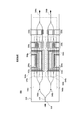
- FIG. 1 is a diagram showing a configuration of an optical modulation module according to the first embodiment of the present invention.
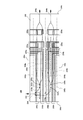
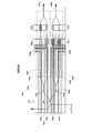
- FIG. 2 is a diagram showing a configuration of a light modulation element used in the light modulation module shown in FIG.
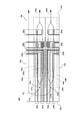
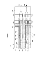
- FIG. 3 is a diagram showing a first modification of the light modulation element that can be used in the light modulator shown in FIG.
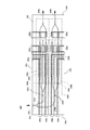
- FIG. 4 is a diagram showing a second modification of the light modulation element that can be used in the light modulator shown in FIG.
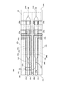
- FIG. 5 is a diagram showing a third modification of the light modulation element that can be used in the light modulator shown in FIG.
- FIG. 6 is a diagram showing a configuration of a conventional light modulation element that can be used alone.
- FIG. 7 is a diagram showing a first conventional example of a light modulation element housed in the same housing together with an electronic circuit.
- FIG. 8 is a diagram showing a second conventional example of a light modulation element housed in the same housing together with an electronic circuit.
- FIG. 1 is a diagram showing a configuration of an optical modulation module 100 according to a first embodiment of the present invention.
- the light modulation module 100 includes a housing 102, a light modulation element 104 housed in the housing 102, and an electronic circuit 106 for driving the light modulation element 104.
- the light modulation element 104 is, for example, a DP-QPSK modulator.
- the light modulation element 104 is composed of, for example, a rectangle having a pair of short sides and a pair of long sides longer than the short sides.
- a cover (not shown), which is a plate body, is fixed to the opening of the housing 102, and the inside thereof is airtightly sealed.
- the light modulation module 100 also has signal pins 110a, 110b, 110c, 110d for inputting an electric signal used for modulation of the light modulation element 104, and these signal pins 110a, 110b, 110c, 110d in the housing 102. It has a feed-through unit 108 for introduction.
- the four electrical signals for driving each of the four Machzenda modulators constituting the two nested Machzenda modulators included in the light modulation element 104 are the four signal pins 110a, 110b, 110c, It is input from 110d.
- the optical modulation module 100 includes an input optical fiber 114 for inputting light into the housing 102, and an output optical fiber 120 for guiding the light modulated by the light modulation element 104 to the outside of the housing 102.
- the input optical fiber 114 and the output optical fiber 120 are fixed to the housing 102 via the supports 122 and 124, which are fixing members, respectively.
- the light input from the input optical fiber 114 is collimated by the lens 130 arranged in the support 122, and then passed through the prism 132 and the lens 134 on the long side of one of the light modulation elements 104 (the long side on the upper side in the drawing). It is input to the light modulation element 104 from the side).
- the input optical fiber 114 is introduced into the housing 102 via the support 122, and the end portion of the introduced input optical fiber 114 is introduced. Can be performed by arranging the light modulation element 104 on the long side side of one of the light modulation elements 104.
- the light modulation module 100 also has an optical unit 116 that polarizes and synthesizes two modulated lights output from the light modulation element 104.
- the light that has been polarized and synthesized and output from the optical unit 116 is collected by the lens 118 arranged in the support 124 extending to the inside of the housing 102 and coupled to the output optical fiber 120.
- the high-frequency electric signal for driving the light modulation element 104 output from the electronic circuit 106 is a signal of the light modulation element 104 directly from the substrate of the electronic circuit 106 or indirectly via a relay board by wire bonding or the like. It is connected to one end of an electrode (described later). Further, the optical modulation module 100 includes two terminators 112a and 112b having predetermined impedances in the housing 102.
- FIG. 2 is a diagram showing an example of the configuration of the light modulation element 104 housed in the housing 102 of the light modulation module 100 shown in FIG.
- the light modulation element 104 is, for example, a waveguide type optical element that performs DP-QPSK modulation, and is composed of, for example, an optical waveguide (dotted line of thick line in the figure) formed on a substrate 230 made of LN.
- These optical waveguides can be formed by thermally diffusing Ti on the surface of the substrate 230, but are not limited thereto.
- the substrate 230 is thinned to a thickness of several microns, and the thickness of the line portion forming the optical waveguide is made thicker than the thickness of the other portion, so that the effective refractive index of the line portion is changed to another. It may be a rib-type optical waveguide formed higher than the portion.
- the substrate 230 is, for example, rectangular, and has two short sides 260a and 260b extending in the vertical direction and facing each other, and extending in the horizontal direction and short sides 260a orthogonal to the short sides 260a and 260b. It has two long sides 260c and 260d facing each other, which are longer than 260b.
- the short sides 260a and 260b face each other in parallel
- the long sides 260c and 260d face each other in parallel
- the short sides 260a and 260b extend in the extending direction and the long sides 260c and 260d extend in parallel.
- the light modulation element 104 has two nested Machzenda type optical waveguides 240a and 240b (each surrounded by a chain line in the figure), each of which performs a QPSK modulation operation.
- These nested Machzenda type optical waveguides 240a and 240b are two Machzenda type optical waveguides 244a (inside the rectangle shown by the broken line in the figure) 246b (inside the rectangle shown by the broken line) provided in each of the two waveguide portions forming the pair of parallel waveguides. Includes 244b (inside the dashed line rectangle) and 246b (inside the dashed line rectangle).
- the nested Machzenda type optical waveguides 240a and 240b QPSK-modulate the light input from the modulated light input terminals 242a and 242b, respectively, and QPSK-modulate the modulated light (output) to the respective output waveguides 248a and 248b. Output from.
- the four Machzenda-type optical waveguides 240a and 240b constituting the nested Machzenda-type optical waveguides 240a and 240b are parallel to each other (thus, these Machzenda-type optical waveguides 244a, 246b, 244b, and 246b).
- the waveguide) is configured to extend along one side of the substrate 230, for example, the long side 260c or 260d.
- signal electrodes 250a, 252a, 250b for causing each of the four Machzenda-type optical waveguides 244a, 246a, 244b, and 246b constituting the nested Machzenda-type optical waveguides 240a and 240b to perform modulation operations, 252b is provided.
- the signal electrodes 250a, 252a, 250b, and 252b are composed of, for example, two ground electrodes and one center electrode sandwiched between the two ground electrodes.
- the signal electrodes 250a, 252a, 250b, and 252b of the substrate 230 are different from the long side 260c or 260d, which is one side, along the direction in which the two nested Machzenda type optical waveguides 240a and 240b extend, respectively. It is formed so as to extend to another side, for example, the short side 260a.
- the signal electrodes 250a, 252a, 250b, 252b are arranged from the short side 260a on the left side of the drawing along the extending direction of the nested Machzenda type optical waveguide 240a, 240b (hence, the long side 260c). (Along the extending direction of 260d), it extends linearly to the Machzenda type optical waveguides 244a, 246a, 244b, and 246b constituting the nested Machzenda type optical waveguides 240a and 240b.
- the signal electrodes 250a, 252a, 250b, and 252b are connected to the signal output electrodes of the electronic circuit 106 at the ends arranged on the short side 260a, respectively.
- the four high-frequency electric signals input from the electronic circuit 106 on the short side 260a are transferred to the four Machzenda-type optical waveguides 244a, 246a, 244b, and 246b without changing their propagation directions. Propagate.
- leakage of the high frequency electric signal input from the electronic circuit 106 is suppressed, so that the light modulation element 104 is placed in the same housing 102 in the same housing 102 without deteriorating the high frequency characteristics. Can be accommodated with.
- the signal electrodes 250a and 252a are formed so as to extend toward the long side 260c after extending along the extending direction of the nested Machzenda type optical waveguide 240a. Then, the signal electrodes 250a and 252a are connected to the terminator 112a in the end arrangement 254a on the long side 260c. Further, the signal electrodes 250b and 252b are formed so as to extend toward the long side 260d after extending along the extending direction of the nested Machzenda type optical waveguide 240b. Then, the signal electrodes 250b and 252b are connected to the terminator 112b in the end arrangement 254b on the long side 260d. As a result, each of the four high-frequency electric signals input from the electronic circuit 106 on the short side 260a propagates in the signal electrodes 250a, 252a, 250b, and 252b as traveling waves.
- the light modulation element 104 is further provided with bias electrodes 256a, 258a, 256b, and 258b on the substrate 230 for adjusting the operating points of the nested Machzenda type optical waveguides 240a and 240b, if necessary.
- the input light to the light modulation element 104 is input from the input optical fiber 114 connected to the long side 260c of the substrate 230.
- light is input along the extending direction of the nested Machzenda type optical waveguides 540a and 540b, such as the branched waveguide 534 in the conventional light modulation element 700 shown in FIG. Does not have a branched waveguide.
- the light modulation element 104 includes a branched waveguide 234 arranged so that light is input from a certain direction of the long side 260c, which is one side of the substrate 230. Further, the branched waveguide 234 is formed so as to be line-symmetrical with respect to the propagation direction of the light input to the branched waveguide 234 and to output the two branched lights in a direction different from the propagation direction. It is composed of a Y-branched optical waveguide.
- the branched waveguide 234 is arranged so that the propagation direction of the light input to the branched waveguide 234 from a certain direction of the long side 260c is along the short side 260a. There is.
- the two branch outputs output from the branch waveguide 234 are guided and connected to the modulated optical input terminals 242a and 242b of the nested Machzenda type optical waveguides 240a and 240b by the connection waveguides 270a and 270b, respectively. ..
- the branched waveguide 234 has, for example, two branches when exiting the portion formed in line symmetry (the portion surrounded by the rectangular broken line indicating the branched waveguide 234 in FIG. 2).
- the distance W1 of the output light is formed to be smaller than the distance W2 of the modulated light input ends 242a and 242b, which are the light input ends of the two nested Machzenda type optical waveguides 240a and 240b (that is, W1 ⁇ W2). ..
- the modulated optical input ends 242a and 242b are used as the positions of the branch points 280a and 280b of the two branched waveguides constituting the respective input portions of the nested Machzenda type optical waveguides 240a and 240b. It can also be defined. In this case, the interval W2 is defined as the distance between the two bifurcation points 280a and 280b.
- the connecting waveguides 270a and 270b are composed of a linear waveguide and a curved waveguide as shown in FIG.
- the connection waveguides 270a and 270b have a total propagation loss from the light inflow portion of the branch waveguide 234 to the modulated light input ends 242a and 242b of the two nested Machzenda type optical waveguides 240a and 240b, respectively. , Are configured to be equal to each other. As a result, for example, even if the branch ratio of the branch waveguide 234 has a deviation from 1: 1 in design, the deviation is corrected by the bending loss in the bending waveguide portion of the connecting waveguides 270a and 270b. This will improve the degree of freedom in design.
- the light modulation element 104 having the above configuration is a branch guide in which light is input along the extending direction of the nested Machzenda type optical waveguides 240a and 240b as in the branch waveguide 534 in FIG. Since no waveguide is used, it is not necessary to use the L-shaped input waveguide 632 shown in FIG. 7, and the size increases in the left-right direction shown in FIG. 7 (the length indicated by “a” in the figure increases). ) Does not occur.
- the Y-branch waveguide constituting the branch waveguide 234 has two branched lights branched with respect to the propagation direction of the input light. Even if they are formed so as to be output in different directions, they can be easily configured so that the input light is accurately and evenly distributed (that is, a 1: 1 branching ratio can be easily realized). .. Therefore, the amount of light input to the two nested Machzender type optical waveguides 240a and 240b can be made the same, and the occurrence of distortion in the modulated waveform can be easily suppressed.
- the Y-branch waveguide that constitutes the branch waveguide 234 may be configured to be line-symmetrical with respect to the line segment in the propagation direction of the input light in order to secure a branch ratio of 1: 1 as described above. It is not always necessary to output one branch output light in the same direction as the above input light. Therefore, in the branched waveguide 234, as long as the above-mentioned line-symmetrical shape is maintained, the emission direction of one of the branched outputs is directed toward the nested Machzenda type optical waveguide 240a closer to the branched waveguide 234. Can be designed to.
- connection waveguide 270a leading to the modulation light input end 242a of the closer nested Machzenda type optical waveguide 240a while having a larger radius of curvature and shorter. It becomes.
- the exit direction of the other branch output is from the symmetry of the branch point of the branch waveguide 234 to the direction away from the distant nested Machzenda type optical waveguide 240b.
- the connecting waveguide 270b leading to the modulated optical input end 242b of the distant nested Machzenda type optical waveguide 240b can be configured to be longer than the connecting waveguide 270a, the bending loss of the optical waveguide is restricted (that is, that is). It can be designed freely and easily within the range of radius of curvature).
- the branch output light output from the branch waveguide 234 is connected to the modulated light input terminals 242a and 242b of the nested Machzenda type optical waveguides 240a and 240b by the connection waveguides 270a and 270b as described above. Therefore, for example, when it is desired to widen the distance W2 between the nested Machzenda type optical waveguides 240a and 240b for improving crosstalk, it is only necessary to adjust the extension distance of the connecting waveguides 270a and 270b along the short side 260a. It is not necessary to widen the interval W1 of the branch output light in the branch waveguide 234. Therefore, in the light modulation element 104, unlike the conventional light modulation element 700 shown in FIG.
- the light modulation element 104 does not cause deterioration of high frequency characteristics and light modulation characteristics, and does not cause an increase in its own size (thus, without causing an increase in the size of the housing 102), and is the same housing. It may be housed in 102 with the electronic circuit 106.
- FIG. 3 is a diagram showing a configuration of the light modulation element 304 according to the first modification.
- the same components as the light modulation element 104 shown in FIG. 2 shall be shown using the same reference numerals as those in FIG. 2, and the above description of FIG. 2 shall be incorporated.
- the light modulation element 304 shown in FIG. 3 has the same configuration as the light modulation element 104, except that it has an input waveguide 332 instead of the input waveguide 232.
- the input waveguide 232 in the light modulation element 104 guides the input light input from the long side 260c to the branch waveguide 234 without changing its propagation direction, whereas the input of the light modulation element 304 of this modification is
- the waveguide 332 propagates the input light input from the short side 260b along the long side 260c, changes the propagation direction by 90 degrees, and connects to the branch waveguide 234. That is, while receiving the input light from the short side 260b, the branch waveguide 234 is configured so that the light is input from a certain direction of the long side 260c.
- the input optical fiber 114 is inserted inside the housing 102. There is no need to bend 90 degrees towards the long side 260c. Therefore, when the light modulation element 304 is used, a space for routing the input optical fiber 114 in the housing 102 becomes unnecessary. For example, by changing the shape of the electronic circuit 106 while maintaining the area, the shape of the electronic circuit 106 can be changed. The size of the housing 102 in the width direction (vertical direction in the drawing) can be further reduced.
- FIG. 4 is a diagram showing a configuration of the light modulation element 404 according to the second modification.
- the same components as the light modulation element 104 shown in FIG. 2 are shown using the same reference numerals as those in FIG. 2, and the above description of FIG. 2 is incorporated.
- the light modulation element 404 shown in FIG. 4 has the same configuration as the light modulation element 104, except that it has a connection waveguide 270a'instead of the connection waveguide 270a.
- the connecting waveguide 270a' has the same configuration as that of the connecting waveguide 270a, but after the light output from the branch waveguide 234 is once propagated in the same direction as the input light of the branch waveguide 234. , The point of leading to the modulated light input end 242a is different.
- the configuration in which the connecting waveguide 270a is formed toward the modulated optical input end 242a of the Machzenda type optical waveguide 240a immediately after the branch at the branch waveguide 234 is different as shown in FIGS. 2 and 3.
- the waveguide after branching can be connected to a plurality of Machzenda type optical waveguides 240a and 240b while suppressing the size of the substrate 230 in the length direction (horizontal direction in the drawing).
- the degree of freedom in arranging the Machzenda type optical waveguides 240a and 240b can be increased.
- FIG. 5 is a diagram showing a configuration of the light modulation element 504 according to the third modification.
- the same components as the light modulation element 104 shown in FIG. 2 are shown using the same reference numerals as those in FIG. 2, and the above description of FIG. 2 is incorporated.
- the light modulation element 504 shown in FIG. 5 has the same configuration as the light modulation element 104, except that the connection waveguide 470a is provided instead of the connection waveguide 270a.
- the connecting waveguide 470a has the same configuration as the connecting waveguide 270a, except that a meandering portion 472 is included in the middle of the connecting waveguide 470a.
- the connecting waveguides 470a and 270b are optical paths from the light inflow portion of the branch waveguide 234 to the modulated optical input ends 242a and 242b, which are the optical input ends of the two nested Machzenda type optical waveguides 240a and 240b.
- the lengths are configured to be the same as each other.
- the light modulation element 504 having the above configuration is configured so that the optical path lengths from the end of the long side 260c of the input waveguide 232 to the modulated optical input ends 242a and 242b are equal to each other.
- the present invention is not limited to the configuration of the above-described embodiment and its modifications, and can be implemented in various embodiments without departing from the gist thereof.
- the substrate 230 has, for example, two short sides 260a and 260b facing each other in parallel and two long sides 260c and 260d facing each other in parallel, and the short sides 260a and 260b extend. It is assumed that the current direction and the extending direction of the long sides 260c and 260d are orthogonal to each other, but the present invention is not limited to this. Further, the nested Machzenda type optical waveguides 240a and 240b extend along one side, the long side 260c or 260d, and the branch waveguide 234 extends along the extending direction of the other side, the short side 260a. Therefore, the light is arranged so as to flow in from a certain direction of the long side 260c, but the present invention is not limited to this.
- the short sides 260a and 260b of the substrate 230 do not have to be parallel to each other, and the long sides 260c and 260d may not be parallel to each other.
- the nested Machzenda-type optical waveguides 240a, 240b which are two Machzenda-type optical waveguides connected to the branch waveguide 234, at least each parallel waveguide extends along one side of such a substrate 230.
- the branched waveguide 234 may be arranged so that light is input from a certain direction of the one side.
- the light modulation elements 104, 304, and 404 are provided with two nested Machzenda type optical waveguides 240a and 240b, each of which performs QPSK modulation, and perform DP-QPSK modulation.
- the nested Machzenda type optical waveguides 240a and 240b two Machzenda type optical waveguides that perform normal amplitude modulation are provided, and after receiving light from one light source by the input waveguide 232, each is different. It can also be modulated by a high frequency electrical signal and output to two output optical fibers.
- the high frequency characteristics and the light modulation characteristics are not deteriorated, and the light modulation element itself.
- the light modulation element and the electronic circuit can be housed together in the same housing without increasing the size of the housing (and thus without increasing the size of the housing).
- the ground electrodes constituting the signal electrodes 250a, 252a, 250b, and 252b are provided separately from each other, but the present invention is not limited to this.
- the two adjacent ground electrodes of the adjacent signal electrodes may be formed as one continuous ground electrode by forming a conductor between them. it can.
- the ground electrode on the lower side of the signal electrode 250a is integrated with the ground electrode on the upper side of the signal electrode 252a by extending to the lower side in the drawing to form one ground electrode. can do.
- ground electrode on the lower side of the signal electrode 252a and the ground electrode on the upper side of the signal electrode 252b and the ground electrode on the lower side of the signal electrode 252b and the ground electrode on the upper side of the signal electrode 250b.
- the light modulation elements 104, 304, 404, 504 shown in the present embodiment include the nested Machzenda type optical waveguides 240a and 240b, which are two Machzenda type optical waveguides provided on the substrate 230. It has a branch waveguide 234 that branches the input light input from the outside of the substrate 230 into two.
- the light modulation elements 104, 304, 404, 504 also have two connecting waveguides 270a and 270b that guide the light branched by the branch waveguide 234 to the two nested Machzenda type optical waveguides 240a and 240b, respectively.
- each of the optical waveguides constituting the two nested Machzenda type optical waveguides 240a and 240b is configured to extend to the long side 260c, which is one side of the substrate 230.
- the branch waveguide 234 is arranged so that light is input from a certain direction of the long side 260c, which is one side, (for example, along the extending direction of the short side 260a).
- the branched waveguide 234 is formed so as to be line-symmetrical with respect to the propagation direction of the light input to the branched waveguide 234 and to output the two branched lights in a direction different from the propagation direction. ing.
- the branched waveguide 234 is arranged so that light is input from a direction having one side (long side 260c) along the direction in which the nested Machzenda type optical waveguides 240a and 240b extend. .. Therefore, even when the signal electrodes 250a, 252a, 250b, and 252b are extended along the extending direction, the directions in which the ends of these signal electrodes 250a, 252a, 250b, and 252b are located with respect to the substrate 230. Light can be incident from a different direction from the above.
- the signal electrodes 250a, 252a, 250b, 252b are used as high-frequency electric signals while avoiding competition between the incident position of light on the substrate 230 and the input position of the high-frequency electric signal. It can be formed linearly from the input position of the Nested Machzenda type optical waveguide 240a and 240b along the extending direction, and good high frequency characteristics can be obtained.
- the branch waveguide 234 in the branch waveguide 234, light is emitted from a direction having one side (long side 260c) along the direction in which the two nested Machzenda type optical waveguides 240a and 240b extend. Since they are arranged so as to be input, unlike the configuration described in Patent Document 1, even when the distance between the two nested Machzenda type optical waveguides 240a and 240b is widened, it is necessary to widen the substrate 230 in the extending direction. Absent. Therefore, good optical characteristics can be obtained by reducing crosstalk between the two nested Machzenda type optical waveguides 240a and 240b without increasing the size of the substrate 230.
- the branched waveguide 234 is formed so as to be symmetrical with respect to the propagation direction of the input light and to output the two branched lights in a direction different from the propagation direction. Therefore, it is not necessary to significantly change the light propagation direction (for example, up to 90 degrees) from the branched waveguide 234 toward the nested Machzenda type optical waveguide 240a closer to the branched waveguide 234. Therefore, in the light modulation elements 104 and 404, as compared with the configuration of Patent Document 2 using the MMI coupler that outputs the branched light in the same direction as the input light, the branched waveguide 234 is changed to the nested Machzenda type optical waveguide 240a.
- the curved waveguide of the connecting waveguide 270a to reach can be reduced in size, and thus the size of the substrate 230 can be reduced.
- the branch waveguide 234 is composed of a Y-branch optical waveguide formed line-symmetrically with respect to the propagation direction of the light input to the branch waveguide 234. According to this configuration, for example, a line-symmetrical branch waveguide 234 that can accurately realize a 1: 1 branch ratio can be easily formed.
- the distance W1 between the two branched output lights when exiting the portion formed in line symmetry is two nested Machzenda type optical waveguides. It is formed to be smaller than the distance W2 between the light input ends of 240a and 240b, respectively.
- the light modulation elements 104, 304, 404, and 504 can be compactly configured while effectively reducing the crosstalk between the two nested Machzenda type optical waveguides 240a and 240b.
- the distance between the two branched output lights is allowed to an extent (more than twice the light intensity distribution of the light wave propagating in the branched waveguide). Up to this point, it is necessary to maintain the symmetry of the branch waveguide 234. Therefore, it is more desirable that the distance W1 between the two branched output lights satisfies the above condition.
- the signal electrodes 250a, 252a, 250b, 252b are formed on the substrate 230 along the direction in which the two nested Machzenda type optical waveguides 240a, 240b extend, respectively. It is formed so as to extend to another side (for example, short side 260a) different from one side (for example, long side 260c).
- the high-frequency electric signal input from the other side is transmitted to the positions of the two nested Machzenda type optical waveguides 240a and 240b by the signal electrodes 250a, 252a, 250b and 252b.
- the two nested Machzenda type optical waveguides 240a and 240b can be linearly guided along the extending direction. Therefore, the light modulation elements 104, 304, 404, and 504 can realize good high frequency characteristics.
- the two nested Machzenda type optical waveguides 240a and 240b are the two parallel waveguides constituting the nested Machzenda type optical waveguides 240a and 240b, respectively. Includes other Machzenda light waveguides 244a, 246a and 244b, 246b.
- the DP-QPSK modulator can be compactly configured on the substrate 230.
- the two connecting waveguides 270a and 270b are both composed of a linear waveguide and a curved waveguide, and two nested Machzenda types are formed from the light inflow portion of the branched waveguide 234.
- the total propagation losses up to the modulated light input terminals 242a and 242b of the optical waveguides 240a and 240b are configured to be equal to each other.
- the linear waveguide and the curved waveguide constituting the connecting waveguides 270a and 270b are respectively such that the amounts of light input to the two nested Machzenda type optical waveguides 240a and 240b are equal. Propagation loss or bending loss can be adjusted, and the degree of freedom in design is improved.
- the two connecting waveguides 470a and 270b extend from the light inflow portion of the branch waveguide 234 to the modulated optical input ends 242a and 242b of the two nested Machzenda type optical waveguides 240a and 240b.
- the optical path lengths are configured to be the same as each other.
- the phases of the light input to the two nested Machzenda type optical waveguides 240a and 240b can be accurately matched.
- the substrate 230 has two opposing short sides 260a and 260b and two opposing long sides 260c and 260d longer than the short sides 260a and 260b. It consists of a rectangle. Further, the one side is any of the long sides 260c and 260d, and the propagation direction of light when input to the branch waveguide 234 is the direction along the short sides 260a and 260b.
- signal electrodes 250a, 250b, 252a, 252b are extended along the long side 260c, and a high-frequency electric signal is input from an end extending to the short side 260a.
- the position where the light from the outside is incident on the substrate 230 can be arranged on a side other than the short side 260a (for example, the long side 260c or the short side 260b).
- the signal electrodes 250a, 250b, 252a, and 252b are linearly extended to the two nested Machzenda type optical waveguides 240a and 240b while avoiding the conflict between the input position of the high frequency electric signal and the optical input position. It can be easily realized.
- the light modulation module 100 shown in the above embodiment includes a light modulation element of any of the light modulation elements 104, 304, 404, and 504, an electronic circuit 106 for driving the light modulation element, and the light modulation element and electrons. It has a housing 102 that houses the circuit 106.
- the optical modulation module 100 having good high frequency characteristics and optical modulation characteristics can be compactly configured.
- Optical modulation module 102 ... Housing, 104, 304, 404, 504, 600, 700, 800 ...
- Optical modulation element 106 ... Electronic circuit, 108 ... Feed-through unit, 110a, 110b, 110c, 110d ... Signal pin, 112a, 112b ... Terminator, 114 ... Input optical fiber, 116 ... Optical unit, 118 ... Lens, 120 ... Output optical fiber, 122, 124 ... Support, 230, 530 ... Substrate, 232, 332, 532, 632, 732 ... Input waveguides, 234, 534 ... Branch waveguides, 240a, 240b, 540a, 540b ...
- Nested Machzenda type optical fiber waveguides 242a, 242b, 542a, 542b ... Modulated light input terminals, 244a, 244b, 246a, 246b, 544a, 544b, 546a, 546b ... Machzenda type optical fiber, 248a, 248b, 548a, 548b ... Output waveguide, 250a, 250b, 252a, 252b, 550a, 550b, 552a, 552b, 650a, 650b, 652a, 652b, 750a, 750b. , 752a, 752b ... Signal electrodes, 254a, 254b, 554a, 554b ...
Landscapes
- Physics & Mathematics (AREA)
- Nonlinear Science (AREA)
- General Physics & Mathematics (AREA)
- Optics & Photonics (AREA)
- Engineering & Computer Science (AREA)
- Microelectronics & Electronic Packaging (AREA)
- Chemical & Material Sciences (AREA)
- Ceramic Engineering (AREA)
- Crystallography & Structural Chemistry (AREA)
- Optical Modulation, Optical Deflection, Nonlinear Optics, Optical Demodulation, Optical Logic Elements (AREA)
- Optical Integrated Circuits (AREA)
Abstract
高周波特性及び光変調特性の劣化を招くことなく、かつ筺体サイズの増大を招くことなく、同一筺体内に電子回路と共に収容し得る光変調素子が実現される。 基板に設けられた2つのマッハツェンダ型光導波路と、基板の外部から入力される入力光を2つに分岐する分岐導波路と、分岐導波路により分岐された光を2つのマッハツェンダ型光導波路へそれぞれ導く2つの接続導波路と、2つのマッハツェンダ型光導波路を構成する光導波路を伝搬する光波をそれぞれ制御する電極と、により構成され、2つのマッハツェンダ型光導波路のそれぞれの並行導波路は、基板の一の辺に沿って延在するよう構成されており、分岐導波路は、上記一の辺のある方向から光が入力されるよう配され、当該分岐導波路に入力される光の伝搬方向に関し線対称であって且つ分岐された2つの光が当該伝搬方向と異なる方向へ出力されるように形成されている。
Description
本発明は、光変調器及び光変調モジュールに関する。
高速/大容量光ファイバ通信システムにおいては、導波路型の光変調器を組み込んだ光送信装置が多く用いられている。中でも、電気光学効果を有するLiNbO3(以下、LNともいう)を基板に用いた光変調素子は、インジウムリン(InP)、シリコン(Si)、あるいはガリウム砒素(GaAs)などの半導体系材料を用いた変調素子に比べて、光の損失が少なく且つ広帯域な光変調特性を実現し得ることから、高速/大容量光ファイバ通信システムに広く用いられている。
一方、光ファイバ通信システムにおける変調方式は、近年の伝送容量の増大化の流れを受け、QPSK(Quadrature Phase Shift Keying)やDP-QPSK(Dual Polarization - Quadrature Phase Shift Keying)等、多値変調や、多値変調に偏波多重を取り入れた伝送フォーマットが主流となっている。
近年のインターネットサービスの普及加速は通信トラフィックのより一層の増大を招き、光通信システムについての、継続的な高速大容量化の検討が今も進められている。その一方で、装置の小型化に対する要求は不変であり、光変調素子そのものの小型化に加えて、電子回路と光変調素子とを一つの筺体に収容し、光変調モジュールとして集積化する等の取り組みも進められている。
例えば、光変調素子と当該光変調素子を駆動する高周波ドライバアンプとを一つの筺体内に集積して収容し、光入出力部を当該筺体の片側短辺に並列配置することで、小型・集積化を図った光変調モジュールが提案されている。
図6は、上記のような集積化が行われる前の、単体として用いられるDP-QPSK変調器を構成する光変調素子の、従来の構成の一例を示す図である。DP-QPSK変調器を構成する光変調素子600は、LNである基板530上に構成され、図示左方から入力された光を受ける入力導波路532と、入力された光を同じ光量を有する2つの光に分岐する分岐導波路534と、を含む。また、光変調素子600は、分岐導波路534により分岐されたそれぞれの光を変調する2つの変調部である、いわゆるネスト型マッハツェンダ型光導波路540a、540b(それぞれ、図示一点鎖線で囲まれた部分)を含む。
ネスト型マッハツェンダ型光導波路540a、540bは、それぞれ、一対の並行導波路を成す2つの導波路部分のそれぞれに設けられた2つのマッハツェンダ型光導波路544a(図示破線内部分)、546b(図示二点鎖線内部分)、および544b(図示破線内部分)、546b(図示二点鎖線内部分)を含む。これにより、ネスト型マッハツェンダ型光導波路540a、540bは、それぞれ変調光入力端542a、542bから入力された光を、それぞれQPSK変調した後、変調後の光(出力)をそれぞれの出力導波路548a、548bから図示右方へ出力する。
これら2つの出力光は、その後、基板530外に配された光学部品により偏波合成されて一つの光ビームにまとめられ、例えばレンズを介して光ファイバ端末へ入力されて、伝送路ファイバへと導かれる。
基板530上には、ネスト型マッハツェンダ型光導波路540a、540bを構成する合計4つのマッハツェンダ型光導波路544a、546a、544b、546bのそれぞれに変調動作を行わせるための信号電極550a、552a、550b、552bが設けられている。信号電極550a、552a、550b、552bは、例えば、それぞれ2つの接地電極と、当該2つの接地電極に挟まれた1つの中心電極とで構成されている。
信号電極550a、552aは、例えば、基板530の図示上側の長辺の左方及び右方に、それぞれ両端部が配列されている。また、信号電極550b、552bは、例えば、基板530の図示下側の長辺の左方及び右方に、それぞれ両端部が配列されている。信号電極550a、552a、および550b、552bは、図示右方の端部配列554aおよび554bに接続された終端抵抗(不図示)により終端される。これにより、図示左方に配列された端部から入力された高周波電気信号は、進行波となって信号電極550a、552a、550b、552b内を伝搬する。この高周波電気信号は、例えば光変調素子600に100Gb/sを超える伝送レートの変調を行わせる際には、マイクロ波領域の周波数を有する。
なお、基板530上には、必要に応じて、ネスト型マッハツェンダ型光導波路540a、540bの動作点を調整するためのバイアス電極556a、558a、556b、558bも設けられる。
上記の構成を有する従来のDP-QPSK変調器は、単体として良好に機能するものの、更なる高速化に向けて上記のような電子回路との集積化を行う場合には、いくつかの改善の余地を有する。その一つは、光の入出力部(入力導波路532、出力導波路548a、548b)が基板530の図示左右において対向する2つの短辺に設けられていることから、信号電極550a、552a、および550b、550bの端部が、これらの短辺を避けて基板530の図示上下の2つの長辺にそれぞれ設けられる点である。すなわち、配置の競合を避けるため、光の入出力部は2つの短辺に、信号電極550a等の端部は2つの長辺にそれぞれ配されている。
一般に、マイクロ波を伝搬させる信号電極は、当該信号電極を伝搬するマイクロ波エネルギの空中への漏れをできる限り防止すべく、屈曲部や曲がり部を極力含まないように構成することが望ましい。これに対し、上記従来の光変調素子600では、上記光の入出力部との配置スペースの競合を避けるべく、信号電極550a、552a、および550b、550bのそれぞれの端部を基板530のそれぞれの長辺に設ける結果、信号電極550a、552a、550b、550bのそれぞれは、マッハツェンダ型光導波路544a、546a、544b、546bのそれぞれに至るまでの間に曲がり線路(曲線線路)等により構成される屈曲部を含むこととなり得る。
このような、信号電極における屈曲部を減らす構成として、従来、図7に示す光変調素子700のように、L字型に曲がった入力導波路632を備えて、ネスト型マッハツェンダ型光導波路540a、540bの光導波路の延在方向に対し直交する方向からの光入力を受ける構成が提案されている(特許文献1)。
また、他の構成として、従来、図8に示す光変調素子800のように、図6における分岐導波路534に代えて、ネスト型マッハツェンダ型光導波路540a、540bの光導波路の延在方向に対し直交する方向に伝搬する光入力を2つの光に分岐して、2つの分岐光を当該光入力の伝搬方向と同じ方向へ出力するMMIカプラ734を備える構成が提案されている(特許文献2)。この構成では、MMIカプラ734を出たそれぞれの分岐光は、それらの伝搬方向を90度曲げるための曲がり導波路で構成される接続導波路を介して、それぞれネスト型マッハツェンダ型光導波路540a、540bへ入力される。
なお、図7、図8において、図6に示す構成要素と同じ構成要素については、図6に示す符号と同じ符号を用いて示している。
図7および図8に示す光変調素子700、700は、入力光が基板530の長辺側(それぞれ図示上側の辺)から入力されるため、信号電極650a、652a、650b、652b、及び信号電極750a、752a、750b、750bを、基板530の一の短辺(それぞれ図示左側の辺)から、ネスト型マッハツェンダ型光導波路540a、540bまで、屈曲することなく、ネスト型マッハツェンダ型光導波路540a、540bの延在方向に沿って直線状に構成することができる。このため、伝送レートの高速化に伴って高周波信号の周波数が増加しても、これらの信号電極からのマイクロ波の漏洩が回避され得る。
しかしながら、図7に一例を示した特許文献1の構成では、L字型の入力導波路632を導入したため、図示の長さaにわたり基板530が長さ方向に長くならざるを得ない。このため、上述した光変調素子の小型化への要求に反することとなる。また、分岐導波路534をそのまま用いるため、2つのネスト型マッハツェンダ型光導波路540a、540b間のクロストークを低減すべく、これらのネスト型マッハツェンダ型光導波路540a、540bの間隔を広げると、分岐導波路534からネスト型マッハツェンダ型光導波路540a、540bのそれぞれに至る接続導波路の長さが長くなって、基板530の長さは長くなる。これは、接続導波路の長さを一定にしたまま上記間隔を広げるためには、接続導波路に設ける曲がり部分の曲率半径を小さくする必要が生ずるが、曲がり損失との関係から、上記曲率半径を際限なく小さくすることはできないためである。
したがって、例えば伝送レートの増加等に起因してネスト型マッハツェンダ型光導波路540a、540bを駆動する高周波電気信号の周波数が増加したような場合に、上記間隔を広げてクロストークを低減しようとすると、基板530の長さ方向が更に拡大されることとなり、上記小型化の要請に応えることが更に困難となる。
また、図8に一例を示した特許文献2の構成では、上述のように、MMIカプラ734を出たそれぞれの分岐光は、それらの伝搬方向を90度曲げるための曲がり導波路を含んだ接続導波路を介して、それぞれネスト型マッハツェンダ型光導波路540a、540bへ入力される。このため、上記と同様に、曲がり導波路部分の曲率半径の制約から、接続導波路を形成するためには、基板部分の面積を一定以上確保する必要が生じ、基板530の小型化を図ることが困難となる。
一方、MMIカプラ734の分岐出力光を、当該MMIカプラ734の入力光の伝搬方向と異なる方向へ出力させようとすると、MMIカプラ734を構成するモード干渉部分の設計が複雑化し、所望の(例えば1:1の)分岐比を精度よく実現することが困難となり得る。
すなわち、上述した従来の光変調素子は、電子回路と共に同一の筺体内に収容する用途においては、更に改善の余地がある。
上記背景より、高周波特性及び光変調特性の劣化を招くことなく、かつ筺体サイズの増大を招くことなく、同一の筺体内に電子回路と共に収容することのできる光変調素子を実現することが望まれている。
本発明の一の態様は、基板上に設けられた2つのマッハツェンダ型光導波路と、前記基板の外部から入力される入力光を2つに分岐する分岐導波路と、前記分岐導波路により分岐された光を前記2つのマッハツェンダ型光導波路へそれぞれ導く2つの接続導波路と、前記2つのマッハツェンダ型光導波路を構成する光導波路を伝搬する光波をそれぞれ制御する電極と、により構成される光変調素子であって、前記2つのマッハツェンダ型光導波路のそれぞれの並行導波路は、前記基板の一の辺に沿って延在するよう構成されており、前記分岐導波路は、前記一の辺のある方向から光が入力されるよう配され、当該分岐導波路に入力される光の伝搬方向に関し線対称であって且つ分岐された2つの光が当該伝搬方向と異なる方向へ出力されるように形成されている。
本発明の他の態様によると、前記分岐導波路は、当該分岐導波路に入力される光の伝搬方向に関し線対称に形成されたY分岐光導波路で構成される。
本発明の他の態様によると、前記分岐導波路は、前記線対称に形成された部分を出るときの2つの分岐出力光の間隔が、前記2つのマッハツェンダ型光導波路のそれぞれの光入力端の間隔よりも小さく形成されている。
本発明の他の態様によると、前記電極は、それぞれ、前記2つのマッハツェンダ型光導波路が延在する方向に沿って前記一の辺と異なる前記基板の他の辺まで延在するよう形成されている。
本発明の他の態様によると、前記2つのマッハツェンダ型光導波路は、それぞれ、当該マッハツェンダ型光導波路を構成する2つの並行導波路のそれぞれに他のマッハツェンダ型光導波路を含むネスト型マッハツェンダ型光導波路である。
本発明の他の態様によると、前記2つの前記接続導波路は、共に直線導波路と曲がり導波路とで構成され、前記分岐導波路の光の流入部から、前記2つのマッハツェンダ型光導波路のそれぞれの光る入力端に至るまでの全伝搬損失が、互いに等しくなるように構成される。
本発明の他の態様によると、前記2つの接続導波路は、前記分岐導波路の光の流入部から前記2つのマッハツェンダ型光導波路の光入力端までのそれぞれの光路長が互いに同じとなるように構成される。
本発明の他の態様によると、前記基板は、2つの対向する短辺と、前記短辺より長い2つの対向する長辺と、を有する矩形であり、前記一の辺は前記長辺のいずれかであり、前記分岐導波路に入力される際の光の伝搬方向は前記短辺に沿った方向である。
本発明の他の態様は、上記いずれかの光変調素子と、前記光変調素子を駆動する電子回路と、前記光変調素子と前記電子回路とを収容する筺体と、を有する光変調モジュールである。
なお、この明細書には、2019年3月29日に出願された日本国特許出願・特願2019-067621号の全ての内容が含まれるものとする。
本発明の他の態様によると、前記分岐導波路は、当該分岐導波路に入力される光の伝搬方向に関し線対称に形成されたY分岐光導波路で構成される。
本発明の他の態様によると、前記分岐導波路は、前記線対称に形成された部分を出るときの2つの分岐出力光の間隔が、前記2つのマッハツェンダ型光導波路のそれぞれの光入力端の間隔よりも小さく形成されている。
本発明の他の態様によると、前記電極は、それぞれ、前記2つのマッハツェンダ型光導波路が延在する方向に沿って前記一の辺と異なる前記基板の他の辺まで延在するよう形成されている。
本発明の他の態様によると、前記2つのマッハツェンダ型光導波路は、それぞれ、当該マッハツェンダ型光導波路を構成する2つの並行導波路のそれぞれに他のマッハツェンダ型光導波路を含むネスト型マッハツェンダ型光導波路である。
本発明の他の態様によると、前記2つの前記接続導波路は、共に直線導波路と曲がり導波路とで構成され、前記分岐導波路の光の流入部から、前記2つのマッハツェンダ型光導波路のそれぞれの光る入力端に至るまでの全伝搬損失が、互いに等しくなるように構成される。
本発明の他の態様によると、前記2つの接続導波路は、前記分岐導波路の光の流入部から前記2つのマッハツェンダ型光導波路の光入力端までのそれぞれの光路長が互いに同じとなるように構成される。
本発明の他の態様によると、前記基板は、2つの対向する短辺と、前記短辺より長い2つの対向する長辺と、を有する矩形であり、前記一の辺は前記長辺のいずれかであり、前記分岐導波路に入力される際の光の伝搬方向は前記短辺に沿った方向である。
本発明の他の態様は、上記いずれかの光変調素子と、前記光変調素子を駆動する電子回路と、前記光変調素子と前記電子回路とを収容する筺体と、を有する光変調モジュールである。
なお、この明細書には、2019年3月29日に出願された日本国特許出願・特願2019-067621号の全ての内容が含まれるものとする。
本発明によれば、高周波特性及び光変調特性の劣化を招くことなく、かつ筺体サイズの増大を招くことなく、同一の筺体内に電子回路と共に収容することのできる光変調素子を実現することができる。
以下、本発明の実施形態について、図面を参照して説明する。図1は、本発明の第1の実施形態に係る光変調モジュール100の構成を示す図である。光変調モジュール100は、筺体102と、当該筺体102内に収容された光変調素子104および当該光変調素子104を駆動する電子回路106と、を有する。光変調素子104は、例えば、DP-QPSK変調器である。また、光変調素子104は、例えば、一対の短辺と、当該短辺より長い一対の長辺とを有する矩形で構成される。なお、筺体102は、最終的にはその開口部に板体であるカバー(不図示)が固定されて、その内部が気密封止される。
光変調モジュール100は、また、光変調素子104の変調に用いる電気信号を入力するための信号ピン110a、110b、110c、110dと、これらの信号ピン110a、110b、110c、110dを筺体102内に導入するためのフィードスルー部108と、を有する。本実施例では、光変調素子104が備える2つのネスト型マッハツェンダ変調器を構成する4つのマッハツェンダ変調器のそれぞれを駆動するための4つの電気信号が、上記4つの信号ピン110a、110b、110c、110dから入力される。
さらに、光変調モジュール100は、筺体102内に光を入力するための入力光ファイバ114と、光変調素子104により変調された光を筺体102の外部へ導く出力光ファイバ120と、を有する。
ここで、入力光ファイバ114及び出力光ファイバ120は、固定部材であるサポート122及び124を介して筺体102にそれぞれ固定されている。入力光ファイバ114から入力された光は、サポート122内に配されたレンズ130によりコリメートされた後、プリズム132およびレンズ134を介して光変調素子104の一の長辺側(図示上側の長辺側)から当該光変調素子104へ入力される。ただし、これは一例であって、光変調素子104への光の入力は、例えば、入力光ファイバ114を、サポート122を介して筺体102内に導入し、当該導入した入力光ファイバ114の端部を光変調素子104の一の長辺側に配置することで行うものとすることもできる。
光変調モジュール100は、また、光変調素子104から出力される2つの変調された光を偏波合成する光学ユニット116を有する。偏波合成されて光学ユニット116から出力された光は、筺体102の内部まで延在するサポート124内に配されたレンズ118により集光されて出力光ファイバ120へ結合される。
電子回路106から出力される、光変調素子104を駆動する高周波電気信号は、例えばワイヤボンディング等により、電子回路106の基板から直接に、又は中継基板を介して間接に、光変調素子104の信号電極(後述)の一端に接続される。また、光変調モジュール100は、筺体102内に所定のインピーダンスを有する2つの終端器112aおよび112bを備える。
図2は、図1に示す光変調モジュール100の筺体102内に収容される光変調素子104の構成の一例を示す図である。光変調素子104は、例えばDP-QPSK変調を行う導波路型光素子であり、例えばLNで構成される基板230上に形成された光導波路(図示太線の点線)で構成される。これらの光導波路は、基板230の表面にTiを熱拡散することにより形成されるものとすることができるが、これには限られない。これらの光導波路は、例えば基板230を数ミクロンの厚さまで薄板化し、光導波路を形成するライン部分の厚さを他の部分の厚さより厚くすることで、当該ライン部分の実効屈折率を他の部分より高くして形成されるリブ型光導波路であってもよい。
基板230は、例えば矩形であり、図示上下方向に延在して対向する2つの短辺260a、260b、および当該短辺260a、260bと直交する図示左右方向に延在し、且つ短辺260a、260bよりも長さの長い、互いに対向する2つの長辺260c、260dを有する。例えば、基板230は、短辺260a、260bが互いに平行に対向し、長辺260c、260dが互いに平行に対向し、短辺260a、260bの延在方向と長辺260c、260dの延在方向とは直交している。
光変調素子104は、それぞれがQPSK変調動作を行う2つのネスト型マッハツェンダ型光導波路240a、240b(それぞれ、図示一点鎖線で囲まれた部分)を有する。これらのネスト型マッハツェンダ型光導波路240a、240bは、それぞれ、一対の並行導波路を成す2つの導波路部分のそれぞれに設けられた2つのマッハツェンダ型光導波路244a(図示破線の矩形内)、246b(図示二点鎖線の矩形内)、および244b(図示破線の矩形内)、246b(図示二点鎖線の矩形内)を含む。これにより、ネスト型マッハツェンダ型光導波路240a、240bは、それぞれの変調光入力端242a、242bから入力された光をそれぞれQPSK変調し、変調後の光(出力)をそれぞれの出力導波路248a、248bから出力する。
本実施形態では、ネスト型マッハツェンダ型光導波路240a、240bを構成する4つのマッハツェンダ型光導波路244a、246b、244b、246b(したがって、これらのマッハツェンダ型光導波路244a、246b、244b、246bのそれぞれの並行導波路)は、基板230の一の辺である例えば長辺260c又は260dに沿って延在するよう構成されている。
基板230上には、ネスト型マッハツェンダ型光導波路240a、240bを構成する合計4つのマッハツェンダ型光導波路244a、246a、244b、246bのそれぞれに変調動作を行わせるための信号電極250a、252a、250b、252bが設けられている。信号電極250a、252a、250b、252bは、例えば、それぞれ2つの接地電極と、当該2つの接地電極に挟まれた1つの中心電極とで構成されている。
信号電極250a、252a、250b、252bは、それぞれ、2つのネスト型マッハツェンダ型光導波路240a、240bが延在する方向に沿って、上記一の辺である長辺260c又は260dと異なる、基板230の他の辺である例えば短辺260aまで延在するよう形成されている。
言い換えると、本実施形態では、信号電極250a、252a、250b、252bは、図示左方の短辺260aから、ネスト型マッハツェンダ型光導波路240a、240bの延在方向に沿って(したがって、長辺260c、260dの延在方向に沿って)、ネスト型マッハツェンダ型光導波路240a、240bを構成するマッハツェンダ型光導波路244a、246a、244b、246bまで直線的に延在する。また、信号電極250a、252a、250b、252bは、短辺260aに配された端部において電子回路106の信号出力電極とそれぞれ接続される。これにより、光変調素子104では、短辺260aにおいて電子回路106から入力された4つの高周波電気信号は、その伝搬方向を変えられることなく4つのマッハツェンダ型光導波路244a、246a、244b、246bへと伝搬される。その結果、光変調素子104では、電子回路106から入力された高周波電気信号の漏洩が抑制されるので、光変調素子104を、高周波特性の劣化を招くことなく同一の筺体102内に電子回路106と共に収容することができる。
信号電極250a、252aは、ネスト型マッハツェンダ型光導波路240aの延在方向に沿って延在した後、長辺260cへ向かって曲がるように形成されている。そして、信号電極250a、252aは、長辺260c上の端部配列254aにおいて、終端器112aに接続される。また、信号電極250b、252bは、ネスト型マッハツェンダ型光導波路240bの延在方向に沿って延在した後、長辺260dへ向かって曲がるように形成されている。そして、信号電極250b、252bは、長辺260d上の端部配列254bにおいて、終端器112bに接続される。これにより、短辺260aにおいて電子回路106から入力された4つの高周波電気信号のそれぞれは、信号電極250a、252a、250b、252b内を進行波として伝搬する。
光変調素子104には、更に、基板230上に、必要に応じてネスト型マッハツェンダ型光導波路240a、240bの動作点を調整するためのバイアス電極256a、258a、256b、258bも設けられる。
光変調素子104への入力光は、基板230の長辺260cに接続される入力光ファイバ114から入力される。
特に、本実施形態の光変調素子104では、図7に示す従来の光変調素子700における分岐導波路534のような、ネスト型マッハツェンダ型光導波路540a、540bの延在方向に沿って光が入力される分岐導波路を有さない。
その代わりに、光変調素子104では、基板230の上記一の辺である長辺260cのある方向から光が入力されるよう配された分岐導波路234を備える。また、分岐導波路234は、当該分岐導波路234に入力される光の伝搬方向に関し線対称であって且つ分岐された2つの光が当該伝搬方向と異なる方向へ出力されるように形成されたY分岐光導波路で構成されている。ここで、本実施形態では、分岐導波路234は、長辺260cのある方向から当該分岐導波路234に入力される光の伝搬方向が、短辺260aに沿った方向となるように配されている。
また、分岐導波路234から出力される2つの分岐出力は、それぞれ、接続導波路270a、270bにより、ネスト型マッハツェンダ型光導波路240a、240bの変調光入力端242a、242bへ導かれて接続される。
ここで、本実施形態では、分岐導波路234は、例えば、上記線対称に形成された部分(図2において分岐導波路234を示す矩形の破線で囲まれた部分)を出るときの2つの分岐出力光の間隔W1が、2つのネスト型マッハツェンダ型光導波路240a、240bのそれぞれの光入力端である変調光入力端242a、242bの間隔W2よりも小さく形成されている(すなわち、W1<W2)。なお、変調光入力端242a、242bは、図2に示す位置のほか、ネスト型マッハツェンダ型光導波路240a、240bのそれぞれの入力部を構成する2つの分岐導波路の分岐点280a、280bの位置として定義することもできる。この場合、間隔W2は、2つの分岐点280a、280b間の距離として定義される。
さらに、本実施形態では、接続導波路270a、270bは、図2に示すように、直線導波路と曲がり導波路とで構成されている。そして、接続導波路270a、270bは、分岐導波路234の光の流入部から、2つのネスト型マッハツェンダ型光導波路240a、240bのそれぞれの変調光入力端242a、242bに至るまでの全伝搬損失が、互いに等しくなるように構成されている。これにより、例えば、分岐導波路234の分岐比が、設計上、1:1から偏差を持つような場合でも、接続導波路270a、270bの曲がり導波路部分における曲がり損失等により上記偏差を補正することができることとなり、設計自由度が向上する。
上記の構成を有する光変調素子104は、上述のように、図6における分岐導波路534のような、ネスト型マッハツェンダ型光導波路240a、240bの延在方向に沿って光が入力される分岐導波路を用いないので、図7に示すL字型に曲がった入力導波路632を用いる必要はなく、図7におけるような図示左右方向のサイズの増加(図示において「a」で示す長さの増加)は発生しない。
また、分岐導波路234を構成するY分岐導波路は、図8に示す従来の光変調素子800におけるMMIカプラ734とは異なり、入力される光の伝搬方向に対し分岐された2つの分岐光が異なる方向へ出力されるように形成されるものとしても、入力光が精度よく等分配されるように容易に構成ことができる(すなわち、1:1の分岐比を容易に実現することができる)。このため、2つのネスト型マッハツェンダ型光導波路240a、240bに入力される光の光量を同じにして、変調波形における歪の発生を容易に抑制することができる。
さらに、分岐導波路234を構成するY分岐導波路は、1:1の分岐比を確保するべく入力光の伝搬方向の線分に対し線対称に構成されていればよく、上記のように2つの分岐出力光を必ずしも上記入力光と同じ方向に出力させる必要はない。このため、分岐導波路234では、上記線対称な形状を維持する限りにおいて、一方の分岐出力の出射方向を、当該分岐導波路234に近い方のネスト型マッハツェンダ型光導波路240aの方向へ向くように設計することできる。したがって、図8に示すMMIカプラ734のように入力される光の方向と同じ方向に分岐出力光を出力する分岐導波路を用いる場合に比べて、光の方向を90度変化させる必要がなく、また、分岐導波路234に入力されてから接続導波路270aを経て変調光入力端242aに至るまでの経路における光の伝搬方向の変化に変曲点がない(すなわち、図2の構成においては、上記経路における光の伝搬方向の変化は常に一方向(半時計回り)であって、途中で逆方向(時計回り方向)へは変化しない)。このため、光変調素子104では、上記近い方のネスト型マッハツェンダ型光導波路240aの変調光入力端242aに至る接続導波路270aを、より大きな曲率半径を有しつつもより短く形成することが可能となる。
一方、分岐導波路234のうち、他方の分岐出力の出射方向は、当該分岐導波路234の分岐点の対称性から、遠い方のネスト型マッハツェンダ型光導波路240bから遠ざかる方向へ出射されることとなる。しかしながら、当該遠い方のネスト型マッハツェンダ型光導波路240bの変調光入力端242bに至る接続導波路270bは、接続導波路270aより長く構成することができるので、光導波路の曲がり損失の制約(すなわち、曲率半径の制約)の範囲内で自由にかつ容易に設計することができる。
また、分岐導波路234から出力される分岐出力光は、上述のように接続導波路270a、270bによりネスト型マッハツェンダ型光導波路240a、240bの変調光入力端242a、242bと接続される。このため、例えばクロストーク改善のためにネスト型マッハツェンダ型光導波路240a、240bの間隔W2を広げたい場合には、接続導波路270a、270bの、短辺260aに沿った延在距離を調整するだけでよく、分岐導波路234における分岐出力光の間隔W1を広げる必要はない。したがって、光変調素子104では、図7に示す従来の光変調素子700とは異なり、ネスト型マッハツェンダ型光導波路240a、240bの間隔を広げても、基板230の長さ方向(すなわち、長辺260c、260dに沿った方向)の長さを拡大する必要はない。
以上より、光変調素子104は、高周波特性及び光変調特性の劣化を招くことなく、かつ自身のサイズの増大を招くことなく(従って、筺体102のサイズの増大を招くことなく)、同一の筺体102内に電子回路106と共に収容され得る。
次に、第1の実施形態に係る光変調モジュール100に用いることのできる、光変調素子104の変形例について説明する。
<第1の変形例>
図3は、第1の変形例に係る光変調素子304の構成を示す図である。図3において、図2に示す光変調素子104と同じ構成要素については、図2における符号と同じ符号を用いて示すものとし、上述した図2についての説明を援用する。
図3は、第1の変形例に係る光変調素子304の構成を示す図である。図3において、図2に示す光変調素子104と同じ構成要素については、図2における符号と同じ符号を用いて示すものとし、上述した図2についての説明を援用する。
図3に示す光変調素子304は、光変調素子104と同様の構成を有するが、入力導波路232に代えて、入力導波路332を有する点が異なる。光変調素子104における入力導波路232は、長辺260cから入力された入力光を、その伝搬方向を変更することなく分岐導波路234へ導くのに対し、本変形例の光変調素子304の入力導波路332は、短辺260bから入力される入力光を長辺260cに沿って伝搬させた後、その伝搬方向を90度変化させて、分岐導波路234へ接続する。すなわち、短辺260bからの入力光を受け取りつつも、分岐導波路234には、長辺260cのある方向から光が入力されるように構成されている。
上記の構成を有する光変調素子304では、これを光変調モジュール100の筺体102に収容して用いた場合には、光変調素子104を用いる場合と異なり、筺体102の内部において入力光ファイバ114を長辺260cへ向けて90度曲げる必要がない。このため、光変調素子304を用いた場合には、筺体102内における入力光ファイバ114の引き回しのためのスペースが不要となり、例えば電子回路106の面積はそのままにその形状を変更等することで、筺体102の幅方向(図示上下方向)のサイズを更に小型化することができる。
<第2の変形例>
図4は、第2の変形例に係る光変調素子404の構成を示す図である。図4において、図2に示す光変調素子104と同じ構成要素については、図2における符号と同じ符号を用いて示すものとし、上述した図2についての説明を援用する。
図4は、第2の変形例に係る光変調素子404の構成を示す図である。図4において、図2に示す光変調素子104と同じ構成要素については、図2における符号と同じ符号を用いて示すものとし、上述した図2についての説明を援用する。
図4に示す光変調素子404は、光変調素子104と同様の構成を有するが、接続導波路270aに代えて接続導波路270a´を有する点が異なる。接続導波路270a´は、接続導波路270aと同様の構成を有するが、分岐導波路234から出力された光を、一旦、分岐導波路234の入力光の伝搬方向と同じ方向へ伝搬させた後、変調光入力端242aへ導く点が異なる。
図4の構成においては、図2や図3のように分岐導波路234での分岐後すぐにマッハツェンダ型光導波路240aの変調光入力端242aへ向かって接続導波路270aが形成される構成は異なり、接続導波路270a´は、接続導波路270bの直線導波路部分に対し狭い間隔で並行に設けられた直線導波路部分を含む。これにより、図4の構成では、基板230の長さ方向(図示左右方向)の大きさを抑制しながら、分岐後の導波路を複数のマッハツェンダ型光導波路240a、240bに接続できるため、複数のマッハツェンダ型光導波路240a、240bの配置の自由度を増すことが出来る。
<第3の変形例>
図5は、第3の変形例に係る光変調素子504の構成を示す図である。図5において、図2に示す光変調素子104と同じ構成要素については、図2における符号と同じ符号を用いて示すものとし、上述した図2についての説明を援用する。
図5は、第3の変形例に係る光変調素子504の構成を示す図である。図5において、図2に示す光変調素子104と同じ構成要素については、図2における符号と同じ符号を用いて示すものとし、上述した図2についての説明を援用する。
図5に示す光変調素子504は、光変調素子104と同様の構成を有するが、接続導波路270aに代えて、接続導波路470aを備える点が異なる。接続導波路470aは、接続導波路270aと同様の構成を有するが、その途中に蛇行部472が含まれている点が異なる。これにより、接続導波路470a、270bは、分岐導波路234の光の流入部から2つのネスト型マッハツェンダ型光導波路240a、240bの光入力端である変調光入力端242a、242bまでのそれぞれの光路長が、互いに同じとなるように構成されている。
上記の構成を有する光変調素子504は、入力導波路232の長辺260cの端部からそれぞれ変調光入力端242a、242bに至るまでの光路長が互いに等しくなるように構成されることとなるので、例えば2つのネスト型マッハツェンダ型光導波路240a、240bに入力される光の位相を、変調光入力端242a、242bにおいて互いに同じにしたい場合に好適である。
なお、本発明は上記実施形態およびその変形例の構成に限られるものではなく、その要旨を逸脱しない範囲において種々の態様において実施することが可能である。
例えば、本実施形態では、基板230は、例えば互いに平行に対向する2つの短辺260a、260bと、互いに平行に対向する2つの長辺260c、260dとを有し、短辺260a、260bの延在方向と長辺260c、260dの延在方向が直交する矩形であるものとしたが、これには限られない。また、ネスト型マッハツェンダ型光導波路240a、240bは、一の辺である長辺260c又は260dに沿って延在し、分岐導波路234は、他の辺である短辺260aの延在方向に沿って、長辺260cのある方向から光が流入されるよう配されるものとしたが、これには限られない。
基板230の、短辺260a、260bは互いに平行でなくてもよく、及び又は、長辺260c、260dは互いに平行でなくてもよい。分岐導波路234に接続される2つのマッハツェンダ型光導波路であるネスト型マッハツェンダ型光導波路240a、240bは、少なくとも、それぞれの並行導波路が、そのような基板230の一の辺に沿って延在していればよく、分岐導波路234は、当該一の辺のある方向から光が入力されるように配されていればよい。
また、上述した実施形態及びその変形例では、光変調素子104、304、404は、それぞれがQPSK変調を行う2つのネスト型マッハツェンダ型光導波路240a、240bを備えてDP-QPSK変調を行うものとしたが、これには限られない。例えば、ネスト型マッハツェンダ型光導波路240a、240bに代えて、それぞれ通常の振幅変調を行う2つのマッハツェンダ型光導波路を備え、一つの光源からの光を入力導波路232により受信した後、それぞれが異なる高周波電気信号により変調を行って2つの出力光ファイバへ向けて出力されるものとすることもできる。
この場合でも、上述の光変調素子104、304、404における分岐導波路234を用いた構成と同様の構成を用いることにより、高周波特性及び光変調特性の劣化を招くことなく、かつ光変調素子自身のサイズの増大を招くことなく(従って、筺体サイズの増大を招くことなく)、同一の筺体内に光変調素子と電子回路とを共に収容することができることとなる。
また、上述した実施形態およびその変形例では、信号電極250a、252a、250b、252bをそれぞれ構成する接地電極は、互いに分離されて設けられるものとしたが、これには限られない。信号電極250a、252a、250b、252bのうち隣接する信号電極の隣接する2つの接地電極は、それらの間に導体が形成されることにより一つの連続する接地電極として形成されるものとすることができる。例えば、図2において、信号電極250aの図示下側の接地電極は、図示下側へ延在することにより信号電極252aの図示上側の接地電極と合体して一つの接地電極として構成されるものとすることができる。信号電極252aの図示下側の接地電極と信号電極252bの図示上側の接地電極、および信号電極252bの図示下側の接地電極と信号電極250bの図示上側の接地電極も同様である。
以上、説明したように、本実施形態に示す光変調素子104、304、404、504は、基板230上に設けられた2つのマッハツェンダ型光導波路であるネスト型マッハツェンダ型光導波路240a、240bと、基板230の外部から入力される入力光を2つに分岐する分岐導波路234と、を有する。光変調素子104、304、404、504は、また、分岐導波路234により分岐された光を上記2つのネスト型マッハツェンダ型光導波路240a、240bへそれぞれ導く2つの接続導波路270a、270bと、上記2つのネスト型マッハツェンダ型光導波路を構成する光導波路を伝搬する光波をそれぞれ制御する電極である信号電極250a、252a、250b、252bと、を有する。上記2つのネスト型マッハツェンダ型光導波路240a、240bを構成するそれぞれの光導波路は、基板230の一の辺である長辺260cに延在するよう構成されている。また、分岐導波路234は、上記一の辺である長辺260cのある方向から(例えば短辺260aの延在方向に沿って)光が入力されるよう配されている。そして、分岐導波路234は、当該分岐導波路234に入力される光の伝搬方向に関し線対称であって、且つ分岐された2つの光が当該伝搬方向と異なる方向へ出力されるように形成されている。
この構成によれば、分岐導波路234は、ネスト型マッハツェンダ型光導波路240a、240bが延在する方向に沿う一の辺(長辺260c)のある方向から光が入力されるように配される。このため、当該延在する方向に沿って信号電極250a、252a、250b、252bを延在させた場合でも、基板230に対し、これらの信号電極250a、252a、250b、252bの端部のある方向とは異なる方向から光を入射させることができる。したがって、光変調素子104、304、404、504では、基板230への光の入射位置と高周波電気信号の入力位置との競合を避けつつ、信号電極250a、252a、250b、252bを、高周波電気信号の入力位置から直線的に、ネスト型マッハツェンダ型光導波路240a、240bの延在方向に沿って形成でき、良好な高周波特性を得ることができる。
特に、上記の構成では、上述のように、分岐導波路234は、2つネスト型マッハツェンダ型光導波路240a、240bが延在する方向に沿う一の辺(長辺260c)のある方向から光が入力されるように配されるので、特許文献1に記載の構成とは異なり、2つのネスト型マッハツェンダ型光導波路240a、240bの間隔を広げる場合でも、基板230を上記延在方向に広げる必要がない。このため、基板230のサイズの増大を招くことなく、2つのネスト型マッハツェンダ型光導波路240a、240b間のクロストークを低減して良好な光学特性を得ることができる。
また、特に、上記構成によれば、分岐導波路234は、入力される光の伝搬方向に関し対称であって、且つ分岐された2つの光が当該伝搬方向と異なる方向へ出力されるように形成されているので、分岐導波路234から当該分岐導波路234に近い方のネスト型マッハツェンダ型光導波路240aに向かって光の伝搬方向を大きく(例えば90度まで)変える必要がない。このため、光変調素子104、404では、入力される光と同一方向に分岐光を出力するMMIカプラを用いる特許文献2の構成に比べて、分岐導波路234からネスト型マッハツェンダ型光導波路240aに至る接続導波路270aの曲がり導波路を部分のサイズを小さくすることができ、従って基板230のサイズを小さくすることができる。
そして、これらの効果の結果として、光変調素子104、404は、高周波特性及び光変調特性の劣化を招くことなく、かつ筺体102サイズの増大を招くことなく、当該筺体102内に電子回路106と共に収容される得る。
また、光変調素子104、304、404、504では、分岐導波路234は、当該分岐導波路234に入力される光の伝搬方向に関し線対称に形成されたY分岐光導波路で構成される。この構成によれば、例えば1:1の分岐比を精度良く実現し得る線対称の分岐導波路234を容易に形成することができる。
また、光変調素子104、304、404、504では、分岐導波路234は、上記線対称に形成された部分を出るときの2つの分岐出力光の間隔W1が、2つのネスト型マッハツェンダ型光導波路240a、240bのそれぞれの光入力端の間隔W2よりも小さく形成される。
この構成によれば、例えば2つのネスト型マッハツェンダ型光導波路240a、240bの間隔を広げた場合でも、基板230のサイズを拡大する必要がない。したがって、2つのネスト型マッハツェンダ型光導波路240a、240bの間のクロストークを効果的に低減しつつ、光変調素子104、304、404、504をコンパクトに構成することができる。
尚、分岐導波路234での分岐比を保つには、2つの分岐出力光の間で及ぼす影響が許容される程度に離間(分岐導波路を伝搬する光波の光強度分布の2倍以上)したところまで、分岐導波路234の対称性を保っておく必要がある。このため2つの分岐出力光の間隔W1は上記条件を満足することがより望ましい。
また、光変調素子104、304、404、504では、信号電極250a、252a、250b、252bは、それぞれ、2つのネスト型マッハツェンダ型光導波路240a、240bが延在する方向に沿って基板230の上記一の辺(例えば長辺260c)と異なる他の辺(例えば短辺260a)まで延在するよう形成されている。
この構成によれば、上記他の辺(短辺260a)から入力される高周波電気信号を、信号電極250a、252a、250b、252bにより、2つのネスト型マッハツェンダ型光導波路240a、240bの位置まで、当該2つのネスト型マッハツェンダ型光導波路240a、240bが延在する方向に沿って直線的に導くことができる。このため、光変調素子104、304、404、504では、良好な高周波特性を実現することができる。
また、光変調素子104、304、404、504では、2つのネスト型マッハツェンダ型光導波路240a、240bは、それぞれ、当該ネスト型マッハツェンダ型光導波路240a、240bをそれぞれ構成する2つの並行導波路のそれぞれに他のマッハツェンダ型光導波路244a、246aおよび244b、246bを含む。
この構成によれば、DP-QPSK変調器を、基板230上にコンパクトに構成することができる。
また、光変調素子104、304では、2つの接続導波路270a、270bは、共に直線導波路と曲がり導波路とで構成され、分岐導波路234の光の流入部から、2つのネスト型マッハツェンダ型光導波路240a、240bのそれぞれの変調光入力端242a、242bに至るまでの全伝搬損失が、互いに等しくなるように構成される。
この構成によれば、2つのネスト型マッハツェンダ型光導波路240a、240bに入力される光の量が等量となるように、接続導波路270a、270bを構成する直線導波路及び曲がり導波路のそれぞれの伝搬損失又は曲がり損失を調整することができ、設計自由度が向上する。
また、光変調素子504では、2つの接続導波路470a、270bは、分岐導波路234の光の流入部から上記2つのネスト型マッハツェンダ型光導波路240a、240bの変調光入力端242a、242bまでのそれぞれの光路長が互いに同じとなるように構成される。
この構成によれば、2つのネスト型マッハツェンダ型光導波路240a、240bに入力される光の位相を、精度よく一致させることができる。
また、光変調素子104、304、404、504では、基板230は、2つの対向する短辺260a、260bと、当該短辺260a、260bより長い2つの対向する長辺260c、260dと、を有する矩形で構成される。また、上記一の辺は長辺260c、260dのいずれかであり、分岐導波路234に入力される際の光の伝搬方向は短辺260a、260bに沿った方向である。
この構成によれば、例えば、矩形の基板230において、信号電極250a、250b、252a、252bを長辺260cに沿って延在させて短辺260aに至る端部から高周波電気信号を入力するものとし、基板230への外部からの光の入射位置を短辺260a以外の辺(例えば長辺260cや短辺260b)に配することができる。これにより、高周波電気信号の入力位置と光入力位置との競合を避けつつ信号電極250a、250b、252a、252bを2つのネスト型マッハツェンダ型光導波路240a、240bまで直線的に延在させる構成を、容易に実現することができる。
また、上記実施形態に示す光変調モジュール100は、光変調素子104、304、404、504のいずれかの光変調素子と、当該光変調素子を駆動する電子回路106と、当該光変調素子と電子回路106とを収容する筺体102と、を有する。
この構成によれば、良好な高周波特性及び光変調特性を有する光変調モジュール100をコンパクトに構成することができる。
100…光変調モジュール、102…筺体、104、304、404、504、600、700、800…光変調素子、106…電子回路、108…フィードスルー部、110a、110b、110c、110d…信号ピン、112a、112b…終端器、114…入力光ファイバ、116…光学ユニット、118…レンズ、120…出力光ファイバ、122、124…サポート、230、530…基板、232、332、532、632、732…入力導波路、234、534…分岐導波路、240a、240b、540a、540b…ネスト型マッハツェンダ型光導波路、242a、242b、542a、542b…変調光入力端、244a、244b、246a、246b、544a、544b、546a、546b…マッハツェンダ型光導波路、248a、248b、548a、548b…出力導波路、250a、250b、252a、252b、550a、550b、552a、552b、650a、650b、652a、652b、750a、750b、752a、752b…信号電極、254a、254b、554a、554b…端部配列、256a、256b、258a、258b、556a、556b、558a、558b…バイアス電極、260a、260b…短辺、260c、260d…長辺、270a、270b、470a…接続導波路、472…蛇行部、、734…MMIカプラ、280a、280b…分岐点。
Claims (9)
- 基板上に設けられた2つのマッハツェンダ型光導波路と、前記基板の外部から入力される入力光を2つに分岐する分岐導波路と、前記分岐導波路により分岐された光を前記2つのマッハツェンダ型光導波路へそれぞれ導く2つの接続導波路と、前記2つのマッハツェンダ型光導波路を構成する光導波路を伝搬する光波をそれぞれ制御する電極と、により構成される光変調素子であって、
前記2つのマッハツェンダ型光導波路のそれぞれの並行導波路は、前記基板の一の辺に沿って延在するよう構成されており、
前記分岐導波路は、
前記一の辺のある方向から光が入力されるよう配され、
当該分岐導波路に入力される光の伝搬方向に関し線対称であって且つ分岐された2つの光が当該伝搬方向と異なる方向へ出力されるように形成されている、
光変調素子。 - 前記分岐導波路は、当該分岐導波路に入力される光の伝搬方向に関し線対称に形成されたY分岐光導波路で構成される、
請求項1に記載の光変調素子。 - 前記分岐導波路は、前記線対称に形成された部分を出るときの2つの分岐出力光の間隔が、前記2つのマッハツェンダ型光導波路のそれぞれの光入力端の間隔よりも小さく形成されている、
請求項1または2に記載の光変調素子。 - 前記電極は、それぞれ、前記2つのマッハツェンダ型光導波路が延在する方向に沿って前記一の辺と異なる前記基板の他の辺まで延在するよう形成されている、
請求項1ないし3のいずれか一項に記載の光変調素子。 - 前記2つのマッハツェンダ型光導波路は、それぞれ、当該マッハツェンダ型光導波路を構成する2つの並行導波路のそれぞれに他のマッハツェンダ型光導波路を含むネスト型マッハツェンダ型光導波路である、
請求項1ないし4のいずれか一項に記載の光変調素子。 - 前記2つの接続導波路は、共に直線導波路と曲がり導波路とで構成され、前記分岐導波路の光の流入部から、前記2つのマッハツェンダ型光導波路のそれぞれの光入力端に至るまでの全伝搬損失が、互いに等しくなるように構成される、
請求項1ないし5のいずれか一項に記載の光変調素子。 - 前記2つの接続導波路は、前記分岐導波路の光の流入部から前記2つのマッハツェンダ型光導波路の光入力端までのそれぞれの光路長が互いに同じとなるように構成される、
請求項1ないし5のいずれか一項に記載の光変調素子。 - 前記基板は、2つの対向する短辺と、前記短辺より長い2つの対向する長辺と、を有する矩形であり、
前記一の辺は前記長辺のいずれかであり、
前記分岐導波路に入力される際の光の伝搬方向は前記短辺に沿った方向である、
請求項1ないし7のいずれか一項に記載の光変調素子。 - 請求項1ないし8のいずれか一項に記載の光変調素子と、
前記光変調素子を駆動する電子回路と、
前記光変調素子と前記電子回路とを収容する筺体と、
を有する光変調モジュール。
Priority Applications (2)
| Application Number | Priority Date | Filing Date | Title |
|---|---|---|---|
| CN201980094906.5A CN113646692B (zh) | 2019-03-29 | 2019-09-26 | 光调制元件以及光调制模块 |
| US17/599,726 US11892743B2 (en) | 2019-03-29 | 2019-09-26 | Optical modulation element and optical modulation module |
Applications Claiming Priority (2)
| Application Number | Priority Date | Filing Date | Title |
|---|---|---|---|
| JP2019-067621 | 2019-03-29 | ||
| JP2019067621A JP2020166160A (ja) | 2019-03-29 | 2019-03-29 | 光変調素子、及び光変調モジュール |
Publications (1)
| Publication Number | Publication Date |
|---|---|
| WO2020202607A1 true WO2020202607A1 (ja) | 2020-10-08 |
Family
ID=72668497
Family Applications (1)
| Application Number | Title | Priority Date | Filing Date |
|---|---|---|---|
| PCT/JP2019/037938 Ceased WO2020202607A1 (ja) | 2019-03-29 | 2019-09-26 | 光変調素子、及び光変調モジュール |
Country Status (4)
| Country | Link |
|---|---|
| US (1) | US11892743B2 (ja) |
| JP (1) | JP2020166160A (ja) |
| CN (1) | CN113646692B (ja) |
| WO (1) | WO2020202607A1 (ja) |
Cited By (2)
| Publication number | Priority date | Publication date | Assignee | Title |
|---|---|---|---|---|
| WO2022145342A1 (ja) * | 2020-12-28 | 2022-07-07 | 住友大阪セメント株式会社 | 光変調器とそれを用いた光送信装置 |
| CN116113872A (zh) * | 2021-03-24 | 2023-05-12 | 住友大阪水泥股份有限公司 | 光波导元件、光调制器、光调制模块及光发送装置 |
Citations (6)
| Publication number | Priority date | Publication date | Assignee | Title |
|---|---|---|---|---|
| US7266306B1 (en) * | 2003-10-03 | 2007-09-04 | Nortel Networks Limited | Method for optical carrier suppression and quadrature control |
| JP2013068909A (ja) * | 2011-09-26 | 2013-04-18 | Oki Electric Ind Co Ltd | 光素子 |
| WO2014129613A1 (ja) * | 2013-02-25 | 2014-08-28 | カナレ電気株式会社 | 光増幅器及びレーザ発振器 |
| JP2015102686A (ja) * | 2013-11-25 | 2015-06-04 | 日本電信電話株式会社 | 光変調器 |
| JP2016194537A (ja) * | 2015-03-31 | 2016-11-17 | 住友大阪セメント株式会社 | 導波路型光素子 |
| JP2018173450A (ja) * | 2017-03-31 | 2018-11-08 | 住友大阪セメント株式会社 | 導波路型光素子 |
Family Cites Families (3)
| Publication number | Priority date | Publication date | Assignee | Title |
|---|---|---|---|---|
| JP6287084B2 (ja) | 2012-11-09 | 2018-03-07 | 住友電気工業株式会社 | 光集積素子、光モジュール |
| JP6136363B2 (ja) | 2013-02-27 | 2017-05-31 | 住友電気工業株式会社 | 光変調モジュール |
| TWI660228B (zh) * | 2017-03-22 | 2019-05-21 | 日商日本電信電話股份有限公司 | IQ light modulator |
-
2019
- 2019-03-29 JP JP2019067621A patent/JP2020166160A/ja active Pending
- 2019-09-26 US US17/599,726 patent/US11892743B2/en active Active
- 2019-09-26 WO PCT/JP2019/037938 patent/WO2020202607A1/ja not_active Ceased
- 2019-09-26 CN CN201980094906.5A patent/CN113646692B/zh active Active
Patent Citations (6)
| Publication number | Priority date | Publication date | Assignee | Title |
|---|---|---|---|---|
| US7266306B1 (en) * | 2003-10-03 | 2007-09-04 | Nortel Networks Limited | Method for optical carrier suppression and quadrature control |
| JP2013068909A (ja) * | 2011-09-26 | 2013-04-18 | Oki Electric Ind Co Ltd | 光素子 |
| WO2014129613A1 (ja) * | 2013-02-25 | 2014-08-28 | カナレ電気株式会社 | 光増幅器及びレーザ発振器 |
| JP2015102686A (ja) * | 2013-11-25 | 2015-06-04 | 日本電信電話株式会社 | 光変調器 |
| JP2016194537A (ja) * | 2015-03-31 | 2016-11-17 | 住友大阪セメント株式会社 | 導波路型光素子 |
| JP2018173450A (ja) * | 2017-03-31 | 2018-11-08 | 住友大阪セメント株式会社 | 導波路型光素子 |
Cited By (5)
| Publication number | Priority date | Publication date | Assignee | Title |
|---|---|---|---|---|
| WO2022145342A1 (ja) * | 2020-12-28 | 2022-07-07 | 住友大阪セメント株式会社 | 光変調器とそれを用いた光送信装置 |
| JP2022104096A (ja) * | 2020-12-28 | 2022-07-08 | 住友大阪セメント株式会社 | 光変調器とそれを用いた光送信装置 |
| JP7567471B2 (ja) | 2020-12-28 | 2024-10-16 | 住友大阪セメント株式会社 | 光変調器とそれを用いた光送信装置 |
| US12474619B2 (en) | 2020-12-28 | 2025-11-18 | Sumitomo Osaka Cement Co., Ltd. | Optical modulator and optical transmission device using same |
| CN116113872A (zh) * | 2021-03-24 | 2023-05-12 | 住友大阪水泥股份有限公司 | 光波导元件、光调制器、光调制模块及光发送装置 |
Also Published As
| Publication number | Publication date |
|---|---|
| US20220197103A1 (en) | 2022-06-23 |
| US11892743B2 (en) | 2024-02-06 |
| JP2020166160A (ja) | 2020-10-08 |
| CN113646692A (zh) | 2021-11-12 |
| CN113646692B (zh) | 2024-07-16 |
Similar Documents
| Publication | Publication Date | Title |
|---|---|---|
| US9817294B2 (en) | Optical modulation device | |
| US8078015B2 (en) | Optical modulator | |
| JP3800594B2 (ja) | 光変調器 | |
| CN217386039U (zh) | 光波导元件、光调制器、光调制模块及光发送装置 | |
| CA3125932C (en) | Semiconductor mach-zehnder optical modulator | |
| JP2021162641A (ja) | 光制御素子とそれを用いた光変調デバイス並びに光送信装置 | |
| CN112859386B (zh) | 光波导元件、光调制器、光调制模块及光发送装置 | |
| CN113646692B (zh) | 光调制元件以及光调制模块 | |
| CA3154351C (en) | IQ OPTICAL MODULATOR | |
| JP2023034414A (ja) | 光導波路素子、光変調器、光変調モジュール、及び光送信装置 | |
| JP2020020890A (ja) | 光変調器 | |
| CN113534507B (zh) | 光调制器 | |
| CN117043667A (zh) | 光波导元件、光调制器、光调制模块以及光发送装置 | |
| US12498612B2 (en) | Optical modulator and optical transmission apparatus | |
| JPH04243217A (ja) | 光変調器 | |
| JP2020057024A (ja) | 光変調器 |
Legal Events
| Date | Code | Title | Description |
|---|---|---|---|
| 121 | Ep: the epo has been informed by wipo that ep was designated in this application |
Ref document number: 19923288 Country of ref document: EP Kind code of ref document: A1 |
|
| NENP | Non-entry into the national phase |
Ref country code: DE |
|
| 122 | Ep: pct application non-entry in european phase |
Ref document number: 19923288 Country of ref document: EP Kind code of ref document: A1 |