WO2020196247A1 - 光レセプタクルおよび光モジュール - Google Patents
光レセプタクルおよび光モジュール Download PDFInfo
- Publication number
- WO2020196247A1 WO2020196247A1 PCT/JP2020/012267 JP2020012267W WO2020196247A1 WO 2020196247 A1 WO2020196247 A1 WO 2020196247A1 JP 2020012267 W JP2020012267 W JP 2020012267W WO 2020196247 A1 WO2020196247 A1 WO 2020196247A1
- Authority
- WO
- WIPO (PCT)
- Prior art keywords
- optical
- light
- divided
- emitting element
- incident
- Prior art date
- Legal status (The legal status is an assumption and is not a legal conclusion. Google has not performed a legal analysis and makes no representation as to the accuracy of the status listed.)
- Ceased
Links
Images


Classifications
-
- G—PHYSICS
- G02—OPTICS
- G02B—OPTICAL ELEMENTS, SYSTEMS OR APPARATUS
- G02B6/00—Light guides; Structural details of arrangements comprising light guides and other optical elements, e.g. couplings
- G02B6/24—Coupling light guides
- G02B6/42—Coupling light guides with opto-electronic elements
-
- H—ELECTRICITY
- H10—SEMICONDUCTOR DEVICES; ELECTRIC SOLID-STATE DEVICES NOT OTHERWISE PROVIDED FOR
- H10F—INORGANIC SEMICONDUCTOR DEVICES SENSITIVE TO INFRARED RADIATION, LIGHT, ELECTROMAGNETIC RADIATION OF SHORTER WAVELENGTH OR CORPUSCULAR RADIATION
- H10F77/00—Constructional details of devices covered by this subclass
-
- H—ELECTRICITY
- H10—SEMICONDUCTOR DEVICES; ELECTRIC SOLID-STATE DEVICES NOT OTHERWISE PROVIDED FOR
- H10F—INORGANIC SEMICONDUCTOR DEVICES SENSITIVE TO INFRARED RADIATION, LIGHT, ELECTROMAGNETIC RADIATION OF SHORTER WAVELENGTH OR CORPUSCULAR RADIATION
- H10F77/00—Constructional details of devices covered by this subclass
- H10F77/40—Optical elements or arrangements
Definitions
- the present invention relates to an optical receptacle and an optical module having the same.
- an optical module having a light emitting element for transmission or a light receiving element for reception is used.
- the optical module has an optical receptacle that optically couples a light emitting element or a light receiving element with an end face of an optical fiber.
- the optical receptacle incidents light including communication information emitted from the light emitting element (hereinafter referred to as “signal light”) on the end face of the optical fiber.
- the optical receptacle guides the signal light emitted from the end face of the optical fiber to the light receiving element.
- An optical receptacle that collectively couples a plurality of light emitting elements or light receiving elements and end faces of a plurality of optical fibers has a plurality of lens surfaces arranged at a predetermined pitch, and is therefore sometimes referred to as a lens array.
- Patent Document 1 discloses an optical communication module including a monitor unit (light receiving element) that monitors a part of the emitted light emitted from a surface emitting laser.
- FIG. 1 shows an example of an optical communication module disclosed in Patent Document 1.
- the laser beam emitted from the surface emitting laser 10 and incident on the optical coupling member 32 by the first lens unit 50 is reflected by the reflecting unit 62 toward the optical fiber 21.
- the surface emitting laser 10 and the optical fiber 21 are coupled.
- the laser light emitted from the surface emitting laser 10 and incident on the optical coupling member 32 by the first lens unit 50 is transmitted by the transmitting surface 71, and the monitoring unit 40 The output is monitored by making it incident on (light receiving element).
- the optical communication module disclosed in Patent Document 1 only the output of the peripheral portion of the luminous flux (light transmitted through the transmission surface 71) can be monitored among the laser light emitted from the surface emitting laser 10. Therefore, it is not possible to monitor the overall output of the luminous flux of the surface emitting laser 10. Therefore, the optical communication module disclosed in Patent Document 1 may not be able to properly monitor the output from the surface emitting laser 10.
- the present invention has been made in view of the above circumstances, and an optical receptacle and an optical module capable of more appropriately monitoring the output from a light emitting element by monitoring the entire light emitted from the light emitting element.
- the purpose is to provide.
- the optical receptacle according to the present invention When the optical receptacle according to the present invention is arranged between a light emitting element and a photoelectric conversion device having a light receiving element for monitoring light emitted from the light emitting element and an optical transmitter, the optical receptacle and the light emitting element are used.
- the monitor light directed toward the element and the signal light directed toward the end face of the optical transmitter are separated, the monitor light is focused and transmitted toward the light receiving element, and the signal light is directed toward the end face of the optical transmitter.
- the optical separation unit has a light separation unit for reflecting the light, and a second optical surface for emitting the signal light reflected by the light separation unit toward the end face of the optical transmitter.
- the optical separation unit has the first optical.
- a plurality of divided condensing surfaces for transmitting light incident on the surface while condensing it toward the light receiving element, and light incident on the first optical surface formed in a region different from the divided condensing surface is the first. It has a plurality of divided reflecting surfaces that reflect toward two optical surfaces, and the divided reflecting surface is an inclined surface with respect to an optical axis of light incident on the first optical surface, and the divided condensing surface and the divided condensing surface.
- the split-reflecting surfaces are alternately arranged in the inclined direction of the split-reflecting surface in the central virtual cross section of the optical receptacle including the optical axis of the light incident on the first optical surface and the optical axis of the signal light.
- the optical module according to the present invention includes a light emitting element, a photoelectric conversion device having a light receiving element for monitoring the light emitted from the light emitting element, and an optical receptacle according to the present invention.
- an optical receptacle and an optical module capable of more appropriately monitoring the output from the light emitting element by monitoring the entire light emitted from the light emitting element.
- FIG. 1 is a diagram showing a conventional optical communication module.
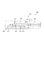
- FIG. 2 is a cross-sectional view (optical path diagram) of the optical module according to the first embodiment.
- 3A to 3C are views showing the configuration of the optical receptacle according to the first embodiment.
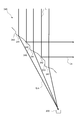
- FIG. 4 is a partially enlarged view showing the configuration of the optical separation unit and the optical path.
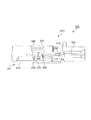
- FIG. 5 is a cross-sectional view (optical path diagram) of the optical module according to the second embodiment.
- FIG. 2 is a cross-sectional view (optical path diagram) of the optical module 100 according to the first embodiment of the present invention.
- hatching to the cross section of the optical receptacle 300 is omitted in order to show the optical path in the optical receptacle 300.
- the optical receptacle 300 will be described with the surface on the optical transmitter 400 side as the "front surface” and the surface on the photoelectric conversion device 200 side as the "bottom surface”.
- the optical module 100 has a photoelectric conversion device 200 for transmission having a light emitting element 220 and an optical receptacle 300 arranged on the photoelectric conversion device 200.
- the optical transmitter 400 is connected to the front surface of the optical receptacle 300 (the surface located on the right side in FIG. 2). That is, the optical receptacle 300 is arranged between the photoelectric conversion device 200 and the optical transmitter 400.
- the optical receptacle 300 optically couples the light emitting element 220 of the photoelectric conversion device 200 and the end face 410 of the optical transmitter 400.
- the photoelectric conversion device 200 for transmission has a light emitting element 220 and a light receiving element 230 on a substrate 210.
- the light emitting element 220 is arranged on the substrate 210 and emits light L in the direction perpendicular to the substrate surface.
- the light emitting element 220 is, for example, a vertical cavity surface emitting laser (VCSEL).
- the light receiving element 230 receives the monitor light Lm for monitoring the output of the light emitting element 220.
- the light receiving element 230 is arranged on the substrate 210 at a position farther from the optical transmitter 400 than the light emitting element 220 so as to be aligned with the light emitting element 220.
- the light receiving element 230 is, for example, a photodetector.
- the optical receptacle 300 is arranged on the substrate 210 so that the first optical surface 310 (described later) and the light emitting element 220 face each other, and the optical separation unit 340 (described later) and the light receiving element 230 face each other.
- the optical receptacle 300 By arranging the optical receptacle 300 in this way, the light emitting element 220 and the end face 410 of the optical transmitter 400 are optically coupled, and the monitor light Lm separated by the optical separation unit 340 is focused on the light receiving element 230. The output of the light emitting element 220 is monitored.
- An optical transmitter 400 corresponding to the light emitting element 220 is connected to the optical receptacle 300.
- a ferrule (not shown) or the like is attached to the end of the optical transmitter 400, and by inserting this ferrule into the recess on the front side of the optical receptacle 300, the ferrule can be combined with the second optical surface 350 of the optical receptacle 300.
- the end face 410 of the optical transmitter 400 is positioned at the opposite position.
- the optical transmitter 400 is, for example, an optical waveguide or an optical fiber.
- the optical fiber may be of a single mode system or a multi-mode system.
- the light L emitted from the light emitting element 220 of the photoelectric conversion device 200 is incident on the inside of the optical receptacle 300 on the first optical surface 310.
- the light L incident on the inside of the optical receptacle 300 is sequentially reflected by the first reflecting surface 320 (described later) and the second reflecting surface 330 (described later) and reaches the light separating unit 340.
- the light separation unit 340 separates the light L into the monitor light Lm and the signal light Ls.
- the monitor light Lm is focused by the light separation unit 340 and emitted toward the light receiving element 230 of the photoelectric conversion device 200.
- the signal light Ls is emitted from the second optical surface 350 toward the end surface 410 of the optical transmitter 400.
- the optical module 100 of the present embodiment has a main feature in the configuration of the optical receptacle 300. Therefore, the optical receptacle 300 will be described in detail below.
- FIGS. 3A to 3C are diagrams showing the configuration of the optical receptacle 300.
- 3A is a left side view of the optical receptacle 300
- FIG. 3B is a bottom view of the optical receptacle 300
- FIG. 3C is a cross-sectional view of the optical receptacle 300 shown by line CC in FIG. 3B. Note that hatching is omitted in FIG. 3C.
- the optical receptacle 300 is a member having a substantially rectangular parallelepiped shape.
- the optical receptacle 300 is formed by using a material having light transmission to light having a wavelength used for optical communication. Examples of such materials include transparent resins such as polyetherimide and cyclic olefin resins.
- the optical receptacle 300 can be integrally manufactured, for example, by injection molding.
- the optical receptacle 300 has a first optical surface 310, a second optical surface 350, a first reflection surface 320, a second reflection surface 330, and a light separation unit 340.
- the first optical surface 310 is arranged so as to face the light emitting element 220, and causes the light emitted from the light emitting element 220 to enter the inside of the optical receptacle 300.
- the first optical surface 310 is arranged on the bottom surface side of the optical receptacle 300, and is a convex lens surface that is convex toward the light emitting element 220. Further, in the present embodiment, the first optical surface 310 converts the light emitted from the light emitting element 220 into collimated light.
- the first optical surface 310 is a convex lens surface, but the shape of the first optical surface 310 is not particularly limited and may be a flat surface.
- the number of the first optical surfaces 310 is not particularly limited, and may be one or a plurality. In the present embodiment, the number of the first optical surfaces 310 is one. When a plurality of light emitting elements 220 are arranged in a row, the same number of first optical surfaces 310 as the light emitting elements 220 may be arranged in a row. Further, when the light emitting elements 220 are arranged in two or more rows, the first optical surface 310 may also be arranged in the same number of rows.
- the second optical surface 350 is arranged so as to face the end surface 410 of the optical transmitter 400, emits signal light Ls emitted from the light emitting element 220 and passes through the inside of the optical receptacle 300 toward the optical transmitter 400. Let me.
- the second optical surface 350 is arranged on the front side of the optical receptacle 300, and is a convex lens surface that is convex toward the optical transmitter 400.
- the number of the second optical surfaces 350 is not particularly limited, and may be one or a plurality. In the present embodiment, the number of the second optical surfaces 350 is one. When a plurality of optical transmitters 400 are arranged in a row, the same number of second optical surfaces 350 as the optical transmitters 400 may be arranged in a row. Further, when the optical transmitters 400 are arranged in two or more rows, the second optical surface 350 may also be arranged in the same number of rows.
- the first reflecting surface 320 reflects the light L incident on the first optical surface 310 toward the second reflecting surface 330.
- the first reflecting surface 320 is formed in a recess arranged on the top surface side of the optical receptacle 300.
- the second reflecting surface 330 reflects the light reflected by the first reflecting surface 320 toward the light separation unit 340.
- the second reflecting surface 330 is formed in a recess arranged on the top surface side of the optical receptacle 300.
- FIG. 4 is a partially enlarged cross-sectional view showing the configuration and the optical path of the optical separation unit 340. Also in FIG. 4, hatching is omitted.
- the light separation unit 340 will be described in detail with reference to FIG.
- the light separation unit 340 includes a plurality of split condensing surfaces 341 that condense the incident light L on the light receiving element 230, and a plurality of split reflection surfaces 342 that reflect the incident light L toward the end surface 410 of the optical transmitter 400. And have.
- the light separation unit 340 has a plurality of stepped surfaces 343 that connect the divided condensing surface 341 and the divided reflecting surface 342, respectively.
- Each of the plurality of divided condensing surfaces 341 transmits the light L incident on the first optical surface 310 while condensing it toward the light receiving element 230.
- the plurality of divided condensing surfaces 341 are arranged so as to be evenly present in the entire reachable region (irradiation spot) of the light reaching the light separation unit 340.
- the plurality of divided condensing surfaces 341 have different inclination angles with respect to the incident light L. Specifically, in the present embodiment, the closer to the front side (second optical surface 350 side), the smaller the incident angle of the incident light L with respect to the divided condensing surface 341. The tilt angle of 341 has been adjusted.
- the light L incident on the plurality of divided condensing surfaces 341 is refracted in the direction approaching the inclined surface of the divided reflecting surface 342 and condensed on the light receiving element 230. Further, by adjusting the inclination angles of the plurality of divided condensing surfaces 341 in this way, it is possible to facilitate injection molding of the optical receptacle 300 having the divided condensing surfaces 341.
- Each of the plurality of divided reflecting surfaces 342 is formed in a region different from the divided condensing surface 341, and reflects the light L incident on the first optical surface 310 toward the second optical surface 350.
- the plurality of divided reflection surfaces 342 are also arranged so as to be evenly present in the entire reach area (irradiation spot) of the light reaching the light separation unit 340.
- the plurality of divided reflection surfaces 342 are inclined surfaces with respect to the optical axis of the incident light L, respectively.
- the plurality of divided reflection surfaces 342 are inclined so as to approach the front surface from the top surface to the bottom surface of the optical receptacle 300, respectively.
- the inclination angles of the plurality of divided reflection surfaces 342 are all 45 ° with respect to the optical axis of the light reflected by the second reflection surface 330. Further, in the present embodiment, the divided reflection surfaces 342 are arranged at predetermined intervals on one virtual plane.
- Each of the plurality of stepped surfaces 343 is a surface parallel to the optical axis of the incident light L, and connects the divided condensing surface 341 and the divided reflecting surface 342.
- the stepped surface 343 is a surface parallel to the optical axis of the light reflected by the second reflecting surface 330.
- the split condensing surface 341 and the split reflection surface 342 include an optical receptacle 300 including an optical axis of light L incident on the first optical surface 310 and an optical axis of the signal light Ls.
- the divided reflection surfaces 342 are alternately arranged in the inclined direction.
- the ratio of the length of the cross section of the divided condensing surface 341 to the total length of the cross section of the divided condensing surface 341 and the cross section of the divided reflecting surface 342 is described above. It may be maximum in the central virtual cross section of, and gradually decrease as the distance from the central virtual cross section increases. For example, in FIG. 4, the ratio of the divided condensing surface 341 may be reduced in the cross section in the direction of the back or front of the paper surface. That is, the plurality of divided condensing surfaces 341 may have a shape in which a circular convex lens surface is divided into strips. In this case, when viewed in a plan view (bottom view), a part of the outer edge of each divided condensing surface 341 is located on one circumference (corresponding to the outer circumference of the convex lens surface).
- the ratio of the length of the cross section of the divided condensing surface 341 to the total length of the cross section of the divided condensing surface 341 and the cross section of the divided reflecting surface 342 may be the same even if the distance from the central virtual cross section is increased. .. That is, the plurality of divided condensing surfaces 341 may have a shape in which the cylindrical lens surface is divided into strips.
- the direction away from the virtual cross section is, for example, a direction perpendicular to the virtual cross section.
- the plurality of divided condensing surfaces 341 of the optical separation unit 340 transmit the light L incident on the first optical surface 310 while condensing it toward the light receiving element 230.
- the plurality of divided reflection surfaces 342 of the light separation unit 340 reflect the light L incident on the first optical surface 310 toward the end surface 410 of the optical transmitter 400.
- the optical receptacle 300 can separate the monitor light Lm from the entire light L emitted from the light emitting element 220 and incident on the optical receptacle 300, not from a biased part. Therefore, the optical receptacle 300 can more appropriately monitor the light L emitted from the light emitting element 220.
- the monitor light Lm can be condensed to an arbitrary position in the photoelectric conversion device 200 by separately adjusting the inclination angles of the plurality of divided condensing surfaces 341 in the optical separator 340. ..
- the plurality of divided condensing surfaces 341 may be condensing on the light receiving element 230 arranged directly below the divided condensing surface 341, or may be condensing on the light receiving element 230 arranged not directly under the divided condensing surface 341. You can also.
- the monitor light Lm can be focused according to the positions of the light emitting element 220 and the light receiving element 230 in the photoelectric conversion device 200, and the degree of freedom in designing the photoelectric conversion device 200 can be increased. ..
- the optical module 100 according to the second embodiment is the light according to the first embodiment in that the light receiving element 230 is arranged on the front side (optical transmitter 400 side) of the light emitting element 220 in the photoelectric conversion device 201. Different from module 100.
- the first reflecting surface 320, the second reflecting surface 330, and the light separating unit 340 in the optical receptacle 301 are arranged according to the arrangement of the light emitting element 220 and the light receiving element 230. It is also different from the optical module 100 according to the first embodiment in that the arrangement is changed.
- the light L emitted from the light emitting element 220 and incident on the first optical surface 310 is sequentially reflected by the first reflecting surface 320 and the second reflecting surface 330 to form a light separation unit.
- the light separation unit 340 separates the light from the second reflecting surface 330 into the monitor light Lm and the signal light Ls, condenses the monitor light Lm toward the light receiving element 230, and collects the signal light Ls into the optical transmitter 400. Reflects toward the end face 410 of.
- the optical receptacle 301 according to the second embodiment has the same effect as the optical receptacle 300 according to the first embodiment.
- optical receptacle and the optical module according to the present invention are useful for optical communication using an optical transmitter.
Landscapes
- Physics & Mathematics (AREA)
- General Physics & Mathematics (AREA)
- Optics & Photonics (AREA)
- Optical Couplings Of Light Guides (AREA)
- Semiconductor Lasers (AREA)
- Light Receiving Elements (AREA)
Abstract
本発明は、発光素子(220)から出射された光の全体の出力を監視することができる光レセプタクル(300)および光モジュール(100)を提供することに関する。本発明に係る光レセプタクル(300)は、発光素子(220)および発光素子(220)から出射された光を監視するための受光素子(230)を有する光電変換装置(200)と、光伝送体(400)との間に配置されたときに、発光素子(220)と光伝送体(400)の端面(410)とを光学的に結合するための光レセプタクル(300)である。光レセプタクル(300)は、発光素子(220)から出射された光を受光素子(230)に向かうモニター光(Lm)と光伝送体(400)の端面(410)に向かう信号光(Ls)とに分離し、モニター光(Lm)を受光素子(230)に向けて集光させ、信号光(Ls)を光伝送体(400)の端面(410)に向けて反射させる光分離部(340)を有する。光分離部(340)は、入射した光を受光素子(230)に向けて集光させつつ透過させる複数の分割集光面を有する。
Description
本発明は、光レセプタクルおよびこれを有する光モジュールに関する。
光ファイバーを用いた光通信では、送信用の発光素子または受信用の受光素子を有する光モジュールが使用される。光モジュールは、発光素子または受光素子と光ファイバーの端面とを光学的に結合する光レセプタクルを有する。送信側の光モジュールでは、光レセプタクルは、発光素子から出射された通信情報を含む光(以下「信号光」という)を光ファイバーの端面に入射させる。一方、受信側の光モジュールでは、光レセプタクルは、光ファイバーの端面から出射された信号光を受光素子に導く。複数の発光素子または受光素子と複数の光ファイバーの端面とを一括して結合する光レセプタクルは、所定のピッチで配列された複数のレンズ面を有するため、レンズアレイと称されることもある。
送信側の光モジュールとしては、発光素子に加えて、発光素子から出射された光の出力を監視するための受光素子を有するものがある。たとえば、特許文献1は、面発光レーザーから出射された出射光の一部を監視するモニター部(受光素子)を備える光通信モジュールを開示している。
図1は、特許文献1に開示されている光通信モジュールの例を示す。特許文献1に開示されている光通信モジュールでは、面発光レーザー10から出射され、第1レンズ部50で光結合部材32内に入射したレーザー光を反射部62で光ファイバー21に向かって反射させる。これにより、当該光通信モジュールでは、面発光レーザー10と光ファイバー21とを結合させている。
また、特許文献1に開示されている光通信モジュールでは、面発光レーザー10から出射され、第1レンズ部50で光結合部材32内に入射したレーザー光を透過面71で透過させ、モニター部40(受光素子)に入射させることで、その出力を監視している。
ここで、特許文献1に開示されている光通信モジュールでは、面発光レーザー10から出射されたレーザー光の内、光束の周辺部の出力(透過面71を透過した光)しか監視することができず、面発光レーザー10の光束の全体の出力を監視することはできない。したがって、特許文献1に開示されている光通信モジュールでは、面発光レーザー10からの出力を適切に監視できないことがある。
本発明は、上記事情に鑑みてなされたものであり、発光素子から出射された光の全体を監視することで、発光素子からの出力をより適切に監視することができる光レセプタクルおよび光モジュールを提供することを目的とする。
本発明に係る光レセプタクルは、発光素子および前記発光素子から出射された光を監視するための受光素子を有する光電変換装置と、光伝送体との間に配置されたときに、前記発光素子と前記光伝送体の端面とを光学的に結合するための光レセプタクルであって、前記発光素子から出射された光を入射させる第1光学面と、前記第1光学面で入射した光を前記受光素子に向かうモニター光と前記光伝送体の端面に向かう信号光とに分離し、前記モニター光を前記受光素子に向けて集光させつつ透過させ、前記信号光を前記光伝送体の端面に向けて反射させる光分離部と、前記光分離部で反射した前記信号光を前記光伝送体の端面に向けて出射させる第2光学面と、を有し、前記光分離部は、前記第1光学面で入射した光を前記受光素子に向けて集光させつつ透過させる複数の分割集光面と、前記分割集光面と異なる領域に形成され、前記第1光学面で入射した光を前記第2光学面に向けて反射させる複数の分割反射面と、を有し、前記分割反射面は、前記第1光学面で入射した光の光軸に対する傾斜面であり、前記分割集光面および前記分割反射面は、前記第1光学面で入射した光の光軸と、前記信号光の光軸とを含む前記光レセプタクルの中央仮想断面において、前記分割反射面の傾斜方向において交互に配置されている。
本発明に係る光モジュールは、発光素子および前記発光素子から出射された光を監視するための受光素子を有する光電変換装置と、本発明に係る光レセプタクルと、を有する。
本発明によれば、発光素子から出射された光の全体を監視することで、発光素子からの出力をより適切に監視することができる光レセプタクルおよび光モジュールを提供することができる。
以下、本発明に係る実施の形態について、図面を参照して詳細に説明する。
[実施の形態1]
(光モジュールの構成)
図2は、本発明の実施の形態1に係る光モジュール100の断面図(光路図)である。この図では、光レセプタクル300内の光路を示すために光レセプタクル300の断面へのハッチングを省略している。以下の説明では、光レセプタクル300について、光伝送体400側の面を「正面」とし、光電変換装置200側の面を「底面」として説明する。
(光モジュールの構成)
図2は、本発明の実施の形態1に係る光モジュール100の断面図(光路図)である。この図では、光レセプタクル300内の光路を示すために光レセプタクル300の断面へのハッチングを省略している。以下の説明では、光レセプタクル300について、光伝送体400側の面を「正面」とし、光電変換装置200側の面を「底面」として説明する。
図2に示されるように、光モジュール100は、発光素子220を有する送信用の光電変換装置200と、光電変換装置200の上に配置された光レセプタクル300を有する。使用時には、光レセプタクル300の正面(図2において右側に位置する面)に、光伝送体400が接続される。すなわち、光レセプタクル300は、光電変換装置200と光伝送体400との間に配置される。光レセプタクル300は、光電変換装置200の発光素子220と、光伝送体400の端面410とを光学的に結合する。
送信用の光電変換装置200は、基板210上に、発光素子220、および受光素子230を有する。
発光素子220は、基板210上に配置されており、基板面に対して垂直方向に光Lを出射する。発光素子220は、例えば、垂直共振器面発光レーザー(Vertical Cavity Surface Emitting Laser;VCSEL)である。
受光素子230は、発光素子220の出力を監視するためのモニター光Lmを受光する。本実施の形態では、受光素子230は、発光素子220よりも光伝送体400から離れた位置に、発光素子220と一列になるように、基板210上に配置されている。受光素子230は、たとえば、フォトディテクタである。
光レセプタクル300は、第1光学面310(後述)と発光素子220とが対向し、かつ光分離部340(後述)と受光素子230とが対向するように基板210上に配置されている。光レセプタクル300がこのように配置されることで、発光素子220と光伝送体400の端面410とを光学的に結合し、光分離部340において分離されたモニター光Lmが受光素子230に集光するようになり、発光素子220の出力が監視される。
光レセプタクル300には、発光素子220に対応する光伝送体400が接続される。通常、光伝送体400の端部にはフェルール(不図示)などが装着されており、このフェルールを光レセプタクル300の正面側の凹部に挿入することで、光レセプタクル300の第2光学面350と対向する位置に光伝送体400の端面410が位置決めされる。
光伝送体400は、例えば、光導波路または光ファイバーである。光ファイバーは、シングルモード方式であってもよいし、マルチモード方式であってもよい。
(光モジュールの動作)
本実施の形態に係る光モジュール100では、光電変換装置200の発光素子220から出射された光Lは第1光学面310で光レセプタクル300の内部に入射する。光レセプタクル300の内部に入射した光Lは、第1反射面320(後述)および第2反射面330(後述)で順次反射されて光分離部340に到達する。光分離部340は、光Lをモニター光Lmと信号光Lsとに分離する。モニター光Lmは、光分離部340で集光されつつ光電変換装置200の受光素子230に向けて出射される。信号光Lsは、第2光学面350から光伝送体400の端面410に向けて出射される。
本実施の形態に係る光モジュール100では、光電変換装置200の発光素子220から出射された光Lは第1光学面310で光レセプタクル300の内部に入射する。光レセプタクル300の内部に入射した光Lは、第1反射面320(後述)および第2反射面330(後述)で順次反射されて光分離部340に到達する。光分離部340は、光Lをモニター光Lmと信号光Lsとに分離する。モニター光Lmは、光分離部340で集光されつつ光電変換装置200の受光素子230に向けて出射される。信号光Lsは、第2光学面350から光伝送体400の端面410に向けて出射される。
(光レセプタクルの構成)
本実施の形態の光モジュール100は、光レセプタクル300の構成に主たる特徴を有する。そこで、光レセプタクル300については、以下に改めて詳細に説明する。
本実施の形態の光モジュール100は、光レセプタクル300の構成に主たる特徴を有する。そこで、光レセプタクル300については、以下に改めて詳細に説明する。
図3A~Cは、光レセプタクル300の構成を示す図である。図3Aは、光レセプタクル300の左側面図であり、図3Bは、光レセプタクル300の底面図であり、図3Cは、図3BにおいてC-C線で示す光レセプタクル300の断面図である。なお、図3Cでは、ハッチングを省略している。
図3A~Cに示されるように、光レセプタクル300は、略直方体形状の部材である。光レセプタクル300は、光通信に用いられる波長の光に対して光透過性を有する材料を用いて形成される。そのような材料の例には、ポリエーテルイミドや環状オレフィン樹脂などの透明樹脂が含まれる。光レセプタクル300は、例えば射出成形により一体として製造されうる。
本実施の形態に係る光レセプタクル300は、第1光学面310と、第2光学面350と、第1反射面320と、第2反射面330と、光分離部340とを有する。
第1光学面310は、発光素子220に対向するように配置されており、発光素子220から出射された光を光レセプタクル300の内部に入射させる。本実施の形態では、第1光学面310は、光レセプタクル300の底面側に配置されており、発光素子220に向かって凸状の凸レンズ面である。また、本実施の形態では、第1光学面310は、発光素子220から出射された光をコリメート光に変換させる。なお、本実施の形態では第1光学面310は凸状のレンズ面であるが、第1光学面310の形状は特に限定されず、平面であってもよい。
第1光学面310の数は、特に限定されず、1個であってもよく、複数個であってもよい。本実施の形態では、第1光学面310の数は1個である。なお、複数の発光素子220が一列に配置されている場合には、発光素子220と同じ数の第1光学面310が一列に配置されていてもよい。さらに、発光素子220が2列以上に配列されている場合には、第1光学面310も同じ列数で配列されてもよい。
第2光学面350は、光伝送体400の端面410に対向するように配置されており、発光素子220から出射され、光レセプタクル300の内部を通る信号光Lsを光伝送体400に向けて出射させる。本実施の形態では、第2光学面350は、光レセプタクル300の正面側に配置されており、光伝送体400に向かって凸状の凸レンズ面である。
第2光学面350の数は、特に限定されず、1個であってもよく、複数個であってもよい。本実施の形態では、第2光学面350の数は1個である。なお、複数の光伝送体400が一列に配置されている場合には、光伝送体400と同じ数の第2光学面350が一列に配置されていてもよい。さらに、光伝送体400が2列以上に配列されている場合には、第2光学面350も同じ列数で配列されてもよい。
第1反射面320は、第1光学面310で入射した光Lを第2反射面330に向けて反射させる。本実施の形態では、第1反射面320は、光レセプタクル300の天面側の配置された凹部内に形成されている。
第2反射面330は、第1反射面320で反射した光を光分離部340に向けて反射させる。本実施の形態では、第2反射面330は、光レセプタクル300の天面側に配置された凹部内に形成されている。
図4は、光分離部340の構成および光路を示す部分拡大断面図である。図4でも、ハッチングを省略している。以下、図4を用いて光分離部340について詳細に説明する。
光分離部340は、入射した光Lを受光素子230に集光させる複数の分割集光面341と、入射した光Lを光伝送体400の端面410に向かって反射させる複数の分割反射面342とを有する。
また、本実施の形態では、光分離部340は、分割集光面341と、分割反射面342とをそれぞれ接続する複数の段差面343を有する。
複数の分割集光面341は、それぞれ、第1光学面310で入射した光Lを受光素子230に向けて集光させつつ透過させる。複数の分割集光面341は、光分離部340に到達する光の到達領域(照射スポット)の全体に偏りなく存在するように配置されている。図4に示されているように、本実施の形態において、複数の分割集光面341は、入射した光Lに対する傾斜角度がそれぞれ異なる。具体的には、本実施の形態では、正面側(第2光学面350側)に近いほど、分割集光面341に対する入射した光Lの入射角が小さくなるように、複数の分割集光面341の傾斜角度が調整されている。これにより、複数の分割集光面341に入射した光Lが、分割反射面342の傾斜面に近づく方向に屈折され、受光素子230に集光される。また、複数の分割集光面341の傾斜角度をこのように調整することで、分割集光面341を有する光レセプタクル300を射出成形しやすくすることができる。
複数の分割反射面342は、それぞれ、分割集光面341と異なる領域に形成され、第1光学面310で入射した光Lを第2光学面350に向けて反射させる。複数の分割反射面342も、光分離部340に到達する光の到達領域(照射スポット)の全体に偏りなく存在するように配置されている。複数の分割反射面342は、それぞれ入射した光Lの光軸に対する傾斜面である。複数の分割反射面342は、それぞれ光レセプタクル300の天面から底面に向かうにつれて正面に近づくように傾斜している。本実施の形態では、複数の分割反射面342の傾斜角は、いずれも第2反射面330で反射した光の光軸に対して45°である。また、本実施の形態において、分割反射面342は、一つの仮想平面上に所定の間隔で配置されている。
複数の段差面343は、それぞれ、入射した光Lの光軸に対する平行面であり、かつ分割集光面341と分割反射面342とを接続する。本実施の形態では、段差面343は、第2反射面330で反射した光の光軸に対する平行面である。
なお、図4に示されるように、分割集光面341および分割反射面342は、第1光学面310で入射した光Lの光軸と、前記信号光Lsの光軸とを含む光レセプタクル300の中央仮想断面において、分割反射面342の傾斜方向において交互に配置されている。
上記の中央仮想断面およびこれに平行な他の仮想断面において、分割集光面341の断面および分割反射面342の断面の合計長さに対する分割集光面341の断面の長さの比率は、上記の中央仮想断面において最大となり、中央仮想断面から遠ざかるにつれて徐々に小さくなってもよい。たとえば、図4において紙面の奥または手前の方向の断面において、分割集光面341の比率が小さくなるようになってもよい。すなわち、複数の分割集光面341は、円形の凸レンズ面を帯状に分割した形状であってもよい。この場合、平面視(底面視)したときに、各分割集光面341の外縁の一部は、1つの円周(凸レンズ面の外周に相当)上に位置することになる。
また、分割集光面341の断面および分割反射面342の断面の合計長さに対する分割集光面341の断面の長さの比率は、上記の中央仮想断面から遠ざかっても同じであってもよい。すなわち、複数の分割集光面341は、シリンドリカルレンズ面を帯状に分割した形状であってもよい。なお、ここで、上記の仮想断面から遠ざかる方向は、例えば、仮想断面に垂直な方向である。
(光レセプタクルの動作)
本実施の形態に係る光レセプタクル300では、光分離部340の複数の分割集光面341は、第1光学面310で入射した光Lを受光素子230に向けて集光させつつ透過させる。一方、光分離部340の複数の分割反射面342は、第1光学面310で入射した光Lを光伝送体400の端面410に向かって反射させる。
本実施の形態に係る光レセプタクル300では、光分離部340の複数の分割集光面341は、第1光学面310で入射した光Lを受光素子230に向けて集光させつつ透過させる。一方、光分離部340の複数の分割反射面342は、第1光学面310で入射した光Lを光伝送体400の端面410に向かって反射させる。
(効果)
本実施の形態に係る光レセプタクル300は、発光素子220から出射され、光レセプタクル300に入射した光Lについて、偏った一部からではなく、全体からモニター光Lmを分離することができる。したがって、光レセプタクル300は、発光素子220から出射される光Lをより適切に監視することができる。
本実施の形態に係る光レセプタクル300は、発光素子220から出射され、光レセプタクル300に入射した光Lについて、偏った一部からではなく、全体からモニター光Lmを分離することができる。したがって、光レセプタクル300は、発光素子220から出射される光Lをより適切に監視することができる。
また、光レセプタクル300では、光分離部340における複数の分割集光面341の傾斜角度をそれぞれ別個に調整することで、光電変換装置200における任意の位置にモニター光Lmを集光させることができる。たとえば、複数の分割集光面341は、分割集光面341の直下に配置された受光素子230に集光させることもできるし、直下ではない位置に配置された受光素子230に集光させることもできる。これにより、光レセプタクル300では、光電変換装置200における発光素子220および受光素子230の位置にあわせてモニター光Lmを集光させることができ、光電変換装置200の設計の自由度を高めることができる。
[実施の形態2]
以下、本発明の実施の形態2について、図5を参照しつつ、実施の形態1との相違点を中心に説明する。なお、実施の形態2において、実施の形態1と同じ構成については同一の符号を付してその説明を省略する。
以下、本発明の実施の形態2について、図5を参照しつつ、実施の形態1との相違点を中心に説明する。なお、実施の形態2において、実施の形態1と同じ構成については同一の符号を付してその説明を省略する。
(光モジュールの構成および動作)
実施の形態2に係る光モジュール100は、光電変換装置201において、受光素子230が発光素子220よりも正面側(光伝送体400側)に配置されている点で、実施の形態1に係る光モジュール100と異なる。
実施の形態2に係る光モジュール100は、光電変換装置201において、受光素子230が発光素子220よりも正面側(光伝送体400側)に配置されている点で、実施の形態1に係る光モジュール100と異なる。
また、実施の形態2に係る光モジュール100では、上記の発光素子220および受光素子230の配置に合わせて、光レセプタクル301内の第1反射面320、第2反射面330および光分離部340の配置が変わっている点でも、実施の形態1に係る光モジュール100と異なる。
実施の形態2に係る光モジュール100でも、発光素子220から出射され、第1光学面310で入射した光Lは、第1反射面320および第2反射面330で順次反射されて、光分離部340に到達する。光分離部340は、第2反射面330からの光を、モニター光Lmと信号光Lsとに分離し、モニター光Lmを受光素子230に向かって集光させ、信号光Lsを光伝送体400の端面410に向かって反射させる。
(効果)
実施の形態2に係る光レセプタクル301は、実施の形態1に係る光レセプタクル300と同様の効果を奏する。
実施の形態2に係る光レセプタクル301は、実施の形態1に係る光レセプタクル300と同様の効果を奏する。
本出願は、2019年3月25日出願の特願2019-056233に基づく優先権を主張する。当該出願明細書および図面に記載された内容は、すべて本願明細書に援用される。
本発明に係る光レセプタクルおよび光モジュールは、光伝送体を用いた光通信に有用である。
10 面発光レーザー
21 光ファイバー
32 光結合部材
40 モニター部
50 第1レンズ部
62 反射部
71 透過面
100 光モジュール
200、201 光電変換装置
210 基板
220 発光素子
230 受光素子
300、301 光レセプタクル
310 第1光学面
320 第1反射面
330 第2反射面
340 光分離部
341 分割集光面
342 分割反射面
343 段差面
350 第2光学面
400 光伝送体
410 光伝送体の端面
L 入射した光
Lm モニター光
Ls 信号光
21 光ファイバー
32 光結合部材
40 モニター部
50 第1レンズ部
62 反射部
71 透過面
100 光モジュール
200、201 光電変換装置
210 基板
220 発光素子
230 受光素子
300、301 光レセプタクル
310 第1光学面
320 第1反射面
330 第2反射面
340 光分離部
341 分割集光面
342 分割反射面
343 段差面
350 第2光学面
400 光伝送体
410 光伝送体の端面
L 入射した光
Lm モニター光
Ls 信号光
Claims (8)
- 発光素子および前記発光素子から出射された光を監視するための受光素子を有する光電変換装置と、光伝送体との間に配置されたときに、前記発光素子と前記光伝送体の端面とを光学的に結合するための光レセプタクルであって、
前記発光素子から出射された光を入射させる第1光学面と、
前記第1光学面で入射した光を受光素子に向かうモニター光と前記光伝送体の端面に向かう信号光とに分離し、前記モニター光を前記受光素子に向けて集光させつつ透過させ、前記信号光を前記光伝送体の端面に向けて反射させる光分離部と、
前記光分離部で反射した前記信号光を前記光伝送体の端面に向けて出射させる第2光学面と、を有し、
前記光分離部は、
前記第1光学面で入射した光を前記受光素子に向けて集光させつつ透過させる複数の分割集光面と、
前記分割集光面と異なる領域に形成され、前記第1光学面で入射した光を前記第2光学面に向けて反射させる複数の分割反射面と、を有し、
前記分割反射面は、前記第1光学面で入射した光の光軸に対する傾斜面であり、
前記分割集光面および前記分割反射面は、前記第1光学面で入射した光の光軸と、前記信号光の光軸とを含む前記光レセプタクルの中央仮想断面において、前記分割反射面の傾斜方向において交互に配置されている、
光レセプタクル。 - 前記中央仮想断面および前記中央仮想断面に平行な他の仮想断面において、前記分割集光面の断面および前記分割反射面の断面の合計長さに対する前記分割集光面の断面の長さの比率は、前記中央仮想断面において最大であり、前記中央仮想断面から遠ざかるにつれて徐々に小さくなる、請求項1に記載の光レセプタクル。
- 前記複数の分割集光面は、平面視したときに各分割集光面の外縁の一部が1つの円周上に位置するように構成されている、請求項1または請求項2に記載の光レセプタクル。
- 前記複数の分割集光面は、入射光の光軸に対する角度がそれぞれ異なる、請求項1~請求項3のいずれか一項に記載の光レセプタクル。
- 前記複数の分割集光面は、入射光の進行方向が前記傾斜方向に近づくように前記入射光をそれぞれ屈折させる、請求項1~請求項4のいずれか一項に記載の光レセプタクル。
- 前記光分離部は、入射光の光軸に対して平行であり、かつ前記分割集光面と前記分割反射面とを接続する複数の段差面をさらに有する、請求項1~請求項5のいずれか一項に記載の光レセプタクル。
- 前記第1光学面で入射した光を前記光分離部に向けて反射させる反射面をさらに有する、請求項1~請求項6のいずれか一項に記載の光レセプタクル。
- 発光素子および前記発光素子から出射された光を監視するための受光素子を有する光電変換装置と、
請求項1~請求項7のいずれか一項に記載の光レセプタクルと、
を有する、光モジュール。
Applications Claiming Priority (2)
| Application Number | Priority Date | Filing Date | Title |
|---|---|---|---|
| JP2019-056233 | 2019-03-25 | ||
| JP2019056233A JP7179659B2 (ja) | 2019-03-25 | 2019-03-25 | 光レセプタクルおよび光モジュール |
Publications (1)
| Publication Number | Publication Date |
|---|---|
| WO2020196247A1 true WO2020196247A1 (ja) | 2020-10-01 |
Family
ID=72611892
Family Applications (1)
| Application Number | Title | Priority Date | Filing Date |
|---|---|---|---|
| PCT/JP2020/012267 Ceased WO2020196247A1 (ja) | 2019-03-25 | 2020-03-19 | 光レセプタクルおよび光モジュール |
Country Status (2)
| Country | Link |
|---|---|
| JP (1) | JP7179659B2 (ja) |
| WO (1) | WO2020196247A1 (ja) |
Citations (5)
| Publication number | Priority date | Publication date | Assignee | Title |
|---|---|---|---|---|
| JP2003307603A (ja) * | 2002-02-15 | 2003-10-31 | Omron Corp | 光学素子及び当該素子を用いた光学部品 |
| US20110097037A1 (en) * | 2008-11-11 | 2011-04-28 | Ultra Communications, Inc. | Fiber optic bi-directional coupling lens |
| JP2013061587A (ja) * | 2011-09-15 | 2013-04-04 | Alps Electric Co Ltd | ビームスプリッタ及びそれを用いた光通信モジュール |
| JP2014224851A (ja) * | 2013-05-15 | 2014-12-04 | 株式会社エンプラス | 光レセプタクルおよび光モジュール |
| JP2016004265A (ja) * | 2014-06-13 | 2016-01-12 | 住友電気工業株式会社 | 光モジュール及び光トランシーバ |
-
2019
- 2019-03-25 JP JP2019056233A patent/JP7179659B2/ja active Active
-
2020
- 2020-03-19 WO PCT/JP2020/012267 patent/WO2020196247A1/ja not_active Ceased
Patent Citations (5)
| Publication number | Priority date | Publication date | Assignee | Title |
|---|---|---|---|---|
| JP2003307603A (ja) * | 2002-02-15 | 2003-10-31 | Omron Corp | 光学素子及び当該素子を用いた光学部品 |
| US20110097037A1 (en) * | 2008-11-11 | 2011-04-28 | Ultra Communications, Inc. | Fiber optic bi-directional coupling lens |
| JP2013061587A (ja) * | 2011-09-15 | 2013-04-04 | Alps Electric Co Ltd | ビームスプリッタ及びそれを用いた光通信モジュール |
| JP2014224851A (ja) * | 2013-05-15 | 2014-12-04 | 株式会社エンプラス | 光レセプタクルおよび光モジュール |
| JP2016004265A (ja) * | 2014-06-13 | 2016-01-12 | 住友電気工業株式会社 | 光モジュール及び光トランシーバ |
Also Published As
| Publication number | Publication date |
|---|---|
| JP2020160119A (ja) | 2020-10-01 |
| JP7179659B2 (ja) | 2022-11-29 |
Similar Documents
| Publication | Publication Date | Title |
|---|---|---|
| JP6205194B2 (ja) | 光レセプタクルおよび光モジュール | |
| JP5025695B2 (ja) | 光モジュール | |
| JP6353196B2 (ja) | 光レセプタクルおよび光モジュール | |
| JP6461509B2 (ja) | 光レセプタクルおよび光モジュール | |
| JP6943660B2 (ja) | 光レセプタクルおよび光モジュール | |
| TWI609205B (zh) | Optical socket and light module with it | |
| JP6532236B2 (ja) | 光レセプタクルおよび光モジュール | |
| WO2020050166A1 (ja) | 光モジュール | |
| JP6555681B2 (ja) | 光レセプタクルおよび光モジュール | |
| JP7150449B2 (ja) | 光レセプタクルおよび光モジュール | |
| US11067761B2 (en) | Optical receptacle and optical module | |
| US20220187551A1 (en) | Optical receptacle, optical module, and method for manufacturing optical module | |
| WO2020196247A1 (ja) | 光レセプタクルおよび光モジュール | |
| CN107209333B (zh) | 光模块 | |
| WO2020036140A1 (ja) | 光レセプタクルおよび光モジュール | |
| US9729243B2 (en) | Optoelectronic transmitter, optoelectronic receiver and optoelectronic transceiver | |
| WO2020179615A1 (ja) | 光レセプタクルおよび光モジュール |
Legal Events
| Date | Code | Title | Description |
|---|---|---|---|
| 121 | Ep: the epo has been informed by wipo that ep was designated in this application |
Ref document number: 20778933 Country of ref document: EP Kind code of ref document: A1 |
|
| NENP | Non-entry into the national phase |
Ref country code: DE |
|
| 122 | Ep: pct application non-entry in european phase |
Ref document number: 20778933 Country of ref document: EP Kind code of ref document: A1 |