WO2020195101A1 - Power storage device - Google Patents
Power storage device Download PDFInfo
- Publication number
- WO2020195101A1 WO2020195101A1 PCT/JP2020/002756 JP2020002756W WO2020195101A1 WO 2020195101 A1 WO2020195101 A1 WO 2020195101A1 JP 2020002756 W JP2020002756 W JP 2020002756W WO 2020195101 A1 WO2020195101 A1 WO 2020195101A1
- Authority
- WO
- WIPO (PCT)
- Prior art keywords
- storage device
- power storage
- solid electrolyte
- layer
- electrolyte layer
- Prior art date
Links
Images


Classifications
-
- H—ELECTRICITY
- H01—ELECTRIC ELEMENTS
- H01M—PROCESSES OR MEANS, e.g. BATTERIES, FOR THE DIRECT CONVERSION OF CHEMICAL ENERGY INTO ELECTRICAL ENERGY
- H01M50/00—Constructional details or processes of manufacture of the non-active parts of electrochemical cells other than fuel cells, e.g. hybrid cells
- H01M50/40—Separators; Membranes; Diaphragms; Spacing elements inside cells
- H01M50/403—Manufacturing processes of separators, membranes or diaphragms
-
- H—ELECTRICITY
- H01—ELECTRIC ELEMENTS
- H01G—CAPACITORS; CAPACITORS, RECTIFIERS, DETECTORS, SWITCHING DEVICES OR LIGHT-SENSITIVE DEVICES, OF THE ELECTROLYTIC TYPE
- H01G11/00—Hybrid capacitors, i.e. capacitors having different positive and negative electrodes; Electric double-layer [EDL] capacitors; Processes for the manufacture thereof or of parts thereof
- H01G11/04—Hybrid capacitors
- H01G11/06—Hybrid capacitors with one of the electrodes allowing ions to be reversibly doped thereinto, e.g. lithium ion capacitors [LIC]
-
- H—ELECTRICITY
- H01—ELECTRIC ELEMENTS
- H01G—CAPACITORS; CAPACITORS, RECTIFIERS, DETECTORS, SWITCHING DEVICES OR LIGHT-SENSITIVE DEVICES, OF THE ELECTROLYTIC TYPE
- H01G11/00—Hybrid capacitors, i.e. capacitors having different positive and negative electrodes; Electric double-layer [EDL] capacitors; Processes for the manufacture thereof or of parts thereof
- H01G11/22—Electrodes
- H01G11/26—Electrodes characterised by their structure, e.g. multi-layered, porosity or surface features
-
- H—ELECTRICITY
- H01—ELECTRIC ELEMENTS
- H01G—CAPACITORS; CAPACITORS, RECTIFIERS, DETECTORS, SWITCHING DEVICES OR LIGHT-SENSITIVE DEVICES, OF THE ELECTROLYTIC TYPE
- H01G11/00—Hybrid capacitors, i.e. capacitors having different positive and negative electrodes; Electric double-layer [EDL] capacitors; Processes for the manufacture thereof or of parts thereof
- H01G11/22—Electrodes
- H01G11/30—Electrodes characterised by their material
- H01G11/50—Electrodes characterised by their material specially adapted for lithium-ion capacitors, e.g. for lithium-doping or for intercalation
-
- H—ELECTRICITY
- H01—ELECTRIC ELEMENTS
- H01G—CAPACITORS; CAPACITORS, RECTIFIERS, DETECTORS, SWITCHING DEVICES OR LIGHT-SENSITIVE DEVICES, OF THE ELECTROLYTIC TYPE
- H01G11/00—Hybrid capacitors, i.e. capacitors having different positive and negative electrodes; Electric double-layer [EDL] capacitors; Processes for the manufacture thereof or of parts thereof
- H01G11/54—Electrolytes
- H01G11/56—Solid electrolytes, e.g. gels; Additives therein
-
- H—ELECTRICITY
- H01—ELECTRIC ELEMENTS
- H01M—PROCESSES OR MEANS, e.g. BATTERIES, FOR THE DIRECT CONVERSION OF CHEMICAL ENERGY INTO ELECTRICAL ENERGY
- H01M10/00—Secondary cells; Manufacture thereof
- H01M10/05—Accumulators with non-aqueous electrolyte
- H01M10/052—Li-accumulators
-
- H—ELECTRICITY
- H01—ELECTRIC ELEMENTS
- H01M—PROCESSES OR MEANS, e.g. BATTERIES, FOR THE DIRECT CONVERSION OF CHEMICAL ENERGY INTO ELECTRICAL ENERGY
- H01M10/00—Secondary cells; Manufacture thereof
- H01M10/05—Accumulators with non-aqueous electrolyte
- H01M10/052—Li-accumulators
- H01M10/0525—Rocking-chair batteries, i.e. batteries with lithium insertion or intercalation in both electrodes; Lithium-ion batteries
-
- H—ELECTRICITY
- H01—ELECTRIC ELEMENTS
- H01M—PROCESSES OR MEANS, e.g. BATTERIES, FOR THE DIRECT CONVERSION OF CHEMICAL ENERGY INTO ELECTRICAL ENERGY
- H01M10/00—Secondary cells; Manufacture thereof
- H01M10/05—Accumulators with non-aqueous electrolyte
- H01M10/056—Accumulators with non-aqueous electrolyte characterised by the materials used as electrolytes, e.g. mixed inorganic/organic electrolytes
- H01M10/0561—Accumulators with non-aqueous electrolyte characterised by the materials used as electrolytes, e.g. mixed inorganic/organic electrolytes the electrolyte being constituted of inorganic materials only
- H01M10/0562—Solid materials
-
- H—ELECTRICITY
- H01—ELECTRIC ELEMENTS
- H01M—PROCESSES OR MEANS, e.g. BATTERIES, FOR THE DIRECT CONVERSION OF CHEMICAL ENERGY INTO ELECTRICAL ENERGY
- H01M10/00—Secondary cells; Manufacture thereof
- H01M10/05—Accumulators with non-aqueous electrolyte
- H01M10/058—Construction or manufacture
- H01M10/0585—Construction or manufacture of accumulators having only flat construction elements, i.e. flat positive electrodes, flat negative electrodes and flat separators
-
- H—ELECTRICITY
- H01—ELECTRIC ELEMENTS
- H01M—PROCESSES OR MEANS, e.g. BATTERIES, FOR THE DIRECT CONVERSION OF CHEMICAL ENERGY INTO ELECTRICAL ENERGY
- H01M4/00—Electrodes
- H01M4/02—Electrodes composed of, or comprising, active material
- H01M4/36—Selection of substances as active materials, active masses, active liquids
- H01M4/48—Selection of substances as active materials, active masses, active liquids of inorganic oxides or hydroxides
-
- H—ELECTRICITY
- H01—ELECTRIC ELEMENTS
- H01M—PROCESSES OR MEANS, e.g. BATTERIES, FOR THE DIRECT CONVERSION OF CHEMICAL ENERGY INTO ELECTRICAL ENERGY
- H01M50/00—Constructional details or processes of manufacture of the non-active parts of electrochemical cells other than fuel cells, e.g. hybrid cells
- H01M50/40—Separators; Membranes; Diaphragms; Spacing elements inside cells
- H01M50/409—Separators, membranes or diaphragms characterised by the material
- H01M50/411—Organic material
- H01M50/414—Synthetic resins, e.g. thermoplastics or thermosetting resins
- H01M50/417—Polyolefins
-
- H—ELECTRICITY
- H01—ELECTRIC ELEMENTS
- H01M—PROCESSES OR MEANS, e.g. BATTERIES, FOR THE DIRECT CONVERSION OF CHEMICAL ENERGY INTO ELECTRICAL ENERGY
- H01M50/00—Constructional details or processes of manufacture of the non-active parts of electrochemical cells other than fuel cells, e.g. hybrid cells
- H01M50/40—Separators; Membranes; Diaphragms; Spacing elements inside cells
- H01M50/409—Separators, membranes or diaphragms characterised by the material
- H01M50/431—Inorganic material
- H01M50/434—Ceramics
-
- H—ELECTRICITY
- H01—ELECTRIC ELEMENTS
- H01M—PROCESSES OR MEANS, e.g. BATTERIES, FOR THE DIRECT CONVERSION OF CHEMICAL ENERGY INTO ELECTRICAL ENERGY
- H01M50/00—Constructional details or processes of manufacture of the non-active parts of electrochemical cells other than fuel cells, e.g. hybrid cells
- H01M50/40—Separators; Membranes; Diaphragms; Spacing elements inside cells
- H01M50/409—Separators, membranes or diaphragms characterised by the material
- H01M50/449—Separators, membranes or diaphragms characterised by the material having a layered structure
- H01M50/451—Separators, membranes or diaphragms characterised by the material having a layered structure comprising layers of only organic material and layers containing inorganic material
-
- H—ELECTRICITY
- H01—ELECTRIC ELEMENTS
- H01M—PROCESSES OR MEANS, e.g. BATTERIES, FOR THE DIRECT CONVERSION OF CHEMICAL ENERGY INTO ELECTRICAL ENERGY
- H01M50/00—Constructional details or processes of manufacture of the non-active parts of electrochemical cells other than fuel cells, e.g. hybrid cells
- H01M50/40—Separators; Membranes; Diaphragms; Spacing elements inside cells
- H01M50/489—Separators, membranes, diaphragms or spacing elements inside the cells, characterised by their physical properties, e.g. swelling degree, hydrophilicity or shut down properties
- H01M50/497—Ionic conductivity
-
- H—ELECTRICITY
- H01—ELECTRIC ELEMENTS
- H01G—CAPACITORS; CAPACITORS, RECTIFIERS, DETECTORS, SWITCHING DEVICES OR LIGHT-SENSITIVE DEVICES, OF THE ELECTROLYTIC TYPE
- H01G11/00—Hybrid capacitors, i.e. capacitors having different positive and negative electrodes; Electric double-layer [EDL] capacitors; Processes for the manufacture thereof or of parts thereof
- H01G11/10—Multiple hybrid or EDL capacitors, e.g. arrays or modules
- H01G11/12—Stacked hybrid or EDL capacitors
-
- H—ELECTRICITY
- H01—ELECTRIC ELEMENTS
- H01G—CAPACITORS; CAPACITORS, RECTIFIERS, DETECTORS, SWITCHING DEVICES OR LIGHT-SENSITIVE DEVICES, OF THE ELECTROLYTIC TYPE
- H01G11/00—Hybrid capacitors, i.e. capacitors having different positive and negative electrodes; Electric double-layer [EDL] capacitors; Processes for the manufacture thereof or of parts thereof
- H01G11/66—Current collectors
-
- H—ELECTRICITY
- H01—ELECTRIC ELEMENTS
- H01G—CAPACITORS; CAPACITORS, RECTIFIERS, DETECTORS, SWITCHING DEVICES OR LIGHT-SENSITIVE DEVICES, OF THE ELECTROLYTIC TYPE
- H01G11/00—Hybrid capacitors, i.e. capacitors having different positive and negative electrodes; Electric double-layer [EDL] capacitors; Processes for the manufacture thereof or of parts thereof
- H01G11/74—Terminals, e.g. extensions of current collectors
- H01G11/76—Terminals, e.g. extensions of current collectors specially adapted for integration in multiple or stacked hybrid or EDL capacitors
-
- H—ELECTRICITY
- H01—ELECTRIC ELEMENTS
- H01M—PROCESSES OR MEANS, e.g. BATTERIES, FOR THE DIRECT CONVERSION OF CHEMICAL ENERGY INTO ELECTRICAL ENERGY
- H01M4/00—Electrodes
- H01M4/02—Electrodes composed of, or comprising, active material
- H01M2004/021—Physical characteristics, e.g. porosity, surface area
-
- H—ELECTRICITY
- H01—ELECTRIC ELEMENTS
- H01M—PROCESSES OR MEANS, e.g. BATTERIES, FOR THE DIRECT CONVERSION OF CHEMICAL ENERGY INTO ELECTRICAL ENERGY
- H01M2300/00—Electrolytes
- H01M2300/0017—Non-aqueous electrolytes
- H01M2300/0065—Solid electrolytes
- H01M2300/0068—Solid electrolytes inorganic
-
- H—ELECTRICITY
- H01—ELECTRIC ELEMENTS
- H01M—PROCESSES OR MEANS, e.g. BATTERIES, FOR THE DIRECT CONVERSION OF CHEMICAL ENERGY INTO ELECTRICAL ENERGY
- H01M2300/00—Electrolytes
- H01M2300/0088—Composites
- H01M2300/0094—Composites in the form of layered products, e.g. coatings
-
- H—ELECTRICITY
- H01—ELECTRIC ELEMENTS
- H01M—PROCESSES OR MEANS, e.g. BATTERIES, FOR THE DIRECT CONVERSION OF CHEMICAL ENERGY INTO ELECTRICAL ENERGY
- H01M50/00—Constructional details or processes of manufacture of the non-active parts of electrochemical cells other than fuel cells, e.g. hybrid cells
- H01M50/50—Current conducting connections for cells or batteries
- H01M50/543—Terminals
- H01M50/562—Terminals characterised by the material
-
- Y—GENERAL TAGGING OF NEW TECHNOLOGICAL DEVELOPMENTS; GENERAL TAGGING OF CROSS-SECTIONAL TECHNOLOGIES SPANNING OVER SEVERAL SECTIONS OF THE IPC; TECHNICAL SUBJECTS COVERED BY FORMER USPC CROSS-REFERENCE ART COLLECTIONS [XRACs] AND DIGESTS
- Y02—TECHNOLOGIES OR APPLICATIONS FOR MITIGATION OR ADAPTATION AGAINST CLIMATE CHANGE
- Y02E—REDUCTION OF GREENHOUSE GAS [GHG] EMISSIONS, RELATED TO ENERGY GENERATION, TRANSMISSION OR DISTRIBUTION
- Y02E60/00—Enabling technologies; Technologies with a potential or indirect contribution to GHG emissions mitigation
- Y02E60/10—Energy storage using batteries
-
- Y—GENERAL TAGGING OF NEW TECHNOLOGICAL DEVELOPMENTS; GENERAL TAGGING OF CROSS-SECTIONAL TECHNOLOGIES SPANNING OVER SEVERAL SECTIONS OF THE IPC; TECHNICAL SUBJECTS COVERED BY FORMER USPC CROSS-REFERENCE ART COLLECTIONS [XRACs] AND DIGESTS
- Y02—TECHNOLOGIES OR APPLICATIONS FOR MITIGATION OR ADAPTATION AGAINST CLIMATE CHANGE
- Y02P—CLIMATE CHANGE MITIGATION TECHNOLOGIES IN THE PRODUCTION OR PROCESSING OF GOODS
- Y02P70/00—Climate change mitigation technologies in the production process for final industrial or consumer products
- Y02P70/50—Manufacturing or production processes characterised by the final manufactured product
Definitions
- the present disclosure relates to a power storage device using a solid electrolyte.
- Patent Document 1 discloses a battery in which the surface of a solid electrolyte structure made of garnet-type crystal Li 7 L 3 Zr 2 O 12 is coated with a resin.
- Patent Document 2 discloses a battery in which Li 7 La 3 Zr 2 O 12 is used as the solid electrolyte and an insulating layer is used between the positive electrode or the negative electrode and the solid electrolyte.
- the present disclosure aims to provide a surface mount type power storage device.
- This disclosure is with a solid electrolyte layer, A coating layer that covers the surface of the solid electrolyte layer and The first internal electrode arranged inside the solid electrolyte layer and A first external electrode electrically connected to the first internal electrode outside the solid electrolyte layer, A second internal electrode arranged inside the solid electrolyte layer, A second external electrode that is electrically connected to the second internal electrode outside the solid electrolyte layer is provided.
- the coating layer has a lower conductivity than the solid electrolyte layer and has a lower conductivity.
- the coating layer has a thickness of 1 ⁇ m or more and 100 ⁇ m or less. Provides a power storage device.
- a surface mount type power storage device can be provided.
- FIG. 1 is a cross-sectional view schematically showing the configuration of the power storage device according to the first embodiment of the present disclosure.
- FIG. 2 is a cross-sectional view schematically showing the configuration of the power storage device according to the second embodiment of the present disclosure.
- FIG. 3 is a cross-sectional view schematically showing the configuration of the power storage device according to the third embodiment of the present disclosure.
- FIG. 4 is a cross-sectional view schematically showing the configuration of the power storage device according to the fourth embodiment of the present disclosure.
- FIG. 5 is a cross-sectional view schematically showing the configuration of the power storage device according to the fifth embodiment of the present disclosure.
- FIG. 6 is a cross-sectional view schematically showing the configuration of the power storage device according to the sixth embodiment of the present disclosure.
- FIG. 7 is a cross-sectional view schematically showing the configuration of the power storage device according to the seventh embodiment of the present disclosure.
- the power storage device is With a solid electrolyte layer, A coating layer that covers the surface of the solid electrolyte layer and The first internal electrode arranged inside the solid electrolyte layer and A first external electrode electrically connected to the first internal electrode outside the solid electrolyte layer, A second internal electrode arranged inside the solid electrolyte layer, A second external electrode electrically connected to the second internal electrode outside the solid electrolyte layer, With The coating layer has a lower conductivity than the solid electrolyte layer and has a lower conductivity.
- the coating layer has a thickness of 1 ⁇ m or more and 100 ⁇ m or less.
- the insulating property of the surface of the solid electrolyte layer is ensured. Therefore, when the terminal plating process is performed, it is possible to prevent the plating from being deposited on a portion other than the terminals. This makes it possible to provide a power storage device compatible with solder mounting.
- the power storage device according to the first aspect may further include an active material layer arranged inside the solid electrolyte layer. According to such a configuration, it is possible to provide a power storage device compatible with solder mounting.
- the solid electrolyte layer may be a sintered body. According to such a configuration, it is possible to provide a power storage device compatible with solder mounting.
- the solid electrolytic layer may have a garnet structure. According to such a configuration, it is possible to provide a power storage device compatible with solder mounting.
- the solid electrolyte layer may not contain sulfur. According to such a configuration, it is possible to provide a power storage device compatible with solder mounting.
- the solid electrolyte layer is Li 7 La 3 Zr 2 O 12 and Li 7 Pr 3 Zr 2 O 12. It may contain a crystal phase having at least one selected from the group consisting of. According to such a configuration, it is possible to provide a power storage device compatible with solder mounting.
- the coating layer may have a conductivity of 10 -4 S / cm or less. According to such a configuration, it is possible to provide a power storage device compatible with solder mounting.
- the coating layer may contain an oxide. According to such a configuration, it is possible to provide a power storage device compatible with solder mounting.
- the oxide may contain a pyrochlore oxide. According to such a configuration, it is possible to provide a power storage device compatible with solder mounting.
- the pyrochlore oxide contains at least one selected from the group consisting of La 2 Zr 2 O 7 and Pr 2 Zr 2 O 7. You may be. According to such a configuration, it is possible to provide a power storage device compatible with solder mounting.
- the coating layer may contain a crystal phase having Li 2 ZrO 3 . According to such a configuration, it is possible to provide a power storage device compatible with solder mounting.
- the coating layer may have a Li-containing molar ratio smaller than that of the solid electrolyte layer. .. According to such a configuration, it is possible to provide a power storage device compatible with solder mounting.
- the coating layer may have a thickness of 5 ⁇ m or more and 100 ⁇ m or less. According to such a configuration, it is possible to provide a power storage device compatible with solder mounting.
- the power storage device may further include plating for covering the surfaces of the first external electrode and the second external electrode. .. According to such a configuration, it is possible to provide a power storage device compatible with solder mounting.
- the plating may have a thickness of 1 ⁇ m or more and 10 ⁇ m or less. According to such a configuration, it is possible to provide a power storage device compatible with solder mounting.
- each figure is not necessarily exactly illustrated.
- substantially the same configuration is designated by the same reference numerals, and duplicate description is omitted or simplified.
- the power storage device may be an all-solid-state battery or a capacitor.
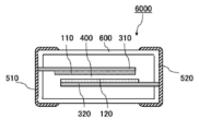
- FIG. 1 is a cross-sectional view of the power storage device 1000 according to the first embodiment.
- the power storage device 1000 is an all-solid-state battery.
- the "storage device 1000" may be referred to as a "battery 1000".
- the first external electrode and the second external electrode may be generically referred to as "terminal electrodes”.
- the first internal electrode may be referred to as a first current collector, and the second internal electrode may be referred to as a second current collector.
- the power storage device 1000 includes a solid electrolyte layer 400, a coating layer 600, a first internal electrode 310, a first external electrode 510, a second internal electrode 320, and a second external electrode 520.
- the first internal electrode 310 is arranged inside the solid electrolyte layer 400.
- the first external electrode 510 is electrically connected to the first internal electrode 310 outside the solid electrolyte layer 400.
- the second internal electrode 320 is arranged inside the solid electrolyte layer 400.
- the second external electrode 520 is electrically connected to the second internal electrode 320 outside the solid electrolyte layer 400.
- the coating layer 600 covers the surface of the solid electrolyte layer 400.
- the coating layer 600 has a lower conductivity than the solid electrolyte layer 400.
- the conductivity of the coating layer 600 may be an order of magnitude or more lower than that of the solid electrolyte layer 400, and may be, for example, 10 -4 S / cm or less.
- the coating layer 600 may be, for example, an insulating layer.
- the power storage device 1000 may include an active material layer arranged inside the solid electrolyte layer 400.
- the power storage device 1000 has a first active material layer 110 which is arranged inside the solid electrolyte layer 400 and on the first internal electrode 310 as an active material layer and is electrically connected to the first external electrode 510. You may. Further, the power storage device 1000 has a second active material layer 120 which is arranged inside the solid electrolyte layer 400 and on the second internal electrode 320 as an active material layer and is electrically connected to the second external electrode 520. You may be doing it.
- the first active material layer 110 may be arranged so as to face the second active material layer 120 with the solid electrolyte layer 400 interposed therebetween.
- the solid electrolyte layer 400 is, for example, a sintered body.
- the solid electrolyte layer 400 include a material having a crystal structure having a garnet structure, a material having a crystal structure having a NASICON type structure, and a material having a perovskite type crystal structure.
- the solid electrolyte layer 400 is, for example, a material having a crystal structure having a garnet structure.
- the solid electrolyte layer 400 is, for example, a sulfur-free material.
- the solid electrolyte layer 400 may include, for example, a crystal phase having Li 7 La 3 Zr 2 O 12 or Li 7 Pr 3 Zr 2 O 12 .
- the insulating property on the surface of the solid electrolyte layer is ensured. Therefore, the plating does not adhere to unnecessary parts other than the terminal electrodes, the terminal electrodes can be plated, and a surface mount type power storage device can be realized.
- the coating layer 600 may contain, for example, an oxide.
- the oxide may include, for example, pyrochlore oxide.
- the pyrochlore oxide may contain, for example, La 2 Zr 2 O 7 or Pr 2 Zr 2 O 7 .
- the coating layer 600 may include, for example, a crystal phase having Li 2 ZrO 3 .
- the coating layer 600 may have a Li-containing molar ratio smaller than that of the solid electrolyte layer 400.
- the thickness of the coating layer 600 is 1 ⁇ m or more and 100 ⁇ m or less.
- the thickness of the coating layer 600 is smaller than 1 ⁇ m, the coating layer elutes into the plating solution when the plating layer is formed on the terminal electrodes, and the insulating property on the surface of the solid electrolyte layer cannot be ensured.
- moisture easily penetrates from the surface of the solid electrolyte layer, so that the moisture resistance is lowered.
- the thickness of the coating layer 600 is larger than 100 ⁇ m, the coating layer is cracked or peeled by the thermal cycle or handling, so that the insulating property on the surface of the solid electrolyte layer cannot be ensured.
- the thickness of the coating layer 600 may be, for example, 5 ⁇ m or more and 100 ⁇ m or less.
- the coating layer can be left even if the sintered element is barrel-polished.
- the surface of the sintered body element can be smoothed and the squares and ridges can be chamfered, so that the bending strength of the sintered body element can be improved and chipping can be suppressed.
- the solid electrolyte layer 400 and the coating layer 600 may have similar constituent elements. Further, both the solid electrolyte layer 400 and the coating layer 600 may be oxides. That is, the solid electrolyte layer 400 may contain a crystal phase having Li 7 La 3 Zr 2 O 12 or Li 7 Pr 3 Zr 2 O 12 , and the coating layer 600 may contain an oxide of the solid electrolyte layer 400. In this case, the oxide of the solid electrolyte layer 400 may include at least one of pyrochlore oxide (for example, La 2 Zr 2 O 7 or Pr 2 Zr 2 O 7 ) or Li 2 ZrO 3 .
- pyrochlore oxide for example, La 2 Zr 2 O 7 or Pr 2 Zr 2 O 7
- the bonding interface between the solid electrolyte layer 400 and the coating layer 600 has a close coefficient of thermal expansion and high consistency, the thermal impact resistance is high as compared with the case where the solid electrolyte is coated with resin or glass. Therefore, at the time of solder mounting, the generation of cracks at the interface is suppressed, the heat resistance is also excellent, and it is possible to cope with surface mounting.
- Heat resistance means durability against heat treatment during so-called solder reflow. In addition, it is also excellent in thermal stress such as a cold cycle in actual use. Due to this action and effect, it is possible to realize surface mounting and high reliability.
- the pre-sintered formed form element of the solid electrolyte layer 400 is sintered or heat-treated.
- the coating layer 600 containing the pyrochlor oxide can be formed at the same time.
- both are formed without voids by the continuous bonding interface diffused from each other. Therefore, as compared with the one in which the surface of the sintered element is coated with a resin, the one having a high bonding strength can be obtained because it is firmly bonded by the sintered structure. Due to this action and effect, high environmental resistance can be obtained without causing a problem that the plating solution or water infiltrates the bonding interface.
- the terminal electrodes can be plated, and the surface has excellent environmental resistance such as impact and cold heat, as shown in FIG. It is possible to realize a power storage device that supports mounting.
- the coating layer 600 may contain a crystal phase having Li 2 ZrO 3, which has a lower conductivity than the crystal phase having a garnet structure. As a result, the coating layer 600 having high adhesion to the solid electrolyte layer 400 is formed, so that the coating layer 600 having excellent environmental resistance such as impact and cold heat can be similarly obtained. Further, the Li-containing molar ratio in the coating layer 600 may be smaller than the Li-containing molar ratio in the solid electrolyte layer 400. By making the Li-containing molar ratio in the coating layer 600 smaller than the Li-containing molar ratio in the solid electrolyte layer 400, the conductivity can be lowered by reducing the carriers. As a result, the same effect as described above can be obtained as the coating layer 600.
- the terminal electrodes can be plated, and a surface mount type power storage device can be realized.
- a sintered body of the solid electrolyte layer 400, a first internal electrode 310 included as a current collector inside the sintered body, a second internal electrode 320, and a coating layer 600 are combined.
- the element is referred to as a sintered element.
- the sintered body element is formed by, for example, a solid solution composition having a garnet structure of Li 7 La 3 Zr 2 O 12 or Li 7 Pr 3 Zr 2 O 12 , and a coating layer 600 covering the surface thereof.
- the solid electrolyte layer 400 in the first embodiment is an oxide-based solid electrolyte, it does not have to contain sulfur unlike the sulfide-based solid electrolyte. Therefore, the sintered element made of the solid electrolyte material of the first embodiment can realize high stability without generating hydrogen sulfide when exposed to the atmosphere or moisture. Therefore, it can be applied to a power storage device that can be manufactured and used in the atmosphere. Further, the sintered body element can be used even if it is impregnated in a plating solution.
- the crystal phase contained in the solid electrolyte layer 400 in the first embodiment may have a garnet-type crystal structure.
- the crystal phase may have a dense and highly conductive cubic system. Further, the crystal phase may have a tetragonal system.
- the solid electrolyte layer having the garnet structure may contain elements other than La and Pr in order to achieve some purposes.
- One of several purposes is to improve the denseness of the solid electrolyte layer 400.
- Another one of some purposes is to realize integral sintering as a laminate with a first current collector, a second current collector, and the like.
- Another one of several purposes is to adjust the shrinkage properties with respect to sintering temperature.
- examples of other elements include elements such as Al, Nb, Ta, and Bi, and rare earth elements such as La, Nd, and Sm.
- the solid electrolyte layer 400 may contain a crystal phase having a crystal structure other than the garnet type as long as the conductivity and atmospheric stability are not impaired.
- the solid electrolyte layer 400 may contain, for example, a pyrochlore phase having high atmospheric stability (for example, Pr 2 Zr 2 O 7 ).
- the crystal structure contained can be confirmed from the X-ray diffraction pattern of the sample cross section. Since the volume ratio occupied by the coating layer 600 is very small when viewed from the entire sintered element, the crystal phase can be sufficiently determined from the diffraction pattern of the entire cross section. For strictness, the XRD pattern in the local region or the diffraction pattern of the sample from which the coating layer 600 has been removed is effective.
- the solid electrolyte layer 400 may contain a conductive auxiliary agent for the purpose of increasing the electronic conductivity.
- a conductive auxiliary agent for the purpose of increasing the electronic conductivity.
- natural graphite, graphite such as artificial graphite, carbon black such as acetylene black and Ketjen black, conductive fibers such as carbon fiber and metal fiber, metal powder such as carbon fluoride and aluminum powder, zinc oxide whisker , Conductive whiskers such as potassium titanate whisker, conductive metal oxides such as titanium oxide, conductive polymer compounds such as polyaniline, polypyrrole, and polythiophene can be used.
- the surface of the sintered body of the solid electrolyte layer 400 mainly having a garnet structure is provided with the end portions (end faces connected to the terminal electrodes) of the first internal electrode 310 and the second internal electrode 320, which are current collectors. Exclude and cover.
- the coating layer 600 is, for example, an oxide having a pyrochlore structure having a lower conductivity than the solid electrolyte layer 400, and may specifically have La 2 Zr 2 O 7 or Pr 2 Zr 2 O 7. ..
- the pyrochlore oxide constituting the coating layer 600 has low conductivity.
- the present inventors have found that Li 2 ZrO 3 , which precipitates on the surface when the solid electrolyte layer 400 mainly composed of a garnet structure is further oversintered, also has high atmospheric stability and low conductivity. Therefore, when the coating layer 600 contains pyrochlore oxide and Li 2 ZrO 3 , a high action effect as the coating layer 600 can be obtained.
- the coating layer 600 has, for example, an action effect of not adhering plating to unnecessary parts other than the terminal electrodes.
- the sintered element is dense (density> 4.0 g / cm 3 ) and stable to the atmosphere and moisture, it is highly durable against impregnation of the plating solution and collision between the elements in the manufacturing process. is there.
- the coating layer 600 may contain elements other than La and Pr.
- elements include elements that are easily incorporated into a garnet structure or a pyrochlore structure, such as Al, Nb, Ta, and Bi, and rare earth elements such as La, Nd, and Sm.
- the molar ratio of Li element in the coating layer 600 may be smaller than the molar ratio of Li content in the solid electrolyte layer. That is, by evaporating the distribution of the surface layer of the conductive carrier (Li ion) by the firing process conditions or heat treatment, the coating layer 600 can be formed even if it has a garnet structure by reducing the distribution from the inside.
- the coating layer 600 in the present disclosure is obtained by, for example, forming an oxide in the surface layer region of the solid electrolyte layer 400 by selectively evaporating Li when the solid electrolyte layer 400 is oversintered. ..
- the crystal structure of the coating layer 600 can also be confirmed from the XRD pattern of the sample processed only in the local region or the high resistance layer, similarly to the solid electrolyte layer 400.
- the pyrochlore oxide is formed on the surface layer by selectively evaporating Li on the surface layer in the sintering process of the solid solution composition having a garnet structure. For example, by applying a heat treatment of a solid electrolyte sintered body having a garnet structure at 700 ° C. to 1300 ° C. for 10 minutes to 60 minutes in the air, pyrochlore oxide can be produced only in the surface layer region.
- a power storage device in which a stable coating layer 600 having a thickness of 1 ⁇ m or more and 100 ⁇ m or less and a solid electrolyte layer 400 are integrated.
- the coating layer 600 can be formed over a wide range and thickly.
- the thickness of the coating layer 600 can be controlled by the temperature and the treatment time, and the coating layer 600 can be formed thicker by increasing the temperature or the treatment time.
- a heat-resistant container having good air permeability may be used.
- the heat-resistant container may be a container made of alumina having a porosity of 30% or more and 60% or less in order to enhance air permeability.
- the uneven shape of the surface may be embossed with a thickness of about 50 ⁇ m.
- the sintered element is chamfered for the purpose of preventing chipping or improving mechanical strength.
- chamfering may be performed by barrel polishing or the like, and then terminal electrodes may be formed and plated. Therefore, the thickness of the coating layer 600 may be, for example, 5 ⁇ m or more.
- a water repellent treatment agent such as a silane coupling agent may be applied before plating in order to completely prevent the plating solution from entering the sintered body element.
- the thickness of the coating layer 600 can be evaluated by an optical microscope or SEM from the observation of its cross section. For example, the average value of the thicknesses of any five points in the cross section can be adopted as the thickness of the coating layer 600.
- the conductivity of the coating layer 600 and the inside of the sintered body can be measured by measuring the surface resistance (4 probe measuring method, for example, Loresta-GX manufactured by Mitsubishi Chemical Analytech). Alternatively, it can be evaluated by a nanoprober system (Hitachi, Ltd.) used for failure analysis of semiconductor devices such as LSI.
- a metal having high conductivity can be used for the first internal electrode 310 and the second internal electrode 320, which are current collectors in the inner layer of the sintered body element.
- metals such as Pd, Pt, Ag, Cu and Ni, alloys such as Ag-Pd and Ag-Pt, and the like can be used.
- any metal having a melting point of the first internal electrode 310 and the second internal electrode 320 equal to or higher than the sintering temperature of the solid electrolyte layer 400 can be used.
- base metals such as Cu and Ni are used, they can be used as an internal electrode that is a current collector by controlling the partial pressure of oxygen that does not oxidize the electrode and firing it.
- the firing shrinkage rate may be controlled in order to improve the problem that the interface between the electrode metal and its surroundings is peeled off in the sintering process due to the difference in shrinkage characteristics.
- an additive that is diffused and bonded to the surroundings may be contained within a range that does not impair the conductivity.
- a solid electrolyte to be bonded a positive electrode and a negative electrode active material can be used.
- various metals and oxides can be used. Those having a particle size equal to or less than the electrode thickness can be used.
- the terminal electrode is composed of a metal showing high conductivity. Specifically, Ag, Cu, Ni, Pt, Pd, Ag-Pd, Ag-Pt and the like can be used. Usually, a paste of metal powder is applied to the end face of the sintered body to be baked to secure an electrical connection with an internal electrode which is a current collector.
- a terminal electrode having high adhesion strength can be formed by containing a glass frit and diffusing it into the sintered body element. Further, since the effect of closing the pores in the baked electrode structure with the glass component can be obtained, a sealing effect can be obtained to prevent moisture such as a plating solution from entering the inside of the sintered body element and deteriorating the characteristics. ..
- a glass component contained in the terminal electrode By baking such a glass component contained in the terminal electrode at the softening point or higher, the surface of the coating layer 600 is wetted and spread by the capillary phenomenon, and the infiltration route or pores of the coating layer 600 are formed. It is possible to obtain a sealing effect for the entire sintered body element.
- the glass component when the glass component is directly diffused into the solid electrolyte layer, it is rapidly diffused into the inside of the sintered body through the grain boundaries having a high diffusion rate, and the conductivity may be deteriorated because the conductive path is blocked. ..
- the coating layer 600 as the diffusion layer of the glass frit and the protective layer of the solid electrolyte layer 400, deterioration of the conductivity of the functional portion can be suppressed. Due to these actions and effects, it is possible to obtain a high-performance power storage device while obtaining high reliability even for deflection stress, drop impact, environmental resistance test, etc. after mounting on the substrate.
- the "functional portion" is, for example, a region sandwiched between a positive electrode and a negative electrode.
- Environmental resistance tests include, for example, tests to determine durability against moisture.
- the first active material layer 110 can be used as the positive electrode.
- the first active material layer 110 used as the positive electrode contains a material having the property of occluding and releasing metal ions.
- An example of a metal ion is lithium ion.
- the positive electrode contains, for example, a positive electrode active material.
- the positive electrode may include the solid electrolyte layer 400. In addition to forming a conductive path, it is effective in controlling the firing shrinkage rate or improving structural defects when the positive electrode active material and the solid electrolyte layer 400 are simultaneously sintered, and as the effect, high energy density and discharge capacity are imparted. Can be done.
- the second active material layer 120 can be used as the negative electrode.
- the second active material layer 120 as the negative electrode contains a material having the property of occluding and releasing metal ions.
- An example of a metal ion is lithium ion.
- the negative electrode may contain, for example, a negative electrode active material and a solid electrolyte, and is effective for controlling the firing shrinkage rate or improving structural defects when the negative electrode active material and the solid electrolyte are simultaneously sintered. The same effect as in the case of is obtained.
- At least one selected from the positive electrode and the negative electrode may contain a conductive auxiliary agent for the purpose of enhancing electronic conductivity.
- the device can function as a solid capacitor.
- An embodiment of the solid capacitor is as shown in FIG.
- the terminal electrodes are plated with Ni (base) -Sn (surface layer).
- the thickness of the plating layer is 1 ⁇ m or more and 5 ⁇ m or less, respectively.
- the total thickness of the Ni layer and the Sn layer may be, for example, 1 ⁇ m or more and 10 ⁇ m or less.
- the solid electrolyte material having a garnet structure according to the first embodiment can be produced, for example, by the following method.
- Li 2 CO 3 powder, Pr 6 O 11 powder, and Zr O 2 powder are prepared as starting materials. Subsequently, each raw material powder is weighed so that the desired, for example, solid electrolyte layer has the composition of Li 7 Pr 3 Zr 2 O 12 . Even if an intermediate phase Pr-based pyrochlore oxide (for example, Pr 2 Zr 2 O 7 ) produced by calcining is synthesized in advance and this precursor is used as a starting material, garnet is similarly used during sintering. The structure can be obtained.
- Pr-based pyrochlore oxide for example, Pr 2 Zr 2 O 7
- composition ratio of the three components does not have to be a stoichiometric composition, as long as it forms a solid solution having a cubic garnet structure and is densely sintered (for example, has a density of 4.0 g / cm 3 or more).
- This dried calcined powder After crushing, it is sufficiently dehydrated and dried. By sintering this dried calcined powder, a solid electrolyte layer 400 having a garnet structure is synthesized. This calcined pulverized powder can be used to make a power storage device by a general laminating process.
- the calcined powder is weighed as the raw material of the solid electrolyte layer 400, and an organic binder such as butyl resin, a solvent mainly composed of butyl acetate, and a plasticizer such as BBP are added and mixed and dispersed.
- the obtained slurry is mesh-passed to remove agglomerates and lumps of binder, and then molded on a 50 ⁇ m PET film by a doctor blade method to prepare a green sheet.
- the active material layers of the positive and negative electrodes are formed by a screen printing method using the first and second active material paces.
- the green sheet on which the printed body is formed is laminated and pressed so as to have a desired configuration, and the laminated body is formed. obtain.
- This laminated body is cut and separated into desired dimensions to obtain individual raw chip elements.
- This raw chip element is placed in a heat-resistant alumina sheath, and zirconia bedding powder (average particle size 50 ⁇ m) is uniformly sprayed so that the molded body and the bottom of the sheath do not come into direct contact with each other, and then fired.
- the molded product is placed and embedded in the calcined powder of the same composition.
- the debinder treatment is performed by heating at about 400 ° C. to 500 ° C. for 2 to 5 hours in a nitrogen flow. After that, a sheath lid smoothed with # 800 is placed and sealed, and sintered at 1050 ° C to 1130 ° C for 2 to 10 hours. After that, the sheath lid is released and heat-treated at the same temperature as the firing temperature for 5 to 30 minutes.
- Li can be selectively evaporated, and the coating layer 600 can be formed in the surface layer region of the solid electrolyte layer 400.
- a sintered body element to be the power storage device of the present invention is obtained.
- the internal electrode is a metal that does not oxidize in the atmosphere, such as AgPd (silver-palladium), the baking atmosphere may be in the atmosphere.
- the terminal electrodes are plated by means such as barrel plating, which is generally applied to the terminal electrodes of chip components, to obtain the power storage device 2000 shown in FIG.
- an active material that can be charged and discharged can be used, and a solid electrolyte may be contained as a mixture component.
- the solid electrolyte as a mixture is not limited to the garnet structure. It can be used as long as it does not cause structural defects and unnecessary reactions by simultaneous sintering. Further, when it is applied as a solid ion capacitor, it can be manufactured by simultaneously firing a current collector as an internal electrode with the same configuration as a normal laminated capacitor without forming the above-mentioned active material layer.
- FIG. 2 is a schematic view illustrating the configuration of the power storage device according to the second embodiment.
- FIG. 2 is a cross-sectional view of the power storage device 2000 according to the present embodiment.
- Elements common to the power storage device 1000 of the first embodiment and the power storage device 2000 of the present embodiment are designated by the same reference numerals, and the description thereof may be omitted. That is, the following description of each embodiment can be applied to each other as long as there is no technical contradiction. Moreover, the embodiments may be combined with each other as long as they are not technically inconsistent.
- the power storage device 2000 further includes plating that covers the surfaces of the first external electrode 510 and the second external electrode 520. As shown in FIG. 2, the power storage device 2000 has a first plating layer 710 on the first external electrode 510 and a second plating layer 720 on the second external electrode 520.
- the plating layer may have a plurality of layers having two or more layers having a base layer. Examples of the metal forming the base layer of the plating layer include Cu, Ni, Ag, Pd, Sn, Au and alloys thereof. These may be used alone or in combination of two or more.
- the base layer of the plating layer may be, for example, Ni and a Ni alloy.
- the surface layer of the plating layer includes Cu, Ni, Ag, Au, Sn, Zn and alloys thereof. These may be used alone or in combination of two or more.
- the surface layer of the plating layer may be, for example, Sn and Sn alloy.
- the plating layer may be, for example, Ni (base) -Sn (surface layer).
- the plating method is not particularly limited, and a known method can be used.
- FIG. 3 is a schematic view illustrating the configuration of the power storage device according to the third embodiment.
- FIG. 3 is a cross-sectional view of the power storage device 3000 according to the present embodiment.
- Elements common to the power storage device 1000 of the first embodiment and the power storage device 3000 of the present embodiment are designated by the same reference numerals, and their description may be omitted. That is, the following description of each embodiment can be applied to each other as long as there is no technical contradiction. Moreover, the embodiments may be combined with each other as long as they are not technically inconsistent.
- the power storage device 3000 according to this embodiment can be applied as a capacitor.
- the power storage device 3000 does not have an active material layer such as the first active material layer 110 and the second active material layer 120.
- the terminal electrodes can be plated, and a surface mount type power storage device can be realized.
- FIG. 4 is a schematic view illustrating the configuration of the power storage device according to the fourth embodiment.
- FIG. 4 is a cross-sectional view of the power storage device 4000 according to the present embodiment.
- Elements common to the power storage device 1000 of the first embodiment and the power storage device 4000 of the present embodiment are designated by the same reference numerals, and the description thereof may be omitted. That is, the following description of each embodiment can be applied to each other as long as there is no technical contradiction. Moreover, the embodiments may be combined with each other as long as they are not technically inconsistent.
- the first external electrode 510 and the second external electrode 520 are shaped so as to cover a part of the periphery of the solid electrolyte layer 400.
- the shape of the first external electrode 510 is not particularly limited as long as it is electrically connected to the first active material layer 110 and the first internal electrode 310.
- the shape of the second external electrode 520 is not particularly limited as long as it is electrically connected to the second active material layer 120 and the second internal electrode 320.
- the terminal electrodes can be plated, and a surface mount type power storage device can be realized.
- FIG. 5 is a schematic view illustrating the configuration of the power storage device according to the fifth embodiment.
- FIG. 5 is a cross-sectional view of the power storage device 5000 according to the present embodiment.
- Elements common to the power storage device 1000 of the first embodiment and the power storage device 5000 of the present embodiment are designated by the same reference numerals, and their description may be omitted. That is, the following description of each embodiment can be applied to each other as long as there is no technical contradiction. Moreover, the embodiments may be combined with each other as long as they are not technically inconsistent.
- the power storage device 5000 includes a plurality of cells.
- the power storage device 5000 includes a plurality of cells electrically connected in parallel.
- the plurality of cells are electrically connected to the first internal electrode 310 and the second active material layer 120, which are electrically connected to the first active material layer 110, the second active material layer 120, and the first active material layer 110, respectively.
- the second internal electrode 320 and the solid electrolyte layer 400 are provided.
- Each of the cells has two pairs of paired end faces facing each other.
- the power storage device 5000 is configured by stacking a plurality of cells 30.
- the terminal electrodes can be plated, and a surface mount type power storage device can be realized.
- FIG. 6 is a schematic view illustrating the configuration of the power storage device according to the sixth embodiment.
- FIG. 6 is a cross-sectional view of the power storage device 6000 according to the present embodiment.
- Elements common to the power storage device 1000 of the first embodiment and the power storage device 6000 of the present embodiment are designated by the same reference numerals, and their description may be omitted. That is, the following description of each embodiment can be applied to each other as long as there is no technical contradiction. Moreover, the embodiments may be combined with each other as long as they are not technically inconsistent.
- the first active material layer 110 is not in contact with the first external electrode 510. That is, in the power storage device 6000, the first active material layer 110 is arranged inside the solid electrolyte layer 400 and on the first internal electrode 310, but is physically separated from the first external electrode 510. Further, in the power storage device 6000, the second active material layer 120 is not in contact with the second external electrode 520. That is, in the power storage device 6000, the second active material layer 120 is arranged inside the solid electrolyte layer 400 and on the second internal electrode 320, but is physically separated from the second external electrode 520.
- the shape of the first external electrode 510 is not particularly limited as long as it is electrically connected to the first internal electrode 310.
- the shape of the second external electrode 520 is not particularly limited as long as it is electrically connected to the second internal electrode 320.
- FIG. 7 is a schematic view illustrating the configuration of the power storage device according to the seventh embodiment.
- FIG. 7 is a cross-sectional view of the power storage device 7000 according to the present embodiment.
- Elements common to the power storage device 1000 of the first embodiment and the power storage device 7000 of the present embodiment are designated by the same reference numerals, and their description may be omitted. That is, the following description of each embodiment can be applied to each other as long as there is no technical contradiction. Moreover, the embodiments may be combined with each other as long as they are not technically inconsistent.
- the power storage device 7000 further includes a resin electrode that covers the surfaces of the first external electrode 510 and the second external electrode 520. As shown in FIG. 7, the power storage device 7000 further has a first resin electrode 810 on the surface of the first external electrode 510, and further has a second resin electrode 820 on the surface of the second external electrode 520.
- the first resin electrode 810 and the second resin electrode 820 may have a Young's modulus lower than, for example, the first external electrode 510 and the second external electrode 520.
- the first resin electrode 810 and the second resin electrode 820 may be, for example, a conductive resin.
- the material contained in the conductive resin is not particularly limited, and known materials can be used.
- the method for forming the first resin electrode 810 and the second resin electrode 820 is not particularly limited, and known methods can be used. Although not shown in FIG. 7, the power storage device 7000 has a plating layer on the surface of the first external electrode 510 and the second external electrode 520, or on the surface of the first resin electrode 810 and the second resin electrode 820. You may.
- the battery using the solid electrolyte of the present disclosure is useful as a power storage device used for various electronic air devices.
Abstract
The present invention provides a surface-mounted power storage device. This power storage device includes: a solid electrolyte layer (400); a coating layer (600) that coats a surface of the solid electrolyte layer (400); a first inner electrode (310) disposed inside the solid electrolyte layer (400); a first outer electrode (510) electrically connected to the first inner electrode (310) outside the solid electrolyte layer (400); a second inner electrode (320) disposed inside the solid electrolyte layer (400); and a second outer electrode (520) electrically connected to the second inner electrode (320) outside the solid electrolyte layer (400). The coating layer (600) has a conductivity that is lower than that of the solid electrolyte layer (400).
Description
本開示は、固体電解質を用いた蓄電デバイスに関する。
The present disclosure relates to a power storage device using a solid electrolyte.
特許文献1には、ガーネット型結晶Li7L3Zr2O12からなる固体電解質構造体の表面を樹脂で被覆した電池が開示されている。特許文献2には、固体電解質としてLi7La3Zr2O12を用い、正極あるいは負極と固体電解質との間に絶縁層を用いた電池が開示されている。
Patent Document 1 discloses a battery in which the surface of a solid electrolyte structure made of garnet-type crystal Li 7 L 3 Zr 2 O 12 is coated with a resin. Patent Document 2 discloses a battery in which Li 7 La 3 Zr 2 O 12 is used as the solid electrolyte and an insulating layer is used between the positive electrode or the negative electrode and the solid electrolyte.
本開示は、表面実装型の蓄電デバイスを提供することを目的とする。
The present disclosure aims to provide a surface mount type power storage device.
本開示は、
固体電解質層と、
前記固体電解質層の表面を被覆する被覆層と、
前記固体電解質層の内部に配置された第1内部電極と、
前記固体電解質層の外部において前記第1内部電極と電気的に接続される第1外部電極と、
前記固体電解質層の内部に配置された第2内部電極と、
前記固体電解質層の外部において前記第2内部電極と電気的に接続される第2外部電極と、を備え、
前記被覆層は、前記固体電解質層よりも低い導電率を有し、
前記被覆層は、1μm以上100μm以下の厚さを有する、
蓄電デバイスを提供する。 This disclosure is
With a solid electrolyte layer,
A coating layer that covers the surface of the solid electrolyte layer and
The first internal electrode arranged inside the solid electrolyte layer and
A first external electrode electrically connected to the first internal electrode outside the solid electrolyte layer,
A second internal electrode arranged inside the solid electrolyte layer,
A second external electrode that is electrically connected to the second internal electrode outside the solid electrolyte layer is provided.
The coating layer has a lower conductivity than the solid electrolyte layer and has a lower conductivity.
The coating layer has a thickness of 1 μm or more and 100 μm or less.
Provides a power storage device.
本開示によれば、表面実装型の蓄電デバイスを提供できる。
According to the present disclosure, a surface mount type power storage device can be provided.
(本開示の一態様の概要)
本開示の第1態様にかかる蓄電デバイスは、
固体電解質層と、
前記固体電解質層の表面を被覆する被覆層と、
前記固体電解質層の内部に配置された第1内部電極と、
前記固体電解質層の外部において前記第1内部電極と電気的に接続される第1外部電極と、
前記固体電解質層の内部に配置された第2内部電極と、
前記固体電解質層の外部において前記第2内部電極と電気的に接続される第2外部電極と、
を備え、
前記被覆層は、前記固体電解質層よりも低い導電率を有し、
前記被覆層は、1μm以上100μm以下の厚さを有する。 (Summary of one aspect of the present disclosure)
The power storage device according to the first aspect of the present disclosure is
With a solid electrolyte layer,
A coating layer that covers the surface of the solid electrolyte layer and
The first internal electrode arranged inside the solid electrolyte layer and
A first external electrode electrically connected to the first internal electrode outside the solid electrolyte layer,
A second internal electrode arranged inside the solid electrolyte layer,
A second external electrode electrically connected to the second internal electrode outside the solid electrolyte layer,
With
The coating layer has a lower conductivity than the solid electrolyte layer and has a lower conductivity.
The coating layer has a thickness of 1 μm or more and 100 μm or less.
第1態様によれば、固体電解質層の表面の絶縁性が確保される。このため、端子メッキ処理を行う場合に、端子以外の部分にメッキが析出することを抑制できる。これにより、半田実装に対応した蓄電デバイスを提供できる。
According to the first aspect, the insulating property of the surface of the solid electrolyte layer is ensured. Therefore, when the terminal plating process is performed, it is possible to prevent the plating from being deposited on a portion other than the terminals. This makes it possible to provide a power storage device compatible with solder mounting.
本開示の第2態様において、例えば、第1態様にかかる蓄電デバイスでは、さらに、前記固体電解質層の内部に配置された活物質層を備えてもよい。このような構成によれば、半田実装に対応した蓄電デバイスを提供できる。
In the second aspect of the present disclosure, for example, the power storage device according to the first aspect may further include an active material layer arranged inside the solid electrolyte layer. According to such a configuration, it is possible to provide a power storage device compatible with solder mounting.
本開示の第3態様において、例えば、第1又は第2態様にかかる蓄電デバイスでは、前記固体電解質層は、焼結体であってもよい。このような構成によれば、半田実装に対応した蓄電デバイスを提供できる。
In the third aspect of the present disclosure, for example, in the power storage device according to the first or second aspect, the solid electrolyte layer may be a sintered body. According to such a configuration, it is possible to provide a power storage device compatible with solder mounting.
本開示の第4態様において、例えば、第1から第3態様のいずれか1つにかかる蓄電デバイスでは、前記固体電解層質は、ガーネット構造を有していてもよい。このような構成によれば、半田実装に対応した蓄電デバイスを提供できる。
In the fourth aspect of the present disclosure, for example, in the power storage device according to any one of the first to third aspects, the solid electrolytic layer may have a garnet structure. According to such a configuration, it is possible to provide a power storage device compatible with solder mounting.
本開示の第5態様において、例えば、第1から第4態様のいずれか1つにかかる蓄電デバイスでは、前記固体電解質層は、硫黄を含まないものであってもよい。このような構成によれば、半田実装に対応した蓄電デバイスを提供できる。
In the fifth aspect of the present disclosure, for example, in the power storage device according to any one of the first to fourth aspects, the solid electrolyte layer may not contain sulfur. According to such a configuration, it is possible to provide a power storage device compatible with solder mounting.
本開示の第6態様において、例えば、第1から第5態様のいずれか1つにかかる蓄電デバイスでは、前記固体電解質層は、Li7La3Zr2O12およびLi7Pr3Zr2O12からなる群から選択される少なくとも1つを有する結晶相を含んでいてもよい。このような構成によれば、半田実装に対応した蓄電デバイスを提供できる。
In the sixth aspect of the present disclosure, for example, in the power storage device according to any one of the first to fifth aspects, the solid electrolyte layer is Li 7 La 3 Zr 2 O 12 and Li 7 Pr 3 Zr 2 O 12. It may contain a crystal phase having at least one selected from the group consisting of. According to such a configuration, it is possible to provide a power storage device compatible with solder mounting.
本開示の第7態様において、例えば、第1から第6態様のいずれか1つにかかる蓄電デバイスでは、前記被覆層は、10-4S/cm以下の導電率を有していてもよい。このような構成によれば、半田実装に対応した蓄電デバイスを提供できる。
In the seventh aspect of the present disclosure, for example, in the power storage device according to any one of the first to sixth aspects, the coating layer may have a conductivity of 10 -4 S / cm or less. According to such a configuration, it is possible to provide a power storage device compatible with solder mounting.
本開示の第8態様において、例えば、第1から第7態様のいずれか1つにかかる蓄電デバイスでは、前記被覆層は、酸化物を含んでいてもよい。このような構成によれば、半田実装に対応した蓄電デバイスを提供できる。
In the eighth aspect of the present disclosure, for example, in the power storage device according to any one of the first to seventh aspects, the coating layer may contain an oxide. According to such a configuration, it is possible to provide a power storage device compatible with solder mounting.
本開示の第9態様において、例えば、第8態様にかかる蓄電デバイスでは、前記酸化物は、パイロクロア酸化物を含んでいてもよい。このような構成によれば、半田実装に対応した蓄電デバイスを提供できる。
In the ninth aspect of the present disclosure, for example, in the power storage device according to the eighth aspect, the oxide may contain a pyrochlore oxide. According to such a configuration, it is possible to provide a power storage device compatible with solder mounting.
本開示の第10態様において、例えば、第9態様にかかる蓄電デバイスでは、前記パイロクロア酸化物は、La2Zr2O7およびPr2Zr2O7からなる群から選択される少なくとも1つを含んでいてもよい。このような構成によれば、半田実装に対応した蓄電デバイスを提供できる。
In the tenth aspect of the present disclosure, for example, in the electricity storage device according to the ninth aspect, the pyrochlore oxide contains at least one selected from the group consisting of La 2 Zr 2 O 7 and Pr 2 Zr 2 O 7. You may be. According to such a configuration, it is possible to provide a power storage device compatible with solder mounting.
本開示の第11態様において、例えば、第1から第10態様のいずれか1項に記載された蓄電デバイスでは、前記被覆層は、Li2ZrO3を有する結晶相を含んでいてもよい。このような構成によれば、半田実装に対応した蓄電デバイスを提供できる。
In the eleventh aspect of the present disclosure, for example, in the power storage device according to any one of the first to tenth aspects, the coating layer may contain a crystal phase having Li 2 ZrO 3 . According to such a configuration, it is possible to provide a power storage device compatible with solder mounting.
本開示の第12態様において、例えば、第1から第11態様のいずれか1つにかかる蓄電デバイスでは、前記被覆層は、前記固体電解質層よりも小さいLi含有モル比率を有していてもよい。このような構成によれば、半田実装に対応した蓄電デバイスを提供できる。
In the twelfth aspect of the present disclosure, for example, in the power storage device according to any one of the first to eleventh aspects, the coating layer may have a Li-containing molar ratio smaller than that of the solid electrolyte layer. .. According to such a configuration, it is possible to provide a power storage device compatible with solder mounting.
本開示の第13態様において、例えば、1から第12態様のいずれか1つにかかる蓄電デバイスでは、前記被覆層は、5μm以上100μm以下の厚さを有していてもよい。このような構成によれば、半田実装に対応した蓄電デバイスを提供できる。
In the thirteenth aspect of the present disclosure, for example, in the power storage device according to any one of the first to twelfth aspects, the coating layer may have a thickness of 5 μm or more and 100 μm or less. According to such a configuration, it is possible to provide a power storage device compatible with solder mounting.
本開示の第14態様において、例えば、第1から第13態様のいずれか1つにかかる蓄電デバイスでは、前記第1外部電極及び第2外部電極の表面を被覆するメッキをさらに備えていてもよい。このような構成によれば、半田実装に対応した蓄電デバイスを提供できる。
In the fourteenth aspect of the present disclosure, for example, the power storage device according to any one of the first to thirteenth aspects may further include plating for covering the surfaces of the first external electrode and the second external electrode. .. According to such a configuration, it is possible to provide a power storage device compatible with solder mounting.
本開示の第15態様において、例えば、第1から第14態様のいずれか1つにかかる蓄電デバイスでは、前記メッキは、1μm以上10μm以下の厚さを有していてもよい。このような構成によれば、半田実装に対応した蓄電デバイスを提供できる。
In the fifteenth aspect of the present disclosure, for example, in the power storage device according to any one of the first to the fourteenth aspects, the plating may have a thickness of 1 μm or more and 10 μm or less. According to such a configuration, it is possible to provide a power storage device compatible with solder mounting.
以下、実施の形態について図面を参照しながら具体的に説明する。
Hereinafter, the embodiment will be specifically described with reference to the drawings.
なお、以下で説明する実施の形態は、いずれも包括的又は具体的な例を示すものである。以下の実施形態で示される数値、形状、材料、構成要素、構成要素の配置位置及び接続形態などは、一例であり、本開示を限定する主旨ではない。また、以下の実施の形態における構成要素のうち、最上位概念を示す独立請求項に記載されていない構成要素については、任意の構成要素として説明される。
It should be noted that all of the embodiments described below show comprehensive or specific examples. Numerical values, shapes, materials, components, arrangement positions of components, connection forms, etc. shown in the following embodiments are examples, and are not intended to limit the present disclosure. Further, among the components in the following embodiments, the components not described in the independent claims indicating the highest level concept are described as arbitrary components.
また、各図は、必ずしも厳密に図示したものではない。各図において、実質的に同一の構成については同一の符号を付し、重複する説明は省略又は簡略化する。
Also, each figure is not necessarily exactly illustrated. In each figure, substantially the same configuration is designated by the same reference numerals, and duplicate description is omitted or simplified.
(実施形態1)
[蓄電デバイスの概要]
まず、本実施形態に係る蓄電デバイスについて説明する。 (Embodiment 1)
[Overview of power storage device]
First, the power storage device according to the present embodiment will be described.
[蓄電デバイスの概要]
まず、本実施形態に係る蓄電デバイスについて説明する。 (Embodiment 1)
[Overview of power storage device]
First, the power storage device according to the present embodiment will be described.
蓄電デバイスは、全固体電池であってもよく、キャパシタであってもよい。
The power storage device may be an all-solid-state battery or a capacitor.
図1は、本実施形態1に係る蓄電デバイス1000の断面図である。本実施形態において、蓄電デバイス1000は、全固体電池である。本明細書では、「蓄電デバイス1000」を「電池1000」と呼ぶことがある。また、本明細書では、第1外部電極と第2外部電極とを総称して「端子電極」と呼ぶことがある。また、本明細書では、第1内部電極を第1集電体と呼ぶことがあり、第2内部電極を第2集電体と呼ぶことがある。
FIG. 1 is a cross-sectional view of the power storage device 1000 according to the first embodiment. In this embodiment, the power storage device 1000 is an all-solid-state battery. In the present specification, the "storage device 1000" may be referred to as a "battery 1000". Further, in the present specification, the first external electrode and the second external electrode may be generically referred to as "terminal electrodes". Further, in the present specification, the first internal electrode may be referred to as a first current collector, and the second internal electrode may be referred to as a second current collector.
図1に示すように、蓄電デバイス1000は、固体電解質層400と、被覆層600と、第1内部電極310と、第1外部電極510と、第2内部電極320と、第2外部電極520と、を備える。第1内部電極310は、固体電解質層400の内部に配置されている。第1外部電極510は、固体電解質層400の外部において第1内部電極310と電気的に接続されている。第2内部電極320は、固体電解質層400の内部に配置されている。第2外部電極520は、固体電解質層400の外部において第2内部電極320と電気的に接続されている。被覆層600は、固体電解質層400の表面を被覆している。被覆層600は、固体電解質層400よりも低い導電率を有する。被覆層600の導電率は、固体電解質層400よりも、一桁以上低い導電率であってもよく、例えば、10-4S/cm以下であってもよい。被覆層600は、例えば、絶縁層であってもよい。
As shown in FIG. 1, the power storage device 1000 includes a solid electrolyte layer 400, a coating layer 600, a first internal electrode 310, a first external electrode 510, a second internal electrode 320, and a second external electrode 520. , Equipped with. The first internal electrode 310 is arranged inside the solid electrolyte layer 400. The first external electrode 510 is electrically connected to the first internal electrode 310 outside the solid electrolyte layer 400. The second internal electrode 320 is arranged inside the solid electrolyte layer 400. The second external electrode 520 is electrically connected to the second internal electrode 320 outside the solid electrolyte layer 400. The coating layer 600 covers the surface of the solid electrolyte layer 400. The coating layer 600 has a lower conductivity than the solid electrolyte layer 400. The conductivity of the coating layer 600 may be an order of magnitude or more lower than that of the solid electrolyte layer 400, and may be, for example, 10 -4 S / cm or less. The coating layer 600 may be, for example, an insulating layer.
蓄電デバイス1000は、固体電解質層400の内部に配置された活物質層を備えていてもよい。蓄電デバイス1000は、活物質層として、固体電解質層400の内部、かつ第1内部電極310上に配置され、第1外部電極510と電気的に接続される第1活物質層110を有していてもよい。また、蓄電デバイス1000は、活物質層として、固体電解質層400の内部、かつ第2内部電極320上に配置され、第2外部電極520と電気的に接続される第2活物質層120を有していてもよい。第1活物質層110は、固体電解質層400を挟んで第2活物質層120と対向するように配置されていてもよい。
The power storage device 1000 may include an active material layer arranged inside the solid electrolyte layer 400. The power storage device 1000 has a first active material layer 110 which is arranged inside the solid electrolyte layer 400 and on the first internal electrode 310 as an active material layer and is electrically connected to the first external electrode 510. You may. Further, the power storage device 1000 has a second active material layer 120 which is arranged inside the solid electrolyte layer 400 and on the second internal electrode 320 as an active material layer and is electrically connected to the second external electrode 520. You may be doing it. The first active material layer 110 may be arranged so as to face the second active material layer 120 with the solid electrolyte layer 400 interposed therebetween.
このような構成により、端子電極以外の余計な箇所にメッキを付着させずに、選択的に端子電極へのメッキ処理が可能になり、表面実装型の蓄電デバイスとしての基本構成を実現できる。
With such a configuration, it is possible to selectively plate the terminal electrodes without attaching plating to unnecessary parts other than the terminal electrodes, and it is possible to realize a basic configuration as a surface mount type power storage device.
固体電解質層400は、例えば、焼結体である。固体電解質層400としては、ガーネット構造の結晶構造を有する材料、NASICON型構造を有する結晶構造を有する材料、ペロブスカイト型の結晶構造を有する材料などが挙げられる。固体電解質層400は、例えば、ガーネット構造の結晶構造を有する材料である。固体電解質層400は、例えば、硫黄を含まない材料である。固体電解質層400は、例えば、Li7La3Zr2O12又はLi7Pr3Zr2O12を有する結晶相を含んでいてもよい。
The solid electrolyte layer 400 is, for example, a sintered body. Examples of the solid electrolyte layer 400 include a material having a crystal structure having a garnet structure, a material having a crystal structure having a NASICON type structure, and a material having a perovskite type crystal structure. The solid electrolyte layer 400 is, for example, a material having a crystal structure having a garnet structure. The solid electrolyte layer 400 is, for example, a sulfur-free material. The solid electrolyte layer 400 may include, for example, a crystal phase having Li 7 La 3 Zr 2 O 12 or Li 7 Pr 3 Zr 2 O 12 .
以上の構成によれば、固体電解質層の表面の絶縁性が確保される。このため、端子電極以外の余計な箇所にメッキが付着せず、端子電極のメッキ対応が可能になり、表面実装型の蓄電デバイスを実現できる。
According to the above configuration, the insulating property on the surface of the solid electrolyte layer is ensured. Therefore, the plating does not adhere to unnecessary parts other than the terminal electrodes, the terminal electrodes can be plated, and a surface mount type power storage device can be realized.
被覆層600は、例えば、酸化物を含んでいてもよい。酸化物は、例えば、パイロクロア酸化物を含んでいてもよい。パイロクロア酸化物は、例えば、La2Zr2O7又はPr2Zr2O7を含んでいてもよい。被覆層600は、例えば、Li2ZrO3を有する結晶相を含んでいてもよい。被覆層600は、固体電解質層400よりも小さいLi含有モル比率を有していてもよい。
The coating layer 600 may contain, for example, an oxide. The oxide may include, for example, pyrochlore oxide. The pyrochlore oxide may contain, for example, La 2 Zr 2 O 7 or Pr 2 Zr 2 O 7 . The coating layer 600 may include, for example, a crystal phase having Li 2 ZrO 3 . The coating layer 600 may have a Li-containing molar ratio smaller than that of the solid electrolyte layer 400.
被覆層600の厚さは、1μm以上100μm以下である。被覆層600の厚さが1μmよりも小さい場合、端子電極上にメッキ層を形成する際に被覆層がメッキ液中に溶出してしまい、固体電解質層の表面の絶縁性が確保されなくなる。また、固体電解質層の表面から水分が侵入しやすくなるため、耐湿性が低下する。被覆層600の厚さが100μmよりも大きい場合、冷熱サイクル又はハンドリングにより被覆層の割れ又は剥離が生じるため、固体電解質層の表面の絶縁性が確保されなくなる。また、被覆層600の厚さは、例えば、5μm以上100μm以下であってもよい。被覆層600の厚さが5μm以上である場合、焼結体素子をバレル研磨しても、被覆層を残存させることができる。これにより、焼結体素子の表面の平滑化、および、4角および稜線の面取りが可能となるため、焼結体素子の抗折強度の向上と、チッピングの抑制を実現できる。
The thickness of the coating layer 600 is 1 μm or more and 100 μm or less. When the thickness of the coating layer 600 is smaller than 1 μm, the coating layer elutes into the plating solution when the plating layer is formed on the terminal electrodes, and the insulating property on the surface of the solid electrolyte layer cannot be ensured. In addition, moisture easily penetrates from the surface of the solid electrolyte layer, so that the moisture resistance is lowered. When the thickness of the coating layer 600 is larger than 100 μm, the coating layer is cracked or peeled by the thermal cycle or handling, so that the insulating property on the surface of the solid electrolyte layer cannot be ensured. Further, the thickness of the coating layer 600 may be, for example, 5 μm or more and 100 μm or less. When the thickness of the coating layer 600 is 5 μm or more, the coating layer can be left even if the sintered element is barrel-polished. As a result, the surface of the sintered body element can be smoothed and the squares and ridges can be chamfered, so that the bending strength of the sintered body element can be improved and chipping can be suppressed.
また、固体電解質層400と被覆層600は、構成元素も類似するものであってもよい。また、固体電解質層400と被覆層600は、いずれも酸化物であってもよい。すなわち、固体電解質層400がLi7La3Zr2O12又はLi7Pr3Zr2O12を有する結晶相を含み、かつ、被覆層600が固体電解質層400の酸化物を含んでもよい。この場合、固体電解質層400の酸化物とは、パイロクロア酸化物(例えば、La2Zr2O7又はPr2Zr2O7)またはLi2ZrO3の少なくとも1つを含んでいてもよい。このような場合、固体電解質層400と被覆層600の接合界面は、熱膨張係数が近く整合性が高いため、固体電解質を樹脂またはガラスでコーティングした場合と比較して、耐熱衝撃性が高い。このため、半田実装時に、界面におけるクラック発生が抑制されることなり、耐熱性にも優れることとなり、表面実装への対応が可能となる。耐熱性は、いわゆる半田リフロー時の熱処理に対する耐久性を意味する。また、さらに実使用における、冷熱サイクル等の熱ストレスにも優れることとなる。この作用効果により、表面実装への対応及び高い信頼性を実現できることとなる。
Further, the solid electrolyte layer 400 and the coating layer 600 may have similar constituent elements. Further, both the solid electrolyte layer 400 and the coating layer 600 may be oxides. That is, the solid electrolyte layer 400 may contain a crystal phase having Li 7 La 3 Zr 2 O 12 or Li 7 Pr 3 Zr 2 O 12 , and the coating layer 600 may contain an oxide of the solid electrolyte layer 400. In this case, the oxide of the solid electrolyte layer 400 may include at least one of pyrochlore oxide (for example, La 2 Zr 2 O 7 or Pr 2 Zr 2 O 7 ) or Li 2 ZrO 3 . In such a case, since the bonding interface between the solid electrolyte layer 400 and the coating layer 600 has a close coefficient of thermal expansion and high consistency, the thermal impact resistance is high as compared with the case where the solid electrolyte is coated with resin or glass. Therefore, at the time of solder mounting, the generation of cracks at the interface is suppressed, the heat resistance is also excellent, and it is possible to cope with surface mounting. Heat resistance means durability against heat treatment during so-called solder reflow. In addition, it is also excellent in thermal stress such as a cold cycle in actual use. Due to this action and effect, it is possible to realize surface mounting and high reliability.
固体電解質層400がLi7La3Zr2O12又はLi7Pr3Zr2O12を有する結晶相を含む場合、固体電解質層400の焼結前の生成形体素子を、焼結処理又は熱処理することにより、パイロクロア酸化物を含む被覆層600を同時形成することができる。これにより、両者は、相互に拡散した連続的な接合界面によって空隙なく形成される。このため、焼結体素子の表面を樹脂でコーティングしたものと比較して焼結組織で強固に結合しているために接合強度も高いものが得られる。この作用効果により、接合界面に、メッキ液又は水分が浸入するような問題も生じることもなく、高い耐環境性能が得られる。
When the solid electrolyte layer 400 contains a crystal phase having Li 7 La 3 Zr 2 O 12 or Li 7 Pr 3 Zr 2 O 12 , the pre-sintered formed form element of the solid electrolyte layer 400 is sintered or heat-treated. Thereby, the coating layer 600 containing the pyrochlor oxide can be formed at the same time. As a result, both are formed without voids by the continuous bonding interface diffused from each other. Therefore, as compared with the one in which the surface of the sintered element is coated with a resin, the one having a high bonding strength can be obtained because it is firmly bonded by the sintered structure. Due to this action and effect, high environmental resistance can be obtained without causing a problem that the plating solution or water infiltrates the bonding interface.
以上の構成によれば、端子電極以外の余計な箇所にメッキが付着せず、端子電極のメッキ処理が可能になり、衝撃及び冷熱など、耐環境性に優れた、図2に示すような表面実装に対応した蓄電デバイスを実現できる。
According to the above configuration, plating does not adhere to unnecessary parts other than the terminal electrodes, the terminal electrodes can be plated, and the surface has excellent environmental resistance such as impact and cold heat, as shown in FIG. It is possible to realize a power storage device that supports mounting.
なお、被覆層600は、ガーネット構造の結晶相よりも導電性が低いLi2ZrO3を有する結晶相を含有していてもよい。これにより、固体電解質層400と密着性の高い被覆層600が形成されるため、衝撃及び冷熱など、耐環境性に優れた被覆層600を同様に得ることができる。また、被覆層600におけるLi含有モル比率は、固体電解質層400におけるLi含有モル比率よりも小さくてもよい。被覆層600におけるLi含有モル比率を固体電解質層400におけるLi含有モル比率よりも小さくすることにより、キャリアの減少によって導電性を低下させることができる。その結果、被覆層600として、上述した効果と同じ効果が得られる。
The coating layer 600 may contain a crystal phase having Li 2 ZrO 3, which has a lower conductivity than the crystal phase having a garnet structure. As a result, the coating layer 600 having high adhesion to the solid electrolyte layer 400 is formed, so that the coating layer 600 having excellent environmental resistance such as impact and cold heat can be similarly obtained. Further, the Li-containing molar ratio in the coating layer 600 may be smaller than the Li-containing molar ratio in the solid electrolyte layer 400. By making the Li-containing molar ratio in the coating layer 600 smaller than the Li-containing molar ratio in the solid electrolyte layer 400, the conductivity can be lowered by reducing the carriers. As a result, the same effect as described above can be obtained as the coating layer 600.
以上の構成によれば、端子電極以外の余計な箇所にメッキが付着せず、端子電極へのメッキ処理が可能になり、表面実装型の蓄電デバイスを実現できる。
According to the above configuration, plating does not adhere to unnecessary parts other than the terminal electrodes, the terminal electrodes can be plated, and a surface mount type power storage device can be realized.
本実施形態において、例えば、固体電解質層400の焼結体と、前記焼結体の内部に集電体として含まれる第1内部電極310と、第2内部電極320と、被覆層600とを組み合わせた素子を、焼結体素子と称する。
In the present embodiment, for example, a sintered body of the solid electrolyte layer 400, a first internal electrode 310 included as a current collector inside the sintered body, a second internal electrode 320, and a coating layer 600 are combined. The element is referred to as a sintered element.
焼結体素子は、例えば、Li7La3Zr2O12又はLi7Pr3Zr2O12のガーネット構造を有する固溶体組成物と、その表面を被覆する被覆層600によって形成される。
The sintered body element is formed by, for example, a solid solution composition having a garnet structure of Li 7 La 3 Zr 2 O 12 or Li 7 Pr 3 Zr 2 O 12 , and a coating layer 600 covering the surface thereof.
実施形態1における固体電解質層400は、酸化物系の固体電解質であるため、硫化物系の固体電解質とは異なり、硫黄を含まなくてもよい。したがって、実施形態1の固体電解質材料から構成される焼結体素子は、大気又は水分に曝露された際に硫化水素を発生させずに、高い安定性を実現しうる。このため、大気中で製造及び使用可能な、蓄電デバイスへ適用可能である。また、焼結体素子は、メッキ液中に含浸しても使用可能となりうる。実施形態1における固体電解質層400に含まれる結晶相は、ガーネット型の結晶構造であればよい。結晶相は、緻密で導電性の高い立方晶系を有していてもよい。また、結晶相は、正方晶系を有していてもよい。
Since the solid electrolyte layer 400 in the first embodiment is an oxide-based solid electrolyte, it does not have to contain sulfur unlike the sulfide-based solid electrolyte. Therefore, the sintered element made of the solid electrolyte material of the first embodiment can realize high stability without generating hydrogen sulfide when exposed to the atmosphere or moisture. Therefore, it can be applied to a power storage device that can be manufactured and used in the atmosphere. Further, the sintered body element can be used even if it is impregnated in a plating solution. The crystal phase contained in the solid electrolyte layer 400 in the first embodiment may have a garnet-type crystal structure. The crystal phase may have a dense and highly conductive cubic system. Further, the crystal phase may have a tetragonal system.
また、実施形態1における固体電解質層400において、上記ガーネット構造の固体電解質層は、いくつかの目的を達成するために、La及びPr以外の他の元素を含んでいてもよい。いくつかの目的の1つは、固体電解質層400の緻密性を向上させることである。いくつかの目的の他の1つは、第1集電体及び第2集電体などとの積層体として、一体焼結を実現することである。いくつかの目的の他の1つは、焼結温度に対する収縮特性を調整することである。他の元素として、例えば、Al、Nb、Ta、及びBiなどの元素、並びに、La、Nd、及びSm等の希土類元素が例示される。
Further, in the solid electrolyte layer 400 in the first embodiment, the solid electrolyte layer having the garnet structure may contain elements other than La and Pr in order to achieve some purposes. One of several purposes is to improve the denseness of the solid electrolyte layer 400. Another one of some purposes is to realize integral sintering as a laminate with a first current collector, a second current collector, and the like. Another one of several purposes is to adjust the shrinkage properties with respect to sintering temperature. Examples of other elements include elements such as Al, Nb, Ta, and Bi, and rare earth elements such as La, Nd, and Sm.
また、固体電解質層400は、導電性及び大気安定性を損なわない範囲で、ガーネット型以外の他の結晶構造を有する結晶相を含んでいてもよい。固体電解質層400は、例えば、大気安定性の高いパイロクロア相(例えば、Pr2Zr2O7)等を含んでいてもよい。なお、含有している結晶構造は、試料断面のX線回折パターンから確認することができる。被覆層600の占める体積割合は、焼結体素子全体から見て、微小のため、断面全体の回折パターンで十分に結晶相を判断可能である。厳密化には局所領域のXRDパターン、或いは被覆層600を除去した試料の回折パターンが有効である。
Further, the solid electrolyte layer 400 may contain a crystal phase having a crystal structure other than the garnet type as long as the conductivity and atmospheric stability are not impaired. The solid electrolyte layer 400 may contain, for example, a pyrochlore phase having high atmospheric stability (for example, Pr 2 Zr 2 O 7 ). The crystal structure contained can be confirmed from the X-ray diffraction pattern of the sample cross section. Since the volume ratio occupied by the coating layer 600 is very small when viewed from the entire sintered element, the crystal phase can be sufficiently determined from the diffraction pattern of the entire cross section. For strictness, the XRD pattern in the local region or the diffraction pattern of the sample from which the coating layer 600 has been removed is effective.
また、固体電解質層400には、電子導電性を高める目的で、導電助剤が含まれていてもよい。導電助剤として、天然黒鉛、人造黒鉛などのグラファイト、アセチレンブラック、ケッチェンブラックなどのカーボンブラック、炭素繊維、金属繊維などの導電性繊維、フッ化カーボン、アルミニウム粉末などの金属粉末、酸化亜鉛ウィスカー、チタン酸カリウムウィスカーなどの導電性ウィスカー、酸化チタンなどの導電性金属酸化物、ポリアニリン、ポリピロール、ポリチオフェンなどの導電性高分子化合物などが使用されうる。
Further, the solid electrolyte layer 400 may contain a conductive auxiliary agent for the purpose of increasing the electronic conductivity. As conductive aids, natural graphite, graphite such as artificial graphite, carbon black such as acetylene black and Ketjen black, conductive fibers such as carbon fiber and metal fiber, metal powder such as carbon fluoride and aluminum powder, zinc oxide whisker , Conductive whiskers such as potassium titanate whisker, conductive metal oxides such as titanium oxide, conductive polymer compounds such as polyaniline, polypyrrole, and polythiophene can be used.
被覆層600は、ガーネット構造を主体とする固体電解質層400の焼結体表面を、集電体である第1内部電極310と第2内部電極320の端部(端子電極と接続する端面)を除いて被覆する。被覆層600は、例えば、前記固体電解質層400よりも導電性の低いパイロクロア構造の酸化物であり、具体的には、La2Zr2O7又はPr2Zr2O7を有してもよい。
In the coating layer 600, the surface of the sintered body of the solid electrolyte layer 400 mainly having a garnet structure is provided with the end portions (end faces connected to the terminal electrodes) of the first internal electrode 310 and the second internal electrode 320, which are current collectors. Exclude and cover. The coating layer 600 is, for example, an oxide having a pyrochlore structure having a lower conductivity than the solid electrolyte layer 400, and may specifically have La 2 Zr 2 O 7 or Pr 2 Zr 2 O 7. ..
また、被覆層600を構成するパイロクロア酸化物は、導電性が低い。本発明者らは、ガーネット構造を主体とする固体電解質層400をさらに過焼結させたときに表面部に析出するLi2ZrO3も、大気安定が高く、導電性が低いことを見出した。したがって、被覆層600がパイロクロア酸化物およびLi2ZrO3を含んだ場合、被覆層600としての高い作用効果を得ることができる。被覆層600は、例えば、端子電極以外の余計な箇所にメッキを付着させない作用効果を有する。
Further, the pyrochlore oxide constituting the coating layer 600 has low conductivity. The present inventors have found that Li 2 ZrO 3 , which precipitates on the surface when the solid electrolyte layer 400 mainly composed of a garnet structure is further oversintered, also has high atmospheric stability and low conductivity. Therefore, when the coating layer 600 contains pyrochlore oxide and Li 2 ZrO 3 , a high action effect as the coating layer 600 can be obtained. The coating layer 600 has, for example, an action effect of not adhering plating to unnecessary parts other than the terminal electrodes.
焼結体素子は、緻密(密度>4.0g/cm3)で大気及び水分にも安定なため、メッキ液の含浸及び、製造プロセス過程での素子同士の衝突にも耐久性が高いものである。
Since the sintered element is dense (density> 4.0 g / cm 3 ) and stable to the atmosphere and moisture, it is highly durable against impregnation of the plating solution and collision between the elements in the manufacturing process. is there.
また、被覆層600として、La及びPr以外の他の元素を含んでいてもよい。他の元素として、ガーネット構造又はパイロクロア構造に取り込まれやすい、例えば、Al、Nb、Ta、及びBiなどの元素、並びに、La、Nd、及びSm等の希土類元素が例示される。
Further, the coating layer 600 may contain elements other than La and Pr. Examples of other elements include elements that are easily incorporated into a garnet structure or a pyrochlore structure, such as Al, Nb, Ta, and Bi, and rare earth elements such as La, Nd, and Sm.
また、被覆層600におけるLi元素の含有モル比率は、前記固体電解質層のLi含有モル比率よりも小さくしてもよい。つまり、導電キャリア(Liイオン)の表層の分布を焼成プロセス条件又は熱処理によって蒸発させることにより、内部よりも減少させることでガーネット構造であっても被覆層600となりうる。
Further, the molar ratio of Li element in the coating layer 600 may be smaller than the molar ratio of Li content in the solid electrolyte layer. That is, by evaporating the distribution of the surface layer of the conductive carrier (Li ion) by the firing process conditions or heat treatment, the coating layer 600 can be formed even if it has a garnet structure by reducing the distribution from the inside.
なお、従来技術では、固体電解質層400の焼結時には、Liの蒸発を抑制するのが一般的である。一方、本開示における被覆層600は、例えば、固体電解質層400を過焼結させるときにLiを選択的に蒸発させることにより、固体電解質層400の表層領域に酸化物を生成することで得られる。
In the prior art, it is common to suppress the evaporation of Li when the solid electrolyte layer 400 is sintered. On the other hand, the coating layer 600 in the present disclosure is obtained by, for example, forming an oxide in the surface layer region of the solid electrolyte layer 400 by selectively evaporating Li when the solid electrolyte layer 400 is oversintered. ..
被覆層600の結晶構造も、固体電解質層400と同様に、局所領域又は高抵抗層だけに加工した試料のXRDパターンから確認することができる。なお、パイロクロア酸化物は、ガーネット構造を有する固溶体組成物の焼結過程で、表層のLiを選択的に蒸発させることにより、表層に形成される。例えば、ガーネット構造の固体電解質の焼結体に対し、700℃から1300℃で10分間から60分間の熱処理を大気中で加えることにより、表層領域だけにパイロクロア酸化物を生成させることができる。これにより、厚さが1μm以上100μm以下である安定な被覆層600と固体電解質層400とが一体化された蓄電デバイスを実現できる。このような方法により、被覆層600を広範囲かつ厚く形成できる。尚、温度及び処理時間により被覆層600の厚みの制御が可能であり、高温度又は処理時間の延長により、被覆層600を厚く形成できる。また、被覆層の形成過程においては、通気性のよい耐熱容器を用いてもよい。例えば、表面が凹凸形状に加工してある耐熱容器を用いることで、被覆層600の厚さをより均一に形成できる。耐熱容器は、通気性を高めるために、気孔率30%以上かつ60%以下のアルミナ製の容器であってもよい。また、表面の凹凸形状は、約50μmのエンボス加工が施されていてもよい。
The crystal structure of the coating layer 600 can also be confirmed from the XRD pattern of the sample processed only in the local region or the high resistance layer, similarly to the solid electrolyte layer 400. The pyrochlore oxide is formed on the surface layer by selectively evaporating Li on the surface layer in the sintering process of the solid solution composition having a garnet structure. For example, by applying a heat treatment of a solid electrolyte sintered body having a garnet structure at 700 ° C. to 1300 ° C. for 10 minutes to 60 minutes in the air, pyrochlore oxide can be produced only in the surface layer region. As a result, it is possible to realize a power storage device in which a stable coating layer 600 having a thickness of 1 μm or more and 100 μm or less and a solid electrolyte layer 400 are integrated. By such a method, the coating layer 600 can be formed over a wide range and thickly. The thickness of the coating layer 600 can be controlled by the temperature and the treatment time, and the coating layer 600 can be formed thicker by increasing the temperature or the treatment time. Further, in the process of forming the coating layer, a heat-resistant container having good air permeability may be used. For example, by using a heat-resistant container whose surface is processed into an uneven shape, the thickness of the coating layer 600 can be formed more uniformly. The heat-resistant container may be a container made of alumina having a porosity of 30% or more and 60% or less in order to enhance air permeability. Further, the uneven shape of the surface may be embossed with a thickness of about 50 μm.
なお、一般に、セラミックチップ部品の場合、焼結体素子にチッピング防止又は機械的強度向上を目的として、面取り処理を行う。被覆層600を残存する限り、バレル研磨等によって面取り処理をすることもでき、その後に端子電極を形成し、メッキ処理してもよい。このため、被覆層600の厚さは、例えば、5μm以上であってもよい。なお、焼結体素子へのメッキ液の浸入を完全に防ぐために、シランカップリング剤などの撥水処理剤をメッキ前に適用してもよい。
Generally, in the case of ceramic chip parts, the sintered element is chamfered for the purpose of preventing chipping or improving mechanical strength. As long as the coating layer 600 remains, chamfering may be performed by barrel polishing or the like, and then terminal electrodes may be formed and plated. Therefore, the thickness of the coating layer 600 may be, for example, 5 μm or more. A water repellent treatment agent such as a silane coupling agent may be applied before plating in order to completely prevent the plating solution from entering the sintered body element.
このような構成により、固体電解質焼結体素子の表面を、耐衝撃性及び耐環境性の高い、被覆層600で被覆した状態を実現できる。被覆層600の厚みは、その断面の観察から、光学顕微鏡又はSEMによって評価可能である。例えば、断面における任意の5点の厚さの平均値が被覆層600の厚みとして採用されうる。また、被覆層600及び焼結体内の導電性は、表面抵抗測定により、測定することができる(4探針測定法、例えば、三菱ケミカルアナリテック製のロレスタ-GXなど)。あるいは、LSI等の半導体デバイスの故障解析に使用されるナノプローバーシステム(日立製作所)により、評価可能である。
With such a configuration, it is possible to realize a state in which the surface of the solid electrolyte sintered body element is coated with a coating layer 600 having high impact resistance and environmental resistance. The thickness of the coating layer 600 can be evaluated by an optical microscope or SEM from the observation of its cross section. For example, the average value of the thicknesses of any five points in the cross section can be adopted as the thickness of the coating layer 600. Further, the conductivity of the coating layer 600 and the inside of the sintered body can be measured by measuring the surface resistance (4 probe measuring method, for example, Loresta-GX manufactured by Mitsubishi Chemical Analytech). Alternatively, it can be evaluated by a nanoprober system (Hitachi, Ltd.) used for failure analysis of semiconductor devices such as LSI.
焼結体素子の内層の集電体である第1内部電極310及び第2内部電極320には、導電率の高い金属が使用されうる。例えば、Pd、Pt、Ag、Cu及びNiなどの金属、又は、Ag-Pd、Ag-Ptなどの合金などを使用することができる。固体電解質層400と同時焼成するには、第1内部電極310及び第2内部電極320の融点が固体電解質層400の焼結温度以上の金属であれば、使用されうる。なお、Cu及びNi等の卑金属を使用する場合、電極が酸化しない酸素分圧に制御して、焼成することにより、集電体である内部電極として使用されうる。また、電極金属とその周囲との界面とが、収縮特性の差異が原因となって、焼結過程で剥離してしまう問題を改善するために、焼成収縮率の制御を行ってもよい。さらに、周囲に拡散させて接合させる添加物を、導電性を損なわない範囲で含有させてよい。そのような電極材料へ含有させる添加物としては、接合する固体電解質、正極及び負極活物質を用いることができる。また、各種の金属及び酸化物などを用いることができる。これらの粒子径は、電極厚み以下のものを使用することができる。
A metal having high conductivity can be used for the first internal electrode 310 and the second internal electrode 320, which are current collectors in the inner layer of the sintered body element. For example, metals such as Pd, Pt, Ag, Cu and Ni, alloys such as Ag-Pd and Ag-Pt, and the like can be used. For simultaneous firing with the solid electrolyte layer 400, any metal having a melting point of the first internal electrode 310 and the second internal electrode 320 equal to or higher than the sintering temperature of the solid electrolyte layer 400 can be used. When base metals such as Cu and Ni are used, they can be used as an internal electrode that is a current collector by controlling the partial pressure of oxygen that does not oxidize the electrode and firing it. Further, the firing shrinkage rate may be controlled in order to improve the problem that the interface between the electrode metal and its surroundings is peeled off in the sintering process due to the difference in shrinkage characteristics. Further, an additive that is diffused and bonded to the surroundings may be contained within a range that does not impair the conductivity. As the additive contained in such an electrode material, a solid electrolyte to be bonded, a positive electrode and a negative electrode active material can be used. Moreover, various metals and oxides can be used. Those having a particle size equal to or less than the electrode thickness can be used.
端子電極は、高い導電率を示す金属から構成される。具体的にはAg、Cu、Ni、Pt、Pd、Ag-Pd及びAg-Ptなどが使用されうる。通常は、金属粉末をペーストにしたものを、焼結体端面に塗布して焼付け形成し、集電体である内部電極との電気的な接続を確保する。
The terminal electrode is composed of a metal showing high conductivity. Specifically, Ag, Cu, Ni, Pt, Pd, Ag-Pd, Ag-Pt and the like can be used. Usually, a paste of metal powder is applied to the end face of the sintered body to be baked to secure an electrical connection with an internal electrode which is a current collector.
焼結体素子との接合強度を高めることを目的として、ガラスフリットを含有させて焼結体素子へ拡散させることにより、固着強度の高い端子電極を形成することができる。また、焼付けした電極組織中の気孔を、ガラス成分で塞ぐ効果が得られるので、メッキ液などの水分が焼結体素子内部へ浸入して、特性を悪化させることを防止するシール効果も得られる。このような、端子電極に含有させたガラス成分は、その軟化点以上で焼付けすることにより、毛細管現象によって被覆層600表面の凹凸と開気孔内へ濡れ広がって、被覆層600の浸入経路又は気孔をふさぎ、焼結体素子全体のシール効果も得られうる。また、固体電解質層へガラス成分を直接拡散させると、拡散速度の速い粒界を伝って、焼結体内部へ急速に拡散し、導電パスを遮断するために、導電性を悪化させることがある。ただし被覆層600をガラスフリットの拡散層とし、固体電解質層400の保護層とすることにより、機能部分の導電性の悪化を抑制できることとなる。これらの作用効果により、基板実装後のたわみ応力、落下衝撃及び耐環境試験などに対しても、高い信頼性が得られながら、高性能の蓄電デバイスを得ることができる。「機能部分」は、例えば、正極と負極に挟まれた領域である。耐環境試験は、例えば、湿気に対する耐久性を調べるための試験を含む。
For the purpose of increasing the bonding strength with the sintered body element, a terminal electrode having high adhesion strength can be formed by containing a glass frit and diffusing it into the sintered body element. Further, since the effect of closing the pores in the baked electrode structure with the glass component can be obtained, a sealing effect can be obtained to prevent moisture such as a plating solution from entering the inside of the sintered body element and deteriorating the characteristics. .. By baking such a glass component contained in the terminal electrode at the softening point or higher, the surface of the coating layer 600 is wetted and spread by the capillary phenomenon, and the infiltration route or pores of the coating layer 600 are formed. It is possible to obtain a sealing effect for the entire sintered body element. Further, when the glass component is directly diffused into the solid electrolyte layer, it is rapidly diffused into the inside of the sintered body through the grain boundaries having a high diffusion rate, and the conductivity may be deteriorated because the conductive path is blocked. .. However, by using the coating layer 600 as the diffusion layer of the glass frit and the protective layer of the solid electrolyte layer 400, deterioration of the conductivity of the functional portion can be suppressed. Due to these actions and effects, it is possible to obtain a high-performance power storage device while obtaining high reliability even for deflection stress, drop impact, environmental resistance test, etc. after mounting on the substrate. The "functional portion" is, for example, a region sandwiched between a positive electrode and a negative electrode. Environmental resistance tests include, for example, tests to determine durability against moisture.
蓄電デバイス1000では、例えば、第1活物質層110を正極とすることができる。なお、正極とした、第1活物質層110は、金属イオンを吸蔵及び放出する特性を有する材料を含むものである。金属イオンの例は、リチウムイオンである。正極は、例えば、正極活物質を含む。正極は、固体電解質層400を含んでいてもよい。導電パスの形成に加え、正極活物質と固体電解質層400との同時焼結する場合の、焼成収縮率の制御或いは構造欠陥改善に有効であり、その効果として、高いエネルギー密度及び放電容量を付与しうる。
In the power storage device 1000, for example, the first active material layer 110 can be used as the positive electrode. The first active material layer 110 used as the positive electrode contains a material having the property of occluding and releasing metal ions. An example of a metal ion is lithium ion. The positive electrode contains, for example, a positive electrode active material. The positive electrode may include the solid electrolyte layer 400. In addition to forming a conductive path, it is effective in controlling the firing shrinkage rate or improving structural defects when the positive electrode active material and the solid electrolyte layer 400 are simultaneously sintered, and as the effect, high energy density and discharge capacity are imparted. Can be done.
蓄電デバイス1000では、例えば、第2活物質層120を負極とすることができる。負極とした、第2活物質層120は、金属イオンを吸蔵及び放出する特性を有する材料を含む。金属イオンの例は、リチウムイオンである。負極は、例えば、負極活物質を含み、固体電解質を含んでいてもよく、負極活物質と固体電解質との同時焼結する場合の、焼成収縮率の制御或いは構造欠陥改善に有効であり、正極の場合と同様の効果が得られることとなる。
In the power storage device 1000, for example, the second active material layer 120 can be used as the negative electrode. The second active material layer 120 as the negative electrode contains a material having the property of occluding and releasing metal ions. An example of a metal ion is lithium ion. The negative electrode may contain, for example, a negative electrode active material and a solid electrolyte, and is effective for controlling the firing shrinkage rate or improving structural defects when the negative electrode active material and the solid electrolyte are simultaneously sintered. The same effect as in the case of is obtained.
なお、正極及び負極から選ばれる少なくとも1つには、電子導電性を高める目的で、導電助剤が含まれていてもよい。
Note that at least one selected from the positive electrode and the negative electrode may contain a conductive auxiliary agent for the purpose of enhancing electronic conductivity.
なお、第1活物質層100及び第2活物質層200を集電体上に形成しない場合、固体キャパシタとして機能するデバイスとなりうる。固体キャパシタの実施形態は、図3に示すとおりである。
If the first active material layer 100 and the second active material layer 200 are not formed on the current collector, the device can function as a solid capacitor. An embodiment of the solid capacitor is as shown in FIG.
以上の構成によれば、高い信頼性の面実装型の蓄電デバイスを実現できることとなる。メッキ処理したものの例が、図2の電池2000に示すものである。例えば、端子電極に、Ni(下地)-Sn(表層)のメッキが施されている。メッキ層の厚さは、それぞれ1μm以上5μm以下である。Ni層とSn層の合計厚さとしては、例えば、1μm以上10μm以下であってもよい。
According to the above configuration, it is possible to realize a highly reliable surface-mounted power storage device. An example of the plated product is shown in the battery 2000 of FIG. For example, the terminal electrodes are plated with Ni (base) -Sn (surface layer). The thickness of the plating layer is 1 μm or more and 5 μm or less, respectively. The total thickness of the Ni layer and the Sn layer may be, for example, 1 μm or more and 10 μm or less.
<固体電解質材料及び蓄電デバイスの製造方法>
実施形態1におけるガーネット構造を有する固体電解質材料は、例えば、下記の方法により、製造されうる。 <Manufacturing method of solid electrolyte material and power storage device>
The solid electrolyte material having a garnet structure according to the first embodiment can be produced, for example, by the following method.
実施形態1におけるガーネット構造を有する固体電解質材料は、例えば、下記の方法により、製造されうる。 <Manufacturing method of solid electrolyte material and power storage device>
The solid electrolyte material having a garnet structure according to the first embodiment can be produced, for example, by the following method.
まず、出発原料として、Li2CO3粉末、Pr6O11粉末、ZrO2粉末を準備する。続いて、所望の、例えば、固体電解質層が、Li7Pr3Zr2O12の組成となるように各原料粉末を秤量する。なお、仮焼で生成する、中間相のPr系パイロクロア酸化物(例えば、Pr2Zr2O7)をあらかじめ合成し、この前駆体を出発原料として使用しても、焼結時には同様に、ガーネット構造を得ることができる。また、3成分の組成比は、化学量論組成でなくても、立方晶系ガーネット構造の固溶体を形成し、緻密焼結(例えば密度4.0g/cm3以上)するものであればよい。
First, Li 2 CO 3 powder, Pr 6 O 11 powder, and Zr O 2 powder are prepared as starting materials. Subsequently, each raw material powder is weighed so that the desired, for example, solid electrolyte layer has the composition of Li 7 Pr 3 Zr 2 O 12 . Even if an intermediate phase Pr-based pyrochlore oxide (for example, Pr 2 Zr 2 O 7 ) produced by calcining is synthesized in advance and this precursor is used as a starting material, garnet is similarly used during sintering. The structure can be obtained. The composition ratio of the three components does not have to be a stoichiometric composition, as long as it forms a solid solution having a cubic garnet structure and is densely sintered (for example, has a density of 4.0 g / cm 3 or more).
また、ガーネット構造における、Pr及びZr位置を他の元素(例えばLa、Nd、Sm等の希土類及びAl、Nb、Ta、Biなど)で部分置換をした組成、又は、添加物を含有させることによっても、立方晶系ガーネット構造の固溶体で緻密焼結体(例えば密度4.0g/cm3以上)を形成するものであれば同様の効果が得られる。
Further, by incorporating an additive or a composition in which the Pr and Zr positions in the garnet structure are partially substituted with other elements (for example, rare earths such as La, Nd, Sm and Al, Nb, Ta, Bi, etc.). The same effect can be obtained as long as a solid solution having a cubic garnet structure forms a dense sintered body (for example, a density of 4.0 g / cm 3 or more).
次に、これらの出発原料粉末をポリエチレン製ボールミルに入れ、安定化ジルコニア製の玉石(φ5mm)及び純水を加え約20時間混合粉砕(平均粒径=0.7±0.5μm)した後、脱水乾燥する。この乾燥後の粉末を高純度アルミナ質のルツボに入れてフタをして大気中約750℃にて2時間から5時間仮焼する。この仮焼後の粉末を上記混合時同様にポリエチレン製ボールミルに入れ、安定化ジルコニア製の玉石(φ5mm)及び純水を加え約10~30時間、平均粒径=1.0±0.5μmに粉砕した後、十分に脱水乾燥する。この乾燥した仮焼粉末を焼結することにより、ガーネット構造の固体電解質層400が合成される。この仮焼粉砕粉を使用して、一般的な積層プロセスによって、蓄電デバイスを作製できる。
Next, these starting raw material powders are placed in a polyethylene ball mill, stabilized zirconia boulders (φ5 mm) and pure water are added, and the mixture is mixed and pulverized for about 20 hours (average particle size = 0.7 ± 0.5 μm). Dehydrate and dry. The dried powder is placed in a high-purity alumina crucible, covered, and pre-baked in the air at about 750 ° C. for 2 to 5 hours. The powder after this calcining is put into a polyethylene ball mill in the same manner as in the above mixing, and stabilized zirconia boulders (φ5 mm) and pure water are added to make the average particle size = 1.0 ± 0.5 μm for about 10 to 30 hours. After crushing, it is sufficiently dehydrated and dried. By sintering this dried calcined powder, a solid electrolyte layer 400 having a garnet structure is synthesized. This calcined pulverized powder can be used to make a power storage device by a general laminating process.
次に、本実施の形態における蓄電デバイスの製造方法について詳細に説明する。
Next, the manufacturing method of the power storage device according to the present embodiment will be described in detail.
まず、上述したように固体電解質層400の原材料として各々仮焼粉末を秤量し、ブチラール樹脂などの有機バインダー、酢酸ブチルを主とする、溶剤及びBBPなどの可塑剤を加えて混合分散させる。得られたスラリーをメッシュパスして凝集粉及びバインダーの塊を除去した後、ドクターブレード法により50μmのPETフィルム上に成形してグリーンシートを作製する。次に、このグリーンシート上に、第一及び第2活物質ペースを用いて、スクリーン印刷法で正負極の活物質層を形成する。活物質層の上にさらに集電体300となる、内部電極ペーストで同様に印刷形成した後、所望の構成になるように、印刷体が形成されたグリーンシートを積層、加圧して積層体を得る。この積層体を所望の寸法に切断分離して個片の生チップ素子とする。この生チップ素子を耐熱性のアルミナのサヤに入れて、成形体とサヤ底とが直接接しないように、ジルコニアの敷粉(平均粒度50μm)を均一に散布した上に、焼成する成形体と同組成の仮焼粉末を敷いてから、成形体を載置し同組成の仮焼粉末に埋め込む。窒素フロー中において約400℃から500℃にて2時間から5時間、加熱して脱バインダー処理する。この後、♯800で平滑に研磨処理されたサヤフタを載せて密閉して、1050℃から1130℃で2時間から10時間、焼結する。この後、サヤフタを解放して、焼成温度と同じ温度で5分間から30分間、熱処理をする。この処理により、Liを選択的に蒸発させることができ、固体電解質層400の表層領域に被覆層600を形成することができる。ついで、バレル研磨によって面取りを実施して得られた焼結体の両端面に外部電極となる、軟化点が焼き付け温度以下のガラスフリット1種以上を0.5wt%から10wt%含有する導体粒子からなるペーストを塗布して乾燥後に500℃から850℃で大気中において焼付け処理した後、本発明の蓄電デバイスとなる焼結体素子を得る。なお、内部電極が、AgPd(銀パラジウム)系等、大気中で酸化しない金属の場合、焼付け雰囲気は大気中で構わない。Ni及びCu等、大気中で酸化する卑金属の場合は、窒素中など、内部電極が酸化しない酸素濃度下で焼付けする。次いで、チップ部品の端子電極で一般的に施される、めっきを、バレルメッキ等の手段によって端子電極に施し、図2に示す、蓄電デバイス2000が得られる。
First, as described above, the calcined powder is weighed as the raw material of the solid electrolyte layer 400, and an organic binder such as butyl resin, a solvent mainly composed of butyl acetate, and a plasticizer such as BBP are added and mixed and dispersed. The obtained slurry is mesh-passed to remove agglomerates and lumps of binder, and then molded on a 50 μm PET film by a doctor blade method to prepare a green sheet. Next, on this green sheet, the active material layers of the positive and negative electrodes are formed by a screen printing method using the first and second active material paces. After printing and forming the current collector 300 on the active material layer in the same manner with the internal electrode paste, the green sheet on which the printed body is formed is laminated and pressed so as to have a desired configuration, and the laminated body is formed. obtain. This laminated body is cut and separated into desired dimensions to obtain individual raw chip elements. This raw chip element is placed in a heat-resistant alumina sheath, and zirconia bedding powder (average particle size 50 μm) is uniformly sprayed so that the molded body and the bottom of the sheath do not come into direct contact with each other, and then fired. After laying the calcined powder of the same composition, the molded product is placed and embedded in the calcined powder of the same composition. The debinder treatment is performed by heating at about 400 ° C. to 500 ° C. for 2 to 5 hours in a nitrogen flow. After that, a sheath lid smoothed with # 800 is placed and sealed, and sintered at 1050 ° C to 1130 ° C for 2 to 10 hours. After that, the sheath lid is released and heat-treated at the same temperature as the firing temperature for 5 to 30 minutes. By this treatment, Li can be selectively evaporated, and the coating layer 600 can be formed in the surface layer region of the solid electrolyte layer 400. Then, from conductor particles containing 0.5 wt% to 10 wt% of one or more glass frits whose softening points are below the baking temperature, which serve as external electrodes on both end faces of the sintered body obtained by chamfering by barrel polishing. After applying and drying the paste and baking it in the air at 500 ° C. to 850 ° C., a sintered body element to be the power storage device of the present invention is obtained. When the internal electrode is a metal that does not oxidize in the atmosphere, such as AgPd (silver-palladium), the baking atmosphere may be in the atmosphere. In the case of base metals that oxidize in the atmosphere, such as Ni and Cu, they are baked under an oxygen concentration that does not oxidize the internal electrodes, such as in nitrogen. Next, the terminal electrodes are plated by means such as barrel plating, which is generally applied to the terminal electrodes of chip components, to obtain the power storage device 2000 shown in FIG.
なお、第1活物質及び第2活物質には、充放電できる活物質が使用でき、合剤成分として固体電解質を含有させてよい。合剤としての固体電解質には、ガーネット構造に限定されない。同時焼結で構造欠陥及び不要な反応を生じないものであれば使用されうる。また、固体イオンキャパシタとして適用する場合、上述の活物質層を形成せずに、通常の積層コンデンサと同じ構成で、集電体を内部電極として同時焼成することで作製できる。
As the first active material and the second active material, an active material that can be charged and discharged can be used, and a solid electrolyte may be contained as a mixture component. The solid electrolyte as a mixture is not limited to the garnet structure. It can be used as long as it does not cause structural defects and unnecessary reactions by simultaneous sintering. Further, when it is applied as a solid ion capacitor, it can be manufactured by simultaneously firing a current collector as an internal electrode with the same configuration as a normal laminated capacitor without forming the above-mentioned active material layer.
(実施形態2)
図2は、実施形態2に係る蓄電デバイスの構成を説明する概略図である。図2は、本実施形態に係る蓄電デバイス2000の断面図である。実施形態1の蓄電デバイス1000と本実施形態の蓄電デバイス2000とで共通する要素には同じ参照符号を付し、それらの説明を省略することがある。すなわち、以下の各実施形態に関する説明は、技術的に矛盾しない限り、相互に適用されうる。さらに、技術的に矛盾しない限り、各実施形態は、相互に組み合わされてもよい。 (Embodiment 2)
FIG. 2 is a schematic view illustrating the configuration of the power storage device according to the second embodiment. FIG. 2 is a cross-sectional view of thepower storage device 2000 according to the present embodiment. Elements common to the power storage device 1000 of the first embodiment and the power storage device 2000 of the present embodiment are designated by the same reference numerals, and the description thereof may be omitted. That is, the following description of each embodiment can be applied to each other as long as there is no technical contradiction. Moreover, the embodiments may be combined with each other as long as they are not technically inconsistent.
図2は、実施形態2に係る蓄電デバイスの構成を説明する概略図である。図2は、本実施形態に係る蓄電デバイス2000の断面図である。実施形態1の蓄電デバイス1000と本実施形態の蓄電デバイス2000とで共通する要素には同じ参照符号を付し、それらの説明を省略することがある。すなわち、以下の各実施形態に関する説明は、技術的に矛盾しない限り、相互に適用されうる。さらに、技術的に矛盾しない限り、各実施形態は、相互に組み合わされてもよい。 (Embodiment 2)
FIG. 2 is a schematic view illustrating the configuration of the power storage device according to the second embodiment. FIG. 2 is a cross-sectional view of the
蓄電デバイス2000は、第1外部電極510及び第2外部電極520の表面を被覆するメッキをさらに備える。図2に示すように、蓄電デバイス2000は、第1外部電極510に第1メッキ層710を有し、第2外部電極520に第2メッキ層720を有する。メッキ層は、下地層を有する2層以上の複数の層を有するものであってもよい。メッキ層の下地層を形成する金属としては、例えば、Cu、Ni、Ag、Pd、Sn、Au及びこれらの合金等が挙げられる。これらは1種単独で用いてもよく、2種以上を併用してもよい。メッキ層の下地層は、例えば、Ni及びNi合金であってもよい。メッキ層が2層以上の複数の層を有する場合、例えば、メッキ層の表層は、例えば、Cu、Ni、Ag、Au、Sn、Zn及びこれらの合金等が挙げられる。これらは1種単独で用いてもよく、2種以上を併用してもよい。メッキ層の表層は、例えば、Sn及びSn合金であってもよい。メッキ層は、例えば、Ni(下地)-Sn(表層)であってもよい。メッキ方法は特に限定されず、公知の方法を用いることができる。
The power storage device 2000 further includes plating that covers the surfaces of the first external electrode 510 and the second external electrode 520. As shown in FIG. 2, the power storage device 2000 has a first plating layer 710 on the first external electrode 510 and a second plating layer 720 on the second external electrode 520. The plating layer may have a plurality of layers having two or more layers having a base layer. Examples of the metal forming the base layer of the plating layer include Cu, Ni, Ag, Pd, Sn, Au and alloys thereof. These may be used alone or in combination of two or more. The base layer of the plating layer may be, for example, Ni and a Ni alloy. When the plating layer has a plurality of layers of two or more, for example, the surface layer of the plating layer includes Cu, Ni, Ag, Au, Sn, Zn and alloys thereof. These may be used alone or in combination of two or more. The surface layer of the plating layer may be, for example, Sn and Sn alloy. The plating layer may be, for example, Ni (base) -Sn (surface layer). The plating method is not particularly limited, and a known method can be used.
以上の構成によれば、端子電極以外の余計な箇所にメッキが付着せずに、端子電極のメッキ処理が行われた、表面実装型の蓄電デバイスを実現できる。
According to the above configuration, it is possible to realize a surface mount type power storage device in which the terminal electrodes are plated without the plating adhering to unnecessary parts other than the terminal electrodes.
(実施形態3)
図3は、実施形態3に係る蓄電デバイスの構成を説明する概略図である。図3は、本実施形態に係る蓄電デバイス3000の断面図である。実施形態1の蓄電デバイス1000と本実施形態の蓄電デバイス3000とで共通する要素には同じ参照符号を付し、それらの説明を省略することがある。すなわち、以下の各実施形態に関する説明は、技術的に矛盾しない限り、相互に適用されうる。さらに、技術的に矛盾しない限り、各実施形態は、相互に組み合わされてもよい。 (Embodiment 3)
FIG. 3 is a schematic view illustrating the configuration of the power storage device according to the third embodiment. FIG. 3 is a cross-sectional view of thepower storage device 3000 according to the present embodiment. Elements common to the power storage device 1000 of the first embodiment and the power storage device 3000 of the present embodiment are designated by the same reference numerals, and their description may be omitted. That is, the following description of each embodiment can be applied to each other as long as there is no technical contradiction. Moreover, the embodiments may be combined with each other as long as they are not technically inconsistent.
図3は、実施形態3に係る蓄電デバイスの構成を説明する概略図である。図3は、本実施形態に係る蓄電デバイス3000の断面図である。実施形態1の蓄電デバイス1000と本実施形態の蓄電デバイス3000とで共通する要素には同じ参照符号を付し、それらの説明を省略することがある。すなわち、以下の各実施形態に関する説明は、技術的に矛盾しない限り、相互に適用されうる。さらに、技術的に矛盾しない限り、各実施形態は、相互に組み合わされてもよい。 (Embodiment 3)
FIG. 3 is a schematic view illustrating the configuration of the power storage device according to the third embodiment. FIG. 3 is a cross-sectional view of the
本実施形態に係る蓄電デバイス3000は、キャパシタとして適用できる。蓄電デバイス3000は、第1活物質層110、第2活物質層120等の活物質層を有しない。
The power storage device 3000 according to this embodiment can be applied as a capacitor. The power storage device 3000 does not have an active material layer such as the first active material layer 110 and the second active material layer 120.
以上の構成によれば、端子電極以外の余計な箇所にメッキが付着せず、端子電極のメッキ対応が可能になり、表面実装型の蓄電デバイスを実現できる。
According to the above configuration, plating does not adhere to unnecessary parts other than the terminal electrodes, the terminal electrodes can be plated, and a surface mount type power storage device can be realized.
(実施形態4)
図4は、実施形態4に係る蓄電デバイスの構成を説明する概略図である。図4は、本実施形態に係る蓄電デバイス4000の断面図である。実施形態1の蓄電デバイス1000と本実施形態の蓄電デバイス4000とで共通する要素には同じ参照符号を付し、それらの説明を省略することがある。すなわち、以下の各実施形態に関する説明は、技術的に矛盾しない限り、相互に適用されうる。さらに、技術的に矛盾しない限り、各実施形態は、相互に組み合わされてもよい。 (Embodiment 4)
FIG. 4 is a schematic view illustrating the configuration of the power storage device according to the fourth embodiment. FIG. 4 is a cross-sectional view of thepower storage device 4000 according to the present embodiment. Elements common to the power storage device 1000 of the first embodiment and the power storage device 4000 of the present embodiment are designated by the same reference numerals, and the description thereof may be omitted. That is, the following description of each embodiment can be applied to each other as long as there is no technical contradiction. Moreover, the embodiments may be combined with each other as long as they are not technically inconsistent.
図4は、実施形態4に係る蓄電デバイスの構成を説明する概略図である。図4は、本実施形態に係る蓄電デバイス4000の断面図である。実施形態1の蓄電デバイス1000と本実施形態の蓄電デバイス4000とで共通する要素には同じ参照符号を付し、それらの説明を省略することがある。すなわち、以下の各実施形態に関する説明は、技術的に矛盾しない限り、相互に適用されうる。さらに、技術的に矛盾しない限り、各実施形態は、相互に組み合わされてもよい。 (Embodiment 4)
FIG. 4 is a schematic view illustrating the configuration of the power storage device according to the fourth embodiment. FIG. 4 is a cross-sectional view of the
蓄電デバイス4000では、第1外部電極510と、第2外部電極520とが固体電解質層400の周囲の一部を覆うような形状である。蓄電デバイス4000では、第1外部電極510の形状は、第1活物質層110と、第1内部電極310と、電気的に接続される限り、特に限定されない。また、蓄電デバイス4000では、第2外部電極520の形状は、第2活物質層120と、第2内部電極320と、電気的に接続される限り、特に限定されない。
In the power storage device 4000, the first external electrode 510 and the second external electrode 520 are shaped so as to cover a part of the periphery of the solid electrolyte layer 400. In the power storage device 4000, the shape of the first external electrode 510 is not particularly limited as long as it is electrically connected to the first active material layer 110 and the first internal electrode 310. Further, in the power storage device 4000, the shape of the second external electrode 520 is not particularly limited as long as it is electrically connected to the second active material layer 120 and the second internal electrode 320.
以上の構成によれば、端子電極以外の余計な箇所にメッキが付着せず、端子電極のメッキ対応が可能になり、表面実装型の蓄電デバイスを実現できる。
According to the above configuration, plating does not adhere to unnecessary parts other than the terminal electrodes, the terminal electrodes can be plated, and a surface mount type power storage device can be realized.
(実施形態5)
図5は、実施形態5に係る蓄電デバイスの構成を説明する概略図である。図5は、本実施形態に係る蓄電デバイス5000の断面図である。実施形態1の蓄電デバイス1000と本実施形態の蓄電デバイス5000とで共通する要素には同じ参照符号を付し、それらの説明を省略することがある。すなわち、以下の各実施形態に関する説明は、技術的に矛盾しない限り、相互に適用されうる。さらに、技術的に矛盾しない限り、各実施形態は、相互に組み合わされてもよい。 (Embodiment 5)
FIG. 5 is a schematic view illustrating the configuration of the power storage device according to the fifth embodiment. FIG. 5 is a cross-sectional view of thepower storage device 5000 according to the present embodiment. Elements common to the power storage device 1000 of the first embodiment and the power storage device 5000 of the present embodiment are designated by the same reference numerals, and their description may be omitted. That is, the following description of each embodiment can be applied to each other as long as there is no technical contradiction. Moreover, the embodiments may be combined with each other as long as they are not technically inconsistent.
図5は、実施形態5に係る蓄電デバイスの構成を説明する概略図である。図5は、本実施形態に係る蓄電デバイス5000の断面図である。実施形態1の蓄電デバイス1000と本実施形態の蓄電デバイス5000とで共通する要素には同じ参照符号を付し、それらの説明を省略することがある。すなわち、以下の各実施形態に関する説明は、技術的に矛盾しない限り、相互に適用されうる。さらに、技術的に矛盾しない限り、各実施形態は、相互に組み合わされてもよい。 (Embodiment 5)
FIG. 5 is a schematic view illustrating the configuration of the power storage device according to the fifth embodiment. FIG. 5 is a cross-sectional view of the
蓄電デバイス5000では、複数のセルを備える。蓄電デバイス5000は、電気的に並列に接続された複数のセルを備える。複数のセルは、それぞれ第1活物質層110、第2活物質層120、第1活物質層110に電気的に接続された第1内部電極310、第2活物質層120に電気的に接続された第2内部電極320、固体電解質層400を備える。複数のセルのそれぞれは、互いに向かい合う1対の端面を2組有する。蓄電デバイス5000では、複数のセル30が積層されることによって構成されている。
The power storage device 5000 includes a plurality of cells. The power storage device 5000 includes a plurality of cells electrically connected in parallel. The plurality of cells are electrically connected to the first internal electrode 310 and the second active material layer 120, which are electrically connected to the first active material layer 110, the second active material layer 120, and the first active material layer 110, respectively. The second internal electrode 320 and the solid electrolyte layer 400 are provided. Each of the cells has two pairs of paired end faces facing each other. The power storage device 5000 is configured by stacking a plurality of cells 30.
以上の構成によれば、端子電極以外の余計な箇所にメッキが付着せず、端子電極のメッキ対応が可能になり、表面実装型の蓄電デバイスを実現できる。
According to the above configuration, plating does not adhere to unnecessary parts other than the terminal electrodes, the terminal electrodes can be plated, and a surface mount type power storage device can be realized.
(実施形態6)
図6は、実施形態6に係る蓄電デバイスの構成を説明する概略図である。図6は、本実施形態に係る蓄電デバイス6000の断面図である。実施形態1の蓄電デバイス1000と本実施形態の蓄電デバイス6000とで共通する要素には同じ参照符号を付し、それらの説明を省略することがある。すなわち、以下の各実施形態に関する説明は、技術的に矛盾しない限り、相互に適用されうる。さらに、技術的に矛盾しない限り、各実施形態は、相互に組み合わされてもよい。 (Embodiment 6)
FIG. 6 is a schematic view illustrating the configuration of the power storage device according to the sixth embodiment. FIG. 6 is a cross-sectional view of thepower storage device 6000 according to the present embodiment. Elements common to the power storage device 1000 of the first embodiment and the power storage device 6000 of the present embodiment are designated by the same reference numerals, and their description may be omitted. That is, the following description of each embodiment can be applied to each other as long as there is no technical contradiction. Moreover, the embodiments may be combined with each other as long as they are not technically inconsistent.
図6は、実施形態6に係る蓄電デバイスの構成を説明する概略図である。図6は、本実施形態に係る蓄電デバイス6000の断面図である。実施形態1の蓄電デバイス1000と本実施形態の蓄電デバイス6000とで共通する要素には同じ参照符号を付し、それらの説明を省略することがある。すなわち、以下の各実施形態に関する説明は、技術的に矛盾しない限り、相互に適用されうる。さらに、技術的に矛盾しない限り、各実施形態は、相互に組み合わされてもよい。 (Embodiment 6)
FIG. 6 is a schematic view illustrating the configuration of the power storage device according to the sixth embodiment. FIG. 6 is a cross-sectional view of the
蓄電デバイス6000では、第1活物質層110は、第1外部電極510と接していない。すなわち、蓄電デバイス6000では、第1活物質層110は、固体電解質層400の内部、かつ第1内部電極310上に配置されるが、第1外部電極510とは物理的に離隔している。また、蓄電デバイス6000では、第2活物質層120は、第2外部電極520と接していない。すなわち、蓄電デバイス6000では、第2活物質層120は、固体電解質層400の内部、かつ第2内部電極320上に配置されるが、第2外部電極520とは物理的に離隔している。なお、蓄電デバイス6000では、第1外部電極510の形状は、第1内部電極310と電気的に接続される限り、特に限定されない。また、蓄電デバイス6000では、第2外部電極520の形状は、第2内部電極320と電気的に接続される限り、特に限定されない。
In the power storage device 6000, the first active material layer 110 is not in contact with the first external electrode 510. That is, in the power storage device 6000, the first active material layer 110 is arranged inside the solid electrolyte layer 400 and on the first internal electrode 310, but is physically separated from the first external electrode 510. Further, in the power storage device 6000, the second active material layer 120 is not in contact with the second external electrode 520. That is, in the power storage device 6000, the second active material layer 120 is arranged inside the solid electrolyte layer 400 and on the second internal electrode 320, but is physically separated from the second external electrode 520. In the power storage device 6000, the shape of the first external electrode 510 is not particularly limited as long as it is electrically connected to the first internal electrode 310. Further, in the power storage device 6000, the shape of the second external electrode 520 is not particularly limited as long as it is electrically connected to the second internal electrode 320.
以上の構成によれば、外部電極の形成時に活物質層が反応することを抑制できるため、より特性の高い表面実装型の蓄電デバイスを実現できる。また、メッキ形成時または高湿度の環境下において、外部から水分が活物質層を通して侵入することを抑制できるため、耐環境性能の高い表面実装型の蓄電デバイスを実現できる。
According to the above configuration, it is possible to suppress the reaction of the active material layer when the external electrode is formed, so that a surface mount type power storage device having higher characteristics can be realized. Further, since it is possible to prevent moisture from entering through the active material layer from the outside during plating formation or in a high humidity environment, it is possible to realize a surface mount type power storage device having high environmental resistance.
(実施形態7)
図7は、実施形態7に係る蓄電デバイスの構成を説明する概略図である。図7は、本実施形態に係る蓄電デバイス7000の断面図である。実施形態1の蓄電デバイス1000と本実施形態の蓄電デバイス7000とで共通する要素には同じ参照符号を付し、それらの説明を省略することがある。すなわち、以下の各実施形態に関する説明は、技術的に矛盾しない限り、相互に適用されうる。さらに、技術的に矛盾しない限り、各実施形態は、相互に組み合わされてもよい。 (Embodiment 7)
FIG. 7 is a schematic view illustrating the configuration of the power storage device according to the seventh embodiment. FIG. 7 is a cross-sectional view of thepower storage device 7000 according to the present embodiment. Elements common to the power storage device 1000 of the first embodiment and the power storage device 7000 of the present embodiment are designated by the same reference numerals, and their description may be omitted. That is, the following description of each embodiment can be applied to each other as long as there is no technical contradiction. Moreover, the embodiments may be combined with each other as long as they are not technically inconsistent.
図7は、実施形態7に係る蓄電デバイスの構成を説明する概略図である。図7は、本実施形態に係る蓄電デバイス7000の断面図である。実施形態1の蓄電デバイス1000と本実施形態の蓄電デバイス7000とで共通する要素には同じ参照符号を付し、それらの説明を省略することがある。すなわち、以下の各実施形態に関する説明は、技術的に矛盾しない限り、相互に適用されうる。さらに、技術的に矛盾しない限り、各実施形態は、相互に組み合わされてもよい。 (Embodiment 7)
FIG. 7 is a schematic view illustrating the configuration of the power storage device according to the seventh embodiment. FIG. 7 is a cross-sectional view of the
蓄電デバイス7000は、第1外部電極510及び第2外部電極520の表面を被覆する樹脂電極をさらに備える。図7に示すように、蓄電デバイス7000は、第1外部電極510の表面に第1樹脂電極810をさらに有し、第2外部電極520の表面に第2樹脂電極820をさらに有する。第1樹脂電極810及び第2樹脂電極820は、例えば、第1外部電極510及び第2外部電極520よりもヤング率が低くてもよい。第1樹脂電極810及び第2樹脂電極820は、例えば、導電性樹脂であってもよい。導電性樹脂に含まれる材料は特に限定されず、公知の材料を用いることができる。第1樹脂電極810及び第2樹脂電極820の形成方法は特に限定されず、公知の方法を用いることができる。また、図7に図示されないが、蓄電デバイス7000は、第1外部電極510及び第2外部電極520の表面、または、第1樹脂電極810及び第2樹脂電極820の表面に、メッキ層を有してもよい。
The power storage device 7000 further includes a resin electrode that covers the surfaces of the first external electrode 510 and the second external electrode 520. As shown in FIG. 7, the power storage device 7000 further has a first resin electrode 810 on the surface of the first external electrode 510, and further has a second resin electrode 820 on the surface of the second external electrode 520. The first resin electrode 810 and the second resin electrode 820 may have a Young's modulus lower than, for example, the first external electrode 510 and the second external electrode 520. The first resin electrode 810 and the second resin electrode 820 may be, for example, a conductive resin. The material contained in the conductive resin is not particularly limited, and known materials can be used. The method for forming the first resin electrode 810 and the second resin electrode 820 is not particularly limited, and known methods can be used. Although not shown in FIG. 7, the power storage device 7000 has a plating layer on the surface of the first external electrode 510 and the second external electrode 520, or on the surface of the first resin electrode 810 and the second resin electrode 820. You may.
以上の構成によれば、耐衝撃性に優れた表面実装型の蓄電デバイスを実現できる。
According to the above configuration, a surface mount type power storage device having excellent impact resistance can be realized.
本開示の固体電解質を用いた電池は、各種電子気機器へ用いる蓄電デバイスとして有用である。
The battery using the solid electrolyte of the present disclosure is useful as a power storage device used for various electronic air devices.
110 第1活物質層
120 第2活物質層
310 第1内部電極(第1集電体)
320 第2内部電極(第2集電体)
400 固体電解質層
510 第1外部電極
520 第2外部電極
600 被覆層
710 第1メッキ層
720 第2メッキ層
810 第1樹脂電極
820 第2樹脂電極
1000、2000、3000、4000、5000、6000、7000 蓄電デバイス 110 1stactive material layer 120 2nd active material layer 310 1st internal electrode (1st current collector)
320 Second internal electrode (second current collector)
400Solid electrolyte layer 510 1st external electrode 520 2nd external electrode 600 Coating layer 710 1st plating layer 720 2nd plating layer 810 1st resin electrode 820 2nd resin electrode 1000, 2000, 3000, 4000, 5000, 6000, 7000 Power storage device
120 第2活物質層
310 第1内部電極(第1集電体)
320 第2内部電極(第2集電体)
400 固体電解質層
510 第1外部電極
520 第2外部電極
600 被覆層
710 第1メッキ層
720 第2メッキ層
810 第1樹脂電極
820 第2樹脂電極
1000、2000、3000、4000、5000、6000、7000 蓄電デバイス 110 1st
320 Second internal electrode (second current collector)
400
Claims (15)
- 固体電解質層と、
前記固体電解質層の表面を被覆する被覆層と、
前記固体電解質層の内部に配置された第1内部電極と、
前記固体電解質層の外部において前記第1内部電極と電気的に接続される第1外部電極と、
前記固体電解質層の内部に配置された第2内部電極と、
前記固体電解質層の外部において前記第2内部電極と電気的に接続される第2外部電極と、
を備え、
前記被覆層は、前記固体電解質層よりも低い導電率を有し、
前記被覆層は、1μm以上100μm以下の厚さを有する、
蓄電デバイス。 With a solid electrolyte layer,
A coating layer that covers the surface of the solid electrolyte layer and
The first internal electrode arranged inside the solid electrolyte layer and
A first external electrode electrically connected to the first internal electrode outside the solid electrolyte layer,
A second internal electrode arranged inside the solid electrolyte layer,
A second external electrode electrically connected to the second internal electrode outside the solid electrolyte layer,
With
The coating layer has a lower conductivity than the solid electrolyte layer and has a lower conductivity.
The coating layer has a thickness of 1 μm or more and 100 μm or less.
Power storage device. - さらに、前記固体電解質層の内部に配置された活物質層を備える、
請求項1に記載の蓄電デバイス。 Further, the active material layer arranged inside the solid electrolyte layer is provided.
The power storage device according to claim 1. - 前記固体電解質層は、焼結体である、
請求項1又は2に記載の蓄電デバイス。 The solid electrolyte layer is a sintered body.
The power storage device according to claim 1 or 2. - 前記固体電解質層は、ガーネット構造を有する、
請求項1から3のいずれか1項に記載の蓄電デバイス。 The solid electrolyte layer has a garnet structure.
The power storage device according to any one of claims 1 to 3. - 前記固体電解質層は、硫黄を含まない、
請求項1から4のいずれか1項に記載の蓄電デバイス。 The solid electrolyte layer does not contain sulfur.
The power storage device according to any one of claims 1 to 4. - 前記固体電解質層は、Li7La3Zr2O12およびLi7Pr3Zr2O12からなる群から選択される少なくとも1つを有する結晶相を含む、
請求項1から5のいずれか1項に記載の蓄電デバイス。 The solid electrolyte layer comprises a crystalline phase having at least one selected from the group consisting of Li 7 La 3 Zr 2 O 12 and Li 7 Pr 3 Zr 2 O 12 .
The power storage device according to any one of claims 1 to 5. - 前記被覆層は、10-4S/cm以下の導電率を有する、
請求項1から6のいずれか1項に記載の蓄電デバイス。 The coating layer has a conductivity of 10 -4 S / cm or less.
The power storage device according to any one of claims 1 to 6. - 前記被覆層は、酸化物を含む、
請求項1から7のいずれか1項に記載の蓄電デバイス。 The coating layer contains an oxide,
The power storage device according to any one of claims 1 to 7. - 前記酸化物は、パイロクロア酸化物を含む、
請求項8に記載の蓄電デバイス。 The oxide includes a pyrochlore oxide.
The power storage device according to claim 8. - 前記パイロクロア酸化物は、La2Zr2O7およびPr2Zr2O7からなる群から選択される少なくとも1つを含む、
請求項9に記載の蓄電デバイス。 The pyrochlore oxide comprises at least one selected from the group consisting of La 2 Zr 2 O 7 and Pr 2 Zr 2 O 7 .
The power storage device according to claim 9. - 前記被覆層は、Li2ZrO3を有する結晶相を含む、
請求項1から10のいずれか1項に記載の蓄電デバイス。 The coating layer contains a crystalline phase having Li 2 ZrO 3 .
The power storage device according to any one of claims 1 to 10. - 前記被覆層は、前記固体電解質層よりも小さいLi含有モル比率を有する、
請求項1から11のいずれか1項に記載の蓄電デバイス。 The coating layer has a smaller Li-containing molar ratio than the solid electrolyte layer.
The power storage device according to any one of claims 1 to 11. - 前記被覆層は、5μm以上100μm以下の厚さを有する、
請求項1から12のいずれか1項に記載の蓄電デバイス。 The coating layer has a thickness of 5 μm or more and 100 μm or less.
The power storage device according to any one of claims 1 to 12. - 前記第1外部電極及び第2外部電極の表面を被覆するメッキをさらに備える、
請求項1から13のいずれか1項に記載の蓄電デバイス。 Further comprising plating for covering the surfaces of the first external electrode and the second external electrode.
The power storage device according to any one of claims 1 to 13. - 前記メッキは、1μm以上10μm以下の厚さを有する、
請求項1から14のいずれか1項に記載の蓄電デバイス。 The plating has a thickness of 1 μm or more and 10 μm or less.
The power storage device according to any one of claims 1 to 14.
Priority Applications (4)
| Application Number | Priority Date | Filing Date | Title |
|---|---|---|---|
| CN202080010021.5A CN113348529A (en) | 2019-03-25 | 2020-01-27 | Electricity storage device |
| EP20776850.8A EP3951815A4 (en) | 2019-03-25 | 2020-01-27 | Power storage device |
| JP2021508140A JPWO2020195101A1 (en) | 2019-03-25 | 2020-01-27 | |
| US17/384,845 US20210351435A1 (en) | 2019-03-25 | 2021-07-26 | Power storage device |
Applications Claiming Priority (2)
| Application Number | Priority Date | Filing Date | Title |
|---|---|---|---|
| JP2019-056757 | 2019-03-25 | ||
| JP2019056757 | 2019-03-25 |
Related Child Applications (1)
| Application Number | Title | Priority Date | Filing Date |
|---|---|---|---|
| US17/384,845 Continuation US20210351435A1 (en) | 2019-03-25 | 2021-07-26 | Power storage device |
Publications (1)
| Publication Number | Publication Date |
|---|---|
| WO2020195101A1 true WO2020195101A1 (en) | 2020-10-01 |
Family
ID=72609810
Family Applications (1)
| Application Number | Title | Priority Date | Filing Date |
|---|---|---|---|
| PCT/JP2020/002756 WO2020195101A1 (en) | 2019-03-25 | 2020-01-27 | Power storage device |
Country Status (5)
| Country | Link |
|---|---|
| US (1) | US20210351435A1 (en) |
| EP (1) | EP3951815A4 (en) |
| JP (1) | JPWO2020195101A1 (en) |
| CN (1) | CN113348529A (en) |
| WO (1) | WO2020195101A1 (en) |
Cited By (2)
| Publication number | Priority date | Publication date | Assignee | Title |
|---|---|---|---|---|
| WO2023048193A1 (en) * | 2021-09-22 | 2023-03-30 | 株式会社村田製作所 | Conductive composition, solid-state battery using conductive composition, and electronic device having solid-state battery mounted therein |
| WO2023243247A1 (en) * | 2022-06-17 | 2023-12-21 | パナソニックIpマネジメント株式会社 | Solid electrolyte and electricity storage device comprising same |
Families Citing this family (2)
| Publication number | Priority date | Publication date | Assignee | Title |
|---|---|---|---|---|
| US11677098B2 (en) * | 2019-12-27 | 2023-06-13 | Taiyo Yuden Co., Ltd. | All solid battery and manufacturing method of the same |
| US11626615B2 (en) * | 2019-12-27 | 2023-04-11 | Taiyo Yuden Co., Ltd. | All solid battery |
Citations (6)
| Publication number | Priority date | Publication date | Assignee | Title |
|---|---|---|---|---|
| WO2013100001A1 (en) | 2011-12-28 | 2013-07-04 | 株式会社 村田製作所 | All-solid cell and method for manufacturing same |
| JP2015130481A (en) * | 2013-08-02 | 2015-07-16 | Tdk株式会社 | solid ion capacitor |
| JP2015220101A (en) * | 2014-05-19 | 2015-12-07 | Tdk株式会社 | Power storage device |
| JP2017139199A (en) | 2016-02-05 | 2017-08-10 | 富士通株式会社 | All-solid-state battery |
| WO2018181288A1 (en) * | 2017-03-28 | 2018-10-04 | Tdk株式会社 | All-solid-state lithium ion secondary battery and package |
| WO2018186442A1 (en) * | 2017-04-04 | 2018-10-11 | 株式会社村田製作所 | All-solid-state battery, electronic device, electronic card, wearable device, and electric vehicle |
Family Cites Families (7)
| Publication number | Priority date | Publication date | Assignee | Title |
|---|---|---|---|---|
| JP2013051171A (en) * | 2011-08-31 | 2013-03-14 | Toyota Motor Corp | Electrode body for all solid-state battery and all solid-state battery |
| JP2017147397A (en) * | 2016-02-19 | 2017-08-24 | 日本特殊陶業株式会社 | Capacitor |
| JP2017147398A (en) * | 2016-02-19 | 2017-08-24 | 日本特殊陶業株式会社 | Capacitor |
| JP2018055865A (en) * | 2016-09-27 | 2018-04-05 | セイコーエプソン株式会社 | Ion conductor, ion conductor production method, battery and electronic equipment |
| JP2019004111A (en) * | 2017-06-19 | 2019-01-10 | 日本特殊陶業株式会社 | Capacitor |
| JP2019021795A (en) * | 2017-07-19 | 2019-02-07 | 日本特殊陶業株式会社 | Capacitor and method for manufacturing the same |
| EP3439072B1 (en) * | 2017-08-04 | 2023-04-12 | Samsung Electronics Co., Ltd. | Solid electrolyte, method of preparing the same, and lithium battery including the solid electrolyte |
-
2020
- 2020-01-27 JP JP2021508140A patent/JPWO2020195101A1/ja active Pending
- 2020-01-27 WO PCT/JP2020/002756 patent/WO2020195101A1/en unknown
- 2020-01-27 EP EP20776850.8A patent/EP3951815A4/en active Pending
- 2020-01-27 CN CN202080010021.5A patent/CN113348529A/en active Pending
-
2021
- 2021-07-26 US US17/384,845 patent/US20210351435A1/en active Pending
Patent Citations (6)
| Publication number | Priority date | Publication date | Assignee | Title |
|---|---|---|---|---|
| WO2013100001A1 (en) | 2011-12-28 | 2013-07-04 | 株式会社 村田製作所 | All-solid cell and method for manufacturing same |
| JP2015130481A (en) * | 2013-08-02 | 2015-07-16 | Tdk株式会社 | solid ion capacitor |
| JP2015220101A (en) * | 2014-05-19 | 2015-12-07 | Tdk株式会社 | Power storage device |
| JP2017139199A (en) | 2016-02-05 | 2017-08-10 | 富士通株式会社 | All-solid-state battery |
| WO2018181288A1 (en) * | 2017-03-28 | 2018-10-04 | Tdk株式会社 | All-solid-state lithium ion secondary battery and package |
| WO2018186442A1 (en) * | 2017-04-04 | 2018-10-11 | 株式会社村田製作所 | All-solid-state battery, electronic device, electronic card, wearable device, and electric vehicle |
Non-Patent Citations (1)
| Title |
|---|
| See also references of EP3951815A4 |
Cited By (2)
| Publication number | Priority date | Publication date | Assignee | Title |
|---|---|---|---|---|
| WO2023048193A1 (en) * | 2021-09-22 | 2023-03-30 | 株式会社村田製作所 | Conductive composition, solid-state battery using conductive composition, and electronic device having solid-state battery mounted therein |
| WO2023243247A1 (en) * | 2022-06-17 | 2023-12-21 | パナソニックIpマネジメント株式会社 | Solid electrolyte and electricity storage device comprising same |
Also Published As
| Publication number | Publication date |
|---|---|
| EP3951815A4 (en) | 2022-05-18 |
| US20210351435A1 (en) | 2021-11-11 |
| EP3951815A1 (en) | 2022-02-09 |
| CN113348529A (en) | 2021-09-03 |
| JPWO2020195101A1 (en) | 2020-10-01 |
Similar Documents
| Publication | Publication Date | Title |
|---|---|---|
| WO2020195101A1 (en) | Power storage device | |
| US10333123B2 (en) | High capacity solid state composite cathode, solid state composite separator, solid-state rechargeable lithium battery and methods of making same | |
| JP7009390B2 (en) | Lithium-ion battery and its manufacturing method | |
| KR101183774B1 (en) | Manufacturing method and current collector | |
| JP5731278B2 (en) | All-solid-state lithium ion battery | |
| KR101367613B1 (en) | Lithium ion secondary battery and process for manufacturing the same | |
| JP5289080B2 (en) | Method for producing lithium ion secondary battery | |
| JP5987103B2 (en) | All solid ion secondary battery | |
| WO2008059987A1 (en) | Solid electrolyte structure for all-solid-state battery, all-solid-state battery, and their production methods | |
| JP2012099225A (en) | All-solid lithium ion secondary battery and method of manufacturing the same | |
| JP2015220107A (en) | All-solid lithium ion secondary battery | |
| JP6992803B2 (en) | All-solid-state lithium-ion secondary battery | |
| US11121375B2 (en) | Solid-state electrodes with non-carbon electronic conductive additives | |
| CN113544891B (en) | All-solid secondary battery | |
| KR20210046090A (en) | All solid battery | |
| US20200028215A1 (en) | All-solid-state lithium ion secondary battery | |
| CN113228375B (en) | All-solid battery | |
| JP5602541B2 (en) | All-solid-state lithium ion battery | |
| JP2009193857A (en) | Methods of manufacturing solid electrolyte green sheet, solid electrolyte and lithium cell | |
| CN113474933B (en) | All-solid secondary battery | |
| US20220344720A1 (en) | All-solid-state battery | |
| KR102411149B1 (en) | All solid battery | |
| TW202308208A (en) | Solid-state battery, and solid-state battery manufacturing method | |
| CN115413378A (en) | Solid battery | |
| JP3422681B2 (en) | Method for manufacturing sodium-sulfur battery |
Legal Events
| Date | Code | Title | Description |
|---|---|---|---|
| 121 | Ep: the epo has been informed by wipo that ep was designated in this application |
Ref document number: 20776850 Country of ref document: EP Kind code of ref document: A1 |
|
| ENP | Entry into the national phase |
Ref document number: 2021508140 Country of ref document: JP Kind code of ref document: A |
|
| NENP | Non-entry into the national phase |
Ref country code: DE |
|
| ENP | Entry into the national phase |
Ref document number: 2020776850 Country of ref document: EP Effective date: 20211025 |