WO2020189473A1 - 撮像装置および撮像装置の製造方法ならびに半導体装置 - Google Patents
撮像装置および撮像装置の製造方法ならびに半導体装置 Download PDFInfo
- Publication number
- WO2020189473A1 WO2020189473A1 PCT/JP2020/010711 JP2020010711W WO2020189473A1 WO 2020189473 A1 WO2020189473 A1 WO 2020189473A1 JP 2020010711 W JP2020010711 W JP 2020010711W WO 2020189473 A1 WO2020189473 A1 WO 2020189473A1
- Authority
- WO
- WIPO (PCT)
- Prior art keywords
- substrate
- semiconductor
- wiring
- semiconductor substrate
- layer
- Prior art date
- Legal status (The legal status is an assumption and is not a legal conclusion. Google has not performed a legal analysis and makes no representation as to the accuracy of the status listed.)
- Ceased
Links
Images

















Classifications
-
- H—ELECTRICITY
- H10—SEMICONDUCTOR DEVICES; ELECTRIC SOLID-STATE DEVICES NOT OTHERWISE PROVIDED FOR
- H10F—INORGANIC SEMICONDUCTOR DEVICES SENSITIVE TO INFRARED RADIATION, LIGHT, ELECTROMAGNETIC RADIATION OF SHORTER WAVELENGTH OR CORPUSCULAR RADIATION
- H10F39/00—Integrated devices, or assemblies of multiple devices, comprising at least one element covered by group H10F30/00, e.g. radiation detectors comprising photodiode arrays
- H10F39/80—Constructional details of image sensors
- H10F39/811—Interconnections
-
- H—ELECTRICITY
- H04—ELECTRIC COMMUNICATION TECHNIQUE
- H04N—PICTORIAL COMMUNICATION, e.g. TELEVISION
- H04N25/00—Circuitry of solid-state image sensors [SSIS]; Control thereof
- H04N25/70—SSIS architectures; Circuits associated therewith
-
- H—ELECTRICITY
- H10—SEMICONDUCTOR DEVICES; ELECTRIC SOLID-STATE DEVICES NOT OTHERWISE PROVIDED FOR
- H10D—INORGANIC ELECTRIC SEMICONDUCTOR DEVICES
- H10D84/00—Integrated devices formed in or on semiconductor substrates that comprise only semiconducting layers, e.g. on Si wafers or on GaAs-on-Si wafers
- H10D84/01—Manufacture or treatment
- H10D84/0123—Integrating together multiple components covered by H10D12/00 or H10D30/00, e.g. integrating multiple IGBTs
- H10D84/0126—Integrating together multiple components covered by H10D12/00 or H10D30/00, e.g. integrating multiple IGBTs the components including insulated gates, e.g. IGFETs
-
- H—ELECTRICITY
- H10—SEMICONDUCTOR DEVICES; ELECTRIC SOLID-STATE DEVICES NOT OTHERWISE PROVIDED FOR
- H10D—INORGANIC ELECTRIC SEMICONDUCTOR DEVICES
- H10D84/00—Integrated devices formed in or on semiconductor substrates that comprise only semiconducting layers, e.g. on Si wafers or on GaAs-on-Si wafers
- H10D84/01—Manufacture or treatment
- H10D84/02—Manufacture or treatment characterised by using material-based technologies
- H10D84/03—Manufacture or treatment characterised by using material-based technologies using Group IV technology, e.g. silicon technology or silicon-carbide [SiC] technology
- H10D84/038—Manufacture or treatment characterised by using material-based technologies using Group IV technology, e.g. silicon technology or silicon-carbide [SiC] technology using silicon technology, e.g. SiGe
-
- H—ELECTRICITY
- H10—SEMICONDUCTOR DEVICES; ELECTRIC SOLID-STATE DEVICES NOT OTHERWISE PROVIDED FOR
- H10D—INORGANIC ELECTRIC SEMICONDUCTOR DEVICES
- H10D99/00—Subject matter not provided for in other groups of this subclass
-
- H—ELECTRICITY
- H10—SEMICONDUCTOR DEVICES; ELECTRIC SOLID-STATE DEVICES NOT OTHERWISE PROVIDED FOR
- H10F—INORGANIC SEMICONDUCTOR DEVICES SENSITIVE TO INFRARED RADIATION, LIGHT, ELECTROMAGNETIC RADIATION OF SHORTER WAVELENGTH OR CORPUSCULAR RADIATION
- H10F39/00—Integrated devices, or assemblies of multiple devices, comprising at least one element covered by group H10F30/00, e.g. radiation detectors comprising photodiode arrays
- H10F39/011—Manufacture or treatment of image sensors covered by group H10F39/12
- H10F39/014—Manufacture or treatment of image sensors covered by group H10F39/12 of CMOS image sensors
-
- H—ELECTRICITY
- H10—SEMICONDUCTOR DEVICES; ELECTRIC SOLID-STATE DEVICES NOT OTHERWISE PROVIDED FOR
- H10F—INORGANIC SEMICONDUCTOR DEVICES SENSITIVE TO INFRARED RADIATION, LIGHT, ELECTROMAGNETIC RADIATION OF SHORTER WAVELENGTH OR CORPUSCULAR RADIATION
- H10F39/00—Integrated devices, or assemblies of multiple devices, comprising at least one element covered by group H10F30/00, e.g. radiation detectors comprising photodiode arrays
- H10F39/10—Integrated devices
- H10F39/12—Image sensors
-
- H—ELECTRICITY
- H10—SEMICONDUCTOR DEVICES; ELECTRIC SOLID-STATE DEVICES NOT OTHERWISE PROVIDED FOR
- H10F—INORGANIC SEMICONDUCTOR DEVICES SENSITIVE TO INFRARED RADIATION, LIGHT, ELECTROMAGNETIC RADIATION OF SHORTER WAVELENGTH OR CORPUSCULAR RADIATION
- H10F39/00—Integrated devices, or assemblies of multiple devices, comprising at least one element covered by group H10F30/00, e.g. radiation detectors comprising photodiode arrays
- H10F39/10—Integrated devices
- H10F39/12—Image sensors
- H10F39/18—Complementary metal-oxide-semiconductor [CMOS] image sensors; Photodiode array image sensors
- H10F39/182—Colour image sensors
-
- H—ELECTRICITY
- H10—SEMICONDUCTOR DEVICES; ELECTRIC SOLID-STATE DEVICES NOT OTHERWISE PROVIDED FOR
- H10F—INORGANIC SEMICONDUCTOR DEVICES SENSITIVE TO INFRARED RADIATION, LIGHT, ELECTROMAGNETIC RADIATION OF SHORTER WAVELENGTH OR CORPUSCULAR RADIATION
- H10F39/00—Integrated devices, or assemblies of multiple devices, comprising at least one element covered by group H10F30/00, e.g. radiation detectors comprising photodiode arrays
- H10F39/80—Constructional details of image sensors
- H10F39/809—Constructional details of image sensors of hybrid image sensors
-
- H—ELECTRICITY
- H10—SEMICONDUCTOR DEVICES; ELECTRIC SOLID-STATE DEVICES NOT OTHERWISE PROVIDED FOR
- H10P—GENERIC PROCESSES OR APPARATUS FOR THE MANUFACTURE OR TREATMENT OF DEVICES COVERED BY CLASS H10
- H10P14/00—Formation of materials, e.g. in the shape of layers or pillars
- H10P14/40—Formation of materials, e.g. in the shape of layers or pillars of conductive or resistive materials
-
- H—ELECTRICITY
- H10—SEMICONDUCTOR DEVICES; ELECTRIC SOLID-STATE DEVICES NOT OTHERWISE PROVIDED FOR
- H10W—GENERIC PACKAGES, INTERCONNECTIONS, CONNECTORS OR OTHER CONSTRUCTIONAL DETAILS OF DEVICES COVERED BY CLASS H10
- H10W20/00—Interconnections in chips, wafers or substrates
- H10W20/01—Manufacture or treatment
-
- H—ELECTRICITY
- H10—SEMICONDUCTOR DEVICES; ELECTRIC SOLID-STATE DEVICES NOT OTHERWISE PROVIDED FOR
- H10W—GENERIC PACKAGES, INTERCONNECTIONS, CONNECTORS OR OTHER CONSTRUCTIONAL DETAILS OF DEVICES COVERED BY CLASS H10
- H10W20/00—Interconnections in chips, wafers or substrates
- H10W20/40—Interconnections external to wafers or substrates, e.g. back-end-of-line [BEOL] metallisations or vias connecting to gate electrodes
-
- H—ELECTRICITY
- H10—SEMICONDUCTOR DEVICES; ELECTRIC SOLID-STATE DEVICES NOT OTHERWISE PROVIDED FOR
- H10W—GENERIC PACKAGES, INTERCONNECTIONS, CONNECTORS OR OTHER CONSTRUCTIONAL DETAILS OF DEVICES COVERED BY CLASS H10
- H10W20/00—Interconnections in chips, wafers or substrates
- H10W20/40—Interconnections external to wafers or substrates, e.g. back-end-of-line [BEOL] metallisations or vias connecting to gate electrodes
- H10W20/45—Interconnections external to wafers or substrates, e.g. back-end-of-line [BEOL] metallisations or vias connecting to gate electrodes characterised by their insulating parts
- H10W20/48—Insulating materials thereof
Definitions
- the present disclosure relates to an image pickup device having a three-dimensional structure, a method for manufacturing the image pickup device, and a semiconductor device.
- an image pickup device having a three-dimensional structure has been developed in order to further reduce the size of the image pickup device and increase the density of pixels.
- an imaging device having a three-dimensional structure for example, a semiconductor substrate having a plurality of sensor pixels and a semiconductor substrate having a signal processing circuit for processing a signal obtained by each sensor pixel are laminated on each other.
- the image pickup apparatus of the embodiment of the present disclosure outputs a pixel signal based on the charge output from the sensor pixels to the first semiconductor substrate having the sensor pixels for photoelectric conversion and the second semiconductor substrate. It has a readout circuit and extends in a direction parallel to the first semiconductor substrate between the second substrate laminated on the first substrate and the first semiconductor substrate and the second semiconductor substrate, and at least a part of the semiconductor. It is provided with a wiring having a laminated region in which a layer and a metal layer are laminated.
- a first interlayer insulating film is formed on a first semiconductor substrate having sensor pixels for photoelectric conversion, and a first semiconductor substrate is formed on the first interlayer insulating film.
- a semiconductor layer extending in a direction parallel to the above is formed, a first interlayer insulating film and a second interlayer insulating film are formed on the semiconductor layer, and a pixel signal based on the charge output from the sensor pixel is output.
- a second semiconductor substrate having a circuit is formed, an opening penetrating to the semiconductor layer is formed in a predetermined region of the second semiconductor substrate, and a metal layer is laminated on the semiconductor layer in the opening to form at least a part thereof.
- a wiring having a laminated region of a semiconductor layer and a metal layer is formed.
- the semiconductor device is provided between the first device layer, the second device layer, the first device layer and the second device layer, and at least a part thereof includes a semiconductor layer and a metal layer. It is provided with a wiring having a laminated region in which the above-mentioned is laminated.
- the image pickup apparatus and the method of manufacturing the image pickup apparatus and the semiconductor apparatus according to the embodiment of the present disclosure have a wiring structure having a laminated region in which a semiconductor layer and a metal layer are laminated at least partially, thereby forming a first semiconductor substrate.
- Wiring can be formed between the semiconductor substrate and the second semiconductor substrate, and for example, the number of through wirings extending in the normal direction of the first semiconductor substrate is reduced. Alternatively, the sum of the heights of the through wiring is reduced.
- FIG. 4C It is a figure which shows an example of the manufacturing process following FIG. 4C. It is a figure which shows an example of the manufacturing process following FIG. 4D. It is a figure which shows an example of the manufacturing process following FIG. 4E. It is a figure which shows an example of the manufacturing process following FIG. 4F. It is a figure which shows an example of the manufacturing process following FIG. 4G. It is a figure which shows an example of the manufacturing process following FIG. 4H.
- FIG. 5 It is a cross-sectional schematic diagram in the vertical direction of a general image pickup apparatus.
- FIG. 5 is a schematic cross-sectional view of the image pickup apparatus shown in FIG. 5 in the horizontal direction.
- FIG. 5 is a schematic cross-sectional view of the image pickup apparatus shown in FIG. 5 in the horizontal direction.
- FIG. 7 It is a figure which shows an example of the cross-sectional structure in the vertical direction of the image pickup apparatus which concerns on 1st Embodiment of this disclosure. It is a figure which shows an example of the schematic structure of the image pickup apparatus shown in FIG. 7. It is a figure which shows an example of the sensor pixel and a readout circuit shown in FIG. 7. It is a figure which shows an example of the sensor pixel and a readout circuit shown in FIG. 7. It is a figure which shows an example of the sensor pixel and a readout circuit shown in FIG. 7. It is a figure which shows an example of the sensor pixel and a readout circuit shown in FIG. 7. It is a figure which shows an example of the sensor pixel and a readout circuit shown in FIG. 7.
- FIG. 7 It is a figure which shows an example of the connection mode of a plurality of read circuits and a plurality of vertical signal lines. It is a figure which shows an example of the cross-sectional structure in the horizontal direction of the image pickup apparatus shown in FIG. It is a figure which shows an example of the cross-sectional structure in the horizontal direction of the image pickup apparatus shown in FIG. It is a figure which shows an example of the cross-sectional structure in the horizontal direction of the image pickup apparatus shown in FIG. It is a figure which shows an example of the wiring layout in the horizontal plane of the image pickup apparatus shown in FIG. 7. It is a figure which shows an example of the wiring layout in the horizontal plane of the image pickup apparatus shown in FIG. 7.
- FIG. 7 It is a figure which shows an example of the wiring layout in the horizontal plane of the image pickup apparatus shown in FIG. 7. It is a figure which shows an example of the wiring layout in the horizontal plane of the image pickup apparatus shown in FIG. 7. It is a cross-sectional schematic diagram in the vertical direction which shows the structure of the main part of the image pickup apparatus which concerns on 2nd Embodiment of this disclosure. It is sectional drawing in the horizontal direction which shows an example of the structure of the main part of the image pickup apparatus shown in FIG. It is sectional drawing in the horizontal direction which shows an example of the structure of the main part of the image pickup apparatus shown in FIG.
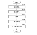
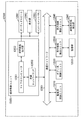
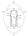
- FIG. 38 It is a figure which shows an example of the schematic structure of the image pickup system provided with the image pickup apparatus which concerns on the said Embodiment and the modification. It is a figure which shows an example of the imaging procedure in the imaging system of FIG. 38. It is a block diagram which shows an example of the schematic structure of a vehicle control system. It is explanatory drawing which shows an example of the installation position of the vehicle exterior information detection unit and the image pickup unit. It is a figure which shows an example of the schematic structure of the endoscopic surgery system. It is a block diagram which shows an example of the functional structure of a camera head and a CCU.
- Third Embodiment Example in which wiring is provided directly on the gate of the transfer transistor
- Fourth Embodiment Example in which the gate of the transfer transistor and the wiring are integrally formed
- Fifth Embodiment Example of providing wiring having a laminated structure between the first semiconductor substrate and the second semiconductor substrate and between the second semiconductor substrate and the third semiconductor substrate
- Modification example 6-1 Example of providing wiring having a laminated structure between the first semiconductor substrate and the second semiconductor substrate and between the second semiconductor substrate and the third semiconductor substrate
- Modification example 6-1 Example using Modification 1 (Example using vertical TG) 6-2.
- Deformation example 2 Example using Cu-Cu bonding at the outer edge of the panel
- Modification 3 Example in which FD is provided for each sensor pixel
- Modification 4 Example in which an offset is provided between the sensor pixel and the readout circuit 6-5.
- Modification 5 (Example in which a silicon substrate provided with a readout circuit has an island shape) 6-6.
- Modification 6 Example in which a silicon substrate provided with a readout circuit has an island shape
- Modification 7 Example in which the column signal processing circuit is composed of a general column ADC circuit
- Modification 8 Example in which the imaging device is configured by laminating three substrates
- Modification 9 Example in which logic circuits are provided on the first and second boards
- Modification 10 (Example in which a logic circuit is provided on a third substrate) 7.
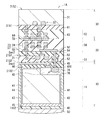
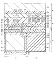
- FIG. 1 schematically shows an example of a cross-sectional configuration of a main part of a semiconductor device (semiconductor device 1) according to the first embodiment of the present disclosure in the vertical direction (Y-axis direction).
- the semiconductor device 1 is a semiconductor device having a three-dimensional structure in which a device layer A1 and a device layer A2 are laminated, and a semiconductor layer W1 and a metal layer W2 are formed on a wiring layer B between the device layer A1 and the device layer A2. It has a configuration in which a wiring W in which and is laminated is provided.
- This semiconductor device 1 can be applied to, for example, an imaging device having a three-dimensional structure. Therefore, the configuration of the image pickup apparatus 1A described later will be described. The detailed configuration of the image pickup apparatus 1A will be described later.
- the image pickup apparatus 1A includes a first substrate 10 having a sensor pixel 12 that performs photoelectric conversion on the semiconductor substrate 11, and a readout circuit 22 that outputs an image signal based on the charge output from the sensor pixel 12 on the semiconductor substrate 21.
- the second substrate 20 and the third substrate 30 having the logic circuit 32 (signal processing circuit) are laminated (see FIG. 7).
- the semiconductor substrate 11 corresponds to the device layer A1
- the semiconductor substrate 21 corresponds to the device layer A2.
- the semiconductor layer 49A and the metal layer extend between the semiconductor substrate 11 and the semiconductor substrate 21 in a direction parallel to the semiconductor substrate 11.
- a wiring 49 in which 49B is laminated is provided.
- the semiconductor layer 49A, the metal layer 49B, and the wiring 49 correspond to the semiconductor layer W1, the metal layer W2, and the wiring W, respectively.
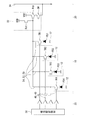
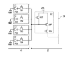
- FIG. 2 shows an example of the sensor pixel 12, the readout circuit 22, and the logic circuit 32 (vertical drive circuit 33).
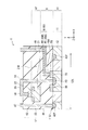
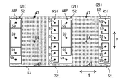
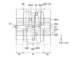
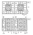
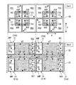
- FIG. 3A shows the layout in the device layer A1
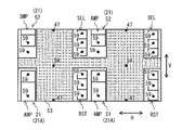
- FIG. 3B shows the layout in the device layer A2 and the wiring layer B.
- 3A and 3B illustrate the configuration of four 2x2 sensor pixels 12 sharing one floating diffusion FD.
- the unit area corresponding to the four 2 ⁇ 2 sensor pixels 12 sharing this one floating diffusion FD will be referred to as a unit area 12X for convenience.
- the cross section shown in FIG. 1 corresponds to the lines I-I and II-II shown in FIGS. 3A and 3B. However, it is assumed that the lines I-I and II-II are shown for convenience and do not completely coincide with FIG.
- the first substrate 10 has a plurality of sensor pixels 12 that perform photoelectric conversion on the semiconductor substrate 11.
- the semiconductor substrate 11 corresponds to a specific example of the "first semiconductor substrate” and the "first device layer” of the present disclosure.
- the plurality of sensor pixels 12 are provided in a matrix in the pixel region 13 of the first substrate 10.
- the first substrate 10 shares a floating diffusion FD that temporarily holds the electric charge output from the photodiode PD for each of the four sensor pixels 12.
- Each sensor pixel 12 has a component common to each other.
- the second substrate 20 has one readout circuit 22 for each of the four sensor pixels 12 on the semiconductor substrate 21 to output a pixel signal based on the charge output from the sensor pixel 12.
- the semiconductor substrate 21 corresponds to a specific example of the "second semiconductor substrate” and the “second device layer” of the present disclosure.
- the third substrate 30 has a logic circuit 32 for processing a pixel signal on the semiconductor substrate 31.
- the semiconductor substrate 31 corresponds to a specific example of the "third semiconductor substrate” of the present disclosure.
- the logic circuit 32 has, for example, a vertical drive circuit 33.
- Each sensor pixel 12 is, for example, a floating diffusion that temporarily holds the electric charge output from the photodiode PD, the transfer transistor TR electrically connected to the photodiode PD, and the electric charge output from the photodiode PD via the transfer transistor TR. It has an FD.
- the cathode of the photodiode PD is electrically connected to the source of the transfer transistor TR, and the anode of the photodiode PD is electrically connected to the reference potential line (eg, ground).
- the drain of the transfer transistor TR is electrically connected to the floating diffusion FD, and the gate of the transfer transistor TR is electrically connected to the vertical drive circuit 33 via, for example, the pixel drive line 23 described later.
- the floating diffusion FD shared by the four sensor pixels 12 is electrically connected to the input end of the common read circuit 22.
- the readout circuit 22 has, for example, a reset transistor RST, a selection transistor SEL, and an amplification transistor AMP.
- the source of the reset transistor RST (the input end of the read circuit 22) is electrically connected to the floating diffusion FD, and the drain of the reset transistor RST is electrically connected to the power line VDD and the drain of the amplification transistor AMP.
- the source of the amplification transistor AMP is electrically connected to the drain of the selection transistor SEL, and the gate of the amplification transistor AMP is electrically connected to the source of the reset transistor RST.
- the first substrate 10 has a photodiode PD and a transfer transistor TR for each sensor pixel 12, and a floating diffusion FD is shared for each of the four sensor pixels 12.
- the four transfer gates TG provided in each sensor pixel 12 in the unit area 12X are arranged so as to surround one floating diffusion FD.
- the reset transistor RST, the selection transistor SEL, and the amplification transistor AMP are arranged along a pair of opposite sides of the unit region 12X, respectively, as shown in FIG. 3B.
- the semiconductor device 1 has a configuration in which the first substrate 10 and the second substrate 20 are laminated in this order.
- the first substrate 10 is configured by laminating an insulating layer 46 as a part of the interlayer insulating film 51 on the surface (surface 11S1) of the semiconductor substrate 11.
- the semiconductor substrate 11 is made of a silicon substrate.
- the semiconductor substrate 11 has, for example, a p-well 42 composed of a p-type semiconductor region and a photodiode PD41 composed of a conductive (specifically n-type) semiconductor region different from the p-well 42. ing.
- the semiconductor substrate 11 has a floating diffusion FD in the p-well 42 as a conductive type (specifically, n-type) semiconductor region different from the p-well 42.
- the semiconductor substrate 11 has a contact diffusion layer 42P in the p-well 42, which is the same conductive type (specifically, p-type) as the p-well 42 and has a higher impurity concentration than the p-well 42. .. That is, the first substrate 10 has a transfer transistor TR, a floating diffusion FD, and a diffusion layer 42P for contact on a part of the surface 11S1 side (the side opposite to the light incident surface side, the second substrate 20 side) of the semiconductor substrate 11. It has a provided configuration.
- the second substrate 20 is configured by laminating an insulating layer 52 as a part of the interlayer insulating film 51 on the semiconductor substrate 21.
- the semiconductor substrate 21 is made of a silicon substrate.
- the second substrate 20 has one readout circuit 22 for every four sensor pixels 12.
- the second substrate 20 has a configuration in which a readout circuit 22 is provided on a part of the surface (surface 21S1) side of the semiconductor substrate 21.
- the second substrate 20 further has an insulating layer 53 as a part of the interlayer insulating film 51 in the same layer as the semiconductor substrate 21.
- the second substrate 20 has, for example, a connection portion 59 connected to a read circuit 22 (specifically, a reset transistor RST) in the insulating layer 52.
- the second substrate 20 further has, for example, a connection wiring 55 on the insulating layer 52.
- the connection wiring 55 connects the connection portion 59 and the through wiring 54 described later, whereby the floating diffusion FD and the read circuit 22 are electrically connected.
- the laminate composed of the first substrate 10 and the second substrate 20 has a through wiring 54 provided in the interlayer insulating film 51.
- the through wiring 54 corresponds to a specific example of the "first through wiring" of the present disclosure.
- the laminated body has one through wiring 54 for each sensor pixel 12.
- the through wiring 54 extends in the normal direction (Y-axis direction) of the semiconductor substrate 21, and is provided so as to penetrate the portion of the interlayer insulating film 51 including the insulating layer 53.
- the first substrate 10 and the second substrate 20 are electrically connected to each other by a through wiring 54.
- the through wiring 54 electrically connects the floating diffusion FD and the read circuit 22 together with the connection wiring 55 and the connection portion 59.
- the laminate composed of the first substrate 10 and the second substrate 20 further has through wirings 47 and 48 provided in the interlayer insulating film 51.
- the laminated body has, for example, one or more through wirings 47 and one through wiring 48 for each of the four sensor pixels 12.
- the through wirings 47 and 48 extend in the normal direction of the semiconductor substrate 21, respectively, and are provided so as to penetrate the portion of the interlayer insulating film 51 including the insulating layer 53.
- the first substrate 10 and the second substrate 20 are electrically connected to each other by through wirings 47 and 48.
- the through wiring 47 electrically connects the contact diffusion layer 42P of the semiconductor substrate 11 and the wiring (specifically, the vertical signal line 24) in the second substrate 20.
- one end of the through wiring 48 is provided between the semiconductor substrate 11 and the semiconductor substrate 21, and is connected to the wiring 49 extending in the direction parallel to the semiconductor substrate 11, and the other end is the second substrate. It is connected to the wiring inside 20 (specifically, the pixel drive line 23), and electrically connects the transfer gate TG of the transfer transistor TR and the vertical drive circuit 33.
- the through wiring 48 is formed in, for example, the peripheral region 14 shown in FIG. 27, which will be described later.
- the laminate composed of the first substrate 10 and the second substrate 20 further has a wiring 49 in the interlayer insulating film 51.
- the wiring 49 corresponds to the wiring W and also corresponds to a specific example of the “wiring” of the present disclosure.
- the wiring 49 is provided in the insulating layer 46 between the semiconductor substrate 11 constituting the first substrate 10 and the semiconductor substrate 21 constituting the second substrate 20.
- the wiring 49 together with the via 49V and the through wiring 48, electrically connects the transfer gate TG of the transfer transistor TR and the vertical drive circuit 33.
- One wiring 49 is provided for each of the four sensor pixels 12 arranged in the unit area 12X. That is, in the unit region 12X, as shown in FIG.
- each wiring 49X1, 49X2, 49X3, 49X4 is arranged in a band shape, for example, between the reset transistor RST and the selection transistor SEL and the amplification transistor AMP. Have been placed.
- Each wiring 49X1, 49X2, 49X3, 49X4 shifts vias 49V1, 49V2, 49V3, 49V4 connecting the transfer gate TG of each transfer transistor TR1, TR2, TR3, TR4 and each wiring 49X1, 49X2, 49X3, 49X4. By providing them, they can be formed independently of each other.
- the wiring 49 has a laminated structure in which the semiconductor layer 49A and the metal layer 49B are laminated in order from the semiconductor substrate 11 side.
- the material of the semiconductor layer 49A include Si, Ge, SiGe, SiC, ZnSe, GaAs, GaP, InP, InN, GaN, InGaN, GaAlAs, IGaAs, GaInNAs, InGaAlP, ZnO, IGZO, MoS 2 , MoSe 2 , Examples include polymers or amorphous or single crystals of MoTe 2 , WS 2 , WSe 2 , WTe 2 , ZrS 2 , ZrSe 2 , ZrTe 2 , HfS 2 , HfSe 2 , HfTe 2 , graphene, phospherene and carbon nanotubes.
- the material of the metal layer 49B is, for example, one or more of tungsten (W), aluminum (Al), cobalt (Co), nickel (Ni) and platinum (Pt), or any of the above metals. Examples thereof include a compound (0045) with a heel silicon (Si).
- the wiring 49 and the transfer gate TG are connected via the via 49V. Examples of the material of the via 49V include the semiconductors mentioned in the semiconductor layer 49A.
- the wiring 49 and the vertical drive circuit 33 are connected via a through wiring 48. Examples of the material of the through wiring 48 include the metals mentioned in the metal layer 49B.
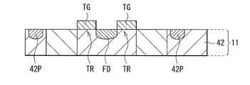
- the p-well 42, the element separation portion 43, and the p-well layer 44 are formed on the semiconductor substrate 11.
- the photodiode PD41, the transfer transistor TR, and the floating diffusion FD are formed on the semiconductor substrate 11 (FIG. 4A).
- the sensor pixel 12 is formed on the semiconductor substrate 11.
- the insulating layer 46A is formed on the semiconductor substrate 11.
- the insulating layer 46B is formed on the insulating layer 46A and the semiconductor layer 49A (FIG. 4C). In this way, the first substrate 10 is formed.
- an opening 21H penetrating the semiconductor substrate 21 is formed, and the semiconductor substrate 21 is separated into a plurality of blocks 21A.
- the insulating layer 53 is formed so as to embed the opening 21H.
- a readout circuit 22 including an amplification transistor AMP and the like is formed in each block 21A of the semiconductor substrate 21 (FIG. 4D).
- an opening H1 penetrating the insulating layers 52A, 53, and 46 is formed at a position corresponding to the semiconductor layer 49A (FIG. 4E).
- the metal layer 49B is formed on the semiconductor layer 49A (FIG. 4F).
- the metal layer 49B can be formed using silicide. For example, cobalt (Co) or nickel (Ni) is sputtered onto the semiconductor layer 49A and then annealed. Then, the unreacted portion is removed and the annealing treatment is performed again. As a result, the metal layer 49B is formed on the semiconductor layer 49A.
- the metal layer 49B may be formed by using selective CVD.
- the metal layer 49B made of a W film can be selectively formed on the semiconductor layer 49A by selective CVD using tungsten fluoride (WF 6 ) and silane (SiH 4 ).
- the insulating layer 52 is formed by forming an insulating layer on the insulating layer 52A and the metal layer 49B so as to embed the opening H1.
- the interlayer insulating film 51 composed of the insulating layers 46, 52, and 53 is formed (FIG. 4G).
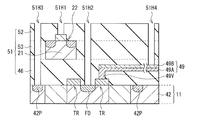
- through holes 51H1, 51H2, 51H3, 51H4 are formed in the interlayer insulating film 51 (FIG. 4H).
- a through hole 51H1 penetrating the insulating layer 52 is formed in the interlayer insulating film 51 at a position facing the readout circuit 22.
- a through hole 51H2 penetrating the interlayer insulating film 51 is formed at a portion of the interlayer insulating film 51 facing the floating diffusion FD. Further, a through hole 51H3 penetrating the interlayer insulating film 51 is formed at a portion of the interlayer insulating film 51 facing the contact diffusion layer 42P. Furthermore, a through hole 51H4 penetrating the interlayer insulating film 51 is formed at a position facing the wiring 49.
- the through wiring 54 is formed in the through hole 51H1 and the connection portion 59 is formed in the through hole 51H2. Further, a through wiring 47 is formed in the through hole 51H3, and a through wiring 48 is formed in the through hole 51H4. Subsequently, a connection wiring 55 that electrically connects the through wiring 54 and the connection portion 59 to each other is formed on the insulating layer 52 (FIG. 4I). In this way, the second substrate 20 is formed, and the semiconductor device 1 shown in FIG. 1 is manufactured.
- FIG. 5 schematically shows a cross-sectional configuration in the vertical direction (Y-axis direction) of the semiconductor device 100 having a general three-dimensional structure corresponding to the semiconductor device 1 shown in FIG.
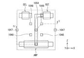
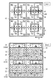
- FIG. 6A shows the layout in the device layer A100
- FIG. 6B shows the layout in the device layer A200.
- the cross section shown in FIG. 5 corresponds to the lines III-III and IV-IV shown in FIGS. 6A and 6B. However, it is assumed that the lines III-III and IV-IV are shown for convenience and do not completely coincide with FIG.
- a transfer transistor is formed around a through wiring 1054 that electrically connects the floating diffusion FD and the read circuit 1022.
- a plurality of (four in the semiconductor device 100) through wires 1048 that electrically connect the transfer gate TG of the TR and the vertical drive line (not shown) are formed so as to run in parallel. Therefore, the capacitance (parasitic capacitance) between the through wiring 1054 and the through wiring 1048 becomes large.
- the semiconductor layer W1 and the metal layer W2 are laminated in the wiring layer B between the device layer A1 and the device layer A2 in a direction parallel to the device layer A1.
- the wiring W was formed.
- the total number of through wirings extending in the stacking direction of the device layer A1 and the device layer A2 is reduced. This makes it possible to reduce the parasitic capacitance between the through wirings.
- FIG. 7 shows an example of the vertical cross-sectional configuration of the image pickup apparatus (imaging apparatus 1A) according to the first embodiment of the present disclosure.
- FIG. 8 shows an example of the schematic configuration of the image pickup apparatus 1A shown in FIG. 7.
- three substrates first substrate 10, second substrate 20 and third substrate 30 are laminated in this order.
- the first substrate 10 has a plurality of sensor pixels 12 that perform photoelectric conversion on the semiconductor substrate 11.
- the plurality of sensor pixels 12 are provided in a matrix in the pixel region 13 of the first substrate 10.
- the first substrate 10 shares a floating diffusion FD that temporarily holds the electric charge output from the photodiode PD for each of the four sensor pixels 12.
- the second substrate 20 has one readout circuit 22 for each of the four sensor pixels 12 on the semiconductor substrate 21 to output a pixel signal based on the charge output from the sensor pixel 12.
- the second substrate 20 has a plurality of pixel drive lines 23 extending in the row direction and a plurality of vertical signal lines 24 extending in the column direction.
- the plurality of pixel drive lines 23 may be provided, for example, on the first substrate 10 side (for example, in the interlayer insulating film 51 between the semiconductor substrate 11 and the semiconductor substrate 21).
- the third substrate 30 has a logic circuit 32 for processing a pixel signal on the semiconductor substrate 31.
- the semiconductor substrate 31 corresponds to a specific example of the "third semiconductor substrate" of the present disclosure.
- the logic circuit 32 includes, for example, a vertical drive circuit 33, a column signal processing circuit 34, a horizontal drive circuit 35, and a system control circuit 36.
- the logic circuit 32 (specifically, the horizontal drive circuit 35) outputs the output voltage Vout for each sensor pixel 12 to the outside.
- a low resistance region made of silicide formed by using a salicide (Self Aligned Silicide) process such as CoSi 2 or NiSi is formed on the surface of the impurity diffusion region in contact with the source electrode and the drain electrode. You may.
- the vertical drive circuit 33 selects a plurality of sensor pixels 12 in order in line units.
- the column signal processing circuit 34 performs, for example, Correlated Double Sampling (CDS) processing on the pixel signals output from each sensor pixel 12 in the row selected by the vertical drive circuit 33.
- CDS Correlated Double Sampling
- the column signal processing circuit 34 extracts the signal level of the pixel signal by performing CDS processing, for example, and holds pixel data according to the amount of light received by each sensor pixel 12.
- the horizontal drive circuit 35 sequentially outputs the pixel data held in the column signal processing circuit 34 to the outside, for example.
- the system control circuit 36 controls the drive of each block (vertical drive circuit 33, column signal processing circuit 34, and horizontal drive circuit 35) in the logic circuit 32, for example.
- FIG. 9 shows an example of the sensor pixel 12 and the readout circuit 22.
- FIG. 3A a case where the four sensor pixels 12 share one floating diffusion FD and one readout circuit 22 will be described.
- “sharing” means that the outputs of the four sensor pixels 12 are input to the common floating diffusion FD and the read circuit 22.
- Each sensor pixel 12 has a component common to each other.
- an identification number (1, 2, 3, 4) is added to the end of the code of the component of each sensor pixel 12 in order to distinguish the components of each sensor pixel 12 from each other.
- an identification number is given at the end of the code of the component of each sensor pixel 12, but the components of each sensor pixel 12 are distinguished from each other. If it is not necessary to do so, the identification number at the end of the code of the component of each sensor pixel 12 shall be omitted.
- Each sensor pixel 12 is, for example, a floating diffusion that temporarily holds the electric charge output from the photodiode PD, the transfer transistor TR electrically connected to the photodiode PD, and the electric charge output from the photodiode PD via the transfer transistor TR. It has an FD.
- the photodiode PD corresponds to a specific example of the "photoelectric conversion element" of the present disclosure.
- the photodiode PD performs photoelectric conversion to generate an electric charge according to the amount of received light.
- the cathode of the photodiode PD is electrically connected to the source of the transfer transistor TR, and the anode of the photodiode PD is electrically connected to the reference potential line (eg, ground).
- the drain of the transfer transistor TR is electrically connected to the floating diffusion FD, and the gate of the transfer transistor TR is electrically connected to the pixel drive line 23.
- the transfer transistor TR is, for example, a CMOS (Complementary Metal Oxide Semiconductor) transistor.
- the floating diffusion FD shared by the four sensor pixels 12 is electrically connected to the input terminal of the common read circuit 22.
- the readout circuit 22 has, for example, a reset transistor RST, a selection transistor SEL, and an amplification transistor AMP.
- the selection transistor SEL may be omitted if necessary.
- the source of the reset transistor RST (the input end of the read circuit 22) is electrically connected to the floating diffusion FD, and the drain of the reset transistor RST is electrically connected to the power line VDD and the drain of the amplification transistor AMP.
- the gate of the reset transistor RST is electrically connected to the pixel drive line 23.
- the source of the amplification transistor AMP is electrically connected to the drain of the selection transistor SEL, and the gate of the amplification transistor AMP is electrically connected to the source of the reset transistor RST.
- the source of the selection transistor SEL (the output end of the readout circuit 22) is electrically connected to the vertical signal line 24, and the gate of the selection transistor SEL is electrically connected to the pixel drive line 23.
- the transfer transistor TR transfers the electric charge of the photodiode PD to the floating diffusion FD when the transfer transistor TR is turned on.
- the gate (transfer gate TG) of the transfer transistor TR has, for example, a planar transfer gate TG as shown in FIG. 7, and is formed on the surface of the semiconductor substrate 11.
- the reset transistor RST resets the potential of the floating diffusion FD to a predetermined potential. When the reset transistor RST is turned on, the potential of the floating diffusion FD is reset to the potential of the power supply line VDD.
- the selection transistor SEL controls the output timing of the pixel signal from the readout circuit 22.
- the amplification transistor AMP generates a voltage signal as a pixel signal according to the level of the electric charge held in the floating diffusion FD.
- the amplification transistor AMP constitutes a source follower type amplifier, and outputs a pixel signal having a voltage corresponding to the level of electric charge generated by the photodiode PD.
- the selection transistor SEL When the selection transistor SEL is turned on, the amplification transistor AMP amplifies the potential of the floating diffusion FD and outputs a voltage corresponding to the potential to the column signal processing circuit 34 via the vertical signal line 24.
- the reset transistor RST, amplification transistor AMP and selection transistor SEL are, for example, CMOS transistors.
- the selection transistor SEL may be provided between the power supply line VDD and the amplification transistor AMP.
- the drain of the reset transistor RST is electrically connected to the drain of the power supply line VDD and the selection transistor SEL.
- the source of the selection transistor SEL is electrically connected to the drain of the amplification transistor AMP, and the gate of the selection transistor SEL is electrically connected to the pixel drive line 23.
- the source of the amplification transistor AMP (the output end of the readout circuit 22) is electrically connected to the vertical signal line 24, and the gate of the amplification transistor AMP is electrically connected to the source of the reset transistor RST.
- the FD transfer transistor FDG may be provided between the source of the reset transistor RST and the gate of the amplification transistor AMP.
- the FD transfer transistor FDG is used when switching the conversion efficiency.
- the FD transfer transistor FDG when the FD transfer transistor FDG is turned on, the gate capacitance for the FD transfer transistor FDG increases, so that the overall FD capacitance C increases. On the other hand, when the FD transfer transistor FDG is turned off, the overall FD capacitance C becomes smaller. By switching the FD transfer transistor FDG on and off in this way, the FD capacitance C can be made variable and the conversion efficiency can be switched.
- FIG. 13 shows an example of a connection mode between the plurality of readout circuits 22 and the plurality of vertical signal lines 24.
- the plurality of read circuits 22 are arranged side by side in the extending direction (for example, the column direction) of the vertical signal lines 24, even if one of the plurality of vertical signal lines 24 is assigned to each read circuit 22. Good.
- the four vertical signal lines 24 are the read circuits 22. It may be assigned one for each.
- an identification number (1, 2, 3, 4) is added to the end of the code of each vertical signal line 24 in order to distinguish each vertical signal line 24.
- the image pickup apparatus 1A has a configuration in which the first substrate 10, the second substrate 20, and the third substrate 30 are laminated in this order, and further, on the back surface (light incident surface) side of the first substrate 10. , A color filter 40 and a light receiving lens 50.
- One color filter 40 and one light receiving lens 50 are provided for each sensor pixel 12, for example. That is, the image pickup device 1A is a back-illuminated image pickup device.
- the first substrate 10 is configured by laminating an insulating layer 46 on the surface (surface 11S1) of the semiconductor substrate 11.
- the first substrate 10 has an insulating layer 46 as a part of the interlayer insulating film 51.
- the insulating layer 46 is provided between the semiconductor substrate 11 and the semiconductor substrate 21 described later.
- the semiconductor substrate 11 is made of a silicon substrate.
- the semiconductor substrate 11 has, for example, a p-well 42 in a part of the surface or in the vicinity thereof, and in a region other than the p-well 42 (a region deeper than the p-well 42), a conductive type PD 41 different from the p-well 42. have.
- the p-well 42 is composed of a p-type semiconductor region.
- the PD 41 is composed of a conductive type (specifically, n type) semiconductor region different from the p-well 42.
- the semiconductor substrate 11 has a floating diffusion FD in the p-well 42 as a conductive type (specifically, n-type) semiconductor region different from the p-well 42.
- the first substrate 10 has a photodiode PD and a transfer transistor TR for each sensor pixel 12, and shares a floating diffusion FD for each of the four sensor pixels 12.
- the first substrate 10 has a configuration in which a transfer transistor TR and a floating diffusion FD are provided on a part of the surface 11S1 side (the side opposite to the light incident surface side, the second substrate 20 side) of the semiconductor substrate 11. ..
- the first substrate 10 has an element separation unit 43 that separates each sensor pixel 12.
- the element separation unit 43 does not completely surround the sensor pixel 12 when viewed from the normal direction of the semiconductor substrate 11 (direction perpendicular to the surface of the semiconductor substrate 11), and the floating diffusion FD (through wiring 54). There is a gap (unformed region) in the vicinity of the above and in the vicinity of the through wiring 47. The gap allows the four sensor pixels 12 to share one through wiring 54 and the four sensor pixels 12A to share one through wiring 47.
- the element separation unit 43 is made of, for example, silicon oxide. The element separation unit 43 penetrates, for example, the semiconductor substrate 11.
- the first substrate 10 further has, for example, a p-well layer 44 which is a side surface of the element separating portion 43 and is in contact with the surface on the photodiode PD side.
- the p-well layer 44 is composed of a conductive type (specifically, p-type) semiconductor region different from the photodiode PD.
- the first substrate 10 further has, for example, a fixed charge film 45 in contact with the back surface (surface 11S2, other surface) of the semiconductor substrate 11.
- the fixed charge film 45 is negatively charged in order to suppress the generation of dark current due to the interface state on the light receiving surface side of the semiconductor substrate 11.
- the fixed charge film 45 is formed of, for example, an insulating film having a negative fixed charge.
- the material of such an insulating film examples include hafnium oxide, zircon oxide, aluminum oxide, titanium oxide and tantalum oxide.
- the electric field induced by the fixed charge film 45 forms a hole storage layer at the interface on the light receiving surface side of the semiconductor substrate 11.
- the hole accumulation layer suppresses the generation of electrons from the interface.
- the color filter 40 is provided on the back surface side of the semiconductor substrate 11.
- the color filter 40 is provided, for example, in contact with the fixed charge film 45, and is provided at a position facing the sensor pixel 12 via the fixed charge film 45.
- the light receiving lens 50 is provided, for example, in contact with the color filter 40, and is provided at a position facing the sensor pixel 12 via the color filter 40 and the fixed charge film 45.
- the second substrate 20 is configured by laminating an insulating layer 52 on the semiconductor substrate 21.
- the second substrate 20 has an insulating layer 52 as a part of the interlayer insulating film 51.
- the insulating layer 52 is provided between the semiconductor substrate 21 and the semiconductor substrate 31.
- the semiconductor substrate 21 is made of a silicon substrate.
- the second substrate 20 has one readout circuit 22 for every four sensor pixels 12.
- the second substrate 20 has a configuration in which a readout circuit 22 is provided on a part of the surface side of the semiconductor substrate 21 (the surface 21S1 facing the third substrate 30, one surface).
- the second substrate 20 is attached to the first substrate 10 with the back surface (surface 21S2, other surface) of the semiconductor substrate 21 facing the front surface (surface 11S1) of the semiconductor substrate 11.
- the second substrate 20 is attached to the first substrate 10 face-to-back.
- the second substrate 20 further has an insulating layer 53 in the same layer as the semiconductor substrate 21.
- the second substrate 20 has an insulating layer 53 as a part of the interlayer insulating film 51.
- the insulating layer 53 is formed in the opening 21H penetrating the semiconductor substrate 21, and is provided so as to cover the side surfaces of the penetrating wirings 47, 48, 54 described above.
- the second substrate 20 has, for example, a plurality of connecting portions 59 electrically connected to the readout circuit 22 and the semiconductor substrate 21 in the insulating layer 52.
- the second substrate 20 further has, for example, a wiring layer 56 on the insulating layer 52.
- the wiring layer 56 has, for example, an insulating layer 57, a plurality of pixel drive lines 23 provided in the insulating layer 57, and a plurality of vertical signal lines 24.
- the wiring layer 56 further has, for example, a plurality of connection wirings 55 in the insulating layer 57, one for each of the four sensor pixels 12.
- the connection wiring 55 electrically connects each through wiring 54 electrically connected to the floating diffusion FD included in the four sensor pixels 12 sharing the read circuit 22 to each other.
- the wiring layer 56 further has, for example, a plurality of pad electrodes 58 in the insulating layer 57.
- Each pad electrode 58 is made of, for example, a metal such as Cu (copper) or Al (aluminum).
- Each pad electrode 58 is exposed on the surface of the wiring layer 56.
- Each pad electrode 58 is used for electrical connection between the second substrate 20 and the third substrate 30 and for bonding the second substrate 20 and the third substrate 30.
- the plurality of pad electrodes 58 are provided, for example, one for each of the pixel drive line 23 and the vertical signal line 24.
- the total number of pad electrodes 58 (or the total number of joints between the pad electrodes 58 and the pad electrodes 64 (described later) is smaller than the total number of sensor pixels 12 included in the first substrate 10.
- the third substrate 30 is configured by, for example, laminating an interlayer insulating film 61 on a semiconductor substrate 31. As will be described later, the third substrate 30 is attached to the second substrate 20 with the surfaces on the front side facing each other. Therefore, when explaining the configuration inside the third substrate 30, the upper and lower parts will be described. , It is the opposite of the vertical direction in the drawing.
- the semiconductor substrate 31 is made of a silicon substrate.
- the third substrate 30 has a configuration in which a logic circuit 32 is provided on a part of the surface (surface 31S1) side of the semiconductor substrate 31.
- the third substrate 30 further has, for example, a wiring layer 62 on the interlayer insulating film 61.
- the wiring layer 62 has, for example, an insulating layer 63 and a plurality of pad electrodes 64 provided in the insulating layer 63.
- the plurality of pad electrodes 64 are electrically connected to the logic circuit 32.
- Each pad electrode 64 is made of, for example, Cu (copper).
- Each pad electrode 64 is exposed on the surface of the wiring layer 62.
- Each pad electrode 64 is used for electrical connection between the second substrate 20 and the third substrate 30 and for bonding the second substrate 20 and the third substrate 30. Further, the number of pad electrodes 64 does not necessarily have to be plurality, and even one pad electrode 64 can be electrically connected to the logic circuit 32.
- the second substrate 20 and the third substrate 30 are electrically connected to each other by joining the pad electrodes 58 and 64 to each other.
- the third substrate 30 is attached to the second substrate 20 with the surface (surface 31S1) of the semiconductor substrate 31 facing the surface (surface 21S1) side of the semiconductor substrate 21. That is, the third substrate 30 is attached to the second substrate 20 face-to-face.
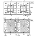
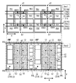
- FIG. 14 shows an example of the cross-sectional configuration of the image pickup apparatus 1A in the horizontal direction.
- the upper view of FIG. 14 is a diagram showing an example of the cross-sectional configuration of the cross section Sec1 of FIG. 7, and the lower view of FIG. 14 is a diagram showing an example of the cross-sectional configuration of the cross section Sec2 of FIG. ..
- FIG. 14 illustrates a configuration in which two sets of four 2 ⁇ 2 sensor pixels 12 are arranged in the second direction H.
- a diagram showing an example of the surface configuration of the semiconductor substrate 11 is superimposed on a diagram showing an example of the cross-sectional configuration of the cross section Sec1 of FIG. 7, and the insulating layer 46 is omitted.
- a diagram showing an example of the surface configuration of the semiconductor substrate 21 is superimposed on a diagram showing an example of the cross-sectional configuration in the cross-sectional section Sec2 of FIG. 7.
- the four sensor pixels 12 corresponding to the region will be referred to as four sensor pixels 12A for convenience.
- the first substrate 10 shares the through wiring 47 for each of the four sensor pixels 12A.
- the first direction V is parallel to one of the two arrangement directions (for example, the row direction and the column direction) of the plurality of sensor pixels 12 arranged in a matrix (for example, the column direction).
- the four transfer gates TGs are arranged so as to surround one floating diffusion FD, for example, the four transfer gates TGs form a ring shape. It has a shape of.
- the insulating layer 53 is composed of a plurality of blocks extending in the first direction V.
- the semiconductor substrate 21 is composed of a plurality of island-shaped blocks 21A extending in the first direction V and arranged side by side in the second direction H orthogonal to the first direction V via an insulating layer 53. ..
- Each block 21A is provided with, for example, a plurality of sets of reset transistors RST, amplification transistor AMP, and selection transistor SEL.
- One read-out circuit 22 shared by the four sensor pixels 12 is composed of, for example, a reset transistor RST, an amplification transistor AMP, and a selection transistor SEL in a region facing the four sensor pixels 12.
- One readout circuit 22 shared by the four sensor pixels 12 includes, for example, an amplification transistor AMP in the block 21A to the left of the insulating layer 53 and a reset transistor RST in the block 21A to the right of the insulating layer 53. It is composed of a transistor SEL.
- FIG. 15 shows another example of the horizontal cross-sectional configuration of the image pickup apparatus 1A.
- the first substrate 10 has a photodiode PD and a transfer transistor TR for each sensor pixel 12, and shares a floating diffusion FD for each of the four sensor pixels 12. Further, the first substrate 10 has an element separation unit 43 that separates the photodiode PD and the transfer transistor TR for each sensor pixel 12.
- the semiconductor substrate 21 provided with the reset transistor RST, the amplification transistor AMP, and the selection transistor SEL is formed into an island shape for each of the four sensor pixels sharing one floating diffusion FD. It is different from the cross section Sec2 of.
- FIG. 16 shows another example of the horizontal cross-sectional configuration of the image pickup apparatus 1A.
- the first substrate 10 has a photodiode PD and a transfer transistor TR for each sensor pixel 12, and shares a floating diffusion FD for each of the four sensor pixels 12. Further, the first substrate 10 has an element separation unit 43 that separates the photodiode PD and the transfer transistor TR for each sensor pixel 12.
- the semiconductor substrate 21 having an island shape for each of the four sensor pixels sharing one floating diffusion FD in FIG. 15 is arranged so as to be offset by one sensor pixel in the first direction V.
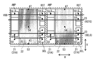
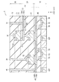
- FIG. 17, FIG. 18, FIG. 19 and FIG. 20 show an example of the wiring layout of the image pickup apparatus 1A in the horizontal plane. 17 to 20 illustrate a case where one readout circuit 22 shared by the four sensor pixels 12 is provided in a region facing the four sensor pixels 12.
- the wirings shown in FIGS. 17 to 20 are provided in different layers of the wiring layer 56, for example.
- the through wiring 54 is electrically connected to the connection wiring 55, for example, as shown in FIG. Further, as shown in FIG. 17, the through wiring 54 further includes the gate of the amplification transistor AMP included in the left adjacent block 21A of the insulating layer 53 and the insulating layer 53 via the connecting wiring 55 and the connecting portion 59. It is electrically connected to the gate of the reset transistor RST included in the right adjacent block 21A.
- the power supply line VDD is arranged at a position facing each read circuit 22 arranged side by side in the second direction H.
- the power line VDD is electrically connected to the drain of the amplification transistor AMP and the drain of the reset transistor RST of each readout circuit 22 arranged side by side in the second direction H via the connection portion 59. Is connected.
- the two pixel drive lines 23 are arranged at positions facing each of the read-out circuits 22 arranged side by side in the second direction H.
- One pixel drive line 23 (second control line) is electrically connected to the gate of the reset transistor RST of each read circuit 22 arranged side by side in the second direction H, for example, as shown in FIG. Wiring RSTG.
- the other pixel drive line 23 (third control line) is electrically connected to the gate of the selection transistor SEL of each readout circuit 22 arranged side by side in the second direction H, for example, as shown in FIG. Wiring SELG.
- the source of the amplification transistor AMP and the drain of the selection transistor SEL are electrically connected to each other via the wiring 25, for example, as shown in FIG.
- the two power supply lines VSS are arranged at positions facing each of the read-out circuits 22 arranged side by side in the second direction H, for example, as shown in the cross section Sec2 of FIG.
- Each power line VSS is electrically connected to a plurality of through wirings 47 at a position facing each sensor pixel 12 arranged side by side in the second direction H, for example, as shown in the cross section Sec2 of FIG. ing.
- the four pixel drive lines 23 (wiring 49) are arranged at positions facing each of the read-out circuits 22 arranged side by side in the second direction H, for example, as shown in the cross section Sec1 of FIG.
- Each of the four pixel drive lines 23 is, for example, a through wiring of one of the four sensor pixels 12 corresponding to each read circuit 22 arranged side by side in the second direction H. It is a wiring TRG electrically connected to 48. That is, the four pixel drive lines 23 (wiring 49, first control line) are electrically connected to the gate (transfer gate TG) of the transfer transistor TR of each sensor pixel 12 arranged side by side in the second direction H. Has been done. In the cross section Sec1 of FIG. 19, an identifier (1, 2, 3, 4) is added to the end of each wiring TRG in order to distinguish each wiring TRG.
- the vertical signal line 24 is arranged at a position facing each read-out circuit 22 arranged side by side in the first direction V.
- the vertical signal line 24 (output line) is electrically connected to the output end (source of the amplification transistor AMP) of each read circuit 22 arranged side by side in the first direction V. ing.
- the imaging device 1A of the present embodiment can be manufactured as follows, for example, following the manufacturing process of the semiconductor device 1 described with reference to FIGS. 4A to 4I.
- the surface of the semiconductor substrate 21 is directed to the surface side of the semiconductor substrate 31, and the third substrate 30 on which the logic circuit 32 and the wiring layer 62 are formed is formed.
- the pad electrode 58 of the second substrate 20 and the pad electrode 64 of the third substrate 30 are joined to each other to electrically connect the second substrate 20 and the third substrate 30 to each other. In this way, the image pickup apparatus 1A shown in FIG. 7 is manufactured.
- a conventional MOS process is used in forming an upper layer device in which a readout circuit or the like is formed.
- the conventional MOS process there is a high temperature process of 1000 ° C. or higher, so wiring is performed after the upper layer device is formed. For this reason, in an imaging device having a three-dimensional structure, wiring is likely to be redundant.
- the transfer gate TG of the transfer transistor TR and the second substrate (device layer A200) are provided around the through wiring 1054 extending in the normal direction of the semiconductor substrate 1011.
- a plurality of through wires 1048 that electrically connect to a pixel drive line (not shown) are formed so as to run in parallel, and a capacitance (parasitic capacitance) between the through wires 1054 and the through wires 1048. Becomes larger. As described above, in an imaging device having a three-dimensional structure, the parasitic capacitance tends to increase due to fringing or the like.
- the wiring can be routed under the upper layer device, so that the parasitic capacitance can be minimized, but the quality of the upper layer device deteriorates. Specifically, the noise characteristics and the like in the read circuit deteriorate.
- the direction parallel to the semiconductor substrate 11 is contained in the insulating layer 46 between the semiconductor substrate 11 constituting the first substrate 10 and the semiconductor substrate 21 constituting the second substrate 20.
- the semiconductor layer 49A and the metal layer 49B are laminated to form a wiring 49.
- the parallel running distance of the through wiring extending in the stacking direction of the first substrate 10 and the second substrate 20 is reduced.
- the through wiring 1054 that electrically connects the floating diffusion FD and the read circuit 1022 shown in FIG. 5, and the gate (TG) of the transfer transistor TR and the vertical drive circuit 33 are electrically connected. As shown in FIG.
- the parallel running distance with the penetrating wiring 1048 is reduced to the via 49V connecting the gate (TG) of the transfer transistor TR and the wiring 49.
- the total number of through wirings extending in the stacking direction of the first substrate 10 and the second substrate 20 is reduced.
- the first substrate 10 having the sensor pixel 12 that performs photoelectric conversion the second substrate 20 having the readout circuit 22 that outputs the image signal based on the charge output from the sensor pixel 12, and the third substrate having the logic circuit 32.
- the image pickup apparatus 1A having a three-dimensional structure in which 30s are stacked it is possible to reduce the parasitic capacitance.
- the wiring 49 since the wiring 49 has a laminated structure of the semiconductor layer 49A and the metal layer 49B, it is possible to reduce the resistance of the wiring 49 as compared with the case where the wiring 49 is formed only by the semiconductor layer 49A. .. That is, it is possible to form low resistance wiring between the semiconductor substrate 11 that constitutes the first substrate 10 and the semiconductor substrate 21 that constitutes the second substrate 20.
- FIG. 21 schematically shows a cross-sectional configuration in the vertical direction of the semiconductor device (semiconductor device 2) according to the second embodiment of the present disclosure.
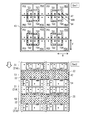
- FIG. 22A shows the layout in the device layer A1
- FIG. 22B shows the layout in the device layer A2 and the wiring layer B.
- the cross section shown in FIG. 21 corresponds to the VV line and the VI-VI line shown in FIGS. 22A and 22B.
- the semiconductor device 2 is formed on the device layer A1 (semiconductor substrate 11), the first substrate 10 having the sensor pixel 12 for photoelectric conversion, and the device layer A2 (semiconductor substrate 21).
- a laminated body in which a second substrate 20 having a readout circuit 22 for outputting an image signal based on the charge output from the sensor pixel 12 is laminated.
- the reset transistor RST, the selection transistor SEL, and the amplification transistor AMP are arranged along a pair of opposite sides of the unit region 12X, and a wiring 49 is formed between them.
- the reset transistor RST, the selection transistor SEL, and the amplification transistor AMP may be arranged so as to project to the center of the unit region 12X as shown in FIG. 22B.
- the four wirings 49X1, 49X2, 49X3, 49X4 arranged in a strip shape in the unit region 12X have a single layer structure of the semiconductor layer 49A in the region R1 having the semiconductor substrate 21 above, as shown in FIG.
- the semiconductor layer 49A and the metal layer 49B are laminated as in the first embodiment.
- the region R2 where the semiconductor substrate 21 is not above this corresponds to the “laminated region” of the present disclosure.
- the semiconductor is located in the region R2 where the reset transistor RST, the selection transistor SEL and the amplification transistor AMP are not arranged.
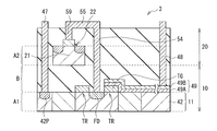
- FIG. 23 schematically shows a cross-sectional configuration in the vertical direction of the semiconductor device (semiconductor device 3) according to the third embodiment of the present disclosure.
- the semiconductor device 3 has a device layer A1 (semiconductor substrate 11), a first substrate 10 having sensor pixels 12 for photoelectric conversion, and a device layer A2 (semiconductor substrate 21).
- the wiring 49 is directly formed on the transfer gate TG of the transfer transistor TR without using the via 49V.
- FIG. 24 schematically shows a cross-sectional configuration in the vertical direction of a main part of the semiconductor device (semiconductor device 4) according to the fourth embodiment of the present disclosure. Similar to the first embodiment, the semiconductor device 4 is formed on the device layer A1 (semiconductor substrate 11), the first substrate 10 having the sensor pixels 12 for photoelectric conversion, and the device layer A2 (semiconductor substrate 21). , A laminated body in which a second substrate 20 having a readout circuit 22 for outputting an image signal based on the charge output from the sensor pixel 12 is laminated.
- the image pickup apparatus 1A of the present embodiment uses the transfer gate TG of the transfer transistor TR as the wiring 49.
- the transfer gate TG that also serves as the wiring 49 is formed by using a semiconductor material such as polysilicon (semiconductor layer 49A), and when there is no semiconductor substrate 21 above, as shown in FIG. 24. , Has a laminated structure in which a semiconductor layer 49A and a metal layer 49B are laminated.
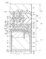
- FIG. 25 schematically shows a cross-sectional configuration in the vertical direction of a main part of the semiconductor device (semiconductor device 5) according to the fifth embodiment of the present disclosure. Similar to the image pickup device 1A of the first embodiment, the semiconductor device 5 outputs the first substrate 10 having the sensor pixel 12 that performs photoelectric conversion on the semiconductor substrate 11 and the sensor pixel 12 on the semiconductor substrate 21.
- This is an image pickup apparatus having a three-dimensional structure in which a second substrate 20 having a readout circuit 22 for outputting an image signal based on the charged charge and a third substrate 30 having a logic circuit 32 are laminated.
- the semiconductor substrate 21 and the semiconductor substrate 31 extend between the semiconductor substrate 21 constituting the second substrate 20 and the semiconductor substrate 31 constituting the third substrate 30.
- the wiring 73 having the region R2 in which the semiconductor layer 72A and the metal layer 72B are laminated is formed.
- the semiconductor substrate 31 and the semiconductor substrate 31 are provided in the same layer as the semiconductor substrate 31 as the third substrate 30 on the second substrate 20, and the insulating layer 71 and the semiconductor substrate 31 and as a part of the interlayer insulating film 51 are provided. It is provided on the insulating layer 71 and has an insulating layer 72 as a part of the interlayer insulating film 51.
- a logic circuit 32 is provided on the surface S2 of the semiconductor substrate 31.
- the insulating layer 52 is provided with the wiring 73 as described above.
- the wiring 73 has a laminated structure in which the metal layer 73B is laminated on the semiconductor layer 73A in the region R2 where the semiconductor substrate 31 is not above.
- the degree of freedom of wiring routing is improved, and the number of penetrating wirings running in parallel with each other is further reduced. It becomes possible to do. Therefore, it is possible to further reduce the parasitic capacitance between the through wirings.
- the amplification transistor AMP, the reset transistor RST, and the selection transistor SEL that can form the read circuit 22 are formed on the same semiconductor substrate 21. It was. However, for example, in the second substrate 20 according to the first to fifth embodiments, at least one transistor included in the readout circuit 22 is formed on the semiconductor substrate 21, and the remaining transistors are formed on the semiconductor substrate 11 and the semiconductor substrate. It may be formed on a semiconductor substrate different from 21 (for example, semiconductor substrate 21X). At this time, although not shown, the second substrate 20 is formed by, for example, forming the insulating layers 52, 57, the connecting portion 59, and the connecting wiring 55 on the semiconductor substrate 21, and further laminating the semiconductor substrate 21X. May be good.
- the semiconductor substrate 21X can be laminated in a region opposite to the semiconductor substrate 11 side in the positional relationship with the interlayer insulating film 51 to form a desired transistor.
- the amplification transistor AMP can be formed on the semiconductor substrate 21, and the reset transistor RST and / or the selection transistor SEL can be formed on the semiconductor substrate 21X.
- a plurality of new semiconductor substrates may be provided with respect to the second substrate 20 according to the first to fifth embodiments, and a desired transistor included in the readout circuit 22 may be provided for each.
- the amplification transistor AMP can be formed on the semiconductor substrate 21.
- the insulating layer, the connecting portion, and the connecting wiring can be laminated on the semiconductor substrate 21, and the semiconductor substrate 21X can be laminated on the insulating layer, the connecting portion, and the connecting wiring to form the reset transistor RST on the semiconductor substrate 21X.
- the insulating layer, the connecting portion, and the connecting wiring can be laminated on the semiconductor substrate 21X, and the semiconductor substrate 21Y can be laminated on the insulating layer, the connecting portion, and the connecting wiring to form the selective transistor SEL on the semiconductor substrate 21Y.
- the transistors formed on the semiconductor substrates 21, 21X, and 21Y may be any of the transistors constituting the readout circuit 22.
- the area of the semiconductor substrate 21 occupied by one readout circuit 22 can be reduced. If the area of each readout circuit 22 can be reduced or each transistor can be miniaturized, the area of the chip can be reduced. Further, the area of a desired transistor among the amplification transistor AMP, the reset transistor RST, and the selection transistor SEL that can form the read circuit 22 can be expanded. In particular, by expanding the area of the amplification transistor AMP, a noise reduction effect can be expected.
- FIG. 26 shows an example of the vertical cross-sectional configuration of the image pickup apparatus (for example, the image pickup apparatus 1A) according to the modification (modification example 1) of the first to fifth embodiments.
- the transfer transistor TR has a vertical transfer gate TG.
- the vertical transfer gate TG extends from the surface of the semiconductor substrate 11 to a depth that penetrates the p-well 42 and reaches the PD 41. Even when the vertical transfer gate TG is used for the transfer transistor TR, the image pickup apparatus 1A has the same effect as that of the first embodiment.
- FIG. 27 shows an example of the vertical cross-sectional configuration of the image pickup apparatus (for example, the image pickup apparatus 1A) according to the modification (modification example 2) of the first to fifth embodiments.
- the second substrate 20 and the third substrate 30 are electrically connected in a region facing the peripheral region 14 of the first substrate 10.
- the peripheral region 14 corresponds to the frame region of the first substrate 10, and is provided on the peripheral edge of the pixel region 13.
- the second substrate 20 has a plurality of pad electrodes 58 in the region facing the peripheral region 14, and the third substrate 30 has a plurality of pad electrodes 58 in the region facing the peripheral region 14.
- Has 64 The second substrate 20 and the third substrate 30 are electrically connected to each other by joining the pad electrodes 58 and 64 provided in the region facing the peripheral region 14.
- the second substrate 20 and the third substrate 30 are electrically connected to each other by joining the pad electrodes 58 and 64 provided in the region facing the peripheral region 14.
- the pad electrodes 58 and 64 are joined to each other in the region facing the pixel region 13. Therefore, in addition to the effects of the first embodiment, it is possible to provide an image pickup apparatus 1A having a three-layer structure having the same chip size as before and which does not hinder the miniaturization of the area per pixel. it can.
- (6-3. Modification 3) 28 and 29 show an example of the horizontal cross-sectional configuration of the image pickup apparatus (for example, the image pickup apparatus 1A) according to the modification (modification example 3) of the first to fifth embodiments. .. 29 and 30 show a modified example of the cross-sectional configuration of FIG.
- the first substrate 10 temporarily holds the electric charge output from the photodiode PD, the transfer transistor TR electrically connected to the photodiode PD, and the photodiode PD via the transfer transistor TR.
- a floating diffusion FD is provided for each sensor pixel 12. Therefore, in this modification, a through wiring 54 is provided for each sensor pixel 12.
- the first substrate 10 has an element separation unit 43 that separates the photodiode PD and the transfer transistor TR for each sensor pixel 12.
- the element separation unit 43 completely surrounds the sensor pixels 12 when viewed from the normal direction of the semiconductor substrate 11, and electrically separates the sensor pixels 12 adjacent to each other.
- the second substrate 20 has a readout circuit 22 for each of the four sensor pixels 12, as in the first embodiment.
- FIGS. 28 and 29 illustrate a case where a plurality of through wires 54 and a plurality of through wires 47 are arranged side by side in two rows in the first direction V.
- the first direction V is parallel to one of the two arrangement directions (for example, the row direction and the column direction) of the plurality of sensor pixels 12 arranged in a matrix (for example, the column direction).
- the four floating diffusion FDs are arranged close to each other, for example, via the element separation unit 43.
- the four transfer gates TGs are arranged so as to surround the four floating diffusion FDs, and for example, the four transfer gates TGs form a ring shape. ing.
- FIG. 30 shows an example of the vertical cross-sectional configuration of the image pickup apparatus (for example, the image pickup apparatus 1A) according to the modification (modification example 4) of the first to fifth embodiments.
- FIG. 31 shows another example of the vertical cross-sectional configuration of the image pickup apparatus (for example, the image pickup apparatus 1A) according to the modification (modification example 3) of the first to fifth embodiments.
- the upper view of FIGS. 30 and 31 is a modification of the cross-sectional configuration of the cross section Sec1 of FIG. 7, and the lower view of FIG. 30 is a modification of the cross-sectional configuration of the cross section Sec2 of FIG. is there. In the upper sectional views of FIGS.
- FIGS. 30 and 31 a diagram showing a modified example of the surface configuration of the semiconductor substrate 11 of FIG. 7 is superimposed on a diagram showing a modified example of the cross-sectional configuration of the cross section Sec1 of FIG. At the same time, the insulating layer 46 is omitted. Further, in the lower sectional views of FIGS. 30 and 31, a diagram showing a modified example of the surface configuration of the semiconductor substrate 21 is superimposed on a diagram showing a modified example of the cross-sectional configuration in the cross-sectional section Sec2 of FIG. There is.
- the plurality of through wires 54, the plurality of through wires 48, and the plurality of through wires 47 are the surfaces of the first substrate 10. Inside, they are arranged side by side in a band shape in the first direction V (left-right direction in FIGS. 30 and 31). Note that FIGS. 30 and 31 illustrate a case where a plurality of through wires 54, a plurality of through wires 48, and a plurality of through wires 47 are arranged side by side in two rows in the first direction V.
- the four floating diffusion FDs are arranged close to each other, for example, via the element separation unit 43.
- the four transfer gates TGs (TG1, TG2, TG3, TG4) are arranged so as to surround the four floating diffusion FDs, for example, the four transfer gates TGs. It has a ring shape.
- the insulating layer 53 is composed of a plurality of blocks extending in the first direction V.
- the semiconductor substrate 21 is composed of a plurality of island-shaped blocks 21A extending in the first direction V and arranged side by side in the second direction H orthogonal to the first direction V via an insulating layer 53. ..
- Each block 21A is provided with, for example, a reset transistor RST, an amplification transistor AMP, and a selection transistor SEL.
- One read-out circuit 22 shared by the four sensor pixels 12 is not arranged facing the four sensor pixels 12, for example, but is arranged so as to be offset in the second direction H.
- one read-out circuit 22 shared by the four sensor pixels 12 is a reset transistor in the second substrate 20 in which the region facing the four sensor pixels 12 is shifted in the first direction V. It is composed of RST, amplification transistor AMP and selection transistor SEL.
- One read-out circuit 22 shared by the four sensor pixels 12 is composed of, for example, an amplification transistor AMP, a reset transistor RST, and a selection transistor SEL in one block 21A.
- one read-out circuit 22 shared by the four sensor pixels 12 is a reset transistor in the second substrate 20 in which the region facing the four sensor pixels 12 is shifted in the first direction V. It is composed of RST, amplification transistor AMP, selection transistor SEL and FD transfer transistor FDG.
- One read-out circuit 22 shared by the four sensor pixels 12 is composed of, for example, an amplification transistor AMP, a reset transistor RST, a selection transistor SEL, and an FD transfer transistor FDG in one block 21A.
- one readout circuit 22 shared by the four sensor pixels 12 is not arranged to face the four sensor pixels 12, for example, and is second from a position facing the four sensor pixels 12. They are arranged so as to be offset in the direction H.
- the wiring 25 can be shortened, or the wiring 25 can be omitted and the source of the amplification transistor AMP and the drain of the selection transistor SEL can be configured in a common impurity region. ..
- the size of the read circuit 22 can be reduced, and the size of other parts of the read circuit 22 can be increased.
- FIG. 32 shows an example of the cross-sectional configuration in the horizontal direction of the imaging device (for example, the imaging device 1A) according to the modified example (modified example 5) of the modified example 3.
- FIG. 32 shows a modified example of the cross-sectional configuration of FIG. 28.
- the semiconductor substrate 21 is composed of a plurality of island-shaped blocks 21A arranged side by side in the first direction V and the second direction H via the insulating layer 53.
- Each block 21A is provided with, for example, a set of reset transistor RST, amplification transistor AMP, and selection transistor SEL.
- the crosstalk between the readout circuits 22 adjacent to each other can be suppressed by the insulating layer 53, and the resolution deterioration on the reproduced image and the image quality deterioration due to color mixing can be suppressed.
- FIG. 33 shows an example of the cross-sectional configuration in the horizontal direction of the imaging device (for example, the imaging device 1A) according to the modified example (modified example 6) of the modified example 3.
- FIG. 33 shows a modified example of the cross-sectional configuration of FIG. 28.
- one readout circuit 22 shared by the four sensor pixels 12 is not arranged facing the four sensor pixels 12, for example, but is arranged so as to be offset in the first direction V.
- the semiconductor substrate 21 is composed of a plurality of island-shaped blocks 21A arranged side by side in the first direction V and the second direction H via the insulating layer 53. There is.
- Each block 21A is provided with, for example, a set of reset transistor RST, amplification transistor AMP, and selection transistor SEL.
- a plurality of through wires 47 and a plurality of through wires 54 are further arranged in the second direction H.
- the plurality of through wires 47 share four through wires 54 sharing a certain read circuit 22 and four through wires 22 adjacent to the second direction H of the read circuit 22. It is arranged between 54 and 54.
- the crosstalk between the readout circuits 22 adjacent to each other can be suppressed by the insulating layer 53 and the through wiring 47, and the deterioration of the resolution on the reproduced image and the deterioration of the image quality due to the color mixing can be suppressed. Can be done.
- FIG. 34 shows an example of the circuit configuration of the image pickup apparatus (for example, the image pickup apparatus 1A) according to the first to fifth embodiments and the modification examples (modification example 7) of the modification examples 1 to 6. ..
- the image pickup apparatus 1A according to this modification is a CMOS image sensor equipped with a row-parallel ADC.
- the image pickup apparatus 1A is vertically driven in addition to the pixel region 13 in which a plurality of sensor pixels 12 including a photoelectric conversion element are two-dimensionally arranged in a matrix shape.
- the configuration includes a circuit 33, a column signal processing circuit 34, a reference voltage supply unit 38, a horizontal drive circuit 35, a horizontal output line 37, and a system control circuit 36.
- the system control circuit 36 is based on the master clock MCK, and is a clock signal or control that serves as a reference for the operation of the vertical drive circuit 33, the column signal processing circuit 34, the reference voltage supply unit 38, the horizontal drive circuit 35, and the like.
- a signal or the like is generated and given to the vertical drive circuit 33, the column signal processing circuit 34, the reference voltage supply unit 38, the horizontal drive circuit 35, and the like.
- the vertical drive circuit 33 is formed on the first substrate 10 together with each sensor pixel 12 in the pixel region 13, and is further formed on the second substrate 20 on which the readout circuit 22 is formed.
- the column signal processing circuit 34, the reference voltage supply unit 38, the horizontal drive circuit 35, the horizontal output line 37, and the system control circuit 36 are formed on the third substrate 30.
- the sensor pixel 12 has a configuration including, for example, a transfer transistor TR that transfers the electric charge obtained by photoelectric conversion by the photodiode PD to the floating diffusion FD in addition to the photodiode PD. Can be used.
- the readout circuit 22 includes, for example, a reset transistor RST that controls the potential of the floating diffusion FD, an amplification transistor AMP that outputs a signal corresponding to the potential of the floating diffusion FD, and pixel selection.
- a 3-transistor configuration having a selection transistor SEL for performing the above can be used.
- the sensor pixels 12 are two-dimensionally arranged, and the pixel drive lines 23 are wired for each row and the vertical signal lines 24 are wired for each column with respect to the pixel arrangement of m rows and n columns. There is.
- Each end of each of the plurality of pixel drive lines 23 is connected to each output end corresponding to each line of the vertical drive circuit 33.
- the vertical drive circuit 33 is composed of a shift register or the like, and controls the row address and row scan of the pixel region 13 via a plurality of pixel drive lines 23.
- the column signal processing circuit 34 has, for example, ADCs (analog-to-digital conversion circuits) 34-1 to 34-m provided for each pixel row in the pixel region 13, that is, for each vertical signal line 24, and the pixel region 13
- ADCs analog-to-digital conversion circuits
- the reference voltage supply unit 38 has, for example, a DAC (digital-to-analog conversion circuit) 38A as a means for generating a reference voltage Vref of a so-called ramp (RAMP) waveform whose level changes in an inclined manner over time.
- DAC digital-to-analog conversion circuit
- the means for generating the reference voltage Vref of the lamp waveform is not limited to the DAC38A.
- the DAC38A Under the control of the control signal CS1 given by the system control circuit 36, the DAC38A generates a reference voltage Vref of the lamp waveform based on the clock CK given by the system control circuit 36, and the ADC 34- of the column signal processing circuit 34. Supply for 1-34-m.
- the exposure time of the sensor pixel 12 is 1 / N as compared with the normal frame rate mode in the progressive scanning method for reading the information of all the sensor pixels 12 and the normal frame rate mode.
- the AD conversion operation corresponding to each operation mode such as a high-speed frame rate mode in which the frame rate is set to N times, for example, twice, can be selectively performed.
- This operation mode switching is executed by control by the control signals CS2 and CS3 given from the system control circuit 36. Further, the system control circuit 36 is given instruction information for switching between the normal frame rate mode and the high-speed frame rate mode by an external system controller (not shown).
- the ADC 34-m is configured to include a comparator 34A, a counting means such as an up / down counter (denoted as U / DNT in the figure) 34B, a transfer switch 34C, and a memory device 34D.
- a comparator 34A a counting means such as an up / down counter (denoted as U / DNT in the figure) 34B, a transfer switch 34C, and a memory device 34D.
- the comparator 34A has a signal voltage Vx of the vertical signal line 24 corresponding to the signal output from each sensor pixel 12 in the nth column of the pixel region 13 and a reference voltage Vref of the lamp waveform supplied from the reference voltage supply unit 38.
- Vref the reference voltage
- the output Vco becomes the "H" level
- the reference voltage Vref is equal to or less than the signal voltage Vx
- the output Vco becomes the "L" level. ..
- the up / down counter 34B is an asynchronous counter, and a clock CK is given from the system control circuit 36 at the same time as the DAC18A under the control by the control signal CS2 given from the system control circuit 36, and is down in synchronization with the clock CK ( By performing a DOWN) count or an UP count, the comparison period from the start of the comparison operation to the end of the comparison operation in the comparator 34A is measured.
- the comparison time at the time of the first reading is measured by performing a down count at the time of the first reading operation, and the second time.
- the comparison time at the time of the second reading is measured by performing an upcount at the time of the reading operation of.
- the count result for the sensor pixel 12 in one row is held as it is, and the sensor pixel 12 in the next row is continuously down-counted during the first read operation from the previous count result.
- the comparison time at the time of the first reading is measured, and by performing the upcount at the time of the second reading operation, the comparison time at the time of the second reading is measured.
- the transfer switch 34C is turned on (in the normal frame rate mode) when the counting operation of the up / down counter 34B for the sensor pixel 12 in a certain row is completed under the control of the control signal CS3 given from the system control circuit 36. In the closed state, the count result of the up / down counter 34B is transferred to the memory device 34D.
- the sensor pixel 12 in one row remains in the off (open) state when the counting operation of the up / down counter 34B is completed, and the sensor in the next row continues.
- the counting operation of the up / down counter 34B for the pixel 12 is completed, the state is turned on and the counting result for the two vertical pixels of the up / down counter 34B is transferred to the memory device 34D.
- the analog signals supplied from each sensor pixel 12 in the pixel area 13 via the vertical signal line 24 for each row are generated by the comparator 34A and the up / down counter 34B in ADCs 34-1 to 34-m. By each operation, it is converted into an N-bit digital signal and stored in the memory device 34D.
- the horizontal drive circuit 35 is composed of a shift register and the like, and controls the column addresses and column scans of ADCs 34-1 to 34-m in the column signal processing circuit 34. Under the control of the horizontal drive circuit 35, the N-bit digital signals AD-converted by each of the ADCs 34-1 to 34-m are sequentially read out to the horizontal output line 37 and passed through the horizontal output line 37. It is output as imaging data.
- the count result of the up / down counter 34B can be selectively transferred to the memory apparatus 34D via the transfer switch 34C, so that the up / down counter 34B can be up / down. It is possible to independently control the counting operation of the down counter 34B and the reading operation of the counting result of the up / down counter 34B to the horizontal output line 37.
- FIG. 35 shows an example in which the image pickup apparatus of FIG. 34 is configured by laminating three substrates (first substrate 10, second substrate 20, third substrate 30).
- first substrate 10 a pixel region 13 including a plurality of sensor pixels 12 is formed in the central portion, and a vertical drive circuit 33 is formed around the pixel region 13.
- second substrate 20 a read circuit region 15 including a plurality of read circuits 22 is formed in the central portion, and a vertical drive circuit 33 is formed around the read circuit region 15.
- a column signal processing circuit 34, a horizontal drive circuit 35, a system control circuit 36, a horizontal output line 37, and a reference voltage supply unit 38 are formed on the third substrate 30.
- the chip size becomes large and the miniaturization of the area per pixel is hindered due to the structure in which the substrates are electrically connected to each other.
- the vertical drive circuit 33 may be formed only on the first substrate 10 or only on the second substrate 20.
- FIG. 36 shows an example of the cross-sectional configuration of the image pickup apparatus (for example, the image pickup apparatus 1A) according to the first to fifth embodiments and the modification examples (modification example 9) of the modification examples 1 to 8. is there.
- the image pickup apparatus 1A is configured by laminating three substrates (first substrate 10, second substrate 20, third substrate 30).
- the two substrates first substrate 10, second substrate 20
- the logic circuit 32 may be formed separately from the first substrate 10 and the second substrate 20.
- a high dielectric constant film made of a material (for example, high-k) capable of withstanding a high temperature process and a metal gate electrode are laminated.
- a transistor having a gate structure is provided.
- the circuit 32B provided on the second substrate 20 side from the silicide formed on the surface of the impurity diffusion region in contact with the source electrode and the drain electrode by using a salicide (Self Aligned Silicide) process such as CoSi 2 or NiSi.
- a low resistance region 26 is formed.
- the low resistance region made of silicide is formed of a compound of the material of the semiconductor substrate and the metal.
- FIG. 37 shows a modified example of the cross-sectional configuration of the image pickup apparatus 1A according to the first to fourth embodiments and the modified examples 1 to 8 thereof (modified example 10).
- salicide such as CoSi 2 or NiSi is formed on the surface of the impurity diffusion region in contact with the source electrode and the drain electrode.
- a low resistance region 37 made of silicide formed by using the (Self Aligned Silicide) process may be formed. As a result, a high temperature process such as thermal oxidation can be used when forming the sensor pixel 12.
- the contact resistance can be reduced. As a result, the calculation speed in the logic circuit 32 can be increased.
- the conductive type may be reversed.
- the p-type may be read as the n-type and the n-type may be read as the p-type. Even in this case, the same effects as those of the first to fifth embodiments and the modified examples 1 to 10 can be obtained.
- FIG. 38 shows an example of a schematic configuration of an imaging system 7 including an imaging device (for example, an imaging device 1A) according to the first to fifth embodiments and modifications 1 to 10 thereof.
- an imaging device for example, an imaging device 1A
- the imaging system 7 is, for example, an imaging device such as a digital still camera or a video camera, or an electronic device such as a mobile terminal device such as a smartphone or a tablet terminal.
- the image pickup system 7 includes, for example, an optical system 141, a shutter device 142, an image pickup device 1A, a DSP circuit 143, a frame memory 144, a display unit 145, a storage unit 146, an operation unit 147, and a power supply unit 148.
- the shutter device 142, the image pickup device 1A, the DSP circuit 143, the frame memory 144, the display unit 145, the storage unit 146, the operation unit 147, and the power supply unit 148 are connected to each other via a bus line 149. ..
- the image pickup device 1A outputs image data according to the incident light.
- the optical system 141 has one or a plurality of lenses, and guides the light (incident light) from the subject to the image pickup device 1A to form an image on the light receiving surface of the image pickup device 1A.
- the shutter device 142 is arranged between the optical system 141 and the image pickup device 1A, and controls the light irradiation period and the light shielding period to the image pickup device 1A according to the control of the operation unit 147.
- the DSP circuit 143 is a signal processing circuit that processes a signal (image data) output from the image pickup apparatus 1A.
- the frame memory 144 temporarily holds the image data processed by the DSP circuit 143 in frame units.
- the display unit 145 is composed of a panel-type display device such as a liquid crystal panel or an organic EL (Electro Luminescence) panel, and displays a moving image or a still image captured by the image pickup device 1A.
- the storage unit 146 records image data of a moving image or a still image captured by the imaging device 1A on a recording medium such as a semiconductor memory or a hard disk.
- the operation unit 147 issues operation commands for various functions of the imaging system 7 according to the operation by the user.
- the power supply unit 148 appropriately supplies various power sources serving as operating power sources for the image pickup device 1A, the DSP circuit 143, the frame memory 144, the display unit 145, the storage unit 146, and the operation unit 147 to these supply targets.
- FIG. 39 shows an example of a flowchart of the imaging operation in the imaging system 7.
- the user instructs the start of imaging by operating the operation unit 147 (step S101).
- the operation unit 147 transmits an imaging command to the imaging device 1A (step S102).
- the imaging device 1A specifically, the system control circuit 36
- the image pickup device 1A outputs the light (image data) imaged on the light receiving surface via the optical system 141 and the shutter device 142 to the DSP circuit 143.
- the image data is data for all pixels of the pixel signal generated based on the electric charge temporarily held in the floating diffusion FD.
- the DSP circuit 143 performs predetermined signal processing (for example, noise reduction processing) based on the image data input from the image pickup apparatus 1A (step S104).
- the DSP circuit 143 stores the image data subjected to the predetermined signal processing in the frame memory 144, and the frame memory 144 stores the image data in the storage unit 146 (step S105). In this way, imaging in the imaging system 7 is performed.
- the imaging device 1A is applied to the imaging system 7.
- the imaging device 1A can be miniaturized or high-definition, so that a small-sized or high-definition imaging system 7 can be provided.
- the technology according to the present disclosure can be applied to various products.
- the technology according to the present disclosure is realized as a device mounted on a moving body of any kind such as an automobile, an electric vehicle, a hybrid electric vehicle, a motorcycle, a bicycle, a personal mobility, an airplane, a drone, a ship, and a robot. You may.
- FIG. 40 is a block diagram showing a schematic configuration example of a vehicle control system, which is an example of a moving body control system to which the technique according to the present disclosure can be applied.
- the vehicle control system 12000 includes a plurality of electronic control units connected via the communication network 12001.
- the vehicle control system 12000 includes a drive system control unit 12010, a body system control unit 12020, an outside information detection unit 12030, an in-vehicle information detection unit 12040, and an integrated control unit 12050.
- a microcomputer 12051, an audio image output unit 12052, and an in-vehicle network I / F (interface) 12053 are shown as a functional configuration of the integrated control unit 12050.
- the drive system control unit 12010 controls the operation of the device related to the drive system of the vehicle according to various programs.
- the drive system control unit 12010 provides a driving force generator for generating the driving force of the vehicle such as an internal combustion engine or a driving motor, a driving force transmission mechanism for transmitting the driving force to the wheels, and a steering angle of the vehicle. It functions as a control device such as a steering mechanism for adjusting and a braking device for generating braking force of the vehicle.
- the body system control unit 12020 controls the operation of various devices mounted on the vehicle body according to various programs.
- the body system control unit 12020 functions as a keyless entry system, a smart key system, a power window device, or a control device for various lamps such as headlamps, back lamps, brake lamps, blinkers or fog lamps.
- the body system control unit 12020 may be input with radio waves transmitted from a portable device that substitutes for the key or signals of various switches.
- the body system control unit 12020 receives inputs of these radio waves or signals and controls a vehicle door lock device, a power window device, a lamp, and the like.
- the vehicle outside information detection unit 12030 detects information outside the vehicle equipped with the vehicle control system 12000.
- an imaging unit 12031 is connected to the vehicle exterior information detection unit 12030.
- the vehicle outside information detection unit 12030 causes the image pickup unit 12031 to capture an image of the outside of the vehicle and receives the captured image.
- the vehicle exterior information detection unit 12030 may perform object detection processing or distance detection processing such as a person, a vehicle, an obstacle, a sign, or characters on the road surface based on the received image.
- the imaging unit 12031 is an optical sensor that receives light and outputs an electric signal according to the amount of the light received.
- the image pickup unit 12031 can output an electric signal as an image or can output it as distance measurement information. Further, the light received by the imaging unit 12031 may be visible light or invisible light such as infrared light.
- the in-vehicle information detection unit 12040 detects the in-vehicle information.
- a driver state detection unit 12041 that detects the driver's state is connected to the in-vehicle information detection unit 12040.
- the driver state detection unit 12041 includes, for example, a camera that images the driver, and the in-vehicle information detection unit 12040 determines the degree of fatigue or concentration of the driver based on the detection information input from the driver state detection unit 12041. It may be calculated, or it may be determined whether the driver is dozing.
- the microcomputer 12051 calculates the control target value of the driving force generator, the steering mechanism, or the braking device based on the information inside and outside the vehicle acquired by the vehicle exterior information detection unit 12030 or the vehicle interior information detection unit 12040, and the drive system control unit.
- a control command can be output to 12010.
- the microcomputer 12051 realizes ADAS (Advanced Driver Assistance System) functions including vehicle collision avoidance or impact mitigation, follow-up driving based on inter-vehicle distance, vehicle speed maintenance driving, vehicle collision warning, vehicle lane deviation warning, and the like. It is possible to perform cooperative control for the purpose of.
- ADAS Advanced Driver Assistance System
- the microcomputer 12051 controls the driving force generator, the steering mechanism, the braking device, and the like based on the information around the vehicle acquired by the vehicle exterior information detection unit 12030 or the vehicle interior information detection unit 12040. It is possible to perform coordinated control for the purpose of automatic driving that runs autonomously without depending on the operation.
- the microcomputer 12051 can output a control command to the body system control unit 12020 based on the information outside the vehicle acquired by the vehicle exterior information detection unit 12030.
- the microcomputer 12051 controls the headlamps according to the position of the preceding vehicle or the oncoming vehicle detected by the external information detection unit 12030, and performs coordinated control for the purpose of anti-glare such as switching the high beam to the low beam. It can be carried out.
- the audio image output unit 12052 transmits the output signal of at least one of the audio and the image to the output device capable of visually or audibly notifying the passenger of the vehicle or the outside of the vehicle.
- an audio speaker 12061, a display unit 12062, and an instrument panel 12063 are exemplified as output devices.
- the display unit 12062 may include, for example, at least one of an onboard display and a heads-up display.
- FIG. 41 is a diagram showing an example of the installation position of the imaging unit 12031.
- the vehicle 12100 has image pickup units 12101, 12102, 12103, 12104, 12105 as image pickup units 12031.
- the imaging units 12101, 12102, 12103, 12104, 12105 are provided at positions such as, for example, the front nose, side mirrors, rear bumpers, back doors, and the upper part of the windshield in the vehicle interior of the vehicle 12100.
- the imaging unit 12101 provided on the front nose and the imaging unit 12105 provided on the upper part of the windshield in the vehicle interior mainly acquire an image in front of the vehicle 12100.
- the imaging units 12102 and 12103 provided in the side mirrors mainly acquire images of the side of the vehicle 12100.
- the imaging unit 12104 provided on the rear bumper or the back door mainly acquires an image of the rear of the vehicle 12100.
- the images in front acquired by the imaging units 12101 and 12105 are mainly used for detecting the preceding vehicle, pedestrians, obstacles, traffic lights, traffic signs, lanes, and the like.
- FIG. 41 shows an example of the photographing range of the imaging units 12101 to 12104.
- the imaging range 12111 indicates the imaging range of the imaging unit 12101 provided on the front nose
- the imaging ranges 12112 and 12113 indicate the imaging ranges of the imaging units 12102 and 12103 provided on the side mirrors, respectively
- the imaging range 12114 indicates the imaging range of the imaging units 12102 and 12103.
- the imaging range of the imaging unit 12104 provided on the rear bumper or the back door is shown. For example, by superimposing the image data captured by the imaging units 12101 to 12104, a bird's-eye view image of the vehicle 12100 as viewed from above can be obtained.
- At least one of the imaging units 12101 to 12104 may have a function of acquiring distance information.
- at least one of the image pickup units 12101 to 12104 may be a stereo camera composed of a plurality of image pickup elements, or may be an image pickup element having pixels for phase difference detection.
- the microcomputer 12051 has a distance to each three-dimensional object within the imaging range 12111 to 12114 based on the distance information obtained from the imaging units 12101 to 12104, and a temporal change of this distance (relative velocity with respect to the vehicle 12100).
- a predetermined speed for example, 0 km / h or more.
- the microcomputer 12051 can set an inter-vehicle distance to be secured in front of the preceding vehicle in advance, and can perform automatic braking control (including follow-up stop control), automatic acceleration control (including follow-up start control), and the like. In this way, it is possible to perform coordinated control for the purpose of automatic driving or the like in which the vehicle runs autonomously without depending on the operation of the driver.
- the microcomputer 12051 converts three-dimensional object data related to a three-dimensional object into two-wheeled vehicles, ordinary vehicles, large vehicles, pedestrians, utility poles, and other three-dimensional objects based on the distance information obtained from the imaging units 12101 to 12104. It can be classified and extracted and used for automatic avoidance of obstacles. For example, the microcomputer 12051 distinguishes obstacles around the vehicle 12100 into obstacles that can be seen by the driver of the vehicle 12100 and obstacles that are difficult to see. Then, the microcomputer 12051 determines the collision risk indicating the risk of collision with each obstacle, and when the collision risk is equal to or higher than the set value and there is a possibility of collision, the microcomputer 12051 via the audio speaker 12061 or the display unit 12062. By outputting an alarm to the driver and performing forced deceleration and avoidance steering via the drive system control unit 12010, driving support for collision avoidance can be provided.
- At least one of the imaging units 12101 to 12104 may be an infrared camera that detects infrared rays.
- the microcomputer 12051 can recognize a pedestrian by determining whether or not a pedestrian is present in the captured image of the imaging units 12101 to 12104.
- pedestrian recognition includes, for example, a procedure for extracting feature points in an image captured by an imaging unit 12101 to 12104 as an infrared camera, and pattern matching processing for a series of feature points indicating the outline of an object to determine whether or not the pedestrian is a pedestrian. It is done by the procedure to determine.
- the audio image output unit 12052 When the microcomputer 12051 determines that a pedestrian is present in the captured images of the imaging units 12101 to 12104 and recognizes the pedestrian, the audio image output unit 12052 outputs a square contour line for emphasizing the recognized pedestrian.
- the display unit 12062 is controlled so as to superimpose and display. Further, the audio image output unit 12052 may control the display unit 12062 so as to display an icon or the like indicating a pedestrian at a desired position.
- the technique according to the present disclosure can be applied to the imaging unit 12031 among the configurations described above.
- the image pickup apparatus 1A according to the above-described embodiment and its modification can be applied to the image pickup unit 12031.
- the technique according to the present disclosure to the imaging unit 12031, a high-definition captured image with less noise can be obtained, so that highly accurate control using the captured image can be performed in the moving body control system.
- FIG. 42 is a diagram showing an example of a schematic configuration of an endoscopic surgery system to which the technique according to the present disclosure (the present technique) can be applied.
- FIG. 42 shows how an operator (doctor) 11131 is performing surgery on patient 11132 on patient bed 11133 using the endoscopic surgery system 11000.
- the endoscopic surgery system 11000 includes an endoscope 11100, other surgical tools 11110 such as an abdominal tube 11111 and an energy treatment tool 11112, and a support arm device 11120 that supports the endoscope 11100.
- a cart 11200 equipped with various devices for endoscopic surgery.
- the endoscope 11100 is composed of a lens barrel 11101 in which a region having a predetermined length from the tip is inserted into the body cavity of the patient 11132, and a camera head 11102 connected to the base end of the lens barrel 11101.
- the endoscope 11100 configured as a so-called rigid mirror having a rigid barrel 11101 is illustrated, but the endoscope 11100 may be configured as a so-called flexible mirror having a flexible barrel. Good.
- An opening in which an objective lens is fitted is provided at the tip of the lens barrel 11101.
- a light source device 11203 is connected to the endoscope 11100, and the light generated by the light source device 11203 is guided to the tip of the lens barrel by a light guide extending inside the lens barrel 11101 to be an objective.
- the observation target in the body cavity of the patient 11132 is once irradiated through the lens.
- the endoscope 11100 may be a direct endoscope, a perspective mirror, or a side endoscope.
- An optical system and an image sensor are provided inside the camera head 11102, and the reflected light (observation light) from the observation target is focused on the image sensor by the optical system.
- the observation light is photoelectrically converted by the image sensor, and an electric signal corresponding to the observation light, that is, an image signal corresponding to the observation image is generated.
- the image signal is transmitted as RAW data to the camera control unit (CCU: Camera Control Unit) 11201.
- CCU Camera Control Unit
- the CCU11201 is composed of a CPU (Central Processing Unit), a GPU (Graphics Processing Unit), and the like, and comprehensively controls the operations of the endoscope 11100 and the display device 11202. Further, the CCU 11201 receives an image signal from the camera head 11102, and performs various image processes on the image signal for displaying an image based on the image signal, such as development processing (demosaic processing).
- a CPU Central Processing Unit
- GPU Graphics Processing Unit
- the display device 11202 displays an image based on the image signal processed by the CCU 11201 under the control of the CCU 11201.
- the light source device 11203 is composed of, for example, a light source such as an LED (Light Emitting Diode), and supplies irradiation light to the endoscope 11100 when photographing an operating part or the like.
- a light source such as an LED (Light Emitting Diode)
- LED Light Emitting Diode
- the input device 11204 is an input interface for the endoscopic surgery system 11000.
- the user can input various information and input instructions to the endoscopic surgery system 11000 via the input device 11204.
- the user inputs an instruction to change the imaging conditions (type of irradiation light, magnification, focal length, etc.) by the endoscope 11100.
- the treatment tool control device 11205 controls the drive of the energy treatment tool 11112 for ablation of tissue, incision, sealing of blood vessels, and the like.
- the pneumoperitoneum device 11206 uses a gas in the pneumoperitoneum tube 11111 to inflate the body cavity of the patient 11132 for the purpose of securing the field of view by the endoscope 11100 and securing the work space of the operator.
- the recorder 11207 is a device capable of recording various information related to surgery.
- the printer 11208 is a device capable of printing various information related to surgery in various formats such as texts, images, and graphs.
- the light source device 11203 that supplies the irradiation light to the endoscope 11100 when photographing the surgical site can be composed of, for example, an LED, a laser light source, or a white light source composed of a combination thereof.
- a white light source is configured by combining RGB laser light sources, the output intensity and output timing of each color (each wavelength) can be controlled with high accuracy. Therefore, the light source device 11203 adjusts the white balance of the captured image. It can be carried out.
- the laser light from each of the RGB laser light sources is irradiated to the observation target in a time-division manner, and the drive of the image sensor of the camera head 11102 is controlled in synchronization with the irradiation timing to support each of RGB. It is also possible to capture the image in a time-division manner. According to this method, a color image can be obtained without providing a color filter on the image sensor.
- the drive of the light source device 11203 may be controlled so as to change the intensity of the output light at predetermined time intervals.
- the drive of the image sensor of the camera head 11102 in synchronization with the timing of changing the light intensity to acquire an image in a time-division manner and synthesizing the image, so-called high dynamic without blackout and overexposure. Range images can be generated.
- the light source device 11203 may be configured to be able to supply light in a predetermined wavelength band corresponding to special light observation.
- special light observation for example, by utilizing the wavelength dependence of light absorption in body tissue to irradiate light in a narrow band as compared with the irradiation light (that is, white light) in normal observation, the mucosal surface layer.
- a so-called narrow band imaging is performed in which a predetermined tissue such as a blood vessel is photographed with high contrast.
- fluorescence observation in which an image is obtained by fluorescence generated by irradiating with excitation light may be performed.
- the body tissue is irradiated with excitation light to observe the fluorescence from the body tissue (autofluorescence observation), or a reagent such as indocyanine green (ICG) is locally injected into the body tissue and the body tissue is injected. It is possible to obtain a fluorescence image by irradiating excitation light corresponding to the fluorescence wavelength of the reagent.
- the light source device 11203 may be configured to be capable of supplying narrow band light and / or excitation light corresponding to such special light observation.
- FIG. 43 is a block diagram showing an example of the functional configuration of the camera head 11102 and CCU11201 shown in FIG. 42.
- the camera head 11102 includes a lens unit 11401, an imaging unit 11402, a driving unit 11403, a communication unit 11404, and a camera head control unit 11405.
- CCU11201 has a communication unit 11411, an image processing unit 11412, and a control unit 11413.
- the camera head 11102 and CCU11201 are communicably connected to each other by a transmission cable 11400.
- the lens unit 11401 is an optical system provided at a connection portion with the lens barrel 11101.
- the observation light taken in from the tip of the lens barrel 11101 is guided to the camera head 11102 and incident on the lens unit 11401.
- the lens unit 11401 is configured by combining a plurality of lenses including a zoom lens and a focus lens.
- the image pickup unit 11402 is composed of an image pickup element.
- the image sensor constituting the image pickup unit 11402 may be one (so-called single plate type) or a plurality (so-called multi-plate type).
- each image pickup element may generate an image signal corresponding to each of RGB, and a color image may be obtained by synthesizing them.
- the image pickup unit 11402 may be configured to have a pair of image pickup elements for acquiring image signals for the right eye and the left eye corresponding to 3D (Dimensional) display, respectively.
- the 3D display enables the operator 11131 to more accurately grasp the depth of the living tissue in the surgical site.
- a plurality of lens units 11401 may be provided corresponding to each image pickup element.
- the imaging unit 11402 does not necessarily have to be provided on the camera head 11102.
- the imaging unit 11402 may be provided inside the lens barrel 11101 immediately after the objective lens.
- the drive unit 11403 is composed of an actuator, and the zoom lens and the focus lens of the lens unit 11401 are moved by a predetermined distance along the optical axis under the control of the camera head control unit 11405. As a result, the magnification and focus of the image captured by the imaging unit 11402 can be adjusted as appropriate.
- the communication unit 11404 is composed of a communication device for transmitting and receiving various information to and from CCU11201.
- the communication unit 11404 transmits the image signal obtained from the image pickup unit 11402 as RAW data to the CCU 11201 via the transmission cable 11400.
- the communication unit 11404 receives a control signal for controlling the drive of the camera head 11102 from the CCU 11201 and supplies the control signal to the camera head control unit 11405.
- the control signal includes, for example, information to specify the frame rate of the captured image, information to specify the exposure value at the time of imaging, and / or information to specify the magnification and focus of the captured image. Contains information about the condition.
- the imaging conditions such as the frame rate, exposure value, magnification, and focus may be appropriately specified by the user, or may be automatically set by the control unit 11413 of the CCU11201 based on the acquired image signal. Good. In the latter case, the so-called AE (Auto Exposure) function, AF (Auto Focus) function, and AWB (Auto White Balance) function are mounted on the endoscope 11100.
- AE Auto Exposure
- AF Automatic Focus
- AWB Auto White Balance
- the camera head control unit 11405 controls the drive of the camera head 11102 based on the control signal from the CCU 11201 received via the communication unit 11404.
- the communication unit 11411 is composed of a communication device for transmitting and receiving various information to and from the camera head 11102.
- the communication unit 11411 receives an image signal transmitted from the camera head 11102 via the transmission cable 11400.
- the communication unit 11411 transmits a control signal for controlling the drive of the camera head 11102 to the camera head 11102.
- Image signals and control signals can be transmitted by telecommunication, optical communication, or the like.
- the image processing unit 11412 performs various image processing on the image signal which is the RAW data transmitted from the camera head 11102.
- the control unit 11413 performs various controls related to the imaging of the surgical site and the like by the endoscope 11100 and the display of the captured image obtained by the imaging of the surgical site and the like. For example, the control unit 11413 generates a control signal for controlling the drive of the camera head 11102.
- control unit 11413 causes the display device 11202 to display an image captured by the surgical unit or the like based on the image signal processed by the image processing unit 11412.
- the control unit 11413 may recognize various objects in the captured image by using various image recognition techniques. For example, the control unit 11413 detects the shape, color, and the like of the edge of an object included in the captured image to remove surgical tools such as forceps, a specific biological part, bleeding, and mist when using the energy treatment tool 11112. Can be recognized.
- the control unit 11413 may superimpose and display various surgical support information on the image of the surgical unit by using the recognition result. By superimposing and displaying the operation support information and presenting it to the operator 11131, it is possible to reduce the burden on the operator 11131 and to allow the operator 11131 to proceed with the operation reliably.
- the transmission cable 11400 that connects the camera head 11102 and CCU11201 is an electric signal cable that supports electric signal communication, an optical fiber that supports optical communication, or a composite cable thereof.
- the communication was performed by wire using the transmission cable 11400, but the communication between the camera head 11102 and the CCU11201 may be performed wirelessly.
- the above is an example of an endoscopic surgery system to which the technology according to the present disclosure can be applied.
- the technique according to the present disclosure can be suitably applied to the imaging unit 11402 provided on the camera head 11102 of the endoscope 11100 among the configurations described above.
- the imaging unit 11402 can be miniaturized or have a high definition, so that a compact or high-definition endoscope 11100 can be provided.
- the present disclosure can also have the following structure.
- wiring is provided between the first semiconductor substrate and the second semiconductor substrate by adopting a wiring structure having a laminated region in which a semiconductor layer and a metal layer are laminated at least in part. It becomes possible to form, for example, the number of through wirings extending in the normal direction of the first semiconductor substrate is reduced. Alternatively, the sum of the heights of the through wiring is reduced. Therefore, it is possible to reduce the parasitic capacitance.
- a first substrate having sensor pixels for photoelectric conversion on the first semiconductor substrate, The second semiconductor substrate has a readout circuit that outputs a pixel signal based on the electric charge output from the sensor pixel, and the second substrate laminated on the first substrate.
- the semiconductor layer includes Si, Ge, SiGe, SiC, ZnSe, GaAs, GaP, InP, InN, GaN, InGaN, GaAlAs, IGaAs, GaInNAs, InGaAlP, ZnO, IGZO, MoS 2 , MoSe 2 , MoTe 2 , WS 2 , WSe 2 , WTe 2 , ZrS 2 , ZrSe 2 , ZrTe 2 , HfS 2 , HfSe 2 , HfTe 2 , graphene, phospherene and carbon nanotube polymers or amorphous or single crystal forms of the above ( The imaging apparatus according to 1).
- the metal layer is one or more of tungsten (W), aluminum (Al), cobalt (Co), nickel (Ni) and platinum (Pt), or one of the metals and silicon (Si).
- the imaging apparatus according to (1) or (2) above which is formed by using the compound of.
- the image pickup apparatus according to any one of (1) to (3) wherein in the laminated region, the semiconductor layer and the metal layer are laminated in this order from the first semiconductor substrate side.
- the second semiconductor substrate has an opening penetrating in the stacking direction.
- the imaging device according to any one of (1) to (4) above, wherein the laminated region of the wiring is provided at least at a position corresponding to the opening.
- the laminate composed of the first substrate and the second substrate further has an interlayer insulating film between the first semiconductor substrate and the second semiconductor substrate and in the opening.
- the laminate composed of the first substrate and the second substrate is provided in the interlayer insulating film and further has a first through wiring penetrating the inside of the opening.
- the imaging device according to (6), wherein the first substrate and the second substrate are electrically connected by the first through wiring.
- the sensor pixel includes a photoelectric conversion element, a transfer transistor electrically connected to the photoelectric conversion element, and a floating diffusion that temporarily holds the electric charge output from the photoelectric conversion element via the transfer transistor.
- the readout circuit includes a reset transistor that resets the potential of the floating diffusion to a predetermined position, an amplification transistor that generates a voltage signal corresponding to the level of charge held in the floating diffusion as the pixel signal, and The imaging apparatus according to any one of (1) to (7), which has a selection transistor for controlling the output timing of the pixel signal from the amplification transistor.
- the third semiconductor substrate further includes a third substrate having a signal processing circuit for processing the pixel signal.
- a first interlayer insulating film is formed on a first semiconductor substrate having a sensor pixel that performs photoelectric conversion.
- a semiconductor layer extending in a direction parallel to the first semiconductor substrate is formed on the first interlayer insulating film.
- a second interlayer insulating film is formed on the first interlayer insulating film and the semiconductor layer.
- a second semiconductor substrate having a readout circuit that outputs a pixel signal based on the charge output from the sensor pixel is formed.
- An opening penetrating to the semiconductor layer is formed in a predetermined region of the second semiconductor substrate.
- a method for manufacturing an image pickup apparatus in which a metal layer is laminated on the semiconductor layer in the opening to form a wiring having a laminated region of the semiconductor layer and the metal layer at least in a part thereof.
- the method for manufacturing an image pickup apparatus according to (14) wherein a metal film is formed on the semiconductor layer by sputtering, and then the metal film is silicidalized by heat treatment to form the metal layer.
Landscapes
- Engineering & Computer Science (AREA)
- Multimedia (AREA)
- Signal Processing (AREA)
- Solid State Image Pick-Up Elements (AREA)
- Internal Circuitry In Semiconductor Integrated Circuit Devices (AREA)
- Transforming Light Signals Into Electric Signals (AREA)
Abstract
本開示の一実施形態の撮像装置は、第1半導体基板に、光電変換を行うセンサ画素を有する第1基板と、第2半導体基板に、センサ画素から出力された電荷に基づく画素信号を出力する読み出し回路を有すると共に、第1基板に積層された第2基板と、第1半導体基板と第2半導体基板との間において第1半導体基板と平行な方向に延在すると共に、少なくとも一部が半導体層と金属層とが積層された積層領域を有する配線とを備える。
Description
本開示は、3次元構造を有する撮像装置および撮像装置の製造方法ならびに半導体装置に関する。
従来、2次元構造の撮像装置の1画素あたりの面積の微細化は、微細プロセスの導入と実装密度の向上によって実現されてきた。近年、撮像装置のさらなる小型化および画素の高密度化を実現するため、3次元構造の撮像装置が開発されている。3次元構造の撮像装置では、例えば、複数のセンサ画素を有する半導体基板と、各センサ画素で得られた信号を処理する信号処理回路を有する半導体基板とが互いに積層されている。
ところで、3次元構造の撮像装置では、寄生容量の低下が望まれている。
寄生容量を低減することが可能な撮像装置および撮像装置の製造方法ならびに半導体装置を提供することが望ましい。
本開示の一実施形態の撮像装置は、第1半導体基板に、光電変換を行うセンサ画素を有する第1基板と、第2半導体基板に、センサ画素から出力された電荷に基づく画素信号を出力する読み出し回路を有すると共に、第1基板に積層された第2基板と、第1半導体基板と第2半導体基板との間において第1半導体基板と平行な方向に延在すると共に、少なくとも一部が半導体層と金属層とが積層された積層領域を有する配線とを備えたものである。
本開示の一実施形態の撮像装置の製造方法は、光電変換を行うセンサ画素を有する第1半導体基板上に第1の層間絶縁膜を形成し、第1の層間絶縁膜上に第1半導体基板と平行な方向に延在する半導体層を形成し、第1の層間絶縁膜および半導体層上に第2の層間絶縁膜を形成し、センサ画素から出力された電荷に基づく画素信号を出力する読み出し回路を有する第2半導体基板を形成し、第2半導体基板の所定の領域に半導体層まで貫通する開口部を形成し、開口部内の半導体層上に金属層を積層することで、少なくとも一部に半導体層と金属層との積層領域を有する配線を形成する。
本開示の一実施形態の半導体装置は、第1デバイス層と、第2デバイス層と、第1デバイス層と第2デバイス層との間に設けられると共に、少なくとも一部が半導体層と金属層とが積層された積層領域を有する配線とを備えたものである。
本開示の一実施形態の撮像装置および撮像装置の製造方法ならびに半導体装置では、少なくとも一部に半導体層と金属層とが積層された積層領域を有する配線構造とすることで、第1半導体基板と第2半導体基板との間に配線を形成できるようになり、例えば第1半導体基板の法線方向に延びる貫通配線の数が削減する。もしくは、貫通配線の高さの和が減少する。
以下、本開示における一実施形態について、図面を参照して詳細に説明する。以下の説明は本開示の一具体例であって、本開示は以下の態様に限定されるものではない。また、本開示は、各図に示す各構成要素の配置や寸法、寸法比等についても、それらに限定されるものではない。なお、説明する順序は、下記の通りである。
1.第1の実施の形態(第1半導体基板と第2半導体基板との間に積層構造を有する配線を設けた例)
1-1.半導体装置の構成
1-2.半導体装置の製造方法
1-3.撮像装置の構成
1-4.作用・効果
2.第2の実施の形態(第1半導体基板と第2半導体基板との間に部分的に積層構造を有する配線を設けた例)
3.第3の実施の形態(転送トランジスタのゲート上に直接配線を設けた例)
4.第4の実施の形態(転送トランジスタのゲートと配線を一体形成した例)
5.第5の実施の形態(第1半導体基板と第2半導体基板との間および第2半導体基板と第3半導体基板との間に積層構造を有する配線を設けた例)
6.変形例
6-1.変形例1(縦型TGを用いた例)
6-2.変形例2(パネル外縁でCu-Cu接合を用いた例)
6-3.変形例3(FDをセンサ画素ごとに設けた例)
6-4.変形例4(センサ画素と読み出し回路との間にオフセットを設けた例)
6-5.変形例5(読み出し回路の設けられたシリコン基板が島状となっている例)
6-6.変形例6(読み出し回路の設けられたシリコン基板が島状となっている例)
6-7.変形例7(カラム信号処理回路を一般的なカラムADC回路で構成した例)
6-8.変形例8(撮像装置を、3つの基板を積層して構成した例)
6-9.変形例9(ロジック回路を第1基板、第2基板に設けた例)
6-10.変形例10(ロジック回路を第3基板に設けた例)
7.適用例
8.応用例
1.第1の実施の形態(第1半導体基板と第2半導体基板との間に積層構造を有する配線を設けた例)
1-1.半導体装置の構成
1-2.半導体装置の製造方法
1-3.撮像装置の構成
1-4.作用・効果
2.第2の実施の形態(第1半導体基板と第2半導体基板との間に部分的に積層構造を有する配線を設けた例)
3.第3の実施の形態(転送トランジスタのゲート上に直接配線を設けた例)
4.第4の実施の形態(転送トランジスタのゲートと配線を一体形成した例)
5.第5の実施の形態(第1半導体基板と第2半導体基板との間および第2半導体基板と第3半導体基板との間に積層構造を有する配線を設けた例)
6.変形例
6-1.変形例1(縦型TGを用いた例)
6-2.変形例2(パネル外縁でCu-Cu接合を用いた例)
6-3.変形例3(FDをセンサ画素ごとに設けた例)
6-4.変形例4(センサ画素と読み出し回路との間にオフセットを設けた例)
6-5.変形例5(読み出し回路の設けられたシリコン基板が島状となっている例)
6-6.変形例6(読み出し回路の設けられたシリコン基板が島状となっている例)
6-7.変形例7(カラム信号処理回路を一般的なカラムADC回路で構成した例)
6-8.変形例8(撮像装置を、3つの基板を積層して構成した例)
6-9.変形例9(ロジック回路を第1基板、第2基板に設けた例)
6-10.変形例10(ロジック回路を第3基板に設けた例)
7.適用例
8.応用例
<1.第1の実施の形態>
(1-1.半導体装置の構成)
図1は、本開示の第1の実施の形態に係る半導体装置(半導体装置1)の要部の垂直方向(Y軸方向)の断面構成の一例を模式的に表したものである。半導体装置1は、デバイス層A1とデバイス層A2とが積層された3次元構造を有する半導体装置であり、デバイス層A1とデバイス層A2との間の配線層Bに、半導体層W1と金属層W2とが積層された配線Wが設けられた構成を有する。この半導体装置1は、例えば、3次元構造を有する撮像装置に適用することが可能である。よって、後述する撮像装置1Aの構成を用いて説明する。撮像装置1Aの詳細な構成については後述する。
(1-1.半導体装置の構成)
図1は、本開示の第1の実施の形態に係る半導体装置(半導体装置1)の要部の垂直方向(Y軸方向)の断面構成の一例を模式的に表したものである。半導体装置1は、デバイス層A1とデバイス層A2とが積層された3次元構造を有する半導体装置であり、デバイス層A1とデバイス層A2との間の配線層Bに、半導体層W1と金属層W2とが積層された配線Wが設けられた構成を有する。この半導体装置1は、例えば、3次元構造を有する撮像装置に適用することが可能である。よって、後述する撮像装置1Aの構成を用いて説明する。撮像装置1Aの詳細な構成については後述する。
撮像装置1Aは、半導体基板11に、光電変換を行うセンサ画素12を有する第1基板10と、半導体基板21に、センサ画素12から出力された電荷に基づく画像信号を出力する読み出し回路22を有する第2基板20と、ロジック回路32(信号処理回路)を有する第3基板30とが積層されたものである(図7参照)。この半導体基板11が上記デバイス層A1に、半導体基板21が上記デバイス層A2に相当する。半導体装置1では、第1基板10および第2基板20の積層体において、半導体基板11と半導体基板21との間に、半導体基板11と平行な方向に延在すると共に、半導体層49Aと金属層49Bとが積層された配線49が設けられている。この半導体層49A、金属層49Bおよび配線49が、それぞれ、上記半導体層W1、金属層W2および配線Wに相当する。
図2は、センサ画素12、読み出し回路22およびロジック回路32(垂直駆動回路33)の一例を表したものである。図3Aは、デバイス層A1におけるレイアウトを表したものであり、図3Bは、デバイス層A2および配線層Bにおけるレイアウトを表したものである。図3Aおよび図3Bには、1つのフローティングディフュージョンFDを共有する2×2の4つのセンサ画素12の構成が例示されている。この1つのフローティングディフュージョンFDを共有する2×2の4つのセンサ画素12に対応する単位領域を、便宜的に、単位領域12Xと称することとする。なお、図1に示した断面は、図3Aおよび図3Bに示したI-I線およびII-II線に対応したものである。但し、I-I線およびII-II線は便宜的に示したものであり、図1と完全に一致するものではないとする。
第1基板10は、半導体基板11に、光電変換を行う複数のセンサ画素12を有している。半導体基板11は、本開示の「第1半導体基板」および「第1デバイス層」の一具体例に相当する。複数のセンサ画素12は、第1基板10における画素領域13内に行列状に設けられている。第1基板10は、フォトダイオードPDから出力された電荷を一時的に保持するフローティングディフュージョンFDを4つのセンサ画素12ごとに共有している。各センサ画素12は、互いに共通の構成要素を有している。第2基板20は、半導体基板21に、センサ画素12から出力された電荷に基づく画素信号を出力する読み出し回路22を4つのセンサ画素12ごとに1つずつ有している。半導体基板21は、本開示の「第2半導体基板」および「第2デバイス層」の一具体例に相当する。第3基板30は、半導体基板31に、画素信号を処理するロジック回路32を有している。半導体基板31は、本開示の「第3半導体基板」の一具体例に相当する。ロジック回路32は、図2に示したように、例えば、垂直駆動回路33を有している。
各センサ画素12は、例えば、フォトダイオードPDと、フォトダイオードPDと電気的に接続された転送トランジスタTRと、転送トランジスタTRを介してフォトダイオードPDから出力された電荷を一時的に保持するフローティングディフュージョンFDとを有している。フォトダイオードPDのカソードは転送トランジスタTRのソースに電気的に接続されており、フォトダイオードPDのアノードは基準電位線(例えばグラウンド)に電気的に接続されている。転送トランジスタTRのドレインはフローティングディフュージョンFDに電気的に接続され、転送トランジスタTRのゲートは、例えば、後述する画素駆動線23を介して垂直駆動回路33に電気的に接続されている。
4つのセンサ画素12が共有するフローティングディフュージョンFDは、共通の読み出し回路22の入力端に電気的に接続されている。読み出し回路22は、例えば、リセットトランジスタRSTと、選択トランジスタSELと、増幅トランジスタAMPとを有している。リセットトランジスタRSTのソース(読み出し回路22の入力端)はフローティングディフュージョンFDに電気的に接続されており、リセットトランジスタRSTのドレインは電源線VDDおよび増幅トランジスタAMPのドレインに電気的に接続されている。増幅トランジスタAMPのソースは選択トランジスタSELのドレインに電気的に接続されており、増幅トランジスタAMPのゲートはリセットトランジスタRSTのソースに電気的に接続されている。本実施の形態では、第1基板10は、上記のように、フォトダイオードPDおよび転送トランジスタTRをセンサ画素12ごとに有し、フローティングディフュージョンFDを4つのセンサ画素12ごとに共有している。単位領域12X内において各センサ画素12に設けられた4つの転送ゲートTGは、1つのフローティングディフュージョンFDを囲むように配置されている。また、リセットトランジスタRSTおよび選択トランジスタSELと、増幅トランジスタAMPとは、図3Bに示したように、単位領域12Xの対向する一対の辺に沿って、それぞれ配置されている。
次に、半導体装置1の垂直方向の断面構成について図1を用いて説明する。半導体装置1は、上記のように、第1基板10および第2基板20がこの順に積層された構成を有する。
第1基板10は、半導体基板11の表面(面11S1)上に、層間絶縁膜51の一部として絶縁層46を積層して構成されている。半導体基板11は、シリコン基板で構成されている。半導体基板11は、例えばp型の半導体領域で構成されたpウェル42と、pウェル42とは異なる導電型(具体的にはn型)の半導体領域で構成されたフォトダイオードPD41とを有している。半導体基板11は、pウェル42内に、pウェル42とは異なる導電型(具体的にはn型)の半導体領域として、フローティングディフュージョンFDを有している。また、半導体基板11は、pウェル42内に、pウェル42と同一の導電型(具体的にはp型)且つ、pウェル42よりも不純物濃度の高いコンタクト用拡散層42Pを有している。つまり、第1基板10は、半導体基板11の面11S1側(光入射面側とは反対側、第2基板20側)の一部に、転送トランジスタTR、フローティングディフュージョンFDおよびコンタクト用拡散層42Pが設けられた構成となっている。
第2基板20は、半導体基板21上に、層間絶縁膜51の一部として絶縁層52を積層して構成されている。半導体基板21は、シリコン基板で構成されている。第2基板20は、4つのセンサ画素12ごとに、1つの読み出し回路22を有している。第2基板20は、半導体基板21の表面(面21S1)側の一部に読み出し回路22が設けられた構成となっている。第2基板20は、さらに、半導体基板21と同一の層内に、層間絶縁膜51の一部として絶縁層53を有している。第2基板20は、例えば、絶縁層52内に、読み出し回路22(具体的には、リセットトランジスタRST)に接続される接続部59を有している。第2基板20は、さらに、例えば、絶縁層52上に接続配線55を有している。接続配線55は、接続部59と、後述する貫通配線54とを接続するものであり、これにより、フローティングディフュージョンFDと読み出し回路22とは電気的に接続されている。
第1基板10および第2基板20からなる積層体は、層間絶縁膜51内に設けられた貫通配線54を有している。貫通配線54は、本開示の「第1貫通配線」の一具体例に相当する。上記積層体は、センサ画素12ごとに、1つの貫通配線54を有している。貫通配線54は、半導体基板21の法線方向(Y軸方向)に延びており、層間絶縁膜51のうち、絶縁層53を含む箇所を貫通して設けられている。第1基板10および第2基板20は、貫通配線54によって互いに電気的に接続されている。具体的には、貫通配線54は、接続配線55および接続部59と共に、フローティングディフュージョンFDと読み出し回路22とを電気的に接続している。
第1基板10および第2基板20からなる積層体は、さらに、層間絶縁膜51内に設けられた貫通配線47,48を有している。上記積層体は、4つのセンサ画素12ごとに、例えば1つ以上の貫通配線47と、1つの貫通配線48とを有している。貫通配線47,48は、それぞれ、半導体基板21の法線方向に延びており、層間絶縁膜51のうち、絶縁層53を含む箇所を貫通して設けられている。第1基板10および第2基板20は、貫通配線47,48によって互いに電気的に接続されている。具体的には、貫通配線47は、半導体基板11のコンタクト用拡散層42Pと、第2基板20内の配線(具体的には、垂直信号線24)とを電気的に接続している。貫通配線48は、詳細は後述するが、一端が半導体基板11と半導体基板21との間に設けられると共に、半導体基板11と平行方向に延在する配線49に接続され、他端が第2基板20内の配線(具体的には、画素駆動線23)に接続され、転送トランジスタTRの転送ゲートTGと、垂直駆動回路33とを電気的に接続している。この貫通配線48は、例えば、後述する図27に示した周辺領域14に形成されている。
第1基板10および第2基板20からなる積層体は、さらに、層間絶縁膜51内に配線49を有している。配線49は、上記配線Wに相当すると共に、本開示の「配線」の一具体例に相当する。配線49は、具体的には、第1基板10を構成する半導体基板11と、第2基板20を構成する半導体基板21との間の絶縁層46内に設けられている。配線49は、ビア49Vおよび貫通配線48と共に、転送トランジスタTRの転送ゲートTGと垂直駆動回路33とを電気的に接続するものである。配線49は、単位領域12X内に配置された4つのセンサ画素12のそれぞれに1つずつ設けられている。即ち、単位領域12X内には、図3Bに示したように、4つの配線49X1,49X2,49X3,49X4が、例えばリセットトランジスタRSTおよび選択トランジスタSELと増幅トランジスタAMPとの間に、帯状に並んで配置されている。各配線49X1,49X2,49X3,49X4は、各転送トランジスタTR1,TR2,TR3,TR4の転送ゲートTGと各配線49X1,49X2,49X3,49X4とを接続するビア49V1,49V2,49V3,49V4を互いにずらして設けることで、互いに独立して形成することができる。
配線49は、半導体層49Aと金属層49Bとが半導体基板11側から順に積層された積層構造を有する。半導体層49Aの材料としては、例えば、Si、Ge、SiGe、SiC、ZnSe、GaAs、GaP、InP、InN、GaN、InGaN、GaAlAs、IGaAs、GaInNAs、InGaAlP、ZnO,IGZO、MoS2、MoSe2、MoTe2、WS2、WSe2、WTe2、ZrS2、ZrSe2、ZrTe2、HfS2、HfSe2、HfTe2、グラフェン、フォスフェレンおよびカーボンナノチューブの重合体またはアモルファスもしくは単結晶体が挙げられる。金属層49Bの材料としては、例えば、タングステン(W)、アルミニウム(Al)、コバルト(Co)、ニッケル(Ni)および白金(Pt)のうちの1種または2種以上、もしくは、上記金属のいずれかとシリコン(Si)との化合物(シリサイド)が挙げられる。配線49と転送ゲートTGとは、ビア49Vを介して接続されている。ビア49Vの材料としては、半導体層49Aにおいて挙げた半導体が挙げられる。配線49と垂直駆動回路33とは、貫通配線48を介して接続されている。貫通配線48の材料としては、金属層49Bにおいて挙げた金属が挙げられる。
(1-2.半導体装置の製造方法)
次に、半導体装置1の製造方法について説明する。図4A~図4Fは、半導体装置1の製造過程の一例を表したものである。
次に、半導体装置1の製造方法について説明する。図4A~図4Fは、半導体装置1の製造過程の一例を表したものである。
まず、半導体基板11に、pウェル42や、素子分離部43、pウェル層44を形成する。次に、半導体基板11に、フォトダイオードPD41、転送トランジスタTRおよびフローティングディフュージョンFDを形成する(図4A)。これにより、半導体基板11に、センサ画素12が形成される。続いて、半導体基板11上に、絶縁層46Aを形成する。次に、転送トランジスタTRの転送ゲート(TG)上に、絶縁層46Aを貫通する開口46Hを設けたのち、開口46Hを埋設するビア49Vと共に、半導体基板11と平行な方向に延伸する半導体層49Aを、例えばポリシリコンを用いて形成する(図4B)。続いて、絶縁層46Aおよび半導体層49A上に絶縁層46Bを形成する(図4C)。このようにして、第1基板10が形成される。
次に、第1基板10上に、半導体基板21を貼り合わせたのち、半導体基板21を貫通する開口21Hを形成して、半導体基板21を複数のブロック21Aに分離する。その後、開口21Hを埋め込むように、絶縁層53を形成する。続いて、半導体基板21の各ブロック21Aに、増幅トランジスタAMP等を含む読み出し回路22を形成する(図4D)。次に、半導体基板21上に絶縁層52Aを形成したのち、半導体層49A上に対応する位置に、絶縁層52A、53、46を貫通する開口H1を形成する(図4E)。
続いて、半導体層49A上に金属層49Bを形成する(図4F)。金属層49Bは、シリサイド化を用いて形成することができる。例えば、半導体層49A上に、例えばコバルト(Co)またはニッケル(Ni)をスパッタしたのち、アニール処理する。その後、未反応部分を除去し、再度アニール処理をする。これにより、半導体層49A上に金属層49Bが形成される。この他、金属層49Bは、選択CVDを用いて形成してもよい。例えば、フッ化タングステン(WF6)およびシラン(SiH4)を用いた選択CVDにより、半導体層49A上にW膜からなる金属層49Bを選択的に形成することができる
次に、開口H1を埋め込むように、絶縁層52Aおよび金属層49B上に絶縁層を成膜することで、絶縁層52を形成する。このようにして、絶縁層46,52,53からなる層間絶縁膜51を形成する(図4G)。続いて、層間絶縁膜51に貫通孔51H1,51H2,51H3,51H4を形成する(図4H)。具体的には、層間絶縁膜51のうち、読み出し回路22と対向する箇所に、絶縁層52を貫通する貫通孔51H1を形成する。また、層間絶縁膜51のうち、フローティングディフュージョンFDと対向する箇所に、層間絶縁膜51を貫通する貫通孔51H2を形成する。更に、層間絶縁膜51のうち、コンタクト用拡散層42Pに対向する箇所に、層間絶縁膜51を貫通する貫通孔51H3を形成する。更にまた、配線49と対向する箇所に、層間絶縁膜51を貫通する貫通孔51H4を形成する。
次に、貫通孔51H1,51H2,51H3,51H4に導電性材料を埋め込むことにより、貫通孔51H1内に貫通配線54を形成すると共に、貫通孔51H2内に接続部59を形成する。また、貫通孔51H3内に貫通配線47、貫通孔51H4内に貫通配線48を形成する。続いて、絶縁層52上に、貫通配線54と接続部59とを互いに電気的に接続する接続配線55を形成する(図4I)。このようにして、第2基板20が形成され、図1に示した半導体装置1が製造される。
図5は、図1に示した半導体装置1に対応する、一般的な3次元構造を有する半導体装置100の垂直方向(Y軸方向)の断面構成を模式的に表したものである。図6Aは、デバイス層A100におけるレイアウトを表したものであり、図6Bは、デバイス層A200におけるレイアウトを表したものである。なお、図5に示した断面は、図6Aおよび図6Bに示したIII-III線およびIV-IV線に対応したものである。但し、III-III線およびIV-IV線は便宜的に示したものであり、図1と完全に一致するものではないとする。
図5、図6A、図6Bに示したように、一般的な3次元構造を有する半導体装置100では、フローティングディフュージョンFDと読み出し回路1022とを電気的に接続する貫通配線1054の周囲に、転送トランジスタTRの転送ゲートTGと垂直駆動線(図示せず)とを電気的に接続する複数(半導体装置100では4つ)の貫通配線1048が並走するように形成される。このため、貫通配線1054と貫通配線1048との間との間の容量(寄生容量)が大きくなる。
これに対して本実施の形態では、デバイス層A1とデバイス層A2との間の配線層B内に、デバイス層A1と平行な方向に延在すると共に、半導体層W1と金属層W2とが積層された配線Wを形成するようにした。これにより、デバイス層A1およびデバイス層A2の積層方向に延伸する貫通配線の総数が削減される。これにより、貫通配線間の寄生容量を低減させることが可能となる。
(1-3.撮像装置の構成)
次に、上述した半導体装置1の構成を適用した撮像装置1Aについて詳細に説明する。図7は、本開示の第1の実施の形態に係る撮像装置(撮像装置1A)の垂直方向の断面構成の一例を表したものである。図8は、図7に示した撮像装置1Aの概略構成の一例を表したものである。本実施の形態の撮像装置1Aは、3つの基板(第1基板10、第2基板20および第3基板30)がこの順に積層されたものである。
次に、上述した半導体装置1の構成を適用した撮像装置1Aについて詳細に説明する。図7は、本開示の第1の実施の形態に係る撮像装置(撮像装置1A)の垂直方向の断面構成の一例を表したものである。図8は、図7に示した撮像装置1Aの概略構成の一例を表したものである。本実施の形態の撮像装置1Aは、3つの基板(第1基板10、第2基板20および第3基板30)がこの順に積層されたものである。
第1基板10は、上記のように、半導体基板11に、光電変換を行う複数のセンサ画素12を有している。複数のセンサ画素12は、第1基板10における画素領域13内に行列状に設けられている。第1基板10は、フォトダイオードPDから出力された電荷を一時的に保持するフローティングディフュージョンFDを4つのセンサ画素12ごとに共有している。第2基板20は、半導体基板21に、センサ画素12から出力された電荷に基づく画素信号を出力する読み出し回路22を4つのセンサ画素12ごとに1つずつ有している。第2基板20は、行方向に延在する複数の画素駆動線23と、列方向に延在する複数の垂直信号線24とを有している。なお、複数の画素駆動線23は、例えば、第1基板10側(例えば、半導体基板11と半導体基板21との間の層間絶縁膜51内)に設けられていてもよい。第3基板30は、半導体基板31に、画素信号を処理するロジック回路32を有している。半導体基板31は、本開示の「第3半導体基板」の一具体例に相当する。ロジック回路32は、例えば、垂直駆動回路33、カラム信号処理回路34、水平駆動回路35およびシステム制御回路36を有している。ロジック回路32(具体的には水平駆動回路35)は、センサ画素12ごとの出力電圧Voutを外部に出力する。ロジック回路32では、例えば、ソース電極およびドレイン電極と接する不純物拡散領域の表面に、CoSi2やNiSi等のサリサイド (Self Aligned Silicide)プロセスを用いて形成されたシリサイドからなる低抵抗領域が形成されていてもよい。
垂直駆動回路33は、例えば、複数のセンサ画素12を行単位で順に選択する。カラム信号処理回路34は、例えば、垂直駆動回路33によって選択された行の各センサ画素12から出力される画素信号に対して、相関二重サンプリング(Correlated Double Sampling:CDS)処理を施す。カラム信号処理回路34は、例えば、CDS処理を施すことにより、画素信号の信号レベルを抽出し、各センサ画素12の受光量に応じた画素データを保持する。水平駆動回路35は、例えば、カラム信号処理回路34に保持されている画素データを順次、外部に出力する。システム制御回路36は、例えば、ロジック回路32内の各ブロック(垂直駆動回路33、カラム信号処理回路34および水平駆動回路35)の駆動を制御する。
図9は、センサ画素12および読み出し回路22の一例を表したものである。以下では、図3Aに示したように、4つのセンサ画素12が1つのフローティングディフュージョンFDおよび1つの読み出し回路22を共有している場合について説明する。ここで、「共有」とは、4つのセンサ画素12の出力が共通のフローティングディフュージョンFDおよび読み出し回路22に入力されることを指している。
各センサ画素12は、互いに共通の構成要素を有している。図9には、各センサ画素12の構成要素を互いに区別するために、各センサ画素12の構成要素の符号の末尾に識別番号(1,2,3,4)が付与されている。以下では、各センサ画素12の構成要素を互いに区別する必要のある場合には、各センサ画素12の構成要素の符号の末尾に識別番号を付与するが、各センサ画素12の構成要素を互いに区別する必要のない場合には、各センサ画素12の構成要素の符号の末尾の識別番号を省略するものとする。
各センサ画素12は、例えば、フォトダイオードPDと、フォトダイオードPDと電気的に接続された転送トランジスタTRと、転送トランジスタTRを介してフォトダイオードPDから出力された電荷を一時的に保持するフローティングディフュージョンFDとを有している。フォトダイオードPDは、本開示の「光電変換素子」の一具体例に相当する。フォトダイオードPDは、光電変換を行って受光量に応じた電荷を発生する。上述したように、フォトダイオードPDのカソードが転送トランジスタTRのソースに電気的に接続されており、フォトダイオードPDのアノードが基準電位線(例えばグラウンド)に電気的に接続されている。転送トランジスタTRのドレインがフローティングディフュージョンFDに電気的に接続され、転送トランジスタTRのゲートは画素駆動線23に電気的に接続されている。転送トランジスタTRは、例えば、CMOS(Complementary Metal Oxide Semiconductor)トランジスタである。
上述したように、4つのセンサ画素12が共有するフローティングディフュージョンFDは、共通の読み出し回路22の入力端に電気的に接続されている。読み出し回路22は、例えば、リセットトランジスタRSTと、選択トランジスタSELと、増幅トランジスタAMPとを有している。なお、選択トランジスタSELは、必要に応じて省略してもよい。リセットトランジスタRSTのソース(読み出し回路22の入力端)がフローティングディフュージョンFDに電気的に接続されており、リセットトランジスタRSTのドレインが電源線VDDおよび増幅トランジスタAMPのドレインに電気的に接続されている。リセットトランジスタRSTのゲートは画素駆動線23に電気的に接続されている。増幅トランジスタAMPのソースが選択トランジスタSELのドレインに電気的に接続されており、増幅トランジスタAMPのゲートがリセットトランジスタRSTのソースに電気的に接続されている。選択トランジスタSELのソース(読み出し回路22の出力端)が垂直信号線24に電気的に接続されており、選択トランジスタSELのゲートが画素駆動線23に電気的に接続されている。
転送トランジスタTRは、転送トランジスタTRがオン状態となると、フォトダイオードPDの電荷をフローティングディフュージョンFDに転送する。転送トランジスタTRのゲート(転送ゲートTG)は、例えば、図7に示したように、平面型の転送ゲートTGを有しており、半導体基板11の表面に形成されている。リセットトランジスタRSTは、フローティングディフュージョンFDの電位を所定の電位にリセットする。リセットトランジスタRSTがオン状態となると、フローティングディフュージョンFDの電位を電源線VDDの電位にリセットする。選択トランジスタSELは、読み出し回路22からの画素信号の出力タイミングを制御する。増幅トランジスタAMPは、画素信号として、フローティングディフュージョンFDに保持された電荷のレベルに応じた電圧の信号を生成する。増幅トランジスタAMPは、ソースフォロア型のアンプを構成しており、フォトダイオードPDで発生した電荷のレベルに応じた電圧の画素信号を出力するものである。増幅トランジスタAMPは、選択トランジスタSELがオン状態となると、フローティングディフュージョンFDの電位を増幅して、その電位に応じた電圧を、垂直信号線24を介してカラム信号処理回路34に出力する。リセットトランジスタRST、増幅トランジスタAMPおよび選択トランジスタSELは、例えば、CMOSトランジスタである。
なお、図10に示したように、選択トランジスタSELが、電源線VDDと増幅トランジスタAMPとの間に設けられていてもよい。この場合、リセットトランジスタRSTのドレインが電源線VDDおよび選択トランジスタSELのドレインに電気的に接続されている。選択トランジスタSELのソースが増幅トランジスタAMPのドレインに電気的に接続されており、選択トランジスタSELのゲートが画素駆動線23に電気的に接続されている。増幅トランジスタAMPのソース(読み出し回路22の出力端)が垂直信号線24に電気的に接続されており、増幅トランジスタAMPのゲートがリセットトランジスタRSTのソースに電気的に接続されている。また、図11および図12に示したように、FD転送トランジスタFDGが、リセットトランジスタRSTのソースと増幅トランジスタAMPのゲートとの間に設けられていてもよい。
FD転送トランジスタFDGは、変換効率を切り替える際に用いられる。一般に、暗い場所での撮影時には画素信号が小さい。Q=CVに基づき、電荷電圧変換を行う際に、フローティングディフュージョンFDの容量(FD容量C)が大きければ、増幅トランジスタAMPで電圧に変換した際のVが小さくなってしまう。一方、明るい場所では、画素信号が大きくなるので、FD容量Cが大きくなければ、フローティングディフュージョンFDで、フォトダイオードPDの電荷を受けきれない。さらに、増幅トランジスタAMPで電圧に変換した際のVが大きくなりすぎないように(言い換えると、小さくなるように)、FD容量Cが大きくなっている必要がある。これらを踏まえると、FD転送トランジスタFDGをオンにしたときには、FD転送トランジスタFDG分のゲート容量が増えるので、全体のFD容量Cが大きくなる。一方、FD転送トランジスタFDGをオフにしたときには、全体のFD容量Cが小さくなる。このように、FD転送トランジスタFDGをオンオフ切り替えることで、FD容量Cを可変にし、変換効率を切り替えることができる。
図13は、複数の読み出し回路22と、複数の垂直信号線24との接続態様の一例を表したものである。複数の読み出し回路22が、垂直信号線24の延在方向(例えば列方向)に並んで配置されている場合、複数の垂直信号線24は、読み出し回路22ごとに1つずつ割り当てられていてもよい。例えば、図13に示したように、4つの読み出し回路22が、垂直信号線24の延在方向(例えば列方向)に並んで配置されている場合、4つの垂直信号線24が、読み出し回路22ごとに1つずつ割り当てられていてもよい。なお、図13では、各垂直信号線24を区別するために、各垂直信号線24の符号の末尾に識別番号(1,2,3,4)が付与されている。
次に、撮像装置1Aの垂直方向の断面構成について図7を用いて説明する。撮像装置1Aは、上記のように、第1基板10、第2基板20および第3基板30がこの順に積層された構成を有し、さらに、第1基板10の裏面(光入射面)側に、カラーフィルタ40および受光レンズ50を備えている。カラーフィルタ40および受光レンズ50は、それぞれ、例えば、センサ画素12ごとに1つずつ設けられている。つまり、撮像装置1Aは、裏面照射型の撮像装置である。
第1基板10は、上述したように、半導体基板11の表面(面11S1)上に絶縁層46を積層して構成されている。第1基板10は、層間絶縁膜51の一部として、絶縁層46を有している。絶縁層46は、半導体基板11と、後述の半導体基板21との間に設けられている。半導体基板11は、シリコン基板で構成されている。半導体基板11は、例えば、表面の一部およびその近傍に、pウェル42を有しており、それ以外の領域(pウェル42よりも深い領域)に、pウェル42とは異なる導電型のPD41を有している。pウェル42は、p型の半導体領域で構成されている。PD41は、pウェル42とは異なる導電型(具体的にはn型)の半導体領域で構成されている。半導体基板11は、pウェル42内に、pウェル42とは異なる導電型(具体的にはn型)の半導体領域として、フローティングディフュージョンFDを有している。
第1基板10は、上述したように、フォトダイオードPDおよび転送トランジスタTRをセンサ画素12ごとに有し、フローティングディフュージョンFDを4つのセンサ画素12ごとに共有している。第1基板10は、半導体基板11の面11S1側(光入射面側とは反対側、第2基板20側)の一部に、転送トランジスタTRおよびフローティングディフュージョンFDが設けられた構成となっている。
第1基板10は、各センサ画素12を分離する素子分離部43を有している。素子分離部43は、半導体基板11の法線方向(半導体基板11の表面に対して垂直な方向)から見て、センサ画素12を完全には囲っておらず、フローティングディフュージョンFD(貫通配線54)の近傍と、貫通配線47の近傍に、隙間(未形成領域)を有している。そして、その隙間によって、4つのセンサ画素12による1つの貫通配線54の共有や、4つのセンサ画素12Aによる1つの貫通配線47の共有を可能にしている。素子分離部43は、例えば、酸化シリコンによって構成されている。素子分離部43は、例えば、半導体基板11を貫通している。第1基板10は、例えば、さらに、素子分離部43の側面であって、且つ、フォトダイオードPD側の面に接するpウェル層44を有している。pウェル層44は、フォトダイオードPDとは異なる導電型(具体的にはp型)の半導体領域で構成されている。第1基板10は、例えば、さらに、半導体基板11の裏面(面11S2、他の面)に接する固定電荷膜45を有している。固定電荷膜45は、半導体基板11の受光面側の界面準位に起因する暗電流の発生を抑制するため、負に帯電している。固定電荷膜45は、例えば、負の固定電荷を有する絶縁膜によって形成されている。そのような絶縁膜の材料としては、例えば、酸化ハフニウム、酸化ジルコン、酸化アルミニウム、酸化チタンまたは酸化タンタルが挙げられる。固定電荷膜45が誘起する電界により、半導体基板11の受光面側の界面にホール蓄積層が形成される。このホール蓄積層によって、界面からの電子の発生が抑制される。カラーフィルタ40は、半導体基板11の裏面側に設けられている。カラーフィルタ40は、例えば、固定電荷膜45に接して設けられており、固定電荷膜45を介してセンサ画素12と対向する位置に設けられている。受光レンズ50は、例えば、カラーフィルタ40に接して設けられており、カラーフィルタ40および固定電荷膜45を介してセンサ画素12と対向する位置に設けられている。
第2基板20は、上述したように、半導体基板21上に絶縁層52を積層して構成されている。第2基板20は、層間絶縁膜51の一部として、絶縁層52を有している。絶縁層52は、半導体基板21と、半導体基板31との間に設けられている。半導体基板21は、シリコン基板で構成されている。第2基板20は、4つのセンサ画素12ごとに、1つの読み出し回路22を有している。第2基板20は、半導体基板21の表面(第3基板30と対向する面21S1、一の面)側の一部に読み出し回路22が設けられた構成となっている。第2基板20は、半導体基板11の表面(面11S1)に対して半導体基板21の裏面(面21S2、他の面)を向けて第1基板10に貼り合わされている。つまり、第2基板20は、第1基板10に、フェイストゥーバックで貼り合わされている。第2基板20は、さらに、半導体基板21と同一の層内に絶縁層53を有している。第2基板20は、層間絶縁膜51の一部として、絶縁層53を有している。絶縁層53は、半導体基板21を貫通する開口21H内に形成されており、上述した貫通配線47,48,54の側面を覆うように設けられている。
第2基板20は、例えば、絶縁層52内に、読み出し回路22や半導体基板21と電気的に接続された複数の接続部59を有している。第2基板20は、さらに、例えば、絶縁層52上に配線層56を有している。配線層56は、例えば、絶縁層57と、絶縁層57内に設けられた複数の画素駆動線23および複数の垂直信号線24を有している。配線層56は、さらに、例えば、絶縁層57内に複数の接続配線55を4つのセンサ画素12ごとに1つずつ有している。接続配線55は、読み出し回路22を共有する4つのセンサ画素12に含まれるフローティングディフュージョンFDに電気的に接続された各貫通配線54を互いに電気的に接続している。
配線層56は、さらに、例えば、絶縁層57内に複数のパッド電極58を有している。各パッド電極58は、例えば、Cu(銅)、Al(アルミニウム)等の金属で形成されている。各パッド電極58は、配線層56の表面に露出している。各パッド電極58は、第2基板20と第3基板30との電気的な接続と、第2基板20と第3基板30との貼り合わせに用いられる。複数のパッド電極58は、例えば、画素駆動線23および垂直信号線24ごとに1つずつ設けられている。ここで、パッド電極58の総数(または、パッド電極58とパッド電極64(後述)との接合の総数は、第1基板10に含まれるセンサ画素12の総数よりも少ない。
第3基板30は、例えば、半導体基板31上に層間絶縁膜61を積層して構成されている。なお、第3基板30は、後述するように、第2基板20に、表面側の面同士で貼り合わされていることから、第3基板30内の構成について説明する際には、上下の説明が、図面での上下方向とは逆となっている。半導体基板31は、シリコン基板で構成されている。第3基板30は、半導体基板31の表面(面31S1)側の一部にロジック回路32が設けられた構成となっている。第3基板30は、さらに、例えば、層間絶縁膜61上に配線層62を有している。配線層62は、例えば、絶縁層63と、絶縁層63内に設けられた複数のパッド電極64を有している。複数のパッド電極64は、ロジック回路32と電気的に接続されている。各パッド電極64は、例えば、Cu(銅)で形成されている。各パッド電極64は、配線層62の表面に露出している。各パッド電極64は、第2基板20と第3基板30との電気的な接続と、第2基板20と第3基板30との貼り合わせに用いられる。また、パッド電極64は、必ずしも複数でなくてもよく、1つでもロジック回路32と電気的に接続が可能である。第2基板20および第3基板30は、パッド電極58,64同士の接合によって、互いに電気的に接続されている。つまり、転送トランジスタTRの転送ゲートTGは、貫通配線48とパッド電極58,64とを介して、ロジック回路32に電気的に接続されている。第3基板30は、半導体基板21の表面(面21S1)側に半導体基板31の表面(面31S1)を向けて第2基板20に貼り合わされている。つまり、第3基板30は、第2基板20に、フェイストゥーフェイスで貼り合わされている。
図14は、撮像装置1Aの水平方向の断面構成の一例を表したものである。図14の上側の図は、図7の断面Sec1での断面構成の一例を表す図であり、図14の下側の図は、図1の断面Sec2での断面構成の一例を表す図である。図14には、2×2の4つのセンサ画素12を2組、第2方向Hに並べた構成が例示されている。なお、図14の上側の断面図では、図7の断面Sec1での断面構成の一例を表す図に、半導体基板11の表面構成の一例を表す図が重ね合わされると共に、絶縁層46が省略されている。また、図14の下側の断面図では、図7の断面Sec2での断面構成の一例を表す図に、半導体基板21の表面構成の一例を表す図が重ね合わされている。
マトリクス状に配置された複数のセンサ画素12において、1つのフローティングディフュージョンFDを共有する4つのセンサ画素12に対応する単位領域を、1つのセンサ画素12分だけ第1方向Vにずらすことにより得られる領域に対応する4つのセンサ画素12を、便宜的に、4つのセンサ画素12Aと称することとする。このとき、第1基板10は、貫通配線47を4つのセンサ画素12Aごとに共有している。第1方向Vは、マトリクス状に配置された複数のセンサ画素12の2つの配列方向(例えば行方向および列方向)のうち一方の配列方向(例えば列方向)と平行となっている。フローティングディフュージョンFDおよび読み出し回路22を共有する4つのセンサ画素12において、4つの転送ゲートTGは、1つのフローティングディフュージョンFDを囲むように配置されており、例えば、4つの転送ゲートTGによって円環形状となる形状となっている。
絶縁層53は、第1方向Vに延在する複数のブロックで構成されている。半導体基板21は、第1方向Vに延在すると共に、絶縁層53を介して第1方向Vと直交する第2方向Hに並んで配置された複数の島状のブロック21Aで構成されている。各ブロック21Aには、例えば、複数組のリセットトランジスタRST、増幅トランジスタAMPおよび選択トランジスタSELが設けられている。4つのセンサ画素12によって共有される1つの読み出し回路22は、例えば、4つのセンサ画素12と対向する領域内にある、リセットトランジスタRST、増幅トランジスタAMPおよび選択トランジスタSELによって構成されている。4つのセンサ画素12によって共有される1つの読み出し回路22は、例えば、絶縁層53の左隣りのブロック21A内の増幅トランジスタAMPと、絶縁層53の右隣りのブロック21A内のリセットトランジスタRSTおよび選択トランジスタSELとによって構成されている。
図15は、撮像装置1Aの水平方向の断面構成の他の例を表したものである。第1基板10は、フォトダイオードPDおよび転送トランジスタTRをセンサ画素12ごとに有し、フローティングディフュージョンFDを4つのセンサ画素12ごとに共有している。更に、第1基板10は、フォトダイオードPDおよび転送トランジスタTRをセンサ画素12ごとに分離する素子分離部43を有している。図15では、リセットトランジスタRST、増幅トランジスタAMPおよび選択トランジスタSELが設けられている半導体基板21が、1つのフローティングディフュージョンFDを共有する4つのセンサ画素ごとに島状になっている点が上記図14の断面Sec2と異なる。
図16は、撮像装置1Aの水平方向の断面構成の他の例を表したものである。第1基板10は、フォトダイオードPDおよび転送トランジスタTRをセンサ画素12ごとに有し、フローティングディフュージョンFDを4つのセンサ画素12ごとに共有している。更に、第1基板10は、フォトダイオードPDおよび転送トランジスタTRをセンサ画素12ごとに分離する素子分離部43を有している。図16は、図15において1つのフローティングディフュージョンFDを共有する4つのセンサ画素ごとに島状になっている半導体基板21が、第1方向Vに1センサ画素分ずらして配置されたものである。
図17、図18、図19および図20は、撮像装置1Aの水平面内での配線レイアウトの一例を表したものである。図17~図20には、4つのセンサ画素12によって共有される1つの読み出し回路22が4つのセンサ画素12と対向する領域内に設けられている場合が例示されている。図17~図20に記載の配線は、例えば、配線層56において互いに異なる層内に設けられている。
貫通配線54は、例えば、図17に示したように、接続配線55と電気的に接続されている。貫通配線54は、さらに、例えば、図17に示したように、接続配線55および接続部59を介して、絶縁層53の左隣りブロック21Aに含まれる増幅トランジスタAMPのゲートと、絶縁層53の右隣りブロック21Aに含まれるリセットトランジスタRSTのゲートとに電気的に接続されている。
電源線VDDは、例えば、図18に示したように、第2方向Hに並んで配置された各読み出し回路22と対向する位置に配置されている。電源線VDDは、例えば、図18に示したように、接続部59を介して、第2方向Hに並んで配置された各読み出し回路22の増幅トランジスタAMPのドレインおよびリセットトランジスタRSTのドレインに電気的に接続されている。2本の画素駆動線23が、例えば、図18に示したように、第2方向Hに並んで配置された各読み出し回路22と対向する位置に配置されている。一方の画素駆動線23(第2制御線)は、例えば、図18に示したように、第2方向Hに並んで配置された各読み出し回路22のリセットトランジスタRSTのゲートに電気的に接続された配線RSTGである。他方の画素駆動線23(第3制御線)は、例えば、図18に示したように、第2方向Hに並んで配置された各読み出し回路22の選択トランジスタSELのゲートに電気的に接続された配線SELGである。各読み出し回路22において、増幅トランジスタAMPのソースと、選択トランジスタSELのドレインとが、例えば、図18に示したように、配線25を介して、互いに電気的に接続されている。
2本の電源線VSSが、例えば、図19の断面Sec2に示したように、第2方向Hに並んで配置された各読み出し回路22と対向する位置に配置されている。各電源線VSSは、例えば、図19の断面Sec2に示したように、第2方向Hに並んで配置された各センサ画素12と対向する位置において、複数の貫通配線47に電気的に接続されている。4本の画素駆動線23(配線49)が、例えば、図19の断面Sec1に示したように、第2方向Hに並んで配置された各読み出し回路22と対向する位置に配置されている。4本の画素駆動線23(配線49)の各々は、例えば、第2方向Hに並んで配置された各読み出し回路22に対応する4つのセンサ画素12のうちの1つのセンサ画素12の貫通配線48と電気的に接続された配線TRGである。つまり、4本の画素駆動線23(配線49,第1制御線)は、第2方向Hに並んで配置された各センサ画素12の転送トランジスタTRのゲート(転送ゲートTG)に電気的に接続されている。図19の断面Sec1では、各配線TRGを区別するために、各配線TRGの末尾に識別子(1,2,3,4)が付与されている。
垂直信号線24は、例えば、図20に示したように、第1方向Vに並んで配置された各読み出し回路22と対向する位置に配置されている。垂直信号線24(出力線)は、例えば、図20に示したように、第1方向Vに並んで配置された各読み出し回路22の出力端(増幅トランジスタAMPのソース)に電気的に接続されている。
本実施の形態の撮像装置1Aは、例えば、図4A~図4Iを用いた説明した半導体装置1の製造工程に続いて、以下のようにして製造することができる。
例えば、図4Iに示したようにして第2基板20まで形成したのち、半導体基板31の表面側に半導体基板21の表面を向けて、ロジック回路32や配線層62が形成された第3基板30に貼り合わせる。このとき、第2基板20のパッド電極58と、第3基板30のパッド電極64とを互いに接合することにより、第2基板20と第3基板30とを互いに電気的に接続する。このようにして、図7に示した撮像装置1Aが製造される。
(1-4.作用・効果)
従来、2次元構造の撮像装置の1画素あたりの面積の微細化は、微細プロセスの導入と実装密度の向上によって実現されてきた。近年、撮像装置のさらなる小型化および1画素あたりの面積の微細化を実現するため、3次元構造の撮像装置が開発されている。3次元構造の撮像装置では、例えば、複数のセンサ画素を有する半導体基板と、各センサ画素で得られた信号を処理する信号処理回路を有する半導体基板とが互いに積層されている。これにより、今までと同等のチップサイズで、センサ画素の集積度をより高くしたり、信号処理回路のサイズをより大きくしたりすることができる。
従来、2次元構造の撮像装置の1画素あたりの面積の微細化は、微細プロセスの導入と実装密度の向上によって実現されてきた。近年、撮像装置のさらなる小型化および1画素あたりの面積の微細化を実現するため、3次元構造の撮像装置が開発されている。3次元構造の撮像装置では、例えば、複数のセンサ画素を有する半導体基板と、各センサ画素で得られた信号を処理する信号処理回路を有する半導体基板とが互いに積層されている。これにより、今までと同等のチップサイズで、センサ画素の集積度をより高くしたり、信号処理回路のサイズをより大きくしたりすることができる。
ところで、3次元構造の撮像装置では、読み出し回路等が形成される上層デバイスの形成において従来のMOSプロセスを用いる。従来のMOSプロセスでは、1000℃以上の高温プロセスがあるため、配線は上層デバイスの形成後に行う。このため、3次元構造の撮像装置では、配線の引き回しが冗長になりやすい。例えば上述した半導体装置100(図5)のように、半導体基板1011の法線方向に延びる貫通配線1054の周囲には、転送トランジスタTRの転送ゲートTGと第2基板(デバイス層A200)に設けられる画素駆動線(図示せず)とを電気的に接続する複数の貫通配線1048が並走するように形成されており、貫通配線1054と貫通配線1048との間との間の容量(寄生容量)が大きくなる。このように、3次元構造を有する撮像装置では、フリンジング等によって寄生容量が増加しやすい。
一方、例えば400℃以下の低温プロセスで上層デバイスを形成した場合、上層デバイスの下方に配線を引き回せるため、寄生容量を最小化できるものの、上層デバイスの品質が低下する。具体的には、読み出し回路におけるノイズ特性等が悪化する。
これに対して、本実施の形態では、第1基板10を構成する半導体基板11と、第2基板20を構成する半導体基板21との間の絶縁層46内に、半導体基板11と平行な方向に延在すると共に、半導体層49Aと金属層49Bとが積層された配線49を形成するようにした。これにより、第1基板10および第2基板20の積層方向に延伸する貫通配線の並走距離が削減される。具体的には、例えば、図5に示したフローティングディフュージョンFDと読み出し回路1022とを電気的に接続する貫通配線1054と、転送トランジスタTRのゲート(TG)と垂直駆動回路33とを電気的に接続する貫通配線1048との並走距離が、図1に示したように、転送トランジスタTRのゲート(TG)と配線49との間を接続するビア49V分に削減される。また、第1基板10および第2基板20の積層方向に延伸する貫通配線の総数が削減される。
以上により、光電変換を行うセンサ画素12を有する第1基板10、センサ画素12から出力された電荷に基づく画像信号を出力する読み出し回路22を有する第2基板20およびロジック回路32を有する第3基板30が積層された3次元構造を有する撮像装置1Aにおいて、寄生容量を低減させることが可能となる。
また、本実施の形態では、配線49を半導体層49Aと金属層49Bとの積層構造としたので、半導体層49Aのみで形成した場合と比較して配線49の抵抗を低減することが可能となる。即ち、第1基板10を構成する半導体基板11と、第2基板20を構成する半導体基板21との間に、低抵抗な配線を形成することが可能となる。
以下に、第2~第5の実施の形態および変形例1~10について説明する。なお、以下の説明において上記第1の実施の形態と同一構成部分については同一符号を付してその説明は適宜省略する。
<2.第2の実施の形態>
図21は、本開示の第2の実施の形態に係る半導体装置(半導体装置2)の垂直方向の断面構成を模式的に表したものである。図22Aは、デバイス層A1におけるレイアウトを表したものであり、図22Bは、デバイス層A2および配線層Bにおけるレイアウトを表したものである。なお、図21に示した断面は、図22Aおよび図22Bに示したV-V線およびVI-VI線に対応したものである。半導体装置2は、上記第1の実施の形態と同様に、デバイス層A1(半導体基板11)に、光電変換を行うセンサ画素12を有する第1基板10と、デバイス層A2(半導体基板21)に、センサ画素12から出力された電荷に基づく画像信号を出力する読み出し回路22を有する第2基板20とが積層された積層体である。
図21は、本開示の第2の実施の形態に係る半導体装置(半導体装置2)の垂直方向の断面構成を模式的に表したものである。図22Aは、デバイス層A1におけるレイアウトを表したものであり、図22Bは、デバイス層A2および配線層Bにおけるレイアウトを表したものである。なお、図21に示した断面は、図22Aおよび図22Bに示したV-V線およびVI-VI線に対応したものである。半導体装置2は、上記第1の実施の形態と同様に、デバイス層A1(半導体基板11)に、光電変換を行うセンサ画素12を有する第1基板10と、デバイス層A2(半導体基板21)に、センサ画素12から出力された電荷に基づく画像信号を出力する読み出し回路22を有する第2基板20とが積層された積層体である。
上記第1の実施の形態では、リセットトランジスタRSTおよび選択トランジスタSELと、増幅トランジスタAMPとを、単位領域12Xの対向する一対の辺に沿って配置し、その間に配線49を形成した例を示したが、リセットトランジスタRST、選択トランジスタSELおよび増幅トランジスタAMPは、図22Bに示したように、単位領域12Xの中央に張り出した配置としてもよい。この場合、単位領域12X内に帯状に配置される4つの配線49X1,49X2,49X3,49X4は、図21に示したように、上方に半導体基板21を有する領域R1では半導体層49Aの単層構造、上方に半導体基板21がない領域R2では上記第1の実施の形態と同様に、半導体層49Aと金属層49Bの積層構造とする。この上方に半導体基板21がない領域R2が、本開示の「積層領域」に相当する。
以上のように、配線49の上方にリセットトランジスタRST、選択トランジスタSELおよび増幅トランジスタAMPが配置される場合であっても、リセットトランジスタRST、選択トランジスタSELおよび増幅トランジスタAMPが配置されない領域R2に、半導体層49Aと金属層49Bとの積層領域Rを設けることで、上記第1の実施の形態と同様の効果を有する。
<3.第3の実施の形態>
図23は、本開示の第3の実施の形態に係る半導体装置(半導体装置3)の垂直方向の断面構成を模式的に表したものである。半導体装置3は、上記第1の実施の形態と同様に、デバイス層A1(半導体基板11)に、光電変換を行うセンサ画素12を有する第1基板10と、デバイス層A2(半導体基板21)に、センサ画素12から出力された電荷に基づく画像信号を出力する読み出し回路22を有する第2基板20とが積層された積層体である。本実施の形態の半導体装置3は、転送トランジスタTRの転送ゲートTG上に、ビア49Vを介さずに、直接配線49を形成したものである。
図23は、本開示の第3の実施の形態に係る半導体装置(半導体装置3)の垂直方向の断面構成を模式的に表したものである。半導体装置3は、上記第1の実施の形態と同様に、デバイス層A1(半導体基板11)に、光電変換を行うセンサ画素12を有する第1基板10と、デバイス層A2(半導体基板21)に、センサ画素12から出力された電荷に基づく画像信号を出力する読み出し回路22を有する第2基板20とが積層された積層体である。本実施の形態の半導体装置3は、転送トランジスタTRの転送ゲートTG上に、ビア49Vを介さずに、直接配線49を形成したものである。
このように、転送トランジスタTRの転送ゲートTG上に、ビア49Vを介さずに、直接配線49を形成した場合であっても、上記第1の実施の形態と同様の効果を有する。
<4.第4の実施の形態>
図24は、本開示の第4の実施の形態に係る半導体装置(半導体装置4)の要部の垂直方向の断面構成を模式的に表したものである。半導体装置4は、上記第1の実施の形態と同様に、デバイス層A1(半導体基板11)に、光電変換を行うセンサ画素12を有する第1基板10と、デバイス層A2(半導体基板21)に、センサ画素12から出力された電荷に基づく画像信号を出力する読み出し回路22を有する第2基板20とが積層された積層体である。本実施の形態の撮像装置1Aは、転送トランジスタTRの転送ゲートTGを配線49として用いたものである。
図24は、本開示の第4の実施の形態に係る半導体装置(半導体装置4)の要部の垂直方向の断面構成を模式的に表したものである。半導体装置4は、上記第1の実施の形態と同様に、デバイス層A1(半導体基板11)に、光電変換を行うセンサ画素12を有する第1基板10と、デバイス層A2(半導体基板21)に、センサ画素12から出力された電荷に基づく画像信号を出力する読み出し回路22を有する第2基板20とが積層された積層体である。本実施の形態の撮像装置1Aは、転送トランジスタTRの転送ゲートTGを配線49として用いたものである。
このように、転送トランジスタTRの転送ゲートTGを用いて配線49を形成した場合であっても、上記第1の実施の形態と同様の効果を有する。なお、この配線49を兼ねた転送ゲートTGは、ポリシリコン等の半導体材料を用いて形成(半導体層49A)されており、上方に半導体基板21がない場合には、図24に示したように、半導体層49Aと金属層49Bとが積層された積層構造を有する。
<5.第5の実施の形態>
図25は、本開示の第5の実施の形態に係る半導体装置(半導体装置5)の要部の垂直方向の断面構成を模式的に表したものである。半導体装置5は、上記第1の実施の形態の撮像装置1Aと同様に、半導体基板11に、光電変換を行うセンサ画素12を有する第1基板10と、半導体基板21に、センサ画素12から出力された電荷に基づく画像信号を出力する読み出し回路22を有する第2基板20と、ロジック回路32を有する第3基板30とが積層された3次元構造を有する撮像装置である。本実施の形態の半導体装置5は、第2基板20を構成する半導体基板21と、第3基板30を構成する半導体基板31との間に、半導体基板21と半導体基板31との間を延在すると共に、一部に半導体層72Aと金属層72Bとが積層された領域R2を有する配線73が形成されたものである。
図25は、本開示の第5の実施の形態に係る半導体装置(半導体装置5)の要部の垂直方向の断面構成を模式的に表したものである。半導体装置5は、上記第1の実施の形態の撮像装置1Aと同様に、半導体基板11に、光電変換を行うセンサ画素12を有する第1基板10と、半導体基板21に、センサ画素12から出力された電荷に基づく画像信号を出力する読み出し回路22を有する第2基板20と、ロジック回路32を有する第3基板30とが積層された3次元構造を有する撮像装置である。本実施の形態の半導体装置5は、第2基板20を構成する半導体基板21と、第3基板30を構成する半導体基板31との間に、半導体基板21と半導体基板31との間を延在すると共に、一部に半導体層72Aと金属層72Bとが積層された領域R2を有する配線73が形成されたものである。
半導体装置5では、第2基板20上に第3基板30として、半導体基板31と、半導体基板31と同層に設けられると共に、層間絶縁膜51の一部として絶縁層71と、半導体基板31および絶縁層71上に設けられると共に、層間絶縁膜51の一部として絶縁層72とを有する。半導体基板31の面S2には、例えばロジック回路32が設けられている。絶縁層52には、上記のように、配線73が設けられている。配線73は、上方に半導体基板31がない領域R2では半導体層73A上に金属層73Bが積層された積層構造を有する。
このように、半導体基板21と半導体基板31との間の層間絶縁膜51(具体的には、絶縁層52)内に、半導体層73Aと金属層73Bとが積層された配線73を設けることで、第1基板10、第2基板20および第3基板30が積層された、3次元構造を有する半導体装置5において、配線引き回しの自由度が向上し、互いに並走する貫通配線の数をさらに削減することが可能となる。よって、貫通配線間の寄生容量をさらに低減させることが可能となる。
なお、上記第1~第5の実施の形態に係る第2基板20では、読み出し回路22を構成することのできる増幅トランジスタAMP、リセットトランジスタRST、選択トランジスタSELは、同じ半導体基板21に形成されていた。しかし、例えば、上記第1~第5の実施の形態に係る第2基板20において、読み出し回路22に含まれる少なくとも1つのトランジスタを半導体基板21に形成し、残りのトランジスタを半導体基板11および半導体基板21とは異なる半導体基板(例えば、半導体基板21X)に形成してもよい。このとき、第2基板20は、図示しないが、例えば、半導体基板21上に、絶縁層52,57、接続部59、接続配線55を形成し、さらに半導体基板21Xを積層することにより形成されてもよい。半導体基板21Xは、層間絶縁膜51との位置関係において、半導体基板11側とは反対側の領域内に積層され、所望のトランジスタを形成することができる。一例として、半導体基板21に増幅トランジスタAMPを形成し、リセットトランジスタRSTおよび/または選択トランジスタSELを半導体基板21Xに形成することができる。
また、上記第1~第5の実施の形態に係る第2基板20に対して、新たな半導体基板を複数設け、それぞれに、読み出し回路22に含まれる所望のトランジスタを設けてもよい。一例として、半導体基板21に増幅トランジスタAMPを形成することができる。更に、半導体基板21上に絶縁層、接続部、接続配線を積層し、その上に半導体基板21Xを積層し、半導体基板21XにリセットトランジスタRSTを形成することができる。半導体基板21X上に絶縁層、接続部、接続配線を積層し、その上に半導体基板21Yを積層し、半導体基板21Yに選択トランジスタSELを形成することができる。半導体基板21、21X,21Yに形成するトランジスタは、読み出し回路22を構成するいずれのトランジスタでもよい。
このように、第2基板20に複数の半導体基板を設けることにより、1つの読み出し回路22が占める半導体基板21の面積を小さくすることができる。各読み出し回路22の面積を小さくしたり、各トランジスタを微細化したりすることが出来れば、チップの面積を小さくすることも可能になる。また、読み出し回路22を構成することのできる増幅トランジスタAMP、リセットトランジスタRST、選択トランジスタSELのうち、所望のトランジスタの面積を拡大することができる。特に、増幅トランジスタAMPの面積を拡大することで、ノイズ低減効果も期待できる。
<6.変形例>
(6-1.変形例1)
図26は、上記第1~第5の実施の形態の変形例(変形例1)に係る撮像装置(例えば、撮像装置1A)の垂直方向の断面構成の一例を表したものである。本変形例では、転送トランジスタTRが、縦型の転送ゲートTGを有している。縦型の転送ゲートTGは、図26に示したように、半導体基板11の表面からpウェル42を貫通してPD41に達する深さまで延在している。転送トランジスタTRに縦型の転送ゲートTGが用いられる場合であっても、撮像装置1Aは、上記第1の実施の形態と同様の効果を有する。
(6-1.変形例1)
図26は、上記第1~第5の実施の形態の変形例(変形例1)に係る撮像装置(例えば、撮像装置1A)の垂直方向の断面構成の一例を表したものである。本変形例では、転送トランジスタTRが、縦型の転送ゲートTGを有している。縦型の転送ゲートTGは、図26に示したように、半導体基板11の表面からpウェル42を貫通してPD41に達する深さまで延在している。転送トランジスタTRに縦型の転送ゲートTGが用いられる場合であっても、撮像装置1Aは、上記第1の実施の形態と同様の効果を有する。
(6-2.変形例2)
図27は、上記第1~第5の実施の形態の変形例(変形例2)に係る撮像装置(例えば、撮像装置1A)の垂直方向の断面構成の一例を表したものである。本変形例では、第2基板20と第3基板30との電気的な接続が、第1基板10における周辺領域14と対向する領域でなされている。周辺領域14は、第1基板10の額縁領域に相当しており、画素領域13の周縁に設けられている。本変形例では、第2基板20は、周辺領域14と対向する領域に、複数のパッド電極58を有しており、第3基板30は、周辺領域14と対向する領域に、複数のパッド電極64を有している。第2基板20および第3基板30は、周辺領域14と対向する領域に設けられたパッド電極58,64同士の接合によって、互いに電気的に接続されている。
図27は、上記第1~第5の実施の形態の変形例(変形例2)に係る撮像装置(例えば、撮像装置1A)の垂直方向の断面構成の一例を表したものである。本変形例では、第2基板20と第3基板30との電気的な接続が、第1基板10における周辺領域14と対向する領域でなされている。周辺領域14は、第1基板10の額縁領域に相当しており、画素領域13の周縁に設けられている。本変形例では、第2基板20は、周辺領域14と対向する領域に、複数のパッド電極58を有しており、第3基板30は、周辺領域14と対向する領域に、複数のパッド電極64を有している。第2基板20および第3基板30は、周辺領域14と対向する領域に設けられたパッド電極58,64同士の接合によって、互いに電気的に接続されている。
このように、本変形例では、第2基板20および第3基板30が、周辺領域14と対向する領域に設けられたパッド電極58,64同士の接合によって、互いに電気的に接続されている。これにより、画素領域13と対向する領域で、パッド電極58,64同士を接合する場合と比べて、1画素あたりの面積の微細化を阻害するおそれを低減することができる。従って、上記第1の実施の形態の効果に加えて、今までと同等のチップサイズで、1画素あたりの面積の微細化を阻害することのない3層構造の撮像装置1Aを提供することができる。
(6-3.変形例3)
図28、図29は、上記第1~第5の実施の形態の変形例(変形例3)に係る撮像装置(例えば、撮像装置1A)の水平方向の断面構成の一例を表したものである。図29、図30には、図14の断面構成の一変形例が示されている。
図28、図29は、上記第1~第5の実施の形態の変形例(変形例3)に係る撮像装置(例えば、撮像装置1A)の水平方向の断面構成の一例を表したものである。図29、図30には、図14の断面構成の一変形例が示されている。
本変形例では、第1基板10は、フォトダイオードPDと、フォトダイオードPDと電気的に接続された転送トランジスタTRと、転送トランジスタTRを介してフォトダイオードPDから出力された電荷を一時的に保持するフローティングディフュージョンFDとをセンサ画素12ごとに有している。従って、本変形例では、センサ画素12ごとに、貫通配線54が設けられている。
本変形例では、第1基板10は、フォトダイオードPDおよび転送トランジスタTRをセンサ画素12ごとに分離する素子分離部43を有している。素子分離部43は、半導体基板11の法線方向から見て、センサ画素12を完全に囲っており、互いに隣接するセンサ画素12同士を電気的に分離している。第2基板20は、上記第1の実施の形態と同様に、4つのセンサ画素12ごとに読み出し回路22を有している。
本変形例では、複数の貫通配線54および複数の貫通配線47は、図28、図29に示したように、第1基板10の面内において第1方向Vに帯状に並んで配置されている。なお、図28、図29には、複数の貫通配線54および複数の貫通配線47が第1方向Vに2列に並んで配置されている場合が例示されている。第1方向Vは、マトリクス状に配置された複数のセンサ画素12の2つの配列方向(例えば行方向および列方向)のうち一方の配列方向(例えば列方向)と平行となっている。読み出し回路22を共有する4つのセンサ画素12において、4つのフローティングディフュージョンFDは、例えば、素子分離部43を介して互いに近接して配置されている。読み出し回路22を共有する4つのセンサ画素12において、4つの転送ゲートTGは、4つのフローティングディフュージョンFDを囲むように配置されており、例えば、4つの転送ゲートTGによって円環形状となる形状となっている。
(6-4.変形例4)
図30は、上記第1~第5の実施の形態の変形例(変形例4)に係る撮像装置(例えば、撮像装置1A)の垂直方向の断面構成の一例を表したものである。図31は、上記第1~第5の実施の形態の変形例(変形例3)に係る撮像装置(例えば、撮像装置1A)の垂直方向の断面構成の他の例を表すものである。図30および図31の上側の図は、図7の断面Sec1での断面構成の一変形例であり、図30の下側の図は、図7の断面Sec2での断面構成の一変形例である。なお、図30および図31の上側の断面図では、図7の断面Sec1での断面構成の一変形例を表す図に、図7の半導体基板11の表面構成の一変形例を表す図が重ね合わされると共に、絶縁層46が省略されている。また、図30および図31の下側の断面図では、図7の断面Sec2での断面構成の一変形例を表す図に、半導体基板21の表面構成の一変形例を表す図が重ね合わされている。
図30は、上記第1~第5の実施の形態の変形例(変形例4)に係る撮像装置(例えば、撮像装置1A)の垂直方向の断面構成の一例を表したものである。図31は、上記第1~第5の実施の形態の変形例(変形例3)に係る撮像装置(例えば、撮像装置1A)の垂直方向の断面構成の他の例を表すものである。図30および図31の上側の図は、図7の断面Sec1での断面構成の一変形例であり、図30の下側の図は、図7の断面Sec2での断面構成の一変形例である。なお、図30および図31の上側の断面図では、図7の断面Sec1での断面構成の一変形例を表す図に、図7の半導体基板11の表面構成の一変形例を表す図が重ね合わされると共に、絶縁層46が省略されている。また、図30および図31の下側の断面図では、図7の断面Sec2での断面構成の一変形例を表す図に、半導体基板21の表面構成の一変形例を表す図が重ね合わされている。
図30および図31に示したように、複数の貫通配線54、複数の貫通配線48および複数の貫通配線47(図中の行列状に配置された複数のドット)は、第1基板10の面内において第1方向V(図30および図31の左右方向)に帯状に並んで配置されている。なお、図30および図31には、複数の貫通配線54、複数の貫通配線48および複数の貫通配線47が第1方向Vに2列に並んで配置されている場合が例示されている。読み出し回路22を共有する4つのセンサ画素12において、4つのフローティングディフュージョンFDは、例えば、素子分離部43を介して互いに近接して配置されている。読み出し回路22を共有する4つのセンサ画素12において、4つの転送ゲートTG(TG1,TG2,TG3,TG4)は、4つのフローティングディフュージョンFDを囲むように配置されており、例えば、4つの転送ゲートTGによって円環形状となる形状となっている。
絶縁層53は、第1方向Vに延在する複数のブロックで構成されている。半導体基板21は、第1方向Vに延在すると共に、絶縁層53を介して第1方向Vと直交する第2方向Hに並んで配置された複数の島状のブロック21Aで構成されている。各ブロック21Aには、例えば、リセットトランジスタRST、増幅トランジスタAMPおよび選択トランジスタSELが設けられている。4つのセンサ画素12によって共有される1つの読み出し回路22は、例えば、4つのセンサ画素12と正対して配置されておらず、第2方向Hにずれて配置されている。
図30では、4つのセンサ画素12によって共有される1つの読み出し回路22は、第2基板20において、4つのセンサ画素12と対向する領域を第1方向Vにずらした領域内にある、リセットトランジスタRST、増幅トランジスタAMPおよび選択トランジスタSELによって構成されている。4つのセンサ画素12によって共有される1つの読み出し回路22は、例えば、1つのブロック21A内の増幅トランジスタAMP、リセットトランジスタRSTおよび選択トランジスタSELによって構成されている。
図31では、4つのセンサ画素12によって共有される1つの読み出し回路22は、第2基板20において、4つのセンサ画素12と対向する領域を第1方向Vにずらした領域内にある、リセットトランジスタRST、増幅トランジスタAMP、選択トランジスタSELおよびFD転送トランジスタFDGによって構成されている。4つのセンサ画素12によって共有される1つの読み出し回路22は、例えば、1つのブロック21A内の増幅トランジスタAMP、リセットトランジスタRST、選択トランジスタSELおよびFD転送トランジスタFDGによって構成されている。
本変形例では、4つのセンサ画素12によって共有される1つの読み出し回路22は、例えば、4つのセンサ画素12と正対して配置されておらず、4つのセンサ画素12と正対する位置から第2方向Hにずれて配置されている。このようにした場合には、配線25を短くすることができ、または、配線25を省略して、増幅トランジスタAMPのソースと、選択トランジスタSELのドレインとを共通の不純物領域で構成することもできる。その結果、読み出し回路22のサイズを小さくしたり、読み出し回路22内の他の箇所のサイズを大きくしたりすることができる。
(6-5.変形例5)
図32は、上記変形例3の変形例(変形例5)に係る撮像装置(例えば、撮像装置1A)の水平方向の断面構成の一例を表したものである。図32には、図28の断面構成の一変形例が示されている。
図32は、上記変形例3の変形例(変形例5)に係る撮像装置(例えば、撮像装置1A)の水平方向の断面構成の一例を表したものである。図32には、図28の断面構成の一変形例が示されている。
本変形例では、半導体基板21が、絶縁層53を介して第1方向Vおよび第2方向Hに並んで配置された複数の島状のブロック21Aで構成されている。各ブロック21Aには、例えば、一組のリセットトランジスタRST、増幅トランジスタAMPおよび選択トランジスタSELが設けられている。このようにした場合には、互いに隣接する読み出し回路22同士のクロストークを、絶縁層53によって抑制することができ、再生画像上での解像度低下や混色による画質劣化を抑制することができる。
(6-6.変形例6)
図33は、上記変形例3の変形例(変形例6)に係る撮像装置(例えば、撮像装置1A)の水平方向の断面構成の一例を表したものである。図33には、図28の断面構成の一変形例が示されている。
図33は、上記変形例3の変形例(変形例6)に係る撮像装置(例えば、撮像装置1A)の水平方向の断面構成の一例を表したものである。図33には、図28の断面構成の一変形例が示されている。
本変形例では、4つのセンサ画素12によって共有される1つの読み出し回路22が、例えば、4つのセンサ画素12と正対して配置されておらず、第1方向Vにずれて配置されている。本変形例では、さらに、変形例5と同様、半導体基板21が、絶縁層53を介して第1方向Vおよび第2方向Hに並んで配置された複数の島状のブロック21Aで構成されている。各ブロック21Aには、例えば、一組のリセットトランジスタRST、増幅トランジスタAMPおよび選択トランジスタSELが設けられている。本変形例では、さらに、複数の貫通配線47および複数の貫通配線54が、第2方向Hにも配列されている。具体的には、複数の貫通配線47が、ある読み出し回路22を共有する4つの貫通配線54と、その読み出し回路22の第2方向Hに隣接する他の読み出し回路22を共有する4つの貫通配線54との間に配置されている。このようにした場合には、互いに隣接する読み出し回路22同士のクロストークを、絶縁層53および貫通配線47によって抑制することができ、再生画像上での解像度低下や混色による画質劣化を抑制することができる。
(6-7.変形例7)
図34は、上記第1~第5の実施の形態および変形例1~6の変形例(変形例7)に係る撮像装置(例えば、撮像装置1A)の回路構成の一例を表したものである。本変形例に係る撮像装置1Aは、列並列ADC搭載のCMOSイメージセンサである。
図34は、上記第1~第5の実施の形態および変形例1~6の変形例(変形例7)に係る撮像装置(例えば、撮像装置1A)の回路構成の一例を表したものである。本変形例に係る撮像装置1Aは、列並列ADC搭載のCMOSイメージセンサである。
図34に示すように、本変形例に係る撮像装置1Aは、光電変換素子を含む複数のセンサ画素12が行列状(マトリクス状)に2次元配置されてなる画素領域13に加えて、垂直駆動回路33、カラム信号処理回路34、参照電圧供給部38、水平駆動回路35、水平出力線37およびシステム制御回路36を有する構成となっている。
このシステム構成において、システム制御回路36は、マスタークロックMCKに基づいて、垂直駆動回路33、カラム信号処理回路34、参照電圧供給部38および水平駆動回路35等の動作の基準となるクロック信号や制御信号等を生成し、垂直駆動回路33、カラム信号処理回路34、参照電圧供給部38および水平駆動回路35等に対して与える。
また、垂直駆動回路33は、画素領域13の各センサ画素12と共に、第1基板10形成されており、さらに、読み出し回路22の形成されている第2基板20にも形成される。カラム信号処理回路34、参照電圧供給部38、水平駆動回路35、水平出力線37およびシステム制御回路36は、第3基板30に形成される。
センサ画素12としては、ここでは図示を省略するが、例えば、フォトダイオードPDの他に、フォトダイオードPDで光電変換して得られる電荷をフローティングディフュージョンFDに転送する転送トランジスタTRとを有する構成のものを用いることができる。また、読み出し回路22としては、ここでは図示を省略するが、例えば、フローティングディフュージョンFDの電位を制御するリセットトランジスタRSTと、フローティングディフュージョンFDの電位に応じた信号を出力する増幅トランジスタAMPと、画素選択を行うための選択トランジスタSELとを有する3トランジスタ構成のものを用いることができる。
画素領域13には、センサ画素12が2次元配置されると共に、このm行n列の画素配置に対して行毎に画素駆動線23が配線され、列毎に垂直信号線24が配線されている。複数の画素駆動線23の各一端は、垂直駆動回路33の各行に対応した各出力端に接続されている。垂直駆動回路33は、シフトレジスタ等によって構成され、複数の画素駆動線23を介して画素領域13の行アドレスや行走査の制御を行う。
カラム信号処理回路34は、例えば、画素領域13の画素列毎、即ち、垂直信号線24毎に設けられたADC(アナログ-デジタル変換回路)34-1~34-mを有し、画素領域13の各センサ画素12から列毎に出力されるアナログ信号をデジタル信号に変換して出力する。
参照電圧供給部38は、時間が経過するにつれてレベルが傾斜状に変化する、いわゆるランプ(RAMP)波形の参照電圧Vrefを生成する手段として、例えばDAC(デジタル-アナログ変換回路)38Aを有している。なお、ランプ波形の参照電圧Vrefを生成する手段としては、DAC38Aに限られるものではない。
DAC38Aは、システム制御回路36から与えられる制御信号CS1による制御の下に、当該システム制御回路36から与えられるクロックCKに基づいてランプ波形の参照電圧Vrefを生成してカラム信号処理回路34のADC34-1~34-mに対して供給する。
なお、ADC34-1~34-mの各々は、センサ画素12全ての情報を読み出すプログレッシブ走査方式での通常フレームレートモードと、通常フレームレートモード時に比べて、センサ画素12の露光時間を1/Nに設定してフレームレートをN倍、例えば2倍に上げる高速フレームレートモードとの各動作モードに対応したAD変換動作を選択的に行い得る構成となっている。この動作モードの切り替えは、システム制御回路36から与えられる制御信号CS2,CS3による制御によって実行される。また、システム制御回路36に対しては、外部のシステムコントローラ(図示せず)から、通常フレームレートモードと高速フレームレートモードの各動作モードとを切り替えるための指示情報が与えられる。
ADC34-1~34-mは全て同じ構成となっており、ここでは、ADC34-mを例に挙げて説明するものとする。ADC34-mは、比較器34A、計数手段である例えばアップ/ダウンカウンタ(図中、U/DCNTと記している)34B、転送スイッチ34Cおよびメモリ装置34Dを有する構成となっている。
比較器34Aは、画素領域13のn列目の各センサ画素12から出力される信号に応じた垂直信号線24の信号電圧Vxと、参照電圧供給部38から供給されるランプ波形の参照電圧Vrefとを比較し、例えば、参照電圧Vrefが信号電圧Vxよりも大なるときに出力Vcoが"H"レベルになり、参照電圧Vrefが信号電圧Vx以下のときに出力Vcoが"L"レベルになる。
アップ/ダウンカウンタ34Bは非同期カウンタであり、システム制御回路36から与えられる制御信号CS2による制御の下に、システム制御回路36からクロックCKがDAC18Aと同時に与えられ、当該クロックCKに同期してダウン(DOWN)カウントまたはアップ(UP)カウントを行うことにより、比較器34Aでの比較動作の開始から比較動作の終了までの比較期間を計測する。
具体的には、通常フレームレートモードでは、1つのセンサ画素12からの信号の読み出し動作において、1回目の読み出し動作時にダウンカウントを行うことにより1回目の読み出し時の比較時間を計測し、2回目の読み出し動作時にアップカウントを行うことにより2回目の読み出し時の比較時間を計測する。
一方、高速フレームレートモードでは、ある行のセンサ画素12についてのカウント結果をそのまま保持しておき、引き続き、次の行のセンサ画素12について、前回のカウント結果から1回目の読み出し動作時にダウンカウントを行うことで1回目の読み出し時の比較時間を計測し、2回目の読み出し動作時にアップカウントを行うことで2回目の読み出し時の比較時間を計測する。
転送スイッチ34Cは、システム制御回路36から与えられる制御信号CS3による制御の下に、通常フレームレートモードでは、ある行のセンサ画素12についてのアップ/ダウンカウンタ34Bのカウント動作が完了した時点でオン(閉)状態となって当該アップ/ダウンカウンタ34Bのカウント結果をメモリ装置34Dに転送する。
一方、例えばN=2の高速フレームレートでは、ある行のセンサ画素12についてのアップ/ダウンカウンタ34Bのカウント動作が完了した時点でオフ(開)状態のままであり、引き続き、次の行のセンサ画素12についてのアップ/ダウンカウンタ34Bのカウント動作が完了した時点でオン状態となって当該アップ/ダウンカウンタ34Bの垂直2画素分についてのカウント結果をメモリ装置34Dに転送する。
このようにして、画素領域13の各センサ画素12から垂直信号線24を経由して列毎に供給されるアナログ信号が、ADC34-1~34-mにおける比較器34Aおよびアップ/ダウンカウンタ34Bの各動作により、Nビットのデジタル信号に変換されてメモリ装置34Dに格納される。
水平駆動回路35は、シフトレジスタ等によって構成され、カラム信号処理回路34におけるADC34-1~34-mの列アドレスや列走査の制御を行う。この水平駆動回路35による制御の下に、ADC34-1~34-mの各々でAD変換されたNビットのデジタル信号は順に水平出力線37に読み出され、当該水平出力線37を経由して撮像データとして出力される。
なお、本開示には直接関連しないため特に図示しないが、水平出力線37を経由して出力される撮像データに対して各種の信号処理を施す回路等を、上記構成要素以外に設けることも可能である。
上記構成の本変形例に係る列並列ADC搭載の撮像装置1Aでは、アップ/ダウンカウンタ34Bのカウント結果を、転送スイッチ34Cを介して選択的にメモリ装置34Dに転送することができるため、アップ/ダウンカウンタ34Bのカウント動作と、当該アップ/ダウンカウンタ34Bのカウント結果の水平出力線37への読み出し動作とを独立して制御することが可能である。
(6-8.変形例8)
図35は、図34の撮像装置を3つの基板(第1基板10,第2基板20,第3基板30)を積層して構成した例を表したものである。本変形例では、第1基板10において、中央部分に、複数のセンサ画素12を含む画素領域13が形成されており、画素領域13の周囲に垂直駆動回路33が形成されている。また、第2基板20において、中央部分に、複数の読み出し回路22を含む読み出し回路領域15が形成されており、読み出し回路領域15の周囲に垂直駆動回路33が形成されている。第3基板30において、カラム信号処理回路34、水平駆動回路35、システム制御回路36、水平出力線37および参照電圧供給部38が形成されている。これにより、上記実施の形態およびその変形例と同様、基板同士を電気的に接続する構造に起因して、チップサイズが大きくなったり、1画素あたりの面積の微細化を阻害したりしてしまうことがない。その結果、今までと同等のチップサイズで、1画素あたりの面積の微細化を阻害することのない3層構造の撮像装置1Aを提供することができる。なお、垂直駆動回路33は、第1基板10のみに形成されても、第2基板20のみに形成されてもよい。
図35は、図34の撮像装置を3つの基板(第1基板10,第2基板20,第3基板30)を積層して構成した例を表したものである。本変形例では、第1基板10において、中央部分に、複数のセンサ画素12を含む画素領域13が形成されており、画素領域13の周囲に垂直駆動回路33が形成されている。また、第2基板20において、中央部分に、複数の読み出し回路22を含む読み出し回路領域15が形成されており、読み出し回路領域15の周囲に垂直駆動回路33が形成されている。第3基板30において、カラム信号処理回路34、水平駆動回路35、システム制御回路36、水平出力線37および参照電圧供給部38が形成されている。これにより、上記実施の形態およびその変形例と同様、基板同士を電気的に接続する構造に起因して、チップサイズが大きくなったり、1画素あたりの面積の微細化を阻害したりしてしまうことがない。その結果、今までと同等のチップサイズで、1画素あたりの面積の微細化を阻害することのない3層構造の撮像装置1Aを提供することができる。なお、垂直駆動回路33は、第1基板10のみに形成されても、第2基板20のみに形成されてもよい。
(6-9.変形例9)
図36は、上記第1~第5の実施の形態およびその変形例1~8の変形例(変形例9)に係る撮像装置(例えば、撮像装置1A)の断面構成の一例を表したものである。
上記第1~第4の実施および変形例1~8等では、撮像装置1Aは、3つの基板(第1基板10,第2基板20,第3基板30)を積層して構成されていた。しかし、上記第5の実施の形態における撮像装置1Aのように、2つの基板(第1基板10,第2基板20)を積層して構成されていてもよい。このとき、ロジック回路32は、例えば、図36に示したように、第1基板10と、第2基板20とに分けて形成されていてもよい。ここで、ロジック回路32のうち、第1基板10側に設けられた回路32Aでは、高温プロセスに耐え得る材料(例えば、high-k)からなる高誘電率膜とメタルゲート電極とが積層されたゲート構造を有するトランジスタが設けられている。一方、第2基板20側に設けられた回路32Bでは、ソース電極およびドレイン電極と接する不純物拡散領域の表面に、CoSi2やNiSi等のサリサイド(Self Aligned Silicide)プロセスを用いて形成されたシリサイドからなる低抵抗領域26が形成されている。シリサイドからなる低抵抗領域は、半導体基板の材料と金属との化合物で形成されている。これにより、センサ画素12を形成する際に、熱酸化等の高温プロセスを用いることができる。また、ロジック回路32のうち、第2基板20側に設けられた回路32Bにおいて、ソース電極およびドレイン電極と接する不純物拡散領域の表面に、シリサイドからなる低抵抗領域26を設けた場合には、接触抵抗を低減することができる。その結果、ロジック回路32での演算速度を高速化することができる。
図36は、上記第1~第5の実施の形態およびその変形例1~8の変形例(変形例9)に係る撮像装置(例えば、撮像装置1A)の断面構成の一例を表したものである。
上記第1~第4の実施および変形例1~8等では、撮像装置1Aは、3つの基板(第1基板10,第2基板20,第3基板30)を積層して構成されていた。しかし、上記第5の実施の形態における撮像装置1Aのように、2つの基板(第1基板10,第2基板20)を積層して構成されていてもよい。このとき、ロジック回路32は、例えば、図36に示したように、第1基板10と、第2基板20とに分けて形成されていてもよい。ここで、ロジック回路32のうち、第1基板10側に設けられた回路32Aでは、高温プロセスに耐え得る材料(例えば、high-k)からなる高誘電率膜とメタルゲート電極とが積層されたゲート構造を有するトランジスタが設けられている。一方、第2基板20側に設けられた回路32Bでは、ソース電極およびドレイン電極と接する不純物拡散領域の表面に、CoSi2やNiSi等のサリサイド(Self Aligned Silicide)プロセスを用いて形成されたシリサイドからなる低抵抗領域26が形成されている。シリサイドからなる低抵抗領域は、半導体基板の材料と金属との化合物で形成されている。これにより、センサ画素12を形成する際に、熱酸化等の高温プロセスを用いることができる。また、ロジック回路32のうち、第2基板20側に設けられた回路32Bにおいて、ソース電極およびドレイン電極と接する不純物拡散領域の表面に、シリサイドからなる低抵抗領域26を設けた場合には、接触抵抗を低減することができる。その結果、ロジック回路32での演算速度を高速化することができる。
(6-10.変形例10)
図37は、上記第1~第4の実施の形態およびその変形例1~8の変形例(変形例10)に係る撮像装置1Aの断面構成の一変形例を表す。上記第1~第4の実施の形態およびその変形例1~8に係る第3基板30のロジック回路32において、ソース電極およびドレイン電極と接する不純物拡散領域の表面に、CoSi2やNiSi等のサリサイド (Self Aligned Silicide)プロセスを用いて形成されたシリサイドからなる低抵抗領域37が形成されていてもよい。これにより、センサ画素12を形成する際に、熱酸化等の高温プロセスを用いることができる。また、ロジック回路32において、ソース電極およびドレイン電極と接する不純物拡散領域の表面に、シリサイドからなる低抵抗領域37を設けた場合には、接触抵抗を低減することができる。その結果、ロジック回路32での演算速度を高速化することができる。
図37は、上記第1~第4の実施の形態およびその変形例1~8の変形例(変形例10)に係る撮像装置1Aの断面構成の一変形例を表す。上記第1~第4の実施の形態およびその変形例1~8に係る第3基板30のロジック回路32において、ソース電極およびドレイン電極と接する不純物拡散領域の表面に、CoSi2やNiSi等のサリサイド (Self Aligned Silicide)プロセスを用いて形成されたシリサイドからなる低抵抗領域37が形成されていてもよい。これにより、センサ画素12を形成する際に、熱酸化等の高温プロセスを用いることができる。また、ロジック回路32において、ソース電極およびドレイン電極と接する不純物拡散領域の表面に、シリサイドからなる低抵抗領域37を設けた場合には、接触抵抗を低減することができる。その結果、ロジック回路32での演算速度を高速化することができる。
なお、上記第1~第5の実施の形態およびその変形例1~10では、導電型が逆になっていてもよい。例えば、上記第1~第5の実施の形態およびその変形例1~10の記載において、p型をn型に読み替えると共に、n型をp型に読み替えてもよい。このようにした場合であっても、上記1~第5の実施の形態およびその変形例1~10と同様の効果を得ることができる。
<7.適用例>
図38は、上記第1~第5の実施の形態およびその変形例1~10に係る撮像装置(例えば、撮像装置1A)を備えた撮像システム7の概略構成の一例を表したものである。
図38は、上記第1~第5の実施の形態およびその変形例1~10に係る撮像装置(例えば、撮像装置1A)を備えた撮像システム7の概略構成の一例を表したものである。
撮像システム7は、例えば、デジタルスチルカメラやビデオカメラ等の撮像装置や、スマートフォンやタブレット型端末等の携帯端末装置等の電子機器である。撮像システム7は、例えば、光学系141、シャッタ装置142、撮像装置1A、DSP回路143、フレームメモリ144、表示部145、記憶部146、操作部147および電源部148を備えている。撮像システム7において、シャッタ装置142、撮像装置1A、DSP回路143、フレームメモリ144、表示部145、記憶部146、操作部147および電源部148は、バスライン149を介して相互に接続されている。
撮像装置1Aは、入射光に応じた画像データを出力する。光学系141は、1枚または複数枚のレンズを有するものであり、被写体からの光(入射光)を撮像装置1Aに導き、撮像装置1Aの受光面に結像させる。シャッタ装置142は、光学系141および撮像装置1Aの間に配置され、操作部147の制御に従って、撮像装置1Aへの光照射期間および遮光期間を制御する。DSP回路143は、撮像装置1Aから出力される信号(画像データ)を処理する信号処理回路である。フレームメモリ144は、DSP回路143により処理された画像データを、フレーム単位で一時的に保持する。表示部145は、例えば、液晶パネルや有機EL(Electro Luminescence)パネル等のパネル型表示装置からなり、撮像装置1Aで撮像された動画又は静止画を表示する。記憶部146は、撮像装置1Aで撮像された動画又は静止画の画像データを、半導体メモリやハードディスク等の記録媒体に記録する。操作部147は、ユーザによる操作に従い、撮像システム7が有する各種の機能についての操作指令を発する。電源部148は、撮像装置1A、DSP回路143、フレームメモリ144、表示部145、記憶部146および操作部147の動作電源となる各種の電源を、これら供給対象に対して適宜供給する。
次に、撮像システム7における撮像手順について説明する。
図39は、撮像システム7における撮像動作のフローチャートの一例を表す。ユーザは、操作部147を操作することにより撮像開始を指示する(ステップS101)。すると、操作部147は、撮像指令を撮像装置1Aに送信する(ステップS102)。撮像装置1A(具体的にはシステム制御回路36)は、撮像指令を受けると、所定の撮像方式での撮像を実行する(ステップS103)。
撮像装置1Aは、光学系141およびシャッタ装置142を介して受光面に結像された光(画像データ)をDSP回路143に出力する。ここで、画像データとは、フローティングディフュージョンFDに一時的に保持された電荷に基づいて生成された画素信号の全画素分のデータである。DSP回路143は、撮像装置1Aから入力された画像データに基づいて所定の信号処理(例えばノイズ低減処理等)を行う(ステップS104)。DSP回路143は、所定の信号処理がなされた画像データをフレームメモリ144に保持させ、フレームメモリ144は、画像データを記憶部146に記憶させる(ステップS105)。このようにして、撮像システム7における撮像が行われる。
本適用例では、撮像装置1Aが撮像システム7に適用される。これにより、撮像装置1Aを小型化もしくは高精細化することができるので、小型もしくは高精細な撮像システム7を提供することができる。
<8.応用例>
(応用例1)
本開示に係る技術(本技術)は、様々な製品へ応用することができる。例えば、本開示に係る技術は、自動車、電気自動車、ハイブリッド電気自動車、自動二輪車、自転車、パーソナルモビリティ、飛行機、ドローン、船舶、ロボット等のいずれかの種類の移動体に搭載される装置として実現されてもよい。
(応用例1)
本開示に係る技術(本技術)は、様々な製品へ応用することができる。例えば、本開示に係る技術は、自動車、電気自動車、ハイブリッド電気自動車、自動二輪車、自転車、パーソナルモビリティ、飛行機、ドローン、船舶、ロボット等のいずれかの種類の移動体に搭載される装置として実現されてもよい。
図40は、本開示に係る技術が適用され得る移動体制御システムの一例である車両制御システムの概略的な構成例を示すブロック図である。
車両制御システム12000は、通信ネットワーク12001を介して接続された複数の電子制御ユニットを備える。図40に示した例では、車両制御システム12000は、駆動系制御ユニット12010、ボディ系制御ユニット12020、車外情報検出ユニット12030、車内情報検出ユニット12040、及び統合制御ユニット12050を備える。また、統合制御ユニット12050の機能構成として、マイクロコンピュータ12051、音声画像出力部12052、及び車載ネットワークI/F(interface)12053が図示されている。
駆動系制御ユニット12010は、各種プログラムにしたがって車両の駆動系に関連する装置の動作を制御する。例えば、駆動系制御ユニット12010は、内燃機関又は駆動用モータ等の車両の駆動力を発生させるための駆動力発生装置、駆動力を車輪に伝達するための駆動力伝達機構、車両の舵角を調節するステアリング機構、及び、車両の制動力を発生させる制動装置等の制御装置として機能する。
ボディ系制御ユニット12020は、各種プログラムにしたがって車体に装備された各種装置の動作を制御する。例えば、ボディ系制御ユニット12020は、キーレスエントリシステム、スマートキーシステム、パワーウィンドウ装置、あるいは、ヘッドランプ、バックランプ、ブレーキランプ、ウィンカー又はフォグランプ等の各種ランプの制御装置として機能する。この場合、ボディ系制御ユニット12020には、鍵を代替する携帯機から発信される電波又は各種スイッチの信号が入力され得る。ボディ系制御ユニット12020は、これらの電波又は信号の入力を受け付け、車両のドアロック装置、パワーウィンドウ装置、ランプ等を制御する。
車外情報検出ユニット12030は、車両制御システム12000を搭載した車両の外部の情報を検出する。例えば、車外情報検出ユニット12030には、撮像部12031が接続される。車外情報検出ユニット12030は、撮像部12031に車外の画像を撮像させると共に、撮像された画像を受信する。車外情報検出ユニット12030は、受信した画像に基づいて、人、車、障害物、標識又は路面上の文字等の物体検出処理又は距離検出処理を行ってもよい。
撮像部12031は、光を受光し、その光の受光量に応じた電気信号を出力する光センサである。撮像部12031は、電気信号を画像として出力することもできるし、測距の情報として出力することもできる。また、撮像部12031が受光する光は、可視光であっても良いし、赤外線等の非可視光であっても良い。
車内情報検出ユニット12040は、車内の情報を検出する。車内情報検出ユニット12040には、例えば、運転者の状態を検出する運転者状態検出部12041が接続される。運転者状態検出部12041は、例えば運転者を撮像するカメラを含み、車内情報検出ユニット12040は、運転者状態検出部12041から入力される検出情報に基づいて、運転者の疲労度合い又は集中度合いを算出してもよいし、運転者が居眠りをしていないかを判別してもよい。
マイクロコンピュータ12051は、車外情報検出ユニット12030又は車内情報検出ユニット12040で取得される車内外の情報に基づいて、駆動力発生装置、ステアリング機構又は制動装置の制御目標値を演算し、駆動系制御ユニット12010に対して制御指令を出力することができる。例えば、マイクロコンピュータ12051は、車両の衝突回避あるいは衝撃緩和、車間距離に基づく追従走行、車速維持走行、車両の衝突警告、又は車両のレーン逸脱警告等を含むADAS(Advanced Driver Assistance System)の機能実現を目的とした協調制御を行うことができる。
また、マイクロコンピュータ12051は、車外情報検出ユニット12030又は車内情報検出ユニット12040で取得される車両の周囲の情報に基づいて駆動力発生装置、ステアリング機構又は制動装置等を制御することにより、運転者の操作に拠らずに自律的に走行する自動運転等を目的とした協調制御を行うことができる。
また、マイクロコンピュータ12051は、車外情報検出ユニット12030で取得される車外の情報に基づいて、ボディ系制御ユニット12020に対して制御指令を出力することができる。例えば、マイクロコンピュータ12051は、車外情報検出ユニット12030で検知した先行車又は対向車の位置に応じてヘッドランプを制御し、ハイビームをロービームに切り替える等の防眩を図ることを目的とした協調制御を行うことができる。
音声画像出力部12052は、車両の搭乗者又は車外に対して、視覚的又は聴覚的に情報を通知することが可能な出力装置へ音声及び画像のうちの少なくとも一方の出力信号を送信する。図40の例では、出力装置として、オーディオスピーカ12061、表示部12062及びインストルメントパネル12063が例示されている。表示部12062は、例えば、オンボードディスプレイ及びヘッドアップディスプレイの少なくとも一つを含んでいてもよい。
図41は、撮像部12031の設置位置の例を示す図である。
図41では、車両12100は、撮像部12031として、撮像部12101,12102,12103,12104,12105を有する。
撮像部12101,12102,12103,12104,12105は、例えば、車両12100のフロントノーズ、サイドミラー、リアバンパ、バックドア及び車室内のフロントガラスの上部等の位置に設けられる。フロントノーズに備えられる撮像部12101及び車室内のフロントガラスの上部に備えられる撮像部12105は、主として車両12100の前方の画像を取得する。サイドミラーに備えられる撮像部12102,12103は、主として車両12100の側方の画像を取得する。リアバンパ又はバックドアに備えられる撮像部12104は、主として車両12100の後方の画像を取得する。撮像部12101及び12105で取得される前方の画像は、主として先行車両又は、歩行者、障害物、信号機、交通標識又は車線等の検出に用いられる。
なお、図41には、撮像部12101ないし12104の撮影範囲の一例が示されている。撮像範囲12111は、フロントノーズに設けられた撮像部12101の撮像範囲を示し、撮像範囲12112,12113は、それぞれサイドミラーに設けられた撮像部12102,12103の撮像範囲を示し、撮像範囲12114は、リアバンパ又はバックドアに設けられた撮像部12104の撮像範囲を示す。例えば、撮像部12101ないし12104で撮像された画像データが重ね合わせられることにより、車両12100を上方から見た俯瞰画像が得られる。
撮像部12101ないし12104の少なくとも1つは、距離情報を取得する機能を有していてもよい。例えば、撮像部12101ないし12104の少なくとも1つは、複数の撮像素子からなるステレオカメラであってもよいし、位相差検出用の画素を有する撮像素子であってもよい。
例えば、マイクロコンピュータ12051は、撮像部12101ないし12104から得られた距離情報を基に、撮像範囲12111ないし12114内における各立体物までの距離と、この距離の時間的変化(車両12100に対する相対速度)を求めることにより、特に車両12100の進行路上にある最も近い立体物で、車両12100と略同じ方向に所定の速度(例えば、0km/h以上)で走行する立体物を先行車として抽出することができる。更に、マイクロコンピュータ12051は、先行車の手前に予め確保すべき車間距離を設定し、自動ブレーキ制御(追従停止制御も含む)や自動加速制御(追従発進制御も含む)等を行うことができる。このように運転者の操作に拠らずに自律的に走行する自動運転等を目的とした協調制御を行うことができる。
例えば、マイクロコンピュータ12051は、撮像部12101ないし12104から得られた距離情報を元に、立体物に関する立体物データを、2輪車、普通車両、大型車両、歩行者、電柱等その他の立体物に分類して抽出し、障害物の自動回避に用いることができる。例えば、マイクロコンピュータ12051は、車両12100の周辺の障害物を、車両12100のドライバが視認可能な障害物と視認困難な障害物とに識別する。そして、マイクロコンピュータ12051は、各障害物との衝突の危険度を示す衝突リスクを判断し、衝突リスクが設定値以上で衝突可能性がある状況であるときには、オーディオスピーカ12061や表示部12062を介してドライバに警報を出力することや、駆動系制御ユニット12010を介して強制減速や回避操舵を行うことで、衝突回避のための運転支援を行うことができる。
撮像部12101ないし12104の少なくとも1つは、赤外線を検出する赤外線カメラであってもよい。例えば、マイクロコンピュータ12051は、撮像部12101ないし12104の撮像画像中に歩行者が存在するか否かを判定することで歩行者を認識することができる。かかる歩行者の認識は、例えば赤外線カメラとしての撮像部12101ないし12104の撮像画像における特徴点を抽出する手順と、物体の輪郭を示す一連の特徴点にパターンマッチング処理を行って歩行者か否かを判別する手順によって行われる。マイクロコンピュータ12051が、撮像部12101ないし12104の撮像画像中に歩行者が存在すると判定し、歩行者を認識すると、音声画像出力部12052は、当該認識された歩行者に強調のための方形輪郭線を重畳表示するように、表示部12062を制御する。また、音声画像出力部12052は、歩行者を示すアイコン等を所望の位置に表示するように表示部12062を制御してもよい。
以上、本開示に係る技術が適用され得る移動体制御システムの一例について説明した。本開示に係る技術は、以上説明した構成のうち、撮像部12031に適用され得る。具体的には、上記実施の形態およびその変形例に係る撮像装置1Aは、撮像部12031に適用することができる。撮像部12031に本開示に係る技術を適用することにより、ノイズの少ない高精細な撮影画像を得ることができるので、移動体制御システムにおいて撮影画像を利用した高精度な制御を行うことができる。
(応用例2)
図42は、本開示に係る技術(本技術)が適用され得る内視鏡手術システムの概略的な構成の一例を示す図である。
図42は、本開示に係る技術(本技術)が適用され得る内視鏡手術システムの概略的な構成の一例を示す図である。
図42では、術者(医師)11131が、内視鏡手術システム11000を用いて、患者ベッド11133上の患者11132に手術を行っている様子が図示されている。図示するように、内視鏡手術システム11000は、内視鏡11100と、気腹チューブ11111やエネルギー処置具11112等の、その他の術具11110と、内視鏡11100を支持する支持アーム装置11120と、内視鏡下手術のための各種の装置が搭載されたカート11200と、から構成される。
内視鏡11100は、先端から所定の長さの領域が患者11132の体腔内に挿入される鏡筒11101と、鏡筒11101の基端に接続されるカメラヘッド11102と、から構成される。図示する例では、硬性の鏡筒11101を有するいわゆる硬性鏡として構成される内視鏡11100を図示しているが、内視鏡11100は、軟性の鏡筒を有するいわゆる軟性鏡として構成されてもよい。
鏡筒11101の先端には、対物レンズが嵌め込まれた開口部が設けられている。内視鏡11100には光源装置11203が接続されており、当該光源装置11203によって生成された光が、鏡筒11101の内部に延設されるライトガイドによって当該鏡筒の先端まで導光され、対物レンズを介して患者11132の体腔内の観察対象に向且つて照射される。なお、内視鏡11100は、直視鏡であってもよいし、斜視鏡又は側視鏡であってもよい。
カメラヘッド11102の内部には光学系及び撮像素子が設けられており、観察対象からの反射光(観察光)は当該光学系によって当該撮像素子に集光される。当該撮像素子によって観察光が光電変換され、観察光に対応する電気信号、すなわち観察像に対応する画像信号が生成される。当該画像信号は、RAWデータとしてカメラコントロールユニット(CCU: Camera Control Unit)11201に送信される。
CCU11201は、CPU(Central Processing Unit)やGPU(Graphics Processing Unit)等によって構成され、内視鏡11100及び表示装置11202の動作を統括的に制御する。更に、、CCU11201は、カメラヘッド11102から画像信号を受け取り、その画像信号に対して、例えば現像処理(デモザイク処理)等の、当該画像信号に基づく画像を表示するための各種の画像処理を施す。
表示装置11202は、CCU11201からの制御により、当該CCU11201によって画像処理が施された画像信号に基づく画像を表示する。
光源装置11203は、例えばLED(Light Emitting Diode)等の光源から構成され、術部等を撮影する際の照射光を内視鏡11100に供給する。
入力装置11204は、内視鏡手術システム11000に対する入力インタフェースである。ユーザは、入力装置11204を介して、内視鏡手術システム11000に対して各種の情報の入力や指示入力を行うことができる。例えば、ユーザは、内視鏡11100による撮像条件(照射光の種類、倍率及び焦点距離等)を変更する旨の指示等を入力する。
処置具制御装置11205は、組織の焼灼、切開又は血管の封止等のためのエネルギー処置具11112の駆動を制御する。気腹装置11206は、内視鏡11100による視野の確保及び術者の作業空間の確保の目的で、患者11132の体腔を膨らめるために、気腹チューブ11111を介して当該体腔内にガスを送り込む。レコーダ11207は、手術に関する各種の情報を記録可能な装置である。プリンタ11208は、手術に関する各種の情報を、テキスト、画像又はグラフ等各種の形式で印刷可能な装置である。
なお、内視鏡11100に術部を撮影する際の照射光を供給する光源装置11203は、例えばLED、レーザ光源又はこれらの組み合わせによって構成される白色光源から構成することができる。RGBレーザ光源の組み合わせにより白色光源が構成される場合には、各色(各波長)の出力強度及び出力タイミングを高精度に制御することができるため、光源装置11203において撮像画像のホワイトバランスの調整を行うことができる。また、この場合には、RGBレーザ光源それぞれからのレーザ光を時分割で観察対象に照射し、その照射タイミングに同期してカメラヘッド11102の撮像素子の駆動を制御することにより、RGBそれぞれに対応した画像を時分割で撮像することも可能である。当該方法によれば、当該撮像素子にカラーフィルタを設けなくても、カラー画像を得ることができる。
また、光源装置11203は、出力する光の強度を所定の時間ごとに変更するようにその駆動が制御されてもよい。その光の強度の変更のタイミングに同期してカメラヘッド11102の撮像素子の駆動を制御して時分割で画像を取得し、その画像を合成することにより、いわゆる黒つぶれ及び白とびのない高ダイナミックレンジの画像を生成することができる。
また、光源装置11203は、特殊光観察に対応した所定の波長帯域の光を供給可能に構成されてもよい。特殊光観察では、例えば、体組織における光の吸収の波長依存性を利用して、通常の観察時における照射光(すなわち、白色光)に比べて狭帯域の光を照射することにより、粘膜表層の血管等の所定の組織を高コントラストで撮影する、いわゆる狭帯域光観察(Narrow Band Imaging)が行われる。あるいは、特殊光観察では、励起光を照射することにより発生する蛍光により画像を得る蛍光観察が行われてもよい。蛍光観察では、体組織に励起光を照射し当該体組織からの蛍光を観察すること(自家蛍光観察)、又はインドシアニングリーン(ICG)等の試薬を体組織に局注すると共に当該体組織にその試薬の蛍光波長に対応した励起光を照射し蛍光像を得ること等を行うことができる。光源装置11203は、このような特殊光観察に対応した狭帯域光及び/又は励起光を供給可能に構成され得る。
図43は、図42に示すカメラヘッド11102及びCCU11201の機能構成の一例を示すブロック図である。
カメラヘッド11102は、レンズユニット11401と、撮像部11402と、駆動部11403と、通信部11404と、カメラヘッド制御部11405と、を有する。CCU11201は、通信部11411と、画像処理部11412と、制御部11413と、を有する。カメラヘッド11102とCCU11201とは、伝送ケーブル11400によって互いに通信可能に接続されている。
レンズユニット11401は、鏡筒11101との接続部に設けられる光学系である。鏡筒11101の先端から取り込まれた観察光は、カメラヘッド11102まで導光され、当該レンズユニット11401に入射する。レンズユニット11401は、ズームレンズ及びフォーカスレンズを含む複数のレンズが組み合わされて構成される。
撮像部11402は、撮像素子で構成される。撮像部11402を構成する撮像素子は、1つ(いわゆる単板式)であってもよいし、複数(いわゆる多板式)であってもよい。撮像部11402が多板式で構成される場合には、例えば各撮像素子によってRGBそれぞれに対応する画像信号が生成され、それらが合成されることによりカラー画像が得られてもよい。あるいは、撮像部11402は、3D(Dimensional)表示に対応する右目用及び左目用の画像信号をそれぞれ取得するための1対の撮像素子を有するように構成されてもよい。3D表示が行われることにより、術者11131は術部における生体組織の奥行きをより正確に把握することが可能になる。なお、撮像部11402が多板式で構成される場合には、各撮像素子に対応して、レンズユニット11401も複数系統設けられ得る。
また、撮像部11402は、必ずしもカメラヘッド11102に設けられなくてもよい。例えば、撮像部11402は、鏡筒11101の内部に、対物レンズの直後に設けられてもよい。
駆動部11403は、アクチュエータによって構成され、カメラヘッド制御部11405からの制御により、レンズユニット11401のズームレンズ及びフォーカスレンズを光軸に沿って所定の距離だけ移動させる。これにより、撮像部11402による撮像画像の倍率及び焦点が適宜調整され得る。
通信部11404は、CCU11201との間で各種の情報を送受信するための通信装置によって構成される。通信部11404は、撮像部11402から得た画像信号をRAWデータとして伝送ケーブル11400を介してCCU11201に送信する。
また、通信部11404は、CCU11201から、カメラヘッド11102の駆動を制御するための制御信号を受信し、カメラヘッド制御部11405に供給する。当該制御信号には、例えば、撮像画像のフレームレートを指定する旨の情報、撮像時の露出値を指定する旨の情報、並びに/又は撮像画像の倍率及び焦点を指定する旨の情報等、撮像条件に関する情報が含まれる。
なお、上記のフレームレートや露出値、倍率、焦点等の撮像条件は、ユーザによって適宜指定されてもよいし、取得された画像信号に基づいてCCU11201の制御部11413によって自動的に設定されてもよい。後者の場合には、いわゆるAE(Auto Exposure)機能、AF(Auto Focus)機能及びAWB(Auto White Balance)機能が内視鏡11100に搭載されていることになる。
カメラヘッド制御部11405は、通信部11404を介して受信したCCU11201からの制御信号に基づいて、カメラヘッド11102の駆動を制御する。
通信部11411は、カメラヘッド11102との間で各種の情報を送受信するための通信装置によって構成される。通信部11411は、カメラヘッド11102から、伝送ケーブル11400を介して送信される画像信号を受信する。
また、通信部11411は、カメラヘッド11102に対して、カメラヘッド11102の駆動を制御するための制御信号を送信する。画像信号や制御信号は、電気通信や光通信等によって送信することができる。
画像処理部11412は、カメラヘッド11102から送信されたRAWデータである画像信号に対して各種の画像処理を施す。
制御部11413は、内視鏡11100による術部等の撮像、及び、術部等の撮像により得られる撮像画像の表示に関する各種の制御を行う。例えば、制御部11413は、カメラヘッド11102の駆動を制御するための制御信号を生成する。
また、制御部11413は、画像処理部11412によって画像処理が施された画像信号に基づいて、術部等が映った撮像画像を表示装置11202に表示させる。この際、制御部11413は、各種の画像認識技術を用いて撮像画像内における各種の物体を認識してもよい。例えば、制御部11413は、撮像画像に含まれる物体のエッジの形状や色等を検出することにより、鉗子等の術具、特定の生体部位、出血、エネルギー処置具11112の使用時のミスト等を認識することができる。制御部11413は、表示装置11202に撮像画像を表示させる際に、その認識結果を用いて、各種の手術支援情報を当該術部の画像に重畳表示させてもよい。手術支援情報が重畳表示され、術者11131に提示されることにより、術者11131の負担を軽減することや、術者11131が確実に手術を進めることが可能になる。
カメラヘッド11102及びCCU11201を接続する伝送ケーブル11400は、電気信号の通信に対応した電気信号ケーブル、光通信に対応した光ファイバ、又はこれらの複合ケーブルである。
ここで、図示する例では、伝送ケーブル11400を用いて有線で通信が行われていたが、カメラヘッド11102とCCU11201との間の通信は無線で行われてもよい。
以上、本開示に係る技術が適用され得る内視鏡手術システムの一例について説明した。本開示に係る技術は、以上説明した構成のうち、内視鏡11100のカメラヘッド11102に設けられた撮像部11402に好適に適用され得る。撮像部11402に本開示に係る技術を適用することにより、撮像部11402を小型化もしくは高精細化することができるので、小型もしくは高精細な内視鏡11100を提供することができる。
以上、第1~第5の実施の形態およびその変形例1~10、適用例ならびに応用例を挙げて本開示を説明したが、本開示は上記実施の形態等に限定されるものではなく、種々変形が可能である。例えば、上記実施の形態等では、3次元構造を有する半導体装置1の一具体例として撮像装置を挙げて説明したがこれに限らない。本技術は、3次元積層型の大規模集積化(LSI)されたあらゆる半導体装置に適用することができる。
なお、本明細書中に記載された効果は、あくまで例示である。本開示の効果は、本明細書中に記載された効果に限定されるものではない。本開示が、本明細書中に記載された効果以外の効果を持っていてもよい。
なお、本開示は以下のような構成をとることも可能である。以下の構成の本技術によれば、少なくとも一部に半導体層と金属層とが積層された積層領域を有する配線構造をとることで、第1半導体基板と第2半導体基板との間に配線を形成できるようになり、例えば第1半導体基板の法線方向に延びる貫通配線の数が削減する。もしくは、貫通配線の高さの和が減少する。よって、寄生容量を低減させることが可能となる。
(1)
第1半導体基板に、光電変換を行うセンサ画素を有する第1基板と、
第2半導体基板に、前記センサ画素から出力された電荷に基づく画素信号を出力する読み出し回路を有すると共に、前記第1基板に積層された第2基板と、
前記第1半導体基板と前記第2半導体基板との間において前記第1半導体基板と平行な方向に延在すると共に、少なくとも一部が半導体層と金属層とが積層された積層領域を有する配線と
を備えた撮像装置。
(2)
前記半導体層は、Si、Ge、SiGe、SiC、ZnSe、GaAs、GaP、InP、InN、GaN、InGaN、GaAlAs、IGaAs、GaInNAs、InGaAlP、ZnO,IGZO、MoS2、MoSe2、MoTe2、WS2、WSe2、WTe2、ZrS2、ZrSe2、ZrTe2、HfS2、HfSe2、HfTe2、グラフェン、フォスフェレンおよびカーボンナノチューブの重合体またはアモルファスもしくは単結晶体を用いて形成されている、前記(1)に記載の撮像装置。
(3)
前記金属層は、タングステン(W)、アルミニウム(Al)、コバルト(Co)、ニッケル(Ni)および白金(Pt)のうちの1種または2種以上、もしくは、該金属のいずれかとシリコン(Si)との化合物を用いて形成されている、前記(1)または(2)に記載の撮像装置。
(4)
前記積層領域では、前記第1半導体基板側から前記半導体層および前記金属層の順に積層されている、前記(1)乃至(3)のうちのいずれかに記載の撮像装置。
(5)
前記第2半導体基板は積層方向に貫通する開口を有し、
前記配線の前記積層領域は、少なくとも前記開口に対応する位置に設けられている、前記(1)乃至(4)のうちのいずれかに記載の撮像装置。
(6)
前記第1基板および前記第2基板からなる積層体は、前記第1半導体基板と前記第2半導体基板との間および前記開口内に層間絶縁膜をさらに有し、
前記配線は、前記層間絶縁膜内に設けられている、前記(5)に記載の撮像装置。
(7)
前記第1基板および前記第2基板からなる積層体は、前記層間絶縁膜内に設けられると供に、前記開口内を貫通する第1貫通配線をさらに有し、
前記第1基板および前記第2基板は、前記第1貫通配線によって電気的に接続されている、前記(6)に記載の撮像装置。
(8)
前記センサ画素は、光電変換素子と、前記光電変換素子と電気的に接続された転送トランジスタと、前記転送トランジスタを介して前記光電変換素子から出力された電荷を一時的に保持するフローティングディフュージョンとを有し、
前記読み出し回路は、前記フローティングディフュージョンの電位を所定の位置にリセとするリセットトランジスタと、前記画素信号として、前記フローティングディフュージョンに保持された電荷のレベルに応じた電圧の信号を生成する増幅トランジスタと、前記増幅トランジスタからの前記画素信号の出力タイミングを制御する選択トランジスタとを有する、前記(1)乃至(7)のうちのいずれかに記載の撮像装置。
(9)
前記配線は、前記転送トランジスタのゲートと半導体ビアを介して電気的に接続されている、前記(8)に記載の撮像装置。
(10)
第3半導体基板に、前記画素信号を処理する信号処理回路を有する第3基板をさらに有し、
前記第1基板、前記第2基板および前記第3基板はこの順に積層されている、前記(1)乃至(9)のうちのいずれかに記載の撮像装置。
(11)
前記配線は、前記信号処理回路と金属ビアまたは半導体ビアを介して電気的に接続されている、前記(10)に記載の撮像装置。
(12)
前記配線は、前記転送トランジスタのゲートと直接接続されている、前記(8)乃至(11)のうちのいずれかに記載の撮像装置。
(13)
前記配線は、前記転送トランジスタのゲートを兼ねている、前記(8)乃至(12)のうちのいずれかに記載の撮像装置。
(14)
光電変換を行うセンサ画素を有する第1半導体基板上に第1の層間絶縁膜を形成し、
前記第1の層間絶縁膜上に前記第1半導体基板と平行な方向に延在する半導体層を形成し、
前記第1の層間絶縁膜および前記半導体層上に第2の層間絶縁膜を形成し、
前記センサ画素から出力された電荷に基づく画素信号を出力する読み出し回路を有する第2半導体基板を形成し、
前記第2半導体基板の所定の領域に前記半導体層まで貫通する開口部を形成し、
前記開口部内の前記半導体層上に金属層を積層することで、少なくとも一部に半導体層と金属層との積層領域を有する配線を形成する
撮像装置の製造方法。
(15)
前記半導体層上にスパッタにより金属膜を成膜したのち、熱処理により前記金属膜をシリサイド化して前記金属層を形成する、前記(14)に記載の撮像装置の製造方法。
(16)
前記半導体層上に化学気相成長(CVD)法を用いて前記金属層を形成する、前記(14)または(15)に記載の撮像装置の製造方法。
(17)
第1デバイス層と、
第2デバイス層と、
前記第1デバイス層と前記第2デバイス層との間に設けられると共に、少なくとも一部が半導体層と金属層とが積層された積層領域を有する配線と
を備えた半導体装置。
(18)
前記配線は、少なくとも上方の前記第2デバイス層がない領域に前記積層領域を有する、前記(17)に記載の半導体装置。
(19)
前記配線は、前記第1デバイス層と半導体ビアを介して電気的に接続されている、前記(17)または(18)に記載の半導体装置。
(20)
前記配線は、前記第2デバイス層と、金属ビアまたは半導体ビアを介して電気的に接続されている、前記(17)乃至(19)のうちのいずれかに記載の半導体装置。
(1)
第1半導体基板に、光電変換を行うセンサ画素を有する第1基板と、
第2半導体基板に、前記センサ画素から出力された電荷に基づく画素信号を出力する読み出し回路を有すると共に、前記第1基板に積層された第2基板と、
前記第1半導体基板と前記第2半導体基板との間において前記第1半導体基板と平行な方向に延在すると共に、少なくとも一部が半導体層と金属層とが積層された積層領域を有する配線と
を備えた撮像装置。
(2)
前記半導体層は、Si、Ge、SiGe、SiC、ZnSe、GaAs、GaP、InP、InN、GaN、InGaN、GaAlAs、IGaAs、GaInNAs、InGaAlP、ZnO,IGZO、MoS2、MoSe2、MoTe2、WS2、WSe2、WTe2、ZrS2、ZrSe2、ZrTe2、HfS2、HfSe2、HfTe2、グラフェン、フォスフェレンおよびカーボンナノチューブの重合体またはアモルファスもしくは単結晶体を用いて形成されている、前記(1)に記載の撮像装置。
(3)
前記金属層は、タングステン(W)、アルミニウム(Al)、コバルト(Co)、ニッケル(Ni)および白金(Pt)のうちの1種または2種以上、もしくは、該金属のいずれかとシリコン(Si)との化合物を用いて形成されている、前記(1)または(2)に記載の撮像装置。
(4)
前記積層領域では、前記第1半導体基板側から前記半導体層および前記金属層の順に積層されている、前記(1)乃至(3)のうちのいずれかに記載の撮像装置。
(5)
前記第2半導体基板は積層方向に貫通する開口を有し、
前記配線の前記積層領域は、少なくとも前記開口に対応する位置に設けられている、前記(1)乃至(4)のうちのいずれかに記載の撮像装置。
(6)
前記第1基板および前記第2基板からなる積層体は、前記第1半導体基板と前記第2半導体基板との間および前記開口内に層間絶縁膜をさらに有し、
前記配線は、前記層間絶縁膜内に設けられている、前記(5)に記載の撮像装置。
(7)
前記第1基板および前記第2基板からなる積層体は、前記層間絶縁膜内に設けられると供に、前記開口内を貫通する第1貫通配線をさらに有し、
前記第1基板および前記第2基板は、前記第1貫通配線によって電気的に接続されている、前記(6)に記載の撮像装置。
(8)
前記センサ画素は、光電変換素子と、前記光電変換素子と電気的に接続された転送トランジスタと、前記転送トランジスタを介して前記光電変換素子から出力された電荷を一時的に保持するフローティングディフュージョンとを有し、
前記読み出し回路は、前記フローティングディフュージョンの電位を所定の位置にリセとするリセットトランジスタと、前記画素信号として、前記フローティングディフュージョンに保持された電荷のレベルに応じた電圧の信号を生成する増幅トランジスタと、前記増幅トランジスタからの前記画素信号の出力タイミングを制御する選択トランジスタとを有する、前記(1)乃至(7)のうちのいずれかに記載の撮像装置。
(9)
前記配線は、前記転送トランジスタのゲートと半導体ビアを介して電気的に接続されている、前記(8)に記載の撮像装置。
(10)
第3半導体基板に、前記画素信号を処理する信号処理回路を有する第3基板をさらに有し、
前記第1基板、前記第2基板および前記第3基板はこの順に積層されている、前記(1)乃至(9)のうちのいずれかに記載の撮像装置。
(11)
前記配線は、前記信号処理回路と金属ビアまたは半導体ビアを介して電気的に接続されている、前記(10)に記載の撮像装置。
(12)
前記配線は、前記転送トランジスタのゲートと直接接続されている、前記(8)乃至(11)のうちのいずれかに記載の撮像装置。
(13)
前記配線は、前記転送トランジスタのゲートを兼ねている、前記(8)乃至(12)のうちのいずれかに記載の撮像装置。
(14)
光電変換を行うセンサ画素を有する第1半導体基板上に第1の層間絶縁膜を形成し、
前記第1の層間絶縁膜上に前記第1半導体基板と平行な方向に延在する半導体層を形成し、
前記第1の層間絶縁膜および前記半導体層上に第2の層間絶縁膜を形成し、
前記センサ画素から出力された電荷に基づく画素信号を出力する読み出し回路を有する第2半導体基板を形成し、
前記第2半導体基板の所定の領域に前記半導体層まで貫通する開口部を形成し、
前記開口部内の前記半導体層上に金属層を積層することで、少なくとも一部に半導体層と金属層との積層領域を有する配線を形成する
撮像装置の製造方法。
(15)
前記半導体層上にスパッタにより金属膜を成膜したのち、熱処理により前記金属膜をシリサイド化して前記金属層を形成する、前記(14)に記載の撮像装置の製造方法。
(16)
前記半導体層上に化学気相成長(CVD)法を用いて前記金属層を形成する、前記(14)または(15)に記載の撮像装置の製造方法。
(17)
第1デバイス層と、
第2デバイス層と、
前記第1デバイス層と前記第2デバイス層との間に設けられると共に、少なくとも一部が半導体層と金属層とが積層された積層領域を有する配線と
を備えた半導体装置。
(18)
前記配線は、少なくとも上方の前記第2デバイス層がない領域に前記積層領域を有する、前記(17)に記載の半導体装置。
(19)
前記配線は、前記第1デバイス層と半導体ビアを介して電気的に接続されている、前記(17)または(18)に記載の半導体装置。
(20)
前記配線は、前記第2デバイス層と、金属ビアまたは半導体ビアを介して電気的に接続されている、前記(17)乃至(19)のうちのいずれかに記載の半導体装置。
本出願は、日本国特許庁において2019年3月15日に出願された日本特許出願番号2019-048552号を基礎として優先権を主張するものであり、この出願の全ての内容を参照によって本出願に援用する。
当業者であれば、設計上の要件や他の要因に応じて、種々の修正、コンビネーション、サブコンビネーション、および変更を想到し得るが、それらは添付の請求の範囲やその均等物の範囲に含まれるものであることが理解される。
Claims (20)
- 第1半導体基板に、光電変換を行うセンサ画素を有する第1基板と、
第2半導体基板に、前記センサ画素から出力された電荷に基づく画素信号を出力する読み出し回路を有すると共に、前記第1基板に積層された第2基板と、
前記第1半導体基板と前記第2半導体基板との間において前記第1半導体基板と平行な方向に延在すると共に、少なくとも一部が半導体層と金属層とが積層された積層領域を有する配線と
を備えた撮像装置。 - 前記半導体層は、Si、Ge、SiGe、SiC、ZnSe、GaAs、GaP、InP、InN、GaN、InGaN、GaAlAs、IGaAs、GaInNAs、InGaAlP、ZnO,IGZO、MoS2、MoSe2、MoTe2、WS2、WSe2、WTe2、ZrS2、ZrSe2、ZrTe2、HfS2、HfSe2、HfTe2、グラフェン、フォスフェレンおよびカーボンナノチューブの重合体またはアモルファスもしくは単結晶体を用いて形成されている、請求項1に記載の撮像装置。
- 前記金属層は、タングステン(W)、アルミニウム(Al)、コバルト(Co)、ニッケル(Ni)および白金(Pt)のうちの1種または2種以上、もしくは、該金属のいずれかとシリコン(Si)との化合物を用いて形成されている、請求項1に記載の撮像装置。
- 前記積層領域では、前記第1半導体基板側から前記半導体層および前記金属層の順に積層されている、請求項1に記載の撮像装置。
- 前記第2半導体基板は積層方向に貫通する開口を有し、
前記配線の前記積層領域は、少なくとも前記開口に対応する位置に設けられている、請求項1に記載の撮像装置。 - 前記第1基板および前記第2基板からなる積層体は、前記第1半導体基板と前記第2半導体基板との間および前記開口内に層間絶縁膜をさらに有し、
前記配線は、前記層間絶縁膜内に設けられている、請求項5に記載の撮像装置。 - 前記第1基板および前記第2基板からなる積層体は、前記層間絶縁膜内に設けられると供に、前記開口内を貫通する第1貫通配線をさらに有し、
前記第1基板および前記第2基板は、前記第1貫通配線によって電気的に接続されている、請求項6に記載の撮像装置。 - 前記センサ画素は、光電変換素子と、前記光電変換素子と電気的に接続された転送トランジスタと、前記転送トランジスタを介して前記光電変換素子から出力された電荷を一時的に保持するフローティングディフュージョンとを有し、
前記読み出し回路は、前記フローティングディフュージョンの電位を所定の位置にリセとするリセットトランジスタと、前記画素信号として、前記フローティングディフュージョンに保持された電荷のレベルに応じた電圧の信号を生成する増幅トランジスタと、前記増幅トランジスタからの前記画素信号の出力タイミングを制御する選択トランジスタとを有する、請求項1に記載の撮像装置。 - 前記配線は、前記転送トランジスタのゲートと半導体ビアを介して電気的に接続されている、請求項8に記載の撮像装置。
- 第3半導体基板に、前記画素信号を処理する信号処理回路を有する第3基板をさらに有し、
前記第1基板、前記第2基板および前記第3基板はこの順に積層されている、請求項1に記載の撮像装置。 - 前記配線は、前記信号処理回路と金属ビアまたは半導体ビアを介して電気的に接続されている、請求項10に記載の撮像装置。
- 前記配線は、前記転送トランジスタのゲートと直接接続されている、請求項8に記載の撮像装置。
- 前記配線は、前記転送トランジスタのゲートを兼ねている、請求項8に記載の撮像装置。
- 光電変換を行うセンサ画素を有する第1半導体基板上に第1の層間絶縁膜を形成し、
前記第1の層間絶縁膜上に前記第1半導体基板と平行な方向に延在する半導体層を形成し、
前記第1の層間絶縁膜および前記半導体層上に第2の層間絶縁膜を形成し、
前記センサ画素から出力された電荷に基づく画素信号を出力する読み出し回路を有する第2半導体基板を形成し、
前記第2半導体基板の所定の領域に前記半導体層まで貫通する開口部を形成し、
前記開口部内の前記半導体層上に金属層を積層することで、少なくとも一部に前記半導体層と金属層との積層領域を有する配線を形成する
撮像装置の製造方法。 - 前記半導体層上にスパッタにより金属膜を成膜したのち、熱処理により前記金属膜をシリサイド化して前記金属層を形成する、請求項14に記載の撮像装置の製造方法。
- 前記半導体層上に化学気相成長(CVD)法を用いて前記金属層を形成する、請求項14に記載の撮像装置の製造方法。
- 第1デバイス層と、
第2デバイス層と、
前記第1デバイス層と前記第2デバイス層との間に設けられると共に、少なくとも一部が半導体層と金属層とが積層された積層領域を有する配線と
を備えた半導体装置。 - 前記配線は、少なくとも上方の前記第2デバイス層がない領域に前記積層領域を有する、請求項17に記載の半導体装置。
- 前記配線は、前記第1デバイス層と半導体ビアを介して電気的に接続されている、請求項17に記載の半導体装置。
- 前記配線は、前記第2デバイス層と、金属ビアまたは半導体ビアを介して電気的に接続されている、請求項17に記載の半導体装置。
Priority Applications (2)
| Application Number | Priority Date | Filing Date | Title |
|---|---|---|---|
| US17/310,964 US20220157876A1 (en) | 2019-03-15 | 2020-03-12 | Imaging unit, method of manufacturing imaging unit, and semiconductor device |
| JP2021507262A JP7589141B2 (ja) | 2019-03-15 | 2020-03-12 | 撮像装置の製造方法 |
Applications Claiming Priority (2)
| Application Number | Priority Date | Filing Date | Title |
|---|---|---|---|
| JP2019-048552 | 2019-03-15 | ||
| JP2019048552 | 2019-03-15 |
Publications (1)
| Publication Number | Publication Date |
|---|---|
| WO2020189473A1 true WO2020189473A1 (ja) | 2020-09-24 |
Family
ID=72521022
Family Applications (1)
| Application Number | Title | Priority Date | Filing Date |
|---|---|---|---|
| PCT/JP2020/010711 Ceased WO2020189473A1 (ja) | 2019-03-15 | 2020-03-12 | 撮像装置および撮像装置の製造方法ならびに半導体装置 |
Country Status (4)
| Country | Link |
|---|---|
| US (1) | US20220157876A1 (ja) |
| JP (1) | JP7589141B2 (ja) |
| TW (1) | TW202101527A (ja) |
| WO (1) | WO2020189473A1 (ja) |
Cited By (4)
| Publication number | Priority date | Publication date | Assignee | Title |
|---|---|---|---|---|
| WO2023189664A1 (ja) * | 2022-03-31 | 2023-10-05 | ソニーセミコンダクタソリューションズ株式会社 | 撮像装置及び半導体装置 |
| WO2025070003A1 (ja) * | 2023-09-29 | 2025-04-03 | ソニーセミコンダクタソリューションズ株式会社 | 光検出装置及び電子機器 |
| EP4447115A4 (en) * | 2021-12-10 | 2025-07-23 | Sony Semiconductor Solutions Corp | PHOTODETECTION DEVICE AND ELECTRONIC APPARATUS |
| WO2025263397A1 (ja) * | 2024-06-20 | 2025-12-26 | ソニーセミコンダクタソリューションズ株式会社 | 光検出素子及び電子機器 |
Families Citing this family (1)
| Publication number | Priority date | Publication date | Assignee | Title |
|---|---|---|---|---|
| JP7419500B2 (ja) * | 2020-04-06 | 2024-01-22 | オリンパス株式会社 | 撮像装置および内視鏡システム |
Citations (3)
| Publication number | Priority date | Publication date | Assignee | Title |
|---|---|---|---|---|
| JPH11274445A (ja) * | 1998-03-19 | 1999-10-08 | Sony Corp | 固体撮像素子及びその製造方法 |
| JP2014022561A (ja) * | 2012-07-18 | 2014-02-03 | Sony Corp | 固体撮像装置、及び、電子機器 |
| JP2015032687A (ja) * | 2013-08-02 | 2015-02-16 | ソニー株式会社 | 撮像素子、電子機器、および撮像素子の製造方法 |
Family Cites Families (5)
| Publication number | Priority date | Publication date | Assignee | Title |
|---|---|---|---|---|
| JP2000269319A (ja) * | 1999-03-17 | 2000-09-29 | Toshiba Corp | 半導体装置およびその製造方法 |
| US10090349B2 (en) * | 2012-08-09 | 2018-10-02 | Taiwan Semiconductor Manufacturing Company, Ltd. | CMOS image sensor chips with stacked scheme and methods for forming the same |
| US9627341B2 (en) * | 2013-10-28 | 2017-04-18 | Infineon Technologies Dresden Gmbh | Wafer arrangement, a method for testing a wafer, and a method for processing a wafer |
| US9634053B2 (en) * | 2014-12-09 | 2017-04-25 | Taiwan Semiconductor Manufacturing Co., Ltd. | Image sensor chip sidewall interconnection |
| EP3324436B1 (en) * | 2016-11-21 | 2020-08-05 | IMEC vzw | An integrated circuit chip with power delivery network on the backside of the chip |
-
2020
- 2020-03-11 TW TW109108081A patent/TW202101527A/zh unknown
- 2020-03-12 US US17/310,964 patent/US20220157876A1/en not_active Abandoned
- 2020-03-12 JP JP2021507262A patent/JP7589141B2/ja active Active
- 2020-03-12 WO PCT/JP2020/010711 patent/WO2020189473A1/ja not_active Ceased
Patent Citations (3)
| Publication number | Priority date | Publication date | Assignee | Title |
|---|---|---|---|---|
| JPH11274445A (ja) * | 1998-03-19 | 1999-10-08 | Sony Corp | 固体撮像素子及びその製造方法 |
| JP2014022561A (ja) * | 2012-07-18 | 2014-02-03 | Sony Corp | 固体撮像装置、及び、電子機器 |
| JP2015032687A (ja) * | 2013-08-02 | 2015-02-16 | ソニー株式会社 | 撮像素子、電子機器、および撮像素子の製造方法 |
Cited By (4)
| Publication number | Priority date | Publication date | Assignee | Title |
|---|---|---|---|---|
| EP4447115A4 (en) * | 2021-12-10 | 2025-07-23 | Sony Semiconductor Solutions Corp | PHOTODETECTION DEVICE AND ELECTRONIC APPARATUS |
| WO2023189664A1 (ja) * | 2022-03-31 | 2023-10-05 | ソニーセミコンダクタソリューションズ株式会社 | 撮像装置及び半導体装置 |
| WO2025070003A1 (ja) * | 2023-09-29 | 2025-04-03 | ソニーセミコンダクタソリューションズ株式会社 | 光検出装置及び電子機器 |
| WO2025263397A1 (ja) * | 2024-06-20 | 2025-12-26 | ソニーセミコンダクタソリューションズ株式会社 | 光検出素子及び電子機器 |
Also Published As
| Publication number | Publication date |
|---|---|
| TW202101527A (zh) | 2021-01-01 |
| JP7589141B2 (ja) | 2024-11-25 |
| US20220157876A1 (en) | 2022-05-19 |
| JPWO2020189473A1 (ja) | 2020-09-24 |
Similar Documents
| Publication | Publication Date | Title |
|---|---|---|
| KR102747711B1 (ko) | 촬상 소자 | |
| KR102882282B1 (ko) | 촬상 장치 및 전자 기기 | |
| US12615872B2 (en) | Image sensor and electronic apparatus | |
| JP7607456B2 (ja) | 固体撮像素子および撮像装置 | |
| JP7541971B2 (ja) | 撮像装置 | |
| KR102761019B1 (ko) | 고체 촬상 장치 및 전자 기기 | |
| CN113228230B (zh) | 摄像装置 | |
| JP7589141B2 (ja) | 撮像装置の製造方法 | |
| KR20240118121A (ko) | 수광 장치 | |
| US12501733B2 (en) | Semiconductor device and imaging unit | |
| JP2022184222A (ja) | 撮像素子 | |
| WO2022014400A1 (ja) | 配線構造およびその製造方法、ならびに撮像装置 | |
| CN120753024A (zh) | 光检测装置和电子设备 | |
| WO2022014461A1 (ja) | 撮像素子 |
Legal Events
| Date | Code | Title | Description |
|---|---|---|---|
| 121 | Ep: the epo has been informed by wipo that ep was designated in this application |
Ref document number: 20773357 Country of ref document: EP Kind code of ref document: A1 |
|
| ENP | Entry into the national phase |
Ref document number: 2021507262 Country of ref document: JP Kind code of ref document: A |
|
| NENP | Non-entry into the national phase |
Ref country code: DE |
|
| 122 | Ep: pct application non-entry in european phase |
Ref document number: 20773357 Country of ref document: EP Kind code of ref document: A1 |