WO2020189098A1 - スイッチ装置、キー入力装置及びスイッチ装置の製造方法 - Google Patents
スイッチ装置、キー入力装置及びスイッチ装置の製造方法 Download PDFInfo
- Publication number
- WO2020189098A1 WO2020189098A1 PCT/JP2020/005235 JP2020005235W WO2020189098A1 WO 2020189098 A1 WO2020189098 A1 WO 2020189098A1 JP 2020005235 W JP2020005235 W JP 2020005235W WO 2020189098 A1 WO2020189098 A1 WO 2020189098A1
- Authority
- WO
- WIPO (PCT)
- Prior art keywords
- switch device
- light
- substrate
- fixing member
- contact
- Prior art date
- Legal status (The legal status is an assumption and is not a legal conclusion. Google has not performed a legal analysis and makes no representation as to the accuracy of the status listed.)
- Ceased
Links
Images










Classifications
-
- G—PHYSICS
- G06—COMPUTING OR CALCULATING; COUNTING
- G06F—ELECTRIC DIGITAL DATA PROCESSING
- G06F3/00—Input arrangements for transferring data to be processed into a form capable of being handled by the computer; Output arrangements for transferring data from processing unit to output unit, e.g. interface arrangements
- G06F3/01—Input arrangements or combined input and output arrangements for interaction between user and computer
- G06F3/02—Input arrangements using manually operated switches, e.g. using keyboards or dials
-
- H—ELECTRICITY
- H01—ELECTRIC ELEMENTS
- H01H—ELECTRIC SWITCHES; RELAYS; SELECTORS; EMERGENCY PROTECTIVE DEVICES
- H01H11/00—Apparatus or processes specially adapted for the manufacture of electric switches
-
- H—ELECTRICITY
- H01—ELECTRIC ELEMENTS
- H01H—ELECTRIC SWITCHES; RELAYS; SELECTORS; EMERGENCY PROTECTIVE DEVICES
- H01H13/00—Switches having rectilinearly-movable operating part or parts adapted for pushing or pulling in one direction only, e.g. push-button switch
- H01H13/02—Details
-
- H—ELECTRICITY
- H01—ELECTRIC ELEMENTS
- H01H—ELECTRIC SWITCHES; RELAYS; SELECTORS; EMERGENCY PROTECTIVE DEVICES
- H01H13/00—Switches having rectilinearly-movable operating part or parts adapted for pushing or pulling in one direction only, e.g. push-button switch
- H01H13/02—Details
- H01H13/12—Movable parts; Contacts mounted thereon
- H01H13/14—Operating parts, e.g. push-button
-
- H—ELECTRICITY
- H01—ELECTRIC ELEMENTS
- H01H—ELECTRIC SWITCHES; RELAYS; SELECTORS; EMERGENCY PROTECTIVE DEVICES
- H01H13/00—Switches having rectilinearly-movable operating part or parts adapted for pushing or pulling in one direction only, e.g. push-button switch
- H01H13/70—Switches having rectilinearly-movable operating part or parts adapted for pushing or pulling in one direction only, e.g. push-button switch having a plurality of operating members associated with different sets of contacts, e.g. keyboard
- H01H13/702—Switches having rectilinearly-movable operating part or parts adapted for pushing or pulling in one direction only, e.g. push-button switch having a plurality of operating members associated with different sets of contacts, e.g. keyboard with contacts carried by or formed from layers in a multilayer structure, e.g. membrane switches
- H01H13/705—Switches having rectilinearly-movable operating part or parts adapted for pushing or pulling in one direction only, e.g. push-button switch having a plurality of operating members associated with different sets of contacts, e.g. keyboard with contacts carried by or formed from layers in a multilayer structure, e.g. membrane switches characterised by construction, mounting or arrangement of operating parts, e.g. push-buttons or keys
-
- H—ELECTRICITY
- H01—ELECTRIC ELEMENTS
- H01H—ELECTRIC SWITCHES; RELAYS; SELECTORS; EMERGENCY PROTECTIVE DEVICES
- H01H13/00—Switches having rectilinearly-movable operating part or parts adapted for pushing or pulling in one direction only, e.g. push-button switch
- H01H13/70—Switches having rectilinearly-movable operating part or parts adapted for pushing or pulling in one direction only, e.g. push-button switch having a plurality of operating members associated with different sets of contacts, e.g. keyboard
- H01H13/702—Switches having rectilinearly-movable operating part or parts adapted for pushing or pulling in one direction only, e.g. push-button switch having a plurality of operating members associated with different sets of contacts, e.g. keyboard with contacts carried by or formed from layers in a multilayer structure, e.g. membrane switches
- H01H13/705—Switches having rectilinearly-movable operating part or parts adapted for pushing or pulling in one direction only, e.g. push-button switch having a plurality of operating members associated with different sets of contacts, e.g. keyboard with contacts carried by or formed from layers in a multilayer structure, e.g. membrane switches characterised by construction, mounting or arrangement of operating parts, e.g. push-buttons or keys
- H01H13/7065—Switches having rectilinearly-movable operating part or parts adapted for pushing or pulling in one direction only, e.g. push-button switch having a plurality of operating members associated with different sets of contacts, e.g. keyboard with contacts carried by or formed from layers in a multilayer structure, e.g. membrane switches characterised by construction, mounting or arrangement of operating parts, e.g. push-buttons or keys characterised by the mechanism between keys and layered keyboards
Definitions
- the present invention relates to a switch device that switches an electrical contact / detachment state by pressing a movable member, a key input device including such a switch device, and a method for manufacturing a switch device that manufactures such a switch device.
- Patent Document 1 discloses a small pushbutton switch for mounting a board, which is provided with a hole for mounting a switch on a printed circuit board and a part of the switch body is dropped into the hole.
- keyboards and notebook PCs used in highly palatable fields such as computer games called e-sports.
- e-sports As the requirements for the keyboard, it is possible to exemplify the requirements in terms of shape such as thinning, and the requirements in terms of function such as light emission on the upper surface of the key top.
- the switch described in Patent Document 1 can be made thinner by dropping a part of the switch body into the switch mounting hole of the printed circuit board, a light emitting member is arranged in the switch body. Then, the thickness may increase.
- the present invention has been made in view of such circumstances, and a main object of the present invention is to provide a switch device capable of satisfying various requirements such as thinning and light emission.
- Another object of the present invention is to provide a key input device such as a keyboard using such a switch device.
- Another object of the present invention is to provide a method for manufacturing a switch device for manufacturing such a switch device.
- the switch device (key switch) described in the present application includes a fixing member that can be fixed to a substrate and a movable member that is movably supported by the fixing member and moves in the pressing direction by a pressing operation.
- a pressed member that accepts a pressing operation can be attached to the upper portion of the movable member
- the fixing member is a switch device that switches the electrical contact / detachment state in the process of moving the movable member in the pressing direction. Is formed so that the lower portion can be fitted into the fitting opening provided in the substrate on which the light emitting member is arranged, and the lower portion is formed in the fitting opening of the substrate on which the light emitting member is arranged. Is fitted, the light emitted from the light emitting member is formed so as to be able to irradiate the pressed member attached to the upper portion of the movable member.
- the switch device described in the present application includes a fixing member that can be fixed to a substrate and a movable member that is movably supported by the fixing member and moves in the pressing direction by a pressing operation.
- a switch device to which a pressed member that accepts a pressing operation can be attached and whose electrical contact / disconnection state is switched in the process of moving the movable member in the pressing direction and includes a light emitting member arranged on the substrate.
- the lower part of the fixing member is fitted into the fitting opening provided in the substrate, and the light emitted from the light emitting member irradiates the pressed member attached to the upper part of the movable member. It is a feature.
- the switch device described in the present application is characterized by including a translucent member that allows light emitted from the light emitting member to be emitted from below the pressed member.
- the fixing member surrounds the light emitting member, and an optical path region serving as an optical path from the light emitting member to the transmissive member is secured.
- a light diffusing plate attached to the lower surface side of the pressed member and internally diffusing incident light is provided, and the light emitted from the light emitting member is incident on the light diffusing plate. , The light diffusing plate is diffused, and the pressed member is irradiated from below.
- a light guide plate attached to the lower surface side of the pressed member and guiding incident light is provided, and the light guide plate has an inclined surface that reflects or refracts the incident light and emits it upward. It is characterized by having.
- the fixing member is characterized by including a regulating portion that engages with the fitting port to regulate the fitting position.
- the fixing member is provided with an anchor portion to be inserted into an insertion port provided on the substrate in addition to the fitting port.
- the switch device described in the present application is characterized in that a heat-resistant sheet detachably attached to the lower surface of the fixing member is provided.
- the switch device described in the present application is characterized by including a guide member that guides the fixed member so as to be movable without tilting the movable member.
- the switch device described in the present application is characterized by including a substrate having a fitting port for fitting the lower portion of the fixing member.
- a contact member obtained by molding and combining a plurality of metals that open and close a circuit by contact / separation is integrally molded with a resin by an insert mold, and the molded contact is provided. , It is characterized in that it is fixed to the fixing member.
- the switch device described in the present application includes a fixing member that can be fixed to a substrate and a movable member that is movably supported by the fixing member and moves in the pressing direction by a pressing operation.
- the key input device (keyboard, notebook PC) described in the present application is a key input device in which a plurality of key switches are arranged, and is characterized in that the switch device is provided as the arranged key switches. ..
- the method for manufacturing a switch device described in the present application includes a substrate, a fixing member fixed to the substrate, a movable member movably supported by the fixing member and moved in the pressing direction by a pressing operation, and the movable member. It is a method of manufacturing a switch device which is attached to the upper part of a switch device and has a pressed member which receives a pressing operation and switches an electrical contact / disconnection state in the process of moving the movable member in the pressing direction.
- a reflow process in which the surface is surface-mounted with solder, a fitting process in which the lower portion of the fixing member is fitted into the fitting port provided on the substrate, and a terminal exposed from the fixing member fitted in the fitting port. It is characterized in that the portion is subjected to a flow step of applying solder from the lower surface side of the substrate.
- a heat-resistant sheet is attached to the bottom surface of the fixing member, and in the flow process, a peeling step of peeling off the heat-resistant sheet is executed after applying solder. It is characterized by doing.
- a light emitting member is arranged on a substrate, and the lower portion of the fixing member is fitted into a fitting port provided in the substrate. ing.
- the light emitting member is arranged on the substrate, the fixing portion is fitted into the fitting port provided on the substrate, and the pressing member can be illuminated by the light emitted from the light emitting member.
- various effects such as thinning and improvement of palatability are obtained.
- FIG. 5 is a schematic cross-sectional view conceptually showing an example of a path of light emitted from a light emitting member in the key switch described in the present application.
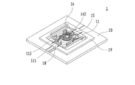
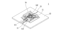
- FIG. 5 is a schematic plan view showing an example of a path of light emitted from a light emitting member in the key switch described in the present application.
- FIG. 5 is a schematic cross-sectional view conceptually showing an example of a path of light emitted from a light emitting member in the key switch described in the present application.
- the key input device described in the present application is used as a keyboard used for inputting data such as various commands in addition to characters, numbers and symbols to an electronic device such as a computer.
- the key input device described in the present application is suitable for applications with high palatability, such as being thin, emitting light, emitting a preferable operation sound, and having an operation feel.
- FIG. 1 is a schematic perspective view showing an example of the appearance of a keyboard KB to which the key input device described in the present application is applied.
- a plurality of key switches 1 such as character keys, numeric keys, and other function keys are arranged side by side on the keyboard KB as a switch device.
- key switches 1 having the same shape are arranged side by side for the purpose of simplifying the structure and easily recognizing the technical contents, but the mounting is limited to such a shape. It's not a thing.
- the key switch 1 having a specific function such as an enter key arranged around the character keys is configured to have a shape different from that of the character keys.
- Etc. it is possible to design as appropriate.
- the keyboard KB placed on the desk by the user in a general posture is used, and the direction of the keyboard KB and the key switch 1 included in the keyboard KB is defined from the user's point of view. .. That is, the front side (lower left side in FIG. 1) is the front side, and the direction in which the key switch 1 is pressed is the lower side.
- the key switch 1 included in the keyboard KB described in the present application can be realized in various forms, and here, as an example thereof, the first embodiment, the second embodiment, and the third embodiment will be illustrated and described. To do.
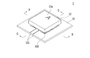
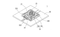
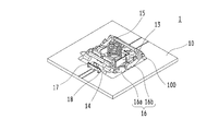
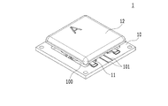
- FIG. 2A and 2B are schematic perspective views showing an example of the appearance of the key switch 1 described in the present application.
- FIG. 2A shows the key switch 1 from an obliquely upper view
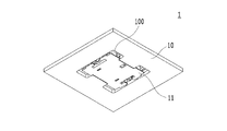
- FIG. 2B shows the key switch 1 from an obliquely lower view.
- the key switch 1 includes a substrate 10 built in the keyboard KB, a fixing member 11 fixed to the substrate 10, and a vertically movable movable member 12 that is pushed downward by a user's pressing operation.
- symbols such as letters, symbols, and numbers (“A” in the example of FIG.
- the code portion 12a corresponding to the code shown on the upper surface of the movable member 12 is made of a translucent resin material so that light can pass through.
- the upper surface of the movable member 12 has a substantially square shape in a plan view.
- the lower surface of the fixing member 11 also has a substantially square shape in a plan view.
- a fitting port 100 is provided in the substrate 10, and the lower portion of the fixing member 11 is fitted in the fitting port 100.
- the fitting opening 100 has a substantially H-shape, the opening corresponding to the H-shaped horizontal bar has a substantially square shape, and the fixing member 11 is fitted into the substantially square-shaped opening.
- a pair of wiring 101 extending forward and rearward from the fitting port 100 is formed on the upper surface of the substrate 10.
- the substrate 10 may be arranged for each key switch 1, and one substrate 10 may be shared by a plurality of key switches 1.
- the keyboard KB As an operation of the keyboard KB, when the user touches the movable member 12 of the key switch 1 and presses the movable member 12, the movable member 12 moves downward by the pressing operation and the pressing operation. When released from the pressing by, the movable member 12 moves upward. When the movable member 12 is moved downward by the operation of pressing the movable member 12, the contact / detachment state of the electric circuit is switched, and the keyboard KB that detects the change of the contact / detachment state is connected to a personal computer or the like. An ON signal for each key switch 1 is output to the electronic device. Further, by releasing the pressing of the movable member 12, the movable member 12 released from the pressing rises and returns to the original position, and the contact / detachment state of the electric circuit also returns to the original position.
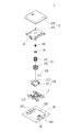
- FIG. 3 is a schematic exploded perspective view showing an example of the key switch 1 described in the present application.
- FIG. 4 is a schematic bottom view showing an example of the key switch 1 described in the present application.
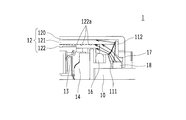
- FIG. 5 is a schematic cross-sectional view showing an example of the internal structure of the key switch 1 described in the present application.
- 6 and 7 are schematic perspective views showing an example of the internal structure of the key switch 1 described in the present application.
- FIG. 8 is a schematic cross-sectional view showing an example of the internal structure of the key switch 1 described in the present application.
- FIG. 5 shows a partially enlarged cross section in the AB direction shown in FIG. 2A
- FIG. 8 shows a cross section in the CD direction shown in FIG. 2A.
- the key switch 1 includes various members such as a contact member 13, a pressing member 14, an elastic member 15, a guide member 16, a translucent member 17, and a light emitting member 18 in addition to the above-mentioned substrate 10, fixing member 11, and movable member 12.
- the movable member 12 includes a key top 120 which is a pressed member for receiving a pressing operation by the user, a light diffusing plate 121, and a light guide plate 122.
- FIG. 6 shows a state in which the movable member 12 is removed from the key switch 1
- FIG. 7 shows the arrangement of other members except the fixed member 11 and the movable member 12 from the key switch 1.
- the fitting port 100 is provided on the substrate 10, and the wiring 101 is formed on the upper surface thereof.
- a light emitting member 18 such as an LED (Light Emitting Diode) that emits light is surface-mounted at the tip of the wiring 101 formed in front of the fitting port 100 (lower left side when facing FIG. 3) on the fitting port 100 side.
- SMT Surface Mount Technology
- the terminal portion 130 of the contact member 13 is surface-mounted at the tip of the wiring 101 formed behind the fitting port 100 (upper right side when facing FIG. 3) on the fitting port 100 side.
- the fixing member 11 is fixed on the substrate 10 in a state where the lower portion is fitted into the fitting port 100 of the substrate 10. As shown in FIGS. 4 and 5, a regulating portion 110 projecting laterally is provided below the fixing member 11 fitted into the fitting opening 100 of the substrate 10. The regulating unit 110 presses the fitting port 100 from the inside and engages with the fitting port 100 to regulate the fitting position of the fixing member 11. That is, the fixing member 11 is fixed in the fitting port 100 of the substrate 10 by the regulating portion 110.
- the fixing member 11 surrounds all or part of the periphery of the light emitting member 18 and secures an optical path region 111 which is an optical path from the light emitting member 18 to the light transmitting member 17.
- the wall 112 of the fixing member 11 forming the optical path region 111 may be in contact with the light emitting member 18 so as to hold the light emitting member 18, or may surround the periphery in a state of being separated so as to embrace the light emitting member 18.
- FIG. 6 shows the optical path region 111 surrounding the light emitting member 18 and the light transmitting member 17 from diagonally above
- FIG. 7 shows the light emitting member 18 and the light transmitting member 18 surrounded by the optical path region 111 by removing the fixing member 11. The arrangement of the members 17 is shown.
- the optical path region 111 illustrated in FIG. 6 is formed as a region inside a rectangular cylinder having a substantially rectangular shape in a plan view, and three of the side surfaces of the square cylinder are surrounded by the wall body 112 and the fitting port 100 side is open. ..
- the wall body 112 forming the optical path region 111 is arranged so as to be in contact with the light emitting member 18 and the light transmitting member 17.
- the key top 120, the light diffusing plate 121, and the light guide plate 122 included in the movable member 12 have a thin plate shape in a square view in a plan view, and the movable member 12 has surfaces of the key top 120, the light diffusing plate 121, and the light guide plate 122. Are assembled so that they overlap.
- the light guide plate 122 receives the incident light emitted from the light emitting member 18 and guides the incident light into a substantially square plate-shaped plane.
- an inclined surface 122a that reflects or refracts incident light spreading in a plane shape upward is formed concentrically, and the light reflected or refracted by the inclined surface 122a is upwardly reflected from the upper surface of the light guide plate 122.
- an inclined surface 122a is formed on the upper surface of the light guide plate 122, and the light guided into the light guide plate 122 is refracted by the inclined surface 122a and heads upward.
- the light diffusing plate 121 receives the incident light emitted from the light emitting member 18 and emitted in a plane shape by the light guide plate 122.
- the light incident on the lower surface of the light diffusing plate 121 from below is diffused in the light diffusing plate 121 and emitted upward from the upper surface.
- the light emitted from the light emitting member 18 and emitted in a planar manner by the light guide plate 122 is diffused in the light diffusing plate 121 to irradiate the key top 120 from below as even planar light.
- the code portion 12a emits light.
- the movable member 12 is provided with an engaging groove 122b in which the pressing member 14 is engaged in a state in which the pressing member 14 can move up and down, and the pressing member 14 engages with the engaging groove 122b of the movable member 12. Guided by the engagement groove 122b, it moves up and down.
- the contact member 13 has a square tubular shape formed by molding and combining two metal plates, and is fitted by press fitting so as to stand upright from the bottom surface of the fixing member 11.
- the terminal portions 130 extend laterally from the two metal plates constituting the contact member 13, and the two terminal portions 130 are soldered onto the wiring 101 formed on the substrate 10.
- the contact member 13 is formed with a contact / detachment portion that opens and closes an electric circuit related to the key switch 1 in response to a pressing action from a pressing member 14 that moves with the movement of the movable member 12.
- the contact / detachment portion of the contact member 13 is configured such that the fixed piece 131 constituting the contact member 13 and the movable piece 132 that bends by pressing are superimposed.
- the movable piece 132 is located outside the fixed piece 131, receives a pressing action from the pressing member 14 accompanying the movement of the movable member 12, and bends inward to come into contact with the fixed piece 131, and the pressing action is released. Then, it returns to the original shape and is separated from the fixed piece 131.
- Contact points are provided on the opposing surfaces of the fixed piece 131 and the movable piece 132, respectively.
- the contact / separation of the fixed piece 131 and the movable piece 132 formed by the two metal plates constituting the contact member 13 is the electricity related to the key switch 1 connected to the two terminal portions 130 of the contact member 13.
- the circuit is opened and closed, and an on signal based on the opening and closing is output from the keyboard KB to the electronic device.
- the pressing member 14 is a member that presses the movable piece 132 of the contact member 13, is attached to the movable member 12 so as to be movable up and down, and moves up and down with the movement of the movable member 12.
- the pressing member 14 includes a pressing portion 140 that presses the contact member 13, and an engaging piece 141 that extends from the pressing portion 140 in a blade shape to the left and right.
- the pressing member 14 is movably engaged with the engaging groove 122b of the movable member 12 by the engaging piece 141, and the engaging groove 122b of the movable member 12 and the engaging piece 141 are engaged with each other. Within the range, it can move up and down relative to the movable member 12. As illustrated in the cross-sectional view of FIG. 8, the pressing portion 140 of the pressing member 14 projects toward the contact member 13.
- the protruding pressing portion 140 is engaged with an engaging protrusion 132a protruding from the movable piece 132 of the contact member 13 toward the pressing member 14.
- FIG. 8 shows a state in which the movable member 12 is not pressed, the pressing portion 140 of the pressing member 14 presses the engaging projection 132a of the movable piece 132 of the contact member 13, and the pressed movable piece 132 is pressed. It is bent. From the state shown in FIG. 8, when the movable member 12 is pressed, the movable member 12 moves downward, but the pressing member 14 does not move from the pressing position due to the engagement with the movable piece 132. , The movable member 12 moves upward relative to the movable member 12.
- the pressing member 14 has a slightly recessed position for pressing the movable piece 132, and is formed so as to engage with the engaging projection 132a of the movable piece 132 so as not to move easily.
- the pressing member 14 reaches the upper limit of movement with respect to the movable member 12, and moves downward together with the movable member 12.
- the pressing member 14 moves further downward from the state in which the movable piece 132 of the contact member 13 is pressed, the movable piece 132 is disengaged from the engaging projection 132a and the pressing is released.
- the movable piece 132 moves like a leaf spring, returns from the bending position, and switches between the contact and detachment states.
- the electric circuit related to the key switch 1 opens / closes, and an on signal based on the opening / closing is output from the keyboard KB to the electronic device.
- the movable piece 132 is disengaged, the pressing member 14 moves downward relative to the movable member 12 due to gravity.
- the load for pressing the movable member 12 changes, and the movable piece 132 of the contact member 13 returns from the flexed position so that the leaf spring can be popped. Because it does, a sound is generated.
- the user recognizes the change in load as a click feeling, and recognizes the generated sound as a click sound.
- the elastic member 15 is a member having elasticity such as a compression coil spring, the lower end side is fixed to the fixing member 11, and the upper end side presses the lower surface of the movable member 12. Therefore, when the movable member 12 is pushed and moves downward, the elastic member 15 is compressed, and when the movable member 12 is released from the push, the elastic member 15 pushes the movable member 12 upward.
- the guide member 16 is formed by combining the first link member 16a and the second link member 16b.
- the first link member 16a is substantially U in which two arm portions 161 having a swing shaft 160 on the first end side are connected by a connecting portion 162 formed on the second end side opposite to the first end side. It has a character shape.
- the second link member 16b also has substantially the same shape as the first link member 16a.
- the guide member 16 is a member formed by combining the swing shaft 160 of the first link member 16a and the swing shaft 160 of the second link member 16b to form a substantially V-shape in a side view, and the first link member 16a and the second link member 16 The link member 16b is combined so that the V-shape opens and closes with the swing shaft 160 as the swing center.
- the swing shaft 160 of the guide member 16 is fixed to the fixing member 11, and the connecting portion 162 of the first link member 16a and the second link member 16b forming the guide member 16 moves to the bottom surface side of the movable member 12.
- the guide member 16 has a function of guiding the movable member 12 so that the upper surface of the movable member 12 does not tilt when the movable member 12 moves up and down. That is, when the movable member 12 moves downward, the connecting portion 162 of the guide member 16 moves so as to be separated from each other on the bottom surface side of the movable member 12, so that the V-shape of the guide member 16 maintains a substantially plane-symmetrical state. Since it opens while opening, the movable member 12 moves downward without tilting. The same applies when the movable member 12 moves upward, and the movable member 12 is guided by the guide member 16 and moves upward without tilting.
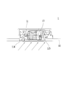
- FIG. 9 is a schematic cross-sectional view conceptually showing an example of the path of light emitted from the light emitting member 18 in the key switch 1 described in the present application.
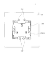
- FIG. 10 is a schematic plan view showing an example of the path of light emitted from the light emitting member 18 in the key switch 1 described in the present application.
- the arrows conceptually indicate the path of light.
- the light emitting member 18 of the key switch 1 is arranged on the substrate 10 by surface mounting, and the light transmitting member 17 is arranged at a position near the fitting port 100 above the light emitting member 18.
- the light emitting member 18 arranged on the substrate 10 emits light upward.
- upward means to a position above the light emitting member 18, and includes not only directly above but also diagonally above.
- the light emitted upward from the light emitting member 18 travels directly above or diagonally upward through the optical path region 111 formed by the wall body 112 of the fixing member 11, and is incident on the light transmitting member 17 from the lower surface side. To do.
- the translucent member 17 has a substantially square columnar shape, and the upper surface is inclined toward the inside (fitting port 100 side). The light incident from the lower surface side of the translucent member 17 passes through the translucent member 17 and is emitted from the upper surface. Since the upper surface of the translucent member 17 is inclined inward, the light emitted through the translucent member 17 is refracted inward on the upper surface, and the light guide plate attached to the lower surface side of the movable member 12. It is incident on 122.
- FIG. 9 illustrates a form in which light is emitted obliquely upward from the translucent member 17, but if the light is incident on the light guide plate 122 attached to the lower surface of the movable member 12, the translucent member 17 is used.
- the light may be emitted directly upward. That is, light is emitted from the light transmitting member 17 toward the upper side, which is directly above or diagonally above, and is incident on the light guide plate 122.
- the light emitted from the light transmitting member 17 is emitted toward one side of the light guide plate 122 having a rectangular shape in a plan view.
- the light guide plate 122 is concentrically formed with inclined surfaces 122a, and the light emitted from the light transmitting member 17 is directed to the center of the concentric circles formed on the light guide plate 122 as inclined surfaces 122a. It is irradiated toward.
- the light incident on the light guide plate 122 is guided in the light guide plate 122 as shown by an arrow in FIG. 10, and spreads concentrically in the light guide plate 122 while repeating reflection on the upper surface and the lower surface of the light guide plate 122.
- the light traveling in the light guide plate 122 hits the inclined surface 122a, it changes its course upward by reflection or refraction.
- the light is emitted from the upper surface of the light guide plate 122 and incident on the light diffusing plate 121 from the lower surface.
- the light incident on the light guide plate 122 spreads concentrically in the light guide plate 122 and is emitted from the upper surface, so that the light is uniformly emitted from the entire upper surface.
- the light emitted from the entire upper surface of the light guide plate 122 is incident on the lower surface of the light diffusing plate 121.
- the light incident on the light diffusing plate 121 from the lower surface diffuses in the light diffusing plate 121 and is emitted from the upper surface as planar light, and irradiates the key top 120 located at the upper part of the movable member 12 from below. Since the light emitted from the light guide plate 122 is diffused to some extent in the light diffusing plate 121 and then irradiated upward, the key top 120 is further irradiated from below as uniform light with no unevenness in a plan view. When the key top 120 is irradiated from below, the code portion 12a formed of the translucent resin material emits light.
- FIG. 11 is a schematic cross-sectional view conceptually showing an example of the path of light emitted from the light emitting member 18 in the key switch 1 described in the present application.
- the key switch 1 shows a state in which the key top 120 is pressed and the movable member 12 is lowered.
- the arrows conceptually indicate the path of light.
- the distance between the translucent member 17 and the light guide plate 122 changes, so that the optical path changes.
- the light emitted from the light transmitting member 17 and incident on the light guide plate 122 is incident on the light diffuser plate 121 from below as planar light in the light guide plate 122, diffused by the light diffuser plate 121, and is a key top. Since the 120 is irradiated, the influence of the code portion 12a of the key top 120 on the light emission is suppressed. Since the movable member 12 is in the state where the user places his / her finger on the key top 120, the optical design of the members such as the translucent member 17 and the light diffusing plate 121 is The design will be based on the position where the movable member 12 is at the top.
- the key switch 1 provides a highly palatable keyboard KB because the key top 120 is illuminated by the light emitted from the light emitting member 18 surface-mounted on the substrate 10. Is possible. Moreover, since the lower portion of the fixing member 11 is fitted into the fitting opening 100 provided in the substrate 10, the height as a whole can be lowered and a thin keyboard KB can be provided. Although it is possible to arrange the light emitting member 18 directly below the central portion of the key top 120 in order to make the key top 120 shine, in that case, the height as a whole may increase. In the key switch 1 described in the present application, the light emitting member 18 can be surface-mounted on the substrate 10 on the side of the fixing member 11 to realize a thinning.
- the key top 120 is irradiated not from the center but by the light emitting member 18 arranged on the side, but the key switch 1 described in the present application suppresses light emission unevenness by the light guide plate 122 and the light diffusing plate 121. It is possible to do.
- the key switch 1 described in the present application according to the second embodiment has a form in which some members such as a fixing member 11, a pressing member 14, and a guide member 16 are changed and a new member is added in the first embodiment. is there.
- some members such as a fixing member 11, a pressing member 14, and a guide member 16 are changed and a new member is added in the first embodiment. is there.
- the same configurations as those of the first embodiment are designated by the same reference numerals as those of the first embodiment, and the first embodiment will be referred to, and detailed description thereof will be omitted.
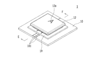
- FIG. 12 is a schematic perspective view showing an example of the appearance of the key switch 1 described in the present application.
- FIG. 12 shows the key switch 1 from an obliquely upward viewpoint.
- the key switch 1 includes members such as a substrate 10, a fixing member 11, and a movable member 12, and a light-shielding plate 19 is further arranged on the substrate 10.
- the light-shielding plate 19 has a substantially square shape in a plan view, and has a substantially square shape in a plan view formed inside, and has a frame shape as a whole.
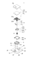
- FIG. 13 is a schematic exploded perspective view showing an example of the key switch 1 described in the present application.
- FIG. 14 is a schematic cross-sectional view showing an example of the internal structure of the key switch 1 described in the present application.
- 15 and 16 are schematic perspective views showing an example of the internal structure of the key switch 1 described in the present application.
- FIG. 14 shows a cross section in the EF direction shown in FIG.
- the key switch 1 includes the above-mentioned substrate 10, fixing member 11, movable member 12, light-shielding plate 19, contact member 13, pressing member 14, elastic member 15, guide member 16, light-transmitting member 17, light-emitting member 18, and the like. It is equipped with various members.
- the light diffusing plate 121 is integrated with the key top 120.
- the pressing member 14 includes an urging member 142 such as a compression coil spring.
- FIG. 15 shows a state in which the movable member 12 and the light-shielding plate 19 are removed from the key switch 1
- FIG. 16 shows a state in which the fixed member 11, the movable member 12, and the light-shielding plate 19 are removed from the key switch 1 and other members. Shows the placement.
- a fitting port 100 is provided on the substrate 10, and a terminal portion 130 of the light emitting member 18 and the contact member 13 is surface-mounted on the wiring 101 formed on the upper surface.
- the lower portion of the fixing member 11 is fitted into the fitting port 100 of the substrate 10.
- the fixing member 11 is formed with an optical path region 111 that surrounds all or part of the periphery of the light emitting member 18 and serves as an optical path from the light emitting member 18 to the light transmitting member 17.
- the optical path region 111 illustrated in FIGS. 15 and 16 is formed as a region inside a rectangular cylinder having a substantially rectangular shape in a plan view, and three of the side surfaces of the square cylinder are surrounded by the wall body 112, which is opposite to the fitting opening 100. The outside on the side is open.
- the wall body 112 forming the optical path region 111 surrounds the light emitting member 18 and the light transmitting member 17 in a state of being separated so as to embrace them.
- the opening of the light-shielding plate 19 arranged on the upper surface of the substrate 10 is formed so as to be slightly smaller than the fitting port 100 provided in the substrate 10, and the light-shielding plate 19 is formed so as to be slightly smaller than the fitting port 100 of the substrate 10. It is arranged so as to cover the edge of the.
- the light-shielding plate 19 that covers the edge of the fitting port 100 of the substrate 10 covers the outer surface of the optical path region 111 formed in the fixing member 11 that is not surrounded by the wall body 112.
- the light-shielding plate 19 prevents the light emitted from the light-emitting member 18 from leaking from a portion other than the key top 120.
- the movable member 12 includes a key top 120 and a light guide plate 122, and a columnar guide pillar 123 extending downward is provided so as to project near the center of the lower surface.
- the pressing member 14 included in the key switch 1 according to the second embodiment has a substantially cylindrical shape, and a guide pillar 123 projecting from the lower surface of the pressing member 14 is inserted into the central opening. The pressing member 14 is guided by the inserted guide pillar 123 and is held so as to be movable in the vertical direction with respect to the movable member 12.
- a mounting groove 143 in the circumferential direction surrounding the opening is engraved from the upper surface side on the side wall forming the cylinder of the pressing member 14, and the lower end of the urging member 142 such as a compression coil spring is fitted in the mounting groove 143. It is installed in a closed state.
- a pressing portion 140 that presses the contact member 13 projects from the outer surface of the pressing member 14.
- FIG. 14 shows a state in which the movable member 12 is not pressed, and the pressing portion 140 protruding from the pressing member 14 is in contact with the upper side of the engaging portion 113 erected on the bottom surface of the fixing member 11. ..
- the movable member 12 moves downward, but the pressing member 14 is in a state of being supported from below by the engaging portion 113 and is pressed from the pressing position. Since it does not move, it moves relatively upward with respect to the movable member 12. Further, when the movable member 12 moves downward, the upper portion of the urging member 142 is pressed against the lower surface of the movable member 12 to compress it, and the pressing member 14 is urged downward.
- the guide member 16 is formed by combining the first link member 16a and the second link member 16b.
- the first link member 16a and the second link member 16b according to the second embodiment are arranged apart from each other.
- the mechanism in which the light emitted from the light emitting member 18 irradiates the key top 120 from the lower surface side and illuminates the key top 120 is substantially the same as that of the first embodiment.
- the embodiment shall be referred to.
- the key switch 1 according to the second embodiment can provide a highly palatable keyboard KB in which the key top 120 shines, and provides a thin keyboard KB, as in the first embodiment. It is possible.
- the key switch 1 described in the present application according to the third embodiment does not mount the terminal portion 130 of an electronic member such as a contact member 13 on the substrate 10 as a surface mount component in the first embodiment, but penetrates the substrate 10. It is a form of mounting as a DIP component.
- the same configurations as those of the first embodiment are designated by the same reference numerals as those of the first embodiment, and the first embodiment will be referred to, and detailed description thereof will be omitted.
- FIG. 17A and 17B are schematic perspective views showing an example of the appearance of the key switch 1 described in the present application.
- FIG. 17A shows the key switch 1 from an obliquely upper view
- FIG. 17B shows the key switch 1 from an obliquely lower view.
- Four insertion ports 102 for fixing the fixing member 11 on the substrate 10 are provided on the lower surface of the substrate 10, and the anchor portion 114 included in the fixing member 11 is inserted into the insertion port 102.
- the terminal portion 130 made of the conductive metal of the contact member 13 is exposed from the lower surface of the fixing member 11 exposed from the fitting port 100 provided on the substrate 10.
- FIG. 18 is a schematic exploded perspective view showing an example of the key switch 1 described in the present application.
- FIG. 19 is a schematic cross-sectional view showing an example of the key switch 1 described in the present application.
- FIG. 19 shows a cross section in the GH direction shown in FIG. 17A.
- the key switch 1 includes various members such as a contact member 13, a pressing member 14, an elastic member 15, a guide member 16, a translucent member 17, and a light emitting member 18 in addition to the above-mentioned substrate 10, fixing member 11, and movable member 12. ing.
- a fitting port 100 is provided on the substrate 10, and the lower portion of the fixing member 11 is fitted into the fitting port 100 of the substrate 10.
- a wiring 101 is formed on the upper surface of the substrate 10, and a light emitting member 18 is mounted as a surface mount component on the wiring 101 of the substrate 10.
- the terminal portion 130 of the contact member 13 penetrates the fixing member 11 and is exposed from the lower surface of the fixing member 11.
- the fixing member 11 is formed with an anchor portion 114 extending from the side portion onto the substrate 10 and having a tip bent downward, and the anchor portion 114 is a difference provided in the substrate 10. It is inserted into the inlet 102.
- the tip of the anchor portion 114 inserted into the insertion port 102 is bifurcated, and by pressing the inner wall surface inside the insertion port 102 from the inside, it becomes difficult to pull out from the insertion port 102.
- the fixing member 11 is fixed on the substrate 10 by inserting the anchor portion 114 of the fixing member 11 into the insertion port 102 provided in the substrate 10. Further, by inserting the anchor portion 114 into the insertion port 102, the key switch 1 itself is also fixed to the substrate 10.
- the mechanism in which the light emitted from the light emitting member 18 irradiates the key top 120 from the lower surface side and illuminates the key top 120 is substantially the same as that of the first embodiment.
- the embodiment shall be referred to.
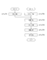
- FIG. 20 is a flowchart showing an example of a method for manufacturing the key switch 1 described in the present application.
- a manufacturing method of the key switch 1 first, an assembly step of attaching various members such as a movable member 12, a contact member 13, a pressing member 14, an elastic member 15, a guide member 16, and a translucent member 17 to a fixing member 11 and assembling the key switch 1. Is carried out (step S1).
- the wiring 101 is formed on the substrate 10.
- Cream solder is applied onto the wiring 101 of the formed substrate 10, and a reflow step of soldering the light emitting member 18 is carried out (step S2).
- a fitting step of fitting the lower part of the fixing member 11 which is a part of the key switch 1 assembled in step S1 into the fitting opening 100 opened in the substrate 10 is performed (step S3).
- the light emitting member 18 may be accommodated in the fixing member 11 after the light emitting member 18 is soldered onto the substrate 10, and the light emitting member may be housed in the fixing member 11 in the assembly step.
- the light emitting member 18 in a state in which the 18 is housed and housed in the fixing member 11 may be soldered onto the substrate 10. That is, the steps of steps S1 to S3 can be appropriately changed, and as a result, the light emitting member 18 is surface-mounted on the substrate 10, and a part or all of the periphery of the surface-mounted light emitting member 18 is fixed. It may be accommodated so as to be surrounded by 11, and the lower portion of the fixing member 11 may be fitted into the fitting opening 100 provided in the substrate 10.
- These processes can be changed as appropriate, and it is also possible to appropriately design the processes including the distribution form, such as carrying out these processes in different business entities.
- FIG. 21 is a schematic bottom view showing an example of the appearance of the key switch 1 described in the present application.
- FIG. 21 shows the key switch 1 after the fitting step is carried out in step S3 from the viewpoint from below.
- a heat-resistant sheet 115 made of a resin film is detachably attached to the lower surface of the fixing member 11.
- the heat-resistant sheet 115 is cut according to the shape of the fitting port 100, and covers the exposed portion of the lower surface of the fixing member 11.
- the periphery of the terminal portion 130 of the electronic member such as the contact member 13 exposed from the lower surface of the fixing member 11 is hollowed out, and the terminal portion 130 is exposed from the heat-resistant sheet 115.
- the heat-resistant sheet 115 may be attached before or after the fixing member 11 is fitted into the fitting opening 100.
- solder is applied to the terminal portion 130 of the electronic member such as the contact member 13 exposed from the fixing member 11 fitted in the fitting port 100 from the lower surface side of the substrate 10.
- the flow process is carried out (step S4).
- FIG. 22 is a schematic cross-sectional view conceptually showing an example of a flow process for the key switch 1 described in the present application.
- the arrow in FIG. 22 indicates the molten solder applied in the flow process.
- solder is applied to the terminal part 130 of the electronic member such as the contact member 13, but since the parts other than the terminal part 130 are protected by the heat-resistant sheet 115, the heat inside the flow process causes the inside. Prevents adverse effects on the members.
- the anchor portion 114 prevents the members such as the fixing member 11 from being lifted from the substrate 10 and the key.
- the switch 1 is fixed to the substrate 10.
- a peeling step of peeling the heat-resistant sheet 115 attached to the lower surface of the fixing member 11 is performed (step S5), and the soldered terminal portion 130 is soldered.
- the process is carried out (step S6).
- the peeling step shown in step S5 is not always necessary, and the soldering step may be carried out with the heat-resistant sheet 115 attached.
- a key top 120 is attached to each attached key switch 1, and the key switch 1 to which the key top 120 is attached is attached to a key input device such as a keyboard KB or a notebook PC.
- the key switch 1 according to the third embodiment can provide a highly palatable keyboard KB in which the key top 120 shines, and provides a thin keyboard KB, as in the first embodiment. It is possible. Further, in the key switch 1 according to the third embodiment, the fixing member 11 is firmly fixed by inserting the anchor portion 114 provided in the fixing member 11 into the insertion port 102 of the substrate 10, and the fixing member 11 and the like are firmly fixed. It is possible to prevent the member of the above from rising. Further, by using the heat-resistant sheet 115 in the production of the key switch 1 according to the third embodiment, it is possible to prevent the internal members from being adversely affected by the heat during the flow process.
- the key switch 1 described in the present application according to the fourth embodiment is a form in which the contact member 13 is integrally molded with the resin by an insert mold in the above-described embodiment.
- the same configurations as those in the above-described embodiment will be designated by the same reference numerals as those in the above-described embodiment, and the above-described embodiments will be referred to, and detailed description thereof will be omitted.
- FIG. 23A and 23B are schematic perspective views showing an example of the appearance of the key switch 1 described in the present application.
- FIG. 23A shows the key switch 1 from an obliquely upper view
- FIG. 23B shows the key switch 1 from an obliquely lower view.
- FIG. 24 is a schematic exploded perspective view showing an example of the key switch 1 described in the present application.
- the key switch 1 includes various members such as a substrate 10, a fixing member 11, a movable member 12, a contact member 13, a pressing member 14, an elastic member 15, a guide member 16, and a light emitting member 18.
- a fitting port 100 is provided on the substrate 10, and a light emitting member 18 is surface-mounted on the wiring 101 formed on the upper surface.
- the lower part of the fixing member 11 is fitted into the fitting port 100 of the substrate 10.
- the contact member 13 is fitted and fixed to the fixing member 11 as a molding contact 134 integrally molded with the mold resin 133 by an insert mold.
- the molded contact 134 fitted in the fixing member 11 is fixed from above by the dust cover 135 formed by molding a metal plate, and the dust cover 135 dusts the contact / detachment portion of the contact member 13 molded in the molded contact 134. Protects from.
- the elastic member 15 two elastic members 150 having a large radius and a second elastic member 151 having a small radius are used in combination so that their central axes coincide with each other.
- a resin-made lower plate 124 having a substantially rectangular shape is fitted on the lower surface of the movable member 12.
- a part of the long side of the lower plate 124 is open so as not to block the light emitted upward from the light emitting member 18.
- the schematic exploded perspective view of FIG. 24 shows a state in which the light diffusing plate 121 and the light guide plate 122 are fitted inside the key top 120, so that the light diffusing plate 121 and the light guide plate 122 are not shown.
- the lower plate 124 of the movable member 12 holds the pressing member 14 in a state where it can move up and down, and the pressing member 14 is urged downward by the urging member 142.
- the pressing member 14 is in contact with the upper side of the engaging portion 113 erected on the bottom surface of the fixing member 11.
- the movable member 12 is pressed against the pressing member 14 held in a state of being movable up and down, the urging member 142 that urges the pressing member 14, and the engaging portion 113 that abuts on the pressing member 14 from below. By doing so, they cooperate to open and close the contact / detachment portion of the contact member 13 to generate a sound.
- the opening / closing of the contact member 13 and the generation of the click feeling and the click sound based on the pressing of the movable member 12 are substantially the same as those in the second embodiment.
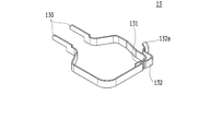
- FIG. 25 is a schematic perspective view showing an example of the contact member 13 included in the key switch 1 described in the present application.
- the contact member 13 is formed by molding and combining two metal plates.
- the terminal portion 130 extends from each of the two metal plates constituting the contact member 13.
- the contact member 13 is formed with a contact / detachment portion that opens and closes an electric circuit related to the key switch 1 in response to a pressing action from a pressing member 14 that moves with the movement of the movable member 12.
- the contact / detachment portion of the contact member 13 is configured such that the fixed piece 131 constituting the contact member 13 and the movable piece 132 that bends by pressing overlap with each other.
- the movable piece 132 is located outside the fixed piece 131, and receives a pressing action from the pressing member 14 accompanying the movement of the movable member 12 by the engaging projection 132a and bends inward to form the fixed piece 131.
- the pressing action is released, the original shape is restored and the fixed piece 131 is separated from the fixed piece 131.
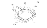
- FIG. 26 is a schematic perspective view showing an example of the molded contact 134 included in the key switch 1 described in the present application.
- the molded contact 134 is formed by integrally molding a contact member 13 obtained by molding and combining two metal plates that open and close a circuit by contact / separation with a mold resin 133 by insert molding.
- the mold resin 133 used for the insert mold to form the molding contact 134 is, for example, an insulating thermoplastic resin, and is molded so as to substantially completely seal the resin along the shape of the contact member 13. However, the terminal portion 130 and the contact / detachment portion of the contact member 13 are exposed from the mold resin 133.
- the mold resin 133 of the molding contact 134 has a substantially annular shape with an open central portion. Further, in the mold resin 133 of the molding contact 134, three positioning grooves 133a used for positioning when fitting into the fixing member 11 are formed as notches on the side portions.
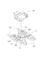
- FIG. 27 is a schematic perspective view showing an example of an assembly process of the fixing member 11 and the molding contact 134 included in the key switch 1 described in the present application.
- FIG. 27 conceptually shows a step of fitting the molded contact 134 in which the contact member 13 is molded by the insert mold into the fixing member 11.
- the fixing member 11 is formed with a fitting recess 116 having a substantially rectangular shape in a plan view into which the molding contact 134 is fitted, and three positioning protrusions 116a are erected along the wall surface forming the fitting recess 116. Has been done.
- an interference prevention wall 116b forming a double concentric circle in a plan view is erected from the bottom surface.
- the outer shape and dimensions of the molded contact 134 are designed based on the outer shape and dimensions of the fitting recess 116, and the opening in the central portion of the molded contact 134 is the outer shape and outer shape of the outer interference prevention wall 116b. Designed based on dimensions.
- the fitting recess 116 is formed with irregularities not only in the above-mentioned shape but also in other portions such as substantially rectangular corners, and the outer diameter of the molded contact 134 is determined based on the formed irregularities.
- the shape is designed.
- a pair of link holes 117 for swingably attaching the first link member 16a and the second link member 16b of the guide member 16 are formed on the side surface of the fixing member 11. Further, on the side surface of the fixing member 11, four fixing metal fittings (holddowns) 118 for fixing in the fitting opening 100 of the substrate 10 are fitted.
- FIG. 28 is a schematic perspective view showing an example of an assembly process of the fixing member 11, the molded contact 134, and other members included in the key switch 1 described in the present application.
- FIG. 28 shows a state in which another member is attached to the fixing member 11 into which the molding contact 134 is fitted.
- the molding contact 134 is fitted into the fixing member 11, and the positioning groove 133a of the molding contact 134, the opening of the central portion, and the like are fitted with the corresponding portions such as the positioning protrusion 116a and the interference prevention wall 116b, respectively. ing.
- the molding contact 134 is fixed in the fixing member 11 by crimping the upper end portion of the positioning protrusion 116a. Further, the dust cover 135 is fixed in a crimped state on the upper side of the molded contact 134 fitted in the fixing member 11.
- a first elastic member 150 is attached between the outer wall and the inner wall of the interference prevention wall 116b erected in a double concentric circle, and the second elastic member 151 is placed inside the inner wall. It is attached.
- the operation of the movable member 12 can be stabilized.
- the double interference prevention wall 116b interference between the first elastic member 150 and the second elastic member 151 can be prevented and the operation can be stabilized.
- a pressing member 14 and an urging member 142 are arranged inside the second elastic member 151. The pressing member 14 and the urging member 142 may be attached to the fixing member 11 side after being attached to the movable member 12.
- the swing shaft 160 of the first link member 16a and the second link member 16b of the guide member 16 is swingably attached to the link hole 117 formed on the side surface of the fixing member 11.
- the key switch 1 is manufactured by a series of assembly steps of attaching other members such as the movable member 12 and further fitting them into the substrate 10.
- the contact member 13 obtained by molding and combining two metal plates that open and close the circuit by contact / separation is integrally molded with the resin by insert molding.
- a molding contact 134 is formed, and the formed molding contact 134 is fixed by fitting it into the fixing member 11.
- the contact member 13 can be stably fixed in the fixing member 11, and other excellent effects can be obtained.
- the height of the key switch 1 itself is also required to be low.
- the method of fixing the molded contact 134 formed by the insert mold to the fixing member 11 fixes the contact member 13 to the fixing member 11 even when the height of the fixing member 11 is lowered as compared with other fixing methods such as press fitting. It is possible to improve the performance such as stability and durability when the product is used. Specifically, it is possible to suppress the wobbling of the contact member 13 and increase the durability against various pressings such as repeated pressing, strong pressing, and fast pressing by the pressing member 14. Such an improvement in performance becomes more remarkable as the height of the fixing member 11 is lowered, and it is possible to meet the demand for a thinner keyboard KB.
- the key switch 1 described in the present application is highly palatable and can provide a thin keyboard KB.
- the first to fourth embodiments can be combined as appropriate, rather than being different forms.
- the pressing member 14 according to the second embodiment can be appropriately designed by applying it to the third embodiment.
- one key switch 1 includes one light emitting member 18, but the present invention is not limited to this, and one key switch 1 has a plurality of light emitting members 18. It is possible to design as appropriate, such as providing. Specifically, the light emitting members 18 are arranged at opposite positions on the substrate 10, for example, near the two opposite sides of the substantially square fitting port 100, and the key tops 120 included in the movable member 12 are respectively arranged. It is possible to design as appropriate, such as irradiating from the opposite direction. By arranging a plurality of light emitting members 18, the light of the key top 120 becomes stronger, and the uniformity of the light can be improved.
- the embodiment applied to a key input device such as a keyboard KB that mainly inputs characters has been shown, but the present invention is not limited to this.
- the key input device KB it is possible to realize the key input device KB as a notebook PC equipped with the key switch 1 described in the present application.
- it can be applied to a key input device KB dedicated to number keys such as a numeric keypad, and various other key input devices KB such as various switches used for electronic devices other than computers, for example, game machines. is there.
- the key switch 1 for fixing the contact member 13 by the insert mold exemplified as the fourth embodiment can be applied to various key switches 1 such as a form in which the light emitting member 18 is not provided and a form in which the light emitting member 18 is attached by a different method. It is possible to apply.
- KB keyboard (key input device) 1 key switch (switch device) 10 Board 100 Fitting port 102 Insertion port 11 Fixing member 110 Restricting part 111 Optical path area 112 Wall body 113 Engaging part 114 Anchor part 115 Heat-resistant sheet 116 Fitting recess 12 Movable member 120 Key top (pressed member) 121 Light diffusion plate 122 Light guide plate 122a Inclined surface 13 Contact member 130 Terminal part 133 Molded resin 134 Molded contact 17 Light transmitting member 18 Light emitting member 19 Light shielding plate
Landscapes
- Engineering & Computer Science (AREA)
- General Engineering & Computer Science (AREA)
- Theoretical Computer Science (AREA)
- Human Computer Interaction (AREA)
- Physics & Mathematics (AREA)
- General Physics & Mathematics (AREA)
- Manufacturing & Machinery (AREA)
- Push-Button Switches (AREA)
Abstract
嗜好性が高く、薄型化が可能なスイッチ装置、キー入力装置及びスイッチ装置を提供する。 キー入力装置に使用可能なスイッチ装置1は、基板10に固定される固定部材11と、固定部材11に移動可能に支持され、押下操作により押下方向へ移動する可動部材12とを備えている。可動部材12の上部には、押下操作を受け付ける被押下部材120(キートップ)が取り付けられており、可動部材12が押下方向へ移動する過程で電気的な接離状態が切り替わる。基板10上には、発光部材18が配設されており、発光部材18から発せられた光は、被押下部材120を下側から照射する。また、固定部材11の下部は、基板10に開設された嵌着口100に嵌め込まれている。
Description
本発明は、可動部材を押下することにより電気的な接離状態を切り替えるスイッチ装置、そのようなスイッチ装置を備えるキー入力装置、及びそのようなスイッチ装置を製造するスイッチ装置の製造方法に関する。
コンピュータ等の電子機器への入力装置として、複数のキースイッチが並べて配設されたキーボード、更には、入力装置を備える電子機器本体となるノート型パーソナルコンピュータ(以下、ノートPCという)が普及している。例えば、特許文献1には、プリント基板にスイッチ実装用穴を設けスイッチ本体の一部を該穴に落とし込む基板実装用小型押ボタンスイッチが開示されている。また、昨今では、例えば、eスポーツと呼ばれるコンピュータゲーム等の嗜好性の高い分野に用いられるキーボード及びノートPCの仕様に対して、様々な要求がある。キーボードへの要求としては、薄型化等の形状面での要求、キートップの上面の発光等の機能面での要求等の要求を例示することができる。
しかしながら、特許文献1に記載されたスイッチは、プリント基板のスイッチ実装用穴にスイッチ本体の一部を落とし込むことで薄型化に繋げることはできても、スイッチ本体内に発光用の部材を配設すると厚みが増す可能性がある。
本発明は斯かる事情に鑑みてなされたものであり、薄型化、発光等の様々な要求を満たすことが可能なスイッチ装置の提供を主たる目的とする。
また、本発明は、そのようなスイッチ装置を用いたキーボード等のキー入力装置の提供を他の目的とする。
また、本発明は、そのようなスイッチ装置を製造するスイッチ装置の製造方法の提供を更に他の目的とする。
上記課題を解決するため、本願記載のスイッチ装置(キースイッチ)は、基板に固定可能な固定部材と、前記固定部材に移動可能に支持され、押下操作により押下方向へ移動する可動部材とを備え、前記可動部材の上部には、押下操作を受け付ける被押下部材が取付可能であり、前記可動部材が押下方向へ移動する過程で電気的な接離状態が切り替わるスイッチ装置であって、前記固定部材は、上面に発光部材が配設された前記基板に開設されている嵌着口に、下部が嵌め込み可能に形成されており、前記発光部材が配設された前記基板の嵌着口に、下部が嵌め込まれた場合に、前記発光部材から発せられた光が、前記可動部材の上部に取り付けられる前記被押下部材を照射可能に形成されていることを特徴とする。
更に、本願記載のスイッチ装置は、基板に固定可能な固定部材と、前記固定部材に移動可能に支持され、押下操作により押下方向へ移動する可動部材とを備え、前記可動部材の上部には、押下操作を受け付ける被押下部材が取り付け可能であり、前記可動部材が押下方向へ移動する過程で電気的な接離状態が切り替わるスイッチ装置であって、前記基板上に配設される発光部材を備え、前記固定部材の下部は、前記基板に開設された嵌着口に嵌め込まれており、前記発光部材から発せられた光は、前記可動部材の上部に取り付けられる前記被押下部材を照射することを特徴とする。
また、本願記載のスイッチ装置において、前記発光部材から発せられた光を、前記被押下部材の下方から照射するように通す透光部材を備えることを特徴とする。
また、本願記載のスイッチ装置において、前記固定部材は、前記発光部材を囲い、前記発光部材から前記透光部材までの光路となる光路領域が確保されていることを特徴とする。
また、本願記載のスイッチ装置において、前記被押下部材の下面側に取り付けられ、入射光を内部で拡散する光拡散板を備え、前記発光部材から発せられた光は、前記光拡散板に入射し、前記光拡散板内で拡散して、前記被押下部材を下方から照射することを特徴とする。
また、本願記載のスイッチ装置において、前記被押下部材の下面側に取り付けられ、入射光を導く導光板を備え、前記導光板は、入射した光を反射又は屈折させて上方へ出射させる傾斜面を有することを特徴とする。
また、本願記載のスイッチ装置において、前記固定部材は、前記嵌着口と係合して嵌着位置を規制する規制部を備えることを特徴とする。
また、本願記載のスイッチ装置において、前記固定部材は、前記嵌着口とは別に前記基板に開設された差込口に差し込むアンカー部を備えることを特徴とする。
また、本願記載のスイッチ装置において、前記固定部材の下面に剥離可能に貼付された耐熱シートを備えることを特徴とする。
また、本願記載のスイッチ装置において前記固定部材に対して、前記可動部材を傾くことなく移動可能に案内する案内部材を備えることを特徴とする。
また、本願記載のスイッチ装置において、前記固定部材の下部を嵌め込む嵌着口が開設された基板を備えることを特徴とする。
また、本願記載のスイッチ装置において、接触/離隔により回路を開閉する複数の金属を成型して組み合わせた接点部材を、インサートモールドにて樹脂と一体成型してなる成型接点を備え、前記成型接点は、前記固定部材に固定されていることを特徴とする。
更に、本願記載のスイッチ装置は、基板に固定可能な固定部材と、前記固定部材に移動可能に支持され、押下操作により押下方向へ移動する可動部材とを備え、前記可動部材の上部には、押下操作を受け付ける被押下部材が取付可能であり、前記可動部材が押下方向へ移動する過程で電気的な接離状態が切り替わるスイッチ装置であって、接触/離隔により回路を開閉する複数の金属を成型して組み合わせた接点部材を、インサートモールドにて樹脂と一体成型してなる成型接点を備え、前記成型接点は、前記固定部材に固定されていることを特徴とする。
更に、本願記載のキー入力装置(キーボード、ノートPC)は、複数のキースイッチが配設されたキー入力装置であって、配設されたキースイッチとして、前記スイッチ装置を備えることを特徴とする。
更に、本願記載のスイッチ装置の製造方法は、基板と、前記基板に固定された固定部材と、前記固定部材に移動可能に支持され、押下操作により押下方向へ移動する可動部材と、前記可動部材の上部に取り付けられ、押下操作を受け付ける被押下部材とを備え、前記可動部材が押下方向へ移動する過程で電気的な接離状態が切り替わるスイッチ装置の製造方法であって、基板上に発光部材を半田にて表面実装するリフロー工程と、前記基板に開設された嵌着口に、前記固定部材の下部を嵌め込む嵌着工程と、前記嵌着口に嵌め込まれた前記固定部材から露出する端子部を、前記基板の下面側から半田を塗布するフロー工程とを実行することを特徴とする。
また、本願記載のスイッチ装置の製造方法において、前記固定部材の底面には、耐熱シートが貼付されており、前記フロー工程にて、半田を塗布した後、前記耐熱シートを剥離する剥離工程を実行することを特徴とする。
本願記載のスイッチ装置及びキー入力装置、並びにスイッチ装置の製造方法で製造されるスイッチ装置は、基板上に発光部材が配設され、固定部材の下部が基板に開設された嵌着口に嵌め込まれている。
本発明では、基板上に発光部材を配設し、基板に開設された嵌着口に固定部を嵌め込み、発光部材から発せられる光により、押下部材を照光可能とする。これにより、薄型化、嗜好性の向上等の様々な効果を奏する。
<適用例>
以下、本発明の実施形態について図面を参照しながら説明する。本願記載のキー入力装置は、例えば、コンピュータ等の電子機器へ文字、数字及び記号の他、各種命令等のデータの入力に用いられるキーボードとして用いられる。特に、本願記載のキー入力装置は、薄型で、かつ発光し、更には好ましい操作音を発し、操作感触を有する等、嗜好性が高い用途に適している。
以下、本発明の実施形態について図面を参照しながら説明する。本願記載のキー入力装置は、例えば、コンピュータ等の電子機器へ文字、数字及び記号の他、各種命令等のデータの入力に用いられるキーボードとして用いられる。特に、本願記載のキー入力装置は、薄型で、かつ発光し、更には好ましい操作音を発し、操作感触を有する等、嗜好性が高い用途に適している。
<キーボードKB(キー入力装置)>
図1は、本願記載のキー入力装置を適用したキーボードKBの外観の一例を示す概略斜視図である。キーボードKBには、スイッチ装置として、文字キー、数字キー、その他ファンクションキー等の複数のキースイッチ1が並べて配列されている。なお、図1に例示したキーボードKBは、構造を簡略化して技術内容を容易に認識できることを目的として、同形状のキースイッチ1を並べて配列しているが、実装に際してはこのような形状に限るものではない。例えば、QWERTY配列のキーボードKBに適用して、文字キーのみを同形状とし、文字キーの周辺に配置されるエンターキー等の特定の機能を有するキースイッチ1は、文字キーと異なる形状に構成する等、適宜設計することが可能である。なお、以降の説明では、使用者が一般的な姿勢で机に載置したキーボードKBを使用するものとし、キーボードKB及びキーボードKBが備えるキースイッチ1の方向については、使用者の視点で定義する。即ち、手前側(図1では、左下側)を前方とし、キースイッチ1を押下する方向を下側として説明する。
図1は、本願記載のキー入力装置を適用したキーボードKBの外観の一例を示す概略斜視図である。キーボードKBには、スイッチ装置として、文字キー、数字キー、その他ファンクションキー等の複数のキースイッチ1が並べて配列されている。なお、図1に例示したキーボードKBは、構造を簡略化して技術内容を容易に認識できることを目的として、同形状のキースイッチ1を並べて配列しているが、実装に際してはこのような形状に限るものではない。例えば、QWERTY配列のキーボードKBに適用して、文字キーのみを同形状とし、文字キーの周辺に配置されるエンターキー等の特定の機能を有するキースイッチ1は、文字キーと異なる形状に構成する等、適宜設計することが可能である。なお、以降の説明では、使用者が一般的な姿勢で机に載置したキーボードKBを使用するものとし、キーボードKB及びキーボードKBが備えるキースイッチ1の方向については、使用者の視点で定義する。即ち、手前側(図1では、左下側)を前方とし、キースイッチ1を押下する方向を下側として説明する。
次にキーボードKBに配設されたキースイッチ1について説明する。本願記載のキーボードKBが備えるキースイッチ1は、様々な形態として実現することが可能であり、ここでは、その一例として、第1実施形態、第2実施形態及び第3実施形態を例示して説明する。
<キースイッチ1(スイッチ装置)>
<第1実施形態>
第1実施形態として、先ず、キースイッチ1の構造について説明する。図2A及び図2Bは、本願記載のキースイッチ1の外観の一例を示す概略斜視図である。図2Aは、キースイッチ1を斜め上方からの視点で示しており、図2Bは、斜め下方からの視点で示している。キースイッチ1は、キーボードKBに内蔵される基板10と、基板10に固定される固定部材11と、使用者の押下操作により下方へ押し込まれる上下に移動可能な可動部材12とを備えている。可動部材12の上面には、キースイッチ1の押下により入力される文字、記号、数字等の符号(図2Aの例では、「A」)が示されている。可動部材12の上面に示された符号に相当する符号部位12aは、半透明の樹脂材料で形成されており、光が透過するようになっている。図2A及び図2Bに例示するキースイッチ1は、可動部材12の上面が平面視略正方形状をなしている。また、固定部材11の下面も平面視略正方形状をなしている。基板10には、嵌着口100が開設されており、嵌着口100には、固定部材11の下部が嵌め込まれている。嵌着口100は、略H字形状をなしており、H字の横棒に相当する開口が略正方形状をなし、略正方形状をなす開口に固定部材11が嵌め込まれている。また、基板10の上面には、嵌着口100から前方及び後方へそれぞれ延びる一対の配線101が形成されている。なお、キーボードKB内において、基板10はキースイッチ1毎に配設されていても良く、複数のキースイッチ1で一枚の基板10を共有するようにしても良い。
<第1実施形態>
第1実施形態として、先ず、キースイッチ1の構造について説明する。図2A及び図2Bは、本願記載のキースイッチ1の外観の一例を示す概略斜視図である。図2Aは、キースイッチ1を斜め上方からの視点で示しており、図2Bは、斜め下方からの視点で示している。キースイッチ1は、キーボードKBに内蔵される基板10と、基板10に固定される固定部材11と、使用者の押下操作により下方へ押し込まれる上下に移動可能な可動部材12とを備えている。可動部材12の上面には、キースイッチ1の押下により入力される文字、記号、数字等の符号(図2Aの例では、「A」)が示されている。可動部材12の上面に示された符号に相当する符号部位12aは、半透明の樹脂材料で形成されており、光が透過するようになっている。図2A及び図2Bに例示するキースイッチ1は、可動部材12の上面が平面視略正方形状をなしている。また、固定部材11の下面も平面視略正方形状をなしている。基板10には、嵌着口100が開設されており、嵌着口100には、固定部材11の下部が嵌め込まれている。嵌着口100は、略H字形状をなしており、H字の横棒に相当する開口が略正方形状をなし、略正方形状をなす開口に固定部材11が嵌め込まれている。また、基板10の上面には、嵌着口100から前方及び後方へそれぞれ延びる一対の配線101が形成されている。なお、キーボードKB内において、基板10はキースイッチ1毎に配設されていても良く、複数のキースイッチ1で一枚の基板10を共有するようにしても良い。
キーボードKBの操作として、使用者がキースイッチ1の可動部材12に触れ、可動部材12を押下する押下操作をすることにより、可動部材12は、押下操作による押圧にて下方へ移動し、押下操作による押圧から解放されると、可動部材12は、上方へ移動する。使用者が可動部材12を押下する操作により、可動部材12が下方へ移動すると、電気回路の接離状態が切り替わり、接離状態の切り替わりを検出したキーボードKBから、接続されているパーソナルコンピュータ等の電子機器へキースイッチ1毎のオン信号が出力される。また、可動部材12の押下を解除することにより、押下から開放された可動部材12は、上昇して元の位置に復帰し、電気回路の接離状態も元に戻る。
キースイッチ1の内部構造について説明する。図3は、本願記載のキースイッチ1の一例を示す概略分解斜視図である。図4は、本願記載のキースイッチ1の一例を示す概略底面図である。図5は、本願記載のキースイッチ1の内部構造の一例を示す概略断面図である。図6及び図7は、本願記載のキースイッチ1の内部構造の一例を示す概略斜視図である。図8は、本願記載のキースイッチ1の内部構造の一例を示す概略断面図である。図5は、図2Aに示すA-B方向の断面を一部拡大して示しており、図8は、図2Aに示すC-D方向の断面を示している。キースイッチ1は、前述の基板10、固定部材11、可動部材12の他、接点部材13、押圧部材14、弾性部材15、案内部材16、透光部材17、発光部材18等の各種部材を備えている。また、可動部材12は、使用者の押下操作を受け付ける被押下部材となるキートップ120と、光拡散板121と、導光板122とを備えている。図6は、キースイッチ1から可動部材12を除いた状態を示しており、図7は、キースイッチ1から固定部材11及び可動部材12を除いて他の部材の配置を示している。
基板10には、前述のように嵌着口100が開設されており、上面には、配線101が形成されている。嵌着口100の前方(図3に向かって左下側)に形成された配線101の嵌着口100側の先端には、光を発するLED(Light Emitting Diode)等の発光部材18が表面実装(SMT:Surface Mount Technology)部品として実装されている。また、嵌着口100の後方(図3に向かって右上側)に形成された配線101の嵌着口100側の先端には、接点部材13の端子部130が表面実装される。
固定部材11は、下部が基板10の嵌着口100に嵌め込まれた状態で基板10上に固定されている。図4及び図5に示すように、基板10の嵌着口100に嵌め込まれた固定部材11の下部には側方に突出した規制部110が設けられている。規制部110は、嵌着口100を内側から押圧し、嵌着口100と係合して固定部材11の嵌着位置を規制する。即ち、固定部材11は、規制部110により、基板10の嵌着口100内に固定されている。
固定部材11には、発光部材18の周囲の全部又は一部を囲い、発光部材18から透光部材17までの光路となる光路領域111が確保されている。光路領域111を形成する固定部材11の壁体112は、発光部材18を保持するように接していてもよく、また、発光部材18を抱き込むように離隔した状態で周囲を取り囲っていてもよい。図6は、発光部材18及び透光部材17を囲う光路領域111を斜め上方から示しており、図7は、固定部材11を除くことにより、光路領域111に囲われた発光部材18及び透光部材17の配置を示している。図6に例示する光路領域111は、平面視略長方形の角筒内の領域として形成されており、角筒の側面のうち三方が壁体112に囲われ、嵌着口100側が開口している。光路領域111を形成する壁体112は、発光部材18及び透光部材17に接するように配置されている。
可動部材12が備えるキートップ120、光拡散板121及び導光板122は、平面視正方形の薄板状をなしており、可動部材12は、キートップ120、光拡散板121及び導光板122の面同士が重畳するように組み立てられている。導光板122は、発光部材18から発せられた光の入射を受け、入射光を略正方形の板状の面内に導く。導光板122内には、面状に広がる入射光を上方へ反射又は屈折させる傾斜面122aが同心円状に形成されており、傾斜面122aで反射又は屈折した光は導光板122の上面から上方へ向けて出射する。第1実施形態では、導光板122内の上面に傾斜面122aが形成され、導光板122内に導かれた光が傾斜面122aで屈折して上方へ向かう形態を例示している。光拡散板121は、発光部材18から発せられ、導光板122で面状に出射された光の入射を受ける。下方から光拡散板121の下面へ入射した光は、光拡散板121内で拡散し、上面から上方へ出射される。発光部材18から発せられ導光板122で面状に出射された光は、光拡散板121内で拡散されることにより、ムラのない面状の光としてキートップ120を下方から照射する。キートップ120は、下方から照射されることにより、符号部位12aが発光する。また、可動部材12には、押圧部材14が上下に移動可能な状態で係合する係合溝122bが設けられており、押圧部材14は、可動部材12の係合溝122bに係合し、係合溝122bに案内されて上下に移動する。
接点部材13は、2枚の金属板を成型して組み合わせた角筒状をなしており、固定部材11の底面から立設するように圧入にて嵌め込まれている。接点部材13を構成する2枚の金属板からは、それぞれ側方に端子部130が延伸し、2本の端子部130は、基板10に形成された配線101上に半田付けされる。接点部材13には、可動部材12の移動に伴い移動する押圧部材14からの押圧作用を受けて当該キースイッチ1に係る電気回路を開閉する接離部が形成されている。接点部材13の接離部は、接点部材13を構成する固定片131と、押圧により撓む可動片132とが重畳するように構成されている。可動片132は、固定片131の外側に位置し、可動部材12の移動に伴う押圧部材14からの押圧作用を受けて、内側に撓むことで固定片131と接触し、押圧作用が解除されると元の形状に復帰して固定片131から離隔する。なお、固定片131及び可動片132の相対する面にはそれぞれ接点が突設されている。接点部材13を構成する2枚の金属板にて形成された固定片131及び可動片132の接触/離隔は、接点部材13の2本の端子部130に接続される当該キースイッチ1に係る電気回路を開閉し、開閉に基づくオン信号がキーボードKBから電子機器へ出力される。
押圧部材14は、接点部材13の可動片132を押圧する部材であり、可動部材12に対して上下に移動可能に取り付けられており、可動部材12の移動に伴って上下に移動する。押圧部材14は、接点部材13を押圧する押圧部140と、押圧部140から左右に羽根状に延びる係合片141とを備えている。押圧部材14は、係合片141により、可動部材12の係合溝122bに対して移動自在に係合しており、可動部材12の係合溝122bと係合片141とが係合している範囲内で、可動部材12に対して上下に相対的に移動可能である。図8の断面図に例示するように、押圧部材14の押圧部140は、接点部材13側へ突出している。突出した押圧部140は、接点部材13の可動片132から押圧部材14側へ突出する係合突起132aと係合している。
図8は、可動部材12が押下されていない状態を示しており、押圧部材14の押圧部140は、接点部材13の可動片132の係合突起132aを押圧し、押圧された可動片132は撓んでいる。図8に示す状態から、可動部材12が押下されることにより、可動部材12は下方へ移動するが、押圧部材14は、可動片132との係合により、押圧している位置から移動しないため、可動部材12に対しては相対的に上方へ移動することになる。なお、押圧部材14は、可動片132を押圧する位置が若干凹んでおり、可動片132の係合突起132aと係合して移動しにくいように形成されている。更に、可動部材12が下方へ移動すると、押圧部材14は、可動部材12に対する移動の上限に到達し、可動部材12と共に下方へ移動するようになる。押圧部材14は、接点部材13の可動片132を押圧した状態から更に下方へ移動すると、可動片132の係合突起132aとの係合が外れ、押圧を解除する。接点部材13は、押圧部材14からの押圧が解除されると、可動片132が板バネのように動き、撓み位置から復帰して接離状態が切り替わる。接点部材13の接離状態が切り替わることにより、当該キースイッチ1に係る電気回路が開閉し、開閉に基づくオン信号がキーボードKBから電子機器へ出力される。また、可動片132との係合が外れることにより、押圧部材14は、重力により可動部材12に対して相対的に下方へ移動する。この時、可動部材12は接点部材13との係合が外れるので、可動部材12を押下するための荷重が変化し、接点部材13の可動片132は、板バネが弾けるように撓み位置から復帰するので音が発生する。使用者は、荷重の変化をクリック感と認識し、発生する音をクリック音と認識する。
弾性部材15は、圧縮コイルバネ等の弾性を有する部材であり、下端側が固定部材11に固定され、上端側で可動部材12の下面を押圧している。従って、可動部材12が押下されて下方へ移動することにより、弾性部材15は圧縮され、可動部材12が押下から解除されると、弾性部材15は可動部材12を上方へ押し上げる。
案内部材16は、第1リンク部材16a及び第2リンク部材16bを組み合わせて形成されている。第1リンク部材16aは、第1端側に揺動軸160を有する2本の腕部161を、第1端側の反対側となる第2端側に形成した連結部162で連結した略U字状をなしている。第2リンク部材16bも第1リンク部材16aと略同形状である。案内部材16は、第1リンク部材16aの揺動軸160及び第2リンク部材16bの揺動軸160を組み合わせ、側面視略V字状に形成した部材であり、第1リンク部材16a及び第2リンク部材16bの揺動軸160を揺動中心としてV字が開閉するように組み合わされている。案内部材16の揺動軸160は、固定部材11に固定されており、案内部材16を形成する第1リンク部材16a及び第2リンク部材16bの連結部162は、可動部材12の底面側に移動可能に係合している。案内部材16は、可動部材12が上下に移動する際に、可動部材12の上面が傾かないように案内する機能を有する。即ち、可動部材12が下方へ移動すると、案内部材16の連結部162が可動部材12の底面側で互いに離れるように移動することにより、案内部材16のV字が略面対称な状態を維持しながら開くため、可動部材12が傾かずに下方へ移動する。また、可動部材12が上方へ移動する場合も同様であり、可動部材12は、案内部材16に案内されて傾くことなく上方へ移動する。
次に、本願記載のキースイッチ1における光学特性について説明する。図9は、本願記載のキースイッチ1において、発光部材18から発せられた光の経路の一例を概念的に示す概略断面図である。図10は、本願記載のキースイッチ1において、発光部材18から発せられた光の経路の一例を示す概略平面図である。図9及び図10において、矢印は光の経路を概念的に示している。キースイッチ1の発光部材18は、基板10上に表面実装にて配設されており、発光部材18の上方の嵌着口100寄りの位置に透光部材17が配置されている。基板10上に配置された発光部材18は、上方へ向けて光を発する。ここでいう上方へ向けてとは、発光部材18より上側の位置へとの意味であり、真上だけでなく斜め上も含まれる。発光部材18から上方へ向けて発せられた光は、固定部材11の壁体112にて形成された光路領域111を通って、真上又は斜め上へ進み、透光部材17に下面側から入射する。
透光部材17は、略四角柱状をなしており、上面は、内側(嵌着口100側)へ向けて傾いている。透光部材17の下面側から入射した光は、透光部材17内を通って上面から出射される。透光部材17の上面は内側へ向けて傾いているため、透光部材17を通って出射された光は、上面で内側へ向けて屈折し、可動部材12の下面側に取り付けられた導光板122に入射する。図9では、透光部材17から斜め上へ向けて光が出射された形態を例示しているが、可動部材12の下面に取り付けられた導光板122に入射するのであれば、透光部材17の配置位置によっては真上へ向けて出射されるようにしてもよい。即ち、透光部材17から、真上又は斜め上となる上方へ向けて光が出射され、導光板122に入射する。透光部材17から出射される光は、平面視長方形状をなす導光板122の一辺に向けて照射される。
図10に示すように、導光板122には同心円状に傾斜面122aが形成されており、透光部材17から出射された光は、導光板122に傾斜面122aとして形成された同心円の中心へ向けて照射される。導光板122に入射した光は、図10に矢印として示すように導光板122内で導かれ、導光板122の上面及び下面での反射を繰り返しながら導光板122の中を同心円状に広がる。導光板122内を進む光は、傾斜面122aに当たると、反射又は屈折により、上方へ進路を変える。上方へ向かう光と、導光板122とがなす角が屈折率に基づく所定の角度より大きい場合、光は、導光板122の上面から出射し、光拡散板121へ下面から入射する。導光板122内に入射した光は、導光板122内で同心円状に広がって上面から出射されるため、上面全体から均一化されて出射される。導光板122の上面全体から出射した光は、光拡散板121の下面へ入射する。
光拡散板121に下面から入射した光は、光拡散板121内で拡散して面状の光として上面から出射し、可動部材12の上部に位置するキートップ120を下方から照射する。導光板122から出射される光は、光拡散板121内である程度拡散されてから上方へ向けて照射されるため、更に平面視でムラのない均一な光としてキートップ120を下方から照射する。キートップ120は、下方から照射されることにより、半透明の樹脂材料で形成された符号部位12aが発光する。
図11は、本願記載のキースイッチ1において、発光部材18から発せられた光の経路の一例を概念的に示す概略断面図である。図11では、キースイッチ1は、キートップ120が押下され可動部材12が下がった状態を示している。図11において、矢印は光の経路を概念的に示している。図11に示すように、キートップ120が押下され可動部材12が下がった場合、透光部材17と導光板122との間の距離が変わるため、光路に変化が生じる。ただし、透光部材17から出射されて導光板122に入射した光は、導光板122内で面状の光として光拡散板121に下方から入射し、光拡散板121にて拡散され、キートップ120を照射するため、キートップ120の符号部位12aの発光に対する影響は抑制される。なお、可動部材12が下がっている状況は、使用者がキートップ120の上に指を載置している状態であるので、透光部材17、光拡散板121等の部材の光学設計は、可動部材12が上部にある位置を基準に設計することになる。
以上のように、第1実施形態に係るキースイッチ1は、基板10上に表面実装された発光部材18から発せられる光により、キートップ120が光るため、嗜好性の高いキーボードKBを提供することが可能となる。しかも、固定部材11の下部が基板10に開設された嵌着口100に嵌め込まれているため、全体としての高さを低くし、薄型のキーボードKBを提供することが可能である。なお、キートップ120を光らせるために、発光部材18をキートップ120の中心部分の真下に配置することも可能であるが、その場合、全体としての高さが高くなる虞がある。本願記載のキースイッチ1では、固定部材11の側方の基板10上に発光部材18を表面実装することで、薄型化を実現することが可能となる。また、キートップ120を中央からではなく、側方に配置された発光部材18で照射することになるが、本願記載のキースイッチ1は、導光板122及び光拡散板121により、発光ムラを抑制することが可能である。
<第2実施形態>
第2実施形態に係る本願記載のキースイッチ1は、第1実施形態において、固定部材11、押圧部材14、案内部材16等の一部の部材を変更し、また新たな部材を追加した形態である。なお、以降の説明において、第1実施形態と同様の構成については、第1実施形態と同様の符号を付し、第1実施形態を参照するものとし、詳細な説明を省略する。
第2実施形態に係る本願記載のキースイッチ1は、第1実施形態において、固定部材11、押圧部材14、案内部材16等の一部の部材を変更し、また新たな部材を追加した形態である。なお、以降の説明において、第1実施形態と同様の構成については、第1実施形態と同様の符号を付し、第1実施形態を参照するものとし、詳細な説明を省略する。
図12は、本願記載のキースイッチ1の外観の一例を示す概略斜視図である。図12は、キースイッチ1を斜め上方からの視点で示している。キースイッチ1は、基板10、固定部材11、可動部材12等の部材を備え、更に、基板10上に遮光板19が配設されている。遮光板19は、外形が平面視略正方形状をなし、内側に平面視略正方形状の開口が形成され、全体として枠状をなしている。
キースイッチ1の内部構造について説明する。図13は、本願記載のキースイッチ1の一例を示す概略分解斜視図である。図14は、本願記載のキースイッチ1の内部構造の一例を示す概略断面図である。図15及び図16は、本願記載のキースイッチ1の内部構造の一例を示す概略斜視図である。図14は、図12に示すE-F方向の断面を示している。キースイッチ1は、前述の基板10、固定部材11、可動部材12、遮光板19の他、接点部材13、押圧部材14、弾性部材15、案内部材16、透光部材17、発光部材18等の各種部材を備えている。第2実施形態に例示する可動部材12は、光拡散板121がキートップ120に一体化されている。押圧部材14は、圧縮コイルバネ等の付勢部材142を備えている。図15は、キースイッチ1から可動部材12及び遮光板19を除いた状態を示しており、図16は、キースイッチ1から固定部材11、可動部材12及び遮光板19を除いて他の部材の配置を示している。
基板10には、嵌着口100が開設されており、上面に形成された配線101には、発光部材18及び接点部材13の端子部130が表面実装されている。固定部材11の下部は、基板10の嵌着口100に嵌め込まれている。固定部材11には、発光部材18の周囲の全部又は一部を囲い、発光部材18から透光部材17までの光路となる光路領域111が形成されている。図15及び図16に例示する光路領域111は、平面視略長方形の角筒内の領域として形成されており、角筒の側面のうち三方が壁体112に囲われ、嵌着口100の反対側となる外側が開口している。光路領域111を形成する壁体112は、発光部材18及び透光部材17を抱き込むように離隔した状態で周囲を取り囲っている。
基板10の上面に配設された遮光板19の開口は、基板10に開設された嵌着口100より、若干小さくなるように形成されており、遮光板19は、基板10の嵌着口100の縁部を覆うように配設されている。基板10の嵌着口100の縁部を覆う遮光板19は、固定部材11に形成された光路領域111のうち、壁体112に囲われていない外側の面を覆っている。遮光板19により、発光部材18から発せられた光がキートップ120以外の部位から漏れ出ることを防止している。
可動部材12は、キートップ120及び導光板122を備えており、下面の中央近傍には、下方へ延びる円柱状の案内柱123が突設されている。第2実施形態に係るキースイッチ1が備える押圧部材14は、略円筒状をなしており、中央の開口には、押圧部材14の下面から突設する案内柱123が挿入されている。押圧部材14は、挿入された案内柱123に案内されて可動部材12に対して上下方向に移動可能に保持されている。押圧部材14の円筒を形成する側壁には、開口を囲う周方向の取付溝143が上面側から刻設されており、取付溝143には、圧縮コイルバネ等の付勢部材142の下端が嵌め込まれた状態で取り付けられている。押圧部材14の外側面には、接点部材13を押圧する押圧部140が突出している。
図14は、可動部材12が押下されていない状態を示しており、押圧部材14から突出する押圧部140が、固定部材11の底面に立設された係合部113の上側に当接している。図14に示す状態から可動部材12が押下されることにより、可動部材12が下方へ移動するが、押圧部材14は、係合部113に下方から支持された状態となり、押圧している位置から移動しないため、可動部材12に対しては相対的に上方へ移動することになる。更に、可動部材12が下方へ移動すると、可動部材12の下面に付勢部材142の上部が押圧されて圧縮し、押圧部材14を下方へ付勢する。更に、可動部材12が下方へ移動すると、付勢部材142による下方への付勢力が大きくなり、押圧部材14による係合部113を押圧する力も大きくなるため、係合部113が外側へ向けて撓む。係合部113が外側へ向けて撓むと、押圧部材14の押圧部140と、係合部113との係合が外れ、押圧部材14は、付勢部材142の付勢力により下方へ勢いよく移動して固定部材11の底面を上側から衝打する。この時、可動部材12を押下するための荷重が変化し、固定部材11を衝打することによる音が発生する。使用者は、荷重の変化をクリック感と認識し、発生する音をクリック音と認識する。なお、押圧部材14の押圧部140と係合部113との係合が外れるタイミングで、接点部材13の接離状態が切り替わりオン信号が出力される。
案内部材16は、第1リンク部材16a及び第2リンク部材16bを組み合わせて形成されている。第2実施形態に係る第1リンク部材16a及び第2リンク部材16bは、離隔して配置されている。
第2実施形態に係るキースイッチ1において、発光部材18から発せられた光がキートップ120を下面側から照射し、キートップ120を光らせる仕組みは第1実施形態と略同様であるので、第1実施形態を参照するものとする。
以上のように、第2実施形態に係るキースイッチ1は、第1実施形態同様に、キートップ120が光る嗜好性の高いキーボードKBを提供することが可能であり、薄型のキーボードKBを提供することが可能である。
<第3実施形態>
第3実施形態に係る本願記載のキースイッチ1は、第1実施形態において、接点部材13等の電子部材の端子部130を表面実装部品として基板10上に実装するのではなく、基板10を貫通するDIP部品として実装する形態である。なお、以降の説明において、第1実施形態と同様の構成については、第1実施形態と同様の符号を付し、第1実施形態を参照するものとし、詳細な説明を省略する。
第3実施形態に係る本願記載のキースイッチ1は、第1実施形態において、接点部材13等の電子部材の端子部130を表面実装部品として基板10上に実装するのではなく、基板10を貫通するDIP部品として実装する形態である。なお、以降の説明において、第1実施形態と同様の構成については、第1実施形態と同様の符号を付し、第1実施形態を参照するものとし、詳細な説明を省略する。
図17A及び図17Bは、本願記載のキースイッチ1の外観の一例を示す概略斜視図である。図17Aは、キースイッチ1を斜め上方からの視点で示しており、図17Bは、キースイッチ1を斜め下方からの視点で示している。基板10の下面には、固定部材11を基板10上に固定するための差込口102が4カ所開設されており、固定部材11が備えるアンカー部114が差込口102に差し込まれている。基板10に開設された嵌着口100から露出する固定部材11の下面からは、接点部材13の導電性金属で形成された端子部130が露出している。
キースイッチ1の内部構造について説明する。図18は、本願記載のキースイッチ1の一例を示す概略分解斜視図である。図19は、本願記載のキースイッチ1の一例を示す概略断面図である。図19は、図17Aに示すG-H方向の断面を示している。キースイッチ1は、前述の基板10、固定部材11、可動部材12の他、接点部材13、押圧部材14、弾性部材15、案内部材16、透光部材17、発光部材18等の各種部材を備えている。
基板10には、嵌着口100が開設されており、固定部材11の下部は、基板10の嵌着口100に嵌め込まれている。基板10の上面には配線101が形成されており、基板10の配線101上には発光部材18が表面実装部品として実装されている。なお、第3実施形態において、接点部材13の端子部130は、固定部材11を貫通して、固定部材11の下面から露出する。図19に例示するように、固定部材11には、側部から基板10上に延び、先端が下方へ屈曲したアンカー部114が形成されており、アンカー部114は、基板10に開設された差込口102に差し込まれている。差込口102に差し込まれたアンカー部114の先端は二股に割れており、差込口102内の内壁面を内側から押圧することにより、差込口102から抜けにくくなる。このように、固定部材11のアンカー部114を基板10に開設された差込口102に差し込むことにより、固定部材11は基板10上に固定される。また、アンカー部114を差込口102に差し込むことにより、キースイッチ1そのものも基板10に固定されることになる。
第3実施形態に係るキースイッチ1において、発光部材18から発せられた光がキートップ120を下面側から照射し、キートップ120を光らせる仕組みは第1実施形態と略同様であるので、第1実施形態を参照するものとする。
次に、キースイッチ1の製造方法について説明する。図20は、本願記載のキースイッチ1の製造方法の一例を示すフローチャートである。キースイッチ1の製造方法として、先ず、固定部材11に対し、可動部材12、接点部材13、押圧部材14、弾性部材15、案内部材16、透光部材17等の各種部材を取り付けて組み立てる組立工程が実施される(ステップS1)。
また、組立工程とは別の工程として、基板10上に配線101が形成される。形成された基板10の配線101上には、クリーム半田が塗布され、発光部材18を半田付けするリフロー工程が実施される(ステップS2)。リフロー工程後、基板10に開設された嵌着口100に、ステップS1で組み立てられたキースイッチ1の一部である固定部材11の下部を嵌め込む嵌着工程が実施される(ステップS3)。なお、ステップS1~S3として示す工程としては、基板10上に発光部材18を半田付けした後に固定部材11内に発光部材18を収容してもよく、組立工程にて固定部材11内に発光部材18を収容し、固定部材11内に収容された状態の発光部材18を基板10上に半田付けしてもよい。即ち、ステップS1~S3の工程は適宜変更することが可能であり、結果として、基板10上に発光部材18が表面実装され、表面実装された発光部材18の周囲の一部又は全部を固定部材11で囲うように収容し、固定部材11の下部が基板10に開設された嵌着口100に嵌め込まれているのであればよい。これらの工程は適宜、変更することが可能であり、また、これらの工程をそれぞれ異なる事業体にて実施する等、流通形態も含めて適宜設計することが可能である。
図21は、本願記載のキースイッチ1の外観の一例を示す概略底面図である。図21は、ステップS3において、嵌着工程が実施された後のキースイッチ1を下方からの視点で示している。固定部材11の下面には、樹脂フィルム製の耐熱シート115が剥離可能に貼付されている。耐熱シート115は、嵌着口100の形状に合わせて切断されており、固定部材11の下面の露出部分を覆っている。ただし、半田付けのため、固定部材11の下面から露出する接点部材13等の電子部材の端子部130の周辺はくり抜かれており、端子部130が耐熱シート115から露出する。なお、耐熱シート115の貼付時期は、固定部材11を嵌着口100に嵌め込む前であっても嵌め込んだ後であってもよい。
図20のフローチャートに戻り、嵌着工程を実施後、嵌着口100に嵌め込まれた固定部材11から露出する接点部材13等の電子部材の端子部130を、基板10の下面側から半田を塗布するフロー工程を実施する(ステップS4)。
図22は、本願記載のキースイッチ1に対するフロー工程の一例を概念的に示す概略断面図である。図22の矢印は、フロー工程にて塗布される溶融された半田を示している。フロー工程にて接点部材13等の電子部材の端子部130に半田が塗布されるが、端子部130以外の部位は、耐熱シート115で保護されているため、フロー工程の際の熱により内部の部材に悪影響が生じることを防止する。また、フロー工程の際の熱により、基板10等の部材が一時的に撓む場合もあるが、アンカー部114により、基板10から固定部材11等の部材が浮き上がることを防止し、また、キースイッチ1を基板10に固定する。
図20のフローチャートに戻り、フロー工程後、固定部材11の下面に貼付されている耐熱シート115を剥離する剥離工程を実施し(ステップS5)、半田が塗布された端子部130を半田付けする取付工程が実施される(ステップS6)。なお、ステップS5として示した剥離工程は必ずしも必要では無く、耐熱シート115を貼付した状態で半田付け工程を実施してもよい。そして、取り付けられた各キースイッチ1に対して、キートップ120が取り付けられ、キートップ120が取り付けられたキースイッチ1は、キーボードKB、ノートPC等のキー入力装置に取り付けられる。
以上のように、第3実施形態に係るキースイッチ1は、第1実施形態同様に、キートップ120が光る嗜好性の高いキーボードKBを提供することが可能であり、薄型のキーボードKBを提供することが可能である。また、第3実施形態に係るキースイッチ1は、固定部材11が備えるアンカー部114を基板10の差込口102に差し込むことにより、固定部材11を強固に固定し、基板10から固定部材11等の部材の浮き上がりを防止することが可能である。更に、第3実施形態に係るキースイッチ1の製造に際し、耐熱シート115を用いることにより、フロー工程の際の熱により内部の部材に悪影響が生じることを防止することが可能である。
<第4実施形態>
第4実施形態に係る本願記載のキースイッチ1は、前述の実施形態において、接点部材13をインサートモールドにより樹脂と一体成型した形態である。なお、以降の説明において、前述の実施形態と同様の構成については、前述の実施形態と同様の符号を付し、前述の実施形態を参照するものとし、詳細な説明を省略する。
第4実施形態に係る本願記載のキースイッチ1は、前述の実施形態において、接点部材13をインサートモールドにより樹脂と一体成型した形態である。なお、以降の説明において、前述の実施形態と同様の構成については、前述の実施形態と同様の符号を付し、前述の実施形態を参照するものとし、詳細な説明を省略する。
図23A及び図23Bは、本願記載のキースイッチ1の外観の一例を示す概略斜視図である。図23Aは、キースイッチ1を斜め上方からの視点で示しており、図23Bは、キースイッチ1を斜め下方からの視点で示している。図24は、本願記載のキースイッチ1の一例を示す概略分解斜視図である。キースイッチ1は、基板10、固定部材11、可動部材12、接点部材13、押圧部材14、弾性部材15、案内部材16、発光部材18等の各種部材を備えている。
基板10には、嵌着口100が開設されており、上面に形成された配線101には、発光部材18が表面実装されている。基板10の嵌着口100には、固定部材11の下部が嵌め込まれている。固定部材11には、接点部材13が、インサートモールドにてモールド樹脂133と一体成型された成型接点134として嵌め込まれて固定されている。固定部材11に嵌め込まれた成型接点134は、金属板を成型したダストカバー135にて上側から固定されており、ダストカバー135は、成型接点134にモールドされた接点部材13の接離部を塵埃から保護している。
第4実施形態では、弾性部材15として、半径が大きい第1弾性部材150及び半径が小さい第2弾性部材151の2本を中心軸が一致するように組み合わせて使用している。可動部材12の下面には、略長方形状をなす樹脂製の下部板124が嵌め込まれている。下部板124は、発光部材18から上方へ向けて発せられた光を遮らないように長辺の一部が開口している。なお、図24の概略分解斜視図では、キートップ120の内側に光拡散板121及び導光板122が嵌め込まれた状態を示しているため、光拡散板121及び導光板122は図示されていない。
可動部材12の下部板124には、押圧部材14が上下に移動可能な状態で保持されており、押圧部材14は、付勢部材142により下方へ付勢されている。押圧部材14は、固定部材11の底面に立設された係合部113の上側に当接している。上下に移動可能な状態で保持された押圧部材14と、押圧部材14を付勢する付勢部材142と、押圧部材14に下方から当接する係合部113とは、可動部材12が押下されることにより連携し、接点部材13の接離部を開閉し、音を発生させる。可動部材12の押下に基づく接点部材13の開閉、クリック感及びクリック音の発生は、第2実施形態と略同様である。
次に、キースイッチ1の製造方法について説明する。図25は、本願記載のキースイッチ1が備える接点部材13の一例を示す概略斜視図である。キースイッチ1を構成する各部材のうち、接点部材13は、2枚の金属板を成型して組み合わせることにより形成されている。接点部材13を構成する2枚の金属板からは、それぞれ端子部130が延伸している。接点部材13には、可動部材12の移動に伴い移動する押圧部材14からの押圧作用を受けて当該キースイッチ1に係る電気回路を開閉する接離部が形成されている。接点部材13の接離部は、接点部材13を構成する固定片131と、押圧により撓む可動片132が重畳するように構成されている。可動片132は、固定片131の外側に位置しており、可動部材12の移動に伴う押圧部材14からの押圧作用を、係合突起132aにて受けて、内側に撓むことで固定片131と接触し、押圧作用が解除されると元の形状に復帰して固定片131から離隔する。
図26は、本願記載のキースイッチ1が備える成型接点134の一例を示す概略透視図である。成型接点134は、接触/離隔により回路を開閉する2枚の金属板を成型して組み合わせた接点部材13を、インサートモールドにてモールド樹脂133と一体成型して形成されている。成型接点134を形成すべくインサートモールドに使用されるモールド樹脂133は、例えば、絶縁性の熱可塑性樹脂であり、接点部材13の形状に沿って略全体を樹脂封止するように成型される。ただし、接点部材13の端子部130及び接離部は、モールド樹脂133から露出している。モールド樹脂133から露出することにより、端子部130は、固定部材11上に表面実装可能であり、接離部は、可撓性を維持し、回路の開閉が可能となる。成型接点134のモールド樹脂133は、中央部分が開口した略環状をなしている。また、成型接点134のモールド樹脂133には、固定部材11内に嵌め込む際の位置決めに用いられる位置決め溝133aが、側部に切り欠きとして3箇所形成されている。
図27は、本願記載のキースイッチ1が備える固定部材11及び成型接点134の組立工程の一例を示す概略斜視図である。図27は、接点部材13がインサートモールドにより成型された成型接点134を、固定部材11に嵌め込む工程を概念的に示している。固定部材11には、成型接点134を嵌め込む平面視略長方形状をなす嵌合凹部116が形成されており、嵌合凹部116を形成する壁面に沿って3体の位置決め突起部116aが立設されている。嵌合凹部116の中央には、平面視で二重の同心円状をなす干渉防止壁116bが底面から立設されている。成型接点134の外形の形状及び寸法は、嵌合凹部116の外形の形状及び寸法に基づいて設計されており、成型接点134の中央部分の開口は、外側の干渉防止壁116bの外形の形状及び寸法に基づいて設計されている。なお、嵌合凹部116には、上述の形状だけでなく、略長方形状の角部等の他の部位にも凹凸が形成されており、形成された凹凸に基づいて成型接点134の外径の形状が設計されている。このように形成された固定部材11の嵌合凹部116内に成型接点134を嵌め込むことにより、接点部材13を、成型接点134として固定部材11に固定することができる。
更に、固定部材11の側面には、案内部材16の第1リンク部材16a及び第2リンク部材16bを揺動自在に取り付けるための一対のリンク孔117が形成されている。また、固定部材11の側面には、基板10の嵌着口100内に固定させる4枚の固定金具(ホールドダウン)118が嵌め込まれている。
図28は、本願記載のキースイッチ1が備える固定部材11、成型接点134、及びその他の部材の組立工程の一例を示す概略斜視図である。図28は、成型接点134を嵌め込んだ固定部材11に対し、更に他の部材を取り付けた状態を示している。成型接点134は、固定部材11に嵌め込まれており、成型接点134の位置決め溝133a、中央部分の開口等の部位は、それぞれ位置決め突起部116a、干渉防止壁116b等の対応する部位と嵌合している。固定部材11に成型接点134を嵌め込んだ後、位置決め突起部116aの上端部分をかしめることで、成型接点134が固定部材11内で固定される。また、固定部材11に嵌め込まれた成型接点134の上側にダストカバー135がかしめられた状態で固定される。
二重の同心円状に立設された干渉防止壁116bには、外側の壁と内側の壁との間に、第1弾性部材150が取り付けられ、内側の壁の内側に第2弾性部材151が取り付けられている。弾性部材15として、第1弾性部材150及び第2弾性部材151を二重に取り付けることにより、可動部材12の動作を安定させることができる。また、二重の干渉防止壁116bを設けることにより、第1弾性部材150と第2弾性部材151との干渉を防止し、動作を安定させることができる。第2弾性部材151の内側には、押圧部材14及び付勢部材142が配置されている。なお、押圧部材14及び付勢部材142は、可動部材12に取り付けた後に固定部材11側に取り付けるようにしてもよい。
更に、固定部材11の側面に形成されたリンク孔117には、案内部材16の第1リンク部材16a及び第2リンク部材16bの揺動軸160が揺動自在に取り付けられる。
そして、図28に示す状態から、可動部材12等の他の部材を取り付け、更に、基板10に嵌め込む工程を経る一連の組立工程により、キースイッチ1が製造される。
以上のように、第4実施形態に係るキースイッチ1は、接触/離隔により回路を開閉する2枚の金属板を成型して組み合わせた接点部材13を、インサートモールドにて樹脂と一体成型して成型接点134を形成し、形成した成型接点134を固定部材11に嵌め込むことで固定する。これにより、接点部材13を固定部材11内に安定して固定することが可能である等の優れた効果を奏する。特に、高さが低い薄型のキーボードKBにキースイッチ1を取り付ける場合、キースイッチ1自体の高さも低くすることが要求される。インサートモールドにより形成された成型接点134を固定部材11に固定する方法は、圧入等の他の固定方法と比べ、固定部材11の高さを低くした場合でも、接点部材13を固定部材11に固定した際の安定性、耐久性等の性能を向上させることができる。具体的には、接点部材13のぐらつきを抑え、押圧部材14による繰り返される押圧、強い押圧、速い押圧等の様々な押圧への耐久力を高めることができる。このような性能の向上は、固定部材11の高さを低くする程、顕著であり、キーボードKBの更なる薄型の要求にも対応することができる。
第1実施形態乃至第4実施形態として例示したように、本願記載のキースイッチ1は、嗜好性が高く、薄型のキーボードKBを提供することが可能である。
本発明は、以上説明した実施形態に限定されるものではなく、他の様々な形態で実施することが可能である。そのため、上述した実施形態はあらゆる点で単なる例示に過ぎず、限定的に解釈してはならない。本発明の技術範囲は、請求の範囲によって説明するものであって、明細書本文には何ら拘束されない。更に、請求の範囲の均等範囲に属する変形及び変更は、全て本発明の範囲内のものである。
例えば、第1実施形態乃至第4実施形態は、別の形態とするのではなく、適宜組み合わせることが可能である。例えば、第2実施形態に係る押圧部材14を、第3実施形態に適用する等、適宜設計することが可能である。
また、例えば、前記実施形態では、一のキースイッチ1が、一の発光部材18を備える形態を例示したが、本発明はこれに限らず、一のキースイッチ1が、複数の発光部材18を備える等、適宜設計することが可能である。具体的には、発光部材18を、基板10上の相対する位置、例えば、略正方形状の嵌着口100の対向する2辺の近傍にそれぞれ配置し、可動部材12が備えるキートップ120をそれぞれ反対方向から照射する等、適宜設計することが可能である。発光部材18を複数配置することにより、キートップ120の光が強くなり、また光の均一性を高めることが可能となる。
前記実施形態では、キーボードKB等の主として文字を入力するキー入力装置に適用する形態を示したが、本発明はこれに限るものではない。例えば、本願記載のキースイッチ1を搭載したノートPCとして、キー入力装置KBを実現することも可能である。更には、テンキー等の数字キー専用のキー入力装置KB、その他、コンピュータ以外の電子機器、例えば、ゲーム専用機に対して用いられる各種スイッチ等の様々なキー入力装置KBに適用することが可能である。更に、第4実施形態として例示したインサートモールドにより接点部材13を固定するキースイッチ1は、発光部材18を備えていない形態、異なる方法により発光部材18を取り付けた形態等、様々なキースイッチ1に適用することが可能である。
KB キーボード(キー入力装置)
1 キースイッチ(スイッチ装置)
10 基板
100 嵌着口
102 差込口
11 固定部材
110 規制部
111 光路領域
112 壁体
113 係合部
114 アンカー部
115 耐熱シート
116 嵌合凹部
12 可動部材
120 キートップ(被押下部材)
121 光拡散板
122 導光板
122a 傾斜面
13 接点部材
130 端子部
133 モールド樹脂
134 成型接点
17 透光部材
18 発光部材
19 遮光板
1 キースイッチ(スイッチ装置)
10 基板
100 嵌着口
102 差込口
11 固定部材
110 規制部
111 光路領域
112 壁体
113 係合部
114 アンカー部
115 耐熱シート
116 嵌合凹部
12 可動部材
120 キートップ(被押下部材)
121 光拡散板
122 導光板
122a 傾斜面
13 接点部材
130 端子部
133 モールド樹脂
134 成型接点
17 透光部材
18 発光部材
19 遮光板
Claims (16)
- 基板に固定可能な固定部材と、前記固定部材に移動可能に支持され、押下操作により押下方向へ移動する可動部材とを備え、前記可動部材の上部には、押下操作を受け付ける被押下部材が取付可能であり、前記可動部材が押下方向へ移動する過程で電気的な接離状態が切り替わるスイッチ装置であって、
前記固定部材は、
上面に発光部材が配設された前記基板に開設されている嵌着口に、下部が嵌め込み可能に形成されており、
前記発光部材が配設された前記基板の嵌着口に、下部が嵌め込まれた場合に、前記発光部材から発せられた光が、前記可動部材の上部に取り付けられる前記被押下部材を照射可能に形成されている
ことを特徴とするスイッチ装置。 - 基板に固定可能な固定部材と、前記固定部材に移動可能に支持され、押下操作により押下方向へ移動する可動部材とを備え、前記可動部材の上部には、押下操作を受け付ける被押下部材が取り付け可能であり、前記可動部材が押下方向へ移動する過程で電気的な接離状態が切り替わるスイッチ装置であって、
前記基板上に配設される発光部材を備え、
前記固定部材の下部は、前記基板に開設された嵌着口に嵌め込まれており、
前記発光部材から発せられた光は、前記可動部材の上部に取り付けられる前記被押下部材を照射する
ことを特徴とするスイッチ装置。 - 請求項1又は請求項2に記載のスイッチ装置であって、
前記発光部材から発せられた光を、前記被押下部材の下方から照射するように通す透光部材を備える
ことを特徴とするスイッチ装置。 - 請求項3に記載のスイッチ装置であって、
前記固定部材は、前記発光部材を囲い、前記発光部材から前記透光部材までの光路となる光路領域が確保されている
ことを特徴とするスイッチ装置。 - 請求項1乃至請求項4のいずれか1項に記載のスイッチ装置であって、
前記被押下部材の下面側に取り付けられ、入射光を内部で拡散する光拡散板を備え、
前記発光部材から発せられた光は、前記光拡散板に入射し、前記光拡散板内で拡散して、前記被押下部材を下方から照射する
ことを特徴とするスイッチ装置。 - 請求項1乃至請求項5のいずれか1項に記載のスイッチ装置であって、
前記被押下部材の下面側に取り付けられ、入射光を導く導光板を備え、
前記導光板は、入射した光を反射又は屈折させて上方へ出射させる傾斜面を有する
ことを特徴とするスイッチ装置。 - 請求項1乃至請求項6のいずれか1項に記載のスイッチ装置であって、
前記固定部材は、前記嵌着口と係合して嵌着位置を規制する規制部を備える
ことを特徴とするスイッチ装置。 - 請求項1乃至請求項7のいずれか1項に記載のスイッチ装置であって、
前記固定部材は、前記嵌着口とは別に前記基板に開設された差込口に差し込むアンカー部を備える
ことを特徴とするスイッチ装置。 - 請求項1乃至請求項8のいずれか1項に記載のスイッチ装置であって、
前記固定部材の下面に剥離可能に貼付された耐熱シートを備える
ことを特徴とするスイッチ装置。 - 請求項1乃至請求項9のいずれか1項に記載のスイッチ装置であって、
前記固定部材に対して、前記可動部材を傾くことなく移動可能に案内する案内部材を備える
ことを特徴とするスイッチ装置。 - 請求項1乃至請求項10のいずれか1項に記載のスイッチ装置であって、
前記固定部材の下部を嵌め込む嵌着口が開設された基板を備える
ことを特徴とするスイッチ装置。 - 請求項1乃至請求項10のいずれか1項に記載のスイッチ装置であって、
接触/離隔により回路を開閉する複数の金属を成型して組み合わせた接点部材を、インサートモールドにて樹脂と一体成型してなる成型接点を備え、
前記成型接点は、前記固定部材に固定されている
ことを特徴とするスイッチ装置。 - 基板に固定可能な固定部材と、前記固定部材に移動可能に支持され、押下操作により押下方向へ移動する可動部材とを備え、前記可動部材の上部には、押下操作を受け付ける被押下部材が取付可能であり、前記可動部材が押下方向へ移動する過程で電気的な接離状態が切り替わるスイッチ装置であって、
接触/離隔により回路を開閉する複数の金属を成型して組み合わせた接点部材を、インサートモールドにて樹脂と一体成型してなる成型接点を備え、
前記成型接点は、前記固定部材に固定されている
ことを特徴とするスイッチ装置。 - 複数のキースイッチが配設されたキー入力装置であって、
配設されたキースイッチとして、請求項1乃至請求項13のいずれか1項に記載のスイッチ装置を備える
ことを特徴とするキー入力装置。 - 基板と、前記基板に固定された固定部材と、前記固定部材に移動可能に支持され、押下操作により押下方向へ移動する可動部材と、前記可動部材の上部に取り付けられ、押下操作を受け付ける被押下部材とを備え、前記可動部材が押下方向へ移動する過程で電気的な接離状態が切り替わるスイッチ装置の製造方法であって、
基板上に発光部材を半田にて表面実装するリフロー工程と、
前記基板に開設された嵌着口に、前記固定部材の下部を嵌め込む嵌着工程と、
前記嵌着口に嵌め込まれた前記固定部材から露出する端子部を、前記基板の下面側から半田を塗布するフロー工程と
を実行する
ことを特徴とするスイッチ装置の製造方法。 - 請求項15に記載のスイッチ装置の製造方法であって、
前記固定部材の底面には、耐熱シートが貼付されており、
前記フロー工程にて、半田を塗布した後、前記耐熱シートを剥離する剥離工程を実行する
ことを特徴とするスイッチ装置の製造方法。
Applications Claiming Priority (4)
| Application Number | Priority Date | Filing Date | Title |
|---|---|---|---|
| JP2019-048775 | 2019-03-15 | ||
| JP2019048775 | 2019-03-15 | ||
| JP2019-145590 | 2019-08-07 | ||
| JP2019145590A JP2020155398A (ja) | 2019-03-15 | 2019-08-07 | スイッチ装置、キー入力装置及びスイッチ装置の製造方法 |
Publications (1)
| Publication Number | Publication Date |
|---|---|
| WO2020189098A1 true WO2020189098A1 (ja) | 2020-09-24 |
Family
ID=72519821
Family Applications (1)
| Application Number | Title | Priority Date | Filing Date |
|---|---|---|---|
| PCT/JP2020/005235 Ceased WO2020189098A1 (ja) | 2019-03-15 | 2020-02-12 | スイッチ装置、キー入力装置及びスイッチ装置の製造方法 |
Country Status (1)
| Country | Link |
|---|---|
| WO (1) | WO2020189098A1 (ja) |
Citations (6)
| Publication number | Priority date | Publication date | Assignee | Title |
|---|---|---|---|---|
| JPH0315125A (ja) * | 1989-06-09 | 1991-01-23 | Fujitsu Ltd | キーボード |
| JPH0572022U (ja) * | 1992-03-02 | 1993-09-28 | 日本電気株式会社 | キーボードスイッチ |
| JP2001076574A (ja) * | 1999-09-02 | 2001-03-23 | Sony Corp | 入力装置および入力装置を備える電子機器 |
| JP2002289058A (ja) * | 2001-03-26 | 2002-10-04 | Nec Eng Ltd | キースイッチ |
| JP2005051108A (ja) * | 2003-07-30 | 2005-02-24 | Matsushita Electric Ind Co Ltd | 半導体集積回路装置とその製造方法 |
| JP2012133909A (ja) * | 2010-12-20 | 2012-07-12 | Sony Corp | キー入力装置 |
-
2020
- 2020-02-12 WO PCT/JP2020/005235 patent/WO2020189098A1/ja not_active Ceased
Patent Citations (6)
| Publication number | Priority date | Publication date | Assignee | Title |
|---|---|---|---|---|
| JPH0315125A (ja) * | 1989-06-09 | 1991-01-23 | Fujitsu Ltd | キーボード |
| JPH0572022U (ja) * | 1992-03-02 | 1993-09-28 | 日本電気株式会社 | キーボードスイッチ |
| JP2001076574A (ja) * | 1999-09-02 | 2001-03-23 | Sony Corp | 入力装置および入力装置を備える電子機器 |
| JP2002289058A (ja) * | 2001-03-26 | 2002-10-04 | Nec Eng Ltd | キースイッチ |
| JP2005051108A (ja) * | 2003-07-30 | 2005-02-24 | Matsushita Electric Ind Co Ltd | 半導体集積回路装置とその製造方法 |
| JP2012133909A (ja) * | 2010-12-20 | 2012-07-12 | Sony Corp | キー入力装置 |
Similar Documents
| Publication | Publication Date | Title |
|---|---|---|
| US9213416B2 (en) | Illuminated keyboard | |
| JP6651580B2 (ja) | 低進行照明キー機構 | |
| KR101243669B1 (ko) | 휴대 단말기 | |
| US9299515B2 (en) | Luminous keyboard | |
| EP2015328B1 (en) | Push-button switch | |
| US8890014B1 (en) | Luminous keyboard and light guide plate module thereof | |
| US8581125B2 (en) | Illuminated keyboard | |
| TW202027112A (zh) | 光開關按鍵 | |
| EP2835809A1 (en) | Switch and keyboard provided therewith | |
| US20110108403A1 (en) | Push button | |
| US10637470B2 (en) | Optical keyswitch | |
| US20110272262A1 (en) | Luminous keyboard | |
| JP2010061956A (ja) | 照光キースイッチ | |
| US10796862B1 (en) | Keyboard | |
| US9704672B1 (en) | Backlit keyboard | |
| US20130093606A1 (en) | Illuminated keyboard | |
| TW201804493A (zh) | 按鍵、鍵盤及其按鍵製造方法 | |
| TWI699801B (zh) | 按鍵結構 | |
| CN109036914A (zh) | 一种可改变按压反应速度的按键开关 | |
| JP2022116382A (ja) | プッシュスイッチ | |
| JP2020155398A (ja) | スイッチ装置、キー入力装置及びスイッチ装置の製造方法 | |
| US20180166234A1 (en) | Luminous keyboard | |
| TWI717899B (zh) | 按鍵結構與鍵盤 | |
| CN109390177B (zh) | 具有按压段落感的薄型按键 | |
| CN119069285A (zh) | 键盘装置及其按键结构 |
Legal Events
| Date | Code | Title | Description |
|---|---|---|---|
| 121 | Ep: the epo has been informed by wipo that ep was designated in this application |
Ref document number: 20773714 Country of ref document: EP Kind code of ref document: A1 |
|
| NENP | Non-entry into the national phase |
Ref country code: DE |
|
| 122 | Ep: pct application non-entry in european phase |
Ref document number: 20773714 Country of ref document: EP Kind code of ref document: A1 |