WO2020179633A1 - Drive device for switch - Google Patents
Drive device for switch Download PDFInfo
- Publication number
- WO2020179633A1 WO2020179633A1 PCT/JP2020/008108 JP2020008108W WO2020179633A1 WO 2020179633 A1 WO2020179633 A1 WO 2020179633A1 JP 2020008108 W JP2020008108 W JP 2020008108W WO 2020179633 A1 WO2020179633 A1 WO 2020179633A1
- Authority
- WO
- WIPO (PCT)
- Prior art keywords
- switch
- switches
- voltage
- state
- overcurrent
- Prior art date
Links
Images

Classifications
-
- H—ELECTRICITY
- H02—GENERATION; CONVERSION OR DISTRIBUTION OF ELECTRIC POWER
- H02M—APPARATUS FOR CONVERSION BETWEEN AC AND AC, BETWEEN AC AND DC, OR BETWEEN DC AND DC, AND FOR USE WITH MAINS OR SIMILAR POWER SUPPLY SYSTEMS; CONVERSION OF DC OR AC INPUT POWER INTO SURGE OUTPUT POWER; CONTROL OR REGULATION THEREOF
- H02M1/00—Details of apparatus for conversion
- H02M1/08—Circuits specially adapted for the generation of control voltages for semiconductor devices incorporated in static converters
-
- H—ELECTRICITY
- H02—GENERATION; CONVERSION OR DISTRIBUTION OF ELECTRIC POWER
- H02M—APPARATUS FOR CONVERSION BETWEEN AC AND AC, BETWEEN AC AND DC, OR BETWEEN DC AND DC, AND FOR USE WITH MAINS OR SIMILAR POWER SUPPLY SYSTEMS; CONVERSION OF DC OR AC INPUT POWER INTO SURGE OUTPUT POWER; CONTROL OR REGULATION THEREOF
- H02M7/00—Conversion of ac power input into dc power output; Conversion of dc power input into ac power output
- H02M7/42—Conversion of dc power input into ac power output without possibility of reversal
- H02M7/44—Conversion of dc power input into ac power output without possibility of reversal by static converters
- H02M7/48—Conversion of dc power input into ac power output without possibility of reversal by static converters using discharge tubes with control electrode or semiconductor devices with control electrode
-
- H—ELECTRICITY
- H03—ELECTRONIC CIRCUITRY
- H03K—PULSE TECHNIQUE
- H03K17/00—Electronic switching or gating, i.e. not by contact-making and –breaking
- H03K17/08—Modifications for protecting switching circuit against overcurrent or overvoltage
-
- H—ELECTRICITY
- H03—ELECTRONIC CIRCUITRY
- H03K—PULSE TECHNIQUE
- H03K17/00—Electronic switching or gating, i.e. not by contact-making and –breaking
- H03K17/51—Electronic switching or gating, i.e. not by contact-making and –breaking characterised by the components used
- H03K17/56—Electronic switching or gating, i.e. not by contact-making and –breaking characterised by the components used by the use, as active elements, of semiconductor devices
- H03K17/567—Circuits characterised by the use of more than one type of semiconductor device, e.g. BIMOS, composite devices such as IGBT
-
- H—ELECTRICITY
- H03—ELECTRONIC CIRCUITRY
- H03K—PULSE TECHNIQUE
- H03K17/00—Electronic switching or gating, i.e. not by contact-making and –breaking
- H03K17/51—Electronic switching or gating, i.e. not by contact-making and –breaking characterised by the components used
- H03K17/56—Electronic switching or gating, i.e. not by contact-making and –breaking characterised by the components used by the use, as active elements, of semiconductor devices
- H03K17/687—Electronic switching or gating, i.e. not by contact-making and –breaking characterised by the components used by the use, as active elements, of semiconductor devices the devices being field-effect transistors
Definitions
- This disclosure relates to a switch drive device.
- Patent Document 1 a drive device for driving an IGBT composed of Si devices is known. This drive device protects the IGBT by switching the IGBT to the off state when it is determined that an overcurrent has flowed to the IGBT.
- a driving device there is also a driving device that drives an IGBT and a MOSFET that is connected in parallel to the IGBT and is composed of a SiC device.
- the short-circuit withstand capability of the MOSFET is lower than the short-circuit withstand capability of the IGBT. Therefore, there is a demand for a technique capable of appropriately protecting a MOSFET having a low short circuit resistance when an overcurrent flows in a parallel connection body of the MOSFET and the IGBT.
- the main object of the present disclosure is to provide a switch drive device capable of appropriately protecting a switch having the smallest short-circuit tolerance among a plurality of switches connected in parallel with each other from overcurrent.
- the present disclosure relates to a switch drive device that controls drive of a plurality of switches connected in parallel to each other.
- the plurality of said switches include switches having different short circuit tolerances.
- a determination unit that determines that an overcurrent has flowed through at least one of the plurality of switches, When it is determined by the determination unit that an overcurrent has flowed, an overcurrent protection unit for switching a plurality of the switches to an off state is provided.
- the overcurrent protection unit first switches the minimum withstand voltage switch, which is the switch with the smallest short circuit withstand capability, to the off state among the plurality of the switches.
- the minimum withstand voltage switch of the plurality of switches is first switched to the OFF state, so that the time during which an overcurrent flows through the minimum withstand voltage switch can be shortened.
- the energy generated by the minimum withstand voltage switch from the time when it is determined that the overcurrent has flowed until the minimum withstand voltage switch is switched to the off state can be reduced, and the energy can be made equal to or less than the short circuit withstand capability of the minimum withstand voltage switch.
- the minimum withstand voltage switch can be adequately protected from overcurrent.
- FIG. 1 is an overall configuration diagram of the control system according to the first embodiment.
- FIG. 2 is a diagram showing the current-voltage characteristics of the first and second switches.
- FIG. 3 is a diagram showing a drive circuit and its peripheral configuration.
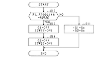
- FIG. 4 is a flowchart showing a processing procedure of the break circuit.
- FIG. 5 is a time chart showing an example of the overcurrent protection operation.
- FIG. 6 is a time chart showing an example of the overcurrent protection operation.
- FIG. 7 is a time chart showing an example of the overcurrent protection operation according to Comparative Example 1.
- FIG. 8 is a time chart showing an example of the overcurrent protection operation according to Comparative Example 2.
- FIG. 9 is a flowchart showing a processing procedure of the break circuit according to the second embodiment.
- FIG. 10 is a flowchart showing a processing procedure of the break circuit according to the third embodiment.
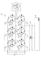
- the control system includes a DC power supply 10, an inverter 20, a rotating electric machine 30, and a control device 40.
- the rotary electric machine 30 is, for example, an in-vehicle main engine.
- the rotary electric machine 30 is electrically connected to the DC power supply 10 via the inverter 20.
- a three-phase rotary electric machine 30 is used.
- the rotary electric machine 30, for example, a permanent magnet synchronous machine can be used.
- the DC power supply 10 is a storage battery having a terminal voltage of, for example, 100 V or more.
- the DC power supply 10 is, for example, a secondary battery such as a lithium ion storage battery or a nickel hydrogen storage battery.
- a capacitor 11 is connected in parallel to the DC power supply 10.
- the inverter 20 is provided with upper and lower arm switch portions 20H and 20L corresponding to each phase.
- the upper arm switch unit 20H and the lower arm switch unit 20L are connected in series.
- the first end of the winding 31 of the rotary electric machine 30 is connected to the connection point between the upper arm switch unit 20H and the lower arm switch unit 20L.
- the second end of the winding 31 of each phase is connected at a neutral point.
- Each of the switch units 20H and 20L includes a parallel connection body of the first switch SW1 and the second switch SW2.
- the positive electrode side of the DC power supply 10 is connected to the high potential side terminals of the first switch SW1 and the second switch SW2 of the upper arm switch unit 20H.
- the negative side of the DC power supply 10 is connected to the low potential side terminals of the first switch SW1 and the second switch SW2 of the lower arm switch section 20L.
- the high potential side terminals of the first switch SW1 and the second switch SW2 of the lower arm switch section 20L are connected to the low potential side terminals of the first switch SW1 and the second switch SW2 of the upper arm switch section 20H, respectively. It is connected.
- the first switch SW1 is an N-channel MOSFET as a SiC device. Therefore, in the first switch SW1, the low potential side terminal is the source and the high potential side terminal is the drain.
- the second switch SW2 is an IGBT as a Si device. Therefore, in the second switch SW2, the low potential side terminal is the emitter and the high potential side terminal is the collector.
- a freewheel diode is connected in antiparallel to the second switch SW2, and a body diode is formed in the first switch SW1.
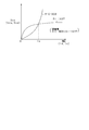
- FIG. 2 is a diagram showing the relationship between the current flowing through the switch and the voltage Von between the high and low potential side terminals of the switch. Specifically, FIG. 2 shows the voltage-current characteristics of the drain-source voltage Vds and the drain current Id of the MOSFET, and the voltage-current characteristics of the collector-emitter voltage Vce and the collector current Ic of the IGBT.
- the drain-source voltage Vds for the drain current Id is lower than the collector-emitter voltage Vce for the collector current Ic. That is, in the small current region, the on resistance of the MOSFET is smaller than the on resistance of the IGBT. Therefore, in the small current region, a large amount of current flows in the MOSFET among the MOSFET and the IGBT connected in parallel with each other.
- the collector-emitter voltage Vce with respect to the collector current Ic is lower than the drain-source voltage Vds with respect to the drain current Id.
- the on-resistance of the IGBT is smaller than the on-resistance of the MOSFET. Therefore, in the large current region, a large amount of current flows in the IGBT among the MOSFET and the IGBT connected in parallel with each other.
- the short-circuit tolerance of the first switch SW1 is lower than the short-circuit tolerance of the second switch SW2.
- the short circuit withstand capability is the time from when the overcurrent starts flowing through the first switch SW1 to when the first switch SW1 is destroyed, or after the overcurrent starts flowing through the first switch SW1. It is energy (specifically, current ⁇ voltage time integrated value) generated in the first switch SW1 until the destruction of the first switch SW1.
- the rated current of the drain current of the first switch SW1 is smaller than the rated current of the collector current of the second switch SW2, for example.
- the control device 40 drives the inverter 20 to control the control amount of the rotating electric machine 30 to the command value.
- the control amount is, for example, torque.
- the control device 40 drives the drive signals Gc corresponding to the switches SW1 and SW2 to drive the switches SW1 and SW2 of the inverter 20 to the drive circuits 50 individually provided to the switch units 20H and 20L. Output to.
- the control device 40 generates the drive signal Gc corresponding to each drive circuit 50, for example, by the PWM processing based on the magnitude comparison of the three-phase command voltage and the carrier signal such as a triangular wave whose phases are different from each other by 120° in electrical angle. ..
- the drive signal Gc takes either an on command for instructing on driving of the switch or an off command for instructing off driving.
- the drive signal on the upper arm side and the corresponding drive signal on the lower arm side are alternately turned on commands. Therefore, in each phase, the switch of the upper arm switch unit 20H and the switch of the lower arm switch unit 20L are alternately turned on.
- the control system includes a break circuit 60.
- the cutoff circuit 60 divides the drive signal Gc output from the control device 40 into a first drive signal G1 corresponding to the first switch SW1 and a second drive signal G2 corresponding to the second switch SW2, and the drive circuit Output to 50.
- the control device 40 and the cutoff circuit 60 are provided in the low voltage system, and the drive circuit 50 is provided in the high voltage system electrically insulated from the low voltage system.
- the signal exchange between the cutoff circuit 60 and the drive circuit 50 is, for example, an optical insulation element (for example, a photocoupler) or magnetic insulation capable of transmitting a signal while electrically insulating between the low voltage system and the high voltage system. It may be carried out using an element (for example, a magnetic coupler).
- control device 40 the drive circuit 50, and the break circuit 60 may be provided by, for example, software recorded in a physical memory device and a computer, hardware, or a combination thereof that executes the software. it can.
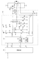
- the drive circuit 50 includes a first charging switch 70, a first constant voltage power source 71, a first charging resistor 72, and a first balance resistor 73.
- a P-channel MOSFET is used as the first charging switch 70.
- the first constant voltage power supply 71 is connected to the source of the first charging switch 70, and the first end of the first charging resistor 72 is connected to the drain of the first charging switch 70.
- the first end of the first balance resistor 73 is connected to the second end of the first charging resistor 72.
- the gate of the first switch SW1 is connected to the second end of the first balance resistor 73.
- the drive circuit 50 includes a first discharge resistor 74, a first discharge switch 75, a first protection resistor 76, a first protection switch 77, and a first off holding switch 78.
- N-channel MOSFETs are used as the first discharge switch 75, the first protection switch 77, and the first off-hold switch 78.
- the drain of the first discharge switch 75 is connected to the first end of the first balance resistor 73 via the first discharge resistor 74.
- the source of the first switch SW1 is connected to the source of the first discharge switch 75.
- the drain of the first protection switch 77 is connected to the first end of the first balance resistor 73 via the first protection resistor 76.
- the source of the first switch SW1 is connected to the source of the first protection switch 77.
- the drain of the first off holding switch 78 is connected to the gate of the first switch SW1.
- the source of the first switch SW1 is connected to the source of the first off holding switch 78.
- the drive circuit 50 includes a second charging switch 80, a second constant voltage power supply 81, a second charging resistor 82, and a second balance resistor 83.
- a P-channel MOSFET is used as the second charging switch 80.
- a second constant voltage power supply 81 is connected to the source of the second charging switch 80, and the first end of the second charging resistor 82 is connected to the drain of the second charging switch 80.
- the first end of the second balance resistor 83 is connected to the second end of the second charging resistor 82.
- the gate of the second switch SW2 is connected to the second end of the second balance resistor 83.
- the output voltage of the second constant voltage power supply 81 is set lower than the output voltage of the first constant voltage power supply 71. However, this setting is not mandatory.
- the drive circuit 50 includes a second discharge resistor 84, a second discharge switch 85, a second protection resistor 86 as a soft cutoff resistor, a second protection switch 87, and a second off holding switch 88.
- N-channel MOSFETs are used as the second discharge switch 85, the second protection switch 87, and the second off-holding switch 88.
- the emitter of the second switch SW2 is connected to the first end of the second balance resistor 83 via the second discharge resistor 84 and the second discharge switch 85.
- the emitter of the second switch SW2 is connected to the first end of the second balance resistor 83 via the second protection resistor 86 and the second protection switch 87.
- the gate of the second switch SW2 is connected to the emitter of the second switch SW2 via the second off holding switch 88.
- the first switch SW1 includes a first sense terminal St1.
- the first sense terminal St1 outputs a minute current having a correlation with the drain current of the first switch SW1.
- the first end of the first sense resistor 79 of the drive circuit 50 is connected to the first sense terminal St1, and the source of the first switch SW1 is connected to the second end of the first sense resistor 79. ..
- a voltage drop occurs in the first sense resistor 79 due to the minute current flowing through the first sense terminal St1. Therefore, the voltage drop amount of the first sense resistor 79 can be used as the correlation value of the drain current.
- the potential difference of the first sense resistor 79 is input to the drive control unit 90 of the drive circuit 50 as the first sense voltage Vse1. In the present embodiment, among both ends of the first sense resistor 79, the first sense voltage Vse1 when the potential of the first end is higher than that of the second end is defined as positive.
- the second switch SW2 is provided with a second sense terminal St2.
- the second sense terminal St2 outputs a minute current having a correlation with the collector current of the second switch SW2.
- the first end of the second sense resistor 89 of the drive circuit 50 is connected to the second sense terminal St2, and the emitter of the second switch SW2 is connected to the second end of the second sense resistor 89. ..
- the potential difference of the second sense resistor 89 is input to the drive control unit 90 as the second sense voltage Vse2.
- the second sense voltage Vse2 when the potential of the first end is higher than that of the second end is defined as positive.
- the drive control unit 90 drives the first and second switches SW1 and SW2 on and off based on the first and second drive signals G1 and G2 output from the cutoff circuit 60. Specifically, when the drive control unit 90 determines that the first drive signal G1 is on command, the drive control unit 90 drives the first charge switch 70 on and drives the first discharge switch 75 off. As a result, a charging current flows from the first constant voltage power supply 71 to the gate of the first switch SW1, and the gate voltage of the first switch SW1 becomes equal to or higher than the first threshold voltage Vth1. As a result, the first switch SW1 is switched from the off state to the on state.
- the drive control unit 90 determines that the first drive signal G1 is an off command
- the drive control unit 90 sets the first charge switch 70 to off drive and drives the first discharge switch 75 on.
- a discharge current flows from the gate of the first switch SW1 to the source, and the gate voltage of the first switch SW1 becomes less than the first threshold voltage Vth1.
- the first switch SW1 is switched from the on state to the off state.
- the drive control unit 90 determines that the second drive signal G2 is on command, the drive control unit 90 drives the second charge switch 80 on and drives the second discharge switch 85 off. As a result, a charging current flows from the second constant voltage power supply 81 to the gate of the second switch SW2, and the gate voltage of the second switch SW2 becomes the second threshold voltage Vth2 or more. As a result, the second switch SW2 is switched from the off state to the on state.
- the drive control unit 90 determines that the second drive signal G2 is an off command
- the drive control unit 90 sets the second charge switch 80 to off drive and drives the second discharge switch 85 on.
- a discharge current flows from the gate of the second switch SW2 to the emitter, and the gate voltage of the second switch SW2 becomes less than the second threshold voltage Vth2.
- the second switch SW2 is switched from the on state to the off state.
- the drive control unit 90 performs the off holding process. Specifically, the drive controller 90 has a function of detecting the gate voltage of the first and second switches SW1 and SW2. The drive control unit 90 drives the first off holding switch 78 based on the first drive signal G1 output from the cutoff circuit 60 and the detected gate voltage of the first switch SW1, and is output from the cutoff circuit 60. Based on the second drive signal G2 and the detected gate voltage of the second switch SW2, the off-holding process for driving the second off-holding switch 88 is performed.
- the drive control unit 90 determines that the first drive signal G1 is an off command and the gate voltage of the first switch SW1 is equal to or less than the first specified voltage V ⁇ 1, the first The off-holding switch 78 is driven on, and the first off-holding switch 78 is driven off in other cases.
- the first specified voltage V ⁇ 1 is set to a voltage equal to or lower than the first threshold voltage Vth1.
- the second off holding switch 88 is turned on, and in other cases, the second off holding switch 88 is turned off.
- the second specified voltage V ⁇ 2 is set to a voltage equal to or lower than the second threshold voltage Vth2.
- the drive control unit 90 includes a first short circuit determination unit 91 and a second short circuit determination unit 92 (corresponding to a “determination unit”).
- the first and second short circuit determination units 91 and 92 are provided to determine whether or not an overcurrent (short circuit current) is flowing through the first and second switches SW1 and SW2.
- the first short-circuit determination unit 91 determines that the input first sense voltage Vse1 exceeds the first determination threshold Voc1, it outputs the first fail signal F1 notifying that an overcurrent is flowing to the first switch SW1. Output to the cutoff circuit 60.
- the first short-circuit determination unit 91 determines that the first sense voltage Vse1 has become equal to or lower than the first release threshold Vjdg1 smaller than the first determination threshold Voc1 after starting to output the first fail signal F1, The output of the fail signal F1 is stopped.
- the first release threshold Vjdg1 is set to a value slightly larger than 0 or 0.
- the second short circuit determination unit 92 determines that the input second sense voltage Vse2 exceeds the second determination threshold Voc2, it outputs the second fail signal F2 notifying that the overcurrent is flowing to the second switch SW2. Output to the cutoff circuit 60.
- the second short circuit determination unit 92 determines that the second sense voltage Vse2 has become equal to or lower than the second release threshold Vjdg2 after starting to output the second fail signal F2, the second short circuit determination unit 92 stops the output of the second fail signal F2.
- the second release threshold Vjdg2 is set to a value slightly larger than 0 or 0. Note that the overcurrent is caused by upper and lower arm short circuits, interphase short circuits, ground faults, and the like.
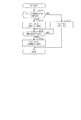
- step S10 it is determined whether at least one of the first fail signal F1 and the second fail signal F2 is input.
- step S10 When a negative determination is made in step S10, it is determined that an overcurrent does not flow in any of the first and second switches SW1 and SW2, and the process proceeds to step S11.
- step S11 the drive signal Gc input from the control device 40 is output to the drive control unit 90 as the first and second drive signals G1 and G2. That is, when the drive signal Gc is an on command, the first and second drive signals G1 and G2 of the on command are output, and when the drive signal Gc is an off command, the first and second drive signals G1 and G2 of the off command are output. Is output.
- step S10 If an affirmative decision is made in step S10, it is decided that an overcurrent is flowing in at least one of the first and second switches SW1, SW2, and the operation proceeds to step S12.
- step S12 the first drive signal G1 output to the drive controller 90 is turned off regardless of the input drive signal Gc. In this case, when the input first drive signal G1 is switched to the off command while the drive control unit 90 is outputting at least one of the first and second fail signals F1 and F2, the first charge switch 70, the first discharge switch 75 and the first off holding switch 78 are turned off, and the first protection switch 77 is turned on.
- the resistance value of the first protection switch 77 is Rs1
- the resistance value of the first balance resistor 73 is Rb1
- the resistance value of the second protection switch 87 is Rs2
- the resistance value of the second balance resistor 83 is Rs1.
- the value is Rb2.
- "Rs1 + Rb1 ⁇ Rs2 + Rb2" is set. With this setting, the switching speed when the first switch SW1 is switched to the off state is higher than the switching speed when the second switch SW2 is switched to the off state in the process of step S14 described later.
- step S13 it is determined whether or not the switching of the first switch SW1 to the off state is completed.
- the first sense voltage Vse1 becomes equal to or less than the first release threshold value Vjdg1 and the input of the first fail signal F1 is stopped, it is determined that the switching is completed.
- step S13 If an affirmative determination is made in step S13, the process proceeds to step S14, and the second drive signal G2 output to the drive control unit 90 is turned off regardless of the input drive signal Gc.
- the drive control unit 90 drives the second charge switch 80, the second discharge switch 85, and the second off holding switch 88 off, and drives the second protection switch 87 on.
- the second switch SW2 is switched to the off state at a switching speed lower than the switching speed when the first switch SW1 is switched to the off state.
- the cutoff circuit 60 constitutes an overcurrent protection unit.
- the overcurrent protection operation by the breaking circuit 60 when the upper and lower arm short circuits occur will be described with reference to FIGS. 5 and 6.
- the upper and lower arm switch portions 20H and 20L one is an opposing arm and the other is an own arm, and an overcurrent protection operation by the cutoff circuit 60 of the own arm will be described.
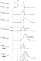
- FIG. 5 describes a case where the first and second switches SW1 and SW2 of the own arm are turned on while at least one of the first and second switches SW1 and SW2 of the opposite arm is short-circuited.
- 5 (a) and 5 (b) show the transition of the first and second drive signals G1 and G2 output from the breaking circuit 60
- FIG. 5 (c) shows the gate voltage Vgs (gate) of the first switch SW1.
- 5D shows the transition of the gate voltage Vge (gate-emitter voltage) of the second switch SW2.
- 5E and 5F show changes in the first and second sense voltages Vse1 and Vse2, and
- the first and second drive signals G1 and G2 output from the cutoff circuit 60 to the drive control unit 90 are switched to the ON command.
- the gate voltage Vgs of the first switch SW1 and the gate voltage Vge of the second switch SW2 start to rise.
- the first sense voltage Vse1 exceeds the first determination threshold value Voc1. Therefore, the first fail signal F1 is output from the first short circuit determination unit 91 to the cutoff circuit 60, and the first drive signal G1 output from the cutoff circuit 60 to the drive control unit 90 is switched to the off command. .. As a result, at time t4, the gate voltage Vgs of the first switch SW1 starts to decrease.
- the first sense voltage Vse1 becomes equal to or lower than the first release threshold Vjdg1. Therefore, the output of the first fail signal F1 from the first short circuit determination unit 91 to the cutoff circuit 60 is stopped, and the second drive signal G2 output from the cutoff circuit 60 to the drive control unit 90 is switched to the off command. .. As a result, at time t6, the gate voltage Vge of the second switch SW2 starts to decrease.
- the decreasing speed ⁇ dVmos of the first sense voltage Vse1 when the first switch SW1 is switched to the off state is higher than the decreasing speed ⁇ dVigbt of the second sense voltage Vse2 when the second switch SW2 is switched to the off state. .. That is, the switching speed when the first switch SW1 is switched to the off state is higher than the switching speed when the second switch SW2 is switched to the off state.
- the time for the overcurrent to flow through the first switch SW1 can be shortened, and the time integral value (energy) of the loss generated in the first switch SW1 can be set to be equal to or less than the short-circuit tolerance of the first switch SW1.
- FIG. 5 shows an example in which the first switch SW1 is switched to the off state first when it is determined that an overcurrent has flowed through the first switch SW1, but it is determined that an overcurrent has flowed through the second switch SW2. Also, the first switch SW1 is switched to the off state first.
- FIG. 6 describes a case where at least one of the first and second switches SW1 and SW2 of the opposite arm fails in a short circuit while the first and second switches SW1 and SW2 of the own arm are driven on.
- FIGS. 6(a) to 6(h) correspond to FIGS. 5(a) to 5(h).
- the first and second drive signals G1 and G2 output from the cutoff circuit 60 to the drive control unit 90 are switched to the ON command.
- the gate voltage Vgs of the first switch SW1 and the gate voltage Vge of the second switch SW2 start to rise.
- the first sense voltage Vse1 exceeds the first determination threshold Voc1. Therefore, the first fail signal F1 is output from the first short circuit determination unit 91 to the cutoff circuit 60, and the first drive signal G1 output from the cutoff circuit 60 to the drive control unit 90 is switched to the off command. .. As a result, at time t4, the gate voltage Vgs of the first switch SW1 starts to decrease.
- the first sense voltage Vse1 becomes equal to or lower than the first release threshold Vjdg1. Therefore, the output of the first fail signal F1 from the first short circuit determination unit 91 to the cutoff circuit 60 is stopped, and the second drive signal G2 output from the cutoff circuit 60 to the drive control unit 90 is switched to the off command. .. As a result, the gate voltage Vge of the second switch SW2 begins to decrease.
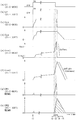
- FIG. 7 shows a case where the first and second switches SW1 and SW2 of the own arm are turned on while at least one of the first and second switches SW1 and SW2 of the opposing arm is short-circuited.
- FIGS. 7(a) to 7(h) correspond to the previous FIGS. 5(a) to 5(h).
- the first and second drive signals G1 and G2 output from the cutoff circuit 60 to the drive control unit 90 are switched to the ON command.
- the gate voltage Vgs of the first switch SW1 and the gate voltage Vge of the second switch SW2 start to rise.
- the cutoff circuit 60 when at least one of the first and second fail signals F1 and F2 is input to the cutoff circuit 60, the cutoff circuit 60 simultaneously switches the first and second drive signals G1 and G2 to the off command. Specifically, at time t3, the first sense voltage Vse1 exceeds the first determination threshold value Voc1. Therefore, the first fail signal F1 is output from the first short circuit determination unit 91 to the cutoff circuit 60, and the first and second drive signals G1 and G2 output from the cutoff circuit 60 to the drive control unit 90 are output. Switched to off command. As a result, at time t4, the gate voltage Vgs of the first switch SW1 and the gate voltage Vge of the second switch SW2 start to decrease.
- FIG. 8 shows a case where the first and second switches SW1 and SW2 of the own arm are turned on while at least one of the first and second switches SW1 and SW2 of the opposing arm is short-circuited.
- 8 (a) to 8 (f) correspond to the above FIGS. 5 (a) to 5 (f)
- FIG. 8 (g) shows the transition of the phase current flowing through the winding 31.
- times t1 to t4 in FIG. 8 correspond to times t1 to t4 in FIG.
- Comparative Example 2 when at least one of the first and second fail signals F1 and F2 is input to the cutoff circuit 60, the cutoff circuit 60 has the first and second drive signals G1 and G2 as in Comparative Example 1. Are simultaneously switched to the off command. Further, in Comparative Example 2, the switching speed when the second switch SW2 is switched to the off state is set in two ways. In FIGS. 8D and 8G, the case where the switching speed is low is shown by the broken line, and the case where the switching speed is high is shown by the solid line.
- the first switch SW1 When it is determined that an overcurrent has flowed to at least one of the first and second switches SW1 and SW2, the first switch SW1 having a smaller short-circuit tolerance among the first and second switches SW1 and SW2 is switched from the second switch SW2. Also switched to the off state first. As a result, the time during which the overcurrent flows through the first switch SW1 can be shortened, and the energy generated by the first switch SW1 can be made equal to or less than the short-circuit tolerance of the first switch SW1. As a result, the first switch SW1 can be appropriately protected from overcurrent.
- the first switch SW1 that can be switched to the off state first does not generate a large surge voltage due to the switching to the off state. Therefore, the switching speed of the first switch SW1 that is not finally turned off can be higher than that of the second switch SW2 that is finally turned off. In view of this point, the switching speed of the first switch SW1 is set higher than the switching speed of the second switch SW2. Thereby, when switching to the off state, the flow time of the overcurrent of the first switch SW1 can be shortened, and the energy generated in the first switch SW1 can be further reduced.
- the first switch SW1 When it was determined that an overcurrent had flowed to any one of the first and second switches SW1 and SW2, the first switch SW1 was first switched to the off state. As a result, even when it is determined that the overcurrent flows through the second switch SW2, it is possible to quickly shift to the overcurrent protection operation of the first switch SW1.
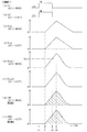
- FIG. 9 shows a procedure of processing executed by the break circuit 60.
- the same processes as those shown in FIG. 4 above are given the same reference numerals for convenience.
- step S14 is performed before the switching of the first switch SW1 to the off state is completed. Even in this case, it is possible to obtain an effect similar to the effect of the first embodiment.
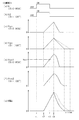
- FIG. 10 shows a procedure of processing executed by the break circuit 60.
- the same processes as those shown in FIG. 4 above are designated by the same reference numerals for convenience.
- the first protection resistor 76 and the first protection switch 77 are not provided in the configuration of FIG. 3 described above.
- step S10 the process proceeds to step S15.
- step S15 the first drive signal G1 output to the drive control unit 90 is turned off regardless of the input drive signal Gc.
- the drive control unit 90 switches the first charge switch when the input first drive signal G1 is switched to the off command while at least one of the first and second fail signals F1 and F2 is being output. 70, the first discharge switch 75 and the first off holding switch 78 are turned off, and the first off holding switch 78 is turned on.
- the first switch SW1 is switched to the off state by using the first off holding switch 78. According to this configuration, the switching speed when the first off holding switch 78 is switched to the off state can be further increased, and the energy generated by the first switch SW1 can be further reduced.
- the first off holding switch 78 can be diverted as the switch used in the overcurrent protection operation, and it is not necessary to provide the first protection resistor 76 and the first protection switch 77 in the drive circuit 50. Therefore, the number of parts of the drive circuit 50 can be reduced.
- the number of switches composing the switch section of each arm of each phase may be three or more.
- the first switch, the second switch, and the third switch are arranged in order of increasing short circuit withstand capability.
- the first switch among the first to third switches is first switched to the off state, and then the second switch is turned off. It suffices if it is switched to and finally the third switch is switched to the off state.
- the switches that make up the switch section of each arm of each phase are not limited to the same type of switch.
- the first and second switches are MOSFETs configured of SiC devices, the short circuit capacitance may differ due to the difference in chip size. Even in such cases, the application of the present disclosure is valid.
- the drive control unit 90 may have the function of the cutoff circuit 60 without providing the cutoff circuit 60 in the control system.
- the power conversion circuit is not limited to an inverter, and may be, for example, a full bridge circuit as long as it has upper and lower arm switches.
- control unit and its method described in the present disclosure are realized by a dedicated computer provided by configuring a processor and a memory programmed to execute one or more functions embodied by a computer program. May be done.
- control unit and the method described in the present disclosure may be realized by a dedicated computer provided by configuring a processor with one or more dedicated hardware logic circuits.
- control unit and the method thereof described in the present disclosure are based on a combination of a processor and a memory programmed to execute one or a plurality of functions and a processor configured by one or more hardware logic circuits. It may be realized by one or more dedicated computers configured.
- the computer program may be stored in a computer-readable non-transitional tangible recording medium as an instruction executed by the computer.
Abstract
This drive device performs a drive control on a plurality of switches (SW1, SW2) connected in parallel with each other. The plurality of switches include switches having different short circuit capacities. The drive device comprises: determination units (91, 92) that determine whether or not an overcurrent flows in at least one of the plurality of switches; and an overcurrent protection unit (60) that switches the plurality of switches to an OFF state when the determination units determine that the overcurrent has flowed. The overcurrent protection unit firstly switches, to the OFF state, a minimum short circuit capacity switch (SW1), which is a switch having the smallest short circuit capacity, among the plurality of switches.
Description
本出願は、2019年3月1日に出願された日本出願番号2019-038050号に基づくもので、ここにその記載内容を援用する。
This application is based on Japanese application No. 2019-038050 filed on Mar. 1, 2019, and the content of the description is incorporated herein.
本開示は、スイッチの駆動装置に関する。
This disclosure relates to a switch drive device.
従来、例えば特許文献1に記載されているように、Siデバイスで構成されるIGBTを駆動する駆動装置が知られている。この駆動装置は、IGBTに過電流が流れたと判定した場合、IGBTをオフ状態に切り替えることにより、IGBTの保護を図っている。
Conventionally, as described in Patent Document 1, for example, a drive device for driving an IGBT composed of Si devices is known. This drive device protects the IGBT by switching the IGBT to the off state when it is determined that an overcurrent has flowed to the IGBT.
駆動装置としては、IGBTと、IGBTに並列接続され、SiCデバイスで構成されたMOSFETとを駆動するものもある。ここで、MOSFETの短絡耐量は、IGBTの短絡耐量よりも低い。このため、MOSFET及びIGBTの並列接続体に過電流が流れる場合において、短絡耐量が低いMOSFETを適切に保護できる技術が望まれる。
As a driving device, there is also a driving device that drives an IGBT and a MOSFET that is connected in parallel to the IGBT and is composed of a SiC device. Here, the short-circuit withstand capability of the MOSFET is lower than the short-circuit withstand capability of the IGBT. Therefore, there is a demand for a technique capable of appropriately protecting a MOSFET having a low short circuit resistance when an overcurrent flows in a parallel connection body of the MOSFET and the IGBT.
なお、互いに並列接続されたMOSFET及びIGBTに限らず、互いに並列接続された複数のスイッチであって、異なる短絡耐量を有するスイッチが含まれる複数のスイッチを過電流から適切に保護できる技術が望まれる。
It should be noted that a technique capable of appropriately protecting a plurality of switches connected in parallel with each other, including switches having different short-circuit tolerances, is desired, not limited to MOSFETs and IGBTs connected in parallel with each other. ..
本開示は、互いに並列接続された複数のスイッチのうち短絡耐量が最も小さいスイッチを過電流から適切に保護できるスイッチの駆動装置を提供することを主たる目的とする。
The main object of the present disclosure is to provide a switch drive device capable of appropriately protecting a switch having the smallest short-circuit tolerance among a plurality of switches connected in parallel with each other from overcurrent.
本開示は、互いに並列接続された複数のスイッチの駆動制御を行うスイッチの駆動装置において、
複数の前記スイッチには、異なる短絡耐量を有するスイッチが含まれており、
複数の前記スイッチの少なくとも1つに過電流が流れたことを判定する判定部と、
前記判定部により過電流が流れたと判定された場合、複数の前記スイッチをオフ状態に切り替える過電流保護部と、を備え、
前記過電流保護部は、複数の前記スイッチのうち、短絡耐量が最も小さいスイッチである最小耐量スイッチを最初にオフ状態に切り替える。 The present disclosure relates to a switch drive device that controls drive of a plurality of switches connected in parallel to each other.
The plurality of said switches include switches having different short circuit tolerances.
A determination unit that determines that an overcurrent has flowed through at least one of the plurality of switches,
When it is determined by the determination unit that an overcurrent has flowed, an overcurrent protection unit for switching a plurality of the switches to an off state is provided.
The overcurrent protection unit first switches the minimum withstand voltage switch, which is the switch with the smallest short circuit withstand capability, to the off state among the plurality of the switches.
本開示では、複数のスイッチのうち最小耐量スイッチを最初にオフ状態に切り替えるため、最小耐量スイッチに過電流が流れる時間を短縮することができる。これにより、過電流が流れたと判定されてから最小耐量スイッチがオフ状態に切り替えられるまでに最小耐量スイッチで発生するエネルギを低減でき、そのエネルギを最小耐量スイッチの短絡耐量以下にできる。その結果、最小耐量スイッチを過電流から適切に保護することができる。
In the present disclosure, the minimum withstand voltage switch of the plurality of switches is first switched to the OFF state, so that the time during which an overcurrent flows through the minimum withstand voltage switch can be shortened. As a result, the energy generated by the minimum withstand voltage switch from the time when it is determined that the overcurrent has flowed until the minimum withstand voltage switch is switched to the off state can be reduced, and the energy can be made equal to or less than the short circuit withstand capability of the minimum withstand voltage switch. As a result, the minimum withstand voltage switch can be adequately protected from overcurrent.
本開示についての上記目的およびその他の目的、特徴や利点は、添付の図面を参照しながら下記の詳細な記述により、より明確になる。その図面は、
図1は、第1実施形態に係る制御システムの全体構成図であり、
図2は、第1,第2スイッチの電流電圧特性を示す図であり、
図3は、駆動回路及びその周辺構成を示す図であり、
図4は、遮断回路の処理手順を示すフローチャートであり、
図5は、過電流保護動作の一例を示すタイムチャートであり、
図6は、過電流保護動作の一例を示すタイムチャートであり、
図7は、比較例1に係る過電流保護動作の一例を示すタイムチャートであり、
図8は、比較例2に係る過電流保護動作の一例を示すタイムチャートであり、
図9は、第2実施形態に係る遮断回路の処理手順を示すフローチャートであり、
図10は、第3実施形態に係る遮断回路の処理手順を示すフローチャートである。
The above objectives and other objectives, features and advantages of the present disclosure will be clarified by the following detailed description with reference to the accompanying drawings. The drawing is
FIG. 1 is an overall configuration diagram of the control system according to the first embodiment. FIG. 2 is a diagram showing the current-voltage characteristics of the first and second switches. FIG. 3 is a diagram showing a drive circuit and its peripheral configuration. FIG. 4 is a flowchart showing a processing procedure of the break circuit. FIG. 5 is a time chart showing an example of the overcurrent protection operation. FIG. 6 is a time chart showing an example of the overcurrent protection operation. FIG. 7 is a time chart showing an example of the overcurrent protection operation according to Comparative Example 1. FIG. 8 is a time chart showing an example of the overcurrent protection operation according to Comparative Example 2. FIG. 9 is a flowchart showing a processing procedure of the break circuit according to the second embodiment. FIG. 10 is a flowchart showing a processing procedure of the break circuit according to the third embodiment.
<第1実施形態>
以下、本開示に係る駆動装置を具体化した第1実施形態について、図面を参照しつつ説明する。 <First Embodiment>
Hereinafter, the first embodiment in which the drive device according to the present disclosure is embodied will be described with reference to the drawings.
以下、本開示に係る駆動装置を具体化した第1実施形態について、図面を参照しつつ説明する。 <First Embodiment>
Hereinafter, the first embodiment in which the drive device according to the present disclosure is embodied will be described with reference to the drawings.
図1に示すように、制御システムは、直流電源10、インバータ20、回転電機30及び制御装置40を備えている。回転電機30は、例えば車載主機である。回転電機30は、インバータ20を介して直流電源10に電気的に接続されている。本実施形態では、回転電機30として、3相のものが用いられている。回転電機30としては、例えば、永久磁石同期機を用いることができる。また、直流電源10は、例えば百V以上となる端子電圧を有する蓄電池である。直流電源10は、例えば、リチウムイオン蓄電池やニッケル水素蓄電池等の2次電池である。なお、直流電源10には、コンデンサ11が並列接続されている。
As shown in FIG. 1, the control system includes a DC power supply 10, an inverter 20, a rotating electric machine 30, and a control device 40. The rotary electric machine 30 is, for example, an in-vehicle main engine. The rotary electric machine 30 is electrically connected to the DC power supply 10 via the inverter 20. In this embodiment, a three-phase rotary electric machine 30 is used. As the rotary electric machine 30, for example, a permanent magnet synchronous machine can be used. Further, the DC power supply 10 is a storage battery having a terminal voltage of, for example, 100 V or more. The DC power supply 10 is, for example, a secondary battery such as a lithium ion storage battery or a nickel hydrogen storage battery. A capacitor 11 is connected in parallel to the DC power supply 10.
インバータ20は、各相に対応する上,下アームスイッチ部20H,20Lを備えている。各相において、上アームスイッチ部20Hと下アームスイッチ部20Lとは直列接続されている。各相において、上アームスイッチ部20Hと下アームスイッチ部20Lとの接続点には、回転電機30の巻線31の第1端が接続されている。各相の巻線31の第2端は、中性点で接続されている。
The inverter 20 is provided with upper and lower arm switch portions 20H and 20L corresponding to each phase. In each phase, the upper arm switch unit 20H and the lower arm switch unit 20L are connected in series. In each phase, the first end of the winding 31 of the rotary electric machine 30 is connected to the connection point between the upper arm switch unit 20H and the lower arm switch unit 20L. The second end of the winding 31 of each phase is connected at a neutral point.
各スイッチ部20H,20Lは、第1スイッチSW1及び第2スイッチSW2の並列接続体を備えている。各相において、上アームスイッチ部20Hの第1スイッチSW1及び第2スイッチSW2それぞれの高電位側端子には、直流電源10の正極側が接続されている。各相において、下アームスイッチ部20Lの第1スイッチSW1及び第2スイッチSW2それぞれの低電位側端子には、直流電源10の負極側が接続されている。各相において、上アームスイッチ部20Hの第1スイッチSW1及び第2スイッチSW2それぞれの低電位側端子には、下アームスイッチ部20Lの第1スイッチSW1及び第2スイッチSW2それぞれの高電位側端子が接続されている。
Each of the switch units 20H and 20L includes a parallel connection body of the first switch SW1 and the second switch SW2. In each phase, the positive electrode side of the DC power supply 10 is connected to the high potential side terminals of the first switch SW1 and the second switch SW2 of the upper arm switch unit 20H. In each phase, the negative side of the DC power supply 10 is connected to the low potential side terminals of the first switch SW1 and the second switch SW2 of the lower arm switch section 20L. In each phase, the high potential side terminals of the first switch SW1 and the second switch SW2 of the lower arm switch section 20L are connected to the low potential side terminals of the first switch SW1 and the second switch SW2 of the upper arm switch section 20H, respectively. It is connected.
本実施形態において、第1スイッチSW1は、SiCデバイスとしてのNチャネルMOSFETである。このため、第1スイッチSW1において、低電位側端子はソースであり、高電位側端子はドレインである。また、第2スイッチSW2は、SiデバイスとしてのIGBTである。このため、第2スイッチSW2において、低電位側端子はエミッタであり、高電位側端子はコレクタである。なお、第2スイッチSW2には、フリーホイールダイオードが逆並列に接続されており、第1スイッチSW1には、ボディダイオードが形成されている。
In the present embodiment, the first switch SW1 is an N-channel MOSFET as a SiC device. Therefore, in the first switch SW1, the low potential side terminal is the source and the high potential side terminal is the drain. The second switch SW2 is an IGBT as a Si device. Therefore, in the second switch SW2, the low potential side terminal is the emitter and the high potential side terminal is the collector. A freewheel diode is connected in antiparallel to the second switch SW2, and a body diode is formed in the first switch SW1.
各スイッチ部20H,20LをIGBT及びMOSFETの並列接続体で構成した理由は、小電流領域においてオン抵抗が低いMOSFETの方に電流を多く流通させることにより、小電流領域における損失を低減するためである。以下、損失低減について、図2を用いて説明する。図2は、スイッチに流れる電流とスイッチの高,低電位側端子間の電圧Vonとの関係を示す図である。詳しくは、図2は、MOSFETのドレイン及びソース間電圧Vdsとドレイン電流Idとの電圧電流特性、並びにIGBTのコレクタ及びエミッタ間電圧Vceとコレクタ電流Icとの電圧電流特性を示す。
The reason why each of the switch units 20H and 20L is configured by the parallel connection body of the IGBT and the MOSFET is to reduce the loss in the small current region by allowing more current to flow in the MOSFET having a lower ON resistance in the small current region. is there. Hereinafter, loss reduction will be described with reference to FIG. FIG. 2 is a diagram showing the relationship between the current flowing through the switch and the voltage Von between the high and low potential side terminals of the switch. Specifically, FIG. 2 shows the voltage-current characteristics of the drain-source voltage Vds and the drain current Id of the MOSFET, and the voltage-current characteristics of the collector-emitter voltage Vce and the collector current Ic of the IGBT.
図2に示すように、電流が所定電流Iαよりも小さい小電流領域においては、ドレイン電流Idに対するドレイン及びソース間電圧Vdsが、コレクタ電流Icに対するコレクタ及びエミッタ間電圧Vceよりも低い。すなわち、小電流領域においては、MOSFETのオン抵抗がIGBTのオン抵抗よりも小さい。このため、小電流領域においては、互いに並列接続されたMOSFET及びIGBTのうち、MOSFETの方に電流が多く流れることとなる。一方、電流が所定電流Iαよりも大きい大電流領域においては、コレクタ電流Icに対するコレクタ及びエミッタ間電圧Vceがドレイン電流Idに対するドレイン及びソース間電圧Vdsよりも低い。すなわち、大電流領域においては、IGBTのオン抵抗がMOSFETのオン抵抗よりも小さい。このため、大電流領域においては、互いに並列接続されたMOSFET及びIGBTのうち、IGBTの方に電流が多く流れることとなる。
As shown in FIG. 2, in a small current region where the current is smaller than the predetermined current Iα, the drain-source voltage Vds for the drain current Id is lower than the collector-emitter voltage Vce for the collector current Ic. That is, in the small current region, the on resistance of the MOSFET is smaller than the on resistance of the IGBT. Therefore, in the small current region, a large amount of current flows in the MOSFET among the MOSFET and the IGBT connected in parallel with each other. On the other hand, in the large current region where the current is larger than the predetermined current Iα, the collector-emitter voltage Vce with respect to the collector current Ic is lower than the drain-source voltage Vds with respect to the drain current Id. That is, in the large current region, the on-resistance of the IGBT is smaller than the on-resistance of the MOSFET. Therefore, in the large current region, a large amount of current flows in the IGBT among the MOSFET and the IGBT connected in parallel with each other.
第1スイッチSW1の短絡耐量は、第2スイッチSW2の短絡耐量よりも低い。第1スイッチSW1を例にして説明すると、短絡耐量は、第1スイッチSW1に過電流が流れ始めてから第1スイッチSW1の破壊に至るまでの時間、又は第1スイッチSW1に過電流が流れ始めてから第1スイッチSW1の破壊に至るまでの第1スイッチSW1で発生するエネルギ(具体的には、電流×電圧の時間積分値)である。なお、第1スイッチSW1のドレイン電流の定格電流は、例えば、第2スイッチSW2のコレクタ電流の定格電流よりも小さい。
The short-circuit tolerance of the first switch SW1 is lower than the short-circuit tolerance of the second switch SW2. Explaining the first switch SW1 as an example, the short circuit withstand capability is the time from when the overcurrent starts flowing through the first switch SW1 to when the first switch SW1 is destroyed, or after the overcurrent starts flowing through the first switch SW1. It is energy (specifically, current×voltage time integrated value) generated in the first switch SW1 until the destruction of the first switch SW1. The rated current of the drain current of the first switch SW1 is smaller than the rated current of the collector current of the second switch SW2, for example.
図1の説明に戻り、制御装置40は、回転電機30の制御量をその指令値に制御すべく、インバータ20を駆動する。制御量は、例えばトルクである。制御装置40は、インバータ20の各スイッチSW1,SW2をオンオフ駆動すべく、各スイッチSW1,SW2に対応する駆動信号Gcを、各スイッチ部20H,20Lに対して個別に設けられた駆動回路50に対して出力する。制御装置40は、例えば、電気角で互いに位相が120°ずれた3相指令電圧と三角波等のキャリア信号との大小比較に基づくPWM処理により、各駆動回路50に対応する駆動信号Gcを生成する。駆動信号Gcは、スイッチのオン駆動を指示するオン指令と、オフ駆動を指示するオフ指令とのいずれかをとる。各相において、上アーム側の駆動信号と、対応する下アーム側の駆動信号とは、交互にオン指令とされる。このため、各相において、上アームスイッチ部20Hのスイッチと、下アームスイッチ部20Lのスイッチとは交互にオン状態とされる。
Returning to the explanation of FIG. 1, the control device 40 drives the inverter 20 to control the control amount of the rotating electric machine 30 to the command value. The control amount is, for example, torque. The control device 40 drives the drive signals Gc corresponding to the switches SW1 and SW2 to drive the switches SW1 and SW2 of the inverter 20 to the drive circuits 50 individually provided to the switch units 20H and 20L. Output to. The control device 40 generates the drive signal Gc corresponding to each drive circuit 50, for example, by the PWM processing based on the magnitude comparison of the three-phase command voltage and the carrier signal such as a triangular wave whose phases are different from each other by 120° in electrical angle. .. The drive signal Gc takes either an on command for instructing on driving of the switch or an off command for instructing off driving. In each phase, the drive signal on the upper arm side and the corresponding drive signal on the lower arm side are alternately turned on commands. Therefore, in each phase, the switch of the upper arm switch unit 20H and the switch of the lower arm switch unit 20L are alternately turned on.
制御システムは、遮断回路60を備えている。遮断回路60は、制御装置40から出力された駆動信号Gcを、第1スイッチSW1に対応する第1駆動信号G1と、第2スイッチSW2に対応する第2駆動信号G2とに分けて、駆動回路50に対して出力する。
The control system includes a break circuit 60. The cutoff circuit 60 divides the drive signal Gc output from the control device 40 into a first drive signal G1 corresponding to the first switch SW1 and a second drive signal G2 corresponding to the second switch SW2, and the drive circuit Output to 50.
なお、例えば、制御装置40及び遮断回路60は、低圧システムに備えられ、駆動回路50は、低圧システムとは電気的に絶縁された高圧システムに備えられる。この場合、遮断回路60及び駆動回路50の間の信号のやりとりは、例えば、低圧システム及び高圧システムの間を電気的に絶縁しつつ信号を伝達可能な光絶縁素子(例えばフォトカプラ)や磁気絶縁素子(例えば磁気カプラ)を用いて実施されればよい。
Note that, for example, the control device 40 and the cutoff circuit 60 are provided in the low voltage system, and the drive circuit 50 is provided in the high voltage system electrically insulated from the low voltage system. In this case, the signal exchange between the cutoff circuit 60 and the drive circuit 50 is, for example, an optical insulation element (for example, a photocoupler) or magnetic insulation capable of transmitting a signal while electrically insulating between the low voltage system and the high voltage system. It may be carried out using an element (for example, a magnetic coupler).
また、制御装置40、駆動回路50及び遮断回路60が提供する機能は、例えば、実体的なメモリ装置に記録されたソフトウェア及びそれを実行するコンピュータ、ハードウェア、又はそれらの組み合わせによって提供することができる。
Further, the functions provided by the control device 40, the drive circuit 50, and the break circuit 60 may be provided by, for example, software recorded in a physical memory device and a computer, hardware, or a combination thereof that executes the software. it can.
続いて、図3を用いて、駆動回路50及びその周辺構成について説明する。
Subsequently, the drive circuit 50 and its peripheral configuration will be described with reference to FIG.
駆動回路50は、第1充電スイッチ70、第1定電圧電源71、第1充電抵抗体72及び第1バランス抵抗体73を備えている。本実施形態では、第1充電スイッチ70として、PチャネルMOSFETが用いられている。第1充電スイッチ70のソースには、第1定電圧電源71が接続され、第1充電スイッチ70のドレインには、第1充電抵抗体72の第1端が接続されている。第1充電抵抗体72の第2端には、第1バランス抵抗体73の第1端が接続されている。第1バランス抵抗体73の第2端には、第1スイッチSW1のゲートが接続されている。
The drive circuit 50 includes a first charging switch 70, a first constant voltage power source 71, a first charging resistor 72, and a first balance resistor 73. In this embodiment, a P-channel MOSFET is used as the first charging switch 70. The first constant voltage power supply 71 is connected to the source of the first charging switch 70, and the first end of the first charging resistor 72 is connected to the drain of the first charging switch 70. The first end of the first balance resistor 73 is connected to the second end of the first charging resistor 72. The gate of the first switch SW1 is connected to the second end of the first balance resistor 73.
駆動回路50は、第1放電抵抗体74、第1放電スイッチ75、第1保護用抵抗体76、第1保護用スイッチ77及び第1オフ保持スイッチ78を備えている。本実施形態では、第1放電スイッチ75、第1保護用スイッチ77及び第1オフ保持スイッチ78として、NチャネルMOSFETが用いられている。
The drive circuit 50 includes a first discharge resistor 74, a first discharge switch 75, a first protection resistor 76, a first protection switch 77, and a first off holding switch 78. In this embodiment, N-channel MOSFETs are used as the first discharge switch 75, the first protection switch 77, and the first off-hold switch 78.
第1バランス抵抗体73の第1端には、第1放電抵抗体74を介して第1放電スイッチ75のドレインが接続されている。第1放電スイッチ75のソースには、第1スイッチSW1のソースが接続されている。第1バランス抵抗体73の第1端には、第1保護用抵抗体76を介して第1保護用スイッチ77のドレインが接続されている。第1保護用スイッチ77のソースには、第1スイッチSW1のソースが接続されている。
The drain of the first discharge switch 75 is connected to the first end of the first balance resistor 73 via the first discharge resistor 74. The source of the first switch SW1 is connected to the source of the first discharge switch 75. The drain of the first protection switch 77 is connected to the first end of the first balance resistor 73 via the first protection resistor 76. The source of the first switch SW1 is connected to the source of the first protection switch 77.
第1スイッチSW1のゲートには、第1オフ保持スイッチ78のドレインが接続されている。第1オフ保持スイッチ78のソースには、第1スイッチSW1のソースが接続されている。
The drain of the first off holding switch 78 is connected to the gate of the first switch SW1. The source of the first switch SW1 is connected to the source of the first off holding switch 78.
駆動回路50は、第2充電スイッチ80、第2定電圧電源81、第2充電抵抗体82及び第2バランス抵抗体83を備えている。本実施形態では、第2充電スイッチ80として、PチャネルMOSFETが用いられている。第2充電スイッチ80のソースには、第2定電圧電源81が接続され、第2充電スイッチ80のドレインには、第2充電抵抗体82の第1端が接続されている。第2充電抵抗体82の第2端には、第2バランス抵抗体83の第1端が接続されている。第2バランス抵抗体83の第2端には、第2スイッチSW2のゲートが接続されている。なお、本実施形態では、第2定電圧電源81の出力電圧が、第1定電圧電源71の出力電圧よりも低く設定されている。ただし、この設定は必須ではない。
The drive circuit 50 includes a second charging switch 80, a second constant voltage power supply 81, a second charging resistor 82, and a second balance resistor 83. In this embodiment, a P-channel MOSFET is used as the second charging switch 80. A second constant voltage power supply 81 is connected to the source of the second charging switch 80, and the first end of the second charging resistor 82 is connected to the drain of the second charging switch 80. The first end of the second balance resistor 83 is connected to the second end of the second charging resistor 82. The gate of the second switch SW2 is connected to the second end of the second balance resistor 83. In the present embodiment, the output voltage of the second constant voltage power supply 81 is set lower than the output voltage of the first constant voltage power supply 71. However, this setting is not mandatory.
駆動回路50は、第2放電抵抗体84、第2放電スイッチ85、ソフト遮断抵抗体としての第2保護用抵抗体86、第2保護用スイッチ87及び第2オフ保持スイッチ88を備えている。本実施形態では、第2放電スイッチ85、第2保護用スイッチ87及び第2オフ保持スイッチ88として、NチャネルMOSFETが用いられている。
The drive circuit 50 includes a second discharge resistor 84, a second discharge switch 85, a second protection resistor 86 as a soft cutoff resistor, a second protection switch 87, and a second off holding switch 88. In this embodiment, N-channel MOSFETs are used as the second discharge switch 85, the second protection switch 87, and the second off-holding switch 88.
第2バランス抵抗体83の第1端には、第2放電抵抗体84及び第2放電スイッチ85を介して第2スイッチSW2のエミッタが接続されている。第2バランス抵抗体83の第1端には、第2保護用抵抗体86及び第2保護用スイッチ87を介して第2スイッチSW2のエミッタが接続されている。第2スイッチSW2のゲートには、第2オフ保持スイッチ88を介して第2スイッチSW2のエミッタが接続されている。
The emitter of the second switch SW2 is connected to the first end of the second balance resistor 83 via the second discharge resistor 84 and the second discharge switch 85. The emitter of the second switch SW2 is connected to the first end of the second balance resistor 83 via the second protection resistor 86 and the second protection switch 87. The gate of the second switch SW2 is connected to the emitter of the second switch SW2 via the second off holding switch 88.
第1スイッチSW1は、第1センス端子St1を備えている。第1センス端子St1は、第1スイッチSW1のドレイン電流と相関を有する微少電流を出力する。第1センス端子St1には、駆動回路50の第1センス抵抗体79の第1端が接続され、第1センス抵抗体79の第2端には、第1スイッチSW1のソースが接続されている。この構成によれば、第1センス端子St1に流れる微少電流によって第1センス抵抗体79に電圧降下が生じる。このため、第1センス抵抗体79の電圧降下量を、ドレイン電流の相関値として用いることができる。第1センス抵抗体79の電位差は、第1センス電圧Vse1として駆動回路50の駆動制御部90に入力される。本実施形態では、第1センス抵抗体79の両端のうち、第2端よりも第1端の電位が高い場合の第1センス電圧Vse1を正と定義する。
The first switch SW1 includes a first sense terminal St1. The first sense terminal St1 outputs a minute current having a correlation with the drain current of the first switch SW1. The first end of the first sense resistor 79 of the drive circuit 50 is connected to the first sense terminal St1, and the source of the first switch SW1 is connected to the second end of the first sense resistor 79. .. According to this configuration, a voltage drop occurs in the first sense resistor 79 due to the minute current flowing through the first sense terminal St1. Therefore, the voltage drop amount of the first sense resistor 79 can be used as the correlation value of the drain current. The potential difference of the first sense resistor 79 is input to the drive control unit 90 of the drive circuit 50 as the first sense voltage Vse1. In the present embodiment, among both ends of the first sense resistor 79, the first sense voltage Vse1 when the potential of the first end is higher than that of the second end is defined as positive.
第2スイッチSW2は、第2センス端子St2を備えている。第2センス端子St2は、第2スイッチSW2のコレクタ電流と相関を有する微少電流を出力する。第2センス端子St2には、駆動回路50の第2センス抵抗体89の第1端が接続され、第2センス抵抗体89の第2端には、第2スイッチSW2のエミッタが接続されている。第2センス抵抗体89の電位差は、第2センス電圧Vse2として駆動制御部90に入力される。本実施形態では、第2センス抵抗体89の両端のうち、第2端よりも第1端の電位が高い場合の第2センス電圧Vse2を正と定義する。
The second switch SW2 is provided with a second sense terminal St2. The second sense terminal St2 outputs a minute current having a correlation with the collector current of the second switch SW2. The first end of the second sense resistor 89 of the drive circuit 50 is connected to the second sense terminal St2, and the emitter of the second switch SW2 is connected to the second end of the second sense resistor 89. .. The potential difference of the second sense resistor 89 is input to the drive control unit 90 as the second sense voltage Vse2. In the present embodiment, among both ends of the second sense resistor 89, the second sense voltage Vse2 when the potential of the first end is higher than that of the second end is defined as positive.
駆動制御部90は、遮断回路60から出力された第1,第2駆動信号G1,G2に基づいて、第1,第2スイッチSW1,SW2をオンオフ駆動する。詳しくは、駆動制御部90は、第1駆動信号G1がオン指令になっていると判定している場合、第1充電スイッチ70をオン駆動し、第1放電スイッチ75をオフ駆動する。これにより、第1定電圧電源71から第1スイッチSW1のゲートへと充電電流が流れ、第1スイッチSW1のゲート電圧が第1閾値電圧Vth1以上となる。その結果、第1スイッチSW1がオフ状態からオン状態に切り替えられる。
The drive control unit 90 drives the first and second switches SW1 and SW2 on and off based on the first and second drive signals G1 and G2 output from the cutoff circuit 60. Specifically, when the drive control unit 90 determines that the first drive signal G1 is on command, the drive control unit 90 drives the first charge switch 70 on and drives the first discharge switch 75 off. As a result, a charging current flows from the first constant voltage power supply 71 to the gate of the first switch SW1, and the gate voltage of the first switch SW1 becomes equal to or higher than the first threshold voltage Vth1. As a result, the first switch SW1 is switched from the off state to the on state.
駆動制御部90は、第1駆動信号G1がオフ指令になっていると判定している場合、第1充電スイッチ70をオフ駆動とし、第1放電スイッチ75をオン駆動する。これにより、第1スイッチSW1のゲートからソースへと放電電流が流れ、第1スイッチSW1のゲート電圧が第1閾値電圧Vth1未満となる。その結果、第1スイッチSW1がオン状態からオフ状態に切り替えられる。
When the drive control unit 90 determines that the first drive signal G1 is an off command, the drive control unit 90 sets the first charge switch 70 to off drive and drives the first discharge switch 75 on. As a result, a discharge current flows from the gate of the first switch SW1 to the source, and the gate voltage of the first switch SW1 becomes less than the first threshold voltage Vth1. As a result, the first switch SW1 is switched from the on state to the off state.
駆動制御部90は、第2駆動信号G2がオン指令になっていると判定している場合、第2充電スイッチ80をオン駆動し、第2放電スイッチ85をオフ駆動する。これにより、第2定電圧電源81から第2スイッチSW2のゲートへと充電電流が流れ、第2スイッチSW2のゲート電圧が第2閾値電圧Vth2以上となる。その結果、第2スイッチSW2がオフ状態からオン状態に切り替えられる。
When the drive control unit 90 determines that the second drive signal G2 is on command, the drive control unit 90 drives the second charge switch 80 on and drives the second discharge switch 85 off. As a result, a charging current flows from the second constant voltage power supply 81 to the gate of the second switch SW2, and the gate voltage of the second switch SW2 becomes the second threshold voltage Vth2 or more. As a result, the second switch SW2 is switched from the off state to the on state.
駆動制御部90は、第2駆動信号G2がオフ指令になっていると判定している場合、第2充電スイッチ80をオフ駆動とし、第2放電スイッチ85をオン駆動する。これにより、第2スイッチSW2のゲートからエミッタへと放電電流が流れ、第2スイッチSW2のゲート電圧が第2閾値電圧Vth2未満となる。その結果、第2スイッチSW2がオン状態からオフ状態に切り替えられる。
When the drive control unit 90 determines that the second drive signal G2 is an off command, the drive control unit 90 sets the second charge switch 80 to off drive and drives the second discharge switch 85 on. As a result, a discharge current flows from the gate of the second switch SW2 to the emitter, and the gate voltage of the second switch SW2 becomes less than the second threshold voltage Vth2. As a result, the second switch SW2 is switched from the on state to the off state.
駆動制御部90は、オフ保持処理を行う。詳しくは、駆動制御部90は、第1,第2スイッチSW1,SW2のゲート電圧を検出する機能を有している。駆動制御部90は、遮断回路60から出力された第1駆動信号G1と、検出した第1スイッチSW1のゲート電圧とに基づいて、第1オフ保持スイッチ78を駆動し、遮断回路60から出力された第2駆動信号G2と、検出した第2スイッチSW2のゲート電圧とに基づいて、第2オフ保持スイッチ88を駆動するオフ保持処理を行う。
The drive control unit 90 performs the off holding process. Specifically, the drive controller 90 has a function of detecting the gate voltage of the first and second switches SW1 and SW2. The drive control unit 90 drives the first off holding switch 78 based on the first drive signal G1 output from the cutoff circuit 60 and the detected gate voltage of the first switch SW1, and is output from the cutoff circuit 60. Based on the second drive signal G2 and the detected gate voltage of the second switch SW2, the off-holding process for driving the second off-holding switch 88 is performed.
詳しくは、駆動制御部90は、第1駆動信号G1がオフ指令であって、かつ、第1スイッチSW1のゲート電圧が第1規定電圧Vα1以下になっていると判定している場合、第1オフ保持スイッチ78をオン駆動し、それ以外の場合に第1オフ保持スイッチ78をオフ駆動する。ここで、第1規定電圧Vα1は、第1閾値電圧Vth1以下の電圧に設定されている。駆動制御部90は、第2駆動信号G2がオフ指令であって、かつ、第2スイッチSW2のゲート電圧が第2規定電圧Vα2以下になっていると判定している場合、第2オフ保持スイッチ88をオン駆動し、それ以外の場合に第2オフ保持スイッチ88をオフ駆動する。ここで、第2規定電圧Vα2は、第2閾値電圧Vth2以下の電圧に設定されている。
Specifically, when the drive control unit 90 determines that the first drive signal G1 is an off command and the gate voltage of the first switch SW1 is equal to or less than the first specified voltage Vα1, the first The off-holding switch 78 is driven on, and the first off-holding switch 78 is driven off in other cases. Here, the first specified voltage Vα1 is set to a voltage equal to or lower than the first threshold voltage Vth1. When the drive control unit 90 determines that the second drive signal G2 is an off command and the gate voltage of the second switch SW2 is equal to or less than the second specified voltage Vα2, the second off holding switch 88 is turned on, and in other cases, the second off holding switch 88 is turned off. Here, the second specified voltage Vα2 is set to a voltage equal to or lower than the second threshold voltage Vth2.
駆動制御部90は、第1短絡判定部91及び第2短絡判定部92(「判定部」に相当)を備えている。第1,第2短絡判定部91,92は、第1,第2スイッチSW1,SW2に過電流(短絡電流)が流れているか否かを判定するために設けられている。第1短絡判定部91は、入力された第1センス電圧Vse1が第1判定閾値Voc1を超えたと判定した場合、第1スイッチSW1に過電流が流れていることを通知する第1フェール信号F1を遮断回路60に対して出力する。第1短絡判定部91は、第1フェール信号F1を出力し始めた後、第1センス電圧Vse1が、第1判定閾値Voc1よりも小さい第1解除閾値Vjdg1以下になったと判定した場合、第1フェール信号F1の出力を停止する。第1解除閾値Vjdg1は、0よりもやや大きい値又は0に設定されている。
The drive control unit 90 includes a first short circuit determination unit 91 and a second short circuit determination unit 92 (corresponding to a “determination unit”). The first and second short circuit determination units 91 and 92 are provided to determine whether or not an overcurrent (short circuit current) is flowing through the first and second switches SW1 and SW2. When the first short-circuit determination unit 91 determines that the input first sense voltage Vse1 exceeds the first determination threshold Voc1, it outputs the first fail signal F1 notifying that an overcurrent is flowing to the first switch SW1. Output to the cutoff circuit 60. When the first short-circuit determination unit 91 determines that the first sense voltage Vse1 has become equal to or lower than the first release threshold Vjdg1 smaller than the first determination threshold Voc1 after starting to output the first fail signal F1, The output of the fail signal F1 is stopped. The first release threshold Vjdg1 is set to a value slightly larger than 0 or 0.
第2短絡判定部92は、入力された第2センス電圧Vse2が第2判定閾値Voc2を超えたと判定した場合、第2スイッチSW2に過電流が流れていることを通知する第2フェール信号F2を遮断回路60に対して出力する。第2短絡判定部92は、第2フェール信号F2を出力し始めた後、第2センス電圧Vse2が第2解除閾値Vjdg2以下になったと判定した場合、第2フェール信号F2の出力を停止する。第2解除閾値Vjdg2は、0よりもやや大きい値又は0に設定されている。なお、過電流は、上下アーム短絡や、相間短絡、地絡等によって発生する。
When the second short circuit determination unit 92 determines that the input second sense voltage Vse2 exceeds the second determination threshold Voc2, it outputs the second fail signal F2 notifying that the overcurrent is flowing to the second switch SW2. Output to the cutoff circuit 60. When the second short circuit determination unit 92 determines that the second sense voltage Vse2 has become equal to or lower than the second release threshold Vjdg2 after starting to output the second fail signal F2, the second short circuit determination unit 92 stops the output of the second fail signal F2. The second release threshold Vjdg2 is set to a value slightly larger than 0 or 0. Note that the overcurrent is caused by upper and lower arm short circuits, interphase short circuits, ground faults, and the like.
続いて、図4を用いて、遮断回路60が実行する処理について説明する。
Subsequently, the process executed by the break circuit 60 will be described with reference to FIG.
ステップS10では、第1フェール信号F1及び第2フェール信号F2のうち少なくとも一方が入力されているか否かを判定する。
In step S10, it is determined whether at least one of the first fail signal F1 and the second fail signal F2 is input.
ステップS10において否定判定した場合には、第1,第2スイッチSW1,SW2のいずれにも過電流が流れていないと判定し、ステップS11に進む。ステップS11では、制御装置40から入力された駆動信号Gcを第1,第2駆動信号G1,G2として駆動制御部90に対して出力する。すなわち、駆動信号Gcがオン指令の場合、オン指令の第1,第2駆動信号G1,G2を出力し、駆動信号Gcがオフ指令の場合、オフ指令の第1,第2駆動信号G1,G2を出力する。
When a negative determination is made in step S10, it is determined that an overcurrent does not flow in any of the first and second switches SW1 and SW2, and the process proceeds to step S11. In step S11, the drive signal Gc input from the control device 40 is output to the drive control unit 90 as the first and second drive signals G1 and G2. That is, when the drive signal Gc is an on command, the first and second drive signals G1 and G2 of the on command are output, and when the drive signal Gc is an off command, the first and second drive signals G1 and G2 of the off command are output. Is output.
ステップS10において肯定判定した場合には、第1,第2スイッチSW1,SW2の少なくとも一方に過電流が流れていると判定し、ステップS12に進む。ステップS12では、入力される駆動信号Gcにかかわらず、駆動制御部90に対して出力する第1駆動信号G1をオフ指令にする。この場合、駆動制御部90は、第1,第2フェール信号F1,F2の少なくとも一方を出力している状態で、入力される第1駆動信号G1がオフ指令に切り替えられると、第1充電スイッチ70、第1放電スイッチ75及び第1オフ保持スイッチ78をオフ駆動し、第1保護用スイッチ77をオン駆動する。
If an affirmative decision is made in step S10, it is decided that an overcurrent is flowing in at least one of the first and second switches SW1, SW2, and the operation proceeds to step S12. In step S12, the first drive signal G1 output to the drive controller 90 is turned off regardless of the input drive signal Gc. In this case, when the input first drive signal G1 is switched to the off command while the drive control unit 90 is outputting at least one of the first and second fail signals F1 and F2, the first charge switch 70, the first discharge switch 75 and the first off holding switch 78 are turned off, and the first protection switch 77 is turned on.
ここで、第1保護用スイッチ77の抵抗値をRs1とし、第1バランス抵抗体73の抵抗値をRb1とし、第2保護用スイッチ87の抵抗値をRs2とし、第2バランス抵抗体83の抵抗値をRb2とする。本実施形態では、「Rs1+Rb1<Rs2+Rb2」に設定されている。この設定により、後述するステップS14の処理で第2スイッチSW2をオフ状態に切り替える場合のスイッチング速度よりも、第1スイッチSW1をオフ状態に切り替える場合のスイッチング速度を高くしている。
Here, the resistance value of the first protection switch 77 is Rs1, the resistance value of the first balance resistor 73 is Rb1, the resistance value of the second protection switch 87 is Rs2, and the resistance value of the second balance resistor 83 is Rs1. The value is Rb2. In the present embodiment, "Rs1 + Rb1 <Rs2 + Rb2" is set. With this setting, the switching speed when the first switch SW1 is switched to the off state is higher than the switching speed when the second switch SW2 is switched to the off state in the process of step S14 described later.
なお、第1放電抵抗体74の抵抗値をRd1とし、第2放電抵抗体84の抵抗値をRd2とする場合、本実施形態では、「Rd1+Rb1>Rs1+Rb1」、「Rd2+Rb2>Rs1+Rb1」、「Rs2+Rb2>Rd2+Rb2」、「Rs2+Rb2>Rd1+Rb1」に設定されている。
When the resistance value of the first discharge resistor 74 is Rd1 and the resistance value of the second discharge resistor 84 is Rd2, in the present embodiment, “Rd1+Rb1>Rs1+Rb1”, “Rd2+Rb2>Rs1+Rb1”, “Rs2+Rb2>”. Rd2+Rb2” and “Rs2+Rb2>Rd1+Rb1” are set.
ステップS13では、第1スイッチSW1のオフ状態への切り替えが完了したか否かを判定する。本実施形態では、第1センス電圧Vse1が第1解除閾値Vjdg1以下になり、第1フェール信号F1の入力が停止されたと判定した場合、切り替えが完了したと判定する。
In step S13, it is determined whether or not the switching of the first switch SW1 to the off state is completed. In the present embodiment, when it is determined that the first sense voltage Vse1 becomes equal to or less than the first release threshold value Vjdg1 and the input of the first fail signal F1 is stopped, it is determined that the switching is completed.
ステップS13において肯定判定した場合には、ステップS14に進み、入力される駆動信号Gcにかかわらず、駆動制御部90に対して出力する第2駆動信号G2をオフ指令にする。これにより、駆動制御部90は、第2充電スイッチ80、第2放電スイッチ85及び第2オフ保持スイッチ88をオフ駆動し、第2保護用スイッチ87をオン駆動する。これにより、第1スイッチSW1をオフ状態に切り替える場合のスイッチング速度よりも低いスイッチング速度で、第2スイッチSW2をオフ状態に切り替える。なお、本実施形態において、遮断回路60が過電流保護部を構成する。
If an affirmative determination is made in step S13, the process proceeds to step S14, and the second drive signal G2 output to the drive control unit 90 is turned off regardless of the input drive signal Gc. As a result, the drive control unit 90 drives the second charge switch 80, the second discharge switch 85, and the second off holding switch 88 off, and drives the second protection switch 87 on. As a result, the second switch SW2 is switched to the off state at a switching speed lower than the switching speed when the first switch SW1 is switched to the off state. In this embodiment, the cutoff circuit 60 constitutes an overcurrent protection unit.
図5及び図6を用いて、上下アーム短絡が発生する場合における遮断回路60による過電流保護動作について説明する。以下の説明では、上,下アームスイッチ部20H,20Lのうち、一方を対向アームとし、他方を自アームとし、自アームの遮断回路60による過電流保護動作について説明する。
The overcurrent protection operation by the breaking circuit 60 when the upper and lower arm short circuits occur will be described with reference to FIGS. 5 and 6. In the following description, of the upper and lower arm switch portions 20H and 20L, one is an opposing arm and the other is an own arm, and an overcurrent protection operation by the cutoff circuit 60 of the own arm will be described.
図5に、対向アームの第1,第2スイッチSW1,SW2のうち少なくとも一方がショート故障した状態で、自アームの第1,第2スイッチSW1,SW2がオン駆動される場合について説明する。図5(a),(b)は、遮断回路60から出力される第1,第2駆動信号G1,G2の推移を示し、図5(c)は、第1スイッチSW1のゲート電圧Vgs(ゲート及びソース間電圧)の推移を示し、図5(d)は、第2スイッチSW2のゲート電圧Vge(ゲート及びエミッタ間電圧)の推移を示す。図5(e),(f)は、第1,第2センス電圧Vse1,Vse2の推移を示し、図5(g)は、第1スイッチSW1で発生する損失(=Id×Vds)の推移を示し、図5(h)は、第2スイッチSW2で発生する損失(=Ic×Vce)の推移を示す。
FIG. 5 describes a case where the first and second switches SW1 and SW2 of the own arm are turned on while at least one of the first and second switches SW1 and SW2 of the opposite arm is short-circuited. 5 (a) and 5 (b) show the transition of the first and second drive signals G1 and G2 output from the breaking circuit 60, and FIG. 5 (c) shows the gate voltage Vgs (gate) of the first switch SW1. 5D shows the transition of the gate voltage Vge (gate-emitter voltage) of the second switch SW2. 5E and 5F show changes in the first and second sense voltages Vse1 and Vse2, and FIG. 5G shows changes in the loss (=Id×Vds) generated in the first switch SW1. 5(h) shows the transition of the loss (=Ic×Vce) generated in the second switch SW2.
時刻t1において、遮断回路60から駆動制御部90に対して出力される第1,第2駆動信号G1,G2がオン指令に切り替えられる。これにより、時刻t2において、第1スイッチSW1のゲート電圧Vgs及び第2スイッチSW2のゲート電圧Vgeが上昇し始める。
At time t1, the first and second drive signals G1 and G2 output from the cutoff circuit 60 to the drive control unit 90 are switched to the ON command. As a result, at time t2, the gate voltage Vgs of the first switch SW1 and the gate voltage Vge of the second switch SW2 start to rise.
その後、時刻t3において、第1センス電圧Vse1が第1判定閾値Voc1を超える。このため、第1短絡判定部91から遮断回路60に対して第1フェール信号F1が出力され、遮断回路60から駆動制御部90に対して出力される第1駆動信号G1がオフ指令に切り替えられる。その結果、時刻t4において、第1スイッチSW1のゲート電圧Vgsが低下し始める。
After that, at time t3, the first sense voltage Vse1 exceeds the first determination threshold value Voc1. Therefore, the first fail signal F1 is output from the first short circuit determination unit 91 to the cutoff circuit 60, and the first drive signal G1 output from the cutoff circuit 60 to the drive control unit 90 is switched to the off command. .. As a result, at time t4, the gate voltage Vgs of the first switch SW1 starts to decrease.
その後、時刻t5において、第1センス電圧Vse1が第1解除閾値Vjdg1以下になる。このため、第1短絡判定部91から遮断回路60に対する第1フェール信号F1の出力が停止され、遮断回路60から駆動制御部90に対して出力される第2駆動信号G2がオフ指令に切り替えられる。その結果、時刻t6において、第2スイッチSW2のゲート電圧Vgeが低下し始める。
After that, at time t5, the first sense voltage Vse1 becomes equal to or lower than the first release threshold Vjdg1. Therefore, the output of the first fail signal F1 from the first short circuit determination unit 91 to the cutoff circuit 60 is stopped, and the second drive signal G2 output from the cutoff circuit 60 to the drive control unit 90 is switched to the off command. .. As a result, at time t6, the gate voltage Vge of the second switch SW2 starts to decrease.
ここで、第1スイッチSW1がオフ状態に切り替えられる場合の第1センス電圧Vse1の低下速度ΔdVmosは、第2スイッチSW2がオフ状態に切り替えられる場合の第2センス電圧Vse2の低下速度ΔdVigbtよりも高い。すなわち、第1スイッチSW1がオフ状態に切り替えられる場合のスイッチング速度は、第2スイッチSW2がオフ状態に切り替えられる場合のスイッチング速度よりも高い。その結果、第1スイッチSW1に過電流が流れる時間を短縮でき、第1スイッチSW1で発生する損失の時間積分値(エネルギ)を第1スイッチSW1の短絡耐量以下にすることができる。
Here, the decreasing speed ΔdVmos of the first sense voltage Vse1 when the first switch SW1 is switched to the off state is higher than the decreasing speed ΔdVigbt of the second sense voltage Vse2 when the second switch SW2 is switched to the off state. .. That is, the switching speed when the first switch SW1 is switched to the off state is higher than the switching speed when the second switch SW2 is switched to the off state. As a result, the time for the overcurrent to flow through the first switch SW1 can be shortened, and the time integral value (energy) of the loss generated in the first switch SW1 can be set to be equal to or less than the short-circuit tolerance of the first switch SW1.
図5には、第1スイッチSW1に過電流が流れたと判定された場合に第1スイッチSW1が先にオフ状態に切り替えられる例を示したが、第2スイッチSW2に過電流が流れたと判定された場合にも、第1スイッチSW1が先にオフ状態に切り替えられる。
FIG. 5 shows an example in which the first switch SW1 is switched to the off state first when it is determined that an overcurrent has flowed through the first switch SW1, but it is determined that an overcurrent has flowed through the second switch SW2. Also, the first switch SW1 is switched to the off state first.
続いて、図6に、自アームの第1,第2スイッチSW1,SW2がオン駆動された状態で、対向アームの第1,第2スイッチSW1,SW2のうち少なくとも一方がショート故障する場合について説明する。図6(a)~図6(h)は、先の図5(a)~図5(h)に対応している。
Subsequently, FIG. 6 describes a case where at least one of the first and second switches SW1 and SW2 of the opposite arm fails in a short circuit while the first and second switches SW1 and SW2 of the own arm are driven on. To do. FIGS. 6(a) to 6(h) correspond to FIGS. 5(a) to 5(h).
時刻t1において、遮断回路60から駆動制御部90に対して出力される第1,第2駆動信号G1,G2がオン指令に切り替えられる。これにより、第1スイッチSW1のゲート電圧Vgs及び第2スイッチSW2のゲート電圧Vgeが上昇し始める。
At time t1, the first and second drive signals G1 and G2 output from the cutoff circuit 60 to the drive control unit 90 are switched to the ON command. As a result, the gate voltage Vgs of the first switch SW1 and the gate voltage Vge of the second switch SW2 start to rise.
その後、時刻t2において、対向アームのスイッチのショート故障が発生する。これにより、自アームの第1,第2スイッチSW1,SW2に短絡電流が流れる。
After that, at time t2, a short-circuit failure of the switch of the opposite arm occurs. As a result, a short-circuit current flows through the first and second switches SW1 and SW2 of the own arm.
その後、時刻t3において、第1センス電圧Vse1が第1判定閾値Voc1を超える。このため、第1短絡判定部91から遮断回路60に対して第1フェール信号F1が出力され、遮断回路60から駆動制御部90に対して出力される第1駆動信号G1がオフ指令に切り替えられる。その結果、時刻t4において、第1スイッチSW1のゲート電圧Vgsが低下し始める。
After that, at time t3, the first sense voltage Vse1 exceeds the first determination threshold Voc1. Therefore, the first fail signal F1 is output from the first short circuit determination unit 91 to the cutoff circuit 60, and the first drive signal G1 output from the cutoff circuit 60 to the drive control unit 90 is switched to the off command. .. As a result, at time t4, the gate voltage Vgs of the first switch SW1 starts to decrease.
その後、時刻t5において、第1センス電圧Vse1が第1解除閾値Vjdg1以下になる。このため、第1短絡判定部91から遮断回路60に対する第1フェール信号F1の出力が停止され、遮断回路60から駆動制御部90に対して出力される第2駆動信号G2がオフ指令に切り替えられる。その結果、第2スイッチSW2のゲート電圧Vgeが低下し始める。
After that, at time t5, the first sense voltage Vse1 becomes equal to or lower than the first release threshold Vjdg1. Therefore, the output of the first fail signal F1 from the first short circuit determination unit 91 to the cutoff circuit 60 is stopped, and the second drive signal G2 output from the cutoff circuit 60 to the drive control unit 90 is switched to the off command. .. As a result, the gate voltage Vge of the second switch SW2 begins to decrease.
以上説明した本実施形態に対し、比較例1,2の場合、第1スイッチSW1を過電流から適切に保護することができない。
In contrast to the present embodiment described above, in Comparative Examples 1 and 2, the first switch SW1 cannot be appropriately protected from overcurrent.
まず、図7を用いて比較例1について説明する。図7は、対向アームの第1,第2スイッチSW1,SW2のうち少なくとも一方がショート故障した状態で、自アームの第1,第2スイッチSW1,SW2がオン駆動される場合を示す。図7(a)~図7(h)は、先の図5(a)~図5(h)に対応している。
First, Comparative Example 1 will be described with reference to FIG. 7. FIG. 7 shows a case where the first and second switches SW1 and SW2 of the own arm are turned on while at least one of the first and second switches SW1 and SW2 of the opposing arm is short-circuited. FIGS. 7(a) to 7(h) correspond to the previous FIGS. 5(a) to 5(h).
時刻t1において、遮断回路60から駆動制御部90に対して出力される第1,第2駆動信号G1,G2がオン指令に切り替えられる。これにより、時刻t2において、第1スイッチSW1のゲート電圧Vgs及び第2スイッチSW2のゲート電圧Vgeが上昇し始める。
At time t1, the first and second drive signals G1 and G2 output from the cutoff circuit 60 to the drive control unit 90 are switched to the ON command. As a result, at time t2, the gate voltage Vgs of the first switch SW1 and the gate voltage Vge of the second switch SW2 start to rise.
比較例1では、第1,第2フェール信号F1,F2の少なくとも一方が遮断回路60に入力された場合、遮断回路60は、第1,第2駆動信号G1,G2を同時にオフ指令に切り替える。詳しくは、時刻t3において、第1センス電圧Vse1が第1判定閾値Voc1を超える。このため、第1短絡判定部91から遮断回路60に対して第1フェール信号F1が出力され、遮断回路60から駆動制御部90に対して出力される第1,第2駆動信号G1,G2がオフ指令に切り替えられる。その結果、時刻t4において、第1スイッチSW1のゲート電圧Vgs及び第2スイッチSW2のゲート電圧Vgeが低下し始める。
In Comparative Example 1, when at least one of the first and second fail signals F1 and F2 is input to the cutoff circuit 60, the cutoff circuit 60 simultaneously switches the first and second drive signals G1 and G2 to the off command. Specifically, at time t3, the first sense voltage Vse1 exceeds the first determination threshold value Voc1. Therefore, the first fail signal F1 is output from the first short circuit determination unit 91 to the cutoff circuit 60, and the first and second drive signals G1 and G2 output from the cutoff circuit 60 to the drive control unit 90 are output. Switched to off command. As a result, at time t4, the gate voltage Vgs of the first switch SW1 and the gate voltage Vge of the second switch SW2 start to decrease.
比較例1では、第1スイッチSW1がオフ状態に切り替えられる場合のスイッチング速度と、第2スイッチSW2がオフ状態に切り替えられる場合のスイッチング速度とが同じである。このため、第1スイッチSW1に過電流が流れる時間を短縮できず、第1スイッチSW1で発生するエネルギが第1スイッチSW1の短絡耐量を超えるおそれがある。
In Comparative Example 1, the switching speed when the first switch SW1 is switched to the off state and the switching speed when the second switch SW2 is switched to the off state are the same. Therefore, the time for the overcurrent to flow through the first switch SW1 cannot be shortened, and the energy generated by the first switch SW1 may exceed the short-circuit tolerance of the first switch SW1.
続いて、図8を用いて比較例2について説明する。図8は、対向アームの第1,第2スイッチSW1,SW2のうち少なくとも一方がショート故障した状態で、自アームの第1,第2スイッチSW1,SW2がオン駆動される場合を示す。図8(a)~図8(f)は、先の図5(a)~図5(f)に対応し、図8(g)は、巻線31に流れる相電流の推移を示す。また、図8の時刻t1~t4は、先の図7の時刻t1~t4に対応している。
Subsequently, Comparative Example 2 will be described with reference to FIG. FIG. 8 shows a case where the first and second switches SW1 and SW2 of the own arm are turned on while at least one of the first and second switches SW1 and SW2 of the opposing arm is short-circuited. 8 (a) to 8 (f) correspond to the above FIGS. 5 (a) to 5 (f), and FIG. 8 (g) shows the transition of the phase current flowing through the winding 31. Further, times t1 to t4 in FIG. 8 correspond to times t1 to t4 in FIG.
比較例2では、第1,第2フェール信号F1,F2の少なくとも一方が遮断回路60に入力された場合、比較例1と同様に、遮断回路60は、第1,第2駆動信号G1,G2を同時にオフ指令に切り替える。また、比較例2では、第2スイッチSW2がオフ状態に切り替えられる場合のスイッチング速度を2通りに設定した。図8(d),(g)において、スイッチング速度が低い場合を破線で示し、スイッチング速度が高い場合を実線で示す。
In Comparative Example 2, when at least one of the first and second fail signals F1 and F2 is input to the cutoff circuit 60, the cutoff circuit 60 has the first and second drive signals G1 and G2 as in Comparative Example 1. Are simultaneously switched to the off command. Further, in Comparative Example 2, the switching speed when the second switch SW2 is switched to the off state is set in two ways. In FIGS. 8D and 8G, the case where the switching speed is low is shown by the broken line, and the case where the switching speed is high is shown by the solid line.
第1,第2駆動信号G1,G2を同時にオフ指令に切り替える場合において、第2スイッチSW2のスイッチング速度を高くすると、図8(g)に示すように、相電流が急峻に立ち下がる。その結果、オフ状態の切り替えに伴って発生するサージ電圧が増加し、第1スイッチSW1のドレイン及びソース間電圧がその許容上限値(耐圧)を超えるおそれがある。
When the switching speed of the second switch SW2 is increased in the case where the first and second drive signals G1 and G2 are simultaneously switched to the off command, the phase current sharply falls as shown in FIG. 8(g). As a result, the surge voltage generated by switching the off state may increase, and the voltage between the drain and the source of the first switch SW1 may exceed the allowable upper limit value (withstand voltage).
以上詳述した本実施形態によれば、以下の効果が得られるようになる。
According to the present embodiment described in detail above, the following effects can be obtained.
第1,第2スイッチSW1,SW2のうち少なくとも一方に過電流が流れたと判定された場合、第1,第2スイッチSW1,SW2のうち、短絡耐量が小さい第1スイッチSW1を第2スイッチSW2よりも先にオフ状態に切り替えた。これにより、第1スイッチSW1に過電流が流れる時間を短縮することができ、第1スイッチSW1で発生するエネルギを第1スイッチSW1の短絡耐量以下にできる。その結果、第1スイッチSW1を過電流から適切に保護することができる。
When it is determined that an overcurrent has flowed to at least one of the first and second switches SW1 and SW2, the first switch SW1 having a smaller short-circuit tolerance among the first and second switches SW1 and SW2 is switched from the second switch SW2. Also switched to the off state first. As a result, the time during which the overcurrent flows through the first switch SW1 can be shortened, and the energy generated by the first switch SW1 can be made equal to or less than the short-circuit tolerance of the first switch SW1. As a result, the first switch SW1 can be appropriately protected from overcurrent.
第1,第2スイッチSW1,SW2のうち、最初にオフ状態に切り替えられる第1スイッチSW1については、オフ状態への切り替えに伴う大きなサージ電圧が発生しない。このため、最後にオフ状態に切り替えられない第1スイッチSW1については、最後にオフ状態に切り替えられる第2スイッチSW2よりもスイッチング速度を高くすることができる。この点に鑑み、第1スイッチSW1のスイッチング速度を、第2スイッチSW2のスイッチング速度よりも高くした。これにより、オフ状態に切り替える場合において第1スイッチSW1の過電流の流通時間を短縮し、第1スイッチSW1に発生するエネルギをより低減することができる。
Of the first and second switches SW1 and SW2, the first switch SW1 that can be switched to the off state first does not generate a large surge voltage due to the switching to the off state. Therefore, the switching speed of the first switch SW1 that is not finally turned off can be higher than that of the second switch SW2 that is finally turned off. In view of this point, the switching speed of the first switch SW1 is set higher than the switching speed of the second switch SW2. Thereby, when switching to the off state, the flow time of the overcurrent of the first switch SW1 can be shortened, and the energy generated in the first switch SW1 can be further reduced.
過電流が流れる場合において、第1スイッチSW1に電流が流れている期間に第2スイッチSW2をオフ状態に切り替えると、第1スイッチSW1のオフ状態への切り替えに伴うサージ電圧が発生してしまう。そこで、第1スイッチSW1がオフ状態に切り替えられた後、第2スイッチSW2をオフ状態に切り替えた。これにより、第2スイッチSW2がオフ状態に切り替えることに伴いサージ電圧が発生することを抑制できる。
When an overcurrent flows, if the second switch SW2 is switched to the off state while the current is flowing through the first switch SW1, a surge voltage is generated due to the switching of the first switch SW1 to the off state. Therefore, after the first switch SW1 was switched to the off state, the second switch SW2 was switched to the off state. As a result, it is possible to prevent the surge voltage from being generated when the second switch SW2 is turned off.
第1,第2スイッチSW1,SW2のうちいずれか1つのスイッチに過電流が流れたと判定された場合、第1スイッチSW1を最初にオフ状態に切り替えた。これにより、第2スイッチSW2に過電流が流れる旨判定された場合においても、第1スイッチSW1の過電流保護動作に速やかに移行することができる。
When it was determined that an overcurrent had flowed to any one of the first and second switches SW1 and SW2, the first switch SW1 was first switched to the off state. As a result, even when it is determined that the overcurrent flows through the second switch SW2, it is possible to quickly shift to the overcurrent protection operation of the first switch SW1.
<第2実施形態>
以下、第2実施形態について、第1実施形態との相違点を中心に図面を参照しつつ説明する。 <Second Embodiment>
Hereinafter, the second embodiment will be described with reference to the drawings, focusing on the differences from the first embodiment.
以下、第2実施形態について、第1実施形態との相違点を中心に図面を参照しつつ説明する。 <Second Embodiment>
Hereinafter, the second embodiment will be described with reference to the drawings, focusing on the differences from the first embodiment.
図9に、遮断回路60が実行する処理の手順を示す。図9において、先の図4に示した処理と同一の処理については、便宜上、同一の符号を付している。
FIG. 9 shows a procedure of processing executed by the break circuit 60. In FIG. 9, the same processes as those shown in FIG. 4 above are given the same reference numerals for convenience.
図9に示す処理には、ステップS13の処理が設けられていない。すなわち、第1スイッチSW1のオフ状態への切り替えが完了する前にステップS14の処理を行う。この場合であっても、第1実施形態の効果に準じた効果を得ることはできる。
The process shown in FIG. 9 is not provided with the process of step S13. That is, the process of step S14 is performed before the switching of the first switch SW1 to the off state is completed. Even in this case, it is possible to obtain an effect similar to the effect of the first embodiment.
<第3実施形態>
以下、第3実施形態について、第1実施形態との相違点を中心に図面を参照しつつ説明する。 <Third Embodiment>
Hereinafter, the third embodiment will be described with reference to the drawings, focusing on the differences from the first embodiment.
以下、第3実施形態について、第1実施形態との相違点を中心に図面を参照しつつ説明する。 <Third Embodiment>
Hereinafter, the third embodiment will be described with reference to the drawings, focusing on the differences from the first embodiment.
図10に、遮断回路60が実行する処理の手順を示す。図10において、先の図4に示した処理と同一の処理については、便宜上、同一の符号を付している。本実施形態では、先の図3の構成において、第1保護用抵抗体76及び第1保護用スイッチ77が備えられていない。
FIG. 10 shows a procedure of processing executed by the break circuit 60. In FIG. 10, the same processes as those shown in FIG. 4 above are designated by the same reference numerals for convenience. In the present embodiment, the first protection resistor 76 and the first protection switch 77 are not provided in the configuration of FIG. 3 described above.
ステップS10において肯定判定した場合には、ステップS15に進む。ステップS15では、入力される駆動信号Gcにかかわらず、駆動制御部90に対して出力する第1駆動信号G1をオフ指令にする。この場合、駆動制御部90は、第1,第2フェール信号F1,F2の少なくとも一方が出力されている状態で、入力される第1駆動信号G1がオフ指令に切り替えられると、第1充電スイッチ70、第1放電スイッチ75及び第1オフ保持スイッチ78をオフ駆動し、第1オフ保持スイッチ78をオン駆動する。
If an affirmative judgment is made in step S10, the process proceeds to step S15. In step S15, the first drive signal G1 output to the drive control unit 90 is turned off regardless of the input drive signal Gc. In this case, the drive control unit 90 switches the first charge switch when the input first drive signal G1 is switched to the off command while at least one of the first and second fail signals F1 and F2 is being output. 70, the first discharge switch 75 and the first off holding switch 78 are turned off, and the first off holding switch 78 is turned on.
このように、本実施形態では、第1オフ保持スイッチ78を用いて第1スイッチSW1をオフ状態に切り替えた。この構成によれば、第1オフ保持スイッチ78をオフ状態に切り替える場合のスイッチング速度をより高めることができ、第1スイッチSW1で発生するエネルギをより低減することができる。
As described above, in the present embodiment, the first switch SW1 is switched to the off state by using the first off holding switch 78. According to this configuration, the switching speed when the first off holding switch 78 is switched to the off state can be further increased, and the energy generated by the first switch SW1 can be further reduced.
また、本実施形態によれば、過電流保護動作で用いるスイッチとして第1オフ保持スイッチ78を流用でき、第1保護用抵抗体76及び第1保護用スイッチ77を駆動回路50に備える必要がないため、駆動回路50の部品数を削減することもできる。
Further, according to the present embodiment, the first off holding switch 78 can be diverted as the switch used in the overcurrent protection operation, and it is not necessary to provide the first protection resistor 76 and the first protection switch 77 in the drive circuit 50. Therefore, the number of parts of the drive circuit 50 can be reduced.
<その他の実施形態>
なお、上記各実施形態は、以下のように変更して実施してもよい。 <Other embodiments>
The above embodiments may be modified and implemented as follows.
なお、上記各実施形態は、以下のように変更して実施してもよい。 <Other embodiments>
The above embodiments may be modified and implemented as follows.
・各相各アームのスイッチ部を構成するスイッチの数としては、3つ以上であってもよい。例えば、各スイッチ部が3つのスイッチを備える場合、短絡耐量の小さい方から順に、第1スイッチ、第2スイッチ、第3スイッチとする。第1~第3スイッチの少なくとも1つに過電流が流れたと判定された場合、第1~第3スイッチのうち、最初に第1スイッチがオフ状態に切り替えられ、その後、第2スイッチがオフ状態に切り替えられ、最後に第3スイッチがオフ状態に切り替えられればよい。
-The number of switches composing the switch section of each arm of each phase may be three or more. For example, when each switch unit includes three switches, the first switch, the second switch, and the third switch are arranged in order of increasing short circuit withstand capability. When it is determined that an overcurrent has flowed through at least one of the first to third switches, the first switch among the first to third switches is first switched to the off state, and then the second switch is turned off. It suffices if it is switched to and finally the third switch is switched to the off state.
・各相各アームのスイッチ部を構成するスイッチとしては、同じ種類のスイッチに限らない。例えば、第1,第2スイッチの双方がSiCデバイスで構成されたMOSFETであったとしても、チップサイズの相違により短絡容量が異なることがある。このような場合であっても、本開示の適用が有効である。
・ The switches that make up the switch section of each arm of each phase are not limited to the same type of switch. For example, even if both the first and second switches are MOSFETs configured of SiC devices, the short circuit capacitance may differ due to the difference in chip size. Even in such cases, the application of the present disclosure is valid.
・制御システムに遮断回路60が備えられることなく、遮断回路60の機能を駆動制御部90が有していてもよい。
The drive control unit 90 may have the function of the cutoff circuit 60 without providing the cutoff circuit 60 in the control system.
・電力変換回路としては、インバータに限らず、上,下アームスイッチを備えるものであれば、例えばフルブリッジ回路であってもよい。
-The power conversion circuit is not limited to an inverter, and may be, for example, a full bridge circuit as long as it has upper and lower arm switches.
本開示に記載の制御部及びその手法は、コンピュータプログラムにより具体化された一つ乃至は複数の機能を実行するようにプログラムされたプロセッサ及びメモリを構成することによって提供された専用コンピュータにより、実現されてもよい。あるいは、本開示に記載の制御部及びその手法は、一つ以上の専用ハードウェア論理回路によってプロセッサを構成することによって提供された専用コンピュータにより、実現されてもよい。もしくは、本開示に記載の制御部及びその手法は、一つ乃至は複数の機能を実行するようにプログラムされたプロセッサ及びメモリと一つ以上のハードウェア論理回路によって構成されたプロセッサとの組み合わせにより構成された一つ以上の専用コンピュータにより、実現されてもよい。また、コンピュータプログラムは、コンピュータにより実行されるインストラクションとして、コンピュータ読み取り可能な非遷移有形記録媒体に記憶されていてもよい。
The control unit and its method described in the present disclosure are realized by a dedicated computer provided by configuring a processor and a memory programmed to execute one or more functions embodied by a computer program. May be done. Alternatively, the control unit and the method described in the present disclosure may be realized by a dedicated computer provided by configuring a processor with one or more dedicated hardware logic circuits. Alternatively, the control unit and the method thereof described in the present disclosure are based on a combination of a processor and a memory programmed to execute one or a plurality of functions and a processor configured by one or more hardware logic circuits. It may be realized by one or more dedicated computers configured. Further, the computer program may be stored in a computer-readable non-transitional tangible recording medium as an instruction executed by the computer.
本開示は、実施例に準拠して記述されたが、本開示は当該実施例や構造に限定されるものではないと理解される。本開示は、様々な変形例や均等範囲内の変形をも包含する。加えて、様々な組み合わせや形態、さらには、それらに一要素のみ、それ以上、あるいはそれ以下、を含む他の組み合わせや形態をも、本開示の範疇や思想範囲に入るものである。
Although the present disclosure has been described according to the embodiments, it is understood that the present disclosure is not limited to the embodiments and the structure. The present disclosure also includes various modifications and modifications within an equivalent range. In addition, various combinations and forms, and other combinations and forms including only one element, more, or less than them are also within the scope and spirit of the present disclosure.
Claims (4)
- 互いに並列接続された複数のスイッチ(SW1,SW2)の駆動制御を行うスイッチの駆動装置において、
複数の前記スイッチには、異なる短絡耐量を有するスイッチが含まれており、
複数の前記スイッチの少なくとも1つに過電流が流れたことを判定する判定部(91,92)と、
前記判定部により過電流が流れたと判定された場合、複数の前記スイッチをオフ状態に切り替える過電流保護部(60)と、を備え、
前記過電流保護部は、複数の前記スイッチのうち、短絡耐量が最も小さいスイッチである最小耐量スイッチ(SW1)を最初にオフ状態に切り替えるスイッチの駆動装置。 In a switch drive device that controls drive of a plurality of switches (SW1, SW2) connected in parallel with each other.
The plurality of said switches include switches having different short circuit tolerances.
A determination unit (91, 92) for determining that an overcurrent has flowed through at least one of the plurality of switches, and
When it is determined by the determination unit that an overcurrent has flowed, an overcurrent protection unit (60) for switching a plurality of the switches to an off state is provided.
The overcurrent protection unit is a switch drive device that first switches the minimum withstand voltage switch (SW1), which is the switch with the smallest short circuit withstand capability, to the off state among the plurality of the switches. - 前記過電流保護部は、複数の前記スイッチをオフ状態に切り替える場合において、複数の前記スイッチのうち、前記最小耐量スイッチのスイッチング速度を、残りのスイッチ(SW2)のスイッチング速度よりも高くする請求項1に記載のスイッチの駆動装置。 A claim that the overcurrent protection unit makes the switching speed of the minimum withstand voltage switch among the plurality of switches higher than the switching speed of the remaining switches (SW2) when the plurality of the switches are switched to the off state. 1. The drive device for the switch according to 1.
- 前記過電流保護部は、複数の前記スイッチのうち、前記最小耐量スイッチがオフ状態に切り替えられた後、残りのスイッチをオフ状態に切り替える請求項1又は2に記載のスイッチの駆動装置。 The switch drive device according to claim 1 or 2, wherein the overcurrent protection unit switches the remaining switches to the off state after the minimum withstand voltage switch is switched to the off state among the plurality of switches.
- 前記過電流保護部は、複数の前記スイッチのうちいずれか1つのスイッチに過電流が流れたと前記判定部により判定された場合、前記最小耐量スイッチを最初にオフ状態に切り替える請求項1~3のいずれか1項に記載のスイッチの駆動装置。 According to claims 1 to 3, the overcurrent protection unit first switches the minimum withstand voltage switch to the off state when the determination unit determines that an overcurrent has flowed to any one of the plurality of switches. The switch drive device according to any one item.
Priority Applications (1)
| Application Number | Priority Date | Filing Date | Title |
|---|---|---|---|
| CN202080017939.2A CN113544953B (en) | 2019-03-01 | 2020-02-27 | Driving device of switch |
Applications Claiming Priority (2)
| Application Number | Priority Date | Filing Date | Title |
|---|---|---|---|
| JP2019-038050 | 2019-03-01 | ||
| JP2019038050A JP7052757B2 (en) | 2019-03-01 | 2019-03-01 | Switch drive |
Publications (1)
| Publication Number | Publication Date |
|---|---|
| WO2020179633A1 true WO2020179633A1 (en) | 2020-09-10 |
Family
ID=72280718
Family Applications (1)
| Application Number | Title | Priority Date | Filing Date |
|---|---|---|---|
| PCT/JP2020/008108 WO2020179633A1 (en) | 2019-03-01 | 2020-02-27 | Drive device for switch |
Country Status (3)
| Country | Link |
|---|---|
| JP (1) | JP7052757B2 (en) |
| CN (1) | CN113544953B (en) |
| WO (1) | WO2020179633A1 (en) |
Families Citing this family (2)
| Publication number | Priority date | Publication date | Assignee | Title |
|---|---|---|---|---|
| WO2022230833A1 (en) * | 2021-04-26 | 2022-11-03 | 株式会社Flosfia | Power conversion circuit, power conversion device, and control system |
| JP2022183861A (en) | 2021-05-31 | 2022-12-13 | 三菱電機株式会社 | Power semiconductor device |
Citations (4)
| Publication number | Priority date | Publication date | Assignee | Title |
|---|---|---|---|---|
| JPH08214538A (en) * | 1995-01-31 | 1996-08-20 | Toshiba Corp | Power converter |
| JP2002199699A (en) * | 2000-12-22 | 2002-07-12 | Fuji Electric Co Ltd | Power conversion device and its driving method |
| JP2016220101A (en) * | 2015-05-22 | 2016-12-22 | 株式会社デンソー | Power transistor drive device |
| JP2018068097A (en) * | 2016-04-19 | 2018-04-26 | 株式会社デンソー | Switching element drive circuit |
Family Cites Families (8)
| Publication number | Priority date | Publication date | Assignee | Title |
|---|---|---|---|---|
| JPH11112313A (en) * | 1997-10-02 | 1999-04-23 | Mitsubishi Electric Corp | Semiconductor circuit and power transistor protection circuit |
| JP2001320264A (en) * | 2000-05-11 | 2001-11-16 | Yazaki Corp | Power supply controller |
| JP4278572B2 (en) * | 2004-06-16 | 2009-06-17 | 矢崎総業株式会社 | Semiconductor switch control device |
| JP5430608B2 (en) * | 2011-04-27 | 2014-03-05 | カルソニックカンセイ株式会社 | Semiconductor switching element drive circuit |
| TWI519049B (en) * | 2014-04-07 | 2016-01-21 | 茂達電子股份有限公司 | Over-current protection circuit and pulse width modulator having the same |
| JP2017046570A (en) * | 2015-08-27 | 2017-03-02 | ローム株式会社 | Overcurrent protection device, electronic equipment, integrated circuit, and signal transmission circuit |
| JP6740657B2 (en) * | 2016-03-23 | 2020-08-19 | アイシン・エィ・ダブリュ株式会社 | Inverter device |
| CN108684213B (en) * | 2016-08-18 | 2021-08-27 | 富士电机株式会社 | Semiconductor module, method for selecting switching element used in semiconductor module, and method for designing chip of switching element |
-
2019
- 2019-03-01 JP JP2019038050A patent/JP7052757B2/en active Active
-
2020
- 2020-02-27 CN CN202080017939.2A patent/CN113544953B/en active Active
- 2020-02-27 WO PCT/JP2020/008108 patent/WO2020179633A1/en active Application Filing
Patent Citations (4)
| Publication number | Priority date | Publication date | Assignee | Title |
|---|---|---|---|---|
| JPH08214538A (en) * | 1995-01-31 | 1996-08-20 | Toshiba Corp | Power converter |
| JP2002199699A (en) * | 2000-12-22 | 2002-07-12 | Fuji Electric Co Ltd | Power conversion device and its driving method |
| JP2016220101A (en) * | 2015-05-22 | 2016-12-22 | 株式会社デンソー | Power transistor drive device |
| JP2018068097A (en) * | 2016-04-19 | 2018-04-26 | 株式会社デンソー | Switching element drive circuit |
Also Published As
| Publication number | Publication date |
|---|---|
| JP7052757B2 (en) | 2022-04-12 |
| CN113544953A (en) | 2021-10-22 |
| JP2020141550A (en) | 2020-09-03 |
| CN113544953B (en) | 2023-10-31 |
Similar Documents
| Publication | Publication Date | Title |
|---|---|---|
| US9112344B2 (en) | Driver for switching element and control system for rotary machine using the same | |
| CN109104886B (en) | Inverter device | |
| CN109698684B (en) | Driving circuit for switch | |
| US11133795B2 (en) | Overcurrent determining apparatus and drive unit using the same | |
| WO2020179633A1 (en) | Drive device for switch | |
| WO2015111154A1 (en) | Switching circuit, inverter circuit, and motor control apparatus | |
| CN111630778A (en) | Drive circuit for driving object switch | |
| US10637466B2 (en) | Driving device of semiconductor switch | |
| CN113711481B (en) | Driving circuit | |
| JP6044476B2 (en) | Drive circuit for switching element to be driven | |
| CN112534720B (en) | Driving circuit | |
| JP7099312B2 (en) | Switch drive | |
| JP2020039204A (en) | Drive circuit for switch to be driven | |
| JP7088115B2 (en) | Switch drive circuit | |
| US20120256493A1 (en) | Switching device and switching module | |
| JP2022030603A (en) | Control circuit of power converter | |
| JP4455090B2 (en) | Capacitor discharge circuit | |
| JP2021065039A (en) | Switch drive device | |
| WO2023120008A1 (en) | Switch drive device | |
| JP7359020B2 (en) | Power converter control circuit | |
| US11658563B2 (en) | Half-bridge power supply with dynamic dead time | |
| WO2023187863A1 (en) | Driving circuit and control method for driving circuit | |
| WO2022019038A1 (en) | Control circuit for power converter | |
| KR20170066860A (en) | Apparatus and method of protecting inverter for vehicle | |
| JP2020043626A (en) | Switch driving device |
Legal Events
| Date | Code | Title | Description |
|---|---|---|---|
| 121 | Ep: the epo has been informed by wipo that ep was designated in this application |
Ref document number: 20766145 Country of ref document: EP Kind code of ref document: A1 |
|
| NENP | Non-entry into the national phase |
Ref country code: DE |
|
| 122 | Ep: pct application non-entry in european phase |
Ref document number: 20766145 Country of ref document: EP Kind code of ref document: A1 |