WO2020179300A1 - 固体撮像装置、固体撮像装置の製造方法および電子機器 - Google Patents
固体撮像装置、固体撮像装置の製造方法および電子機器 Download PDFInfo
- Publication number
- WO2020179300A1 WO2020179300A1 PCT/JP2020/003449 JP2020003449W WO2020179300A1 WO 2020179300 A1 WO2020179300 A1 WO 2020179300A1 JP 2020003449 W JP2020003449 W JP 2020003449W WO 2020179300 A1 WO2020179300 A1 WO 2020179300A1
- Authority
- WO
- WIPO (PCT)
- Prior art keywords
- photoelectric conversion
- electrode
- conversion layer
- unit
- layer
- Prior art date
- Legal status (The legal status is an assumption and is not a legal conclusion. Google has not performed a legal analysis and makes no representation as to the accuracy of the status listed.)
- Ceased
Links
Images































Classifications
-
- H—ELECTRICITY
- H10—SEMICONDUCTOR DEVICES; ELECTRIC SOLID-STATE DEVICES NOT OTHERWISE PROVIDED FOR
- H10K—ORGANIC ELECTRIC SOLID-STATE DEVICES
- H10K39/00—Integrated devices, or assemblies of multiple devices, comprising at least one organic radiation-sensitive element covered by group H10K30/00
- H10K39/30—Devices controlled by radiation
- H10K39/32—Organic image sensors
-
- H—ELECTRICITY
- H10—SEMICONDUCTOR DEVICES; ELECTRIC SOLID-STATE DEVICES NOT OTHERWISE PROVIDED FOR
- H10F—INORGANIC SEMICONDUCTOR DEVICES SENSITIVE TO INFRARED RADIATION, LIGHT, ELECTROMAGNETIC RADIATION OF SHORTER WAVELENGTH OR CORPUSCULAR RADIATION
- H10F39/00—Integrated devices, or assemblies of multiple devices, comprising at least one element covered by group H10F30/00, e.g. radiation detectors comprising photodiode arrays
- H10F39/80—Constructional details of image sensors
- H10F39/805—Coatings
- H10F39/8053—Colour filters
-
- A—HUMAN NECESSITIES
- A61—MEDICAL OR VETERINARY SCIENCE; HYGIENE
- A61B—DIAGNOSIS; SURGERY; IDENTIFICATION
- A61B1/00—Instruments for performing medical examinations of the interior of cavities or tubes of the body by visual or photographical inspection, e.g. endoscopes; Illuminating arrangements therefor
- A61B1/00002—Operational features of endoscopes
- A61B1/00004—Operational features of endoscopes characterised by electronic signal processing
- A61B1/00009—Operational features of endoscopes characterised by electronic signal processing of image signals during a use of endoscope
-
- A—HUMAN NECESSITIES
- A61—MEDICAL OR VETERINARY SCIENCE; HYGIENE
- A61B—DIAGNOSIS; SURGERY; IDENTIFICATION
- A61B1/00—Instruments for performing medical examinations of the interior of cavities or tubes of the body by visual or photographical inspection, e.g. endoscopes; Illuminating arrangements therefor
- A61B1/04—Instruments for performing medical examinations of the interior of cavities or tubes of the body by visual or photographical inspection, e.g. endoscopes; Illuminating arrangements therefor combined with photographic or television appliances
- A61B1/05—Instruments for performing medical examinations of the interior of cavities or tubes of the body by visual or photographical inspection, e.g. endoscopes; Illuminating arrangements therefor combined with photographic or television appliances characterised by the image sensor, e.g. camera, being in the distal end portion
-
- A—HUMAN NECESSITIES
- A61—MEDICAL OR VETERINARY SCIENCE; HYGIENE
- A61B—DIAGNOSIS; SURGERY; IDENTIFICATION
- A61B1/00—Instruments for performing medical examinations of the interior of cavities or tubes of the body by visual or photographical inspection, e.g. endoscopes; Illuminating arrangements therefor
- A61B1/04—Instruments for performing medical examinations of the interior of cavities or tubes of the body by visual or photographical inspection, e.g. endoscopes; Illuminating arrangements therefor combined with photographic or television appliances
- A61B1/05—Instruments for performing medical examinations of the interior of cavities or tubes of the body by visual or photographical inspection, e.g. endoscopes; Illuminating arrangements therefor combined with photographic or television appliances characterised by the image sensor, e.g. camera, being in the distal end portion
- A61B1/051—Details of CCD assembly
-
- H—ELECTRICITY
- H04—ELECTRIC COMMUNICATION TECHNIQUE
- H04N—PICTORIAL COMMUNICATION, e.g. TELEVISION
- H04N25/00—Circuitry of solid-state image sensors [SSIS]; Control thereof
- H04N25/70—SSIS architectures; Circuits associated therewith
-
- H—ELECTRICITY
- H10—SEMICONDUCTOR DEVICES; ELECTRIC SOLID-STATE DEVICES NOT OTHERWISE PROVIDED FOR
- H10F—INORGANIC SEMICONDUCTOR DEVICES SENSITIVE TO INFRARED RADIATION, LIGHT, ELECTROMAGNETIC RADIATION OF SHORTER WAVELENGTH OR CORPUSCULAR RADIATION
- H10F39/00—Integrated devices, or assemblies of multiple devices, comprising at least one element covered by group H10F30/00, e.g. radiation detectors comprising photodiode arrays
- H10F39/011—Manufacture or treatment of image sensors covered by group H10F39/12
-
- H—ELECTRICITY
- H10—SEMICONDUCTOR DEVICES; ELECTRIC SOLID-STATE DEVICES NOT OTHERWISE PROVIDED FOR
- H10F—INORGANIC SEMICONDUCTOR DEVICES SENSITIVE TO INFRARED RADIATION, LIGHT, ELECTROMAGNETIC RADIATION OF SHORTER WAVELENGTH OR CORPUSCULAR RADIATION
- H10F39/00—Integrated devices, or assemblies of multiple devices, comprising at least one element covered by group H10F30/00, e.g. radiation detectors comprising photodiode arrays
- H10F39/10—Integrated devices
- H10F39/12—Image sensors
- H10F39/18—Complementary metal-oxide-semiconductor [CMOS] image sensors; Photodiode array image sensors
- H10F39/182—Colour image sensors
- H10F39/1825—Multicolour image sensors having stacked structure, e.g. NPN, NPNPN or multiple quantum well [MQW] structures
-
- H—ELECTRICITY
- H10—SEMICONDUCTOR DEVICES; ELECTRIC SOLID-STATE DEVICES NOT OTHERWISE PROVIDED FOR
- H10F—INORGANIC SEMICONDUCTOR DEVICES SENSITIVE TO INFRARED RADIATION, LIGHT, ELECTROMAGNETIC RADIATION OF SHORTER WAVELENGTH OR CORPUSCULAR RADIATION
- H10F39/00—Integrated devices, or assemblies of multiple devices, comprising at least one element covered by group H10F30/00, e.g. radiation detectors comprising photodiode arrays
- H10F39/10—Integrated devices
- H10F39/12—Image sensors
- H10F39/18—Complementary metal-oxide-semiconductor [CMOS] image sensors; Photodiode array image sensors
- H10F39/184—Infrared image sensors
- H10F39/1847—Multispectral infrared image sensors having a stacked structure, e.g. NPN, NPNPN or multiple quantum well [MQW] structures
-
- Y—GENERAL TAGGING OF NEW TECHNOLOGICAL DEVELOPMENTS; GENERAL TAGGING OF CROSS-SECTIONAL TECHNOLOGIES SPANNING OVER SEVERAL SECTIONS OF THE IPC; TECHNICAL SUBJECTS COVERED BY FORMER USPC CROSS-REFERENCE ART COLLECTIONS [XRACs] AND DIGESTS
- Y02—TECHNOLOGIES OR APPLICATIONS FOR MITIGATION OR ADAPTATION AGAINST CLIMATE CHANGE
- Y02E—REDUCTION OF GREENHOUSE GAS [GHG] EMISSIONS, RELATED TO ENERGY GENERATION, TRANSMISSION OR DISTRIBUTION
- Y02E10/00—Energy generation through renewable energy sources
- Y02E10/50—Photovoltaic [PV] energy
- Y02E10/549—Organic PV cells
Definitions
- the present disclosure relates to a solid-state image sensor, a method for manufacturing a solid-state image sensor, and an electronic device.
- the annealing may damage the photoelectric conversion layer that is an organic material.
- the present disclosure proposes a solid-state imaging device in which a good photoelectric conversion layer is formed, a method for manufacturing the solid-state imaging device, and electronic equipment.
- a solid-state imaging device includes a photoelectric conversion unit having a first electrode, a photoelectric conversion layer electrically connected to the first electrode, and a second electrode provided on a light incident side surface of the photoelectric conversion layer.
- Prepare The photoelectric conversion layer has a protruding region protruding from the second electrode in a plan view.
- the present disclosure it is possible to provide a solid-state imaging device in which a good photoelectric conversion layer is formed, a method for manufacturing the solid-state imaging device, and an electronic device. Note that the effects described here are not necessarily limited, and may be any effects described in the present disclosure.
- FIG. 3 is a plan view of a depth D1 shown in FIG. 2.
- FIG. 3 is a plan view of a depth D2 shown in FIG. 2.
- FIG. 3 is a plan view of a depth D3 shown in FIG. 2.
- FIG. 3 is a plan view of a depth D4 shown in FIG. 2.
- FIG. 3 is a plan view of a depth D5 shown in FIG. 2.
- FIG. 3 is a plan view of a depth D6 shown in FIG. 2.
- FIG. 3 is a plan view of a depth D7 shown in FIG. 2.
- FIG. 3 is a plan view of a depth D1 shown in FIG. 2.
- FIG. 3 is a plan view of a depth D2 shown in FIG. 2.
- FIG. 3 is a plan view of a depth D3 shown in FIG. 2.
- FIG. 3 is a plan view of a depth D4 shown in FIG. 2.
- FIG. 3 is a plan view of a depth D5 shown in FIG. 2.
- FIG. 3 is a plan view of a depth D8 shown in FIG. 2. It is a plane structure figure of depth D9 shown in FIG.
- FIG. 3 is a plan view of a depth D10 shown in FIG. 2. It is a plan structure view of the depth D11 shown in FIG.
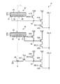
- FIG. 3 is a circuit diagram showing a circuit configuration of a unit pixel according to an embodiment of the present disclosure.
- FIG. 6 is a cross-sectional view schematically showing the structure of a pixel array section according to another embodiment of the present disclosure.
- FIG. 6 is a cross-sectional view schematically showing the structure of a pixel array section according to another embodiment of the present disclosure.
- FIG. 6 is a cross-sectional view schematically showing the structure of a pixel array section according to another embodiment of the present disclosure.
- FIG. 11 is a cross-sectional view schematically showing the structure of a pixel array section according to Modification Example 1 of the embodiment of the present disclosure.
- FIG. 11 is a cross-sectional view schematically showing the structure of a pixel array section according to Modification 2 of the embodiment of the present disclosure.
- FIG. 11 is a cross-sectional view schematically showing the structure of a pixel array section according to Modification 3 of the embodiment of the present disclosure.
- FIG. 11 is a cross-sectional view schematically showing the structure of a pixel array section according to Modification 4 of the embodiment of the present disclosure.
- FIG. 11 is a circuit diagram showing a circuit configuration of a unit pixel according to Modification 4 of the embodiment of the present disclosure.
- FIG. 11 is a circuit diagram showing a circuit configuration of a unit pixel according to Modification 4 of the embodiment of the present disclosure.
- FIG. 11 is a cross-sectional view schematically showing the structure of a pixel array section according to Modification 5 of the embodiment of the present disclosure.
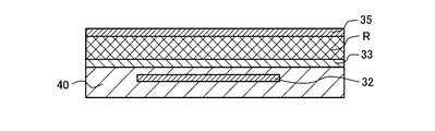
- FIG. 6 is a cross-sectional view schematically showing one manufacturing process of the pixel array section according to the embodiment of the present disclosure.
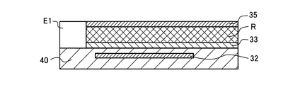
- FIG. 6 is a cross-sectional view schematically showing one manufacturing process of the pixel array section according to the embodiment of the present disclosure.
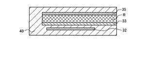
- FIG. 6 is a cross-sectional view schematically showing one manufacturing process of the pixel array section according to the embodiment of the present disclosure.
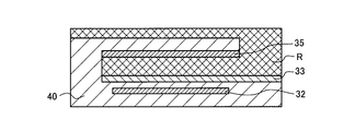
- FIG. 6 is a cross-sectional view schematically showing one manufacturing process of the pixel array section according to the embodiment of the present disclosure.
- FIG. 6 is a cross-sectional view schematically showing one manufacturing process of the pixel array section according to the embodiment of the present disclosure.
- FIG. 6 is a cross-sectional view schematically showing one manufacturing process of the pixel array section according to the embodiment of the present disclosure.
- FIG. 6 is a cross-sectional view schematically showing one manufacturing process of the pixel array section according to the embodiment of the present disclosure.
- FIG. 6 is a cross-sectional view schematically showing one manufacturing process of the pixel array section according to the embodiment of the present disclosure.
- FIG. 6 is a cross-sectional view schematically showing one manufacturing process of the pixel array section according to the embodiment of the present disclosure.
- FIG. 6 is a cross-sectional view schematically showing one manufacturing process of the pixel array section according to the embodiment of the present disclosure.
- FIG. 6 is a cross-sectional view schematically showing one manufacturing process of the pixel array section according to the embodiment of the present disclosure.
- FIG. 6 is a cross-sectional view schematically showing one manufacturing process of the pixel array section according to the embodiment of the present disclosure.
- FIG. 6 is a cross-sectional view schematically showing one manufacturing process of the pixel array section according to the embodiment of the present disclosure.
- FIG. 6 is a cross-sectional view schematically showing one manufacturing process of the pixel array section according to the embodiment of the present disclosure.
- FIG. 6 is a cross-sectional view schematically showing one manufacturing process of the pixel array section according to the embodiment of the present disclosure.
- FIG. 6 is a cross-sectional view schematically showing one manufacturing process of the pixel array section according to the embodiment of the present disclosure.
- FIG. 6 is a cross-sectional view schematically showing one manufacturing process of the pixel array section according to the embodiment of the present disclosure.
- FIG. 6 is a cross-sectional view schematically showing one manufacturing process of the pixel array section according to the embodiment of the present disclosure.
- FIG. 6 is a cross-sectional view schematically showing one manufacturing process of the pixel array section according to the embodiment of the present disclosure.
- FIG. 6 is a cross-sectional view schematically showing one manufacturing process of the pixel array section according to the embodiment of the present disclosure.
- FIG. 6 is a cross-sectional view schematically showing one manufacturing process of the pixel array section according to the embodiment of the present disclosure. It is sectional drawing which shows typically one manufacturing process of the pixel array part which concerns on embodiment of this disclosure.
- FIG. 11 is a cross-sectional view schematically showing one manufacturing process of the pixel array section according to Modification Example 1 of the embodiment of the present disclosure.
- FIG. 11 is a cross-sectional view schematically showing one manufacturing process of the pixel array section according to Modification Example 1 of the embodiment of the present disclosure.
- FIG. 11 is a cross-sectional view schematically showing one manufacturing process of the pixel array section according to Modification Example 1 of the embodiment of the present disclosure.
- FIG. 11 is a cross-sectional view schematically showing one manufacturing process of the pixel array section according to Modification Example 1 of the embodiment of the present disclosure.
- FIG. 11 is a cross-sectional view schematically showing one manufacturing process of the pixel array section according to Modification Example 1 of the embodiment of the present disclosure.
- FIG. 11 is a cross-sectional view schematically showing one manufacturing process of the pixel array section according to Modification 2 of the embodiment of the present disclosure.
- FIG. 11 is a cross-sectional view schematically showing one manufacturing process of the pixel array section according to Modification 2 of the embodiment of the present disclosure.
- FIG. 11 is a cross-sectional view schematically showing one manufacturing process of the pixel array section according to Modification 2 of the embodiment of the present disclosure.
- FIG. 11 is a cross-sectional view schematically showing one manufacturing process of the pixel array section according to Modification 2 of the embodiment of the present disclosure.
- FIG. 11 is a cross-sectional view schematically showing one manufacturing process of the pixel array section according to Modification 2 of the embodiment of the present disclosure.
- FIG. 11 is a cross-sectional view schematically showing one manufacturing process of the pixel array section according to Modification 2 of the embodiment of the present disclosure.
- FIG. 14 is a cross-sectional view schematically showing one manufacturing process of the pixel array section according to Modification 3 of the embodiment of the present disclosure.
- FIG. 14 is a cross-sectional view schematically showing one manufacturing process of the pixel array section according to Modification 3 of the embodiment of the present disclosure.
- FIG. 14 is a cross-sectional view schematically showing one manufacturing process of the pixel array section according to Modification 3 of the embodiment of the present disclosure.
- FIG. 14 is a cross-sectional view schematically showing one manufacturing process of the pixel array section according to Modification 3 of the embodiment of the present disclosure.
- FIG. 14 is a cross-sectional view schematically showing one manufacturing process of the pixel array section according to Modification 3 of the embodiment of the present disclosure.
- FIG. 14 is a cross-sectional view schematically showing one manufacturing process of the pixel array section according to Modification 3 of the embodiment of the present disclosure.
- FIG. 14 is a cross-sectional view schematically showing one manufacturing process of the pixel array section according to Modification 3 of the embodiment of the present disclosure.
- FIG. 14 is a cross-sectional view schematically showing one manufacturing process of the pixel array section according to Mod
- FIG. 14 is a cross-sectional view schematically showing one manufacturing process of the pixel array section according to Modification 3 of the embodiment of the present disclosure.
- FIG. 14 is a cross-sectional view schematically showing one manufacturing process of the pixel array section according to Modification 3 of the embodiment of the present disclosure.
- FIG. 14 is a cross-sectional view schematically showing one manufacturing process of the pixel array section according to Modification 3 of the embodiment of the present disclosure. It is sectional drawing which shows typically one manufacturing process of the pixel array part which concerns on another example of modification 3 of embodiment of this disclosure.
- FIG. 14 is a cross-sectional view schematically showing one manufacturing process of the pixel array section according to another example of Modification Example 3 of the embodiment of the present disclosure.
- FIG. 14 is a cross-sectional view schematically showing one manufacturing process of the pixel array section according to another example of Modification Example 3 of the embodiment of the present disclosure. It is sectional drawing which shows typically one manufacturing process of the pixel array part which concerns on another example of modification 3 of embodiment of this disclosure.
- FIG. 14 is a cross-sectional view schematically showing one manufacturing process of the pixel array section according to another example of Modification Example 3 of the embodiment of the present disclosure. It is sectional drawing which shows typically one manufacturing process of the pixel array part which concerns on another example of modification 3 of embodiment of this disclosure.
- FIG. 16 is a cross-sectional view schematically showing one manufacturing process of the pixel array section according to Modification 4 of the embodiment of the present disclosure.
- FIG. 16 is a cross-sectional view schematically showing one manufacturing process of the pixel array section according to Modification 4 of the embodiment of the present disclosure.
- FIG. 16 is a cross-sectional view schematically showing one manufacturing process of the pixel array section according to Modification 4 of the embodiment of the present disclosure.
- FIG. 16 is a cross-sectional view schematically showing one manufacturing process of the pixel array section according to Modification 4 of the embodiment of the present disclosure.
- FIG. 16 is a cross-sectional view schematically showing one manufacturing process of the pixel array section according to Modification 4 of the embodiment of the present disclosure.
- FIG. 16 is a cross-sectional view schematically showing one manufacturing process of the pixel array section according to Modification 4 of the embodiment of the present disclosure.
- FIG. 16 is a cross-sectional view schematically showing one manufacturing process of the pixel array section according to Modification 4 of the embodiment of the present disclosure.
- FIG. 16 is a cross-sectional view schematically showing one manufacturing process of the pixel array section according to Modification 4 of the embodiment of the present disclosure.
- FIG. 16 is a cross-sectional view schematically showing one manufacturing process of the pixel array section according to Modification 4 of the embodiment of the present disclosure.
- FIG. 16 is a cross-sectional view schematically showing one manufacturing process of the pixel array section according to Modification 4 of the embodiment of the present disclosure.
- FIG. 16 is a cross-sectional view schematically showing one manufacturing process of the pixel array section according to Modification 4 of the embodiment of the present disclosure.
- FIG. 16 is a cross-sectional view schematically showing one manufacturing process of the pixel array section according to Modification 4 of the embodiment of the present disclosure.
- FIG. 16 is a cross-sectional view schematically showing one manufacturing process of the pixel array section according to Modification 4 of the embodiment of the present disclosure.
- FIG. 16 is a cross-sectional view schematically showing one manufacturing process of the pixel array section according to Modification 4 of the embodiment of the present disclosure. It is a top view which shows typically an example of arrangement
- FIG. 20 is a block diagram illustrating a configuration example of an imaging device as an electronic device to which the technology according to the present disclosure is applied.
- the annealing process may damage the photoelectric conversion layer that is an organic material.
- the annealing temperature is set lower than the heat-resistant temperature of the photoelectric conversion layer so that the photoelectric conversion layer is not damaged, the desired annealing effect cannot be obtained, and thus it is difficult to obtain good device characteristics.
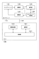
- FIG. 1 is a system configuration diagram illustrating a schematic configuration example of a solid-state imaging device 1 according to an embodiment of the present disclosure.
- the solid-state imaging device 1 which is a CMOS image sensor includes a pixel array unit 10, a system control unit 12, a vertical drive unit 13, a column read circuit unit 14, a column signal processing unit 15, and A horizontal drive unit 16 and a signal processing unit 17 are provided.
- the pixel array unit 10, the system control unit 12, the vertical drive unit 13, the column read circuit unit 14, the column signal processing unit 15, the horizontal drive unit 16, and the signal processing unit 17 are electrically connected to each other on the same semiconductor substrate. It is provided on a plurality of laminated semiconductor substrates.
- the pixel array unit 10 has a photoelectric conversion element (such as the photoelectric conversion unit 30 (see FIG. 2)) capable of photoelectrically converting the amount of charge according to the amount of incident light, accumulating it internally, and outputting it as a signal.
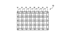
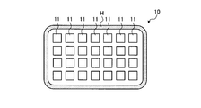
- Unit pixels (hereinafter, also referred to as “unit pixels”) 11 are two-dimensionally arranged in a matrix.
- the pixel array unit 10 includes, in addition to the effective unit pixel 11, a dummy unit pixel having a structure that does not have a photoelectric conversion unit 30 or the like, or a light-shielding unit pixel in which light from the outside is blocked by shielding the light-receiving surface. May include areas arranged in rows and/or columns.
- the light-shielding unit pixel may have the same configuration as the effective unit pixel 11 except that the light-receiving surface is shielded from light. Further, in the following, the photocharge having the charge amount corresponding to the incident light amount may be simply referred to as “charge”, and the unit pixel 11 may be simply referred to as “pixel”.
- a pixel drive line LD is formed for each row along a left-right direction (arrangement direction of pixels in a pixel row) in the drawing with respect to a matrix of pixel arrays, and a vertical pixel wiring is provided for each column.
- the LVs are formed along the vertical direction (arrangement direction of pixels in the pixel column) in the drawing.
- One end of the pixel drive line LD is connected to the output end corresponding to each row of the vertical drive unit 13.
- the column read circuit unit 14 includes at least a circuit that supplies a constant current to the unit pixels 11 in a selected row in the pixel array unit 10 for each column, a current mirror circuit, and a changeover switch of the unit pixel 11 to be read.
- the column readout circuit unit 14 forms an amplifier together with the transistor in the selected pixel in the pixel array unit 10, converts the photocharge signal into a voltage signal and outputs it to the vertical pixel wiring LV.
- the vertical drive unit 13 includes a shift register, an address decoder, and the like, and drives each unit pixel 11 of the pixel array unit 10 at the same time for all pixels or in line units.
- the vertical drive unit 13 has a read scanning system and a sweep scanning system or a batch sweep and batch transfer system, although the specific construction thereof is not shown.
- the read-out scanning system selectively scans the unit pixels 11 of the pixel array unit 10 row by row in order to read the pixel signal from the unit pixels 11.
- a sweeping scan is performed prior to the read scan by a shutter speed time with respect to the read row in which the read scan system performs the read scan.
- batch sweeping is performed prior to batch transfer by the time of shutter speed.
- unnecessary charges are swept (reset) from the photoelectric conversion unit 30 and the like of the unit pixel 11 of the read line.
- the so-called electronic shutter operation is performed by sweeping out (resetting) the unnecessary charges.
- the electronic shutter operation is an operation of discarding unnecessary photocharges accumulated in the photoelectric conversion unit 30 and the like until immediately before and newly starting exposure (starting accumulation of photocharges).
- the signal read by the read operation by the read scanning system corresponds to the amount of light incidented after the read operation immediately before or the electronic shutter operation.
- the period from the read timing of the immediately previous read operation or the sweep timing of the electronic shutter operation to the read timing of the current read operation is the photocharge accumulation time (exposure time) in the unit pixel 11.
- the time from batch sweep to batch transfer is the accumulation time (exposure time).
- the pixel signal output from each unit pixel 11 in the pixel row selectively scanned by the vertical drive unit 13 is supplied to the column signal processing unit 15 through each vertical pixel wiring LV.
- the column signal processing unit 15 performs, for each pixel column of the pixel array unit 10, predetermined signal processing on a pixel signal output from each unit pixel 11 in a selected row through the vertical pixel wiring LV, and after the signal processing, Temporarily holds the pixel signal.
- the column signal processing unit 15 performs at least noise removal processing, such as CDS (Correlated Double Sampling) processing, as signal processing.
- CDS Correlated Double Sampling
- the column signal processing unit 15 performs at least noise removal processing, such as CDS (Correlated Double Sampling) processing, as signal processing.
- CDS Correlated Double Sampling
- fixed pattern noise peculiar to the pixel such as reset noise and threshold variation of the amplification transistor AMP is removed.
- the column signal processing unit 15 can be configured to have, for example, an AD conversion function in addition to the noise removal processing, and output the pixel signal as a digital signal.
- the horizontal drive unit 16 includes a shift register, an address decoder, and the like, and sequentially selects a unit circuit corresponding to the pixel sequence of the column signal processing unit 15. By the selective scanning by the horizontal drive unit 16, the pixel signals signal-processed by the column signal processing unit 15 are sequentially output to the signal processing unit 17.
- the system control unit 12 includes a timing generator that generates various timing signals, and based on the various timing signals generated by the timing generator, the vertical drive unit 13, the column signal processing unit 15, the horizontal drive unit 16, and the like. Drive control is performed.
- the solid-state imaging device 1 further includes a signal processing unit 17 and a data storage unit (not shown).
- the signal processing unit 17 has at least an addition processing function, and performs various signal processing such as addition processing on the pixel signal output from the column signal processing unit 15.
- the data storage unit temporarily stores the data necessary for the signal processing in the signal processing unit 17 during the signal processing.
- the signal processing unit 17 and the data storage unit may be an external signal processing unit provided on a board different from the solid-state imaging device 1, for example, a DSP (Digital Signal Processor) or software processing. It may be mounted on the same substrate as 1.
- DSP Digital Signal Processor
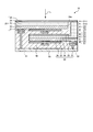
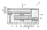
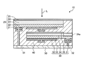
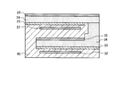
- FIG. 2 is a cross-sectional view schematically showing the structure of the pixel array section 10 according to the embodiment of the present disclosure
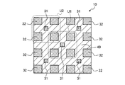
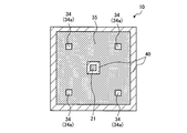
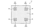
- FIGS. 3A to 3K are plan structural views of the depths D1 to D11 shown in FIG.
- the pixel array unit 10 includes a photoelectric conversion unit 20, a photoelectric conversion unit 30, an insulating layer 40, and a semiconductor layer 50.
- the photoelectric conversion unit 30 is provided on the light incident side of the semiconductor layer 50 (the side on which the light L is incident from the outside), and the photoelectric conversion unit 20 is provided on the light incident side of the photoelectric conversion unit 30.
- the photoelectric conversion unit 20 and the photoelectric conversion unit 30 are provided one by one for each unit pixel 11 (see FIG. 1). That is, a plurality of photoelectric conversion units 20 and a plurality of photoelectric conversion units 30 are provided in the entire pixel array unit 10.
- the photoelectric conversion unit 20 has a first electrode 21, a charge storage electrode 22, a charge storage layer 23, a photoelectric conversion layer 24, and a second electrode 25.
- the first electrode 21 is provided on the side opposite to the light incident side in the photoelectric conversion unit 20.
- the first electrode 21 has a surface on the light incident side (hereinafter, also referred to as “top surface”) opposite to the light incident side of the charge storage layer 23 (hereinafter, also referred to as “bottom surface”). ).
- the first electrode 21 extends in the insulating layer 40 in the depth direction and is connected to the floating diffusion 51 provided in the semiconductor layer 50. That is, the first electrode 21 electrically connects the charge storage layer 23 and the floating diffusion 51.
- the first electrode 21 is composed of a light-transmitting conductor, that is, a so-called transparent conductor.
- the first electrode 21 is made of, for example, ITO (Indium Tin Oxide).
- the constituent material of the first electrode 21 is not limited to ITO, and may be a tin oxide (SnO 2 ) based material, a zinc oxide (ZnO) based material, or the like.
- Examples of such a zinc oxide-based material include AZO (Aluminum Zinc Oxide), GZO (Gallium Zinc Oxide), and IZO (Indium Zinc Oxide).
- AZO Alignium Zinc Oxide
- IZO Indium Zinc Oxide
- CuI, InSbO 4 , ZnMgO, CuInO 2 , MgIn 2 O 4 , CdO, ZnSnO 3 or the like may be used.
- the charge storage electrode 22 is composed of a transparent conductor such as ITO, AZO, GZO, and IZO.
- the constituent material of the charge storage electrode 22 is not limited to these transparent conductors, and may be the same material as the various transparent conductors exemplified in the description of the first electrode 21.
- the charge storage electrode 22 is provided adjacent to the first electrode 21 via the insulating layer 40.
- the unit U1 shown in FIG. 3G is one unit in which the plurality of (four in FIG. 3G) photoelectric conversion units 20 share the floating diffusion 51.
- the charge storage layer 23 is made of a semiconductor material having a large band gap, high carrier mobility, and light transmission.
- the charge storage layer 23 has, for example, a band gap of 3.0 (eV) or more, a higher carrier mobility than the material forming the photoelectric conversion layer 24, and an impurity concentration of 1 ⁇ 10 18 (cm ⁇ 3 ) or less. Are preferred.
- the charge storage layer 23 is composed of, for example, an oxide semiconductor, an organic semiconductor, a two-dimensional semiconductor, or the like.
- an oxide semiconductor for example, a chalcogenite-based oxide semiconductor or IGZO (Indium Gallium Zinc Oxide) can be used.
- organic semiconductor for example, rubrene, tetracene, pentacene, peryleneimide, tetracyanoquinodimethane and the like, which are low molecular weight organic materials having an aromatic ring such as a condensed polycyclic hydrocarbon compound and a condensed heterocyclic compound, can be used. it can.
- organic semiconductor polythiophene, polyacetylene, polyparaphenylene vinylene, etc., which are ⁇ -electron conjugated conductive polymers, may be used.
- organic semiconductor silicon carbide, diamond, graphene, carbon nanotubes, condensed polycyclic hydrocarbon compounds, condensed heterocyclic compounds and the like may be used.
- the two-dimensional semiconductor includes, for example, molybdenum disulfide (MoS 2 ), tungsten disulfide (WS 2 ), hafnium disulfide (HfS 2 ), hexagonal boron nitride (hBN), indium selenium (InSe), and transition.
- MoS 2 molybdenum disulfide
- WS 2 tungsten disulfide
- HfS 2 hafnium disulfide
- hBN hexagonal boron nitride
- InSe indium selenium
- transition a metal dicalcogenide or the like can be used.
- the charge accumulation layer 23 is preferably a material having an ionization potential larger than that of the material forming the photoelectric conversion layer 24.
- the charge storage layer 23 is preferably a material having an electron affinity smaller than that of the material forming the photoelectric conversion layer 24.
- the charge storage tank 23 may have a single-layer structure or a multi-layer structure. Further, the material constituting the charge storage layer 23 located above the charge storage electrode 22 and the material constituting the charge storage layer 23 located above the first electrode 21 may be different.
- the upper surface of the charge storage layer 23 is in contact with the bottom surface of the photoelectric conversion layer 24, and the bottom surface of the charge storage layer 23 is in contact with the upper surface of the first electrode 21.
- the bottom surface of the charge storage layer 23 is adjacent to the charge storage electrode 22 with the insulating layer 40 interposed therebetween. Then, when a predetermined voltage is applied to the charge storage electrode 22, the charge photoelectrically converted by the photoelectric conversion layer 24 is accumulated in the charge storage layer 23.
- the photoelectric conversion layer 24 is provided so as to cover the upper surface of the charge storage layer 23.
- the photoelectric conversion layer 24 is made of an organic semiconductor material, and performs photoelectric conversion of light having a wavelength (for example, blue) selected from the light L incident from the outside.
- the photoelectric conversion layer 24 contains one or both of a p-type organic semiconductor and an n-type organic semiconductor.
- the photoelectric conversion layer 24 is composed of, for example, quinacridone, a quinacridone derivative, a subphthalocyanine and a subphthalocyanine derivative, and it is desirable that the photoelectric conversion layer 24 contains at least one of these materials.
- the photoelectric conversion layer 24 is not limited to such a material, and may be, for example, at least one of naphthalene, anthracene, phenanthrene, tetracene, pyrene, perylene, fluoranthene, and the like (all of which include derivatives).
- the photoelectric conversion layer 24 may use a polymer or derivative such as phenylene vinylene, fluorene, carbazole, indole, pyrene, pyrrole, picoline, thiophene, acetylene and diacetylene.
- a metal complex dye a cyanine dye, a merocyanine dye, a phenylxanthene dye, a triphenylmethane dye, a rodacyanine dye, a xanthene dye, or the like may be used.
- the photoelectric conversion layer 24 may contain other organic materials such as fullerene (C 60 ) and BCP (Bathocuproine) in addition to the organic semiconductor dye.
- a coumarin acid dye for example, tris-8-hydroxyquinolialuminum (Alq3), a melanin dye, or the like can be used for the photoelectric conversion layer 24.
- the second electrode 25 is provided so as to be in contact with the upper surface of the photoelectric conversion layer 24 and cover the upper surface.
- the second electrode 25 is composed of a transparent conductor such as ITO, AZO, GZO, and IZO.
- the constituent material of the second electrode 25 is not limited to these transparent conductors, and may be the same material as the various transparent conductors illustrated when the first electrode 21 is described.
- the photoelectric conversion unit 30 is provided on the bottom surface side of the photoelectric conversion unit 20 so as to be laminated on the photoelectric conversion unit 20.
- the photoelectric conversion unit 30 includes a first electrode 31, a charge storage electrode 32, a charge storage layer 33, a photoelectric conversion layer 34, and a second electrode 35.
- the first electrode 31 is provided on the photoelectric conversion unit 30 on the side opposite to the light incident side. In addition, the first electrode 31 contacts the bottom surface of the charge storage layer 33 at the top surface.
- the first electrode 31 extends in the insulating layer 40 in the depth direction and is connected to the floating diffusion 52 provided in the semiconductor layer 50. That is, the first electrode 31 electrically connects the charge storage layer 33 and the floating diffusion 52.
- the first electrode 31 is composed of a transparent conductor such as ITO, AZO, GZO, and IZO.
- the constituent material of the first electrode 31 is not limited to these transparent conductors, and may be the same as the various transparent conductors exemplified when the first electrode 21 is described.
- the charge storage electrode 32 is composed of a transparent conductor such as ITO, AZO, GZO, and IZO. Note that the constituent material of the charge storage electrode 32 is not limited to these transparent conductors, and may be the same as the various transparent conductors exemplified when the first electrode 21 is described.
- the charge storage electrode 32 is provided adjacent to the first electrode 31 with the insulating layer 40 interposed therebetween.
- the unit U2 shown in FIG. 3A is one unit in which the floating diffusions 52 are shared by a plurality (four in FIG. 3A) of photoelectric conversion units 30.
- the charge storage layer 33 is made of a semiconductor material having a large band gap, high carrier mobility, and light transmittance.
- the constituent material of the charge storage tank 33 the same materials as the various semiconductor materials exemplified when the charge storage layer 23 is described can be used.
- the top surface of the charge storage layer 33 contacts the bottom surface of the photoelectric conversion layer 34, and the bottom surface of the charge storage layer 33 contacts the top surface of the first electrode 31. Further, the bottom surface of the charge storage layer 33 is adjacent to the charge storage electrode 32 via the insulating layer 40.
- a predetermined voltage is applied to the charge storage electrode 32, the charges photoelectrically converted by the photoelectric conversion layer 34 are stored in the charge storage layer 33.
- the photoelectric conversion layer 34 is provided so as to cover the upper surface of the charge storage layer 33.
- the photoelectric conversion layer 34 is made of an organic semiconductor material, and photoelectrically converts light having a selective wavelength (for example, green) of the light L incident from the outside.
- the photoelectric conversion layer 34 preferably includes one or both of a p-type organic semiconductor and an n-type organic semiconductor.
- a p-type organic semiconductor and an n-type organic semiconductor the same materials as the various materials exemplified in the description of the photoelectric conversion layer 24 can be used.
- a rhodamine-based dye for example, a rhodamine-based dye, a melancyanine-based dye, a quinacridone derivative, a subphthalocyanine-based dye (subphthalocyanine derivative) or the like can be used for the photoelectric conversion layer 34.
- the second electrode 35 is provided so as to be in contact with the upper surface of the photoelectric conversion layer 34.
- the second electrode 35 is composed of a transparent conductor such as ITO, AZO, GZO, IZO.
- the constituent material of the second electrode 35 is not limited to these transparent conductors, and may be the same material as the various transparent conductors exemplified when the first electrode 21 is described.
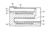
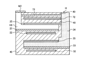
- the photoelectric conversion layer 34 of the photoelectric conversion unit 30 is second in plan view (that is, when viewed from the side on which the light L is incident). It has a protruding region 34 a that protrudes from the electrode 35.
- a surface on the light incident side of the protruding region 34a is closer to the light incident side than a portion of the photoelectric conversion layer 34 in contact with the second electrode 35 (that is, a portion other than the protruding region 34a of the photoelectric conversion layer 34). It is provided so as to project.
- the portion corresponding to the protruding region 34a can be used as an injection port through which a liquid solvent (for example, an organic solvent) can be injected in the coating process. That is, after forming a portion of the pixel array unit 10 other than the photoelectric conversion layer 34, the liquid raw material can be injected into the portion corresponding to the photoelectric conversion layer 34 through the injection port.
- a liquid solvent for example, an organic solvent
- the liquid raw material can be produced by dissolving the raw material of the photoelectric conversion layer 34 in an organic solvent or the like.
- the photoelectric conversion layer 34 can be formed by drying the liquid raw material injected into the portion corresponding to the photoelectric conversion layer 34 at a predetermined temperature.
- the photoelectric conversion layer 34 can be formed after the semiconductor process to some extent is completed by using the portion corresponding to the protruding region 34a as the injection port for injecting the liquid raw material. Detailed manufacturing steps of the pixel array section 10 according to this embodiment will be described later.
- the insulating layer 40 is provided on the upper surface of the semiconductor layer 50, and is provided so as to surround the photoelectric conversion unit 20 and the photoelectric conversion unit 30.
- the insulating layer 40 is made of a light-transmitting insulator.
- the insulating layer 40 is made of, for example, silicon oxide (SiO 2 ), silicon nitride (SiN), aluminum oxide (Al 2 O 3 ), or the like.
- the semiconductor layer 50 includes, for example, silicon.
- the semiconductor layer 50 has a photodiode 60 (see FIG. 4) at a position overlapping the photoelectric conversion unit 20 and the photoelectric conversion unit 30 in a plan view.
- the photodiode 60 photoelectrically converts light having a wavelength different from that of the light L incident from the outside by the photoelectric conversion unit 20 and the photoelectric conversion unit 30 (for example, red).
- one unit pixel 11 is provided with a photoelectric conversion unit 20, a photoelectric conversion unit 30, and a photodiode 60, and the photoelectric conversion unit 20, the photoelectric conversion unit 30, and the photodiode 60 provide three colors of light. Are photoelectrically converted.
- the color information of three colors can be obtained by one unit pixel 11 without using a color filter. Can get all.
- the embodiment it is possible to suppress attenuation of the light L incident on the color filter, and thus it is possible to obtain a high-quality image.
- the photoelectric conversion section 20 including the photoelectric conversion layer 24 made of an organic semiconductor material and the photoelectric conversion section 30 including the photoelectric conversion layer 34 also made of the organic semiconductor material It is provided by stacking.
- the photoelectric conversion unit 20 and the photoelectric conversion unit 30 can suppress the attenuation of the light L, so that a higher quality image can be acquired.
- the semiconductor layer 50 is provided with a floating diffusion 51 corresponding to the photoelectric conversion unit 20 and a floating diffusion 52 corresponding to the photoelectric conversion unit 30.
- the semiconductor layer 50 is provided with a plurality of pixel transistors that read out the charges accumulated in the photoelectric conversion units 20 and 30 and the photodiode 60, and a multilayer wiring layer including a plurality of wiring layers and an interlayer insulating film.
- a multilayer wiring layer including a plurality of wiring layers and an interlayer insulating film.
- an on-chip lens or the like that collects light L is provided on the light incident side of the photoelectric conversion unit 20, but the on-chip lens or the like is not shown.
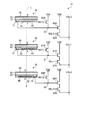
- FIG. 4 is a circuit diagram showing an example of a circuit configuration of the unit pixel 11 according to the embodiment of the present disclosure.
- the unit pixel 11 has a floating diffusion 51, a reset transistor 61R, an amplification transistor 61A, and a selection transistor 61S as a circuit for reading out electric charges from the photoelectric conversion unit 20.
- a predetermined voltage is applied to the first electrode 21, the charge storage electrode 22, and the second electrode 25 from a drive circuit (not shown) during the charge storage period. For example, during the charge storage period, a positive voltage is applied to the first electrode 21 and the charge storage electrode 22, and a negative voltage is applied to the second electrode 25. Further, in the charge storage period, a larger positive voltage is applied to the charge storage electrode 22 than the first electrode 21.
- the electrons included in the charges photoelectrically converted in the photoelectric conversion layer 24 are attracted by the large positive voltage of the charge storage electrode 22 and are stored in the charge storage layer 23. ..
- the reset operation is performed by operating the reset transistor 61R in the latter half of the charge accumulation period.
- the potential of the floating diffusion 51 is reset, and the potential of the floating diffusion 51 becomes the power supply voltage Vdd.
- the charge transfer operation is performed after the completion of the reset operation.
- a positive voltage higher than that of the charge storage electrode 22 is applied to the first electrode 21 from the drive circuit.
- the electrons accumulated in the charge storage layer 23 are transferred to the floating diffusion 51 via the first electrode 21.
- a series of operations such as a charge storage operation, a reset operation, and a charge transfer operation are completed by the above operations.
- the floating diffusion 51 holds the charges read from the photoelectric conversion unit 20.
- the reset transistor 61R is turned on by the reset signal RST1
- the charge accumulated in the floating diffusion 51 is discharged to the drain (power supply voltage Vdd) to reset the potential of the floating diffusion 51.
- the amplification transistor 61A outputs a pixel signal indicating a level corresponding to the charge accumulated in the floating diffusion 51 to the signal line VSL1 via the selection transistor 61S.
- the selection transistor 61S is turned on when the unit pixel 11 is selected by the selection signal SEL1, and outputs the pixel signal generated by the photoelectric conversion unit 20 to the vertical signal line VSL1.
- the unit pixel 11 has a floating diffusion 52, a reset transistor 62R, an amplification transistor 62A, and a selection transistor 62S as a circuit for performing reading of charges from the photoelectric conversion unit 30.
- the unit pixel 11 has a transfer transistor 63T, a floating diffusion 53, a reset transistor 63R, an amplification transistor 63A, and a selection transistor 63S as a circuit for reading out electric charges from the photodiode 60.
- the photodiode 60 generates and accumulates electric charge according to the amount of received light.
- the anode terminal of the photodiode 60 is grounded, and the cathode terminal is connected to the floating diffusion 53 via the transfer transistor 63T.
- the transfer transistor 63T When the transfer transistor 63T is turned on by the transfer signal TG3, it reads out the electric charge generated by the photodiode 60 and transfers it to the floating diffusion 53.
- the floating diffusion 53 holds the charges read from the photodiode 60.
- the reset transistor 63R is turned on by the reset signal RST3
- the electric charge accumulated in the floating diffusion 53 is discharged to the drain (power supply voltage Vdd) to reset the potential of the floating diffusion 53.
- the amplification transistor 63A outputs a pixel signal indicating a level corresponding to the electric charge accumulated in the floating diffusion 53 to the signal line VSL3 via the selection transistor 63S.
- the selection transistor 63S is turned on when the unit pixel 11 is selected by the selection signal SEL3, and outputs the pixel signal generated by the photodiode 60 to the vertical signal line VSL3.
- the pixel array unit 10 by providing the charge storage electrode 22 and the charge storage layer 23 in the photoelectric conversion unit 20, it is possible to reduce the reset noise during the reset operation by the reset transistor 61R. Therefore, according to the embodiment, a high quality image can be acquired.
- the pixel array unit 10 by providing the charge storage electrode 32 and the charge storage layer 33 in the photoelectric conversion unit 30, it is possible to reduce the reset noise during the reset operation by the reset transistor 62R. Therefore, according to the embodiment, a high quality image can be acquired.
- a plurality of photoelectric conversion units 20 included in the unit U1 share the floating diffusion 51. This eliminates the need to provide the individual floating diffusions 51 for all the photoelectric conversion units 20, so that the circuit configuration in the pixel array unit 10 can be simplified.
- the manufacturing cost of the pixel array unit 10 can be reduced.
- the plurality of photoelectric conversion units 30 included in the unit U2 share the floating diffusion 52. This eliminates the need to provide individual floating diffusion 52s in all the photoelectric conversion units 30, so that the circuit configuration in the pixel array unit 10 can be simplified.
- the manufacturing cost of the pixel array unit 10 can be reduced.
- a plurality of photodiodes 60 may share the floating diffusion 53. Accordingly, it is not necessary to provide the individual floating diffusions 53 for all the photodiodes 60, so that the circuit configuration in the pixel array section 10 can be simplified.
- the manufacturing cost of the pixel array unit 10 can be reduced.
- the circuit in the unit pixel 11 can be configured as described above, but is not limited to this configuration, and another configuration can be adopted.
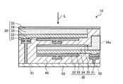
- FIG. 5 is a cross-sectional view schematically showing the structure of the pixel array unit 10 according to another embodiment of the present disclosure.
- the global shutter function can be imparted to the photoelectric conversion unit 30 of the pixel array unit 10 by simultaneously transferring the charge charged by photoelectric conversion to the charge holding region 54.
- FIG. 6 is a sectional view schematically showing the structure of the pixel array section 10 according to another embodiment of the present disclosure.
- the global shutter function can be imparted to the photoelectric conversion unit 30 of the pixel array unit 10 by simultaneously transferring the charge charged by photoelectric conversion to the charge holding region 33a for all the pixels.
- the protruding region 34a can be used as a substantial light shielding layer.
- the protruding region 34 a when the protruding region 34 a is provided so as to project to the light incident side from the portion of the photoelectric conversion layer 34 in contact with the second electrode 35 and reach the second electrode 25,
- the protruding region 34a has a high light shielding performance. Therefore, by providing the protruding region 34a so as to project to the light incident side, a highly accurate global shutter function can be provided.
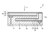
- FIG. 7 is a cross-sectional view schematically showing the structure of the pixel array section 10 according to another embodiment of the present disclosure.
- the photoelectric conversion unit 20 is composed of the first electrode 21, the photoelectric conversion layer 24, and the second electrode 25, and the photoelectric conversion unit 30 is the first electrode 31, the photoelectric conversion layer 34, and the second electrode 35. Composed of.
- the electrons contained in the electric charge generated by the photoelectric conversion in the photoelectric conversion layer 24 (or the photoelectric conversion layer 34) move to the first electrode 21 (or the first electrode 31). Then, the electrons that have moved to the first electrode 21 (or the first electrode 31) are transferred to the floating diffusion 51 (or the floating diffusion 52).
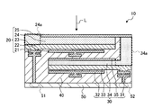
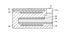
- FIG. 8 is a cross-sectional view schematically showing the structure of the pixel array unit 10 according to the first modification of the embodiment of the present disclosure.
- the configuration of the protruding region 34a in the photoelectric conversion layer 34 is different from that of the embodiment. Specifically, in the protruding region 34a of Modification 1, the surface on the light incident side of the photoelectric conversion layer 34 in contact with the second electrode 35 is provided so as to project to the light incident side, while the second electrode 25 is provided. Has not reached.
- the portion corresponding to the protruding region 34a can be used as an injection port through which the liquid raw material can be injected, as in the embodiment. That is, after forming a portion of the pixel array unit 10 other than the photoelectric conversion layer 34, the liquid raw material can be injected into the portion corresponding to the photoelectric conversion layer 34 through the injection port.
- the photoelectric conversion layer 34 can be formed by drying the liquid raw material injected into the portion corresponding to the photoelectric conversion layer 34 at a predetermined temperature. Therefore, according to the first modification, the photoelectric conversion layer 34 can be formed after a certain degree of semiconductor process is completed. Detailed manufacturing steps of the pixel array section 10 according to the first modification will be described later.
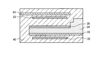
- FIG. 9 is a cross-sectional view schematically showing the structure of the pixel array section 10 according to Modification 2 of the embodiment of the present disclosure.
- the configuration of the protruding region 34a in the photoelectric conversion layer 34 is different from that of the embodiment and Modification 1. Specifically, in the protruding area 34a of Modification 2, the surface of the photoelectric conversion layer 34 in contact with the second electrode 35 and the surface on the light incident side are substantially flush with each other.
- the portion corresponding to the protruding region 34a can be used as an injection port into which the liquid raw material can be injected. That is, after forming a portion of the pixel array unit 10 other than the photoelectric conversion layer 34, the liquid raw material can be injected into the portion corresponding to the photoelectric conversion layer 34 through the injection port.
- the photoelectric conversion layer 34 can be formed by drying the liquid raw material injected into the portion corresponding to the photoelectric conversion layer 34 at a predetermined temperature. Therefore, according to the second modification, the photoelectric conversion layer 34 can be formed after the semiconductor process has been completed to some extent.
- the detailed manufacturing process of the pixel array section 10 according to Modification 2 will be described later.
- FIG. 10 is a cross-sectional view schematically showing the structure of the pixel array section 10 according to Modification 3 of the embodiment of the present disclosure.
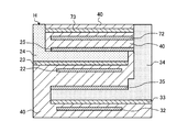
- the configuration of the photoelectric conversion layer 24 in the photoelectric conversion unit 20 is different from that of the embodiment. Specifically, similarly to the photoelectric conversion layer 34, the photoelectric conversion layer 24 of Modified Example 3 has a protruding region 24a that protrudes from the second electrode 25 in a plan view.
- the surface on the light incident side of the protruding region 24a is on the light incident side with respect to the portion of the photoelectric conversion layer 24 in contact with the second electrode 25 (that is, the portion other than the protruding region 24a of the photoelectric conversion layer 24). Is provided so as to project.
- the portion corresponding to the protruding region 24a can be used as an injection port through which a liquid raw material can be injected. That is, after forming the portion other than the photoelectric conversion layer 24 in the pixel array portion 10, the liquid raw material can be injected into the portion corresponding to the photoelectric conversion layer 24 through the injection port.
- the photoelectric conversion layer 24 can be formed by drying the liquid raw material injected into the portion corresponding to the photoelectric conversion layer 24 at a predetermined temperature. Therefore, according to the third modification, after the semiconductor process is completed to some extent, the photoelectric conversion layer 24 of the photoelectric conversion unit 20 can be formed in addition to the photoelectric conversion layer 34 of the photoelectric conversion unit 30. Detailed manufacturing steps of the pixel array section 10 according to the third modification will be described later.
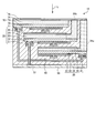
- FIG. 11 is a cross-sectional view schematically showing the structure of the pixel array unit 10 according to the modified example 4 of the embodiment of the present disclosure.
- the photoelectric conversion layer 24 of the photoelectric conversion unit 20 is provided with a protruding region 24a
- the photoelectric conversion layer 34 of the photoelectric conversion unit 30 is provided with a protruding region 34a.
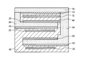
- another photoelectric conversion unit 70 is provided on the light incident side of the photoelectric conversion unit 20.
- the photoelectric conversion unit 70 is provided on the upper surface side of the photoelectric conversion unit 20 so as to be stacked on the photoelectric conversion unit 20.
- the photoelectric conversion unit 70 includes a first electrode 71, a charge storage electrode 72, a charge storage layer 73, a photoelectric conversion layer 74, and a second electrode 75.
- the first electrode 71 is provided in the photoelectric conversion unit 70 on the side opposite to the light incident side.
- the first electrode 71 has an upper surface in contact with the bottom surface of the charge storage layer 73.
- the first electrode 71 extends in the insulating layer 40 in the depth direction and is connected to the floating diffusion 53 provided in the semiconductor layer 50. That is, the first electrode 71 electrically connects the charge storage layer 73 and the floating diffusion 53.
- the first electrode 71 is made of a transparent conductor such as ITO, AZO, GZO, IZO.
- the constituent material of the first electrode 71 is not limited to these transparent conductors, and may be the same material as the various transparent conductors illustrated when the first electrode 21 is described.
- the charge storage electrode 72 is made of a transparent conductor such as ITO, AZO, GZO, and IZO.
- the constituent material of the charge storage electrode 72 is not limited to these transparent conductors, and may be the same as the various transparent conductors exemplified when the first electrode 21 is described.
- the charge storage electrode 72 is provided adjacent to the first electrode 71 via the insulating layer 40.
- the charge storage layer 73 is made of a semiconductor material having a large band gap, a high carrier mobility, and light transmittance.
- the constituent material of the charge storage tank 73 the same material as the various semiconductor materials exemplified in the description of the charge storage layer 23 can be used.
- the upper surface of the charge storage layer 73 is in contact with the bottom surface of the photoelectric conversion layer 74, and the bottom surface of the charge storage layer 73 is in contact with the upper surface of the first electrode 71.
- the bottom surface of the charge storage layer 73 is adjacent to the charge storage electrode 72 with the insulating layer 40 interposed therebetween. Then, when a predetermined voltage is applied to the charge storage electrode 72, the charge photoelectrically converted by the photoelectric conversion layer 74 is accumulated in the charge storage layer 73.
- the photoelectric conversion layer 74 is provided so as to cover the upper surface of the charge storage layer 73.
- the photoelectric conversion layer 74 is made of an organic semiconductor, and performs photoelectric conversion of light having a wavelength (for example, red) selected from the light L incident from the outside.
- the photoelectric conversion layer 74 preferably contains one or both of a p-type organic semiconductor and an n-type organic semiconductor.
- a p-type organic semiconductor and an n-type organic semiconductor the same materials as the various materials exemplified in the description of the photoelectric conversion layer 24 can be used.
- red light is photoelectrically converted by the photoelectric conversion layer 74
- a phthalocyanine dye, a subphthalocyanine dye (subphthalocyanine derivative), or the like can be used for the photoelectric conversion layer 74.
- the second electrode 75 is provided in contact with the upper surface of the photoelectric conversion layer 74.
- the second electrode 75 is made of a transparent conductor such as ITO, AZO, GZO, and IZO.
- the constituent material of the second electrode 75 is not limited to these transparent conductors, and may be the same material as the various transparent conductors exemplified when the first electrode 21 is described.
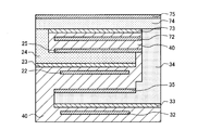
- the photoelectric conversion unit 70 having the photoelectric conversion layer 74 made of the organic semiconductor material is further laminated on the photoelectric conversion unit 20 and the photoelectric conversion unit 30 in one unit pixel 11. ..
- FIG. 12 is a circuit diagram showing a circuit configuration of the unit pixel 11 according to Modification 4 of the embodiment of the present disclosure.
- the unit pixel 11 has a floating diffusion 53, a reset transistor 63R, an amplification transistor 63A, and a selection transistor 63S as a circuit for reading out electric charges from the photoelectric conversion unit 70.
- a plurality of photoelectric conversion units 70 may share the floating diffusion 53. This eliminates the need to provide individual floating diffusion 53s in all the photoelectric conversion units 70, so that the circuit configuration in the pixel array unit 10 can be simplified.
- the manufacturing cost of the pixel array section 10 can be reduced.
- FIG. 13 is a cross-sectional view schematically showing the structure of the pixel array section 10 according to Modification Example 5 of the embodiment of the present disclosure.
- the manufacturing cost of the pixel array section 10 can be reduced.
- the photoelectric conversion layers 24, 34, and 74 are composed of a single layer, but when the photoelectric conversion layers 24, 34, and 74 are composed of a single layer,
- the structure is not limited, and may have a multilayer structure.
- the photoelectric conversion layers 24, 34, 74 prevent the injection of electrons from the second electrodes 25, 35, 75 into the light incident side of the light incident layer in addition to the layer that photoelectrically converts the light L. You may have an electron injection prevention layer.
- the photoelectric conversion layers 24, 34, and 74 may have an electron transport layer for transporting electrons on the side opposite to the light incident side of the photoelectric conversion layer in addition to the layer for photoelectric conversion of light L. Good. Further, the photoelectric conversion layers 24, 34, and 74 may have both the above-mentioned electron injection prevention layer and the electron transport layer in addition to the layer that photoelectrically converts light L.
- the unit pixel 11 is provided with three layers of a photoelectric conversion unit and a photodiode is shown, but the photoelectric conversion unit and the photodiode provided in the unit pixel 11 are limited to three layers. Alternatively, it may have one layer, two layers, or four or more layers.
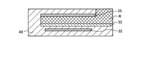
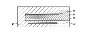
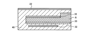
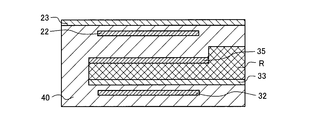
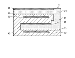
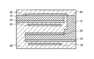
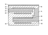
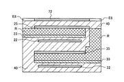
- FIGS. 14A to 22 are cross-sectional views schematically showing one manufacturing process of the pixel array unit 10 according to the embodiment of the present disclosure.
- the semiconductor layer 50 (see FIG. 2) is omitted for easy understanding. Further, in the semiconductor layer 50, the photodiode 60 shown in FIG. 4, various pixel transistors, various wirings, floating diffusions 51 to 53, and the like are already formed.
- the insulating layer 40 is formed on the surface of the semiconductor layer 50 (see FIG. 2), and the first electrode 31 (see FIG. 2) (not shown) and the charge storage are used inside the insulating layer 40.
- the electrode 32 is formed.
- the charge storage layer 33 is formed on the surface of the insulating layer 40 so as to cover the first electrode 31 and the insulating layer 40.
- the charge storage layer 33 is provided so as to be in contact with the surface of the first electrode 21 and adjacent to the charge storage electrode 22 via the insulating layer 40.
- a method for forming the insulating layer 40, the first electrode 31, and the charge storage electrode 32 conventionally known methods can be appropriately adopted. Note that, for ease of understanding, the illustration of the first electrode 31 is omitted in the following drawings.
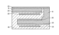
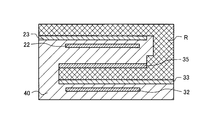
- the removal material R and the second electrode 35 are sequentially formed on the surface of the charge storage layer 33.
- the removal material R is provided at a position corresponding to the photoelectric conversion layer 34 in the pixel array section 10.
- the removal material R is a material that can be removed by a predetermined treatment, and is, for example, a resist material that can be removed by chemical etching.
- the removal material R is not limited to the resist material, and may be another material as long as it can be removed by a predetermined treatment.
- a method of forming the removal material R and the second electrode 35 a conventionally known method can be appropriately adopted.
- predetermined regions in the second electrode 35, the removal material R, and the charge storage layer 33 are etched by a conventionally known method to form the etching region E1.
- the etching region E1 is filled and the insulating layer 40 is formed so as to cover the surface of the second electrode 35.
- a predetermined region in the insulating layer 40, the second electrode 35, and the removal material R is etched by a conventionally known method to form an etching region E2.
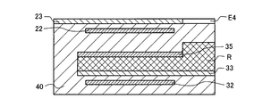
- the etching region E2 is formed at a position corresponding to the protruding region 34a in the pixel array portion 10 so as not to penetrate the removal material R.
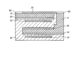
- the etching region E2 is filled and the removal material R is formed so as to cover the surface of the insulating layer 40.
- the removal material R is removed so that the surface of the insulating layer 40 and the surface of the removal material R are substantially flush with each other.
- the insulating layer 40 is formed so as to cover the surface of the insulating layer 40 and the surface of the removing material R.
- the charge storage electrode 22 is formed so as to cover the surface of the insulating layer 40.
- a predetermined region of the charge storage electrode 22 is etched by a conventionally known method to form an etching region E3.
- the etching region E3 is filled and the insulating layer 40 is formed so as to cover the surface of the charge storage electrode 22.
- the charge storage layer 23 is formed so as to cover the surface of the insulating layer 40.
- the first electrode 21 (see FIG. 2) of the photoelectric conversion unit 20 is also formed in parallel, but the process of forming the first electrode 21 is not shown or described. ..
- a predetermined region in the charge storage layer 23 is etched by a conventionally known method to form an etching region E4.
- the etching region E4 is filled and the insulating layer 40 is formed so as to cover the surface of the charge storage layer 23.
- a predetermined region in the insulating layer 40 is etched by a conventionally known method to form an etching region E5.
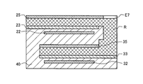
- the etching region E5 is formed so as to reach the removal material R formed so as to project toward the light incident side.
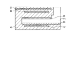
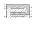
- the removal material R is formed so as to fill the etching region E5. Then, as shown in FIG. 14Q, the removal material R is removed by a predetermined treatment (for example, chemical etching), and a void V1 is formed in the region where the removal material R is provided.
- a predetermined treatment for example, chemical etching
- the annealing treatment is performed at a predetermined temperature with the void V1 shown in FIG. 14Q formed.
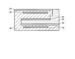
- the liquid raw material of the photoelectric conversion layer 34 is injected so as to fill the void V1 through the injection port H opened upward from the void V1. Then, by drying the liquid raw material injected into the void V1 at a predetermined temperature, the photoelectric conversion layer 34 is formed in the void V1.
- the photoelectric conversion layer 34 is formed between the charge storage layer 33 and the second electrode 35 in the embodiment. be able to.
- the insulating layer 40 and the photoelectric conversion layer 34 are conventionally known so that the surface of the charge storage layer 23, the surface of the insulating layer 40, and the surface of the photoelectric conversion layer 34 are substantially flush with each other. It is removed by the method of.
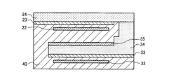
- the photoelectric conversion layer 24 is formed by a conventionally known method so as to cover the surfaces of the charge storage layer 23, the insulating layer 40, and the photoelectric conversion layer 34.
- the surface of the charge storage layer 23, the insulating layer 40, and the photoelectric conversion layer 34 is coated with the liquid raw material of the photoelectric conversion layer 24, and the liquid raw material is dried at a predetermined temperature to cause the photoelectric conversion layer 24. Is formed.
- the process for forming the photoelectric conversion layer 24 is not limited to the above-mentioned method, and may be another method such as a vapor phase growth method.
- the second electrode 25 is formed by a conventionally known method so as to cover the surface of the photoelectric conversion layer 24, and the manufacturing process of the pixel array section 10 according to the embodiment is completed.
- 15A to 15E are cross-sectional views schematically showing one manufacturing process of the pixel array section 10 according to Modification Example 1 of the embodiment of the present disclosure. Since the process up to the middle of the modification 1 is the same as the process shown in FIGS. 14A to 14Q, the description thereof will be omitted.
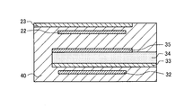
- annealing treatment is performed at a predetermined temperature with the void V1 formed. Then, as shown in FIG. 15A, the liquid raw material of the photoelectric conversion layer 34 is injected through the injection port H opening upward from the void V1 so that the void V1 is not filled.
- the photoelectric conversion layer 34 is formed in the void V1 by drying the liquid raw material injected into the void V1 at a predetermined temperature. Since the liquid raw material of the photoelectric conversion layer 34 is injected so that the void V1 is not filled, a part of the void V1 remains as the void V1a.
- the gap V1a is filled and the insulating layer 40 is formed so as to cover the surface of the insulating layer 40.
- the insulating layer 40 is removed by a conventionally known method so that the surface of the charge storage layer 23 and the surface of the insulating layer 40 are substantially flush with each other.
- the photoelectric conversion layer 24 is formed by a conventionally known method so as to cover the surfaces of the charge storage layer 23 and the insulating layer 40.
- the second electrode 25 is formed by a conventionally known method so as to cover the surface of the photoelectric conversion layer 24, and the manufacturing process of the pixel array section 10 according to the modified example 1 of the embodiment is performed. finish.
- 16A to 16E are cross-sectional views schematically showing one manufacturing process of the pixel array section 10 according to Modification 2 of the embodiment of the present disclosure. Since the process up to the middle of the modification 2 is the same as the process shown in FIGS. 14A to 14Q, the description thereof will be omitted.
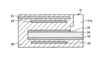
- annealing treatment is performed at a predetermined temperature with the void V1 formed. Then, as shown in FIG. 16A, the liquid raw material of the photoelectric conversion layer 34 is formed so that the bottom surface of the second electrode 35 and the liquid surface are substantially flush with each other via the injection port H opening upward from the void V1. Infused.
- the photoelectric conversion layer 34 is formed in the void V1 by drying the liquid raw material injected into the void V1 at a predetermined temperature. Since the liquid raw material of the photoelectric conversion layer 34 is injected such that the bottom surface of the second electrode 35 and the liquid surface are substantially flush with each other, part of the void V1 remains as the void V1b.
- the gap V1b is filled and the insulating layer 40 is formed so as to cover the surface of the insulating layer 40.
- the insulating layer 40 is removed so that the surface of the charge storage layer 23 and the surface of the insulating layer 40 are substantially flush with each other.
- the photoelectric conversion layer 24 is formed so as to cover the surfaces of the charge storage layer 23 and the insulating layer 40.
- the second electrode 25 is formed so as to cover the surface of the photoelectric conversion layer 24, and the manufacturing process of the pixel array unit 10 according to the second modification of the embodiment is completed.
- 17A to 17I are cross-sectional views schematically showing one manufacturing process of the pixel array section 10 according to Modification 3 of the embodiment of the present disclosure. Since the process up to the middle of the modification 3 is the same as the process shown in FIGS. 14A to 14P, the description thereof will be omitted.
- the insulating layer 40 and the removal are removed so that the surface of the charge storage layer 23, the surface of the insulating layer 40, and the surface of the removal material R are substantially flush with each other. Material R is removed. Further, the insulating layer 40 is formed on the surface of the insulating layer 40 provided between the charge storage layer 23 and the removal material R.
- the removal material R is formed so as to cover the surface of the charge storage layer 23 and the surface of the removal material R so that the surface of the insulation layer 40 and the surface of the removal material R are substantially flush with each other.
- the second electrode 25 is formed so as to cover the surfaces of the removal material R and the insulating layer 40.
- a predetermined region of the second electrode 25 is etched by a conventionally known method to form an etching region E6.
- the etching region E6 is provided so as to expose the removal material R formed on the surface of the charge storage layer 23 and the removal material R formed on the surface of the charge storage layer 33, respectively.
- the removal material R is removed by a predetermined process (for example, chemical etching), and voids V2 and V3 are formed in the region where the removal material R was provided.
- the void V2 is a void formed between the charge storage layer 33 and the second electrode 35
- the void V3 is a void formed between the charge storage layer 23 and the second electrode 25.
- the annealing treatment is performed at a predetermined temperature with the voids V2 and V3 shown in FIG. 17E formed.
- the mask M1 is formed so as to close the opening of the void V3.
- the mask M1 is, for example, a metal mask and is formed by a conventionally known method.
- the liquid raw material of the photoelectric conversion layer 34 is injected so as to fill the void V2 through the inlet H that opens upward from the void V2. Then, the photoelectric conversion layer 34 is formed in the void V2 by drying the liquid raw material injected into the void V2 at a predetermined temperature. Then, as shown in FIG. 17H, the mask M1 is removed by a conventionally known method.
- the liquid raw material of the photoelectric conversion layer 24 is injected so as to fill the void V3 through the injection port H opened upward from the void V3. Finally, the liquid raw material injected into the void V3 is dried at a predetermined temperature to form the photoelectric conversion layer 24 in the void V3, and thus the pixel array section 10 according to Modification 3 of the embodiment. The manufacturing process is completed.
- the annealing process is performed in the state shown in FIG. 17E is shown, but the annealing process is not limited to the case shown in FIG. 17E and the state shown in FIG. It may be done in.
- FIGS. 14A to 14P are cross-sectional views schematically showing one manufacturing process of the pixel array section 10 according to another example of Modification 3 of the embodiment of the present disclosure. Since the steps up to the middle in this other example are the same as the steps shown in FIGS. 14A to 14P, the description thereof will be omitted.
- the insulating layer 40 and the removal are removed so that the surface of the charge storage layer 23, the surface of the insulating layer 40 and the surface of the removal material R are substantially flush with each other. Material R is removed. Further, the removing material R is formed so as to cover the surface of the charge storage layer 23, the surface of the insulating layer 40, and the surface of the removing material R.
- the second electrode 25 is formed so as to cover the surface of the removal material R. Then, as shown in FIG. 18C, a predetermined region of the second electrode 25 is etched to form an etching region E7. The etching region E7 is provided so that the removal material R is exposed.
- the removal material R is removed by a predetermined process (for example, chemical etching), and the void V4 is formed in the region where the removal material R was provided.
- the annealing treatment is performed at a predetermined temperature with the void V4 shown in FIG. 18D formed.
- the liquid raw material of the photoelectric conversion layer 34 is provided so that the upper surface of the charge storage layer 23 and the liquid surface are substantially flush with each other through the injection port H that opens upward from the void V4. Is injected. Then, by drying the liquid raw material injected into the void V4 at a predetermined temperature, the photoelectric conversion layer 34 is formed in the void V4.
- the liquid raw material of the photoelectric conversion layer 34 is injected so that the upper surface of the charge storage layer 23 and the liquid surface are substantially flush with each other, a part of the void V4 remains as the void V4a.
- the upper surface of the charge storage layer 23 and the upper surface of the photoelectric conversion layer 34 do not have to be substantially flush with each other.
- the liquid raw material of the photoelectric conversion layer 24 is injected so as to fill the void V4a through the injection port H opened upward from the void V4a.
- the photoelectric conversion layer 24 is formed in the void V4a, and the pixel array portion 10 according to another example of the modified example 3 is formed. Manufacturing process is completed.
- 19A to 19L are cross-sectional views schematically showing one manufacturing process of the pixel array section 10 according to Modification 4 of the embodiment of the present disclosure. Since the steps up to the middle of Modification 4 are the same as the steps shown in FIGS. 14A to 14P and FIGS. 17A to 17D, description thereof will be omitted.
- the etching region E6 is filled and the insulating layer 40 is formed so as to cover the surface of the second electrode 35.
- the charge storage electrode 72 is formed so as to cover the surface of the insulating layer 40.
- a predetermined region of the charge storage electrode 72 is etched by a conventionally known method to form an etching region E8.
- the etching region E8 is filled and the insulating layer 40 is formed so as to cover the surface of the charge storage electrode 72.
- the charge storage layer 73 is formed so as to cover the surface of the insulating layer 40, and the insulating layer 40 is formed so as to cover the surface of the charge storage layer 73.
- the first electrode 71 (see FIG. 11) of the photoelectric conversion unit 70 is also formed in parallel, but the process of forming the first electrode 71 is not shown or described. ..
- predetermined regions in the insulating layer 40 and the charge storage layer 73 are etched by a conventionally known method to form an etching region E9.
- the etching region E9 is provided so as to expose the removal material R formed on the surface of the charge storage layer 23 and the removal material R formed on the surface of the charge storage layer 33, respectively.
- the removal material R is removed by a predetermined treatment (for example, chemical etching), and voids V5 and V6 are formed in the region where the removal material R is provided.
- the gap V5 is a gap formed between the charge storage layer 33 and the second electrode 35
- the gap V6 is a gap formed between the charge storage layer 23 and the second electrode 25.
- the annealing treatment is performed at a predetermined temperature with the voids V5 and V6 shown in FIG. 19G formed.
- the mask M2 is formed so as to close the opening of the void V6.
- the mask M2 is, for example, a metal mask and is formed by a conventionally known method.
- the liquid raw material of the photoelectric conversion layer 34 is injected so as to fill the void V5 through the injection port H that opens upward from the void V5.
- the photoelectric conversion layer 34 is formed in the void V5 by drying the liquid raw material injected into the void V5 at a predetermined temperature.
- the mask M1 is removed by a conventionally known method. Then, the liquid raw material of the photoelectric conversion layer 24 is injected so as to fill the void V6 through the injection port H that opens upward from the void V6.
- the photoelectric conversion layer 24 is formed in the void V6 by drying the liquid raw material injected into the void V6 at a predetermined temperature.
- the insulating layer 40, the photoelectric conversion layer 24, and the photoelectric are so that the surface of the charge storage layer 73, the surface of the photoelectric conversion layer 24, and the surface of the photoelectric conversion layer 34 are substantially flush with each other.
- the conversion layer 34 is removed.
- a photoelectric conversion layer 74 is formed by a conventionally known method so as to cover the surfaces of the charge storage layer 73, the photoelectric conversion layer 24, and the photoelectric conversion layer 34.
- the liquid raw material of the photoelectric conversion layer 74 is applied to the surfaces of the charge storage layer 73, the photoelectric conversion layer 24, and the photoelectric conversion layer 34, and the liquid raw material is dried at a predetermined temperature to obtain the photoelectric conversion layer. 74 is formed.
- the process of forming the photoelectric conversion layer 74 is not limited to the above-mentioned method, and may be another method such as a vapor phase growth method.
- the second electrode 75 is formed by a conventionally known method so as to cover the surface of the photoelectric conversion layer 74, and the manufacturing process of the pixel array section 10 according to the embodiment is completed.
- FIG. 20 is a plan view schematically showing an example of the arrangement of the injection ports H according to the embodiment of the present disclosure. As shown in FIG. 20, in the above-mentioned manufacturing process, an injection port H for injecting a liquid raw material such as a photoelectric conversion layer 34 may be provided for each unit pixel 11.
- FIG. 21 is a plan view schematically showing an example of the arrangement of the injection ports H according to the embodiment of the present disclosure.
- the injection port H for injecting the liquid raw material such as the photoelectric conversion layer 34 may be provided for each of the plurality (four in the example of FIG. 21) of the unit pixels 11.
- FIG. 22 is a plan view schematically showing an example of the arrangement of the injection ports H according to the embodiment of the present disclosure.
- the injection port H for injecting the liquid raw material such as the photoelectric conversion layer 34 has such a pixel group outside the pixel group composed of the plurality of unit pixels 11 arranged in a matrix. It may be provided so as to surround it.
- FIG. 23 is a flowchart showing the processing procedure of the manufacturing process according to the embodiment.
- the first electrode 31 is formed on the surface of the semiconductor layer 50 on which the photodiode 60, various pixel transistors, various wirings, floating diffusions 51 to 53, and the like have already been formed (step S101).
- the first electrode 31 is electrically connected to the floating diffusion 52, and the periphery thereof is covered with the insulating layer 40.
- the removal material R is formed above the first electrode 31 (step S102).
- the removal material R is formed on the surface of the charge storage layer 33 formed so as to be in contact with the surface of the first electrode 31.
- the removal material R may be directly formed on the surface of the first electrode 31.
- the second electrode 35 is formed on the surface of the removal material R (step S103).
- the step of forming the second electrode 35 may be performed so as not to cover a part of the removal material R.
- the removal material R may be provided so that the second electrode 35 can be partially removed in plan view.
- the removal material R is removed by a predetermined process (for example, chemical etching) (step S104).
- a predetermined process for example, chemical etching
- annealing is performed at a predetermined temperature with the void V1 formed (step S105).
- the annealing step may be performed at a desired temperature higher than the heat resistant temperature of the photoelectric conversion layer 34 formed in the subsequent step S106.
- the photoelectric conversion layer 34 is formed in the region (void V1) from which the removal material R has been removed (step S106), and the process is completed.
- the step of forming the photoelectric conversion layer 34 may be performed by injecting the liquid raw material of the photoelectric conversion layer 34 into the void V1 from the injection port H formed so as to remove the second electrode 35.
- the photoelectric conversion layer 34 can be formed after the semiconductor process is completed to some extent.
- the solid-state imaging device 1 includes the first electrode 31, the photoelectric conversion layer 34 electrically connected to the first electrode 31, and the second electrode 35 provided on the light incident side surface of the photoelectric conversion layer 34.
- the photoelectric conversion unit 30 having the above is provided. Further, the photoelectric conversion layer 34 has a protruding region 34a that protrudes from the second electrode 35 in a plan view.
- the photoelectric conversion unit 30 is provided with a charge storage layer 33 provided on a surface of the photoelectric conversion layer 34 opposite to the light incident side, and a charge storage layer via an insulating layer 40. 33, and a charge storage electrode 32 disposed so as to face 33.
- the reset noise due to the reset transistor 62R during the reset operation can be reduced, so that a high-quality image can be acquired.
- a plurality of photoelectric conversion units 30 are provided. Further, the plurality of photoelectric conversion units 30 share one floating diffusion 52.
- the protruding region 34a of the photoelectric conversion layer 34 is substantially flush with the portion of the photoelectric conversion layer 34 in contact with the second electrode 35 on the light incident side.
- the photoelectric conversion layer 34 can be formed after the semiconductor process is completed to some extent.
- the protruding region 34 a of the photoelectric conversion layer 34 has a surface on the light incident side protruding from a portion of the photoelectric conversion layer 34 in contact with the second electrode 35.
- the photoelectric conversion layer 34 can be formed after the semiconductor process is completed to some extent.
- the photoelectric conversion layer 34 of the photoelectric conversion unit 30 is made of an organic semiconductor material.
- the photoelectric conversion unit 30 can suppress the attenuation of the light L, so that a high-quality image can be acquired.
- the solid-state imaging device 1 further includes another photoelectric conversion unit 20 that is provided on the light incident side of the photoelectric conversion unit 30 and photoelectrically converts light having a wavelength different from that of the photoelectric conversion unit 30.
- the photoelectric conversion layer 24 of another photoelectric conversion unit 20 is made of an organic semiconductor material.
- the photoelectric conversion unit 20 can suppress the attenuation of the light L, so that a high-quality image can be acquired.
- a step of forming the first electrode 31, a step of forming the removal material R, a step of forming the second electrode 35, and a step of removing the removal material E are removed.
- the process includes a step and a step of forming the photoelectric conversion layer 34.
- the removal material R is formed above the first electrode 31.
- the second electrode 35 is formed on the surface of the removal material R.
- the photoelectric conversion layer 34 is formed in the region where the removal material R is removed.
- the method for manufacturing the solid-state image sensor 1 includes a step of annealing at a predetermined temperature before the step of forming the photoelectric conversion layer 34.
- the annealing step is annealing at a temperature higher than the heat resistant temperature of the photoelectric conversion layer 34.
- the step of forming the photoelectric conversion layer 34 includes liquid in the region where the removal material R is removed from the injection port H formed so as to exclude the second electrode 35. It is carried out by injecting a raw material in the shape of a circle.
- the photoelectric conversion layer 34 can be formed after the semiconductor process is completed to some extent.
- the present disclosure is not limited to the application to the solid-state imaging device. That is, the present disclosure is applicable to general electronic devices including a solid-state imaging device, such as a camera module, an imaging device, a mobile terminal device having an imaging function, or a copying machine using the solid-state imaging device in an image reading unit. Is applicable.
- a solid-state imaging device such as a camera module, an imaging device, a mobile terminal device having an imaging function, or a copying machine using the solid-state imaging device in an image reading unit. Is applicable.
- imaging devices include digital still cameras and video cameras.
- mobile terminal device having such an imaging function examples include a smartphone and a tablet type terminal.
- FIG. 24 is a block diagram showing a configuration example of an imaging device as the electronic device 100 to which the technology according to the present disclosure is applied.
- the electronic device 100 of FIG. 24 is, for example, an electronic device such as an imaging device such as a digital still camera or a video camera, or a mobile terminal device such as a smartphone or a tablet terminal.
- the electronic device 100 includes a lens group 101, a solid-state imaging device 102, a DSP circuit 103, a frame memory 104, a display unit 105, a recording unit 106, an operation unit 107, and a power supply unit 108. It is composed.
- the DSP circuit 103, the frame memory 104, the display unit 105, the recording unit 106, the operation unit 107, and the power supply unit 108 are connected to each other via a bus line 109.
- the lens group 101 captures incident light (image light) from a subject and forms an image on the imaging surface of the solid-state imaging device 102.
- the solid-state image pickup device 102 corresponds to the solid-state image pickup device 1 according to the above-described embodiment, and converts the light amount of incident light imaged on the image pickup surface by the lens group 101 into an electric signal for each pixel and outputs the electric signal as a pixel signal. To do.
- the DSP circuit 103 is a camera signal processing circuit that processes a signal supplied from the solid-state imaging device 102.
- the frame memory 104 temporarily holds the image data processed by the DSP circuit 103 in frame units.
- the display unit 105 is composed of a panel-type display device such as a liquid crystal panel or an organic EL (Electro Luminescence) panel, and displays a moving image or a still image captured by the solid-state image sensor 102.
- the recording unit 106 records image data of a moving image or a still image captured by the solid-state image sensor 102 on a recording medium such as a semiconductor memory or a hard disk.
- the operation unit 107 issues operation commands for various functions of the electronic device 100 according to the operation by the user.
- the power supply unit 108 appropriately supplies various power sources that serve as operating power sources for the DSP circuit 103, the frame memory 104, the display unit 105, the recording unit 106, and the operation unit 107 to these supply targets.
- the occurrence of color mixing can be suppressed by applying the solid-state image sensor 1 of each of the above-described embodiments as the solid-state image sensor 102.
- the technology according to the present disclosure (this technology) can be applied to various products.
- the technology according to the present disclosure is realized as a device mounted on a moving body of any kind such as an automobile, an electric vehicle, a hybrid electric vehicle, a motorcycle, a bicycle, a personal mobility, an airplane, a drone, a ship, and a robot. May be.
- FIG. 25 is a block diagram showing a schematic configuration example of a vehicle control system, which is an example of a mobile control system to which the technology according to the present disclosure can be applied.
- the vehicle control system 12000 includes a plurality of electronic control units connected via a communication network 12001.
- the vehicle control system 12000 includes a drive system control unit 12010, a body system control unit 12020, a vehicle exterior information detection unit 12030, a vehicle interior information detection unit 12040, and an integrated control unit 12050.
- a microcomputer 12051 As a functional configuration of the integrated control unit 12050, a microcomputer 12051, a voice image output unit 12052, and an in-vehicle network I/F (Interface) 12053 are shown.
- the drive system control unit 12010 controls the operation of devices related to the drive system of the vehicle according to various programs.
- the drive system control unit 12010 provides a driving force generator for generating the driving force of the vehicle such as an internal combustion engine or a driving motor, a driving force transmission mechanism for transmitting the driving force to the wheels, and a steering angle of the vehicle. It functions as a steering mechanism for adjustment and a control device such as a braking device that generates a braking force of the vehicle.
- the body system control unit 12020 controls the operation of various devices mounted on the vehicle body according to various programs.
- the body system control unit 12020 functions as a keyless entry system, a smart key system, a power window device, or a control device for various lamps such as headlamps, back lamps, brake lamps, blinkers or fog lamps.
- the body system control unit 12020 may be input with radio waves transmitted from a portable device that substitutes for the key or signals of various switches.
- the body system control unit 12020 receives inputs of these radio waves or signals and controls a vehicle door lock device, a power window device, a lamp, and the like.
- the vehicle exterior information detection unit 12030 detects information outside the vehicle equipped with the vehicle control system 12000.
- the imaging unit 12031 is connected to the vehicle outside information detection unit 12030.
- the vehicle outside information detection unit 12030 causes the image pickup unit 12031 to capture an image of the outside of the vehicle and receives the captured image.
- the vehicle exterior information detection unit 12030 may perform object detection processing or distance detection processing such as people, vehicles, obstacles, signs, or characters on the road surface based on the received image.
- the imaging unit 12031 is an optical sensor that receives light and outputs an electric signal according to the amount of the light received.
- the imaging unit 12031 can output the electric signal as an image or as distance measurement information.
- the light received by the imaging unit 12031 may be visible light or invisible light such as infrared light.
- the in-vehicle information detection unit 12040 detects in-vehicle information.
- a driver state detection unit 12041 that detects the state of the driver is connected.
- the driver state detection unit 12041 includes, for example, a camera that images the driver, and the in-vehicle information detection unit 12040 determines the degree of fatigue or concentration of the driver based on the detection information input from the driver state detection unit 12041. It may be calculated or it may be determined whether the driver is asleep.
- the microcomputer 12051 calculates the control target value of the driving force generator, the steering mechanism, or the braking device based on the information inside and outside the vehicle acquired by the vehicle exterior information detection unit 12030 or the vehicle interior information detection unit 12040, and the drive system control unit.
- a control command can be output to 12010.
- the microcomputer 12051 realizes the functions of ADAS (Advanced Driver Assistance System) that includes collision avoidance or impact mitigation of a vehicle, follow-up traveling based on an inter-vehicle distance, vehicle speed maintenance traveling, a vehicle collision warning, or a vehicle lane departure warning. It is possible to perform cooperative control for the purpose.
- ADAS Advanced Driver Assistance System
- the microcomputer 12051 controls the driving force generator, the steering mechanism, the braking device, and the like based on the information around the vehicle acquired by the vehicle exterior information detection unit 12030 or the vehicle interior information detection unit 12040. It is possible to perform cooperative control for the purpose of autonomous driving or the like that autonomously travels without depending on operation.
- the microcomputer 12051 can output a control command to the body system control unit 12020 based on the information outside the vehicle acquired by the outside information detection unit 12030.
- the microcomputer 12051 controls the headlamps according to the position of the preceding vehicle or the oncoming vehicle detected by the external information detection unit 12030, and performs cooperative control for the purpose of antiglare such as switching the high beam to the low beam. It can be carried out.
- the voice image output unit 12052 transmits an output signal of at least one of a voice and an image to an output device capable of visually or audibly notifying information to an occupant of the vehicle or the outside of the vehicle.
- an audio speaker 12061, a display unit 12062, and an instrument panel 12063 are exemplified as output devices.
- the display unit 12062 may include, for example, at least one of an onboard display and a head-up display.
- FIG. 26 is a diagram showing an example of the installation position of the imaging unit 12031.
- the imaging unit 12031 includes imaging units 12101, 12102, 12103, 12104, and 12105.
- the imaging units 12101, 12102, 12103, 12104, 12105 are provided at positions such as, for example, the front nose, side mirrors, rear bumpers, back doors, and the upper part of the windshield in the vehicle interior of the vehicle 12100.
- the image capturing unit 12101 provided on the front nose and the image capturing unit 12105 provided on the upper part of the windshield in the vehicle interior mainly acquire an image in front of the vehicle 12100.
- the image capturing units 12102 and 12103 provided in the side mirrors mainly acquire images of the side of the vehicle 12100.
- the imaging unit 12104 provided on the rear bumper or the back door mainly acquires an image of the rear of the vehicle 12100.
- the imaging unit 12105 provided on the upper part of the windshield in the vehicle interior is mainly used for detecting a preceding vehicle, a pedestrian, an obstacle, a traffic signal, a traffic sign, a lane, or the like.
- FIG. 26 shows an example of the shooting range of the imaging units 12101 to 12104.
- the imaging range 12111 indicates the imaging range of the imaging unit 12101 provided on the front nose
- the imaging ranges 12112 and 12113 indicate the imaging ranges of the imaging units 12102 and 12103 provided on the side mirrors
- the imaging range 12114 indicates The imaging range of the imaging part 12104 provided in a rear bumper or a back door is shown.
- a bird's-eye view image of the vehicle 12100 viewed from above can be obtained.
- At least one of the image capturing units 12101 to 12104 may have a function of acquiring distance information.
- at least one of the image capturing units 12101 to 12104 may be a stereo camera including a plurality of image capturing elements, or may be an image capturing element having pixels for phase difference detection.
- the microcomputer 12051 has a distance to each three-dimensional object within the imaging range 12111 to 12114 based on the distance information obtained from the imaging units 12101 to 12104, and a temporal change of this distance (relative velocity with respect to the vehicle 12100).
- a predetermined speed for example, 0 km / h or more.
- the microcomputer 12051 can set an inter-vehicle distance to be secured in front of the preceding vehicle in advance, and can perform automatic braking control (including follow-up stop control), automatic acceleration control (including follow-up start control), and the like. In this way, it is possible to perform cooperative control for the purpose of autonomous driving or the like that autonomously travels without depending on the operation of the driver.
- the microcomputer 12051 converts three-dimensional object data related to a three-dimensional object into two-wheeled vehicles, ordinary vehicles, large vehicles, pedestrians, electric poles, and other three-dimensional objects based on the distance information obtained from the imaging units 12101 to 12104. It can be classified and extracted and used for automatic avoidance of obstacles. For example, the microcomputer 12051 identifies an obstacle around the vehicle 12100 into an obstacle visible to the driver of the vehicle 12100 and an obstacle difficult to see. Then, the microcomputer 12051 determines the collision risk indicating the risk of collision with each obstacle, and when the collision risk is equal to or higher than the set value and there is a possibility of collision, the microcomputer 12051 via the audio speaker 12061 or the display unit 12062. By outputting an alarm to the driver and performing forced deceleration and avoidance steering via the drive system control unit 12010, driving support for collision avoidance can be provided.
- At least one of the imaging units 12101 to 12104 may be an infrared camera that detects infrared rays.
- the microcomputer 12051 can recognize a pedestrian by determining whether or not a pedestrian is present in the images captured by the imaging units 12101 to 12104.
- pedestrian recognition includes, for example, a procedure for extracting feature points in an image captured by an imaging unit 12101 to 12104 as an infrared camera, and pattern matching processing for a series of feature points indicating the outline of an object to determine whether or not the pedestrian is a pedestrian. Is performed by the procedure for determining.
- the audio image output unit 12052 When the microcomputer 12051 determines that a pedestrian is present in the captured images of the imaging units 12101 to 12104 and recognizes the pedestrian, the audio image output unit 12052 outputs a square contour line for emphasizing the recognized pedestrian.
- the display unit 12062 is controlled so as to superimpose and display. Further, the audio image output unit 12052 may control the display unit 12062 so as to display an icon or the like indicating a pedestrian at a desired position.
- the technology according to the present disclosure can be applied to the imaging unit 12031 among the configurations described above.
- the solid-state imaging device 1 of FIG. 1 can be applied to the imaging unit 12031.
- a high-quality image can be acquired from the imaging unit 12031.
- the technology according to the present disclosure (this technology) can be applied to various products.
- the technology according to the present disclosure may be applied to an endoscopic surgery system.
- FIG. 27 is a diagram showing an example of a schematic configuration of an endoscopic surgery system to which the technique according to the present disclosure (the present technique) can be applied.
- FIG. 27 illustrates a situation in which an operator (doctor) 11131 is operating on a patient 11132 on a patient bed 11133 using the endoscopic surgery system 11000.
- the endoscopic surgery system 11000 includes an endoscope 11100, other surgical tools 11110 such as a pneumoperitoneum tube 11111 and an energy treatment tool 11112, and a support arm device 11120 that supports the endoscope 11100.
- a cart 11200 equipped with various devices for endoscopic surgery.
- the endoscope 11100 is composed of a lens barrel 11101 into which a region having a predetermined length from the distal end is inserted into the body cavity of the patient 11132, and a camera head 11102 connected to the base end of the lens barrel 11101.
- the endoscope 11100 configured as a so-called rigid mirror having the rigid barrel 11101 is illustrated, but the endoscope 11100 may be configured as a so-called flexible mirror having a flexible barrel. Good.
- An opening in which an objective lens is fitted is provided at the tip of the lens barrel 11101.
- a light source device 11203 is connected to the endoscope 11100, and light generated by the light source device 11203 is guided to the tip of the lens barrel by a light guide extending inside the lens barrel 11101. It is irradiated toward the observation target in the body cavity of the patient 11132 through the lens.
- the endoscope 11100 may be a direct-viewing endoscope, or may be a perspective or side-viewing endoscope.
- An optical system and an image pickup device are provided inside the camera head 11102, and the reflected light (observation light) from the observation target is condensed on the image pickup device by the optical system.
- the observation light is photoelectrically converted by the imaging element, and an electric signal corresponding to the observation light, that is, an image signal corresponding to the observation image is generated.
- the image signal is transmitted to the camera control unit (CCU: Camera Control Unit) 11201 as RAW data.
- the CCU11201 is composed of a CPU (Central Processing Unit), a GPU (Graphics Processing Unit), etc., and comprehensively controls the operations of the endoscope 11100 and the display device 11202. Further, the CCU 11201 receives the image signal from the camera head 11102, and performs various image processing such as development processing (demosaic processing) on the image signal for displaying an image based on the image signal.
- image processing such as development processing (demosaic processing)
- the display device 11202 displays an image based on an image signal subjected to image processing by the CCU 11201 under the control of the CCU 11201.
- the light source device 11203 is composed of a light source such as an LED (light emitting diode), for example, and supplies irradiation light to the endoscope 11100 when photographing a surgical site or the like.
- a light source such as an LED (light emitting diode)
- the input device 11204 is an input interface for the endoscopic surgery system 11000.
- the user can input various information and input instructions to the endoscopic surgery system 11000 via the input device 11204.
- the user inputs an instruction to change the imaging conditions (type of irradiation light, magnification, focal length, etc.) by the endoscope 11100.
- the treatment tool control device 11205 controls the drive of the energy treatment tool 11112 for cauterizing, incising, sealing a blood vessel, or the like of a tissue.
- the pneumoperitoneum device 11206 is used to inflate the body cavity of the patient 11132 through the pneumoperitoneum tube 11111 in order to inflate the body cavity of the patient 11132 for the purpose of securing the visual field by the endoscope 11100 and the working space of the operator.
- the recorder 11207 is a device capable of recording various information related to surgery.
- the printer 11208 is a device that can print various types of information regarding surgery in various formats such as text, images, or graphs.
- the light source device 11203 that supplies the irradiation light to the endoscope 11100 when photographing the surgical site can be composed of, for example, an LED, a laser light source, or a white light source composed of a combination thereof.
- a white light source is configured by combining RGB laser light sources, the output intensity and output timing of each color (each wavelength) can be controlled with high accuracy. Therefore, the light source device 11203 adjusts the white balance of the captured image. It can be carried out.
- the laser light from each of the RGB laser light sources is irradiated to the observation target in a time-division manner, and the drive of the image sensor of the camera head 11102 is controlled in synchronization with the irradiation timing to support each of RGB. It is also possible to capture the image in a time-division manner. According to this method, a color image can be obtained without providing a color filter on the image sensor.
- the drive of the light source device 11203 may be controlled so as to change the intensity of the output light at predetermined time intervals.
- the drive of the image sensor of the camera head 11102 in synchronization with the timing of changing the light intensity to acquire an image in a time-division manner and synthesizing the image, so-called high dynamic without blackout and overexposure. Images of the range can be generated.
- the light source device 11203 may be configured to be able to supply light in a predetermined wavelength band corresponding to special light observation.
- the special light observation for example, by utilizing the wavelength dependence of the absorption of light in body tissues, the mucosal surface layer is irradiated by irradiating a narrow band of light as compared with the irradiation light (that is, white light) during normal observation.
- a so-called narrow band imaging is performed to capture a specific tissue such as blood vessels with high contrast.
- fluorescence observation in which an image is obtained by the fluorescence generated by irradiating the excitation light may be performed.
- the light source device 11203 may be configured to be capable of supplying narrow band light and / or excitation light corresponding to such special light observation.
- FIG. 28 is a block diagram showing an example of the functional configuration of the camera head 11102 and CCU 11201 shown in FIG.
- the camera head 11102 includes a lens unit 11401, an imaging unit 11402, a driving unit 11403, a communication unit 11404, and a camera head control unit 11405.
- CCU11201 has a communication unit 11411, an image processing unit 11412, and a control unit 11413.
- the camera head 11102 and CCU11201 are communicatively connected to each other by a transmission cable 11400.
- the lens unit 11401 is an optical system provided at a connection portion with the lens barrel 11101.
- the observation light taken in from the tip of the lens barrel 11101 is guided to the camera head 11102 and enters the lens unit 11401.
- the lens unit 11401 is configured by combining a plurality of lenses including a zoom lens and a focus lens.
- the image sensor constituting the image pickup unit 11402 may be one (so-called single plate type) or a plurality (so-called multi-plate type).
- each image pickup element may generate an image signal corresponding to each of RGB, and a color image may be obtained by synthesizing them.
- the image pickup unit 11402 may be configured to have a pair of image pickup elements for acquiring image signals for the right eye and the left eye corresponding to 3D (dimensional) display, respectively.
- the 3D display enables the operator 11131 to more accurately grasp the depth of the biological tissue in the surgical site.
- a plurality of lens units 11401 may be provided corresponding to each image pickup element.
- the image pickup unit 11402 does not necessarily have to be provided in the camera head 11102.
- the imaging unit 11402 may be provided inside the lens barrel 11101 immediately after the objective lens.
- the drive unit 11403 is composed of an actuator, and moves the zoom lens and the focus lens of the lens unit 11401 by a predetermined distance along the optical axis under the control of the camera head control unit 11405. Accordingly, the magnification and focus of the image captured by the image capturing unit 11402 can be adjusted as appropriate.
- the communication unit 11404 is composed of a communication device for transmitting/receiving various information to/from the CCU 11201.
- the communication unit 11404 transmits the image signal obtained from the image pickup unit 11402 as RAW data to the CCU 11201 via the transmission cable 11400.
- the communication unit 11404 receives a control signal for controlling the drive of the camera head 11102 from the CCU 11201 and supplies the control signal to the camera head control unit 11405.
- the control signal includes, for example, information to specify the frame rate of the captured image, information to specify the exposure value at the time of imaging, and / or information to specify the magnification and focus of the captured image. Contains information about the condition.
- the image capturing conditions such as the frame rate, the exposure value, the magnification, and the focus may be appropriately designated by the user, or may be automatically set by the control unit 11413 of the CCU 11201 based on the acquired image signal. Good. In the latter case, so-called AE (Auto Exposure) function, AF (Auto Focus) function, and AWB (Auto White Balance) function are installed in the endoscope 11100.
- AE Auto Exposure
- AF Auto Focus
- AWB Auto White Balance
- the camera head control unit 11405 controls the driving of the camera head 11102 based on the control signal from the CCU 11201 received via the communication unit 11404.
- the communication unit 11411 is composed of a communication device for transmitting and receiving various information to and from the camera head 11102.
- the communication unit 11411 receives the image signal transmitted from the camera head 11102 via the transmission cable 11400.
- the communication unit 11411 transmits a control signal for controlling the driving of the camera head 11102 to the camera head 11102.
- Image signals and control signals can be transmitted by telecommunications, optical communication, or the like.
- the image processing unit 11412 performs various types of image processing on the image signal that is the RAW data transmitted from the camera head 11102.
- the control unit 11413 performs various controls regarding imaging of a surgical site or the like by the endoscope 11100 and display of a captured image obtained by imaging the surgical site or the like. For example, the control unit 11413 generates a control signal for controlling the driving of the camera head 11102.
- the control unit 11413 also causes the display device 11202 to display a captured image of the surgical site or the like based on the image signal subjected to the image processing by the image processing unit 11412. At this time, the control unit 11413 may recognize various objects in the captured image by using various image recognition techniques. For example, the control unit 11413 detects the shape, color, etc. of the edge of an object included in the captured image to remove surgical tools such as forceps, a specific biological part, bleeding, mist when using the energy treatment tool 11112, and the like. Can be recognized. When displaying the captured image on the display device 11202, the control unit 11413 may superimpose and display various surgical support information on the image of the surgical unit by using the recognition result. By superimposing and displaying the operation support information and presenting it to the operator 11131, it is possible to reduce the burden on the operator 11131 and to allow the operator 11131 to proceed with the operation reliably.
- various image recognition techniques For example, the control unit 11413 detects the shape, color, etc. of the edge
- the transmission cable 11400 that connects the camera head 11102 and the CCU 11201 is an electric signal cable that supports electric signal communication, an optical fiber that supports optical communication, or a composite cable of these.
- wired communication is performed using the transmission cable 11400, but communication between the camera head 11102 and the CCU 11201 may be performed wirelessly.
- the above is an example of an endoscopic surgery system to which the technology according to the present disclosure can be applied.
- the technology according to the present disclosure can be applied to the imaging unit 11402 of the camera head 11102 among the configurations described above.
- the solid-state imaging device 1 of FIG. 1 can be applied to the imaging unit 11402.
- a high-quality surgical region image can be obtained from the imaging unit 11402, so that the operator can surely confirm the surgical region.
- a photoelectric conversion part having a first electrode, a photoelectric conversion layer electrically connected to the first electrode, and a second electrode provided on a surface of the photoelectric conversion layer on a light incident side
- the solid-state imaging device wherein the photoelectric conversion layer has a protruding region protruding from the second electrode in a plan view.
- the photoelectric conversion unit further includes a charge storage layer provided on a surface of the photoelectric conversion layer opposite to a light incident side, and a charge storage electrode arranged to face the charge storage layer via an insulating layer.
- a plurality of the photoelectric conversion units are provided, The solid-state imaging device according to (2), wherein the plurality of photoelectric conversion units share one floating diffusion.
- the solid-state imaging device according to any one of (1) to (5), wherein the photoelectric conversion layer of the photoelectric conversion unit is made of an organic semiconductor material.
- the photoelectric conversion unit further includes another photoelectric conversion unit that is provided on a light incident side of the photoelectric conversion unit and photoelectrically converts light having a wavelength different from that of the photoelectric conversion unit.
- a method for manufacturing a solid-state imaging device including: (10) The method for manufacturing a solid-state imaging device according to (9), further including a step of annealing at a predetermined temperature before the step of forming the photoelectric conversion layer. (11) The method of manufacturing a solid-state imaging device according to (10), wherein in the annealing step, annealing is performed at a temperature higher than a heat resistant temperature of the photoelectric conversion layer.
- the step of forming the photoelectric conversion layer is performed by injecting a liquid raw material into a region from which the removal material is removed through an injection port formed so as to remove the second electrode.
- the manufacturing method of the solid-state imaging device as described in any one of 1).
- a photoelectric conversion unit having a first electrode, a photoelectric conversion layer electrically connected to the first electrode, and a second electrode provided on a surface of the photoelectric conversion layer on the light incident side is provided.
- the said photoelectric conversion layer is an electronic device provided with the solid-state imaging device which has a protrusion area
- the photoelectric conversion unit further includes a charge storage layer provided on a surface of the photoelectric conversion layer opposite to the light incident side, and a charge storage electrode arranged to face the charge storage layer via an insulating layer.
- a plurality of the photoelectric conversion units are provided,
- the said photoelectric conversion part is an electronic device as described in said (14) which shares one floating diffusion.
- the protrusion region of the photoelectric conversion layer is described in any one of (13) to (15) above, wherein the portion of the photoelectric conversion layer in contact with the second electrode and the surface on the light incident side are substantially flush with each other. Electronics.
- Pixel array unit 11 Unit pixels 20, 30 Photoelectric conversion units 21, 31 First electrodes 22, 32 Charge storage electrodes 23, 33 Charge storage layers 24, 34 Photoelectric conversion layers 24a, 34a Overhanging regions 25, 35 Second electrode 40 Insulating layer 50 Semiconductor layers 51, 52 Floating diffusion 100 Electronic device R Removal material
Landscapes
- Health & Medical Sciences (AREA)
- Life Sciences & Earth Sciences (AREA)
- Surgery (AREA)
- Engineering & Computer Science (AREA)
- Biomedical Technology (AREA)
- Molecular Biology (AREA)
- Pathology (AREA)
- Radiology & Medical Imaging (AREA)
- Nuclear Medicine, Radiotherapy & Molecular Imaging (AREA)
- Biophysics (AREA)
- Physics & Mathematics (AREA)
- Heart & Thoracic Surgery (AREA)
- Medical Informatics (AREA)
- Optics & Photonics (AREA)
- Animal Behavior & Ethology (AREA)
- General Health & Medical Sciences (AREA)
- Public Health (AREA)
- Veterinary Medicine (AREA)
- Signal Processing (AREA)
- Multimedia (AREA)
- Solid State Image Pick-Up Elements (AREA)
Abstract
Description
図1は、本開示の実施形態に係る固体撮像装置1の概略構成例を示すシステム構成図である。図1に示すように、CMOSイメージセンサである固体撮像装置1は、画素アレイ部10と、システム制御部12と、垂直駆動部13と、カラム読出し回路部14と、カラム信号処理部15と、水平駆動部16と、信号処理部17とを備える。
つづいて、画素アレイ部10の詳細な構成について、図2~図3Kを参照しながら説明する。図2は、本開示の実施形態に係る画素アレイ部10の構造を模式的に示す断面図であり、図3A~図3Kは、図2に示す深さD1~D11の平面構造図である。
つづいて、単位画素11の回路構成例について、図4を参照しながら説明する。図4は、本開示の実施形態に係る単位画素11の回路構成の一例を示す回路図である。
つづいて、実施形態の各種変形例について、図8~図13を参照しながら説明する。図8は、本開示の実施形態の変形例1に係る画素アレイ部10の構造を模式的に示す断面図である。
<実施形態の製造工程>
つづいて、実施形態および各種変形例における製造工程の詳細について、図14A~図22を参照しながら説明する。図14A~図14Uは、本開示の実施形態に係る画素アレイ部10の一製造工程を模式的に示す断面図である。
図15A~図15Eは、本開示の実施形態の変形例1に係る画素アレイ部10の一製造工程を模式的に示す断面図である。なお、変形例1における途中までの工程は、図14A~図14Qに示した工程と同様であることから、説明は省略する。
図16A~図16Eは、本開示の実施形態の変形例2に係る画素アレイ部10の一製造工程を模式的に示す断面図である。なお、変形例2における途中までの工程は、図14A~図14Qに示した工程と同様であることから、説明は省略する。
図17A~図17Iは、本開示の実施形態の変形例3に係る画素アレイ部10の一製造工程を模式的に示す断面図である。なお、変形例3における途中までの工程は、図14A~図14Pに示した工程と同様であることから、説明は省略する。
図18A~図18Fは、本開示の実施形態の変形例3の別の例に係る画素アレイ部10の一製造工程を模式的に示す断面図である。なお、かかる別の例における途中までの工程は、図14A~図14Pに示した工程と同様であることから、説明は省略する。
図19A~図19Lは、本開示の実施形態の変形例4に係る画素アレイ部10の一製造工程を模式的に示す断面図である。なお、変形例4における途中までの工程は、図14A~図14Pおよび図17A~図17Dに示した工程と同様であることから、説明は省略する。
つづいて、図23を参照しながら、実施形態に係る画素アレイ部10を製造工程の処理手順について説明する。図23は、実施形態に係る製造工程の処理手順を示すフローチャートである。
実施形態に係る固体撮像装置1は、第1電極31と、第1電極31に電気的に接続される光電変換層34と、光電変換層34の光入射側の面に設けられる第2電極35と、を有する光電変換部30を備える。また、光電変換層34は、平面視において第2電極35からはみ出すはみ出し領域34aを有する。
なお、本開示は、固体撮像装置への適用に限られるものではない。すなわち、本開示は、固体撮像装置のほかにカメラモジュールや撮像装置、撮像機能を有する携帯端末装置、または画像読取部に固体撮像装置を用いる複写機など、固体撮像装置を有する電子機器全般に対して適用可能である。
本開示に係る技術(本技術)は、様々な製品へ応用することができる。例えば、本開示に係る技術は、自動車、電気自動車、ハイブリッド電気自動車、自動二輪車、自転車、パーソナルモビリティ、飛行機、ドローン、船舶、ロボット等のいずれかの種類の移動体に搭載される装置として実現されてもよい。
本開示に係る技術(本技術)は、様々な製品へ応用することができる。例えば、本開示に係る技術は、内視鏡手術システムに適用されてもよい。
(1)
第1電極と、前記第1電極に電気的に接続される光電変換層と、前記光電変換層の光入射側の面に設けられる第2電極と、を有する光電変換部
を備え、
前記光電変換層は、平面視において前記第2電極からはみ出すはみ出し領域を有する
固体撮像装置。
(2)
前記光電変換部は、前記光電変換層における光入射側とは反対側の面に設けられる電荷蓄積層と、絶縁層を介して前記電荷蓄積層に対向配置される電荷蓄積用電極と、をさらに有する
前記(1)に記載の固体撮像装置。
(3)
前記光電変換部は、複数設けられ、
複数の前記光電変換部は、1つのフローティングディフュージョンを共有する
前記(2)に記載の固体撮像装置。
(4)
前記光電変換層の前記はみ出し領域は、前記光電変換層の前記第2電極に接する部位と光入射側の面が略面一である
前記(1)~(3)のいずれか一つに記載の固体撮像装置。
(5)
前記光電変換層の前記はみ出し領域は、前記光電変換層の前記第2電極に接する部位より光入射側の面が突出している
前記(1)~(3)のいずれか一つに記載の固体撮像装置。
(6)
前記光電変換部の前記光電変換層は、有機半導体材料で構成される
前記(1)~(5)のいずれか一つに記載の固体撮像装置。
(7)
前記光電変換部の光入射側に設けられ、前記光電変換部とは異なる波長の光を光電変換する別の光電変換部をさらに備える
前記(1)~(6)のいずれか一つに記載の固体撮像装置。
(8)
前記別の光電変換部の前記光電変換層は、有機半導体材料で構成される
前記(7)に記載の固体撮像装置。
(9)
第1電極を形成する工程と、
前記第1電極の上方に除去材料を形成する工程と、
前記除去材料の表面に第2電極を形成する工程と、
前記除去材料を除去する工程と、
前記除去材料が除去された領域に光電変換層を形成する工程と、
を含む
固体撮像装置の製造方法。
(10)
前記光電変換層を形成する工程の前に、所定の温度でアニールする工程を含む
前記(9)に記載の固体撮像装置の製造方法。
(11)
前記アニールする工程は、前記光電変換層の耐熱温度より高い温度でアニールする
前記(10)に記載の固体撮像装置の製造方法。
(12)
前記光電変換層を形成する工程は、前記第2電極を除けるように形成される注入口から前記除去材料が除去された領域に液体状の原料を注入して行われる
前記(9)~(11)のいずれか一つに記載の固体撮像装置の製造方法。
(13)
第1電極と、前記第1電極に電気的に接続される光電変換層と、前記光電変換層の光入射側の面に設けられる第2電極と、を有する光電変換部
を備え、
前記光電変換層は、平面視において前記第2電極からはみ出すはみ出し領域を有する固体撮像装置を備える
電子機器。
(14)
前記光電変換部は、前記光電変換層における光入射側とは反対側の面に設けられる電荷蓄積層と、絶縁層を介して前記電荷蓄積層に対向配置される電荷蓄積用電極と、をさらに有する
前記(13)に記載の電子機器。
(15)
前記光電変換部は、複数設けられ、
複数の前記光電変換部は、1つのフローティングディフュージョンを共有する
前記(14)に記載の電子機器。
(16)
前記光電変換層の前記はみ出し領域は、前記光電変換層の前記第2電極に接する部位と光入射側の面が略面一である
前記(13)~(15)のいずれか一つに記載の電子機器。
(17)
前記光電変換層の前記はみ出し領域は、前記光電変換層の前記第2電極に接する部位より光入射側の面が突出している
前記(13)~(15)のいずれか一つに記載の電子機器。
(18)
前記光電変換部の前記光電変換層は、有機半導体材料で構成される
前記(13)~(17)のいずれか一つに記載の電子機器。
(19)
前記光電変換部の光入射側に設けられ、前記光電変換部とは異なる波長の光を光電変換する別の光電変換部をさらに備える
前記(13)~(18)のいずれか一つに記載の電子機器。
(20)
前記別の光電変換部の前記光電変換層は、有機半導体材料で構成される
前記(19)に記載の電子機器。
10 画素アレイ部
11 単位画素
20、30 光電変換部
21、31 第1電極
22、32 電荷蓄積用電極
23、33 電荷蓄積層
24、34 光電変換層
24a、34a はみ出し領域
25、35 第2電極
40 絶縁層
50 半導体層
51、52 フローティングディフュージョン
100 電子機器
R 除去材料
Claims (13)
- 第1電極と、前記第1電極に電気的に接続される光電変換層と、前記光電変換層の光入射側の面に設けられる第2電極と、を有する光電変換部
を備え、
前記光電変換層は、平面視において前記第2電極からはみ出すはみ出し領域を有する
固体撮像装置。 - 前記光電変換部は、前記光電変換層における光入射側とは反対側の面に設けられる電荷蓄積層と、絶縁層を介して前記電荷蓄積層に対向配置される電荷蓄積用電極と、をさらに有する
請求項1に記載の固体撮像装置。 - 前記光電変換部は、複数設けられ、
複数の前記光電変換部は、1つのフローティングディフュージョンを共有する
請求項2に記載の固体撮像装置。 - 前記光電変換層の前記はみ出し領域は、前記光電変換層の前記第2電極に接する部位と光入射側の面が略面一である
請求項1に記載の固体撮像装置。 - 前記光電変換層の前記はみ出し領域は、前記光電変換層の前記第2電極に接する部位より光入射側の面が突出している
請求項1に記載の固体撮像装置。 - 前記光電変換部の前記光電変換層は、有機半導体材料で構成される
請求項1に記載の固体撮像装置。 - 前記光電変換部の光入射側に設けられ、前記光電変換部とは異なる波長の光を光電変換する別の光電変換部をさらに備える
請求項1に記載の固体撮像装置。 - 前記別の光電変換部の前記光電変換層は、有機半導体材料で構成される
請求項7に記載の固体撮像装置。 - 第1電極を形成する工程と、
前記第1電極の上方に除去材料を形成する工程と、
前記除去材料の表面に第2電極を形成する工程と、
前記除去材料を除去する工程と、
前記除去材料が除去された領域に光電変換層を形成する工程と、
を含む
固体撮像装置の製造方法。 - 前記光電変換層を形成する工程の前に、所定の温度でアニールする工程を含む
請求項9に記載の固体撮像装置の製造方法。 - 前記アニールする工程は、前記光電変換層の耐熱温度より高い温度でアニールする
請求項10に記載の固体撮像装置の製造方法。 - 前記光電変換層を形成する工程は、前記第2電極を除けるように形成される注入口から前記除去材料が除去された領域に液体状の原料を注入して行われる
請求項9に記載の固体撮像装置の製造方法。 - 第1電極と、前記第1電極に電気的に接続される光電変換層と、前記光電変換層の光入射側の面に設けられる第2電極と、を有する光電変換部
を備え、
前記光電変換層は、平面視において前記第2電極からはみ出すはみ出し領域を有する固体撮像装置を備える
電子機器。
Priority Applications (3)
| Application Number | Priority Date | Filing Date | Title |
|---|---|---|---|
| DE112020001071.6T DE112020001071B4 (de) | 2019-03-04 | 2020-01-30 | Festkörper-bildgebungsvorrichtung, verfahren zur herstellung einerfestkörper-bildgebungsvorrichtung und elektronische vorrichtung |
| JP2021503465A JP7753093B2 (ja) | 2019-03-04 | 2020-01-30 | 固体撮像装置、固体撮像装置の製造方法および電子機器 |
| US17/432,426 US12238947B2 (en) | 2019-03-04 | 2020-01-30 | Solid-state imaging device, method of manufacturing solid-state imaging device, and electronic equipment |
Applications Claiming Priority (2)
| Application Number | Priority Date | Filing Date | Title |
|---|---|---|---|
| JP2019038974 | 2019-03-04 | ||
| JP2019-038974 | 2019-03-04 |
Publications (1)
| Publication Number | Publication Date |
|---|---|
| WO2020179300A1 true WO2020179300A1 (ja) | 2020-09-10 |
Family
ID=72338300
Family Applications (1)
| Application Number | Title | Priority Date | Filing Date |
|---|---|---|---|
| PCT/JP2020/003449 Ceased WO2020179300A1 (ja) | 2019-03-04 | 2020-01-30 | 固体撮像装置、固体撮像装置の製造方法および電子機器 |
Country Status (4)
| Country | Link |
|---|---|
| US (1) | US12238947B2 (ja) |
| JP (1) | JP7753093B2 (ja) |
| DE (1) | DE112020001071B4 (ja) |
| WO (1) | WO2020179300A1 (ja) |
Cited By (2)
| Publication number | Priority date | Publication date | Assignee | Title |
|---|---|---|---|---|
| WO2022074972A1 (ja) * | 2020-10-07 | 2022-04-14 | ソニーセミコンダクタソリューションズ株式会社 | 固体撮像素子および電子機器 |
| WO2023157627A1 (ja) * | 2022-02-18 | 2023-08-24 | ソニーセミコンダクタソリューションズ株式会社 | 比較器、光検出素子および電子機器 |
Families Citing this family (1)
| Publication number | Priority date | Publication date | Assignee | Title |
|---|---|---|---|---|
| JP7599156B2 (ja) * | 2019-04-26 | 2024-12-13 | パナソニックIpマネジメント株式会社 | 撮像素子 |
Citations (5)
| Publication number | Priority date | Publication date | Assignee | Title |
|---|---|---|---|---|
| JP2015015332A (ja) * | 2013-07-04 | 2015-01-22 | ソニー株式会社 | 固体撮像素子およびその製造方法、並びに電子機器 |
| US20160037098A1 (en) * | 2014-07-31 | 2016-02-04 | Samsung Electronics Co., Ltd. | Image Sensors Including Semiconductor Channel Patterns |
| JP2016072389A (ja) * | 2014-09-29 | 2016-05-09 | キヤノン株式会社 | 光電変換装置、及び撮像システム |
| JP2017157816A (ja) * | 2016-03-01 | 2017-09-07 | ソニー株式会社 | 撮像素子、積層型撮像素子及び固体撮像装置、並びに、固体撮像装置の駆動方法 |
| WO2018181438A1 (ja) * | 2017-03-30 | 2018-10-04 | シャープ株式会社 | 撮像パネル及びその製造方法 |
Family Cites Families (4)
| Publication number | Priority date | Publication date | Assignee | Title |
|---|---|---|---|---|
| JP4793042B2 (ja) * | 2005-03-24 | 2011-10-12 | ソニー株式会社 | 固体撮像素子及び撮像装置 |
| US7638804B2 (en) * | 2006-03-20 | 2009-12-29 | Sony Corporation | Solid-state imaging device and imaging apparatus |
| TWI756207B (zh) | 2016-03-01 | 2022-03-01 | 日商新力股份有限公司 | 成像元件、堆疊型成像元件、固態成像裝置及用於固態成像裝置之驅動方法 |
| WO2018025819A1 (ja) * | 2016-08-03 | 2018-02-08 | シャープ株式会社 | 撮像パネル及びその製造方法 |
-
2020
- 2020-01-30 US US17/432,426 patent/US12238947B2/en active Active
- 2020-01-30 WO PCT/JP2020/003449 patent/WO2020179300A1/ja not_active Ceased
- 2020-01-30 DE DE112020001071.6T patent/DE112020001071B4/de active Active
- 2020-01-30 JP JP2021503465A patent/JP7753093B2/ja active Active
Patent Citations (5)
| Publication number | Priority date | Publication date | Assignee | Title |
|---|---|---|---|---|
| JP2015015332A (ja) * | 2013-07-04 | 2015-01-22 | ソニー株式会社 | 固体撮像素子およびその製造方法、並びに電子機器 |
| US20160037098A1 (en) * | 2014-07-31 | 2016-02-04 | Samsung Electronics Co., Ltd. | Image Sensors Including Semiconductor Channel Patterns |
| JP2016072389A (ja) * | 2014-09-29 | 2016-05-09 | キヤノン株式会社 | 光電変換装置、及び撮像システム |
| JP2017157816A (ja) * | 2016-03-01 | 2017-09-07 | ソニー株式会社 | 撮像素子、積層型撮像素子及び固体撮像装置、並びに、固体撮像装置の駆動方法 |
| WO2018181438A1 (ja) * | 2017-03-30 | 2018-10-04 | シャープ株式会社 | 撮像パネル及びその製造方法 |
Cited By (3)
| Publication number | Priority date | Publication date | Assignee | Title |
|---|---|---|---|---|
| WO2022074972A1 (ja) * | 2020-10-07 | 2022-04-14 | ソニーセミコンダクタソリューションズ株式会社 | 固体撮像素子および電子機器 |
| US12550466B2 (en) | 2020-10-07 | 2026-02-10 | Sony Semiconductor Solutions Corporation | Solid-state imaging element and electronic device |
| WO2023157627A1 (ja) * | 2022-02-18 | 2023-08-24 | ソニーセミコンダクタソリューションズ株式会社 | 比較器、光検出素子および電子機器 |
Also Published As
| Publication number | Publication date |
|---|---|
| US20220020819A1 (en) | 2022-01-20 |
| US12238947B2 (en) | 2025-02-25 |
| JP7753093B2 (ja) | 2025-10-14 |
| DE112020001071B4 (de) | 2026-02-26 |
| JPWO2020179300A1 (ja) | 2020-09-10 |
| DE112020001071T5 (de) | 2021-12-09 |
Similar Documents
| Publication | Publication Date | Title |
|---|---|---|
| JP7372243B2 (ja) | 撮像素子および撮像装置 | |
| KR102651629B1 (ko) | 광전변환 소자 및 고체 촬상 장치 | |
| JP7242655B2 (ja) | 撮像素子の駆動方法 | |
| WO2019044464A1 (ja) | 固体撮像装置および固体撮像装置の制御方法 | |
| TWI874475B (zh) | 光電轉換元件及攝像元件 | |
| WO2021200509A1 (ja) | 撮像素子および撮像装置 | |
| JP7753093B2 (ja) | 固体撮像装置、固体撮像装置の製造方法および電子機器 | |
| US20220415958A1 (en) | Solid-state imaging element and electronic device | |
| JP7312166B2 (ja) | 光電変換素子および光電変換素子の製造方法 | |
| WO2023176551A1 (ja) | 光電変換素子および光検出装置 | |
| JP7658283B2 (ja) | 撮像素子および撮像装置 | |
| US12376446B2 (en) | Photoelectric conversion element and imaging device | |
| WO2021153628A1 (ja) | 撮像素子および撮像素子の製造方法 | |
| WO2023181919A1 (ja) | 撮像素子および撮像素子の製造方法ならびに光検出装置 | |
| JP7603454B2 (ja) | 光電変換素子および撮像素子 | |
| US12550466B2 (en) | Solid-state imaging element and electronic device | |
| WO2024157635A1 (ja) | 光検出装置および電子機器 | |
| US20220415969A1 (en) | Solid-state imaging device and method of manufacturing solid-state imaging device | |
| WO2024106235A1 (ja) | 光検出装置および光検出装置の製造方法ならびに電子機器 |
Legal Events
| Date | Code | Title | Description |
|---|---|---|---|
| 121 | Ep: the epo has been informed by wipo that ep was designated in this application |
Ref document number: 20765832 Country of ref document: EP Kind code of ref document: A1 |
|
| ENP | Entry into the national phase |
Ref document number: 2021503465 Country of ref document: JP Kind code of ref document: A |
|
| WWE | Wipo information: entry into national phase |
Ref document number: 112020001071 Country of ref document: DE |
|
| 122 | Ep: pct application non-entry in european phase |
Ref document number: 20765832 Country of ref document: EP Kind code of ref document: A1 |
|
| WWG | Wipo information: grant in national office |
Ref document number: 17432426 Country of ref document: US |
|
| WWG | Wipo information: grant in national office |
Ref document number: 112020001071 Country of ref document: DE |