WO2020179226A1 - Gas sensor, production method therefor, and fuel cell vehicle - Google Patents
Gas sensor, production method therefor, and fuel cell vehicle Download PDFInfo
- Publication number
- WO2020179226A1 WO2020179226A1 PCT/JP2020/000803 JP2020000803W WO2020179226A1 WO 2020179226 A1 WO2020179226 A1 WO 2020179226A1 JP 2020000803 W JP2020000803 W JP 2020000803W WO 2020179226 A1 WO2020179226 A1 WO 2020179226A1
- Authority
- WO
- WIPO (PCT)
- Prior art keywords
- electrode
- metal oxide
- insulating film
- gas sensor
- contact plug
- Prior art date
Links
Images


Classifications
-
- G—PHYSICS
- G01—MEASURING; TESTING
- G01N—INVESTIGATING OR ANALYSING MATERIALS BY DETERMINING THEIR CHEMICAL OR PHYSICAL PROPERTIES
- G01N27/00—Investigating or analysing materials by the use of electric, electrochemical, or magnetic means
- G01N27/02—Investigating or analysing materials by the use of electric, electrochemical, or magnetic means by investigating impedance
- G01N27/04—Investigating or analysing materials by the use of electric, electrochemical, or magnetic means by investigating impedance by investigating resistance
- G01N27/12—Investigating or analysing materials by the use of electric, electrochemical, or magnetic means by investigating impedance by investigating resistance of a solid body in dependence upon absorption of a fluid; of a solid body in dependence upon reaction with a fluid, for detecting components in the fluid
-
- B—PERFORMING OPERATIONS; TRANSPORTING
- B60—VEHICLES IN GENERAL
- B60L—PROPULSION OF ELECTRICALLY-PROPELLED VEHICLES; SUPPLYING ELECTRIC POWER FOR AUXILIARY EQUIPMENT OF ELECTRICALLY-PROPELLED VEHICLES; ELECTRODYNAMIC BRAKE SYSTEMS FOR VEHICLES IN GENERAL; MAGNETIC SUSPENSION OR LEVITATION FOR VEHICLES; MONITORING OPERATING VARIABLES OF ELECTRICALLY-PROPELLED VEHICLES; ELECTRIC SAFETY DEVICES FOR ELECTRICALLY-PROPELLED VEHICLES
- B60L50/00—Electric propulsion with power supplied within the vehicle
- B60L50/50—Electric propulsion with power supplied within the vehicle using propulsion power supplied by batteries or fuel cells
- B60L50/70—Electric propulsion with power supplied within the vehicle using propulsion power supplied by batteries or fuel cells using power supplied by fuel cells
- B60L50/72—Constructional details of fuel cells specially adapted for electric vehicles
-
- B—PERFORMING OPERATIONS; TRANSPORTING
- B60—VEHICLES IN GENERAL
- B60K—ARRANGEMENT OR MOUNTING OF PROPULSION UNITS OR OF TRANSMISSIONS IN VEHICLES; ARRANGEMENT OR MOUNTING OF PLURAL DIVERSE PRIME-MOVERS IN VEHICLES; AUXILIARY DRIVES FOR VEHICLES; INSTRUMENTATION OR DASHBOARDS FOR VEHICLES; ARRANGEMENTS IN CONNECTION WITH COOLING, AIR INTAKE, GAS EXHAUST OR FUEL SUPPLY OF PROPULSION UNITS IN VEHICLES
- B60K15/00—Arrangement in connection with fuel supply of combustion engines or other fuel consuming energy converters, e.g. fuel cells; Mounting or construction of fuel tanks
- B60K15/03—Fuel tanks
- B60K15/03006—Gas tanks
-
- B—PERFORMING OPERATIONS; TRANSPORTING
- B60—VEHICLES IN GENERAL
- B60L—PROPULSION OF ELECTRICALLY-PROPELLED VEHICLES; SUPPLYING ELECTRIC POWER FOR AUXILIARY EQUIPMENT OF ELECTRICALLY-PROPELLED VEHICLES; ELECTRODYNAMIC BRAKE SYSTEMS FOR VEHICLES IN GENERAL; MAGNETIC SUSPENSION OR LEVITATION FOR VEHICLES; MONITORING OPERATING VARIABLES OF ELECTRICALLY-PROPELLED VEHICLES; ELECTRIC SAFETY DEVICES FOR ELECTRICALLY-PROPELLED VEHICLES
- B60L50/00—Electric propulsion with power supplied within the vehicle
- B60L50/50—Electric propulsion with power supplied within the vehicle using propulsion power supplied by batteries or fuel cells
- B60L50/70—Electric propulsion with power supplied within the vehicle using propulsion power supplied by batteries or fuel cells using power supplied by fuel cells
-
- G—PHYSICS
- G01—MEASURING; TESTING
- G01N—INVESTIGATING OR ANALYSING MATERIALS BY DETERMINING THEIR CHEMICAL OR PHYSICAL PROPERTIES
- G01N27/00—Investigating or analysing materials by the use of electric, electrochemical, or magnetic means
- G01N27/02—Investigating or analysing materials by the use of electric, electrochemical, or magnetic means by investigating impedance
- G01N27/04—Investigating or analysing materials by the use of electric, electrochemical, or magnetic means by investigating impedance by investigating resistance
- G01N27/12—Investigating or analysing materials by the use of electric, electrochemical, or magnetic means by investigating impedance by investigating resistance of a solid body in dependence upon absorption of a fluid; of a solid body in dependence upon reaction with a fluid, for detecting components in the fluid
- G01N27/125—Composition of the body, e.g. the composition of its sensitive layer
-
- G—PHYSICS
- G01—MEASURING; TESTING
- G01N—INVESTIGATING OR ANALYSING MATERIALS BY DETERMINING THEIR CHEMICAL OR PHYSICAL PROPERTIES
- G01N33/00—Investigating or analysing materials by specific methods not covered by groups G01N1/00 - G01N31/00
- G01N33/0004—Gaseous mixtures, e.g. polluted air
- G01N33/0009—General constructional details of gas analysers, e.g. portable test equipment
- G01N33/0027—General constructional details of gas analysers, e.g. portable test equipment concerning the detector
- G01N33/0036—Specially adapted to detect a particular component
- G01N33/005—Specially adapted to detect a particular component for H2
-
- H—ELECTRICITY
- H01—ELECTRIC ELEMENTS
- H01M—PROCESSES OR MEANS, e.g. BATTERIES, FOR THE DIRECT CONVERSION OF CHEMICAL ENERGY INTO ELECTRICAL ENERGY
- H01M8/00—Fuel cells; Manufacture thereof
-
- H—ELECTRICITY
- H01—ELECTRIC ELEMENTS
- H01M—PROCESSES OR MEANS, e.g. BATTERIES, FOR THE DIRECT CONVERSION OF CHEMICAL ENERGY INTO ELECTRICAL ENERGY
- H01M8/00—Fuel cells; Manufacture thereof
- H01M8/04—Auxiliary arrangements, e.g. for control of pressure or for circulation of fluids
-
- B—PERFORMING OPERATIONS; TRANSPORTING
- B60—VEHICLES IN GENERAL
- B60K—ARRANGEMENT OR MOUNTING OF PROPULSION UNITS OR OF TRANSMISSIONS IN VEHICLES; ARRANGEMENT OR MOUNTING OF PLURAL DIVERSE PRIME-MOVERS IN VEHICLES; AUXILIARY DRIVES FOR VEHICLES; INSTRUMENTATION OR DASHBOARDS FOR VEHICLES; ARRANGEMENTS IN CONNECTION WITH COOLING, AIR INTAKE, GAS EXHAUST OR FUEL SUPPLY OF PROPULSION UNITS IN VEHICLES
- B60K1/00—Arrangement or mounting of electrical propulsion units
-
- B—PERFORMING OPERATIONS; TRANSPORTING
- B60—VEHICLES IN GENERAL
- B60K—ARRANGEMENT OR MOUNTING OF PROPULSION UNITS OR OF TRANSMISSIONS IN VEHICLES; ARRANGEMENT OR MOUNTING OF PLURAL DIVERSE PRIME-MOVERS IN VEHICLES; AUXILIARY DRIVES FOR VEHICLES; INSTRUMENTATION OR DASHBOARDS FOR VEHICLES; ARRANGEMENTS IN CONNECTION WITH COOLING, AIR INTAKE, GAS EXHAUST OR FUEL SUPPLY OF PROPULSION UNITS IN VEHICLES
- B60K15/00—Arrangement in connection with fuel supply of combustion engines or other fuel consuming energy converters, e.g. fuel cells; Mounting or construction of fuel tanks
- B60K15/03—Fuel tanks
- B60K15/063—Arrangement of tanks
- B60K15/067—Mounting of tanks
- B60K15/07—Mounting of tanks of gas tanks
-
- B—PERFORMING OPERATIONS; TRANSPORTING
- B60—VEHICLES IN GENERAL
- B60K—ARRANGEMENT OR MOUNTING OF PROPULSION UNITS OR OF TRANSMISSIONS IN VEHICLES; ARRANGEMENT OR MOUNTING OF PLURAL DIVERSE PRIME-MOVERS IN VEHICLES; AUXILIARY DRIVES FOR VEHICLES; INSTRUMENTATION OR DASHBOARDS FOR VEHICLES; ARRANGEMENTS IN CONNECTION WITH COOLING, AIR INTAKE, GAS EXHAUST OR FUEL SUPPLY OF PROPULSION UNITS IN VEHICLES
- B60K1/00—Arrangement or mounting of electrical propulsion units
- B60K1/04—Arrangement or mounting of electrical propulsion units of the electric storage means for propulsion
- B60K2001/0405—Arrangement or mounting of electrical propulsion units of the electric storage means for propulsion characterised by their position
- B60K2001/0411—Arrangement in the front part of the vehicle
-
- B—PERFORMING OPERATIONS; TRANSPORTING
- B60—VEHICLES IN GENERAL
- B60K—ARRANGEMENT OR MOUNTING OF PROPULSION UNITS OR OF TRANSMISSIONS IN VEHICLES; ARRANGEMENT OR MOUNTING OF PLURAL DIVERSE PRIME-MOVERS IN VEHICLES; AUXILIARY DRIVES FOR VEHICLES; INSTRUMENTATION OR DASHBOARDS FOR VEHICLES; ARRANGEMENTS IN CONNECTION WITH COOLING, AIR INTAKE, GAS EXHAUST OR FUEL SUPPLY OF PROPULSION UNITS IN VEHICLES
- B60K15/00—Arrangement in connection with fuel supply of combustion engines or other fuel consuming energy converters, e.g. fuel cells; Mounting or construction of fuel tanks
- B60K15/03—Fuel tanks
- B60K2015/03309—Tanks specially adapted for particular fuels
- B60K2015/03315—Tanks specially adapted for particular fuels for hydrogen
-
- B—PERFORMING OPERATIONS; TRANSPORTING
- B60—VEHICLES IN GENERAL
- B60K—ARRANGEMENT OR MOUNTING OF PROPULSION UNITS OR OF TRANSMISSIONS IN VEHICLES; ARRANGEMENT OR MOUNTING OF PLURAL DIVERSE PRIME-MOVERS IN VEHICLES; AUXILIARY DRIVES FOR VEHICLES; INSTRUMENTATION OR DASHBOARDS FOR VEHICLES; ARRANGEMENTS IN CONNECTION WITH COOLING, AIR INTAKE, GAS EXHAUST OR FUEL SUPPLY OF PROPULSION UNITS IN VEHICLES
- B60K15/00—Arrangement in connection with fuel supply of combustion engines or other fuel consuming energy converters, e.g. fuel cells; Mounting or construction of fuel tanks
- B60K15/03—Fuel tanks
- B60K15/063—Arrangement of tanks
- B60K2015/0638—Arrangement of tanks the fuel tank is arranged in the rear of the vehicle
-
- B—PERFORMING OPERATIONS; TRANSPORTING
- B60—VEHICLES IN GENERAL
- B60Y—INDEXING SCHEME RELATING TO ASPECTS CROSS-CUTTING VEHICLE TECHNOLOGY
- B60Y2400/00—Special features of vehicle units
- B60Y2400/20—Energy converters
- B60Y2400/202—Fuel cells
-
- Y—GENERAL TAGGING OF NEW TECHNOLOGICAL DEVELOPMENTS; GENERAL TAGGING OF CROSS-SECTIONAL TECHNOLOGIES SPANNING OVER SEVERAL SECTIONS OF THE IPC; TECHNICAL SUBJECTS COVERED BY FORMER USPC CROSS-REFERENCE ART COLLECTIONS [XRACs] AND DIGESTS
- Y02—TECHNOLOGIES OR APPLICATIONS FOR MITIGATION OR ADAPTATION AGAINST CLIMATE CHANGE
- Y02E—REDUCTION OF GREENHOUSE GAS [GHG] EMISSIONS, RELATED TO ENERGY GENERATION, TRANSMISSION OR DISTRIBUTION
- Y02E60/00—Enabling technologies; Technologies with a potential or indirect contribution to GHG emissions mitigation
- Y02E60/30—Hydrogen technology
- Y02E60/50—Fuel cells
-
- Y—GENERAL TAGGING OF NEW TECHNOLOGICAL DEVELOPMENTS; GENERAL TAGGING OF CROSS-SECTIONAL TECHNOLOGIES SPANNING OVER SEVERAL SECTIONS OF THE IPC; TECHNICAL SUBJECTS COVERED BY FORMER USPC CROSS-REFERENCE ART COLLECTIONS [XRACs] AND DIGESTS
- Y02—TECHNOLOGIES OR APPLICATIONS FOR MITIGATION OR ADAPTATION AGAINST CLIMATE CHANGE
- Y02T—CLIMATE CHANGE MITIGATION TECHNOLOGIES RELATED TO TRANSPORTATION
- Y02T90/00—Enabling technologies or technologies with a potential or indirect contribution to GHG emissions mitigation
- Y02T90/40—Application of hydrogen technology to transportation, e.g. using fuel cells
Definitions
- the present disclosure relates to a gas sensor, a manufacturing method thereof, and a fuel cell vehicle equipped with the gas sensor.
- a gas detection element having a metal-insulating film-metal (MIM) structure in which a gas-sensitive insulating film (hereinafter, also simply referred to as an insulating film) and a metal film are laminated is provided.
- MIM metal-insulating film-metal
- Such a gas sensor can be used for detecting a small amount of hydrogen, alcohol, hydrocarbon, ammonia, amine, etc. contained in the gas, and in particular, it can efficiently detect a highly reactive gas such as hydrogen. it can.
- Patent Document 1 discloses a gas sensor having a MIM structure in which an insulating film and a metal film are laminated.
- the gas sensor of Patent Document 1 uses an insulating film in which a predetermined amount of palladium and glass are added to tantalum pentoxide (Ta 2 O 5 ), and platinum (Pt) is used as upper and lower metal electrodes sandwiching the insulating film. ..
- the gas detection element is heated to 100 ° C. or higher in order to improve the sensitivity for detecting a gas having a hydrogen atom, and the minimum power consumption is about 100 mW. Therefore, when the gas detection element is used in the always ON state, there is a problem that the power consumption becomes very large.
- the present disclosure provides a gas sensor that can detect a gas molecule having a hydrogen atom with high sensitivity and stability and consumes less power, a manufacturing method thereof, and a fuel cell vehicle.
- the gas sensor includes a first electrode, a metal oxide layer formed on the first electrode, and a second metal oxide layer formed on the metal oxide layer. It has an electrode, a gas detection element that detects gas molecules that are present in the gas and contains hydrogen atoms, and an opening that exposes a part of the second electrode, and the first electrode and the metal oxide layer. And a first insulating film that covers another part of the second electrode, and the metal oxide layer has a property that the resistance value changes when the second electrode comes into contact with the gas molecule.
- a first step is formed in a portion of the interface between the metal oxide layer and the second electrode located in the opening in plan view, and the first step in the metal oxide layer is formed.
- a local region is formed in the vicinity, and the oxygen deficiency in the local region is higher than the oxygen deficiency in regions other than the local region in the metal oxide layer.
- the method for manufacturing a gas sensor includes a step of forming a first electrode film on a substrate and a metal oxide film having a first step on the upper surface on the first electrode film. And a step of forming a second electrode film on the metal oxide film, and the first electrode film, the metal oxide film, and the second electrode film so as to include the first step in a plan view.
- the step includes removing a part of the film to form an opening in which a part of the second electrode on the first step is exposed in a plan view.
- the fuel cell vehicle includes a passenger compartment, a gas tank chamber in which a hydrogen gas tank is arranged, a fuel cell chamber in which a fuel cell is arranged, and the gas sensor.
- a sensor is arranged in at least one of the gas tank chamber and the fuel cell chamber.
- a gas sensor that consumes less power and that can detect gas molecules containing hydrogen atoms with high sensitivity and stability, a method for manufacturing the same, and a fuel cell vehicle.
- FIG. 1A is a cross-sectional view of the gas sensor according to the first embodiment.
- FIG. 1B is a plan view of the gas sensor according to the first embodiment.
- FIG. 2A is a sectional view showing the method of manufacturing the gas sensor according to the first embodiment.
- FIG. 2B is a cross-sectional view showing the method of manufacturing the gas sensor according to the first embodiment.
- FIG. 2C is a cross-sectional view showing the method of manufacturing the gas sensor according to the first embodiment.
- FIG. 2D is a cross-sectional view showing the method of manufacturing the gas sensor according to the first embodiment.
- FIG. 2E is a cross-sectional view showing the method of manufacturing the gas sensor according to the first embodiment.
- FIG. 1A is a cross-sectional view of the gas sensor according to the first embodiment.
- FIG. 1B is a plan view of the gas sensor according to the first embodiment.
- FIG. 2A is a sectional view showing the method of manufacturing the gas sensor according to the first embodiment.
- FIG. 2F is a cross-sectional view showing the method of manufacturing the gas sensor according to the first embodiment.
- FIG. 2G is a cross-sectional view showing the method of manufacturing the gas sensor according to the first embodiment.
- FIG. 2H is a cross-sectional view showing the method of manufacturing the gas sensor according to the first embodiment.
- FIG. 2I is a cross-sectional view showing the method of manufacturing the gas sensor according to the first embodiment.
- FIG. 2J is a sectional view showing the method of manufacturing the gas sensor according to the first embodiment.
- FIG. 3 is a cross-sectional view of the gas sensor according to the first embodiment.
- FIG. 4 shows a method of forming a local region in the gas sensor according to the first embodiment.
- FIG. 5 is a diagram showing evaluation results of the gas sensor according to the first embodiment.
- FIG. 6 shows the evaluation results of the gas sensor without a step and the gas sensor according to the first embodiment.
- FIG. 7 shows the evaluation results of the gas sensor without a step and the gas sensor according to the first embodiment.
- FIG. 8A is a cross-sectional view of the gas sensor according to the second embodiment.
- FIG. 8B is a plan view of the gas sensor according to the second embodiment.
- FIG. 9A is a cross-sectional view showing the method of manufacturing the gas sensor according to the second embodiment.
- FIG. 9B is a sectional view showing the method of manufacturing the gas sensor according to the second embodiment.
- FIG. 9C is a sectional view showing the method of manufacturing the gas sensor according to the second embodiment.
- FIG. 9D is a cross-sectional view showing the method of manufacturing the gas sensor according to the second embodiment.
- FIG. 9E is a cross-sectional view showing the method of manufacturing the gas sensor according to the second embodiment.
- FIG. 9F is a cross-sectional view showing the method of manufacturing the gas sensor according to the second embodiment.
- FIG. 9G is a cross-sectional view showing the method of manufacturing the gas sensor according to the second embodiment.
- FIG. 9H is a cross-sectional view showing the method of manufacturing the gas sensor according to the second embodiment.
- FIG. 9I is a cross-sectional view showing the method of manufacturing the gas sensor according to the second embodiment.
- FIG. 9J is a cross-sectional view showing the method of manufacturing the gas sensor according to the second embodiment.
- FIG. 10 is a cross-sectional view of the gas sensor according to the second embodiment.
- FIG. 11 is a side view of the fuel cell vehicle according to the third embodiment.
- Patent Document 1 It is described that the gas sensor disclosed in Patent Document 1 can detect a combustible gas containing hydrogen, but there is no description regarding a detailed mechanism. Therefore, a phenomenon similar to the mechanism disclosed in Non-Patent Document 1 regarding a gas sensor (Pt—Ta 2 O 5 —Si) using a MIS (metal-insulating film-semiconductor) structure is also caused in Patent Document 1. Assuming that, the mechanism can be explained as follows.
- the MIM structure using an insulating film in which a predetermined amount of palladium and glass are added to tantalum pentoxide and platinum as the upper and lower metal electrodes sandwiching the insulating film is a gas that detects a gas having a hydrogen atom. It is considered to function as a sensor.
- a heater is provided adjacent to the gas detection element. At the time of measurement, a predetermined voltage is applied to the heater to raise the temperature of the gas detection element to 400 ° C. This is considered to increase the detection sensitivity of the gas detection element. That is, hydrogen atoms are dissociated by platinum, which is a metal having a catalytic action, but the rate at which hydrogen atoms are dissociated from molecules having a hydrogen atom by a catalytic action is proportional to the temperature rise, so the temperature of the gas detection element rises. It is considered that the detection sensitivity increases accordingly.
- a heater is installed adjacent to the gas detection element, and the ambient temperature is usually maintained at 100 ° C. or higher. Is being used.
- the gas sensor disclosed in the above-mentioned Non-Patent Document 1 using the MIS structure as a diode requires a temperature of 100 ° C. or higher for detection, and is disclosed in Non-Patent Document 2 using the MIS structure as a transistor.
- the operated gas sensor is operated at an ambient temperature of 115°C.
- Non-Patent Document 3 As a gas sensor utilizing the catalytic action of a metal, there is also a contact combustion type gas sensor disclosed in Non-Patent Document 3, but even in this contact combustion type, the gas detection element is operated from 200 ° C. to 300 ° C. during operation. It is heating.
- the gas detection element is 100 ° C. or higher. Is heated to.
- the gas detection element is heated to 100 ° C. or higher in order to improve the sensitivity for detecting a gas containing a hydrogen atom, and the minimum power consumption is about 100 mW. Therefore, when the gas detection element is used in the always ON state, there is a problem that the power consumption becomes very large.
- the gas sensor according to one aspect of the present disclosure can detect a gas molecule containing a hydrogen atom with high sensitivity and stability, and is excellent in power saving.
- the gas sensor according to one aspect of the present disclosure, the method for manufacturing the gas sensor, and the fuel cell vehicle have the following features.
- a gas sensor has a first electrode, a metal oxide layer formed on the first electrode, and a second electrode formed on the metal oxide layer, and is present in a gas. And a gas detecting element for detecting a gas molecule containing a hydrogen atom, and an opening exposing a part of the second electrode, and another one of the first electrode, the metal oxide layer and the second electrode.
- a first insulating film that covers a portion of the metal oxide layer, the metal oxide layer having a characteristic that its resistance value changes when the second electrode contacts the gas molecule.
- a first step is formed at a portion of the interface with the second electrode located within the opening in a plan view, and a local region is formed in the vicinity of the first step in the metal oxide layer. The oxygen deficiency in the local region is higher than the oxygen deficiency in regions other than the local region in the metal oxide layer.
- the first step may have an upward convex shape.
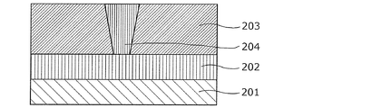
- a first contact plug is formed between the substrate and the first electrode, and the first contact plug has a side surface covered with a second insulating film.
- the upper surface of the first contact plug is formed so as to project from the upper surface of the second insulating film, and the first electrode is formed of the upper surface of the first contact plug and the second insulating film around the upper surface.
- a second step may be formed so as to extend over the upper surface, and the first step may be a step obtained by transferring the second step to the upper surface of the metal oxide layer.
- the first step may have a downward convex shape.
- a first contact plug is formed between the substrate and the first electrode, and the first contact plug has a second insulating film around the side surface thereof. It is covered, and the upper surface of the first contact plug is formed by being recessed from the upper surface of the second insulating film, and the first electrode is the upper surface of the first contact plug and the second insulating film around the upper surface.
- a third step formed over the upper surface of the metal oxide layer, and the first step may be a step formed by transferring the third step to the upper surface of the metal oxide layer.
- the second electrode may include a material having a catalytic action to dissociate the hydrogen atom from the gas molecule.
- the second electrode may include platinum or palladium.
- the metal oxide layer reversibly has a high resistance state and a low resistance state based on a voltage applied between the first electrode and the second electrode. You may transit between and.
- a current detection unit that detects a current flowing through the metal oxide layer when a predetermined voltage is applied between the first electrode and the second electrode is provided. Further, the decrease of the resistance value may be detected by the increase of the current detected by the current detection unit.
- the metal oxide layer may include a transition metal oxide.
- the transition metal oxide may be any of tantalum oxide, hafnium oxide, and zirconium oxide.
- the second contact plug connected to the second electrode through a part of the portion of the first insulating film covering the second electrode and the said. And a conductor connected to the second contact plug above the second contact plug.
- the method for manufacturing a gas sensor includes a step of forming a first electrode film on a substrate and a metal oxide film having a first step on the upper surface on the first electrode film. And a step of forming a second electrode film on the metal oxide film, and the first electrode film, the metal oxide film, and the second electrode film so as to include the first step in a plan view.
- the method for manufacturing a gas sensor includes a step of forming a second insulating film on the substrate, a step of forming a first contact plug in the second insulating film, and the first step.
- the step of removing the upper portion of the second insulating film around the contact plug and projecting the upper surface of the first contact plug from the upper surface of the surrounding second insulating film further includes the step of projecting the upper surface of the first contact plug.
- the first electrode film and the metal oxidation are sequentially formed on the first contact plug and the second insulating film so as to straddle the second step which is a step between the upper surface and the upper surface of the second insulating film around the upper surface.
- the material film and the second electrode film may be formed, and the gas detection element having the first step to which the second step is transferred may be formed.
- the method for manufacturing a gas sensor includes a step of forming a second insulating film on the substrate, a step of forming a first contact plug in the second insulating film, and the above.
- the step of removing the upper portion of the first contact plug and denting the upper surface of the first contact plug from the upper surface of the surrounding second insulating film further includes the step of removing the upper surface of the first contact plug and the surrounding surface thereof.
- the first electrode film, the metal oxide film, and the second film are sequentially formed on the first contact plug and the second insulating film so as to extend over a third step that is a step with the upper surface of the second insulating film.
- An electrode film may be formed to form the gas detection element having the first step to which the third step is transferred.
- the fuel cell vehicle includes a passenger compartment, a gas tank chamber in which a hydrogen gas tank is arranged, a fuel cell chamber in which a fuel cell is arranged, and a gas sensor according to any one of the above.
- the gas sensor is disposed in at least one of the gas tank chamber and the fuel cell chamber.
- the gas sensor according to the first embodiment is a gas sensor having a metal-insulating film-metal (MIM) structure in which a metal oxide layer as an insulating film and a metal film are stacked.
- the gas sensor can detect hydrogen-containing gas without heating with a heater by utilizing self-heating and gas sensitivity in a local region formed in the metal oxide layer.
- the hydrogen-containing gas is a general term for gases composed of molecules having hydrogen atoms, and may include hydrogen, methane, alcohol, and the like, as an example.
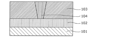
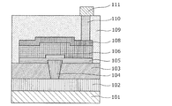
- FIG. 1A is a cross-sectional view showing a configuration example of the gas sensor 100 according to the present embodiment.
- FIG. 1B is a top view showing a configuration example of the gas sensor 100 according to the present embodiment.
- FIG. 1A corresponds to the cross section seen in the direction of the arrow in the cutting line of IA-IA'in FIG. 1B.
- the gas sensor 100 is connected to the first wiring 102 through the substrate 101, the first wiring 102, the second insulating film 103 arranged on the first wiring 102, and the second insulating film 103.
- a first insulating film 109 that covers at least a part of the oxide layer 106 and the second electrode 108, a second contact plug 110 that penetrates the first insulating film 109 and is connected to the second electrode 108, and a second contact plug.
- the second wiring 111 is formed on the first insulating film 109 so as to be connected to the first insulating film 109.
- the upper surface of the first contact plug 104 is formed at a position higher than the upper surface of the second insulating film 103, and the second step 122 is formed by the first contact plug 104 and the second insulating film 103 adjacent thereto. ing.
- the first electrode 105, the metal oxide layer 106, and the second electrode 108 are transferred so as to transfer the second step 122 formed by the first contact plug 104 and the second insulating film 103 adjacent thereto.
- a first step 121 is formed above the 1 contact plug 104.
- the first insulating film 109 has an opening 109 a formed on the second electrode 108 to expose the upper surface of the second electrode 108.
- the first step of the second electrode 108 that transfers the second step 122 formed by the first contact plug 104 and the second insulating film 103 adjacent thereto is on the bottom surface of the opening 109a. 121 is exposed.
- the first step 121 has an upward convex shape. It is not essential that the first step 121 is exposed on the upper surface of the second electrode 108, and the first step 121 has an opening 109a at the interface between the metal oxide layer 106 and the second electrode 108 in a plan view. It suffices if it is formed in a portion located inside.
- the metal oxide layer 106 is a layer whose resistance value reversibly changes based on an electric signal applied between the first electrode 105 and the second electrode 108.
- the metal oxide layer 106 is in a high resistance state depending on the voltage applied between the first electrode 105 and the second electrode 108 and the presence or absence of a hydrogen-containing gas in the gas with which the second electrode 108 is in contact. It makes a reversible transition to and from the low resistance state.
- the metal oxide layer 106 there is a local region 107 that is in contact with the second electrode 108 but not in contact with the first electrode 105.
- the local region 107 is a minute region including a filament composed of oxygen defect sites, and the filament functions as a conductive path.
- the metal oxide layer 106 is composed of a metal oxide, and the oxygen deficiency of the metal oxide contained in the local region 107 of the metal oxide layer 106 depends on the local region of the metal oxide layer 106. It is larger than the oxygen deficiency of the metal oxide contained in the portion other than 107.
- the oxygen deficiency of the metal oxide contained in the local region 107 depends on the voltage applied between the first electrode 105 and the second electrode 108 and the hydrogen content in the gas with which the second electrode 108 contacts through the opening 109a. It reversibly changes depending on the presence or absence of gas.
- the “oxygen deficiency” means the ratio of oxygen deficient to the amount of oxygen contained in the oxide of the stoichiometric composition in the metal oxide.
- the stoichiometric composition of the metal oxide in the present specification is a plurality of stoichiometric compositions. It means a stoichiometric composition with the highest resistance value in the composition.
- the metal oxide in the stoichiometric composition is more stable and has a higher resistance value than the metal oxides in the other stoichiometric composition states.
- the oxide of stoichiometric composition as defined above is Ta 2 O 5 .
- Ta 2 O 5 can also be expressed as Ta O 2.5 .
- the oxygen deficiency of TaO 2.5 is 0%.
- a metal oxide having a low oxygen deficiency is closer to a metal oxide having a stoichiometric composition and thus has a higher resistance value, and a metal oxide having a high oxygen deficiency is closer to a metal that is a component of the metal oxide The resistance is low.
- the "oxygen content” means the ratio of oxygen atoms to the total number of atoms.
- the oxygen content of Ta 2 O 5 is the ratio of oxygen atoms to the total number of atoms (O/(Ta+O)), which is 71.4 atm %. Therefore, the oxygen content of the oxygen-deficient tantalum oxide is greater than 0 and less than 71.4 atm%.
- the local region 107 is formed in the metal oxide layer 106 by applying an initial break voltage between the first electrode 105 and the second electrode 108.
- the initial break voltage is more absolute than a normal write voltage applied between the first electrode 105 and the second electrode 108 to reversibly transition the metal oxide layer 106 between a high resistance state and a low resistance state. It may be a voltage having a large value or a voltage having an absolute value smaller than the writing voltage. Further, the initial break voltage may be applied repeatedly or continuously for a predetermined time.
- a local region 107 that contacts the second electrode 108 but does not contact the first electrode 105 is formed in the metal oxide layer 106.
- the local region 107 is concentrated in the vicinity of the first step 121 of the metal oxide layer 106 to which the second step 122 formed between the first contact plug 104 and the second insulating film 103 is transferred. Generated.
- Local region 107 is considered to contain filaments composed of oxygen defective sites. Further, the size of the local region 107 is a minute size commensurate with the filament required for passing an electric current. The formation of filaments in the local region 107 is explained using a percolation model.
- the percolation model assumes a random distribution of oxygen defective sites (hereinafter simply referred to as defective sites) in the local region 107, and the probability that defective site connections are formed when the density of defective sites exceeds a certain threshold. Is a model based on the theory that
- the filament is composed of a plurality of defective sites connected in the local region 107. Further, according to the percolation model, the resistance change in the metal oxide layer 106 appears due to the generation and disappearance of defect sites in the local region 107.
- defect means that oxygen is missing from the stoichiometric composition in the metal oxide.
- density of defect sites corresponds to the degree of oxygen deficiency. That is, as the degree of oxygen deficiency increases, so does the density of defective sites.
- Only one local region 107 may be formed on the metal oxide layer 106 of the gas sensor 100.
- the number of local regions 107 in the metal oxide layer 106 can be confirmed by, for example, EBAC (Electron Beam Absorbed Current) analysis.
- the local region 107 By forming the local region 107 in the metal oxide layer 106, when a voltage is applied between the first electrode 105 and the second electrode 108, the current in the metal oxide layer 106 is concentrated in the local region 107. Flow to. Since the local region 107 is minute, for example, heat generation due to a current of about several tens of ⁇ A (that is, power consumption of less than 0.1 mW) when a voltage of about 1 V is applied to read the resistance value causes a considerable temperature rise. ..
- the second electrode 108 is made of a catalytic metal, for example, platinum, and the contact region of the second electrode 108 with the local region 107 is heated by the heat generated by the local region 107 to generate hydrogen atoms from the hydrogen-containing gas. Increase the efficiency of dissociation.
- the hydrogen atoms dissociated from the hydrogen-containing gas at the second electrode 108 are combined with the oxygen atoms in the local region 107, and the resistance value of the local region 107 is reduced. descend.
- the gas sensor 100 has a characteristic that the resistance value of the metal oxide layer 106 decreases when the second electrode 108 comes into contact with the hydrogen-containing gas by the above mechanism. Due to this characteristic, the gas to be inspected is brought into contact with the second electrode 108, and the resistance value between the first electrode 105 and the second electrode 108 is lowered to reduce the hydrogen-containing gas contained in the gas to be inspected. Can be detected.
- the hydrogen-containing gas comes into contact with the second electrode 108, so that the resistance value further decreases. Therefore, the hydrogen-containing gas can be detected by a gas sensor in which the local region 107 is in either a high resistance state or a low resistance state. However, in order to more clearly detect the decrease in the resistance value, a gas sensor in which the local region 107 is electrically set to a high resistance state may be used. ..
- the metal oxide layer 106 contains oxygen-deficient metal oxide.
- the base metal of the metal oxide includes transition metals such as tantalum, hafnium (Hf), titanium (Ti), zirconium (Zr), niobium (Nb), tungsten (W), nickel (Ni), and iron (Fe). , At least one may be selected from the group consisting of aluminum (Al).
- transition metals can have a plurality of oxidation states, different resistance states can be realized by a redox reaction.
- the oxygen-deficient metal oxide refers to a metal oxide having a smaller oxygen content (atomic ratio) than the composition of a metal oxide having a stoichiometric composition, which is usually an insulator. Many oxygen-deficient metal oxides usually behave like a semiconductor. By using the oxygen-deficient metal oxide for the metal oxide layer 106, it is possible to realize a highly reproducible and stable resistance change operation in the gas sensor 100.
- the resistance value of the metal oxide layer 106 is 1.6 or more when the composition is expressed as HfO x. Can be changed stably.
- the film thickness of the hafnium oxide may be 3 nm to 4 nm.
- the resistance value of the metal oxide layer 106 when x is 1.4 or more when the composition is expressed as ZrO x. Can be changed stably.
- the film thickness of the zirconium oxide may be 1 to 5 nm.
- the resistance value of the metal oxide layer 106 when x is 2.1 or more when the composition is expressed as TaO x. Can be changed stably.
- composition of each metal oxide layer shown above can be measured using the Rutherford backscattering method.
- the materials of the first electrode 105 and the second electrode 108 are, for example, platinum, iridium (Ir), palladium (Pd), silver (Ag), nickel, tungsten, copper (Cu), aluminum, tantalum, titanium, and nitride. It may be selected from titanium (TiN), tantalum nitride (TaN) and titanium aluminum nitride (TiAlN).
- the material of the second electrode 108 for example, a material having a catalytic action for dissociating a hydrogen atom from a gas molecule having a hydrogen atom such as platinum, iridium, and palladium may be used.
- a material having a lower standard electrode potential than the metal constituting the metal oxide such as tungsten, nickel, tantalum, titanium, aluminum, tantalum nitride, and titanium nitride, is used. Good.
- the higher the standard electrode potential the more difficult it is to oxidize.
- the substrate 101 for example, a silicon single crystal substrate or a semiconductor substrate can be used, but the substrate 101 is not limited thereto. Since the metal oxide layer 106 can be formed at a relatively low substrate temperature, for example, the metal oxide layer 106 can be formed on a resin material or the like.
- the gas sensor 100 may further include, for example, a fixed resistor, a transistor, or a diode as a load element electrically connected to the metal oxide layer 106.
- the gas sensor 100 may include a measurement circuit for measuring the current flowing through the metal oxide layer 106 when a predetermined voltage is applied between the first electrode 105 and the second electrode 108.
- the gas sensor 100 may include a power supply circuit that constantly applies a predetermined voltage between the first electrode 105 and the second electrode 108. According to such a configuration, a highly convenient gas sensor can be obtained as a module component including a measurement circuit or a power supply circuit.
- the wiring shape is patterned by a photolithography method, and then the aluminum is etched by a dry etching method to form the wiring shape.
- the first wiring 102 is formed by processing. At that time, for example, an insulating film formed by a CVD (Chemical Vapor Deposition) method may be sandwiched between the first wiring 102 and the silicon substrate 101. Further, the first wiring 102 may be copper in addition to aluminum, and adhesion layers such as titanium and titanium nitride may be formed above and below the aluminum.
- a silicon oxide film is deposited to a thickness of 500 nm on the first wiring 102 by, for example, a CVD method to form a second insulating film 103.
- the second insulating film 103 may have a laminated structure of a silicon oxide film and a silicon nitride film.
- a mask patterned into a hole shape is arranged on the second insulating film 103 by the photolithography method, and then the second insulating film 103 is penetrated by the dry etching method using the mask to reach the first wiring 102.
- Form holes (not shown).
- a tungsten film is formed on the entire surface of the 800 nm wafer by a CVD method, and a first contact plug film 104a is formed in the hole so as to be in contact with the first wiring 102.
- the first contact plug film 104a may be copper, or titanium, titanium nitride, tantalum, nitride may be provided between the first contact plug film 104a made of tungsten or copper and the first wiring 102 and the second insulating film 103. It is also possible to form an adhesion layer such as tantalum and a barrier layer.
- the first contact plug film 104a is polished by the CMP (Chemical Mechanical Polishing) method until the second insulating film 103 is exposed, and the first contact plug 104 is formed in the hole.
- CMP Chemical Mechanical Polishing
- the surface of the first contact plug film 104a is set to be at least as high as or lower than the surface of the surrounding second insulating film 103.
- the upper part of the second insulating film 103 is etched by, for example, 50 nm with a chemical solution containing hydrofluoric acid (HF) by a wet etching method, and the upper surface of the first contact plug 104 is subjected to the first contact plug. It is projected from the surface of the second insulating film 103 formed on the peripheral side surface of the 104. In this way, the second step 122 is formed at the boundary between the first contact plug 104 and the second insulating film 103.
- HF hydrofluoric acid
- the first electrode film 105a for example, a tantalum nitride film having a thickness of 30 nm is projected from the surfaces of the second insulating film 103 and the second insulating film 103 by a sputtering method. Is formed so as to cover the surface of. At that time, the first electrode film 105a may be a laminated film such as titanium or titanium nitride.
- a metal oxide film 106a having a thickness of 30 nm is formed on the first electrode film 105a by a reactive sputtering method using, for example, a Ta target.
- a platinum film having a thickness of 10 nm, for example, is formed as the second electrode film 108a on the metal oxide film 106a by a sputtering method.
- the thickness of the platinum film is preferably 5 nm or more and 200 nm or less.
- the first electrode film 105a, the metal oxide film 106a, and the second electrode film 108a Is transferred to the first electrode film 105a, the metal oxide film 106a, and the second electrode film 108a, and the first step 121 is formed near the boundary region between the first contact plug 104 and the second insulating film 103 in the second electrode film 108a. It becomes a structure to have.
- a first mask 112 by a photoresist is formed in a sensor shape on the second electrode film 108a including the first step 121 in a plan view, for example, by a photolithography method.
- the dimension of the first mask 112 in plan view may be, for example, about 1 ⁇ m square to 8 ⁇ m square.
- the first electrode film 105a, the metal oxide film 106a, and the second electrode film 108a are patterned into the shape of the gas detection element by dry etching using the first mask 112, and the first A gas detection element including the electrode 105, the metal oxide layer 106, and the second electrode 108 is formed.
- a silicon oxide film of, eg, 800 nm is formed as the first insulating film 109 so as to cover at least a part of the metal oxide layer 106 and the second electrode 108.
- the upper portion of the first insulating film 109 is polished to a thickness of 300 nm by the CMP method to flatten the surface of the first insulating film 109.
- a via hole is provided which penetrates the first insulating film 109 by etching and reaches a part of the second electrode 108, then a tungsten film is formed on the entire surface of an 800 nm wafer by a CVD method, and tungsten is deposited only in the plug by a CMP method.
- the second contact plug 110 is formed by flattening until it remains in the wafer. After that, a new conductor film is deposited on the first insulating film 109 and patterned to form a second wiring 111 connected to the second contact plug 110.
- a second mask 113 made of a photoresist is formed on the first insulating film 109 by a lithography method.
- the opening of the second mask 113 is formed inside the second electrode 108 and in a shape including the entire first step 121 formed in the second electrode 108.
- the first insulating film 109 is etched by a dry etching method using the second mask 113 to form an opening 109a that exposes a part of the surface of the second electrode 108.
- a local region 107 is formed in the metal oxide layer 106 by applying an initial break voltage between the first electrode 105 and the second electrode 108 in the gas sensor 100. Then, the gas sensor 100 is completed.
- the local region 107 is the first step 121 portion of the metal oxide layer 106 to which the second step 122 formed between the first contact plug 104 and the second insulating film 103 is transferred. That is, it is concentrated in the vicinity of the first step 121 formed on the second electrode 108.
- FIG. 4 is a measurement result showing an example of resistance change characteristics of the gas sensor 100 of the present embodiment due to voltage application.
- the sizes of the first electrode 105, the second electrode 108, and the metal oxide layer 106 are all 3 ⁇ m ⁇ 3 ⁇ m (area 9 ⁇ m 2 ).
- the initial break voltage (for example, 3V) is set to the first electrode 105 and the second electrode 108.
- the resistance value changes to the low resistance value LR by applying the voltage during the period (step S301).
- a writing voltage between the first electrode 105 and the second electrode 108 of the gas sensor 100 for example, two types of voltage pulses having a pulse width of 100 ns and different polarities, that is, a positive voltage pulse (for example, 2.5 V).
- a negative voltage pulse for example, 1.8 V
- the resistance value of the metal oxide layer 106 changes as shown in FIG.
- the resistance value of the metal oxide layer 106 increases from the low resistance value LR to the high resistance value HR (step S302).
- a negative voltage pulse is applied as a write voltage between the electrodes, the resistance value of the metal oxide layer 106 decreases from the high resistance value HR to the low resistance value LR (step S303).
- the polarity of the voltage pulse is “positive” when the potential of the second electrode 108 is high with respect to the potential of the first electrode 105, and the potential of the second electrode 108 is low with respect to the potential of the first electrode 105. The case is defined as "negative".
- a positive voltage pulse is finally applied between the first electrode 105 and the second electrode 108 before starting the monitoring of the hydrogen-containing gas.
- the gas sensor 100 is set in a high resistance state.
- the initial setting is made in this way, the decrease in the resistance value can be detected more clearly as compared with the case where the hydrogen-containing gas is detected by using the gas sensor 100 in the low resistance state as described above. Detection characteristics are improved.
- FIG. 5 is a graph showing an evaluation example of the gas sensor 100 of this embodiment.
- the horizontal axis represents time (au), and the vertical axis represents the current value (au) flowing between the first electrode 105 and the second electrode 108.
- nitrogen gas was first introduced into a closed container in which the gas sensor 100 was placed, then the nitrogen gas was switched to hydrogen gas, and then the hydrogen gas was further switched to nitrogen gas. Further, the gas sensor 100 in which the local region 107 is set to a high resistance state by applying a predetermined voltage in advance between the first electrode 105 and the second electrode 108 was used.
- FIG. 5 shows the evaluation results at this time, and the horizontal axis shows the three periods in which the first nitrogen introduction (step S501), the hydrogen introduction (step S502), and the subsequent nitrogen introduction (step S503) were performed. .. It can be seen that the current value begins to increase immediately after switching the introduction gas from nitrogen gas to hydrogen gas. In addition, it can be seen that the current begins to decrease immediately after switching the introduction gas from hydrogen gas to nitrogen gas.
- the hydrogen-containing gas monitoring operation when a detection voltage of 0.6 V is applied between the first electrode 105 and the second electrode 108, the first electrode 105 is in a state where hydrogen gas is detected. A current of 10 ⁇ A to 20 ⁇ A flowed between the second electrode 108 and the second electrode 108. That is, according to the gas sensor 100 of the present embodiment, it can be seen that the hydrogen-containing gas can be monitored with a very small power consumption of 0.006 mW to 0.012 mW.
- the inventors infer the hydrogen gas detection mechanism of the gas sensor 100 as follows.
- this hydrogen atom causes a reduction reaction of the metal oxide in the local region 107, and the oxygen in the local region 107 is combined with hydrogen to reduce the oxygen deficiency of the metal oxide contained in the local region 107.
- the filaments in the local region 107 are easily connected, and the resistance value of the local region 107 is reduced.
- the current flowing between the first electrode 105 and the second electrode 108 increases.
- the operation described above is not limited to the gas sensor 100 of the present embodiment, and it is considered that the gas sensor 100 of the present embodiment has substantially the same structure as the gas sensor 100 of the present embodiment and other gas sensors described later. ..
- the above-described operation is not limited to the case where the gas contacting the second electrode 108 is hydrogen gas, and it is considered that the same occurs when the gas is a hydrogen-containing gas such as methane or alcohol.
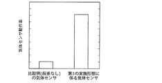
- FIG. 6 shows a gas sensor according to a comparative example (hereinafter referred to as a gas sensor having no step) formed by the same method as the gas sensor according to the present embodiment except that no step is formed and the gas sensor according to the present embodiment. It is a result of comparing the initial break voltage of the metal oxide layer 106 for the gas sensor.
- the gas sensor of this embodiment has a lower initial break voltage. This is because the step shape formed on the first contact plug 104 and the second insulating film 103 is also transferred to the first electrode 105, the metal oxide layer 106, and the second electrode 108, so that the electric field concentration is concentrated at the step portion. This is because the effective voltage applied to the metal oxide layer 106 increases due to the generation. Therefore, the local region 107 is selectively formed near the step portion.
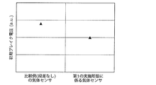
- FIG. 7 shows operation rates of the gas sensor having no step and the gas sensor formed in the present embodiment when the hydrogen concentration in the gas to be detected is set to 1%, for example.
- the operating rate of the gas sensor formed in the present embodiment is improved as compared with the operating rate of the gas sensor without steps.
- the gas sensor having no step has no step inside the sensor, and therefore the local region 107 is formed at random, and thus may be formed at a portion covered with the first insulating film 109, for example.
- hydrogen may not reach the local region 107, and does not operate as a gas sensor.
- the local region 107 is highly likely to be selectively formed at the stepped portion near the first contact plug 104, and the opening 109a is always formed in the first contact plug 104. Since it is formed so as to include immediately above, hydrogen can reach the local region 107 through the second electrode 108, so that the operating rate as a gas sensor is improved.
- the gas sensor 100 it is possible to stably detect the hydrogen-containing gas without the need to separately heat it with a heater, and thus a gas sensor excellent in power saving can be obtained.
- the gas sensor according to the second embodiment is a metal-insulation film-metal (MIM) formed by laminating a metal oxide layer as an insulation film and a metal film, like the gas sensor of the first embodiment described above. It is a gas sensor with a structure.
- the gas sensor can detect hydrogen-containing gas without heating with a heater by utilizing self-heating and gas sensitivity in a local region formed in a gas-sensitive resistance film.
- the hydrogen-containing gas is a general term for gases composed of molecules having hydrogen atoms, and may include hydrogen, methane, alcohol, and the like, as an example.
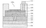
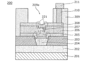
- FIG. 8A is a cross-sectional view showing a configuration example of the gas sensor 200 according to the present embodiment.
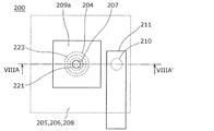
- FIG. 8B is a top view showing a configuration example of the gas sensor 200 according to the present embodiment.
- FIG. 8A corresponds to the cross section viewed in the direction of the arrow in the cutting line of VIIIA-VIIIA'of FIG. 8B.
- the gas sensor 200 includes a substrate 201, a first wiring 202, a second insulating film 203 disposed on the first wiring 202, and a first wiring 202 penetrating the second insulating film 203 and connected to the first wiring 202.
- the upper surface of the first contact plug 204 is formed at a position lower than the upper surface of the second insulating film 203, and the third step 223 is formed by the first contact plug 204 and the second insulating film 203 adjacent thereto. ing.
- the first contact 205, the metal oxide layer 206, and the second electrode 208 are formed so that the third step 223 formed of the first contact plug 204 and the second insulating film 203 adjacent thereto is transferred.
- a first step 221 is formed above the one contact plug 204.
- the first insulating film 209 has an opening 209 a formed on the second electrode 208 to expose the upper surface of the second electrode 208.
- the first step of the second electrode 208 that transfers the third step 223 formed by the first contact plug 204 and the second insulating film 203 adjacent thereto on the bottom surface of the opening 209a. 221 is exposed.
- the first step 221 has a downward convex shape. It is not essential that the first step 221 is exposed on the upper surface of the second electrode 208, and the first step 221 has an opening 209a in a plan view of the interface between the metal oxide layer 206 and the second electrode 208. It suffices if it is formed in the portion located inside.
- the metal oxide layer 206 is a layer whose resistance value reversibly changes based on an electric signal applied between the first electrode 205 and the second electrode 208.
- the metal oxide layer 206 is in a high resistance state depending on the voltage applied between the first electrode 205 and the second electrode 208 and the presence or absence of a hydrogen-containing gas in the gas with which the second electrode 208 is in contact. It makes a reversible transition to and from the low resistance state.
- the metal oxide layer 206 there is a local region 207 that is in contact with the second electrode 208 but is not in contact with the first electrode 205.
- the local region 207 is a minute region containing a filament composed of oxygen-deficient sites, and the filament functions as a conductive path.
- the metal oxide layer 206 is composed of a metal oxide, and the oxygen deficiency of the metal oxide contained in the local region 207 of the metal oxide layer 206 is determined by the local region of the metal oxide layer 206. It is higher than the oxygen deficiency of the metal oxide contained in the portion other than 207.
- the oxygen deficiency of the metal oxide contained in the local region 207 depends on the voltage applied between the first electrode 205 and the second electrode 208 and the hydrogen content in the gas with which the second electrode 208 contacts through the opening 209a. It reversibly changes depending on the presence or absence of gas.
- the gas sensor 200 configured as described above has the following effects.
- a local region 207 that is in contact with the second electrode 208 but is not in contact with the first electrode 205 is formed in the metal oxide layer 206.
- the local region 207 is formed in the first portion of the metal oxide layer 206 to which the third step 223 formed between the first contact plug 204 and the second insulating film 203 is transferred. It is generated concentratedly in the vicinity of the first step 221.
- the mechanism of the resistance change phenomenon and the hydrogen detection in the gas sensor 200 is the same as the mechanism of the resistance change phenomenon and the hydrogen detection in the gas sensor 100 of the first embodiment, and thus the repeated description thereof will be omitted.
- the wiring shape is formed.
- the first wiring 202 is formed by processing. At that time, an insulating film may be sandwiched between the first wiring 202 and the silicon substrate 201, for example, by a CVD method. Further, the first wiring 202 may be copper instead of aluminum, and an adhesion layer of titanium, titanium nitride, or the like may be formed above and below aluminum.
- a silicon oxide film is deposited to a thickness of 500 nm on the first wiring 202 by, for example, a CVD method to form a second insulating film 203.
- the second insulating film 203 may have a laminated structure of a silicon oxide film and a silicon nitride film.
- a mask patterned into a hole shape is arranged on the second insulating film 203 by the photolithography method, and then the second insulating film 203 is penetrated by the dry etching method using the mask to reach the first wiring 202.
- Form holes (not shown).
- tungsten is formed on the entire surface of the 800 nm wafer by the CVD method, and the first contact plug film 204a is formed in the hole so as to be in contact with the first wiring 202.
- the first contact plug film 204a may be copper, or titanium, titanium nitride, tantalum, nitride may be provided between the first contact plug film 204a made of tungsten, copper, etc. and the first wiring 202 and the second insulating film 203. It is also possible to form an adhesion layer such as tantalum and a barrier layer.
- the first contact plug film 204a is polished by CMP until the second insulating film 203 is exposed to form the first contact plug 204 in the hole.
- the surface of the first contact plug film 204a is set to be at least as high as or lower than the surface of the surrounding second insulating film 203.
- W is etched by, for example, 30 nm by a dry etching method, and the upper surface of the first contact plug 204 is covered with the second insulating film 203 formed on the peripheral side surface of the first contact plug 204. It is formed so as to be lower than the surface.
- the third step 223 is formed at the boundary between the first contact plug 204 and the second insulating film 203, as in the gas sensor according to the first embodiment. The difference from the first embodiment is that the third step 223 is formed without etching the large-area second insulating film 203.
- the first electrode film 205a for example, a tantalum nitride film having a thickness of 30 nm is recessed from the surfaces of the second insulating film 203 and the second insulating film 203 by a sputtering method. Is formed so as to cover the surface of. At that time, the first electrode film 205a may be a laminated film of titanium, titanium nitride, or the like.
- a metal oxide film 206a having a thickness of 30 nm is formed on the first electrode film 205a by a reactive sputtering method using a tantalum target, for example.
- a platinum film having a thickness of 10 nm, for example, is formed as the second electrode film 208a on the metal oxide film 206a by a sputtering method.
- the thickness of the platinum film is preferably 5 nm or more and 200 nm or less.
- the third step 223 between the surface of the first contact plug 204 and the surface of the second insulating film 203 formed so as to be recessed below the surface of the surrounding second insulating film 203 is formed.
- a first mask 212 made of photoresist is formed in a sensor shape on the second electrode film 208a including the first step 221 in a plan view by, for example, photolithography.
- the dimensions of the first mask 212 may be, for example, about 1 ⁇ m square to 8 ⁇ m square.
- the first electrode film 205a, the metal oxide film 206a, and the second electrode film 208a are patterned into the shape of the gas detection element by dry etching using the first mask 212, and the first A gas sensing element including the electrode 205, the metal oxide layer 206, and the second electrode 208 is formed.
- the first insulating film 209 for example, an 800 nm silicon oxide film is formed so as to cover at least a part of the metal oxide layer 206 and the second electrode 208.
- the upper portion of the first insulating film 209 is polished by 300 nm by the CMP method to flatten the surface of the first insulating film 209.
- tungsten is formed on the entire surface of the 800 nm wafer by the CVD method, and the tungsten is formed only in the plug by the CMP method.
- the second contact plug 210 is formed by flattening until it remains. Then, a new conductor film is deposited on the first insulating film 209 and patterned to form the second wiring 211 connected to the second contact plug 210.
- a second mask 213 made of photoresist is formed on the first insulating film 209 by a lithography method.
- the opening of the second mask 213 is formed inside the second electrode 208 and in a shape including the entire first step 221 formed on the second electrode 208.
- the first insulating film 209 is etched by a dry etching method using the second mask 213 to form an opening 209a that exposes a part of the surface of the second electrode 208.
- an initial break voltage is applied between the first electrode 205 and the second electrode 208 in the gas sensor 200 to form a local region 207 in the metal oxide layer 206.
- the gas sensor 200 is completed.
- the local region 207 is the first step 221 portion of the metal oxide layer 206 to which the third step 223 formed between the first contact plug 204 and the second insulating film 203 is transferred. That is, it is concentrated in the vicinity of the first step 221 formed on the second electrode 108.
- the resistance change characteristic of the gas sensor 200 configured as described above due to voltage application is equivalent to the resistance change characteristic of the gas sensor 100 described with reference to FIGS. 4 and 5.
- the resistance change due to the hydrogen-containing gas of the gas sensor 200 occurs by the same mechanism as the mechanism described for the gas sensor 100.
- the gas sensor 200 it is not necessary to separately heat the gas with a heater, and hydrogen-containing gas can be stably detected, so that a gas sensor having excellent power saving can be obtained.
- the fuel cell vehicle according to the third embodiment includes any of the gas sensors described in the first and second embodiments described above and their modifications, and the gas sensor detects hydrogen gas in the vehicle. ..
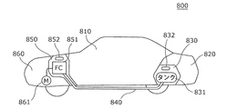
- FIG. 11 is a side view showing a configuration example of the fuel cell vehicle 800 according to the third embodiment.
- the fuel cell vehicle 800 includes a passenger compartment 810, a luggage compartment 820, a gas tank compartment 830, a fuel tank 831, a gas sensor 832, a pipe 840, a fuel cell compartment 850, a fuel cell 851, a gas sensor 852, a motor compartment 860, and a motor 861.
- the fuel tank 831 is provided in the gas tank chamber 830 and holds hydrogen gas as the fuel gas.
- the gas sensor 832 detects a fuel gas leak in the gas tank chamber 830.
- the fuel cell 851 includes a fuel cell stack in which a plurality of cells, which are basic units having a fuel electrode, an air electrode, and an electrolyte, are stacked.
- the fuel cell 851 is provided in the fuel cell chamber 850.
- the hydrogen gas in the fuel tank 831 is sent to the fuel cell 851 in the fuel cell chamber 850 through the pipe 840. Electric power is generated by reacting this hydrogen gas with oxygen gas in the atmosphere in the fuel cell 851.
- the gas sensor 852 detects hydrogen gas leakage in the fuel cell chamber 850.
- the motor 861 is provided in the motor chamber 860.
- the motor 861 is rotated by the electric power generated by the fuel cell 851 to drive the fuel cell vehicle 800.
- the gas sensor according to the present disclosure can detect a hydrogen-containing gas with a very small power consumption of about 0.01 mW, for example. Therefore, by utilizing the excellent power saving property of the gas sensor, it is possible to constantly monitor the hydrogen gas leakage without significantly increasing the standby power of the fuel cell vehicle.
- a predetermined voltage is constantly applied to the gas sensors 832 and 852, and the fuel tank in the gas tank chamber 830 is based on the amount of current flowing through the gas sensors 832 and 852. It may be determined whether or not hydrogen gas exists outside the fuel cell 851 in the fuel cell chamber 850 and outside the fuel cell chamber 850.
- the gas sensor is driven to determine the presence or absence of hydrogen gas leakage after the ignition key is operated.
- the starting time of the fuel cell vehicle can be shortened.
- safety can be improved by continuing to monitor the hydrogen gas leakage even after the fuel cell vehicle is running, for example, after the fuel cell vehicle is stored in the garage.
- the present embodiment includes various modifications that can be conceived by those skilled in the art, and a form constructed by combining the components of each embodiment within the scope of the present disclosure. is there.
- the gas sensor described above may further include a measuring circuit for measuring the current flowing through the metal oxide layer when a predetermined voltage is applied between the first electrode and the second electrode.
- the gas sensor described above may further include a power supply circuit that constantly applies a predetermined voltage between the first electrode and the second electrode.
- a highly convenient gas sensor can be obtained as a module component provided with a measurement circuit or a power supply circuit.
- the gas sensor according to the present disclosure functions as a gas sensor having excellent power saving properties, and is useful as a hydrogen sensor used in, for example, a fuel cell vehicle.
Abstract
A gas sensor (100) comprises: a gas detection element comprising a first electrode (105), a metal oxide layer (106), and a second electrode (108); and a first insulating film (109) that has an opening exposing one section of the second electrode (108) and that covers the first electrode (105), the metal oxide layer (106), and another section of the second electrode (108). The metal oxide layer (106) has a characteristic whereby a resistance value changes as a result of the second electrode (108) being in contact with a gas molecule including hydrogen atoms. A first step (121) is formed in a section positioned inside an opening (109a) in the planar view of a boundary surface between the metal oxide layer (106) and the second electrode (108). A local area (107) is formed in the vicinity of the first step (121) in the metal oxide layer (106). The oxygen deficiency in the local area (107) is greater than the oxygen deficiency in other areas in the metal oxide layer (106).
Description
本開示は、気体センサおよびその製造方法と当該気体センサを搭載した燃料電池自動車に関する。
The present disclosure relates to a gas sensor, a manufacturing method thereof, and a fuel cell vehicle equipped with the gas sensor.
近年、水素社会の実現にむけた取組みが様々な分野で精力的に行われている。特に、究極のエコカーと期待されている水素を燃料として用いる燃料電池自動車も市場に投入され、それに伴い水素ステーションなどのインフラも着実に整備されている。このような状況のなかで、水素社会の安全安心を担保するものとして、水素を検知するセンサの重要性が増してきている。
In recent years, efforts toward the realization of a hydrogen-based society have been energetically carried out in various fields. In particular, fuel cell vehicles that use hydrogen as a fuel, which is expected to be the ultimate eco-car, have been introduced to the market, and along with that, infrastructure such as hydrogen stations has been steadily developed. Under such circumstances, the importance of sensors that detect hydrogen is increasing as a way of ensuring the safety and security of a hydrogen society.
水素を代表とする気体を検知するセンサとして、気体感応性絶縁膜(以下では、単に絶縁膜とも言う)と金属膜が積層された金属-絶縁膜-金属(MIM)構造の気体検知素子を備えた気体センサが知られている。
As a sensor for detecting a gas typified by hydrogen, a gas detection element having a metal-insulating film-metal (MIM) structure in which a gas-sensitive insulating film (hereinafter, also simply referred to as an insulating film) and a metal film are laminated is provided. Gas sensors are known.
このような気体センサは、気体に少量含まれる水素、アルコール、炭化水素、アンモニア、アミンなどの検出に使用することができ、特に、水素のような反応性の高い気体を効率よく検出することができる。
Such a gas sensor can be used for detecting a small amount of hydrogen, alcohol, hydrocarbon, ammonia, amine, etc. contained in the gas, and in particular, it can efficiently detect a highly reactive gas such as hydrogen. it can.
特許文献1には絶縁膜と金属膜が積層されてなるMIM構造の気体センサが開示されている。特許文献1の気体センサは、五酸化タンタル(Ta2O5)にパラジウムとガラスを所定量添加した絶縁膜を用い、当該絶縁膜を挟み込む上下の金属電極として、白金(Pt)を用いている。
Patent Document 1 discloses a gas sensor having a MIM structure in which an insulating film and a metal film are laminated. The gas sensor of Patent Document 1 uses an insulating film in which a predetermined amount of palladium and glass are added to tantalum pentoxide (Ta 2 O 5 ), and platinum (Pt) is used as upper and lower metal electrodes sandwiching the insulating film. ..
しかしながら、従来の気体検知素子では、例えば水素原子を有する気体を検知する感度の向上のために気体検出素子を100℃以上に加熱しており、消費電力は最小のものでも100mW程度必要である。従って、気体検知素子を常時ON状態で使用する場合、消費電力が非常に大きくなるという課題がある。
However, in the conventional gas detection element, for example, the gas detection element is heated to 100 ° C. or higher in order to improve the sensitivity for detecting a gas having a hydrogen atom, and the minimum power consumption is about 100 mW. Therefore, when the gas detection element is used in the always ON state, there is a problem that the power consumption becomes very large.
本開示は、水素原子を有する気体分子を感度良く安定に検出することが可能であり、かつ、消費電力が小さい気体センサ、その製造方法および燃料電池自動車を提供する。
The present disclosure provides a gas sensor that can detect a gas molecule having a hydrogen atom with high sensitivity and stability and consumes less power, a manufacturing method thereof, and a fuel cell vehicle.
従来の課題を解決するために、本開示の一態様に係る気体センサは、第1電極、前記第1電極上に形成された金属酸化物層および前記金属酸化物層上に形成された第2電極を有し、気体中に存在しかつ水素原子を含む気体分子を検知する気体検知素子と、前記第2電極の一部を露出した開口を有し、前記第1電極、前記金属酸化物層および前記第2電極の他の一部を被覆する第1絶縁膜と、を備え、前記金属酸化物層は前記第2電極が前記気体分子に接触することでその抵抗値が変化する特性を備えており、前記金属酸化物層と前記第2電極との界面の、平面視において前記開口内に位置する部分には第1段差が形成されており、前記金属酸化物層における前記第1段差の近傍に局所領域が形成されており、前記局所領域における酸素不足度は、前記金属酸化物層における前記局所領域以外の領域の酸素不足度よりも大きい。
In order to solve the conventional problems, the gas sensor according to one aspect of the present disclosure includes a first electrode, a metal oxide layer formed on the first electrode, and a second metal oxide layer formed on the metal oxide layer. It has an electrode, a gas detection element that detects gas molecules that are present in the gas and contains hydrogen atoms, and an opening that exposes a part of the second electrode, and the first electrode and the metal oxide layer. And a first insulating film that covers another part of the second electrode, and the metal oxide layer has a property that the resistance value changes when the second electrode comes into contact with the gas molecule. A first step is formed in a portion of the interface between the metal oxide layer and the second electrode located in the opening in plan view, and the first step in the metal oxide layer is formed. A local region is formed in the vicinity, and the oxygen deficiency in the local region is higher than the oxygen deficiency in regions other than the local region in the metal oxide layer.
また、本開示の一態様に係る気体センサの製造方法は、基板上に第1電極膜を形成する工程と、前記第1電極膜上に、上面に第1段差を有する金属酸化物膜を形成する工程と、前記金属酸化物膜上に第2電極膜を形成する工程と、平面視において前記第1段差を含むように前記第1電極膜、前記金属酸化物膜および前記第2電極膜をパターニングして、第1電極、金属酸化物層および第2電極からなる気体検知素子を形成する工程と、前記気体検知素子を被覆するように第1絶縁膜を形成する工程と、前記第1絶縁膜の一部を除去して、平面視において前記第1段差上の前記第2電極の一部を露出した開口を形成する工程と、を含む。
Further, the method for manufacturing a gas sensor according to one aspect of the present disclosure includes a step of forming a first electrode film on a substrate and a metal oxide film having a first step on the upper surface on the first electrode film. And a step of forming a second electrode film on the metal oxide film, and the first electrode film, the metal oxide film, and the second electrode film so as to include the first step in a plan view. Patterning to form a gas sensing element composed of a first electrode, a metal oxide layer and a second electrode; a step of forming a first insulating film to cover the gas sensing element; The step includes removing a part of the film to form an opening in which a part of the second electrode on the first step is exposed in a plan view.
また、本開示の一態様に係る燃料電池自動車は、客室と、水素ガスのタンクが配置されたガスタンク室と、燃料電池が配置された燃料電池室と、上記気体センサと、を備え、前記気体センサが、前記ガスタンク室および前記燃料電池室のうちの少なくとも一方に配置されている。
Further, the fuel cell vehicle according to one aspect of the present disclosure includes a passenger compartment, a gas tank chamber in which a hydrogen gas tank is arranged, a fuel cell chamber in which a fuel cell is arranged, and the gas sensor. A sensor is arranged in at least one of the gas tank chamber and the fuel cell chamber.
本開示によれば、消費電力が小さく、かつ、感度良く安定に水素原子を含む気体分子を検出することが可能な気体センサ、その製造方法および燃料電池自動車を提供することができる。
According to the present disclosure, it is possible to provide a gas sensor that consumes less power and that can detect gas molecules containing hydrogen atoms with high sensitivity and stability, a method for manufacturing the same, and a fuel cell vehicle.
(本開示の基礎となった知見)
本発明者らが鋭意検討を行なった結果、従来の気体センサにおいて、以下のような問題があることを見出した。 (Findings that form the basis of this disclosure)
As a result of diligent studies by the present inventors, it has been found that the conventional gas sensor has the following problems.
本発明者らが鋭意検討を行なった結果、従来の気体センサにおいて、以下のような問題があることを見出した。 (Findings that form the basis of this disclosure)
As a result of diligent studies by the present inventors, it has been found that the conventional gas sensor has the following problems.
特許文献1に開示された気体センサでは水素を含む可燃性ガスを検知することができると記載されてはいるが、詳細なメカニズムに関する記述はない。そこで、MIS(金属-絶縁膜-半導体)構造を用いた気体センサ(Pt-Ta2O5-Si)に関する非特許文献1において開示されているメカニズムと同様の現象が特許文献1においても引き起こされていると仮定すると、そのメカニズムは以下のように説明することができる。
It is described that the gas sensor disclosed in Patent Document 1 can detect a combustible gas containing hydrogen, but there is no description regarding a detailed mechanism. Therefore, a phenomenon similar to the mechanism disclosed in Non-Patent Document 1 regarding a gas sensor (Pt—Ta 2 O 5 —Si) using a MIS (metal-insulating film-semiconductor) structure is also caused in Patent Document 1. Assuming that, the mechanism can be explained as follows.
まず、触媒作用を有する金属である白金の表面に、例えば、水素ガスを含む気体が接触した場合、白金の触媒作用により水素ガスが水素原子に分解され、その水素原子が下記の化学反応式に従って、絶縁膜中の五酸化タンタルから酸素原子を奪うことにより、五酸化タンタル中に酸素欠陥が形成され、電流が流れやすくなると考えられる。
First, when a gas containing hydrogen gas comes into contact with the surface of platinum, which is a metal having a catalytic action, the hydrogen gas is decomposed into hydrogen atoms by the catalytic action of platinum, and the hydrogen atoms are decomposed into hydrogen atoms according to the following chemical reaction formula. It is considered that by depriving the tantalum pentoxide in the insulating film of oxygen atoms, oxygen defects are formed in the tantalum pentoxide, and the current easily flows.
Ta2O5+2XH→XH2O+Ta2O5-X
Ta 2 O 5 + 2 X H → X H 2 O + Ta 2 O 5-X
一方、水素ガスを含む気体が白金の表面からなくなると、下記に示す化学反応式に従う逆プロセスが起こることで、五酸化タンタル中の酸素欠陥がなくなり、電流が流れにくくなると考えられる。
On the other hand, when the gas containing hydrogen gas disappears from the surface of platinum, the reverse process according to the chemical reaction formula shown below occurs, which eliminates oxygen defects in tantalum pentoxide and makes it difficult for current to flow.
XH2O+Ta2O5-X→Ta2O5+2XH
X H 2 O + Ta 2 O 5-X → Ta 2 O 5 + 2 X H
このようなメカニズムによって、五酸化タンタルにパラジウムとガラスを所定量添加した絶縁膜を用い、当該絶縁膜を挟み込む上下の金属電極として白金を用いたMIM構造は、水素原子を有する気体を検知する気体センサとして機能していると考えられる。
By such a mechanism, the MIM structure using an insulating film in which a predetermined amount of palladium and glass are added to tantalum pentoxide and platinum as the upper and lower metal electrodes sandwiching the insulating film is a gas that detects a gas having a hydrogen atom. It is considered to function as a sensor.
また、特許文献1に記載されているMIM構造の気体センサでは、気体検知素子に隣接して加熱ヒータが設けられている。測定時は加熱ヒータに所定の電圧を印加して、気体検知素子温度を400℃まで上昇させている。これは気体検知素子の検出感度を上げるためと考えられる。即ち、触媒作用を有する金属である白金によって水素原子を解離させているが、触媒作用により水素原子を有する分子から水素原子を解離させる割合は温度上昇に比例するため、気体検知素子温度が上昇するに従って検出感度は上がると考えられる。
In addition, in the gas sensor having the MIM structure described in Patent Document 1, a heater is provided adjacent to the gas detection element. At the time of measurement, a predetermined voltage is applied to the heater to raise the temperature of the gas detection element to 400 ° C. This is considered to increase the detection sensitivity of the gas detection element. That is, hydrogen atoms are dissociated by platinum, which is a metal having a catalytic action, but the rate at which hydrogen atoms are dissociated from molecules having a hydrogen atom by a catalytic action is proportional to the temperature rise, so the temperature of the gas detection element rises. It is considered that the detection sensitivity increases accordingly.
MIM構造の気体センサだけでなく、金属の触媒作用を利用するMIS構造の気体センサにおいても、気体検知素子に隣接して加熱ヒータが設置されており、通常、周囲温度を100℃以上に保持して使用されている。例えば、MIS構造をダイオードとして用いた前出の非特許文献1に開示された気体センサでは検出のために100℃以上の温度が必要であり、MIS構造をトランジスタとして用いた非特許文献2に開示された気体センサでは周囲温度115℃で動作させている。
Not only in the gas sensor with the MIM structure, but also in the gas sensor with the MIS structure that utilizes the catalytic action of metal, a heater is installed adjacent to the gas detection element, and the ambient temperature is usually maintained at 100 ° C. or higher. Is being used. For example, the gas sensor disclosed in the above-mentioned Non-Patent Document 1 using the MIS structure as a diode requires a temperature of 100 ° C. or higher for detection, and is disclosed in Non-Patent Document 2 using the MIS structure as a transistor. The operated gas sensor is operated at an ambient temperature of 115°C.
また、金属の触媒作用を利用した気体センサとして、非特許文献3に開示された接触燃焼式の気体センサもあるが、この接触燃焼式においても動作時は気体検知素子を200℃~300℃まで加熱している。
Further, as a gas sensor utilizing the catalytic action of a metal, there is also a contact combustion type gas sensor disclosed in Non-Patent Document 3, but even in this contact combustion type, the gas detection element is operated from 200 ° C. to 300 ° C. during operation. It is heating.
さらには、金属の触媒作用を利用しない気体センサとして、非特許文献4に開示された熱線型半導体式と気体熱伝導式の気体センサがあるが、いずれの方式においても気体検知素子は100℃以上に加熱されている。
Further, as a gas sensor that does not utilize the catalytic action of a metal, there are a heat ray type semiconductor type gas sensor and a gas heat conduction type gas sensor disclosed in Non-Patent Document 4, and in both methods, the gas detection element is 100 ° C. or higher. Is heated to.
このように、従来の気体検知素子では、水素原子を含む気体を検知する感度の向上のために気体検知素子を100℃以上に加熱しており、消費電力は最小のものでも100mW前後ある。従って、気体検知素子を常時ON状態で使用する場合、消費電力が非常に大きくなるという課題がある。
As described above, in the conventional gas detection element, the gas detection element is heated to 100 ° C. or higher in order to improve the sensitivity for detecting a gas containing a hydrogen atom, and the minimum power consumption is about 100 mW. Therefore, when the gas detection element is used in the always ON state, there is a problem that the power consumption becomes very large.
本開示の一態様に係る気体センサは、水素原子を含む気体分子を感度良く安定に検出することが可能であり、かつ、省電力性に優れる。
The gas sensor according to one aspect of the present disclosure can detect a gas molecule containing a hydrogen atom with high sensitivity and stability, and is excellent in power saving.
(本開示の態様)
本開示の一態様に係る気体センサおよび気体センサの製造方法並びに燃料電池自動車は、以下のような特徴を備える。 (Aspect of the present disclosure)
The gas sensor according to one aspect of the present disclosure, the method for manufacturing the gas sensor, and the fuel cell vehicle have the following features.
本開示の一態様に係る気体センサおよび気体センサの製造方法並びに燃料電池自動車は、以下のような特徴を備える。 (Aspect of the present disclosure)
The gas sensor according to one aspect of the present disclosure, the method for manufacturing the gas sensor, and the fuel cell vehicle have the following features.
本開示の一態様に係る気体センサは、第1電極、前記第1電極上に形成された金属酸化物層および前記金属酸化物層上に形成された第2電極を有し、気体中に存在しかつ水素原子を含む気体分子を検知する気体検知素子と、前記第2電極の一部を露出した開口を有し、前記第1電極、前記金属酸化物層および前記第2電極の他の一部を被覆する第1絶縁膜と、を備え、前記金属酸化物層は前記第2電極が前記気体分子に接触することでその抵抗値が変化する特性を備えており、前記金属酸化物層と前記第2電極との界面の、平面視において前記開口内に位置する部分には第1段差が形成されており、前記金属酸化物層における前記第1段差の近傍に局所領域が形成されており、前記局所領域における酸素不足度は、前記金属酸化物層における前記局所領域以外の領域の酸素不足度よりも大きい。
A gas sensor according to an aspect of the present disclosure has a first electrode, a metal oxide layer formed on the first electrode, and a second electrode formed on the metal oxide layer, and is present in a gas. And a gas detecting element for detecting a gas molecule containing a hydrogen atom, and an opening exposing a part of the second electrode, and another one of the first electrode, the metal oxide layer and the second electrode. A first insulating film that covers a portion of the metal oxide layer, the metal oxide layer having a characteristic that its resistance value changes when the second electrode contacts the gas molecule. A first step is formed at a portion of the interface with the second electrode located within the opening in a plan view, and a local region is formed in the vicinity of the first step in the metal oxide layer. The oxygen deficiency in the local region is higher than the oxygen deficiency in regions other than the local region in the metal oxide layer.
また、本開示の一態様に係る気体センサにおいて、前記第1段差が上凸形状であってもよい。
Further, in the gas sensor according to one aspect of the present disclosure, the first step may have an upward convex shape.
また、本開示の一態様に係る気体センサにおいて、基板と前記第1電極との間に第1コンタクトプラグが形成されており、前記第1コンタクトプラグはその側面の周囲が第2絶縁膜で覆われており、前記第1コンタクトプラグの上面は前記第2絶縁膜の上面から突出して形成されており、前記第1電極は、前記第1コンタクトプラグの上面とその周囲の前記第2絶縁膜の上面とに跨って形成された第2段差を備えており、前記第1段差は、前記金属酸化物層の上面に前記第2段差が転写された段差であってもよい。
Further, in the gas sensor according to one aspect of the present disclosure, a first contact plug is formed between the substrate and the first electrode, and the first contact plug has a side surface covered with a second insulating film. The upper surface of the first contact plug is formed so as to project from the upper surface of the second insulating film, and the first electrode is formed of the upper surface of the first contact plug and the second insulating film around the upper surface. A second step may be formed so as to extend over the upper surface, and the first step may be a step obtained by transferring the second step to the upper surface of the metal oxide layer.
また、本開示の一態様に係る気体センサにおいて、前記第1段差が下凸形状であってもよい。
Further, in the gas sensor according to one aspect of the present disclosure, the first step may have a downward convex shape.
また、本開示の一態様に係る気体センサにおいて、前記基板と前記第1電極との間に第1コンタクトプラグが形成されており、前記第1コンタクトプラグはその側面の周囲が第2絶縁膜で覆われており、前記第1コンタクトプラグの上面は前記第2絶縁膜の上面から窪んで形成されており、前記第1電極は、前記第1コンタクトプラグの上面とその周囲の前記第2絶縁膜の上面とに跨って形成された第3段差を備えており、前記第1段差は、前記金属酸化物層の上面に前記第3段差が転写された段差であってもよい。
In the gas sensor according to one aspect of the present disclosure, a first contact plug is formed between the substrate and the first electrode, and the first contact plug has a second insulating film around the side surface thereof. It is covered, and the upper surface of the first contact plug is formed by being recessed from the upper surface of the second insulating film, and the first electrode is the upper surface of the first contact plug and the second insulating film around the upper surface. A third step formed over the upper surface of the metal oxide layer, and the first step may be a step formed by transferring the third step to the upper surface of the metal oxide layer.
また、本開示の一態様に係る気体センサにおいて、前記第2電極は、前記水素原子を前記気体分子から解離させる触媒作用を有する材料を含んでもよい。
In the gas sensor according to the aspect of the present disclosure, the second electrode may include a material having a catalytic action to dissociate the hydrogen atom from the gas molecule.
また、本開示の一態様に係る気体センサにおいて、前記第2電極は、白金またはパラジウムを含んでもよい。
In the gas sensor according to the aspect of the present disclosure, the second electrode may include platinum or palladium.
また、本開示の一態様に係る気体センサにおいて、前記金属酸化物層は、前記第1電極と前記第2電極との間に印加される電圧に基づいて可逆的に高抵抗状態と低抵抗状態との間を遷移してもよい。
In the gas sensor according to one aspect of the present disclosure, the metal oxide layer reversibly has a high resistance state and a low resistance state based on a voltage applied between the first electrode and the second electrode. You may transit between and.
また、本開示の一態様に係る気体センサにおいて、前記第1電極と前記第2電極との間に所定の電圧が印加されたときに前記金属酸化物層に流れる電流を検出する電流検出部をさらに備え、前記電流検出部が検出する電流の増加によって前記抵抗値の低下を検知してもよい。
Further, in the gas sensor according to the aspect of the present disclosure, a current detection unit that detects a current flowing through the metal oxide layer when a predetermined voltage is applied between the first electrode and the second electrode is provided. Further, the decrease of the resistance value may be detected by the increase of the current detected by the current detection unit.
また、本開示の一態様に係る気体センサにおいて、前記金属酸化物層は、遷移金属酸化物を含んでもよい。
In the gas sensor according to the aspect of the present disclosure, the metal oxide layer may include a transition metal oxide.
また、本開示の一態様に係る気体センサにおいて、前記遷移金属酸化物は、タンタル酸化物、ハフニウム酸化物、またはジルコニウム酸化物のいずれかであってもよい。
In the gas sensor according to the aspect of the present disclosure, the transition metal oxide may be any of tantalum oxide, hafnium oxide, and zirconium oxide.
また、本開示の一態様に係る気体センサにおいて、前記第1絶縁膜における前記第2電極上を被覆する部分の一部を貫通して前記第2電極に接続された第2コンタクトプラグと、前記第2コンタクトプラグの上方において前記第2コンタクトプラグに接続された導電体と、をさらに備えていてもよい。
Further, in the gas sensor according to one aspect of the present disclosure, the second contact plug connected to the second electrode through a part of the portion of the first insulating film covering the second electrode and the said. And a conductor connected to the second contact plug above the second contact plug.
また、本開示の一態様に係る気体センサの製造方法は、基板上に第1電極膜を形成する工程と、前記第1電極膜上に、上面に第1段差を有する金属酸化物膜を形成する工程と、前記金属酸化物膜上に第2電極膜を形成する工程と、平面視において前記第1段差を含むように前記第1電極膜、前記金属酸化物膜および前記第2電極膜をパターニングして、第1電極、金属酸化物層および第2電極からなる気体検知素子を形成する工程と、前記気体検知素子を被覆するように第1絶縁膜を形成する工程と、前記第1絶縁膜の一部を除去して、平面視において前記第1段差上の前記第2電極の一部を露出した開口を形成する工程と、を含む。
Further, the method for manufacturing a gas sensor according to one aspect of the present disclosure includes a step of forming a first electrode film on a substrate and a metal oxide film having a first step on the upper surface on the first electrode film. And a step of forming a second electrode film on the metal oxide film, and the first electrode film, the metal oxide film, and the second electrode film so as to include the first step in a plan view. Patterning to form a gas sensing element composed of a first electrode, a metal oxide layer and a second electrode; a step of forming a first insulating film to cover the gas sensing element; Removing a part of the film to form an opening exposing a part of the second electrode on the first step in a plan view.
また、本開示の一態様に係る気体センサの製造方法は、前記基板上に第2絶縁膜を形成する工程と、前記第2絶縁膜内に第1コンタクトプラグを形成する工程と、前記第1コンタクトプラグの周囲の前記第2絶縁膜の上部を除去して、前記第1コンタクトプラグの上面を周囲の前記第2絶縁膜の上面から突出させる工程と、をさらに含み、前記第1コンタクトプラグの上面とその周囲の前記第2絶縁膜の上面との段差である第2段差に跨るように、前記第1コンタクトプラグ上および前記第2絶縁膜上に、順に前記第1電極膜、前記金属酸化物膜および前記第2電極膜を形成し、前記第2段差が転写された前記第1段差を有する前記気体検知素子を形成してもよい。
Further, the method for manufacturing a gas sensor according to one aspect of the present disclosure includes a step of forming a second insulating film on the substrate, a step of forming a first contact plug in the second insulating film, and the first step. The step of removing the upper portion of the second insulating film around the contact plug and projecting the upper surface of the first contact plug from the upper surface of the surrounding second insulating film further includes the step of projecting the upper surface of the first contact plug. The first electrode film and the metal oxidation are sequentially formed on the first contact plug and the second insulating film so as to straddle the second step which is a step between the upper surface and the upper surface of the second insulating film around the upper surface. The material film and the second electrode film may be formed, and the gas detection element having the first step to which the second step is transferred may be formed.
また、本開示の他の一態様に係る気体センサの製造方法は、前記基板上に第2絶縁膜を形成する工程と、前記第2絶縁膜内に第1コンタクトプラグを形成する工程と、前記第1コンタクトプラグの上部を除去して、前記第1コンタクトプラグの上面を周囲の前記第2絶縁膜の上面から窪ませる工程と、をさらに含み、前記第1コンタクトプラグの上面とその周囲の前記第2絶縁膜の上面との段差である第3段差に跨るように、前記第1コンタクトプラグ上および前記第2絶縁膜上に、順に前記第1電極膜、前記金属酸化物膜および前記第2電極膜を形成し、前記第3段差が転写された前記第1段差を有する前記気体検知素子を形成してもよい。
Further, the method for manufacturing a gas sensor according to another aspect of the present disclosure includes a step of forming a second insulating film on the substrate, a step of forming a first contact plug in the second insulating film, and the above. The step of removing the upper portion of the first contact plug and denting the upper surface of the first contact plug from the upper surface of the surrounding second insulating film further includes the step of removing the upper surface of the first contact plug and the surrounding surface thereof. The first electrode film, the metal oxide film, and the second film are sequentially formed on the first contact plug and the second insulating film so as to extend over a third step that is a step with the upper surface of the second insulating film. An electrode film may be formed to form the gas detection element having the first step to which the third step is transferred.
また、本開示の一態様に係る燃料電池自動車は、客室と、水素ガスのタンクが配置されたガスタンク室と、燃料電池が配置された燃料電池室と、上記のいずれかに記載の気体センサと、を備え、前記気体センサが、前記ガスタンク室および前記燃料電池室のうちの少なくとも一方に配置されている。
Further, the fuel cell vehicle according to one aspect of the present disclosure includes a passenger compartment, a gas tank chamber in which a hydrogen gas tank is arranged, a fuel cell chamber in which a fuel cell is arranged, and a gas sensor according to any one of the above. , And the gas sensor is disposed in at least one of the gas tank chamber and the fuel cell chamber.
以下、本開示の実施形態について、図面を参照しながら説明する。
Hereinafter, embodiments of the present disclosure will be described with reference to the drawings.
なお、図面において、実質的に同一の構成、動作、および効果を表す要素については、同一の符号を付し、説明を省略する。また、以下において記述される数値、材料、成膜方法などは、すべて本開示の実施形態を具体的に説明するために例示するものであり、本開示はこれらに制限されない。また、以下において記述される構成要素間の接続関係は、本開示の実施形態を具体的に説明するために例示するものであり、本開示の機能を実現する接続関係はこれに限定されない。
Note that, in the drawings, elements that represent substantially the same configuration, operation, and effect are given the same reference numerals, and description thereof will be omitted. Further, the numerical values, materials, film forming methods, and the like described below are all examples for specifically describing the embodiments of the present disclosure, and the present disclosure is not limited thereto. Further, the connection relationship between the components described below is exemplified for concretely explaining the embodiment of the present disclosure, and the connection relationship for realizing the function of the present disclosure is not limited thereto.
(第1の実施形態)
[気体センサの構成]
第1の実施形態に係る気体センサは、絶縁膜としての金属酸化物層と金属膜とが積層されてなる金属-絶縁膜-金属(MIM)構造の気体センサである。当該気体センサは、金属酸化物層内に形成される局所領域での自己発熱と気体感応性とを利用することにより、ヒータで加熱することなく水素含有ガスを検出することができる。ここで、水素含有ガスとは、水素原子を有する分子からなる気体の総称であり、一例として、水素、メタン、アルコールなどを含み得る。 (First embodiment)
[Configuration of gas sensor]
The gas sensor according to the first embodiment is a gas sensor having a metal-insulating film-metal (MIM) structure in which a metal oxide layer as an insulating film and a metal film are stacked. The gas sensor can detect hydrogen-containing gas without heating with a heater by utilizing self-heating and gas sensitivity in a local region formed in the metal oxide layer. Here, the hydrogen-containing gas is a general term for gases composed of molecules having hydrogen atoms, and may include hydrogen, methane, alcohol, and the like, as an example.
図1Aは、本実施形態に係る気体センサ100の一構成例を示す断面図である。
FIG. 1A is a cross-sectional view showing a configuration example of the gas sensor 100 according to the present embodiment.
図1Bは、本実施形態に係る気体センサ100の一構成例を示す上面図である。
FIG. 1B is a top view showing a configuration example of the gas sensor 100 according to the present embodiment.
ここで、図1Aの断面は、図1BのIA-IA’の切断線において矢印方向に見た断面に相当する。
Here, the cross section of FIG. 1A corresponds to the cross section seen in the direction of the arrow in the cutting line of IA-IA'in FIG. 1B.
気体センサ100は、基板101と、第1配線102と、第1配線102上に配置された第2絶縁膜103と、第2絶縁膜103を貫通して第1配線102に接続された第1コンタクトプラグ104と、第1コンタクトプラグ104を覆うように第2絶縁膜103上に下方より順に形成された第1電極105、金属酸化物層106および第2電極108と、第1電極105、金属酸化物層106および第2電極108の少なくとも一部を覆う第1絶縁膜109と、第1絶縁膜109を貫通して第2電極108と接続された第2コンタクトプラグ110と、第2コンタクトプラグ110と接続するように第1絶縁膜109上に形成された第2配線111とで構成されている。
The gas sensor 100 is connected to the first wiring 102 through the substrate 101, the first wiring 102, the second insulating film 103 arranged on the first wiring 102, and the second insulating film 103. The contact plug 104, the first electrode 105, the metal oxide layer 106, and the second electrode 108, which are sequentially formed on the second insulating film 103 from below to cover the first contact plug 104, the first electrode 105, and the metal. A first insulating film 109 that covers at least a part of the oxide layer 106 and the second electrode 108, a second contact plug 110 that penetrates the first insulating film 109 and is connected to the second electrode 108, and a second contact plug. The second wiring 111 is formed on the first insulating film 109 so as to be connected to the first insulating film 109.
ここで、第1コンタクトプラグ104の上面は第2絶縁膜103の上面よりも高い位置に形成されており、第1コンタクトプラグ104とそれに隣接する第2絶縁膜103で第2段差122が形成されている。
Here, the upper surface of the first contact plug 104 is formed at a position higher than the upper surface of the second insulating film 103, and the second step 122 is formed by the first contact plug 104 and the second insulating film 103 adjacent thereto. ing.
このため、第1電極105、金属酸化物層106および第2電極108には、第1コンタクトプラグ104とそれに隣接する第2絶縁膜103で形成された第2段差122を転写するように、第1コンタクトプラグ104の上方において、第1段差121が形成されている。
Therefore, the first electrode 105, the metal oxide layer 106, and the second electrode 108 are transferred so as to transfer the second step 122 formed by the first contact plug 104 and the second insulating film 103 adjacent thereto. A first step 121 is formed above the 1 contact plug 104.
また、第1絶縁膜109には、第2電極108上において第2電極108の上面を露出する開口109aが形成されている。
In addition, the first insulating film 109 has an opening 109 a formed on the second electrode 108 to expose the upper surface of the second electrode 108.
ここで、図1Bに示すように、開口109aの底面には、第1コンタクトプラグ104とそれに隣接する第2絶縁膜103で形成された第2段差122を転写する第2電極108の第1段差121が露出している。第1段差121は、上凸形状である。なお、第2電極108の上面に第1段差121が露出していることは必須ではなく、第1段差121は、金属酸化物層106と第2電極108との界面の、平面視において開口109a内に位置する部分に形成されていればよい。
Here, as shown in FIG. 1B, the first step of the second electrode 108 that transfers the second step 122 formed by the first contact plug 104 and the second insulating film 103 adjacent thereto is on the bottom surface of the opening 109a. 121 is exposed. The first step 121 has an upward convex shape. It is not essential that the first step 121 is exposed on the upper surface of the second electrode 108, and the first step 121 has an opening 109a at the interface between the metal oxide layer 106 and the second electrode 108 in a plan view. It suffices if it is formed in a portion located inside.
金属酸化物層106は、第1電極105と第2電極108との間に与えられる電気的信号に基づいて可逆的に抵抗値が変化する層である。例えば、金属酸化物層106は、第1電極105と第2電極108との間に印加される電圧および第2電極108が接触する気体中の水素含有ガスの有無に応じて、高抵抗状態と低抵抗状態との間を可逆的に遷移する。
The metal oxide layer 106 is a layer whose resistance value reversibly changes based on an electric signal applied between the first electrode 105 and the second electrode 108. For example, the metal oxide layer 106 is in a high resistance state depending on the voltage applied between the first electrode 105 and the second electrode 108 and the presence or absence of a hydrogen-containing gas in the gas with which the second electrode 108 is in contact. It makes a reversible transition to and from the low resistance state.
また、金属酸化物層106の内部には、第2電極108と接する一方、第1電極105とは接していない局所領域107が存在する。
Further, inside the metal oxide layer 106, there is a local region 107 that is in contact with the second electrode 108 but not in contact with the first electrode 105.
ここで、局所領域107は酸素欠陥サイトから構成されるフィラメントを含む微小な領域であり、フィラメントは導電パスとして機能する。
Here, the local region 107 is a minute region including a filament composed of oxygen defect sites, and the filament functions as a conductive path.
より具体的には、金属酸化物層106は金属酸化物から構成されており、金属酸化物層106の局所領域107に含まれる金属酸化物の酸素不足度は、金属酸化物層106の局所領域107以外の部分に含まれる金属酸化物の酸素不足度よりも大きい。
More specifically, the metal oxide layer 106 is composed of a metal oxide, and the oxygen deficiency of the metal oxide contained in the local region 107 of the metal oxide layer 106 depends on the local region of the metal oxide layer 106. It is larger than the oxygen deficiency of the metal oxide contained in the portion other than 107.
また、局所領域107に含まれる金属酸化物の酸素不足度は、第1電極105と第2電極108との間に印加される電圧および第2電極108が開口109aを通じて接触する気体中の水素含有ガスの有無に応じて可逆的に変化する。
The oxygen deficiency of the metal oxide contained in the local region 107 depends on the voltage applied between the first electrode 105 and the second electrode 108 and the hydrogen content in the gas with which the second electrode 108 contacts through the opening 109a. It reversibly changes depending on the presence or absence of gas.
なお、本明細書中において「酸素不足度」とは、金属酸化物においてその化学量論的組成の酸化物に含まれる酸素の量に対して不足している酸素の割合をいう。ここで、金属酸化物の化学量論的組成として複数の化学量論的組成が存在する場合には、本明細書中における金属酸化物の化学量論的組成とは、複数の化学量論的組成の中で最も抵抗値が高い化学量論的組成を意味する。
In the present specification, the “oxygen deficiency” means the ratio of oxygen deficient to the amount of oxygen contained in the oxide of the stoichiometric composition in the metal oxide. Here, when a plurality of stoichiometric compositions exist as the stoichiometric composition of the metal oxide, the stoichiometric composition of the metal oxide in the present specification is a plurality of stoichiometric compositions. It means a stoichiometric composition with the highest resistance value in the composition.
化学量論的組成にある金属酸化物は、化学量論的組成状態から外れた他の組成状態の金属酸化物と比べて、より安定でありかつより高い抵抗値を有している。
The metal oxide in the stoichiometric composition is more stable and has a higher resistance value than the metal oxides in the other stoichiometric composition states.
例えば、金属がタンタル(Ta)の場合、上述の定義による化学量論的組成の酸化物はTa2O5である。Ta2O5は、TaO2.5とも表現できる。TaO2.5の酸素不足度は0%である。
For example, when the metal is tantalum (Ta), the oxide of stoichiometric composition as defined above is Ta 2 O 5 . Ta 2 O 5 can also be expressed as Ta O 2.5 . The oxygen deficiency of TaO 2.5 is 0%.
一例として、TaO1.5の酸素不足度は、(2.5-1.5)/2.5=40%となる。また、酸素過剰の金属酸化物は、酸素不足度が負の値となる。なお、本明細書中では、特に断りのない限り酸素不足度は正の値、0および負の値を含むものとする。
As an example, the oxygen deficiency of TaO 1.5 is (2.5-1.5) /2.5=40%. Further, the oxygen deficiency of the metal oxide having excess oxygen has a negative value. In the present specification, the degree of oxygen deficiency includes positive values, 0 and negative values unless otherwise specified.
以上より、酸素不足度の小さい金属酸化物は化学量論的組成の金属酸化物により近いため抵抗値が高く、酸素不足度の大きい金属酸化物は金属酸化物の構成要素である金属により近いため抵抗値が低い。
From the above, a metal oxide having a low oxygen deficiency is closer to a metal oxide having a stoichiometric composition and thus has a higher resistance value, and a metal oxide having a high oxygen deficiency is closer to a metal that is a component of the metal oxide The resistance is low.
また、「酸素含有率」とは、総原子数に占める酸素原子の比率を意味するものである。例えば、Ta2O5の酸素含有率は、総原子数に占める酸素原子の比率(O/(Ta+O))であり、71.4atm%となる。従って、酸素不足型のタンタル酸化物の酸素含有率は、0より大きく、71.4atm%より小さいことになる。
Further, the "oxygen content" means the ratio of oxygen atoms to the total number of atoms. For example, the oxygen content of Ta 2 O 5 is the ratio of oxygen atoms to the total number of atoms (O/(Ta+O)), which is 71.4 atm %. Therefore, the oxygen content of the oxygen-deficient tantalum oxide is greater than 0 and less than 71.4 atm%.
さて、局所領域107は、第1電極105と第2電極108との間に初期ブレイク電圧を印加することによって金属酸化物層106内に形成される。初期ブレイク電圧は、金属酸化物層106を高抵抗状態と低抵抗状態との間を可逆的に遷移させるために第1電極105と第2電極108との間に印加する通常の書き込み電圧より絶対値が大きい電圧であってもよいし、書き込み電圧より絶対値が小さい電圧であってもよい。さらに、初期ブレイク電圧は繰り返し印加するかまたは所定時間連続して印加してもよい。
Now, the local region 107 is formed in the metal oxide layer 106 by applying an initial break voltage between the first electrode 105 and the second electrode 108. The initial break voltage is more absolute than a normal write voltage applied between the first electrode 105 and the second electrode 108 to reversibly transition the metal oxide layer 106 between a high resistance state and a low resistance state. It may be a voltage having a large value or a voltage having an absolute value smaller than the writing voltage. Further, the initial break voltage may be applied repeatedly or continuously for a predetermined time.
初期ブレイク電圧の印加により、図1Aに示すように、金属酸化物層106内に、第2電極108と接する一方第1電極105と接しない局所領域107が形成される。
By the application of the initial break voltage, as shown in FIG. 1A, a local region 107 that contacts the second electrode 108 but does not contact the first electrode 105 is formed in the metal oxide layer 106.
ここで、局所領域107は、第1コンタクトプラグ104と第2絶縁膜103との間に形成された第2段差122が転写された金属酸化物層106の第1段差121の近傍部分に集中して生成される。
Here, the local region 107 is concentrated in the vicinity of the first step 121 of the metal oxide layer 106 to which the second step 122 formed between the first contact plug 104 and the second insulating film 103 is transferred. Generated.
これは、第1電極105と第2電極108との間に初期ブレイク電圧が印加された場合、金属酸化物層106の第1段差121付近で電界集中が発生し、特に第1段差121に近い領域において局所領域107が形成されやすくなるからである。
This is because when an initial break voltage is applied between the first electrode 105 and the second electrode 108, electric field concentration occurs near the first step 121 of the metal oxide layer 106, and is particularly close to the first step 121. This is because the local area 107 is easily formed in the area.
局所領域107は酸素欠陥サイトから構成されるフィラメントを含むと考えられる。また、局所領域107の大きさは電流を流すために必要なフィラメントに見合う微小な大きさである。局所領域107におけるフィラメントの形成はパーコレーションモデルを用いて説明される。
Local region 107 is considered to contain filaments composed of oxygen defective sites. Further, the size of the local region 107 is a minute size commensurate with the filament required for passing an electric current. The formation of filaments in the local region 107 is explained using a percolation model.
パーコレーションモデルとは、局所領域107中での酸素欠陥サイト(以下、単に欠陥サイトと記載)のランダムな分布を仮定し、欠陥サイトの密度がある閾値を越えると欠陥サイトのつながりが形成される確率が増加するという理論に基づくモデルである。
The percolation model assumes a random distribution of oxygen defective sites (hereinafter simply referred to as defective sites) in the local region 107, and the probability that defective site connections are formed when the density of defective sites exceeds a certain threshold. Is a model based on the theory that
パーコレーションモデルによれば、フィラメントは、局所領域107中の複数の欠陥サイトがつながることにより構成される。また、パーコレーションモデルによれば、金属酸化物層106における抵抗変化は、局所領域107における欠陥サイトの発生および消失に起因して発現する。
According to the percolation model, the filament is composed of a plurality of defective sites connected in the local region 107. Further, according to the percolation model, the resistance change in the metal oxide layer 106 appears due to the generation and disappearance of defect sites in the local region 107.
ここで、「欠陥」とは、金属酸化物中で酸素が化学量論的組成から欠損していることを意味する。「欠陥サイトの密度」は、酸素不足度と対応している。つまり、酸素不足度が大きくなると、欠陥サイトの密度も大きくなる。
Here, “defect” means that oxygen is missing from the stoichiometric composition in the metal oxide. The "density of defect sites" corresponds to the degree of oxygen deficiency. That is, as the degree of oxygen deficiency increases, so does the density of defective sites.
局所領域107は、気体センサ100の金属酸化物層106に1ケ所のみ形成されてもよい。金属酸化物層106における局所領域107の数は、例えば、EBAC(Electron Beam Absorbed Current)解析によって確認することができる。
Only one local region 107 may be formed on the metal oxide layer 106 of the gas sensor 100. The number of local regions 107 in the metal oxide layer 106 can be confirmed by, for example, EBAC (Electron Beam Absorbed Current) analysis.
金属酸化物層106に局所領域107が形成されることによって、第1電極105と第2電極108との間に電圧を印加した際、金属酸化物層106内の電流は局所領域107に集中的に流れる。局所領域107は微小であるため、例えば、抵抗値を読み出すための1V程度の電圧印加時の数十μA程度の電流(つまり、0.1mW未満の消費電力)による発熱でかなりの温度上昇が生じる。
By forming the local region 107 in the metal oxide layer 106, when a voltage is applied between the first electrode 105 and the second electrode 108, the current in the metal oxide layer 106 is concentrated in the local region 107. Flow to. Since the local region 107 is minute, for example, heat generation due to a current of about several tens of μA (that is, power consumption of less than 0.1 mW) when a voltage of about 1 V is applied to read the resistance value causes a considerable temperature rise. ..
そこで、第2電極108を触媒作用のある金属、例えば白金で構成し、第2電極108における局所領域107との接触領域を局所領域107の発熱により加熱することで、水素含有ガスから水素原子が解離する効率を高くする。その結果、検査対象である気体中に水素含有ガスがあると、第2電極108において水素含有ガスから解離された水素原子が局所領域107内の酸素原子と結合して局所領域107の抵抗値が低下する。
Therefore, the second electrode 108 is made of a catalytic metal, for example, platinum, and the contact region of the second electrode 108 with the local region 107 is heated by the heat generated by the local region 107 to generate hydrogen atoms from the hydrogen-containing gas. Increase the efficiency of dissociation. As a result, when the gas to be inspected contains a hydrogen-containing gas, the hydrogen atoms dissociated from the hydrogen-containing gas at the second electrode 108 are combined with the oxygen atoms in the local region 107, and the resistance value of the local region 107 is reduced. descend.
気体センサ100は、上記のメカニズムにより第2電極108が水素含有ガスに接触すると金属酸化物層106の抵抗値が低下する特性を有する。当該特性により、第2電極108に検査対象である気体を接触させ、第1電極105と第2電極108との間の抵抗値が低下することをもって検査対象である気体に含まれる水素含有ガスを検出することができる。
The gas sensor 100 has a characteristic that the resistance value of the metal oxide layer 106 decreases when the second electrode 108 comes into contact with the hydrogen-containing gas by the above mechanism. Due to this characteristic, the gas to be inspected is brought into contact with the second electrode 108, and the resistance value between the first electrode 105 and the second electrode 108 is lowered to reduce the hydrogen-containing gas contained in the gas to be inspected. Can be detected.
なお、局所領域107が高抵抗状態および低抵抗状態の何れの状態であっても、水素含有ガスが第2電極108に接触することで抵抗値のさらなる低下が生じる。そのため、水素含有ガスの検出は、局所領域107が高抵抗状態および低抵抗状態の何れの状態にある気体センサによっても可能である。但し、抵抗値の低下をより明確に検出するために、局所領域107をあらかじめ電気的に高抵抗状態に設定した気体センサを用いてもよい。
Note that, regardless of whether the local region 107 is in the high resistance state or the low resistance state, the hydrogen-containing gas comes into contact with the second electrode 108, so that the resistance value further decreases. Therefore, the hydrogen-containing gas can be detected by a gas sensor in which the local region 107 is in either a high resistance state or a low resistance state. However, in order to more clearly detect the decrease in the resistance value, a gas sensor in which the local region 107 is electrically set to a high resistance state may be used. ‥
以下では、安定した抵抗変化特性を得るための気体センサ100の細部について説明する。
In the following, details of the gas sensor 100 for obtaining stable resistance change characteristics will be described.
金属酸化物層106は酸素不足型の金属酸化物を含有するものとする。当該金属酸化物の母体金属は、タンタル、ハフニウム(Hf)、チタニウム(Ti)、ジルコニウム(Zr)、ニオブ(Nb)、タングステン(W)、ニッケル(Ni)、鉄(Fe)などの遷移金属と、アルミニウム(Al)とからなる群から少なくとも1つが選択されてもよい。特に遷移金属は複数の酸化状態をとることができるため、異なる抵抗状態を酸化還元反応により実現することが可能である。
The metal oxide layer 106 contains oxygen-deficient metal oxide. The base metal of the metal oxide includes transition metals such as tantalum, hafnium (Hf), titanium (Ti), zirconium (Zr), niobium (Nb), tungsten (W), nickel (Ni), and iron (Fe). , At least one may be selected from the group consisting of aluminum (Al). In particular, since transition metals can have a plurality of oxidation states, different resistance states can be realized by a redox reaction.
ここで、酸素不足型の金属酸化物とは、通常は絶縁体である化学量論的組成を有する金属酸化物の組成より酸素含有量(原子比)が少ない金属酸化物を指す。酸素不足型の金属酸化物は、通常は半導体的な振る舞いをするものが多い。酸素不足型の金属酸化物を金属酸化物層106に用いることで、気体センサ100において、再現性がよくかつ安定した抵抗変化動作を実現できる。
Here, the oxygen-deficient metal oxide refers to a metal oxide having a smaller oxygen content (atomic ratio) than the composition of a metal oxide having a stoichiometric composition, which is usually an insulator. Many oxygen-deficient metal oxides usually behave like a semiconductor. By using the oxygen-deficient metal oxide for the metal oxide layer 106, it is possible to realize a highly reproducible and stable resistance change operation in the gas sensor 100.
例えば、金属酸化物層106が含有する金属酸化物としてハフニウム酸化物を用いるとすると、その組成をHfOxと表記した場合にxが1.6以上であるとき、金属酸化物層106の抵抗値を安定して変化させることができる。この場合、ハフニウム酸化物の膜厚は、3nmから4nmとしてもよい。
For example, if hafnium oxide is used as the metal oxide contained in the metal oxide layer 106, the resistance value of the metal oxide layer 106 is 1.6 or more when the composition is expressed as HfO x. Can be changed stably. In this case, the film thickness of the hafnium oxide may be 3 nm to 4 nm.
また、金属酸化物層106が含有する金属酸化物としてジルコニウム酸化物を用いるとすると、その組成をZrOxと表記した場合にxが1.4以上であるとき、金属酸化物層106の抵抗値を安定して変化させることができる。この場合、ジルコニウム酸化物の膜厚は、1から5nmとしてもよい。
Further, assuming that a zirconium oxide is used as the metal oxide contained in the metal oxide layer 106, the resistance value of the metal oxide layer 106 when x is 1.4 or more when the composition is expressed as ZrO x. Can be changed stably. In this case, the film thickness of the zirconium oxide may be 1 to 5 nm.
また、金属酸化物層106が含有する金属酸化物としてタンタル酸化物を用いるとすると、その組成をTaOxと表記した場合にxが2.1以上であるとき、金属酸化物層106の抵抗値を安定して変化させることができる。
Further, assuming that tantalum oxide is used as the metal oxide contained in the metal oxide layer 106, the resistance value of the metal oxide layer 106 when x is 2.1 or more when the composition is expressed as TaO x. Can be changed stably.
以上に示した各金属酸化物層の組成については、ラザフォード後方散乱法を用いて測定できる。
The composition of each metal oxide layer shown above can be measured using the Rutherford backscattering method.
また、第1電極105および第2電極108の材料は、例えば、白金、イリジウム(Ir)、パラジウム(Pd)、銀(Ag)、ニッケル、タングステン、銅(Cu)、アルミニウム、タンタル、チタニウム、窒化チタン(TiN)、窒化タンタル(TaN)および窒化チタンアルミニウム(TiAlN)の中から選択してもよい。
The materials of the first electrode 105 and the second electrode 108 are, for example, platinum, iridium (Ir), palladium (Pd), silver (Ag), nickel, tungsten, copper (Cu), aluminum, tantalum, titanium, and nitride. It may be selected from titanium (TiN), tantalum nitride (TaN) and titanium aluminum nitride (TiAlN).
具体的に、第2電極108の材料としては、例えば、白金、イリジウム、パラジウムなど、水素原子を有する気体分子から水素原子を解離する触媒作用を有する材料を用いればよい。また、第1電極105の材料としては、例えば、タングステン、ニッケル、タンタル、チタニウム、アルミニウム、窒化タンタル、窒化チタンなど、金属酸化物を構成する金属と比べて標準電極電位がより低い材料を用いてもよい。ここで、標準電極電位は、その値が高いほど酸化しにくい特性を表す。
Specifically, as the material of the second electrode 108, for example, a material having a catalytic action for dissociating a hydrogen atom from a gas molecule having a hydrogen atom such as platinum, iridium, and palladium may be used. Further, as the material of the first electrode 105, a material having a lower standard electrode potential than the metal constituting the metal oxide, such as tungsten, nickel, tantalum, titanium, aluminum, tantalum nitride, and titanium nitride, is used. Good. Here, the higher the standard electrode potential, the more difficult it is to oxidize.
また、基板101としては、例えば、シリコン単結晶基板または半導体基板を用いることができるが、これらに限定されるわけではない。金属酸化物層106は比較的低い基板温度で形成することが可能であるため、例えば、樹脂材料などの上に金属酸化物層106を形成することもできる。
Further, as the substrate 101, for example, a silicon single crystal substrate or a semiconductor substrate can be used, but the substrate 101 is not limited thereto. Since the metal oxide layer 106 can be formed at a relatively low substrate temperature, for example, the metal oxide layer 106 can be formed on a resin material or the like.
また、気体センサ100は、金属酸化物層106に電気的に接続された負荷素子として、例えば固定抵抗、トランジスタ、またはダイオードをさらに備えてもよい。
Further, the gas sensor 100 may further include, for example, a fixed resistor, a transistor, or a diode as a load element electrically connected to the metal oxide layer 106.
また、気体センサ100は、第1電極105と第2電極108との間に所定の電圧が印加されたときに金属酸化物層106に流れる電流を測定する測定回路を備えていてもよい。あるいは、気体センサ100は、第1電極105と第2電極108との間に所定の電圧を常時印加する電源回路を備えていてもよい。このような構成によれば、測定回路または電源回路を備えるモジュール部品として、利便性が高い気体センサが得られる。
Further, the gas sensor 100 may include a measurement circuit for measuring the current flowing through the metal oxide layer 106 when a predetermined voltage is applied between the first electrode 105 and the second electrode 108. Alternatively, the gas sensor 100 may include a power supply circuit that constantly applies a predetermined voltage between the first electrode 105 and the second electrode 108. According to such a configuration, a highly convenient gas sensor can be obtained as a module component including a measurement circuit or a power supply circuit.
[気体センサの製造方法]
以下、図2Aから図2J、図3、図4を参照しながら、本実施形態の気体センサ100の製造方法の一例について説明する。 [Method of manufacturing gas sensor]
Hereinafter, an example of the method for manufacturing thegas sensor 100 of the present embodiment will be described with reference to FIGS. 2A to 2J, 3 and 4.
以下、図2Aから図2J、図3、図4を参照しながら、本実施形態の気体センサ100の製造方法の一例について説明する。 [Method of manufacturing gas sensor]
Hereinafter, an example of the method for manufacturing the
まず、図2Aに示されるように、例えばシリコン基板101上に、例えば厚さ400nmのアルミニウムを堆積した後、フォトリソグラフィ法によって配線形状をパターニングした後、ドライエッチング法によりアルミニウムをエッチングし、配線形状に加工することで第1配線102を形成する。その際、第1配線102とシリコン基板101との間には例えばCVD(Chemical Vapor Deposition)法で形成された絶縁膜が挟まっていてもよい。また、第1配線102はアルミニウムの他、銅でもよいし、アルミニウムの上下にはチタニウム、窒化チタンなどの密着層を形成することもできる。
First, as shown in FIG. 2A, for example, aluminum having a thickness of 400 nm is deposited on a silicon substrate 101, the wiring shape is patterned by a photolithography method, and then the aluminum is etched by a dry etching method to form the wiring shape. The first wiring 102 is formed by processing. At that time, for example, an insulating film formed by a CVD (Chemical Vapor Deposition) method may be sandwiched between the first wiring 102 and the silicon substrate 101. Further, the first wiring 102 may be copper in addition to aluminum, and adhesion layers such as titanium and titanium nitride may be formed above and below the aluminum.
そして、第1配線102上に例えばCVD法によってシリコン酸化膜を500nm堆積し、第2絶縁膜103を形成する。その際、第2絶縁膜103はシリコン酸化膜とシリコン窒化膜の積層構造としてもよい。
Then, a silicon oxide film is deposited to a thickness of 500 nm on the first wiring 102 by, for example, a CVD method to form a second insulating film 103. At that time, the second insulating film 103 may have a laminated structure of a silicon oxide film and a silicon nitride film.
次に、フォトリソグラフィ法により第2絶縁膜103にホール形状にパターニングされたマスクを配置した後、当該マスクを用いてドライエッチング法により第2絶縁膜103を貫通し、第1配線102に到達するホールを形成する(図示せず)。その後、図2Bに示すように、CVD法によりタングステンを800nmウェハ全面に成膜し、第1コンタクトプラグ膜104aをホール内に第1配線102と接触するように成膜する。また、第1コンタクトプラグ膜104aは銅でもよいし、タングステン、銅などからなる第1コンタクトプラグ膜104aと第1配線102および第2絶縁膜103との間にはチタン、窒化チタン、タンタル、窒化タンタルなどの密着層およびバリア層を形成することもできる。
Next, a mask patterned into a hole shape is arranged on the second insulating film 103 by the photolithography method, and then the second insulating film 103 is penetrated by the dry etching method using the mask to reach the first wiring 102. Form holes (not shown). Thereafter, as shown in FIG. 2B, a tungsten film is formed on the entire surface of the 800 nm wafer by a CVD method, and a first contact plug film 104a is formed in the hole so as to be in contact with the first wiring 102. The first contact plug film 104a may be copper, or titanium, titanium nitride, tantalum, nitride may be provided between the first contact plug film 104a made of tungsten or copper and the first wiring 102 and the second insulating film 103. It is also possible to form an adhesion layer such as tantalum and a barrier layer.
次に、図2Cに示すように、CMP(Chemical Mechanical Polishing)法により第1コンタクトプラグ膜104aを第2絶縁膜103が露出するまで研磨し、ホール内に第1コンタクトプラグ104を形成する。
Next, as shown in FIG. 2C, the first contact plug film 104a is polished by the CMP (Chemical Mechanical Polishing) method until the second insulating film 103 is exposed, and the first contact plug 104 is formed in the hole.
ここで、第1コンタクトプラグ膜104aの表面は周囲の第2絶縁膜103の表面と少なくとも同じ高さか、それよりも低く設定される。
Here, the surface of the first contact plug film 104a is set to be at least as high as or lower than the surface of the surrounding second insulating film 103.
次に、図2Dに示すように、ウエットエッチング法により、フッ酸(HF)を含む薬液で第2絶縁膜103の上部を例えば50nmエッチングし、第1コンタクトプラグ104の上部表面を第1コンタクトプラグ104の周囲側面に形成されている第2絶縁膜103の表面から突出させる。このようにして、第1コンタクトプラグ104と第2絶縁膜103との境界に第2段差122を形成する。
Next, as shown in FIG. 2D, the upper part of the second insulating film 103 is etched by, for example, 50 nm with a chemical solution containing hydrofluoric acid (HF) by a wet etching method, and the upper surface of the first contact plug 104 is subjected to the first contact plug. It is projected from the surface of the second insulating film 103 formed on the peripheral side surface of the 104. In this way, the second step 122 is formed at the boundary between the first contact plug 104 and the second insulating film 103.
次に、図2Eに示すように、第1電極膜105aとして、例えば厚さ30nmの窒化タンタル膜をスパッタリング法により第2絶縁膜103および第2絶縁膜103の表面から突出した第1コンタクトプラグ104の表面を覆うように形成する。その際、第1電極膜105aは、チタニウム、窒化チタンなどの積層膜であってもよい。次に、第1電極膜105a上に、厚さ30nmの金属酸化物膜106aを例えばTaターゲットを用いた反応性スパッタリング法で形成する。次に、金属酸化物膜106a上に、第2電極膜108aとして例えば厚さ10nmの白金膜をスパッタリング法により形成する。ここで、白金膜の膜厚は、5nm以上200nm以下が望ましい。
Next, as shown in FIG. 2E, as the first electrode film 105a, for example, a tantalum nitride film having a thickness of 30 nm is projected from the surfaces of the second insulating film 103 and the second insulating film 103 by a sputtering method. Is formed so as to cover the surface of. At that time, the first electrode film 105a may be a laminated film such as titanium or titanium nitride. Next, a metal oxide film 106a having a thickness of 30 nm is formed on the first electrode film 105a by a reactive sputtering method using, for example, a Ta target. Next, a platinum film having a thickness of 10 nm, for example, is formed as the second electrode film 108a on the metal oxide film 106a by a sputtering method. Here, the thickness of the platinum film is preferably 5 nm or more and 200 nm or less.
以上の工程を実施することで、周囲の第2絶縁膜103の表面よりも上方に突出するように形成された第1コンタクトプラグ104の表面と第2絶縁膜103の表面との第2段差122は、第1電極膜105a、金属酸化物膜106aおよび第2電極膜108aに転写され、第2電極膜108aにおける第1コンタクトプラグ104と第2絶縁膜103の境界領域付近で第1段差121を有する構造となる。
By carrying out the above steps, a second step 122 between the surface of the first contact plug 104 and the surface of the second insulating film 103 formed so as to project upward from the surface of the surrounding second insulating film 103. Is transferred to the first electrode film 105a, the metal oxide film 106a, and the second electrode film 108a, and the first step 121 is formed near the boundary region between the first contact plug 104 and the second insulating film 103 in the second electrode film 108a. It becomes a structure to have.
次に、図2Fに示すように、平面視において第1段差121上を含む第2電極膜108a上に例えばフォトリソグラフィ法でフォトレジストによる第1マスク112をセンサ形状に形成する。その際の第1マスク112の平面視における寸法は例えば1μm角から8μm角程度とすればよい。
Next, as shown in FIG. 2F, a first mask 112 by a photoresist is formed in a sensor shape on the second electrode film 108a including the first step 121 in a plan view, for example, by a photolithography method. At this time, the dimension of the first mask 112 in plan view may be, for example, about 1 μm square to 8 μm square.
次に、図2Gに示すように、第1マスク112を用いたドライエッチングによって、第1電極膜105a、金属酸化物膜106a、第2電極膜108aを気体検知素子の形状にパターニングし、第1電極105、金属酸化物層106および第2電極108からなる気体検知素子を形成する。
Next, as shown in FIG. 2G, the first electrode film 105a, the metal oxide film 106a, and the second electrode film 108a are patterned into the shape of the gas detection element by dry etching using the first mask 112, and the first A gas detection element including the electrode 105, the metal oxide layer 106, and the second electrode 108 is formed.
次に、図2Hに示すように、第1絶縁膜109として、例えば800nmのシリコン酸化膜を金属酸化物層106および第2電極108の少なくとも一部を覆うように形成する。その後、CMP法によって第1絶縁膜109の上部を300nm研磨し、第1絶縁膜109の表面を平坦化する。その後、エッチングによって第1絶縁膜109を貫通し、第2電極108の一部に到達するビアホールを設けた後、CVD法によりタングステンを800nmウェハ全面に成膜し、CMP法でタングステンをプラグ内のみに残るまで平坦化することで第2コンタクトプラグ110を形成する。その後、新たな導体膜を第1絶縁膜109上に堆積しパターニングすることで、第2コンタクトプラグ110と接続される第2配線111を形成する。
Next, as shown in FIG. 2H, a silicon oxide film of, eg, 800 nm is formed as the first insulating film 109 so as to cover at least a part of the metal oxide layer 106 and the second electrode 108. After that, the upper portion of the first insulating film 109 is polished to a thickness of 300 nm by the CMP method to flatten the surface of the first insulating film 109. After that, a via hole is provided which penetrates the first insulating film 109 by etching and reaches a part of the second electrode 108, then a tungsten film is formed on the entire surface of an 800 nm wafer by a CVD method, and tungsten is deposited only in the plug by a CMP method. The second contact plug 110 is formed by flattening until it remains in the wafer. After that, a new conductor film is deposited on the first insulating film 109 and patterned to form a second wiring 111 connected to the second contact plug 110.
次に、図2Iに示すように、リソグラフィー法により第1絶縁膜109上にフォトレジストからなる第2マスク113を形成する。ここで、平面視において、第2マスク113の開口は第2電極108の内側で、かつ、第2電極108に形成された第1段差121の全体を含む形状に形成される。
Next, as shown in FIG. 2I, a second mask 113 made of a photoresist is formed on the first insulating film 109 by a lithography method. Here, in plan view, the opening of the second mask 113 is formed inside the second electrode 108 and in a shape including the entire first step 121 formed in the second electrode 108.
次に、図2Jに示すように、第2マスク113を用いてドライエッチング法により第1絶縁膜109をエッチングし、第2電極108の表面の一部を露出させる開口109aを形成する。
Next, as shown in FIG. 2J, the first insulating film 109 is etched by a dry etching method using the second mask 113 to form an opening 109a that exposes a part of the surface of the second electrode 108.
次に、図3に示すように、気体センサ100における第1電極105と第2電極108との間に初期ブレイク電圧を印加することにより、金属酸化物層106内に局所領域107を形成することで気体センサ100が完成する。
Next, as shown in FIG. 3, a local region 107 is formed in the metal oxide layer 106 by applying an initial break voltage between the first electrode 105 and the second electrode 108 in the gas sensor 100. Then, the gas sensor 100 is completed.
ここで、上記したように、局所領域107は、第1コンタクトプラグ104と第2絶縁膜103との間に形成された第2段差122が転写された金属酸化物層106の第1段差121部分、すなわち、第2電極108に形成された第1段差121の近傍に集中して生成される。
Here, as described above, the local region 107 is the first step 121 portion of the metal oxide layer 106 to which the second step 122 formed between the first contact plug 104 and the second insulating film 103 is transferred. That is, it is concentrated in the vicinity of the first step 121 formed on the second electrode 108.
[水素含有ガス反応特性]
まず、最初に本実施形態の気体センサ100の電圧印加による抵抗変化特性の一例について、サンプル素子による測定結果を説明する。なお、本実施形態の気体センサ100の水素含有ガスによる抵抗変化特性については、後述する。 [Hydrogen-containing gas reaction characteristics]
First, the measurement result of the sample element will be described with respect to an example of the resistance change characteristic of thegas sensor 100 of the present embodiment due to the voltage application. The resistance change characteristic of the gas sensor 100 of the present embodiment due to the hydrogen-containing gas will be described later.
まず、最初に本実施形態の気体センサ100の電圧印加による抵抗変化特性の一例について、サンプル素子による測定結果を説明する。なお、本実施形態の気体センサ100の水素含有ガスによる抵抗変化特性については、後述する。 [Hydrogen-containing gas reaction characteristics]
First, the measurement result of the sample element will be described with respect to an example of the resistance change characteristic of the
図4は、本実施形態の気体センサ100の電圧印加による抵抗変化特性の一例を示す測定結果である。
FIG. 4 is a measurement result showing an example of resistance change characteristics of the gas sensor 100 of the present embodiment due to voltage application.
サンプル素子である気体センサ100は、第1電極105、第2電極108および金属酸化物層106の大きさをいずれも3μm×3μm(面積9μm2)としている。また、金属酸化物層106が含有するタンタル酸化物の組成をTaOyと表記したとき、y=2.47としており、金属酸化物層106の厚みを5nmとしている。
In the gas sensor 100, which is a sample element, the sizes of the first electrode 105, the second electrode 108, and the metal oxide layer 106 are all 3 μm × 3 μm (area 9 μm 2 ). When the composition of the tantalum oxide contained in the metal oxide layer 106 is expressed as TaO y , y = 2.47 and the thickness of the metal oxide layer 106 is 5 nm.
このような気体センサ100に対して、第1電極105と第2電極108との間に読み出し用電圧(例えば0.4V)を印加した場合、初期抵抗値RIは約106Ωから109Ωである。
For such gas sensor 100, when applying a read voltage (e.g. 0.4V) between the first electrode 105 and the second electrode 108, from the initial resistance value RI of about 10 6 Ω 10 9 Ω Is.
図4に示されるように、気体センサ100の抵抗値が高抵抗状態における抵抗値HRより高い初期抵抗値RIである場合、初期ブレイク電圧(例えば3V)を第1電極105と第2電極108との間に印加することにより、抵抗値は低抵抗値LRに変化する(ステップS301)。
As shown in FIG. 4, when the resistance value of the gas sensor 100 is an initial resistance value RI higher than the resistance value HR in the high resistance state, the initial break voltage (for example, 3V) is set to the first electrode 105 and the second electrode 108. The resistance value changes to the low resistance value LR by applying the voltage during the period (step S301).
次に、気体センサ100の第1電極105と第2電極108との間に書き込み用電圧として例えばパルス幅が100nsでかつ極性が異なる2種類の電圧パルス、すなわち正電圧パルス(例えば2.5V)と負電圧パルス(例えば1.8V)を交互に印加すると、図4に示すように金属酸化物層106の抵抗値が変化する。
Next, as a writing voltage between the first electrode 105 and the second electrode 108 of the gas sensor 100, for example, two types of voltage pulses having a pulse width of 100 ns and different polarities, that is, a positive voltage pulse (for example, 2.5 V). When a negative voltage pulse (for example, 1.8 V) is alternately applied, the resistance value of the metal oxide layer 106 changes as shown in FIG.
すなわち、書き込み用電圧として正電圧パルスを電極間に印加した場合、金属酸化物層106の抵抗値が低抵抗値LRから高抵抗値HRへ増加する(ステップS302)。他方、書き込み用電圧として負電圧パルスを電極間に印加した場合、金属酸化物層106の抵抗値が高抵抗値HRから低抵抗値LRへ減少する(ステップS303)。なお、電圧パルスの極性は、第1電極105の電位を基準として第2電極108の電位が高い場合が“正”であり、第1電極105の電位を基準として第2電極108の電位が低い場合が“負”であると定義している。
That is, when a positive voltage pulse is applied between the electrodes as the writing voltage, the resistance value of the metal oxide layer 106 increases from the low resistance value LR to the high resistance value HR (step S302). On the other hand, when a negative voltage pulse is applied as a write voltage between the electrodes, the resistance value of the metal oxide layer 106 decreases from the high resistance value HR to the low resistance value LR (step S303). The polarity of the voltage pulse is “positive” when the potential of the second electrode 108 is high with respect to the potential of the first electrode 105, and the potential of the second electrode 108 is low with respect to the potential of the first electrode 105. The case is defined as "negative".
このような電圧印加による抵抗変化特性を利用して、水素含有ガスの監視を開始する前に、第1電極105と第2電極108との間に最終的に正の電圧パルスを印加することにより、気体センサ100を高抵抗状態に設定しておく。
By utilizing the resistance change characteristic due to such voltage application, a positive voltage pulse is finally applied between the first electrode 105 and the second electrode 108 before starting the monitoring of the hydrogen-containing gas. , The gas sensor 100 is set in a high resistance state.
このように初期設定しておけば、上記したように、低抵抗状態の気体センサ100を用いて水素含有ガスを検出する場合と比べて抵抗値の低下をより明確に検出できるので、水素含有ガスの検出特性が向上する。
If the initial setting is made in this way, the decrease in the resistance value can be detected more clearly as compared with the case where the hydrogen-containing gas is detected by using the gas sensor 100 in the low resistance state as described above. Detection characteristics are improved.
次に、本実施形態の気体センサ100の水素含有ガスによる抵抗変化特性について説明する。
Next, the resistance change characteristics of the gas sensor 100 of this embodiment due to the hydrogen-containing gas will be described.
図5は、本実施形態の気体センサ100の一評価例を示すグラフである。横軸は時間(a.u.)を表わし、縦軸は第1電極105と第2電極108間を流れる電流値(a.u.)を表わしている。
FIG. 5 is a graph showing an evaluation example of the gas sensor 100 of this embodiment. The horizontal axis represents time (au), and the vertical axis represents the current value (au) flowing between the first electrode 105 and the second electrode 108.
実験では、まず、気体センサ100が置かれている密閉容器内に窒素ガスを導入し、その後、窒素ガスから水素ガスに切り替え、その後さらに水素ガスから窒素ガスへ切り替えた。また、第1電極105と第2電極108との間にあらかじめ所定の電圧を印加することで局所領域107を高抵抗状態に設定した気体センサ100を用いた。
In the experiment, nitrogen gas was first introduced into a closed container in which the gas sensor 100 was placed, then the nitrogen gas was switched to hydrogen gas, and then the hydrogen gas was further switched to nitrogen gas. Further, the gas sensor 100 in which the local region 107 is set to a high resistance state by applying a predetermined voltage in advance between the first electrode 105 and the second electrode 108 was used.
図5はこのときの評価結果を示しており、横軸に、先の窒素導入(ステップS501)、水素導入(ステップS502)、後の窒素導入(ステップS503)を行った3期間を示している。導入ガスを窒素ガスから水素ガスに切り替えてから直ぐに電流値が増加し始めていることが分かる。また、導入ガスを水素ガスから窒素ガスに切り替えてから直ぐに電流が減少し始めていることが分かる。
FIG. 5 shows the evaluation results at this time, and the horizontal axis shows the three periods in which the first nitrogen introduction (step S501), the hydrogen introduction (step S502), and the subsequent nitrogen introduction (step S503) were performed. .. It can be seen that the current value begins to increase immediately after switching the introduction gas from nitrogen gas to hydrogen gas. In addition, it can be seen that the current begins to decrease immediately after switching the introduction gas from hydrogen gas to nitrogen gas.
具体的な水素含有ガスの監視動作では、第1電極105と第2電極108との間に0.6Vの検知電圧を印加しておいたところ、水素ガスが検出された状態で第1電極105と第2電極108との間には10μAから20μAの電流が流れた。つまり、本実施形態の気体センサ100によれば、0.006mWから0.012mWの非常に小さい消費電力で、水素含有ガスを監視できることが分かる。
In the specific hydrogen-containing gas monitoring operation, when a detection voltage of 0.6 V is applied between the first electrode 105 and the second electrode 108, the first electrode 105 is in a state where hydrogen gas is detected. A current of 10 μA to 20 μA flowed between the second electrode 108 and the second electrode 108. That is, according to the gas sensor 100 of the present embodiment, it can be seen that the hydrogen-containing gas can be monitored with a very small power consumption of 0.006 mW to 0.012 mW.
この結果から、発明者らは、気体センサ100での水素ガスの検出メカニズムを以下のように推測する。
From this result, the inventors infer the hydrogen gas detection mechanism of the gas sensor 100 as follows.
まず、第2電極108に水素含有ガスが接すると、第2電極108の触媒作用により水素含有ガスから水素原子が解離する。解離した水素原子は、平衡状態を維持しようとして第2電極108中を拡散して局所領域107にまで到達する。
First, when a hydrogen-containing gas comes into contact with the second electrode 108, hydrogen atoms are dissociated from the hydrogen-containing gas by the catalytic action of the second electrode 108. The dissociated hydrogen atom diffuses in the second electrode 108 in an attempt to maintain an equilibrium state and reaches the local region 107.
次に、この水素原子によって局所領域107中で金属酸化物の還元反応が発生し、局所領域107内の酸素が水素と結合することで局所領域107中に含まれる金属酸化物の酸素不足度が増加する。その結果、局所領域107中のフィラメントが繋がりやすくなって局所領域107の抵抗値が減少する。これにより、第1電極105と第2電極108との間を流れる電流が増加する。
Next, this hydrogen atom causes a reduction reaction of the metal oxide in the local region 107, and the oxygen in the local region 107 is combined with hydrogen to reduce the oxygen deficiency of the metal oxide contained in the local region 107. To increase. As a result, the filaments in the local region 107 are easily connected, and the resistance value of the local region 107 is reduced. As a result, the current flowing between the first electrode 105 and the second electrode 108 increases.
逆に、第2電極108近傍に水素含有ガスが存在しなくなると、水素原子は、平衡状態を維持しようとして第2電極108表面近傍で水素分子となり、第2電極108の表面から外部へ出て行く。
On the contrary, when the hydrogen-containing gas is not present in the vicinity of the second electrode 108, hydrogen atoms become hydrogen molecules in the vicinity of the surface of the second electrode 108 in an attempt to maintain the equilibrium state, and then exit from the surface of the second electrode 108. go.
これに伴い、先に還元反応によって局所領域107内に生成した水分子が水素原子と酸素原子とに分解する反応が起こり、局所領域107内で生成した水素原子は第2電極108中に戻る。一方、局所領域107内で生成した酸素原子は酸素欠陥と結合することにより、局所領域107に含まれる金属酸化物の酸素不足度が減少する。その結果、局所領域107中のフィラメントが繋がりにくくなり、抵抗値が増加する。これにより、第1電極105と第2電極108との間を流れる電流が減少する。
Along with this, a reaction occurs in which the water molecules previously produced in the local region 107 by the reduction reaction are decomposed into hydrogen atoms and oxygen atoms, and the hydrogen atoms produced in the local region 107 return to the second electrode 108. On the other hand, the oxygen atoms generated in the local region 107 are combined with oxygen defects, so that the oxygen deficiency of the metal oxide contained in the local region 107 is reduced. As a result, the filaments in the local region 107 are less likely to be connected, and the resistance value increases. This reduces the current flowing between the first electrode 105 and the second electrode 108.
なお、上述の動作は本実施形態の気体センサ100に限られず、要部の構造が本実施形態の気体センサ100と実質的に等しい気体センサおよび後述する他の気体センサでも同様に生じると考えられる。
The operation described above is not limited to the gas sensor 100 of the present embodiment, and it is considered that the gas sensor 100 of the present embodiment has substantially the same structure as the gas sensor 100 of the present embodiment and other gas sensors described later. ..
また、上述の動作は第2電極108に接触する気体が水素ガスである場合に限られず、例えば、気体がメタン、アルコールなどの水素含有ガスである場合についても同様に生じると考えられる。
Also, the above-described operation is not limited to the case where the gas contacting the second electrode 108 is hydrogen gas, and it is considered that the same occurs when the gas is a hydrogen-containing gas such as methane or alcohol.
次に、第1コンタクトプラグ104と第2絶縁膜103で形成された段差の効果について説明する。
Next, the effect of the step formed by the first contact plug 104 and the second insulating film 103 will be described.
図6は、段差の形成がないこと以外は本実施形態に係る気体センサと同様の方式で形成した比較例の気体センサ(以下、段差なしの気体センサと記載する)と本実施形態で形成された気体センサに関して、金属酸化物層106の初期ブレイク電圧を比較した結果である。
FIG. 6 shows a gas sensor according to a comparative example (hereinafter referred to as a gas sensor having no step) formed by the same method as the gas sensor according to the present embodiment except that no step is formed and the gas sensor according to the present embodiment. It is a result of comparing the initial break voltage of the metal oxide layer 106 for the gas sensor.
図6から明らかなように、本実施形態の気体センサの方が、初期ブレイク電圧が低下していることが判る。これは、第1コンタクトプラグ104と第2絶縁膜103に形成された段差形状が第1電極105、金属酸化物層106、第2電極108にも転写されているため、段差部で電界集中が発生することで、金属酸化物層106へ印加される実効電圧が上昇する為である。このため、局所領域107は選択的に段差部付近で形成されることになる。
As is apparent from FIG. 6, it can be seen that the gas sensor of this embodiment has a lower initial break voltage. This is because the step shape formed on the first contact plug 104 and the second insulating film 103 is also transferred to the first electrode 105, the metal oxide layer 106, and the second electrode 108, so that the electric field concentration is concentrated at the step portion. This is because the effective voltage applied to the metal oxide layer 106 increases due to the generation. Therefore, the local region 107 is selectively formed near the step portion.
図7は、段差なしの気体センサと本実施形態で形成された気体センサに関して、検出対象ガス中の水素濃度を例えば1%とした場合の気体センサの動作率を示したものである。
FIG. 7 shows operation rates of the gas sensor having no step and the gas sensor formed in the present embodiment when the hydrogen concentration in the gas to be detected is set to 1%, for example.
図7から明らかなように、段差なしの気体センサの動作率に比べて本実施形態で形成された気体センサの動作率が向上していることが判る。これは、段差なしの気体センサではセンサ内に段差を有しないことから局所領域107はランダムに形成されるため、例えば第1絶縁膜109に覆われた箇所で形成される可能性がある。この場合、水素が局所領域107に到達しない可能性があり、気体センサとして動作しない。一方で、本実施形態で形成された気体センサでは、局所領域107は選択的に第1コンタクトプラグ104付近の段差部で形成される可能性が高く、かつ、開口109aは必ず第1コンタクトプラグ104の直上を含むように形成されているため、水素は第2電極108を通じて局所領域107に到達できるため、気体センサとしての動作率が向上する。
As is clear from FIG. 7, it can be seen that the operating rate of the gas sensor formed in the present embodiment is improved as compared with the operating rate of the gas sensor without steps. This is because the gas sensor having no step has no step inside the sensor, and therefore the local region 107 is formed at random, and thus may be formed at a portion covered with the first insulating film 109, for example. In this case, hydrogen may not reach the local region 107, and does not operate as a gas sensor. On the other hand, in the gas sensor formed in this embodiment, the local region 107 is highly likely to be selectively formed at the stepped portion near the first contact plug 104, and the opening 109a is always formed in the first contact plug 104. Since it is formed so as to include immediately above, hydrogen can reach the local region 107 through the second electrode 108, so that the operating rate as a gas sensor is improved.
以上に説明したように、本実施形態に係る気体センサ100によれば、別途ヒータで加熱する必要がなく、安定に水素含有ガスを検出できるため、省電力性に優れた気体センサが得られる。
As described above, according to the gas sensor 100 according to the present embodiment, it is possible to stably detect the hydrogen-containing gas without the need to separately heat it with a heater, and thus a gas sensor excellent in power saving can be obtained.
(第2の実施形態)
[気体センサの構成]
第2の実施形態に係る気体センサは、上述した第1の実施形態の気体センサと同様、絶縁膜としての金属酸化物層と金属膜とが積層されてなる金属-絶縁膜-金属(MIM)構造の気体センサである。当該気体センサは、気体感応性抵抗膜内に形成される局所領域での自己発熱と気体感応性とを利用することにより、ヒータで加熱することなく水素含有ガスを検出することができる。ここで、水素含有ガスとは、水素原子を有する分子からなる気体の総称であり、一例として、水素、メタン、アルコールなどを含み得る。 (Second embodiment)
[Configuration of gas sensor]
The gas sensor according to the second embodiment is a metal-insulation film-metal (MIM) formed by laminating a metal oxide layer as an insulation film and a metal film, like the gas sensor of the first embodiment described above. It is a gas sensor with a structure. The gas sensor can detect hydrogen-containing gas without heating with a heater by utilizing self-heating and gas sensitivity in a local region formed in a gas-sensitive resistance film. Here, the hydrogen-containing gas is a general term for gases composed of molecules having hydrogen atoms, and may include hydrogen, methane, alcohol, and the like, as an example.
図8Aは、本実施形態に係る気体センサ200の一構成例を示す断面図である。
FIG. 8A is a cross-sectional view showing a configuration example of the gas sensor 200 according to the present embodiment.
図8Bは、本実施形態に係る気体センサ200の一構成例を示す上面図である。
FIG. 8B is a top view showing a configuration example of the gas sensor 200 according to the present embodiment.
ここで、図8Aの断面は、図8BのVIIIA-VIIIA’の切断線において矢印方向に見た断面に対応する。
Here, the cross section of FIG. 8A corresponds to the cross section viewed in the direction of the arrow in the cutting line of VIIIA-VIIIA'of FIG. 8B.
気体センサ200は、基板201と、第1配線202と、第1配線202上に配置された第2絶縁膜203と、第2絶縁膜203を貫通して第1配線202に接続された第1コンタクトプラグ204と、第1コンタクトプラグ204を覆うように第2絶縁膜203上に下方より順に形成された第1電極205、金属酸化物層206および第2電極208と、第1電極205、金属酸化物層206および第2電極208の少なくとも一部を覆う第1絶縁膜209と、第1絶縁膜209を貫通して第2電極208と接続された第2コンタクトプラグ210と、第2コンタクトプラグ210と接続するように第1絶縁膜209上に形成された第2配線211とで構成されている。
The gas sensor 200 includes a substrate 201, a first wiring 202, a second insulating film 203 disposed on the first wiring 202, and a first wiring 202 penetrating the second insulating film 203 and connected to the first wiring 202. The contact plug 204, the first electrode 205, the metal oxide layer 206, and the second electrode 208, which are sequentially formed on the second insulating film 203 from below to cover the first contact plug 204, the first electrode 205, and the metal. A first insulating film 209 covering at least a part of the oxide layer 206 and the second electrode 208, a second contact plug 210 penetrating the first insulating film 209 and connected to the second electrode 208, and a second contact plug. It is composed of a second wiring 211 formed on the first insulating film 209 so as to connect to the 210.
ここで、第1コンタクトプラグ204の上面は第2絶縁膜203の上面よりも低い位置に形成されており、第1コンタクトプラグ204とそれに隣接する第2絶縁膜203で第3段差223が形成されている。
Here, the upper surface of the first contact plug 204 is formed at a position lower than the upper surface of the second insulating film 203, and the third step 223 is formed by the first contact plug 204 and the second insulating film 203 adjacent thereto. ing.
このため、第1電極205、金属酸化物層206および第2電極208には、第1コンタクトプラグ204とそれに隣接する第2絶縁膜203で形成された第3段差223を転写するように、第1コンタクトプラグ204の上方において、第1段差221が形成されている。
Therefore, the first contact 205, the metal oxide layer 206, and the second electrode 208 are formed so that the third step 223 formed of the first contact plug 204 and the second insulating film 203 adjacent thereto is transferred. A first step 221 is formed above the one contact plug 204.
また、第1絶縁膜209には、第2電極208上において第2電極208の上面を露出する開口209aが形成されている。
In addition, the first insulating film 209 has an opening 209 a formed on the second electrode 208 to expose the upper surface of the second electrode 208.
ここで、図8Bに示すように、開口209aの底面には、第1コンタクトプラグ204とそれに隣接する第2絶縁膜203で形成された第3段差223を転写する第2電極208の第1段差221が露出している。第1段差221は、下凸形状である。なお、第2電極208の上面に第1段差221が露出していることは必須ではなく、第1段差221は、金属酸化物層206と第2電極208との界面の、平面視において開口209a内に位置する部分に形成されていればよい。
Here, as shown in FIG. 8B, the first step of the second electrode 208 that transfers the third step 223 formed by the first contact plug 204 and the second insulating film 203 adjacent thereto on the bottom surface of the opening 209a. 221 is exposed. The first step 221 has a downward convex shape. It is not essential that the first step 221 is exposed on the upper surface of the second electrode 208, and the first step 221 has an opening 209a in a plan view of the interface between the metal oxide layer 206 and the second electrode 208. It suffices if it is formed in the portion located inside.
金属酸化物層206は、第1電極205と第2電極208との間に与えられる電気的信号に基づいて可逆的に抵抗値が変化する層である。例えば、金属酸化物層206は、第1電極205と第2電極208との間に印加される電圧および第2電極208が接触する気体中の水素含有ガスの有無に応じて、高抵抗状態と低抵抗状態との間を可逆的に遷移する。
The metal oxide layer 206 is a layer whose resistance value reversibly changes based on an electric signal applied between the first electrode 205 and the second electrode 208. For example, the metal oxide layer 206 is in a high resistance state depending on the voltage applied between the first electrode 205 and the second electrode 208 and the presence or absence of a hydrogen-containing gas in the gas with which the second electrode 208 is in contact. It makes a reversible transition to and from the low resistance state.
また、金属酸化物層206の内部には、第2電極208と接する一方、第1電極205とは接していない局所領域207が存在する。
Further, inside the metal oxide layer 206, there is a local region 207 that is in contact with the second electrode 208 but is not in contact with the first electrode 205.
ここで、局所領域207は酸素欠陥サイトから構成されるフィラメントを含む微小な領域であり、フィラメントは導電パスとして機能する。
Here, the local region 207 is a minute region containing a filament composed of oxygen-deficient sites, and the filament functions as a conductive path.
より具体的には、金属酸化物層206は金属酸化物から構成されており、金属酸化物層206の局所領域207に含まれる金属酸化物の酸素不足度は、金属酸化物層206の局所領域207以外の部分に含まれる金属酸化物の酸素不足度よりも大きい。
More specifically, the metal oxide layer 206 is composed of a metal oxide, and the oxygen deficiency of the metal oxide contained in the local region 207 of the metal oxide layer 206 is determined by the local region of the metal oxide layer 206. It is higher than the oxygen deficiency of the metal oxide contained in the portion other than 207.
また、局所領域207に含まれる金属酸化物の酸素不足度は、第1電極205と第2電極208との間に印加される電圧および第2電極208が開口209aを通じて接触する気体中の水素含有ガスの有無に応じて可逆的に変化する。
Further, the oxygen deficiency of the metal oxide contained in the local region 207 depends on the voltage applied between the first electrode 205 and the second electrode 208 and the hydrogen content in the gas with which the second electrode 208 contacts through the opening 209a. It reversibly changes depending on the presence or absence of gas.
以上のように構成される気体センサ200では、次のような効果が得られる。
The gas sensor 200 configured as described above has the following effects.
初期ブレイク電圧の印加により、図8Aに示すように、金属酸化物層206内に、第2電極208と接する一方第1電極205と接しない局所領域207が形成される。
By applying the initial break voltage, as shown in FIG. 8A, a local region 207 that is in contact with the second electrode 208 but is not in contact with the first electrode 205 is formed in the metal oxide layer 206.
ここで、第1の実施形態と同様に、局所領域207は、第1コンタクトプラグ204と第2絶縁膜203との間に形成された第3段差223が転写された金属酸化物層206の第1段差221の近傍部分に集中して生成される。
Here, as in the first embodiment, the local region 207 is formed in the first portion of the metal oxide layer 206 to which the third step 223 formed between the first contact plug 204 and the second insulating film 203 is transferred. It is generated concentratedly in the vicinity of the first step 221.
これは、第1電極205と第2電極208との間に初期ブレイク電圧が印加された場合、金属酸化物層206の段差付近で電界集中が発生し、特にこの段差に近い領域において局所領域207が形成されやすくなるからである。
This is because when an initial break voltage is applied between the first electrode 205 and the second electrode 208, electric field concentration occurs near the step of the metal oxide layer 206, and the local region 207 is particularly close to the step. Is easily formed.
一方、第1コンタクトプラグ204は平面視において開口209a内に形成されるため、第2電極208において水素含有ガスから乖離した水素原子は短時間で局所領域207に達することになり、応答性に優れた気体センサが得られる。
On the other hand, since the first contact plug 204 is formed in the opening 209a in a plan view, hydrogen atoms dissociated from the hydrogen-containing gas in the second electrode 208 reach the local region 207 in a short time, which is excellent in responsiveness. A gas sensor can be obtained.
なお、気体センサ200における抵抗変化現象および水素検知のメカニズムは、第1の実施形態の気体センサ100における抵抗変化現象および水素検知のメカニズムと同様であるため、ここでの繰り返しの説明は省略する。
The mechanism of the resistance change phenomenon and the hydrogen detection in the gas sensor 200 is the same as the mechanism of the resistance change phenomenon and the hydrogen detection in the gas sensor 100 of the first embodiment, and thus the repeated description thereof will be omitted.
[気体センサの製造方法]
以下、図9Aから図9I、図10を参照しながら、本実施形態の気体センサ200の製造方法の一例について説明する。 [Manufacturing method of gas sensor]
Hereinafter, an example of a method of manufacturing thegas sensor 200 of the present embodiment will be described with reference to FIGS. 9A to 9I and FIG. 10.
以下、図9Aから図9I、図10を参照しながら、本実施形態の気体センサ200の製造方法の一例について説明する。 [Manufacturing method of gas sensor]
Hereinafter, an example of a method of manufacturing the
まず、図9Aに示されるように、例えばシリコン基板201上に、例えば厚さ400nmのアルミニウムを堆積した後、フォトリソグラフィ法によって配線形状をパターニングした後、ドライエッチング法によりアルミニウムをエッチングし、配線形状に加工することで第1配線202を形成する。その際、第1配線202とシリコン基板201の間には例えばCVD法で絶縁膜が挟まっていてもよい。また、第1配線202はアルミニウムの他、銅でもよいし、アルミニウムの上下にはチタニウム、窒化チタンなどの密着層を形成することもできる。
First, as shown in FIG. 9A, for example, after depositing aluminum having a thickness of 400 nm on a silicon substrate 201, patterning a wiring shape by a photolithography method, and then etching the aluminum by a dry etching method, the wiring shape is formed. The first wiring 202 is formed by processing. At that time, an insulating film may be sandwiched between the first wiring 202 and the silicon substrate 201, for example, by a CVD method. Further, the first wiring 202 may be copper instead of aluminum, and an adhesion layer of titanium, titanium nitride, or the like may be formed above and below aluminum.
そして、第1配線202上に例えばCVD法によってシリコン酸化膜を500nm堆積し、第2絶縁膜203を形成する。その際、第2絶縁膜203はシリコン酸化膜とシリコン窒化膜の積層構造としてもよい。
Then, a silicon oxide film is deposited to a thickness of 500 nm on the first wiring 202 by, for example, a CVD method to form a second insulating film 203. At that time, the second insulating film 203 may have a laminated structure of a silicon oxide film and a silicon nitride film.
次に、フォトリソグラフィ法により第2絶縁膜203にホール形状にパターニングされたマスクを配置した後、当該マスクを用いてドライエッチング法により第2絶縁膜203を貫通し、第1配線202に到達するホールを形成する(図示せず)。その後、図9Bに示すように、CVD法によりタングステンを800nmウェハ全面に成膜し、第1コンタクトプラグ膜204aをホール内に第1配線202と接触するように成膜する。また、第1コンタクトプラグ膜204aは銅でもよいし、タングステン、銅などからなる第1コンタクトプラグ膜204aと第1配線202および第2絶縁膜203との間にはチタン、窒化チタン、タンタル、窒化タンタルなどの密着層およびバリア層を形成することもできる。
Next, a mask patterned into a hole shape is arranged on the second insulating film 203 by the photolithography method, and then the second insulating film 203 is penetrated by the dry etching method using the mask to reach the first wiring 202. Form holes (not shown). Then, as shown in FIG. 9B, tungsten is formed on the entire surface of the 800 nm wafer by the CVD method, and the first contact plug film 204a is formed in the hole so as to be in contact with the first wiring 202. The first contact plug film 204a may be copper, or titanium, titanium nitride, tantalum, nitride may be provided between the first contact plug film 204a made of tungsten, copper, etc. and the first wiring 202 and the second insulating film 203. It is also possible to form an adhesion layer such as tantalum and a barrier layer.
次に、図9Cに示すように、CMP法により第1コンタクトプラグ膜204aを第2絶縁膜203が露出するまで研磨し、ホール内に第1コンタクトプラグ204を形成する。
Next, as shown in FIG. 9C, the first contact plug film 204a is polished by CMP until the second insulating film 203 is exposed to form the first contact plug 204 in the hole.
ここで、第1コンタクトプラグ膜204aの表面は周囲の第2絶縁膜203の表面と少なくとも同じ高さか、それよりも低く設定される。
Here, the surface of the first contact plug film 204a is set to be at least as high as or lower than the surface of the surrounding second insulating film 203.
次に、図9Dに示すように、ドライエッチング法により、Wを例えば30nmエッチングし、第1コンタクトプラグ204の上部表面を第1コンタクトプラグ204の周囲側面に形成されている第2絶縁膜203の表面よりも低くなるように形成する。このようにして、第1の実施形態に係る気体センサと同様、第1コンタクトプラグ204と第2絶縁膜203との境界に第3段差223を形成する。第1の実施形態と異なる点は、大面積の第2絶縁膜203をエッチングすることなく、第3段差223が形成されることである。
Next, as shown in FIG. 9D, W is etched by, for example, 30 nm by a dry etching method, and the upper surface of the first contact plug 204 is covered with the second insulating film 203 formed on the peripheral side surface of the first contact plug 204. It is formed so as to be lower than the surface. In this way, the third step 223 is formed at the boundary between the first contact plug 204 and the second insulating film 203, as in the gas sensor according to the first embodiment. The difference from the first embodiment is that the third step 223 is formed without etching the large-area second insulating film 203.
次に、図9Eに示すように、第1電極膜205aとして、例えば厚さ30nmの窒化タンタル膜をスパッタリング法により第2絶縁膜203および第2絶縁膜203の表面から窪んだ第1コンタクトプラグ204の表面を覆うように形成する。その際、第1電極膜205aは、チタニウム、窒化チタンなどの積層膜であってもよい。次に、第1電極膜205a上に、厚さ30nmの金属酸化物膜206aを例えばタンタルターゲットを用いた反応性スパッタリング法で形成する。次に、金属酸化物膜206a上に、第2電極膜208aとして例えば厚さ10nmの白金膜をスパッタリング法により形成する。ここで、白金膜の膜厚は、5nm以上200nm以下が望ましい。
Next, as shown in FIG. 9E, as the first electrode film 205a, for example, a tantalum nitride film having a thickness of 30 nm is recessed from the surfaces of the second insulating film 203 and the second insulating film 203 by a sputtering method. Is formed so as to cover the surface of. At that time, the first electrode film 205a may be a laminated film of titanium, titanium nitride, or the like. Next, a metal oxide film 206a having a thickness of 30 nm is formed on the first electrode film 205a by a reactive sputtering method using a tantalum target, for example. Next, a platinum film having a thickness of 10 nm, for example, is formed as the second electrode film 208a on the metal oxide film 206a by a sputtering method. Here, the thickness of the platinum film is preferably 5 nm or more and 200 nm or less.
以上の工程を実施することで、周囲の第2絶縁膜203の表面よりも下方に窪むように形成された第1コンタクトプラグ204の表面と第2絶縁膜203の表面との第3段差223は、第1電極膜205a、金属酸化物膜206aおよび第2電極膜208aに転写され、第2電極膜208aにおける第1コンタクトプラグ204と第2絶縁膜203の境界領域付近で第1段差221を有する構造となる。
By carrying out the above steps, the third step 223 between the surface of the first contact plug 204 and the surface of the second insulating film 203 formed so as to be recessed below the surface of the surrounding second insulating film 203 is formed. A structure that is transferred to the first electrode film 205a, the metal oxide film 206a, and the second electrode film 208a and has a first step 221 near the boundary region between the first contact plug 204 and the second insulating film 203 in the second electrode film 208a. Becomes
次に、図9Fに示すように、平面視において第1段差221を含む第2電極膜208a上に例えばフォトリソグラフィ法でフォトレジストによる第1マスク212をセンサ形状に形成する。その際の第1マスク212の寸法は例えば1μm角から8μm角程度とすればよい。
Next, as shown in FIG. 9F, a first mask 212 made of photoresist is formed in a sensor shape on the second electrode film 208a including the first step 221 in a plan view by, for example, photolithography. At that time, the dimensions of the first mask 212 may be, for example, about 1 μm square to 8 μm square.
次に、図9Gに示すように、第1マスク212を用いたドライエッチングによって、第1電極膜205a、金属酸化物膜206a、第2電極膜208aを気体検知素子の形状にパターニングし、第1電極205、金属酸化物層206および第2電極208からなる気体検知素子を形成する。
Next, as shown in FIG. 9G, the first electrode film 205a, the metal oxide film 206a, and the second electrode film 208a are patterned into the shape of the gas detection element by dry etching using the first mask 212, and the first A gas sensing element including the electrode 205, the metal oxide layer 206, and the second electrode 208 is formed.
次に、図9Hに示すように、第1絶縁膜209として、例えば800nmのシリコン酸化膜を金属酸化物層206および第2電極208の少なくとも一部を覆うように形成する。その後、CMP法によって第1絶縁膜209の上部を300nm研磨し、第1絶縁膜209の表面を平坦化する。その後、エッチングによって第1絶縁膜209を貫通し、第2電極208の一部に到達するビアホールを設けた後、CVD法によりタングステンを800nmウェハ全面に成膜し、CMP法でタングステンをプラグ内のみに残るまで平坦化することで第2コンタクトプラグ210を形成する。その後、新たな導体膜を第1絶縁膜209上に堆積しパターニングすることで、第2コンタクトプラグ210と接続される第2配線211を形成する。
Next, as shown in FIG. 9H, as the first insulating film 209, for example, an 800 nm silicon oxide film is formed so as to cover at least a part of the metal oxide layer 206 and the second electrode 208. After that, the upper portion of the first insulating film 209 is polished by 300 nm by the CMP method to flatten the surface of the first insulating film 209. After that, after forming a via hole that penetrates the first insulating film 209 and reaches a part of the second electrode 208 by etching, tungsten is formed on the entire surface of the 800 nm wafer by the CVD method, and the tungsten is formed only in the plug by the CMP method. The second contact plug 210 is formed by flattening until it remains. Then, a new conductor film is deposited on the first insulating film 209 and patterned to form the second wiring 211 connected to the second contact plug 210.
次に、図9Iに示すように、リソグラフィー法により第1絶縁膜209上にフォトレジストからなる第2マスク213を形成する。ここで、平面視において、第2マスク213の開口は第2電極208の内側で、かつ、第2電極208に形成された第1段差221の全体を含む形状に形成される。
Next, as shown in FIG. 9I, a second mask 213 made of photoresist is formed on the first insulating film 209 by a lithography method. Here, in plan view, the opening of the second mask 213 is formed inside the second electrode 208 and in a shape including the entire first step 221 formed on the second electrode 208.
次に、図9Jに示すように、第2マスク213を用いてドライエッチング法により第1絶縁膜209をエッチングし、第2電極208の表面の一部を露出させる開口209aを形成する。
Next, as shown in FIG. 9J, the first insulating film 209 is etched by a dry etching method using the second mask 213 to form an opening 209a that exposes a part of the surface of the second electrode 208.
次に、図10に示すように、気体センサ200における第1電極205と第2電極208との間に初期ブレイク電圧を印加することにより、金属酸化物層206内に局所領域207を形成することで気体センサ200が完成する。
Next, as shown in FIG. 10, an initial break voltage is applied between the first electrode 205 and the second electrode 208 in the gas sensor 200 to form a local region 207 in the metal oxide layer 206. The gas sensor 200 is completed.
ここで、上記したように、局所領域207は、第1コンタクトプラグ204と第2絶縁膜203との間に形成された第3段差223が転写された金属酸化物層206の第1段差221部分、すなわち、第2電極108に形成された第1段差221の近傍に集中して生成される。
Here, as described above, the local region 207 is the first step 221 portion of the metal oxide layer 206 to which the third step 223 formed between the first contact plug 204 and the second insulating film 203 is transferred. That is, it is concentrated in the vicinity of the first step 221 formed on the second electrode 108.
このように構成された気体センサ200の電圧印加による抵抗変化特性は、図4および図5を参照して説明した気体センサ100の電圧印加による抵抗変化特性と同等である。
The resistance change characteristic of the gas sensor 200 configured as described above due to voltage application is equivalent to the resistance change characteristic of the gas sensor 100 described with reference to FIGS. 4 and 5.
また、気体センサ200の水素含有ガスによる抵抗変化のメカニズムに関しても、気体センサ100について説明したメカニズムと同様のメカニズムで水素含有ガスによる抵抗変化が生じる。
Further, regarding the mechanism of the resistance change due to the hydrogen-containing gas of the gas sensor 200, the resistance change due to the hydrogen-containing gas occurs by the same mechanism as the mechanism described for the gas sensor 100.
以上に説明したように、本実施形態に係る気体センサ200によれば、別途ヒータで加熱する必要がなく、安定に水素含有ガスを検出できるため、省電力性に優れた気体センサが得られる。
As described above, according to the gas sensor 200 according to the present embodiment, it is not necessary to separately heat the gas with a heater, and hydrogen-containing gas can be stably detected, so that a gas sensor having excellent power saving can be obtained.
(第3の実施形態)
第3の実施形態に係る燃料電池自動車では、前述の第1および第2の実施形態およびそれらの変形例で説明したいずれかの気体センサを備え、当該気体センサにて車内の水素ガスを検出する。 (Third Embodiment)
The fuel cell vehicle according to the third embodiment includes any of the gas sensors described in the first and second embodiments described above and their modifications, and the gas sensor detects hydrogen gas in the vehicle. ..
図11は、第3の実施形態に係る燃料電池自動車800の一構成例を示す側面図である。
FIG. 11 is a side view showing a configuration example of the fuel cell vehicle 800 according to the third embodiment.
燃料電池自動車800は、客室810、荷室820、ガスタンク室830、燃料タンク831、気体センサ832、配管840、燃料電池室850、燃料電池851、気体センサ852、モータ室860およびモータ861を備える。
The fuel cell vehicle 800 includes a passenger compartment 810, a luggage compartment 820, a gas tank compartment 830, a fuel tank 831, a gas sensor 832, a pipe 840, a fuel cell compartment 850, a fuel cell 851, a gas sensor 852, a motor compartment 860, and a motor 861.
燃料タンク831はガスタンク室830内に設けられており、燃料ガスとして水素ガスを保持している。ここで、気体センサ832はガスタンク室830での燃料ガス漏れを検出する。
The fuel tank 831 is provided in the gas tank chamber 830 and holds hydrogen gas as the fuel gas. Here, the gas sensor 832 detects a fuel gas leak in the gas tank chamber 830.
燃料電池851は、燃料極、空気極および電解質を有する基本単位となるセルが複数個積み重なった燃料電池スタックを備えている。燃料電池851は燃料電池室850内に設けられている。燃料タンク831内の水素ガスは、配管840を通して燃料電池室850内の燃料電池851へ送り込まれる。この水素ガスと大気中の酸素ガスとを燃料電池851内で反応させることにより発電する。ここで、気体センサ852は燃料電池室850での水素ガス漏れを検出する。
The fuel cell 851 includes a fuel cell stack in which a plurality of cells, which are basic units having a fuel electrode, an air electrode, and an electrolyte, are stacked. The fuel cell 851 is provided in the fuel cell chamber 850. The hydrogen gas in the fuel tank 831 is sent to the fuel cell 851 in the fuel cell chamber 850 through the pipe 840. Electric power is generated by reacting this hydrogen gas with oxygen gas in the atmosphere in the fuel cell 851. Here, the gas sensor 852 detects hydrogen gas leakage in the fuel cell chamber 850.
モータ861はモータ室860内に設けられている。燃料電池851が発電した電力でモータ861が回転することにより、燃料電池自動車800を走行させる。前述したように、本開示に係る気体センサでは、一例として0.01mW程度の非常に小さい消費電力で、水素含有ガスを検出できる。そのため、この気体センサの優れた省電力性を活かして、燃料電池自動車の待機電力を大幅に増やすことなく、水素ガス漏れを常時監視することができる。
The motor 861 is provided in the motor chamber 860. The motor 861 is rotated by the electric power generated by the fuel cell 851 to drive the fuel cell vehicle 800. As described above, the gas sensor according to the present disclosure can detect a hydrogen-containing gas with a very small power consumption of about 0.01 mW, for example. Therefore, by utilizing the excellent power saving property of the gas sensor, it is possible to constantly monitor the hydrogen gas leakage without significantly increasing the standby power of the fuel cell vehicle.
例えば、燃料電池自動車800におけるイグニッションキーの操作状態にかかわらず、気体センサ832および852に所定の電圧を常時印加し、気体センサ832および852に流れる電流量に基づいて、ガスタンク室830内の燃料タンク831の外部および燃料電池室850内の燃料電池851の外部に水素ガスがあるか否かを判定してもよい。
For example, regardless of the operating state of the ignition key in the fuel cell vehicle 800, a predetermined voltage is constantly applied to the gas sensors 832 and 852, and the fuel tank in the gas tank chamber 830 is based on the amount of current flowing through the gas sensors 832 and 852. It may be determined whether or not hydrogen gas exists outside the fuel cell 851 in the fuel cell chamber 850 and outside the fuel cell chamber 850.
これにより、例えば、イグニッションキーの操作を受けた時点で水素ガス漏れの有無が既に判定されているため、イグニッションキーの操作を受けてから水素ガス漏れの有無を判定するために気体センサを駆動する場合と比べ、燃料電池自動車の始動時間を短縮できる。また、燃料電池自動車の走行後、例えば燃料電池自動車をガレージに格納した後も、水素ガス漏れを監視し続けることにより、安全性を向上できる。
As a result, for example, since the presence or absence of hydrogen gas leakage has already been determined when the ignition key is operated, the gas sensor is driven to determine the presence or absence of hydrogen gas leakage after the ignition key is operated. Compared with the case, the starting time of the fuel cell vehicle can be shortened. In addition, safety can be improved by continuing to monitor the hydrogen gas leakage even after the fuel cell vehicle is running, for example, after the fuel cell vehicle is stored in the garage.
以上、本開示のいくつかの態様に係る気体センサ、水素ガス検出方法および燃料電池自動車について実施形態に基づいて説明したが、本開示はこれらの実施形態に限定されるものではない。本開示の趣旨を逸脱しない限り、当業者が思いつく各種変形を本実施形態に施したもの、および各々の実施形態における構成要素を組み合わせて構築される形態が本開示の範囲内に含まれるものである。
The gas sensor, the hydrogen gas detection method, and the fuel cell vehicle according to some aspects of the present disclosure have been described above based on the embodiments, but the present disclosure is not limited to these embodiments. As long as it does not deviate from the gist of the present disclosure, the present embodiment includes various modifications that can be conceived by those skilled in the art, and a form constructed by combining the components of each embodiment within the scope of the present disclosure. is there.
例えば、前述の気体センサは、さらに第1電極と第2電極との間に所定の電圧が印加されたときに金属酸化物層に流れる電流を測定する測定回路を備えてもよい。
For example, the gas sensor described above may further include a measuring circuit for measuring the current flowing through the metal oxide layer when a predetermined voltage is applied between the first electrode and the second electrode.
また、前述の気体センサは、さらに第1電極と第2電極との間に所定の電圧を常時印加する電源回路を備えてもよい。
Further, the gas sensor described above may further include a power supply circuit that constantly applies a predetermined voltage between the first electrode and the second electrode.
このような構成によれば、測定回路または電源回路を備えるモジュール部品として利便性が高い気体センサが得られる。
According to such a configuration, a highly convenient gas sensor can be obtained as a module component provided with a measurement circuit or a power supply circuit.
本開示に係る気体センサは、省電力性に優れた気体センサとして機能するものであり、例えば、燃料電池自動車等に用いられる水素センサとして有用である。
The gas sensor according to the present disclosure functions as a gas sensor having excellent power saving properties, and is useful as a hydrogen sensor used in, for example, a fuel cell vehicle.
100、200 気体センサ
101、201 基板(シリコン基板)
102、202 第1配線
103、203 第2絶縁膜
104、204 第1コンタクトプラグ
104a、204a 第1コンタクトプラグ膜
105、205 第1電極
105a、205a 第1電極膜
106、206 金属酸化物層
106a、206a 金属酸化物膜
107、207 局所領域
108、208 第2電極
108a、208a 第2電極膜
109、209 第1絶縁膜
109a、209a 開口
110、210 第2コンタクトプラグ
111、211 第2配線
112、212 第1マスク
113、213 第2マスク
121、221 第1段差
122 第2段差
223 第3段差
800 燃料電池自動車
810 客室
820 荷室
830 ガスタンク室
831 燃料タンク
832、852 気体センサ
840 配管
850 燃料電池室
851 燃料電池
860 モータ室
861 モータ 100, 200 Gas sensor 101, 201 Substrate (silicon substrate)
102, 202 first wiring 103, 203 second insulating film 104, 204 first contact plug 104a, 204a first contact plug film 105, 205 first electrode 105a, 205a first electrode film 106, 206 metal oxide layer 106a, 206a Metal oxide film 107, 207 Local region 108, 208 Second electrode 108a, 208a Second electrode film 109, 209 First insulating film 109a, 209a Opening 110, 210 Second contact plug 111, 211 Second wiring 112, 212 First mask 113, 213 Second mask 121, 221 First step 122 Second step 223 Third step 800 Fuel cell vehicle 810 Guest room 820 Luggage compartment 830 Gas tank compartment 831 Fuel tank 832, 852 Gas sensor 840 Piping 850 Fuel cell compartment 851 Fuel cell 860 motor chamber 861 motor
101、201 基板(シリコン基板)
102、202 第1配線
103、203 第2絶縁膜
104、204 第1コンタクトプラグ
104a、204a 第1コンタクトプラグ膜
105、205 第1電極
105a、205a 第1電極膜
106、206 金属酸化物層
106a、206a 金属酸化物膜
107、207 局所領域
108、208 第2電極
108a、208a 第2電極膜
109、209 第1絶縁膜
109a、209a 開口
110、210 第2コンタクトプラグ
111、211 第2配線
112、212 第1マスク
113、213 第2マスク
121、221 第1段差
122 第2段差
223 第3段差
800 燃料電池自動車
810 客室
820 荷室
830 ガスタンク室
831 燃料タンク
832、852 気体センサ
840 配管
850 燃料電池室
851 燃料電池
860 モータ室
861 モータ 100, 200
102, 202
Claims (16)
- 第1電極、前記第1電極上に形成された金属酸化物層および前記金属酸化物層上に形成された第2電極を有し、気体中に存在しかつ水素原子を含む気体分子を検知する気体検知素子と、
前記第2電極の一部を露出した開口を有し、前記第1電極、前記金属酸化物層および前記第2電極の他の一部を被覆する第1絶縁膜と、を備え、
前記金属酸化物層は前記第2電極が前記気体分子に接触することでその抵抗値が変化する特性を備えており、
前記金属酸化物層と前記第2電極との界面の、平面視において前記開口内に位置する部分には第1段差が形成されており、
前記金属酸化物層における前記第1段差の近傍に局所領域が形成されており、
前記局所領域における酸素不足度は、前記金属酸化物層における前記局所領域以外の領域の酸素不足度よりも大きい、気体センサ。 It has a first electrode, a metal oxide layer formed on the first electrode, and a second electrode formed on the metal oxide layer, and detects gas molecules existing in a gas and containing a hydrogen atom. A gas detection element,
A first insulating film having an opening exposing a part of the second electrode and covering the first electrode, the metal oxide layer, and another part of the second electrode;
The metal oxide layer has a property that its resistance value changes when the second electrode comes into contact with the gas molecule.
A first step is formed at a portion of the interface between the metal oxide layer and the second electrode, which is located within the opening in a plan view.
A local region is formed in the metal oxide layer near the first step,
A gas sensor in which the oxygen deficiency in the local region is larger than the oxygen deficiency in the region other than the local region in the metal oxide layer. - 前記第1段差が上凸形状である、請求項1に記載の気体センサ。 The gas sensor according to claim 1, wherein the first step has an upward convex shape.
- 基板と前記第1電極との間に第1コンタクトプラグが形成されており、
前記第1コンタクトプラグはその側面の周囲が第2絶縁膜で覆われており、
前記第1コンタクトプラグの上面は前記第2絶縁膜の上面から突出して形成されており、
前記第1電極は、前記第1コンタクトプラグの上面とその周囲の前記第2絶縁膜の上面とに跨って形成された第2段差を備えており、
前記第1段差は、前記金属酸化物層の上面に前記第2段差が転写された段差である、請求項2に記載の気体センサ。 A first contact plug is formed between the substrate and the first electrode,
The first contact plug has a side surface covered with a second insulating film,
An upper surface of the first contact plug is formed to project from an upper surface of the second insulating film,
The first electrode has a second step formed over the upper surface of the first contact plug and the upper surface of the second insulating film around the first contact plug,
The gas sensor according to claim 2, wherein the first step is a step in which the second step is transferred to the upper surface of the metal oxide layer. - 前記第1段差が下凸形状である、請求項1に記載の気体センサ。 The gas sensor according to claim 1, wherein the first step has a downward convex shape.
- 基板と前記第1電極との間に第1コンタクトプラグが形成されており、
前記第1コンタクトプラグはその側面の周囲が第2絶縁膜で覆われており、
前記第1コンタクトプラグの上面は前記第2絶縁膜の上面から窪んで形成されており、
前記第1電極は、前記第1コンタクトプラグの上面とその周囲の前記第2絶縁膜の上面とに跨って形成された第3段差を備えており、
前記第1段差は、前記金属酸化物層の上面に前記第3段差が転写された段差である、請求項4に記載の気体センサ。 A first contact plug is formed between the substrate and the first electrode.
The first contact plug has a side surface covered with a second insulating film,
The upper surface of the first contact plug is formed to be recessed from the upper surface of the second insulating film,
The first electrode includes a third step formed over the upper surface of the first contact plug and the upper surface of the second insulating film around the first contact plug,
The gas sensor according to claim 4, wherein the first step is a step in which the third step is transferred to the upper surface of the metal oxide layer. - 前記第2電極は、前記水素原子を前記気体分子から解離させる触媒作用を有する材料を含む、請求項1~5のいずれか1項に記載の気体センサ。 The gas sensor according to any one of claims 1 to 5, wherein the second electrode contains a material having a catalytic action that dissociates the hydrogen atom from the gas molecule.
- 前記第2電極は、白金またはパラジウムを含む、請求項6に記載の気体センサ。 The gas sensor according to claim 6, wherein the second electrode contains platinum or palladium.
- 前記金属酸化物層は、前記第1電極と前記第2電極との間に印加される電圧に基づいて可逆的に高抵抗状態と低抵抗状態との間を遷移する、請求項1~7のいずれか1項に記載の気体センサ。 8. The metal oxide layer reversibly transits between a high resistance state and a low resistance state based on a voltage applied between the first electrode and the second electrode, according to claim 1. The gas sensor according to claim 1.
- 前記第1電極と前記第2電極との間に所定の電圧が印加されたときに前記金属酸化物層に流れる電流を検出する電流検出部をさらに備え、
前記電流検出部が検出する電流の増加によって前記抵抗値の低下を検知する、請求項1~8のいずれか1項に記載の気体センサ。 Further comprising a current detector that detects a current flowing through the metal oxide layer when a predetermined voltage is applied between the first electrode and the second electrode,
9. The gas sensor according to claim 1, wherein the decrease in the resistance value is detected by the increase in the current detected by the current detection unit. - 前記金属酸化物層は、遷移金属酸化物を含む、請求項1~9のいずれか1項に記載の気体センサ。 The gas sensor according to any one of claims 1 to 9, wherein the metal oxide layer contains a transition metal oxide.
- 前記遷移金属酸化物は、タンタル酸化物、ハフニウム酸化物、またはジルコニウム酸化物のいずれかである、請求項10に記載の気体センサ。 The gas sensor according to claim 10, wherein the transition metal oxide is either a tantalum oxide, a hafnium oxide, or a zirconium oxide.
- 前記第1絶縁膜における前記第2電極上を被覆する部分の一部を貫通して前記第2電極に接続された第2コンタクトプラグと、
前記第2コンタクトプラグの上方において前記第2コンタクトプラグに接続された導電体と、をさらに備えた、請求項1~11のいずれか1項に記載の気体センサ。 A second contact plug that penetrates a part of the portion of the first insulating film that covers the second electrode and is connected to the second electrode.
The gas sensor according to any one of claims 1 to 11, further comprising: a conductor that is connected to the second contact plug above the second contact plug. - 基板上に第1電極膜を形成する工程と、
前記第1電極膜上に、上面に第1段差を有する金属酸化物膜を形成する工程と、
前記金属酸化物膜上に第2電極膜を形成する工程と、
平面視において前記第1段差を含むように前記第1電極膜、前記金属酸化物膜および前記第2電極膜をパターニングして、第1電極、金属酸化物層および第2電極からなる気体検知素子を形成する工程と、
前記気体検知素子を被覆するように第1絶縁膜を形成する工程と、
前記第1絶縁膜の一部を除去して、平面視において前記第1段差上の前記第2電極の一部を露出した開口を形成する工程と、を含む気体センサの製造方法。 The process of forming the first electrode film on the substrate and
A step of forming a metal oxide film having a first step on the upper surface on the first electrode film, and
The step of forming the second electrode film on the metal oxide film and
A gas detection element composed of a first electrode, a metal oxide layer, and a second electrode by patterning the first electrode film, the metal oxide film, and the second electrode film so as to include the first step in a plan view. A step of forming
Forming a first insulating film so as to cover the gas detecting element;
Removing a part of the first insulating film to form an opening that exposes a part of the second electrode on the first step in a plan view. - 前記基板上に第2絶縁膜を形成する工程と、
前記第2絶縁膜内に第1コンタクトプラグを形成する工程と、
前記第1コンタクトプラグの周囲の前記第2絶縁膜の上部を除去して、前記第1コンタクトプラグの上面を周囲の前記第2絶縁膜の上面から突出させる工程と、をさらに含み、
前記第1コンタクトプラグの上面とその周囲の前記第2絶縁膜の上面との段差である第2段差に跨るように、前記第1コンタクトプラグ上および前記第2絶縁膜上に、順に前記第1電極膜、前記金属酸化物膜および前記第2電極膜を形成し、前記第2段差が転写された前記第1段差を有する前記気体検知素子を形成する、請求項13に記載の気体センサの製造方法。 The step of forming the second insulating film on the substrate and
The step of forming the first contact plug in the second insulating film and
Further including a step of removing the upper portion of the second insulating film around the first contact plug and projecting the upper surface of the first contact plug from the upper surface of the surrounding second insulating film.
The first contact plug and the second insulating film are sequentially provided on the first contact plug and the second insulating film so as to extend over a second step that is a step between the upper surface of the first contact plug and the upper surface of the surrounding second insulating film. The manufacturing of the gas sensor according to claim 13, wherein an electrode film, the metal oxide film, and the second electrode film are formed to form the gas detection element having the first step to which the second step is transferred. Method. - 前記基板上に第2絶縁膜を形成する工程と、
前記第2絶縁膜内に第1コンタクトプラグを形成する工程と、
前記第1コンタクトプラグの上部を除去して、前記第1コンタクトプラグの上面を周囲の前記第2絶縁膜の上面から窪ませる工程と、をさらに含み、
前記第1コンタクトプラグの上面とその周囲の前記第2絶縁膜の上面との段差である第3段差に跨るように、前記第1コンタクトプラグ上および前記第2絶縁膜上に、順に前記第1電極膜、前記金属酸化物膜および前記第2電極膜を形成し、前記第3段差が転写された前記第1段差を有する前記気体検知素子を形成する、請求項13に記載の気体センサの製造方法。 The step of forming the second insulating film on the substrate and
The step of forming the first contact plug in the second insulating film and
Removing the upper portion of the first contact plug to recess the upper surface of the first contact plug from the upper surface of the surrounding second insulating film.
The first contact plug and the second insulating film are sequentially covered with the first contact plug so as to extend over a third step which is a step between the upper surface of the first contact plug and the surrounding upper surface of the second insulating film. The gas sensor manufacturing according to claim 13, wherein an electrode film, the metal oxide film, and the second electrode film are formed to form the gas detection element having the first step to which the third step is transferred. Method. - 客室と、
水素ガスのタンクが配置されたガスタンク室と、
燃料電池が配置された燃料電池室と、
請求項1~12のいずれか1項に記載の気体センサと、を備え、
前記気体センサが、前記ガスタンク室および前記燃料電池室のうちの少なくとも一方に配置された、燃料電池自動車。 Rooms and
The gas tank room where the hydrogen gas tank is located and
The fuel cell room where the fuel cell is located and
A gas sensor according to any one of claims 1 to 12,
A fuel cell vehicle in which the gas sensor is arranged in at least one of the gas tank chamber and the fuel cell chamber.
Priority Applications (3)
| Application Number | Priority Date | Filing Date | Title |
|---|---|---|---|
| CN202080018278.5A CN113518917A (en) | 2019-03-07 | 2020-01-14 | Gas sensor, method for manufacturing the same, and fuel cell vehicle |
| JP2021503440A JP7433286B2 (en) | 2019-03-07 | 2020-01-14 | Gas sensor and its manufacturing method, and fuel cell vehicle |
| US17/459,262 US20210389264A1 (en) | 2019-03-07 | 2021-08-27 | Gas sensor, method of manufacturing gas sensor, and fuel cell vehicle |
Applications Claiming Priority (2)
| Application Number | Priority Date | Filing Date | Title |
|---|---|---|---|
| JP2019-042012 | 2019-03-07 | ||
| JP2019042012 | 2019-03-07 |
Related Child Applications (1)
| Application Number | Title | Priority Date | Filing Date |
|---|---|---|---|
| US17/459,262 Continuation US20210389264A1 (en) | 2019-03-07 | 2021-08-27 | Gas sensor, method of manufacturing gas sensor, and fuel cell vehicle |
Publications (1)
| Publication Number | Publication Date |
|---|---|
| WO2020179226A1 true WO2020179226A1 (en) | 2020-09-10 |
Family
ID=72337869
Family Applications (1)
| Application Number | Title | Priority Date | Filing Date |
|---|---|---|---|
| PCT/JP2020/000803 WO2020179226A1 (en) | 2019-03-07 | 2020-01-14 | Gas sensor, production method therefor, and fuel cell vehicle |
Country Status (4)
| Country | Link |
|---|---|
| US (1) | US20210389264A1 (en) |
| JP (1) | JP7433286B2 (en) |
| CN (1) | CN113518917A (en) |
| WO (1) | WO2020179226A1 (en) |
Cited By (4)
| Publication number | Priority date | Publication date | Assignee | Title |
|---|---|---|---|---|
| WO2021210453A1 (en) * | 2020-04-16 | 2021-10-21 | ヌヴォトンテクノロジージャパン株式会社 | Hydrogen sensor, hydrogen detection method, and hydrogen detection device |
| WO2023017748A1 (en) * | 2021-08-11 | 2023-02-16 | ヌヴォトンテクノロジージャパン株式会社 | Hydrogen sensor |
| WO2023136083A1 (en) * | 2022-01-17 | 2023-07-20 | ヌヴォトンテクノロジージャパン株式会社 | Hydrogen detection method, drive circuit and hydrogen detection device |
| WO2024053537A1 (en) * | 2022-09-06 | 2024-03-14 | ヌヴォトンテクノロジージャパン株式会社 | Hydrogen detection element and method for manufacturing same |
Citations (4)
| Publication number | Priority date | Publication date | Assignee | Title |
|---|---|---|---|---|
| JP2001509879A (en) * | 1995-05-16 | 2001-07-24 | エレクトリック パワー リサーチ インスチテュート | Fluid detection with metal-insulating-semiconductor sensor |
| JP2013068567A (en) * | 2011-09-26 | 2013-04-18 | Gunze Ltd | Signal processing method of hydrogen gas sensor, and signal processor |
| JP2017173307A (en) * | 2016-03-18 | 2017-09-28 | パナソニックIpマネジメント株式会社 | Hydrogen sensor, fuel cell vehicle, and hydrogen detection method |
| WO2019044256A1 (en) * | 2017-09-04 | 2019-03-07 | パナソニックIpマネジメント株式会社 | Gas sensor, gas detection device, fuel cell vehicle, and method for manufacturing gas sensor |
Family Cites Families (8)
| Publication number | Priority date | Publication date | Assignee | Title |
|---|---|---|---|---|
| JP4590764B2 (en) * | 2001-03-28 | 2010-12-01 | 株式会社デンソー | Gas sensor and manufacturing method thereof |
| JP5624866B2 (en) * | 2010-12-06 | 2014-11-12 | ローム株式会社 | Manufacturing method of MEMS sensor |
| JP5603193B2 (en) * | 2010-09-29 | 2014-10-08 | 株式会社日立製作所 | Gas sensor |
| JP6736351B2 (en) * | 2015-06-19 | 2020-08-05 | 株式会社半導体エネルギー研究所 | Semiconductor device |
| CN108112263B (en) * | 2015-08-28 | 2020-11-03 | 松下半导体解决方案株式会社 | Gas sensor and fuel cell vehicle |
| JP6738749B2 (en) * | 2016-03-25 | 2020-08-12 | パナソニックセミコンダクターソリューションズ株式会社 | Gas sensor, hydrogen detection method, and fuel cell vehicle |
| WO2018123674A1 (en) | 2016-12-28 | 2018-07-05 | パナソニックIpマネジメント株式会社 | Gas detection device, gas sensor system, fuel cell vehicle, and hydrogen detection method |
| US11541737B2 (en) | 2016-12-28 | 2023-01-03 | Nuvoton Technology Corporation Japan | Gas detection device, gas detection system, fuel cell vehicle, and gas detection method |
-
2020
- 2020-01-14 WO PCT/JP2020/000803 patent/WO2020179226A1/en active Application Filing
- 2020-01-14 JP JP2021503440A patent/JP7433286B2/en active Active
- 2020-01-14 CN CN202080018278.5A patent/CN113518917A/en active Pending
-
2021
- 2021-08-27 US US17/459,262 patent/US20210389264A1/en active Pending
Patent Citations (4)
| Publication number | Priority date | Publication date | Assignee | Title |
|---|---|---|---|---|
| JP2001509879A (en) * | 1995-05-16 | 2001-07-24 | エレクトリック パワー リサーチ インスチテュート | Fluid detection with metal-insulating-semiconductor sensor |
| JP2013068567A (en) * | 2011-09-26 | 2013-04-18 | Gunze Ltd | Signal processing method of hydrogen gas sensor, and signal processor |
| JP2017173307A (en) * | 2016-03-18 | 2017-09-28 | パナソニックIpマネジメント株式会社 | Hydrogen sensor, fuel cell vehicle, and hydrogen detection method |
| WO2019044256A1 (en) * | 2017-09-04 | 2019-03-07 | パナソニックIpマネジメント株式会社 | Gas sensor, gas detection device, fuel cell vehicle, and method for manufacturing gas sensor |
Cited By (4)
| Publication number | Priority date | Publication date | Assignee | Title |
|---|---|---|---|---|
| WO2021210453A1 (en) * | 2020-04-16 | 2021-10-21 | ヌヴォトンテクノロジージャパン株式会社 | Hydrogen sensor, hydrogen detection method, and hydrogen detection device |
| WO2023017748A1 (en) * | 2021-08-11 | 2023-02-16 | ヌヴォトンテクノロジージャパン株式会社 | Hydrogen sensor |
| WO2023136083A1 (en) * | 2022-01-17 | 2023-07-20 | ヌヴォトンテクノロジージャパン株式会社 | Hydrogen detection method, drive circuit and hydrogen detection device |
| WO2024053537A1 (en) * | 2022-09-06 | 2024-03-14 | ヌヴォトンテクノロジージャパン株式会社 | Hydrogen detection element and method for manufacturing same |
Also Published As
| Publication number | Publication date |
|---|---|
| CN113518917A (en) | 2021-10-19 |
| JP7433286B2 (en) | 2024-02-19 |
| US20210389264A1 (en) | 2021-12-16 |
| JPWO2020179226A1 (en) | 2020-09-10 |
Similar Documents
| Publication | Publication Date | Title |
|---|---|---|
| JP6145762B1 (en) | Gas sensor and fuel cell vehicle | |
| WO2020179226A1 (en) | Gas sensor, production method therefor, and fuel cell vehicle | |
| US10591432B2 (en) | Hydrogen detection method using gas sensor having a metal oxide layer | |
| JP6740159B2 (en) | Gas detection device and gas detection method | |
| JP6761764B2 (en) | Hydrogen sensor and fuel cell vehicle, and hydrogen detection method | |
| JP7027340B2 (en) | Manufacturing methods for gas sensors, gas detectors, fuel cell vehicles and gas sensors | |
| US11933752B2 (en) | Gas sensor and fuel cell vehicle | |
| JP6865234B2 (en) | Gas detectors, gas sensor systems, fuel cell vehicles, and hydrogen detection methods | |
| WO2020213223A1 (en) | Method for driving gas sensor and gas detection device |
Legal Events
| Date | Code | Title | Description |
|---|---|---|---|
| 121 | Ep: the epo has been informed by wipo that ep was designated in this application |
Ref document number: 20765576 Country of ref document: EP Kind code of ref document: A1 |
|
| ENP | Entry into the national phase |
Ref document number: 2021503440 Country of ref document: JP Kind code of ref document: A |
|
| NENP | Non-entry into the national phase |
Ref country code: DE |
|
| 122 | Ep: pct application non-entry in european phase |
Ref document number: 20765576 Country of ref document: EP Kind code of ref document: A1 |