WO2020174732A1 - Infrared sensor and infrared sensor array - Google Patents
Infrared sensor and infrared sensor array Download PDFInfo
- Publication number
- WO2020174732A1 WO2020174732A1 PCT/JP2019/037205 JP2019037205W WO2020174732A1 WO 2020174732 A1 WO2020174732 A1 WO 2020174732A1 JP 2019037205 W JP2019037205 W JP 2019037205W WO 2020174732 A1 WO2020174732 A1 WO 2020174732A1
- Authority
- WO
- WIPO (PCT)
- Prior art keywords
- infrared sensor
- infrared
- base substrate
- light receiving
- wiring
- Prior art date
Links
- 239000000758 substrate Substances 0.000 claims abstract description 82
- 239000013078 crystal Substances 0.000 claims description 127
- 239000000463 material Substances 0.000 claims description 26
- 229910052751 metal Inorganic materials 0.000 claims description 23
- 239000002184 metal Substances 0.000 claims description 23
- XHCLAFWTIXFWPH-UHFFFAOYSA-N [O-2].[O-2].[O-2].[O-2].[O-2].[V+5].[V+5] Chemical compound [O-2].[O-2].[O-2].[O-2].[O-2].[V+5].[V+5] XHCLAFWTIXFWPH-UHFFFAOYSA-N 0.000 claims description 6
- 229910001935 vanadium oxide Inorganic materials 0.000 claims description 6
- 239000010703 silicon Substances 0.000 claims description 3
- 229910052814 silicon oxide Inorganic materials 0.000 claims 2
- 230000035945 sensitivity Effects 0.000 abstract description 8
- 239000010408 film Substances 0.000 description 88
- 239000010410 layer Substances 0.000 description 47
- 239000004065 semiconductor Substances 0.000 description 33
- 238000000034 method Methods 0.000 description 25
- 238000004519 manufacturing process Methods 0.000 description 19
- 238000009413 insulation Methods 0.000 description 8
- 238000010586 diagram Methods 0.000 description 7
- 229920002120 photoresistant polymer Polymers 0.000 description 7
- 238000005229 chemical vapour deposition Methods 0.000 description 6
- 239000006185 dispersion Substances 0.000 description 6
- 230000000694 effects Effects 0.000 description 6
- 238000005530 etching Methods 0.000 description 6
- 229910000577 Silicon-germanium Inorganic materials 0.000 description 5
- NRTOMJZYCJJWKI-UHFFFAOYSA-N Titanium nitride Chemical compound [Ti]#N NRTOMJZYCJJWKI-UHFFFAOYSA-N 0.000 description 5
- 229920001400 block copolymer Polymers 0.000 description 5
- 239000000470 constituent Substances 0.000 description 5
- 238000000926 separation method Methods 0.000 description 5
- 238000004544 sputter deposition Methods 0.000 description 5
- 239000000725 suspension Substances 0.000 description 5
- 229910052581 Si3N4 Inorganic materials 0.000 description 4
- 229910004298 SiO 2 Inorganic materials 0.000 description 4
- 230000001965 increasing effect Effects 0.000 description 4
- 238000001459 lithography Methods 0.000 description 4
- 238000000206 photolithography Methods 0.000 description 4
- HQVNEWCFYHHQES-UHFFFAOYSA-N silicon nitride Chemical compound N12[Si]34N5[Si]62N3[Si]51N64 HQVNEWCFYHHQES-UHFFFAOYSA-N 0.000 description 4
- 238000010521 absorption reaction Methods 0.000 description 3
- 239000011651 chromium Substances 0.000 description 3
- 239000012212 insulator Substances 0.000 description 3
- 230000003993 interaction Effects 0.000 description 3
- 239000012071 phase Substances 0.000 description 3
- 239000010936 titanium Substances 0.000 description 3
- 229910021417 amorphous silicon Inorganic materials 0.000 description 2
- 239000002131 composite material Substances 0.000 description 2
- 239000010931 gold Substances 0.000 description 2
- 239000012535 impurity Substances 0.000 description 2
- 230000010287 polarization Effects 0.000 description 2
- 239000002356 single layer Substances 0.000 description 2
- VYZAMTAEIAYCRO-UHFFFAOYSA-N Chromium Chemical compound [Cr] VYZAMTAEIAYCRO-UHFFFAOYSA-N 0.000 description 1
- KRHYYFGTRYWZRS-UHFFFAOYSA-N Fluorane Chemical compound F KRHYYFGTRYWZRS-UHFFFAOYSA-N 0.000 description 1
- XUIMIQQOPSSXEZ-UHFFFAOYSA-N Silicon Chemical compound [Si] XUIMIQQOPSSXEZ-UHFFFAOYSA-N 0.000 description 1
- RTAQQCXQSZGOHL-UHFFFAOYSA-N Titanium Chemical compound [Ti] RTAQQCXQSZGOHL-UHFFFAOYSA-N 0.000 description 1
- LEVVHYCKPQWKOP-UHFFFAOYSA-N [Si].[Ge] Chemical compound [Si].[Ge] LEVVHYCKPQWKOP-UHFFFAOYSA-N 0.000 description 1
- 229910052782 aluminium Inorganic materials 0.000 description 1
- XAGFODPZIPBFFR-UHFFFAOYSA-N aluminium Chemical compound [Al] XAGFODPZIPBFFR-UHFFFAOYSA-N 0.000 description 1
- 230000015572 biosynthetic process Effects 0.000 description 1
- 229910052804 chromium Inorganic materials 0.000 description 1
- 238000009826 distribution Methods 0.000 description 1
- 238000000609 electron-beam lithography Methods 0.000 description 1
- 230000002708 enhancing effect Effects 0.000 description 1
- 238000011156 evaluation Methods 0.000 description 1
- PCHJSUWPFVWCPO-UHFFFAOYSA-N gold Chemical compound [Au] PCHJSUWPFVWCPO-UHFFFAOYSA-N 0.000 description 1
- 229910052737 gold Inorganic materials 0.000 description 1
- 238000003384 imaging method Methods 0.000 description 1
- 239000012528 membrane Substances 0.000 description 1
- 230000035515 penetration Effects 0.000 description 1
- 230000000737 periodic effect Effects 0.000 description 1
- 230000010363 phase shift Effects 0.000 description 1
- 238000003672 processing method Methods 0.000 description 1
- 230000005855 radiation Effects 0.000 description 1
- 230000007261 regionalization Effects 0.000 description 1
- 229910052710 silicon Inorganic materials 0.000 description 1
- 239000010409 thin film Substances 0.000 description 1
- 229910052719 titanium Inorganic materials 0.000 description 1
- 238000007740 vapor deposition Methods 0.000 description 1
- 239000012808 vapor phase Substances 0.000 description 1
Images


Classifications
-
- G—PHYSICS
- G01—MEASURING; TESTING
- G01J—MEASUREMENT OF INTENSITY, VELOCITY, SPECTRAL CONTENT, POLARISATION, PHASE OR PULSE CHARACTERISTICS OF INFRARED, VISIBLE OR ULTRAVIOLET LIGHT; COLORIMETRY; RADIATION PYROMETRY
- G01J5/00—Radiation pyrometry, e.g. infrared or optical thermometry
- G01J5/10—Radiation pyrometry, e.g. infrared or optical thermometry using electric radiation detectors
- G01J5/20—Radiation pyrometry, e.g. infrared or optical thermometry using electric radiation detectors using resistors, thermistors or semiconductors sensitive to radiation, e.g. photoconductive devices
-
- G—PHYSICS
- G01—MEASURING; TESTING
- G01J—MEASUREMENT OF INTENSITY, VELOCITY, SPECTRAL CONTENT, POLARISATION, PHASE OR PULSE CHARACTERISTICS OF INFRARED, VISIBLE OR ULTRAVIOLET LIGHT; COLORIMETRY; RADIATION PYROMETRY
- G01J5/00—Radiation pyrometry, e.g. infrared or optical thermometry
- G01J5/02—Constructional details
- G01J5/0225—Shape of the cavity itself or of elements contained in or suspended over the cavity
- G01J5/024—Special manufacturing steps or sacrificial layers or layer structures
-
- G—PHYSICS
- G01—MEASURING; TESTING
- G01J—MEASUREMENT OF INTENSITY, VELOCITY, SPECTRAL CONTENT, POLARISATION, PHASE OR PULSE CHARACTERISTICS OF INFRARED, VISIBLE OR ULTRAVIOLET LIGHT; COLORIMETRY; RADIATION PYROMETRY
- G01J5/00—Radiation pyrometry, e.g. infrared or optical thermometry
- G01J5/02—Constructional details
- G01J5/08—Optical arrangements
- G01J5/0813—Planar mirrors; Parallel phase plates
-
- G—PHYSICS
- G01—MEASURING; TESTING
- G01J—MEASUREMENT OF INTENSITY, VELOCITY, SPECTRAL CONTENT, POLARISATION, PHASE OR PULSE CHARACTERISTICS OF INFRARED, VISIBLE OR ULTRAVIOLET LIGHT; COLORIMETRY; RADIATION PYROMETRY
- G01J5/00—Radiation pyrometry, e.g. infrared or optical thermometry
- G01J5/10—Radiation pyrometry, e.g. infrared or optical thermometry using electric radiation detectors
- G01J5/20—Radiation pyrometry, e.g. infrared or optical thermometry using electric radiation detectors using resistors, thermistors or semiconductors sensitive to radiation, e.g. photoconductive devices
- G01J5/22—Electrical features thereof
-
- H—ELECTRICITY
- H01—ELECTRIC ELEMENTS
- H01L—SEMICONDUCTOR DEVICES NOT COVERED BY CLASS H10
- H01L27/00—Devices consisting of a plurality of semiconductor or other solid-state components formed in or on a common substrate
- H01L27/14—Devices consisting of a plurality of semiconductor or other solid-state components formed in or on a common substrate including semiconductor components sensitive to infrared radiation, light, electromagnetic radiation of shorter wavelength or corpuscular radiation and specially adapted either for the conversion of the energy of such radiation into electrical energy or for the control of electrical energy by such radiation
- H01L27/144—Devices controlled by radiation
-
- H—ELECTRICITY
- H10—SEMICONDUCTOR DEVICES; ELECTRIC SOLID-STATE DEVICES NOT OTHERWISE PROVIDED FOR
- H10N—ELECTRIC SOLID-STATE DEVICES NOT OTHERWISE PROVIDED FOR
- H10N15/00—Thermoelectric devices without a junction of dissimilar materials; Thermomagnetic devices, e.g. using the Nernst-Ettingshausen effect
-
- H—ELECTRICITY
- H10—SEMICONDUCTOR DEVICES; ELECTRIC SOLID-STATE DEVICES NOT OTHERWISE PROVIDED FOR
- H10N—ELECTRIC SOLID-STATE DEVICES NOT OTHERWISE PROVIDED FOR
- H10N19/00—Integrated devices, or assemblies of multiple devices, comprising at least one thermoelectric or thermomagnetic element covered by groups H10N10/00 - H10N15/00
-
- G—PHYSICS
- G01—MEASURING; TESTING
- G01J—MEASUREMENT OF INTENSITY, VELOCITY, SPECTRAL CONTENT, POLARISATION, PHASE OR PULSE CHARACTERISTICS OF INFRARED, VISIBLE OR ULTRAVIOLET LIGHT; COLORIMETRY; RADIATION PYROMETRY
- G01J5/00—Radiation pyrometry, e.g. infrared or optical thermometry
- G01J5/10—Radiation pyrometry, e.g. infrared or optical thermometry using electric radiation detectors
- G01J5/20—Radiation pyrometry, e.g. infrared or optical thermometry using electric radiation detectors using resistors, thermistors or semiconductors sensitive to radiation, e.g. photoconductive devices
- G01J2005/206—Radiation pyrometry, e.g. infrared or optical thermometry using electric radiation detectors using resistors, thermistors or semiconductors sensitive to radiation, e.g. photoconductive devices on foils
Definitions
- FIG. 20M is a schematic cross-sectional view for explaining the example of the method for manufacturing the infrared sensor of the present disclosure.
- FIG. 20N is a schematic cross-sectional view for explaining the example of the method for manufacturing the infrared sensor of the present disclosure.
- FIG. 20O is a schematic cross-sectional view for explaining an example of the method for manufacturing the infrared sensor of the present disclosure.
- the above structure is expected to improve the sensitivity of receiving infrared rays.
- an infrared reflective film is usually provided on the surface of the base substrate at a position facing the infrared light receiving portion in order to increase the amount of infrared light absorbed in the infrared light receiving portion.
- the electrode having the L/S structure can have polarization selection ability with respect to infrared rays. Further, due to the existence of the strip-shaped portion 34A to which the connection line 36 is electrically connected, the electrode can function as an electrode for measuring the electric resistance of the resistance change film 33. In the lower electrode 31 and/or the upper electrode 32 of FIG. 3B, the strip portions 34 are not physically or electrically connected to each other. However, the bus line 35 is connected to one end of the strip portion 34A located at the end of the array. A connection line 36 is connected from the bus line 35 to the side opposite to the side where the strip portions 34 are arranged and parallel to the alignment direction AD.
- the type of unit cell 91A in the first domain 51A and the type of unit cell 91B in the second domain 51B are the same.
- the unit lattice 91A and the unit lattice 91B of FIG. 4A are both hexagonal lattices.
- the phononic crystal structure A of FIGS. 9 and 10 has a second domain 51B that is not in contact with the side of the beam 13 (13A).
- the cycle P of the arrangement of the through holes 50 is, for example, 1 nm or more and 300 nm or less. This is because the wavelengths of phonons that carry heat range primarily from 1 nm to 300 nm.
- the period P is determined by the center-to-center distance between adjacent through holes 50 in plan view (see FIGS. 14A and 14B).
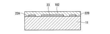
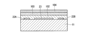
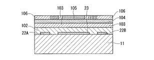
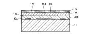
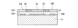
- the infrared sensor of the third embodiment is shown in FIG.
- the infrared sensor 1C shown in FIG. 19 is a bolometer-type infrared sensor which is a type of thermal infrared sensor.
- the infrared sensor 1C includes a base substrate 11, a bolometer infrared light receiver 12, a first beam 13A, a second beam 13B, a first wiring 20A, a second wiring 20B, and an infrared reflecting film 23.
- the first beam 13A and the second beam 13B respectively have connecting portions 16A and 16B connected to the base substrate 11.
- Each of the first beam 13 ⁇ /b>A and the second beam 13 ⁇ /b>B has a separating portion 17 that is separated from the base substrate 11.
Abstract
Provided in the present disclosure is technology that further increases the sensitivity of an infrared sensor. The infrared sensor according to the present disclosure comprises: a base substrate; an infrared light-receiving part; a first beam; a second beam; a first wiring; a second wiring; and an infrared reflecting film. Each of the first beam and the second beam comprises a connection part connected to the base substrate and/or a member on the base substrate, and an estranged part that is estranged from the base substrate, the first and second beam being physically connected to the infrared light-receiving part by the estranged parts. The infrared light-receiving part is supported, by the first beam and the second beam, so as to be estranged from the base substrate, and comprises a lower electrode, an upper electrode and a resistance change film. The resistance change film is sandwiched, in the thickness direction, by the lower electrode and the upper electrode, the lower electrode and the upper electrode are each electrically connected to the resistance change film, the lower electrode and the upper electrode are electrically connected to the first wiring and the second wiring, respectively, at least one electrode among the lower electrode and the upper electrode has a line and space structure, and the infrared reflecting film is provided in a location, within the base substrate surface, facing the infrared light-receiving part.
Description
本開示は、赤外線センサ及び赤外線センサアレイに関する。
The present disclosure relates to an infrared sensor and an infrared sensor array.
赤外線センサの分野において、梁を用いてベース基板から赤外線受光部を離間させる構造が提案されている。この構造は、ベース基板からの赤外線受光部の熱的な絶縁を目的としている。この構造を有する赤外線センサでは、梁の断熱性能が高いほど赤外線の受光感度が向上する。特許文献1は、フォノニック結晶構造の導入によって梁の断熱性能を高める技術を開示している。
In the field of infrared sensors, a structure has been proposed in which a beam is used to separate the infrared light receiving portion from the base substrate. This structure is intended to thermally insulate the infrared light receiving portion from the base substrate. In the infrared sensor having this structure, the higher the heat insulation performance of the beam, the higher the infrared light receiving sensitivity. Patent Document 1 discloses a technique of enhancing the heat insulating performance of a beam by introducing a phononic crystal structure.
赤外線センサの一種に、ボロメータ型センサがある。ボロメータ型センサは、サーミスタ型センサとも称される。ボロメータ型センサの赤外線受光部は、温度によって電気抵抗が変化する抵抗変化材料を含む。特許文献1の開示する赤外線センサには、ボロメータ型センサが含まれる。
A type of infrared sensor is a bolometer type sensor. The bolometer type sensor is also called a thermistor type sensor. The infrared light receiving portion of the bolometer type sensor includes a resistance change material whose electric resistance changes with temperature. The infrared sensor disclosed in Patent Document 1 includes a bolometer type sensor.
非特許文献1には、下部電極と、上部電極と、抵抗変化材料からなる抵抗変化膜とを含む赤外線受光部を備えるボロメータ型赤外線センサが開示されている。非特許文献1の赤外線センサは、下部電極及び上部電極によって抵抗変化膜が厚さ方向に挟持された「サンドイッチ構造」を有する。
Non-Patent Document 1 discloses a bolometer-type infrared sensor including an infrared light receiving portion including a lower electrode, an upper electrode, and a resistance change film made of a resistance change material. The infrared sensor of Non-Patent Document 1 has a "sandwich structure" in which a resistance change film is sandwiched in the thickness direction by a lower electrode and an upper electrode.
本開示は、ボロメータ型赤外線センサにおける赤外線の受光感度を高める技術を提供する。
The present disclosure provides a technique for increasing the infrared light receiving sensitivity of a bolometer-type infrared sensor.
本開示は、以下の赤外線センサを提供する。
赤外線センサであって、
ボロメータ赤外線受光部;
第1梁;
第2梁;
第1配線;
第2配線;及び
赤外線反射膜;
を具備し、
ここで、
前記第1梁及び前記第2梁の各々は、前記ベース基板、及び/又は前記ベース基板上の部材と接続された接続部と、前記ベース基板から離間した離間部と、を有し、かつ、前記離間部において前記赤外線受光部と物理的に接合され、
前記赤外線受光部は、前記第1梁及び前記第2梁によって、前記ベース基板とは離間した状態で支持されており、
前記赤外線受光部は、下部電極と、上部電極と、温度によって電気抵抗が変化する抵抗変化材料から構成される抵抗変化膜と、を含み、
前記抵抗変化膜は、前記下部電極及び前記上部電極によって厚さ方向に挟持され、
前記下部電極及び前記上部電極の各々は、前記抵抗変化膜と電気的に接続され、
前記下部電極及び前記上部電極は、前記第1配線及び前記第2配線と、それぞれ電気的に接続され、
前記下部電極及び前記上部電極から選ばれる少なくとも1つの電極が、ラインアンドスペース構造を有し、
前記赤外線反射膜は、前記ベース基板の表面における前記赤外線受光部に対面する位置に設けられている。 The present disclosure provides the following infrared sensor.
An infrared sensor,
Bolometer infrared receiver;
First beam;
Second beam;
First wiring;
Second wiring; and infrared reflection film;
Equipped with,
here,
Each of the first beam and the second beam has a connecting portion connected to the base substrate and/or a member on the base substrate, and a spacing portion spaced from the base substrate, and Physically joined to the infrared light receiving portion in the separated portion,
The infrared light receiving unit is supported by the first beam and the second beam in a state of being separated from the base substrate,
The infrared light receiving unit includes a lower electrode, an upper electrode, and a resistance change film made of a resistance change material whose electric resistance changes with temperature,
The resistance change film is sandwiched in the thickness direction by the lower electrode and the upper electrode,
Each of the lower electrode and the upper electrode is electrically connected to the resistance change film,
The lower electrode and the upper electrode are electrically connected to the first wiring and the second wiring, respectively.
At least one electrode selected from the lower electrode and the upper electrode has a line and space structure,
The infrared reflective film is provided on the surface of the base substrate at a position facing the infrared light receiving portion.
本開示の赤外線センサは、赤外線の高い受光感度を有しうるボロメータ型センサである。
The infrared sensor of the present disclosure is a bolometer-type sensor that can have high infrared light reception sensitivity.
(本開示の基礎となった知見)
本発明者らの検討によれば、ボロメータ型赤外線センサにおける赤外線の受光感度は、梁の断熱性能の向上だけではなく、熱雑音Nthermの低減によっても向上する。熱雑音Nthermは、赤外線センサの全電気抵抗Rallの1/2乗に比例するパラメータである。本開示の赤外線センサの赤外線受光部は、下部電極と上部電極と抵抗変化膜とを含み、かつ下部電極及び上部電極によって抵抗変化膜が厚さ方向に挟持された構造を有する。当該構造によれば、抵抗変化膜における電流の経路の断面積を広く、経路長を短くすることが可能となる。このため、抵抗変化膜の電気抵抗を低減できる。抵抗変化膜の電気抵抗の低減は、赤外線センサの全電気抵抗Rallを下げ、熱雑音Nthermを低減させる。即ち、上記構造により、赤外線の受光感度の向上が期待される。 (Findings that form the basis of this disclosure)
According to the study by the present inventors, the infrared ray receiving sensitivity of the bolometer-type infrared sensor is improved not only by improving the thermal insulation performance of the beam but also by reducing the thermal noise N therm . The thermal noise N therm is a parameter proportional to the 1/2 electric power of the total electrical resistance R all of the infrared sensor. The infrared light receiving portion of the infrared sensor of the present disclosure has a structure including a lower electrode, an upper electrode, and a resistance change film, and the resistance change film is sandwiched by the lower electrode and the upper electrode in the thickness direction. According to this structure, it is possible to widen the cross-sectional area of the current path in the resistance change film and shorten the path length. Therefore, the electric resistance of the resistance change film can be reduced. The reduction of the electrical resistance of the resistance change film lowers the total electrical resistance R all of the infrared sensor and reduces the thermal noise N therm . That is, the above structure is expected to improve the sensitivity of receiving infrared rays.
一方で、ボロメータ型赤外線センサでは、赤外線受光部における赤外線の吸収量の増大を目的として、ベース基板の表面における赤外線受光部に対面する位置に赤外線反射膜が、通常、設けられる。また、赤外線反射膜の単なる配置のみならず、赤外線反射膜と赤外線受光部との離間距離を制御することにより、外部から赤外線受光部に入射する赤外線、赤外線受光部の上面において反射する赤外線、及び赤外線反射膜において反射して、ベース基板側から赤外線受光部に入射する赤外線の位相の整合が図られている。この位相の整合は、赤外線の吸収量の増大にとって重要である。本発明者らの検討によれば、抵抗変化膜上に面状に拡がった下部電極及び上部電極を上記構造に使用した場合、下部電極と上部電極との間における赤外線の多重反射により、上記位相の整合が困難となる。これに対して、本開示の赤外線センサの赤外線受光部では、下部電極及び上部電極から選ばれる少なくとも1つの電極が、ラインアンドスペース構造(L/S構造)を有する。L/S構造を有する電極では、複数の帯状部が特定の整列方向に互いに離間して整列している。このため、L/S構造を有する電極を透過及び反射する赤外線の主たる成分を、上記整列方向に振動面を有する偏光とすることができる。これは上記赤外線の多重反射を緩和させ、それ故に、上記位相の整合による赤外線の吸収量の増大を図ることができる。したがって、本開示の赤外線センサは高い受光感度を有しうる。
On the other hand, in a bolometer-type infrared sensor, an infrared reflective film is usually provided on the surface of the base substrate at a position facing the infrared light receiving portion in order to increase the amount of infrared light absorbed in the infrared light receiving portion. Further, not only the mere arrangement of the infrared reflecting film, but by controlling the separation distance between the infrared reflecting film and the infrared receiving section, infrared rays incident on the infrared receiving section from the outside, infrared rays reflected on the upper surface of the infrared receiving section, and The phase of infrared rays reflected by the infrared reflecting film and incident on the infrared receiving section from the base substrate side is matched. This phase matching is important for increasing the absorption of infrared rays. According to the study of the present inventors, when the lower electrode and the upper electrode spread in a plane shape on the resistance change film are used in the above structure, the phase shift is caused by the multiple reflection of infrared rays between the lower electrode and the upper electrode. Becomes difficult to match. On the other hand, in the infrared light receiving portion of the infrared sensor of the present disclosure, at least one electrode selected from the lower electrode and the upper electrode has a line and space structure (L/S structure). In the electrode having the L/S structure, a plurality of strip-shaped portions are aligned in a specific alignment direction while being separated from each other. For this reason, the main component of the infrared light that transmits and reflects through the electrode having the L/S structure can be polarized light having a vibrating surface in the alignment direction. This alleviates the multiple reflection of the infrared rays, and therefore, the absorption amount of the infrared rays due to the phase matching can be increased. Therefore, the infrared sensor of the present disclosure may have high light receiving sensitivity.
(本開示の実施形態)
以下、本開示の実施形態について、図面を参照しながら説明する。なお、以下で説明する実施形態は、いずれも包括的、又は具体的な例を示すものである。以下の実施形態で示される数値、形状、材料、構成要素、構成要素の配置位置、及び接続形態、プロセス条件、ステップ、ステップの順序等は一例であり、本開示を限定する主旨ではない。また、以下の実施形態における構成要素のうち、最上位概念を示す独立請求項に記載されていない構成要素については、任意の構成要素として説明される。なお、各図は、模式図であり、必ずしも厳密に図示されたものではない。 (Embodiment of the present disclosure)
Hereinafter, embodiments of the present disclosure will be described with reference to the drawings. It should be noted that each of the embodiments described below shows a comprehensive or specific example. Numerical values, shapes, materials, constituent elements, arrangement positions of constituent elements, connection forms, process conditions, steps, order of steps, and the like shown in the following embodiments are examples, and are not intended to limit the present disclosure. Further, among the constituent elements in the following embodiments, the constituent elements that are not described in the independent claim showing the highest concept are described as arbitrary constituent elements. It should be noted that each drawing is a schematic view and is not necessarily strictly illustrated.
[赤外線センサ]
(実施形態1)
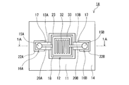
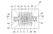
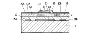
実施形態1の赤外線センサが図1A及び図1Bに示される。図1Aには、図1Bの赤外線センサ1Aの断面1A-1Aが示される。赤外線センサ1Aは、熱型赤外線センサの1種であるボロメータ型赤外線センサである。赤外線センサ1Aは、ベース基板11、ボロメータ赤外線受光部12、第1梁13A、第2梁13B、第1配線20A、第2配線20B、及び赤外線反射膜23を備える。第1梁13A及び第2梁13Bは、それぞれ、ベース基板11上の部材と接続された接続部16A,16Bを有する。第1梁13A及び第2梁13Bの各々は、ベース基板11から離間した離間部17を有する。第1梁13A及び第2梁13Bは、それぞれ、一方の端部に接続部16A,16Bを有している。第1梁13A及び第2梁13Bの各々は、離間部17において赤外線受光部12と物理的に接合されている。赤外線受光部12と物理的に接合されている位置は、第1梁13A及び第2梁13Bの各々における他方の端部である。赤外線受光部12は、第1梁13A及び第2梁13Bによって、ベース基板11とは離間した状態で支持されている。この離間は、ベース基板11と赤外線受光部12との熱的な絶縁を高めている。 [Infrared sensor]
(Embodiment 1)
The infrared sensor ofEmbodiment 1 is shown in FIGS. 1A and 1B. 1A shows a cross section 1A-1A of the infrared sensor 1A of FIG. 1B. The infrared sensor 1A is a bolometer type infrared sensor, which is a type of thermal infrared sensor. The infrared sensor 1A includes a base substrate 11, a bolometer infrared light receiving portion 12, a first beam 13A, a second beam 13B, a first wiring 20A, a second wiring 20B, and an infrared reflecting film 23. The first beam 13A and the second beam 13B respectively have connecting portions 16A and 16B connected to the members on the base substrate 11. Each of the first beam 13</b>A and the second beam 13</b>B has a separating portion 17 that is separated from the base substrate 11. The first beam 13A and the second beam 13B each have connecting portions 16A and 16B at one end. Each of the first beam 13</b>A and the second beam 13</b>B is physically joined to the infrared light receiving section 12 at the spacing section 17. The position that is physically joined to the infrared light receiving unit 12 is the other end of each of the first beam 13A and the second beam 13B. The infrared light receiving portion 12 is supported by the first beam 13A and the second beam 13B while being separated from the base substrate 11. This separation enhances thermal insulation between the base substrate 11 and the infrared light receiving portion 12.
(実施形態1)
実施形態1の赤外線センサが図1A及び図1Bに示される。図1Aには、図1Bの赤外線センサ1Aの断面1A-1Aが示される。赤外線センサ1Aは、熱型赤外線センサの1種であるボロメータ型赤外線センサである。赤外線センサ1Aは、ベース基板11、ボロメータ赤外線受光部12、第1梁13A、第2梁13B、第1配線20A、第2配線20B、及び赤外線反射膜23を備える。第1梁13A及び第2梁13Bは、それぞれ、ベース基板11上の部材と接続された接続部16A,16Bを有する。第1梁13A及び第2梁13Bの各々は、ベース基板11から離間した離間部17を有する。第1梁13A及び第2梁13Bは、それぞれ、一方の端部に接続部16A,16Bを有している。第1梁13A及び第2梁13Bの各々は、離間部17において赤外線受光部12と物理的に接合されている。赤外線受光部12と物理的に接合されている位置は、第1梁13A及び第2梁13Bの各々における他方の端部である。赤外線受光部12は、第1梁13A及び第2梁13Bによって、ベース基板11とは離間した状態で支持されている。この離間は、ベース基板11と赤外線受光部12との熱的な絶縁を高めている。 [Infrared sensor]
(Embodiment 1)
The infrared sensor of
赤外線センサ1Aは、ベース基板11上に配置された部材であって、ベース基板11の上面14から離れる方向に延びる第1支柱15A及び第2支柱15Bをさらに備える。第1支柱15A及び第2支柱15Bは、ベース基板11上の部材である。第1梁13Aは、接続部16Aにおいて第1支柱15Aに物理的に接続されている。第2梁13Bは、接続部16Bにおいて第2支柱15Bと物理的に接続されている。断面視において、赤外線受光部12、第1梁13A、及び第2梁13Bは、第1支柱15A及び第2支柱15Bによってベース基板11の上部で懸架されている。図1A及び図1Bに示される赤外線センサ1Aでは、第1支柱15A及び第2支柱15Bによる上記懸架によって、ベース基板11と赤外線受光部12との離間が達成されている。
The infrared sensor 1A is a member arranged on the base substrate 11 and further includes a first support column 15A and a second support column 15B extending in a direction away from the upper surface 14 of the base substrate 11. The first support columns 15A and the second support columns 15B are members on the base substrate 11. The first beam 13A is physically connected to the first support column 15A at the connecting portion 16A. The second beam 13B is physically connected to the second support column 15B at the connecting portion 16B. In the cross-sectional view, the infrared light receiving portion 12, the first beam 13A, and the second beam 13B are suspended above the base substrate 11 by the first support column 15A and the second support column 15B. In the infrared sensor 1A shown in FIGS. 1A and 1B, the base substrate 11 and the infrared light receiving portion 12 are separated from each other by the suspension by the first support pillar 15A and the second support pillar 15B.
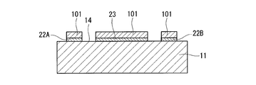
赤外線受光部12は、下部電極31と、上部電極32と、温度によって電気抵抗が変化する抵抗変化材料から構成される抵抗変化膜33とを含む。抵抗変化膜33は、下部電極31及び上部電極32によって厚さ方向に挟持されている。下部電極31は、抵抗変化膜33と直接的かつ電気的に接合している。上部電極32は、抵抗変化膜33と直接的かつ電気的に接合している。
The infrared light receiving unit 12 includes a lower electrode 31, an upper electrode 32, and a resistance change film 33 made of a resistance change material whose electric resistance changes with temperature. The resistance change film 33 is sandwiched by the lower electrode 31 and the upper electrode 32 in the thickness direction. The lower electrode 31 is directly and electrically joined to the resistance change film 33. The upper electrode 32 is directly and electrically joined to the resistance change film 33.
第1配線20Aは、第1梁13A上に形成されている。第1配線20Aと下部電極31とは、電気的に接続されている。第1配線20Aと下部電極31とは一体化されている。第2配線20Bは、第2梁13B上に形成されている。第2配線20Bと上部電極32とは、電気的に接続されている。第2配線20Bと上部電極32とは一体化されている。
The first wiring 20A is formed on the first beam 13A. The first wiring 20A and the lower electrode 31 are electrically connected. The first wiring 20A and the lower electrode 31 are integrated. The second wiring 20B is formed on the second beam 13B. The second wiring 20B and the upper electrode 32 are electrically connected. The second wiring 20B and the upper electrode 32 are integrated.
第1支柱15A及び第2支柱15Bは、導電性を有する。第1配線20Aは、第1支柱15Aに電気的に接続されている。第2配線20Bは、第2支柱15Bに電気的に接続されている。第1支柱15A及び第2支柱15Bは、赤外線受光部12に含まれる抵抗変化膜33の抵抗を検出する電流の経路としての機能も有している。
The first support column 15A and the second support column 15B have conductivity. The first wiring 20A is electrically connected to the first support column 15A. The second wiring 20B is electrically connected to the second support column 15B. The first support column 15A and the second support column 15B also have a function as a current path for detecting the resistance of the resistance change film 33 included in the infrared light receiving unit 12.
赤外線センサ1Aでは、抵抗変化膜33の抵抗の読み取りが実施される。読み取りのために、図1A及び図1Bに示される赤外線センサ1Aは、ベース基板11の内部に読み出し集積回路(ROIC);(図示せず)をさらに備えている。赤外線センサ1Aは、ベース基板11の上面14に第1信号読み出し端子22A及び第2信号読み出し端子22Bをさらに備えている。第1支柱15AとROICとは、第1信号読み出し端子22Aを介して電気的に接続されている。第2支柱15BとROICとは、第2信号読み出し端子22Bを介して電気的に接続されている。抵抗変化膜33の抵抗は、下部電極31、上部電極32、第1配線20A、第2配線20B、第1支柱15A、第2支柱15B、第1信号読み出し端子22A、及び第2信号読み出し端子22Bを介して読み取り可能である。なお、抵抗変化膜33を挟んだ第1信号読み出し端子22Aと第2信号読み出し端子22Bとの間の電気抵抗が、上述した全電気抵抗Rallである。赤外線センサ1Aは、抵抗変化膜33の抵抗を読み取るためのさらなる部材を備えていてもよい。
The infrared sensor 1A reads the resistance of the resistance change film 33. For reading, the infrared sensor 1A shown in FIGS. 1A and 1B further includes a read integrated circuit (ROIC); (not shown) inside the base substrate 11. The infrared sensor 1A further includes a first signal read terminal 22A and a second signal read terminal 22B on the upper surface 14 of the base substrate 11. The first support column 15A and the ROIC are electrically connected via the first signal read terminal 22A. The second support column 15B and the ROIC are electrically connected to each other via the second signal read terminal 22B. The resistance of the resistance change film 33 has a lower electrode 31, an upper electrode 32, a first wiring 20A, a second wiring 20B, a first support column 15A, a second support column 15B, a first signal read terminal 22A, and a second signal read terminal 22B. Can be read through. The electric resistance between the first signal read terminal 22A and the second signal read terminal 22B sandwiching the resistance change film 33 is the total electric resistance R all described above. The infrared sensor 1A may include a further member for reading the resistance of the resistance change film 33.
赤外線受光部12に赤外線が入射すると、赤外線受光部12の温度が上昇する。このとき、赤外線受光部12の温度は、熱浴であるベース基板11及びベース基板11上の部材から熱的に絶縁されているほど、大きく上昇する。ボロメータ赤外線受光部12を備える赤外線センサ1Aでは、温度上昇に伴って、抵抗変化膜33の抵抗が変化する。変化した抵抗に対応する電気的な信号をROICで処理して赤外線が検知される。処理によっては、赤外線センサ1Aによる赤外線の強度測定、及び/又は対象物の温度測定が可能である。ただし、本開示の赤外線センサにおいて、赤外線受光部12に含まれる抵抗変化膜33の抵抗の読み取りは、ベース基板11の内部に設けられたROICによる態様に限定されない。
When the infrared ray is incident on the infrared ray receiving section 12, the temperature of the infrared ray receiving section 12 rises. At this time, the temperature of the infrared light receiving unit 12 rises to a greater extent as it is thermally insulated from the base substrate 11 and the members on the base substrate 11 that are the heat bath. In the infrared sensor 1A including the bolometer infrared light receiving unit 12, the resistance of the resistance change film 33 changes as the temperature rises. The infrared signal is detected by processing the electrical signal corresponding to the changed resistance with the ROIC. Depending on the processing, the infrared intensity can be measured by the infrared sensor 1A and/or the temperature of the object can be measured. However, in the infrared sensor of the present disclosure, the reading of the resistance of the resistance change film 33 included in the infrared light receiving unit 12 is not limited to the mode by the ROIC provided inside the base substrate 11.
赤外線センサ1Aは、ベース基板11の表面における赤外線受光部12に対面する位置に赤外線反射膜23をさらに備えている。図1A及び図1Bに示される赤外線センサ1Aでは、赤外線反射膜23はベース基板11の上面14に配置されている。赤外線反射膜23は、外部から赤外線センサ1Aに入射した赤外線を反射する。反射する赤外線には、赤外線受光部12を透過した赤外線が含まれる。赤外線反射膜23において反射した赤外線は、下部電極31の側から赤外線受光部12に入射しうる。平面視において、赤外線受光部12の面積に比べて赤外線反射膜23の面積は大きい。また、平面視において、赤外線反射膜23は、赤外線受光部12を囲むように配置されている。ただし、赤外線反射膜23の具体的な形態は、図1A及び図1Bに示される例に限定されない。なお、本明細書において、「平面視」とは、対象物の主面に垂直な方向から対象物を視ることを意味する。また、「主面」とは、最も広い面積を有する面を意味する。
The infrared sensor 1A further includes an infrared reflection film 23 on the surface of the base substrate 11 at a position facing the infrared light receiving portion 12. In the infrared sensor 1A shown in FIGS. 1A and 1B, the infrared reflection film 23 is arranged on the upper surface 14 of the base substrate 11. The infrared reflection film 23 reflects infrared rays incident on the infrared sensor 1A from the outside. The infrared rays that are reflected include the infrared rays that have passed through the infrared receiver 12. The infrared light reflected by the infrared reflecting film 23 can enter the infrared light receiving portion 12 from the lower electrode 31 side. In plan view, the area of the infrared reflection film 23 is larger than the area of the infrared light receiver 12. Further, the infrared reflection film 23 is arranged so as to surround the infrared light receiving portion 12 in a plan view. However, the specific form of the infrared reflective film 23 is not limited to the example shown in FIGS. 1A and 1B. In addition, in this specification, "plan view" means viewing an object from a direction perpendicular to the main surface of the object. Further, the “main surface” means a surface having the largest area.
図1A及び図1Bに示される赤外線センサ1Aでは、下部電極31及び上部電極32の双方の電極が、L/S構造を有する。当該下部電極31及び上部電極32の各々を構成する金属膜の実効的なシート抵抗(effective sheet resistance)は、100Ω/□以上かつ500Ω/□以下であることが望ましい。この場合、当該金属膜の実効的なシート抵抗は、真空のインピーダンスと整合する。これにより、当該金属膜における赤外線の反射が抑えられ、赤外線の吸収を増大させることができる。ここで、実効的なシート抵抗とは、有効媒質近似に基づいて得られる不連続体のシート抵抗である。この形態では、上記赤外線の多重反射を緩和させる制御の自由度が向上可能である。また、赤外線センサ1Aでは、下部電極31は第1のL/S構造を有し、上部電極32は第2のL/S構造を有する。平面視において、第1のL/S構造の整列方向と、第2のL/S構造の整列方向とは互いに異なっている。この形態では、上記赤外線の多重反射を緩和させる制御の自由度のさらなる向上が可能である。平面視において、第1のL/S構造の整列方向と第2のL/S構造の整列方向とが成す角度は、劣角により表示して、例えば、45度以上であり、60度以上、70度以上、80度以上、さらには85度以上であってもよい。また、当該角度は、80度以上90度以下であってもよい。赤外線センサ1Aでは、平面視において、第1のL/S構造の整列方向と第2のL/S構造の整列方向とは、直交している。なお、本明細書において、「直交」とは、2つの方向が劣角により表示して89度以上90度以下の角度で交わることを意味し、90度で交わっていてもよい。
In the infrared sensor 1A shown in FIGS. 1A and 1B, both the lower electrode 31 and the upper electrode 32 have an L/S structure. The effective sheet resistance of the metal film forming each of the lower electrode 31 and the upper electrode 32 is preferably 100Ω/□ or more and 500Ω/□ or less. In this case, the effective sheet resistance of the metal film matches the impedance of the vacuum. Thereby, reflection of infrared rays on the metal film can be suppressed, and absorption of infrared rays can be increased. Here, the effective sheet resistance is the sheet resistance of the discontinuous body obtained based on the effective medium approximation. In this form, the degree of freedom of control for alleviating the multiple reflection of infrared rays can be improved. In the infrared sensor 1A, the lower electrode 31 has the first L/S structure and the upper electrode 32 has the second L/S structure. In a plan view, the alignment direction of the first L/S structure and the alignment direction of the second L/S structure are different from each other. In this form, it is possible to further improve the degree of freedom of control for alleviating the multiple reflection of infrared rays. In plan view, the angle formed by the alignment direction of the first L/S structure and the alignment direction of the second L/S structure is displayed as an inferior angle, for example, 45 degrees or more, 60 degrees or more, It may be 70 degrees or more, 80 degrees or more, and even 85 degrees or more. The angle may be 80 degrees or more and 90 degrees or less. In the infrared sensor 1A, the alignment direction of the first L/S structure and the alignment direction of the second L/S structure are orthogonal to each other in a plan view. In the present specification, “orthogonal” means that two directions are displayed as an inferior angle and intersect at an angle of 89 degrees or more and 90 degrees or less, and may intersect at 90 degrees.
L/S構造は、特定の整列方向に互いに離間して整列している2以上の帯状部から構成される構造である。各々の帯状部のライン幅は、通常、等しい。3以上の帯状部からL/S構造が構成される場合、隣接する帯状部の間の各間隔は、通常、等しい。L/S構造において、ライン幅と間隔とが等しくてもよい。
The L/S structure is a structure that is composed of two or more strip-shaped portions that are spaced apart from each other and aligned in a specific alignment direction. The line width of each strip is usually the same. When the L/S structure is composed of three or more strips, the intervals between adjacent strips are usually equal. In the L/S structure, the line width and the spacing may be equal.
下部電極31及び/又は上部電極32が有しうるL/S構造のライン幅及び間隔は、1μm以下であってもよい。当該ライン幅及び間隔の下限は、例えば30nm以上である。赤外線センサ1Aへの入射が想定される赤外線の中心波長の1/10が1μmに相当する。このため、L/S構造のライン幅及び間隔が1μm以下である場合には、当該L/S構造を有する下部電極31及び/又は上部電極32における赤外線に対する偏光選択能が向上可能となる。なお、ライン幅及び間隔が1μm以下であるL/S構造は、赤外線に対するワイヤーグリッド構造と捉えることもできる。
The line width and spacing of the L/S structure that the lower electrode 31 and/or the upper electrode 32 may have may be 1 μm or less. The lower limit of the line width and the interval is, for example, 30 nm or more. 1/10 of the center wavelength of infrared rays that is supposed to be incident on the infrared sensor 1A corresponds to 1 μm. Therefore, when the line width and the spacing of the L/S structure are 1 μm or less, the polarization selectivity of infrared rays in the lower electrode 31 and/or the upper electrode 32 having the L/S structure can be improved. The L/S structure having a line width and an interval of 1 μm or less can also be regarded as a wire grid structure for infrared rays.
下部電極31が有しうる第1のL/S構造と、上部電極32が有しうる第2のL/S構造とは、同一のライン幅及び間隔を有していてもよい。この形態では、上記赤外線の多重反射を緩和させる制御の自由度のさらなる向上が可能である。また、第1のL/S構造と第2のL/S構造とが同一のライン幅及び間隔を有するとともに、第1のL/S構造の整列方向と第2のL/S構造の整列方向とが平面視において直交する場合、当該自由度は特に高くなりうる。
The first L/S structure that the lower electrode 31 may have and the second L/S structure that the upper electrode 32 may have may have the same line width and spacing. In this form, it is possible to further improve the degree of freedom of control for alleviating the multiple reflection of infrared rays. Further, the first L/S structure and the second L/S structure have the same line width and the same space, and the alignment direction of the first L/S structure and the alignment direction of the second L/S structure. When and are orthogonal to each other in a plan view, the degree of freedom can be particularly high.
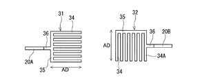
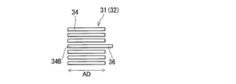
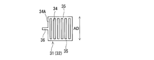
図1A及び図1Bの赤外線センサ1Aにおける下部電極31及び上部電極32が、図2に示される。図2の下部電極31及び上部電極32は、特定の一つの整列方向ADに延びる7つの帯状部34を有する。7つの帯状部34は、各々の一方の端部において、バスライン35により物理的かつ電気的に接続されている。また、下部電極31では、接続ライン36が、バスライン35から、帯状部34の配列している側とは反対側、かつ整列方向ADに平行に延びている。接続ライン36には帯状の第1配線20Aが接続されており、下部電極31と第1配線20Aとは一体化されている。第1配線20Aの延びる方向は、整列方向ADに平行である。上部電極32では、配列の端に位置する帯状部34Aから、帯状部34の配列している側とは反対側、かつ整列方向ADに垂直に接続ライン36が延びている。接続ライン36には第2配線20Bが接続されており、上部電極32と第2配線20Bとは一体化されている。第2配線20Bの延びる方向は、整列方向ADに垂直である。下部電極31の構造と、上部電極32の構造とは逆であってもよい。換言すれば、下部電極31が図2に示される上部電極32の構造を有し、上部電極32が図2に示される下部電極31の構造を有していてもよい。
The lower electrode 31 and the upper electrode 32 in the infrared sensor 1A of FIGS. 1A and 1B are shown in FIG. The lower electrode 31 and the upper electrode 32 in FIG. 2 have seven strip portions 34 extending in one specific alignment direction AD. The seven strips 34 are physically and electrically connected to each other at one end by a bus line 35. In the lower electrode 31, the connection line 36 extends from the bus line 35 on the side opposite to the side where the strip portions 34 are arranged and in parallel to the alignment direction AD. The strip-shaped first wiring 20A is connected to the connection line 36, and the lower electrode 31 and the first wiring 20A are integrated. The extending direction of the first wiring 20A is parallel to the alignment direction AD. In the upper electrode 32, the connection line 36 extends from the strip-shaped portion 34A located at the end of the array, on the side opposite to the side where the strip-shaped portions 34 are arrayed and perpendicular to the alignment direction AD. The second wiring 20B is connected to the connection line 36, and the upper electrode 32 and the second wiring 20B are integrated. The extending direction of the second wiring 20B is perpendicular to the alignment direction AD. The structure of the lower electrode 31 and the structure of the upper electrode 32 may be reversed. In other words, the lower electrode 31 may have the structure of the upper electrode 32 shown in FIG. 2, and the upper electrode 32 may have the structure of the lower electrode 31 shown in FIG.
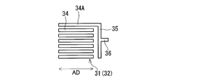
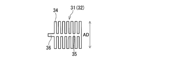
下部電極31及び上部電極32のさらなる例が、図3A、図3B、図3C、図3D及び図3Eに示される。図3A、図3B、図3C、図3D及び図3Eの下部電極31及び/又は上部電極32は、特定の一つの整列方向ADに延びる7つの帯状部34を有する。図3Aの下部電極31及び/又は上部電極32では、各々の帯状部34は物理的にも電気的にも接続されていない。ただし、配列の端に位置する帯状部34Aから、帯状部34の配列している側とは反対側、かつ整列方向ADに垂直に接続ライン36が延びている。図3Aに示されるように、各々の帯状部34が物理的にも電気的にも接続されていない場合においても、当該L/S構造を有する電極は、赤外線に対する偏光選択能を有しうる。また、接続ライン36が電気的に接続された帯状部34Aの存在により、当該電極は、抵抗変化膜33の電気抵抗を測定するための電極として機能できる。図3Bの下部電極31及び/又は上部電極32では、各々の帯状部34は物理的にも電気的にも接続されていない。ただし、配列の端に位置する帯状部34Aの一端にはバスライン35が接続されている。また、バスライン35から、帯状部34の配列している側とは反対側、かつ整列方向ADに平行に接続ライン36が接続されている。図3Cの下部電極31及び/又は上部電極32では、各々の帯状部34が、その中央部において、バスライン35により物理的かつ電気的に接続されている。また、バスライン35の一端は接続ライン36を構成している。図3Dの下部電極31及び/又は上部電極32では、各々の帯状部34は物理的にも電気的にも接続されていない。ただし、配列の中央に位置する帯状部34Bの一端に接続ライン36が接続されている。図3Eの下部電極31及び/又は上部電極32では、各々の帯状部34の双方の端部が、それぞれバスライン35により物理的かつ電気的に接続されている。また、配列の端に位置する帯状部34Aから、帯状部34の配列している側とは反対側、かつ整列方向ADに垂直に接続ライン36が延びている。
Further examples of bottom electrode 31 and top electrode 32 are shown in FIGS. 3A, 3B, 3C, 3D and 3E. The lower electrode 31 and/or the upper electrode 32 of FIGS. 3A, 3B, 3C, 3D, and 3E has seven strips 34 extending in one specific alignment direction AD. In the lower electrode 31 and/or the upper electrode 32 of FIG. 3A, the strip portions 34 are not physically or electrically connected. However, the connection line 36 extends from the strip-shaped portion 34A located at the end of the array, on the side opposite to the side where the strip-shaped portions 34 are arrayed and perpendicular to the alignment direction AD. As shown in FIG. 3A, even when the strip-shaped portions 34 are not physically or electrically connected to each other, the electrode having the L/S structure can have polarization selection ability with respect to infrared rays. Further, due to the existence of the strip-shaped portion 34A to which the connection line 36 is electrically connected, the electrode can function as an electrode for measuring the electric resistance of the resistance change film 33. In the lower electrode 31 and/or the upper electrode 32 of FIG. 3B, the strip portions 34 are not physically or electrically connected to each other. However, the bus line 35 is connected to one end of the strip portion 34A located at the end of the array. A connection line 36 is connected from the bus line 35 to the side opposite to the side where the strip portions 34 are arranged and parallel to the alignment direction AD. In the lower electrode 31 and/or the upper electrode 32 of FIG. 3C, each strip|belt-shaped part 34 is physically and electrically connected by the bus line 35 in the center part. Further, one end of the bus line 35 constitutes a connection line 36. In the lower electrode 31 and/or the upper electrode 32 of FIG. 3D, the respective strip portions 34 are not physically or electrically connected. However, the connection line 36 is connected to one end of the strip portion 34B located in the center of the array. In the lower electrode 31 and/or the upper electrode 32 of FIG. 3E, both ends of each strip 34 are physically and electrically connected by a bus line 35. Further, the connection line 36 extends from the strip-shaped portion 34A located at the end of the array, on the side opposite to the side where the strip-shaped portions 34 are arrayed and perpendicular to the alignment direction AD.
下部電極31及び上部電極32の厚さは、例えば、30~500nmである。
The thickness of the lower electrode 31 and the upper electrode 32 is, for example, 30 to 500 nm.
本開示の赤外線センサが有しうる下部電極31及び上部電極32は、上記例に限定されない。
The lower electrode 31 and the upper electrode 32 that can be included in the infrared sensor of the present disclosure are not limited to the above example.
図1A及び図1Bに示される赤外線センサ1Aでは、赤外線受光部12は、受光部支持膜18をさらに備える。受光部支持膜18は、第1梁13A及び第2梁13Bに物理的に接続されている。上記接続により、第1梁13A、第2梁13B、第1支柱15A、及び第2支柱15Bによる上記懸架構造が達成される。また、赤外線センサ1Aでは、受光部支持膜18、第1梁13A、及び第2梁13Bは、一つの半導体層21により構成されている。半導体層21は、単層である。ただし、半導体層21は2以上の層の積層構造を有していてもよい。また、本開示の赤外線センサにおける、第1梁13A、第2梁13B、第1支柱15A、及び第2支柱15Bを用いた赤外線受光部12の懸架構造は上記例に限定されない。
In the infrared sensor 1A shown in FIGS. 1A and 1B, the infrared light receiving section 12 further includes a light receiving section support film 18. The light receiving portion support film 18 is physically connected to the first beam 13A and the second beam 13B. With the above connection, the above-mentioned suspension structure by the first beam 13A, the second beam 13B, the first support column 15A, and the second support column 15B is achieved. Further, in the infrared sensor 1A, the light receiving portion support film 18, the first beam 13A, and the second beam 13B are configured by one semiconductor layer 21. The semiconductor layer 21 is a single layer. However, the semiconductor layer 21 may have a laminated structure of two or more layers. Further, in the infrared sensor of the present disclosure, the suspension structure of the infrared light receiving unit 12 using the first beam 13A, the second beam 13B, the first support column 15A, and the second support column 15B is not limited to the above example.
赤外線センサ1Aでは、平面視において、抵抗変化膜33の面積に比べて受光部下地膜18の面積は大きい。また、平面視において、受光部下地膜18は、抵抗変化膜33を囲むように配置されている。ただし、受光部下地膜18の具体的な形態は、図1A及び図1Bに示される例に限定されない。
In the infrared sensor 1A, the area of the light receiving portion base film 18 is larger than the area of the resistance change film 33 in plan view. Further, the light receiving portion base film 18 is arranged so as to surround the resistance change film 33 in a plan view. However, the specific form of the light-receiving part base film 18 is not limited to the example shown in FIGS. 1A and 1B.
ベース基板11は、典型的には、半導体から構成される。半導体は、例えば、シリコン(Si)である。Siから構成されるベース基板11の上面14には、酸化膜が形成されていてもよい。酸化膜は、例えばSiO2膜である。ただし、ベース基板11の構成は、上記例に限定されない。
The base substrate 11 is typically composed of a semiconductor. The semiconductor is, for example, silicon (Si). An oxide film may be formed on the upper surface 14 of the base substrate 11 made of Si. The oxide film is, for example, a SiO 2 film. However, the configuration of the base substrate 11 is not limited to the above example.
ROICは、公知の構成を有しうる。ROICは、ベース基板11の内部とは異なる場所に設けられていてもよい。ROICは、例えば、ベース基板11の上面14に設けられてもよい。
ROIC may have a known configuration. The ROIC may be provided in a place different from the inside of the base substrate 11. The ROIC may be provided on the upper surface 14 of the base substrate 11, for example.
第1の支柱15A、第2の支柱15B、第1信号読み出し端子22A、及び第2信号読み出し端子22Bは、例えば、不純物がドープされた半導体、又は金属から構成される。金属は、例えば、チタン(Ti)又は窒化チタン(TiN)といった低熱伝導率の種である。金属は、アルミニウム(Al)であってもよい。ただし、第1の支柱15A、第2の支柱15B、及び信号読み出し端子22A,22Bを構成する材料は、上記例に限定されない。
The first support column 15A, the second support column 15B, the first signal read terminal 22A, and the second signal read terminal 22B are made of, for example, a semiconductor doped with impurities or a metal. The metal is a low thermal conductivity species such as titanium (Ti) or titanium nitride (TiN). The metal may be aluminum (Al). However, the materials forming the first support column 15A, the second support column 15B, and the signal read terminals 22A and 22B are not limited to the above examples.
第1梁13A及び第2梁13Bは、例えば、半導体又は酸化物から構成される。半導体は、例えば、Si、シリコンゲルマニウム(SiGe)、窒化ケイ素(SiN)である。酸化物は、例えば、酸化バナジウムである。第1梁13A及び第2梁13Bは、Si又は酸化バナジウムから構成されてもよい。ただし、第1梁13A及び第2梁13Bを構成する材料は、上記例に限定されない。
The first beam 13A and the second beam 13B are made of, for example, a semiconductor or an oxide. The semiconductor is, for example, Si, silicon germanium (SiGe), or silicon nitride (SiN). The oxide is, for example, vanadium oxide. The first beam 13A and the second beam 13B may be made of Si or vanadium oxide. However, the material forming the first beam 13A and the second beam 13B is not limited to the above example.
受光部支持膜18は、例えば、半導体から構成される。半導体は、例えば、Si、SiGe、SiNである。受光部支持膜18の導電性は低いことが望ましい。低い導電性を有する半導体として、非晶質の半導体が選択可能である。ただし、受光部支持膜18を構成する材料は、上記例に限定されない。
The light receiving section support film 18 is made of, for example, a semiconductor. The semiconductor is, for example, Si, SiGe, or SiN. It is desirable that the light-receiving part support film 18 has low conductivity. An amorphous semiconductor can be selected as a semiconductor having low conductivity. However, the material forming the light receiving portion support film 18 is not limited to the above example.
下部電極31、上部電極32、第1配線20A、及び第2配線20Bは、導電性を有する。下部電極31、上部電極32、第1配線20A、及び第2配線20Bは、例えば、不純物がドープされた半導体、又は金属から構成される。金属は、例えば、Ti又はTiNといった低熱伝導率の種である。ただし、下部電極31、上部電極32、第1配線20A、及び第2配線20Bを構成する材料は、上記例に限定されない。
The lower electrode 31, the upper electrode 32, the first wiring 20A, and the second wiring 20B have conductivity. The lower electrode 31, the upper electrode 32, the first wiring 20A, and the second wiring 20B are made of, for example, a semiconductor doped with impurities or a metal. The metal is a low thermal conductivity species such as Ti or TiN. However, the material forming the lower electrode 31, the upper electrode 32, the first wiring 20A, and the second wiring 20B is not limited to the above example.
抵抗変化膜33に含まれる抵抗変化材料は、例えば、半導体又は酸化物から構成される。半導体は、例えば、Si、SiGeである。酸化物は、例えば、酸化バナジウムである。抵抗変化膜33は、Si又は酸化バナジウムから構成されてもよい。抵抗変化膜33の導電性は低いことが望ましい。低い導電性を有する半導体として、非晶質の半導体が選択可能である。抵抗変化膜33は、例えば、非晶質のSiから構成される。ただし、抵抗変化材料は上記例に限定されない。
The resistance change material contained in the resistance change film 33 is made of, for example, a semiconductor or an oxide. The semiconductor is, for example, Si or SiGe. The oxide is, for example, vanadium oxide. The resistance change film 33 may be made of Si or vanadium oxide. It is desirable that the resistance change film 33 have low conductivity. An amorphous semiconductor can be selected as a semiconductor having low conductivity. The resistance change film 33 is made of, for example, amorphous Si. However, the resistance change material is not limited to the above example.
赤外線反射膜23は、典型的には、金属から構成される。金属は、例えば、クロム(Cr)、Al、金(Au)である。ただし、赤外線反射膜23を構成する材料は、上記例に限定されない。
The infrared reflective film 23 is typically made of metal. The metal is, for example, chromium (Cr), Al, or gold (Au). However, the material forming the infrared reflective film 23 is not limited to the above example.
第1梁13Aにおける、赤外線受光部12との接合部と接続部16Aとの間に位置する区間、及び/又は第2梁13Bにおける、赤外線受光部12との接合部と接続部16Bとの間に位置する区間は、規則的に配列した複数の貫通孔を具備するフォノニック結晶構造を有していてもよい。実施形態1の赤外線センサ1Aの一例では、第1梁13Aにおける、赤外線受光部12との接合部と接続部16Aとの間に位置する区間は、規則的に配列した複数の貫通孔を具備する第1フォノニック結晶構造を有し、第2梁13Bにおける、赤外線受光部12との接合部と接続部16Bとの間に位置する区間は、規則的に配列した複数の貫通孔を具備する第2フォノニック結晶構造を有する。上記区間は、通常、第1梁13A及び/又は第2梁13Bの離間部17に位置する。
A section of the first beam 13A located between the joint with the infrared receiver 12 and the connecting portion 16A, and/or between a joint of the second beam 13B with the infrared receiver 12 and the connecting portion 16B. The section located at may have a phononic crystal structure with a plurality of regularly arranged through holes. In an example of the infrared sensor 1A according to the first embodiment, a section of the first beam 13A located between the joint with the infrared receiver 12 and the connecting portion 16A includes a plurality of regularly arranged through holes. The second beam 13B has a first phononic crystal structure, and a section of the second beam 13B located between the joint with the infrared light receiving portion 12 and the connecting portion 16B is provided with a plurality of regularly arranged through holes. It has a phononic crystal structure. The above-mentioned section is usually located in the space 17 of the first beam 13A and/or the second beam 13B.
絶縁体及び半導体において、熱は、主として、フォノンと呼ばれる格子振動によって運ばれる。絶縁体又は半導体から構成される材料の熱伝導率は、材料が有するフォノンの分散関係により決定される。フォノンの分散関係とは、周波数と波数との関係、又はバンド構造を意味している。絶縁体及び半導体において、熱を運ぶフォノンは、100GHzから10THzの幅広い周波数帯域に及ぶ。この周波数帯域は、熱の帯域である。材料の熱伝導率は、熱の帯域にあるフォノンの分散関係により定められる。
In insulators and semiconductors, heat is mainly transferred by lattice vibration called phonons. The thermal conductivity of a material composed of an insulator or a semiconductor is determined by the dispersion relation of phonons contained in the material. The phonon dispersion relation means a relation between frequency and wave number or a band structure. In insulators and semiconductors, heat-carrying phonons cover a wide frequency band from 100 GHz to 10 THz. This frequency band is a heat band. The thermal conductivity of a material is defined by the dispersion relation of phonons in the heat zone.
フォノニック結晶構造によれば、貫通孔の周期構造によって、材料が有するフォノンの分散関係が制御可能である。即ち、フォノニック結晶構造によれば、材料の熱伝導率そのものが制御可能である。とりわけ、フォノニック結晶構造によるフォノニックバンドギャップ(PBG)の形成は、材料の熱伝導率を大きく低減させうる。PBG内にフォノンは存在できない。このため、熱の帯域に位置するPBGは、熱伝導のギャップとなりうる。また、PBG以外の周波数帯域においても、フォノンの分散曲線の傾きがPBGによって小さくなる。傾きの低減はフォノンの群速度を低下させ、熱伝導速度を低下させる。これらの点は、材料の熱伝導率の低減に大きく寄与する。材料の熱伝導率は、例えば、多孔質化により低減できる。多孔質化により導入された空隙が材料の熱伝導率を減少させるためである。しかし、フォノニック結晶構造によれば、材料自身の熱伝導率が低減可能となる。このため、単なる多孔質化に比べて、熱伝導率のさらなる低減が期待される。
According to the phononic crystal structure, the phonon dispersion relationship of the material can be controlled by the periodic structure of the through holes. That is, according to the phononic crystal structure, the thermal conductivity itself of the material can be controlled. In particular, the formation of a phononic bandgap (PBG) with a phononic crystal structure can significantly reduce the thermal conductivity of the material. Phonons cannot exist in PBG. Therefore, the PBG located in the heat zone can be a heat conduction gap. Also, in the frequency bands other than PBG, the slope of the phonon dispersion curve is reduced by PBG. The reduction of the inclination lowers the group velocity of phonons and lowers the heat conduction velocity. These points greatly contribute to the reduction of the thermal conductivity of the material. The thermal conductivity of the material can be reduced, for example, by making it porous. This is because the voids introduced by the porosity decrease the thermal conductivity of the material. However, the phononic crystal structure can reduce the thermal conductivity of the material itself. For this reason, it is expected that the thermal conductivity will be further reduced as compared with the case where the material is simply made porous.
上記説明から理解されるように、フォノニック結晶構造を有する区間を有する第1梁13A及び第2梁13Bでは、熱伝導率のさらなる低減が可能である。したがって、第1梁13A及び/又は第2梁13B、特に第1梁13A及び第2梁13Bの双方、が上記区間にフォノニック結晶構造を有する場合に、赤外線センサ1Aにおけるベース基板11と赤外線受光部12との熱的な絶縁はさらに向上可能となる。また、熱的な絶縁のさらなる向上により、赤外線センサ1Aの受光感度のさらなる向上が可能となる。
As can be understood from the above description, the thermal conductivity can be further reduced in the first beam 13A and the second beam 13B having the section having the phononic crystal structure. Therefore, when the first beam 13A and/or the second beam 13B, especially both the first beam 13A and the second beam 13B have the phononic crystal structure in the above-mentioned section, the base substrate 11 and the infrared light receiving unit in the infrared sensor 1A. The thermal insulation with 12 can be further improved. Further, the thermal insulation is further improved, so that the light receiving sensitivity of the infrared sensor 1A can be further improved.
以下の説明は、第1梁13A及び/又は第2梁13Bが有しうるフォノニック結晶構造に関する。これ以降、第1梁13A及び/又は第2梁13Bが有しうるフォノニック結晶構造は、フォノニック結晶構造Aと記載される。
The following description relates to the phononic crystal structure that the first beam 13A and/or the second beam 13B can have. Hereinafter, the phononic crystal structure that the first beam 13A and/or the second beam 13B may have is described as a phononic crystal structure A.
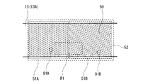
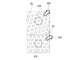
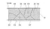
フォノニック結晶構造Aの一例が図4A及び図4Bに示される。図4Aには、梁13(13A)の一部を平面視した状態が示されている。図4Bには、梁13(13B)の一部を平面視した状態が示されている。梁13(13A,13B)は、例えば、10nm以上500nm以下の厚さを有する。梁13は、平面視において、長方形である。梁13の長辺は、赤外線受光部12と接続部16A,16Bとを結ぶ方向、即ち、赤外線センサ1Aにおけるマクロな熱の伝達方向、と一致している。梁13には、梁13の厚さ方向に延びる複数の貫通孔50が設けられている。梁13が有するフォノニック結晶構造Aは、複数の貫通孔50が面内方向に規則的に配列した二次元フォノニック結晶構造である。
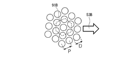
An example of the phononic crystal structure A is shown in FIGS. 4A and 4B. FIG. 4A shows a state in which a part of the beam 13 (13A) is viewed in a plan view. FIG. 4B shows a state in which a part of the beam 13 (13B) is viewed in plan. The beam 13 (13A, 13B) has a thickness of 10 nm or more and 500 nm or less, for example. The beam 13 is rectangular in plan view. The long side of the beam 13 coincides with the direction connecting the infrared light receiving portion 12 and the connection portions 16A and 16B, that is, the macro heat transfer direction in the infrared sensor 1A. The beam 13 is provided with a plurality of through holes 50 extending in the thickness direction of the beam 13. The phononic crystal structure A of the beam 13 is a two-dimensional phononic crystal structure in which a plurality of through holes 50 are regularly arranged in the in-plane direction.
第1の梁13Aのフォノニック結晶構造Aは、フォノニック結晶領域である第1ドメイン51A、及びフォノニック結晶領域である第2ドメイン51Bを有する。第1ドメイン51Aは、平面視において、第1方向に規則的に配列した複数の貫通孔50を具備するフォノニック単結晶構造を有する。第2ドメイン51Bは、平面視において、第1方向とは異なる第2方向に規則的に配列した複数の貫通孔50を具備するフォノニック単結晶構造を有する。各々の単結晶構造内において、複数の貫通孔50の径及び配列周期は同一である。また、各々の単結晶構造内において、規則的に配列した複数の貫通孔50を具備する単位格子91A又は91Bの方位は同一である。第1ドメイン51A及び第2ドメイン51Bの形状は、平面視において、長方形である。第1ドメイン51Aの形状と、第2ドメイン51Bの形状とは、平面視において、同一である。
The phononic crystal structure A of the first beam 13A has a first domain 51A that is a phononic crystal region and a second domain 51B that is a phononic crystal region. The first domain 51A has a phononic single crystal structure including a plurality of through holes 50 regularly arranged in the first direction in a plan view. The second domain 51B has a phononic single crystal structure including a plurality of through holes 50 regularly arranged in a second direction different from the first direction in a plan view. Within each single crystal structure, the diameters and the arrangement period of the plurality of through holes 50 are the same. In addition, in each single crystal structure, the unit lattices 91A or 91B having the plurality of through holes 50 regularly arranged have the same orientation. The shapes of the first domain 51A and the second domain 51B are rectangular in plan view. The shape of the first domain 51A and the shape of the second domain 51B are the same in plan view.
第2の梁13Bのフォノニック結晶構造Aは、フォノニック結晶領域である第3ドメイン51C、及びフォノニック結晶領域である第4ドメイン51Dを有する。第3ドメイン51Cは、平面視において、第3方向に規則的に配列した複数の貫通孔50を具備するフォノニック単結晶構造を有する。第4ドメイン51Dは、平面視において、第3方向とは異なる第4方向に規則的に配列した複数の貫通孔50を具備するフォノニック単結晶構造を有する。各々の単結晶構造内において、複数の貫通孔50の径及び配列周期は同一である。また、各々の単結晶構造内において、規則的に配列した複数の貫通孔50を具備する単位格子91A又は91Bの方位は同一である。第3ドメイン51C及び第4ドメイン51Dの形状は、平面視において、長方形である。第3ドメイン51Cの形状と、第4ドメイン51Dの形状とは、平面視において、同一である。
The phononic crystal structure A of the second beam 13B has a third domain 51C that is a phononic crystal region and a fourth domain 51D that is a phononic crystal region. The third domain 51C has a phononic single crystal structure having a plurality of through holes 50 regularly arranged in the third direction in a plan view. The fourth domain 51D has a phononic single crystal structure including a plurality of through holes 50 regularly arranged in a fourth direction different from the third direction in a plan view. Within each single crystal structure, the diameters and the arrangement period of the plurality of through holes 50 are the same. In addition, in each single crystal structure, the unit lattices 91A or 91B having the plurality of through holes 50 regularly arranged have the same orientation. The shapes of the third domain 51C and the fourth domain 51D are rectangular in plan view. The shape of the third domain 51C and the shape of the fourth domain 51D are the same in plan view.
図4A及び図4Bに示されるフォノニック結晶構造Aは、複数のフォノニック単結晶構造の複合体であるフォノニック多結晶構造52でもある。
The phononic crystal structure A shown in FIGS. 4A and 4B is also a phononic polycrystalline structure 52 which is a composite of a plurality of phononic single crystal structures.
図4Aに示されるフォノニック結晶構造Aと、図4Bに示されるフォノニック結晶構造Aとは同一である。ただし、両者は互いに異なっていてもよい。
The phononic crystal structure A shown in FIG. 4A and the phononic crystal structure A shown in FIG. 4B are the same. However, both may be different from each other.
第1梁13Aが有しうるフォノニック結晶構造Aと、第2梁13Bが有しうるフォノニック結晶構造Aとは、同一であっても、互いに異なっていてもよい。
The phononic crystal structure A that the first beam 13A may have and the phononic crystal structure A that the second beam 13B may have may be the same or different.
以下、フォノニック結晶構造Aがとりうる形態の詳細について、第1梁13Aが有しうるフォノニック結晶構造A、換言すれば、第1ドメイン51A及び第2ドメイン51Bを有するフォノニック結晶構造A、を例に説明する。第2梁13Bが有しうるフォノニック結晶構造Aも、同様の形態をとりうる。第1梁13Aが有しうるフォノニック結晶構造Aと第2梁13Bが有しうるフォノニック結晶構造Aとは、説明する形態の範囲内で互いに異なっていてもよい。
Hereinafter, regarding the details of the form that the phononic crystal structure A can take, the phononic crystal structure A that the first beam 13A can have, in other words, the phononic crystal structure A that has the first domain 51A and the second domain 51B will be taken as an example. explain. The phononic crystal structure A that the second beam 13B may have may have the same form. The phononic crystal structure A that the first beam 13A can have and the phononic crystal structure A that the second beam 13B can have may be different from each other within the scope of the form described.
フォノニック結晶領域であるドメインは、貫通孔50の配列の周期をPとして、平面視において、例えば、25P2以上の面積を有する領域である。フォノニック結晶構造によってフォノンの分散関係を制御するには、ドメインは、少なくとも25P2以上の面積を有していてもよい。平面視において正方形のドメインでは、5×P以上の周期とすることで、25P2以上の面積が確保可能である。
The domain, which is a phononic crystal region, is a region having an area of, for example, 25 P 2 or more in a plan view with the period of the arrangement of the through holes 50 being P. In order to control the phonon dispersion relation by the phononic crystal structure, the domain may have an area of at least 25P 2 . In a square domain in a plan view, an area of 25P 2 or more can be secured by setting a period of 5×P or more.
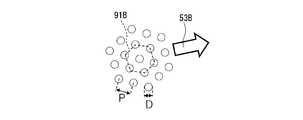
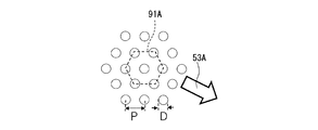
図5A及び図5Bに示すように、フォノニック結晶構造Aでは、第1ドメイン51Aにおける単位格子91Aの方位53Aと、第2ドメイン51Bにおける単位格子91Bの方位53Bとが、平面視において、互いに異なっている。方位53Aと方位53Bとが成す角度は、平面視において、例えば10度以上である。ただし、単位格子91A及び単位格子91Bが同一であって、n回回転対称性を有する場合、方位53Aと方位53Bとが成す角度の上限は360/n度未満である。なお、単位格子が複数のnに対してn回回転対称性を有するとき、上記角度の上限を定めるnには最大のnが使用される。例えば、六方格子は、2回回転対称性、3回回転対称性、及び6回回転対称性を有する。このとき、角度の上限を定めるnには「6」が使用される。即ち、六方格子である単位格子91A,91Bについて、方位53Aと方位53Bとが成す角度は60度未満である。フォノニック結晶構造Aは、単位格子の方位が互いに異なる2以上のフォノニック結晶領域を少なくとも有している。この条件が満たされる限り、フォノニック結晶構造Aは、任意のフォノニック結晶領域、及び/又はフォノニック結晶構造を有さない領域をさらに含んでいてもよい。
As shown in FIGS. 5A and 5B, in the phononic crystal structure A, the orientation 53A of the unit lattice 91A in the first domain 51A and the orientation 53B of the unit lattice 91B in the second domain 51B are different from each other in plan view. There is. The angle formed by the azimuth 53A and the azimuth 53B is, for example, 10 degrees or more in plan view. However, when the unit lattices 91A and 91B are the same and have n-fold rotational symmetry, the upper limit of the angle formed by the azimuths 53A and 53B is less than 360/n degrees. When the unit lattice has n-fold rotational symmetry with respect to a plurality of n, the maximum n is used as n that defines the upper limit of the angle. For example, a hexagonal lattice has 2-fold rotational symmetry, 3-fold rotational symmetry, and 6-fold rotational symmetry. At this time, "6" is used for n that defines the upper limit of the angle. That is, with respect to the unit lattices 91A and 91B that are hexagonal lattices, the angle formed by the azimuth 53A and the azimuth 53B is less than 60 degrees. The phononic crystal structure A has at least two or more phononic crystal regions in which the unit cell orientations are different from each other. As long as this condition is satisfied, the phononic crystal structure A may further include an arbitrary phononic crystal region and/or a region having no phononic crystal structure.
単位格子の方位は、任意の規則に基づいて決定できる。ただし、異なるドメイン間において、同じ規則を適用して単位格子の方位を定める必要がある。単位格子の方位は、例えば、単位格子を構成する平行でない二辺の成す角を二等分する直線の伸長方向である。ただし、異なるドメイン間において、同じ規則で二辺を定める必要がある。
Azimuth of unit cell can be determined based on arbitrary rules. However, it is necessary to apply the same rule between different domains to determine the orientation of the unit cell. The azimuth of the unit cell is, for example, the extending direction of a straight line that bisects the angle formed by two non-parallel sides forming the unit cell. However, it is necessary to define two sides by the same rule between different domains.
図4Aのフォノニック結晶構造Aの領域R1の拡大図が、図6に示される。隣接する第1ドメイン51Aと第2ドメイン51Bとの界面55において、単位格子91A,91Bの方位53A,53Bが変化している。単位格子の方位が変化する界面55は、フォノニック結晶構造Aをマクロに流れる熱に対する大きな界面抵抗をもたらす。この界面抵抗は、第1ドメイン51Aと第2ドメイン51Bとの間で生じる、フォノン群速度のミスマッチに基づく。この界面抵抗は、フォノニック結晶構造Aを有する梁13(13A)における熱伝導率の低減に寄与する。なお、図6において、界面55は、平面視において、直線状に延びている。また、界面55は、平面視において、長方形の梁13の幅方向に延びている。幅方向は、マクロな熱の伝達方向により定められた梁13の中心線の伸張方向に垂直な方向でありうる。界面55は、平面視において、マクロな熱の伝達方向に垂直にフォノニック結晶構造Aを分割している。
An enlarged view of the region R1 of the phononic crystal structure A of FIG. 4A is shown in FIG. At the interface 55 between the first domain 51A and the second domain 51B which are adjacent to each other, the orientations 53A and 53B of the unit lattices 91A and 91B are changed. The interface 55 in which the orientation of the unit cell changes causes a large interface resistance to heat flowing to the macro in the phononic crystal structure A. This interface resistance is based on the phonon group velocity mismatch that occurs between the first domain 51A and the second domain 51B. This interface resistance contributes to the reduction of the thermal conductivity of the beam 13 (13A) having the phononic crystal structure A. In addition, in FIG. 6, the interface 55 extends linearly in a plan view. The interface 55 extends in the width direction of the rectangular beam 13 in a plan view. The width direction may be a direction perpendicular to the extension direction of the center line of the beam 13 defined by the macro heat transfer direction. The interface 55 divides the phononic crystal structure A perpendicularly to the macro heat transfer direction in a plan view.
図4Aのフォノニック結晶構造Aにおいて、第1ドメイン51Aにおける複数の貫通孔50の配列の周期Pと、第2ドメイン51Bにおける複数の貫通孔50の配列の周期Pとは等しい。
In the phononic crystal structure A of FIG. 4A, the period P of the arrangement of the plurality of through holes 50 in the first domain 51A and the period P of the arrangement of the plurality of through holes 50 in the second domain 51B are equal.
図4Aのフォノニック結晶構造Aにおいて、第1ドメイン51Aにおいて規則的に配列した複数の貫通孔50の径と、第2ドメイン51Bにおいて規則的に配列した複数の貫通孔50の径とは等しい。
In the phononic crystal structure A of FIG. 4A, the diameter of the plurality of through holes 50 regularly arranged in the first domain 51A and the diameter of the plurality of through holes 50 regularly arranged in the second domain 51B are equal.
図4Aのフォノニック結晶構造Aにおいて、第1ドメイン51Aにおける単位格子91Aの種類と、第2ドメイン51Bにおける単位格子91Bの種類とは、同一である。図4Aの単位格子91A及び単位格子91Bは、いずれも六方格子である。
In the phononic crystal structure A of FIG. 4A, the type of unit cell 91A in the first domain 51A and the type of unit cell 91B in the second domain 51B are the same. The unit lattice 91A and the unit lattice 91B of FIG. 4A are both hexagonal lattices.
平面視による各ドメインの形状は限定されない。平面視による各ドメインの形状は、例えば、三角形、正方形及び長方形を含む多角形、円、楕円、及びこれらの複合形状である。平面視による各ドメインの形状は、不定形であってもよい。また、フォノニック結晶構造Aが有するドメインの数は限定されない。フォノニック結晶構造Aが有するドメインの数が多くなるほど、ドメイン間の界面による界面抵抗の作用が大きくなる。さらに、フォノニック結晶構造Aが有する各ドメインのサイズは限定されない。
The shape of each domain in plan view is not limited. The shape of each domain in plan view is, for example, a polygon including a triangle, a square, and a rectangle, a circle, an ellipse, or a composite shape of these. The shape of each domain in plan view may be indefinite. Further, the number of domains included in the phononic crystal structure A is not limited. The larger the number of domains included in the phononic crystal structure A, the greater the effect of the interface resistance due to the interface between the domains. Further, the size of each domain included in the phononic crystal structure A is not limited.
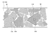
図7及び図8に示されるフォノニック結晶構造Aは多結晶構造52である。多結晶構造52では、隣接する第1ドメイン51A及び第2ドメイン51Bの界面55が、平面視において、長方形の梁13(13A)の長辺の方向に延びている。長辺の方向は、マクロな熱の伝達方向でありうる。この点以外、図7及び図8のフォノニック結晶構造Aは、図4Aのフォノニック結晶構造Aと同様の構成を有する。界面55は、平面視において、マクロな熱の伝達方向に平行にフォノニック結晶構造Aを分割している。なお、図8は、図7の領域R2の拡大図である。
The phononic crystal structure A shown in FIGS. 7 and 8 is a polycrystalline structure 52. In the polycrystalline structure 52, the interface 55 between the adjacent first domain 51A and second domain 51B extends in the direction of the long side of the rectangular beam 13 (13A) in plan view. The direction of the long side may be a macro heat transfer direction. Except for this point, the phononic crystal structure A of FIGS. 7 and 8 has the same configuration as the phononic crystal structure A of FIG. 4A. The interface 55 divides the phononic crystal structure A parallel to the macro heat transfer direction in plan view. Note that FIG. 8 is an enlarged view of the region R2 in FIG.
図4A及び図7のフォノニック結晶構造Aでは、平面視において、第1ドメイン51Aのサイズ及び第2ドメイン51Bのサイズが同一である。ただし、平面視において、フォノニック構造Aが有する第1ドメイン51A及び第2ドメイン51Bのサイズは互いに異なっていてもよい。
In the phononic crystal structure A of FIGS. 4A and 7, the size of the first domain 51A and the size of the second domain 51B are the same in plan view. However, in plan view, the sizes of the first domain 51A and the second domain 51B included in the phononic structure A may be different from each other.
図9及び図10に示されるフォノニック結晶構造Aは多結晶構造52である。多結晶構造52では、平面視において、第2ドメイン51Bが第1ドメイン51Aにより囲まれている。第1ドメイン51A及び第2ドメイン51Bの形状は、平面視において、長方形である。ただし、第1ドメイン51Aのサイズと第2ドメイン51Bのサイズとは、平面視において、異なっている。第2ドメイン51Bと、第2ドメイン51Bを囲む第1ドメイン51Aとの界面55は、平面視において、第2ドメイン51Bの外縁を構成している。これらの点以外、図9及び図10のフォノニック結晶構造Aは、図4Aのフォノニック結晶構造Aと同様の構成を有する。なお、図10は、図9の領域R3の拡大図である。
The phononic crystal structure A shown in FIGS. 9 and 10 is a polycrystalline structure 52. In the polycrystalline structure 52, the second domain 51B is surrounded by the first domain 51A in a plan view. The shapes of the first domain 51A and the second domain 51B are rectangular in plan view. However, the size of the first domain 51A and the size of the second domain 51B are different in a plan view. The interface 55 between the second domain 51B and the first domain 51A surrounding the second domain 51B constitutes the outer edge of the second domain 51B in plan view. Except for these points, the phononic crystal structure A of FIGS. 9 and 10 has the same configuration as the phononic crystal structure A of FIG. 4A. Note that FIG. 10 is an enlarged view of the region R3 in FIG.
また、図9及び図10のフォノニック結晶構造Aでは、界面55が屈曲部を有している。
Further, in the phononic crystal structure A of FIGS. 9 and 10, the interface 55 has a bent portion.
さらに、図9及び図10のフォノニック結晶構造Aは、梁13(13A)の辺に接していない第2ドメイン51Bを有する。
Furthermore, the phononic crystal structure A of FIGS. 9 and 10 has a second domain 51B that is not in contact with the side of the beam 13 (13A).
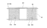
図11に示されるフォノニック結晶構造Aは、多結晶構造52である。多結晶構造52では、平面視において、第1ドメイン51Aと第2ドメイン51Bとが離間して配置されている。より具体的には、平面視において、貫通孔50を有さない領域201が、梁13(13A)の長辺方向における第1ドメイン51Aと第2ドメイン51Bとの間に設けられている。この点以外、図11のフォノニック結晶構造Aは、図4Aのフォノニック結晶構造Aと同様の構成を有する。
The phononic crystal structure A shown in FIG. 11 is a polycrystalline structure 52. In the polycrystalline structure 52, the first domain 51A and the second domain 51B are arranged apart from each other in a plan view. More specifically, in plan view, the region 201 having no through hole 50 is provided between the first domain 51A and the second domain 51B in the long side direction of the beam 13 (13A). Except for this point, the phononic crystal structure A of FIG. 11 has the same configuration as the phononic crystal structure A of FIG. 4A.
図12に示されるフォノニック結晶構造Aは、多結晶構造52である。多結晶構造52では、平面視において、第1ドメイン51Aと第2ドメイン51Bとが離間して配置されている。より具体的には、平面視において、ランダムに設けられた貫通孔50を有する領域202が、梁13(13A)の長辺方向における第1ドメイン51Aと第2ドメイン51Bとの間に設けられている。領域202では、平面視において、貫通孔50は規則的に配列していない。又は、領域202では、平面視において、規則的に配列した領域の面積が、例えば、25P2未満である。ここで、Pは、貫通孔50の配列の周期である。この点以外、図12のフォノニック結晶構造Aは、図4Aのフォノニック結晶構造Aと同様の構成を有する。
The phononic crystal structure A shown in FIG. 12 is a polycrystalline structure 52. In the polycrystalline structure 52, the first domain 51A and the second domain 51B are arranged apart from each other in a plan view. More specifically, in plan view, the region 202 having the through holes 50 randomly provided is provided between the first domain 51A and the second domain 51B in the long side direction of the beam 13 (13A). There is. In the area 202, the through holes 50 are not regularly arranged in a plan view. Alternatively, in the area 202, the area of the regularly arranged areas in the plan view is, for example, less than 25P 2 . Here, P is the cycle of the arrangement of the through holes 50. Except for this point, the phononic crystal structure A of FIG. 12 has the same configuration as the phononic crystal structure A of FIG. 4A.
図13に示されるフォノニック結晶構造Aは、多結晶構造52である。多結晶構造52は、平面視において、互いに異なった形状を有する複数のドメイン51A,51B,51C,51D,51E,51F及び51Gを含んでいる。各々のドメイン内において、複数の貫通孔50の配列の周期、及び単位格子の方位は同一である。しかし、ドメイン51Aから51G間では、単位格子の方位が各々互いに異なっている。また、平面視において、ドメイン51Aから51Gのサイズ及び形状は互いに異なっている。この形態では、これまで例示した形態に比べて、フォノニック結晶構造Aの全体で見たときに、より多くの単位格子の方位が存在する。このため、ドメイン間で単位格子の方位が異なることに基づいて熱伝導率を低下させる効果がより顕著となる。また、この形態では、ドメイン間の界面55が、平面視において、複数のランダムな方向に延びている。このため、界面抵抗に基づいて熱伝導率を低下させる効果がより顕著となる。
The phononic crystal structure A shown in FIG. 13 is a polycrystalline structure 52. The polycrystalline structure 52 includes a plurality of domains 51A, 51B, 51C, 51D, 51E, 51F and 51G having different shapes in a plan view. In each domain, the arrangement period of the plurality of through holes 50 and the orientation of the unit lattice are the same. However, the orientations of the unit lattices are different between the domains 51A to 51G. In plan view, the domains 51A to 51G have different sizes and shapes. In this form, as compared with the forms exemplified so far, when viewed as a whole of the phononic crystal structure A, there are more orientations of the unit cell. Therefore, the effect of lowering the thermal conductivity becomes more remarkable due to the difference in the orientation of the unit lattice between the domains. Further, in this mode, the interface 55 between the domains extends in a plurality of random directions in a plan view. Therefore, the effect of lowering the thermal conductivity based on the interface resistance becomes more remarkable.
また、図13のフォノニック結晶構造Aでは、隣接する第1ドメイン51Aと第2ドメイン51Bとの界面55が、平面視において、梁13(13A)の幅方向から傾いた方向に延びている。界面55は、平面視において、屈曲部も有している。
Further, in the phononic crystal structure A of FIG. 13, the interface 55 between the adjacent first domain 51A and second domain 51B extends in a direction inclined from the width direction of the beam 13 (13A) in a plan view. The interface 55 also has a bent portion in a plan view.
フォノニック結晶構造Aである多結晶構造52は、貫通孔50の配列の周期P及び/又は貫通孔50の径Dが互いに異なる第1ドメイン51A及び第2ドメイン51Bを含んでいてもよい。図14Aに示される第1ドメイン51Aにおける貫通孔50の径Dと、図14Bに示される第2ドメイン51Bにおける貫通孔50の径Dとは互いに異なっている。なお、図14Aに示される第1ドメイン51Aにおける貫通孔50の配列の周期Pと、図14Bに示される第2ドメイン51Bにおける貫通孔50の配列の周期Pとは同一である。
The polycrystalline structure 52 which is the phononic crystal structure A may include a first domain 51A and a second domain 51B in which the period P of the arrangement of the through holes 50 and/or the diameter D of the through holes 50 are different from each other. The diameter D of the through hole 50 in the first domain 51A shown in FIG. 14A and the diameter D of the through hole 50 in the second domain 51B shown in FIG. 14B are different from each other. Note that the cycle P of the arrangement of the through holes 50 in the first domain 51A shown in FIG. 14A and the cycle P of the arrangement of the through holes 50 in the second domain 51B shown in FIG. 14B are the same.
図15に示されるフォノニック結晶構造Aは、相対的に小さな周期P及び径Dを有する複数の貫通孔50が規則的に配列した第1ドメイン51Aと、相対的に大きな周期P及び径Dを有する複数の貫通孔50が規則的に配列した第2ドメイン51Bとを有する。また、図15のフォノニック結晶構造Aは、相対的に小さな周期P及び径Dを有する複数の貫通孔50を具備する領域92と、相対的に大きな周期P及び径Dを有する複数の貫通孔50を具備する領域93とを有する。領域92と領域93とは隣接している。領域92及び領域93は、それぞれ、図13の例と同様に、平面視において、互いに異なった形状を有し、かつ、単位格子の方位が各々互いに異なる複数のドメインを含んでいる。また、領域92及び領域93は、マクロな熱の伝達方向に垂直にフォノニック結晶構造Aを分割している。この形態では、第1ドメイン51Aで形成されるフォノニックバンドギャップの周波数帯域と第2ドメイン51Bで形成されるフォノニックバンドギャップの周波数帯域とが異なるため、熱伝導率の低減の効果が特に顕著となる。
The phononic crystal structure A shown in FIG. 15 has a first domain 51A in which a plurality of through holes 50 having a relatively small period P and a diameter D are regularly arranged, and a relatively large period P and a diameter D. It has the 2nd domain 51B in which a plurality of penetration holes 50 were arranged regularly. The phononic crystal structure A of FIG. 15 has a region 92 having a plurality of through holes 50 having a relatively small period P and a diameter D, and a plurality of through holes 50 having a relatively large period P and a diameter D. And a region 93 including. The area 92 and the area 93 are adjacent to each other. Similar to the example of FIG. 13, each of the regions 92 and 93 has a different shape in plan view, and includes a plurality of domains in which the orientations of the unit lattices are different from each other. Further, the region 92 and the region 93 divide the phononic crystal structure A perpendicularly to the macro heat transfer direction. In this mode, since the frequency band of the phononic band gap formed by the first domain 51A and the frequency band of the phononic band gap formed by the second domain 51B are different, the effect of reducing the thermal conductivity is particularly remarkable. Becomes
図16に示されるフォノニック結晶構造Aでは、相対的に小さな周期P及び径Dを有する複数の貫通孔50が規則的に配列した第1ドメイン51Aと、相対的に大きな周期P及び径Dを有する複数の貫通孔50が規則的に配列した第2ドメイン51Bとを含む。図16のフォノニック結晶構造Aは、平面視において、互いに異なった形状を有し、かつ、単位格子の方位が各々互いに異なる複数のドメインを含んでいる。この形態では、第1ドメイン51Aで形成されるフォノニックバンドギャップの周波数帯域と第2ドメイン51Bで形成されるフォノニックバンドギャップの周波数帯域とが異なるため、熱伝導率の低減の効果が特に顕著となる。
In the phononic crystal structure A shown in FIG. 16, a first domain 51A in which a plurality of through holes 50 having a relatively small period P and a diameter D are regularly arranged, and a relatively large period P and a diameter D are provided. The second domain 51B in which the plurality of through holes 50 are regularly arranged is included. The phononic crystal structure A shown in FIG. 16 includes a plurality of domains having different shapes in a plan view and having unit cell orientations different from each other. In this mode, since the frequency band of the phononic band gap formed by the first domain 51A and the frequency band of the phononic band gap formed by the second domain 51B are different, the effect of reducing the thermal conductivity is particularly remarkable. Becomes
貫通孔50の配列の周期Pは、例えば、1nm以上300nm以下である。これは、熱を運ぶフォノンの波長が、主として、1nmから300nmの範囲に及ぶためである。周期Pは、平面視において隣接する貫通孔50間の中心間距離により定められる(図14A,14B参照)。
The cycle P of the arrangement of the through holes 50 is, for example, 1 nm or more and 300 nm or less. This is because the wavelengths of phonons that carry heat range primarily from 1 nm to 300 nm. The period P is determined by the center-to-center distance between adjacent through holes 50 in plan view (see FIGS. 14A and 14B).
貫通孔50の径Dは、周期Pに対する比D/Pにより表して、例えば、D/P≧0.5である。比D/P<0.5である場合、梁13(13A,13B)における空隙率が過度に低下して、熱伝導率が十分に低下しないことがある。比D/Pの上限は、隣接する貫通孔50同士が接しないために、例えば、0.9未満である。径Dは、貫通孔50の開口の径である。貫通孔50の開口の形状が平面視において円である場合、径Dは当該円の直径である。貫通孔50の開口の形状は平面視において円でなくてもよい。この場合、径Dは、開口の面積と同じ面積を有する仮想の円の直径により定められる(図14A,14B参照)。
The diameter D of the through hole 50 is represented by the ratio D/P to the period P, and for example, D/P≧0.5. When the ratio D/P<0.5, the porosity of the beam 13 (13A, 13B) may be excessively reduced, and the thermal conductivity may not be sufficiently reduced. The upper limit of the ratio D/P is, for example, less than 0.9 because adjacent through holes 50 do not contact each other. The diameter D is the diameter of the opening of the through hole 50. When the shape of the opening of the through hole 50 is a circle in plan view, the diameter D is the diameter of the circle. The shape of the opening of the through hole 50 may not be a circle in plan view. In this case, the diameter D is defined by the diameter of a virtual circle having the same area as the opening (see FIGS. 14A and 14B).
規則的に配列した複数の貫通孔50を具備する単位格子91の種類は、例えば、正方格子(図17A)、六方格子(図17B)、長方格子(図17C)、及び面心長方格子(図17D)である。ただし、単位格子91の種類は、これらの例に限定されない。
The type of the unit lattice 91 having the plurality of through holes 50 arranged regularly includes, for example, a square lattice (FIG. 17A), a hexagonal lattice (FIG. 17B), a rectangular lattice (FIG. 17C), and a face-centered rectangular lattice. (FIG. 17D). However, the type of the unit lattice 91 is not limited to these examples.
第1梁13A及び/又は第2梁13Bが有しうるフォノニック結晶構造Aは、上述した構造に限定されない。フォノニック結晶構造Aは、例えば、特開2017-223644号公報に開示の構造であってもよい。ただし、図4A及び図4Bをはじめとして上述した各図に示される、単位格子の方位が互いに異なる2以上のフォノニック結晶領域を有するフォノニック結晶構造Aでは、梁13の熱伝導率のさらなる低減、即ち、断熱性のさらなる向上、が可能となる。これは、以下の理由による。
The phononic crystal structure A that the first beam 13A and/or the second beam 13B may have is not limited to the above structure. The phononic crystal structure A may be, for example, the structure disclosed in JP-A-2017-223644. However, in the phononic crystal structure A having two or more phononic crystal regions having unit cell orientations different from each other as shown in each of the above-described drawings including FIG. 4A and FIG. 4B, the thermal conductivity of the beam 13 is further reduced, that is, It is possible to further improve the heat insulating property. This is for the following reason.
本発明者らの検討によれば、フォノニック結晶構造によってもたらされる熱伝導率の低減の程度は、熱の伝達方向と、フォノニック結晶構造の単位格子の方位(orientation)とが成す角度に依存する。これは、PBGの帯域広さ、PBGの数、及びフォノンの平均群速度といった熱伝導に関わる要素が、当該角度に依存するためと考えられる。また、熱の伝達に関して、マクロ的には高温から低温の方向にフォノンは流れる。一方、ナノメートルのオーダーにあるミクロ領域に着目すると、フォノンの流れる方向には指向性がみられない。即ち、ミクロ的にはフォノンの流れる方向は一様ではない。単位格子の方位が一様に揃った複数のフォノニック結晶領域を有するフォノニック結晶構造Aでは、ミクロで見て、ある特定の方向に流れるフォノンに対しては相互作用が最大となるものの、それ以外の方向に流れるフォノンに対しては相互作用が弱まる。一方、単位格子の方位が互いに異なる2以上のフォノニック結晶領域を有するフォノニック結晶構造Aでは、ミクロで見て、複数の方向に流れる各フォノンに対する相互作用を高めることができる。これにより、梁13の熱伝導率のさらなる低減が可能となる。
According to the study by the present inventors, the degree of reduction in thermal conductivity brought about by the phononic crystal structure depends on the angle formed by the heat transfer direction and the orientation of the unit cell of the phononic crystal structure. It is considered that this is because the factors related to heat conduction such as the PBG band width, the number of PBGs, and the average group velocity of phonons depend on the angle. In terms of heat transfer, phonons flow macroscopically from high temperature to low temperature. On the other hand, focusing on the micro region on the order of nanometers, there is no directivity in the direction of phonon flow. That is, the direction of phonon flow is not uniform microscopically. In the phononic crystal structure A having a plurality of phononic crystal regions in which the unit cell orientations are uniformly aligned, the interaction is maximum with respect to phonons flowing in a specific direction in a microscopic view. The interaction weakens for phonons flowing in the direction. On the other hand, in the phononic crystal structure A having two or more phononic crystal regions in which the unit cell orientations are different from each other, the interaction with each phonon flowing in a plurality of directions can be enhanced when viewed microscopically. Thereby, the thermal conductivity of the beam 13 can be further reduced.
(実施形態2)
実施形態2の赤外線センサが図18A及び図18Bに示される。図18Aには、図18Bの赤外線センサ1Bの断面18A-18Aが示される。赤外線センサ1Bは、熱型赤外線センサの1種であるボロメータ型赤外線センサである。 (Embodiment 2)
The infrared sensor of Embodiment 2 is shown in FIGS. 18A and 18B. FIG. 18A shows across section 18A-18A of the infrared sensor 1B of FIG. 18B. The infrared sensor 1B is a bolometer-type infrared sensor, which is a type of thermal infrared sensor.
実施形態2の赤外線センサが図18A及び図18Bに示される。図18Aには、図18Bの赤外線センサ1Bの断面18A-18Aが示される。赤外線センサ1Bは、熱型赤外線センサの1種であるボロメータ型赤外線センサである。 (Embodiment 2)
The infrared sensor of Embodiment 2 is shown in FIGS. 18A and 18B. FIG. 18A shows a
赤外線センサ1Bは、ベース基板11の上に絶縁層26をさらに備える。断面視において、絶縁層26は、ベース基板11の上面14と、第1梁13A及び第2梁13B(半導体層21)との間に配置されている。平面視において、絶縁層26は、赤外線受光部12及び赤外線反射膜23を囲むように配置されている。また、第1支柱15Aにおける信号読み出し端子22Aと第1梁13Aとの間の区間は、絶縁層26により囲まれている。第2支柱15Bにおける信号読み出し端子22Bと第2梁13Bとの間の区間は、絶縁層26により囲まれている。
The infrared sensor 1B further includes an insulating layer 26 on the base substrate 11. In a cross-sectional view, the insulating layer 26 is arranged between the upper surface 14 of the base substrate 11 and the first beam 13A and the second beam 13B (semiconductor layer 21). In a plan view, the insulating layer 26 is arranged so as to surround the infrared light receiving portion 12 and the infrared reflective film 23. The section between the signal read terminal 22A and the first beam 13A in the first support column 15A is surrounded by the insulating layer 26. The section between the signal read terminal 22B and the second beam 13B in the second support column 15B is surrounded by the insulating layer 26.
絶縁層26を構成する材料は、例えば、SiO2等の酸化物である。ただし、絶縁層26を構成する材料は、上記例に限定されない。
The material forming the insulating layer 26 is, for example, an oxide such as SiO 2 . However, the material forming the insulating layer 26 is not limited to the above example.
実施形態2の赤外線センサ1Bにおけるその他の構成は、好ましい形態を含め、実施形態1の赤外線センサ1Aにおける対応する構成と同様である。また、実施形態2の赤外線センサ1Bの作動原理は、実施形態1の赤外線センサ1Aの作動原理と同じである。
The other configurations of the infrared sensor 1B of the second embodiment are the same as the corresponding configurations of the infrared sensor 1A of the first embodiment, including a preferable mode. The operating principle of the infrared sensor 1B of the second embodiment is the same as the operating principle of the infrared sensor 1A of the first embodiment.
(実施形態3)
実施形態3の赤外線センサが図19に示される。図19に示される赤外線センサ1Cは、熱型赤外線センサの1種であるボロメータ型赤外線センサである。赤外線センサ1Cは、ベース基板11、ボロメータ赤外線受光部12、第1梁13A、第2梁13B、第1配線20A、第2配線20B、及び赤外線反射膜23を備える。第1梁13A及び第2梁13Bは、それぞれ、ベース基板11と接続された接続部16A,16Bを有する。第1梁13A及び第2梁13Bの各々は、ベース基板11から離間した離間部17を有する。第1梁13A及び第2梁13Bは、それぞれ、一方の端部に接続部16A,16Bを有している。第1梁13A及び第2梁13Bの各々は、離間部17において赤外線受光部12と物理的に接合されている。赤外線受光部12と物理的に接合されている位置は、第1梁13A及び第2梁13Bの各々における他方の端部である。赤外線受光部12は、第1梁13A及び第2梁13Bによって、ベース基板11とは離間した状態で支持されている。この離間は、ベース基板11と赤外線受光部12との熱的な絶縁を高めている。 (Embodiment 3)
The infrared sensor of the third embodiment is shown in FIG. Theinfrared sensor 1C shown in FIG. 19 is a bolometer-type infrared sensor which is a type of thermal infrared sensor. The infrared sensor 1C includes a base substrate 11, a bolometer infrared light receiver 12, a first beam 13A, a second beam 13B, a first wiring 20A, a second wiring 20B, and an infrared reflecting film 23. The first beam 13A and the second beam 13B respectively have connecting portions 16A and 16B connected to the base substrate 11. Each of the first beam 13</b>A and the second beam 13</b>B has a separating portion 17 that is separated from the base substrate 11. The first beam 13A and the second beam 13B each have connecting portions 16A and 16B at one end. Each of the first beam 13</b>A and the second beam 13</b>B is physically joined to the infrared light receiving section 12 at the spacing section 17. The position that is physically joined to the infrared light receiving unit 12 is the other end of each of the first beam 13A and the second beam 13B. The infrared light receiving portion 12 is supported by the first beam 13A and the second beam 13B while being separated from the base substrate 11. This separation enhances thermal insulation between the base substrate 11 and the infrared light receiving portion 12.
実施形態3の赤外線センサが図19に示される。図19に示される赤外線センサ1Cは、熱型赤外線センサの1種であるボロメータ型赤外線センサである。赤外線センサ1Cは、ベース基板11、ボロメータ赤外線受光部12、第1梁13A、第2梁13B、第1配線20A、第2配線20B、及び赤外線反射膜23を備える。第1梁13A及び第2梁13Bは、それぞれ、ベース基板11と接続された接続部16A,16Bを有する。第1梁13A及び第2梁13Bの各々は、ベース基板11から離間した離間部17を有する。第1梁13A及び第2梁13Bは、それぞれ、一方の端部に接続部16A,16Bを有している。第1梁13A及び第2梁13Bの各々は、離間部17において赤外線受光部12と物理的に接合されている。赤外線受光部12と物理的に接合されている位置は、第1梁13A及び第2梁13Bの各々における他方の端部である。赤外線受光部12は、第1梁13A及び第2梁13Bによって、ベース基板11とは離間した状態で支持されている。この離間は、ベース基板11と赤外線受光部12との熱的な絶縁を高めている。 (Embodiment 3)
The infrared sensor of the third embodiment is shown in FIG. The
ベース基板11は、赤外線受光部12が設けられた上面14に凹部27を有する。平面視において、赤外線受光部12の面積に比べて凹部27の面積は大きい。また、平面視において、赤外線受光部12は、凹部27の外縁に囲まれている。凹部27は、赤外線受光部12、並びに第1梁13Aの離間部17及び第2梁13Bの離間部17と、ベース基板11との間に位置している。第1梁13Aは、接続部16Aにおいてベース基板11と物理的に接続されている。第2梁13Bは、接続部16Bにおいてベース基板11と物理的に接続されている。断面視において、赤外線受光部12、並びに第1梁13Aの離間部16A及び第2梁13Bの離間部16Bは、ベース基板11の凹部27上に懸架されている。この懸架により、ベース基板11と赤外線受光部12との熱的な絶縁が高められる。
The base substrate 11 has a concave portion 27 on the upper surface 14 on which the infrared light receiving portion 12 is provided. In plan view, the area of the recess 27 is larger than the area of the infrared light receiving portion 12. Further, the infrared light receiving portion 12 is surrounded by the outer edge of the recess 27 in a plan view. The recess 27 is located between the infrared light receiving portion 12, the spacing portion 17 of the first beam 13A and the spacing portion 17 of the second beam 13B, and the base substrate 11. The first beam 13A is physically connected to the base substrate 11 at the connecting portion 16A. The second beam 13B is physically connected to the base substrate 11 at the connecting portion 16B. In the cross-sectional view, the infrared light receiving portion 12, the spacing portion 16A of the first beam 13A and the spacing portion 16B of the second beam 13B are suspended on the recess 27 of the base substrate 11. Due to this suspension, the thermal insulation between the base substrate 11 and the infrared light receiving portion 12 is enhanced.
赤外線センサ1Cでは、抵抗変化膜33の抵抗の読み取りが実施される。読み取りのために、図19に示される赤外線センサ1Cは、ベース基板11の内部にROIC(図示せず)をさらに備えている。第1配線20Aの端部とROICとは電気的に接続されている。第2配線20Bの端部とROICとは電気的に接続されている。抵抗変化膜33の抵抗は、下部電極31、上部電極32、第1配線20A、及び第2配線20Bを介して読み取り可能である。赤外線センサ1Cは、抵抗変化膜33の抵抗を読み取るためのさらなる部材を備えていてもよい。
In the infrared sensor 1C, the resistance of the resistance change film 33 is read. For reading, the infrared sensor 1C shown in FIG. 19 further includes a ROIC (not shown) inside the base substrate 11. The end of the first wiring 20A and the ROIC are electrically connected. The end of the second wiring 20B and the ROIC are electrically connected. The resistance of the resistance change film 33 can be read through the lower electrode 31, the upper electrode 32, the first wiring 20A, and the second wiring 20B. The infrared sensor 1C may include a further member for reading the resistance of the resistance change film 33.
赤外線受光部12に赤外線が入射すると、赤外線受光部12の温度が上昇する。このとき、赤外線受光部12の温度は、熱浴であるベース基板11から熱的に絶縁されているほど、大きく上昇する。ボロメータ赤外線受光部12を備える赤外線センサ1Cでは、温度上昇に伴って、抵抗変化膜33の抵抗が変化する。変化した抵抗に対応する電気的な信号をROICで処理して赤外線が検知される。処理によっては、赤外線センサ1Cによる赤外線の強度測定、及び/又は対象物の温度測定が可能である。ただし、上述のように、本開示の赤外線センサにおいて、赤外線受光部12に含まれる抵抗変化膜33の抵抗の読み取りは、ベース基板11の内部に設けられたROICによる態様に限定されない。
When the infrared ray is incident on the infrared ray receiving section 12, the temperature of the infrared ray receiving section 12 rises. At this time, the temperature of the infrared light receiving portion 12 increases as it is thermally insulated from the base substrate 11 which is a heat bath. In the infrared sensor 1C including the bolometer infrared light receiving unit 12, the resistance of the resistance change film 33 changes as the temperature rises. The infrared signal is detected by processing the electrical signal corresponding to the changed resistance with the ROIC. Depending on the processing, the infrared intensity can be measured by the infrared sensor 1C and/or the temperature of the object can be measured. However, as described above, in the infrared sensor of the present disclosure, the reading of the resistance of the resistance change film 33 included in the infrared light receiving unit 12 is not limited to the mode by the ROIC provided inside the base substrate 11.
実施形態1の赤外線センサ1Aと実施形態3の赤外線センサ1Cとは、ベース基板11の上面14に対する赤外線受光部12、第1梁13A、及び第2梁13Bの懸架の方式が異なる。また、実施形態3の赤外線センサ1Cでは、赤外線反射膜23が凹部27の底面に配置されている。ただし、ベース基板11の表面における赤外線受光部12に対面する位置に赤外線反射膜23が配置されている点において、赤外線センサ1Cの構成は赤外線センサ1Aの構成と同じである。実施形態3の赤外線センサ1Cにおけるその他の構成は、好ましい形態を含め、実施形態1の赤外線センサ1Aにおける対応する構成と同様である。
The infrared sensor 1A of the first embodiment and the infrared sensor 1C of the third embodiment are different in the suspension method of the infrared light receiving portion 12, the first beam 13A, and the second beam 13B with respect to the upper surface 14 of the base substrate 11. Further, in the infrared sensor 1C of the third embodiment, the infrared reflection film 23 is arranged on the bottom surface of the recess 27. However, the configuration of the infrared sensor 1C is the same as the configuration of the infrared sensor 1A in that the infrared reflection film 23 is arranged on the surface of the base substrate 11 at a position facing the infrared light receiving portion 12. The rest of the configuration of the infrared sensor 1C of the third embodiment is the same as the corresponding configuration of the infrared sensor 1A of the first embodiment, including the preferred form.
本開示の赤外線センサは、本発明の効果が得られる限り、上述した以外の任意の部材を有していてもよい。
The infrared sensor of the present disclosure may have any member other than those described above as long as the effects of the present invention can be obtained.
[赤外線センサアレイ]
実施形態1~3の赤外線センサ1A~1Cは、原理上、単独で赤外線センサとして機能する。個々の赤外線センサを一画素として、複数の赤外線センサをベース基板11上にアレイ状に配列させてもよい。配列は、典型的には、二次元アレイ状である。複数の赤外線センサが配列したアレイ構造により、例えば、有限の温度を有する物体のイメージング、及び/又は赤外線放射、若しくはレーザー光線の強度分布の評価が可能となる。なお、アレイ状に配列される複数の赤外線センサの少なくとも一部が、本開示の赤外線センサであればよい。アレイ状に配列される複数の赤外線センサの全部が、本開示の赤外線センサであってもよい。本開示には、赤外線センサアレイであって、二次元アレイ状に配置された複数の赤外線センサを具備し、当該複数の赤外線センサが本開示の赤外線センサを含むセンサアレイが含まれる。 [Infrared sensor array]
Theinfrared sensors 1A to 1C of the first to third embodiments function independently as infrared sensors in principle. A plurality of infrared sensors may be arranged in an array on the base substrate 11 with each infrared sensor as one pixel. The array is typically a two-dimensional array. The array structure in which a plurality of infrared sensors are arranged enables, for example, imaging of an object having a finite temperature and/or evaluation of infrared radiation or intensity distribution of a laser beam. At least a part of the plurality of infrared sensors arranged in an array may be the infrared sensor of the present disclosure. All of the plurality of infrared sensors arranged in an array may be the infrared sensor of the present disclosure. The present disclosure includes an infrared sensor array including a plurality of infrared sensors arranged in a two-dimensional array, the plurality of infrared sensors including the infrared sensor of the present disclosure.
実施形態1~3の赤外線センサ1A~1Cは、原理上、単独で赤外線センサとして機能する。個々の赤外線センサを一画素として、複数の赤外線センサをベース基板11上にアレイ状に配列させてもよい。配列は、典型的には、二次元アレイ状である。複数の赤外線センサが配列したアレイ構造により、例えば、有限の温度を有する物体のイメージング、及び/又は赤外線放射、若しくはレーザー光線の強度分布の評価が可能となる。なお、アレイ状に配列される複数の赤外線センサの少なくとも一部が、本開示の赤外線センサであればよい。アレイ状に配列される複数の赤外線センサの全部が、本開示の赤外線センサであってもよい。本開示には、赤外線センサアレイであって、二次元アレイ状に配置された複数の赤外線センサを具備し、当該複数の赤外線センサが本開示の赤外線センサを含むセンサアレイが含まれる。 [Infrared sensor array]
The
[赤外線センサの製造方法]
本開示の赤外線センサは、化学気相成長(CVD)、スパッタリング、及び蒸着等の各種の薄膜形成手法;並びに、電子線リソグラフィー、フォトリソグラフィー、ブロック共重合体リソグラフィー、及び選択的エッチング等の各種の微細加工手法及びパターン形成手法;の組み合わせによる製造が可能である。ブロック共重合体リソグラフィーは、フォノニック結晶構造Aの形成に適している。 [Infrared sensor manufacturing method]
The infrared sensor of the present disclosure is applicable to various thin film forming methods such as chemical vapor deposition (CVD), sputtering, and vapor deposition; and various kinds of electron beam lithography, photolithography, block copolymer lithography, and selective etching. It is possible to manufacture by a combination of a fine processing method and a pattern forming method. Block copolymer lithography is suitable for forming the phononic crystal structure A.
本開示の赤外線センサを製造する方法の一例が、図20A~図22Oの参照により、以下に説明される。以下の方法により製造する赤外線センサは、実施形態1の赤外線センサ1Aである。ただし、以下の方法により製造する赤外線センサ1Aは、第1梁13A及び第2梁13Bがフォノニック結晶構造Aを有している。本開示の赤外線センサを製造する方法は、以下の例に限定されない。
An example of a method of manufacturing the infrared sensor of the present disclosure will be described below with reference to FIGS. 20A to 22O. The infrared sensor manufactured by the following method is the infrared sensor 1A of the first embodiment. However, in the infrared sensor 1A manufactured by the following method, the first beam 13A and the second beam 13B have the phononic crystal structure A. The method for manufacturing the infrared sensor of the present disclosure is not limited to the following examples.
図20A:ベース基板11が準備される。次に。ベース基板11の上面14に金属層が形成される。金属層は、例えば、Cr層である。金属層は、例えば、スパッタリングにより形成される。金属層の厚さは、例えば200nmである。形成された金属層の上にフォトレジスト101が形成される。フォトレジスト101を用いたフォトリソグラフィー及び選択的エッチングによって金属層が微細加工されて、赤外線反射膜23、第1読み出し端子22A、及び第2読み出し端子22Bを形成する。
FIG. 20A: The base substrate 11 is prepared. next. A metal layer is formed on the upper surface 14 of the base substrate 11. The metal layer is, for example, a Cr layer. The metal layer is formed by sputtering, for example. The thickness of the metal layer is, for example, 200 nm. A photoresist 101 is formed on the formed metal layer. The metal layer is finely processed by photolithography and selective etching using the photoresist 101 to form the infrared reflection film 23, the first read terminal 22A, and the second read terminal 22B.
図20B:フォトレジスト101が除去される。赤外線反射膜23、第1読み出し端子22A、及び第2読み出し端子22Bを覆うように犠牲層102が形成される。犠牲層102は、例えば、SiO2層である。犠牲層102は、例えば、CVDにより形成される。犠牲層102の厚さは、例えば、1~4μmである。犠牲層102の厚さは、この方法により製造する赤外線センサ1Aにおける赤外線受光部12とベース基板11との離間距離に相当する。離間距離は、より具体的には、ベース基板11の上面14と受光部支持膜18の下面との間の距離である。
FIG. 20B: The photoresist 101 is removed. The sacrificial layer 102 is formed so as to cover the infrared reflective film 23, the first read terminal 22A, and the second read terminal 22B. The sacrificial layer 102 is, for example, a SiO 2 layer. The sacrificial layer 102 is formed by, for example, CVD. The thickness of the sacrificial layer 102 is, for example, 1 to 4 μm. The thickness of the sacrificial layer 102 corresponds to the distance between the infrared light receiving portion 12 and the base substrate 11 in the infrared sensor 1A manufactured by this method. The separation distance is, more specifically, a distance between the upper surface 14 of the base substrate 11 and the lower surface of the light receiving unit support film 18.
図20C:犠牲層102の上に、半導体層103が形成される。半導体層103は、例えば、SiN層である。半導体層103は、例えば、CVDにより形成される。半導体層103の厚さは、例えば、100nmである。半導体層103は、後の微細加工及びパターン形成により、第1梁13A、第2梁13B、及び受光部支持膜18となる。
20C: The semiconductor layer 103 is formed on the sacrificial layer 102. The semiconductor layer 103 is, for example, a SiN layer. The semiconductor layer 103 is formed by, for example, CVD. The semiconductor layer 103 has a thickness of 100 nm, for example. The semiconductor layer 103 becomes the first beam 13A, the second beam 13B, and the light-receiving portion support film 18 by the subsequent fine processing and pattern formation.
図20D:半導体層103の上に、ハードマスク104が形成される。ハードマスク104は、例えば、SiO2層である。ハードマスク104は、例えば、CVDにより形成される。ハードマスク104の厚さは、例えば、30nmである。ハードマスク104は、半導体層103に対するフォノニック結晶構造Aの形成に使用される。
FIG. 20D: A hard mask 104 is formed on the semiconductor layer 103. The hard mask 104 is, for example, a SiO 2 layer. The hard mask 104 is formed by, for example, CVD. The thickness of the hard mask 104 is, for example, 30 nm. The hard mask 104 is used to form the phononic crystal structure A on the semiconductor layer 103.
図20E:ハードマスク104の上に、フォトレジスト105が形成される。フォトリソグラフィーにより、半導体層103におけるフォノニック結晶構造Aを形成すべき領域と平面視において一致するハードマスク104の領域が露出される。次に、ハードマスク104における露出された領域に対して、ブロック共重合体の自己組織化膜106が形成される。自己組織化膜106は、フォノニック結晶構造Aを形成するためのブロック共重合体リソグラフィーに使用される。
FIG. 20E: A photoresist 105 is formed on the hard mask 104. By photolithography, a region of the hard mask 104 that is identical to a region of the semiconductor layer 103 where the phononic crystal structure A is to be formed in plan view is exposed. Next, a block copolymer self-assembled film 106 is formed on the exposed region of the hard mask 104. The self-assembled film 106 is used in block copolymer lithography for forming the phononic crystal structure A.
図20F:ブロック共重合体リソグラフィーにより、規則的に配列した複数の貫通孔107がハードマスク104に形成される。自己組織化膜106及びフォトレジスト105が除去される。
FIG. 20F: A plurality of regularly arranged through holes 107 are formed in the hard mask 104 by block copolymer lithography. The self-assembled film 106 and the photoresist 105 are removed.
図20G:フォトリソグラフィーにより半導体層103を微細加工及びパターン形成して、第1梁13A、第2梁13B、及び受光部支持膜18が形成される。第1梁13A、第2梁13B、及び受光部支持膜18は、単層の半導体層21を構成する。
FIG. 20G: The semiconductor layer 103 is finely processed and patterned by photolithography to form the first beam 13A, the second beam 13B, and the light receiving portion support film 18. The first beam 13A, the second beam 13B, and the light receiving portion support film 18 form a single-layer semiconductor layer 21.
図20H:ハードマスク104をレジストとする選択的エッチングによって、第1梁13A及び第2梁13Bに対して、平面視したときに、複数の貫通孔107に対応する位置に規則的に配列した複数の貫通孔50が形成される。形成された複数の貫通孔50は、フォノニック結晶構造Aを構成する。
FIG. 20H: A plurality of the first beams 13A and the second beams 13B which are regularly arrayed at positions corresponding to the plurality of through holes 107 in a plan view by selective etching using the hard mask 104 as a resist. Through holes 50 are formed. The plurality of formed through holes 50 form a phononic crystal structure A.
図20I:ハードマスク104が除去される。
FIG. 20I: The hard mask 104 is removed.
図20J:第1梁13A、第2梁13B、及び受光部支持膜18の上に、第1配線20A、第2配線20B、及び下部電極31を形成する。第1配線20A、第2配線20B、及び下部電極31は、例えば、TiNにより構成される。第1配線20A、第2配線20B、及び下部電極31は、例えば、スパッタリングにより形成される。これらの部材の厚さは、例えば、8nmである。
20J: First wiring 20A, second wiring 20B, and lower electrode 31 are formed on first beam 13A, second beam 13B, and light-receiving portion support film 18. The first wiring 20A, the second wiring 20B, and the lower electrode 31 are made of, for example, TiN. The first wiring 20A, the second wiring 20B, and the lower electrode 31 are formed by sputtering, for example. The thickness of these members is, for example, 8 nm.
図20K:下部電極31の上に、抵抗変化膜33が形成される。抵抗変化膜33は、例えば、非晶質のSiにより構成される。抵抗変化膜33は、例えば、CVDにより形成される。抵抗変化膜33の厚さは、例えば、100nmである。
20K: The resistance change film 33 is formed on the lower electrode 31. The resistance change film 33 is made of, for example, amorphous Si. The resistance change film 33 is formed by, for example, CVD. The resistance change film 33 has a thickness of, for example, 100 nm.
図20L:抵抗変化膜33の上に、第2配線20Bと接続されるように、上部電極32が形成される。上部電極32は、例えば、TiNにより構成される。上部電極32は、例えば、スパッタリングにより形成される。上部電極32の厚さは、例えば、8nmである。
20L: An upper electrode 32 is formed on the resistance change film 33 so as to be connected to the second wiring 20B. The upper electrode 32 is made of, for example, TiN. The upper electrode 32 is formed by sputtering, for example. The thickness of the upper electrode 32 is, for example, 8 nm.
図20M:選択的エッチングにより、第1配線20A、第2配線20B、第1梁13A、第2梁13B、及び犠牲層102にコンタクトホール108が形成され、第1読み出し端子22A及び第2読み出し端子22Bを露出させる。
FIG. 20M: Contact holes 108 are formed in the first wiring 20A, the second wiring 20B, the first beam 13A, the second beam 13B, and the sacrificial layer 102 by selective etching, and the first read terminal 22A and the second read terminal are formed. 22B is exposed.
図20N:形成されたコンタクトホール108に金属が堆積されて、第1支柱15A及び第2支柱15Bを形成する。堆積される金属は、例えば、Alである。第1支柱15A及び第2支柱15Bは、例えば、スパッタリングにより形成される。
FIG. 20N: Metal is deposited in the formed contact holes 108 to form the first support columns 15A and the second support columns 15B. The metal deposited is, for example, Al. The first support 15A and the second support 15B are formed by, for example, sputtering.
図20O:犠牲層102が、例えば、気相フッ化水素(HF)エッチングにより除去される。このようにして、本開示の赤外線センサの1形態である赤外線センサ1Aが製造される。なお、犠牲層102をパターンエッチングすることにより、絶縁層26が形成可能である。
FIG. 20O: The sacrificial layer 102 is removed by, for example, vapor phase hydrogen fluoride (HF) etching. In this way, the infrared sensor 1A which is one form of the infrared sensor of the present disclosure is manufactured. The insulating layer 26 can be formed by pattern-etching the sacrificial layer 102.
本開示の赤外線センサは、従来の赤外線センサの用途を含む種々の用途に使用できる。
The infrared sensor of the present disclosure can be used in various applications including the applications of conventional infrared sensors.
1A,1B,1C 赤外線センサ
11 ベース基板
12 (ボロメータ)赤外線受光部
13A 第1梁
13B 第2梁
14 上面
15A 第1支柱
15B 第2支柱
16A (第1梁の)接続部
16B (第2梁の)接続部
17 離間部
18 受光部支持膜
20A 第1配線
20B 第2配線
21 半導体層
22A 第1読み出し端子
22B 第2読み出し端子
23 赤外線反射膜
25 絶縁層
27 凹部
31 下部電極
32 上部電極
33 抵抗変化膜
34,34A,34B 帯状部
35 バスライン
36 接続ライン
50 貫通孔
51A 第1ドメイン
51B 第2ドメイン
52 フォノニック多結晶構造
53A,53B 方位
55 界面
31A 第1の支柱
31B 第2の支柱
91,91A,91B 単位格子
92 領域
93 領域
101 フォトレジスト
102 犠牲層
103 半導体層
104 ハードマスク
105 フォトレジスト
106 自己組織化膜
107 貫通孔
108 コンタクトホール 1A, 1B,1C Infrared sensor 11 Base substrate 12 (bolometer) Infrared light receiving part 13A 1st beam 13B 2nd beam 14 Upper surface 15A 1st support|pillar 15B 2nd support|pillar 16A (of 1st beam) connection part 16B (of 2nd beam) ) Connection portion 17 Separation portion 18 Light receiving portion support film 20A First wiring 20B Second wiring 21 Semiconductor layer 22A First readout terminal 22B Second readout terminal 23 Infrared reflection film 25 Insulation layer 27 Recess 31 Lower electrode 32 Upper electrode 33 Resistance change Membrane 34, 34A, 34B Strip portion 35 Bus line 36 Connection line 50 Through hole 51A First domain 51B Second domain 52 Phononic polycrystal structure 53A, 53B Orientation 55 Interface 31A First pillar 31B Second pillar 91, 91A, 91B Unit Lattice 92 Region 93 Region 101 Photoresist 102 Sacrificial Layer 103 Semiconductor Layer 104 Hard Mask 105 Photoresist 106 Self-Assembled Film 107 Through Hole 108 Contact Hole
11 ベース基板
12 (ボロメータ)赤外線受光部
13A 第1梁
13B 第2梁
14 上面
15A 第1支柱
15B 第2支柱
16A (第1梁の)接続部
16B (第2梁の)接続部
17 離間部
18 受光部支持膜
20A 第1配線
20B 第2配線
21 半導体層
22A 第1読み出し端子
22B 第2読み出し端子
23 赤外線反射膜
25 絶縁層
27 凹部
31 下部電極
32 上部電極
33 抵抗変化膜
34,34A,34B 帯状部
35 バスライン
36 接続ライン
50 貫通孔
51A 第1ドメイン
51B 第2ドメイン
52 フォノニック多結晶構造
53A,53B 方位
55 界面
31A 第1の支柱
31B 第2の支柱
91,91A,91B 単位格子
92 領域
93 領域
101 フォトレジスト
102 犠牲層
103 半導体層
104 ハードマスク
105 フォトレジスト
106 自己組織化膜
107 貫通孔
108 コンタクトホール 1A, 1B,
Claims (16)
- 赤外線センサであって、
ベース基板;
ボロメータ赤外線受光部;
第1梁;
第2梁;
第1配線;
第2配線;及び
赤外線反射膜;
を具備し、
ここで、
前記第1梁及び前記第2梁の各々は、前記ベース基板、及び/又は前記ベース基板上の部材と接続された接続部と、前記ベース基板から離間した離間部と、を有し、かつ、前記離間部において前記赤外線受光部と物理的に接合され、
前記赤外線受光部は、前記第1梁及び前記第2梁によって、前記ベース基板とは離間した状態で支持されており、
前記赤外線受光部は、下部電極と、上部電極と、温度によって電気抵抗が変化する抵抗変化材料から構成される抵抗変化膜と、を含み、
前記抵抗変化膜は、前記下部電極及び前記上部電極によって厚さ方向に挟持され、
前記下部電極及び前記上部電極の各々は、前記抵抗変化膜と電気的に接続され、
前記下部電極及び前記上部電極は、前記第1配線及び前記第2配線と、それぞれ電気的に接続され、
前記下部電極及び前記上部電極から選ばれる少なくとも1つの電極が、ラインアンドスペース構造を有し、
前記赤外線反射膜は、前記ベース基板の表面における前記赤外線受光部に対面する位置に設けられている、
赤外線センサ。 An infrared sensor,
Base substrate;
Bolometer infrared receiver;
First beam;
Second beam;
First wiring;
Second wiring; and infrared reflection film;
Equipped with,
here,
Each of the first beam and the second beam has a connecting portion connected to the base substrate and/or a member on the base substrate, and a spacing portion spaced from the base substrate, and Physically joined to the infrared light receiving portion in the separated portion,
The infrared light receiving unit is supported by the first beam and the second beam in a state of being separated from the base substrate,
The infrared light receiving unit includes a lower electrode, an upper electrode, and a resistance change film made of a resistance change material whose electric resistance changes with temperature,
The resistance change film is sandwiched in the thickness direction by the lower electrode and the upper electrode,
Each of the lower electrode and the upper electrode is electrically connected to the resistance change film,
The lower electrode and the upper electrode are electrically connected to the first wiring and the second wiring, respectively.
At least one electrode selected from the lower electrode and the upper electrode has a line and space structure,
The infrared reflective film is provided at a position facing the infrared light receiving portion on the surface of the base substrate,
Infrared sensor. - 請求項1に記載の赤外線センサであって、
前記下部電極は、第1の前記ラインアンドスペース構造を有し、
前記上部電極は、第2の前記ラインアンドスペース構造を有し、
平面視において、前記第1のラインアンドスペース構造の整列方向と、前記第2のラインアンドスペース構造の整列方向とは、互いに異なる、
赤外線センサ。 The infrared sensor according to claim 1, wherein
The lower electrode has a first line-and-space structure,
The upper electrode has a second line-and-space structure,
In a plan view, the alignment direction of the first line and space structure and the alignment direction of the second line and space structure are different from each other,
Infrared sensor. - 請求項2に記載の赤外線センサであって、
前記第1のラインアンドスペース構造の整列方向と前記第2のラインアンドスペース構造の整列方向とが成す角度は、80度以上90度以下である、
赤外線センサ。 The infrared sensor according to claim 2, wherein
The angle formed by the alignment direction of the first line and space structure and the alignment direction of the second line and space structure is 80 degrees or more and 90 degrees or less.
Infrared sensor. - 請求項2に記載の赤外線センサであって、
前記第1のラインアンドスペース構造の整列方向と、前記第2のラインアンドスペース構造の整列方向とは、直交している、
赤外線センサ。 The infrared sensor according to claim 2, wherein
The alignment direction of the first line and space structure and the alignment direction of the second line and space structure are orthogonal to each other,
Infrared sensor. - 請求項1~4のいずれかに記載の赤外線センサであって、
前記ラインアンドスペース構造のライン幅及び間隔が1μm以下である、
赤外線センサ。 The infrared sensor according to any one of claims 1 to 4,
The line width and spacing of the line and space structure is 1 μm or less,
Infrared sensor. - 請求項1~5のいずれかに記載の赤外線センサであって、
前記下部電極及び前記上部電極の各々は、金属膜から構成されており、
前記金属膜の実効的なシート抵抗は、100Ω/□以上かつ500Ω/□以下である、
赤外線センサ。 The infrared sensor according to any one of claims 1 to 5,
Each of the lower electrode and the upper electrode is composed of a metal film,
The effective sheet resistance of the metal film is 100Ω/□ or more and 500Ω/□ or less,
Infrared sensor. - 請求項1~6のいずれかに記載の赤外線センサであって、
前記抵抗変化膜が、シリコン又は酸化バナジウムから構成される、
赤外線センサ。 The infrared sensor according to any one of claims 1 to 6,
The resistance change film is composed of silicon or vanadium oxide,
Infrared sensor. - 請求項1~7のいずれかに記載の赤外線センサであって、
前記第1梁及び前記第2梁が、シリコン又は酸化バナジウムから構成される、
赤外線センサ。 The infrared sensor according to any one of claims 1 to 7,
The first beam and the second beam are made of silicon or vanadium oxide,
Infrared sensor. - 請求項1~8のいずれかに記載の赤外線センサであって、
前記第1配線が前記第1梁上に形成され、
前記第2配線が前記第2梁上に形成されている、
赤外線センサ。 The infrared sensor according to any one of claims 1 to 8,
The first wiring is formed on the first beam,
The second wiring is formed on the second beam,
Infrared sensor. - 請求項1~9のいずれかに記載の赤外線センサであって、
前記赤外線センサは、前記ベース基板上に配置された、前記ベース基板の上面から離れる方向に延びる第1支柱及び第2支柱をさらに具備し、
ここで、
前記第1梁は、前記接続部において前記第1支柱に物理的に接続されており、
前記第2梁は、前記接続部において前記第2支柱に物理的に接続されており、
断面視において、前記赤外線受光部、前記第1梁、及び前記第2梁が、前記第1支柱及び前記第2支柱によって前記ベース基板の上部で懸架されており、
前記第1支柱及び前記第2支柱は導電性を有し、
前記第1配線は、前記第1支柱に電気的に接続されており、
前記第2配線は、前記第2支柱に電気的に接続されている、
赤外線センサ。 The infrared sensor according to any one of claims 1 to 9,
The infrared sensor further includes a first support pillar and a second support pillar arranged on the base substrate and extending in a direction away from an upper surface of the base substrate.
here,
The first beam is physically connected to the first column at the connection portion,
The second beam is physically connected to the second column at the connection portion,
In a cross-sectional view, the infrared light receiving portion, the first beam, and the second beam are suspended above the base substrate by the first support pillar and the second support pillar,
The first pillar and the second pillar have conductivity,
The first wiring is electrically connected to the first pillar,
The second wiring is electrically connected to the second support column,
Infrared sensor. - 請求項1~9のいずれかに記載の赤外線センサであって、
前記ベース基板が凹部を有し、
前記凹部は、前記赤外線受光部、並びに前記第1梁の前記離間部及び前記第2梁の前記離間部と、前記ベース基板との間に位置しており、
前記第1梁及び前記第2梁の各々は、前記接続部において前記ベース基板に物理的に接続されており、
断面視において、前記赤外線受光部、並びに前記第1梁の前記離間部及び前記第2梁の前記離間部は、前記ベース基板の前記凹部上に懸架されている、
赤外線センサ。 The infrared sensor according to any one of claims 1 to 9,
The base substrate has a recess,
The concave portion is located between the infrared light receiving portion, the spacing portion of the first beam and the spacing portion of the second beam, and the base substrate,
Each of the first beam and the second beam is physically connected to the base substrate at the connection portion,
In a cross-sectional view, the infrared light receiving portion, the spacing portion of the first beam and the spacing portion of the second beam are suspended on the recess of the base substrate,
Infrared sensor. - 請求項1~11のいずれかに記載の赤外線センサであって、
前記赤外線センサは、前記ベース基板の内部に読み出し集積回路(ROIC)をさらに具備する、
赤外線センサ。 The infrared sensor according to any one of claims 1 to 11,
The infrared sensor further includes a read integrated circuit (ROIC) inside the base substrate.
Infrared sensor. - 請求項1~12のいずれかに記載の赤外線センサであって、
前記第1梁における、前記赤外線受光部との接合部と、前記接続部との間に位置する区間は、規則的に配列した複数の貫通孔を具備する第1フォノニック結晶構造を有し、
前記第2梁における、前記赤外線受光部との接合部と、前記接続部との間に位置する区間は、規則的に配列した複数の貫通孔を具備する第2フォノニック結晶構造を有する、
赤外線センサ。 The infrared sensor according to any one of claims 1 to 12,
A section of the first beam, which is located between the connection section with the infrared light receiving section and the connection section, has a first phononic crystal structure having a plurality of through holes regularly arranged,
A section of the second beam, which is located between the connection section with the infrared light receiving section and the connection section, has a second phononic crystal structure having a plurality of through holes arranged regularly.
Infrared sensor. - 請求項13に記載の赤外線センサであって、
前記第1フォノニック結晶構造は、フォノニック結晶領域である第1ドメイン及び第2ドメインを含み、
前記第1ドメインは、平面視において、第1方向に規則的に配列した前記複数の貫通孔を具備し、
前記第2ドメインは、平面視において、前記第1方向とは異なる第2方向に規則的に配列した前記複数の貫通孔を具備し、
前記第2フォノニック結晶構造は、フォノニック結晶領域である第3ドメイン及び第4ドメインを含み、
前記第3ドメインは、平面視において、第3方向に規則的に配列した前記複数の貫通孔を具備し、
前記第4ドメインは、平面視において、前記第3方向とは異なる第4方向に規則的に配列した前記複数の貫通孔を具備する、
赤外線センサ。 The infrared sensor according to claim 13,
The first phononic crystal structure includes a first domain and a second domain that are phononic crystal regions,
The first domain includes the plurality of through holes arranged regularly in a first direction in a plan view,
The second domain includes the plurality of through holes regularly arranged in a second direction different from the first direction in a plan view,
The second phononic crystal structure includes a third domain and a fourth domain, which are phononic crystal regions,
The third domain includes the plurality of through holes regularly arranged in a third direction in a plan view,
The fourth domain includes the plurality of through holes regularly arranged in a fourth direction different from the third direction in a plan view.
Infrared sensor. - 赤外線センサアレイであって、
二次元アレイ状に配置された複数の赤外線センサを具備し、
ここで、
前記複数の赤外線センサは、請求項1~13のいずれかに記載の赤外線センサを含む、
赤外線センサアレイ。 An infrared sensor array,
Comprises a plurality of infrared sensors arranged in a two-dimensional array,
here,
The plurality of infrared sensors include the infrared sensor according to any one of claims 1 to 13,
Infrared sensor array. - 赤外線センサであって、
ベース基板;
ボロメータ赤外線受光部;
第1梁;
第2梁;
第1配線;
第2配線;及び
赤外線反射膜;
を具備し、
ここで、
前記第1梁及び前記第2梁の各々は、前記ベース基板、及び/又は前記ベース基板上の部材と接続された接続部と、前記ベース基板から離間した離間部と、を有し、かつ、前記離間部において前記赤外線受光部と物理的に接合され、
前記赤外線受光部は、前記第1梁及び前記第2梁によって、前記ベース基板とは離間した状態で支持されており、
前記赤外線受光部は、金属膜を含み、
前記金属膜は、ラインアンドスペース構造を有し、
前記ラインアンドスペース構造のライン幅及び間隔が1μm以下であり、
前記金属膜の実効的なシート抵抗は、100Ω/□以上かつ500Ω/□以下であり、かつ
前記赤外線反射膜は、前記ベース基板の表面における前記赤外線受光部に対面する位置に設けられている、
赤外線センサ。 An infrared sensor,
Base substrate;
Bolometer infrared receiver;
First beam;
Second beam;
First wiring;
Second wiring; and infrared reflection film;
Equipped with,
here,
Each of the first beam and the second beam has a connecting portion connected to the base substrate and/or a member on the base substrate, and a spacing portion spaced from the base substrate, and Physically joined to the infrared light receiving portion in the separated portion,
The infrared light receiving unit is supported by the first beam and the second beam in a state of being separated from the base substrate,
The infrared receiver includes a metal film,
The metal film has a line and space structure,
The line width and spacing of the line and space structure is 1 μm or less,
The effective sheet resistance of the metal film is 100 Ω/□ or more and 500 Ω/□ or less, and the infrared reflective film is provided at a position facing the infrared light receiving section on the surface of the base substrate,
Infrared sensor.
Priority Applications (4)
| Application Number | Priority Date | Filing Date | Title |
|---|---|---|---|
| JP2021501541A JPWO2020174732A1 (en) | 2019-02-28 | 2019-09-24 | Infrared sensor and infrared sensor array |
| CN201980075092.0A CN113015890B (en) | 2019-02-28 | 2019-09-24 | Infrared sensor and infrared sensor array |
| EP19917332.9A EP3933357B1 (en) | 2019-02-28 | 2019-09-24 | Infrared sensor and infrared sensor array |
| US17/347,467 US20210302236A1 (en) | 2019-02-28 | 2021-06-14 | Infrared sensor and infrared sensor array |
Applications Claiming Priority (2)
| Application Number | Priority Date | Filing Date | Title |
|---|---|---|---|
| JP2019035360 | 2019-02-28 | ||
| JP2019-035360 | 2019-02-28 |
Related Child Applications (1)
| Application Number | Title | Priority Date | Filing Date |
|---|---|---|---|
| US17/347,467 Continuation US20210302236A1 (en) | 2019-02-28 | 2021-06-14 | Infrared sensor and infrared sensor array |
Publications (1)
| Publication Number | Publication Date |
|---|---|
| WO2020174732A1 true WO2020174732A1 (en) | 2020-09-03 |
Family
ID=72240206
Family Applications (1)
| Application Number | Title | Priority Date | Filing Date |
|---|---|---|---|
| PCT/JP2019/037205 WO2020174732A1 (en) | 2019-02-28 | 2019-09-24 | Infrared sensor and infrared sensor array |
Country Status (5)
| Country | Link |
|---|---|
| US (1) | US20210302236A1 (en) |
| EP (1) | EP3933357B1 (en) |
| JP (1) | JPWO2020174732A1 (en) |
| CN (1) | CN113015890B (en) |
| WO (1) | WO2020174732A1 (en) |
Cited By (2)
| Publication number | Priority date | Publication date | Assignee | Title |
|---|---|---|---|---|
| WO2022138248A1 (en) * | 2020-12-25 | 2022-06-30 | パナソニックIpマネジメント株式会社 | Infrared sensor |
| WO2022138247A1 (en) * | 2020-12-25 | 2022-06-30 | パナソニックIpマネジメント株式会社 | Solid material |
Families Citing this family (3)
| Publication number | Priority date | Publication date | Assignee | Title |
|---|---|---|---|---|
| JP7232978B2 (en) * | 2017-12-11 | 2023-03-06 | パナソニックIpマネジメント株式会社 | Method for Cooling Infrared Sensors and Bolometer Infrared Receivers of Infrared Sensors |
| KR20210146725A (en) * | 2020-05-27 | 2021-12-06 | 삼성전자주식회사 | Image Sensor integrated with a infrared sensor and electronic device including the image sensor |
| KR20230001989A (en) * | 2021-06-29 | 2023-01-05 | 삼성전자주식회사 | Sensor for sensing heat or infrared light and electronic device including same |
Citations (7)
| Publication number | Priority date | Publication date | Assignee | Title |
|---|---|---|---|---|
| JPH08201177A (en) * | 1995-01-20 | 1996-08-09 | Nec Corp | Infrared ray detector and its driving method |
| JPH0915039A (en) * | 1995-06-27 | 1997-01-17 | Matsushita Electric Works Ltd | Infrared detector and infrared detector array |
| US5912464A (en) * | 1996-08-08 | 1999-06-15 | Commissariat Al'energie Atomique | Infrared detector and manufacturing process |
| JP2001272271A (en) * | 2000-01-17 | 2001-10-05 | Mitsubishi Electric Corp | Infrared sensor |
| JP2008003081A (en) * | 2006-05-25 | 2008-01-10 | Matsushita Electric Works Ltd | Infrared sensor |
| JP2008082790A (en) * | 2006-09-26 | 2008-04-10 | Matsushita Electric Works Ltd | Infrared sensor |
| JP2017223644A (en) | 2016-06-13 | 2017-12-21 | パナソニックIpマネジメント株式会社 | Infrared sensor |
Family Cites Families (13)
| Publication number | Priority date | Publication date | Assignee | Title |
|---|---|---|---|---|
| JP3246131B2 (en) * | 1993-10-29 | 2002-01-15 | 松下電工株式会社 | Manufacturing method of infrared detecting element |
| JP3460810B2 (en) * | 1999-07-26 | 2003-10-27 | 日本電気株式会社 | Thermal infrared detector with thermal separation structure |
| JP2003106896A (en) * | 2001-10-01 | 2003-04-09 | Mitsubishi Electric Corp | Infrared sensor and manufacturing method thereof |
| FR2864065B1 (en) * | 2003-12-22 | 2006-02-24 | Univ Toulouse | USE OF SPINAL FERRITES AS SENSITIVE MATERIAL FOR BOLOMETRIC DEVICES FOR DETECTING INFRARED. |
| JP2005043381A (en) * | 2004-10-18 | 2005-02-17 | Nec Corp | Thermal type infrared detector and its manufacturing method |
| EP2021749B1 (en) * | 2006-05-25 | 2013-01-23 | Panasonic Corporation | Infrared sensor |
| JP2010237118A (en) * | 2009-03-31 | 2010-10-21 | Panasonic Electric Works Co Ltd | Infrared array sensor |
| WO2011148425A1 (en) * | 2010-05-27 | 2011-12-01 | パナソニック株式会社 | Thermoelectric conversion device, radiation detector, and radiation detection method using same |
| JP5838343B2 (en) * | 2010-06-25 | 2016-01-06 | パナソニックIpマネジメント株式会社 | Pyroelectric infrared detector and infrared sensor using the same |
| US20140042324A1 (en) * | 2012-08-08 | 2014-02-13 | Agency For Science, Technology And Research | Detector and method of controlling the same |
| US10677656B2 (en) * | 2012-12-31 | 2020-06-09 | Flir Systems, Inc. | Devices and methods for infrared reference pixels |
| JP6486695B2 (en) * | 2015-01-14 | 2019-03-20 | 浜松ホトニクス株式会社 | Bolometer type THz detector |
| WO2017131151A1 (en) * | 2016-01-29 | 2017-08-03 | 三菱マテリアル株式会社 | Infrared sensor |
-
2019
- 2019-09-24 WO PCT/JP2019/037205 patent/WO2020174732A1/en unknown
- 2019-09-24 CN CN201980075092.0A patent/CN113015890B/en active Active
- 2019-09-24 EP EP19917332.9A patent/EP3933357B1/en active Active
- 2019-09-24 JP JP2021501541A patent/JPWO2020174732A1/en active Pending
-
2021
- 2021-06-14 US US17/347,467 patent/US20210302236A1/en active Pending
Patent Citations (7)
| Publication number | Priority date | Publication date | Assignee | Title |
|---|---|---|---|---|
| JPH08201177A (en) * | 1995-01-20 | 1996-08-09 | Nec Corp | Infrared ray detector and its driving method |
| JPH0915039A (en) * | 1995-06-27 | 1997-01-17 | Matsushita Electric Works Ltd | Infrared detector and infrared detector array |
| US5912464A (en) * | 1996-08-08 | 1999-06-15 | Commissariat Al'energie Atomique | Infrared detector and manufacturing process |
| JP2001272271A (en) * | 2000-01-17 | 2001-10-05 | Mitsubishi Electric Corp | Infrared sensor |
| JP2008003081A (en) * | 2006-05-25 | 2008-01-10 | Matsushita Electric Works Ltd | Infrared sensor |
| JP2008082790A (en) * | 2006-09-26 | 2008-04-10 | Matsushita Electric Works Ltd | Infrared sensor |
| JP2017223644A (en) | 2016-06-13 | 2017-12-21 | パナソニックIpマネジメント株式会社 | Infrared sensor |
Non-Patent Citations (1)
| Title |
|---|
| A. KOSAREV ET AL.: "Un-cooled Micro-bolometer with Sandwiched Thermo-sensing Layer Based on Ge Films Deposited by Plasma", MATER. RES. SOC. SYMP. PROC., vol. 910, 2006 |
Cited By (2)
| Publication number | Priority date | Publication date | Assignee | Title |
|---|---|---|---|---|
| WO2022138248A1 (en) * | 2020-12-25 | 2022-06-30 | パナソニックIpマネジメント株式会社 | Infrared sensor |
| WO2022138247A1 (en) * | 2020-12-25 | 2022-06-30 | パナソニックIpマネジメント株式会社 | Solid material |
Also Published As
| Publication number | Publication date |
|---|---|
| US20210302236A1 (en) | 2021-09-30 |
| JPWO2020174732A1 (en) | 2021-12-23 |
| EP3933357A4 (en) | 2022-07-20 |
| EP3933357B1 (en) | 2023-11-01 |
| CN113015890A (en) | 2021-06-22 |
| CN113015890B (en) | 2024-04-02 |
| EP3933357A1 (en) | 2022-01-05 |
Similar Documents
| Publication | Publication Date | Title |
|---|---|---|
| WO2020174732A1 (en) | Infrared sensor and infrared sensor array | |
| JP6311133B2 (en) | Infrared sensor | |
| JP7352884B2 (en) | Infrared sensors and phononic crystals | |
| WO2020174731A1 (en) | Infrared sensor, infrared sensor array, and infrared sensor manufacturing method | |
| US8080797B2 (en) | Bolometer and method of producing a bolometer | |
| KR102605880B1 (en) | Detection device with suspended bolometric membranes having a high absorption efficiency and signal-to-noise ratio | |
| US8895924B2 (en) | Infrared detector based on suspended bolometric micro-plates | |
| JP7232978B2 (en) | Method for Cooling Infrared Sensors and Bolometer Infrared Receivers of Infrared Sensors | |
| US20080265164A1 (en) | Thermal detector for electromagnetic radiation and infrared detection device using such detectors | |
| US7232998B2 (en) | Bolometer-type infrared solid-state image sensor | |
| US20110198720A1 (en) | Thermal-type infrared solid-state imaging element | |
| KR20080052169A (en) | Bolometer and method of manufacturing the same | |
| KR100539395B1 (en) | Uncooled infrared sensor with two-layer structure | |
| WO2023013354A1 (en) | Conductive thermal insulating material and infrared sensor | |
| CN115667860A (en) | Infrared sensor and method for controlling infrared sensor | |
| WO2022239610A1 (en) | Thermopile-type sensor and sensor array | |
| US20240130238A1 (en) | Optical sensor | |
| JP2004271386A (en) | Thermal infrared detector and its manufacturing method |
Legal Events
| Date | Code | Title | Description |
|---|---|---|---|
| 121 | Ep: the epo has been informed by wipo that ep was designated in this application |
Ref document number: 19917332 Country of ref document: EP Kind code of ref document: A1 |
|
| ENP | Entry into the national phase |
Ref document number: 2021501541 Country of ref document: JP Kind code of ref document: A |
|
| NENP | Non-entry into the national phase |
Ref country code: DE |
|
| ENP | Entry into the national phase |
Ref document number: 2019917332 Country of ref document: EP Effective date: 20210928 |