WO2020174560A1 - 電力変換装置 - Google Patents
電力変換装置 Download PDFInfo
- Publication number
- WO2020174560A1 WO2020174560A1 PCT/JP2019/007204 JP2019007204W WO2020174560A1 WO 2020174560 A1 WO2020174560 A1 WO 2020174560A1 JP 2019007204 W JP2019007204 W JP 2019007204W WO 2020174560 A1 WO2020174560 A1 WO 2020174560A1
- Authority
- WO
- WIPO (PCT)
- Prior art keywords
- converter
- power
- current
- command value
- phase
- Prior art date
- Legal status (The legal status is an assumption and is not a legal conclusion. Google has not performed a legal analysis and makes no representation as to the accuracy of the status listed.)
- Ceased
Links
Images






Classifications
-
- H—ELECTRICITY
- H02—GENERATION; CONVERSION OR DISTRIBUTION OF ELECTRIC POWER
- H02M—APPARATUS FOR CONVERSION BETWEEN AC AND AC, BETWEEN AC AND DC, OR BETWEEN DC AND DC, AND FOR USE WITH MAINS OR SIMILAR POWER SUPPLY SYSTEMS; CONVERSION OF DC OR AC INPUT POWER INTO SURGE OUTPUT POWER; CONTROL OR REGULATION THEREOF
- H02M7/00—Conversion of AC power input into DC power output; Conversion of DC power input into AC power output
- H02M7/02—Conversion of AC power input into DC power output without possibility of reversal
- H02M7/04—Conversion of AC power input into DC power output without possibility of reversal by static converters
- H02M7/12—Conversion of AC power input into DC power output without possibility of reversal by static converters using discharge tubes with control electrode or semiconductor devices with control electrode
-
- H—ELECTRICITY
- H02—GENERATION; CONVERSION OR DISTRIBUTION OF ELECTRIC POWER
- H02M—APPARATUS FOR CONVERSION BETWEEN AC AND AC, BETWEEN AC AND DC, OR BETWEEN DC AND DC, AND FOR USE WITH MAINS OR SIMILAR POWER SUPPLY SYSTEMS; CONVERSION OF DC OR AC INPUT POWER INTO SURGE OUTPUT POWER; CONTROL OR REGULATION THEREOF
- H02M7/00—Conversion of AC power input into DC power output; Conversion of DC power input into AC power output
- H02M7/42—Conversion of DC power input into AC power output without possibility of reversal
- H02M7/44—Conversion of DC power input into AC power output without possibility of reversal by static converters
- H02M7/48—Conversion of DC power input into AC power output without possibility of reversal by static converters using discharge tubes with control electrode or semiconductor devices with control electrode
Definitions
- the present invention relates to a power conversion device, and more particularly to a power conversion device including a determiner that determines whether or not a plurality of circuit breakers in a converter are normal.
- Patent Document 1 discloses a converter for converting a three-phase AC voltage supplied from an AC power supply into a DC voltage, a plurality of circuit breakers provided in the converter, and an AC power supply.
- a power converter including a current detector that detects a three-phase alternating current flowing through a converter, and a determiner that determines whether or not a plurality of circuit breakers are normal based on the detection result of the current detector. ing.
- Patent Document 1 when the power conversion device has no load, the three-phase AC current flowing from the AC power supply to the converter is small, and thus it is not possible to determine whether or not the plurality of circuit breakers are normal. There was a problem.
- a main object of the present invention is to provide a power conversion device capable of determining whether or not a plurality of circuit breakers are normal even when there is no load.
- the power conversion device includes a converter that converts a three-phase AC voltage supplied from a commercial AC power source into a DC voltage, and a converter provided corresponding to each of the three phases in the converter.
- 3 ⁇ N circuit breakers for shutting off power, a current detector for detecting a three-phase AC current flowing from the commercial AC power supply to the converter, and an active current command value so that the DC output voltage of the converter becomes the reference voltage.
- a two-phase/three-phase conversion unit that converts the three-phase AC current command value, a control unit that controls the converter so that the three-phase AC current detected by the current detector becomes the three-phase AC current command value, and the current detection And a determiner for determining whether or not the 3 ⁇ N circuit breakers are normal based on the detection result of the device, where N is a natural number.
- a reactive current for inspecting whether or not the plurality of circuit breakers are normal is passed from the AC power supply to the converter. Therefore, even when the power conversion device has no load, the plurality of circuit breakers are included. Can be tested for normality.
- FIG. 3 is a circuit block diagram showing the configuration of the uninterruptible power supply according to the first embodiment.
- FIG. 2 is a circuit diagram showing configurations of a converter and an inverter shown in FIG. 1.
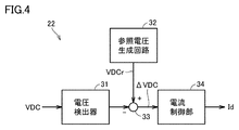
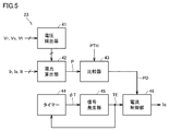
- FIG. 2 is a circuit block diagram showing a configuration of a portion related to control of a converter in the control device shown in FIG. 1. It is a block diagram which shows the structure of the active current command part shown in FIG. It is a block diagram which shows the structure of the reactive current command part shown in FIG. 3 is a circuit block diagram showing a configuration of a failure detector included in the control device shown in FIG. 1.
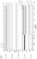
- FIG. 7 is a time chart showing an operation of the uninterruptible power supply device shown in FIGS. 1 to 6.
- FIG. 7 is a block diagram showing a modification of the first embodiment.
- FIG. 6 is a circuit diagram showing a main part of an uninterruptible power supply according to a second embodiment. It is a circuit block diagram which shows the structure of the failure detector of the uninterruptible power supply shown in FIG.
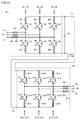
- FIG. 9 is a circuit diagram showing a main part of an uninterruptible power supply according to a third embodiment. It is a circuit block diagram which shows the structure of the failure detector of the uninterruptible power supply shown in FIG.
- FIG. 1 is a circuit block diagram showing a configuration of an uninterruptible power supply according to Embodiment 1 of the present invention.
- this uninterruptible power supply system includes capacitors C1 to C6, Cd, reactors L1 to L6, current detectors CT1 to CT6, a converter 1, a DC positive bus Lp, a DC negative bus Ln, a bidirectional chopper 2, and an inverter 3.
- the operation unit 4, the control device 5, and the notification unit 6 are provided.
- This uninterruptible power supply receives commercial-phase three-phase AC power from the commercial AC power supply 9, and supplies commercial-frequency three-phase AC power to the load 10.
- the commercial AC power supply 9 outputs three-phase AC voltages Vu, Vv, Vw to the AC output terminals 9a-9c, respectively.
- the instantaneous values of the three-phase AC voltages Vu, Vv, Vw are detected by the control device 5.
- the control device 5 detects, based on the AC output voltages Vu, Vv, Vw of the commercial AC power supply 9, whether or not a power failure of the commercial AC power supply 9 has occurred.
- the AC input terminals 10a to 10c of the load 10 receive the three-phase AC voltages Vr, Vs, Vt from the uninterruptible power supply.
- the load 10 is driven by the three-phase AC power supplied from the uninterruptible power supply.
- One electrodes of the capacitors C1 to C3 are connected to the AC output terminals 9a to 9c of the commercial AC power source 9, respectively, and the other electrodes thereof are connected to each other.
- Reactors L1 to L3 have one terminals connected to AC output terminals 9a to 9c of commercial AC power supply 9, respectively, and the other terminals connected to three input nodes of converter 1, respectively.
- the capacitors C1 to C3 and the reactors L1 to L3 form an AC filter 7.
- the AC filter 7 is a low-pass filter and allows an AC current of commercial frequency to flow from the commercial AC power supply 9 to the converter 1 to prevent a signal of a switching frequency from flowing from the converter 1 to the commercial AC power supply 9.
- the current detectors CT1 to CT3 detect the alternating currents Iu, Iv, and Iw flowing in the reactors L1 to L3, respectively, and give a signal indicating the detected values to the control device 5.
- the positive output node of the converter 1 is connected to the positive input node of the inverter 3 via the DC positive bus Lp.
- the negative output node of converter 1 is connected to the negative input node of inverter 3 via DC negative bus Ln.
- Capacitor Cd is connected between buses Lp and Ln, and smoothes DC voltage VDC between buses Lp and Ln. The instantaneous value of DC voltage VDC is detected by control device 5.
- the converter 1 is controlled by the control device 5, and when the three-phase AC power is normally supplied from the commercial AC power supply 9 (when the commercial AC power supply 9 is healthy), the three-phase AC power from the commercial AC power supply 9 is supplied. To DC power.
- the DC power generated by converter 1 is supplied to bidirectional chopper 2 and inverter 3 via buses Lp and Ln.
- the controller 5 controls the converter 1 so that the voltage VDC between the terminals of the capacitor Cd becomes the reference voltage VDCr when the commercial AC power source 9 is healthy.
- the operation of the converter 1 is stopped.
- the converter 1 includes 3 ⁇ N circuit breakers B1 to B3 respectively corresponding to three phases, six IGBTs (Insulated Gate Bipolar Transistors) Q1 to Q6, and six diodes D1 to And D6.
- N the number of circuit breakers B1 to B3 are connected to the input nodes 1a, 1b and 1c, respectively.
- Input nodes 1a, 1b and 1c are connected to the other terminals of reactors L1 to L3 (FIG. 1), respectively.
- the collectors of the IGBTs Q1 to Q3 are all connected to the DC positive bus Lp, and their emitters are connected to the other terminals of the circuit breakers B1 to B3, respectively.
- the collectors of IGBTs Q4 to Q6 are connected to the other terminals of circuit breakers B1 to B3, respectively, and their emitters are both connected to DC negative bus Ln.
- the diodes D1 to D6 are connected in antiparallel to the IGBTs Q1 to Q6, respectively.
- circuit breakers B1 to B3 are conducting.
- Circuit breaker B1 becomes non-conductive when an overcurrent (a predetermined current larger than the rated current) flows between input node 1a and a connection node of IGBTs Q1, Q4.
- Circuit breaker B2 becomes non-conductive when an overcurrent flows between input node 2a and a connection node of IGBTs Q2 and Q5.
- Circuit breaker B3 becomes non-conductive when an overcurrent flows between input node 3a and a connection node of IGBTs Q3 and Q6.
- Circuit breakers B1 to B3 prevent the IGBTs Q1 to Q6 and the diodes D1 to D6 from being destroyed by overcurrent. If the circuit breakers B1 to B3 are not present, for example, if the IGBT Q1 is short-circuited, the input nodes 1a to 1c are short-circuited via the IGBT Q2 and the diode D3, and finally the IGBTs Q1 to Q6 and the diodes D1 to D6 are overcurrent. Destroyed by.
- the circuit breakers B1 to B3 are basically provided in order to prevent the damage from expanding when a short-circuit failure occurs in any one of the IGBTs Q1 to Q6.
- Each of the circuit breakers B1 to B3 includes, for example, a fuse that is blown (blown) when an overcurrent flows. Even if no overcurrent flows, the fuse may be broken due to its deterioration over time (life). The blown fuse is fixed to the non-conducting state and does not return to the conducting state, so that it is treated as a broken circuit breaker. The conductive fuse is treated as a normal circuit breaker.
- Each of the circuit breakers B1 to B3 may include a switch that becomes non-conductive when an overcurrent flows and returns to a conductive state when the overcurrent stops flowing.
- a switch that fails and is fixed in a non-conducting state is treated as a broken circuit breaker.
- the conductive switch is treated as a normal circuit breaker.
- IGBT constitutes a switching element.
- the IGBTs Q1 and Q4 are controlled by the gate signals G1 and G4, the IGBTs Q2 and Q5 are controlled by the gate signals G2 and G5, and the IGBTs Q3 and Q6 are controlled by the gate signals G3 and G6, respectively.
- the gate signals G4 to G6 are inverted signals of the gate signals G1 to G3, respectively.
- the IGBTs Q1 to Q3 are turned on when the gate signals G1 to G3 are set to the “H” level, and turned off when the gate signals G1 to G3 are set to the “L” level, respectively.
- the IGBTs Q4 to Q6 are turned on when the gate signals G4 to G6 are set to the “H” level, and are turned off when the gate signals G4 to G6 are set to the “L” level.
- Each of the gate signals G1 to G6 is a pulse signal train and is a PWM (Pulse Width Modulation) signal.
- the phases of the gate signals G1 and G4, the phases of the gate signals G2 and G5, and the phases of the gate signals G3 and G6 are basically shifted by 120 degrees.
- the gate signals G1 to G6 are generated by the control device 5.
- the IGBTs Q1 and Q5 are turned on, and the breaker B1, the IGBT Q1, the DC positive bus Lp, the capacitor Cd, the DC negative bus Ln are input from the input node 1a.
- IGBTQ5, and circuit breaker B2 cause a current to flow to the input node 1b to charge the capacitor Cd.
- the three-phase AC voltage applied to the input nodes 1a to 1c can be obtained. It is possible to convert to a DC voltage VDC (voltage between terminals of the capacitor Cd).
- the control device 5 determines whether or not the circuit breakers B1 to B3 are normal (conducting state) based on the AC input currents Iu, Iv, and Iw of the converter 1, and a signal indicating the determination result.
- Output DT When circuit breakers B1 to B3 are normal, signal DT is set to the inactive level "L" level. When the circuit breakers B1 to B3 are not normal, the signal DT is set to the activation level "H" level. A method for determining whether or not the circuit breakers B1 to B3 are normal will be described later in detail.
- the bidirectional chopper 2 is controlled by the control device 5, stores the DC power generated by the converter 1 in the battery 11 when the commercial AC power supply 9 is healthy, and responds to the occurrence of the power failure of the commercial AC power supply 9 by the battery.
- the DC power of 11 is supplied to the inverter 3 via the buses Lp and Ln.
- the instantaneous value of the terminal voltage VB of the battery 11 is detected by the control device 5.
- the control device 5 controls the bidirectional chopper 2 so that the terminal voltage VB of the battery 11 becomes the reference voltage VBr when the commercial AC power source 9 is healthy, and when the commercial AC power source 9 has a power failure, the terminal voltage of the capacitor Cd.
- the bidirectional chopper 2 is controlled so that VDC becomes the reference voltage VDCr.
- the inverter 3 is controlled by the control device 5 and converts the DC power supplied from the converter 1 and the bidirectional chopper 2 into three-phase AC power of commercial frequency.
- the three output nodes of inverter 3 are connected to one terminals of reactors L4 to L6, respectively.
- the other terminals of reactors L4 to L6 are connected to three AC input terminals 10a to 10c of load 10, respectively.
- One electrodes of capacitors C4 to C6 are connected to the other terminals of reactors L4 to L6, respectively, and the other electrodes of capacitors C4 to C6 are both connected to the other electrodes of capacitors C1 to C3.
- the capacitors C4 to C6 and the reactors L4 to L6 form an AC filter 8.
- the AC filter 8 is a low-pass filter and allows an AC current of commercial frequency to flow from the inverter 3 to the load 10 to prevent a signal of the switching frequency from flowing from the inverter 3 to the load 10.
- the AC filter 8 converts the three-phase rectangular wave voltage output from the inverter 3 into sinusoidal three-phase AC voltages Vr, Vs, Vt.
- the instantaneous values of the three-phase AC voltages Vr, Vs, Vt are detected by the control device 5.
- the current detectors CT4 to CT6 detect the alternating currents Ir, Is, It flowing through the reactors L4 to L6, respectively, and give signals indicating the detected values to the control device 5.
- the control device 5 is based on the AC output voltages Vu, Vv, Vw of the commercial AC power supply 9, the AC output voltages Vr, Vs, Vt of the inverter 3, and the AC currents Ir, Is, It, and the AC output voltages Vr, Vs, Vt. Inverter 3 is controlled so that each becomes AC output voltage Vu, Vv, Vw.
- the inverter 3 includes IGBTs Q11 to Q16, diodes D11 to D16, and circuit breakers B11 to B13.
- the IGBT constitutes a switching element.
- the collectors of IGBTs Q11 to Q13 are all connected to DC positive bus Lp.
- the collectors of the IGBTs Q14 to Q16 are connected to the emitters of the IGBTs Q11 to Q13, respectively, and the emitters of the IGBTs Q14 to Q16 are all connected to the DC negative bus Ln.
- the diodes D11 to D16 are connected in antiparallel with the IGBTs Q11 to Q16, respectively.
- One terminals of the circuit breakers B11 to B13 are connected to the emitters of the IGBTs Q11 to Q13, respectively, and the other terminals thereof are connected to the output nodes 3a, 3b and 3c, respectively.
- Output nodes 3a, 3b, 3c are connected to one terminals of reactors L4 to L6 (FIG. 1), respectively.
- circuit breakers B11 to B13 are conducting.
- Circuit breaker B11 becomes non-conductive when an overcurrent (a predetermined current larger than the rated current) flows between the connection node of IGBTs Q11 and Q14 and output node 3a.
- Circuit breaker B12 becomes non-conductive when an overcurrent flows between the connection node of IGBTs Q12 and Q15 and output node 3b.
- Circuit breaker B13 becomes non-conductive when an overcurrent flows between the connection node of IGBTs Q13 and Q16 and output node 3c.
- the circuit breakers B11 to B13 prevent the IGBTs Q11 to Q16, the diodes D11 to D16, etc. from being destroyed by the overcurrent.
- Each of the circuit breakers B11 to B13 includes, for example, a fuse that is blown (blown) when an overcurrent flows.
- Each of the circuit breakers B11 to B13 may include a switch that becomes non-conductive when an overcurrent flows and returns to a conductive state when the overcurrent stops flowing.
- the IGBTs Q11 and Q14 are controlled by the gate signals G11 and G14
- the IGBTs Q12 and Q15 are controlled by the gate signals G12 and G15
- the IGBTs Q13 and Q16 are controlled by the gate signals G13 and G16, respectively.
- the gate signals G14 to G16 are inverted signals of the gate signals G11 to G13, respectively.
- the IGBTs Q11 to Q13 are turned on when the gate signals G11 to G13 are set to “H” level, and turned off when the gate signals G11 to G13 are set to “L” level, respectively.
- the IGBTs Q14 to Q16 are turned on when the gate signals G14 to G16 are set to the “H” level, and are turned off when the gate signals G14 to G16 are set to the “L” level.
- Each of the gate signals G11 to G16 is a pulse signal train and is a PWM signal.
- the phases of the gate signals G11 and G14, the phases of the gate signals G12 and G15, and the phases of the gate signals G13 and G16 are basically shifted by 120 degrees.
- the gate signals G11 to G16 are generated by the control device 5.
- DC positive bus Lp is connected to output node 3a via IGBT Q11
- output node 3b is connected to DC negative bus Ln via IGBT Q15, and between output nodes 3a and 3b. Positive voltage is output.
- the DC positive bus Lp is connected to the output node 3b via the IGBT Q12
- the output node 3a is connected to the DC negative bus Ln via the IGBT Q14, and between the output nodes 3a and 3b. Negative voltage is output.
- the DC voltage VDC between the bus lines Lp and Ln is changed to a three-phase AC voltage. It is possible to convert into Vr, Vs, and Vt.
- the operation unit 4 includes a plurality of buttons operated by a user of the uninterruptible power supply, an image display unit that displays various information, and the like. By operating the operation unit 4 by the user, the power of the uninterruptible power supply can be turned on and off, and various conditions can be set.
- the control device 5 controls the signal from the operation unit 4, the AC output voltages Vu, Vv, Vw of the commercial AC power source 9, the AC input currents Iu, Iv, Iw, the terminal voltage VDC of the capacitor Cd, and the terminal voltage VB of the battery 11. ,
- the entire uninterruptible power supply device is controlled based on the AC output currents Ir, Is, It, the AC output voltages Vr, Vs, Vt, and the like.
- the notification unit 6 When the signal DT from the control device 5 is set to the activation level “H” level, the notification unit 6 causes the breakers B1 to B3 in the converter 1 to malfunction due to sound, light, images, or the like. Notify the user of the uninterruptible power supply.
- the converter 1 is controlled so that the terminal voltage VDC of the capacitor Cd becomes the reference voltage VDCr, and the bidirectional chopper 2 controls so that the terminal voltage VB of the battery 11 becomes the reference voltage VBr.
- the inverter 3 is controlled so that the AC output voltages Vr, Vs, Vt become the AC output voltages Vu, Vv, Vw of the commercial AC power supply 9, respectively.
- the load 10 is driven by the AC output voltages Vr, Vs, Vt supplied from the uninterruptible power supply.
- the notification unit 6 notifies the user of the uninterruptible power supply to that effect.
- the faulty circuit breaker is replaced with a new one by the user of the uninterruptible power supply.
- the operation of the converter 1 is stopped, the bidirectional chopper 2 is controlled so that the terminal voltage VDC of the capacitor Cd becomes the reference voltage VDCr, and the DC power of the battery 11 is changed. It is converted into three-phase AC power by the inverter 3 and supplied to the load 10.
- the inspection method of the circuit breakers B1 to B3 which is a feature of the present invention, will be described.
- the circuit breaker B1 fails, the uninterruptible power supply will not operate normally even if other parts are normal.
- the DC voltage VDC can be maintained at the reference voltage VDCr when the load current is small, the DC voltage VDC cannot be maintained at the reference voltage VDCr when the load current increases. Therefore, it is necessary to inspect whether or not the circuit breakers B1 to B3 are normal.
- Iu+Iv -Iw
- Iv+Iw -Iu
- Iw+Iu -Iv
- Iu+Iv, Iv+Iw, and Iw+Iu which are the sums of the combinations of two currents of Iu, Iv, and Iw, do not become 0.
- Iu, Iv, and Iw are detected by the current detectors CT1 to CT3 (FIG. 1), Iu and Iv are added to obtain I1, and Iv and Iw are added to obtain I2. , Iw and Iu are added to obtain I3, and each of I1 to I3 is compared with a sufficiently small threshold current ITH. Then, if any of I1 to I3 is smaller than the threshold current ITH, it is determined that one of the circuit breakers B1 to B3 is out of order. When each of I1 to I3 is larger than the threshold current ITH, it is determined that the circuit breakers B1 to B3 are not broken.
- each of I1 to I3 is less than the threshold current ITH even when the circuit breakers B1 to B3 are normal. Becomes smaller, and it becomes impossible to judge whether or not the circuit breakers B1 to B3 are normal.
- the commercial AC power supply 9 converts the converter 1 to the converter 1.
- the converter 1 is controlled so that a reactive current flows through the circuit 1, and I1 to I3 are increased by the amount of the reactive current to determine whether or not the circuit breakers B1 to B3 are normal. Therefore, according to the first embodiment, it is possible to determine whether or not the circuit breakers B1 to B3 are normal even when there is no load.
- FIG. 3 is a block diagram showing a configuration of a portion related to control of converter 1 in control device 5 shown in FIG.
- the control device 5 includes a voltage detector 20, a phase detector 21, an active current command unit (first command unit) 22, a reactive current command unit (second command unit) 23, a DQ-UVW conversion unit.
- a (two-phase/three-phase conversion unit) 24, subtractors 25a to 25c, a current control circuit 26, adders 27a to 27c, a PWM circuit 28, and a gate circuit 29 are included.
- the voltage detector 20 detects the instantaneous value of the three-phase AC voltage Vu, Vv, Vw supplied from the commercial AC power supply 9, and outputs a signal indicating the detected value.
- the phase detector 21 generates a phase detection value ⁇ indicating the phases of the three-phase AC voltages Vu, Vv, Vw based on the output signal of the voltage detector 20.
- the active current command unit 22 generates the d-axis current command value Id (active current command value) so that the inter-terminal voltage VDC of the capacitor Cd becomes the reference voltage VDCr.
- the active current command unit 22 includes a voltage detector 31, a reference voltage generation circuit 32, a subtractor 33, and a current control unit 34.
- the voltage detector 31 detects the instantaneous value of the voltage VDC between the terminals of the capacitor Cd and outputs a signal indicating the detected value.
- the reference voltage generation circuit 32 generates the reference voltage VDCr.
- the current control unit 34 calculates the d-axis current command value Id by, for example, performing a proportional calculation or a proportional integral calculation on the deviation ⁇ VDC.
- the reactive current command unit 23 generates a q-axis current command value Iq (reactive current command value) for inspecting the circuit breakers B1 to B3.
- the reactive current command unit 23 includes a voltage detector 41, a power calculation unit 42, a comparator 43, a timer 44, a signal generator 45, and a current control unit 46.
- the voltage detector 41 detects the instantaneous value of the three-phase AC voltage Vr, Vs, Vt output from the uninterruptible power supply and outputs a signal indicating the detected value.
- the power calculator 42 calculates the power consumption P of the load 10 based on the output signal of the voltage detector 41 and the output signals of the current detectors CT4 to CT6 (FIG. 1).
- the comparator 43 compares the power consumption P of the load 10 with a predetermined threshold power PTH (for example, a power value of 30% of the rated load), and outputs a signal PD indicating the comparison result.
- a predetermined threshold power PTH for example, a power value of 30% of the rated load
- the timer 44 When the power of the uninterruptible power supply is turned on, the timer 44 starts measuring time, and outputs the output signal ⁇ T in response to the measured time reaching a predetermined first time (for example, one month). Start up from “L” level to "H” level. The measurement time of the timer 44 is reset when the test signal TE is raised from the “L” level to the “H” level.
- the signal generator 45 raises the test signal TE from the “L” level to the “H” level in response to the rise of the output signal ⁇ T of the timer 44 from the “L” level to the “H” level, and sets the predetermined level. After a second time (for example, 10 seconds) has passed, the test signal TE is lowered from the “H” level to the “L” level. The test signal TE is used as a reset signal for the timer 44 and is also given to the current controller 46. The second time is shorter than the first time.
- the current control unit 46 generates a q-axis current command value Iq (reactive current command value) based on the signals PD and TE.
- Iq reactive current command value
- Iq When the signal PD is at the “L” level (when P ⁇ PTH), Iq is set to 0 during the period when the test signal TE is at the “L” level, and when the test signal TE is at the “H” level. Iq is set to a predetermined value Iq0. Iq0 is set so that a reactive current having a delay power factor flows from the commercial AC power supply 9 to the converter 1. This is because the three-phase AC voltages Vu, Vv, and Vw may rise when the reactive current having the power factor flows from the commercial AC power supply 9 to the converter 1.
- the DQ-UVW conversion unit 24 determines the d-axis current command value Id and the q-axis current command value Iq based on the phase detection value ⁇ from the phase detector 21 as the three-phase AC current command value Iuc, Convert to Ivc and Iwc.
- the current control circuit 26 generates the voltage command values Vu1, Vv1, Vw1 so that the deviations ⁇ Iu, ⁇ Iv, ⁇ Iw are zero.
- Current control circuit 26 generates voltage command values Vu1, Vv1, Vw1 by, for example, performing proportional control or proportional-integral control of deviations ⁇ Iu, ⁇ Iv, ⁇ Iw.
- the adder 27a adds the voltage command value Vu1 and the AC voltage Vu detected by the voltage detector 20 to generate a voltage command value Vu2.
- the adder 27b adds the voltage command value Vv1 and the AC voltage Vv detected by the voltage detector 20 to generate a voltage command value Vv2.
- the adder 27c adds the voltage command value Vw1 and the AC voltage Vw detected by the voltage detector 20 to generate a voltage command value Vw2.
- the PWM circuit 28 generates PWM control signals ⁇ 1 to ⁇ 3 for controlling the converter 1 based on the voltage command values Vu2 to Vw2.
- Gate circuit 29 generates gate signals G1 to G6 (FIG. 2) based on PWM control signals ⁇ 1 to ⁇ 3.
- FIG. 6 is a circuit block diagram showing the configuration of the failure detector 50 (determiner) included in the control device 5 shown in FIG.
- the failure detector 50 is a circuit that determines whether or not the circuit breakers B1 to B3 are normal.
- the fault detector 50 includes adders 51 to 53, comparators 54 to 56, OR gates 57 and 58, an AND gate 59, and a latch circuit 60.
- the comparator 54 compares the magnitude (eg, effective value) of the alternating current I1 with the threshold current ITH and outputs a signal ⁇ 54 indicating the comparison result.
- I1>ITH signal ⁇ 54 attains the "L” level.
- I1 ⁇ ITH signal ⁇ 54 attains the “H” level.
- the threshold current ITH is a value sufficiently smaller than the rated current and close to 0A.
- the comparator 55 compares the magnitude (for example, the effective value) of the alternating current I2 with the magnitude of the threshold current ITH, and outputs a signal ⁇ 55 indicating the comparison result.
- I2>ITH signal ⁇ 55 attains the “L” level.
- I2 ⁇ ITH signal ⁇ 55 attains the “H” level.
- the comparator 56 compares the magnitude (eg, effective value) of the AC current I3 with the threshold current ITH and outputs a signal ⁇ 56 indicating the comparison result.
- I3>ITH signal ⁇ 56 attains the "L” level.
- I3 ⁇ ITH signal ⁇ 56 attains the “H” level.
- the OR gate 57 outputs the logical sum signal ⁇ 57 of the output signals ⁇ 54 to ⁇ 56 of the comparators 54 to 56.
- signal ⁇ 57 attains the “H” level.
- signal ⁇ 57 attains "L” level.
- the OR gate 58 outputs a logical sum signal ⁇ 58 of the signal PD and the test signal TE.
- signal PD attains an "H” level
- signal .phi.58 attains an activation level “H” level regardless of test signal TE.
- the signal PD is at the “L” level and the signal ⁇ 58 is activated only while the test signal TE is at the activation level “H” level. The level becomes “H” level.
- AND gate 59 outputs a logical product signal ⁇ 59 of signals ⁇ 57 and ⁇ 58.
- the output signal ⁇ 57 of the OR gate 57 passes through the AND gate 59 and becomes the signal ⁇ 59 only while the output signal ⁇ 58 of the OR gate 58 is at the "H" level of the activation level.
- the latch circuit 60 is reset by the reset signal RE to set the signal DT (FIG. 1) to the “L” level and changes the signal DT to “H” level from the “L” level to the “H” level. "H” level. For example, when the user of the uninterruptible power supply presses the reset button of the operation unit 4 (FIG. 1), the operation unit 4 outputs the reset signal RE to the latch circuit 60.
- the voltage detector 41 detects the AC output voltages Vr, Vs, Vt, and the current detectors CT4 to CT6 (FIG. 1) detect the AC output currents Ir, Is, It.
- the power consumption P of the load 10 is calculated by the power calculator 42, and the power P and the threshold power PTH are compared by the comparator 43 to generate the signal PD indicating the comparison result.
- the timer 44 and the signal generator 45 set the test signal TE to the activation level "H" level for 10 seconds (second time) of one month (first time), for example.
- the current control unit 46 sets the q-axis current command value Iq to 0.
- P ⁇ PTH the current control unit 46 sets the q-axis current command value Iq to the predetermined value Iq0 only while the signal PD is at “L” level and the test signal TE is at “H” level. ..
- the d-axis current command value Id and the q-axis current command value Iq are determined by the DQ-UVW converter 24 based on the phase detection value ⁇ detected by the phase detector 21. Converted to Iuc, Ivc, and Iwc.
- the deviations ⁇ Iu, ⁇ Iv, ⁇ Iw between the three-phase AC current command values Iuc, Ivc, Iwc and the AC input currents Iu, Iv, Iw detected by the current detectors CT1 to CT3 are obtained by the subtracters 25a to 25c.
- the current control circuit 26 generates the voltage command values Vu1, Vv1, Vw1 so that the deviations ⁇ Iu, ⁇ Iv, ⁇ Iw become 0, and the voltage command values Vu1, Vv1, Vw1 and the AC input voltage Vu detected by the voltage detector 20. , Vv, Vw are added by adders 27a to 27c to generate voltage command values Vu2, Vv2, Vw2.
- the PWM control signals ⁇ 1 to ⁇ 3 for controlling the converter 1 are generated by the PWM circuit 28 based on the voltage command values Vu2 to Vw2.
- Gate circuit 29 generates gate signals G1 to G6 (FIG. 2) based on PWM control signals ⁇ 1 to ⁇ 3, and converter 1 is driven.
- the signals ⁇ 54 to ⁇ 56 are at "H" level, and when I1 to I3 are larger than the threshold current ITH, the signals ⁇ 54 to ⁇ 56 are at "L" level. ..
- the notification unit 6 (FIG. 1) notifies the user of the uninterruptible power supply that any of the circuit breakers B1 to B3 has failed.
- the failure detector 50 using the operation unit 4 (FIG. 1), the reset signal RE is given to the latch circuit 60, the latch circuit 60 is reset, and the signal DT becomes the “L” level.
- the signal ⁇ 58 becomes the “H” level and the signal ⁇ 57 passes through the AND gate 59 to become the signal DT only when the test signal TE is at the “H” level.
- the uninterruptible power supply is in the no-load state and the test signal TE is at the “L” level, the AC input currents Iu, Iv, and Iw are small, and the signals ⁇ 54 to ⁇ 56 are all at the “H” level and the signal ⁇ 57. Becomes "H" level.
- the signal PD is at "L” level
- the signal TE is at “L” level
- the signal ⁇ 58 is at “L” level
- the signals ⁇ 59 and DT are maintained at “L” level. .. Therefore, even when the uninterruptible power supply system is in a no-load state, it is not erroneously determined that the breakers B1 to B3 are out of order.
- converter 1 is controlled so that a reactive current flows into converter 1 when test signal TE is at “H” level, and AC input current Iu, Iv and Iw are increased.
- I1 to I3 become larger than the threshold current ITH
- the signals ⁇ 54 to ⁇ 56 are all set to the “L” level
- the signals ⁇ 57, ⁇ 59, and DT are set to the “L” level. It becomes a level.
- the notification unit 6 (FIG. 1) notifies the user of the uninterruptible power supply that the circuit breakers B1 to B3 have failed. Therefore, even if the uninterruptible power supply is in a no-load state, it is possible to accurately determine whether or not the circuit breakers B1 to B3 are normal.
- FIGS. 7A to 7E are time charts showing the operation of the uninterruptible power supply in the unloaded state.
- FIGS. 7A to 7E show a state in which the test signal TE is raised from the “L” level to the “H” level at time t1 and the reactive current is supplied to the converter 1.
- FIG. 7A shows the waveforms of the AC output voltage VO, that is, the AC output voltages Vr, Vs, and Vt.
- Each of Vr, Vs, and Vt changes sinusoidally at the commercial frequency, and the phases of Vr, Vs, and Vt are shifted by 120 degrees.
- FIG. 7B shows the waveforms of the AC output current IO, that is, the AC output currents Ir, Is, It. Since there is no load, Ir, Is, and It are all 0A.
- FIG. 7C shows the waveform of the voltage VDC between the terminals of the capacitor Cd. VDC is maintained at the reference voltage VDCr.
- FIG. 7D shows the waveforms of the AC input current Ii, that is, the AC input currents Iu, Iv, and Iw.
- FIG. 7E shows waveforms of the d-axis current command value Id and the q-axis current command value Iq.
- the d-axis current command value Id is constantly adjusted so that the inter-terminal voltage VDC of the capacitor Cd becomes the reference voltage VDCr. Since the uninterruptible power supply is in an unloaded state, the swing range of the d-axis current command value Id is small.
- the waveform of the d-axis current command value Id does not change before and after time t1.
- the q-axis current command value Iq is set to 0, and the reactive current flowing into the converter 1 is set to 0A.
- the q-axis current command value Iq is set to the predetermined value Iq0, and the reactive current for inspecting the circuit breakers B1 to B3 flows through the converter 1. During the period when the reactive current is flowing into the converter 1, it is checked whether or not the circuit breakers B1 to B3 are normal, and the signal DT indicating the test result is output.
- the time for which the reactive current is passed through the converter 1 is set to one cycle or more, for example, 10 seconds. If a reactive current is passed through the converter 1 for a long time, the loss in the circuit through which the reactive current flows (AC filter 7, converter 1, etc.) increases, and the rated current of the parts used increases, which leads to larger parts and higher prices. Because it invites.
- the reactive current for inspecting the circuit breakers B1 to B3 is passed from the commercial AC power supply 9 to the converter 1, so that the uninterruptible power supply does not operate. Even in the case of load, it is possible to detect the failure of the circuit breakers B1 to B3.
- the reactive current is passed through the converter 1 for a predetermined time (for example, 10 seconds) in a predetermined cycle (for example, one month), so that the loss generated in the circuit through which the reactive current flows is suppressed to a small level, and The rated current of parts can be suppressed to a small value.
- the reactive current having the delayed power factor is passed through the converter 1, the AC input voltages Vu, Vv, Vw do not rise.
- the failure of the circuit breakers B1 to B3 can be detected by using the active current flowing into the converter 1 without supplying the reactive current to the converter 1.
- FIG. 8 is a block diagram showing a modification of the first embodiment, which is compared with FIG. Referring to FIG. 8, the difference between this modification and the first embodiment is that reactive current command unit 23 is replaced with reactive current command unit 23A.
- the reactive current command unit 23A replaces the voltage detector 41, the power calculation unit 42, and the comparator 43 of the reactive current command unit 23 with a voltage detector 61, a current detector 62, a power calculation unit 63, and a comparator 64. It is a thing.
- the voltage detector 61 detects the instantaneous value of the voltage VDC between the terminals of the capacitor Cd and outputs a signal indicating the detected value.
- Current detector 62 detects the instantaneous value of the DC output current (for example, DC current flowing through DC positive bus Lp) IDC of converter 1 and outputs a signal indicating the detected value.
- the comparator 64 compares the electric power Pd with the threshold electric power PTHd and outputs a signal PD indicating the comparison result.
- Pd>PTH the signal PD becomes "H” level.
- Pd ⁇ PTH the signal PD becomes "L” level.
- FIG. 9 is a circuit diagram showing a main part of an uninterruptible power supply according to a second embodiment of the present invention, and is a diagram to be compared with FIG.
- the uninterruptible power supply device differs from the uninterruptible power supply device of the first embodiment in that converter 1 and inverter 3 are replaced with converter 1A and inverter 3A, respectively.
- Converter 1A includes 3 ⁇ N circuit breakers B4 to B9, IGBTs Q1 to Q6, and diodes D1 to D6.
- N is 2.
- Circuit breakers B4 and B7, circuit breakers B5 and B8, and circuit breakers B6 and B9 form first and second circuit breakers, respectively.
- the IGBTs Q1 and Q4, the IGBTs Q2 and Q5, and the IGBTs Q3 and Q6 form first and second switching elements, respectively.
- One of the terminals of the circuit breakers B4 to B6 is connected to the DC positive bus Lp, the other terminals thereof are connected to the collectors of the IGBTs Q1 to Q3, and the emitters of the IGBTs Q1 to Q3 are connected to the input nodes 1a to 1c, respectively.
- the collectors of the IGBTs Q4 to Q6 are respectively connected to the input nodes 1a to 1c, their emitters are respectively connected to one terminals of the circuit breakers B7 to B9, and the other terminals of the circuit breakers B7 to B9 are both connected to the DC negative bus Ln. It
- the diodes D1 to D6 are connected in antiparallel to the IGBTs Q1 to Q6, respectively.
- circuit breakers B4 to B9 are conducting. Circuit breakers B4 to B9 are rendered non-conductive when an overcurrent flows through IGBTs Q4 to Q6, respectively.
- the circuit breakers B4 to B9 prevent the IGBTs Q1 to Q6, the diodes D1 to D6 and the like from being destroyed by an overcurrent. If the circuit breakers B4 to B9 are not provided, for example, if the IGBT Q1 has a short-circuit fault, the input nodes 1a to 1c are short-circuited via the IGBT Q2 and the diode D3, and finally the IGBT Q1 to Q6 and the diodes D1 to D6 are overcurrent. Destroyed by.
- the circuit breakers B4 to B9 are basically provided in order to prevent the damage from spreading when one of the IGBTs Q1 to Q6 is short-circuited.
- Each of the circuit breakers B4 to B9 includes, for example, a fuse that is blown (blown) when an overcurrent flows. Even if no overcurrent flows, the fuse may be broken due to its deterioration over time (life). The blown fuse is fixed to the non-conducting state and does not return to the conducting state, so that it is treated as a broken circuit breaker. The conductive fuse is treated as a normal circuit breaker.
- each of the circuit breakers B4 to B9 may include a switch that becomes non-conductive when an overcurrent flows and returns to a conductive state when the overcurrent stops flowing.
- a switch that fails and is fixed in a non-conducting state is treated as a broken circuit breaker.
- the conductive switch is treated as a normal circuit breaker.
- the converter 1A is controlled by the gate signals G1 to G6 and converts the three-phase AC voltages Vu, Vv, Vw supplied from the commercial AC power supply 9 into the DC voltage VDC.
- the inverter 3A includes circuit breakers B14 to B19, IGBTs Q11 to Q16, and diodes D11 to D16.
- Circuit breakers B14 to B16 each have one terminal connected to DC positive bus Lp, the other terminals connected to collectors of IGBTs Q11 to Q13, and emitters of IGBTs Q11 to Q13 connected to output nodes 3a to 3c, respectively.
- the collectors of the IGBTs Q14 to Q16 are respectively connected to the output nodes 3a to 3c, their emitters are respectively connected to one terminals of the circuit breakers B17 to B19, and the other terminals of the circuit breakers B17 to B19 are both connected to the DC negative bus Ln. It The diodes D11 to D16 are connected in antiparallel with the IGBTs Q11 to Q16, respectively.
- circuit breakers B14 to B19 are conducting. Circuit breakers B14 to B19 are rendered non-conductive when an overcurrent flows through IGBTs Q11 to Q16, respectively.
- the circuit breakers B14 to B19 prevent the IGBTs Q11 to Q16, the diodes D11 to D16, etc. from being destroyed by the overcurrent. If the circuit breakers B14 to B19 are not provided, for example, if the IGBT Q11 has a short-circuit fault, the output nodes 3a to 3c are short-circuited via the IGBT Q12 and the diode D13, and finally the IGBT Q11 to Q16 and the diodes D11 to D16 are overcurrent. Destroyed by.
- the circuit breakers B14 to B19 are basically provided in order to prevent the damage from spreading when one of the IGBTs Q11 to Q16 has a short-circuit fault.
- Each of the circuit breakers B11 to B13 includes, for example, a fuse that is blown (blown) when an overcurrent flows.
- Each of the circuit breakers B11 to B13 may include a switch that becomes non-conductive when an overcurrent flows and returns to a conductive state when the overcurrent stops flowing.
- the inverter 3A is controlled by the gate signals G11 to G16, and converts the inter-terminal voltage VDC of the capacitor Cd into three-phase AC voltages Vr, Vs, Vt.
- FIG. 10 is a circuit block diagram showing a configuration of a failure detector 50A that inspects whether or not the circuit breakers B4 to B9 in the converter 1A are normal, and is a diagram to be compared with FIG.
- failure detector 50A differs from failure detector 50 of FIG. 6 in that adders 51-53 and comparators 54-56 are LPFs (low-pass filters) 71-73 and comparators. It is a point that is replaced with 74 to 76.
- LPF 71 passes only DC current Idu of AC input current Iu of converter 1A detected by current detector CT1 (FIG. 1).
- the LPF 72 passes only the DC current Idv of the AC input current Iv of the converter 1A detected by the current detector CT2 (FIG. 1).
- the LPF 73 passes only the DC current Idw of the AC input current Iw of the converter 1A detected by the current detector CT3 (FIG. 1).
- the comparator 74 compares the magnitude of the DC current Idu with the magnitude of a predetermined threshold current ITHd and outputs a signal ⁇ 74 indicating the comparison result.
- Idu ⁇ IThd the signal ⁇ 74 is at “L” level.
- Idu>IThd the signal ⁇ 74 is at “H” level.
- the comparator 75 compares the magnitude of the direct current Idv with the magnitude of a predetermined threshold current ITHd and outputs a signal ⁇ 75 indicating the comparison result.
- Idv ⁇ IThd the signal ⁇ 75 is at “L” level.
- Idv>IThd the signal ⁇ 75 is at “H” level.
- the comparator 76 compares the magnitude of the direct current Idw with the magnitude of a predetermined threshold current ITHd and outputs a signal ⁇ 76 indicating the comparison result.
- Idw ⁇ IThd the signal ⁇ 76 is at “L” level.
- Idw>IThd the signal ⁇ 76 is at “H” level.
- Output signals ⁇ 74 to ⁇ 76 of the comparators 74 to 76 are applied to the OR gate 57.
- each of the alternating currents Iu, Iv, and Iw changes in a sine wave shape. Therefore, DC currents Idu, Idv, Iwd included in AC currents Iu, Iv, Iw are all 0A, and output signals ⁇ 74- ⁇ 76 of comparators 74-76 are all at "L” level. Therefore, signals ⁇ 57 and ⁇ 59 both attain the “L” level, and signal DT is maintained at the “L” level.
- the signal PD When the power consumption P of the load 10 is smaller than the threshold power PTH, the signal PD is at the “H” level, and the signals ⁇ 59 and DT are at the “L” level while the test signal TE is at the “L” level. Maintained. That is, while P ⁇ PTH and the test signal TE is at the "L” level, the circuit breakers B4 to B9 are not inspected and the signal DT is set to the "L” level.
- the output signal ⁇ 58 of the OR gate 58 is set to the “H” level. Further, while the test signal TE is at "H” level, a reactive current is supplied from the commercial AC power supply 9 to the converter 1A, and the AC currents Iu, Iv, Iw are increased. By supplying large alternating currents Iu, Iv, Iw to the converter 1A, it is checked whether or not the circuit breakers B4 to B9 are normal. The inspection method at this time is the same as in the case of P>PTH. Other configurations and operations are the same as those in the first embodiment, and therefore description thereof will not be repeated.
- the reactive current for inspecting the circuit breakers B4 to B9 is supplied from the commercial AC power supply 9 to the converter 1A, so that the uninterruptible power supply does not operate. Even in the case of load, it is possible to detect the failure of the circuit breakers B4 to B9.
- the reactive current is passed through the converter 1A for a predetermined time (for example, 10 seconds) in a predetermined cycle (for example, one month), so that the loss generated in the circuit through which the reactive current flows is suppressed to a small level, and The rated current of parts can be suppressed to a small value.
- FIG. 11 is a circuit diagram showing a main part of an uninterruptible power supply device according to a third embodiment of the present invention, and is a diagram to be compared with FIG. 9.
- the uninterruptible power supply device differs from the uninterruptible power supply device of the second embodiment in that converter 1A and inverter 3A are replaced with converter 1B and inverter 3B, respectively.
- the converter 1B is a converter 1A with circuit breakers B1 to B3 added. Circuit breakers B1 to B3 have one terminals connected to input nodes 1a to 1c, respectively, and the other terminals connected to the emitters of IGBTs Q1 to Q3, respectively.
- the converter 1B is a combination of the converter 1 (FIG. 2) and the converter 1A (FIG. 9).
- converter 1B is controlled by gate signals G1 to G6 and converts three-phase AC voltages Vu, Vv, Vw supplied from commercial AC power supply 9 into DC voltage VDC.
- the inverter 3B is one in which circuit breakers B11 to B13 are added to the inverter 3A. Circuit breakers B11-B13 have one terminals connected to the emitters of IGBTs Q11-Q13, respectively, and the other terminals connected to output nodes 3a-3c, respectively.
- the inverter 3B is a combination of the inverter 3 (FIG. 2) and the inverter 3A (FIG. 9).
- the inverter 3B is controlled by the gate signals G11 to G16 and converts the inter-terminal voltage VDC of the capacitor Cd into three-phase AC voltages Vr, Vs, Vt.
- FIG. 12 is a circuit block diagram showing a configuration of a failure detector 80 that inspects whether or not the circuit breakers B1 to B9 in the converter 1B are normal. 12, failure detector 80 includes failure detector 50 of the first embodiment (FIG. 6), failure detector 50A of the second embodiment (FIG. 10), and OR gate 81.
- the output signal DT1 of the failure detector 50 is set to the “H” level. If any of the circuit breakers B4 to B9 in converter 1B fails, the output signal DT2 of failure detector 50B is set to "H” level.
- the OR gate 81 outputs a logical sum signal DT of the signals DT1 and DT2. Therefore, if any of the circuit breakers B1 to B9 in converter 1B fails, the output signal DT of failure detector 80 is set to the “H” level.
Landscapes
- Engineering & Computer Science (AREA)
- Power Engineering (AREA)
- Inverter Devices (AREA)
- Rectifiers (AREA)
Abstract
無停電電源装置の制御装置(5)は、コンバータ(1)の直流出力電圧が参照電圧になるようにd軸電流指令値を生成し、コンバータ内に設けられた3個の遮断器(B1~B3)が正常であるか否かを検査するためにq軸電流指令値を生成し、d軸電流指令値およびq軸電流指令値を三相交流電流指令値に変換し、コンバータに流入する三相交流電流が三相交流電流指令値になるようにコンバータを制御し、三相交流電流に基づいて3個の遮断器が正常であるか否かを判定する。
Description
この発明は電力変換装置に関し、特に、コンバータ内の複数の遮断器が正常か否かを判定する判定器を備えた電力変換装置に関する。
たとえば特開2000-175454号公報(特許文献1)には、交流電源から供給される三相交流電圧を直流電圧に変換するコンバータと、コンバータ内に設けられた複数の遮断器と、交流電源からコンバータに流れる三相交流電流を検出する電流検出器と、電流検出器の検出結果に基づいて複数の遮断器が正常であるか否かを判定する判定器とを備えた電力変換装置が開示されている。
しかし、特許文献1では、電力変換装置が無負荷である場合には、交流電源からコンバータに流れる三相交流電流が小さいので、複数の遮断器が正常であるか否かを判定することができないという問題があった。
それゆえに、この発明の主たる目的は、無負荷の場合でも複数の遮断器が正常であるか否かを判定することが可能な電力変換装置を提供することである。
この発明に係る電力変換装置は、商用交流電源から供給される三相交流電圧を直流電圧に変換するコンバータと、それぞれ三相に対応してコンバータ内に設けられ、各々が対応する相の過電流を遮断する3×N個の遮断器と、商用交流電源からコンバータに流れる三相交流電流を検出する電流検出器と、コンバータの直流出力電圧が参照電圧になるように有効電流指令値を生成する第1の指令部と、3×N個の遮断器が正常であるか否かを検査するために無効電流指令値を生成する第2の指令部と、有効電流指令値および無効電流指令値を三相交流電流指令値に変換する二相三相変換部と、電流検出器によって検出される三相交流電流がそれぞれ三相交流電流指令値になるようにコンバータを制御する制御部と、電流検出器の検出結果に基づいて、3×N個の遮断器が正常であるか否かを判定する判定器とを備えたものであり、Nは自然数である。
この発明に係る電力変換装置では、複数の遮断器が正常であるか否かを検査するための無効電流を交流電源からコンバータに流すので、電力変換装置が無負荷の場合でも、複数の遮断器が正常であるか否かを検査することができる。
[実施の形態1]
図1は、この発明の実施の形態1による無停電電源装置の構成を示す回路ブロック図である。図1において、この無停電電源装置は、コンデンサC1~C6,Cd、リアクトルL1~L6、電流検出器CT1~CT6、コンバータ1、直流正母線Lp、直流負母線Ln、双方向チョッパ2、インバータ3、操作部4、制御装置5、および報知部6を備える。
図1は、この発明の実施の形態1による無停電電源装置の構成を示す回路ブロック図である。図1において、この無停電電源装置は、コンデンサC1~C6,Cd、リアクトルL1~L6、電流検出器CT1~CT6、コンバータ1、直流正母線Lp、直流負母線Ln、双方向チョッパ2、インバータ3、操作部4、制御装置5、および報知部6を備える。
この無停電電源装置は、商用交流電源9から商用周波数の三相交流電力を受け、負荷10に商用周波数の三相交流電力を供給する。商用交流電源9は、交流出力端子9a~9cにそれぞれ三相交流電圧Vu,Vv,Vwを出力する。
三相交流電圧Vu,Vv,Vwの瞬時値は、制御装置5によって検出される。制御装置5は、商用交流電源9の交流出力電圧Vu,Vv,Vwに基づいて、商用交流電源9の停電が発生したか否かを検出する。負荷10の交流入力端子10a~10cは、無停電電源装置から三相交流電圧Vr,Vs,Vtを受ける。負荷10は、無停電電源装置から供給される三相交流電力によって駆動される。
コンデンサC1~C3の一方電極はそれぞれ商用交流電源9の交流出力端子9a~9cに接続され、それらの他方電極は互いに接続される。リアクトルL1~L3の一方端子はそれぞれ商用交流電源9の交流出力端子9a~9cに接続され、それらの他方端子はコンバータ1の3つの入力ノードにそれぞれ接続される。
コンデンサC1~C3およびリアクトルL1~L3は交流フィルタ7を構成する。交流フィルタ7は、低域通過フィルタであり、商用交流電源9からコンバータ1に商用周波数の交流電流を流し、コンバータ1から商用交流電源9にスイッチング周波数の信号が流れることを防止する。電流検出器CT1~CT3は、それぞれリアクトルL1~L3に流れる交流電流Iu,Iv,Iwを検出し、検出値を示す信号を制御装置5に与える。
コンバータ1の正側出力ノードは、直流正母線Lpを介してインバータ3の正側入力ノードに接続される。コンバータ1の負側出力ノードは、直流負母線Lnを介してインバータ3の負側入力ノードに接続される。コンデンサCdは、母線Lp,Ln間に接続され、母線Lp,Ln間の直流電圧VDCを平滑化させる。直流電圧VDCの瞬時値は、制御装置5によって検出される。
コンバータ1は、制御装置5によって制御され、商用交流電源9から三相交流電力が正常に供給されている場合(商用交流電源9の健全時)には、商用交流電源9からの三相交流電力を直流電力に変換する。コンバータ1によって生成された直流電力は、母線Lp,Lnを介して双方向チョッパ2およびインバータ3に供給される。
制御装置5は、商用交流電源9の健全時には、コンデンサCdの端子間電圧VDCが参照電圧VDCrになるようにコンバータ1を制御する。商用交流電源9からの三相交流電力の供給が停止された場合(商用交流電源9の停電時)には、コンバータ1の運転は停止される。
コンバータ1は、図2に示すように、それぞれ三相に対応する3×N個の遮断器B1~B3と、6個のIGBT(Insulated Gate Bipolar Transistor)Q1~Q6と、6個のダイオードD1~D6とを含む。ただし、N=1である。遮断器B1~B3の一方端子は、それぞれ入力ノード1a,1b,1cに接続される。入力ノード1a,1b,1cは、それぞれリアクトルL1~L3(図1)の他方端子に接続される。
IGBTQ1~Q3のコレクタはともに直流正母線Lpに接続され、それらのエミッタはそれぞれ遮断器B1~B3の他方端子に接続される。IGBTQ4~Q6のコレクタはそれぞれ遮断器B1~B3の他方端子に接続され、それらのエミッタはともに直流負母線Lnに接続される。ダイオードD1~D6は、それぞれIGBTQ1~Q6に逆並列に接続される。
初期状態では、遮断器B1~B3は導通している。遮断器B1は、入力ノード1aとIGBTQ1,Q4の接続ノードとの間に過電流(定格電流よりも大きな所定電流)が流れた場合に非導通状態となる。遮断器B2は、入力ノード2aとIGBTQ2,Q5の接続ノードとの間に過電流が流れた場合に非導通状態となる。遮断器B3は、入力ノード3aとIGBTQ3,Q6の接続ノードとの間に過電流が流れた場合に非導通状態となる。
遮断器B1~B3は、過電流によってIGBTQ1~Q6、ダイオードD1~D6などが破壊されることを防止する。もし遮断器B1~B3がない場合、たとえばIGBTQ1が短絡故障した場合、IGBTQ2やダイオードD3を介して入力ノード1a~1cが短絡され、最終的には、IGBTQ1~Q6およびダイオードD1~D6が過電流によって破壊される。遮断器B1~B3は、基本的には、IGBTQ1~Q6のうちのいずれか1つのIGBTが短絡故障した場合に、被害が拡大することを防止するために設けられている。
遮断器B1~B3の各々は、たとえば、過電流が流れた場合にブロー(溶断)されるヒューズを含む。また、過電流が流れなくても、ヒューズは、その経時劣化(寿命)によって断線する場合がある。断線したヒューズは、非導通状態に固定され、導通状態に戻ることはないので、故障した遮断器として扱われる。導通状態のヒューズは、正常な遮断器として扱われる。
また、遮断器B1~B3の各々は、過電流が流れた場合に非導通になり、過電流が流れなくなった場合に導通状態に戻るスイッチを含んでいても構わない。故障して非導通状態に固定されたスイッチは、故障した遮断器として扱われる。導通状態のスイッチは、正常な遮断器として扱われる。
IGBTは、スイッチング素子を構成する。IGBTQ1,Q4はそれぞれゲート信号G1,G4によって制御され、IGBTQ2,Q5はそれぞれゲート信号G2,G5によって制御され、IGBTQ3,Q6はそれぞれゲート信号G3,G6によって制御される。ゲート信号G4~G6は、それぞれゲート信号G1~G3の反転信号である。
IGBTQ1~Q3は、それぞれゲート信号G1~G3が「H」レベルにされた場合にオンし、それぞれゲート信号G1~G3が「L」レベルにされた場合にオフする。IGBTQ4~Q6は、それぞれゲート信号G4~G6が「H」レベルにされた場合にオンし、それぞれゲート信号G4~G6が「L」レベルにされた場合にオフする。
ゲート信号G1~G6の各々は、パルス信号列であり、PWM(Pulse Width Modulation)信号である。ゲート信号G1,G4の位相とゲート信号G2,G5の位相とゲート信号G3,G6の位相とは、基本的には120度ずつずれている。ゲート信号G1~G6は、制御装置5によって生成される。
たとえば、交流入力電圧Vuのレベルが交流入力電圧Vvのレベルよりも高い場合は、IGBTQ1,Q5がオンされ、入力ノード1aから遮断器B1、IGBTQ1、直流正母線Lp、コンデンサCd、直流負母線Ln、IGBTQ5、および遮断器B2を介して入力ノード1bに電流が流れ、コンデンサCdが充電される。
逆に、交流入力電圧Vvのレベルが交流入力電圧Vuのレベルよりも高い場合は、IGBTQ2,Q4がオンされ、入力ノード1bから遮断器B2、IGBTQ2、直流正母線Lp、コンデンサCd、直流負母線Ln、IGBTQ4、および遮断器B1を介して入力ノード1aに電流が流れ、コンデンサCdが充電される。他の場合も同様である。
ゲート信号G1~G6によってIGBTQ1~Q6の各々を所定のタイミングでオンおよびオフさせるとともに、IGBTQ1~Q6の各々のオン時間を調整することにより、入力ノード1a~1cに与えられた三相交流電圧を直流電圧VDC(コンデンサCdの端子間電圧)に変換することが可能となっている。
また、ゲート信号G1~G6によってIGBTQ1~Q6の各々をオンおよびオフさせるタイミングを調整するとともに、IGBTQ1~Q6の各々のオン時間を調整することにより、商用交流電源9からコンバータ1に流れる有効電流および無効電流を調整することが可能となっている。
図1に戻って、制御装置5は、コンバータ1の交流入力電流Iu,Iv,Iwに基づいて遮断器B1~B3が正常(導通状態)であるか否かを判定し、判定結果を示す信号DTを出力する。遮断器B1~B3が正常である場合には、信号DTは非活性化レベルの「L」レベルにされる。遮断器B1~B3が正常でない場合には、信号DTは活性化レベルの「H」レベルにされる。遮断器B1~B3が正常か否かを判定する方法については、後で詳細に説明する。
双方向チョッパ2は、制御装置5によって制御され、商用交流電源9の健全時には、コンバータ1によって生成された直流電力をバッテリ11に蓄え、商用交流電源9の停電が発生したことに応じて、バッテリ11の直流電力を母線Lp,Lnを介してインバータ3に供給する。バッテリ11の端子間電圧VBの瞬時値は、制御装置5によって検出される。
制御装置5は、商用交流電源9の健全時には、バッテリ11の端子間電圧VBが参照電圧VBrになるように双方向チョッパ2を制御し、商用交流電源9の停電時には、コンデンサCdの端子間電圧VDCが参照電圧VDCrになるように双方向チョッパ2を制御する。
インバータ3は、制御装置5によって制御され、コンバータ1および双方向チョッパ2から供給される直流電力を商用周波数の三相交流電力に変換する。インバータ3の3つの出力ノードは、それぞれリアクトルL4~L6の一方端子に接続される。リアクトルL4~L6の他方端子は、それぞれ負荷10の3つの交流入力端子10a~10cに接続される。コンデンサC4~C6の一方電極はそれぞれリアクトルL4~L6の他方端子に接続され、コンデンサC4~C6の他方電極はともにコンデンサC1~C3の他方電極に接続される。
コンデンサC4~C6およびリアクトルL4~L6は交流フィルタ8を構成する。交流フィルタ8は、低域通過フィルタであり、インバータ3から負荷10に商用周波数の交流電流を流し、インバータ3から負荷10にスイッチング周波数の信号が流れることを防止する。換言すると、交流フィルタ8は、インバータ3から出力される三相矩形波電圧を正弦波状の三相交流電圧Vr,Vs,Vtに変換する。
三相交流電圧Vr,Vs,Vtの瞬時値は、制御装置5によって検出される。電流検出器CT4~CT6は、それぞれリアクトルL4~L6に流れる交流電流Ir,Is,Itを検出し、検出値を示す信号を制御装置5に与える。
制御装置5は、商用交流電源9の交流出力電圧Vu,Vv,Vw、インバータ3の交流出力電圧Vr,Vs,Vt、および交流電流Ir,Is,Itに基づき、交流出力電圧Vr,Vs,Vtがそれぞれ交流出力電圧Vu,Vv,Vwになるようにインバータ3を制御する。
インバータ3は、図2に示すように、IGBTQ11~Q16、ダイオードD11~D16、および遮断器B11~B13を含む。IGBTは、スイッチング素子を構成する。IGBTQ11~Q13のコレクタはともに直流正母線Lpに接続される。IGBTQ14~Q16のコレクタはそれぞれIGBTQ11~Q13のエミッタに接続され、IGBTQ14~Q16のエミッタはともに直流負母線Lnに接続される。ダイオードD11~D16は、それぞれIGBTQ11~Q16に逆並列に接続される。
遮断器B11~B13の一方端子はそれぞれIGBTQ11~Q13のエミッタに接続され、それらの他方端子はそれぞれ出力ノード3a,3b,3cに接続される。出力ノード3a,3b,3cは、それぞれリアクトルL4~L6(図1)の一方端子に接続される。
初期状態では、遮断器B11~B13は導通している。遮断器B11は、IGBTQ11,Q14の接続ノードと出力ノード3aとの間に過電流(定格電流よりも大きな所定電流)が流れた場合に非導通状態となる。遮断器B12は、IGBTQ12,Q15の接続ノードと出力ノード3bとの間に過電流が流れた場合に非導通状態となる。遮断器B13は、IGBTQ13,Q16の接続ノードと出力ノード3cとの間に過電流が流れた場合に非導通状態となる。遮断器B11~B13は、過電流によってIGBTQ11~Q16、ダイオードD11~D16などが破壊されることを防止する。
遮断器B11~B13の各々は、たとえば、過電流が流れた場合にブロー(溶断)されるヒューズを含む。また、遮断器B11~B13の各々は、過電流が流れた場合に非導通になり、過電流が流れなくなった場合に導通状態に戻るスイッチを含んでいても構わない。
IGBTQ11,Q14はそれぞれゲート信号G11,G14によって制御され、IGBTQ12,Q15はそれぞれゲート信号G12,G15によって制御され、IGBTQ13,Q16はそれぞれゲート信号G13,G16によって制御される。ゲート信号G14~G16は、それぞれゲート信号G11~G13の反転信号である。
IGBTQ11~Q13は、それぞれゲート信号G11~G13が「H」レベルにされた場合にオンし、それぞれゲート信号G11~G13が「L」レベルにされた場合にオフする。IGBTQ14~Q16は、それぞれゲート信号G14~G16が「H」レベルにされた場合にオンし、それぞれゲート信号G14~G16が「L」レベルにされた場合にオフする。
ゲート信号G11~G16の各々は、パルス信号列であり、PWM信号である。ゲート信号G11,G14の位相とゲート信号G12,G15の位相とゲート信号G13,G16の位相とは、基本的には120度ずつずれている。ゲート信号G11~G16は、制御装置5によって生成される。
たとえば、IGBTQ11,Q15がオンすると、直流正母線LpがIGBTQ11を介して出力ノード3aに接続されるとともに、出力ノード3bがIGBTQ15を介して直流負母線Lnに接続され、出力ノード3a,3b間に正電圧が出力される。
また、IGBTQ12,Q14がオンすると、直流正母線LpがIGBTQ12を介して出力ノード3bに接続されるとともに、出力ノード3aがIGBTQ14を介して直流負母線Lnに接続され、出力ノード3a,3b間に負電圧が出力される。
ゲート信号G11~G16によってIGBTQ11~Q16の各々を所定のタイミングでオンおよびオフさせるとともに、IGBTQ11~Q16の各々のオン時間を調整することにより、母線Lp,Ln間の直流電圧VDCを三相交流電圧Vr,Vs,Vtに変換することが可能となっている。
図1に戻って、操作部4は、無停電電源装置の使用者によって操作される複数のボタン、種々の情報を表示する画像表示部などを含む。使用者が操作部4を操作することにより、無停電電源装置の電源をオンおよびオフしたり、種々の条件を設定することが可能となっている。
制御装置5は、操作部4からの信号、商用交流電源9の交流出力電圧Vu,Vv,Vw、交流入力電流Iu,Iv,Iw、コンデンサCdの端子間電圧VDC、バッテリ11の端子間電圧VB、交流出力電流Ir,Is,It、交流出力電圧Vr,Vs,Vtなどに基づいて無停電電源装置全体を制御する。
報知部6は、制御装置5からの信号DTが活性化レベルの「H」レベルにされた場合には、音、光、画像などによって、コンバータ1内の遮断器B1~B3が故障していることを無停電電源装置の使用者に報知する。
ここで、この無停電電源装置の動作について簡単に説明する。商用交流電源9の健全時には、コンデンサCdの端子間電圧VDCが参照電圧VDCrになるようにコンバータ1が制御され、バッテリ11の端子間電圧VBが参照電圧VBrになるように双方向チョッパ2が制御され、交流出力電圧Vr,Vs,Vtがそれぞれ商用交流電源9の交流出力電圧Vu,Vv,Vwになるようにインバータ3が制御される。負荷10は、無停電電源装置から供給される交流出力電圧Vr,Vs,Vtによって駆動される。
コンバータ1の運転中には、交流入力電流Iu,Iv,Iwに基づいてコンバータ1内の3個の遮断器B1~B3が正常であるか否かが判定され、遮断器B1~B3が正常でない場合には、その旨が報知部6によって無停電電源装置の使用者に報知される。故障した遮断器は、無停電電源装置の使用者によって新品と交換される。
商用交流電源9の停電が発生した場合には、コンバータ1の運転が停止され、コンデンサCdの端子間電圧VDCが参照電圧VDCrになるように双方向チョッパ2が制御され、バッテリ11の直流電力がインバータ3によって三相交流電力に変換されて負荷10に供給される。
バッテリ11の直流電力が消費され、バッテリ11の端子間電圧VBが下限値に到達した場合には、双方向チョッパ2およびインバータ3の運転が停止される。したがって、商用交流電源9の停電が発生した場合でも、バッテリ11の端子間電圧VBが下限値に到達するまでの期間は負荷10の運転を継続することができる。
次に、本願発明の特徴となる遮断器B1~B3の検査方法について説明する。たとえば、遮断器B1が故障した場合、他の部分が正常であっても、無停電電源装置は正常に動作しなくなる。具体的には、負荷電流が小さい場合には直流電圧VDCを参照電圧VDCrに維持することができても、負荷電流が増大すると直流電圧VDCを参照電圧VDCrに維持することができなくなる。そこで、遮断器B1~B3が正常か否かを検査する必要がある。
遮断器B1~B3が正常である場合には、交流入力電流Iu,Iv,Iwは位相が120度ずつずれた三相交流電流となり、Iu+Iv+Iw=0となる。この場合、Iu+Iv=-Iw、Iv+Iw=-Iu、Iw+Iu=-Ivとなり、Iu,Iv,Iwのうちの2つの電流の組合せの和であるIu+Iv、Iv+Iw、Iw+Iuはいずれも0とならない。
しかし、遮断器B1が故障した場合には、Iu=0、Iv+Iw=0となる。また、遮断器B2が故障した場合には、Iv=0、Iw+Iu=0となる。また、遮断器B3が故障した場合には、Iw=0、Iv+Iu=0となる。したがって、遮断器B1~B3のうちのいずれかの遮断器が故障した場合には、I1=Iu+Iv、I2=Iv+Iw、I3=Iw+Iuのうちのいずれかが0となる。
そこで、本実施の形態1では、電流検出器CT1~CT3(図1)によってIu,Iv,Iwを検出し、IuとIvを加算してI1を求め、IvとIwを加算してI2を求め、IwとIuを加算してI3を求め、I1~I3の各々と十分に小さなしきい値電流ITHとを比較する。そして、I1~I3のうちのいずれかがしきい値電流ITHよりも小さい場合には、遮断器B1~B3のうちのいずれかの遮断器は故障していると判定する。I1~I3の各々がしきい値電流ITHよりも大きい場合には、遮断器B1~B3は故障していないと判定する。
しかし、無停電電源装置が無負荷状態である場合や、負荷10の消費電力が小さい場合には、遮断器B1~B3が正常である場合でも、I1~I3の各々がしきい値電流ITHよりも小さくなり、遮断器B1~B3が正常であるか否かを判定することができなくなる。
そこで、本実施の形態1では、無停電電源装置が無負荷状態である場合または、負荷10の消費電力Pが所定のしきい値電力PTHよりも小さい場合には、商用交流電源9からコンバータ1に無効電流が流れるようにコンバータ1を制御し、無効電流分だけI1~I3を増大させて遮断器B1~B3が正常か否かを判定する。したがって、本実施の形態1によれば、無負荷の場合でも、遮断器B1~B3が正常か否かを判定することができる。
次に、遮断器B1~B3を検査する装置構成について説明する。図3は、図1に示した制御装置5のうちのコンバータ1の制御に関連する部分の構成を示すブロック図である。図3において、制御装置5は、電圧検出器20、位相検出器21、有効電流指令部(第1の指令部)22、無効電流指令部(第2の指令部)23、DQ-UVW変換部(二相三相変換部)24、減算器25a~25c、電流制御回路26、加算器27a~27c、PWM回路28、およびゲート回路29を含む。
電圧検出器20は、商用交流電源9から供給される三相交流電圧Vu,Vv,Vwの瞬時値を検出し、検出値を示す信号を出力する。位相検出器21は、電圧検出器20の出力信号に基づいて、三相交流電圧Vu,Vv,Vwの位相を示す位相検出値θを生成する。有効電流指令部22は、コンデンサCdの端子間電圧VDCが参照電圧VDCrになるようにd軸電流指令値Id(有効電流指令値)を生成する。
有効電流指令部22は、図4に示すように、電圧検出器31、参照電圧生成回路32、減算器33、および電流制御部34を含む。電圧検出器31は、コンデンサCdの端子間電圧VDCの瞬時値を検出し、検出値を示す信号を出力する。参照電圧生成回路32は、参照電圧VDCrを生成する。減算器33は、コンデンサVdの端子間電圧VDCと参照電圧VDCrとの偏差ΔVDC=VDC-VDCrを求める。
電流制御部34は、偏差ΔVDC=VDCr-VDCが0となるように、商用交流電源9からコンバータ1に流れる有効電流を制御するためのd軸電流指令値Idを算出する。電流制御部34は、たとえば、偏差ΔVDCを比例演算または比例積分演算することによりd軸電流指令値Idを算出する。
図3に戻って、無効電流指令部23は、遮断器B1~B3を検査するためのq軸電流指令値Iq(無効電流指令値)を生成する。無効電流指令部23は、図5に示すように、電圧検出器41、電力算出部42、比較器43、タイマー44、信号発生器45、および電流制御部46を含む。
電圧検出器41は、無停電電源装置から出力される三相交流電圧Vr,Vs,Vtの瞬時値を検出し、検出値を示す信号を出力する。電力算出部42は、電圧検出器41の出力信号と電流検出器CT4~CT6(図1)の出力信号とに基づいて、負荷10の消費電力Pを算出する。
比較器43は、負荷10の消費電力Pと所定のしきい値電力PTH(たとえば、定格負荷の30%の電力値)とを比較し、比較結果を示す信号PDを出力する。P<PTHである場合には、信号PDは「L」レベルにされる。P>PTHである場合には、信号PDは「H」レベルにされる。
タイマー44は、無停電電源装置の電源がオンされると、時間の計測を開始し、計測した時間が所定の第1の時間(たとえば1ヶ月)に到達したことに応じて、出力信号φTを「L」レベルから「H」レベルに立ち上げる。タイマー44の計測時間は、テスト信号TEが「L」レベルから「H」レベルに立ち上げられたことに応じてリセットされる。
信号発生器45は、タイマー44の出力信号φTが「L」レベルから「H」レベルに立ち上げられたことに応じて、テスト信号TEを「L」レベルから「H」レベルに立ち上げ、所定の第2の時間(たとえば10秒間)経過後にテスト信号TEを「H」レベルから「L」レベルに立ち下げる。テスト信号TEは、タイマー44のリセット信号として使用されるとともに、電流制御部46に与えられる。第2の時間は、第1の時間よりも短い。
電流制御部46は、信号PD,TEに基づいてq軸電流指令値Iq(無効電流指令値)を生成する。信号PDが「H」レベルである場合(P>PTHである場合)、テスト信号TEに関係なく、q軸電流指令値Iqは0に設定される。
信号PDが「L」レベルである場合(P<PTHである場合)、テスト信号TEが「L」レベルである期間はIqは0に設定され、テスト信号TEが「H」レベルである期間にIqは所定値Iq0に設定される。Iq0は、商用交流電源9からコンバータ1に遅れ力率の無効電流が流れるように設定される。これは、商用交流電源9からコンバータ1に進み力率の無効電流が流れると、三相交流電圧Vu,Vv,Vwが上昇する恐れがあるからである。
図3に戻って、DQ-UVW変換部24は、位相検出器21からの位相検出値θに基づいて、d軸電流指令値Idおよびq軸電流指令値Iqを三相交流電流指令値Iuc,Ivc,Iwcに変換する。
減算器25aは、電流指令値Iucと電流検出器CT1により検出された交流電流Iuとの偏差ΔIu=Iuc-Iuを算出する。減算器25bは、電流指令値Ivcと電流検出器CT2により検出された交流電流Ivとの偏差ΔIv=Ivc-Ivを算出する。減算器25cは、電流指令値Iwcと電流検出器CT3により検出された交流電流Iwとの偏差ΔIw=Iwc-Iwを算出する。
電流制御回路26は、偏差ΔIu,ΔIv,ΔIwの各々が0となるように電圧指令値Vu1,Vv1,Vw1を生成する。電流制御回路26は、たとえば、偏差ΔIu,ΔIv,ΔIwを比例制御または比例積分制御することにより電圧指令値Vu1,Vv1,Vw1を生成する。
加算器27aは、電圧指令値Vu1と電圧検出器20により検出された交流電圧Vuとを加算して電圧指令値Vu2を生成する。加算器27bは、電圧指令値Vv1と電圧検出器20により検出された交流電圧Vvとを加算して電圧指令値Vv2を生成する。加算器27cは、電圧指令値Vw1と電圧検出器20により検出された交流電圧Vwとを加算して電圧指令値Vw2を生成する。
PWM回路28は、電圧指令値Vu2~Vw2に基づいて、コンバータ1を制御するためのPWM制御信号φ1~φ3を生成する。ゲート回路29は、PWM制御信号φ1~φ3に基づいてゲート信号G1~G6(図2)を生成する。
図6は、図1に示した制御装置5に含まれる故障検出器50(判定器)の構成を示す回路ブロック図である。故障検出器50は、遮断器B1~B3が正常か否かを判定する回路である。図6において、故障検出器50は、加算器51~53、比較器54~56、ORゲート57,58、ANDゲート59、およびラッチ回路60を含む。
加算器51は、電流検出器CT1,CT2によって検出された交流電流Iu,Ivを加算して交流電流I1=Iu+Ivを求める。加算器52は、電流検出器CT2,CT3によって検出された交流電流Iv,Iwを加算して交流電流I2=Iw+Iuを求める。加算器53は、電流検出器CT3,CT1によって検出された交流電流Iw,Iuを加算して交流電流I3=Iw+Iuを求める。
比較器54は、交流電流I1の大きさ(たとえば実効値)としきい値電流ITHとの大小を比較し、比較結果を示す信号φ54を出力する。I1>ITHの場合には、信号φ54は「L」レベルとなる。I1<ITHの場合には、信号φ54は「H」レベルとなる。しきい値電流ITHは、定格電流よりも十分に小さく0Aに近い値である。
比較器55は、交流電流I2の大きさ(たとえば実効値)としきい値電流ITHとの大小を比較し、比較結果を示す信号φ55を出力する。I2>ITHの場合には、信号φ55は「L」レベルとなる。I2<ITHの場合には、信号φ55は「H」レベルとなる。
比較器56は、交流電流I3の大きさ(たとえば実効値)としきい値電流ITHとの大小を比較し、比較結果を示す信号φ56を出力する。I3>ITHの場合には、信号φ56は「L」レベルとなる。I3<ITHの場合には、信号φ56は「H」レベルとなる。
ORゲート57は、比較器54~56の出力信号φ54~φ56の論理和信号φ57を出力する。交流電流Iu,Iv,Iwのうちのいずれかの交流電流がしきい値電流ITHよりも小さい場合には、信号φ57は「H」レベルになる。交流電流Iu,Iv,Iwがともにしきい値電流ITHよりも大きい場合には、信号φ57は「L」レベルになる。
ORゲート58は、信号PDとテスト信号TEの論理和信号φ58を出力する。負荷10の消費電力Pがしきい値電力PTHよりも大きい場合には、信号PDが「H」レベルとなり、テスト信号TEに関係なく、信号φ58は活性化レベルの「H」レベルになる。負荷10の消費電力Pがしきい値電力PTHよりも小さい場合には、信号PDが「L」レベルとなり、テスト信号TEが活性化レベルの「H」レベルである期間だけ、信号φ58は活性化レベルの「H」レベルになる。
ANDゲート59は、信号φ57,φ58の論理積信号φ59を出力する。ORゲート57の出力信号φ57は、ORゲート58の出力信号φ58が活性化レベルの「H」レベルである期間だけ、ANDゲート59を通過して信号φ59となる。
ラッチ回路60は、リセット信号REによってリセットされて信号DT(図1)を「L」レベルにし、信号φ59が「L」レベルから「H」レベルに立ち上げられたことに応じて信号DTを「H」レベルにする。たとえば、無停電電源装置の使用者が操作部4(図1)のリセットボタンを押すと、操作部4からラッチ回路60にリセット信号REが出力される。
次に、図1~図6で示した無停電電源装置における遮断器B1~B3の検査方法について説明する。無停電電源装置が運転されると、図4に示すように、コンデンサCdの端子間電圧VDCが電圧検出器31によって検出され、その検出値と参照電圧VDCrとの偏差ΔVDC=VDCr-VDCがなくなるように、電流制御部34によってd軸電流指令値Idが生成される。
また図5に示すように、電圧検出器41によって交流出力電圧Vr,Vs,Vtが検出され、電流検出器CT4~CT6(図1)によって交流出力電流Ir,Is,Itが検出される。電力算出部42によって負荷10の消費電力Pが算出され、その電力Pとしきい値電力PTHとが比較器43によって比較され、比較結果を示す信号PDが生成される。また、タイマー44および信号発生器45によって、たとえば1ヶ月(第1の時間)のうちの10秒間(第2の時間)だけテスト信号TEが活性化レベルの「H」レベルにされる。
P>PTHである場合には、信号PDが「H」レベルとなり、電流制御部46によってq軸電流指令値Iqは0に設定される。P<PTHである場合には、信号PDが「L」レベルとなり、テスト信号TEが「H」レベルである期間だけ、電流制御部46によってq軸電流指令値Iqは所定値Iq0に設定される。
図3に示すように、d軸電流指令値Idおよびq軸電流指令値Iqは、位相検出器21によって検出された位相検出値θに基づき、DQ-UVW変換部24によって三相交流電流指令値Iuc,Ivc,Iwcに変換される。
三相交流電流指令値Iuc,Ivc,Iwcと電流検出器CT1~CT3によって検出された交流入力電流Iu,Iv,Iwとの偏差ΔIu,ΔIv,ΔIwが減算器25a~25cによって求められる。
電流制御回路26によって偏差ΔIu,ΔIv,ΔIwが0になるように電圧指令値Vu1,Vv1,Vw1が生成され、電圧指令値Vu1,Vv1,Vw1と電圧検出器20によって検出された交流入力電圧Vu,Vv,Vwとが加算器27a~27cによって加算されて電圧指令値Vu2,Vv2,Vw2が生成される。
PWM回路28によって電圧指令値Vu2~Vw2に基づいて、コンバータ1を制御するためのPWM制御信号φ1~φ3が生成される。ゲート回路29によってPWM制御信号φ1~φ3に基づいてゲート信号G1~G6(図2)が生成され、コンバータ1が駆動される。
したがって、P>PTHである場合には、コンバータ1に有効電流のみが流入する。また、P<PTHである場合には、テスト信号TEが「L」レベルである期間には、コンバータ1に有効電流のみが流入し、テスト信号TEが「H」レベルである期間には、コンバータ1に有効電流および無効電流が流入する。
また、図6に示すように、加算器51~53によってI1=Iu+Iv,I2=Iv+Iw,I3=Iw+Iuが求められ、比較器54~56によってI1~I3としきい値電流ITHとの大小が比較され、比較結果を示す信号φ54~φ56が生成される。I1~I3がしきい値電流ITHよりも小さい場合は信号φ54~φ56が「H」レベルとなり、I1~I3がしきい値電流ITHよりも大きい場合は信号φ54~φ56は「L」レベルとなる。
信号φ54~φ56のうちの少なくとも1つが「H」レベルである場合には、ORゲート57の出力信号φ57が「H」レベルとなる。信号PDが「H」レベルである場合、またはテスト信号TEが「H」レベルである場合には、ORゲート58の出力信号φ58が「H」レベルとなり、ORゲート57の出力信号φ57がANDゲート59を通過して信号φ59となり、ラッチ回路60に与えられる。ラッチ回路60は、信号φ59の立ち上がりエッジに応答して信号DTを「H」レベルに立ち上げる。
したがって、P>PTHである場合には、常時、信号PDが「H」レベルとなって信号φ58が「H」レベルとなり、信号φ57がANDゲート59を通過して信号φ59となる。遮断器B1~B3のうちのいずれかが故障した場合には、信号φ54~φ56のうちのいずれかが「H」レベルとなり、信号φ57が「H」レベルとなって信号DTが「H」レベルとなる。
信号DTが「H」レベルになると、遮断器B1~B3のうちのいずれかが故障した旨が報知部6(図1)によって無停電電源装置の使用者に報知される。使用者が操作部4(図1)を用いて故障検出器50をリセットすると、リセット信号REがラッチ回路60に与えられて、ラッチ回路60がリセットされ、信号DTは「L」レベルとなる。
また、P<PTHである場合には、テスト信号TEが「H」レベルである場合だけ、信号φ58が「H」レベルとなり、信号φ57がANDゲート59を通過して信号DTとなる。無停電電源装置が無負荷状態であり、テスト信号TEが「L」レベルである場合には、交流入力電流Iu,Iv,Iwが小さく、信号φ54~φ56がすべて「H」レベルとなり、信号φ57が「H」レベルになる。
しかし、P<PTHであるので信号PDは「L」レベルとなり、信号TEは「L」レベルであるので、信号φ58が「L」レベルとなり、信号φ59,DTは「L」レベルに維持される。したがって、無停電電源装置が無負荷状態である場合でも、遮断器B1~B3が故障していると誤って判定されることはない。
また、無停電電源装置が無負荷状態であっても、テスト信号TEが「H」レベルである場合には、コンバータ1に無効電流が流入するようにコンバータ1が制御され、交流入力電流Iu,Iv,Iwが増大される。遮断器B1~B3が正常である場合には、I1~I3がしきい値電流ITHよりも大きくなり、信号φ54~φ56がともに「L」レベルになり、信号φ57,φ59,DTは「L」レベルとなる。
遮断器B1~B3のうちのいずれかが故障した場合には、信号φ54~φ56のうちのいずれかが「H」レベルとなり、信号φ57が「H」レベルとなって信号DTが「H」レベルとなる。信号DTが「H」レベルになると、遮断器B1~B3が故障した旨が報知部6(図1)によって無停電電源装置の使用者に報知される。したがって、無停電電源装置が無負荷状態である場合でも、遮断器B1~B3が正常か否かを正確に判定することができる。
図7(A)~(E)は、無負荷状態における無停電電源装置の動作を示すタイムチャートである。図7(A)~(E)では、時刻t1にテスト信号TEが「L」レベルから「H」レベルに立ち上げられて、無効電流がコンバータ1に流された状態が示されている。
図7(A)は、交流出力電圧VOすなわち交流出力電圧Vr,Vs,Vtの波形を示している。Vr,Vs,Vtの各々は商用周波数で正弦波状に変化し、Vr,Vs,Vtの位相は120度ずつずれている。
図7(B)は、交流出力電流IOすなわち交流出力電流Ir,Is,Itの波形を示している。無負荷状態であるので、Ir,Is,Itはともに0Aとなっている。図7(C)は、コンデンサCdの端子間電圧VDCの波形を示している。VDCは、参照電圧VDCrに維持されている。
図7(D)は、交流入力電流Iiすなわち交流入力電流Iu,Iv,Iwの波形を示している。時刻t1以前では、コンデンサCdの端子間電圧VDCを参照電圧VDCrに維持するために必要な有効電流のみがコンバータ1に流入するので、Iu,Iv,Iwは小さい。時刻t1以後では、その有効電流に加え、遮断器B1~B3を検査するための無効電流がコンバータ1に流入するので、Iu,Iv,Iwは大きい。
図7(E)は、d軸電流指令値Idおよびq軸電流指令値Iqの波形を示している。d軸電流指令値Idは、コンデンサCdの端子間電圧VDCが参照電圧VDCrになるように常に調整される。無停電電源装置は無負荷状態であるので、d軸電流指令値Idの振れ幅は小さい。d軸電流指令値Idの波形は、時刻t1の前後で変化しない。
時刻t1以前では、q軸電流指令値Iqは0に設定され、コンバータ1に流入する無効電流は0Aに設定される。時刻t1以後では、q軸電流指令値Iqが所定値Iq0に設定され、遮断器B1~B3を検査するための無効電流がコンバータ1に流れる。コンバータ1に無効電流が流入している期間内に、遮断器B1~B3が正常であるか否かが検査され、その検査結果を示す信号DTが出力される。
コンバータ1に無効電流を流す時間は、1周期以上の時間、たとえば10秒間に設定される。コンバータ1に無効電流を長時間流すと、無効電流が流れる回路(交流フィルタ7、コンバータ1など)における損失が増大し、使用する部品の定格電流が大きくなり、部品の大型化、高価格化を招くからである。
以上のように、この実施の形態1では、P<PTHの場合には、遮断器B1~B3を検査するための無効電流を商用交流電源9からコンバータ1に流すので、無停電電源装置が無負荷の場合でも、遮断器B1~B3の故障を検出することができる。
また、P<PTHの場合でも、所定周期(たとえば1ヶ月)で所定時間(たとえば10秒間)だけコンバータ1に無効電流を流すので、無効電流が流れる回路で発生する損失を小さく抑制し、回路の部品の定格電流を小さく抑制することができる。しかも、コンバータ1に遅れ力率の無効電流を流すので、交流入力電圧Vu,Vv,Vwが上昇することはない。
また、P>PTHの場合には、コンバータ1に無効電流を流さずに、コンバータ1に流入する有効電流を用いて、遮断器B1~B3の故障を検出することができる。
図8は、実施の形態1の変更例を示すブロック図であって、図5と対比される図である。図8を参照して、この変更例が実施の形態1と異なる点は、無効電流指令部23が無効電流指令部23Aで置換されている点である。無効電流指令部23Aは、無効電流指令部23の電圧検出器41、電力算出部42、および比較器43を電圧検出器61、電流検出器62、電力算出部63、および比較器64で置換したものである。
電圧検出器61は、コンデンサCdの端子間電圧VDCの瞬時値を検出し、その検出値を示す信号を出力する。電流検出器62は、コンバータ1の直流出力電流(たとえば直流正母線Lpに流れる直流電流)IDCの瞬時値を検出し、その検出値を示す信号を出力する。電力算出部63は、電圧検出器61および電流検出器62の出力信号に基づいて、コンバータ1から出力される電力Pd=VDC×IDCを算出する。
比較器64は、電力Pdとしきい値電力PTHdとの大小を比較し、比較結果を示す信号PDを出力する。Pd>PTHである場合には、信号PDは「H」レベルとなる。Pd<PTHである場合には、信号PDは「L」レベルとなる。
負荷10の消費電力Pが小さい場合は、コンバータ1の出力Pdも小さくなる。また、負荷10の消費電力Pが大きい場合は、コンバータ1の出力Pdも大きくなる。したがって、この変更例でも、実施の形態1と同じ効果が得られる。
[実施の形態2]
図9は、この発明の実施の形態2による無停電電源装置の要部を示す回路図であって、図2と対比される図である。図9を参照して、この無停電電源装置が実施の形態1の無停電電源装置と異なる点は、コンバータ1およびインバータ3がそれぞれコンバータ1Aおよびインバータ3Aで置換されている点である。
図9は、この発明の実施の形態2による無停電電源装置の要部を示す回路図であって、図2と対比される図である。図9を参照して、この無停電電源装置が実施の形態1の無停電電源装置と異なる点は、コンバータ1およびインバータ3がそれぞれコンバータ1Aおよびインバータ3Aで置換されている点である。
コンバータ1Aは、3×N個の遮断器B4~B9、IGBTQ1~Q6、およびダイオードD1~D6を含む。ただし、Nは2である。遮断器B4とB7、遮断器B5とB8、遮断器B6とB9は、それぞれ第1および第2の遮断器を構成する。IGBTQ1とQ4,IGBTQ2とQ5、IGBTQ3とQ6は、それぞれ第1および第2のスイッチング素子を構成する。
遮断器B4~B6の一方端子はともに直流正母線Lpに接続され、それらの他方端子はそれぞれIGBTQ1~Q3のコレクタに接続され、IGBTQ1~Q3のエミッタはそれぞれ入力ノード1a~1cに接続される。IGBTQ4~Q6のコレクタはそれぞれ入力ノード1a~1cに接続され、それらのエミッタはそれぞれ遮断器B7~B9の一方端子に接続され、遮断器B7~B9の他方端子はともに直流負母線Lnに接続される。ダイオードD1~D6は、それぞれIGBTQ1~Q6に逆並列に接続される。
初期状態では、遮断器B4~B9は導通している。遮断器B4~B9は、それぞれIGBTQ4~Q6に過電流が流れた場合に非導通状態となる。遮断器B4~B9は、過電流によってIGBTQ1~Q6、ダイオードD1~D6などが破壊されることを防止する。もし遮断器B4~B9がない場合、たとえばIGBTQ1が短絡故障した場合、IGBTQ2やダイオードD3を介して入力ノード1a~1cが短絡され、最終的には、IGBTQ1~Q6およびダイオードD1~D6が過電流によって破壊される。遮断器B4~B9は、基本的には、IGBTQ1~Q6のうちのいずれか1つのIGBTが短絡故障した場合に、被害が拡大することを防止するために設けられている。
遮断器B4~B9の各々は、たとえば、過電流が流れた場合にブロー(溶断)されるヒューズを含む。また、過電流が流れなくても、ヒューズは、その経時劣化(寿命)によって断線する場合がある。断線したヒューズは、非導通状態に固定され、導通状態に戻ることはないので、故障した遮断器として扱われる。導通状態のヒューズは、正常な遮断器として扱われる。
また、遮断器B4~B9の各々は、過電流が流れた場合に非導通になり、過電流が流れなくなった場合に導通状態に戻るスイッチを含んでいても構わない。故障して非導通状態に固定されたスイッチは、故障した遮断器として扱われる。導通状態のスイッチは、正常な遮断器として扱われる。
コンバータ1Aは、コンバータ1(図2)と同様、ゲート信号G1~G6によって制御され、商用交流電源9から供給される三相交流電圧Vu,Vv,Vwを直流電圧VDCに変換する。
インバータ3Aは、遮断器B14~B19、IGBTQ11~Q16、およびダイオードD11~D16を含む。遮断器B14~B16の一方端子はともに直流正母線Lpに接続され、それらの他方端子はそれぞれIGBTQ11~Q13のコレクタに接続され、IGBTQ11~Q13のエミッタはそれぞれ出力ノード3a~3cに接続される。
IGBTQ14~Q16のコレクタはそれぞれ出力ノード3a~3cに接続され、それらのエミッタはそれぞれ遮断器B17~B19の一方端子に接続され、遮断器B17~B19の他方端子はともに直流負母線Lnに接続される。ダイオードD11~D16は、それぞれIGBTQ11~Q16に逆並列に接続される。
初期状態では、遮断器B14~B19は導通している。遮断器B14~B19は、それぞれIGBTQ11~Q16に過電流が流れた場合に非導通状態となる。遮断器B14~B19は、過電流によってIGBTQ11~Q16、ダイオードD11~D16などが破壊されることを防止する。もし遮断器B14~B19がない場合、たとえばIGBTQ11が短絡故障した場合、IGBTQ12やダイオードD13を介して出力ノード3a~3cが短絡され、最終的には、IGBTQ11~Q16およびダイオードD11~D16が過電流によって破壊される。遮断器B14~B19は、基本的には、IGBTQ11~Q16のうちのいずれか1つのIGBTが短絡故障した場合に、被害が拡大することを防止するために設けられている。
遮断器B11~B13の各々は、たとえば、過電流が流れた場合にブロー(溶断)されるヒューズを含む。また、遮断器B11~B13の各々は、過電流が流れた場合に非導通になり、過電流が流れなくなった場合に導通状態に戻るスイッチを含んでいても構わない。
インバータ3Aは、インバータ3(図2)と同様、ゲート信号G11~G16によって制御され、コンデンサCdの端子間電圧VDCを三相交流電圧Vr,Vs,Vtに変換する。
図10は、コンバータ1A内の遮断器B4~B9が正常であるか否かを検査する故障検出器50Aの構成を示す回路ブロック図であって、図6と対比される図である。図10を参照して、この故障検出器50Aが図6の故障検出器50と異なる点は、加算器51~53および比較器54~56がLPF(低域通過フィルタ)71~73および比較器74~76で置換されている点である。
LPF71は、電流検出器CT1(図1)によって検出されたコンバータ1Aの交流入力電流Iuのうちの直流電流Iduのみを通過させる。LPF72は、電流検出器CT2(図1)によって検出されたコンバータ1Aの交流入力電流Ivのうちの直流電流Idvのみを通過させる。LPF73は、電流検出器CT3(図1)によって検出されたコンバータ1Aの交流入力電流Iwのうちの直流電流Idwのみを通過させる。
比較器74は、直流電流Iduの大きさと予め定められたしきい値電流ITHdとの大小を比較し、比較結果を示す信号φ74を出力する。Idu<IThdである場合には、信号φ74は「L」レベルとなる。Idu>IThdである場合には、信号φ74は「H」レベルとなる。
比較器75は、直流電流Idvの大きさと予め定められたしきい値電流ITHdとの大小を比較し、比較結果を示す信号φ75を出力する。Idv<IThdである場合には、信号φ75は「L」レベルとなる。Idv>IThdである場合には、信号φ75は「H」レベルとなる。
比較器76は、直流電流Idwの大きさと予め定められたしきい値電流ITHdとの大小を比較し、比較結果を示す信号φ76を出力する。Idw<IThdである場合には、信号φ76は「L」レベルとなる。Idw>IThdである場合には、信号φ76は「H」レベルとなる。比較器74~76の出力信号φ74~φ76は、ORゲート57に与えられる。
次に、この無停電電源装置における遮断器B4~B9の検査方法について説明する。負荷10の消費電力Pがしきい値電力PTHよりも大きい場合、信号PDが「L」レベルとなり、ORゲート58の出力信号φ58が「H」レベルとなる。
遮断器B4~B9が故障しておらず導通状態である場合、交流電流Iu,Iv,Iwの各々は正弦波状に変化する。したがって、交流電流Iu,Iv,Iwに含まれる直流電流Idu,Idv,Iwdはともに0Aとなり、比較器74~76の出力信号φ74~φ76はともに「L」レベルとなる。よって、信号φ57,φ59はともに「L」レベルとなり、信号DTは「L」レベルに維持される。
遮断器B4~B9のうちのいずれか1つの遮断器が故障して非導通状態になった場合、故障した遮断器に対応する相には片極性の電流のみが流れ、その相の交流電流は直流電流を含むこととなる。
たとえば、遮断器B7が故障して非導通状態になると、IGBTQ4およびダイオードD4に電流が流れないので、U相には正極性の電流のみが流れ、負極性の電流は流れなくなり、交流電流Iuは正の直流電流Iduを含むこととなる。直流電流Iduの大きさ(絶対値)がしきい値電流ITHdを超えると、比較器74の出力信号φ74が「H」レベルとなり、信号φ57,φ59はともに「H」レベルとなり、信号DTは「H」レベルに立ち上げられる。遮断器B8またはB9が故障した場合も同様である。
また、遮断器B4が故障して非導通状態になると、IGBTQ1およびダイオードD1に電流が流れないので、U相には負極性の電流のみが流れ、正極性の電流は流れなくなり、交流電流Iuは負の直流電流Iduを含むこととなる。直流電流Iduの大きさ(絶対値)がしきい値電流ITHdを超えると、比較器74の出力信号φ74が「H」レベルとなり、信号φ57,φ59はともに「H」レベルとなり、信号DTは「H」レベルに立ち上げられる。遮断器B5またはB6が故障した場合も同様である。
負荷10の消費電力Pがしきい値電力PTHよりも小さい場合には、信号PDが「H」レベルとなり、テスト信号TEが「L」レベルである期間は信号φ59,DTは「L」レベルに維持される。つまり、P<PTHであり、かつテスト信号TEが「L」レベルである期間には、遮断器B4~B9の検査は行われず、信号DTは「L」レベルにされる。
所定周期(たとえば1ヶ月)で所定時間(たとえば10秒間)だけテスト信号TEが「H」レベルにされると、ORゲート58の出力信号φ58は「H」レベルにされる。また、テスト信号TEが「H」レベルにされている期間には、商用交流電源9からコンバータ1Aに無効電流が供給され、交流電流Iu,Iv,Iwが増大される。大きな交流電流Iu,Iv,Iwをコンバータ1Aに流すことにより、遮断器B4~B9が正常であるか否かを検査する。このときの検査方法は、P>PTHの場合と同じである。他の構成および動作は、実施の形態1と同じであるので、その説明は繰り返さない。
以上のように、この実施の形態2では、P<PTHの場合には、遮断器B4~B9を検査するための無効電流を商用交流電源9からコンバータ1Aに流すので、無停電電源装置が無負荷の場合でも、遮断器B4~B9の故障を検出することができる。
また、P<PTHの場合でも、所定周期(たとえば1ヶ月)で所定時間(たとえば10秒間)だけコンバータ1Aに無効電流を流すので、無効電流が流れる回路で発生する損失を小さく抑制し、回路の部品の定格電流を小さく抑制することができる。
また、P>PTHの場合には、コンバータ1Aに無効電流を流さずに、コンバータ1Aに流入する有効電流を用いて、遮断器B4~B9の故障を検出することができる。
[実施の形態3]
図11は、この発明の実施の形態3による無停電電源装置の要部を示す回路図であって、図9と対比される図である。図11を参照して、この無停電電源装置が実施の形態2の無停電電源装置と異なる点は、コンバータ1Aおよびインバータ3Aがそれぞれコンバータ1Bおよびインバータ3Bで置換されている点である。
図11は、この発明の実施の形態3による無停電電源装置の要部を示す回路図であって、図9と対比される図である。図11を参照して、この無停電電源装置が実施の形態2の無停電電源装置と異なる点は、コンバータ1Aおよびインバータ3Aがそれぞれコンバータ1Bおよびインバータ3Bで置換されている点である。
コンバータ1Bは、コンバータ1Aに遮断器B1~B3を追加したものである。遮断器B1~B3の一方端子はそれぞれ入力ノード1a~1cに接続され、それらの他方端子はそれぞれIGBTQ1~Q3のエミッタに接続されている。コンバータ1Bは、コンバータ1(図2)とコンバータ1A(図9)とを組み合わせたものである。
コンバータ1Bは、コンバータ1およびコンバータ1Aの各々と同様、ゲート信号G1~G6によって制御され、商用交流電源9から供給される三相交流電圧Vu,Vv,Vwを直流電圧VDCに変換する。
インバータ3Bは、インバータ3Aに遮断器B11~B13を追加したものである。遮断器B11~B13の一方端子はそれぞれIGBTQ11~Q13のエミッタに接続され、それらの他方端子はそれぞれ出力ノード3a~3cに接続されている。インバータ3Bは、インバータ3(図2)とインバータ3A(図9)とを組み合わせたものである。
インバータ3Bは、インバータ3およびインバータ3Aの各々と同様、ゲート信号G11~G16によって制御され、コンデンサCdの端子間電圧VDCを三相交流電圧Vr,Vs,Vtに変換する。
図12は、コンバータ1B内の遮断器B1~B9が正常であるか否かを検査する故障検出器80の構成を示す回路ブロック図である。図12において、この故障検出器80は、実施の形態1の故障検出器50(図6)、実施の形態2の故障検出器50A(図10)、およびORゲート81を含む。
コンバータ1B内の遮断器B1~B3のうちのいずれかの遮断器が故障した場合には、故障検出器50の出力信号DT1が「H」レベルにされる。コンバータ1B内の遮断器B4~B9のうちのいずれかの遮断器が故障した場合には、故障検出器50Bの出力信号DT2が「H」レベルにされる。ORゲート81は、信号DT1,DT2の論理和信号DTを出力する。したがって、コンバータ1B内の遮断器B1~B9のうちのいずれかの遮断器が故障した場合には、故障検出器80の出力信号DTが「H」レベルにされる。
他の構成および動作は、実施の形態1,2と同じであるので、その説明は繰り返さない。この実施の形態3でも、実施の形態1,2と同じ効果が得られる。
今回開示された実施の形態はすべての点で例示であって制限的なものではないと考えられるべきである。本発明は上記した説明ではなくて請求の範囲によって示され、請求の範囲と均等の意味および範囲内でのすべての変更が含まれることが意図される。
C1~C6,Cd コンデンサ、L1~L6 リアクトル、CT1~CT6,62 電流検出器、1,1A,1B コンバータ、Lp 直流正母線、Ln 直流負母線、2 双方向チョッパ、3,3A,3B インバータ、4 操作部、5 制御装置、6 報知部、7,8 交流フィルタ、9 商用交流電源、10 負荷、11 バッテリ、B1~B9,B11~B19 遮断器、Q1~Q6,Q11~Q16 IGBT、D1~D6,D11~D16 ダイオード、20,31,41,61 電圧検出器、21 位相検出器、22 有効電流指令部、23,23A 無効電流指令部、24 DQ-UVW変換部、25a~25c,33 減算器、26 電流制御回路、27a~27c,51~53 加算器、28 PWM回路、29 ゲート回路、32 参照電圧発生回路、34,46 電流制御部、42,63 電力算出部、43,54~56,64,74~76 比較器、44 タイマー、45 信号発生器、50,50A,70,80 故障検出器、57,58,81 ORゲート、59 ANDゲート、60 ラッチ回路、71~73 LPF。
Claims (9)
- 商用交流電源から供給される三相交流電圧を直流電圧に変換するコンバータと、
それぞれ三相に対応して前記コンバータ内に設けられ、各々が対応する相の過電流を遮断する3×N個の遮断器と、
前記商用交流電源から前記コンバータに流れる三相交流電流を検出する電流検出器と、
前記コンバータの直流出力電圧が参照電圧になるように有効電流指令値を生成する第1の指令部と、
前記3×N個の遮断器が正常であるか否かを検査するために無効電流指令値を生成する第2の指令部と、
前記有効電流指令値および前記無効電流指令値を三相交流電流指令値に変換する二相三相変換部と、
前記電流検出器によって検出される三相交流電流がそれぞれ前記三相交流電流指令値になるように前記コンバータを制御する制御部と、
前記電流検出器の検出結果に基づいて、前記3×N個の遮断器が正常であるか否かを判定する判定器とを備え、Nは自然数である、電力変換装置。 - N=1であって3個の遮断器が設けられ、
前記コンバータは、それぞれ三相に対応して設けられた3組の第1および第2のスイッチング素子を含み、
各組の前記第1および第2のスイッチング素子は、第1および第2の直流母線間に直列接続され、
各遮断器の一方端子は対応する相の交流電圧を受け、その他方端子は対応する組の第1および第2のスイッチング素子の接続ノードに接続され、
前記判定器は、前記電流検出器によって検出される三相交流電流のうちのいずれか二相の交流電流の和が予め定められたしきい値電流よりも小さい場合に、前記3個の遮断器のうちのいずれかの遮断器が故障したと判定する、請求項1に記載の電力変換装置。 - N=2であって3組の第1および第2の遮断器が設けられ、
前記コンバータは、それぞれ三相に対応して設けられた3組の第1および第2のスイッチング素子を含み、
同じ相に対応する第1の遮断器、第1のスイッチング素子、第2のスイッチング素子、および第2の遮断器は、第1および第2の直流母線間に直列接続され、
第1および第2のスイッチング素子の接続ノードは、対応する相の交流電圧を受け、
前記判定器は、前記電流検出器によって検出される三相交流電流のうちのいずれかの交流電流に含まれる直流電流が予め定められたしきい値電流よりも大きい場合に、前記3組の第1および第2の遮断器のうちのいずれかの遮断器が故障したと判定する、請求項1に記載の電力変換装置。 - 前記第2の指令部は、
前記電力変換装置の出力電力が予め定められたしきい値電力よりも小さい場合は、前記無効電流指令値を予め定められた指令値に設定し、
前記電力変換装置の出力電力が前記予め定められたしきい値電力よりも大きい場合は、前記無効電流指令値を0に設定する、請求項1に記載の電力変換装置。 - さらに、前記電力変換装置の出力電力が予め定められたしきい値電力よりも小さい場合に活性化され、第1の時間毎に、前記第1の時間よりも短い第2の時間だけテスト信号を出力する信号発生器を備え、
前記第2の指令部は、
前記信号発生器から前記テスト信号が出力されている期間は前記無効電流指令値を予め定められた指令値に設定し、
前記信号発生器から前記テスト信号が出力されていない期間は前記無効電流指令値を0に設定する、請求項1に記載の電力変換装置。 - 前記予め定められた指令値は、前記交流電源から前記コンバータに遅れ力率の無効電流が流れるように設定される、請求項5に記載の電力変換装置。
- 前記3×N個の遮断器の各々は故障時に非導通状態になる、請求項1に記載の電力変換装置。
- 前記3×N個の遮断器の各々は、過電流によってブローされるヒューズであり、
ブローされたヒューズは、故障した遮断器として扱われる、請求項7に記載の電力変換装置。 - さらに、直流電力を三相交流電力に変換して負荷に供給するインバータを備え、
前記商用交流電源の健全時には、前記コンバータによって生成された直流電力が前記インバータに供給されるとともに電力貯蔵装置に蓄えられ、
前記商用交流電源の停電時には、前記コンバータの運転が停止されるとともに、前記電力貯蔵装置の直流電力が前記インバータに供給される、請求項1に記載の電力変換装置。
Priority Applications (2)
| Application Number | Priority Date | Filing Date | Title |
|---|---|---|---|
| JP2019543124A JP6687817B1 (ja) | 2019-02-26 | 2019-02-26 | 電力変換装置 |
| PCT/JP2019/007204 WO2020174560A1 (ja) | 2019-02-26 | 2019-02-26 | 電力変換装置 |
Applications Claiming Priority (1)
| Application Number | Priority Date | Filing Date | Title |
|---|---|---|---|
| PCT/JP2019/007204 WO2020174560A1 (ja) | 2019-02-26 | 2019-02-26 | 電力変換装置 |
Publications (1)
| Publication Number | Publication Date |
|---|---|
| WO2020174560A1 true WO2020174560A1 (ja) | 2020-09-03 |
Family
ID=70413770
Family Applications (1)
| Application Number | Title | Priority Date | Filing Date |
|---|---|---|---|
| PCT/JP2019/007204 Ceased WO2020174560A1 (ja) | 2019-02-26 | 2019-02-26 | 電力変換装置 |
Country Status (2)
| Country | Link |
|---|---|
| JP (1) | JP6687817B1 (ja) |
| WO (1) | WO2020174560A1 (ja) |
Families Citing this family (1)
| Publication number | Priority date | Publication date | Assignee | Title |
|---|---|---|---|---|
| WO2022059138A1 (ja) * | 2020-09-17 | 2022-03-24 | 東芝三菱電機産業システム株式会社 | 無停電電源装置 |
Citations (3)
| Publication number | Priority date | Publication date | Assignee | Title |
|---|---|---|---|---|
| JPH0352600A (ja) * | 1989-07-19 | 1991-03-06 | Fuji Electric Co Ltd | ブラシレス励磁機の故障検出方法および励磁方法 |
| JP2000175454A (ja) * | 1998-12-04 | 2000-06-23 | Mitsubishi Electric Corp | 電力変換装置の故障検出装置 |
| WO2017006427A1 (ja) * | 2015-07-07 | 2017-01-12 | 東芝三菱電機産業システム株式会社 | 無停電電源装置 |
-
2019
- 2019-02-26 JP JP2019543124A patent/JP6687817B1/ja active Active
- 2019-02-26 WO PCT/JP2019/007204 patent/WO2020174560A1/ja not_active Ceased
Patent Citations (3)
| Publication number | Priority date | Publication date | Assignee | Title |
|---|---|---|---|---|
| JPH0352600A (ja) * | 1989-07-19 | 1991-03-06 | Fuji Electric Co Ltd | ブラシレス励磁機の故障検出方法および励磁方法 |
| JP2000175454A (ja) * | 1998-12-04 | 2000-06-23 | Mitsubishi Electric Corp | 電力変換装置の故障検出装置 |
| WO2017006427A1 (ja) * | 2015-07-07 | 2017-01-12 | 東芝三菱電機産業システム株式会社 | 無停電電源装置 |
Also Published As
| Publication number | Publication date |
|---|---|
| JPWO2020174560A1 (ja) | 2021-03-11 |
| JP6687817B1 (ja) | 2020-04-28 |
Similar Documents
| Publication | Publication Date | Title |
|---|---|---|
| US11909353B2 (en) | Ground-fault detecting device and related method | |
| US11056907B2 (en) | Uninterruptible power supply device | |
| US10615636B2 (en) | Uninterruptible power supply | |
| US20180041122A1 (en) | Insulation detecting circuit, power converting device and insulation impedance value detecting method | |
| Shahin et al. | Zero-sequence current based diagnostic method for open-switch fault detection in parallel inverters system | |
| JP6681476B2 (ja) | 電力変換装置および電力変換装置の制御方法 | |
| CN101728858A (zh) | 无断电电源装置和无断电电源装置的断路方法 | |
| KR20170097398A (ko) | 멀티 레벨 인버터의 3상 평형 전압 제어 방법 | |
| CN108414873A (zh) | 一种三相逆变器功率器件开路故障检测方法 | |
| CN114600337A (zh) | 不间断电源装置 | |
| CN101728857A (zh) | 无断电电源装置和无断电电源装置的选择切断方法 | |
| JP6687817B1 (ja) | 電力変換装置 | |
| JP6533357B1 (ja) | 無停電電源装置 | |
| JP6927440B2 (ja) | 電力変換装置の欠相検出装置 | |
| Djaghloul et al. | A fault-tolerant topology for single-phase H-bridge inverters addressing open-and short-circuit failures for industrial applications | |
| US20240223071A1 (en) | Switching module | |
| JP4691390B2 (ja) | インバータ装置の運転方法及びインバータ装置 | |
| US12431732B2 (en) | Uninterruptible power supply apparatus | |
| Zhang et al. | Current based open-circuit fault diagnosis and fault-tolerant control for two-level power converters with direct model predictive control | |
| JP2014230418A (ja) | 電力変換装置およびそれを用いた電力変換システム | |
| JP6989032B2 (ja) | 無停電電源装置 | |
| US20220311356A1 (en) | Power conversion device | |
| de Lacerda et al. | Study of failures in a three-phase active neutral point clamped rectifier: Short-circuit and open-circuit faults | |
| JP7707454B1 (ja) | 無停電電源装置 | |
| JP2004088861A (ja) | 電力変換装置 |
Legal Events
| Date | Code | Title | Description |
|---|---|---|---|
| ENP | Entry into the national phase |
Ref document number: 2019543124 Country of ref document: JP Kind code of ref document: A |
|
| 121 | Ep: the epo has been informed by wipo that ep was designated in this application |
Ref document number: 19917078 Country of ref document: EP Kind code of ref document: A1 |
|
| NENP | Non-entry into the national phase |
Ref country code: DE |
|
| 122 | Ep: pct application non-entry in european phase |
Ref document number: 19917078 Country of ref document: EP Kind code of ref document: A1 |