WO2020171585A1 - Electronic device including display with opening having shape different from that of sensor - Google Patents
Electronic device including display with opening having shape different from that of sensor Download PDFInfo
- Publication number
- WO2020171585A1 WO2020171585A1 PCT/KR2020/002385 KR2020002385W WO2020171585A1 WO 2020171585 A1 WO2020171585 A1 WO 2020171585A1 KR 2020002385 W KR2020002385 W KR 2020002385W WO 2020171585 A1 WO2020171585 A1 WO 2020171585A1
- Authority
- WO
- WIPO (PCT)
- Prior art keywords
- sensor
- display
- width
- opening
- electronic device
- Prior art date
Links
Images


Classifications
-
- G—PHYSICS
- G06—COMPUTING; CALCULATING OR COUNTING
- G06F—ELECTRIC DIGITAL DATA PROCESSING
- G06F1/00—Details not covered by groups G06F3/00 - G06F13/00 and G06F21/00
- G06F1/16—Constructional details or arrangements
- G06F1/1613—Constructional details or arrangements for portable computers
- G06F1/1633—Constructional details or arrangements of portable computers not specific to the type of enclosures covered by groups G06F1/1615 - G06F1/1626
- G06F1/1637—Details related to the display arrangement, including those related to the mounting of the display in the housing
-
- G—PHYSICS
- G06—COMPUTING; CALCULATING OR COUNTING
- G06F—ELECTRIC DIGITAL DATA PROCESSING
- G06F1/00—Details not covered by groups G06F3/00 - G06F13/00 and G06F21/00
- G06F1/16—Constructional details or arrangements
- G06F1/1613—Constructional details or arrangements for portable computers
- G06F1/1633—Constructional details or arrangements of portable computers not specific to the type of enclosures covered by groups G06F1/1615 - G06F1/1626
- G06F1/1684—Constructional details or arrangements related to integrated I/O peripherals not covered by groups G06F1/1635 - G06F1/1675
-
- G—PHYSICS
- G06—COMPUTING; CALCULATING OR COUNTING
- G06F—ELECTRIC DIGITAL DATA PROCESSING
- G06F1/00—Details not covered by groups G06F3/00 - G06F13/00 and G06F21/00
- G06F1/16—Constructional details or arrangements
- G06F1/1613—Constructional details or arrangements for portable computers
- G06F1/1633—Constructional details or arrangements of portable computers not specific to the type of enclosures covered by groups G06F1/1615 - G06F1/1626
- G06F1/1637—Details related to the display arrangement, including those related to the mounting of the display in the housing
- G06F1/1652—Details related to the display arrangement, including those related to the mounting of the display in the housing the display being flexible, e.g. mimicking a sheet of paper, or rollable
-
- G—PHYSICS
- G06—COMPUTING; CALCULATING OR COUNTING
- G06F—ELECTRIC DIGITAL DATA PROCESSING
- G06F1/00—Details not covered by groups G06F3/00 - G06F13/00 and G06F21/00
- G06F1/16—Constructional details or arrangements
- G06F1/1613—Constructional details or arrangements for portable computers
- G06F1/1633—Constructional details or arrangements of portable computers not specific to the type of enclosures covered by groups G06F1/1615 - G06F1/1626
- G06F1/1656—Details related to functional adaptations of the enclosure, e.g. to provide protection against EMI, shock, water, or to host detachable peripherals like a mouse or removable expansions units like PCMCIA cards, or to provide access to internal components for maintenance or to removable storage supports like CDs or DVDs, or to mechanically mount accessories
- G06F1/1658—Details related to functional adaptations of the enclosure, e.g. to provide protection against EMI, shock, water, or to host detachable peripherals like a mouse or removable expansions units like PCMCIA cards, or to provide access to internal components for maintenance or to removable storage supports like CDs or DVDs, or to mechanically mount accessories related to the mounting of internal components, e.g. disc drive or any other functional module
-
- H—ELECTRICITY
- H04—ELECTRIC COMMUNICATION TECHNIQUE
- H04M—TELEPHONIC COMMUNICATION
- H04M1/00—Substation equipment, e.g. for use by subscribers
- H04M1/02—Constructional features of telephone sets
- H04M1/0202—Portable telephone sets, e.g. cordless phones, mobile phones or bar type handsets
- H04M1/026—Details of the structure or mounting of specific components
- H04M1/0266—Details of the structure or mounting of specific components for a display module assembly
- H04M1/0268—Details of the structure or mounting of specific components for a display module assembly including a flexible display panel
- H04M1/0269—Details of the structure or mounting of specific components for a display module assembly including a flexible display panel mounted in a fixed curved configuration, e.g. display curved around the edges of the telephone housing
-
- G—PHYSICS
- G06—COMPUTING; CALCULATING OR COUNTING
- G06F—ELECTRIC DIGITAL DATA PROCESSING
- G06F2200/00—Indexing scheme relating to G06F1/04 - G06F1/32
- G06F2200/16—Indexing scheme relating to G06F1/16 - G06F1/18
- G06F2200/163—Indexing scheme relating to constructional details of the computer
- G06F2200/1635—Stackable modules
-
- H—ELECTRICITY
- H04—ELECTRIC COMMUNICATION TECHNIQUE
- H04M—TELEPHONIC COMMUNICATION
- H04M1/00—Substation equipment, e.g. for use by subscribers
- H04M1/02—Constructional features of telephone sets
- H04M1/0202—Portable telephone sets, e.g. cordless phones, mobile phones or bar type handsets
- H04M1/026—Details of the structure or mounting of specific components
-
- H—ELECTRICITY
- H04—ELECTRIC COMMUNICATION TECHNIQUE
- H04M—TELEPHONIC COMMUNICATION
- H04M2250/00—Details of telephonic subscriber devices
- H04M2250/12—Details of telephonic subscriber devices including a sensor for measuring a physical value, e.g. temperature or motion
Definitions
- Various embodiments relate to an electronic device including a display having an opening of a different shape than the sensor.
- the electronic device may include a display formed of a plurality of layers.
- the sensor disposed under the display may include a protective layer between the sensor and the display.
- the protective layer may include an opening to secure a path through which signals transmitted or received by the sensor pass.
- manufacturing tolerances generated from each layer may occur, and a position of an opening corresponding to a passage may be changed.
- the position of the opening may be changed due to interlayer slip of a display formed of a plurality of layers in addition to manufacturing tolerances.
- the edge region of the opening may overlap with the sensor, and there is a concern that performance of the sensor may be deteriorated. There is a need for a solution to alleviate the above concerns.
- An electronic device includes a housing including a first surface and a second surface facing the first surface to form a space, a sensor module disposed on the second surface and including a first sensor, A display disposed on the sensor module, and a protective sheet disposed between the sensor module and the display, and forming a first opening having a shape different from that of the sensor at a position corresponding to at least one sensor of the sensor module It may include.
- An electronic device includes a housing including a first surface and a second surface facing the first surface to form a space, a sensor module disposed on the second surface and including a first sensor, A display disposed on the sensor module, a display driving circuit electrically connected to the display, and disposed between the sensor module and the display, and overlapping the sensor module at a position corresponding to the first sensor of the sensor module And a protective sheet forming a first opening including an area, wherein the first opening has a first width in a direction parallel to an edge of a display on which the display driving circuit is disposed and an edge of a display on which the display driving circuit is disposed It has a second width in the vertical direction to, and the first width may be greater than the second width.
- An electronic device includes a housing including a first surface and a second surface facing the first surface to form a space, a sensor module disposed on the second surface and including a first sensor, A display disposed on the sensor module and including a first alignment mark for placement, and a second mark disposed between the sensor module and the display and corresponding to the first mark, And a protective sheet forming a first opening including an area overlapping with the sensor module at a position corresponding to the first sensor of the sensor module, and the first opening is at a corner where the display second mark is located A first width in a parallel direction and a second width in a vertical direction to a corner where the second mark is located, and the first width may be greater than the second width.
- An electronic device may include a protective sheet having an opening different from that of the rear sensor, and may prevent an edge of the opening from overlapping with the rear sensor. Since the rear sensor and the edge of the opening do not overlap, the electronic device can reduce the occlusion of the sensor. In the electronic device, by forming different widths of the openings, it is possible to prevent a phenomenon of being blocked by tolerances occurring in the electronic device manufacturing process.
- the electronic device may prevent degradation of sensor performance due to interference by minimizing the opening area.
- FIG. 1 is a block diagram of an electronic device 101 in a network environment 100 according to various embodiments.
- FIG. 2 is a block diagram 200 of a display device 160 according to various embodiments.
- 3A is a front perspective view of an electronic device according to an exemplary embodiment.
- FIG. 3B is a perspective view of the rear side of the electronic device of FIG. 3A.
- FIG. 4 is an exploded perspective view of the electronic device of FIG. 3A.
- 5A is an enlarged view of area A of FIG. 3A.
- FIG. 5B is a cross-sectional view showing a cross-section taken along line A-A' of FIG. 5A
- FIG. 5C is a cross-sectional view showing a cross-section taken along line A-A' in FIG.
- FIG. 6 is a view showing the arrangement of the protective sheet and the sensor in the area A of FIG. 3A.
- FIGS. 7A and 7B are diagrams illustrating an arrangement of a protective sheet according to various embodiments.
- 8A and 8B are views showing the position of the opening with respect to the sensor.
- FIG. 9A illustrates a display layer in an unfolded state of an electronic device according to an exemplary embodiment.
- 9B illustrates a layer of a display in which slip occurs in a folded state of an electronic device according to an exemplary embodiment.
- FIGS. 10A and 10B are diagrams illustrating a position of an opening with respect to a sensor in an open or folded state of an electronic device according to an exemplary embodiment.
- 11, 12, 13, and 14 are diagrams illustrating openings and sensor shapes of a protective sheet according to various embodiments.
- FIG. 1 is a block diagram of an electronic device 101 in a network environment 100 according to various embodiments.
- the electronic device 101 communicates with the electronic device 102 through a first network 198 (for example, a short-range wireless communication network), or a second network 199 It is possible to communicate with the electronic device 104 or the server 108 through (eg, a long-distance wireless communication network).
- the electronic device 101 may communicate with the electronic device 104 through the server 108.
- the electronic device 101 includes a processor 120, a memory 130, an input device 150, an audio output device 155, a display device 160, an audio module 170, and a sensor module ( 176, interface 177, haptic module 179, camera module 180, power management module 188, battery 189, communication module 190, subscriber identification module 196, or antenna module 197 ) Can be included.
- a sensor module 176, interface 177, haptic module 179, camera module 180, power management module 188, battery 189, communication module 190, subscriber identification module 196, or antenna module 197
- at least one of these components may be omitted or one or more other components may be added to the electronic device 101.
- some of these components may be implemented as one integrated circuit.
- the sensor module 176 eg, a fingerprint sensor, an iris sensor, or an illuminance sensor
- the display device 160 eg, a display.
- the processor 120 for example, executes software (eg, a program 140) to implement at least one other component (eg, a hardware or software component) of the electronic device 101 connected to the processor 120. It can be controlled and can perform various data processing or operations. According to an embodiment, as at least part of data processing or operation, the processor 120 may store commands or data received from other components (eg, the sensor module 176 or the communication module 190) to the volatile memory 132. The command or data stored in the volatile memory 132 may be processed, and result data may be stored in the nonvolatile memory 134.
- software eg, a program 140
- the processor 120 may store commands or data received from other components (eg, the sensor module 176 or the communication module 190) to the volatile memory 132.
- the command or data stored in the volatile memory 132 may be processed, and result data may be stored in the nonvolatile memory 134.
- the processor 120 includes a main processor 121 (eg, a central processing unit or an application processor), and a secondary processor 123 (eg, a graphic processing unit, an image signal processor) that can be operated independently or together with the main processor 121 (eg, a central processing unit or an application processor). , A sensor hub processor, or a communication processor). Additionally or alternatively, the coprocessor 123 may be set to use less power than the main processor 121 or to be specialized for a designated function. The secondary processor 123 may be implemented separately from the main processor 121 or as a part thereof.
- main processor 121 eg, a central processing unit or an application processor
- a secondary processor 123 eg, a graphic processing unit, an image signal processor
- the coprocessor 123 may be set to use less power than the main processor 121 or to be specialized for a designated function.
- the secondary processor 123 may be implemented separately from the main processor 121 or as a part thereof.
- the coprocessor 123 is, for example, on behalf of the main processor 121 while the main processor 121 is in an inactive (eg, sleep) state, or the main processor 121 is active (eg, an application is executed). ) While in the state, together with the main processor 121, at least one of the components of the electronic device 101 (for example, the display device 160, the sensor module 176, or the communication module 190) It is possible to control at least some of the functions or states related to. According to an embodiment, the coprocessor 123 (eg, an image signal processor or a communication processor) may be implemented as part of another functionally related component (eg, the camera module 180 or the communication module 190). have.
- an image signal processor or a communication processor may be implemented as part of another functionally related component (eg, the camera module 180 or the communication module 190). have.
- the memory 130 may store various data used by at least one component of the electronic device 101 (eg, the processor 120 or the sensor module 176).
- the data may include, for example, software (eg, the program 140) and input data or output data for commands related thereto.
- the memory 130 may include a volatile memory 132 or a nonvolatile memory 134.
- the program 140 may be stored as software in the memory 130, and may include, for example, an operating system 142, middleware 144, or an application 146.
- the input device 150 may receive a command or data to be used for a component of the electronic device 101 (eg, the processor 120) from an outside (eg, a user) of the electronic device 101.
- the input device 150 may include, for example, a microphone, a mouse, a keyboard, or a digital pen (eg, a stylus pen).
- the sound output device 155 may output an sound signal to the outside of the electronic device 101.
- the sound output device 155 may include, for example, a speaker or a receiver.
- the speaker can be used for general purposes such as multimedia playback or recording playback, and the receiver can be used to receive incoming calls. According to one embodiment, the receiver may be implemented separately from the speaker or as part of it.
- the display device 160 may visually provide information to the outside of the electronic device 101 (eg, a user).
- the display device 160 may include, for example, a display, a hologram device, or a projector and a control circuit for controlling the device.
- the display device 160 may include a touch circuitry set to sense a touch, or a sensor circuit (eg, a pressure sensor) set to measure the strength of a force generated by the touch. have.
- the audio module 170 may convert sound into an electric signal or, conversely, convert an electric signal into sound. According to an embodiment, the audio module 170 acquires sound through the input device 150, the sound output device 155, or an external electronic device (for example, an external electronic device directly or wirelessly connected to the electronic device 101). Sound may be output through the electronic device 102) (for example, a speaker or headphones).
- the sensor module 176 detects an operating state (eg, power or temperature) of the electronic device 101, or an external environmental state (eg, a user state), and generates an electrical signal or data value corresponding to the detected state. can do.
- the sensor module 176 may include, for example, a gesture sensor, a gyro sensor, an atmospheric pressure sensor, a magnetic sensor, an acceleration sensor, a grip sensor, a proximity sensor, a color sensor, an IR (infrared) sensor, a biometric sensor, It may include a temperature sensor, a humidity sensor, or an illuminance sensor.
- the interface 177 may support one or more designated protocols that may be used for the electronic device 101 to connect directly or wirelessly with an external electronic device (eg, the electronic device 102 ).
- the interface 177 may include, for example, a high definition multimedia interface (HDMI), a universal serial bus (USB) interface, an SD card interface, or an audio interface.
- HDMI high definition multimedia interface
- USB universal serial bus
- SD card interface Secure Digital Card
- the connection terminal 178 may include a connector through which the electronic device 101 can be physically connected to an external electronic device (eg, the electronic device 102 ).
- the connection terminal 178 may include, for example, an HDMI connector, a USB connector, an SD card connector, or an audio connector (eg, a headphone connector).
- the haptic module 179 may convert an electrical signal into a mechanical stimulus (eg, vibration or movement) or an electrical stimulus that a user can perceive through a tactile or motor sense.
- the haptic module 179 may include, for example, a motor, a piezoelectric element, or an electrical stimulation device.
- the camera module 180 may capture a still image and a video.
- the camera module 180 may include one or more lenses, image sensors, image signal processors, or flashes.
- the power management module 188 may manage power supplied to the electronic device 101.
- the power management module 388 may be implemented as at least a part of, for example, a power management integrated circuit (PMIC).
- PMIC power management integrated circuit
- the battery 189 may supply power to at least one component of the electronic device 101.
- the battery 189 may include, for example, a non-rechargeable primary cell, a rechargeable secondary cell, or a fuel cell.
- the communication module 190 is a direct (eg, wired) communication channel or a wireless communication channel between the electronic device 101 and an external electronic device (eg, electronic device 102, electronic device 104, or server 108). It is possible to support establishment and communication through the established communication channel.
- the communication module 190 operates independently of the processor 120 (eg, an application processor), and may include one or more communication processors that support direct (eg, wired) communication or wireless communication.
- the communication module 190 is a wireless communication module 192 (eg, a cellular communication module, a short-range wireless communication module, or a global navigation satellite system (GNSS) communication module) or a wired communication module 194 (eg : A LAN (local area network) communication module, or a power line communication module) may be included.
- a corresponding communication module is a first network 198 (for example, a short-range communication network such as Bluetooth, WiFi direct or IrDA (infrared data association)) or a second network 199 (for example, a cellular network, the Internet, or It can communicate with external electronic devices through a computer network (for example, a telecommunication network such as a LAN or WAN).
- the wireless communication module 192 uses subscriber information stored in the subscriber identification module 196 (eg, International Mobile Subscriber Identifier (IMSI)) within a communication network such as the first network 198 or the second network 199.
- IMSI International Mobile Subscriber Identifier
- the antenna module 197 may transmit a signal or power to the outside (eg, an external electronic device) or receive from the outside.
- the antenna module may include one antenna including a conductor formed on a substrate (eg, a PCB) or a radiator formed of a conductive pattern.
- the antenna module 197 may include a plurality of antennas. In this case, at least one antenna suitable for a communication method used in a communication network such as the first network 198 or the second network 199 is, for example, provided by the communication module 190 from the plurality of antennas. Can be chosen.
- the signal or power may be transmitted or received between the communication module 190 and an external electronic device through the at least one selected antenna.
- other components eg, RFIC
- other than the radiator may be additionally formed as part of the antenna module 197.
- At least some of the components are connected to each other through a communication method (e.g., bus, general purpose input and output (GPIO), serial peripheral interface (SPI), or mobile industry processor interface (MIPI))) between peripheral devices and signals ( E.g. commands or data) can be exchanged with each other.
- a communication method e.g., bus, general purpose input and output (GPIO), serial peripheral interface (SPI), or mobile industry processor interface (MIPI)
- GPIO general purpose input and output
- SPI serial peripheral interface
- MIPI mobile industry processor interface
- commands or data may be transmitted or received between the electronic device 101 and the external electronic device 104 through the server 108 connected to the second network 199.
- Each of the electronic devices 102 and 104 may be a device of the same or different type as the electronic device 101.
- all or part of the operations executed by the electronic device 101 may be executed by one or more of the external electronic devices 102, 104, or 108.
- the electronic device 101 needs to perform a function or service automatically or in response to a request from a user or another device, the electronic device 101 does not execute the function or service by itself.
- One or more external electronic devices receiving the request may execute at least a part of the requested function or service, or an additional function or service related to the request, and transmit the execution result to the electronic device 101.
- the electronic device 101 may process the result as it is or additionally and provide it as at least a part of a response to the request.
- cloud computing, distributed computing, or client-server computing technology may be used.
- FIG. 2 is a block diagram 200 of a display device 160 according to various embodiments.
- the display device 160 may include a display 210 and a display driver IC (DDI) 230 for controlling the display 210.
- the DDI 230 may include an interface module 231, a memory 233 (eg, a buffer memory), an image processing module 235, or a mapping module 237.
- the DDI 230 receives, for example, image data or image information including an image control signal corresponding to a command for controlling the image data from other components of the electronic device 101 through the interface module 231. can do.
- the image information is processor 120 (for example, the main processor 121 (for example, an application processor) or a coprocessor 123 that operates independently of the function of the main processor 121) ( Example: It may be received from a graphic processing device)
- the DDI 230 may communicate with the touch circuit 250 or the sensor module 176 through the interface module 231.
- the DDI 230 may be the same.
- At least a portion of the received image information may be stored in the memory 233, for example, in a frame unit.
- the image processing module 235 may, for example, store at least a part of the image data as a characteristic of the image data or Pre-processing or post-processing (eg, resolution, brightness, or size adjustment) may be performed based at least on the characteristics of the display 210.
- the mapping module 237 is preprocessed or post-processed through the image processing module 135.
- a voltage value or a current value corresponding to the image data may be generated According to an embodiment, generation of a voltage value or a current value may include, for example, a property of pixels of the display 210 (eg, an array of pixels ( RGB stripe or pentile structure), or the size of each of the subpixels). At least some of the pixels of the display 210 are, for example, at least partially based on the voltage value or the current value.
- visual information eg, text, image, or icon
- corresponding to the image data may be displayed through the display 210.
- the display device 160 may further include a touch circuit 250.
- the touch circuit 250 may include a touch sensor 251 and a touch sensor IC 253 for controlling the touch sensor 251.
- the touch sensor IC 253 may control the touch sensor 251 to detect, for example, a touch input or a hovering input for a specific position of the display 210.
- the touch sensor IC 253 may detect a touch input or a hovering input by measuring a change in a signal (eg, voltage, amount of light, resistance, or amount of charge) for a specific location of the display 210.
- the touch sensor IC 253 may provide information (eg, location, area, pressure, or time) on the sensed touch input or hovering input to the processor 120.
- At least a part of the touch circuit 250 is disposed as a display driver IC 230, a part of the display 210, or outside the display device 160 It may be included as part of other components (for example, the co-processor 123).
- the display device 160 may further include at least one sensor of the sensor module 176 (eg, a fingerprint sensor, an iris sensor, a pressure sensor, or an illuminance sensor), or a control circuit therefor.
- the at least one sensor or a control circuit therefor may be embedded in a part of the display device 160 (for example, the display 210 or DDI 230) or a part of the touch circuit 250.
- the sensor module 176 embedded in the display device 160 includes a biometric sensor (eg, a fingerprint sensor)
- the biometric sensor may provide biometric information related to a touch input through a partial area of the display 210. (Example: fingerprint image) can be acquired.
- the pressure sensor may acquire pressure information associated with a touch input through a part or all of the display 210.
- the touch sensor 251 or the sensor module 176 may be disposed between pixels of a pixel layer of the display 210 or above or below the pixel layer.
- Electronic devices may be devices of various types.
- the electronic device may include, for example, a portable communication device (eg, a smart phone), a computer device, a portable multimedia device, a portable medical device, a camera, a wearable device, or a home appliance.
- a portable communication device eg, a smart phone
- a computer device e.g., a smart phone
- a portable multimedia device e.g., a portable medical device
- a camera e.g., a portable medical device
- a camera e.g., a portable medical device
- a camera e.g., a portable medical device
- a wearable device e.g., a smart bracelet
- phrases such as “at least one of, B, or C” may include any one of the items listed together in the corresponding one of the phrases, or all possible combinations thereof.
- Terms such as “first”, “second”, or “first” or “second” may be used simply to distinguish the component from other corresponding components, and the components may be referred to in other aspects (eg, importance or Order) is not limited.
- Some (eg, a first) component is referred to as “coupled” or “connected” with or without the terms “functionally” or “communicatively” to another (eg, second) component. When mentioned, it means that any of the above components can be connected to the other components directly (eg by wire), wirelessly, or via a third component.
- module used in this document may include a unit implemented in hardware, software, or firmware, and may be used interchangeably with terms such as logic, logic blocks, parts, or circuits.
- the module may be an integrally configured component or a minimum unit of the component or a part thereof that performs one or more functions.
- the module may be implemented in the form of an application-specific integrated circuit (ASIC).
- ASIC application-specific integrated circuit
- Various embodiments of the present document include one or more instructions stored in a storage medium (eg, internal memory 136 or external memory 138) readable by a machine (eg, electronic device 101). It may be implemented as software (for example, the program 140) including them.
- the processor eg, the processor 120 of the device (eg, the electronic device 101) may call and execute at least one command among one or more commands stored from a storage medium. This makes it possible for the device to be operated to perform at least one function according to the at least one command invoked.
- the one or more instructions may include code generated by a compiler or code executable by an interpreter.
- a storage medium that can be read by a device may be provided in the form of a non-transitory storage medium.
- non-transient only means that the storage medium is a tangible device and does not contain a signal (e.g., electromagnetic waves), and this term refers to a case where data is semi-permanently stored It does not distinguish between temporary storage cases.
- a signal e.g., electromagnetic waves
- a method according to various embodiments disclosed in the present document may be provided by being included in a computer program product.
- Computer program products can be traded between sellers and buyers as commodities.
- the computer program product is distributed in the form of a device-readable storage medium (e.g. compact disc read only memory (CD-ROM)), or through an application store (e.g. Play Store TM ) or two user devices ( It can be distributed (e.g., downloaded or uploaded) directly between, e.g. smartphones).
- a device e.g. compact disc read only memory (CD-ROM)
- an application store e.g. Play Store TM
- two user devices It can be distributed (e.g., downloaded or uploaded) directly between, e.g. smartphones).
- at least a portion of the computer program product may be temporarily stored or temporarily generated in a storage medium that can be read by a device such as a server of a manufacturer, a server of an application store, or a memory of a relay server.
- each component (eg, module or program) of the above-described components may include a singular number or a plurality of entities.
- one or more components or operations among the above-described corresponding components may be omitted, or one or more other components or operations may be added.
- a plurality of components eg, a module or a program
- the integrated component may perform one or more functions of each component of the plurality of components in the same or similar to that performed by the corresponding component among the plurality of components prior to the integration. .
- operations performed by a module, program, or other component are sequentially, parallel, repeatedly, or heuristically executed, or one or more of the above operations are executed in a different order or omitted. Or one or more other actions may be added.
- 3A is a front perspective view of an electronic device (eg, the electronic device 101 of FIG. 1) 300 according to an exemplary embodiment.
- 3B is a perspective view of the rear side of the electronic device 300 of FIG. 3A.
- the electronic device 300 includes a first surface (or front surface) 310A, a second surface (or rear surface) 310B, and a first surface 310A. And a housing 310 including a side surface 310C surrounding the space between the second surfaces 310B.
- the housing may refer to a structure forming some of the first surface 310A, the second surface 310B, and the side surfaces 310C of FIG. 3A.
- the first surface 310A may be formed by a front plate 302 (eg, a glass plate including various coating layers or a polymer plate), at least one part of which is substantially transparent.
- the second surface 310B may be formed by a substantially opaque rear plate 311.
- the back plate 311 is formed by, for example, coated or colored glass, ceramic, polymer, metal (eg, aluminum, stainless steel (STS), or magnesium), or a combination of at least two of the above materials. Can be.
- the side surface 310C is coupled to the front plate 302 and the rear plate 311, and may be formed by a side bezel structure (or “side member”) 318 including metal and/or polymer.
- the back plate 311 and the side bezel structure 318 are formed integrally and may include the same material (eg, a metallic material such as aluminum).
- the front plate 302 includes two first regions 310D that are curved toward the rear plate 311 from the first surface 310A and extend seamlessly, the front plate It may be included at both ends of the long edge (302).
- the rear plate 311 is curved toward the front plate 302 from the second surface 310B to seamlessly extend two second regions 310E with a long edge. Can be included at both ends.
- the front plate 302 (or the rear plate 311) may include only one of the first regions 310D (or the second regions 310E). In another embodiment, some of the first regions 310D or the second regions 310E may not be included.
- the side bezel structure 318 when viewed from the side of the electronic device 300, may be formed on the side where the first areas 310D or the second areas 310E are not included. It may have a first thickness (or width), and may have a second thickness that is thinner than the first thickness on a side surface including the first regions 310D or the second regions 310E.
- the electronic device 300 includes a display 301, an audio module 303, 307, 314, a sensor module 304, 316, 319, a camera module 305, 312, 313, and a key input.
- the device 317 may include at least one or more of a light emitting device (not shown) and connector holes 308 and 309.
- the electronic device 300 may omit at least one of the components (for example, the key input device 317 or the light emitting device) or additionally include other components.
- Display 301 may be exposed through a significant portion of front plate 302, for example.
- at least a portion of the display 301 may be exposed through the first surface 310A and the front plate 302 forming the first regions 310D of the side surface 310C.
- the edge of the display 301 may be formed to have substantially the same shape as an adjacent outer shape of the front plate 302.
- the distance between the outer periphery of the display 301 and the outer periphery of the front plate 302 may be formed substantially the same.
- a recess or opening is formed in a part of the screen display area of the display 301, and the audio module 314 and the sensor are aligned with the recess or the opening. It may include at least one or more of a module 304, a camera module 305, and a light emitting device. In another embodiment (not shown), on the rear surface of the screen display area of the display 301, at least one of the audio module 314, the sensor module 304, the camera module 305, the fingerprint sensor 316, and the light emitting element It may contain more than one.
- the display 301 is coupled to or adjacent to a touch sensing circuit, a pressure sensor capable of measuring the intensity (pressure) of a touch, and/or a digitizer that detects a magnetic field type stylus pen. Can be placed.
- a touch sensing circuit capable of measuring the intensity (pressure) of a touch
- a digitizer that detects a magnetic field type stylus pen.
- at least a portion of the sensor modules 304 and 319, and/or at least a portion of the key input device 317 may include the first regions 310D, and/or the second regions 310E. Can be placed in the field.
- the audio modules 303, 307, 314 may include a microphone hole 303 and speaker holes 307 and 314.
- a microphone for acquiring external sound may be disposed inside, and in some embodiments, a plurality of microphones may be disposed to detect the direction of sound.
- the speaker holes 307 and 314 may include an external speaker hole 307 and a call receiver hole 314.
- the speaker holes 307 and 314 and the microphone hole 303 may be implemented as one hall, or a speaker may be included without the speaker holes 307 and 314 (eg, piezo speakers).
- the sensor modules 304, 316, and 319 may generate electrical signals or data values corresponding to an internal operating state of the electronic device 300 or an external environmental state.
- the sensor modules 304, 316, 319 are, for example, a first sensor module 304 (for example, a proximity sensor) and/or a second sensor module disposed on the first surface 310A of the housing 310 ( Not shown) (for example, a fingerprint sensor), and/or a third sensor module 319 (for example, HRM sensor) and/or a fourth sensor module 316 disposed on the second surface 310B of the housing 310 ) (Eg, fingerprint sensor).
- the fingerprint sensor may be disposed on the second surface 310B as well as the first surface 310A (eg, the display 301) of the housing 310.
- the electronic device 300 is a sensor module not shown, for example, a gesture sensor, a gyro sensor, an atmospheric pressure sensor, a magnetic sensor, an acceleration sensor, a grip sensor, a color sensor, an IR (infrared) sensor, a biometric sensor, a temperature sensor, At least one of a humidity sensor or an illuminance sensor may be further included.
- the first sensor module 304 and the second sensor module may be disposed under the active area of the display 301 and may not be visually recognized from the outside.
- the camera modules 305, 312, 313 include a first camera device 305 disposed on the first surface 310A of the electronic device 300, and a second camera device 312 disposed on the second surface 310B. ), and/or a flash 313 may be included.
- the camera devices 305 and 312 may include one or more lenses, an image sensor, and/or an image signal processor.
- the flash 313 may include, for example, a light emitting diode or a xenon lamp. In some embodiments, two or more lenses (infrared camera, wide-angle and telephoto lenses) and image sensors may be disposed on one side of the electronic device 300.
- the key input device 317 may be disposed on the side surface 310C of the housing 310.
- the electronic device 300 may not include some or all of the above-mentioned key input devices 317, and the key input device 317 that is not included is a soft key or the like on the display 301. It can be implemented in a form.
- the keystroke device may include a sensor module 316 disposed on the second side 310B of the housing 310.
- the light emitting device may be disposed on the first surface 310A of the housing 310, for example.
- the light emitting device may provide state information of the electronic device 300 in the form of light, for example.
- the light emitting device may provide a light source that is interlocked with the operation of the camera module 305, for example.
- the light-emitting element may include, for example, an LED, an IR LED, and a xenon lamp.
- the connector holes 308 and 309 are a first connector hole 308 capable of receiving a connector (eg, a USB connector) for transmitting and receiving power and/or data with an external electronic device, and/or an external electronic device And a second connector hole (eg, an earphone jack) 309 capable of accommodating a connector for transmitting and receiving an audio signal.
- a connector eg, a USB connector
- a second connector hole eg, an earphone jack
- FIG. 4 is an exploded perspective view of the electronic device of FIG. 3A.
- the electronic device 300 includes a side bezel structure 410, a first support member 411 (eg, a bracket), a front plate 420, a display 430, and a printed circuit board 445. , A battery 450, a second support member 460 (eg, a rear case), an antenna 470, and a rear plate 480.
- the electronic device 300 may omit at least one of the components (for example, the first support member 411 or the second support member 460), or may additionally include other components. .
- At least one of the components of the electronic device 300 may be the same as or similar to at least one of the components of the electronic device 101 of FIG. 1 or 2, and redundant descriptions will be omitted below.
- the first support member 411 may be disposed inside the electronic device 300 to be connected to the side bezel structure 410 or may be integrally formed with the side bezel structure 410.
- the first support member 411 may be formed of, for example, a metal material and/or a non-metal (eg, polymer) material.
- a display 430 may be coupled to one surface and a printed circuit board 445 may be coupled to the other surface.
- a processor, memory, and/or interface may be mounted on the printed circuit board 445.
- the processor may include, for example, one or more of a central processing unit, an application processor, a graphic processing unit, an image signal processor, a sensor hub processor, or a communication processor.
- the memory may include, for example, volatile memory or nonvolatile memory.
- the interface may include, for example, a high definition multimedia interface (HDMI), a universal serial bus (USB) interface, an SD card interface, and/or an audio interface.
- HDMI high definition multimedia interface
- USB universal serial bus
- the interface may electrically or physically connect the electronic device 300 to an external electronic device, for example, and may include a USB connector, an SD card/MMC connector, or an audio connector.
- the battery 450 is a device for supplying power to at least one component of the electronic device 300, and may include, for example, a non-rechargeable primary cell, a rechargeable secondary cell, or a fuel cell. . At least a portion of the battery 450 may be disposed substantially on the same plane as the printed circuit board 445, for example. The battery 450 may be integrally disposed within the electronic device 300 or may be disposed detachably from the electronic device 300.
- the antenna 470 may be disposed between the rear plate 480 and the battery 450.
- the antenna 470 may include, for example, a near field communication (NFC) antenna, a wireless charging antenna, and/or a magnetic secure transmission (MST) antenna.
- the antenna 470 may perform short-range communication with an external device or wirelessly transmit/receive power required for charging.
- an antenna structure may be formed by a side bezel structure 410 and/or a part of the first support member 411 or a combination thereof.
- FIG. 5A is an enlarged view of area A of FIG. 3A
- FIG. 5B is a cross-sectional view of A-A' of FIG. 5A
- FIG. 5C is a cross-sectional view of B-B' of FIG. 5A.
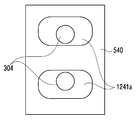
- the electronic device 300 includes a front plate 420, a display 430 disposed under the front plate 420, a sensor 304 disposed under the display 430, and Alternatively, a protective sheet 540 disposed between the sensor 304 and the display 430 and in contact with the surface of the display 430 may be included.
- the front plate 420 protects the display 430 and transmits light emitted from the pixels of the display 430 to the outside, thereby transmitting information displayed on the display 430 to the outside (eg, a user).
- the front plate 420 may be formed of a transparent material, and may be formed of a polymer material, a transparent plastic or glass material.
- the front plate 420 may have a hardness sufficient to protect the display 430.
- the display 430 may include a display module and a polarizing layer disposed on the display module.
- the display 430 may include a panel formed on a display substrate.
- the display panel may include a light emitting layer forming a plurality of pixels and a thin film transistor (TFT) for controlling light of each pixel.
- TFT thin film transistor
- the display 430 through the control of the TFT, light generated from each of the pixels may pass through the polarizing layer and the front plate 420 to be transmitted to the outside of the electronic device 300.
- the polarizing layer may convert transmitted light into linearly polarized light, and may pass through the phase delay layer to convert it into circularly polarized light.
- the electronic device 300 may include a protective sheet 540 disposed under the display 430.
- the protective sheet 540 may include a light blocking layer (eg, a black layer including a bumpy pattern) or a buffer layer (eg, a sponge layer).
- the protective sheet 540 may include an opening 541 corresponding to the sensor 304 disposed under the panel.
- the opening 541 may be a path for light or a signal transmitted to the sensor 304.
- A-A' of FIG. 5A is parallel to the short edge of the side of the housing (eg, the housing 310 of FIG. 3A) (eg, the side 310c of FIG. 3A) and transverses the area where the sensor 304 is disposed.
- B-B' of FIG. 5A is parallel to the long edge of the side of the housing and can cross the area where the sensor is disposed.
- the sensor 304 may include a base 504a and a body portion 504b.
- the base 504a may include components of the sensor 304 and may support the body portion 504b.
- the body portion 504b may include a window (not shown) in a direction toward the opening 541.
- the first width dw of the opening 541 of the protective sheet 540 may be longer than the width of the body portion 504b of the sensor 304.
- the second width dl of the opening 541 of the protective sheet 540 is longer than the width of the main body 504b of the sensor 304. I can.
- the body portion 504b may be included in the opening 541.
- the base 504a may overlap the opening 541 in some areas.
- a ratio obtained by dividing the first width dw by the width of the sensor 304 may be greater than a ratio obtained by dividing the second width dl by the width of the sensor 304.
- the first width dw may be greater than the second width dl.
- the difference between the second width dl and the width of the sensor 304 may be smaller than the width of the sensor 304, but the first width dw and The difference in the width of the sensor 304 may be greater than the width of the sensor 304.
- the opening 541 may be a symmetrically or asymmetrically enlarged shape from the shape of the sensor 304, but the enlargement ratio is large in the first width (dw) direction, but the second width ( The enlargement ratio may be small in the direction of dl).
- FIG. 6 is a view showing the arrangement of the protective sheet and the sensor in the area A of FIG. 3A.
- the sensor 304 may include a first sensor 304a and a second sensor 304b.
- the protective sheet 540 may include a first opening 541a corresponding to the first sensor 304a and may include a second opening 541b corresponding to the second sensor 304b.
- a first sensor may be disposed in the first opening 541a, and a second sensor 304b may be included in the second opening 541b.
- the first sensor 304a and the second sensor 304b may be disposed to be spaced apart from each other, and the first opening 541a and the second opening 541b may be disposed to be spaced apart from each other.
- the first opening 541a and the second opening 541b may be spaced apart to prevent interference or crosstalk of signals or light transmitted or received by the first sensor 304a and the second sensor 304b.
- the first sensor 304a has a long side of the housing (eg, the housing 310 of FIG. 3A) (eg, the side surface 310c of FIG. 3A) within the first opening 541a. It may be arranged to be spaced apart by a first distance d1 in a direction parallel to the corner. The first sensor 304a may be spaced apart by a second distance d2 in a direction parallel to the short edge of the side surface of the housing inside the first opening. As an embodiment, the first sensor 304a may be asymmetrically spaced from both sides in a direction parallel to the side surface of the housing inside the first opening.
- the first sensor 304a may be symmetrically spaced from both sides in a direction parallel to the side surface of the housing inside the first opening.
- the size of the first opening 541a may be formed to a size capable of securing an amount of light required for the sensor.
- the second sensor 304b may be disposed inside the second opening 541b at a position corresponding to the first distance d1 and the second distance d2, like the first sensor. .
- the first opening 541a and the second opening 541b may be spaced apart by a third distance d3.
- the first distance d1 may minimize the distance in order to prevent crosstalk between the first sensor 304a and the second sensor 304b.
- the second distance d2 may be determined in consideration of a sufficient amount of light to secure the performance of the sensor.
- the second distance d2 may be determined in consideration of a tolerance in a manufacturing process. Tolerances in the manufacturing process may be caused by equipment tolerances, outer tolerances, tolerances occurring during the formation of openings, panel align mark tolerances, or tilt tolerances of the protective sheet. The opening and the sensor may overlap due to the tilt tolerance. In order to prevent this, the second distance d2 may be longer than the first distance d1.
- the senor 304 may be a sensor including a light emitting unit and a light receiving unit such as a proximity sensor, a camera, a Time of Flight (ToF) sensor, or an IR sensor.
- a proximity sensor such as a camera, a Time of Flight (ToF) sensor, or an IR sensor.
- the first sensor 304a or the second sensor 304b may be a light emitting sensor or a light receiving sensor.
- a light-shielding area is maintained, thereby preventing sensor recognition failure.
- a third distance d3 between the first opening 541a and the second opening 541b may be secured.
- FIGS. 8A and 8B are diagrams illustrating a position of an opening based on a sensor.
- the electronic device 300 may include a display 430, a front plate 420, or a protective sheet 540.
- the protective sheet 540 may include an opening 541 for a sensor corresponding to the position of the sensor and an opening 542 for a camera corresponding to the position of the camera.
- the display 430 is a flexible printed circuit board 431 connected to a display drive integrate circuit (DDI) at one corner, or a chip-on film (COF). on film).
- An edge at which the flexible printed circuit board or chip-on film (COF) and the display 430 are coupled may be substantially parallel to a short edge of the housing (eg, the housing 310 of FIG. 3A ).
- the protective sheet 540 includes a first alignment mark 491 at one corner, and the protective sheet 431 is provided on the flexible printed circuit board 431.
- a second alignment mark 492 may be included at a corner corresponding to one corner of 540.
- a first alignment mark 491 and a second alignment mark 492 may be used for alignment of the display 430 and the protective sheet 540.
- the second alignment mark 492 may be disposed at a designated position based on the first alignment mark 491 displayed on the display 430.
- the front plate 420, the display 430, and the protective sheet 540 may be aligned.
- the protective sheet 540 and the display 430 include a first alignment mark 491 and a second alignment mark 492 that are the criteria for alignment at one corner, so that the other side facing one corner where the alignment mark is displayed.
- the sensor opening 541 corresponding to the position of the sensor as it goes toward the corner may increase a tolerance in a direction in which one corner extends. For example, if the angle error generated by the assembly of the display 430 and the protective sheet 540 is ⁇ , and the distance to the sensor opening 541 is l, the position where the sensor opening 541 is to be placed and the actual arrangement The distance error (lt) from the location may be l X ⁇ . Since the distance error lt is proportional to the distance l from one corner to the sensor opening 541, the tolerance due to rotation may increase as the distance between the sensor opening 541 is displayed at the corner where the alignment mark is displayed. . When the sensor opening 541 overlaps the sensor, the sensor may be covered by the protective sheet, so the shape of the sensor opening 541 may be formed to have a long length in the direction in which one edge of the alignment mark is displayed. have.
- the position 941b of the actually disposed sensor opening may be moved by lt in the rotation direction 901 than the designed position 941a of the sensor opening.
- the edge of the sensor opening 541 may overlap with the sensor 304, and the recognition distance of the sensor 304 may be shortened, and the amount of a signal emitted or received to the outside may be reduced or distorted. .
- the sensor opening 541 may have the same shape as the first opening 541a or the second opening 541b of FIG. 6.
- the sensor opening 541 may have a long width of an opening parallel to one edge of the protective sheet 540 in which the first alignment mark 591 or the second alignment mark 592 is located.
- the shape of the opening may be different from the shape of the sensor 304. If the width of the opening in the rotating direction 901 is wide, even if it moves from the designed sensor opening position 942a to the actual sensor opening 541 position 942b, the edge of the sensor opening 541 It is possible to prevent the overlap of the sensor 304.
- the electronic device 1000 (eg, the electronic device 101) may be a flexible electronic device.
- the display 1001 may be disposed in a space formed by the first housing structure 1510, the second housing structure 1520, and the hinge cover 1530.
- the display 1001 is formed of a soft material, and can be converted from an open state to a folded state by a hinge structure disposed inside the hinge cover 1530.
- the display 1001 may be formed to be supported by a bracket.
- the bracket may be wrapped by the first housing structure 1510 and the second housing structure 1520.
- the display 1001 may be switched from an unfolded state to a folded state in an in-folding manner by a hinge structure disposed inside the hinge cover 1530.
- the dispreel 1001 may be converted from an unfolded state to a folded state in an out-folding manner by a hinge structure disposed inside the hinge cover 1530.
- the display 1001 may include a first surface 1001a and a second surface 1001b opposite to the first surface 1001a, and the display 1001 includes a plurality of layers stacked thereon. Can be formed. As shown in FIG. 9A, when the electronic device 1000 is in the unfolded state, layers constituting the display 1001 may not be deformed. For example, the side surfaces of the layer forming the first surface 1001a and the layer forming the second surface 1001b may coincide.
- layers constituting the display 1001 may be deformed.
- each of the plurality of layers of the display 1001 may slip.
- a plurality of layers facing from the second surface 1001b to the first surface 1001a may slip.
- the slip direction 1000A of the plurality of layers forming the display 1001 may occur in a direction perpendicular to the folding axis (A axis) on the surface of the display 1001.
- a layer forming the first surface 1001a among the plurality of layers forming the display 1001 may have a greater curvature of the folding area than other layers in a folded state.
- the layer forming the first surface 1001a among the plurality of layers forming the display 1001 has a short radius of curvature, and thus the length of the arc forming the folding area 1103 may be formed to be small.
- a length perpendicular to the folding axis (A axis) of the layer forming the first surface 1001a in the first region 1101 and the second region 1102 extending from the folding region 1103 is the display 1001. It can be longer than other layers forming.
- the layer forming the second surface 1001b may have a smaller curvature than the other layers in the folded state.
- the layer forming the second surface 1001b among the plurality of layers forming the display 1001 has a long radius of curvature, and thus the length of the arc forming the folding area 1103 may be formed to be large.
- the length in the direction perpendicular to the folding axis (A axis) of the layer forming the second surface 1001b in the first area 1101 and the second area 1102 extending from the folding area 1103 is the display 1001. It may be shorter than other layers forming.
- a plurality of layers forming the display 1001 are formed in different lengths of arcs formed in the folding area 1103, so that they are formed on the folding axis in the first area 1101 and the second area 102.
- the length in the vertical direction may be different. Since the layers forming the first region 1101 and the second region 1102 have different lengths, slip may occur in a direction perpendicular to the folding axis (A-axis).
- FIGS. 10A and 10B are diagrams illustrating a position of an opening with respect to a sensor in an open or folded state of an electronic device according to an exemplary embodiment.
- the position 941b of the actually arranged sensor opening may be moved by the slip distance in the slip direction 1100a rather than the designed position 941a of the sensor opening.
- the edge of the sensor opening 541 may overlap with the sensor 304, the recognition distance of the sensor may be shortened, and the amount of a signal emitted or received to the outside may be reduced or distorted.
- the sensor opening may have the same shape as the first opening 541a or the second opening 541b of FIG. 6.
- the sensor opening may have a long width of the opening formed in the slip direction 1100a of the flexible display.
- the shape of the opening may be different from the shape of the sensor 304.
- the width of the corresponding opening in the slip direction 1100a is wide, even if it moves from the designed sensor opening position 1142a to the actual sensor opening position 1142b, the first opening 541a or the second opening It is possible to prevent overlapping of the edge of 541b and the sensor 304.
- the shape of the sensor opening when a shear behavior occurs in layers formed on the display 430 or the sensor 304, in consideration of an error caused by the shear behavior, the shape of the sensor opening and You can decide the size.
- 11, 12, 13, and 14 are diagrams illustrating openings and sensor shapes of a protective sheet according to various embodiments.
- the sensor 304 may include a first sensor (eg, the first sensor 304a of FIG. 6) and a second sensor (eg, the second sensor 304b of FIG. 6 ).
- the sensor 304 may be a sensor module including a light emitting unit and a light receiving unit, such as a proximity sensor.
- the shape of the opening 1241a corresponding to the sensor 304 may be the same as or similar to the shape of the opening of FIG. 6, and there may be a difference in the position of the sensor 304.
- the protective sheet 540 may include a light-shielding area of the light-emitting unit and the light-receiving unit in order to prevent sensor failure.
- the size of the opening 1241a may be larger than that of the sensor 304 in order to prevent the sensor from being covered by the slip. . If the size of the opening 1241a is increased to have the same shape as the sensor 304, unnecessary noise due to signals or light introduced from the outside increases, and thus the sensing performance of the sensor may be deteriorated.
- the sensing performance of the sensor may be deteriorated.
- the width of the opening 1241a in a direction facing the light-emitting portion and the light-receiving portion may be formed to be narrow.
- the senor 304 in the opening 1241a may be formed adjacent to the edge or edge of the opening close to another sensor.
- the position of the sensor 304 can be fixed and the light-shielding area between the light-emitting portion and the light-receiving portion can be enlarged.
- the light-shielding area is enlarged, a light-shielding area is sufficiently secured between the light-emitting unit and the light-receiving unit, thereby reducing a sensor failure rate due to interference of external signals.
- the light emitting part and the light receiving part of the sensor 304 may be arranged to correspond to the rotation direction of the protective sheet 540 or to the slip direction of the layer constituting the display. Slip may occur in the vertical direction.
- the opening 1241b in which the sensor 304 is disposed is an enlarged shape of the opening 1241b than the shape of the sensor 304 in order to prevent the obstruction due to the tilt tolerance of the protective sheet 540 or the slip of the layer.
- the shape of the opening 1341 in the protective sheet 540 may be determined in consideration of the tilt tolerance and the slip distance. .
- slip may occur in the vertical direction.
- the sensor 1490 may have a polygonal shape.
- the opening 1441 may be spaced apart from the sensor 1490 by a first distance d1 in a direction in which slip of the display does not occur or tilt tolerance hardly occurs.
- the opening 1441 may be spaced apart from the sensor 1490 by a second distance d2 in a direction in which slip of the display occurs or a direction in which a tilt tolerance occurs.
- the ratio of the first distance (d1) between the opening (1441) and the sensor (1490) and the first width (dw1) of the sensor in the direction in which the tilt tolerance hardly occurs or the slip does not occur is the slip or tilt tolerance. It may be smaller than a ratio of the second distance d2 between the opening 1441 and the sensor 1490 in the direction in which is generated and the second width dw2 of the sensor.
- the number of lines forming the exterior may be the same, but the enlarged ratio of the opening may be formed in a different shape.
- the protective sheet 540 is formed with a tilt tolerance or a slip of a layer forming the display. It is possible to prevent the sensor 1490 from being covered by the outer edge of the opening 1441.
- the opening of the protective sheet disposed under the display has a shape different from that of the sensor. Can be produced.
- the shape of the opening can widen the width of the opening where the influence of the manufacturing tolerance is large.
- the opening may have a long width in a direction parallel to an edge where an alignment mark indicated for assembly of the electronic device is located. Even if an error occurs in the opening by the tolerance, the edge of the opening and the sensor are not overlapped with each other, thereby ensuring sensor performance.
- An electronic device includes a housing including a first surface and a second surface facing the first surface to form a space (eg, the housing 310 of FIG. 3A ), disposed in the space, and A sensor module (eg, the sensor module 304 of FIG. 3A) including a first sensor (eg, the first sensor 304a of FIG. 6) facing the first surface, and a display disposed on the sensor module (eg: The display 430 of FIG. 4 and a first opening disposed on one surface of the display and having a shape different from the shape of the first sensor at a position corresponding to the first sensor of the sensor module (eg, It may include a protective sheet (for example, the protective sheet 540 of FIG. 5B) forming the opening 541 or the first opening 541a of FIG. 6.
- a protective sheet for example, the protective sheet 540 of FIG. 5B
- the housing includes two long edges facing each other and two short edges facing each other, and the first opening has a first width in a direction parallel to the short edge (for example, in FIG.
- the first width dw) may be different from the second width in a direction parallel to the long edge (eg, the second width dl in FIG. 5C).
- the first One width may be formed longer than the second width
- the ratio of the first width based on the width of the first sensor corresponding to the first width is greater than the ratio of the second width based on the width of the first sensor corresponding to the second width. It can be big.
- the sensor module may include a second sensor
- the protective sheet may further include a second opening corresponding to the second sensor
- the first opening and the second opening may be spaced apart from each other.
- the first sensor may be a light emitting unit
- the second sensor may be a light receiving unit
- the first sensor may be disposed to be skewed at a partial edge of the first opening.
- the sensor module when viewed from the outside, may be covered by the display.
- the display may be a foldable display having a folding axis (eg, a folding axis A of FIG. 9A ).
- the first opening has a first width perpendicular to the folding axis and a second width parallel to the folding axis different from each other, and the first width is a slip distance of the display and the first sensor. Can be greater than the sum of the widths of.
- An electronic device includes a housing including a first surface and a second surface facing the first surface to form a space (eg, the housing 310 of FIG. 3A ), disposed in the space, and A sensor module (eg, the sensor 304 of FIG. 3A) including a first sensor facing a first surface (eg, the first sensor 304a of FIG. 6), a display disposed on the sensor module, and the display A display driving circuit electrically connected, and a first opening disposed between the sensor module and the display and including a region overlapping the sensor module at a position corresponding to the first sensor of the sensor module (eg, FIG. And a protective sheet forming the opening 541 of FIG. 5B or the first opening 541a of FIG.
- the display driving circuit eg, display driver IC 230 of FIG. 2
- the display driving circuit is disposed in the first opening
- a first width in a direction parallel to the edge of the display eg, a first width dw in FIG. 5B
- a second width in a direction perpendicular to the edge of the display on which the display driving circuit is disposed eg, the first width in FIG. 2 width dl
- the first width may be greater than the second width.
- the ratio of the first width based on the width of the first sensor parallel to the first width is the second width based on the width of the first sensor parallel to the second width. May be greater than the ratio.
- the sensor module may include a second sensor
- the protective sheet may include a second opening (eg, the second opening 541b of FIG. 6) corresponding to the second sensor.
- the first opening and the second opening may be spaced apart from each other.
- the first sensor is disposed adjacent to a corner of the first opening close to the second sensor
- the second sensor is disposed adjacent to a corner of the second opening close to the first sensor Can be.
- the first sensor may be a light emitting unit
- the second sensor may be a light receiving unit
- the sensor module when viewed from the outside, may be covered by the display.
- An electronic device includes a housing including a first surface and a second surface facing the first surface to form a space (eg, the housing 310 of FIG. 3A ), disposed in the space, and A sensor facing the first side (e.g., sensor 304 in Fig. 3A), a display disposed on the sensor and including a first alignment mark for placement, and disposed between the sensor and the display And, a first opening including a second alignment mark corresponding to the first alignment mark, and including a region overlapping with the sensor at a position corresponding to the sensor (for example, the opening 541 of FIG. 5B or FIG. 6 ). And a protective sheet (for example, the protective sheet 540 of FIG.
- first opening 541a of the display forming a first opening 541a of the display, wherein the first opening is in a direction parallel to a corner where the first alignment mark is located. It has a first width (eg, a first width (dw) in FIG. 5B) and a second width in a vertical direction (eg, a second width (dl) in FIG. 5C) at a corner where the first alignment mark is located, and the The first width may be larger than the second width.
- the ratio of the first width based on the width of the sensor parallel to the first width may be greater than the ratio of the second width based on the width of the sensor parallel to the second width.
Abstract
An electronic device is disclosed. An electronic device according to various embodiments comprises: a housing including a first surface and a second surface facing the first surface and forming a space; a sensor module arranged in the space and facing the first surface; a display arranged on the sensor module; and a protection sheet arranged on one surface of the display and forming a first opening having a shape different from that of a first sensor at a location of the sensor module, corresponding to that of the first sensor.
Description
다양한 실시예는 센서와 상이한 형상의 개구를 구비하는 디스플레이를 포함하는 전자 장치에 관한 것이다.Various embodiments relate to an electronic device including a display having an opening of a different shape than the sensor.
전자 장치는 복수의 층으로 형성된 디스플레이를 포함할 수 있다. 디스플레이의 하부에 배치되는 센서는 센서와 디스플레이 사이에 보호층을 포함할 수 있다. 보호층은 센서에서 발신하거나 수신하는 신호가 통과하는 통로를 확보하기 위해 개구를 포함할 수 있다. The electronic device may include a display formed of a plurality of layers. The sensor disposed under the display may include a protective layer between the sensor and the display. The protective layer may include an opening to secure a path through which signals transmitted or received by the sensor pass.
기술의 발전에 따라 전자 장치의 전면을 통하여 전달되는 화면의 표시되는 영역의 비율을 높이고자, 베젤에 배치되는 센서들 대신, 디스플레이의 하부에 배치되는 센서에 대한 요구가 증가하고 있다.With the development of technology, in order to increase the ratio of the displayed area of the screen transmitted through the front of the electronic device, there is an increasing demand for sensors disposed under the display instead of sensors disposed on the bezel.
복수의 층을 적층하는 공정을 통해 형성되는 디스플레이는 각각의 층으로부터 발생하는 제작공차가 발생할 수 있으며, 통로에 해당하는 개구의 위치가 변형될 수 있다. 또한, 플렉서블 디스플레이의 경우, 제작 공차외에 복수의 층으로 형성된 디스플레이의 층간 슬립으로 개구의 위치가 변형될 수 있다.In a display formed through a process of stacking a plurality of layers, manufacturing tolerances generated from each layer may occur, and a position of an opening corresponding to a passage may be changed. In addition, in the case of a flexible display, the position of the opening may be changed due to interlayer slip of a display formed of a plurality of layers in addition to manufacturing tolerances.
개구의 위치가 변경되는 경우, 개구의 가장자리 영역은 센서와 중첩될 수 있어, 센서의 성능을 저하시킬 수 있는 우려가 존재한다. 상술한 우려를 해소할 수 있는 방안(solution)이 요구된다.When the position of the opening is changed, the edge region of the opening may overlap with the sensor, and there is a concern that performance of the sensor may be deteriorated. There is a need for a solution to alleviate the above concerns.
다양한 실시예에 따르는 전자 장치는, 제1 면 및 상기 제1 면을 마주보며 공간을 형성하는 제2 면을 포함하는 하우징, 상기 제2 면 상에 배치되고, 제1 센서를 포함하는 센서 모듈, 상기 센서 모듈상에 배치되는 디스플레이와, 상기 센서 모듈과 상기 디스플레이 사이에 배치되고, 상기 센서 모듈의 적어도 하나의 센서에 대응되는 위치에서 상기 센서의 형상과 상이한 형상의 제1 개구를 형성하는 보호 시트를 포함할 수 있다.An electronic device according to various embodiments includes a housing including a first surface and a second surface facing the first surface to form a space, a sensor module disposed on the second surface and including a first sensor, A display disposed on the sensor module, and a protective sheet disposed between the sensor module and the display, and forming a first opening having a shape different from that of the sensor at a position corresponding to at least one sensor of the sensor module It may include.
다양한 실시예에 따르는 전자 장치는, 제1 면 및 상기 제1 면을 마주보며 공간을 형성하는 제2 면을 포함하는 하우징, 상기 제2 면 상에 배치되고, 제1 센서를 포함하는 센서 모듈, 상기 센서 모듈상에 배치되는 디스플레이, 상기 디스플레이와 전기적으로 연결되는 디스플레이 구동 회로와, 상기 센서 모듈과 상기 디스플레이 사이에 배치되고, 상기 센서 모듈의 제1 센서에 대응되는 위치에서 상기 센서 모듈과 중첩되는 영역을 포함하는 제1 개구를 형성하는 보호 시트를 포함하고, 상기 제1 개구는 상기 디스플레이 구동 회로가 배치되는 디스플레이의 모서리에 평행한 방향의 제1 너비와 상기 디스플레이 구동 회로가 배치되는 디스플레이의 모서리에 수직 방향의 제2 너비를 가지고, 상기 제1 너비는 상기 제2 너비보다 클 수 있다.An electronic device according to various embodiments includes a housing including a first surface and a second surface facing the first surface to form a space, a sensor module disposed on the second surface and including a first sensor, A display disposed on the sensor module, a display driving circuit electrically connected to the display, and disposed between the sensor module and the display, and overlapping the sensor module at a position corresponding to the first sensor of the sensor module And a protective sheet forming a first opening including an area, wherein the first opening has a first width in a direction parallel to an edge of a display on which the display driving circuit is disposed and an edge of a display on which the display driving circuit is disposed It has a second width in the vertical direction to, and the first width may be greater than the second width.
다양한 실시예에 따르는 전자 장치는, 제1 면 및 상기 제1 면을 마주보며 공간을 형성하는 제2 면을 포함하는 하우징, 상기 제2 면 상에 배치되고, 제1 센서를 포함하는 센서 모듈, 상기 센서 모듈상에 배치되고, 배치를 위한 제1 정렬 표식(align mark)를 포함하는 디스플레이와, 상기 센서 모듈과 상기 디스플레이 사이에 배치되고, 상기 제1 표식에 대응되는 제2 표식을 포함하고, 상기 센서 모듈의 제1 센서에 대응되는 위치에서 상기 센서 모듈과 중첩되는 영역을 포함하는 제1 개구를 형성하는 보호 시트를 포함하고, 상기 제1 개구는 상기 디스플레이 상기 제2 표식이 위치하는 모서리에 평행한 방향의 제1 너비 및 상기 제2 표식이 위치하는 모서리에 수직 방향의 제2 너비를 가지고, 상기 제1 너비는 상기 제2 너비보다 클 수 있다.An electronic device according to various embodiments includes a housing including a first surface and a second surface facing the first surface to form a space, a sensor module disposed on the second surface and including a first sensor, A display disposed on the sensor module and including a first alignment mark for placement, and a second mark disposed between the sensor module and the display and corresponding to the first mark, And a protective sheet forming a first opening including an area overlapping with the sensor module at a position corresponding to the first sensor of the sensor module, and the first opening is at a corner where the display second mark is located A first width in a parallel direction and a second width in a vertical direction to a corner where the second mark is located, and the first width may be greater than the second width.
다양한 실시예에 따르는 전자 장치는, 배면 센서의 형상과 다른 개구를 형성한 보호 시트를 포함하여, 개구의 가장자리가 배면 센서와 중첩되는 것을 방지할 수 있다. 배면 센서와 개구의 가장자리의 중첩이 일어나지 않아, 전자 장치는 센서의 가림 현상을 줄일 수 있다. 전자 장치는, 개구의 너비를 상이하게 형성하여, 전자 장치 제조 공정상에 발생하는 공차에 의한 가림현상을 방지할 수 있다.An electronic device according to various embodiments of the present disclosure may include a protective sheet having an opening different from that of the rear sensor, and may prevent an edge of the opening from overlapping with the rear sensor. Since the rear sensor and the edge of the opening do not overlap, the electronic device can reduce the occlusion of the sensor. In the electronic device, by forming different widths of the openings, it is possible to prevent a phenomenon of being blocked by tolerances occurring in the electronic device manufacturing process.
다양한 실시예에 따르는 전자 장치는, 개구 영역의 최소화를 통하여 간섭에 의한 센서 성능 저하를 방지할 수 있다.The electronic device according to various embodiments may prevent degradation of sensor performance due to interference by minimizing the opening area.
도 1은, 다양한 실시예들에 따른, 네트워크 환경(100) 내의 전자 장치(101)의 블럭도이다.1 is a block diagram of an electronic device 101 in a network environment 100 according to various embodiments.
도 2는 다양한 실시예들에 따른, 표시 장치(160)의 블록도(200)이다. 2 is a block diagram 200 of a display device 160 according to various embodiments.
도 3a는 일 실시예에 따른 전자 장치의 전면의 사시도이다. 3A is a front perspective view of an electronic device according to an exemplary embodiment.
도 3b는 도 3a의 전자 장치의 후면의 사시도이다.3B is a perspective view of the rear side of the electronic device of FIG. 3A.
도 4는 도 3a의 전자 장치의 분해 사시도이다.4 is an exploded perspective view of the electronic device of FIG. 3A.
도 5a는 도 3a의 A 영역을 확대한 도면이다.5A is an enlarged view of area A of FIG. 3A.
도 5b는 도 5a의 A-A'의 단면을 도시한 단면도이고, 도 5c는 도 5a의 B-B'의 단면을 도시한 단면도이다.5B is a cross-sectional view showing a cross-section taken along line A-A' of FIG. 5A, and FIG. 5C is a cross-sectional view showing a cross-section taken along line A-A' in FIG.
도 6은 도 3a의 A 영역에서의 보호시트와 센서의 배치를 도시한 도면이다.6 is a view showing the arrangement of the protective sheet and the sensor in the area A of FIG. 3A.
도 7a 및 도 7b는 다양한 실시예에 따른, 보호시트의 배치를 도시한 도면이다.7A and 7B are diagrams illustrating an arrangement of a protective sheet according to various embodiments.
도 8a 및 도 8b는 센서를 기준으로 개구의 위치를 나타내는 도면이다.8A and 8B are views showing the position of the opening with respect to the sensor.
도 9a는 일 실시 예에 따른 전자 장치의 펼침 상태에서의 디스플레이 층을 나타낸다.9A illustrates a display layer in an unfolded state of an electronic device according to an exemplary embodiment.
도 9b는 일 실시예에 따른 전자 장치의 접힘 상태에서의 슬립이 발생한 디스플레이의 층을 나타낸다.9B illustrates a layer of a display in which slip occurs in a folded state of an electronic device according to an exemplary embodiment.
도 10a 및 도 10b는 일 실시예에 따른 전자 장치의 펼침 상태 또는 접힘 상태에서 센서를 기준으로 개구의 위치를 나타내는 도면이다.10A and 10B are diagrams illustrating a position of an opening with respect to a sensor in an open or folded state of an electronic device according to an exemplary embodiment.
도 11, 12, 13 및 14는 다양한 실시예에 따르는 보호시트의 개구 및 센서 형상을 도시한 도면이다.11, 12, 13, and 14 are diagrams illustrating openings and sensor shapes of a protective sheet according to various embodiments.
도 1은, 다양한 실시예들에 따른, 네트워크 환경(100) 내의 전자 장치(101)의 블럭도이다. 도 1을 참조하면, 네트워크 환경(100)에서 전자 장치(101)는 제 1 네트워크(198)(예: 근거리 무선 통신 네트워크)를 통하여 전자 장치(102)와 통신하거나, 또는 제 2 네트워크(199)(예: 원거리 무선 통신 네트워크)를 통하여 전자 장치(104) 또는 서버(108)와 통신할 수 있다. 일실시예에 따르면, 전자 장치(101)는 서버(108)를 통하여 전자 장치(104)와 통신할 수 있다. 일실시예에 따르면, 전자 장치(101)는 프로세서(120), 메모리(130), 입력 장치(150), 음향 출력 장치(155), 표시 장치(160), 오디오 모듈(170), 센서 모듈(176), 인터페이스(177), 햅틱 모듈(179), 카메라 모듈(180), 전력 관리 모듈(188), 배터리(189), 통신 모듈(190), 가입자 식별 모듈(196), 또는 안테나 모듈(197)을 포함할 수 있다. 어떤 실시예에서는, 전자 장치(101)에는, 이 구성요소들 중 적어도 하나(예: 표시 장치(160) 또는 카메라 모듈(180))가 생략되거나, 하나 이상의 다른 구성 요소가 추가될 수 있다. 어떤 실시예에서는, 이 구성요소들 중 일부들은 하나의 통합된 회로로 구현될 수 있다. 예를 들면, 센서 모듈(176)(예: 지문 센서, 홍채 센서, 또는 조도 센서)은 표시 장치(160)(예: 디스플레이)에 임베디드된 채 구현될 수 있다1 is a block diagram of an electronic device 101 in a network environment 100 according to various embodiments. Referring to FIG. 1, in a network environment 100, the electronic device 101 communicates with the electronic device 102 through a first network 198 (for example, a short-range wireless communication network), or a second network 199 It is possible to communicate with the electronic device 104 or the server 108 through (eg, a long-distance wireless communication network). According to an embodiment, the electronic device 101 may communicate with the electronic device 104 through the server 108. According to an embodiment, the electronic device 101 includes a processor 120, a memory 130, an input device 150, an audio output device 155, a display device 160, an audio module 170, and a sensor module ( 176, interface 177, haptic module 179, camera module 180, power management module 188, battery 189, communication module 190, subscriber identification module 196, or antenna module 197 ) Can be included. In some embodiments, at least one of these components (eg, the display device 160 or the camera module 180) may be omitted or one or more other components may be added to the electronic device 101. In some embodiments, some of these components may be implemented as one integrated circuit. For example, the sensor module 176 (eg, a fingerprint sensor, an iris sensor, or an illuminance sensor) may be implemented while being embedded in the display device 160 (eg, a display).
프로세서(120)는, 예를 들면, 소프트웨어(예: 프로그램(140))를 실행하여 프로세서(120)에 연결된 전자 장치(101)의 적어도 하나의 다른 구성요소(예: 하드웨어 또는 소프트웨어 구성요소)을 제어할 수 있고, 다양한 데이터 처리 또는 연산을 수행할 수 있다. 일실시예에 따르면, 데이터 처리 또는 연산의 적어도 일부로서, 프로세서(120)는 다른 구성요소(예: 센서 모듈(176) 또는 통신 모듈(190))로부터 수신된 명령 또는 데이터를 휘발성 메모리(132)에 로드하고, 휘발성 메모리(132)에 저장된 명령 또는 데이터를 처리하고, 결과 데이터를 비휘발성 메모리(134)에 저장할 수 있다. 일실시예에 따르면, 프로세서(120)는 메인 프로세서(121)(예: 중앙 처리 장치 또는 어플리케이션 프로세서), 및 이와는 독립적으로 또는 함께 운영 가능한 보조 프로세서(123)(예: 그래픽 처리 장치, 이미지 시그널 프로세서, 센서 허브 프로세서, 또는 커뮤니케이션 프로세서)를 포함할 수 있다. 추가적으로 또는 대체적으로, 보조 프로세서(123)은 메인 프로세서(121)보다 저전력을 사용하거나, 또는 지정된 기능에 특화되도록 설정될 수 있다. 보조 프로세서(123)는 메인 프로세서(121)와 별개로, 또는 그 일부로서 구현될 수 있다.The processor 120, for example, executes software (eg, a program 140) to implement at least one other component (eg, a hardware or software component) of the electronic device 101 connected to the processor 120. It can be controlled and can perform various data processing or operations. According to an embodiment, as at least part of data processing or operation, the processor 120 may store commands or data received from other components (eg, the sensor module 176 or the communication module 190) to the volatile memory 132. The command or data stored in the volatile memory 132 may be processed, and result data may be stored in the nonvolatile memory 134. According to an embodiment, the processor 120 includes a main processor 121 (eg, a central processing unit or an application processor), and a secondary processor 123 (eg, a graphic processing unit, an image signal processor) that can be operated independently or together with the main processor 121 (eg, a central processing unit or an application processor). , A sensor hub processor, or a communication processor). Additionally or alternatively, the coprocessor 123 may be set to use less power than the main processor 121 or to be specialized for a designated function. The secondary processor 123 may be implemented separately from the main processor 121 or as a part thereof.
보조 프로세서(123)는, 예를 들면, 메인 프로세서(121)가 인액티브(예: 슬립) 상태에 있는 동안 메인 프로세서(121)를 대신하여, 또는 메인 프로세서(121)가 액티브(예: 어플리케이션 실행) 상태에 있는 동안 메인 프로세서(121)와 함께, 전자 장치(101)의 구성요소들 중 적어도 하나의 구성요소(예: 표시 장치(160), 센서 모듈(176), 또는 통신 모듈(190))와 관련된 기능 또는 상태들의 적어도 일부를 제어할 수 있다. 일실시예에 따르면, 보조 프로세서(123)(예: 이미지 시그널 프로세서 또는 커뮤니케이션 프로세서)는 기능적으로 관련 있는 다른 구성 요소(예: 카메라 모듈(180) 또는 통신 모듈(190))의 일부로서 구현될 수 있다. The coprocessor 123 is, for example, on behalf of the main processor 121 while the main processor 121 is in an inactive (eg, sleep) state, or the main processor 121 is active (eg, an application is executed). ) While in the state, together with the main processor 121, at least one of the components of the electronic device 101 (for example, the display device 160, the sensor module 176, or the communication module 190) It is possible to control at least some of the functions or states related to. According to an embodiment, the coprocessor 123 (eg, an image signal processor or a communication processor) may be implemented as part of another functionally related component (eg, the camera module 180 or the communication module 190). have.
메모리(130)는, 전자 장치(101)의 적어도 하나의 구성요소(예: 프로세서(120) 또는 센서모듈(176))에 의해 사용되는 다양한 데이터를 저장할 수 있다. 데이터는, 예를 들어, 소프트웨어(예: 프로그램(140)) 및, 이와 관련된 명령에 대한 입력 데이터 또는 출력 데이터를 포함할 수 있다. 메모리(130)는, 휘발성 메모리(132) 또는 비휘발성 메모리(134)를 포함할 수 있다. The memory 130 may store various data used by at least one component of the electronic device 101 (eg, the processor 120 or the sensor module 176). The data may include, for example, software (eg, the program 140) and input data or output data for commands related thereto. The memory 130 may include a volatile memory 132 or a nonvolatile memory 134.
프로그램(140)은 메모리(130)에 소프트웨어로서 저장될 수 있으며, 예를 들면, 운영 체제(142), 미들 웨어(144) 또는 어플리케이션(146)을 포함할 수 있다. The program 140 may be stored as software in the memory 130, and may include, for example, an operating system 142, middleware 144, or an application 146.
입력 장치(150)는, 전자 장치(101)의 구성요소(예: 프로세서(120))에 사용될 명령 또는 데이터를 전자 장치(101)의 외부(예: 사용자)로부터 수신할 수 있다. 입력 장치(150)은, 예를 들면, 마이크, 마우스, 키보드 또는 디지털 펜(예:스타일러스 펜)을 포함할 수 있다. The input device 150 may receive a command or data to be used for a component of the electronic device 101 (eg, the processor 120) from an outside (eg, a user) of the electronic device 101. The input device 150 may include, for example, a microphone, a mouse, a keyboard, or a digital pen (eg, a stylus pen).
음향 출력 장치(155)는 음향 신호를 전자 장치(101)의 외부로 출력할 수 있다. 음향 출력 장치(155)는, 예를 들면, 스피커 또는 리시버를 포함할 수 있다. 스피커는 멀티미디어 재생 또는 녹음 재생과 같이 일반적인 용도로 사용될 수 있고, 리시버는 착신 전화를 수신하기 위해 사용될 수 있다. 일실시예에 따르면, 리시버는 스피커와 별개로, 또는 그 일부로서 구현될 수 있다.The sound output device 155 may output an sound signal to the outside of the electronic device 101. The sound output device 155 may include, for example, a speaker or a receiver. The speaker can be used for general purposes such as multimedia playback or recording playback, and the receiver can be used to receive incoming calls. According to one embodiment, the receiver may be implemented separately from the speaker or as part of it.
표시 장치(160)는 전자 장치(101)의 외부(예: 사용자)로 정보를 시각적으로 제공할 수 있다. 표시 장치(160)은, 예를 들면, 디스플레이, 홀로그램 장치, 또는 프로젝터 및 해당 장치를 제어하기 위한 제어 회로를 포함할 수 있다. 일실시예에 따르면, 표시 장치(160)는 터치를 감지하도록 설정된 터치 회로(touch circuitry), 또는 상기 터치에 의해 발생되는 힘의 세기를 측정하도록 설정된 센서 회로(예: 압력 센서)를 포함할 수 있다. The display device 160 may visually provide information to the outside of the electronic device 101 (eg, a user). The display device 160 may include, for example, a display, a hologram device, or a projector and a control circuit for controlling the device. According to an embodiment, the display device 160 may include a touch circuitry set to sense a touch, or a sensor circuit (eg, a pressure sensor) set to measure the strength of a force generated by the touch. have.
오디오 모듈(170)은 소리를 전기 신호로 변환시키거나, 반대로 전기 신호를 소리로 변환시킬 수 있다. 일실시예에 따르면, 오디오 모듈(170)은, 입력 장치(150) 를 통해 소리를 획득하거나, 음향 출력 장치(155), 또는 전자 장치(101)와 직접 또는 무선으로 연결된 외부 전자 장치(예: 전자 장치(102)) (예: 스피커 또는 헤드폰))를 통해 소리를 출력할 수 있다.The audio module 170 may convert sound into an electric signal or, conversely, convert an electric signal into sound. According to an embodiment, the audio module 170 acquires sound through the input device 150, the sound output device 155, or an external electronic device (for example, an external electronic device directly or wirelessly connected to the electronic device 101). Sound may be output through the electronic device 102) (for example, a speaker or headphones).
센서 모듈(176)은 전자 장치(101)의 작동 상태(예: 전력 또는 온도), 또는 외부의 환경 상태(예: 사용자 상태)를 감지하고, 감지된 상태에 대응하는 전기 신호 또는 데이터 값을 생성할 수 있다. 일실시예에 따르면, 센서 모듈(176)은, 예를 들면, 제스처 센서, 자이로 센서, 기압 센서, 마그네틱 센서, 가속도 센서, 그립 센서, 근접 센서, 컬러 센서, IR(infrared) 센서, 생체 센서, 온도 센서, 습도 센서, 또는 조도 센서를 포함할 수 있다. The sensor module 176 detects an operating state (eg, power or temperature) of the electronic device 101, or an external environmental state (eg, a user state), and generates an electrical signal or data value corresponding to the detected state. can do. According to an embodiment, the sensor module 176 may include, for example, a gesture sensor, a gyro sensor, an atmospheric pressure sensor, a magnetic sensor, an acceleration sensor, a grip sensor, a proximity sensor, a color sensor, an IR (infrared) sensor, a biometric sensor, It may include a temperature sensor, a humidity sensor, or an illuminance sensor.
인터페이스(177)는 전자 장치(101)이 외부 전자 장치(예: 전자 장치(102))와 직접 또는 무선으로 연결되기 위해 사용될 수 있는 하나 이상의 지정된 프로토콜들을 지원할 수 있다. 일실시예에 따르면, 인터페이스(177)는, 예를 들면, HDMI(high definition multimedia interface), USB(universal serial bus) 인터페이스, SD카드 인터페이스, 또는 오디오 인터페이스를 포함할 수 있다.The interface 177 may support one or more designated protocols that may be used for the electronic device 101 to connect directly or wirelessly with an external electronic device (eg, the electronic device 102 ). According to an embodiment, the interface 177 may include, for example, a high definition multimedia interface (HDMI), a universal serial bus (USB) interface, an SD card interface, or an audio interface.
연결 단자(178)는, 그를 통해서 전자 장치(101)가 외부 전자 장치(예: 전자 장치(102))와 물리적으로 연결될 수 있는 커넥터를 포함할 수 있다. 일실시예에 따르면, 연결 단자(178)은, 예를 들면, HDMI 커넥터, USB 커넥터, SD 카드 커넥터, 또는 오디오 커넥터(예: 헤드폰 커넥터)를 포함할 수 있다.The connection terminal 178 may include a connector through which the electronic device 101 can be physically connected to an external electronic device (eg, the electronic device 102 ). According to an embodiment, the connection terminal 178 may include, for example, an HDMI connector, a USB connector, an SD card connector, or an audio connector (eg, a headphone connector).
햅틱 모듈(179)은 전기적 신호를 사용자가 촉각 또는 운동 감각을 통해서 인지할 수 있는 기계적인 자극(예: 진동 또는 움직임) 또는 전기적인 자극으로 변환할 수 있다. 일실시예에 따르면, 햅틱 모듈(179)은, 예를 들면, 모터, 압전 소자, 또는 전기 자극 장치를 포함할 수 있다.The haptic module 179 may convert an electrical signal into a mechanical stimulus (eg, vibration or movement) or an electrical stimulus that a user can perceive through a tactile or motor sense. According to an embodiment, the haptic module 179 may include, for example, a motor, a piezoelectric element, or an electrical stimulation device.
카메라 모듈(180)은 정지 영상 및 동영상을 촬영할 수 있다. 일실시예에 따르면, 카메라 모듈(180)은 하나 이상의 렌즈들, 이미지 센서들, 이미지 시그널 프로세서들, 또는 플래시들을 포함할 수 있다.The camera module 180 may capture a still image and a video. According to an embodiment, the camera module 180 may include one or more lenses, image sensors, image signal processors, or flashes.
전력 관리 모듈(188)은 전자 장치(101)에 공급되는 전력을 관리할 수 있다. 일실시예에 따르면, 전력 관리 모듈(388)은, 예를 들면, PMIC(power management integrated circuit)의 적어도 일부로서 구현될 수 있다.The power management module 188 may manage power supplied to the electronic device 101. According to an embodiment, the power management module 388 may be implemented as at least a part of, for example, a power management integrated circuit (PMIC).
배터리(189)는 전자 장치(101)의 적어도 하나의 구성 요소에 전력을 공급할 수 있다. 일실시예에 따르면, 배터리(189)는, 예를 들면, 재충전 불가능한 1차 전지, 재충전 가능한 2차 전지 또는 연료 전지를 포함할 수 있다.The battery 189 may supply power to at least one component of the electronic device 101. According to an embodiment, the battery 189 may include, for example, a non-rechargeable primary cell, a rechargeable secondary cell, or a fuel cell.
통신 모듈(190)은 전자 장치(101)와 외부 전자 장치(예: 전자 장치(102), 전자 장치(104), 또는 서버(108))간의 직접(예: 유선) 통신 채널 또는 무선 통신 채널의 수립, 및 수립된 통신 채널을 통한 통신 수행을 지원할 수 있다. 통신 모듈(190)은 프로세서(120)(예: 어플리케이션 프로세서)와 독립적으로 운영되고, 직접(예: 유선) 통신 또는 무선 통신을 지원하는 하나 이상의 커뮤니케이션 프로세서를 포함할 수 있다. 일실시예에 따르면, 통신 모듈(190)은 무선 통신 모듈(192)(예: 셀룰러 통신 모듈, 근거리 무선 통신 모듈, 또는 GNSS(global navigation satellite system) 통신 모듈) 또는 유선 통신 모듈(194)(예: LAN(local area network) 통신 모듈, 또는 전력선 통신 모듈)을 포함할 수 있다. 이들 통신 모듈 중 해당하는 통신 모듈은 제 1 네트워크(198)(예: 블루투스, WiFi direct 또는 IrDA(infrared data association) 같은 근거리 통신 네트워크) 또는 제 2 네트워크(199)(예: 셀룰러 네트워크, 인터넷, 또는 컴퓨터 네트워크(예: LAN 또는 WAN)와 같은 원거리 통신 네트워크)를 통하여 외부 전자 장치와 통신할 수 있다. 이런 여러 종류의 통신 모듈들은 하나의 구성 요소(예: 단일 칩)으로 통합되거나, 또는 서로 별도의 복수의 구성 요소들(예: 복수 칩들)로 구현될 수 있다. 무선 통신 모듈(192)은 가입자 식별 모듈(196)에 저장된 가입자 정보(예: 국제 모바일 가입자 식별자(IMSI))를 이용하여 제 1 네트워크(198) 또는 제 2 네트워크(199)와 같은 통신 네트워크 내에서 전자 장치(101)를 확인 및 인증할 수 있다. The communication module 190 is a direct (eg, wired) communication channel or a wireless communication channel between the electronic device 101 and an external electronic device (eg, electronic device 102, electronic device 104, or server 108). It is possible to support establishment and communication through the established communication channel. The communication module 190 operates independently of the processor 120 (eg, an application processor), and may include one or more communication processors that support direct (eg, wired) communication or wireless communication. According to an embodiment, the communication module 190 is a wireless communication module 192 (eg, a cellular communication module, a short-range wireless communication module, or a global navigation satellite system (GNSS) communication module) or a wired communication module 194 (eg : A LAN (local area network) communication module, or a power line communication module) may be included. Among these communication modules, a corresponding communication module is a first network 198 (for example, a short-range communication network such as Bluetooth, WiFi direct or IrDA (infrared data association)) or a second network 199 (for example, a cellular network, the Internet, or It can communicate with external electronic devices through a computer network (for example, a telecommunication network such as a LAN or WAN). These various types of communication modules may be integrated into one component (eg, a single chip), or may be implemented as a plurality of separate components (eg, multiple chips). The wireless communication module 192 uses subscriber information stored in the subscriber identification module 196 (eg, International Mobile Subscriber Identifier (IMSI)) within a communication network such as the first network 198 or the second network 199. The electronic device 101 can be checked and authenticated.
안테나 모듈(197)은 신호 또는 전력을 외부(예: 외부 전자 장치)로 송신하거나 외부로부터 수신할 수 있다. 일실시예에 따르면, 안테나 모듈은 서브스트레이트(예: PCB) 위에 형성된 도전체 또는 도전성 패턴으로 이루어진 방사체를 포함하는 하나의 안테나를 포함할 수 있다. 일실시예에 따르면, 안테나 모듈(197)은 복수의 안테나들을 포함할 수 있다. 이런 경우, 제 1 네트워크(198) 또는 제 2 네트워크(199)와 같은 통신 네트워크에서 사용되는 통신 방식에 적합한 적어도 하나의 안테나가, 예를 들면, 통신 모듈(190)에 의하여 상기 복수의 안테나들로부터 선택될 수 있다. 신호 또는 전력은 상기 선택된 적어도 하나의 안테나를 통하여 통신 모듈(190)과 외부 전자 장치 간에 송신되거나 수신될 수 있다. 어떤 실시예에 따르면, 방사체 이외에 다른 부품(예: RFIC)이 추가로 안테나 모듈(197)의 일부로 형성될 수 있다.The antenna module 197 may transmit a signal or power to the outside (eg, an external electronic device) or receive from the outside. According to an embodiment, the antenna module may include one antenna including a conductor formed on a substrate (eg, a PCB) or a radiator formed of a conductive pattern. According to an embodiment, the antenna module 197 may include a plurality of antennas. In this case, at least one antenna suitable for a communication method used in a communication network such as the first network 198 or the second network 199 is, for example, provided by the communication module 190 from the plurality of antennas. Can be chosen. The signal or power may be transmitted or received between the communication module 190 and an external electronic device through the at least one selected antenna. According to some embodiments, other components (eg, RFIC) other than the radiator may be additionally formed as part of the antenna module 197.
상기 구성요소들 중 적어도 일부는 주변 기기들간 통신 방식(예: 버스, GPIO(general purpose input and output), SPI(serial peripheral interface), 또는 MIPI(mobile industry processor interface))를 통해 서로 연결되고 신호(예: 명령 또는 데이터)를 상호간에 교환할 수 있다.At least some of the components are connected to each other through a communication method (e.g., bus, general purpose input and output (GPIO), serial peripheral interface (SPI), or mobile industry processor interface (MIPI))) between peripheral devices and signals ( E.g. commands or data) can be exchanged with each other.
일실시예에 따르면, 명령 또는 데이터는 제 2 네트워크(199)에 연결된 서버(108)를 통해서 전자 장치(101)와 외부의 전자 장치(104)간에 송신 또는 수신될 수 있다. 전자 장치(102, 104) 각각은 전자 장치(101)와 동일한 또는 다른 종류의 장치일 수 있다. 일실시예에 따르면, 전자 장치(101)에서 실행되는 동작들의 전부 또는 일부는 외부 전자 장치들(102, 104, or 108) 중 하나 이상의 외부 장치들에서 실행될 수 있다. 예를 들면, 전자 장치(101)가 어떤 기능이나 서비스를 자동으로, 또는 사용자 또는 다른 장치로부터의 요청에 반응하여 수행해야 할 경우에, 전자 장치(101)는 기능 또는 서비스를 자체적으로 실행시키는 대신에 또는 추가적으로, 하나 이상의 외부 전자 장치들에게 그 기능 또는 그 서비스의 적어도 일부를 수행하라고 요청할 수 있다. 상기 요청을 수신한 하나 이상의 외부 전자 장치들은 요청된 기능 또는 서비스의 적어도 일부, 또는 상기 요청과 관련된 추가 기능 또는 서비스를 실행하고, 그 실행의 결과를 전자 장치(101)로 전달할 수 있다. 전자 장치(101)는 상기 결과를, 그대로 또는 추가적으로 처리하여, 상기 요청에 대한 응답의 적어도 일부로서 제공할 수 있다. 이를 위하여, 예를 들면, 클라우드 컴퓨팅, 분산 컴퓨팅, 또는 클라이언트-서버 컴퓨팅 기술이 이용될 수 있다. According to an embodiment, commands or data may be transmitted or received between the electronic device 101 and the external electronic device 104 through the server 108 connected to the second network 199. Each of the electronic devices 102 and 104 may be a device of the same or different type as the electronic device 101. According to an embodiment, all or part of the operations executed by the electronic device 101 may be executed by one or more of the external electronic devices 102, 104, or 108. For example, when the electronic device 101 needs to perform a function or service automatically or in response to a request from a user or another device, the electronic device 101 does not execute the function or service by itself. In addition or in addition, it is possible to request one or more external electronic devices to perform the function or at least part of the service. One or more external electronic devices receiving the request may execute at least a part of the requested function or service, or an additional function or service related to the request, and transmit the execution result to the electronic device 101. The electronic device 101 may process the result as it is or additionally and provide it as at least a part of a response to the request. To this end, for example, cloud computing, distributed computing, or client-server computing technology may be used.
도 2는 다양한 실시예들에 따른, 표시 장치(160)의 블록도(200)이다. 2 is a block diagram 200 of a display device 160 according to various embodiments.
도 2를 참조하면, 표시 장치(160)는 디스플레이(210), 및 이를 제어하기 위한 디스플레이 드라이버 IC(DDI)(230)를 포함할 수 있다. DDI(230)는 인터페이스 모듈(231), 메모리(233)(예: 버퍼 메모리), 이미지 처리 모듈(235), 또는 맵핑 모듈(237)을 포함할 수 있다. DDI(230)은, 예를 들면, 영상 데이터, 또는 상기 영상 데이터를 제어하기 위한 명령에 대응하는 영상 제어 신호를 포함하는 영상 정보를 인터페이스 모듈(231)을 통해 전자 장치 101의 다른 구성요소로부터 수신할 수 있다. 예를 들면, 일실시예에 따르면, 영상 정보는 프로세서(120)(예: 메인 프로세서(121)(예: 어플리케이션 프로세서) 또는 메인 프로세서(121)의 기능과 독립적으로 운영되는 보조 프로세서(123)(예: 그래픽 처리 장치)로부터 수신될 수 있다. DDI(230)는 터치 회로(250) 또는 센서 모듈(176) 등과 상기 인터페이스 모듈(231)을 통하여 커뮤니케이션할 수 있다. 또한, DDI(230)는 상기 수신된 영상 정보 중 적어도 일부를 메모리(233)에, 예를 들면, 프레임 단위로 저장할 수 있다. 이미지 처리 모듈(235)은, 예를 들면, 상기 영상 데이터의 적어도 일부를 상기 영상 데이터의 특성 또는 디스플레이(210)의 특성에 적어도 기반하여 전처리 또는 후처리(예: 해상도, 밝기, 또는 크기 조정)를 수행할 수 있다. 맵핑 모듈(237)은 이미지 처리 모듈(135)를 통해 전처리 또는 후처리된 상기 영상 데이터에 대응하는 전압 값 또는 전류 값을 생성할 수 있다. 일실시예에 따르면, 전압 값 또는 전류 값의 생성은 예를 들면, 디스플레이(210)의 픽셀들의 속성(예: 픽셀들의 배열(RGB stripe 또는 pentile 구조), 또는 서브 픽셀들 각각의 크기)에 적어도 일부 기반하여 수행될 수 있다. 디스플레이(210)의 적어도 일부 픽셀들은, 예를 들면, 상기 전압 값 또는 전류 값에 적어도 일부 기반하여 구동됨으로써 상기 영상 데이터에 대응하는 시각적 정보(예: 텍스트, 이미지, 또는 아이콘)가 디스플레이(210)를 통해 표시될 수 있다.Referring to FIG. 2, the display device 160 may include a display 210 and a display driver IC (DDI) 230 for controlling the display 210. The DDI 230 may include an interface module 231, a memory 233 (eg, a buffer memory), an image processing module 235, or a mapping module 237. The DDI 230 receives, for example, image data or image information including an image control signal corresponding to a command for controlling the image data from other components of the electronic device 101 through the interface module 231. can do. For example, according to an embodiment, the image information is processor 120 (for example, the main processor 121 (for example, an application processor) or a coprocessor 123 that operates independently of the function of the main processor 121) ( Example: It may be received from a graphic processing device) The DDI 230 may communicate with the touch circuit 250 or the sensor module 176 through the interface module 231. In addition, the DDI 230 may be the same. At least a portion of the received image information may be stored in the memory 233, for example, in a frame unit. The image processing module 235 may, for example, store at least a part of the image data as a characteristic of the image data or Pre-processing or post-processing (eg, resolution, brightness, or size adjustment) may be performed based at least on the characteristics of the display 210. The mapping module 237 is preprocessed or post-processed through the image processing module 135. A voltage value or a current value corresponding to the image data may be generated According to an embodiment, generation of a voltage value or a current value may include, for example, a property of pixels of the display 210 (eg, an array of pixels ( RGB stripe or pentile structure), or the size of each of the subpixels). At least some of the pixels of the display 210 are, for example, at least partially based on the voltage value or the current value. By being driven, visual information (eg, text, image, or icon) corresponding to the image data may be displayed through the display 210.
일실시예에 따르면, 표시 장치(160)는 터치 회로(250)를 더 포함할 수 있다. 터치 회로(250)는 터치 센서(251) 및 이를 제어하기 위한 터치 센서 IC(253)를 포함할 수 있다. 터치 센서 IC(253)는, 예를 들면, 디스플레이(210)의 특정 위치에 대한 터치 입력 또는 호버링 입력을 감지하기 위해 터치 센서(251)를 제어할 수 있다. 예를 들면, 터치 센서 IC(253)는 디스플레이(210)의 특정 위치에 대한 신호(예: 전압, 광량, 저항, 또는 전하량)의 변화를 측정함으로써 터치 입력 또는 호버링 입력을 감지할 수 있다. 터치 센서 IC(253)는 감지된 터치 입력 또는 호버링 입력에 관한 정보(예: 위치, 면적, 압력, 또는 시간)를 프로세서(120)에 제공할 수 있다. 일실시예에 따르면, 터치 회로(250)의 적어도 일부(예: 터치 센서 IC(253))는 디스플레이 드라이버 IC(230), 또는 디스플레이(210)의 일부로, 또는 표시 장치(160)의 외부에 배치된 다른 구성요소(예: 보조 프로세서(123))의 일부로 포함될 수 있다.According to an embodiment, the display device 160 may further include a touch circuit 250. The touch circuit 250 may include a touch sensor 251 and a touch sensor IC 253 for controlling the touch sensor 251. The touch sensor IC 253 may control the touch sensor 251 to detect, for example, a touch input or a hovering input for a specific position of the display 210. For example, the touch sensor IC 253 may detect a touch input or a hovering input by measuring a change in a signal (eg, voltage, amount of light, resistance, or amount of charge) for a specific location of the display 210. The touch sensor IC 253 may provide information (eg, location, area, pressure, or time) on the sensed touch input or hovering input to the processor 120. According to an embodiment, at least a part of the touch circuit 250 (for example, the touch sensor IC 253) is disposed as a display driver IC 230, a part of the display 210, or outside the display device 160 It may be included as part of other components (for example, the co-processor 123).
일실시예에 따르면, 표시 장치(160)는 센서 모듈(176)의 적어도 하나의 센서(예: 지문 센서, 홍채 센서, 압력 센서 또는 조도 센서), 또는 이에 대한 제어 회로를 더 포함할 수 있다. 이 경우, 상기 적어도 하나의 센서 또는 이에 대한 제어 회로는 표시 장치(160)의 일부(예: 디스플레이(210) 또는 DDI(230)) 또는 터치 회로(250)의 일부에 임베디드될 수 있다. 예를 들면, 표시 장치(160)에 임베디드된 센서 모듈(176)이 생체 센서(예: 지문 센서)를 포함할 경우, 상기 생체 센서는 디스플레이(210)의 일부 영역을 통해 터치 입력과 연관된 생체 정보(예: 지문 이미지)를 획득할 수 있다. 다른 예를 들면, 표시 장치(160)에 임베디드된 센서 모듈(176)이 압력 센서를 포함할 경우, 상기 압력 센서는 디스플레이(210)의 일부 또는 전체 영역을 통해 터치 입력과 연관된 압력 정보를 획득할 수 있다. 일실시예에 따르면, 터치 센서(251) 또는 센서 모듈(176)은 디스플레이(210)의 픽셀 레이어의 픽셀들 사이에, 또는 상기 픽셀 레이어의 위에 또는 아래에 배치될 수 있다. According to an embodiment, the display device 160 may further include at least one sensor of the sensor module 176 (eg, a fingerprint sensor, an iris sensor, a pressure sensor, or an illuminance sensor), or a control circuit therefor. In this case, the at least one sensor or a control circuit therefor may be embedded in a part of the display device 160 (for example, the display 210 or DDI 230) or a part of the touch circuit 250. For example, when the sensor module 176 embedded in the display device 160 includes a biometric sensor (eg, a fingerprint sensor), the biometric sensor may provide biometric information related to a touch input through a partial area of the display 210. (Example: fingerprint image) can be acquired. For another example, when the sensor module 176 embedded in the display device 160 includes a pressure sensor, the pressure sensor may acquire pressure information associated with a touch input through a part or all of the display 210. I can. According to an embodiment, the touch sensor 251 or the sensor module 176 may be disposed between pixels of a pixel layer of the display 210 or above or below the pixel layer.
본 문서에 개시된 다양한 실시예들에 따른 전자 장치는 다양한 형태의 장치가 될 수 있다. 전자 장치는, 예를 들면, 휴대용 통신 장치 (예: 스마트폰), 컴퓨터 장치, 휴대용 멀티미디어 장치, 휴대용 의료 기기, 카메라, 웨어러블 장치, 또는 가전 장치를 포함할 수 있다. 본 문서의 실시예에 따른 전자 장치는 전술한 기기들에 한정되지 않는다.Electronic devices according to various embodiments disclosed in this document may be devices of various types. The electronic device may include, for example, a portable communication device (eg, a smart phone), a computer device, a portable multimedia device, a portable medical device, a camera, a wearable device, or a home appliance. The electronic device according to the embodiment of the present document is not limited to the above-described devices.
본 문서의 다양한 실시예들 및 이에 사용된 용어들은 본 문서에 기재된 기술적 특징들을 특정한 실시예들로 한정하려는 것이 아니며, 해당 실시예의 다양한 변경, 균등물, 또는 대체물을 포함하는 것으로 이해되어야 한다. 도면의 설명과 관련하여, 유사한 또는 관련된 구성요소에 대해서는 유사한 참조 부호가 사용될 수 있다. 아이템에 대응하는 명사의 단수 형은 관련된 문맥상 명백하게 다르게 지시하지 않는 한, 상기 아이템 한 개 또는 복수 개를 포함할 수 있다. 본 문서에서, "A 또는 B", "A 및 B 중 적어도 하나","A 또는 B 중 적어도 하나,""A, B 또는 C," "A, B 및 C 중 적어도 하나,"및 "A, B, 또는 C 중 적어도 하나"와 같은 문구들 각각은 그 문구들 중 해당하는 문구에 함께 나열된 항목들 중 어느 하나, 또는 그들의 모든 가능한 조합을 포함할 수 있다. "제 1", "제 2", 또는 "첫째" 또는 "둘째"와 같은 용어들은 단순히 해당 구성요소를 다른 해당 구성요소와 구분하기 위해 사용될 수 있으며, 해당 구성요소들을 다른 측면(예: 중요성 또는 순서)에서 한정하지 않는다. 어떤(예: 제 1) 구성요소가 다른(예: 제 2) 구성요소에, "기능적으로" 또는 "통신적으로"라는 용어와 함께 또는 이런 용어 없이, "커플드" 또는 "커넥티드"라고 언급된 경우, 그것은 상기 어떤 구성요소가 상기 다른 구성요소에 직접적으로(예: 유선으로), 무선으로, 또는 제 3 구성요소를 통하여 연결될 수 있다는 것을 의미한다.Various embodiments of the present document and terms used therein are not intended to limit the technical features described in this document to specific embodiments, and should be understood to include various modifications, equivalents, or substitutes of the corresponding embodiments. In connection with the description of the drawings, similar reference numerals may be used for similar or related components. The singular form of a noun corresponding to an item may include one or a plurality of the items unless clearly indicated otherwise in a related context. In this document, “A or B”, “at least one of A and B”, “at least one of A or B,” “A, B or C,” “at least one of A, B and C,” and “A Each of phrases such as "at least one of, B, or C" may include any one of the items listed together in the corresponding one of the phrases, or all possible combinations thereof. Terms such as "first", "second", or "first" or "second" may be used simply to distinguish the component from other corresponding components, and the components may be referred to in other aspects (eg, importance or Order) is not limited. Some (eg, a first) component is referred to as “coupled” or “connected” with or without the terms “functionally” or “communicatively” to another (eg, second) component. When mentioned, it means that any of the above components can be connected to the other components directly (eg by wire), wirelessly, or via a third component.
본 문서에서 사용된 용어 "모듈"은 하드웨어, 소프트웨어 또는 펌웨어로 구현된 유닛을 포함할 수 있으며, 예를 들면, 로직, 논리 블록, 부품, 또는 회로 등의 용어와 상호 호환적으로 사용될 수 있다. 모듈은, 일체로 구성된 부품 또는 하나 또는 그 이상의 기능을 수행하는, 상기 부품의 최소 단위 또는 그 일부가 될 수 있다. 예를 들면, 일실시예에 따르면, 모듈은 ASIC(application-specific integrated circuit)의 형태로 구현될 수 있다. The term "module" used in this document may include a unit implemented in hardware, software, or firmware, and may be used interchangeably with terms such as logic, logic blocks, parts, or circuits. The module may be an integrally configured component or a minimum unit of the component or a part thereof that performs one or more functions. For example, according to an embodiment, the module may be implemented in the form of an application-specific integrated circuit (ASIC).
본 문서의 다양한 실시예들은 기기(machine)(예: 전자 장치(101)) 의해 읽을 수 있는 저장 매체(storage medium)(예: 내장 메모리(136) 또는 외장 메모리(138))에 저장된 하나 이상의 명령어들을 포함하는 소프트웨어(예: 프로그램(140))로서 구현될 수 있다. 예를 들면, 기기(예: 전자 장치(101))의 프로세서(예: 프로세서(120))는, 저장 매체로부터 저장된 하나 이상의 명령어들 중 적어도 하나의 명령을 호출하고, 그것을 실행할 수 있다. 이것은 기기가 상기 호출된 적어도 하나의 명령어에 따라 적어도 하나의 기능을 수행하도록 운영되는 것을 가능하게 한다. 상기 하나 이상의 명령어들은 컴파일러에 의해 생성된 코드 또는 인터프리터에 의해 실행될 수 있는 코드를 포함할 수 있다. 기기로 읽을 수 있는 저장매체 는, 비일시적(non-transitory) 저장매체의 형태로 제공될 수 있다. 여기서, ‘비일시적’은 저장매체가 실재(tangible)하는 장치이고, 신호(signal)(예: 전자기파)를 포함하지 않는다는 것을 의미할 뿐이며, 이 용어는 데이터가 저장매체에 반영구적으로 저장되는 경우와 임시적으로 저장되는 경우를 구분하지 않는다.Various embodiments of the present document include one or more instructions stored in a storage medium (eg, internal memory 136 or external memory 138) readable by a machine (eg, electronic device 101). It may be implemented as software (for example, the program 140) including them. For example, the processor (eg, the processor 120) of the device (eg, the electronic device 101) may call and execute at least one command among one or more commands stored from a storage medium. This makes it possible for the device to be operated to perform at least one function according to the at least one command invoked. The one or more instructions may include code generated by a compiler or code executable by an interpreter. A storage medium that can be read by a device may be provided in the form of a non-transitory storage medium. Here,'non-transient' only means that the storage medium is a tangible device and does not contain a signal (e.g., electromagnetic waves), and this term refers to a case where data is semi-permanently stored It does not distinguish between temporary storage cases.
일실시예에 따르면, 본 문서에 개시된 다양한 실시예들에 따른 방법은 컴퓨터 프로그램 제품(computer program product)에 포함되어 제공될 수 있다. 컴퓨터 프로그램 제품은 상품으로서 판매자 및 구매자 간에 거래될 수 있다. 컴퓨터 프로그램 제품은 기기로 읽을 수 있는 저장 매체(예: compact disc read only memory (CD-ROM))의 형태로 배포되거나, 또는 어플리케이션 스토어(예: 플레이 스토어TM)를 통해 또는 두개의 사용자 장치들(예: 스마트폰들) 간에 직접, 온라인으로 배포(예: 다운로드 또는 업로드)될 수 있다. 온라인 배포의 경우에, 컴퓨터 프로그램 제품의 적어도 일부는 제조사의 서버, 어플리케이션 스토어의 서버, 또는 중계 서버의 메모리와 같은 기기로 읽을 수 있는 저장 매체에 적어도 일시 저장되거나, 임시적으로 생성될 수 있다.According to an embodiment, a method according to various embodiments disclosed in the present document may be provided by being included in a computer program product. Computer program products can be traded between sellers and buyers as commodities. The computer program product is distributed in the form of a device-readable storage medium (e.g. compact disc read only memory (CD-ROM)), or through an application store (e.g. Play Store TM ) or two user devices ( It can be distributed (e.g., downloaded or uploaded) directly between, e.g. smartphones). In the case of online distribution, at least a portion of the computer program product may be temporarily stored or temporarily generated in a storage medium that can be read by a device such as a server of a manufacturer, a server of an application store, or a memory of a relay server.
다양한 실시예들에 따르면, 상기 기술한 구성요소들의 각각의 구성요소(예: 모듈 또는 프로그램)는 단수 또는 복수의 개체를 포함할 수 있다. 다양한 실시예들에 따르면, 전술한 해당 구성요소들 중 하나 이상의 구성요소들 또는 동작들이 생략되거나, 또는 하나 이상의 다른 구성요소들 또는 동작들이 추가될 수 있다. 대체적으로 또는 추가적으로, 복수의 구성요소들(예: 모듈 또는 프로그램)은 하나의 구성요소로 통합될 수 있다. 이런 경우, 통합된 구성요소는 상기 복수의 구성요소들 각각의 구성요소의 하나 이상의 기능들을 상기 통합 이전에 상기 복수의 구성요소들 중 해당 구성요소에 의해 수행되는 것과 동일 또는 유사하게 수행할 수 있다. 다양한 실시예들에 따르면, 모듈, 프로그램 또는 다른 구성요소에 의해 수행되는 동작들은 순차적으로, 병렬적으로, 반복적으로, 또는 휴리스틱하게 실행되거나, 상기 동작들 중 하나 이상이 다른 순서로 실행되거나, 생략되거나, 또는 하나 이상의 다른 동작들이 추가될 수 있다.According to various embodiments, each component (eg, module or program) of the above-described components may include a singular number or a plurality of entities. According to various embodiments, one or more components or operations among the above-described corresponding components may be omitted, or one or more other components or operations may be added. Alternatively or additionally, a plurality of components (eg, a module or a program) may be integrated into one component. In this case, the integrated component may perform one or more functions of each component of the plurality of components in the same or similar to that performed by the corresponding component among the plurality of components prior to the integration. . According to various embodiments, operations performed by a module, program, or other component are sequentially, parallel, repeatedly, or heuristically executed, or one or more of the above operations are executed in a different order or omitted. Or one or more other actions may be added.
도 3a는 일 실시예에 따른 전자 장치(예: 도 1의 전자 장치(101))(300)의 전면의 사시도이다. 도 3b는 도 3a의 전자 장치(300)의 후면의 사시도이다.3A is a front perspective view of an electronic device (eg, the electronic device 101 of FIG. 1) 300 according to an exemplary embodiment. 3B is a perspective view of the rear side of the electronic device 300 of FIG. 3A.
도 3a 및 도 3b를 참조하면, 일 실시예에 따른 전자 장치(300)는, 제 1 면(또는 전면)(310A), 제 2 면(또는 후면)(310B), 및 제 1 면(310A) 및 제 2 면(310B) 사이의 공간을 둘러싸는 측면(310C)을 포함하는 하우징(310)을 포함할 수 있다. 다른 실시예(미도시)에서는, 하우징은, 도 3a의 제 1 면(310A), 제 2 면(310B) 및 측면(310C)들 중 일부를 형성하는 구조를 지칭할 수도 있다. 일 실시예에 따르면, 제 1 면(310A)은 적어도 일 부분이 실질적으로 투명한 전면 플레이트(302)(예: 다양한 코팅 레이어들을 포함하는 글라스 플레이트, 또는 폴리머 플레이트)에 의하여 형성될 수 있다. 제 2 면(310B)은 실질적으로 불투명한 후면 플레이트(311)에 의하여 형성될 수 있다. 상기 후면 플레이트(311)는, 예를 들어, 코팅 또는 착색된 유리, 세라믹, 폴리머, 금속(예: 알루미늄, 스테인레스 스틸(STS), 또는 마그네슘), 또는 상기 물질들 중 적어도 둘의 조합에 의하여 형성될 수 있다. 상기 측면(310C)은, 전면 플레이트(302) 및 후면 플레이트(311)와 결합하며, 금속 및/또는 폴리머를 포함하는 측면 베젤 구조(또는 “측면 부재”)(318)에 의하여 형성될 수 있다. 어떤 실시예에서는, 후면 플레이트(311) 및 측면 베젤 구조(318)는 일체로 형성되고 동일한 물질(예: 알루미늄과 같은 금속 물질)을 포함할 수 있다.3A and 3B, the electronic device 300 according to an embodiment includes a first surface (or front surface) 310A, a second surface (or rear surface) 310B, and a first surface 310A. And a housing 310 including a side surface 310C surrounding the space between the second surfaces 310B. In another embodiment (not shown), the housing may refer to a structure forming some of the first surface 310A, the second surface 310B, and the side surfaces 310C of FIG. 3A. According to an embodiment, the first surface 310A may be formed by a front plate 302 (eg, a glass plate including various coating layers or a polymer plate), at least one part of which is substantially transparent. The second surface 310B may be formed by a substantially opaque rear plate 311. The back plate 311 is formed by, for example, coated or colored glass, ceramic, polymer, metal (eg, aluminum, stainless steel (STS), or magnesium), or a combination of at least two of the above materials. Can be. The side surface 310C is coupled to the front plate 302 and the rear plate 311, and may be formed by a side bezel structure (or “side member”) 318 including metal and/or polymer. In some embodiments, the back plate 311 and the side bezel structure 318 are formed integrally and may include the same material (eg, a metallic material such as aluminum).
도시된 실시예에서는, 상기 전면 플레이트(302)는, 상기 제 1 면(310A)으로부터 상기 후면 플레이트(311) 쪽으로 휘어져 심리스하게(seamless) 연장된 2개의 제 1 영역(310D)들을, 상기 전면 플레이트(302)의 긴 엣지(long edge) 양단에 포함할 수 있다. 도시된 실시예(도 3b 참조)에서, 상기 후면 플레이트(311)는, 상기 제 2 면(310B)으로부터 상기 전면 플레이트(302) 쪽으로 휘어져 심리스하게 연장된 2개의 제 2 영역(310E)들을 긴 엣지 양단에 포함할 수 있다. 어떤 실시예에서는, 상기 전면 플레이트(302)(또는 상기 후면 플레이트(311))가 상기 제 1 영역(310D)들(또는 상기 제 2 영역(310E)들) 중 하나 만을 포함할 수 있다. 다른 실시예에서는, 상기 제 1 영역(310D)들 또는 제 2 영역(310E)들 중 일부가 포함되지 않을 수 있다. 상기 실시예들에서, 상기 전자 장치(300)의 측면에서 볼 때, 측면 베젤 구조(318)는, 상기와 같은 제 1 영역(310D)들 또는 제 2 영역(310E)들이 포함되지 않는 측면 쪽에서는 제 1 두께(또는 폭)을 가지고, 상기 제 1 영역(310D)들 또는 제 2 영역(310E)들을 포함한 측면 쪽에서는 상기 제 1 두께보다 얇은 제 2 두께를 가질 수 있다.In the illustrated embodiment, the front plate 302 includes two first regions 310D that are curved toward the rear plate 311 from the first surface 310A and extend seamlessly, the front plate It may be included at both ends of the long edge (302). In the illustrated embodiment (refer to FIG. 3B), the rear plate 311 is curved toward the front plate 302 from the second surface 310B to seamlessly extend two second regions 310E with a long edge. Can be included at both ends. In some embodiments, the front plate 302 (or the rear plate 311) may include only one of the first regions 310D (or the second regions 310E). In another embodiment, some of the first regions 310D or the second regions 310E may not be included. In the above embodiments, when viewed from the side of the electronic device 300, the side bezel structure 318 may be formed on the side where the first areas 310D or the second areas 310E are not included. It may have a first thickness (or width), and may have a second thickness that is thinner than the first thickness on a side surface including the first regions 310D or the second regions 310E.
일 실시예에 따르면, 전자 장치(300)는, 디스플레이(301), 오디오 모듈(303, 307, 314), 센서 모듈(304, 316, 319), 카메라 모듈(305, 312, 313), 키 입력 장치(317), 발광 소자(미도시) 및 커넥터 홀(308, 309) 중 적어도 하나 이상을 포함할 수 있다. 어떤 실시예에서는, 전자 장치(300)는, 구성요소들 중 적어도 하나(예: 키 입력 장치(317), 또는 발광 소자)를 생략하거나 다른 구성요소를 추가적으로 포함할 수 있다.According to an embodiment, the electronic device 300 includes a display 301, an audio module 303, 307, 314, a sensor module 304, 316, 319, a camera module 305, 312, 313, and a key input. The device 317 may include at least one or more of a light emitting device (not shown) and connector holes 308 and 309. In some embodiments, the electronic device 300 may omit at least one of the components (for example, the key input device 317 or the light emitting device) or additionally include other components.
디스플레이(301)는, 예를 들어, 전면 플레이트(302)의 상당 부분을 통하여 노출될 수 있다. 어떤 실시예에서는, 상기 제 1 면(310A), 및 상기 측면(310C)의 제 1 영역(310D)들을 형성하는 전면 플레이트(302)를 통하여 상기 디스플레이(301)의 적어도 일부가 노출될 수 있다. 어떤 실시예에서는, 디스플레이(301)의 모서리를 상기 전면 플레이트(302)의 인접한 외곽 형상과 대체로 동일하게 형성할 수 있다. 다른 실시예(미도시)에서는, 디스플레이(301)가 노출되는 면적을 확장하기 위하여, 디스플레이(301)의 외곽과 전면 플레이트(302)의 외곽간의 간격이 대체로 동일하게 형성될 수 있다. Display 301 may be exposed through a significant portion of front plate 302, for example. In some embodiments, at least a portion of the display 301 may be exposed through the first surface 310A and the front plate 302 forming the first regions 310D of the side surface 310C. In some embodiments, the edge of the display 301 may be formed to have substantially the same shape as an adjacent outer shape of the front plate 302. In another embodiment (not shown), in order to expand the area to which the display 301 is exposed, the distance between the outer periphery of the display 301 and the outer periphery of the front plate 302 may be formed substantially the same.
다른 실시예(미도시)에서는, 디스플레이(301)의 화면 표시 영역의 일부에 리세스 또는 개구부(opening)을 형성하고, 상기 리세스 또는 상기 개구부(opening)와 정렬되는 오디오 모듈(314), 센서 모듈(304), 카메라 모듈(305), 및 발광 소자 중 적어도 하나 이상을 포함할 수 있다. 다른 실시예(미도시)에서는, 디스플레이(301)의 화면 표시 영역의 배면에, 오디오 모듈(314), 센서 모듈(304), 카메라 모듈(305), 지문 센서(316), 및 발광 소자 중 적어도 하나 이상을 포함할 수 있다. 다른 실시예(미도시)에서는, 디스플레이(301)는, 터치 감지 회로, 터치의 세기(압력)를 측정할 수 있는 압력 센서, 및/또는 자기장 방식의 스타일러스 펜을 검출하는 디지타이저와 결합되거나 인접하여 배치될 수 있다. 어떤 실시예에서는, 상기 센서 모듈(304, 319)의 적어도 일부, 및/또는 키 입력 장치(317)의 적어도 일부가, 상기 제 1 영역(310D)들, 및/또는 상기 제 2 영역(310E)들에 배치될 수 있다. In another embodiment (not shown), a recess or opening is formed in a part of the screen display area of the display 301, and the audio module 314 and the sensor are aligned with the recess or the opening. It may include at least one or more of a module 304, a camera module 305, and a light emitting device. In another embodiment (not shown), on the rear surface of the screen display area of the display 301, at least one of the audio module 314, the sensor module 304, the camera module 305, the fingerprint sensor 316, and the light emitting element It may contain more than one. In another embodiment (not shown), the display 301 is coupled to or adjacent to a touch sensing circuit, a pressure sensor capable of measuring the intensity (pressure) of a touch, and/or a digitizer that detects a magnetic field type stylus pen. Can be placed. In some embodiments, at least a portion of the sensor modules 304 and 319, and/or at least a portion of the key input device 317, may include the first regions 310D, and/or the second regions 310E. Can be placed in the field.
오디오 모듈(303, 307, 314)은, 마이크 홀(303) 및 스피커 홀(307, 314)을 포함할 수 있다. 마이크 홀(303)은 외부의 소리를 획득하기 위한 마이크가 내부에 배치될 수 있고, 어떤 실시예에서는 소리의 방향을 감지할 수 있도록 복수개의 마이크가 배치될 수 있다. 스피커 홀(307, 314)은, 외부 스피커 홀(307) 및 통화용 리시버 홀(314)을 포함할 수 있다. 어떤 실시예에서는 스피커 홀(307, 314)과 마이크 홀(303)이 하나의 홀로 구현되거나, 스피커 홀(307, 314) 없이 스피커가 포함될 수 있다(예: 피에조 스피커). The audio modules 303, 307, 314 may include a microphone hole 303 and speaker holes 307 and 314. In the microphone hole 303, a microphone for acquiring external sound may be disposed inside, and in some embodiments, a plurality of microphones may be disposed to detect the direction of sound. The speaker holes 307 and 314 may include an external speaker hole 307 and a call receiver hole 314. In some embodiments, the speaker holes 307 and 314 and the microphone hole 303 may be implemented as one hall, or a speaker may be included without the speaker holes 307 and 314 (eg, piezo speakers).
센서 모듈(304, 316, 319)은, 전자 장치(300)의 내부의 작동 상태, 또는 외부의 환경 상태에 대응하는 전기 신호 또는 데이터 값을 생성할 수 있다. 센서 모듈(304, 316, 319)은, 예를 들어, 하우징(310)의 제 1 면(310A)에 배치된 제 1 센서 모듈(304)(예: 근접 센서) 및/또는 제 2 센서 모듈(미도시)(예: 지문 센서), 및/또는 상기 하우징(310)의 제 2 면(310B)에 배치된 제 3 센서 모듈(319)(예: HRM 센서) 및/또는 제 4 센서 모듈(316)(예: 지문 센서)을 포함할 수 있다. 상기 지문 센서는 하우징(310)의 제 1면(310A)(예: 디스플레이(301)) 뿐만 아니라 제 2면(310B)에 배치될 수 있다. 전자 장치(300)는, 도시되지 않은 센서 모듈, 예를 들어, 제스처 센서, 자이로 센서, 기압 센서, 마그네틱 센서, 가속도 센서, 그립 센서, 컬러 센서, IR(infrared) 센서, 생체 센서, 온도 센서, 습도 센서, 또는 조도 센서 중 적어도 하나를 더 포함할 수 있다. 제1 센서 모듈(304) 및 제2 센서 모듈은 디스플레이(301)의 활성 영역 아래에 배치될 수 있고, 외부에서 시인되지 않을 수 있다.The sensor modules 304, 316, and 319 may generate electrical signals or data values corresponding to an internal operating state of the electronic device 300 or an external environmental state. The sensor modules 304, 316, 319 are, for example, a first sensor module 304 (for example, a proximity sensor) and/or a second sensor module disposed on the first surface 310A of the housing 310 ( Not shown) (for example, a fingerprint sensor), and/or a third sensor module 319 (for example, HRM sensor) and/or a fourth sensor module 316 disposed on the second surface 310B of the housing 310 ) (Eg, fingerprint sensor). The fingerprint sensor may be disposed on the second surface 310B as well as the first surface 310A (eg, the display 301) of the housing 310. The electronic device 300 is a sensor module not shown, for example, a gesture sensor, a gyro sensor, an atmospheric pressure sensor, a magnetic sensor, an acceleration sensor, a grip sensor, a color sensor, an IR (infrared) sensor, a biometric sensor, a temperature sensor, At least one of a humidity sensor or an illuminance sensor may be further included. The first sensor module 304 and the second sensor module may be disposed under the active area of the display 301 and may not be visually recognized from the outside.
카메라 모듈(305, 312, 313)은, 전자 장치(300)의 제 1 면(310A)에 배치된 제 1 카메라 장치(305), 및 제 2 면(310B)에 배치된 제 2 카메라 장치(312), 및/또는 플래시(313)를 포함할 수 있다. 상기 카메라 장치들(305, 312)은, 하나 또는 복수의 렌즈들, 이미지 센서, 및/또는 이미지 시그널 프로세서를 포함할 수 있다. 플래시(313)는, 예를 들어, 발광 다이오드 또는 제논 램프(xenon lamp)를 포함할 수 있다. 어떤 실시예에서는, 2개 이상의 렌즈들(적외선 카메라, 광각 및 망원 렌즈) 및 이미지 센서들이 전자 장치(300)의 한 면에 배치될 수 있다.The camera modules 305, 312, 313 include a first camera device 305 disposed on the first surface 310A of the electronic device 300, and a second camera device 312 disposed on the second surface 310B. ), and/or a flash 313 may be included. The camera devices 305 and 312 may include one or more lenses, an image sensor, and/or an image signal processor. The flash 313 may include, for example, a light emitting diode or a xenon lamp. In some embodiments, two or more lenses (infrared camera, wide-angle and telephoto lenses) and image sensors may be disposed on one side of the electronic device 300.
키 입력 장치(317)는, 하우징(310)의 측면(310C)에 배치될 수 있다. 다른 실시예에서는, 전자 장치(300)는 상기 언급된 키 입력 장치(317) 중 일부 또는 전부를 포함하지 않을 수 있고 포함되지 않은 키 입력 장치(317)는 디스플레이(301) 상에 소프트 키 등 다른 형태로 구현될 수 있다. 어떤 실시예에서, 키 입력 장치는 하우징(310)의 제 2면(310B)에 배치된 센서 모듈(316)을 포함할 수 있다.The key input device 317 may be disposed on the side surface 310C of the housing 310. In another embodiment, the electronic device 300 may not include some or all of the above-mentioned key input devices 317, and the key input device 317 that is not included is a soft key or the like on the display 301. It can be implemented in a form. In some embodiments, the keystroke device may include a sensor module 316 disposed on the second side 310B of the housing 310.
발광 소자는, 예를 들어, 하우징(310)의 제 1 면(310A)에 배치될 수 있다. 발광 소자는, 예를 들어, 전자 장치(300)의 상태 정보를 광 형태로 제공할 수 있다. 다른 실시예에서는, 발광 소자는, 예를 들어, 카메라 모듈(305)의 동작과 연동되는 광원을 제공할 수 있다. 발광 소자는, 예를 들어, LED, IR LED 및 제논 램프를 포함할 수 있다.The light emitting device may be disposed on the first surface 310A of the housing 310, for example. The light emitting device may provide state information of the electronic device 300 in the form of light, for example. In another embodiment, the light emitting device may provide a light source that is interlocked with the operation of the camera module 305, for example. The light-emitting element may include, for example, an LED, an IR LED, and a xenon lamp.
커넥터 홀(308, 309)은, 외부 전자 장치와 전력 및/또는 데이터를 송수신하기 위한 커넥터(예를 들어, USB 커넥터)를 수용할 수 있는 제 1 커넥터 홀(308), 및/또는 외부 전자 장치와 오디오 신호를 송수신하기 위한 커넥터를 수용할 수 있는 제 2 커넥터 홀(예를 들어, 이어폰 잭)(309)을 포함할 수 있다.The connector holes 308 and 309 are a first connector hole 308 capable of receiving a connector (eg, a USB connector) for transmitting and receiving power and/or data with an external electronic device, and/or an external electronic device And a second connector hole (eg, an earphone jack) 309 capable of accommodating a connector for transmitting and receiving an audio signal.
도 4는 도 3a의 전자 장치의 분해 사시도이다.4 is an exploded perspective view of the electronic device of FIG. 3A.
도 4를 참조하면, 전자 장치(300)는, 측면 베젤 구조(410), 제 1 지지부재(411)(예 : 브라켓), 전면 플레이트(420), 디스플레이(430), 인쇄 회로 기판(445), 배터리(450), 제 2 지지부재(460)(예 : 리어 케이스), 안테나(470), 및 후면 플레이트(480)를 포함할 수 있다. 어떤 실시예에서는, 전자 장치(300)는, 구성요소들 중 적어도 하나(예: 제 1 지지부재(411), 또는 제 2 지지부재(460))를 생략하거나 다른 구성요소를 추가적으로 포함할 수 있다. 전자 장치(300)의 구성요소들 중 적어도 하나는, 도 1, 또는 도 2의 전자 장치(101)의 구성요소들 중 적어도 하나와 동일, 또는 유사할 수 있으며, 중복되는 설명은 이하 생략한다.Referring to FIG. 4, the electronic device 300 includes a side bezel structure 410, a first support member 411 (eg, a bracket), a front plate 420, a display 430, and a printed circuit board 445. , A battery 450, a second support member 460 (eg, a rear case), an antenna 470, and a rear plate 480. In some embodiments, the electronic device 300 may omit at least one of the components (for example, the first support member 411 or the second support member 460), or may additionally include other components. . At least one of the components of the electronic device 300 may be the same as or similar to at least one of the components of the electronic device 101 of FIG. 1 or 2, and redundant descriptions will be omitted below.
제 1 지지부재(411)는, 전자 장치(300) 내부에 배치되어 측면 베젤 구조(410)와 연결될 수 있거나, 측면 베젤 구조(410)와 일체로 형성될 수 있다. 제 1 지지부재(411)는, 예를 들어, 금속 재질 및/또는 비금속 (예: 폴리머) 재질로 형성될 수 있다. 제 1 지지부재(411)는, 일면에 디스플레이(430)가 결합되고 타면에 인쇄 회로 기판(445)이 결합될 수 있다. 인쇄 회로 기판(445)에는, 프로세서, 메모리, 및/또는 인터페이스가 장착될 수 있다. 프로세서는, 예를 들어, 중앙처리장치, 어플리케이션 프로세서, 그래픽 처리 장치, 이미지 시그널 프로세서, 센서 허브 프로세서, 또는 커뮤니케이션 프로세서 중 하나 또는 그 이상을 포함할 수 있다.The first support member 411 may be disposed inside the electronic device 300 to be connected to the side bezel structure 410 or may be integrally formed with the side bezel structure 410. The first support member 411 may be formed of, for example, a metal material and/or a non-metal (eg, polymer) material. In the first support member 411, a display 430 may be coupled to one surface and a printed circuit board 445 may be coupled to the other surface. A processor, memory, and/or interface may be mounted on the printed circuit board 445. The processor may include, for example, one or more of a central processing unit, an application processor, a graphic processing unit, an image signal processor, a sensor hub processor, or a communication processor.
메모리는, 예를 들어, 휘발성 메모리 또는 비휘발성 메모리를 포함할 수 있다. The memory may include, for example, volatile memory or nonvolatile memory.
인터페이스는, 예를 들어, HDMI(high definition multimedia interface), USB(universal serial bus) 인터페이스, SD카드 인터페이스, 및/또는 오디오 인터페이스를 포함할 수 있다. 인터페이스는, 예를 들어, 전자 장치(300)를 외부 전자 장치와 전기적 또는 물리적으로 연결시킬 수 있으며, USB 커넥터, SD 카드/MMC 커넥터, 또는 오디오 커넥터를 포함할 수 있다.The interface may include, for example, a high definition multimedia interface (HDMI), a universal serial bus (USB) interface, an SD card interface, and/or an audio interface. The interface may electrically or physically connect the electronic device 300 to an external electronic device, for example, and may include a USB connector, an SD card/MMC connector, or an audio connector.
배터리(450)는 전자 장치(300)의 적어도 하나의 구성 요소에 전력을 공급하기 위한 장치로서, 예를 들면, 재충전 불가능한 1차 전지, 또는 재충전 가능한 2차 전지, 또는 연료 전지를 포함할 수 있다. 배터리(450)의 적어도 일부는, 예를 들어, 인쇄 회로 기판(445)과 실질적으로 동일 평면 상에 배치될 수 있다. 배터리(450)는 전자 장치(300) 내부에 일체로 배치될 수 있고, 전자 장치(300)와 탈부착 가능하게 배치될 수도 있다.The battery 450 is a device for supplying power to at least one component of the electronic device 300, and may include, for example, a non-rechargeable primary cell, a rechargeable secondary cell, or a fuel cell. . At least a portion of the battery 450 may be disposed substantially on the same plane as the printed circuit board 445, for example. The battery 450 may be integrally disposed within the electronic device 300 or may be disposed detachably from the electronic device 300.
안테나(470)는, 후면 플레이트(480)와 배터리(450) 사이에 배치될 수 있다. 안테나(470)는, 예를 들어, NFC(near field communication) 안테나, 무선 충전 안테나, 및/또는 MST(magnetic secure transmission) 안테나를 포함할 수 있다. 안테나(470)는, 예를 들어, 외부 장치와 근거리 통신을 하거나, 충전에 필요한 전력을 무선으로 송수신 할 수 있다. 다른 실시예에서는, 측면 베젤 구조(410) 및/또는 상기 제 1 지지부재(411)의 일부 또는 그 조합에 의하여 안테나 구조가 형성될 수 있다.The antenna 470 may be disposed between the rear plate 480 and the battery 450. The antenna 470 may include, for example, a near field communication (NFC) antenna, a wireless charging antenna, and/or a magnetic secure transmission (MST) antenna. The antenna 470 may perform short-range communication with an external device or wirelessly transmit/receive power required for charging. In another embodiment, an antenna structure may be formed by a side bezel structure 410 and/or a part of the first support member 411 or a combination thereof.
도 5a는 도 3a의 A 영역을 확대한 도면이고, 도 5b는 도 5a의 A-A'의 단면을 도시한 단면도이고, 도 5c는 도 5a의 B-B'의 단면을 도시한 단면도이다.FIG. 5A is an enlarged view of area A of FIG. 3A, FIG. 5B is a cross-sectional view of A-A' of FIG. 5A, and FIG. 5C is a cross-sectional view of B-B' of FIG. 5A.
도 5a, 5b, 및 5c를 참조하면, 전자 장치(300)는 전면 플레이트(420), 전면 플레이트(420) 아래에 배치되는 디스플레이(430), 디스플레이(430) 하부에 배치되는 센서(304), 또는 센서(304)와 디스플레이(430) 사이에 배치되고, 디스플레이(430)의 표면에 접하는 보호 시트(540)를 포함할 수 있다.5A, 5B, and 5C, the electronic device 300 includes a front plate 420, a display 430 disposed under the front plate 420, a sensor 304 disposed under the display 430, and Alternatively, a protective sheet 540 disposed between the sensor 304 and the display 430 and in contact with the surface of the display 430 may be included.
전면 플레이트(420)는 디스플레이(430)를 보호하고, 디스플레이(430)의 픽셀에서 방출되는 빛을 외부로 전달하여, 디스플레이(430)에 표시되는 정보를 외부(예: 사용자)로 전달할 수 있다. 전면 플레이트(420)는 투명한 재질로 형성될 수 있고, 폴리머 소재, 투명 플라스틱 또는 유리 재질로 형성될 수 있다. 전면 플레이트(420)는 디스플레이(430)를 보호할 수 있을 정도의 경도를 가질 수 있다. The front plate 420 protects the display 430 and transmits light emitted from the pixels of the display 430 to the outside, thereby transmitting information displayed on the display 430 to the outside (eg, a user). The front plate 420 may be formed of a transparent material, and may be formed of a polymer material, a transparent plastic or glass material. The front plate 420 may have a hardness sufficient to protect the display 430.
디스플레이(430)는 디스플레이 모듈, 디스플레이 모듈상에 배치되는 편광층을 포함할 수 있다. 디스플레이(430)는 디스플레이 기판 상에 형성되는 패널을 포함할 수 있다. 디스플레이 패널은 복수의 픽셀들을 형성하는 발광층과 각각의 픽셀의 빛을 제어하기 위한 TFT(thin film transistor)를 포함할 수 있다. The display 430 may include a display module and a polarizing layer disposed on the display module. The display 430 may include a panel formed on a display substrate. The display panel may include a light emitting layer forming a plurality of pixels and a thin film transistor (TFT) for controlling light of each pixel.
디스플레이(430)는 TFT의 제어를 통하여, 각각의 픽셀들로부터 발생하는 빛은 편광층 및 전면 플레이트(420)를 투과하여, 전자 장치(300)의 외부로 전달될 수 있다. 편광층은 전달되는 빛을 선평광의 빛으로 전환하고, 위상 지연층을 통과하여 원편광 빛으로 변환할 수 있다.In the display 430, through the control of the TFT, light generated from each of the pixels may pass through the polarizing layer and the front plate 420 to be transmitted to the outside of the electronic device 300. The polarizing layer may convert transmitted light into linearly polarized light, and may pass through the phase delay layer to convert it into circularly polarized light.
디스플레이(430)의 보호를 위하여, 전자 장치(300)는 디스플레이(430) 아래에 배치되는 보호 시트(540)를 포함할 수 있다. 보호 시트(540)는 차광층(예: 울퉁불퉁한 패턴을 포함하는 블랙층) 또는 완충층(예: 스폰지층)을 포함할 수 있다. 보호 시트(540)는 패널 아래에 배치되는 센서(304)에 대응되는 개구(541)(opening)를 포함할 수 있다. 개구(541)는 센서(304)에 전달되는 빛 또는 신호의 통로일 수 있다. To protect the display 430, the electronic device 300 may include a protective sheet 540 disposed under the display 430. The protective sheet 540 may include a light blocking layer (eg, a black layer including a bumpy pattern) or a buffer layer (eg, a sponge layer). The protective sheet 540 may include an opening 541 corresponding to the sensor 304 disposed under the panel. The opening 541 may be a path for light or a signal transmitted to the sensor 304.
도 5a의 A-A'는 하우징(예: 도 3a의 하우징(310))의 측면(예: 도 3a의 측면(310c))의 짧은 모서리에 평행하고, 센서(304)가 배치되는 영역을 가로지르고 있고, 도 5a의 B-B'는 하우징의 측면의 긴 모서리에 평행하고 센서가 배치되는 영역을 가로지를 수 있다.A-A' of FIG. 5A is parallel to the short edge of the side of the housing (eg, the housing 310 of FIG. 3A) (eg, the side 310c of FIG. 3A) and transverses the area where the sensor 304 is disposed. And B-B' of FIG. 5A is parallel to the long edge of the side of the housing and can cross the area where the sensor is disposed.
디스플레이(300)를 A-A'로 절단한 도 5b를 참조하면, 센서(304)는 베이스(504a) 및 본체부(504b)를 포함할 수 있다. 베이스(504a)는 센서(304)의 부품들이 배치될 수 있고, 본체부(504b)를 지지할 수 있다. 본체부(504b)는 개구(541)를 향하는 방향으로 창(미도시)(aperture)를 포함할 수 있다. 보호 시트(540)의 개구(541)의 제1 너비(dw)는 센서(304)의 본체부(504b)의 너비 보다 길 수 있다. 디스플레이(300)를 B-B'로 절단한 도 5c를 참조하면, 보호 시트(540)의 개구(541)의 제2 너비(dl)는 센서(304)의 본체부(504b)의 너비보다 길 수 있다. 예를 들면, 전면 플레이트(420)를 위에서 봤을 때, 본체부(504b)는 개구(541)에 포함될 수 있다. 베이스(504a)는 일부 영역에서는 개구부(541)에 중첩될 수 있다. Referring to FIG. 5B in which the display 300 is cut by A-A', the sensor 304 may include a base 504a and a body portion 504b. The base 504a may include components of the sensor 304 and may support the body portion 504b. The body portion 504b may include a window (not shown) in a direction toward the opening 541. The first width dw of the opening 541 of the protective sheet 540 may be longer than the width of the body portion 504b of the sensor 304. Referring to FIG. 5C obtained by cutting the display 300 into B-B', the second width dl of the opening 541 of the protective sheet 540 is longer than the width of the main body 504b of the sensor 304. I can. For example, when the front plate 420 is viewed from above, the body portion 504b may be included in the opening 541. The base 504a may overlap the opening 541 in some areas.
센서(304)의 너비를 기준으로 봤을 때, 제1 너비(dw)를 센서(304)의 너비를 나눈 비율은 제2 너비(dl)를 센서(304)의 너비로 나눈 비율보다 클 수 있다. 예를 들면, 센서(304)는 모든 방향에서의 너비가 동일한 원형으로 형성되었을 때, 제1 너비(dw)는 제2 너비(dl)보다 클 수 있다. 다른 예를 들어, 센서(304)가 다각형의 형상일 경우, 제2 너비(dl)와 센서(304)의 너비의 차이는 센서(304)의 너비보다 작을 수 있으나, 제1 너비(dw)와 센서(304)의 너비의 차이는 센서(304)의 너비보다 클 수 있다. 또 다른 예를 들면, 개구(541)는 센서(304)의 형상으로부터 대칭적 또는 비대칭적으로 확대된 형태일 수 있으나, 제1 너비(dw)방향으로는 확대 비율이 크지만, 제2 너비(dl)방향으로는 확대 비율이 작을 수 있다.When viewed based on the width of the sensor 304, a ratio obtained by dividing the first width dw by the width of the sensor 304 may be greater than a ratio obtained by dividing the second width dl by the width of the sensor 304. For example, when the sensor 304 is formed in a circular shape having the same width in all directions, the first width dw may be greater than the second width dl. For another example, when the sensor 304 has a polygonal shape, the difference between the second width dl and the width of the sensor 304 may be smaller than the width of the sensor 304, but the first width dw and The difference in the width of the sensor 304 may be greater than the width of the sensor 304. As another example, the opening 541 may be a symmetrically or asymmetrically enlarged shape from the shape of the sensor 304, but the enlargement ratio is large in the first width (dw) direction, but the second width ( The enlargement ratio may be small in the direction of dl).
도 6은 도 3a의 A 영역에서의 보호시트와 센서의 배치를 도시한 도면이다.6 is a view showing the arrangement of the protective sheet and the sensor in the area A of FIG. 3A.
도 6을 참조하면, 센서(304)는 제1 센서(304a) 및 제2 센서(304b)를 포함할 수 있다. 보호 시트(540)는 제1 센서(304a)에 대응하는 제1 개구(541a)를 포함할 수 있고, 제2 센서(304b)에 대응하는 제2 개구(541b)를 포함할 수 있다. 제1 개구(541a)내에 제1 센서가 배치될 수 있으며, 제2 개구(541b)내에 제2 센서(304b)를 포함할 수 있다. Referring to FIG. 6, the sensor 304 may include a first sensor 304a and a second sensor 304b. The protective sheet 540 may include a first opening 541a corresponding to the first sensor 304a and may include a second opening 541b corresponding to the second sensor 304b. A first sensor may be disposed in the first opening 541a, and a second sensor 304b may be included in the second opening 541b.
제1 센서(304a)와 제2 센서(304b)는 서로 이격되어 배치되고, 제1 개구(541a)와 제2 개구(541b)는 서로 이격되어 배치될 수 있다. 제1 개구(541a)와 제2 개구(541b)는 제1 센서(304a)와 제2 센서(304b)에서 발신하거나 수신하는 신호 또는 광의 간섭이나 혼선을 방지하기 위하여 이격되어 배치될 수 있다. The first sensor 304a and the second sensor 304b may be disposed to be spaced apart from each other, and the first opening 541a and the second opening 541b may be disposed to be spaced apart from each other. The first opening 541a and the second opening 541b may be spaced apart to prevent interference or crosstalk of signals or light transmitted or received by the first sensor 304a and the second sensor 304b.
다양한 실시예에 따르면, 제1 센서(304a)는 제1 개구(541a)의 내부에서, 하우징(예: 도 3a의 하우징(310))의 측면(예: 도 3a의 측면(310c))의 긴 모서리에 평행한 방향으로 제1 거리(d1) 만큼 이격되어 배치될 수 있다. 제1 센서(304a)는 제1 개구의 내부에서 하우징의 측면의 짧은 모서리에 평행한 방향으로 제2 거리(d2)만큼 이격되어 배치될 수 있다. 한 실시예로서, 제1 센서(304a)는 제1 개구의 내부에서 하우징의 측면의 평행한 방향으로 양쪽으로부터 비대칭적으로 이격될 수 있다. 한 실시예로서, 제1 센서(304a)는 제1 개구의 내부에서 하우징의 측면의 평행한 방향으로 양쪽으로부터 대칭적으로 이격될 수 있다. 제1 개구(541a)의 크기는 센서에 필요한 광량을 확보할 수 있는 크기로 형성될 수 있다.According to various embodiments, the first sensor 304a has a long side of the housing (eg, the housing 310 of FIG. 3A) (eg, the side surface 310c of FIG. 3A) within the first opening 541a. It may be arranged to be spaced apart by a first distance d1 in a direction parallel to the corner. The first sensor 304a may be spaced apart by a second distance d2 in a direction parallel to the short edge of the side surface of the housing inside the first opening. As an embodiment, the first sensor 304a may be asymmetrically spaced from both sides in a direction parallel to the side surface of the housing inside the first opening. As an embodiment, the first sensor 304a may be symmetrically spaced from both sides in a direction parallel to the side surface of the housing inside the first opening. The size of the first opening 541a may be formed to a size capable of securing an amount of light required for the sensor.
다양한 실시예에 따르면, 제2 센서(304b)는 제2 개구(541b)의 내부에서 제1 센서와 마찬가지로, 제1 거리(d1) 및 제2 거리(d2)에 대응되는 위치에 배치될 수 있다. 제1 개구(541a)와 제2 개구(541b)사이는 제3 거리(d3) 만큼 이격될 수 있다. According to various embodiments, the second sensor 304b may be disposed inside the second opening 541b at a position corresponding to the first distance d1 and the second distance d2, like the first sensor. . The first opening 541a and the second opening 541b may be spaced apart by a third distance d3.
제1 거리(d1)는 제1 센서(304a) 및 제2 센서(304b)의 크로스톡을 방지하기 위하여, 거리를 최소화할 수 있다. 제2 거리(d2)는 센서의 성능을 확보하기 위하여 충분한 광량을 고려하여 결정될 수 있다. 다른 실시예에 따르면, 제2 거리(d2)는 제조과정에서의 공차(tolerance)를 고려하여 결정될 수 있다. 제조과정에서의 공차는 설비 공차, 외곽 공차, 개구의 형성과정에서 발생하는 공차, 패널 정렬 표식(panel align mark)공차, 또는 보호 시트의 틸트(tilt) 공차에 의해 발생할 수 있다. 틸트 공차에 의해 개구부와 센서가 중첩되는 경우가 발생할 수 있어, 이를 방지하기 위하여, 제1 거리(d1)보다 제2 거리(d2)를 길게 형성할 수 있다.The first distance d1 may minimize the distance in order to prevent crosstalk between the first sensor 304a and the second sensor 304b. The second distance d2 may be determined in consideration of a sufficient amount of light to secure the performance of the sensor. According to another embodiment, the second distance d2 may be determined in consideration of a tolerance in a manufacturing process. Tolerances in the manufacturing process may be caused by equipment tolerances, outer tolerances, tolerances occurring during the formation of openings, panel align mark tolerances, or tilt tolerances of the protective sheet. The opening and the sensor may overlap due to the tilt tolerance. In order to prevent this, the second distance d2 may be longer than the first distance d1.
다양한 실시예에 따르면, 센서(304)는 근접 센서, 카메라, ToF(Time of Flight) 센서, 또는 IR 센서와 같은 발광부와 수광부를 포함하는 센서일 수 있다. 예를 들면, 제1 센서(304a) 또는 제2 센서(304b)는 발광 센서 또는 수광 센서일 수 있다.According to various embodiments, the sensor 304 may be a sensor including a light emitting unit and a light receiving unit such as a proximity sensor, a camera, a Time of Flight (ToF) sensor, or an IR sensor. For example, the first sensor 304a or the second sensor 304b may be a light emitting sensor or a light receiving sensor.
센서(304)의 발광부와 수광부의 센서의 거리를 적정하게 확보하면서, 차광영역을 유지하여 센서의 인식 불량을 방지할 수 있다. 차광 영역의 확보를 위해, 제1 개구(541a)와 제2 개구(541b) 사이는 제3 거리(d3)로 확보될 수 있다. 제1 개구(541a) 또는 제2 개구(541b)는 면적이 넓어지게 되면 다른 신호에 의한 혼선이 발생할 수 있는 문제점을 가지고 있고, 센서에 필요한 광량을 확보하기 위해 적정 크기로 제작될 수 있다. While appropriately securing a distance between the light-emitting part and the sensor of the light-receiving part of the sensor 304, a light-shielding area is maintained, thereby preventing sensor recognition failure. In order to secure the light blocking area, a third distance d3 between the first opening 541a and the second opening 541b may be secured. When the area of the first opening 541a or the second opening 541b is widened, cross-talk may occur due to other signals, and may be manufactured in an appropriate size to secure the amount of light required for the sensor.
도 7a 및 도 7b는 다양한 실시예에 따른, 보호시트의 배치를 도시한 도면이고, 도 8a 및 도 8b는 센서를 기준으로 개구의 위치를 나타내는 도면이다.7A and 7B are diagrams illustrating an arrangement of a protective sheet according to various embodiments, and FIGS. 8A and 8B are diagrams illustrating a position of an opening based on a sensor.
도 7a 및 도 7b를 참조하면, 전자 장치(300)는 디스플레이(430), 전면 플레이트(420), 또는 보호 시트(540)를 포함할 수 있다. 다양한 실시예에 따르면, 보호 시트(540)는 센서의 위치에 대응되는 센서용 개구(541) 및 카메라의 위치에 대응되는 카메라용 개구(542)를 포함할 수 있다.7A and 7B, the electronic device 300 may include a display 430, a front plate 420, or a protective sheet 540. According to various embodiments, the protective sheet 540 may include an opening 541 for a sensor corresponding to the position of the sensor and an opening 542 for a camera corresponding to the position of the camera.
다양한 실시예에 따르면, 디스플레이(430)는 일 모서리에서 디스플레이 구동 회로(DDI, display drive integrate circuit)와 연결되는 연성 인쇄 회로 기판(431)(flexible printed circuit board), 또는 칩 온 필름(COF: chip on film)을 포함할 수 있다. 상기 연성 인쇄회로기판 또는 칩 온 필름(COF)과 상기 디스플레이(430)가 결합되는 모서리가 상기 하우징(예: 도 3a의 하우징(310))의 짧은 모서리에 실질적으로 평행할 수 있다. 디스플레이(430)와 보호 시트(540)의 정렬을 위하여, 보호 시트(540)는 일 모서리에 제1 정렬 표식(491)(align mark)을 포함하고, 연성 인쇄 회로 기판(431)에는 보호 시트(540)의 일 모서리에 대응되는 모서리에 제2 정렬 표식(492)을 포함할 수 있다. 디스플레이(430)와 보호 시트(540)의 제조 과정에서, 디스플레이(430)와 보호 시트(540)의 정렬을 위해, 제1 정렬 표식(491) 및 제2 정렬 표식(492)이 이용될 수 있다. 예를 들면, 디스플레이(430)에 표시되는 제1 정렬 표식(491)을 기준으로 제2 정렬 표식(492)은 지정된 위치에 배치될 수 있다. 제2 정렬 표식(492)의 배치에 따라, 전면 플레이트(420), 디스플레이(430), 및 보호 시트(540)는 정렬될 수 있다. 보호 시트(540)와 디스플레이(430)는 일 모서리에 정렬의 기준이 되는 제1 정렬 표식(491) 및 제2 정렬 표식(492)를 포함하고 있어, 정렬 표식이 표시되는 일 모서리를 마주보는 타 모서리로 갈수록 센서의 위치에 대응되는 센서용 개구(541)는 일 모서리가 연장되는 방향으로의 공차가 커질 수 있다. 예를 들면, 디스플레이(430)와 보호 시트(540)가 조립되어 발생한 각도 오차가 θ이고, 센서용 개구(541)까지의 거리가 l이면, 센서용 개구(541)가 배치될 위치와 실제 배치 위치와의 거리 오차(lt)는 l X θ일 수 있다. 거리 오차(lt)는 일 모서리에서 센서용 개구(541)까지의 거리 l에 비례하므로, 센서용 개구(541)가 정렬 표식이 표시된 일 모서리에서 거리가 멀어질수록 회전에 의한 공차는 커질 수 있다. 센서용 개구(541)는 센서와 중첩되는 경우, 보호 시트에 의해 센서가 가려질 수 있으므로, 센서용 개구(541)의 형상은 정렬 표식이 표시된 일 모서리가 연장되는 방향의 길이를 길게 형성할 수 있다.According to various embodiments, the display 430 is a flexible printed circuit board 431 connected to a display drive integrate circuit (DDI) at one corner, or a chip-on film (COF). on film). An edge at which the flexible printed circuit board or chip-on film (COF) and the display 430 are coupled may be substantially parallel to a short edge of the housing (eg, the housing 310 of FIG. 3A ). In order to align the display 430 and the protective sheet 540, the protective sheet 540 includes a first alignment mark 491 at one corner, and the protective sheet 431 is provided on the flexible printed circuit board 431. A second alignment mark 492 may be included at a corner corresponding to one corner of 540. In the manufacturing process of the display 430 and the protective sheet 540, for alignment of the display 430 and the protective sheet 540, a first alignment mark 491 and a second alignment mark 492 may be used. . For example, the second alignment mark 492 may be disposed at a designated position based on the first alignment mark 491 displayed on the display 430. According to the arrangement of the second alignment mark 492, the front plate 420, the display 430, and the protective sheet 540 may be aligned. The protective sheet 540 and the display 430 include a first alignment mark 491 and a second alignment mark 492 that are the criteria for alignment at one corner, so that the other side facing one corner where the alignment mark is displayed. The sensor opening 541 corresponding to the position of the sensor as it goes toward the corner may increase a tolerance in a direction in which one corner extends. For example, if the angle error generated by the assembly of the display 430 and the protective sheet 540 is θ, and the distance to the sensor opening 541 is l, the position where the sensor opening 541 is to be placed and the actual arrangement The distance error (lt) from the location may be l X θ. Since the distance error lt is proportional to the distance l from one corner to the sensor opening 541, the tolerance due to rotation may increase as the distance between the sensor opening 541 is displayed at the corner where the alignment mark is displayed. . When the sensor opening 541 overlaps the sensor, the sensor may be covered by the protective sheet, so the shape of the sensor opening 541 may be formed to have a long length in the direction in which one edge of the alignment mark is displayed. have.
도 8a를 참조하면, 실제 배치된 센서용 개구의 위치(941b)는 설계된 센서용 개구의 위치(941a)보다 회전 방향(901)으로 lt만큼 이동될 수 있다. 센서용 개구(541)의 가장자리는 센서(304)와 중첩될 수 있고, 센서(304)는 인식 거리가 짧아질 수 있고, 외부로 방출되는 신호나 수신하는 신호의 양이 적어지거나 왜곡될 수 있다.Referring to FIG. 8A, the position 941b of the actually disposed sensor opening may be moved by lt in the rotation direction 901 than the designed position 941a of the sensor opening. The edge of the sensor opening 541 may overlap with the sensor 304, and the recognition distance of the sensor 304 may be shortened, and the amount of a signal emitted or received to the outside may be reduced or distorted. .
도 8b를 참조하면, 센서용 개구(541)의 형상은 도 6의 제1 개구(541a) 또는 제2 개구(541b)와 같은 형상으로 형성될 수 있다. 예를 들면, 센서용 개구(541)는 제1 정렬 표식(591) 또는 제2 정렬 표식(592)가 위치하는 보호 시트(540)의 일 모서리에 평행한 개구의 폭은 길게 형성될 수 있다.Referring to FIG. 8B, the sensor opening 541 may have the same shape as the first opening 541a or the second opening 541b of FIG. 6. For example, the sensor opening 541 may have a long width of an opening parallel to one edge of the protective sheet 540 in which the first alignment mark 591 or the second alignment mark 592 is located.
다양한 실시예에 따르면, 개구의 형상은 센서(304)의 형상과 상이하게 할 수 있다. 회전하는 방향(901)의 개구의 폭을 넓게 형성하는 경우, 설계된 센서용 개구의 위치(942a)에서 실제 센서용 개구(541)의 위치(942b)로 이동하더라도, 센서용 개구(541)의 가장자리와 센서(304)의 중첩을 방지할 수 있다.According to various embodiments, the shape of the opening may be different from the shape of the sensor 304. If the width of the opening in the rotating direction 901 is wide, even if it moves from the designed sensor opening position 942a to the actual sensor opening 541 position 942b, the edge of the sensor opening 541 It is possible to prevent the overlap of the sensor 304.
도 9a 및 도 9b를 참조하면, 전자 장치(1000)(예: 전자 장치(101))는 플렉서블 전자 장치일 수 있다. 디스플레이(1001)는 제1 하우징 구조(1510), 제2 하우징 구조(1520) 및 힌지 커버(1530)가 형성하는 공간에 배치될 수 있다. 디스플레이(1001)는 연성 재질로 형성되어, 힌지 커버(1530)내부에 배치되는 힌지 구조에 의해 펼침 상태에서 접힘 상태로 전환될 수 있다. 디스플레이(1001)는 브라켓에 의해 지지되도록 형성될 수 있다. 브라켓은 제1 하우징 구조(1510) 및 제2 하우징 구조(1520)에 의해서 감싸질 수 있다. 한 실시 예로서, 디스플레이(1001)는 힌지 커버(1530)내부에 배치되는 힌지 구조에 의해 인 폴딩(in-folding) 방식으로 펼침 상태에서 접힘 상태로 전환될 수 있다. 한 실시 예로서, 디스프렐이(1001)는 힌지 커버(1530)내부에 배치되는 힌지 구조에 의해 아웃 폴딩(out-folding) 방식으로 펼침 상태에서 접힘 상태로 전환될 수 있다.9A and 9B, the electronic device 1000 (eg, the electronic device 101) may be a flexible electronic device. The display 1001 may be disposed in a space formed by the first housing structure 1510, the second housing structure 1520, and the hinge cover 1530. The display 1001 is formed of a soft material, and can be converted from an open state to a folded state by a hinge structure disposed inside the hinge cover 1530. The display 1001 may be formed to be supported by a bracket. The bracket may be wrapped by the first housing structure 1510 and the second housing structure 1520. As an embodiment, the display 1001 may be switched from an unfolded state to a folded state in an in-folding manner by a hinge structure disposed inside the hinge cover 1530. As an embodiment, the dispreel 1001 may be converted from an unfolded state to a folded state in an out-folding manner by a hinge structure disposed inside the hinge cover 1530.
다양한 실시예에 따르면, 디스플레이(1001)는 제1 면(1001a) 및 제1 면(1001a)에 대향되는 제2 면(1001b)을 포함할 수 있고, 디스플레이(1001)는 복수의 층이 적층되어 형성될 수 있다. 도 9a와 같이, 전자 장치(1000)가 펼침 상태일 때, 디스플레이(1001)를 이루는 층들은 변형이 없을 수 있다. 예를 들면, 제1 면(1001a)을 형성하는 층과 제2 면(1001b)을 형성하는 층의 측면은 일치할 수 있다.According to various embodiments, the display 1001 may include a first surface 1001a and a second surface 1001b opposite to the first surface 1001a, and the display 1001 includes a plurality of layers stacked thereon. Can be formed. As shown in FIG. 9A, when the electronic device 1000 is in the unfolded state, layers constituting the display 1001 may not be deformed. For example, the side surfaces of the layer forming the first surface 1001a and the layer forming the second surface 1001b may coincide.
다양한 실시예에 따르면, 도 9b와 같이, 전자 장치가 접힘 상태일 때, 디스플레이(1001)를 이루는 층들은 변형이 발생할 수 있다. 예를 들면, 디스플레이(1001)의 복수의 층들은 각각 슬립이 발생할 수 있다. 브라켓에 의해 디스플레이(1001)의 제2 면(1001b)이 고정되는 경우, 제2 면(1001b)으로부터 제1 면(1001a)으로 향하는 복수의 층들은 슬립이 발생할 수 있다. 영역(1000A)를 참조하면, 디스플레이(1001)를 형성하는 복수의 층들의 슬립 방향(1000A)은 디스플레이(1001)의 표면에서 폴딩 축(A 축)에 수직 방향으로 발생할 수 있다.According to various embodiments, as illustrated in FIG. 9B, when the electronic device is folded, layers constituting the display 1001 may be deformed. For example, each of the plurality of layers of the display 1001 may slip. When the second surface 1001b of the display 1001 is fixed by the bracket, a plurality of layers facing from the second surface 1001b to the first surface 1001a may slip. Referring to the area 1000A, the slip direction 1000A of the plurality of layers forming the display 1001 may occur in a direction perpendicular to the folding axis (A axis) on the surface of the display 1001.
디스플레이(1001)를 형성하는 복수의 층들 중 제1 면(1001a)을 형성하는 층은 접힘 상태에서 폴딩 영역의 곡률은 다른 층보다 클 수 있다. 예를 들면, 디스플레이(1001)를 형성하는 복수의 층들 중 제1 면(1001a)을 형성하는 층은 곡률 반경이 짧아, 폴딩 영역(1103)을 이루는 호의 길이는 작게 형성될 수 있다. 폴딩 영역(1103)으로부터 연장되는 제1 영역(1101) 및 제2 영역(1102)에서의 제1 면(1001a)을 형성하는 층의 폴딩 축(A 축)에 수직 방향 길이는 디스플레이(1001)를 형성하는 다른 층보다 길 수 있다. 디스플레이(1001)를 형성하는 복수의 층들 중 제2 면(1001b)을 형성하는 층은 접힘 상태에서 폴딩 영역의 곡률은 다른 층보다 작을 수 있다. 예를 들면, 디스플레이(1001)를 형성하는 복수의 층들 중 제2 면(1001b)을 형성하는 층은 곡률 반경이 길어, 폴딩 영역(1103)을 이루는 호의 길이는 크게 형성될 수 있다. 폴딩 영역(1103)으로부터 연장되는 제1 영역(1101) 및 제2 영역(1102)에서의 제2 면(1001b)을 형성하는 층의 폴딩 축(A 축)에 수직 방향 길이는 디스플레이(1001)를 형성하는 다른 층보다 짧을 수 있다.A layer forming the first surface 1001a among the plurality of layers forming the display 1001 may have a greater curvature of the folding area than other layers in a folded state. For example, the layer forming the first surface 1001a among the plurality of layers forming the display 1001 has a short radius of curvature, and thus the length of the arc forming the folding area 1103 may be formed to be small. A length perpendicular to the folding axis (A axis) of the layer forming the first surface 1001a in the first region 1101 and the second region 1102 extending from the folding region 1103 is the display 1001. It can be longer than other layers forming. Among the plurality of layers forming the display 1001, the layer forming the second surface 1001b may have a smaller curvature than the other layers in the folded state. For example, the layer forming the second surface 1001b among the plurality of layers forming the display 1001 has a long radius of curvature, and thus the length of the arc forming the folding area 1103 may be formed to be large. The length in the direction perpendicular to the folding axis (A axis) of the layer forming the second surface 1001b in the first area 1101 and the second area 1102 extending from the folding area 1103 is the display 1001. It may be shorter than other layers forming.
다양한 실시예에 따르면, 디스플레이(1001)를 형성하는 복수의 층들은 폴딩 영역(1103)에서 형성되는 호의 길이가 다르게 형성되어, 제1 영역(1101) 및 제2 영역(102)에서의 폴딩 축에 수직 방향 길이가 다르게 형성될 수 있다. 제1 영역(1101) 및 제2 영역(1102)을 형성하는 층들은 서로 다른 길이를 가지고 있어, 폴딩 축(A축)에 수직방향으로 슬립이 발생할 수 있다. According to various embodiments, a plurality of layers forming the display 1001 are formed in different lengths of arcs formed in the folding area 1103, so that they are formed on the folding axis in the first area 1101 and the second area 102. The length in the vertical direction may be different. Since the layers forming the first region 1101 and the second region 1102 have different lengths, slip may occur in a direction perpendicular to the folding axis (A-axis).
도 10a 및 도 10b는 일 실시예에 따른 전자 장치의 펼침 상태 또는 접힘 상태에서 센서를 기준으로 개구의 위치를 나타내는 도면이다.10A and 10B are diagrams illustrating a position of an opening with respect to a sensor in an open or folded state of an electronic device according to an exemplary embodiment.
도 10a 및 실제 배치된 센서용 개구의 위치(941b)는 설계된 센서용 개구의 위치(941a)보다 슬립 방향(1100a)으로 슬립 거리만큼 이동될 수 있다. 센서용 개구(541)의 가장자리는 센서(304)와 중첩될 수 있고, 센서는 인식 거리가 짧아질 수 있고, 외부로 방출되는 신호나 수신하는 신호의 양이 적어지거나 왜곡될 수 있다.10A and the position 941b of the actually arranged sensor opening may be moved by the slip distance in the slip direction 1100a rather than the designed position 941a of the sensor opening. The edge of the sensor opening 541 may overlap with the sensor 304, the recognition distance of the sensor may be shortened, and the amount of a signal emitted or received to the outside may be reduced or distorted.
도 10b를 참조하면, 센서용 개구의 형상은 도 6의 제1 개구(541a) 또는 제2 개구(541b)와 같은 형상으로 형성될 수 있다. 예를 들면, 센서용 개구는 플렉서블 디스플레이의 슬립 방향(1100a)으로 형성된 개구의 폭은 길게 형성될 수 있다.Referring to FIG. 10B, the sensor opening may have the same shape as the first opening 541a or the second opening 541b of FIG. 6. For example, the sensor opening may have a long width of the opening formed in the slip direction 1100a of the flexible display.
다양한 실시예에 따르면, 개구의 형상은 센서(304)의 형상과 상이하게 할 수 있다. 슬립 방향(1100a)의 대응되는 개구의 폭을 넓게 형성하는 경우, 설계된 센서용 개구의 위치(1142a)에서 실제 센서용 개구의 위치(1142b)로 이동하더라도, 제1 개구(541a) 또는 제2 개구(541b)의 가장자리와 센서(304)의 중첩을 방지할 수 있다. 다양한 실시예에 따르면, 디스플레이(430)나 센서(304)의 상부에 형성되는 층들에서 전단 거동(shear behavior)이 발생하는 경우, 전단 거동에 의해 발생하는 오차를 고려하여, 센서용 개구의 형상 및 크기를 결정할 수 있다.According to various embodiments, the shape of the opening may be different from the shape of the sensor 304. When the width of the corresponding opening in the slip direction 1100a is wide, even if it moves from the designed sensor opening position 1142a to the actual sensor opening position 1142b, the first opening 541a or the second opening It is possible to prevent overlapping of the edge of 541b and the sensor 304. According to various embodiments, when a shear behavior occurs in layers formed on the display 430 or the sensor 304, in consideration of an error caused by the shear behavior, the shape of the sensor opening and You can decide the size.
도 11, 12, 13 및 14는 다양한 실시예에 따르는 보호시트의 개구 및 센서 형상을 도시한 도면이다.11, 12, 13, and 14 are diagrams illustrating openings and sensor shapes of a protective sheet according to various embodiments.
도 11을 참조하면, 센서(304)는 제1 센서(예: 도 6의 제1 센서(304a)) 및 제2 센서(예: 도 6의 제2 센서(304b))를 포함할 수 있다. 센서(304)는 근접 센서와 같이 발광부와 수광부를 포함하는 센서 모듈일 수 있다. 센서(304)에 대응되는 개구(1241a)의 형상은 도 6의 개구의 형상과 동일 또는 유사할 수 있으며, 센서(304)의 위치에 차이가 있을 수 있다.Referring to FIG. 11, the sensor 304 may include a first sensor (eg, the first sensor 304a of FIG. 6) and a second sensor (eg, the second sensor 304b of FIG. 6 ). The sensor 304 may be a sensor module including a light emitting unit and a light receiving unit, such as a proximity sensor. The shape of the opening 1241a corresponding to the sensor 304 may be the same as or similar to the shape of the opening of FIG. 6, and there may be a difference in the position of the sensor 304.
다양한 실시예에 따르면, 발광부와 수광부를 포함하는 센서의 경우, 센서 불량을 방지하기 위하여, 보호 시트(540)에 발광부와 수광부의 차광영역을 포함할 수 있다. 제조 과정에서 발생하는 틸트 공차나 플렉서블 디스플레이를 형성하는 층들의 슬립이 발생하는 경우, 슬립에 의한 개구부의 센서 가림을 방지하기 위하여, 개구(1241a)의 사이즈는 센서(304)보다 크게 형성될 수 있다. 센서(304)의 형상과 동일하게 개구(1241a)의 크기가 늘어나면, 외부에서 유입되는 신호나 광에 의한 불필요한 노이즈가 증가하여, 센서의 감지 성능이 저하될 수 있다. 다양한 실시예에 따르면, 발광부와 수광부 사이의 차광영역이 작아지면, 센서의 감지 성능이 저하될 수 있다. 차광영역의 확보를 위하여, 발광부와 수광부를 마주보는 방향의 개구(1241a)의 폭은 좁게 형성될 수 있다.According to various embodiments, in the case of a sensor including a light-emitting unit and a light-receiving unit, the protective sheet 540 may include a light-shielding area of the light-emitting unit and the light-receiving unit in order to prevent sensor failure. When a tilt tolerance occurring in the manufacturing process or slip of layers forming the flexible display occurs, the size of the opening 1241a may be larger than that of the sensor 304 in order to prevent the sensor from being covered by the slip. . If the size of the opening 1241a is increased to have the same shape as the sensor 304, unnecessary noise due to signals or light introduced from the outside increases, and thus the sensing performance of the sensor may be deteriorated. According to various embodiments, when the light blocking area between the light-emitting unit and the light-receiving unit is reduced, the sensing performance of the sensor may be deteriorated. In order to secure the light-shielding area, the width of the opening 1241a in a direction facing the light-emitting portion and the light-receiving portion may be formed to be narrow.
다양한 실시예에 따르면, 개구(1241a)에서 센서(304)는 다른 센서에 가까운 개구의 모서리 또는 가장자리에 인접하게 형성될 수 있다. 다른 센서에 가까운 개구의 모서리에 인접하게 센서(304)가 배치되면, 센서(304)의 위치는 고정시키면서, 발광부와 수광부 사이의 차광영역을 확대시킬 수 있다. 차광 영역이 확대되는 경우, 발광부와 수광부 사이에는 차광 영역이 충분히 확보되어, 외부 신호의 간섭에 의한 센서 불량률을 줄일 수 있다.According to various embodiments, the sensor 304 in the opening 1241a may be formed adjacent to the edge or edge of the opening close to another sensor. When the sensor 304 is disposed adjacent to the edge of the opening close to the other sensor, the position of the sensor 304 can be fixed and the light-shielding area between the light-emitting portion and the light-receiving portion can be enlarged. When the light-shielding area is enlarged, a light-shielding area is sufficiently secured between the light-emitting unit and the light-receiving unit, thereby reducing a sensor failure rate due to interference of external signals.
도 12를 참조하면, 센서(304)의 발광부와 수광부는 보호 시트(540)의 회전방향에 대응되거나, 디스플레이를 구성하는 레이어의 슬립 방향에 대응되도록 배치될 수 있다. 세로 방향으로 슬립이 발생할 수 있따. 센서(304)가 배치되는 개구(1241b)는 보호 시트(540)의 틸트 공차나 레이어의 슬립에 따른 가림 현상을 방지하기 위해, 개구(1241b)의 형상을 센서(304)의 형상보다 확대된 형상으로 형성할 수 있다. 발광부와 수광부 사이의 차광영역의 확보를 위해, 도 11과 다르게 다른 센서를 마주보는 부분의 개구부는 평평하게 형성될 수 있다.Referring to FIG. 12, the light emitting part and the light receiving part of the sensor 304 may be arranged to correspond to the rotation direction of the protective sheet 540 or to the slip direction of the layer constituting the display. Slip may occur in the vertical direction. The opening 1241b in which the sensor 304 is disposed is an enlarged shape of the opening 1241b than the shape of the sensor 304 in order to prevent the obstruction due to the tilt tolerance of the protective sheet 540 or the slip of the layer. Can be formed by In order to secure a light-shielding area between the light-emitting unit and the light-receiving unit, unlike FIG. 11, an opening of a portion facing another sensor may be formed flat.
도 13을 참조하면, 센서(304)와 개구부(1341)는 하나만 있을 수 있으며, 이 경우에는, 틸트 공차와 슬립 거리를 고려하여, 보호 시트(540)는 개구부(1341)의 형상이 결정될 수 있다. 여기서, 세로 방향으로 슬립이 발생할 수 있다.Referring to FIG. 13, there may be only one sensor 304 and one opening 1341, and in this case, the shape of the opening 1341 in the protective sheet 540 may be determined in consideration of the tilt tolerance and the slip distance. . Here, slip may occur in the vertical direction.
도 14를 참조하면, 센서(1490)는 다각형 형상일 수 있다. 개구(1441)는 디스플레이의 슬립이 발생하지 않거나, 틸트 공차가 거의 발생하지 않는 방향에서 센서(1490)와 제1 거리(d1)만큼 이격될 수 있다. 개구(1441)는 디스플레이의 슬립이 발생하는 방향이나, 틸트 공차가 발생하는 방향에서 센서(1490)와 제2 거리(d2)만큼 이격될 수 있다. 틸트 공차가 거의 발생하지 않는 방향 또는 슬립이 발생하지 않는 방향에서의 개구(1441)와 센서(1490) 사이의 제1 거리(d1)와 센서의 제1 너비(dw1)의 비율은 슬립이나 틸트 공차가 발생하는 방향에서의 개구(1441)와 센서(1490) 사이의 제2 거리(d2)와 센서의 제2 너비(dw2)의 비율보다 작을 수 있다.Referring to FIG. 14, the sensor 1490 may have a polygonal shape. The opening 1441 may be spaced apart from the sensor 1490 by a first distance d1 in a direction in which slip of the display does not occur or tilt tolerance hardly occurs. The opening 1441 may be spaced apart from the sensor 1490 by a second distance d2 in a direction in which slip of the display occurs or a direction in which a tilt tolerance occurs. The ratio of the first distance (d1) between the opening (1441) and the sensor (1490) and the first width (dw1) of the sensor in the direction in which the tilt tolerance hardly occurs or the slip does not occur is the slip or tilt tolerance. It may be smaller than a ratio of the second distance d2 between the opening 1441 and the sensor 1490 in the direction in which is generated and the second width dw2 of the sensor.
다각형 형상의 경우에도, 외관을 형성하는 선의 개수는 동일할 수 있으나, 개구의 확대되는 비율이 상이한 형상으로 형성될 수 있다. 디스플레이의 슬립이나 틸트 공차가 발생하는 방향에서의 개구(1441)와 센서(1490)사이의 제2 너비(dw2)를 확보하여, 보호 시트(540)는 틸트 공차 또는 디스플레이를 형성하는 층의 슬립으로 개구(1441)의 외부 가장자리에 의해 센서(1490)을 가리는 것을 방지할 수 있다.Even in the case of a polygonal shape, the number of lines forming the exterior may be the same, but the enlarged ratio of the opening may be formed in a different shape. By securing a second width (dw2) between the opening 1441 and the sensor 1490 in the direction in which the slip or tilt tolerance of the display occurs, the protective sheet 540 is formed with a tilt tolerance or a slip of a layer forming the display. It is possible to prevent the sensor 1490 from being covered by the outer edge of the opening 1441.
이하, 상술한 전자 장치는, 전자 장치의 제조 공정에 발생할 수 있는 제작 공차(예: 틸트 공차 또는 회전 공차)에 의한 영향을 줄이기 위해서, 디스플레이 하부에 배치되는 보호 시트의 개구를 센서와 다른 형상을 제작할 수 있다. 개구의 형상은 제작 공차에 의한 영향이 크게 나타나는 개구의 폭을 넓게 확장할 수 있다. 개구는 전자 장치의 조립을 위하여 표시된 정렬 마크가 위치하는 모서리에 평행한 방향의 너비를 길게 형성할 수 있다. 개구가 공차만큼 오차가 생겨도, 개구의 가장자리와 센서는 서로 중첩되지 않도록 하여, 센서 성능을 확보할 수 있다.Hereinafter, in the electronic device described above, in order to reduce the influence of the manufacturing tolerance (eg, tilt tolerance or rotation tolerance) that may occur in the manufacturing process of the electronic device, the opening of the protective sheet disposed under the display has a shape different from that of the sensor. Can be produced. The shape of the opening can widen the width of the opening where the influence of the manufacturing tolerance is large. The opening may have a long width in a direction parallel to an edge where an alignment mark indicated for assembly of the electronic device is located. Even if an error occurs in the opening by the tolerance, the edge of the opening and the sensor are not overlapped with each other, thereby ensuring sensor performance.
복수의 센서로 형성된 센서 모듈의 경우, 센서 사이의 차광영역을 확보하여, 센서의 오동작을 방지할 수 있다.In the case of a sensor module formed of a plurality of sensors, it is possible to prevent malfunction of the sensor by securing a light-shielding area between the sensors.
다양한 실시예에 따르는 전자 장치는, 제1 면 및 상기 제1 면을 마주보며 공간을 형성하는 제2 면을 포함하는 하우징(예: 도 3a의 하우징(310)), 상기 공간에 배치되고, 상기 제1 면을 향하는 제1 센서(예: 도 6의 제1 센서(304a))를 포함하는 센서 모듈(예: 도 3a의 센서 모듈(304)), 상기 센서 모듈상에 배치되는 디스플레이(예: 도 4의 디스플레이(430))와, 상기 디스플레이의 일면에 배치되고, 상기 센서 모듈의 상기 제1 센서에 대응되는 위치에서 상기 제1 센서의 형상과 상이한 형상의 제1 개구(예: 도 5b의 개구(541) 또는 도 6의 제1 개구(541a))를 형성하는 보호 시트(예: 도 5b의 보호 시트(540))를 포함할 수 있다.An electronic device according to various embodiments of the present disclosure includes a housing including a first surface and a second surface facing the first surface to form a space (eg, the housing 310 of FIG. 3A ), disposed in the space, and A sensor module (eg, the sensor module 304 of FIG. 3A) including a first sensor (eg, the first sensor 304a of FIG. 6) facing the first surface, and a display disposed on the sensor module (eg: The display 430 of FIG. 4 and a first opening disposed on one surface of the display and having a shape different from the shape of the first sensor at a position corresponding to the first sensor of the sensor module (eg, It may include a protective sheet (for example, the protective sheet 540 of FIG. 5B) forming the opening 541 or the first opening 541a of FIG. 6.
다양한 실시예에 따르면, 상기 하우징은 서로 마주보는 두개의 긴 모서리 및 서로 마주보는 두개의 짧은 모서리를 포함하고, 상기 제1 개구는 상기 짧은 모서리에 평행한 방향의 제1 너비(예: 도 5b의 제1 너비(dw))는 상기 긴 모서리에 평행한 방향의 제2 너비(예: 도 5c의 제2 너비(dl))와 상이할 수 있다.According to various embodiments, the housing includes two long edges facing each other and two short edges facing each other, and the first opening has a first width in a direction parallel to the short edge (for example, in FIG. The first width dw) may be different from the second width in a direction parallel to the long edge (eg, the second width dl in FIG. 5C).
다양한 실시예에 따르면, 상기 디스플레이는 디스플레이 구동 회로와 연성 인쇄 회로 기판을 통해 전기적으로 연결되고, 상기 연성 인쇄회로기판과 상기 디스플레이가 결합되는 모서리가 상기 하우징의 짧은 모서리에 실질적으로 평행하면, 상기 제1너비가 상기 제2 너비 보다 길게 형성될 수 있다.According to various embodiments, when the display is electrically connected through a display driving circuit and a flexible printed circuit board, and an edge at which the flexible printed circuit board and the display are coupled is substantially parallel to a short edge of the housing, the first One width may be formed longer than the second width.
다양한 실시예에 따르면, 상기 제1 너비에 대응하는 제1 센서의 너비를 기준으로 상기 제1 너비의 비율은 상기 제2 너비에 대응하는 제1 센서의 너비를 기준으로 상기 제2 너비의 비율보다 클 수 있다.According to various embodiments, the ratio of the first width based on the width of the first sensor corresponding to the first width is greater than the ratio of the second width based on the width of the first sensor corresponding to the second width. It can be big.
다양한 실시예에 따르면, 상기 센서 모듈은 제2 센서를 포함하고, 상기 보호 시트는 상기 제2 센서에 대응하는 제2 개구를 더 포함할 수 있다.According to various embodiments, the sensor module may include a second sensor, and the protective sheet may further include a second opening corresponding to the second sensor.
다양한 실시예에 따르면, 상기 제1 개구와 상기 제2 개구는 이격 배치될 수 있다.According to various embodiments, the first opening and the second opening may be spaced apart from each other.
다양한 실시예에 따르면, 상기 제1 센서는 발광부이고, 상기 제2 센서는 수광부일 수 있다.According to various embodiments, the first sensor may be a light emitting unit, and the second sensor may be a light receiving unit.
다양한 실시예에 따르면, 상기 제1 센서는 상기 제1 개구의 일부 가장자리에 치우쳐 배치될 수 있다.According to various embodiments of the present disclosure, the first sensor may be disposed to be skewed at a partial edge of the first opening.
다양한 실시예에 따르면, 상기 센서 모듈은 외부에서 바라보았을 때, 상기 디스플레이에 의해 가려질 수 있다.According to various embodiments, when viewed from the outside, the sensor module may be covered by the display.
다양한 실시예에 따르면, 상기 디스플레이는 폴딩축(예: 도 9a의 폴딩축(A))을 가지는 폴더블 디스플레이일 수 있다.According to various embodiments, the display may be a foldable display having a folding axis (eg, a folding axis A of FIG. 9A ).
다양한 실시예에 따르면, 상기 제1 개구는 상기 폴딩 축에 수직한 제1 너비와 상기 폴딩 축에 평행한 제2 너비는 서로 상이하고, 상기 제1 너비는 상기 디스플레이의 슬립 거리와 상기 제1센서의 너비의 합보다 클 수 있다.According to various embodiments, the first opening has a first width perpendicular to the folding axis and a second width parallel to the folding axis different from each other, and the first width is a slip distance of the display and the first sensor. Can be greater than the sum of the widths of.
다양한 실시예에 따르는 전자 장치는, 제1 면 및 상기 제1 면을 마주보며 공간을 형성하는 제2 면을 포함하는 하우징(예: 도 3a의 하우징(310)), 상기 공간에 배치되고, 상기 제1 면을 향하는 제1 센서(예: 도 6의 제1 센서(304a))를 포함하는 센서 모듈(예: 도 3a의 센서(304)), 상기 센서 모듈상에 배치되는 디스플레이, 상기 디스플레이와 전기적으로 연결되는 디스플레이 구동 회로와, 상기 센서 모듈과 상기 디스플레이 사이에 배치되고, 상기 센서 모듈의 상기 제1 센서에 대응되는 위치에서 상기 센서 모듈과 중첩되는 영역을 포함하는 제1 개구(예: 도 5b의 개구(541) 또는 도 6의 제1 개구(541a))를 형성하는 보호 시트를 포함하고, 상기 제1 개구는 상기 디스플레이 구동 회로(예: 도 2의 디스플레이 드라이버 IC(230))가 배치되는 디스플레이의 모서리에 평행한 방향의 제1 너비(예: 도 5b의 제1 너비(dw))와 상기 디스플레이 구동 회로가 배치되는 디스플레이의 모서리에 수직 방향의 제2 너비(예: 도 5b의 제2 너비(dl))를 가지고, 상기 제1 너비는 상기 제2 너비보다 클 수 있다.An electronic device according to various embodiments of the present disclosure includes a housing including a first surface and a second surface facing the first surface to form a space (eg, the housing 310 of FIG. 3A ), disposed in the space, and A sensor module (eg, the sensor 304 of FIG. 3A) including a first sensor facing a first surface (eg, the first sensor 304a of FIG. 6), a display disposed on the sensor module, and the display A display driving circuit electrically connected, and a first opening disposed between the sensor module and the display and including a region overlapping the sensor module at a position corresponding to the first sensor of the sensor module (eg, FIG. And a protective sheet forming the opening 541 of FIG. 5B or the first opening 541a of FIG. 6, wherein the display driving circuit (eg, display driver IC 230 of FIG. 2) is disposed in the first opening A first width in a direction parallel to the edge of the display (eg, a first width dw in FIG. 5B) and a second width in a direction perpendicular to the edge of the display on which the display driving circuit is disposed (eg, the first width in FIG. 2 width dl), and the first width may be greater than the second width.
다양한 실시예에 따르면, 상기 제1 너비에 평행한 상기 제1 센서의 너비를 기준으로 상기 제1 너비의 비율은 상기 제2 너비에 평행한 상기 제1 센서의 너비를 기준으로 상기 제2 너비의 비율보다 클 수 있다.According to various embodiments, the ratio of the first width based on the width of the first sensor parallel to the first width is the second width based on the width of the first sensor parallel to the second width. May be greater than the ratio.
다양한 실시예에 따르면, 상기 센서 모듈은 제2 센서를 포함하고, 상기 보호 시트는 상기 제2 센서에 대응하는 제2 개구(예: 도 6의 제2 개구(541b))를 포함할 수 있다.According to various embodiments, the sensor module may include a second sensor, and the protective sheet may include a second opening (eg, the second opening 541b of FIG. 6) corresponding to the second sensor.
다양한 실시예에 따르면, 상기 제1 개구와 상기 제2 개구는 이격 배치될 수 있다.According to various embodiments, the first opening and the second opening may be spaced apart from each other.
다양한 실시예에 따르면, 상기 제1 센서는 상기 제2 센서에 가까운 상기 제1 개구의 모서리에 인접하게 배치되고, 상기 제2 센서는 상기 제1 센서에 가까운 상기 제2 개구의 모서리에 인접하게 배치될 수 있다.According to various embodiments, the first sensor is disposed adjacent to a corner of the first opening close to the second sensor, and the second sensor is disposed adjacent to a corner of the second opening close to the first sensor Can be.
다양한 실시예에 따르면, 상기 제1 센서는 발광부이고, 상기 제2 센서는 수광부일 수 있다.According to various embodiments, the first sensor may be a light emitting unit, and the second sensor may be a light receiving unit.
다양한 실시예에 따르면, 상기 센서 모듈은 외부에서 바라보았을 때, 상기 디스플레이에 의해 가려질 수 있다.According to various embodiments, when viewed from the outside, the sensor module may be covered by the display.
다양한 실시예에 따르는 전자 장치는, 제1 면 및 상기 제1 면을 마주보며 공간을 형성하는 제2 면을 포함하는 하우징(예: 도 3a의 하우징(310)), 상기 공간에 배치되고, 상기 제1 면을 향하는 센서 (예: 도 3a의 센서(304)), 상기 센서 상에 배치되고, 배치를 위한 제1 정렬 표식(align mark)를 포함하는 디스플레이와, 상기 센서 와 상기 디스플레이 사이에 배치되고, 상기 제1 정렬 표식에 대응되는 제2 정렬 표식을 포함하고, 상기 센서에 대응되는 위치에서 상기 센서와 중첩되는 영역을 포함하는 제1 개구(예: 도 5b의 개구(541) 또는 도 6의 제1 개구(541a))를 형성하는 보호 시트(예: 도 5b의 보호 시트(540))를 포함하고, 상기 제1 개구는 상기 디스플레이 상기 제1 정렬 표식이 위치하는 모서리에 평행한 방향의 제1 너비(예: 도 5b의 제1 너비(dw)) 및 상기 제1 정렬 표식이 위치하는 모서리에 수직 방향의 제2 너비(예: 도 5c의 제2 너비(dl))를 가지고, 상기 제1 너비는 상기 제2 너비보다 클 수 있다.An electronic device according to various embodiments of the present disclosure includes a housing including a first surface and a second surface facing the first surface to form a space (eg, the housing 310 of FIG. 3A ), disposed in the space, and A sensor facing the first side (e.g., sensor 304 in Fig. 3A), a display disposed on the sensor and including a first alignment mark for placement, and disposed between the sensor and the display And, a first opening including a second alignment mark corresponding to the first alignment mark, and including a region overlapping with the sensor at a position corresponding to the sensor (for example, the opening 541 of FIG. 5B or FIG. 6 ). And a protective sheet (for example, the protective sheet 540 of FIG. 5B) forming a first opening 541a of the display, wherein the first opening is in a direction parallel to a corner where the first alignment mark is located. It has a first width (eg, a first width (dw) in FIG. 5B) and a second width in a vertical direction (eg, a second width (dl) in FIG. 5C) at a corner where the first alignment mark is located, and the The first width may be larger than the second width.
다양한 실시예에 따르면, 상기 제1 너비에 평행한 상기 센서의 너비를 기준으로 상기 제1 너비의 비율은 상기 제2 너비에 평행한 상기 센서의 너비를 기준으로 상기 제2 너비의 비율보다 클 수 있다.According to various embodiments, the ratio of the first width based on the width of the sensor parallel to the first width may be greater than the ratio of the second width based on the width of the sensor parallel to the second width. have.
상술한 본 개시의 구체적인 실시예들에서, 개시에 포함되는 구성 요소는 제시된 구체적인 실시 예에 따라 단수 또는 복수로 표현되었다. 그러나, 단수 또는 복수의 표현은 설명의 편의를 위해 제시한 상황에 적합하게 선택된 것으로서, 본 개시가 단수 또는 복수의 구성 요소에 제한되는 것은 아니며, 복수로 표현된 구성 요소라 하더라도 단수로 구성되거나, 단수로 표현된 구성 요소라 하더라도 복수로 구성될 수 있다. In the specific embodiments of the present disclosure described above, components included in the disclosure are expressed in the singular or plural according to the presented specific embodiments. However, the singular or plural expression is selected appropriately for the situation presented for convenience of description, and the present disclosure is not limited to the singular or plural constituent elements, and even constituent elements expressed in plural are composed of the singular or in the singular. Even the expressed constituent elements may be composed of pluralities.
한편 본 개시의 상세한 설명에서는 구체적인 실시 예에 관해 설명하였으나, 본 개시의 범위에서 벗어나지 않는 한도 내에서 여러 가지 변형이 가능함은 물론이다. 그러므로 본 개시의 범위는 설명된 실시 예에 국한되어 정해져서는 아니 되며 후술하는 특허청구의 범위뿐만 아니라 이 특허청구의 범위와 균등한 것들에 의해 정해져야 한다. Meanwhile, although specific embodiments have been described in the detailed description of the present disclosure, various modifications are possible without departing from the scope of the present disclosure. Therefore, the scope of the present disclosure is limited to the described embodiments and should not be determined, and should be determined by the scope of the claims as well as the equivalents of the claims to be described later.
Claims (15)
- 제1 면 및 상기 제1 면을 마주보며 공간을 형성하는 제2 면을 포함하는 하우징;A housing including a first surface and a second surface facing the first surface to form a space;상기 공간에 배치되고, 상기 제1 면을 향하는 제1 센서를 포함하는 센서 모듈; A sensor module disposed in the space and including a first sensor facing the first surface;상기 센서 모듈상에 배치되는 디스플레이; 및A display disposed on the sensor module; And상기 디스플레이의 일 면에 배치되고, 상기 센서 모듈의 상기 제1 센서에 대응되는 위치에서 상기 제1 센서의 형상과 상이한 형상의 제1 개구를 형성하는 보호 시트;를 포함하는 전자 장치.And a protective sheet disposed on one surface of the display and forming a first opening having a shape different from that of the first sensor at a position corresponding to the first sensor of the sensor module.
- 제1항에 있어서,The method of claim 1,상기 하우징은 서로 마주보는 두개의 긴 모서리 및 서로 마주보는 두개의 짧은 모서리를 포함하고,The housing includes two long edges facing each other and two short edges facing each other,상기 제1 개구는 상기 짧은 모서리에 평행한 방향의 제1 너비가 상기 긴 모서리에 평행한 방향의 제2 너비와 상이한 전자 장치. The first opening has a first width in a direction parallel to the short edge and a second width in a direction parallel to the long edge.
- 제2항에 있어서,The method of claim 2,상기 디스플레이는 디스플레이 구동 회로와 연성 인쇄 회로 기판 또는 칩 온 필름(chip on film)을 통해 전기적으로 연결되고,The display is electrically connected to a display driving circuit through a flexible printed circuit board or a chip on film,상기 연성 인쇄 회로 기판 또는 칩 온 필름과 상기 디스플레이가 결합되는 모서리가 상기 하우징의 짧은 모서리에 실질적으로 평행하면, 상기 제1 너비가 상기 제2 너비 보다 길게 형성되는 전자 장치.An electronic device in which the first width is formed to be longer than the second width when an edge at which the flexible printed circuit board or chip-on film and the display are coupled is substantially parallel to a short edge of the housing.
- 제3항에 있어서,The method of claim 3,상기 제1 너비에 대응하는 제1 센서의 너비를 기준으로 상기 제1 너비의 비율은 상기 제2 너비에 대응하는 제1 센서의 너비를 기준으로 상기 제2 너비의 비율보다 큰 전자 장치.An electronic device in which a ratio of the first width based on the width of the first sensor corresponding to the first width is greater than the ratio of the second width based on the width of the first sensor corresponding to the second width.
- 제3항에 있어서,The method of claim 3,상기 센서 모듈은 제2 센서를 포함하고, 상기 보호 시트는 상기 제2 센서에 대응하는 제2 개구를 더 포함하는 전자 장치.The sensor module includes a second sensor, and the protective sheet further includes a second opening corresponding to the second sensor.
- 제5항에 있어서,The method of claim 5,상기 제1 개구와 상기 제2 개구는 이격 배치되는 전자 장치.The first opening and the second opening are spaced apart from each other.
- 제5항에 있어서,The method of claim 5,상기 제1 센서는 발광부이고, 상기 제2 센서는 수광부인 전자 장치.The first sensor is a light emitting unit, and the second sensor is a light receiving unit.
- 제1항에 있어서,The method of claim 1,상기 제1 센서는 상기 제1 개구의 일부 가장자리에 치우쳐 배치되는 전자 장치.The first sensor is an electronic device that is arranged to be biased at a partial edge of the first opening.
- 제1항에 있어서,The method of claim 1,상기 센서 모듈은 외부에서 바라보았을 때, 상기 디스플레이에 의해 가려져 시인되지 않는 전자 장치.When viewed from the outside, the sensor module is covered by the display and is not recognized.
- 제1항에 있어서,The method of claim 1,상기 디스플레이는 폴딩축을 가지는 폴더블 디스플레이인 전자 장치.The display is an electronic device that is a foldable display having a folding axis.
- 제10항에 있어서,The method of claim 10,상기 제1 개구는 상기 폴딩 축에 수직한 제1 너비와 상기 폴딩 축에 평행한 제2 너비는 서로 상이하고, 상기 제1 너비는 상기 디스플레이의 슬립 거리와 상기 제1 센서의 너비의 합보다 큰 전자 장치.The first opening has a first width perpendicular to the folding axis and a second width parallel to the folding axis different from each other, and the first width is greater than the sum of the slip distance of the display and the width of the first sensor. Electronic device.
- 제1 면 및 상기 제1 면을 마주보며 공간을 형성하는 제2 면을 포함하는 하우징;A housing including a first surface and a second surface facing the first surface to form a space;상기 공간에 배치되고, 상기 제1 면을 향하는 제1 센서를 포함하는 센서 모듈; A sensor module disposed in the space and including a first sensor facing the first surface;상기 센서 모듈상에 배치되는 디스플레이; A display disposed on the sensor module;상기 디스플레이와 전기적으로 연결되는 디스플레이 구동 회로; 및A display driving circuit electrically connected to the display; And상기 센서 모듈과 상기 디스플레이 사이에 배치되고, 상기 센서 모듈의 상기 제1 센서에 대응되는 위치에서 상기 센서 모듈과 중첩되는 영역을 포함하는 제1 개구를 형성하는 보호 시트;를 포함하고,A protective sheet disposed between the sensor module and the display and forming a first opening including a region overlapping with the sensor module at a position corresponding to the first sensor of the sensor module; and상기 제1 개구는 상기 디스플레이 구동 회로가 배치되는 디스플레이의 모서리에 평행한 방향의 제1 너비와 상기 디스플레이 구동 회로가 배치되는 디스플레이의 모서리에 수직 방향의 제2 너비를 가지고, 상기 제1 너비는 상기 제2 너비보다 큰 전자 장치.The first opening has a first width in a direction parallel to an edge of a display in which the display driving circuit is disposed and a second width in a direction perpendicular to an edge of a display in which the display driving circuit is disposed, and the first width is the An electronic device greater than the second width.
- 제12항에 있어서,The method of claim 12,상기 제1 너비에 평행한 상기 제1 센서의 너비를 기준으로 상기 제1 너비의 비율은 상기 제2 너비에 평행한 상기 제1 센서의 너비를 기준으로 상기 제2 너비의 비율보다 큰 전자 장치.An electronic device in which a ratio of the first width based on a width of the first sensor parallel to the first width is greater than a ratio of the second width based on a width of the first sensor parallel to the second width.
- 제13항에 있어서,The method of claim 13,상기 센서 모듈은 제2 센서를 포함하고, 상기 보호 시트는 상기 제2 센서에 대응하는 제2 개구를 포함하는 전자 장치.The sensor module includes a second sensor, and the protective sheet includes a second opening corresponding to the second sensor.
- 제14항에 있어서,The method of claim 14,상기 제1 개구와 상기 제2 개구는 이격 배치되는 전자 장치. The first opening and the second opening are spaced apart from each other.
Priority Applications (2)
| Application Number | Priority Date | Filing Date | Title |
|---|---|---|---|
| US17/431,594 US11789501B2 (en) | 2019-02-19 | 2020-02-19 | Electronic device including display with opening having shape different from that of sensor |
| EP20758962.3A EP3926438A4 (en) | 2019-02-19 | 2020-02-19 | Electronic device including display with opening having shape different from that of sensor |
Applications Claiming Priority (2)
| Application Number | Priority Date | Filing Date | Title |
|---|---|---|---|
| KR1020190019556A KR20200101227A (en) | 2019-02-19 | 2019-02-19 | An Electronic device including a display having an opening of a different shape than a sensor |
| KR10-2019-0019556 | 2019-02-19 |
Publications (1)
| Publication Number | Publication Date |
|---|---|
| WO2020171585A1 true WO2020171585A1 (en) | 2020-08-27 |
Family
ID=72144149
Family Applications (1)
| Application Number | Title | Priority Date | Filing Date |
|---|---|---|---|
| PCT/KR2020/002385 WO2020171585A1 (en) | 2019-02-19 | 2020-02-19 | Electronic device including display with opening having shape different from that of sensor |
Country Status (4)
| Country | Link |
|---|---|
| US (1) | US11789501B2 (en) |
| EP (1) | EP3926438A4 (en) |
| KR (1) | KR20200101227A (en) |
| WO (1) | WO2020171585A1 (en) |
Families Citing this family (2)
| Publication number | Priority date | Publication date | Assignee | Title |
|---|---|---|---|---|
| KR20220109760A (en) * | 2021-01-29 | 2022-08-05 | 삼성전자주식회사 | Electronic device including flexible display and control method of the same |
| WO2024058412A1 (en) * | 2022-09-14 | 2024-03-21 | 삼성전자 주식회사 | Electronic apparatus comprising display |
Citations (5)
| Publication number | Priority date | Publication date | Assignee | Title |
|---|---|---|---|---|
| KR20170051854A (en) * | 2015-11-02 | 2017-05-12 | 삼성디스플레이 주식회사 | Flexible display apparatus and manufacturing method of the same |
| KR20170087635A (en) * | 2016-01-21 | 2017-07-31 | 삼성전자주식회사 | Arrangement structure of sensor of electronic apparatus |
| KR101796660B1 (en) * | 2016-04-19 | 2017-11-10 | 삼성전자주식회사 | Electronic device for supporting the fingerprint verification and operating method thereof |
| KR20180083737A (en) * | 2017-01-13 | 2018-07-23 | 삼성전자주식회사 | Electronic device with light emitting device |
| WO2018155851A1 (en) * | 2017-02-24 | 2018-08-30 | 삼성전자 주식회사 | Electronic device comprising biosensor integrated in display |
Family Cites Families (15)
| Publication number | Priority date | Publication date | Assignee | Title |
|---|---|---|---|---|
| US9263618B2 (en) | 2013-03-05 | 2016-02-16 | Apple Inc. | Proximity sensor module with light reflector |
| US9752925B2 (en) | 2015-02-13 | 2017-09-05 | Taiwan Biophotonic Corporation | Optical sensor |
| US9710689B2 (en) * | 2015-10-30 | 2017-07-18 | Essential Products, Inc. | Fingerprint sensors for mobile devices |
| US10564468B2 (en) | 2015-11-05 | 2020-02-18 | Sharp Kabushiki Kaisha | Liquid crystal display device |
| KR20170111827A (en) | 2016-03-29 | 2017-10-12 | 삼성전자주식회사 | Electronic device including display and camera |
| US10741621B2 (en) | 2016-11-25 | 2020-08-11 | Lg Display Co., Ltd. | Display device with a fingerprint sensor |
| KR20180083700A (en) | 2017-01-13 | 2018-07-23 | 삼성전자주식회사 | electronic device including biometric sensor |
| KR101910518B1 (en) * | 2017-04-11 | 2018-10-22 | 삼성전자주식회사 | Biometric sensor and device comprising the same |
| CN107133613B (en) * | 2017-06-06 | 2020-06-30 | 上海天马微电子有限公司 | Display panel and display device |
| WO2018227435A1 (en) | 2017-06-14 | 2018-12-20 | 华为技术有限公司 | Display module and mobile terminal |
| TWI614695B (en) * | 2017-07-03 | 2018-02-11 | 敦泰電子有限公司 | High screen ratio display device with fingerprint identification |
| TWI666753B (en) * | 2017-09-28 | 2019-07-21 | 致伸科技股份有限公司 | Optical fingerprint identification unit and manufacturing method thereof |
| KR102604286B1 (en) * | 2018-05-25 | 2023-11-20 | 삼성전자주식회사 | Display including filling member separated from photo-curable member to form space through which light for photo-curing travels, and electronic device including the same |
| CN109541834B (en) * | 2018-12-29 | 2021-11-02 | 厦门天马微电子有限公司 | Display panel and display device |
| KR102639547B1 (en) * | 2019-01-02 | 2024-02-26 | 삼성디스플레이 주식회사 | Display device |
-
2019
- 2019-02-19 KR KR1020190019556A patent/KR20200101227A/en not_active Application Discontinuation
-
2020
- 2020-02-19 US US17/431,594 patent/US11789501B2/en active Active
- 2020-02-19 WO PCT/KR2020/002385 patent/WO2020171585A1/en unknown
- 2020-02-19 EP EP20758962.3A patent/EP3926438A4/en active Pending
Patent Citations (5)
| Publication number | Priority date | Publication date | Assignee | Title |
|---|---|---|---|---|
| KR20170051854A (en) * | 2015-11-02 | 2017-05-12 | 삼성디스플레이 주식회사 | Flexible display apparatus and manufacturing method of the same |
| KR20170087635A (en) * | 2016-01-21 | 2017-07-31 | 삼성전자주식회사 | Arrangement structure of sensor of electronic apparatus |
| KR101796660B1 (en) * | 2016-04-19 | 2017-11-10 | 삼성전자주식회사 | Electronic device for supporting the fingerprint verification and operating method thereof |
| KR20180083737A (en) * | 2017-01-13 | 2018-07-23 | 삼성전자주식회사 | Electronic device with light emitting device |
| WO2018155851A1 (en) * | 2017-02-24 | 2018-08-30 | 삼성전자 주식회사 | Electronic device comprising biosensor integrated in display |
Also Published As
| Publication number | Publication date |
|---|---|
| US11789501B2 (en) | 2023-10-17 |
| EP3926438A1 (en) | 2021-12-22 |
| US20220137677A1 (en) | 2022-05-05 |
| EP3926438A4 (en) | 2022-04-06 |
| KR20200101227A (en) | 2020-08-27 |
Similar Documents
| Publication | Publication Date | Title |
|---|---|---|
| WO2019212193A1 (en) | Electronic device including foldable housing and flexible display | |
| WO2020171448A1 (en) | Electronic component arrangement structure and electronic device including same | |
| WO2019160324A1 (en) | Electronic device including conductive member electrically coupled to opening of bracket for adjusting resonance generated from the opening | |
| WO2019240365A1 (en) | Electronic device including capacitive structure | |
| WO2020171449A1 (en) | Foldable electronic device comprising protection member | |
| WO2019203589A1 (en) | Display including shielding member arranged to cover at least part of display driving circuit, and electronic device including same | |
| WO2019194606A1 (en) | Electronic device including bendable display | |
| WO2019074332A1 (en) | Display including bending area and electronic device comprising same | |
| WO2021167373A1 (en) | Electronic device comprising display | |
| WO2020166821A1 (en) | Antenna and electronic apparatus including same | |
| WO2019225946A1 (en) | Antenna and electronic device comprising same | |
| KR20210012316A (en) | Electronic device incluidng optical sensor module | |
| WO2021157891A1 (en) | Electronic apparatus including sound paths | |
| WO2020036408A1 (en) | Display and electronic device including waterproof structure | |
| WO2020218842A1 (en) | Hole display and electronic device comprising same | |
| WO2020171585A1 (en) | Electronic device including display with opening having shape different from that of sensor | |
| KR20210087355A (en) | An electronic device comprising a magnetic structure | |
| WO2021112513A1 (en) | Electronic device having structure for eliminating parasitic emission | |
| WO2020071647A1 (en) | Electronic device having structure for connecting display and conductive support member through conductive adhesive member | |
| WO2020060216A1 (en) | Electronic device having flexible antenna disposed thereon | |
| WO2020171601A1 (en) | Electronic device and method for controlling pixels adjacent to sensor arranged inside display, and computer readable medium | |
| WO2022014928A1 (en) | Electronic device comprising magnet array | |
| WO2021015445A1 (en) | Electronic device comprising glass plate | |
| WO2020256501A1 (en) | Electronic device including display | |
| WO2022215947A1 (en) | Display module accounting for esd phenomenon, and electronic device comprising display module |
Legal Events
| Date | Code | Title | Description |
|---|---|---|---|
| 121 | Ep: the epo has been informed by wipo that ep was designated in this application |
Ref document number: 20758962 Country of ref document: EP Kind code of ref document: A1 |
|
| NENP | Non-entry into the national phase |
Ref country code: DE |
|
| ENP | Entry into the national phase |
Ref document number: 2020758962 Country of ref document: EP Effective date: 20210916 |