WO2020170608A1 - 電磁波吸収材料及び電磁波吸収体 - Google Patents
電磁波吸収材料及び電磁波吸収体 Download PDFInfo
- Publication number
- WO2020170608A1 WO2020170608A1 PCT/JP2019/051314 JP2019051314W WO2020170608A1 WO 2020170608 A1 WO2020170608 A1 WO 2020170608A1 JP 2019051314 W JP2019051314 W JP 2019051314W WO 2020170608 A1 WO2020170608 A1 WO 2020170608A1
- Authority
- WO
- WIPO (PCT)
- Prior art keywords
- electromagnetic wave
- magnetic
- absorbing material
- wave absorbing
- multiferroic
- Prior art date
- Legal status (The legal status is an assumption and is not a legal conclusion. Google has not performed a legal analysis and makes no representation as to the accuracy of the status listed.)
- Ceased
Links
Images
Classifications
-
- C—CHEMISTRY; METALLURGY
- C04—CEMENTS; CONCRETE; ARTIFICIAL STONE; CERAMICS; REFRACTORIES
- C04B—LIME, MAGNESIA; SLAG; CEMENTS; COMPOSITIONS THEREOF, e.g. MORTARS, CONCRETE OR LIKE BUILDING MATERIALS; ARTIFICIAL STONE; CERAMICS; REFRACTORIES; TREATMENT OF NATURAL STONE
- C04B35/00—Shaped ceramic products characterised by their composition; Ceramics compositions; Processing powders of inorganic compounds preparatory to the manufacturing of ceramic products
- C04B35/01—Shaped ceramic products characterised by their composition; Ceramics compositions; Processing powders of inorganic compounds preparatory to the manufacturing of ceramic products based on oxide ceramics
- C04B35/26—Shaped ceramic products characterised by their composition; Ceramics compositions; Processing powders of inorganic compounds preparatory to the manufacturing of ceramic products based on oxide ceramics based on ferrites
-
- C—CHEMISTRY; METALLURGY
- C30—CRYSTAL GROWTH
- C30B—SINGLE-CRYSTAL GROWTH; UNIDIRECTIONAL SOLIDIFICATION OF EUTECTIC MATERIAL OR UNIDIRECTIONAL DEMIXING OF EUTECTOID MATERIAL; REFINING BY ZONE-MELTING OF MATERIAL; PRODUCTION OF A HOMOGENEOUS POLYCRYSTALLINE MATERIAL WITH DEFINED STRUCTURE; SINGLE CRYSTALS OR HOMOGENEOUS POLYCRYSTALLINE MATERIAL WITH DEFINED STRUCTURE; AFTER-TREATMENT OF SINGLE CRYSTALS OR A HOMOGENEOUS POLYCRYSTALLINE MATERIAL WITH DEFINED STRUCTURE; APPARATUS THEREFOR
- C30B29/00—Single crystals or homogeneous polycrystalline material with defined structure characterised by the material or by their shape
- C30B29/10—Inorganic compounds or compositions
- C30B29/16—Oxides
- C30B29/22—Complex oxides
-
- H—ELECTRICITY
- H01—ELECTRIC ELEMENTS
- H01B—CABLES; CONDUCTORS; INSULATORS; SELECTION OF MATERIALS FOR THEIR CONDUCTIVE, INSULATING OR DIELECTRIC PROPERTIES
- H01B5/00—Non-insulated conductors or conductive bodies characterised by their form
- H01B5/16—Non-insulated conductors or conductive bodies characterised by their form comprising conductive material in insulating or poorly conductive material, e.g. conductive rubber
-
- H—ELECTRICITY
- H01—ELECTRIC ELEMENTS
- H01F—MAGNETS; INDUCTANCES; TRANSFORMERS; SELECTION OF MATERIALS FOR THEIR MAGNETIC PROPERTIES
- H01F1/00—Magnets or magnetic bodies characterised by the magnetic materials therefor; Selection of materials for their magnetic properties
- H01F1/01—Magnets or magnetic bodies characterised by the magnetic materials therefor; Selection of materials for their magnetic properties of inorganic materials
- H01F1/03—Magnets or magnetic bodies characterised by the magnetic materials therefor; Selection of materials for their magnetic properties of inorganic materials characterised by their coercivity
- H01F1/032—Magnets or magnetic bodies characterised by the magnetic materials therefor; Selection of materials for their magnetic properties of inorganic materials characterised by their coercivity of hard-magnetic materials
- H01F1/10—Magnets or magnetic bodies characterised by the magnetic materials therefor; Selection of materials for their magnetic properties of inorganic materials characterised by their coercivity of hard-magnetic materials non-metallic substances, e.g. ferrites, e.g. [(Ba,Sr)O(Fe2O3)6] ferrites with hexagonal structure
-
- H—ELECTRICITY
- H01—ELECTRIC ELEMENTS
- H01F—MAGNETS; INDUCTANCES; TRANSFORMERS; SELECTION OF MATERIALS FOR THEIR MAGNETIC PROPERTIES
- H01F1/00—Magnets or magnetic bodies characterised by the magnetic materials therefor; Selection of materials for their magnetic properties
- H01F1/01—Magnets or magnetic bodies characterised by the magnetic materials therefor; Selection of materials for their magnetic properties of inorganic materials
- H01F1/03—Magnets or magnetic bodies characterised by the magnetic materials therefor; Selection of materials for their magnetic properties of inorganic materials characterised by their coercivity
- H01F1/12—Magnets or magnetic bodies characterised by the magnetic materials therefor; Selection of materials for their magnetic properties of inorganic materials characterised by their coercivity of soft-magnetic materials
- H01F1/34—Magnets or magnetic bodies characterised by the magnetic materials therefor; Selection of materials for their magnetic properties of inorganic materials characterised by their coercivity of soft-magnetic materials non-metallic substances, e.g. ferrites
- H01F1/36—Magnets or magnetic bodies characterised by the magnetic materials therefor; Selection of materials for their magnetic properties of inorganic materials characterised by their coercivity of soft-magnetic materials non-metallic substances, e.g. ferrites in the form of particles
- H01F1/37—Magnets or magnetic bodies characterised by the magnetic materials therefor; Selection of materials for their magnetic properties of inorganic materials characterised by their coercivity of soft-magnetic materials non-metallic substances, e.g. ferrites in the form of particles in a bonding agent
-
- H—ELECTRICITY
- H05—ELECTRIC TECHNIQUES NOT OTHERWISE PROVIDED FOR
- H05K—PRINTED CIRCUITS; CASINGS OR CONSTRUCTIONAL DETAILS OF ELECTRIC APPARATUS; MANUFACTURE OF ASSEMBLAGES OF ELECTRICAL COMPONENTS
- H05K9/00—Screening of apparatus or components against electric or magnetic fields
Definitions
- the present invention relates to an electromagnetic wave absorbing material and an electromagnetic wave absorber.
- GHz band radio communication is expected in the future for applications such as high-speed information communication and in-vehicle radar.
- EMC measures device integration
- EMC measures device integration
- a sintered body of a magnetic material or a dielectric material, or an electromagnetic wave (radio wave) absorbing material made of a composite material such as a magnetic material, a dielectric material or a conductive material, and an electromagnetic wave absorber using the same ( Noise suppression sheet) is used.
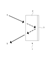
- the sheet type electromagnetic wave absorber (1) is composed of an absorber (2) lined with a metal film (3).
- the absorber (2) is made of an absorbing material.
- Part of the incident wave (4) that has entered the absorber (2) is reflected on the surface of the absorber, and the rest enters the inside of the absorber.
- the electromagnetic wave that has entered is reflected by the metal film (3), and part of it is radiated to the outside of the absorber as a reflected wave (5).
- the electromagnetic wave attenuation mechanism is classified into two types: attenuation due to interference between the incident wave (4) and the reflected wave (5) and attenuation (absorption) inside the absorber (2).
- the former (attenuation due to interference) utilizes a phenomenon in which the incident wave (4) and the reflected wave (5) cancel each other when the thickness of the absorber (2) and the wavelength of the electromagnetic wave have a specific relationship.
- the thickness of the absorber (2) needs to be strictly controlled, and the frequency of the electromagnetic wave to be attenuated is limited to a narrow band.
- the latter (attenuation inside the absorber) utilizes the loss characteristic of the absorber (2), and has an advantage that it can absorb electromagnetic waves in a wide band.
- Absorption materials that utilize loss characteristics are roughly classified into three types: conduction loss material, dielectric loss material, and magnetic loss material.
- the conductive loss material and the dielectric loss material absorb electromagnetic wave energy by electrical resistance due to movement of electrons in a substance induced by an electric field component of electromagnetic waves and polarization due to displacement of ions and/or electrons, and finally It uses the phenomenon of being converted into heat energy.
- the magnetic loss material utilizes a phenomenon in which the motion of the magnetic moment (spin) in the substance is excited by the magnetic field component of the electromagnetic wave and the electromagnetic wave energy is absorbed.
- An absorber using the loss characteristic can increase the electromagnetic wave absorption amount by making it thick.
- an excessively thick absorber is not desirable from the viewpoint of miniaturization of electronic devices. Therefore, it is desired to develop a material which has a large loss and can sufficiently absorb electromagnetic waves even if it is thin.
- Patent literature 1 discloses a dielectric sheet characterized by comprising a sheet having a thickness of 5 to 30 ⁇ m formed by drying a coating film of a coating liquid containing a resin and natural graphite powder having an average particle size of 10 ⁇ m or less. That is, the mixture of graphite powder and resin functions as a dielectric, showing a dielectric anisotropy that can obtain a particularly high dielectric constant for electromagnetic waves incident from the direction perpendicular to the sheet surface, and the direction in which the electromagnetic waves arrive on the sheet surface. It is described that the excellent electromagnetic wave absorption ability is exhibited by facing the above (Claim 1, claim [0013] and [0016]).
- Patent Document 2 mainly contains flat soft magnetic particles made of an iron-based amorphous alloy and an organic binder, and the amorphous alloy has a composition formula of ⁇ Fe a (Si x B y P z ) 1-a ⁇ 100-b L b , L is Al or the like, and an electromagnetic interference suppressor characterized by having a complex relative permeability ⁇ ′′ of 7 or more at 10 GHz is disclosed, and at 10 GHz It is described that the electromagnetic interference suppressing function due to magnetic loss can be enhanced by setting the complex relative permeability ⁇ ′′ to 7 or more (claim 1 and [0043] of Patent Document 2). Further, Non-Patent Document 1 describes that in a ferroelectric ceramic material, a dielectric loss due to relaxation of spontaneous polarization generally occurs between the MHz band and the GHz band.
- Patent Literature 3 and Non-Patent Literature 2 can be cited as literatures focusing on both dielectric loss and magnetic loss.
- Patent Document 3 describes a structure in which a high dielectric material and a high magnetic material are combined, and the high dielectric material and the high magnetic material are three-dimensionally continuous in the composite.
- an electromagnetic wave absorber characterized by having a high dielectric material and a high magnetic material continuous even in the vibration direction of the magnetic field component and electric field component of the electromagnetic wave, so that the magnetic circuit and the electric circuit are separated. It is described that it has high electromagnetic wave absorption characteristics for broadband electromagnetic waves including low frequency electromagnetic waves.
- Non-Patent Document 2 discloses that in the X band of 8.2 to 12.4 GHz, the complex dielectric of U-type hexagonal ferrite Ba 4 Mn (2-x) Zn x Fe 36 O 60 (0 ⁇ x ⁇ 2). It is described that the magnetic permeability, the magnetic permeability, and the microwave absorption characteristics are examined, and that the sample having the Ba 4 MnZnFe 36 O 60 composition can be used for suppressing the micro absorption and the electromagnetic interference.
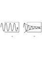
- FIG. 2A shows a case where the imaginary part of the relative permittivity and/or the relative permeability of the absorbing material is small. In this case, since the loss of the absorbing material is small, the amount of electromagnetic wave attenuation is small.
- FIG. 2B shows a case where the imaginary part of the relative permittivity and/or the relative permeability of the absorbing material is high. In this case, the loss of the absorbing material is large, the energy of the incident electromagnetic wave is quickly converted into the thermal energy of the absorbing material, and as a result, the amount of attenuation of the electromagnetic wave is large.
- the relative dielectric constant imaginary part becomes maximum at the dielectric loss peak frequency
- the relative magnetic permeability imaginary part becomes maximum at the magnetic loss peak frequency. Therefore, it is desired that the electromagnetic wave absorbing material has a loss peak frequency in a target frequency band and a high value of the imaginary part of the relative permittivity and relative permeability at that time.
- the electromagnetic wave absorbing material has the same values of relative permittivity and relative permeability. This is because if the values of relative permittivity and relative permeability are far apart, the characteristic impedance of the absorbing material will not match (match) with the impedance of air, and as a result, of the incident electromagnetic wave, it will be reflected on the absorber surface. This is because the ratio of the absorption is increased and the absorption efficiency inside the absorber is reduced.
- the values of relative permittivity and relative permeability to be approximately the same, electromagnetic wave reflection due to impedance mismatch is suppressed, and as a result, both dielectric loss and magnetic loss are effectively used for electromagnetic wave absorption. it can. For that purpose, it is desirable that the peak frequencies of the dielectric loss and the magnetic loss are close to each other.
- the electromagnetic wave absorbing material has peak frequencies of dielectric loss and magnetic loss close to each other and that the relative permittivity and the relative permeability are as high as possible.
- Patent Document 1 and Non-Patent Document 1 focus only on dielectric loss
- Patent Document 2 focus only on magnetic loss. Therefore, there is a limit to improving the electromagnetic wave absorption performance.
- Patent Document 3 discloses an electromagnetic wave absorber having a structure in which a high dielectric material and a high magnetic material are three-dimensionally continuous.
- a composite material having a three-dimensionally continuous and complicated structure has a problem that it is difficult to manufacture.
- Non-Patent Document 2 it is said that dielectric loss and magnetic loss of the same level can be obtained in the GHz band.
- the composition of the ferrite that is supposed to be realized in this document is very limited. Therefore, it is considered that in the ferrite of this document, the dielectric loss and the magnetic loss peaked only at frequencies that were accidentally close to each other.
- the present inventor shows that a composite oxide having a specific composition and crystal structure can be used as a multiferroic material, and by using this multiferroic material, the same level as in the past can be obtained. It was found that an electromagnetic wave absorber exhibiting an excellent electromagnetic wave absorption performance in a wider band can be obtained despite its thickness.
- the present invention has been completed based on such knowledge, and provides an electromagnetic wave absorbing material and an electromagnetic wave absorber that exhibit excellent electromagnetic wave absorbing performance in a wider band despite being as thick as conventional ones. Is an issue.
- the present invention includes the following aspects (1) to (10).
- the expression “to” includes numerical values at both ends thereof. That is, “X to Y” is synonymous with “X or more and Y or less”.
- the electromagnetic wave absorbing material includes a multiferroic material,
- the multiferroic material contains bismuth (Bi) and iron (Fe), and at least one selected from the group consisting of nickel (Ni), cobalt (Co), manganese (Mn) and chromium (Cr).
- Consisting of a composite oxide containing the first additive element The complex oxide is selected from the group consisting of a perovskite type structure, a double perovskite type structure, a Ruddlesden-Popper type structure, and a Dion-Jacobson type structure.
- the frequency of the electromagnetic wave absorbed by the multiferroic material is in the range of 100 MHz or more and 1 THz or less.
- the ratio (Y 1 /X Fe ) of the total molar amount (Y 1 ) of the first additive element to the molar amount (X Fe ) of iron (Fe) is more than 0.00 and 4.00 or less, The material of (1) or (2).
- the composite oxide is zinc (Zn), magnesium (Mg), calcium (Ca), strontium (Sr), barium (Ba), lead (Pb), rare earth element (RE), titanium (Ti), (1) to (3) above, further containing one or more second additive elements selected from the group consisting of niobium (Nb), zirconium (Zr), aluminum (Al), copper (Cu) and tantalum (Ta). ) Either material.
- RE rare earth element
- Ti titanium
- Nb niobium
- Zr zirconium
- Al aluminum
- Cu copper
- tantalum (Ta) tantalum
- the base material is made of one or more materials selected from the group consisting of organic substances, polymers, glass and ceramics.
- an electromagnetic wave absorbing material and an electromagnetic wave absorbing body which show excellent electromagnetic wave absorbing performance in a wider band even though they are as thick as conventional ones.
- the present embodiment A specific embodiment of the present invention (hereinafter referred to as “the present embodiment”) will be described.
- the present invention is not limited to the following embodiments, and various modifications can be made without departing from the spirit of the present invention.
- the electromagnetic wave absorbing material of the present embodiment includes a multiferroic material.
- This multiferroic material is composed of a complex oxide containing bismuth (Bi) and iron (Fe).
- the composite oxide further contains one or more first additive elements selected from the group consisting of nickel (Ni), cobalt (Co), manganese (Mn) and chromium (Cr).
- this composite oxide is composed of a perovskite structure, a double-perovskite structure, a Rudersden-Popper structure, and a Dion-Jacobson structure. It has one or more crystal structures selected.
- the frequency of electromagnetic waves absorbed by the material is in the range of 100 MHz or more and 1 THz or less.
- Multi-ferroic material is a material in which magnetic order and electric polarization order coexist.
- magnetic order means strong interaction (exchange interaction, superexchange interaction) between magnetic moments (spins) in a substance such as ferromagnetism and antiferromagnetism, and the order in the direction of magnetic moment It means a state that exists.
- the electrical polarization order is a property such as ferroelectricity or antiferroelectricity, in which electrical polarization (spontaneous polarization) occurs due to displacement of electrons and/or ions in a substance, and there is an order between those polarizations.
- multiferroic materials unlike composite materials containing dielectrics and magnetics, coexist magnetic and electrical polarization orders, such as ferromagnetism and ferroelectricity. Further, among the multiferroic materials, the material having a strong correlation between the magnetic order and the electric polarization order has a high electro-magnetic effect, and the induction of the electric polarization by the magnetic field and/or the induction of the magnetization by the electric field. It is possible.
- Multi-ferroic materials are capable of controlling the respective directions of magnetization and electric polarization, and are attracting attention for their application to multi-valued memories. Further, a multiferroic material having a high electromagnetic effect is expected to be applied to a next-generation memory capable of ON/OFF control by an electric field or a magnetic field.
- the electromagnetic wave absorbing material of the present embodiment includes a multiferroic material and is useful as an electromagnetic wave absorbing material in a wide band including the GHz band. This is because the multiferroic material having the composition specified in the present embodiment has magnetic order and electric polarization order, and has a relative permeability that contributes to magnetic loss and dielectric loss in a wide band including the GHz band. This is because the magnetic imaginary part and the relative dielectric constant imaginary part are high. Moreover, the multiferroic material has strong coupling between the magnetic order and the electric polarization order, and the magnetic loss and the dielectric loss have maximums (peaks) at frequencies close to each other.
- the multiferroic material included in the electromagnetic wave absorbing material is a composite oxide containing bismuth (Bi) and iron (Fe).
- bismuth (Bi) and iron (Fe) are the main constituent elements forming the skeleton of the crystal structure of the composite oxide. That is, the multiferroic material is composed of a bismuth (Bi)-iron (Fe)-based composite oxide.
- a multiferroic phenomenon is exhibited at room temperature by being composed of a bismuth (Bi)-iron (Fe)-based composite oxide and having a crystal structure described later.
- the complex oxide (multiferroic material) included in the electromagnetic wave absorbing material is a perovskite type structure, a double perovskite type structure, a Ruddlesden-Popper type structure, and a dion Jacobson type Dion.
- -Jacobson type structure and at least one crystal structure selected from the group consisting of
- the perovskite has a crystal structure represented by the general formula ABO 3
- the double perovskite has a crystal structure represented by the general formula A 2 BB′O 6
- Rudersden popper has a crystal structure represented by the general formula A n+1 B n O 3n+1
- Dion Jacobson has a crystal structure represented by the general formula A′A n ⁇ 1 B n O 3n+1 .
- Double perovskite, Rudersden popper and Dion Jacobson have a structure similar to perovskite, and electromagnetic wave absorption characteristics similar to those of perovskite are obtained.
- composition fluctuations are allowed as long as the desired crystal structure is obtained.
- ABO 3 of perovskite the ratio of A and B does not need to be strictly “1:1”, and deviation of the ratio is allowed as long as it shows a perovskite type crystal structure.
- there may be lattice defects such as oxygen vacancies, in which case the amount of oxygen (O) in the general formula may shift.
- the bismuth (Bi)-iron (Fe)-based composite oxide having a perovskite type crystal structure has a high ferroelectric Curie temperature and an antiferromagnetic Neel temperature (or a ferromagnetic Curie temperature), and therefore, at room temperature.
- it shows a multiferroic phenomenon.
- the bismuth (Bi)-iron (Fe)-based composite oxide having a double perovskite, Rudersden popper and Dion Jacobson type crystal structure has a multiferroic structure at room temperature because its crystal structure is similar to that of the perovskite type structure. Indicates a phenomenon.
- the composite oxide (multiferroic material) contained in the electromagnetic wave absorbing material further comprises at least one first kind selected from the group consisting of nickel (Ni), cobalt (Co), manganese (Mn) and chromium (Cr). Including additional elements.
- the inclusion of such a first additive element has the effect of increasing the macroscopic magnetization of the material. That is, the bismuth (Bi)-iron (Fe)-based composite oxide containing no first additive element has macroscopic spontaneous polarization, but has almost no macroscopic magnetization. This is because the magnetic moment (spin) due to the iron (Fe) ion is antiparallel-coupled (antiferromagnetically coupled) by the superexchange interaction via the oxygen (O) ion.
- the first additive elements (Ni, Co, Mn, and Cr) belonging to the 3d transition metal are ionized in the composite oxide and easily replace with iron (Fe) ions.
- the ionized first additive element has a different magnetic moment from the iron (Fe) ion and changes the magnetic order in the material. As a result, cancellation of magnetic moments (spins) is suppressed, and magnetization is developed as a whole.
- the ratio (Y 1 /X Fe ) of the total molar amount (Y 1 ) of the first additive element to the molar amount (X Fe ) of iron (Fe) is preferably more than 0.00 and 4.00 or less. From the viewpoint of enhancing the magnetization, it is desirable that the first additive element be contained to some extent. However, if the first additive element is excessively large, the number of different phases increases, and the electromagnetic wave absorption performance may deteriorate.
- Y 1 /X Fe is more preferably 0.01 or more, still more preferably 0.03 or more. Further, Y 1 /X Fe is more preferably 1.00 or less, still more preferably 0.50 or less.
- Y 1 /X Fe is more preferably 0.01 or more, still more preferably 0.03 or more. Further, Y 1 /X Fe is more preferably 0.50 or less, still more preferably 0.30 or less.
- the composite oxide includes zinc (Zn), magnesium (Mg), calcium (Ca), strontium (Sr), barium (Ba), lead (Pb), rare earth element (RE), titanium (Ti). ), niobium (Nb), zirconium (Zr), aluminum (Al), copper (Cu), and tantalum (Ta), and may further include one or more second additive elements selected from the group consisting of:
- the rare earth element (RE) includes scandium (Sc) and atomic number with atomic number 21.
- the second additive element replaces one or both of bismuth (Bi) and iron (Fe) in the composite oxide.
- the second additive element has a function of adjusting the balance between the dielectric loss and the magnetic loss.
- the ratio (Y 2 /X Bi ) of the amount (Y 2 ) is preferably 0.00 or more and 0.80 or less.
- Y 2 /X Bi is more preferably 0.01 or more, still more preferably 0.03 or more. Further, Y 2 /X Bi is more preferably 0.50 or less, still more preferably 0.30 or less. In particular, when the composite oxide has a perovskite structure, Y 2 /X Bi is more preferably 0.01 or more, still more preferably 0.03 or more. Further, Y 2 /X Bi is more preferably 0.50 or less, still more preferably 0.30 or less. The composite oxide may not include the second additive element.
- the frequency of electromagnetic waves absorbed by this material is in the range of 100 MHz or more and 1 THz or less.
- both the dielectric loss peak frequency ( ⁇ E ) and the magnetic loss peak frequency ( ⁇ M ) are in the range of 100 MHz or more and 1 THz or less.
- the dielectric loss peak frequency ( ⁇ E ) and the magnetic loss peak frequency ( ⁇ M ) are frequencies (dielectric resonance frequency, magnetic resonance frequency) at which the imaginary part of permittivity or the imaginary part of permeability has a maximum value (peak). That is.
- the dielectric loss peak frequency ( ⁇ E ) and the magnetic loss peak frequency ( ⁇ M ) are preferably 100 MHz or more and 100 GHz or less, and more preferably 1 GHz or more and 100 GHz or less. Furthermore, since the peak frequencies of the dielectric loss and the magnetic loss are close to each other, the electromagnetic wave absorption performance in a wide band including the GHz band can be made excellent.
- ) between the dielectric loss peak frequency ( ⁇ E ) and the magnetic loss peak frequency ( ⁇ M ) is preferably 5 GHz or less, more preferably 3 GHz or less, and 1 GHz or less. Is more preferable.
- the complex oxide preferably has a magnetic susceptibility of 1 ⁇ 10 ⁇ 2 or more.
- the magnetic susceptibility is more preferably 5 ⁇ 10 ⁇ 2 or more, further preferably 1 ⁇ 10 ⁇ 1 or more.
- the upper limit of the magnetic susceptibility is not particularly limited, it is typically 10 or less, and more typically 3 or less.
- the average particle size of the composite oxide is preferably 5 ⁇ m or less, more preferably 3 ⁇ m or less. If the particle size of the electromagnetic wave absorbing material is excessively large, the electromagnetic wave absorber containing this material may have poor surface smoothness. Further, in order to increase the particle size of the electromagnetic wave absorbing material, it is necessary to raise the firing temperature, and a component having a high vapor pressure such as bismuth (Bi) is volatilized, which may make it difficult to control the composition.
- a component having a high vapor pressure such as bismuth (Bi) is volatilized
- the compound oxide preferably has a crystallite size of 5 nm or more and 200 nm or less, more preferably 5 nm or more and 100 nm or less. If the crystallite size is excessively small, the crystallinity will be poor, and the dielectric loss and magnetic loss may decrease. On the other hand, in order to increase the crystallite size excessively, it is necessary to raise the firing temperature, which may make it difficult to control the composition.
- the electromagnetic wave absorbing material only needs to include the multiferroic material (composite oxide), and does not exclude the inclusion of other components.
- the multiferroic material composite oxide
- unavoidable impurities mixed during the production of the composite oxide are acceptable.
- a hetero phase other than the complex oxide having the above-mentioned crystal structure may be contained.
- an additive component such as a sintering aid may be contained.
- the content of the multiferroic material (composite oxide) is preferably 50% by mass or more, more preferably 70% by mass or more, and further preferably 90% by mass or more.
- the electromagnetic wave absorbing material may be composed only of the multiferroic material (composite oxide).
- the multiferroic material contains bismuth (Bi), iron (Fe), oxygen (O), a first additive element (Ni, Co, Mn, and Cr), and as long as desired electromagnetic wave absorption performance is obtained.
- the inclusion of elements other than the second additive element (Zn, Mg, Ca, Sr, Ba, Pb, RE, Ti, Nb, Zr, Al, Cu and Ta) is not excluded.
- the total content of bismuth (Bi), iron (Fe), oxygen (O), the first additional element and the second additional element is preferably 80 mol% or more, more preferably 90 mol% or more, and more preferably 95 mol% or more. More preferably, 99 mol% or more is particularly preferable.
- the shape of the electromagnetic wave absorbing material is not limited. That is, it may be in a bulk form or a powder form. Further, it may be a single crystal or a polycrystal.
- the electromagnetic wave absorbing material may be a powder, a molded body or a sintered body. Further, the electromagnetic wave absorbing material may be a thin film or a thick film.
- the electromagnetic wave absorbing material can be manufactured by a method similar to that of ordinary ceramic materials.
- a solid-state reaction method in which oxides, carbonates, oxalates, hydroxides and/or nitrates of constituent metals are mixed and further subjected to firing reaction.
- a method of producing an oxide mixture containing a constituent metal by a method such as a sol-gel method, a complex polymerization method, a freeze-drying method, a spray pyrolysis method, and firing the mixture is mentioned.
- the firing conditions are not limited as long as a material having a desired composition and crystal structure can be obtained. For example, there may be mentioned a condition of holding at a temperature of 300° C. to 1000° C. for 30 minutes to 10 hours.
- the thickness of the electromagnetic wave absorbing material of the present embodiment being about the same as the conventional one, it is possible to obtain excellent electromagnetic wave absorbing performance in a wider band.
- it can be produced by the same method as that for ordinary ceramic materials, and can be obtained easily and inexpensively.
- the electromagnetic wave absorber of the present embodiment contains the electromagnetic wave absorbing material.
- the form of the electromagnetic wave absorbing material contained is not particularly limited, and examples thereof include powder and sintered bodies.
- the electromagnetic wave absorbing material is a powder
- the electromagnetic wave absorbing material may be composed of a powder and a base material, and the powder may be dispersed in the base material.
- the base material is preferably made of one or more materials selected from the group consisting of organic substances, polymers, glass and ceramics.
- a surface treatment layer may be provided on the powder surface, and an additive other than the powder may be added to the base material.
- the usage mode of the electromagnetic wave absorber is not particularly limited and may be a known mode.
- an electromagnetic wave absorber made of a sintered body can be used as an electromagnetic wave absorbing tile of a structure.
- a bulk electromagnetic wave absorber or a sheet electromagnetic wave absorber may be used by using a powdery electromagnetic wave absorbing material dispersed in a base material.
- the bulk or sheet-shaped electromagnetic wave absorber can be used for a housing of electronic equipment, a package of electronic parts, or the like.
- the electromagnetic wave absorber may be a coating film provided on the substrate.
- Such a coating film is formed, for example, by adding a solvent and, if necessary, a binder and a dispersant to a powdery electromagnetic wave absorbing material to form a paste, and applying the obtained paste to the surface of a substrate and drying. be able to.
- a sample for evaluation was prepared from the obtained sintered body (electromagnetic wave absorber). A part of the sintered body was crushed and used as a sample for evaluation of crystal structure, spontaneous polarization and magnetic susceptibility. Further, as a sample for evaluating permittivity and magnetic permeability from 100 MHz to 20 GHz, a sintered body was processed into a toroidal shape having an outer diameter of 7 mm, an inner diameter of 1.5 mm and a thickness of 1.5 mm.
- Example 2 As raw materials, bismuth nitrate pentahydrate (Bi (NO 3) 3 ⁇ 5H 2 O), iron nitrate nonahydrate (Fe (NO 3) 3 ⁇ 9H 2 O) and cobalt nitrate hexahydrate (Co ( NO 3) 2 ⁇ 6H 2 O ) used, except that the composition of the resulting product was weighed so as to have the composition shown in Table 1, in the same manner as in example 1, subjected to fabrication of the electromagnetic wave absorbing material It was Regarding the evaluation, in addition to the same evaluation as in Example 1, the evaluation of the dielectric constant and the magnetic permeability from 20 GHz to 110 GHz was performed.
- Bi (NO 3) 3 ⁇ 5H 2 O bismuth nitrate pentahydrate
- Fe (NO 3) 3 ⁇ 9H 2 O iron nitrate nonahydrate
- Co ( NO 3) 2 ⁇ 6H 2 O cobalt nitrate hexahydrate
- the sintered body was processed into a plate shape of 120 mm ⁇ 120 mm ⁇ 1 mm to obtain a sample for permittivity and magnetic permeability evaluation from 20 GHz to 110 GHz.
- This sample was prepared by newly producing 150 g of a sintered body using the same method as in Example 1.
- Example 3 As raw materials, bismuth nitrate pentahydrate (Bi (NO 3) 3 ⁇ 5H 2 O), iron nitrate nonahydrate (Fe (NO 3) 3 ⁇ 9H 2 O) and cobalt nitrate hexahydrate (Co ( NO 3) 2 ⁇ 6H 2 O ) used, except that the resulting product was weighed so as to have the composition shown in Table 1, in the same manner as in example 1 were prepared and evaluation of the electromagnetic wave absorbing material ..
- Bi (NO 3) 3 ⁇ 5H 2 O bismuth nitrate pentahydrate
- Fe (NO 3) 3 ⁇ 9H 2 O iron nitrate nonahydrate
- Co ( NO 3) 2 ⁇ 6H 2 O cobalt nitrate hexahydrate
- Example 4 As raw materials, bismuth nitrate pentahydrate (Bi (NO 3) 3 ⁇ 5H 2 O), iron nitrate nonahydrate (Fe (NO 3) 3 ⁇ 9H 2 O), manganese nitrate hexahydrate (Mn ( NO 3) using a 2 ⁇ 6H 2 O) and nickel nitrate hexahydrate (Ni (NO 3) 2 ⁇ 6H 2 O), except that the resulting product was weighed so as to have the composition shown in Table 1 In the same manner as in Example 1, an electromagnetic wave absorbing material was prepared and evaluated.
- Example 5 As raw materials, bismuth nitrate pentahydrate (Bi (NO 3) 3 ⁇ 5H 2 O), iron nitrate nonahydrate (Fe (NO 3) 3 ⁇ 9H 2 O), neodymium nitrate hexahydrate (Nd ( NO 3) 3 ⁇ 6H 2 O ), except that using a cobalt nitrate hexahydrate (Co (NO 3) 2 ⁇ 6H 2 O), the resulting product was weighed so as to have the composition shown in Table 1 In the same manner as in Example 1, an electromagnetic wave absorbing material was prepared and evaluated.
- Example 6 As raw materials, bismuth nitrate pentahydrate (Bi (NO 3) 3 ⁇ 5H 2 O), iron nitrate nonahydrate (Fe (NO 3) 3 ⁇ 9H 2 O), calcium nitrate tetrahydrate (Ca ( NO 3) 2 ⁇ 4H 2 O ), except that using a cobalt nitrate hexahydrate (Co (NO 3) 2 ⁇ 6H 2 O), the resulting product was weighed so as to have the composition shown in Table 1 In the same manner as in Example 1, an electromagnetic wave absorbing material was prepared and evaluated.
- Example 7 As raw materials, bismuth nitrate pentahydrate (Bi (NO 3) 3 ⁇ 5H 2 O), iron nitrate nonahydrate (Fe (NO 3) 3 ⁇ 9H 2 O), neodymium nitrate hexahydrate (Nd ( NO 3) using the 3 ⁇ 6H 2 O) and cobalt nitrate hexahydrate (Co (NO 3) 2 ⁇ 6H 2 O), except that the resulting product was weighed so as to have the composition shown in Table 1 In the same manner as in Example 1, an electromagnetic wave absorbing material was prepared and evaluated.
- Example 8 As raw materials, bismuth nitrate pentahydrate (Bi (NO 3) 3 ⁇ 5H 2 O), iron nitrate nonahydrate (Fe (NO 3) 3 ⁇ 9H 2 O) and cobalt nitrate hexahydrate (Co ( NO 3) 2 ⁇ 6H 2 O ) using the composition of the product obtained was weighed so as to have the composition shown in Table 1. The same procedure as in Examples 1 to 7 was performed until the precursor solution and the precursor powder were obtained. Then, press molding was performed and firing was performed under the condition of holding at 600° C. for 2 hours, and evaluation was performed in the same manner as in Examples 1 to 7. That is, Example 8 is an example in which the firing conditions were changed with the same composition as in Example 2.
- Example 9 As raw materials, bismuth nitrate pentahydrate (Bi (NO 3) 3 ⁇ 5H 2 O), iron nitrate nonahydrate (Fe (NO 3) 3 ⁇ 9H 2 O), neodymium nitrate hexahydrate (Nd ( NO 3) using the 3 ⁇ 6H 2 O) and cobalt nitrate hexahydrate (Co (NO 3) 2 ⁇ 6H 2 O), except that the resulting product was weighed so as to have the composition shown in Table 1 Was prepared and evaluated under the same conditions as in Example 8. That is, Example 9 is an example in which the firing conditions were changed with the same composition as in Example 7.
- Example 10 (comparative example) Bismuth nitrate pentahydrate (Bi(NO 3 ) 3 .5H 2 O) and iron nitrate nonahydrate (Fe(NO 3 ) 3 .9H 2 O) were used as raw materials, and the obtained products are shown in Table 1.
- An electromagnetic wave absorbing material was prepared and evaluated in the same manner as in Example 1 except that the composition was weighed so that the composition shown in FIG.
- Example 11 (comparative example) As a raw material, using a bismuth nitrate pentahydrate (Bi (NO 3) 3 ⁇ 5H 2 O) and ferric nitrate nonahydrate (Fe (NO 3) 3 ⁇ 9H 2 O), the resulting product Table 1 An electromagnetic wave absorbing material was prepared and evaluated in the same manner as in Example 8 except that the composition was weighed so that the composition shown in FIG. That is, Example 11 is an example in which the firing conditions were changed with the same composition as Example 10.
- Example 12 (comparative example) As raw materials, bismuth nitrate pentahydrate (Bi (NO 3) 3 ⁇ 5H 2 O), iron nitrate nonahydrate (Fe (NO 3) 3 ⁇ 9H 2 O) and neodymium nitrate hexahydrate (Nd ( NO 3) 3 ⁇ 6H 2 O ) used, except that the resulting product was weighed so as to have the composition shown in Table 1, in the same manner as in example 1 were prepared and evaluation of the electromagnetic wave absorbing material ..
- Example 13 (comparative example) As raw materials, bismuth nitrate pentahydrate (Bi (NO 3) 3 ⁇ 5H 2 O), iron nitrate nonahydrate ( With Fe (NO 3) 3 ⁇ 9H 2 O) and cobalt nitrate hexahydrate (Co (NO 3) 2 ⁇ 6H 2 O), the resulting product subjected weighed so as to have the composition shown in Table 1 An electromagnetic wave absorbing material was prepared and evaluated in the same manner as in Example 1 except for the above.
- Example 14 (comparative example) As raw materials, bismuth nitrate pentahydrate (Bi (NO 3) 3 ⁇ 5H 2 O), iron nitrate nonahydrate (Fe (NO 3) 3 ⁇ 9H 2 O), neodymium nitrate hexahydrate (Nd ( NO 3) using the 3 ⁇ 6H 2 O) and cobalt nitrate hexahydrate (Co (NO 3) 2 ⁇ 6H 2 O), except that the resulting product was weighed so as to have the composition shown in Table 1 In the same manner as in Example 1, an electromagnetic wave absorbing material was prepared and evaluated.
- Example 15 As a raw material of strontium nitrate tetrahydrate (Sr (NO 3) 2 ⁇ 4H 2 O), iron nitrate nonahydrate (Fe (NO 3) 3 ⁇ 9H 2 O), cobalt nitrate hexahydrate (Co ( NO 3) using a 2 ⁇ 6H 2 O) and titanium tetrabutoxide (Ti (OC 4 H 9) 4), the product obtained is subjected weighed so as to have the composition shown in Table 1, 5 fired at 1200 ° C. An electromagnetic wave absorber was prepared and evaluated in the same manner as in Example 1 except that the conditions were such that it was held for a time. Since the composition of Example 12 was significantly different from that of Examples 1 to 14, the firing conditions were changed. The composition of this product is that of magnetoplumbite type hexagonal ferrite having ferromagnetism but no ferroelectricity.
- ⁇ ′ and ⁇ ′′ are the real part and the imaginary part of the complex relative permittivity, respectively
- ⁇ ′ and ⁇ ′′ are the real part and the imaginary part of the complex relative permeability, respectively.
- j is an imaginary unit.
- each of the dielectric loss peak frequency ( ⁇ E ) and the magnetic loss peak frequency ( ⁇ M ) was obtained from the frequency at which each imaginary part of the permittivity and the magnetic permeability has the maximum value in the above measurement frequency range.
- ) was determined.
- the results obtained are shown in Table 1.
- the reflection and transmission characteristics from 20 GHz to 110 GHz were measured by the free space method, and the dielectric constant and magnetic permeability in the same frequency band were calculated from the reflection and transmission characteristics.
- Example 10 is BiFeO 3 , which is a well-known multiferroic material. As shown in Table 1, it was confirmed to have a perovskite structure, and spontaneous polarization was also confirmed. However, the value of magnetic susceptibility was as small as 5 ⁇ 10 ⁇ 4 . This is considered to be because in BiFeO 3 , the magnetization of iron ions (Fe 3+ ) that are magnetic ions has a very small response to a magnetic field due to antiferromagnetic coupling between different sites. As can be seen from Table 1, Example 10 has a high imaginary part of relative permittivity ( ⁇ ′′), and a dielectric loss can be expected.
- ⁇ ′′ imaginary part of relative permittivity
- Example 10 the value of the imaginary part ( ⁇ ′′) of the relative magnetic permeability is very small, and sufficient magnetic loss is not obtained. This is presumed to be because BiFeO 3 has almost no magnetization that responds to the magnetic field, as indicated by the magnetic susceptibility. As a result, in Example 10, it is considered that magnetic loss hardly occurs, like the conventional absorber that utilizes only dielectric loss. Also, although the peak of the imaginary part of relative permittivity ( ⁇ ′′) was confirmed, the clear peak of the imaginary part of relative permeability ( ⁇ ′′) could not be confirmed, and the difference in peak frequency (
- Example 1 is an example in which a cobalt (Co) element is added.
- the perovskite structure and spontaneous polarization can be confirmed, and the magnetic susceptibility is increased to about 40 times. It is considered that this is because the addition of cobalt (Co) weakened the cancellation of the magnetization generated in BiFeO 3 and exhibited weak ferromagnetism.
- the value of the relative magnetic permeability imaginary part ( ⁇ ′′) is greatly increased while the dielectric loss of the same degree as in Example 10 is obtained. This is considered to be due to an increase in magnetic susceptibility.
- Example 1 is an electromagnetic wave absorber that utilizes both loss because both dielectric loss and magnetic loss occur at frequencies close to each other. Moreover, since the values of the relative permittivity imaginary part ( ⁇ ′′) and the relative permeability imaginary part ( ⁇ ′′) are close to each other, impedance matching is easy to realize, which is advantageous for realizing an electromagnetic wave absorbing material having high absorption ability. .. In addition, the imaginary part of the relative permittivity ( ⁇ ′′) and the imaginary part of the relative permeability ( ⁇ ′′) both show broad peaks, and take a finite value in the entire measurement range of 100 MHz to 20 GHz.
- Example 1 and Example 10 had a value of about 60 to 70 nm, and it is considered that the effect of the additive element is small.
- SEM scanning electron microscope
- Examples 2 and 3 are examples in which a part of iron (Fe) of BiFeO 3 was replaced with cobalt (Co), and the replacement amount was increased as compared with Example 1.
- Fe iron
- Co cobalt
- the same perovskite structure as in Example 1 was present and a different phase was present. Further, the amount of the different phase was larger in Example 3 in which the amount of Co added was increased.
- the synthesis method used this time suggests that there is a limit to the amount of cobalt (Co) that can be solid-dissolved in BiFeO 3 .
- the ratio of the perovskite structure is high, it retains ferroelectricity and ferromagnetism.
- Example 2 the dielectric constant and magnetic permeability were also measured in the frequency range of 20 GHz to 110 GHz. As a result, it was found that the values of both imaginary parts are finite values up to about 80 to 90 GHz. This indicates that the multiferroic material of this embodiment has a capability of causing a loss with respect to electromagnetic waves of a wide frequency including the GHz band. As a cause of this, it is generally known that a ferroelectric ceramic material causes a dielectric loss due to relaxation of spontaneous polarization between the MHz band and the GHz band. In a multiferroic material, this loss causes a magnetic loss. It is thought that it also spread.
- Example 4 is an example in which part of iron (Fe) is replaced with nickel (Ni) and manganese (Mn), but the structure and properties similar to Example 2 are obtained. It was also confirmed that the same effect can be obtained by replacing with chromium (Cr).
- Example 5 and Example 6 are examples in which a part of bismuth (Bi) in Example 1 was replaced with neodymium (Nd) or calcium (Ca), respectively.
- neodymium (Nd) or calcium (Ca) As in Example 1, a perovskite structure and finite spontaneous polarization could be confirmed, and a magnetic susceptibility similar to that in Example 1 could be confirmed.
- the maximum values of both the imaginary part of relative permittivity ( ⁇ ′′) and the imaginary part of relative permeability ( ⁇ ′′) were slightly increased.
- the second additive elements other than neodymium (Nd) and calcium (Ca) if the amount of substitution is small, the multiferroic property is not lost and the dielectric and magnetic properties are slightly changed, so that the electromagnetic wave absorption performance can be adjusted. confirmed.
- Example 7 is an example in which a part of bismuth (Bi) in Example 2 is replaced with neodymium (Nd). However, the substitution amount of bismuth (Bi) is increased as compared with Examples 5 and 6.
- Example 7 as in Example 2, a part of the different phases was generated together with the perovskite structure, and the ratio of the different phases was increased. Further, as compared with Example 2, the maximum value of the relative permittivity imaginary part ( ⁇ ′′) is decreased and the maximum value of the relative magnetic permeability imaginary part ( ⁇ ′′) is increased. The decrease in the imaginary part of the relative permittivity ( ⁇ ′′) did not occur in Examples 5 and 6, suggesting a relationship with a different phase.
- Example 8 has the same composition as that of Example 2, and was prepared under the same conditions as Example 2 up to the precursor powder. However, when producing the sintered body, firing was performed under the condition of holding at 600° C. for 2 hours. By lowering the firing temperature, a decrease in crystallite size was confirmed as compared with Example 2. Further, although a different phase appeared as in Example 2, the ratio of the different phase decreased. As a cause of this, it is conceivable that part of the perovskite structure is decomposed into another structure under the firing condition of 950°C. Focusing on the dielectric and magnetic properties, although the imaginary part of relative permittivity ( ⁇ ′′) did not change so much as in Example 2, a significant increase was observed in the imaginary part of relative permeability ( ⁇ ′′). .. This is considered to be due to the reduction of out-of-phase.
- Example 9 has the same composition as that of Example 7, but was fired under the conditions of holding at 600° C. for 2 hours as in Example 8. It was confirmed that the ratio of different phases was lower than that of Example 7 and that the imaginary part ( ⁇ ′′) of relative permeability was increased. As the cause of this, as in the case of Example 8, the decomposition of the perovskite structure was suppressed by lowering the firing temperature.
- Example 2 As in Example 1, the relative permittivity imaginary part ( ⁇ ′′) and the relative permeability imaginary part ( ⁇ ′′) have finite values in the entire range of 100 MHz to 20 GHz, and dielectric loss and It was an electromagnetic wave absorber that utilized both magnetic loss.
- Example 11 As in Examples 8 and 9, firing was performed under the condition of holding at 600° C. for 2 hours. However, the composition was BiFeO 3 , which was the same as in Example 10, and no addition of Cr, Mn, Co, or Ni was performed. As compared with Example 10, almost no change was observed in the imaginary part of relative permittivity ( ⁇ ′′) and the imaginary part of relative permeability ( ⁇ ′′).
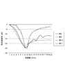
- FIG. 3 shows the results of comparing the absorption characteristics (return loss (RL)) at 1 GHz to 20 GHz for Example 2, Example 8, Example 10, and Example 11.
- f is frequency
- d sample thickness
- c speed of light.
- Example 10 and 11 which have a dielectric loss but a small magnetic loss
- the bands in which absorption of 90% (-10 dB) or more occurs are 7 to 10 GHz and 3 GHz.
- Examples 2 and 8 in which dielectric loss and magnetic loss occur close to each other, absorption of 90% or more occurs in the band of 5 GHz to over 20 GHz. From this, it was confirmed that an absorber functioning in a wider band was realized.
- Example 8 it was confirmed that the absorption amount increased particularly above 10 GHz as compared with Example 2. It is considered that this is due to the improvement of the magnetic permeability imaginary part ( ⁇ ′′).
- Example 12 as compared with Example 7, the amount of bismuth (Bi) replaced with neodymium (Nd) was about the same, but iron (Fe) was not replaced with cobalt (Co). It can be seen that the magnetic susceptibility and the relative magnetic permeability imaginary part ( ⁇ ′′) are significantly reduced, and the performance as the electromagnetic wave absorber is reduced as compared with Example 7.
- Example 13 is an excessive amount of cobalt (Co) with respect to the amount of iron (Fe), and Example 14 is an excessive amount of neodymium (Nd) with respect to the amount of bismuth (Bi).
- Co cobalt
- Nd neodymium
- Bi bismuth
- Example 15 is the same measurement performed on a magnetoplumbite ferrite showing ferromagnetism, which is not a multiferroic material. A dielectric loss peak and a magnetic loss peak were observed, but the peak frequencies were different. This is probably because, unlike the multiferroic material, there is no coupling between electric polarization order and magnetic order.
Landscapes
- Chemical & Material Sciences (AREA)
- Engineering & Computer Science (AREA)
- Power Engineering (AREA)
- Materials Engineering (AREA)
- Ceramic Engineering (AREA)
- Dispersion Chemistry (AREA)
- Organic Chemistry (AREA)
- Metallurgy (AREA)
- Crystallography & Structural Chemistry (AREA)
- Inorganic Chemistry (AREA)
- Manufacturing & Machinery (AREA)
- Microelectronics & Electronic Packaging (AREA)
- Structural Engineering (AREA)
- Shielding Devices Or Components To Electric Or Magnetic Fields (AREA)
- Inorganic Compounds Of Heavy Metals (AREA)
- Hard Magnetic Materials (AREA)
- Soft Magnetic Materials (AREA)
Abstract
従来と同定の肉厚で、より広帯域な電磁波吸収体を得られる電磁波吸収材料及び該材料を含む電磁波吸収体が提供される。電磁波吸収材料であって、前記電磁波吸収材料がマルチフェロイック材料を含み、前記マルチフェロイック材料が、ビスマス(Bi)及び鉄(Fe)を含み、さらにニッケル(Ni)、コバルト(Co)、マンガン(Mn)及びクロム(Cr)からなる群から選択される1種以上の第1添加元素を含む複合酸化物からなり、前記複合酸化物が、ペロブスカイト(Perovskite)型構造、ダブルペロブスカイト(Double-Perovskite)型構造、ルデルスデンポッパー(Ruddlesden-Popper)型構造及びディオンジャコブソン(Dion-Jacobson)型構造からなる群から選択される1種以上の結晶構造を有し、前記マルチフェロイック材料が吸収する電磁波の周波数は、100MHz以上1THz以下の範囲内にある、材料。
Description
本発明は、電磁波吸収材料及び電磁波吸収体に関する。
情報通信の高速度化や車載用レーダー等の用途でGHz帯の電波通信の発展が、今後予想されている。一方で、電子機器の増大による外部からのノイズ、デバイスの集積化に伴って深刻化している機器内のノイズの干渉対策(EMC対策)が必須である。しかしながら、このようなEMC対策を回路設計単体で行うことは困難な場合が多い。この問題を解決する一手段として、磁性材料又は誘電材料の焼結体、あるいは磁性材、誘電材又は導電材等の複合材料からなる電磁波(電波)吸収材料、及びそれを利用した電磁波吸収体(ノイズ抑制シート)が用いられている。
シート型電磁波吸収体の基本的構成を、断面模式図を用いて、図1に示す。シート型電磁波吸収体(1)は、金属膜(3)で裏打ちされた吸収体(2)で構成されている。吸収体(2)は吸収材料で構成されている。吸収体(2)に入射した入射波(4)は、一部が吸収体表面で反射され、残りは吸収体内部に侵入する。侵入した電磁波は金属膜(3)で反射され、その一部が反射波(5)として吸収体外部へ放射される。電磁波減衰メカニズムは、入射波(4)と反射波(5)の干渉による減衰と吸収体(2)の内部での減衰(吸収)の2つに分類される。前者(干渉による減衰)は、吸収体(2)の厚さと電磁波の波長が特定の関係にあるとき、入射波(4)と反射波(5)が打ち消しあうという現象を利用するものである。しかしながら、吸収体(2)の厚さを厳密に制御する必要があるとともに、減衰される電磁波の周波数が狭帯域に限定される。一方で、後者(吸収体内部での減衰)は、吸収体(2)の損失特性を利用するものであり、広帯域の電磁波を吸収できる利点がある。
損失特性を利用した吸収材料は、導電損失材料、誘電損失材料及び磁気損失材料の3種に大別される。このうち、導電損失材料や誘電損失材料は、電磁波の電界成分によって誘起される物質中の電子の移動による電気抵抗や、イオン及び/又は電子の変位による分極によって、電磁波エネルギーが吸収され、最終的に熱エネルギーに変換される現象を利用している。一方で、磁気損失材料は、電磁波の磁界成分によって物質中の磁気モーメント(スピン)の運動が励起され、電磁波エネルギーが吸収される現象を利用している。損失特性を利用した吸収体は、これを厚くすることで、電磁波吸収量を高めることが可能である。しかしながら、過度に厚い吸収体は、電子機器の小型化の観点から望ましくない。そのため、損失量が大きく、薄肉でも電磁波吸収を十分に行える材料の開発が望まれている。
誘電損失及び磁気損失の一方に着目した文献として、特許文献1、特許文献2及び非特許文献1が挙げられる。特許文献1には、樹脂及び平均粒径10μm以下の天然黒鉛粉末を含む塗工液の塗膜を乾燥して形成された厚み5~30μmのシートからなることを特徴とする誘電体シートが開示され、黒鉛粉末と樹脂の混合物は誘電体として機能する旨、シート表面に対する垂直方向から入射する電磁波に対して特に高い誘電率が得られる誘電異方性を示し、シート表面を電磁波が到来する方向に対面させることで、優れた電磁波吸収能力を発揮する旨が記載されている(特許文献1の請求項1、[0013]及び[0016])。
また、特許文献2には、鉄系非晶質合金からなる扁平状の軟磁性粒子と、有機結合剤を主に含有し、前記非晶質合金は、組成式が{Fea(SixByPz)1-a}100-bLb、LはAl等であり、10GHzにおける複素比透磁率μ’’が7以上であることを特徴とする電磁干渉抑制体が開示され、10GHzにおける複素比透磁率のμ’’を7以上とすることで、磁気損失による電磁干渉抑制機能を高めることができる旨が記載されている(特許文献2の請求項1及び[0043])。さらに、非特許文献1には、一般に、強誘電体セラミック材料において、MHz帯からGHz帯の間に、自発分極の緩和に起因する誘電損失が生じる旨が記載されている。
一方で、誘電損失と磁気損失の双方に着目した文献として、特許文献3及び非特許文献2が挙げられる。特許文献3には、高誘電性材料と高磁性材料とが複合された複合体からなり、前記複合体中において前記高誘電性材料と前記高磁性材料とがそれぞれ三次元的に連続した構造を有することを特徴とする電磁波吸収体が開示され、電磁波の磁界成分及び電界成分の振動方向に対しても高誘電性材料及び高磁性材料が連続しているので、磁気回路及電気回路が分断されることなく、低周波の電磁波を含む広帯域の電磁波に対して高い電磁波吸収特性を備える旨が記載されている。また、非特許文献2には、8.2~12.4GHzのXバンドにおいて、U型六方晶フェライトBa4Mn(2-x)ZnxFe36O60(0≦x≦2)の複素誘電率、透磁率及びマイクロ波吸収特性を調べる旨、Ba4MnZnFe36O60組成を有するサンプルが、マイクロ吸収及び電気磁気干渉の抑制に利用できる旨が記載されている。
T.Teranishi, Broadband spectroscopy of dielectrics and oxygen-ion conductors, Journal of the Ceramic Society of Japan, 157 [7] (2017), 547-551
R.S.Meena et al., Complex permittivity, permeability and microwave absorbing properties of (Mn2-xZnx)U-type hexaferrite, Journal of Magnetism and Magnetic Materials, 322 (2010), 2908-2914
電子機器等のさらなる高周波化、広帯域化及び小型化の要求に応じて、薄肉で且つ広帯域で電磁波吸収性能(損失特性)が優れた電磁波吸収材料が求められている。そして、この要求に答えるには、電磁波吸収材料の誘電損失及び/又は磁気損失が大きいほど望ましい。
誘電損失及び磁気損失の指標として、比誘電率の虚部と比透磁率の虚部の値が性能指数の一つとして用いられており、これらの値が高いほど損失が大きく、電磁波が早く減衰する。このことを、図2(a)及び(b)を用いて説明する。図2(a)は、吸収材料の比誘電率及び/又は比透磁率の虚部が小さい場合である。この場合には、吸収材料の損失が小さいため、電磁波の減衰量は小さい。一方、図2(b)は、吸収材料の比誘電率及び/又は比透磁率の虚部が高い場合である。この場合には、吸収材料の損失が大きく、入射電磁波のエネルギーが速やかに吸収材料の熱エネルギーに変換され、その結果、電磁波の減衰量が大きい。
また、比誘電率虚部(誘電損失)は誘電損失ピーク周波数で最大となり、比透磁率虚部(磁気損失)は磁気損失ピーク周波数で最大となる。したがって、電磁波吸収材料は、その損失ピーク周波数が目的の周波数帯域にあるとともに、そのときの比誘電率及び比透磁率の虚部の値が高いことが望まれる。
これに加えて、電磁波吸収材料は、その比誘電率と比透磁率の値が同程度であることが望まれる。これは、比誘電率と比透磁率の値が極端に離れていると、吸収材料の特性インピーダンスが空気のインピーダンスと整合(マッチング)しなくなり、その結果、入射電磁波のうち、吸収体表面で反射される割合が多くなり、吸収体内部での吸収効率が低下してしまうからである。これに対して、比誘電率と比透磁率の値を同程度にすることで、インピーダンス不整合による電磁波反射が抑えられ、その結果、誘電損失及び磁気損失の双方を電磁波吸収に効果的に利用できる。そのためには、誘電損失と磁気損失のピーク周波数が近接していることが望ましい。
このように、電磁波吸収材料は、その誘電損失と磁気損失のピーク周波数が近接し且つ比誘電率と比透磁率の値が同程度に高いことが望まれる。
しかしながら、従来の材料では、この要求に答えるには限界があった。大半の材料では、誘電損失と磁気損失の間の相関が小さく、そのため、誘電損失と磁気損失のピーク周波数を近接させ且つ比誘電率と比透磁率の値を同程度とするのは困難であったからである。
例えば、特許文献1及び非特許文献1では誘電損失のみに着目し、特許文献2では磁気損失のみに着目している。そのため、電磁波吸収性能の向上には限界がある。特許文献3では、高誘電性材料と高磁性材料が三次元的に連続した構造を有する電磁波吸収体が開示されている。しかしながら、高誘電性材料と高磁性材料の特性を整合させる必要があり、材料選択の自由度が低いという問題がある。その上、三次元的に連続した複雑な構造を有する複合材料は、製造が困難という問題がある。非特許文献2では、GHz帯域において、同程度の誘電損失及び磁気損失が得られるとされている。しかしながら、この文献で実現されるとされるフェライトは、その組成が非常に限られている。このため、この文献のフェライトでは、偶発的に近接した周波数で誘電損失及び磁気損失がピークとなったにすぎないと考えられる。
本発明者は、今般、詳細な検討を行った結果、特定の組成及び結晶構造を有する複合酸化物がマルチフェロイック材料となり得ること、及びこのマルチフェロイック材料を用いることで、従来と同程度の肉厚であるにもかかわらず、より広帯域で優れた電磁波吸収性能を示す電磁波吸収体が得られるとの知見を得た。
本発明は、このような知見に基づき完成されたものであり、従来と同程度の肉厚であるにもかかわらず、より広帯域で優れた電磁波吸収性能を示す電磁波吸収材料及び電磁波吸収体の提供を課題とする。
本発明は、下記(1)~(10)の態様を包含する。なお、本明細書において、「~」なる表現は、その両端の数値を含む。すなわち、「X~Y」は「X以上Y以下」と同義である。
(1)電磁波吸収材料であって、
前記電磁波吸収材料がマルチフェロイック材料を含み、
前記マルチフェロイック材料が、ビスマス(Bi)及び鉄(Fe)を含み、さらにニッケル(Ni)、コバルト(Co)、マンガン(Mn)及びクロム(Cr)からなる群から選択される1種以上の第1添加元素を含む複合酸化物からなり、
前記複合酸化物が、ペロブスカイト(Perovskite)型構造、ダブルペロブスカイト(Double-Perovskite)型構造、ルデルスデンポッパー(Ruddlesden-Popper)型構造及びディオンジャコブソン(Dion-Jacobson)型構造からなる群から選択される1種以上の結晶構造を有し、
前記マルチフェロイック材料が吸収する電磁波の周波数は、100MHz以上1THz以下の範囲内にある、材料。
(2)前記マルチフェロイック材料は、誘電損失ピーク周波数(ωE)及び磁気損失ピーク周波数(ωM)の両方が100MHz以上1THz以下の範囲内にある、上記(1)の材料。
(3)鉄(Fe)のモル量(XFe)に対する第1添加元素の合計モル量(Y1)の比(Y1/XFe)が、0.00超4.00以下である、上記(1)又は(2)の材料。
(4)前記複合酸化物が、亜鉛(Zn)、マグネシウム(Mg)、カルシウム(Ca)、ストロンチウム(Sr)、バリウム(Ba)、鉛(Pb)、希土類元素(RE)、チタン(Ti)、ニオブ(Nb)、ジルコニウム(Zr)、アルミニウム(Al)、銅(Cu)及びタンタル(Ta)からなる群から選択される1種以上の第2添加元素をさらに含む、上記(1)~(3)のいずれかの材料。
(5)前記複合酸化物中のビスマス(Bi)のモル量(XBi)に対する亜鉛(Zn)、マグネシウム(Mg)、カルシウム(Ca)、ストロンチウム(Sr)、バリウム(Ba)、鉛(Pb)、希土類元素(RE)、チタン(Ti)、ニオブ(Nb)、ジルコニウム(Zr)、アルミニウム(Al)、銅(Cu)及びタンタル(Ta)からなる群から選択される1種以上の第2添加元素の合計モル量(Y2)の比(Y2/XBi)が、0.00以上0.80以下である、上記(1)~(4)のいずれかの材料。
(6)前記電磁波吸収材料が、粉末、成形体又は焼結体である、上記(1)~(5)のいずれかの材料。
(7)上記(1)~(6)のいずれかの材料を含有する、電磁波吸収体。
(8)前記電磁波吸収材料が粉末であり、該粉末と母材とからなり、該粉末が母材中に分散されてなる、上記(7)の電磁波吸収体。
(9)前記母材が、有機物、高分子、ガラス及びセラミックスからなる群から選択される1種以上の材料からなる、上記(8)の電磁波吸収体。
(10)前記電磁波吸収材料が焼結体である、上記(7)の電磁波吸収体。
本発明によれば、従来と同程度の肉厚であるにもかかわらず、より広帯域で優れた電磁波吸収性能を示す電磁波吸収材料及び電磁波吸収体が提供される。
本発明の具体的な実施形態(以下、「本実施形態」という)について説明する。なお本発明は以下の実施形態に限定されるものではなく、本発明の要旨を変更しない範囲において種々の変更が可能である。
電磁波吸収材料
本実施形態の電磁波吸収材料は、マルチフェロイック材料を含む。このマルチフェロイック材料は、ビスマス(Bi)及び鉄(Fe)を含む複合酸化物からなる。この複合酸化物は、さらにニッケル(Ni)、コバルト(Co)、マンガン(Mn)及びクロム(Cr)からなる群から選択される1種以上の第1添加元素を含む。また、この複合酸化物は、ペロブスカイト(Perovskite)型構造、ダブルペロブスカイト(Double-Perovskite)型構造、ルデルスデンポッパー(Ruddlesden-Popper)型構造及びディオンジャコブソン(Dion-Jacobson)型構造からなる群から選択される1種以上の結晶構造を有する。さらに、このマルチフェロイック材料は、材料が吸収する電磁波の周波数が100MHz以上1THz以下の範囲内にある。
本実施形態の電磁波吸収材料は、マルチフェロイック材料を含む。このマルチフェロイック材料は、ビスマス(Bi)及び鉄(Fe)を含む複合酸化物からなる。この複合酸化物は、さらにニッケル(Ni)、コバルト(Co)、マンガン(Mn)及びクロム(Cr)からなる群から選択される1種以上の第1添加元素を含む。また、この複合酸化物は、ペロブスカイト(Perovskite)型構造、ダブルペロブスカイト(Double-Perovskite)型構造、ルデルスデンポッパー(Ruddlesden-Popper)型構造及びディオンジャコブソン(Dion-Jacobson)型構造からなる群から選択される1種以上の結晶構造を有する。さらに、このマルチフェロイック材料は、材料が吸収する電磁波の周波数が100MHz以上1THz以下の範囲内にある。
マルチフェロイック材料とは、磁気秩序及び電気分極秩序が共存する材料のことである。ここで、磁気秩序とは、強磁性や反強磁性など、物質中の磁気モーメント(スピン)間に強い相互作用(交換相互作用、超交換相互作用)があり、磁気モーメントの方向に秩序性が存在する状態を意味する。また、電気分極秩序とは、強誘電性や反強誘電性など、物質中の電子及び/又はイオンの変位に基づく電気分極(自発分極)が生じ、それらの分極の間に秩序性がある性質を意味する。マルチフェロイック材料は、誘電体及び磁性体を含む複合材料とは異なり、単一物質であるにもかかわらず、磁気秩序及び電気分極秩序、例えば、強磁性及び強誘電性が共存する。また、マルチフェロイック材料のうち、磁気秩序及び電気分極秩序の間に強い相関がある材料は、高い電気磁気効果を有しており、磁場による電気分極の誘起及び/又は電場による磁化の誘起が可能である。
マルチフェロイック材料は、磁化及び電気分極のそれぞれの向きを制御することが可能であり、多値メモリへの適用を目指して注目されている。また、高い電気磁気効果を有するマルチフェロイック材料は、電場や磁場によるON-OFF制御可能な次世代メモリへの適用が期待されている。
本実施形態の電磁波吸収材料は、マルチフェロイック材料を含み、GHz帯域を含む広帯域における電磁波吸収材料として有用である。これは、本実施形態で特定される組成を有するマルチフェロイック材料は、磁気秩序及び電気分極秩序を有しており、GHz帯域を含む広帯域で、磁気損失及び誘電損失のそれぞれに寄与する比透磁率虚部及び比誘電率虚部が高いためである。その上、このマルチフェロイック材料は、磁気秩序及び電気分極秩序の間に強い結合があり、磁気損失及び誘電損失が近接した周波数で極大(ピーク)となる。そのため、インピーダンス不整合による電磁波反射が抑えられるとともに、誘電損失及び磁気損失の双方を効果的に電磁波吸収に利用でき、その結果、従来と同程度の肉厚であるにもかかわらず、より広帯域で優れた電磁波吸収性能が得られる。
電磁波吸収材料に含まれるマルチフェロイック材料は、ビスマス(Bi)及び鉄(Fe)を含む複合酸化物からなる。ここで、ビスマス(Bi)及び鉄(Fe)は複合酸化物の結晶構造の骨格を形成する主要構成元素となるものである。すなわち、マルチフェロイック材料は、ビスマス(Bi)-鉄(Fe)系複合酸化物からなる。ビスマス(Bi)-鉄(Fe)系複合酸化物で構成し且つ後述する結晶構造とすることで、室温でマルチフェロイック現象が発現する。
電磁波吸収材料に含まれる複合酸化物(マルチフェロイック材料)は、ペロブスカイト(Perovskite)型構造、ダブルペロブスカイト(Double-Perovskite)型構造、ルデルスデンポッパー(Ruddlesden-Popper)型構造及びディオンジャコブソン(Dion-Jacobson)型構造からなる群から選択される1種以上の結晶構造を有する。ここで、ペロブスカイトは、一般式ABO3で表される結晶構造であり、ダブルペロブスカイトは、一般式A2BB’O6で表される結晶構造である。また、ルデルスデンポッパーは、一般式An+1BnO3n+1で表される結晶構造であり、ディオンジャコブソンは、一般式A’An-1BnO3n+1で表される結晶構造である。
ダブルペロブスカイト、ルデルスデンポッパー及びディオンジャコブソンは、ペロブスカイト類似の構造であり、ペロブスカイトと同様の電磁波吸収特性が得られる。なお、上記一般式において、所望の結晶構造が得られる限り、組成の揺らぎは許容される。例えば、ペロブスカイトの一般式ABO3において、AとBの比は厳密に「1:1」である必要はなく、ペロブスカイト型結晶構造を示す限り、比のずれは許容される。また、結晶構造中イオンの価数によっては、酸素空孔などの格子欠陥が存在する場合があり、その場合は、一般式における酸素(O)量がずれることもある。
従来知られている材料のうち、室温でマルチフェロイック現象を示す材料は少ない。これは、一般に磁気秩序及び電気分極秩序は温度上昇と共に解消される傾向にあるためである。これに対して、ペロブスカイト型結晶構造を有するビスマス(Bi)-鉄(Fe)系複合酸化物は、強誘電性キュリー温度及び反強磁性ネール温度(又は強磁性キュリー温度)が高く、そのため、室温でもマルチフェロイック現象を示す。また、ダブルペロブスカイト、ルデルスデンポッパー及びディオンジャコブソン型結晶構造を有するビスマス(Bi)-鉄(Fe)系複合酸化物は、その結晶構造がペロブスカイト型構造と類似するが故に、室温でマルチフェロイック現象を示す。
電磁波吸収材料に含まれる複合酸化物(マルチフェロイック材料)は、さらにニッケル(Ni)、コバルト(Co)、マンガン(Mn)及びクロム(Cr)からなる群から選択される1種以上の第1添加元素を含む。このような第1添加元素を含むことで、材料の巨視的な磁化を高める効果がある。すなわち、第1添加元素を含まないビスマス(Bi)-鉄(Fe)系複合酸化物は、巨視的な自発分極を有するものの、巨視的な磁化がほぼ無い。これは、鉄(Fe)イオンによる磁気モーメント(スピン)は、酸素(O)イオンを介した超交換相互作用により反平行結合(反強磁性結合)するからである。一方で、鉄(Fe)と同様に3d遷移金属に属する第1添加元素(Ni、Co、Mn及びCr)は、複合酸化物中でイオン化して、鉄(Fe)イオンと容易に置換する。イオン化した第1添加元素は、鉄(Fe)イオンとは磁気モーメントの大きさが異なるとともに材料内の磁気秩序を変える。この結果、磁気モーメント(スピン)の相殺が抑えられ、全体として磁化が発現する。
鉄(Fe)のモル量(XFe)に対する第1添加元素の合計モル量(Y1)の比(Y1/XFe)は、0.00超4.00以下が好ましい。磁化を高める観点から、第1添加元素がある程度含有されることが望ましい。しかしながら、第1添加元素が過度に多いと、異相が多くなり、電磁波吸収性能が劣化する恐れがある。Y1/XFeは、0.01以上がより好ましく、0.03以上がさらに好ましい。また、Y1/XFeは、1.00以下がより好ましく、0.50以下がさらに好ましい。特に、複合酸化物がペロブスカイト型構造を有する場合には、Y1/XFeは、0.01以上がより好ましく、0.03以上がさらに好ましい。また、Y1/XFeは、0.50以下がより好ましく、0.30以下がさらに好ましい。
複合酸化物(マルチフェロイック材料)は、亜鉛(Zn)、マグネシウム(Mg)、カルシウム(Ca)、ストロンチウム(Sr)、バリウム(Ba)、鉛(Pb)、希土類元素(RE)、チタン(Ti)、ニオブ(Nb)、ジルコニウム(Zr)、アルミニウム(Al)、銅(Cu)及びタンタル(Ta)からなる群から選択される1種以上の第2添加元素をさらに含んでいてもよい。ここで、希土類元素(RE)は、周期律表で原子番号57のランタン(La)から原子番号71のルテチウム(Lu)からなるランタノイド元素に加えて、原子番号21のスカンジウム(Sc)及び原子番号39のイットリウム(Y)を加えた元素の総称である。第2添加元素は、複合酸化物中のビスマス(Bi)及び鉄(Fe)のいずれか一方又は両方を置換する。第2添加元素には、誘電損失と磁気損失のバランスを調節する作用がある。
複合酸化物中のビスマス(Bi)のモル量(XBi)に対する亜鉛(Zn)、マグネシウム(Mg)、カルシウム(Ca)、ストロンチウム(Sr)、バリウム(Ba)、鉛(Pb)、希土類元素(RE)、チタン(Ti)、ニオブ(Nb)、ジルコニウム(Zr)、アルミニウム(Al)、銅(Cu)及びタンタル(Ta)からなる群から選択される1種以上の第2添加元素の合計モル量(Y2)の比(Y2/XBi)は、0.00以上0.80以下であるのが好ましい。第2添加元素をある程度の量で含有することで、複合酸化物の誘電損失及び磁気損失のバランスを調節できる。しかしながら、第2添加元素が過度に多いと、異相が多くなり、電磁波吸収性能が劣化する恐れがある。Y2/XBiは、0.01以上がより好ましく、0.03以上がさらに好ましい。また、Y2/XBiは、0.50以下がより好ましく、0.30以下がさらに好ましい。特に、複合酸化物がペロブスカイト型構造を有する場合には、Y2/XBiは、0.01以上がより好ましく、0.03以上がさらに好ましい。また、Y2/XBiは、0.50以下がより好ましく、0.30以下がさらに好ましい。複合酸化物は、第2添加元素を含まなくともよい。
本実施形態の複合酸化物(マルチフェロイック材料)は、この材料が吸収する電磁波の周波数が100MHz以上1THz以下の範囲内にある。このことは、誘電損失ピーク周波数(ωE)及び磁気損失ピーク周波数(ωM)の両方が、100MHz以上1THz以下の範囲内にあることを意味する。ここで、誘電損失ピーク周波数(ωE)及び磁気損失ピーク周波数(ωM)は、それぞれ誘電率虚部又は透磁率虚部が極大値(ピーク)をとる周波数(誘電共鳴周波数、磁気共鳴周波数)のことである。誘電損失ピーク周波数(ωE)及び磁気損失ピーク周波数(ωM)は、100MHz以上100GHz以下が好ましく、1GHz以上100GHz以下がより好ましい。さらに、誘電損失と磁気損失のピーク周波数が近接することで、GHz帯域を含む広帯域での電磁波吸収性能を優れたものとすることが可能である。誘電損失ピーク周波数(ωE)と磁気損失ピーク周波数(ωM)は、その差(|ΔωR|)が、5GHz以下であるのが好ましく、3GHz以下であるのがより好ましく、1GHz以下であるのがさらに好ましい。
また、複合酸化物は、その帯磁率を1×10⁻²以上とするのが好ましい。帯磁率を1×10⁻²以上に限定することで、磁気秩序(強磁性)に基づく磁気損失が十分に発揮され、電磁波吸収性能がより優れたものとなる。帯磁率は、5×10⁻²以上がより好ましく、1×10⁻¹以上がさらに好ましい。帯磁率の上限は、特に限定されるものではないが、典型的には10以下であり、より典型的には3以下である。
複合酸化物は、その平均粒径が5μm以下が好ましく、3μm以下がより好ましい。電磁波吸収材料の粒径が過度に大きいと、この材料を含む電磁波吸収体が、表面平滑性に劣るものとなることがある。また、電磁波吸収材料の粒径を大きくするには、焼成温度を高める必要があり、ビスマス(Bi)等の蒸気圧の高い成分が揮発してしまい、組成制御が困難となる場合がある。
複号酸化物は、その結晶子径が5nm以上200nm以下が好ましく、5nm以上100nm以下がより好ましい。結晶子径が過度に小さいと、結晶性に劣るものとなってしまい、誘電損失及び磁気損失が低下する恐れがある。一方で、結晶子径を過度に大きくするには焼成温度を高める必要があり、組成制御が困難となる恐れがある。
なお、電磁波吸収材料は、マルチフェロイック材料(複合酸化物)を含んでいればよく、他の成分の含有を排除するものでない。例えば、複合酸化物製造時に混入する不可避不純物は許容される。また、上述の結晶構造を有する複合酸化物以外の異相が含有されていてもよい。さらに、焼結助剤等の添加成分が含有されていてもよい。しかしながら、電磁波吸収性能の観点から、マルチフェロイック材料(複合酸化物)の含有量は、50質量%以上が好ましく、70質量%以上がより好ましく、90質量%以上がさらに好ましい。電磁波吸収材料が、マルチフェロイック材料(複合酸化物)のみから構成されていてもよい。
マルチフェロイック材料(複合酸化物)は、所望の電磁波吸収性能が得られる限り、ビスマス(Bi)、鉄(Fe)、酸素(O)、第1添加元素(Ni、Co、Mn及びCr)及び第2添加元素(Zn、Mg、Ca、Sr、Ba、Pb、RE、Ti、Nb、Zr、Al、Cu及びTa)以外の元素の包含を排除するものでない。しかしながら、ビスマス(Bi)、鉄(Fe)、酸素(O)、第1添加元素及び第2添加元素の含有量は、合計で80mol%以上が好ましく、90mol%以上がより好ましく、95mol%以上がさらに好ましく、99mol%以上が特に好ましい。
電磁波吸収材料は、その形態が限定されるものではない。すなわち、バルク状であってもよく、粉末状であってもよい。また、単結晶であってもよく、多結晶であってもよい。例えば、電磁波吸収材料は、粉末、成形体又は焼結体であってもよい。さらに、電磁波吸収材料は、薄膜であってもよく、厚膜であってもよい。
電磁波吸収材料は、通常のセラミックス材料と同様の手法で製造することができる。例えば、構成金属の酸化物、炭酸塩、シュウ酸塩、水酸化物及び/又は硝酸塩を混合し、さらに焼成反応させる固体間反応法が挙げられる。また、ゾルゲル法、錯体重合法、凍結乾燥法、噴霧熱分解法などの手法で構成金属を含む酸化物混合物を作製し、この混合物を焼成反応させる手法が挙げられる。焼成の条件は、所望の組成及び結晶構造を有する材料が得られる限り限定されるものではない。例えば、300℃~1000℃の温度で30分~10時間保持する条件が挙げられる。
本実施形態の電磁波吸収材料は、従来と同程度の肉厚であるにもかかわらず、より広帯域で優れた電磁波吸収性能が得られる。その上、通常のセラミックス材料と同様の手法で作製でき、簡易且つ安価に得ることができる。
電磁波吸収体
本実施形態の電磁波吸収体は、上記電磁波吸収材料を含有する。含有される電磁波吸収材料の形態は、特に限定されるものではなく、例えば、粉末や焼結体が例示される。電磁波吸収材料が粉末である場合、粉末と母材とからなり、この粉末が母材中に分散されてなる態様としてもよい。この場合、母材が、有機物、高分子、ガラス及びセラミックスからなる群から選択される1種以上の材料からなるのが好ましい。また、母材中の分散性を改善するために、粉末表面に表面処理層を設けてもよく、母材中に粉末以外の他の添加剤を加えてもよい。
本実施形態の電磁波吸収体は、上記電磁波吸収材料を含有する。含有される電磁波吸収材料の形態は、特に限定されるものではなく、例えば、粉末や焼結体が例示される。電磁波吸収材料が粉末である場合、粉末と母材とからなり、この粉末が母材中に分散されてなる態様としてもよい。この場合、母材が、有機物、高分子、ガラス及びセラミックスからなる群から選択される1種以上の材料からなるのが好ましい。また、母材中の分散性を改善するために、粉末表面に表面処理層を設けてもよく、母材中に粉末以外の他の添加剤を加えてもよい。
電磁波吸収体の使用態様は、特に限定されるものではなく、既知の態様とすればよい。例えば、焼結体からなる電磁波吸収体は、構造物の電磁波吸収タイルとすることが可能である。また、母材中に分散させた粉末状電磁波吸収材料を用いて、バルク状又はシート状の電磁波吸収体としてもよい。バルク状又はシート状の電磁波吸収体は、電子機器の筐体又は電子部品のパッケージなどに用いることができる。さらに、電磁波吸収体は、基体上に設けた塗膜であってもよい。このような塗膜は、例えば、粉末状電磁波吸収材料に、溶媒と、必要に応じてバインダーや分散剤などを加えてペースト状とし、得られたペーストを基体表面に塗布及び乾燥させて形成することができる。
本実施形態を、以下の例によってさらに具体的に説明する。
(1)電磁波吸収材料の作製
例1
電磁波吸収材料の作製を、以下のとおり行った。
例1
電磁波吸収材料の作製を、以下のとおり行った。
原料として、硝酸ビスマス五水和物(Bi(NO3)3・5H2O)、硝酸鉄九水和物(Fe(NO3)3・9H2O)及び硝酸コバルト六水和物(Co(NO3)2・6H2O)を準備し、これらの原料を秤量した後、硝酸に溶かして原料液とした。この際、得られる生成物が表1に示す組成となり、生成物量が10gとなるように秤量を行った。次に、得られた原料溶液に、クエン酸やエチレンジアミン4酢酸を加えて、前駆体溶液を作製した。得られた前駆体溶液を加熱して溶媒を揮発させ、前駆体粉末を得た。その後、得られた前駆体粉末をプレス成型し、得られた成型体を焼成して、焼結体からなる電磁波吸収材料を作製した。焼成は950℃で5時間保持する条件で行った。
得られた焼結体(電磁波吸収体)から、評価用サンプルを作製した。一部の焼結体を粉砕して結晶構造、自発分極及び帯磁率評価用サンプルとして用いた。また、100MHzから20GHzにおける誘電率及び透磁率評価用サンプルとして、焼結体を外径7mm、内径1.5mm、厚み1.5mmのトロイダル形状となるように加工した。
例2
原料として、硝酸ビスマス五水和物(Bi(NO3)3・5H2O)、硝酸鉄九水和物(Fe(NO3)3・9H2O)及び硝酸コバルト六水和物(Co(NO3)2・6H2O)を用い、得られる生成物の組成が表1に示される組成となるように秤量を行った以外は、例1と同様にして、電磁波吸収材料の作製を行った。評価に関して、例1と同様の評価を行うことに加えて、20GHzから110GHzにおける誘電率及び透磁率の評価を行った。焼結体を120mm×120mm×1mmの板状となるように加工して、20GHzから110GHzにおける誘電率及び透磁率評価用サンプルとした。このサンプルは、例1と同様の手法を用いて、新たに150gの焼結体を作製して用意した。
原料として、硝酸ビスマス五水和物(Bi(NO3)3・5H2O)、硝酸鉄九水和物(Fe(NO3)3・9H2O)及び硝酸コバルト六水和物(Co(NO3)2・6H2O)を用い、得られる生成物の組成が表1に示される組成となるように秤量を行った以外は、例1と同様にして、電磁波吸収材料の作製を行った。評価に関して、例1と同様の評価を行うことに加えて、20GHzから110GHzにおける誘電率及び透磁率の評価を行った。焼結体を120mm×120mm×1mmの板状となるように加工して、20GHzから110GHzにおける誘電率及び透磁率評価用サンプルとした。このサンプルは、例1と同様の手法を用いて、新たに150gの焼結体を作製して用意した。
例3
原料として、硝酸ビスマス五水和物(Bi(NO3)3・5H2O)、硝酸鉄九水和物(Fe(NO3)3・9H2O)及び硝酸コバルト六水和物(Co(NO3)2・6H2O)を用い、得られる生成物が表1に示す組成となるように秤量を行った以外は、例1と同様にして、電磁波吸収材料の作製と評価を行った。
原料として、硝酸ビスマス五水和物(Bi(NO3)3・5H2O)、硝酸鉄九水和物(Fe(NO3)3・9H2O)及び硝酸コバルト六水和物(Co(NO3)2・6H2O)を用い、得られる生成物が表1に示す組成となるように秤量を行った以外は、例1と同様にして、電磁波吸収材料の作製と評価を行った。
例4
原料として、硝酸ビスマス五水和物(Bi(NO3)3・5H2O)、硝酸鉄九水和物(Fe(NO3)3・9H2O)、硝酸マンガン六水和物(Mn(NO3)2・6H2O)及び硝酸ニッケル六水和物(Ni(NO3)2・6H2O)を用い、得られる生成物が表1に示す組成となるように秤量を行った以外は、例1と同様にして、電磁波吸収材料の作製と評価を行った。
原料として、硝酸ビスマス五水和物(Bi(NO3)3・5H2O)、硝酸鉄九水和物(Fe(NO3)3・9H2O)、硝酸マンガン六水和物(Mn(NO3)2・6H2O)及び硝酸ニッケル六水和物(Ni(NO3)2・6H2O)を用い、得られる生成物が表1に示す組成となるように秤量を行った以外は、例1と同様にして、電磁波吸収材料の作製と評価を行った。
例5
原料として、硝酸ビスマス五水和物(Bi(NO3)3・5H2O)、硝酸鉄九水和物(Fe(NO3)3・9H2O)、硝酸ネオジム六水和物(Nd(NO3)3・6H2O)、硝酸コバルト六水和物(Co(NO3)2・6H2O)を用い、得られる生成物が表1に示す組成となるように秤量を行った以外は、例1と同様にして、電磁波吸収材料の作製と評価を行った。
原料として、硝酸ビスマス五水和物(Bi(NO3)3・5H2O)、硝酸鉄九水和物(Fe(NO3)3・9H2O)、硝酸ネオジム六水和物(Nd(NO3)3・6H2O)、硝酸コバルト六水和物(Co(NO3)2・6H2O)を用い、得られる生成物が表1に示す組成となるように秤量を行った以外は、例1と同様にして、電磁波吸収材料の作製と評価を行った。
例6
原料として、硝酸ビスマス五水和物(Bi(NO3)3・5H2O)、硝酸鉄九水和物(Fe(NO3)3・9H2O)、硝酸カルシウム四水和物(Ca(NO3)2・4H2O)、硝酸コバルト六水和物(Co(NO3)2・6H2O)を用い、得られる生成物が表1に示す組成となるように秤量を行った以外は、例1と同様にして、電磁波吸収材料の作製と評価を行った。
原料として、硝酸ビスマス五水和物(Bi(NO3)3・5H2O)、硝酸鉄九水和物(Fe(NO3)3・9H2O)、硝酸カルシウム四水和物(Ca(NO3)2・4H2O)、硝酸コバルト六水和物(Co(NO3)2・6H2O)を用い、得られる生成物が表1に示す組成となるように秤量を行った以外は、例1と同様にして、電磁波吸収材料の作製と評価を行った。
例7
原料として、硝酸ビスマス五水和物(Bi(NO3)3・5H2O)、硝酸鉄九水和物(Fe(NO3)3・9H2O)、硝酸ネオジム六水和物(Nd(NO3)3・6H2O)及び硝酸コバルト六水和物(Co(NO3)2・6H2O)を用い、得られる生成物が表1に示す組成となるように秤量を行った以外は、例1と同様にして、電磁波吸収材料の作製と評価を行った。
原料として、硝酸ビスマス五水和物(Bi(NO3)3・5H2O)、硝酸鉄九水和物(Fe(NO3)3・9H2O)、硝酸ネオジム六水和物(Nd(NO3)3・6H2O)及び硝酸コバルト六水和物(Co(NO3)2・6H2O)を用い、得られる生成物が表1に示す組成となるように秤量を行った以外は、例1と同様にして、電磁波吸収材料の作製と評価を行った。
例8
原料として、硝酸ビスマス五水和物(Bi(NO3)3・5H2O)、硝酸鉄九水和物(Fe(NO3)3・9H2O)及び硝酸コバルト六水和物(Co(NO3)2・6H2O)を用い、得られる生成物の組成が表1に示される組成となるように秤量した。前駆体溶液および前駆体粉末を得るところまでは例1~7と同様にして行った。その後、プレス成型し、600℃で2時間保持する条件で焼成して、評価についても例1~7と同様に行った。つまり、例8は例2と同様の組成で焼成条件を変更した例である。
原料として、硝酸ビスマス五水和物(Bi(NO3)3・5H2O)、硝酸鉄九水和物(Fe(NO3)3・9H2O)及び硝酸コバルト六水和物(Co(NO3)2・6H2O)を用い、得られる生成物の組成が表1に示される組成となるように秤量した。前駆体溶液および前駆体粉末を得るところまでは例1~7と同様にして行った。その後、プレス成型し、600℃で2時間保持する条件で焼成して、評価についても例1~7と同様に行った。つまり、例8は例2と同様の組成で焼成条件を変更した例である。
例9
原料として、硝酸ビスマス五水和物(Bi(NO3)3・5H2O)、硝酸鉄九水和物(Fe(NO3)3・9H2O)、硝酸ネオジム六水和物(Nd(NO3)3・6H2O)及び硝酸コバルト六水和物(Co(NO3)2・6H2O)を用い、得られる生成物が表1に示す組成となるように秤量を行った以外は、例8と同様の条件で、電磁波吸収材料の作製と評価を行った。つまり、例9は例7と同様の組成で焼成条件を変更した例である。
原料として、硝酸ビスマス五水和物(Bi(NO3)3・5H2O)、硝酸鉄九水和物(Fe(NO3)3・9H2O)、硝酸ネオジム六水和物(Nd(NO3)3・6H2O)及び硝酸コバルト六水和物(Co(NO3)2・6H2O)を用い、得られる生成物が表1に示す組成となるように秤量を行った以外は、例8と同様の条件で、電磁波吸収材料の作製と評価を行った。つまり、例9は例7と同様の組成で焼成条件を変更した例である。
例10(比較例)
原料として、硝酸ビスマス五水和物(Bi(NO3)3・5H2O)及び硝酸鉄九水和物(Fe(NO3)3・9H2O)を用い、得られる生成物が表1に示す組成となるように秤量を行った以外は、例1と同様にして、電磁波吸収材料の作製と評価を行った。
原料として、硝酸ビスマス五水和物(Bi(NO3)3・5H2O)及び硝酸鉄九水和物(Fe(NO3)3・9H2O)を用い、得られる生成物が表1に示す組成となるように秤量を行った以外は、例1と同様にして、電磁波吸収材料の作製と評価を行った。
例11(比較例)
原料として、硝酸ビスマス五水和物(Bi(NO3)3・5H2O)及び硝酸鉄九水和物(Fe(NO3)3・9H2O)を用い、得られる生成物が表1に示す組成となるように秤量を行った以外は、例8と同様にして、電磁波吸収材料の作製と評価を行った。つまり、例11は例10と同様の組成で焼成条件を変更した例である。
原料として、硝酸ビスマス五水和物(Bi(NO3)3・5H2O)及び硝酸鉄九水和物(Fe(NO3)3・9H2O)を用い、得られる生成物が表1に示す組成となるように秤量を行った以外は、例8と同様にして、電磁波吸収材料の作製と評価を行った。つまり、例11は例10と同様の組成で焼成条件を変更した例である。
例12(比較例)
原料として、硝酸ビスマス五水和物(Bi(NO3)3・5H2O)、硝酸鉄九水和物(Fe(NO3)3・9H2O)及び硝酸ネオジム六水和物(Nd(NO3)3・6H2O)を用い、得られる生成物が表1に示す組成となるように秤量を行った以外は、例1と同様にして、電磁波吸収材料の作製と評価を行った。
原料として、硝酸ビスマス五水和物(Bi(NO3)3・5H2O)、硝酸鉄九水和物(Fe(NO3)3・9H2O)及び硝酸ネオジム六水和物(Nd(NO3)3・6H2O)を用い、得られる生成物が表1に示す組成となるように秤量を行った以外は、例1と同様にして、電磁波吸収材料の作製と評価を行った。
例13(比較例)
原料として、硝酸ビスマス五水和物(Bi(NO3)3・5H2O)、硝酸鉄九水和物(
Fe(NO3)3・9H2O)及び硝酸コバルト六水和物(Co(NO3)2・6H2O)を用い、得られる生成物が表1に示す組成となるように秤量を行った以外は、例1と同様にして、電磁波吸収材料の作製と評価を行った。
原料として、硝酸ビスマス五水和物(Bi(NO3)3・5H2O)、硝酸鉄九水和物(
Fe(NO3)3・9H2O)及び硝酸コバルト六水和物(Co(NO3)2・6H2O)を用い、得られる生成物が表1に示す組成となるように秤量を行った以外は、例1と同様にして、電磁波吸収材料の作製と評価を行った。
例14(比較例)
原料として、硝酸ビスマス五水和物(Bi(NO3)3・5H2O)、硝酸鉄九水和物(Fe(NO3)3・9H2O)、硝酸ネオジム六水和物(Nd(NO3)3・6H2O)及び硝酸コバルト六水和物(Co(NO3)2・6H2O)を用い、得られる生成物が表1に示す組成となるように秤量を行った以外は、例1と同様にして、電磁波吸収材料の作製と評価を行った。
原料として、硝酸ビスマス五水和物(Bi(NO3)3・5H2O)、硝酸鉄九水和物(Fe(NO3)3・9H2O)、硝酸ネオジム六水和物(Nd(NO3)3・6H2O)及び硝酸コバルト六水和物(Co(NO3)2・6H2O)を用い、得られる生成物が表1に示す組成となるように秤量を行った以外は、例1と同様にして、電磁波吸収材料の作製と評価を行った。
例15(比較例)
原料として、硝酸ストロンチウム四水和物(Sr(NO3)2・4H2O)、硝酸鉄九水和物(Fe(NO3)3・9H2O)、硝酸コバルト六水和物(Co(NO3)2・6H2O)及びチタンテトラブトキシド(Ti(OC4H9)4)を用い、得られる生成物が表1に示す組成となるように秤量を行い、焼成を1200℃で5時間保持する条件で行った以外は、例1と同様にして、電磁波吸収体の作製と評価を行った。例12は、その組成が例1~14とは大きく異なることから、焼成条件を変更した。この生成物の組成は、強磁性を有するが強誘電性を持たないマグネトプラムバイト型六方晶フェライトの組成である。
原料として、硝酸ストロンチウム四水和物(Sr(NO3)2・4H2O)、硝酸鉄九水和物(Fe(NO3)3・9H2O)、硝酸コバルト六水和物(Co(NO3)2・6H2O)及びチタンテトラブトキシド(Ti(OC4H9)4)を用い、得られる生成物が表1に示す組成となるように秤量を行い、焼成を1200℃で5時間保持する条件で行った以外は、例1と同様にして、電磁波吸収体の作製と評価を行った。例12は、その組成が例1~14とは大きく異なることから、焼成条件を変更した。この生成物の組成は、強磁性を有するが強誘電性を持たないマグネトプラムバイト型六方晶フェライトの組成である。
(2)評価
例1~例15において、得られた電磁波吸収材料について、各種特性の評価を、以下のとおり行った。
例1~例15において、得られた電磁波吸収材料について、各種特性の評価を、以下のとおり行った。
<結晶構造及び結晶子径>
電磁波吸収材料の結晶構造を、X線回折法(XRD)により調べた。また、回折ピークの半価幅から、デバイ・シェラーの式を用いて結晶子径を算出した。得られた結果を表1に示す。
電磁波吸収材料の結晶構造を、X線回折法(XRD)により調べた。また、回折ピークの半価幅から、デバイ・シェラーの式を用いて結晶子径を算出した。得られた結果を表1に示す。
<強誘電性及び強磁性>
電磁波吸収材料の帯磁率を室温で測定し、この材料の強磁性の有無を確認した。また、電磁波吸収材料の自発分極の有無を圧電応答顕微鏡を用いて調べ、この材料の強誘電性の有無を確認した。得られた結果を表1に示す。
電磁波吸収材料の帯磁率を室温で測定し、この材料の強磁性の有無を確認した。また、電磁波吸収材料の自発分極の有無を圧電応答顕微鏡を用いて調べ、この材料の強誘電性の有無を確認した。得られた結果を表1に示す。
<誘電率及び透磁率>
電磁波吸収材料の、100MHzから20GHzの周波数帯域における誘電率と透磁率を、次のようにして測定した。すなわち、同軸導波管法により、ベクトルネットワークアナライザを用いて、得られたサンプルの反射及び透過特性を得、この反射及び透過特性から複素比誘電率(ε=ε’-jε’’)と複素比透磁率(μ=μ’-jμ’’)を算出した。ここで、ε’及びε’’はそれぞれ複素比誘電率の実部及び虚部であり、μ’及びμ’’はそれぞれ複素比透磁率の実部及び虚部である。また、jは虚数単位である。
電磁波吸収材料の、100MHzから20GHzの周波数帯域における誘電率と透磁率を、次のようにして測定した。すなわち、同軸導波管法により、ベクトルネットワークアナライザを用いて、得られたサンプルの反射及び透過特性を得、この反射及び透過特性から複素比誘電率(ε=ε’-jε’’)と複素比透磁率(μ=μ’-jμ’’)を算出した。ここで、ε’及びε’’はそれぞれ複素比誘電率の実部及び虚部であり、μ’及びμ’’はそれぞれ複素比透磁率の実部及び虚部である。また、jは虚数単位である。
誘電損失ピーク周波数(ωE)及び磁気損失ピーク周波数(ωM)のそれぞれは、上記計測周波数範囲における誘電率と透磁率の各虚部が極大値をとる周波数から求めた。測定結果から、誘電損失ピーク時の比誘電率虚部(ε’’R)及び磁気損失ピーク時の比透磁率虚部(μ’’R)、及び誘電損失ピーク周波数(ωE)と磁気損失ピーク周波数(ωM)の差(|ΔωR|)を求めた。得られた結果を表1に示す。実施例2のサンプルについては、上記測定に加えて、20GHzから110GHzの反射及び透過特性を、フリースペース法により測定し、この反射及び透過特性から同周波数帯域の誘電率及び透磁率を算出した。
(3)結果
例10はよく知られたマルチフェロイック材料であるBiFeO3である。表1に示すように、ペロブスカイト構造を有することを確認し、自発分極も確認された。しかしながら、帯磁率の値は5×10⁻⁴と非常に小さかった。これは、BiFeO3においては、磁性イオンである鉄イオン(Fe3+)の磁化は、異なるサイト間の反強磁性的結合等によって、磁場に対する応答が非常に小さいためと考えられる。表1を見るに、例10は、比誘電率虚部(ε’’)が高く、誘電損失は期待できる。しかしながら、比透磁率虚部(μ’’)の値は非常に小さく、十分な磁気損失が得られていない。これは、帯磁率に示されるように、BiFeO3では磁場に対して応答する磁化が殆どないためと推測される。この結果、例10は従来の誘電損失のみを活用する吸収体と同様に、磁気損失は殆ど生じないと考えられる。また、比誘電率虚部(ε’’)のピークは確認できたものの、比透磁率虚部(μ’’)の明確なピークは確認できず、ピーク周波数の差(|ΔωR|)は求められなかった。
例10はよく知られたマルチフェロイック材料であるBiFeO3である。表1に示すように、ペロブスカイト構造を有することを確認し、自発分極も確認された。しかしながら、帯磁率の値は5×10⁻⁴と非常に小さかった。これは、BiFeO3においては、磁性イオンである鉄イオン(Fe3+)の磁化は、異なるサイト間の反強磁性的結合等によって、磁場に対する応答が非常に小さいためと考えられる。表1を見るに、例10は、比誘電率虚部(ε’’)が高く、誘電損失は期待できる。しかしながら、比透磁率虚部(μ’’)の値は非常に小さく、十分な磁気損失が得られていない。これは、帯磁率に示されるように、BiFeO3では磁場に対して応答する磁化が殆どないためと推測される。この結果、例10は従来の誘電損失のみを活用する吸収体と同様に、磁気損失は殆ど生じないと考えられる。また、比誘電率虚部(ε’’)のピークは確認できたものの、比透磁率虚部(μ’’)の明確なピークは確認できず、ピーク周波数の差(|ΔωR|)は求められなかった。
例1は、例10にコバルト(Co)元素を添加したものである。例10と同様にペロブスカイト構造と自発分極を確認できるとともに、帯磁率は40倍程度にまで増大している。これは、コバルト(Co)添加によって、BiFeO3で生じていた磁化の打ち消しが弱まり、弱い強磁性を示すようになったためと考えられる。表1に示されるように、例1は、例10と同程度の誘電損失が得られつつ、比透磁率虚部(μ’’)の値が大きく増大している。これは、帯磁率の増加に起因すると考えられる。この結果、比誘電率虚部(ε’’)に加えて比透磁率虚部(μ’’)のピークが確認されるとともに、ピーク周波数の差(|ΔωR|)が小さく、2つの損失のピーク周波数が非常に近接していることが分かった。このことは、例1の材料における誘電損失と磁気損失の相関を示唆しており、マルチフェロイック材料に起因した現象と考えられる。
例1は、誘電損失及び磁気損失の双方が近接した周波数で起こることで、両方の損失を活用した電磁波吸収体となっている。また、比誘電率虚部(ε’’)と比透磁率虚部(μ’’)の値も近いことからインピーダンスマッチングが実現させやすく、高い吸収能を持つ電磁波吸収材料の実現に優位に働く。加えて、比誘電率虚部(ε’’)及び比透磁率虚部(μ’’)は共にブロードなピークを示し、測定を行った100MHzから20GHzの全体で有限値をとった。
なお、粉末の結晶子径を算出したところ、例1は例10とともに60~70nm程度の値であり、添加元素の影響は小さいと考えられる。また、粉末を走査型電子顕微鏡(SEM)で観察したところ、例1と例10は、ともに結晶子が弱く凝集したアグロメレート的な形状をしていた。そのため、粒径の評価は難しいが、60nm~1μm程度のものが分散していると予想される。
例2及び例3は、例1と同様にBiFeO3の鉄(Fe)の一部をコバルト(Co)で置換した例であり、置換量を例1に比べて増やしている。その結果、例1と同じペロブスカイト構造が存在するとともに、異相が存在した。また、異相の量はCo添加量を増した例3のほうが多い結果となった。今回用いた合成法では、BiFeO3中にコバルト(Co)が固溶できる量に限度があることを示唆している。しかしながら、ペロブスカイト構造の比率が高いため、強誘電性と強磁性を保持している。それに加えて、コバルト(Co)量を増やしていることから、帯磁率の上昇を確認した。また、誘電損失と磁気損失が近接して生じている。注目すべきは、例1と比べて比透磁率虚部(μ’’)の最大値は増加し、比誘電率虚部(ε’’)の最大値は低下していることであり、これは、元素置換量で、電磁波の電界成分と磁界成分の吸収量のバランスを制御できることを示している。
なお、例2については、20GHzから110GHzの周波数範囲においても誘電率及び透磁率の測定を行った。その結果、双方の虚部の値は80~90GHz程度までは有限な値であることが分かった。このことは、本実施形態のマルチフェロイック材料がGHz帯を含む広い周波数の電磁波に対して損失を起こす能力を持つことを示している。この原因として、一般に強誘電体セラミック材料で、MHz帯からGHz帯の間で自発分極の緩和に起因する誘電損失が生じることが知られており、マルチフェロイック材料において、この損失が磁気損失にも波及したと考えられる。
例4は、例2とは異なり、鉄(Fe)の一部をニッケル(Ni)及びマンガン(Mn)で置換した例であるが、例2と類似の構造及び特性が得られている。また、クロム(Cr)による置換でも同様の効果が得られることを確認した。
例5及び例6は、例1におけるビスマス(Bi)の一部を、それぞれ、ネオジム(Nd)又はカルシウム(Ca)で置換した例である。例1と同様に、ペロブスカイト構造及び有限の自発分極が確認できるとともに、例1と同程度の帯磁率が確認できた。また、例1に比べて、若干ではあるが、比誘電率虚部(ε’’)及び比透磁率虚部(μ’’)双方の最大値に上昇がみられた。ネオジム(Nd)及びカルシウム(Ca)以外の第2添加元素についても、少量の置換であれば、マルチフェロイック性は失われることなく誘電及び磁気特性が若干変化し、電磁波吸収性能を調整できることを確認した。
例7は、例2におけるビスマス(Bi)の一部をネオジム(Nd)で置換した例である。ただし、例5及び例6に比べてビスマス(Bi)の置換量を増加させている。例7では、例2と同様に、ペロブスカイト構造とともに一部の異相が生じ、異相の割合が増加した。また、例2と比べて、比誘電率虚部(ε’’)の最大値は低下し、比透磁率虚部(μ’’)の最大値は増加している。比誘電率虚部(ε’’)の低下は例5及び例6では起こらなかったことから、異相との関係性が示唆される。
例8は、その組成が例2と同じであり、前駆体粉末までは例2と同じ条件で作製したものである。ただし、焼結体を作る際、600℃で2時間保持する条件で焼成を行った。焼成温度を下げたことで、例2に比べて結晶子径の低下を確認した。また、例2と同様に異相が現れているものの、異相の割合が低下していた。この原因として、950℃の焼成条件では、一部のぺロブスカイト構造が分解して、他の構造に変化してしまうことが考えられる。誘電及び磁気特性に注目すると、例2と比較して比誘電率虚部(ε’’)はそれほど変化がないものの、比透磁率虚部(μ’’)には有意な増加が見られた。これは、異相の減少に起因したものと考えられる。
例9は、その組成が例7と同様であるが、例8と同様に600℃で2時間保持する条件で焼成を行ったものである。例7に比べて異相の割合が低下しているとともに、比透磁率虚部(μ’’)の増加を確認した。この原因として、例8の場合と同様に、焼成温度を下げたことでぺロブスカイト構造の分解が抑えられたことが挙げられる。
例2~例9では、例1と同様に、比誘電率虚部(ε’’)及び比透磁率虚部(μ’’)は、100MHzから20GHzの全体で有限値をとり、誘電損失及び磁気損失の両方を活用した電磁波吸収体となっていた。
例11は、例8及び例9と同様に、600℃で2時間保持する条件で焼成を行ったものである。ただし、その組成は、例10と同じBiFeO3であり、Cr、Mn、Co及びNiのいずれの添加も行わなかった。例10と比較して、比誘電率虚部(ε’’)および比透磁率虚部(μ’’)の変化はほとんど見られなかった。
例2、例8、例10及び例11について、1GHz~20GHzにおける吸収特性(反射減衰量(RL))を比較した結果を図3に示す。この反射減衰量(RL、単位:dB)は、複素比誘電率(ε=ε’-jε’’)と複素比透磁率(μ=μ’-jμ’’)を用いて、インピーダンス(Zin)を下記式(2)により求め、このインピーダンス(Zin)を用いて下記式(1)により算出したものである。なお、下記式(2)において、fは周波数、dはサンプル厚さ、cは光速を表す。図3ではd=3mmとして吸収特性を計算している。


誘電損失を有するものの、磁気損失が小さい例10及び例11では、90%(-10dB)以上の吸収が起こる帯域は7~10GHzと3GHz程度である。これに対して、誘電損失及び磁気損失が近接して生じる例2及び例8では、5GHz~20GHz超の帯域で90%以上の吸収が起こっている。このことより、より広帯域で機能する吸収体が実現されていることが確認された。また、例8では、例2と比べて、特に10GHz超において吸収量の増加を確認した。これは、透磁率虚部(μ’’)の向上に起因すると考えられる。
例12では、例7と比較して、ビスマス(Bi)のネオジム(Nd)置換量は同程度であるが、鉄(Fe)のコバルト(Co)置換を行わなかった。帯磁率と比透磁率虚部(μ’’)が大きく低下し、例7と比較して電磁波吸収体としての性能が低下していることが分かる。
例13は、鉄(Fe)量に対するコバルト(Co)量を過剰としたものであり、例14は、ビスマス(Bi)量に対するネオジム(Nd)量を過剰にしたものである。それぞれについて、過剰な元素添加に起因すると考えられるペロブスカイト構造の消失及び自発分極の消失がみられる。その結果、比誘電率虚部(ε’’)が低下するとともに、誘電損失と磁気損失が異なる周波数で生じるようになり、電磁波吸収性能が大きく低下する。
例15は、マルチフェロイック材料ではない、強磁性を示すマグネトプラムバイト型フェライトにおいて同様の測定を行ったものである。誘電損失ピーク及び磁気損失ピークのそれぞれが見られたが、ピーク周波数が異なっていた。これは、マルチフェロイック材料のように、電気分極秩序と磁気秩序の結合がないためと考えられる。
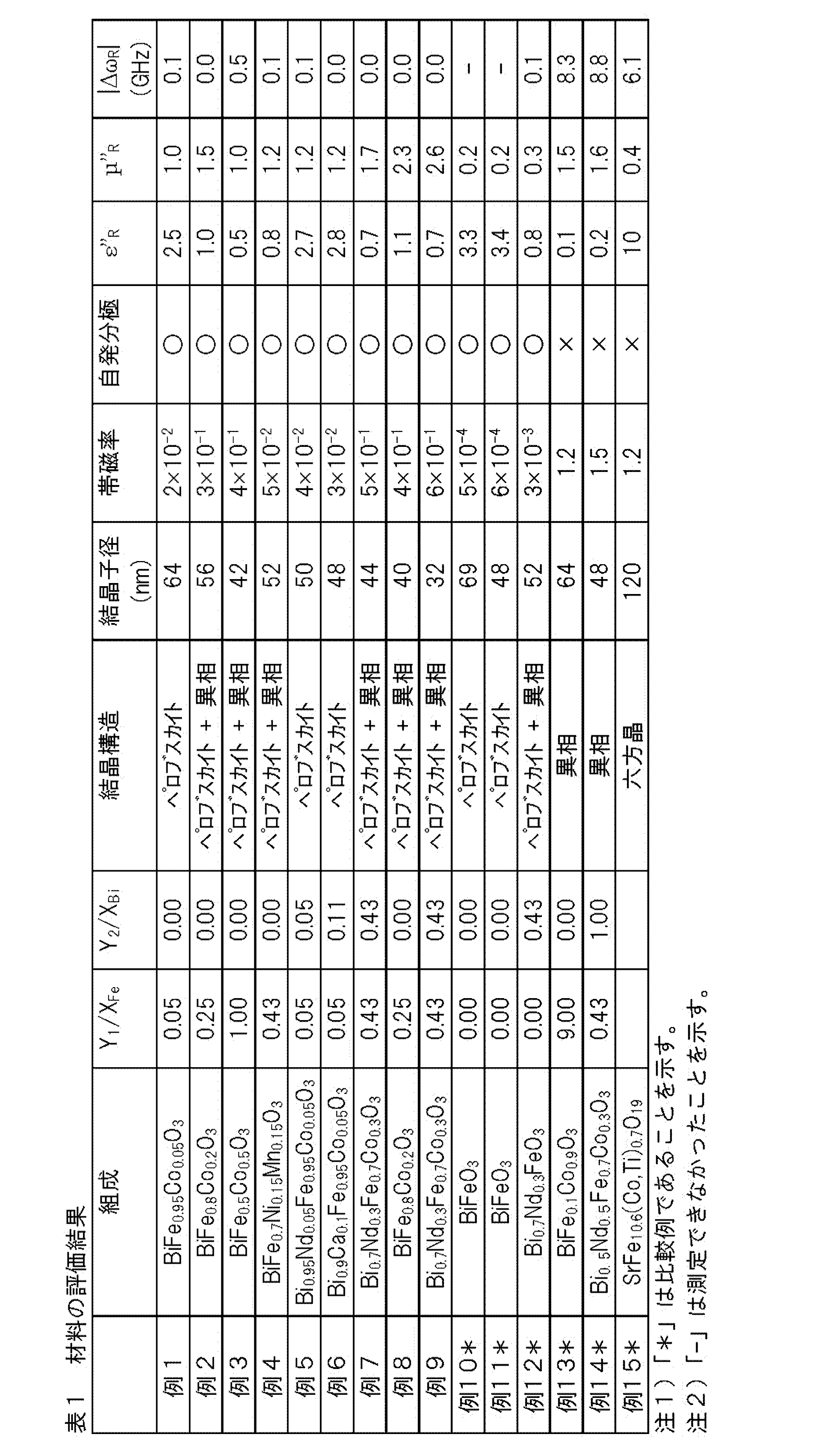
Claims (10)
- 電磁波吸収材料であって、
前記電磁波吸収材料がマルチフェロイック材料を含み、
前記マルチフェロイック材料が、ビスマス(Bi)及び鉄(Fe)を含み、さらにニッケル(Ni)、コバルト(Co)、マンガン(Mn)及びクロム(Cr)からなる群から選択される1種以上の第1添加元素を含む複合酸化物からなり、
前記複合酸化物が、ペロブスカイト(Perovskite)型構造、ダブルペロブスカイト(Double-Perovskite)型構造、ルデルスデンポッパー(Ruddlesden-Popper)型構造及びディオンジャコブソン(Dion-Jacobson)型構造からなる群から選択される1種以上の結晶構造を有し、
前記マルチフェロイック材料が吸収する電磁波の周波数は、100MHz以上1THz以下の範囲内にある、材料。 - 前記マルチフェロイック材料は、誘電損失ピーク周波数(ωE)及び磁気損失ピーク周波数(ωM)の両方が100MHz以上1THz以下の範囲内にある、請求項1に記載の材料。
- 鉄(Fe)のモル量(XFe)に対する第1添加元素の合計モル量(Y1)の比(Y1/XFe)が、0.00超4.00以下である、請求項1又は2に記載の材料。
- 前記複合酸化物が、亜鉛(Zn)、マグネシウム(Mg)、カルシウム(Ca)、ストロンチウム(Sr)、バリウム(Ba)、鉛(Pb)、希土類元素(RE)、チタン(Ti)、ニオブ(Nb)、ジルコニウム(Zr)、アルミニウム(Al)、銅(Cu)及びタンタル(Ta)からなる群から選択される1種以上の第2添加元素をさらに含む、請求項1~3のいずれか一項に記載の材料。
- 前記複合酸化物中のビスマス(Bi)のモル量(XBi)に対する亜鉛(Zn)、マグネシウム(Mg)、カルシウム(Ca)、ストロンチウム(Sr)、バリウム(Ba)、鉛(Pb)、希土類元素(RE)、チタン(Ti)、ニオブ(Nb)、ジルコニウム(Zr)、アルミニウム(Al)、銅(Cu)及びタンタル(Ta)からなる群から選択される1種以上の第2添加元素の合計モル量(Y2)の比(Y2/XBi)が、0.00以上0.80以下である、請求項1~4のいずれか一項に記載の材料。
- 前記電磁波吸収材料が、粉末、成形体又は焼結体である、請求項1~5のいずれか一項に記載の材料。
- 請求項1~6のいずれか一項に記載の材料を含有する、電磁波吸収体。
- 前記電磁波吸収材料が粉末であり、該粉末と母材とからなり、該粉末が母材中に分散されてなる、請求項7に記載の電磁波吸収体。
- 前記母材が、有機物、高分子、ガラス及びセラミックスからなる群から選択される1種以上の材料からなる、請求項8に記載の電磁波吸収体。
- 前記電磁波吸収材料が焼結体である、請求項7に記載の電磁波吸収体。
Priority Applications (1)
| Application Number | Priority Date | Filing Date | Title |
|---|---|---|---|
| JP2020523826A JP6733857B1 (ja) | 2019-02-20 | 2019-12-26 | 電磁波吸収材料及び電磁波吸収体 |
Applications Claiming Priority (4)
| Application Number | Priority Date | Filing Date | Title |
|---|---|---|---|
| JP2019-028326 | 2019-02-20 | ||
| JP2019028326 | 2019-02-20 | ||
| JP2019077731 | 2019-04-16 | ||
| JP2019-077731 | 2019-04-16 |
Publications (1)
| Publication Number | Publication Date |
|---|---|
| WO2020170608A1 true WO2020170608A1 (ja) | 2020-08-27 |
Family
ID=72144676
Family Applications (1)
| Application Number | Title | Priority Date | Filing Date |
|---|---|---|---|
| PCT/JP2019/051314 Ceased WO2020170608A1 (ja) | 2019-02-20 | 2019-12-26 | 電磁波吸収材料及び電磁波吸収体 |
Country Status (2)
| Country | Link |
|---|---|
| JP (1) | JP6733857B1 (ja) |
| WO (1) | WO2020170608A1 (ja) |
Cited By (3)
| Publication number | Priority date | Publication date | Assignee | Title |
|---|---|---|---|---|
| CN113573561A (zh) * | 2021-06-16 | 2021-10-29 | 南京航空航天大学 | 一种钙钛矿型电磁波吸收材料及其制备方法 |
| CN117119778A (zh) * | 2023-08-30 | 2023-11-24 | 哈尔滨工程大学 | 一种mof基多相复合型电磁波吸收材料的制备方法 |
| CN119797903A (zh) * | 2025-01-06 | 2025-04-11 | 郑州大学 | 一种钙钛矿型陶瓷材料及其制备方法和应用 |
Families Citing this family (2)
| Publication number | Priority date | Publication date | Assignee | Title |
|---|---|---|---|---|
| KR20220026316A (ko) * | 2020-08-25 | 2022-03-04 | 현대자동차주식회사 | GHz 대역의 전자파 흡수입자 및 이를 포함하는 전자파 흡수재 |
| CN113436824B (zh) * | 2021-07-07 | 2024-08-16 | 上海圣石生物医学科技有限公司 | 磁性吸波材料、其制备方法、其应用及保健产品 |
Citations (1)
| Publication number | Priority date | Publication date | Assignee | Title |
|---|---|---|---|---|
| JP2016515298A (ja) * | 2013-02-21 | 2016-05-26 | スリーエム イノベイティブ プロパティズ カンパニー | 電磁干渉軽減特性を有するポリマー複合物 |
Family Cites Families (4)
| Publication number | Priority date | Publication date | Assignee | Title |
|---|---|---|---|---|
| JPH05283886A (ja) * | 1992-03-31 | 1993-10-29 | Riken Corp | 電波吸収体の製造方法 |
| JPH05283884A (ja) * | 1992-03-31 | 1993-10-29 | Riken Corp | 電波吸収体 |
| JPH06232583A (ja) * | 1993-02-04 | 1994-08-19 | Riken Corp | フェライト電波吸収体 |
| JP4153345B2 (ja) * | 2003-03-31 | 2008-09-24 | 独立行政法人科学技術振興機構 | SiC−六方晶フェライト系セラミックス複合型電磁波吸収体の製造方法 |
-
2019
- 2019-12-26 JP JP2020523826A patent/JP6733857B1/ja not_active Expired - Fee Related
- 2019-12-26 WO PCT/JP2019/051314 patent/WO2020170608A1/ja not_active Ceased
Patent Citations (1)
| Publication number | Priority date | Publication date | Assignee | Title |
|---|---|---|---|---|
| JP2016515298A (ja) * | 2013-02-21 | 2016-05-26 | スリーエム イノベイティブ プロパティズ カンパニー | 電磁干渉軽減特性を有するポリマー複合物 |
Cited By (3)
| Publication number | Priority date | Publication date | Assignee | Title |
|---|---|---|---|---|
| CN113573561A (zh) * | 2021-06-16 | 2021-10-29 | 南京航空航天大学 | 一种钙钛矿型电磁波吸收材料及其制备方法 |
| CN117119778A (zh) * | 2023-08-30 | 2023-11-24 | 哈尔滨工程大学 | 一种mof基多相复合型电磁波吸收材料的制备方法 |
| CN119797903A (zh) * | 2025-01-06 | 2025-04-11 | 郑州大学 | 一种钙钛矿型陶瓷材料及其制备方法和应用 |
Also Published As
| Publication number | Publication date |
|---|---|
| JP6733857B1 (ja) | 2020-08-05 |
| JPWO2020170608A1 (ja) | 2021-03-11 |
Similar Documents
| Publication | Publication Date | Title |
|---|---|---|
| JP6733857B1 (ja) | 電磁波吸収材料及び電磁波吸収体 | |
| Shirsath et al. | Co–Al-substituted strontium hexaferrite for rare earth free permanent magnet and microwave absorber application | |
| Lee et al. | Absorption-dominant mmWave EMI shielding films with ultralow reflection using ferromagnetic resonance frequency tunable M-type ferrites | |
| JP6733858B1 (ja) | 電磁波吸収材料及び電磁波吸収体 | |
| Ahmad et al. | Magnetic and microwave attenuation behavior of Al-substituted Co2W hexaferrites synthesized by sol-gel autocombustion process | |
| Ahmad et al. | Characterization of Sr-substituted W-type hexagonal ferrites synthesized by sol–gel autocombustion method | |
| Sözeri et al. | Magnetic and microwave properties of BaFe12O19 substituted with magnetic, non-magnetic and dielectric ions | |
| Gao et al. | Electromagnetic and microwave absorption properties of Ti doped Li–Zn ferrites | |
| Afghahi et al. | Single and double-layer composite microwave absorbers with hexaferrite BaZn0. 6Zr0. 3X0. 3Fe10. 8O19 (X= Ti, Ce, Sn) powders | |
| Nikmanesh et al. | Erbium-chromium substituted strontium hexaferrite particles: Characterization of the physical and Ku-band microwave absorption properties | |
| Narang et al. | Single-layer & double-layer microwave absorbers based on Co–Ti substituted barium hexaferrites for application in X and Ku-band | |
| Lee et al. | Tunable and broad-band electromagnetic wave absorption using W-type Hexaferrites in 1–40 GHz range | |
| Hojjati-Najafabadi et al. | Magneto-electric features of BaFe9. 5Al1. 5CrO19-CaCu3Ti4O12 nanocomposites | |
| Aggarwal et al. | X-Band Microwave Analysis and Characterization of Zinc Substituted Nickel Ferrites Prepared by Sol–Gel Citrate Route: Aggarwal and Narang | |
| Mahbub et al. | Structural, dielectric, and magnetic properties of Ba-doped multiferroic bismuth ferrite | |
| Xiong et al. | Enhanced X and Ku band microwave absorption powered by a magnetic–dielectric synergistic effect in Pr-doped M/W composite hexaferrites | |
| Ansaree et al. | Structural, dielectric and magnetic properties of particulate composites of relaxor (BaTi0. 85Sn0. 15O3) and ferrite (NiFe2O4) synthesized by gel-combustion method | |
| Gajula et al. | High frequency studies on dielectric, impedance and Nyquist properties of BaTiO3–Li0. 5Fe2. 5O4 composite ceramics substituted with Sm and Nb for microwave device applications | |
| Stergiou et al. | Rare earth substituted hexagonal ferrites for electromagnetic absorber applications. Recent advances and critical issues | |
| Khan et al. | Improved multiferroic and magnetodielectric properties in Ni and Fe co-doped barium strontium titanate ceramics | |
| Lei et al. | Mn-substituted Co2Z ferrite ceramics with impedance matching for ultra-high frequency miniaturization antennas | |
| Rajan et al. | Multiferroic and magneto-dielectric properties in Fe doped BaTiO3 | |
| Jamalian et al. | Sol–gel synthesis of Mn–Sn–Ti-substituted strontium hexaferrite nanoparticles: structural, magnetic, and reflection-loss properties | |
| Peng et al. | Magnetic and dielectric properties of low-temperature sintered NiCuZn/CaTiO3 composite dual-performance materials | |
| Karim et al. | Study of structural, dielectric, and magnetic properties of nickel doped strontium hexaferrite nanoparticles for microwave absorption application |
Legal Events
| Date | Code | Title | Description |
|---|---|---|---|
| ENP | Entry into the national phase |
Ref document number: 2020523826 Country of ref document: JP Kind code of ref document: A |
|
| 121 | Ep: the epo has been informed by wipo that ep was designated in this application |
Ref document number: 19916136 Country of ref document: EP Kind code of ref document: A1 |
|
| NENP | Non-entry into the national phase |
Ref country code: DE |
|
| 122 | Ep: pct application non-entry in european phase |
Ref document number: 19916136 Country of ref document: EP Kind code of ref document: A1 |