WO2020170408A1 - 荷電粒子線装置 - Google Patents
荷電粒子線装置 Download PDFInfo
- Publication number
- WO2020170408A1 WO2020170408A1 PCT/JP2019/006691 JP2019006691W WO2020170408A1 WO 2020170408 A1 WO2020170408 A1 WO 2020170408A1 JP 2019006691 W JP2019006691 W JP 2019006691W WO 2020170408 A1 WO2020170408 A1 WO 2020170408A1
- Authority
- WO
- WIPO (PCT)
- Prior art keywords
- filament
- time
- particle beam
- charged particle
- imaging
- Prior art date
- Legal status (The legal status is an assumption and is not a legal conclusion. Google has not performed a legal analysis and makes no representation as to the accuracy of the status listed.)
- Ceased
Links
Images



Classifications
-
- H—ELECTRICITY
- H01—ELECTRIC ELEMENTS
- H01J—ELECTRIC DISCHARGE TUBES OR DISCHARGE LAMPS
- H01J37/00—Discharge tubes with provision for introducing objects or material to be exposed to the discharge, e.g. for the purpose of examination or processing thereof
- H01J37/02—Details
- H01J37/04—Arrangements of electrodes and associated parts for generating or controlling the discharge, e.g. electron-optical arrangement or ion-optical arrangement
- H01J37/06—Electron sources; Electron guns
- H01J37/073—Electron guns using field emission, photo emission, or secondary emission electron sources
-
- H—ELECTRICITY
- H01—ELECTRIC ELEMENTS
- H01J—ELECTRIC DISCHARGE TUBES OR DISCHARGE LAMPS
- H01J37/00—Discharge tubes with provision for introducing objects or material to be exposed to the discharge, e.g. for the purpose of examination or processing thereof
- H01J37/02—Details
- H01J37/04—Arrangements of electrodes and associated parts for generating or controlling the discharge, e.g. electron-optical arrangement or ion-optical arrangement
- H01J37/06—Electron sources; Electron guns
-
- H—ELECTRICITY
- H01—ELECTRIC ELEMENTS
- H01J—ELECTRIC DISCHARGE TUBES OR DISCHARGE LAMPS
- H01J37/00—Discharge tubes with provision for introducing objects or material to be exposed to the discharge, e.g. for the purpose of examination or processing thereof
- H01J37/02—Details
- H01J37/22—Optical, image processing or photographic arrangements associated with the tube
- H01J37/222—Image processing arrangements associated with the tube
-
- H—ELECTRICITY
- H01—ELECTRIC ELEMENTS
- H01J—ELECTRIC DISCHARGE TUBES OR DISCHARGE LAMPS
- H01J37/00—Discharge tubes with provision for introducing objects or material to be exposed to the discharge, e.g. for the purpose of examination or processing thereof
- H01J37/02—Details
- H01J37/244—Detectors; Associated components or circuits therefor
-
- H—ELECTRICITY
- H01—ELECTRIC ELEMENTS
- H01J—ELECTRIC DISCHARGE TUBES OR DISCHARGE LAMPS
- H01J37/00—Discharge tubes with provision for introducing objects or material to be exposed to the discharge, e.g. for the purpose of examination or processing thereof
- H01J37/26—Electron or ion microscopes; Electron or ion diffraction tubes
- H01J37/261—Details
- H01J37/265—Controlling the tube; circuit arrangements adapted to a particular application not otherwise provided, e.g. bright-field-dark-field illumination
-
- H—ELECTRICITY
- H01—ELECTRIC ELEMENTS
- H01J—ELECTRIC DISCHARGE TUBES OR DISCHARGE LAMPS
- H01J2237/00—Discharge tubes exposing object to beam, e.g. for analysis treatment, etching, imaging
- H01J2237/06—Sources
- H01J2237/065—Source emittance characteristics
-
- H—ELECTRICITY
- H01—ELECTRIC ELEMENTS
- H01J—ELECTRIC DISCHARGE TUBES OR DISCHARGE LAMPS
- H01J2237/00—Discharge tubes exposing object to beam, e.g. for analysis treatment, etching, imaging
- H01J2237/244—Detection characterized by the detecting means
- H01J2237/2448—Secondary particle detectors
-
- H—ELECTRICITY
- H01—ELECTRIC ELEMENTS
- H01J—ELECTRIC DISCHARGE TUBES OR DISCHARGE LAMPS
- H01J2237/00—Discharge tubes exposing object to beam, e.g. for analysis treatment, etching, imaging
- H01J2237/245—Detection characterised by the variable being measured
- H01J2237/24592—Inspection and quality control of devices
-
- H—ELECTRICITY
- H01—ELECTRIC ELEMENTS
- H01J—ELECTRIC DISCHARGE TUBES OR DISCHARGE LAMPS
- H01J37/00—Discharge tubes with provision for introducing objects or material to be exposed to the discharge, e.g. for the purpose of examination or processing thereof
- H01J37/26—Electron or ion microscopes; Electron or ion diffraction tubes
- H01J37/28—Electron or ion microscopes; Electron or ion diffraction tubes with scanning beams
Definitions
- the present invention relates to a charged particle beam device that irradiates a sample with a charged particle beam.
- a filament is used as the charged particle beam source of the charged particle beam device.
- the charged particle beam source is an electron
- a thermoelectron generated when a voltage is applied across the filament to heat the filament is used.
- An electron gun using this principle is called a thermionic gun.
- the filament life of a thermoelectron gun is generally as short as about 50 to 100 hours, and it can be understood that the filament life of a Schottky electron gun is frequently cut off considering that it is 1 to 2 years. Therefore, if the filament is continuously operated during long-term observation/analysis, the risk that the filament will break during observation increases.
- the filament breaks in the middle of long-time imaging, it is necessary to search the field of view of the observation sample again, focus adjustment, and perform imaging again, and thus the utilization efficiency of the device deteriorates. It is possible to replace the filament with a new one before the observation so that it will not be cut during the imaging, but more filaments will be used, leading to an increase in running cost.
- Patent Document 1 discloses a technique for preventing an unexpected downtime due to the life of the electron source in an electron beam apparatus using a Schottky electron source and replacing the electron source or the electron gun at an optimum time.
- the allowable usage time of the electron source is set in advance, and the remaining life time is calculated based on the allowable usage time and the cumulative usage time.
- the present invention has been made in view of the above problems, and reduces the possibility of needing to re-measure the filament break during observation, reduce the running cost of the device, improve the device operating efficiency The purpose is to let.
- the charged particle beam apparatus calculates the imaging time required to generate an observation image of a sample, estimates the remaining usable time of the filament, and when the imaging time is longer than the remaining usable time. Presents that fact.
- the charged particle beam device of the present invention it is possible to suppress the possibility of filament breakage during observation. This can prevent an unexpected downtime due to the life of the charged particle source and replace the electron source or the electron gun at an optimum time. Therefore, the running cost of the device can be reduced and the operating efficiency of the device can be improved.
- FIG. 1 is a configuration diagram of a scanning electron microscope 100 according to the first embodiment. It is an example of a method of capturing an observation image of a wide area. It is an example of a GUI displayed by the display device 103.
- 3 is a functional block diagram showing the configuration of a computer 126.
- FIG. 6 is a graph illustrating the change over time in the electrical resistance of the filament 125. 6 is a flowchart illustrating an operation procedure of the scanning electron microscope 100.
- FIG. 1 is a configuration diagram of a scanning electron microscope 100 according to the first embodiment of the present invention.
- the scanning electron microscope 100 includes a lens barrel section 101, a sample chamber 102, a control section 117, a computer 126, and a display device 103.
- the lens barrel 101 has a cathode 106, a Wehnelt 107, a filament 125, an anode 109, a first focusing lens 110, a second focusing lens 111, an upper deflection coil 112, a lower deflection coil 113, and an objective lens 114.
- the sample chamber 102 is maintained at a vacuum degree of 10 ⁇ 3 to 10 ⁇ 4 Pa by a vacuum pump 105.
- the sample chamber 102 has a sample 115, a sample stage 116, a sample stage 127, and a detector 104.
- the control unit 117 is a functional unit that controls each unit included in the scanning electron microscope 100, and includes a high voltage control circuit 119, a focusing lens control circuit 120, a deflection control circuit 121, an objective lens control circuit 122, and a signal processing circuit 123.
- the high voltage control circuit 119 controls the voltage applied to the electron gun 118.
- the focusing lens control circuit 120 controls the first focusing lens 110 and the second focusing lens 111.
- the deflection control circuit 121 controls the upper deflection coil 112 and the lower deflection coil 113.
- the objective lens control circuit 122 controls the objective lens 114.
- the high voltage control circuit 119 applies a desired voltage to the filament 125, the Wehnelt 107, and the anode 109 in the electron gun 118. By applying a voltage, the primary electron beam 108 is emitted from the filament 125.
- the electron gun 118 can be configured as a thermoelectron gun that emits the primary electron beam 108 by utilizing thermoelectrons generated by heating the filament 125, for example.
- the primary electron beam 108 is focused by the first focusing lens 110 and the second focusing lens 111, and then focused on the sample 115 by the objective lens 114. At the same time, the primary electron beam 108 focused on the sample 115 is scanned by the upper deflection coil 112 and the lower deflection coil 113 at the irradiation position on the sample 115. Along with the irradiation of the primary electron beam 108, signal electrons are emitted from the sample 115 depending on the shape and composition of the sample 115.
- the detector 104 detects the signal electron.
- the detected signal electrons are amplified by the amplifier 124 and output to the computer 126 via the signal processing circuit 123.
- the computer 126 generates an observation image of the sample 115 using the detection result of the signal electrons, and the display device 103 displays the observation image.
- the scanning time per pixel is about several tens ns to several hundreds ⁇ s.
- a method of capturing such a wide area there are a method of increasing the number of pixels included in one image, a method of capturing a plurality of images while moving the sample stage 127 little by little, and joining them. ..
- the former method narrows the scanning interval of the primary electron beam 108 and widens the imaging area.
- the maximum number of pixels is limited by the memory of the computer, so the image size is limited. Therefore, generally, as in the latter method, the number of pixels to be imaged at one time and the visual field range of the image are adjusted to the observation object, and a plurality of images are imaged and attached while moving the sample stage 127.
- the user can automatically image the designated observation region by setting the observation region and the observation conditions in advance. Therefore, it is possible to automatically obtain a desired observation image for a long time without a person monitoring the imaging process. Of course, it is possible to combine both methods.
- the filament 125 When observing or analyzing a wide area, it may be necessary to operate the scanning electron microscope 100 continuously for a long time in some cases.
- the filament 125 has a life, and when the life of the filament 125 is reached, observation cannot be continued.
- the life of the filament 125 differs depending on the type of the electron gun 118, and when a tungsten filament is used, it depends on the conditions, but is generally said to be about 50 to 100 hours.
- the life of the filament 125 needs to be longer than the observation time. If the life of the filament 125 is shorter than the observation time, the filament 125 is cut during the observation, and the user needs to replace the filament 125 and perform the observation again, or restart the observation from the point where the observation is interrupted. ..
- the first embodiment enables the user to determine whether or not to continue the observation in accordance with the state of the filament 125 and the set observation condition in such a situation. Aim to improve running costs.
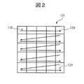
- Fig. 2 is an example of a method of capturing an observation image of a wide area.
- the user specifies the measurement range 131, and the imaging direction 130 starts from the measurement start position 128 and scans the primary electron beam 108 from left to right.
- the scanning position reaches the right end of the measurement range 131, the scanning position is moved to the next lower pixel line. The above procedure is repeated until the measurement end position 129.
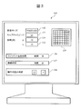
- FIG. 3 is an example of a GUI (Graphical User Interface) displayed by the display device 103.
- the user inputs the image size 132 and the capture speed 133 of the observed image.
- the number of picked-up images 134 in the X direction and the number of picked-up images 135 in the Y direction are designated.
- only one observation image is captured, it is sufficient to use only one XY image.
- the captured image 139 is an image of the sample 115 captured in advance.
- the user specifies a range to be captured by the scanning electron microscope 100 on the captured image 139. If the user can specify the imaging range, the captured image 139 may be an optically captured image or a scanning electron microscope image.
- the observation range is specified by (a) the user enclosing the desired imaging range with a figure, and (b) the user specifies the measurement start position 128 and the measurement end position 129 and determines the imaging range from the coordinates. It can be specified by If there is no captured image 139, the user may specify the measurement start position 128 and the measurement end position 129 by moving the sample stage 127 while displaying the observation image acquired by the scanning electron microscope 100 on the GUI. Multiple imaging ranges may be designated.
- the filament life time 136 displays the result of the computer 126 estimating the life of the filament 125 (remaining time until it can be used normally).
- the imaging time 137 displays the result of the computer 126 calculating the time required to acquire the observation image of the sample 115 according to the parameter specified on the GUI.
- the determination result 138 indicates the result of the determination made by the computer 126 according to the flowchart described later as to whether or not the entire captured image can be acquired.
- FIG. 4A is a functional block diagram showing the configuration of the computer 126.
- the computer 126 includes a comparison unit 144, a filament life estimation unit 149, an imaging time calculation unit 150, and a storage unit 145.
- the comparison unit 144/filament life estimation unit 149/imaging time calculation unit 150 can be configured by using hardware such as a circuit device having the function, or the arithmetic unit executes software having the function. It can also be configured as described above.
- the storage unit 145 can be configured by a storage device such as a hard disk. The operation of the comparison unit 144 will be described later.
- the filament life estimation unit 149 includes a timer 140, a current reading unit 141, an energization time recording unit 142, and a life calculation unit 143.
- the timer 140 counts the time when the filament 125 is energized.
- the current reading unit 141 reads the current value flowing through the filament 125 from, for example, an ammeter (not shown).
- the energization time recording unit 142 integrates the energization time counted by the timer 140 and stores the integrated energization time in the storage unit 145.
- the life calculation unit 143 calculates the life of the filament 125 by the method described later. The calculation result is used as the estimated life of the filament 125.
- the imaging time calculation unit 150 includes a time calculation unit 146, a time recording unit 147, and a setting reading unit 148.
- the setting reading unit 148 acquires the image size 132/capture speed 133/the number of captured images 134/the number of captured images 135 set by the user on the GUI described in FIG.
- the time recording unit 147 integrates the time when the scanning electron microscope 100 captured the observation image of the sample 115, and stores the integrated time in the storage unit 145.
- the time calculation unit 146 calculates the time required to capture an observation image of the sample 115 by the method described below.
- the total life time from the start of using the filament 125 to the time when it cannot be used normally is empirically obtained in advance, and the total life time is stored in the storage unit 145.
- the energization time recording unit 142 stores the accumulated energization time after the filament 125 is replaced with a new one in the storage unit 145.
- the life calculation unit 143 calculates the remaining usable time of the filament 125 by obtaining the difference between the life time stored in the storage unit 145 and the integrated energization time.
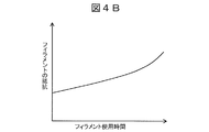
- FIG. 4B is a graph illustrating the change over time in the electrical resistance of the filament 125.
- the filament 125 is used at a high temperature and sublimes as the usage time is integrated. Therefore, the thickness of the filament 125 gradually changes. As a result, the electric resistance of the filament 125 changes with time.
- Data representing the change over time illustrated in FIG. 4B is stored in the storage unit 145 in advance.
- the life calculation unit 143 calculates the remaining usable time of the filament 125 by acquiring the electric resistance value of the filament 125 and referring to the data of FIG. 4B using the electric resistance value.
- the lifetime can also be calculated by combining the above methods. For example, it is conceivable to calculate the life using each of the two methods and calculate the life by weighting and adding each. Both methods may be combined by other suitable methods.
- the scan time is the number of pixels of the observed image ⁇ capture speed ⁇ total number of images.
- the number of pixels can be obtained from the image size 132.
- the capture speed is the irradiation time of the charged particle beam required to image one pixel. It can be obtained from the capture speed 133 on the GUI.
- the same portion on the observed image may be imaged a plurality of times and the images obtained by the respective imaging may be superimposed.
- the number of superposed sheets at this time is called an integrated number.
- the stage movement amount for one field of view can be known depending on how many divisions are made in the imaging region, and thus the time required to move the movement amount can be used as the stage movement time.
- FIG. 5 is a flowchart explaining the operation procedure of the scanning electron microscope 100. Each step of FIG. 5 will be described below.
- the filament life estimation unit 149 calculates an estimated life time T FIL of the filament and displays it on the filament life time 136.
- the image capturing time calculation unit 150 calculates the image capturing time T CAPT required to capture the observation image, and displays it on the image capturing time 137.
- the user or the comparison unit 144 determines whether or not the entire imaging range can be imaged by comparing T FIL and T CAPT (S501). When the comparison unit 144 makes a determination, the result is presented on the determination result 138. When the user makes a judgment, the result is input to the judgment result 138. If the entire imaging range can be imaged, the imaging is performed (S502), and the present flowchart ends. If the entire image capturing range cannot be captured, the process proceeds to step S503.
- Step S501 Supplement
- T FIL >T CAPT the process proceeds to step S502. If T FIL ⁇ T CAPT , the process advances to step S502 and a caution message is presented to the user. If T FIL ⁇ T CAPT , the process proceeds to step S503.
- Step S502 Supplement
- the user may be notified of a message indicating that imaging is possible on the GUI by characters or symbols.
- Fig. 5 Steps S503 to S505
- the computer 126 prompts the user to specify, on the GUI, whether to take an image until the filament 125 is cut or to replace the filament 125 with a new one and then start the image pickup (S503).
- the replacement S504: photographing
- the replacement work is performed (S505), and the present flowchart ends. If the user selects imaging, the process proceeds to step S506.
- Steps S506 to S508 The scanning electron microscope 100 continues imaging until the filament 125 is broken (S506).
- the computer 126 displays a message on the GUI prompting the filament 125 to be replaced (S507).
- the user replaces the filament 125 (S508).
- Step S506 Supplement
- Whether or not the filament 125 is broken can be determined, for example, by monitoring the value of the current flowing through the filament 125 and determining that the wire is broken when the current value becomes less than the determination threshold value. Alternatively, the determination may be made by an appropriate method.
- the control unit 117 stops the imaging operation when the filament 125 is broken.
- the scanning electron microscope 100 automatically determines whether or not the filament is cut during long-time observation before performing long-time observation, and notifies the user of the fact that the filament is cut halfway and re-established. It is possible to reduce the time and effort required for measurement and to start imaging with peace of mind.
- the user can change the observation conditions that were originally planned by viewing the life time of the filament and set in advance the condition that the imaging can be completed without the filament being cut, so that the filament can be used to the maximum extent.
- the setting condition capable of imaging in S503 can be presented to the user on the GUI.
- the second embodiment of the present invention a specific example thereof will be presented.
- the obtained filament life time T FIL is compared with the imaging time T CAPT . If T FIL ⁇ T CAPT or T FIL ⁇ T CAPT , the filament 125 is likely to be cut during the observation. At this time, if attention is paid or filament replacement is prompted as in the first embodiment, the filament 125 will be replaced even though the filament 125 can be used for some time, resulting in extra replacement cost for the user. Become. In view of this, in the second embodiment of the present invention, setting conditions that allow imaging within the range of the estimated filament life time are presented on the GUI.
- the observation range that can be imaged within the estimated filament life time range is presented to the user, and the user can set an arbitrary place within the observation range.
- the computer 126 arbitrarily changes (a) the number of images in each of the XY directions, (b) the scan speed, (c) the image size, (d) the number of images, and other parameters relating to the imaging time.
- several conditions that can be imaged within the filament life time are presented. At this time, the user may fix any of the parameters. In that case, the computer 126 presents the setting conditions that allow imaging while changing the other parameters.
- the user can maximize the life of the filament 125, so that the running cost required for the filament 125 can be reduced and the labor for exchanging the filament 125 can be reduced.
- the scanning electron microscope 100 calculates the maximum value of each condition using the filament life time before the user inputs the setting condition.
- the time required for automatic wide area observation can be roughly estimated (by multiplying these) according to the number of images taken, scan speed, total number of pixels, number of pixels, etc. Therefore, for example, if you want to find the maximum number of images that can be captured, substitute the minimum value that can be set for other parameters such as scan speed into the formula to estimate the maximum number of images that can be captured within the current filament life time. You can Other parameters can be calculated in the same manner, and when a certain parameter is set, each parameter is recalculated using the set value. Thereby, even when the user inputs each setting condition in an arbitrary order, it is possible to automatically set a condition in which imaging can be performed within the filament life time. Therefore, the labor required for the user to set the conditions can be reduced as compared with the second embodiment.
- the present invention can be applied to other types of charged particle beam devices. That is, if the charged particle beam device uses the filament 125 as a charged particle beam source, the present invention can be used to present the comparison result of the remaining life of the filament 125 and the imaging time on the GUI.
Landscapes
- Chemical & Material Sciences (AREA)
- Analytical Chemistry (AREA)
- Engineering & Computer Science (AREA)
- Computer Vision & Pattern Recognition (AREA)
- Analysing Materials By The Use Of Radiation (AREA)
Abstract
本発明は、観察途中においてフィラメントが切れて再測定する必要が生じる可能性を減らすとともに、装置のランニングコストを低減させ、装置稼働効率を向上させることを目的とする。本発明に係る荷電粒子線装置は、試料の観察画像を生成するために要する撮像時間を算出するとともに、フィラメントの残り使用可能時間を推定し、前記撮像時間が前記残り使用可能時間よりも長い場合は、その旨を提示する(図3参照)。
Description
本発明は、試料に対して荷電粒子線を照射する荷電粒子線装置に関する。
荷電粒子線装置の荷電粒子線源としてフィラメントが用いられる。例えば荷電粒子線源が電子である場合、フィラメント両端に電圧を印加し、フィラメントを加熱したときに発生する熱電子を用いる。この原理を用いた電子銃は熱電子銃と呼ばれる。この手法においては、フィラメントは高温化で使用されるので、昇華により使用にともなってフィラメントが損耗し、損耗が激しくなると断線してしまう。熱電子銃のフィラメント寿命時間は、一般的に50から100時間程度と短く、ショットキー型電子銃におけるフィラメントの寿命時間が1から2年であることを考えると頻繁に切れることが分かる。したがって、長時間観察・分析などにおいてフィラメントを連続稼働すると、フィラメントが観察中に切れてしまうリスクが高くなる。長時間撮像においてフィラメントが途中で断線すると、再度観察試料の視野探しやフォーカス調整などを実施して撮像しなおす必要があるので、装置の利用効率が悪くなってしまう。撮像途中で切れないように観察前に新品のフィラメントに交換することもできるが、より多くのフィラメントを使用することになり、ランニングコストを増大させる原因につながる。
下記特許文献1は、ショットキー電子源を使用した電子線装置において、電子源寿命による不意なダウンタイムを防ぎ、電子源または電子銃を最適な時期に交換するための技術を開示している。同文献においては、電子源の使用許容時間をあらかじめ設定しておき、その使用許容時間と積算使用時間に基づいて残り寿命時間を算出する。
特許文献1においては、使用許容時間と積算使用時間を比較する。しかしこの使用許容時間はユーザが設定したものであるので、必ずしもフィラメントの寿命を正確に反映していない場合がある。またこの使用許容時間は必ずしも観察時間を反映していないので、観察途中においてフィラメントが切れてしまう可能性がある。
本発明は、上記のような課題に鑑みてなされたものであり、観察途中においてフィラメントが切れて再測定する必要が生じる可能性を減らすとともに、装置のランニングコストを低減させ、装置稼働効率を向上させることを目的とする。
本発明に係る荷電粒子線装置は、試料の観察画像を生成するために要する撮像時間を算出するとともに、フィラメントの残り使用可能時間を推定し、前記撮像時間が前記残り使用可能時間よりも長い場合は、その旨を提示する。
本発明に係る荷電粒子線装置によれば、観察途中においてフィラメントが切れる可能性を抑制することができる。これにより、荷電粒子源の寿命による不意なダウンタイムを防ぎ、電子源または電子銃を最適な時期に交換することができる。したがって装置のランニングコストを低減させ、装置稼働効率を向上させることができる。
<実施の形態1>
図1は、本発明の実施形態1に係る走査型電子顕微鏡100の構成図である。走査型電子顕微鏡100は、鏡筒部101、試料室102、制御部117、コンピュータ126、表示装置103、を備える。鏡筒部101は、陰極106、ウェーネルト107、フィラメント125、陽極109、第1集束レンズ110、第2集束レンズ111、上段偏向コイル112、下段偏向コイル113、対物レンズ114、を有する。試料室102は、真空ポンプ105によって10-3~10-4Paの真空度に保たれる。試料室102は、試料115、試料台116、試料ステージ127、検出器104、を有する。
図1は、本発明の実施形態1に係る走査型電子顕微鏡100の構成図である。走査型電子顕微鏡100は、鏡筒部101、試料室102、制御部117、コンピュータ126、表示装置103、を備える。鏡筒部101は、陰極106、ウェーネルト107、フィラメント125、陽極109、第1集束レンズ110、第2集束レンズ111、上段偏向コイル112、下段偏向コイル113、対物レンズ114、を有する。試料室102は、真空ポンプ105によって10-3~10-4Paの真空度に保たれる。試料室102は、試料115、試料台116、試料ステージ127、検出器104、を有する。
制御部117は、走査型電子顕微鏡100が備える各部を制御する機能部であり、高電圧制御回路119、集束レンズ制御回路120、偏向制御回路121、対物レンズ制御回路122、信号処理回路123、を有する。高電圧制御回路119は、電子銃118に対して印加する電圧を制御する。集束レンズ制御回路120は、第1集束レンズ110と第2集束レンズ111を制御する。偏向制御回路121は、上段偏向コイル112と下段偏向コイル113を制御する。対物レンズ制御回路122は、対物レンズ114を制御する。
高電圧制御回路119は、電子銃118内のフィラメント125、ウェーネルト107、および陽極109に対して所望の電圧を印加する。電圧印加によりフィラメント125より1次電子ビーム108が放出される。電子銃118は、例えばフィラメント125を加熱することにより発生する熱電子を利用して1次電子ビーム108を出射する熱電子銃として構成することができる。
1次電子ビーム108は、第1集束レンズ110と第2集束レンズ111によって集束された後、対物レンズ114によって試料115上に集束される。試料115上に集束される1次電子ビーム108は同時に、上段偏向コイル112と下段偏向コイル113によって試料115上に対する照射位置を走査される。1次電子ビーム108の照射にともなって、試料115からは試料115の形状や組成などによって決まる信号電子が放出される。検出器104はその信号電子を検出する。検出された信号電子は、増幅器124により増幅され、信号処理回路123を介してコンピュータ126へ出力される。コンピュータ126は、信号電子の検出結果を用いて試料115の観察画像を生成し、表示装置103はその観察画像を表示する。
近年、コンピュータ126の記憶領域の増大化や、処理能力の高速化によって、広領域の画像を高解像で取得する傾向にある。このような使用方法は、試料115内のある数10nm~数10μmオーダの物質や構造を数mm~数10mm程度の広い領域において観察する用途や、微小物質の分析などの用途で使用されている。一方、走査型電子顕微鏡100は1次電子ビーム108を走査して1画素分ずつの信号情報を取得するので、ある程度のS/Nレベルを有する観察画像を取得するためには、高解像・広領域の画像を取得する場合であっても、1画素分の走査時間を短くすることができない。一般的には1画素当たりの走査時間は、数10ns~数100μs程度である。例えば、1画素あたり10nm正方領域を10μsの走査時間で取得し、観察画像サイズが1mm正方である場合を考えると、観察画像全体を撮像するために要する時間は、1mm×1mm/(10nm×10nm)×10μs=100000s=27.8hとなり、非常に長い時間が必要である。
一般的にこのような広領域を撮像する方法として、1枚の画像に含まれる画素数を増やす方法、試料ステージ127を少しずつ動かしながら複数枚の画像を撮像してつなぎ合わせる方法、などがある。前者の方法は、1次電子ビーム108の走査間隔を細かくするとともに撮像領域を広くする。この方法は繋ぎ目のない綺麗な画像がとれる反面、最大画素数がコンピュータのメモリによって制限されるので、画像サイズが制限されてしまう。そのため一般的には後者の手法のように1回に撮像される画素数や画像の視野範囲を観察物に合わせておき、試料ステージ127を動かしながら複数枚撮像して張り合わせる手法がとられる。ユーザはあらかじめ観察領域や観察条件などを設定しておくことにより、指定した観察領域を自動的に撮像することができる。したがって、撮像過程を人が監視することなく長時間自動的に所望の観察画像を得ることができる。もちろん、両方の手法を組み合せることも可能である。
広領域を観察または分析する際、場合によっては長時間連続して走査型電子顕微鏡100を稼働させておく必要がある。一方、フィラメント125は有寿命であり、フィラメント125が寿命を迎えると観察を続行することができなくなる。フィラメント125の寿命は電子銃118の種類によって異なり、タングステンフィラメントを用いた場合は条件にも依るが、一般的に50~100時間程度と言われている。フィラメント125の寿命は観察時間より長い必要がある。フィラメント125の寿命が観察時間よりも短ければ、フィラメント125が観察途中で切れてしまい、ユーザはフィラメント125を交換して再度観察し、あるいは観察が途切れてしまったところから観察を再開する必要がある。
このような状況を防ぐため、長時間観察する際は前もって新しいフィラメントに交換してもよいが、より多くのフィラメントを使用することとなり、ランニングコストの増大につながる。本実施形態1はこのような状況において、フィラメント125の状態や設定される観察条件に応じて、ユーザが観察を継続するか否かを判断できるようにすることにより、装置の稼働率や装置のランニングコストの向上を図る。
図2は、広領域の観察画像を撮像する方法の例である。ユーザは測定範囲131を指定し、撮像方向130は測定開始位置128から開始して左から右へ向かって1次電子ビーム108を走査する。走査位置が測定範囲131の右端に達すると1つ下の画素ラインへ走査位置を移動する。以上の手順を測定終了位置129まで繰り返す。
図3は、表示装置103が表示するGUI(Graphical User Interface)の例である。ユーザは、観察画像の画像サイズ132とキャプチャスピード133を入力する。複数の観察画像を撮像して張り合わせる場合は、X方向における撮像枚数134とY方向における撮像枚数135を指定する。1つの観察画像のみ撮像する場合はXYともに1枚とすればよい。これらの値は、ユーザが所望の観察条件や撮像範囲に応じて、入力もしくは決められた選択肢から選択する。
撮像画像139は、あらかじめ撮像した試料115の画像である。ユーザは撮像画像139上で、走査型電子顕微鏡100によって撮像する範囲を指定する。ユーザが撮像範囲を指定することができれば、撮像画像139は光学的に撮像した画像でもよいし走査電子顕微鏡像でもよい。観察範囲の指定は、(a)ユーザが所望の撮像範囲を図形で囲むことにより指定する、(b)ユーザが測定開始位置128と測定終了位置129を指定し、その座標から撮像範囲を決める、などによって指定することができる。撮像画像139がない場合は、走査型電子顕微鏡100によって取得した観察画像をGUI上に表示しながら、試料ステージ127を動かして測定開始位置128と測定終了位置129をユーザが指定してもよい。撮像範囲は複数指定してもよい。
フィラメント寿命時間136は、コンピュータ126がフィラメント125の寿命(正常に使用することができるまでの残時間)を推定した結果を表示する。撮像時間137は、GUI上で指定したパラメータにしたがって試料115の観察画像を取得するために要する時間をコンピュータ126が算出した結果を表示する。判断結果138は、撮像画像全体を取得することができるか否かを後述するフローチャートにしたがってコンピュータ126が判断した結果を示す。
図4Aは、コンピュータ126の構成を示す機能ブロック図である。コンピュータ126は、比較部144、フィラメント寿命推定部149、撮像時間算出部150、記憶部145を備える。比較部144/フィラメント寿命推定部149/撮像時間算出部150は、その機能を実装した回路デバイスなどのハードウェアを用いて構成することもできるし、その機能を実装したソフトウェアを演算装置が実行することにより構成することもできる。記憶部145は例えばハードディスクなどの記憶装置によって構成することができる。比較部144の動作については後述する。
フィラメント寿命推定部149は、タイマ140、電流読取部141、通電時間記録部142、寿命算出部143を備える。タイマ140は、フィラメント125に対して通電した時間をカウントする。電流読取部141は、フィラメント125に流れる電流値を例えば電流計(図示せず)から読み取る。通電時間記録部142は、タイマ140がカウントした通電時間を積算し、記憶部145に対してその積算通電時間を格納する。寿命算出部143は、後述する手法によりフィラメント125の寿命を算出する。その算出結果をフィラメント125の推定寿命として用いる。
撮像時間算出部150は、時間算出部146、時間記録部147、設定読取部148を備える。設定読取部148は、図3で説明したGUI上でユーザが設定した画像サイズ132/キャプチャスピード133/撮像枚数134/撮像枚数135を取得する。時間記録部147は、走査型電子顕微鏡100が試料115の観察画像を撮像した時間を積算し、その積算時間を記憶部145に対して格納する。時間算出部146は、後述する手法により試料115の観察画像を撮像するために要する時間を算出する。
(フィラメント125の寿命算出方法その1)
フィラメント125を使用し始めてから正常に使用できなくなるまでの総寿命時間をあらかじめ経験的に求め、記憶部145にその総寿命時間を格納しておく。通電時間記録部142は、フィラメント125を新品に交換してからの積算通電時間を記憶部145に格納する。寿命算出部143は、記憶部145が格納している寿命時間と積算通電時間との間の差分を求めることにより、フィラメント125の残り使用可能時間を算出する。
フィラメント125を使用し始めてから正常に使用できなくなるまでの総寿命時間をあらかじめ経験的に求め、記憶部145にその総寿命時間を格納しておく。通電時間記録部142は、フィラメント125を新品に交換してからの積算通電時間を記憶部145に格納する。寿命算出部143は、記憶部145が格納している寿命時間と積算通電時間との間の差分を求めることにより、フィラメント125の残り使用可能時間を算出する。
(フィラメント125の寿命算出方法その2)
図4Bは、フィラメント125の電気抵抗の経時変化を例示するグラフである。フィラメント125は高温下で使用され、使用時間が積算するのにともなって昇華するので、フィラメント125の太さは徐々に変化する。これによりフィラメント125の電気抵抗は経過変化する。図4Bに例示する経時変化を表すデータをあらかじめ記憶部145に格納しておく。寿命算出部143は、フィラメント125の電気抵抗値を取得し、その電気抵抗値を用いて図4Bのデータを参照することにより、フィラメントの125の残り使用可能時間を算出する。
図4Bは、フィラメント125の電気抵抗の経時変化を例示するグラフである。フィラメント125は高温下で使用され、使用時間が積算するのにともなって昇華するので、フィラメント125の太さは徐々に変化する。これによりフィラメント125の電気抵抗は経過変化する。図4Bに例示する経時変化を表すデータをあらかじめ記憶部145に格納しておく。寿命算出部143は、フィラメント125の電気抵抗値を取得し、その電気抵抗値を用いて図4Bのデータを参照することにより、フィラメントの125の残り使用可能時間を算出する。
(フィラメント125の寿命算出方法その3)
上記方法を組み合わせて寿命を算出することもできる。例えば両方法それぞれを用いて寿命を計算し、それぞれ重み付け加算することによって寿命を算出することが考えられる。その他適当な方法によって両方法を組み合わせてもよい。
上記方法を組み合わせて寿命を算出することもできる。例えば両方法それぞれを用いて寿命を計算し、それぞれ重み付け加算することによって寿命を算出することが考えられる。その他適当な方法によって両方法を組み合わせてもよい。
時間算出部146は、下記式にしたがって観察画像を撮像するために要する時間を算出することができる:撮像時間=撮像枚数×(スキャン時間+ステージ移動時間+待ち時間)。スキャン時間は、観察画像の画素数×キャプチャスピード×積算枚数である。画素数は画像サイズ132から求めることができる。キャプチャスピードは、1画素を撮像するために必要な荷電粒子線の照射時間である。GUI上のキャプチャスピード133から得ることができる。SN比を向上させるなどの目的のために、観察画像上の同一箇所を複数回撮像し、各撮像によって得られた画像を重畳する場合がある。このときの重畳枚数を積算枚数と呼ぶ。撮像領域を何分割するかによって例えば1視野分のステージ移動量が分かるので、その移動量を移動させるのに必要な時間をステージ移動時間として用いることができる。
図5は、走査型電子顕微鏡100の動作手順を説明するフローチャートである。以下図5の各ステップについて説明する。
(図5:ステップS501~S502)
フィラメント寿命推定部149はフィラメントの推定寿命時間TFILを算出し、フィラメント寿命時間136上に表示する。撮像時間算出部150は観察画像を撮像するために要する撮像時間TCAPTを算出し、撮像時間137上に表示する。ユーザまたは比較部144は、TFILとTCAPTを比較することにより、撮像範囲全体を撮像することができるか否かを判定する(S501)。比較部144が判定した場合はその結果を判断結果138上に提示する。ユーザが判定した場合はその結果を判断結果138に対して入力する。撮像範囲全体を撮像できる場合は撮像を実施し(S502)、本フローチャートを終了する。撮像範囲全体を撮像できない場合はステップS503へ進む。
フィラメント寿命推定部149はフィラメントの推定寿命時間TFILを算出し、フィラメント寿命時間136上に表示する。撮像時間算出部150は観察画像を撮像するために要する撮像時間TCAPTを算出し、撮像時間137上に表示する。ユーザまたは比較部144は、TFILとTCAPTを比較することにより、撮像範囲全体を撮像することができるか否かを判定する(S501)。比較部144が判定した場合はその結果を判断結果138上に提示する。ユーザが判定した場合はその結果を判断結果138に対して入力する。撮像範囲全体を撮像できる場合は撮像を実施し(S502)、本フローチャートを終了する。撮像範囲全体を撮像できない場合はステップS503へ進む。
(図5:ステップS501:補足)
本ステップにおける判断基準としては例えば以下のようなものが考えられる。TFIL>TCAPTであればステップS502へ進む。TFIL≒TCAPTであればステップS502へ進むとともにユーザに対して注意喚起メッセージを提示する。TFIL<TCAPTであればステップS503へ進む。
本ステップにおける判断基準としては例えば以下のようなものが考えられる。TFIL>TCAPTであればステップS502へ進む。TFIL≒TCAPTであればステップS502へ進むとともにユーザに対して注意喚起メッセージを提示する。TFIL<TCAPTであればステップS503へ進む。
(図5:ステップS502:補足)
S501からS502へ進む際には、GUI上において、撮像が可能であることを示すメッセージを、文字や記号などによってユーザに対して知らせてもよい。
S501からS502へ進む際には、GUI上において、撮像が可能であることを示すメッセージを、文字や記号などによってユーザに対して知らせてもよい。
(図5:ステップS503~S505)
コンピュータ126は、GUI上において、フィラメント125が切れるまで撮像するか、それともフィラメント125を新しいものに交換してから撮像を開始するかを指定するように、ユーザに対して促す(S503)。ユーザが交換を選択した場合は(S504:撮影)交換作業を実施し(S505)、本フローチャートを終了する。ユーザが撮像を選択した場合はステップS506へ進む。
コンピュータ126は、GUI上において、フィラメント125が切れるまで撮像するか、それともフィラメント125を新しいものに交換してから撮像を開始するかを指定するように、ユーザに対して促す(S503)。ユーザが交換を選択した場合は(S504:撮影)交換作業を実施し(S505)、本フローチャートを終了する。ユーザが撮像を選択した場合はステップS506へ進む。
(図5:ステップS506~S508)
走査型電子顕微鏡100は、フィラメント125が断線するまで撮像を継続する(S506)。フィラメント125が断線したとき、コンピュータ126はGUI上において、フィラメント125を交換するよう促すメッセージを表示する(S507)。ユーザはフィラメント125を交換する(S508)。
走査型電子顕微鏡100は、フィラメント125が断線するまで撮像を継続する(S506)。フィラメント125が断線したとき、コンピュータ126はGUI上において、フィラメント125を交換するよう促すメッセージを表示する(S507)。ユーザはフィラメント125を交換する(S508)。
(図5:ステップS506:補足)
フィラメント125が断線したか否かは、例えばフィラメント125に流れる電流値を監視し、電流値が判定閾値未満になったとき断線したと判定することができる。その他適当な手法により判定してもよい。制御部117は、フィラメント125が断線した時点で撮像動作を停止する。
フィラメント125が断線したか否かは、例えばフィラメント125に流れる電流値を監視し、電流値が判定閾値未満になったとき断線したと判定することができる。その他適当な手法により判定してもよい。制御部117は、フィラメント125が断線した時点で撮像動作を停止する。
<実施形態1:まとめ>
本実施形態1に係る走査型電子顕微鏡100は、長時間観察を行う前に長時間観察中にフィラメントが切れるかどうかを自動的に判断して、ユーザに知らせることによってフィラメントが途中で切れて再測定する手間を減らすことができるとともに、安心して撮像を開始することができる。またユーザは、フィラメントの寿命時間をみて、当初予定していた観察条件を変えてフィラメントが切れずに撮像が終了できる条件に前もって設定することができるため、フィラメントを最大限に活用することができ、フィラメントを交換する手間を減らすとともに、装置のランニングコストを低減することができる。
本実施形態1に係る走査型電子顕微鏡100は、長時間観察を行う前に長時間観察中にフィラメントが切れるかどうかを自動的に判断して、ユーザに知らせることによってフィラメントが途中で切れて再測定する手間を減らすことができるとともに、安心して撮像を開始することができる。またユーザは、フィラメントの寿命時間をみて、当初予定していた観察条件を変えてフィラメントが切れずに撮像が終了できる条件に前もって設定することができるため、フィラメントを最大限に活用することができ、フィラメントを交換する手間を減らすとともに、装置のランニングコストを低減することができる。
<実施の形態2>
実施形態1において、撮像時間がフィラメント125の残寿命以上である場合、S503において撮像可能な設定条件をGUI上でユーザに対して提示することができる。本発明の実施形態2では、その具体例を提示する。
実施形態1において、撮像時間がフィラメント125の残寿命以上である場合、S503において撮像可能な設定条件をGUI上でユーザに対して提示することができる。本発明の実施形態2では、その具体例を提示する。
例えば、求めたフィラメント寿命時間TFILと撮像時間TCAPTを比較し、TFIL≒TCAPTもしくはTFIL<TCAPTである場合、観察途中にてフィラメント125が切れてしまう可能性が高い。このとき実施形態1のように、注意喚起やフィラメント交換を促すと、まだフィラメント125をいくらかの時間は使用できるのにフィラメントを交換することになるので、ユーザにとっては余分な交換コストがかかることとなる。そこで本発明の実施形態2においては、推測されたフィラメント寿命時間の範囲内で撮像可能な設定条件をGUI上で提示する。
具体的には、例えば推測したフィラメント寿命時間の範囲内で撮像可能な観察範囲をユーザに提示し、ユーザはその観察範囲内で任意の場所を設定することができる。コンピュータ126は、観察範囲以外にも、(a)XY方向それぞれの撮像枚数、(b)スキャンスピード、(c)画像サイズ、(d)積算枚数、など撮像時間に関わる各パラメータを任意に変更しながら、フィラメント寿命時間内に撮像できる複数の条件を提示する。このときユーザはいずれかのパラメータを固定してもよい。その場合、コンピュータ126はそれ以外のパラメータを変更しながら撮像可能な設定条件を提示する。
本実施形態2によれば、ユーザはフィラメント125の寿命を最大限活用することができるので、フィラメント125に要するランニングコストを低減し、フィラメント125を交換する手間を削減することができる。
<実施の形態3>
実施形態2では、フィラメント寿命が撮像時間以下である場合、フィラメント寿命時間内で撮像できる設定条件をGUI上で提示することを説明した。一方で、フィラメント寿命時間は各設定条件に関係なくあらかじめ求めることができる。また、撮像に要する各設定条件はある一定の範囲を有すると考えられる。そこで本発明の実施形態3に係る走査型電子顕微鏡100は、ユーザが設定条件を入力する前に、フィラメント寿命時間を用いて各条件の最大値を算出することとする。
実施形態2では、フィラメント寿命が撮像時間以下である場合、フィラメント寿命時間内で撮像できる設定条件をGUI上で提示することを説明した。一方で、フィラメント寿命時間は各設定条件に関係なくあらかじめ求めることができる。また、撮像に要する各設定条件はある一定の範囲を有すると考えられる。そこで本発明の実施形態3に係る走査型電子顕微鏡100は、ユーザが設定条件を入力する前に、フィラメント寿命時間を用いて各条件の最大値を算出することとする。
自動広域観察に必要な時間は、撮像枚数、スキャンスピード、積算枚数、画素数などにしたがって(これらを乗算することにより)概算できる。したがって例えば最大撮像枚数を求めたい場合は、他のスキャンスピードなどのパラメータにおける設定可能な最小値を計算式に代入することにより、現在のフィラメント寿命時間内で撮像可能な最大撮像枚数を概算することができる。他のパラメータも同様に計算することができ、あるパラメータが設定された場合は、その設定値を用いて各パラメータを再計算する。これにより、ユーザが各設定条件を任意の順番で入力した場合であっても、自動的にフィラメント寿命時間内で撮像可能な条件を設定できる。したがって、ユーザが条件を設定する際に要する手間を、実施形態2よりも少なくすることができる。
<本発明の変形例について>
以上の実施形態において、走査型電子顕微鏡100を例示したが、その他タイプの荷電粒子線装置においても、本発明を適用することができる。すなわち、フィラメント125を荷電粒子線源として用いる荷電粒子線装置であれば、本発明を用いてフィラメント125の残寿命と撮像時間の比較結果をGUI上に提示することができる。
以上の実施形態において、走査型電子顕微鏡100を例示したが、その他タイプの荷電粒子線装置においても、本発明を適用することができる。すなわち、フィラメント125を荷電粒子線源として用いる荷電粒子線装置であれば、本発明を用いてフィラメント125の残寿命と撮像時間の比較結果をGUI上に提示することができる。
100:走査型電子顕微鏡
101:鏡筒部
102:試料室
103:表示装置
104:検出器
105:真空ポンプ
106:陰極
107:ウェーネルト
108:電子ビーム
109:陽極
110:第1集束レンズ
111:第2集束レンズ
112:上段偏向コイル
113:下段偏向コイル
114:対物レンズ
115:試料
116:試料台
117:制御部
118:電子銃
119:高電圧制御回路
120:集束レンズ制御回路
121:偏向制御回路
122:対物レンズ制御回路
123:信号処理回路
124:増幅器
125:フィラメント
126:コンピュータ
127:試料ステージ
101:鏡筒部
102:試料室
103:表示装置
104:検出器
105:真空ポンプ
106:陰極
107:ウェーネルト
108:電子ビーム
109:陽極
110:第1集束レンズ
111:第2集束レンズ
112:上段偏向コイル
113:下段偏向コイル
114:対物レンズ
115:試料
116:試料台
117:制御部
118:電子銃
119:高電圧制御回路
120:集束レンズ制御回路
121:偏向制御回路
122:対物レンズ制御回路
123:信号処理回路
124:増幅器
125:フィラメント
126:コンピュータ
127:試料ステージ
Claims (8)
- 試料に対して荷電粒子線を照射する荷電粒子線装置であって、
フィラメントから前記荷電粒子線を照射する荷電粒子線源、
前記荷電粒子線が前記試料に衝突することにより生じる2次荷電粒子を検出する検出器、
前記検出器が検出した前記2次荷電粒子を用いて前記試料の画像を生成するコンピュータ、
を備え、
前記コンピュータは、前記画像を生成するために要する撮像時間を算出し、
前記コンピュータは、前記フィラメントを正常に使用することができる残り時間を推定し、
前記コンピュータは、前記撮像時間が前記残り時間よりも長い場合は、その旨を示すアラートを出力する
ことを特徴とする荷電粒子線装置。 - 前記コンピュータは、前記撮像時間が前記残り時間よりも長い場合は、前記アラートとして、前記フィラメントを正常に使用することができる時間内に前記画像を生成することができる撮像可能範囲を提示する
ことを特徴とする請求項1記載の荷電粒子線装置。 - 前記コンピュータは、
前記画像の撮像枚数、
前記画像の画素サイズ、
前記画像を1画素分撮影するために必要な前記荷電粒子線の照射時間、
前記画像の同一箇所について重畳して前記画像を撮像する積算枚数、
のうち少なくともいずれかを撮像条件パラメータとして指定する指定入力を受け取り、
前記コンピュータは、前記指定入力による指定にしたがって前記撮像時間を算出し、
前記コンピュータは、前記撮像時間が前記残り時間よりも長い場合は、前記撮像可能範囲として、前記フィラメントを正常に使用することができる時間内に撮像完了することができる前記撮像条件パラメータを提示する
ことを特徴とする請求項2記載の荷電粒子線装置。 - 前記コンピュータは、前記撮像時間が前記残り時間よりも長い場合は、前記撮像可能範囲に到達するまで前記画像を取得するか、それとも前記フィラメントを交換するかを選択するように促すユーザインターフェースを提示し、
前記コンピュータは、前記ユーザインターフェースを介して、前記撮像可能範囲に到達するまで前記画像を取得する旨を選択する指示を受け取った場合は、前記フィラメントが正常に使用できなくなるまで前記画像を生成する
ことを特徴とする請求項2記載の荷電粒子線装置。 - 前記コンピュータは、前記撮像時間が前記残り時間よりも長い場合は、前記フィラメントを正常に使用することができる時間内に撮像完了することができる範囲内で設定可能な各前記撮像条件パラメータの最大値を、前記撮像可能範囲として提示する
ことを特徴とする請求項3記載の荷電粒子線装置。 - 前記コンピュータは、前記フィラメントに流れる電流の測定値を取得し、
前記コンピュータは、前記電流の測定値が判定閾値未満に達したとき、前記フィラメントが正常に使用できなくなったと判定するとともに、前記フィラメントを交換するように促すメッセージを前記ユーザインターフェース上で提示する
ことを特徴とする請求項4記載の荷電粒子線装置。 - 前記荷電粒子線装置はさらに、前記フィラメントを正常に使用することができる総使用可能時間を記述したデータを格納する記憶部を備え、
前記コンピュータは、前記フィラメントに対して通電した積算時間を算出し、
前記コンピュータは、前記総使用可能時間と前記積算時間を比較することにより、前記残り時間を推定する
ことを特徴とする請求項1記載の荷電粒子線装置。 - 前記荷電粒子線装置はさらに、前記フィラメントの電気抵抗値と前記フィラメントの使用可能時間との間の関係を記述したデータを格納する記憶部を備え、
前記コンピュータは、前記フィラメントの電気抵抗値を算出し、
前記コンピュータは、前記算出した電気抵抗値を用いて前記データを参照することにより、前記残り時間を推定する
ことを特徴とする請求項1記載の荷電粒子線装置。
Priority Applications (3)
| Application Number | Priority Date | Filing Date | Title |
|---|---|---|---|
| PCT/JP2019/006691 WO2020170408A1 (ja) | 2019-02-22 | 2019-02-22 | 荷電粒子線装置 |
| US17/287,249 US11404237B2 (en) | 2019-02-22 | 2019-02-22 | Charged particle beam device |
| JP2021501242A JP7095174B2 (ja) | 2019-02-22 | 2019-02-22 | 荷電粒子線装置 |
Applications Claiming Priority (1)
| Application Number | Priority Date | Filing Date | Title |
|---|---|---|---|
| PCT/JP2019/006691 WO2020170408A1 (ja) | 2019-02-22 | 2019-02-22 | 荷電粒子線装置 |
Publications (1)
| Publication Number | Publication Date |
|---|---|
| WO2020170408A1 true WO2020170408A1 (ja) | 2020-08-27 |
Family
ID=72144849
Family Applications (1)
| Application Number | Title | Priority Date | Filing Date |
|---|---|---|---|
| PCT/JP2019/006691 Ceased WO2020170408A1 (ja) | 2019-02-22 | 2019-02-22 | 荷電粒子線装置 |
Country Status (3)
| Country | Link |
|---|---|
| US (1) | US11404237B2 (ja) |
| JP (1) | JP7095174B2 (ja) |
| WO (1) | WO2020170408A1 (ja) |
Cited By (1)
| Publication number | Priority date | Publication date | Assignee | Title |
|---|---|---|---|---|
| JP7586793B2 (ja) | 2021-09-02 | 2024-11-19 | 株式会社日立製作所 | 熱放出型電子銃及び荷電粒子ビーム装置 |
Families Citing this family (1)
| Publication number | Priority date | Publication date | Assignee | Title |
|---|---|---|---|---|
| US11404237B2 (en) * | 2019-02-22 | 2022-08-02 | Hitachi High-Tech Corporation | Charged particle beam device |
Citations (8)
| Publication number | Priority date | Publication date | Assignee | Title |
|---|---|---|---|---|
| JP2003036807A (ja) * | 2001-07-18 | 2003-02-07 | Hitachi Ltd | 電子顕微鏡の電子銃監視装置および方法 |
| JP2007227255A (ja) * | 2006-02-24 | 2007-09-06 | Shimadzu Corp | 電子線源装置 |
| JP2007250425A (ja) * | 2006-03-17 | 2007-09-27 | Mitsubishi Heavy Ind Ltd | 熱電子発生装置、フィラメント寿命予測方法、及びフィラメント寿命延長方法 |
| JP2009245725A (ja) * | 2008-03-31 | 2009-10-22 | Jeol Ltd | 電子ビーム発生装置 |
| US9633815B1 (en) * | 2016-02-10 | 2017-04-25 | ICT Integrated Circuit Testing Gesellschaft für Halbleiterprüftechnik mbH | Emitter for an electron beam, electron beam device and method for producing and operating an electron emitter |
| WO2017179137A1 (ja) * | 2016-04-13 | 2017-10-19 | 株式会社 日立ハイテクノロジーズ | 荷電粒子線装置 |
| JP2018173372A (ja) * | 2017-03-31 | 2018-11-08 | 松定プレシジョン株式会社 | X線検査装置及びx線検査方法 |
| WO2018217167A1 (en) * | 2017-05-25 | 2018-11-29 | National University Of Singapore | Cathode structure for cold field electron emission and method of fabricating the same |
Family Cites Families (3)
| Publication number | Priority date | Publication date | Assignee | Title |
|---|---|---|---|---|
| JP3700424B2 (ja) | 1998-11-27 | 2005-09-28 | 株式会社日立製作所 | 電子線装置 |
| US10529070B2 (en) * | 2017-11-10 | 2020-01-07 | Arcam Ab | Method and apparatus for detecting electron beam source filament wear |
| US11404237B2 (en) * | 2019-02-22 | 2022-08-02 | Hitachi High-Tech Corporation | Charged particle beam device |
-
2019
- 2019-02-22 US US17/287,249 patent/US11404237B2/en active Active
- 2019-02-22 WO PCT/JP2019/006691 patent/WO2020170408A1/ja not_active Ceased
- 2019-02-22 JP JP2021501242A patent/JP7095174B2/ja active Active
Patent Citations (8)
| Publication number | Priority date | Publication date | Assignee | Title |
|---|---|---|---|---|
| JP2003036807A (ja) * | 2001-07-18 | 2003-02-07 | Hitachi Ltd | 電子顕微鏡の電子銃監視装置および方法 |
| JP2007227255A (ja) * | 2006-02-24 | 2007-09-06 | Shimadzu Corp | 電子線源装置 |
| JP2007250425A (ja) * | 2006-03-17 | 2007-09-27 | Mitsubishi Heavy Ind Ltd | 熱電子発生装置、フィラメント寿命予測方法、及びフィラメント寿命延長方法 |
| JP2009245725A (ja) * | 2008-03-31 | 2009-10-22 | Jeol Ltd | 電子ビーム発生装置 |
| US9633815B1 (en) * | 2016-02-10 | 2017-04-25 | ICT Integrated Circuit Testing Gesellschaft für Halbleiterprüftechnik mbH | Emitter for an electron beam, electron beam device and method for producing and operating an electron emitter |
| WO2017179137A1 (ja) * | 2016-04-13 | 2017-10-19 | 株式会社 日立ハイテクノロジーズ | 荷電粒子線装置 |
| JP2018173372A (ja) * | 2017-03-31 | 2018-11-08 | 松定プレシジョン株式会社 | X線検査装置及びx線検査方法 |
| WO2018217167A1 (en) * | 2017-05-25 | 2018-11-29 | National University Of Singapore | Cathode structure for cold field electron emission and method of fabricating the same |
Cited By (1)
| Publication number | Priority date | Publication date | Assignee | Title |
|---|---|---|---|---|
| JP7586793B2 (ja) | 2021-09-02 | 2024-11-19 | 株式会社日立製作所 | 熱放出型電子銃及び荷電粒子ビーム装置 |
Also Published As
| Publication number | Publication date |
|---|---|
| US20210384003A1 (en) | 2021-12-09 |
| US11404237B2 (en) | 2022-08-02 |
| JPWO2020170408A1 (ja) | 2021-10-07 |
| JP7095174B2 (ja) | 2022-07-04 |
Similar Documents
| Publication | Publication Date | Title |
|---|---|---|
| JP4065847B2 (ja) | 試料像形成方法及び荷電粒子線装置 | |
| WO2003044821A1 (en) | Sample imaging method and charged particle beam system | |
| KR20180049099A (ko) | 다중 빔 주사 전자 현미경 검사 시스템에서의 초점 조정을 위한 방법 및 시스템 | |
| JP2013069951A (ja) | 欠陥観察方法及び欠陥観察装置 | |
| JP7095174B2 (ja) | 荷電粒子線装置 | |
| JP4832375B2 (ja) | 試料像形成方法及び荷電粒子線装置 | |
| JP6343508B2 (ja) | コントラスト・ブライトネス調整方法、及び荷電粒子線装置 | |
| CN103906472A (zh) | X射线摄像系统 | |
| US20100038534A1 (en) | Method of generating particle beam images using a particle beam apparatus | |
| US11877377B2 (en) | Method of setting a filament demand in an X-ray apparatus, controller, X-ray apparatus, control program and storage medium | |
| JP2010101907A (ja) | 試料像形成方法及び荷電粒子線装置 | |
| JP2011014303A (ja) | 荷電粒子ビーム装置のオートフォーカス画像判定方法、荷電粒子ビーム装置のオートフォーカス画像判定装置、荷電粒子ビーム装置、コンピュータプログラム及び記録媒体 | |
| JP2010182424A (ja) | 荷電粒子線の光軸調整方法、及び荷電粒子線装置 | |
| JP4408908B2 (ja) | 荷電粒子線装置 | |
| JP7174773B2 (ja) | 荷電粒子線装置の調整方法及び荷電粒子線装置システム | |
| JP7060722B2 (ja) | 荷電粒子線装置 | |
| JP5352261B2 (ja) | 走査形電子顕微鏡及びその画像保存フォーマットと画像再編集方法 | |
| JP4696097B2 (ja) | 試料像形成方法及び荷電粒子線装置 | |
| US20250316446A1 (en) | Method for operating a particle beam microscope, particle beam microscope and computer program product | |
| JP4863886B2 (ja) | 電子線応用装置および電子源の安定稼動状態判定方法 | |
| JP2016213054A (ja) | 画像処理装置、電子顕微鏡、および画像処理方法 | |
| JP2005235782A (ja) | 電子線分析方法 | |
| JP2006228748A (ja) | 電子顕微鏡 | |
| US11621145B2 (en) | Method for operating a particle beam microscope | |
| JP7068069B2 (ja) | 電子顕微鏡 |
Legal Events
| Date | Code | Title | Description |
|---|---|---|---|
| 121 | Ep: the epo has been informed by wipo that ep was designated in this application |
Ref document number: 19916079 Country of ref document: EP Kind code of ref document: A1 |
|
| ENP | Entry into the national phase |
Ref document number: 2021501242 Country of ref document: JP Kind code of ref document: A |
|
| NENP | Non-entry into the national phase |
Ref country code: DE |
|
| 122 | Ep: pct application non-entry in european phase |
Ref document number: 19916079 Country of ref document: EP Kind code of ref document: A1 |