WO2020165688A1 - パラメータ探索方法 - Google Patents
パラメータ探索方法 Download PDFInfo
- Publication number
- WO2020165688A1 WO2020165688A1 PCT/IB2020/050854 IB2020050854W WO2020165688A1 WO 2020165688 A1 WO2020165688 A1 WO 2020165688A1 IB 2020050854 W IB2020050854 W IB 2020050854W WO 2020165688 A1 WO2020165688 A1 WO 2020165688A1
- Authority
- WO
- WIPO (PCT)
- Prior art keywords
- parameter
- netlist
- model
- model parameter
- neural network
- Prior art date
- Legal status (The legal status is an assumption and is not a legal conclusion. Google has not performed a legal analysis and makes no representation as to the accuracy of the status listed.)
- Ceased
Links
Images










Classifications
-
- G—PHYSICS
- G06—COMPUTING OR CALCULATING; COUNTING
- G06N—COMPUTING ARRANGEMENTS BASED ON SPECIFIC COMPUTATIONAL MODELS
- G06N3/00—Computing arrangements based on biological models
- G06N3/02—Neural networks
- G06N3/08—Learning methods
-
- G—PHYSICS
- G06—COMPUTING OR CALCULATING; COUNTING
- G06F—ELECTRIC DIGITAL DATA PROCESSING
- G06F30/00—Computer-aided design [CAD]
- G06F30/20—Design optimisation, verification or simulation
- G06F30/27—Design optimisation, verification or simulation using machine learning, e.g. artificial intelligence, neural networks, support vector machines [SVM] or training a model
-
- G—PHYSICS
- G06—COMPUTING OR CALCULATING; COUNTING
- G06F—ELECTRIC DIGITAL DATA PROCESSING
- G06F18/00—Pattern recognition
- G06F18/20—Analysing
- G06F18/24—Classification techniques
- G06F18/241—Classification techniques relating to the classification model, e.g. parametric or non-parametric approaches
-
- G—PHYSICS
- G06—COMPUTING OR CALCULATING; COUNTING
- G06F—ELECTRIC DIGITAL DATA PROCESSING
- G06F30/00—Computer-aided design [CAD]
- G06F30/30—Circuit design
- G06F30/36—Circuit design at the analogue level
-
- G—PHYSICS
- G06—COMPUTING OR CALCULATING; COUNTING
- G06F—ELECTRIC DIGITAL DATA PROCESSING
- G06F30/00—Computer-aided design [CAD]
- G06F30/30—Circuit design
- G06F30/36—Circuit design at the analogue level
- G06F30/367—Design verification, e.g. using simulation, simulation program with integrated circuit emphasis [SPICE], direct methods or relaxation methods
-
- G—PHYSICS
- G06—COMPUTING OR CALCULATING; COUNTING
- G06N—COMPUTING ARRANGEMENTS BASED ON SPECIFIC COMPUTATIONAL MODELS
- G06N3/00—Computing arrangements based on biological models
- G06N3/02—Neural networks
- G06N3/04—Architecture, e.g. interconnection topology
- G06N3/042—Knowledge-based neural networks; Logical representations of neural networks
-
- G—PHYSICS
- G06—COMPUTING OR CALCULATING; COUNTING
- G06N—COMPUTING ARRANGEMENTS BASED ON SPECIFIC COMPUTATIONAL MODELS
- G06N3/00—Computing arrangements based on biological models
- G06N3/02—Neural networks
- G06N3/04—Architecture, e.g. interconnection topology
- G06N3/045—Combinations of networks
-
- G—PHYSICS
- G06—COMPUTING OR CALCULATING; COUNTING
- G06N—COMPUTING ARRANGEMENTS BASED ON SPECIFIC COMPUTATIONAL MODELS
- G06N3/00—Computing arrangements based on biological models
- G06N3/02—Neural networks
- G06N3/04—Architecture, e.g. interconnection topology
- G06N3/0499—Feedforward networks
-
- G—PHYSICS
- G06—COMPUTING OR CALCULATING; COUNTING
- G06N—COMPUTING ARRANGEMENTS BASED ON SPECIFIC COMPUTATIONAL MODELS
- G06N3/00—Computing arrangements based on biological models
- G06N3/02—Neural networks
- G06N3/08—Learning methods
- G06N3/09—Supervised learning
-
- G—PHYSICS
- G06—COMPUTING OR CALCULATING; COUNTING
- G06N—COMPUTING ARRANGEMENTS BASED ON SPECIFIC COMPUTATIONAL MODELS
- G06N3/00—Computing arrangements based on biological models
- G06N3/02—Neural networks
- G06N3/08—Learning methods
- G06N3/092—Reinforcement learning
Definitions
- One aspect of the present invention relates to a computer-aided semiconductor parameter learning method, classification method, selection method, or search method.
- one embodiment of the present invention is not limited to the above technical field.
- chemical synthesis parameter search and the like can be given as an example.
- one embodiment of the present invention relates to a computer.
- One aspect of the present invention relates to a computerized computerized parameter search method for a netlist.
- One aspect of the present invention relates to a parameter classification method capable of extracting model parameters from a data set of a semiconductor device, allowing a classification model to learn a set of model parameters, and classifying the model parameters by the classification model.
- One aspect of the present invention relates to a parameter selection method for selecting a model parameter suitable for a required characteristic of a target netlist by the parameter classification method.
- One aspect of the present invention relates to a parameter search method that searches using reinforcement learning so that a variable of a netlist given to a circuit simulator becomes an optimal candidate that satisfies the required characteristics of the netlist.
- the user creates a netlist that is circuit information for circuit design.
- circuit information (hereinafter referred to as a netlist) has different required characteristics depending on the operating environment.
- the user performs a simulation by using a circuit simulator in order to realize the required characteristics of the netlist.
- the user searches for optimum candidates of model parameters that satisfy the required characteristics of the netlist while updating the model parameters of the semiconductor devices included in the netlist.
- Patent Document 1 discloses a parameter adjustment device that uses a genetic algorithm for parameter adjustment of a physical model of a transistor.
- the model parameter of the semiconductor element satisfying the required characteristics of the netlist is not limited to one and there may be a plurality of model parameters.
- the user may determine the optimum value by extracting the parameter that satisfies the required characteristic. In other words, there is a problem that the user overlooks the existence of different model parameters that may satisfy the required characteristics more. Therefore, the determination of the simulation result of the circuit simulator has a problem depending on the experience value of the user.
- the required characteristics of the netlist may differ. For example, there is a circuit for low power consumption, a circuit that places importance on operating frequency, or a circuit that operates stably in a specified frequency band.
- the required characteristic of the netlist has a problem that the required characteristic cannot be satisfied when the model parameter is fixed.
- an object of one embodiment of the present invention is to provide a computer-based electronic netlist parameter search method.
- one embodiment of the present invention provides a parameter classification method capable of extracting model parameters from a data set of a semiconductor device, allowing a classification model to learn a set of model parameters, and classifying the model parameters by the classification model. Is one of the challenges.
- An object of one embodiment of the present invention is to provide a parameter search method in which a variable of a netlist given to a circuit simulator is searched using reinforcement learning so as to be an optimal candidate that satisfies the required characteristics of the netlist. ..
- One aspect of the present invention is a parameter search method using a classification model, a neural network, a parameter extraction unit, a circuit simulator, and a control unit.
- the parameter extraction unit has a step of supplying a data set of the semiconductor device.
- the parameter extraction unit has a step of extracting a model parameter of the semiconductor device.
- the circuit simulator has a step of performing a simulation using the first netlist and the model parameter and outputting a first output result.
- the classification model has the steps of learning the first output result, classifying the model parameters, and outputting the first model parameters.
- the control unit has a step of providing the circuit simulator with the second netlist and the second model parameter.
- the control unit includes a step of giving the neural network a first model parameter variable included in the second model parameter.
- the neural network has a step of calculating a first action value function Q from the first model parameter variable.
- the control unit has a step of updating the first model parameter variable to the second model parameter variable by the first action value function Q and outputting the third model parameter.
- the circuit simulator has a step of performing a simulation using the second netlist and the third model parameter and outputting a second output result.
- the control unit includes a step of determining the second output result by using the convergence condition given to the second netlist. There is a step of determining the second output result and setting a reward and updating the weighting factor of the neural network using the reward when the required characteristic of the second netlist is not satisfied.
- the second output result is determined, and when the required characteristics of the second netlist are satisfied, it can be determined that the first model parameter variable is the optimum candidate for the second netlist.
- One aspect of the present invention is a parameter search method using a classification model, a neural network, a parameter extraction unit, a circuit simulator, and a control unit.
- the parameter extraction unit has a step of providing the measurement data of the semiconductor device and a data set including process parameters.
- the parameter extraction unit has a step of extracting model parameters.
- the control unit has a step of providing a first netlist to the circuit simulator.
- the circuit simulator has a step of outputting a first output result using the model parameter and the first netlist.
- the classification model has a step of classifying the model parameter by learning the model parameter and the first output result, and outputting the first model parameter.
- the control unit has a step of providing the circuit simulator with the second netlist and the second model parameter.
- the control unit includes a step of giving the neural network a first model parameter variable included in the second model parameter.
- the neural network has a step of calculating a first action value function Q from the first model parameter variable.
- the control unit has a step of updating the first model parameter variable to the second model parameter variable by the first action value function Q and outputting the third model parameter.
- the circuit simulator has a step of performing a simulation using the second netlist and the third model parameter and outputting a second output result.
- the control unit includes a step of determining the second output result by using the convergence condition given to the second netlist.
- the second output result is determined, and when the required characteristics of the second netlist are not satisfied, the control unit sets a high reward when the second output result approaches the convergence condition, and the second output There is the step of setting a low reward if the result deviates from the convergence condition.
- the neural network has a step of calculating a second action value function Q using the second model parameter variable.
- the neural network has the step of updating the weighting factor of the neural network using the reward and the error calculated using the first action value function Q and the second action value function Q.
- the second output result is determined, and when the required characteristics of the second netlist are satisfied, it can be determined that the first model parameter variable is the optimum candidate for the second netlist.
- the first netlist preferably includes any one or more of an inverter circuit, a source follower circuit, and a source ground circuit.
- the number of first model parameter variables is two or more.
- the number of units in the output layer of the neural network is at least twice the number of model parameter variables.
- the first output result extracted using the first netlist preferably includes any one or more of a leak current, an output current, a signal rise time, and a signal fall time. ..
- the semiconductor element used in the first netlist is a transistor, and the transistor is preferably a parameter searching method having a metal oxide in the semiconductor layer.
- One aspect of the present invention can provide a computer-based electronic netlist parameter search method.
- one embodiment of the present invention provides a parameter classification method capable of extracting model parameters from a data set of a semiconductor device, allowing a classification model to learn a set of model parameters, and classifying the model parameters by the classification model.
- You can Alternatively, one aspect of the present invention can provide a parameter selection method for selecting a model parameter suitable for the required characteristics of the target netlist by the parameter classification method.
- one embodiment of the present invention can provide a parameter search system that searches using reinforcement learning so that the variables of the netlist given to the circuit simulator become optimal candidates that satisfy the required characteristics of the netlist.
- the effects of one aspect of the present invention are not limited to the effects listed above.
- the effects listed above do not prevent the existence of other effects.
- the other effects are the effects described in the following description and not mentioned in this item.
- the effects not mentioned in this item can be derived from the description such as the specification or the drawings by those skilled in the art, and can be appropriately extracted from these descriptions.
- one embodiment of the present invention has at least one of the effects listed above and/or other effects. Therefore, one embodiment of the present invention may not have the effects listed above in some cases.
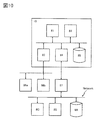
- FIG. 1 is a block diagram illustrating a parameter search method.
- FIG. 2 is a diagram illustrating a data set.
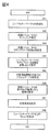
- FIG. 3 is a flowchart illustrating the parameter search method.
- FIG. 4 is a flowchart illustrating the parameter search method.
- FIG. 5 is a flowchart illustrating the parameter search method.
- FIG. 6 is a flowchart illustrating the parameter search method.
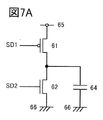
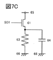
- 7A to 7D are diagrams for explaining the evaluation netlist.
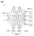
- FIG. 8 is a schematic diagram illustrating a neural network.
- FIG. 9 is a flowchart explaining the neural network.
- FIG. 10 is a block diagram illustrating a parameter search device having a parameter search method.
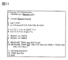
- FIG. 11 is a diagram for explaining a netlist describing an inverter circuit.
- FIG. 12 is a diagram illustrating a user setting file.
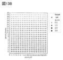
- FIG. 13A and FIG. 13B are diagrams for explaining search results of model parameters.
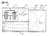
- 14A and 14B are diagrams illustrating a
- the parameter search method is controlled by the program running on the computer. Therefore, the computer can be paraphrased as a parameter search device including a parameter search method.
- the parameter search device will be described in detail with reference to FIG.
- the program is stored in the memory or storage of the computer. Alternatively, it is stored in a computer connected via a network (Local Area Network (LAN), Wide Area Network (WAN), Internet, etc.) or a server computer having a database.
- LAN Local Area Network
- WAN Wide Area Network
- Internet etc.
- server computer having a database.
- the parameter search method it is possible to search for an optimal parameter candidate using machine learning (Research) or reinforcement learning (Reinforcement Learning). It is preferable to use artificial intelligence (Artificial Intelligence (AI)) for part of the processing of machine learning or reinforcement learning.
- AI Artificial Intelligence
- an artificial neural network Artificial Neural Network (ANN), hereinafter simply referred to as a neural network
- ANN Artificial Neural Network
- the arithmetic processing of the neural network is realized by a circuit (hardware) or a program (software).
- a neural network refers to all models that determine the connection strength between neurons by learning and have problem solving ability.
- a neural network has an input layer, an intermediate layer (which may include multiple hidden layers), and an output layer.
- determining a connection strength (also called a weighting coefficient) between neurons from existing information may be referred to as “learning”.
- the classification model is generated by learning the model parameter of the semiconductor device.
- the classification model classifies model parameters.
- the model parameters are extracted by giving a data set (including measurement data or process parameters) of the semiconductor device to the parameter extraction unit.
- the classification suitable for the required characteristics of the netlist may not be sufficient with only the model parameter of the semiconductor device.
- the model parameter is further analyzed.
- a simulation by a circuit simulator is performed using the model parameter and the evaluation netlist given the model parameter.
- DC analysis, AC analysis, or transient analysis is performed using the evaluation netlist.
- the simulation result includes any one or more of the leakage current, the output current, the signal rise time, the signal fall time, and the like in the evaluation netlist.
- the model parameter and the result of the simulation using the evaluation netlist can be called learning content.
- a method in which the classification model performs learning by using the learning content is called a parameter learning method.
- the classification model should facilitate classification of a circuit that emphasizes low power consumption, a circuit that emphasizes operating frequency, or a circuit that operates stably in a specified frequency band, which could not be sufficiently performed by the parameter extraction unit alone. You can In order to simplify the description, the low power consumption required for the circuit, the operating frequency, or the stability in the frequency band may be described as the required characteristic.
- the classification model can present a plurality of candidates from the model parameters learned in the past. Further, it is possible to present a plurality of candidates from learned model parameters in an arbitrarily designated range.
- the classification model can present the fitness of the required characteristics of the new model parameter with probability. Thus, the user can obtain information for determining how suitable the new model parameters are for each required characteristic.
- the classification model can provide a parameter selection method capable of selecting a model parameter suitable for the required characteristic from the model parameters already learned. It should be noted that required characteristics may be added to the learning content.
- classification models described above include machine learning algorithms such as decision trees, naive Bayes, K Nearest Neighbor (KNN), Support Vector Machine (SVM), perceptron, or logistic regression, or neural networks, which are characterized by class classification. Can be used.
- machine learning algorithms such as decision trees, naive Bayes, K Nearest Neighbor (KNN), Support Vector Machine (SVM), perceptron, or logistic regression, or neural networks, which are characterized by class classification. Can be used.
- classification models may be generated.
- a classification model for clustering can be generated using the model parameter and the result of the simulation using the evaluation netlist.
- a machine learning algorithm such as K-means or density-based spatial clustering of applications with noise (BSCAN) can be used.
- Random sampling or cross variation can be used as a method for the classification model to select the content for learning.
- the learning content corresponds to the data set of the semiconductor device.
- the generated classification model can be saved in the main body of the electronic device or in an external memory, and may be called and used when classifying a new file.
- the classification model can be updated according to the method described.
- Q learning Q-learning
- Monte Carlo method Monte Carlo method
- Q-learning is a method for learning the value of an agent selecting action a t under a certain environment (represented as a variable s t ) at time t.
- Agent refers to entities to act, it refers to a subject that is variable s t is encouraged. Due to the action a t of the agent, a certain environment transits from the variable s t to the variable s t+1 , and the agent receives the reward r t+1 .
- the action a t is learned so that the total amount of rewards to be obtained finally becomes maximum.
- the value that the action a t in the variable s t, action-value function Q (s t, a t) can be expressed as.
- the update expression of the action value function Q(s t , a t ) can be expressed by Expression (1).
- the agent corresponds to the control unit
- the certain environment corresponds to the variable s t given to the input layer of the neural network
- the action a t is output by the agent to the output layer of the neural network. Determined by the action value function Q(s t , a t ).
- ⁇ indicates a learning rate ( ⁇ is greater than 0 and 1 or less), and ⁇ is a discount rate ( ⁇ is 0 or more and 1 or less).
- the learning rate ⁇ indicates whether to emphasize the present value or the result obtained by the action. The closer the learning rate ⁇ is to 1, the more important the obtained result is and the larger the change in value becomes. The closer the learning rate ⁇ is to 0, the more important the present value is, and the smaller the change in value becomes.
- the discount rate ⁇ represents which of the current reward and the future reward is to be emphasized. The closer the discount rate ⁇ is to 0, the more important the current reward is. The closer the discount rate ⁇ is to 1, the more important the future reward is.
- the learning rate ⁇ can be set to 0.10 and the discount rate ⁇ can be set to 0.90.
- a combination of a state s t and a behavior a t of a behavioral value function Q(s t , a t ) output from a neural network is previously set as a look-up table (Look Up Table (LUT)). Save the data.
- the lookup table can be restated as an action table.
- action value function Q (s t, a t) which the neural network outputs the number of units is preferably variable s t given to the neural network is more than twice the number of units given. Further, it is preferable that each action for the combination of the variable s t and the action a t is determined in the action table.
- action value function Qmax1 is at time t
- action value function Q (s t, a t) means the combination of the states s t and the action a t becomes maximum.
- the error E can be expressed by equation (2).
- the term r t+1 is the reward obtained by learning at time t.
- the term of maxQ(s t+1 , a) corresponds to the action value function Qmax2 in which the variable s t is updated according to the action determined by the correct label and recalculated by the neural network.
- the term maxQ (s t + 1, a ) may be a maxQ (s t + 1, a t + 1).
- the term Q(s t , a t ) corresponds to the action value function Qmax1.
- the loss function L is calculated from the error E.
- a squared error can be used as a method of calculating the loss function L.
- the weighting coefficient of the neural network can be updated by using the stochastic gradient descent method (SGD) so that the value of the loss function L becomes small.
- SGD stochastic gradient descent method
- AdaGrad Adaptive Moment Estimation
- RMSProp Adaptive SubGradient Methods
- Variable s t is updated to the variable s t + 1, it is performed the calculation of the neural network 15 again.
- Q learning iterative learning is performed so that the loss function L is as small as possible.
- the parameter search method may be referred to as the parameter search device 10.
- the parameter search device 10 includes a parameter extraction unit 11, a circuit simulator 12, a classification model 13, a control unit 14, and a neural network 15.
- the parameter searching device 10 is provided with the semiconductor element data set and the setting file F1, and the parameter searching device 10 outputs the output data F2.
- the parameter extraction unit 11, the circuit simulator 12, the classification model 13, the control unit 14, and the neural network 15 are controlled by a program operating on a computer.
- the semiconductor element data set, the setting file F1, and the output data F2 are preferably stored in the memory or storage of the computer.
- the data set of the semiconductor element may be stored in a computer connected via a network, a server computer having a database, or a memory or a storage of a measuring instrument.
- the computer on which the control unit 14 operates may be different from the computer (including the server computer) on which the parameter extraction unit 11, the circuit simulator 12, or the classification model 13 operates. ..
- the measurement data or process parameters of the semiconductor element are given to the parameter extraction unit 11 as a data set.
- the parameter extraction unit 11 can load the data set instructed by the control unit 14. Alternatively, when the parameter extraction unit 11 detects a new data set in the memory or storage of the computer, the parameter extraction unit 11 can automatically load the new data set.
- the parameter extraction unit 11 extracts model parameters from the data set.
- the circuit simulator 12 is provided with an evaluation netlist from the control unit 14.
- the evaluation netlist will be described in detail with reference to FIG.
- the circuit simulator 12 performs a simulation using the evaluation netlist and the model parameters, and outputs the simulation result as the first output result.
- the simulation performs DC analysis, AC analysis, transient analysis, or the like. Therefore, the first output result includes at least one or more of the leakage current, the output current, the signal rise time, the signal fall time, and the like in the evaluation netlist.
- the classification model 13 can classify the model parameter by learning the model parameter and the first output result. If there are a plurality of evaluation netlists, the evaluation netlist is updated in sequence, and the circuit simulator 12 outputs the first output result using the plurality of evaluation netlists.
- the control unit 14 gives the circuit simulator 12 a netlist and model parameters classified as suitable for the required characteristics of the netlist.
- the netlist is circuit information for obtaining model parameters suitable for required characteristics.
- the netlist is composed of a plurality of semiconductor elements.
- a model parameter to be adjusted can be selected as a model parameter variable from the semiconductor elements included in the netlist.
- the circuit simulator is initialized by the control unit 14.
- the initialization information is given to the control unit 14 by the setting file F1.
- the setting file F1 includes information such as the magnitude of the power supply voltage required for simulation, the maximum and minimum values of model parameters, and process parameters. It should be noted that the initialization information may be given by the user by voice through a keyboard, a mouse, and a microphone.
- a model parameter variable is given to the neural network 15 from the control unit 14.
- the model parameter variable is a model parameter of a semiconductor device for which the neural network 15 is to search for an optimum candidate.
- Neural network 15 is supplied to the input layer of the given model parameters as variables in s t at time t.
- Neural network 15 action value from the variable s t function Q (s t, a t) to output.
- the control unit 14 updates the model parameter variable by the action value function Q(s t , a t ).
- the circuit simulator 12 performs simulation using the netlist and the model parameters including the updated model parameter variables.
- the circuit simulator 12 outputs the second output result.
- the control unit 14 determines the second output result. When the second output result does not satisfy the required characteristics of the netlist, the control unit sets a reward for the second output result and further calculates a loss function. In the neural network 15, the weight coefficient of the neural network 15 is updated by the loss function. If the second output result satisfies the required characteristics of the netlist, the model parameter variable is determined to be the optimal netlist candidate.
- the output data F2 is preferably output as a list of optimal candidates for model parameter variables.
- the circuit simulator 12 may be provided with a netlist and model parameters from the control unit 14.
- the model parameters in this case do not necessarily have to satisfy the required characteristics of the netlist.
- the weighting coefficient of the neural network is updated using the loss function.
- the circuit simulator 12 updates the model parameter to any one of the model parameters classified as satisfying the required characteristics of the second netlist by the classification model.
- the circuit simulator 12 searches for parameters that are optimal candidates using a wider range of model parameters.
- FIG. 2 is a diagram illustrating a data set of a semiconductor device.
- the data set has the measurement data DS1, the measurement data DS2, or the process parameter DS3 of the semiconductor element.
- the semiconductor element is a transistor, a resistor, a capacitor, a diode, or the like. Note that the semiconductor element may be formed by combining a transistor, a resistor, a capacitor, a diode, or the like.
- FIG. 2 illustrates a case where the semiconductor element is a transistor.
- the measurement data DS1 shows the case where different fixed voltages are applied to the source and drain of the transistor and the voltage applied to the gate of the transistor is swept. Therefore, the measurement data DS1 is the measurement data showing the gate voltage VG of the transistor on the horizontal axis and the drain current ID flowing in the drain of the transistor on the vertical axis.
- the measurement data DS1 is shown in a graph, but this is for making the measurement data easy to understand, and in the data set, it is data recorded by numbers.
- the measurement data DS2 shows the case where different fixed voltages are applied to the source and gate of the transistor and the voltage applied to the drain of the transistor is swept. Therefore, the measurement data DS2 is measurement data showing the drain voltage VD of the transistor on the horizontal axis and the drain current ID flowing in the drain of the transistor on the vertical axis. In addition, in FIG. 2, the measurement data DS2 is shown in a graph, but this is for making the measurement data easy to understand, and in the data set, it is data recorded by numbers.
- the measurement data DS1 or the measurement data DS2 preferably has a plurality of measurement data measured under different conditions.
- the measurement data DS1 it is preferable that different fixed voltages be applied as the drain voltage VD of the transistor.
- the measurement data DS2 it is preferable that different fixed voltages are applied as the gate voltage VG of the transistor.
- the process parameter DS3 is a process parameter of the semiconductor element.
- the process parameters include the thickness Tox of the oxide film, the dielectric constant ⁇ of the oxide film, the resistivity RS of the conductive film, the channel length L, or the channel width W.
- the parameter search method has a first process and a second process.
- the model parameter extraction of the semiconductor element by the parameter extraction unit 11 and the parameter learning of the model parameter by the classification model 13 are performed.
- the model parameter selected by the classification model is used to search for the optimum candidate of the model parameter variable of the semiconductor element included in the netlist by using Q learning.
- Step S30 is a step in which the control unit 14 initializes the parameter extraction unit 11.
- the parameter extraction unit 11 is given common items of the measurement data to be loaded. Specifically, the parameter extraction unit 11 is supplied with a voltage, a process parameter, or the like applied to the source, drain, or gate of the transistor.
- Step S31 is a step in which a data set including measurement data of semiconductor elements and process parameters is loaded into the parameter extraction unit.
- Step S32 is a step in which the parameter extraction unit 11 extracts model parameters.
- the model parameter of the transistor is a physical parameter such as channel length, threshold voltage with respect to channel width, oxide film thickness, drain resistance, source resistance, junction capacitance, noise figure, mobility, or channel length modulation.
- the measurement data is represented by a functional expression.
- the items managed by the model parameters are preferably set by the user.
- Step S33 has a step in which the control unit 14 gives the evaluation netlist to the circuit simulator 12, and the model parameter is given from the parameter extraction unit 11 to the circuit simulator. Furthermore, the circuit simulator 12 performs a simulation using the evaluation netlist. The circuit simulator 12 outputs the result of the simulation as the first output result.
- the number of evaluation netlists is not limited to one, and may be multiple types of evaluation netlists.
- the evaluation netlist includes an inverter circuit, a source follower circuit, a source ground circuit, a charge pump circuit, a ring oscillator circuit, a current mirror circuit, an amplifier circuit, and the like. From the above-described evaluation netlist, the first output result according to the characteristics of the circuit can be obtained.
- leak current, output current, rise time, fall time, etc. are obtained as the first output result.
- the output current of the circuit is obtained as the first output result from the source follower circuit.
- the leak current, the sink current, etc. of the circuit are obtained as the first output result.
- a charge pump circuit, a ring oscillator circuit, a current mirror circuit, an amplifier circuit, or the like can be used as the evaluation netlist.
- the charge pump circuit, ring oscillator circuit, current mirror circuit, or amplifier circuit has a circuit configuration that combines an inverter circuit, a source follower circuit, or a source ground circuit, and the required characteristics of the netlist for which you want to verify the model parameters. It is possible to obtain a first output result having a characteristic close to.
- the inverter circuit may be configured by using a p-type transistor and an n-type transistor, or may be configured by only a p-type transistor or an n-type transistor.
- the semiconductor layer of the n-type transistor contains a metal oxide.
- a semiconductor layer of an n-type transistor may include a metal oxide and a semiconductor layer of a p-type transistor may include silicon.
- Step S34 is a step in which the classification model learns by giving the model parameter and the first output result to the classification model 13.
- the classification model can classify the model parameters by learning the model parameters and the first output result.
- Step S35 is a step in which the control unit 14 determines whether the learning of the data set for the classification model 13 is completed. If the control unit 14 determines that the classification model 13 has learned all the data sets, the control unit 14 proceeds to step S41. If it determines that there is an unlearned data set, the control unit 14 returns to step S31 and continues learning for the classification model. ..
- FIG. 4 to 6 are flowcharts for explaining the second processing.
- a parameter search is performed using Q learning. Note that the circuit simulator 12 and the neural network 15 must be initialized to perform Q learning. In FIG. 4, initialization for performing Q learning will be described using a flowchart.
- Step S41 is a step of initializing the neural network 15.
- the neural network 15 can be initialized by giving a random number to the weighting coefficient of the neural network 15. Alternatively, the neural network 15 may load the weighting coefficient when the learning is performed in the past.
- Step S42 is a step of giving a netlist to the circuit simulator 12.
- the netlist is a netlist in which the user searches for model parameters.
- Step S43 is a step in which the control unit 14 sets the model parameter and the model parameter variable pt for which an optimum candidate is searched for in the model parameter in the circuit simulator 12.
- the control unit 14 can select a model parameter suitable for the required characteristic of the netlist using the classification result of the classification model.
- Step S44 is a step of setting the model parameter variables pt as a variable s t of the neural network 15.
- Step S45 is a step of setting an action table in the action value function Q(s t , a t ) which is the output of the neural network 15.
- the action value function Q(s t , a t ) has a plurality of outputs corresponding to the number of units in the output layer of the neural network 15. Therefore, it is preferable that an action corresponding to the output of the action value function Q(s t , a t ) is set in the action table.
- the channel length of the transistor is L and the channel width is W and a variable s t (L, W) is given as a model parameter variable
- the model parameter variable is the variable st (L, W)
- the number of input units of the neural network 15 is preferably the same as the number of model parameter variables.
- the variable s t action value in a function Q (s t, a t) and an action value function Qmax1 the maximum value of the action that is linked to the action value function Qmax1 is executed.
- the action value function Q(s t , a t ) has four or more outputs, more detailed action setting can be performed.
- the channel length L which is one of the model parameter variables
- the range of the channel length L that can be supported is determined by the specifications of the manufacturing apparatus.
- the channel length L when the channel length L is set to 10 nm or more and 1 ⁇ m or less, if the action of reducing the channel length L continues, it may fall below the lower limit of 10 nm of the setting.
- the channel length L when the channel length L falls below the lower limit of 10 nm, the channel length L can be fixed to the lower limit of 10 nm.
- the channel length L falls below the lower limit of 10 nm, the channel length L can be set to a maximum value of 1 ⁇ m or less.
- Step S46 sets the reward for Q learning.
- the reward is given when the second output result does not satisfy the convergence condition.
- the reward is given a high reward when approaching the convergence condition, and a low reward when approaching the convergence condition.
- the magnitude of the reward may be set to a fixed value according to the distance to the convergence condition, or may be set by the user.
- Step S47 is a step of setting a convergence condition for Q learning.
- Step S48 is a step of calculating the action value function Qmax1 from the variable s t given to the neural network 15. Then, it transfers to step S51 of FIG.
- FIG. 5 is a flowchart illustrating reinforcement learning using Q learning.
- Step S51 is a step of determining an action corresponding to the action value function Qmax1 which is the output of the neural network 15.
- Step S52 is a step of updating the variable s t to the variable s t+1 by the action corresponding to the action value function Qmax1.
- the variable s t+1 is given to the neural network 15.
- Step S53 is a step of updating the model parameter variable pt of the netlist with the variable s t+1 .
- Step S54 is a step in which the circuit simulator 12 performs a simulation using the netlist and the model parameter with the model parameter variable pt updated.
- the circuit simulator 12 outputs a second output result as a simulation result.
- Step S55 is a step in which the control unit 14 determines whether or not the second output result satisfies the convergence condition given to the netlist.
- Step S56 ends the reinforcement learning using the neural network 15 when the control unit 14 determines that the second output result satisfies the convergence condition given to the netlist. Therefore, in that case, the second output result is one of the optimal candidates suitable for the requirements of the netlist.
- the learning may be continued without ending the loop even if the convergence condition is satisfied. In that case, a condition close to the convergence condition can be searched intensively.
- the process proceeds to step S41, and reinforcement learning can be performed using different model parameters.
- Step S57 is a step of determining a reward for Q learning. For example, when the second output result is determined and the required characteristic of the second netlist is not satisfied, the control unit sets a high reward when the second output result approaches the convergence condition, There is the step of setting a low reward if the output result deviates from the convergence condition.
- Step S58 is a step of calculating the action value function Qmax2 using the variable s t+1 given to the neural network 15.
- Step S59 is a step of updating the weighting factor of the neural network 15.
- the weighting factor is updated according to the action value function Qmax1, the action value function Qmax2, and the loss function calculated by the error E calculated using the reward.
- Step S5A is a step of calculating the action value function Qmax1 from the variable s t+1 given to the neural network 15. Then, the process proceeds to step S51 of FIG. 5, and the action corresponding to the action value function Qmax1 output from the neural network 15 is determined.
- FIG. 6 is a flowchart for explaining reinforcement learning using Q learning different from that in FIG.
- FIG. 6 different points from FIG. 5 will be described, and in the configuration of the invention (or the configuration of the embodiment), the same reference numerals are commonly used in different drawings for the same portions or portions having similar functions, and The repeated description is omitted.
- step S5B of updating the model parameters of the circuit simulator 12.
- the model parameter variable exceeds the actionable range by the action of step S51
- the model parameter is updated.
- the model parameter is classified by the classification model 13 and is within a range classified as being suitable for the required characteristic of the netlist.
- a plurality of model parameter variables are selected from model parameters of a plurality of semiconductor elements included in the netlist, and the model parameter suitable for the required characteristic of the netlist is selected.
- the optimum candidates for variables can be searched.
- the classification model learns the model parameter extracted by the classification model from the parameter extraction unit and the first output result by the circuit simulator using the evaluation netlist, and thereby the required characteristic of the netlist is obtained.
- the model parameters suitable for can be classified.
- model parameters suitable for the required characteristics of the netlist can be selected, so that Q learning can be performed efficiently.
- the classification model can be applied when the optimum process condition is examined from the process parameter conditions.
- the classification model can be applied to the extraction of model parameters according to the required characteristics of the netlist.
- the evaluation netlist has a capacitor 64 as an output load at the output stage of the circuit. Therefore, it is possible to determine whether or not the output signal of the evaluation netlist satisfies the required characteristics of the evaluation netlist by the voltage generated by charging/discharging the capacitor 64.
- FIG. 7A is a circuit diagram illustrating an inverter circuit.
- the inverter circuit includes a transistor 61, a transistor 62, a wiring 65, a wiring 66, a wiring SD1, and a wiring SD2.
- the transistor 61 is a p-type transistor and the transistor 62 is an n-type transistor.
- One of the source and the drain of the transistor 61 is electrically connected to the wiring 65.
- the other of the source and the drain of the transistor 61 is electrically connected to one of the source and the drain of the transistor 62 and one of the electrodes of the capacitor 64.
- the other of the source and the drain of the transistor 62 is electrically connected to the wiring 66.
- the other electrode of the capacitor 64 is electrically connected to the wiring 66.
- the gate of the transistor 61 is electrically connected to the wiring SD1.
- the gate of the transistor 62 is electrically connected to the wiring SD2.
- the signal given to the wiring SD1 is the same signal as the signal given to the wiring SD2. Therefore, the transistor 61 is switched on and off in a complementary manner to the transistor 62. When the transistor 61 changes from the off state to the on state, the transistor 62 changes from the on state to the off state.
- the inverter circuit can estimate the leak current of the inverter circuit by performing DC analysis with a circuit simulator.
- the inverter circuit can estimate the magnitude of the through current flowing through the inverter circuit, the operating frequency, or the rise time and fall time of the output signal by performing a transient analysis using a circuit simulator.
- the transistor 61 or the transistor 62 preferably contains silicon in the semiconductor layer of the transistor.
- the transistor 62 may include a metal oxide in the semiconductor layer of the transistor.
- FIG. 7B is a circuit diagram illustrating an inverter circuit different from that in FIG. 7A.
- FIG. 7B different points from FIG. 7A will be described, and in the configuration of the invention (or the configuration of the embodiment), the same reference numerals are commonly used in different drawings for the same portions or portions having similar functions. The repeated description is omitted.
- the transistors 61A and 62 are n-type transistors.
- An inverted signal of the signal given to the wiring SD2 is given as the signal given to the wiring SD1.
- a signal supplied to the wiring SD1 switches the transistor 61A between an on state and an off state.
- the signal supplied to the wiring SD2 switches the transistor 62 between an on state and an off state.
- the transistors 61A and 62 preferably include silicon in the semiconductor layers of the transistors.
- the transistor 61A and the transistor 62 may include a metal oxide in a semiconductor layer of the transistor.
- FIG. 7C is a circuit diagram illustrating a source follower circuit.
- the source follower circuit has a transistor 61, a resistor 63, a wiring 65, a wiring 66, and a wiring SD1.
- the source follower circuit in FIG. 7C shows an example in which the transistor 61 is an n-type transistor.
- the source follower circuit may function as a buffer circuit (current amplification circuit) in some cases.
- the resistor 63 can use a transistor or a diode as an active load.
- One of the source and the drain of the transistor 61 is electrically connected to the wiring 65.
- the other of the source and the drain of the transistor 61 is electrically connected to one of the electrodes of the resistor 63 and one of the electrodes of the capacitor 64.
- the other electrode of the resistor 63 is electrically connected to the wiring 66.
- the other electrode of the capacitor 64 is electrically connected to the wiring 66.
- the gate of the transistor 61 is electrically connected to the wiring SD1.
- the signal applied to the wiring SD1 can switch the on state (strong inversion region) or the off state (weak inversion region) of the transistor 61.
- the output potential applied to the capacitor 64 is lower than the potential of the signal applied to the wiring SD1 by the threshold voltage of the transistor 61.
- the source follower circuit can estimate the bias current of the source follower circuit and the threshold voltage of the transistor 61 by performing DC analysis with a circuit simulator. Further, the source follower circuit can estimate the frequency characteristic of the source follower circuit by performing an AC analysis by a circuit simulator. In addition, the source follower circuit can estimate the magnitude of change in the bias current flowing in the source follower circuit or the rise time and fall time of the output signal by performing a transient analysis using a circuit simulator.
- the transistor 61 preferably contains silicon in the semiconductor layer of the transistor. However, the transistor 61 may include a metal oxide in the semiconductor layer of the transistor. Note that the transistor 61 may be a p-type transistor. By inverting the power supply voltage applied to the wirings 65 and 66, a source follower circuit can be formed using p-type transistors.
- FIG. 7D is a circuit diagram illustrating a source ground circuit.
- the source ground circuit includes a transistor 61, a resistor 63, a wiring 65, a wiring 66, and a wiring SD1. Note that the source-grounded circuit in FIG. 7D shows an example in which the transistor 61 is an n-type transistor.
- One of the electrodes of the resistor 63 is electrically connected to the wiring 65.
- the other of the electrodes of the resistor 63 is electrically connected to one of the source and the drain of the transistor 61 and one of the electrodes of the capacitor 64.
- the other of the source and the drain of the transistor 61 is electrically connected to the wiring 66.
- the other electrode of the capacitor 64 is electrically connected to the wiring 66.
- the gate of the transistor 61 is electrically connected to the wiring SD1.
- the signal applied to the wiring SD1 can switch the on state or the off state of the transistor 61.
- the source ground circuit functions as an amplifier circuit.
- the signal supplied to the wiring SD1 is amplified by the transistor 61 and used for charging and discharging the capacitor 64.
- the source ground circuit can estimate the bias current of the source ground circuit and the value of the sink current during amplification of the transistor 61 by performing DC analysis with a circuit simulator. Further, the source grounded circuit can estimate the frequency characteristic of the source grounded circuit by performing an AC analysis by a circuit simulator. In addition, the grounded-source circuit can estimate the magnitude of change in the bias current flowing in the grounded-source circuit, the amplification factor for an input signal, and the threshold voltage variation of the transistor 61 by performing a transient analysis using a circuit simulator.
- the transistor 61 preferably contains silicon in the semiconductor layer of the transistor. However, the transistor 61 may include a metal oxide in the semiconductor layer of the transistor. Note that the transistor 61 may be a p-type transistor. By inverting the power supply voltage applied to the wirings 65 and 66, a grounded source circuit can be formed using p-type transistors.
- the analysis results obtained from the evaluation netlist shown in FIGS. 7A to 7D correspond to the above-mentioned first result.
- the evaluation netlist is not limited to FIGS. 7A to 7D.
- the charge pump circuit, the ring oscillator circuit, the current mirror circuit, the amplifier circuit, and the like have a circuit configuration in which an inverter circuit, a source follower circuit, or a source ground circuit is combined, and the first circuit close to the netlist to be actually verified The output result can be obtained.
- FIG. 8 is a schematic diagram illustrating the neural network 15 in Q learning.
- the neural network 15 uses a fully connected neural network.
- the neural network 15 is not limited to the fully connected type.
- the neural network 15 includes an input layer 21, an intermediate layer 23, and an output layer 22.
- the intermediate layer 23 includes a hidden layer 24 (hidden layers 24a to 24m) and a hidden layer 25 (hidden layers 25a to 25m).
- the number of hidden layers included in the intermediate layer 23 is not limited to two.
- the intermediate layer 23 can have two or more hidden layers as needed. Further, the number of units included in the hidden layer may be different for each hidden layer. Note that the number of units included in the hidden layer refers to the hidden layers 24a to 24m as shown in FIG.
- the input layer 21, the variable s t is given as input data at time t.
- the output layer 22 outputs the action value function Q(s t , a t ).
- the number of output units of the neural network 15 of one embodiment of the present invention is preferably twice the number of input units or more.
- Actions 1 to 4 are associated with the action value functions Q(s t , a 1 ) to Q(s t , a 4 ), respectively.
- the agent selects the maximum action value function Qmax among the action value functions Q(s t , a 1 ) to Q(s t , a 4 ) and executes the action associated with the action value function Qmax.
- the weighting coefficient of the neural network is updated so that the error E between the output data and the teacher data becomes small.
- the updating of the weighting factor is repeated until the error E between the output data and the teacher data becomes constant.
- Reinforcement learning a kind of Q-learning of the optimal action-value function Q (s t, a t), but the search for it is an object of the study, during the learning is the best action-value function Q (s t, a t ) Is unknown. Therefore, the action value function Q(s t+1 , a t+1 ) at the next time t+1 is estimated, and r t+1 +maxQ(s t+1 , a t+1 ) is used as teacher data.
- the neural network is learned by using the teacher data for calculating the error E and the loss function.
- FIG. 9 is a flowchart explaining the neural network 15.
- step S71 the unit 21a of the input layer 21 is provided with the variable x1 and the unit 21b is provided with the variable x2, and the hidden layer 24 performs the fully-combined first product-sum operation.
- the variables x1 and x2 may be appropriately normalized.
- the learning speed can be increased by performing the normalization.
- step S72 the hidden layer 25 is used to perform a fully connected second product-sum operation using the operation result of the hidden layer 24.
- step S73 the third sum of products operation is performed in the output layer 22 using the operation result of the hidden layer 25.
- a step S74 selects the action value function Qmax which is the maximum value from the action value functions Q(s t , a 1 ) to Q(s t , a 4 ) which are the outputs of the output layer 22, and sets it as the action value function Qmax. The associated action is determined.
- step S75 the variable x1 and the variable x2 are updated by the action and are given to the units 21a and 21b as the variable s t+1 .
- FIG. 10 is a block diagram illustrating a parameter search device 10 having a parameter search method.
- the parameter search device 10 includes a calculation unit 81, a memory 82, an input/output interface 83, a communication device 84, and a storage 85. That is, the parameter search method by the parameter search device 10 is provided by a program including the parameter extraction unit 11, the circuit simulator 12, the classification model 13, the control unit 14, and the neural network 15. The program is stored in the storage 85 or the memory 82, and the calculation unit 81 is used to search for parameters.
- a display device 86a, a keyboard 86b, etc. are electrically connected to the input/output interface 83. Although not shown in FIG. 10, a mouse or the like may be connected.
- the communication device 84 is electrically connected to another network (Network) via the network interface 87.
- the network interface 87 includes wired or wireless communication.
- a database 8A, a remote computer 8B, a remote computer 8C, etc. are electrically connected to the network.
- the database 8A, the remote computer 8B, and the remote computer 8C electrically connected via the network may be installed in different buildings, different areas, or different countries.
- the computer on which the control unit 14 operates and the computer (including the server computer) on which the parameter extraction unit 11, the circuit simulator 12, or the classification model 13 operates may be different. ..
- model parameters can be extracted from a data set of a semiconductor device, a group of model parameters can be learned by a classification model, and the model parameters can be classified by the classification model.
- the parameter classification method uses model parameters classified by a classification model, and can efficiently search for model parameters suitable for the required characteristics of the netlist.
- the adaptation rate for each required characteristic that can be classified by the classification model can be presented with a probability. Therefore, an appropriate model parameter can be selected. It is possible to provide a parameter selection method capable of easily selecting a model parameter suitable for a required characteristic of a target netlist.
- a parameter search system that searches using a reinforcement learning so that a variable of a netlist given to a circuit simulator becomes an optimal candidate that satisfies the required characteristics of the netlist.
- the parameter search system combines the parameter learning method for learning the model parameters into the classification model, the parameter selection method for selecting the appropriate model parameters, and the reinforcement learning to achieve the optimum characteristics satisfying the required characteristics of the netlist.
- a parameter search system for searching candidates can be provided.
- a parameter search was performed using the parameter search method according to one aspect of the present invention. Details of the parameter search method will be described below with reference to FIGS. 11 to 14.
- the parameter extracting unit 11 used was Silvaco's Utmost IV TM .
- ngspice which is an open source or SmartSpice TM manufactured by Silvaco was used.
- the target netlist uses the inverter circuit shown in FIG. 7A. Incidentally. In the present embodiment, the description will proceed assuming that 20 model parameters have been extracted using the classification model 13 and Utmost IV.
- FIG. 11 is a netlist program code in which an inverter circuit is described as an example.
- the line number of the program is given at the beginning of the line.
- FIG. 11 illustrates the net list of the inverter circuit used in this embodiment.
- the first line defines a model parameter variable that searches for parameters. Items set by the user are differentiated by adding underlines.
- a parameter for which the channel width W1 of the transistor is the optimum candidate is searched for.
- the variable param_w1 is set so that the channel width W1 can be changed during learning.
- the second line is the variable param_fname so that the file in which the model parameters are described can be selected.
- the variable parameter_fname will be described in detail with reference to FIG.
- the fifth or sixth line sets the semiconductor element used for the inverter circuit and the connection information.
- the 7th or 8th line sets the model of the semiconductor element used in the 5th or 6th line.
- the semiconductor element is a transistor.
- An n-type transistor or a p-type transistor is set as the transistor.
- the ninth line sets the average value of the current flowing in the power supply (required characteristic iavg) as a search target using transient analysis.
- -10th line sets the signal delay time (required characteristic tpd) as a search target using transient analysis.
- the definition file of the model parameters used in this embodiment will be described.
- the lib will be described.
- the model parameters used in this example were set in the level3 format.
- the transistor model parameters have a plurality of different settings such as levels 1 to 3. Users preferably use the level transistor model they require.
- model parameters of general n-type transistor and p-type transistor are set.
- the definition file contains at least the threshold voltage VTO.
- the threshold voltage VTO is treated as a model parameter variable.
- FIG. 12 describes the user setting file used in this embodiment.
- the first line declares that the circuit simulator ngspice is used. Note that the circuit simulator SmartSpice TM may be used.
- the second line sets the reference destination of the netlist described in FIG. 11 used in the circuit simulator ngspice.
- the third line sets the output destination of the second output result of the circuit simulator ngspice.
- the 4th line gives the upper and lower limits of the actionable range given to the circuit simulator ngspice.
- the lower limit value of the channel width is 1 ⁇ m and the upper limit value is 20 ⁇ m.
- the fifth line sets a file (for example, level3-sample-01.lib) in which model parameters given to the circuit simulator ngspice are described.
- parameter search is performed using model parameters in which threshold voltages VTO of 20 different conditions are described.
- the 6th or 7th line sets the convergence condition for the second output result output by the circuit simulator ngspice.
- the sixth line sets the target value of the convergence condition of the average value (required characteristic iavg) of the current flowing in the power supply using the transient analysis.
- the 7th line sets the target value of the convergence condition of the signal delay time (required characteristic tpd) using transient analysis.
- FIGS. 13A and 13B are the results of searching the model parameters for the required characteristics of the netlist using the parameter searching method according to this embodiment.
- the horizontal axis indicates that when param_w1 is 1, the channel width w1 is 1 ⁇ m, and when param_w1 is 20, the channel width w1 is 20 ⁇ m.
- the vertical axis indicates that when the variable param_fname is 0, the threshold voltage VTO is 0.00V, and when the variable param_fname is 19, the threshold voltage VTO is 0.95V.
- the plot was output such that the closer to each required characteristic, the larger the plot.
- the plot for the parameter that was closest to the target value was the largest.
- FIG. 13A is a parameter search result for the required characteristic iavg. It has been confirmed that the smaller the channel width W1, the smaller the required characteristic iavg, and that the parameter is suitable for low power consumption.
- FIG. 13B shows a parameter search result for the required characteristic tad. It was confirmed that the smaller the threshold voltage VTO or the smaller the required characteristic tad, the shorter the delay time. That is, it means that the model parameters suitable for shortening the delay time can be searched.
- the GUI 100 can display a layout display area 110, a circuit configuration 120 generated from a netlist, a real-time display 130 of parameter search results, and a simulation result 140 of a circuit simulator.
- the GUI 100 also has a start button or a restart button (hereinafter, start button 150a) or a stop button 150b.
- the display items are preferably selectable by the user.
- the user gave a GUI a netlist or a user setting file and pressed the start button 150a to start the parameter search.
- the netlist given to the GUI is an inverter circuit.
- the maximum amplitude of the input signal given to the inverter circuit was set to 5V. Therefore, the maximum amplitude of the output signal output from the inverter circuit is set to 5V.
- the real-time display 130 of the parameter search result is updated every time the parameter search is executed.
- the real-time display 130 of the parameter search result displays the channel width of the PMOS and the channel width of the NMOS searched by the parameter search method, and the amount of accumulated reward given to the search result.
- the simulation result 140 of the circuit simulator displays the result of circuit simulation using the parameter search result.
- DC analysis is performed using a circuit simulator.
- the convergence condition was 2.5 V at which the voltage of the output signal became the same as the voltage of the input signal.
- the simulation result 140 displays the convergence condition and the simulation result.
- the reward is determined according to the convergence condition and the difference between the simulation results.
- the weight coefficient of the neural network is updated according to the reward.
- FIG. 14B shows an example in which the simulation result of the circuit simulator reaches the convergence condition set by the user.
Landscapes
- Engineering & Computer Science (AREA)
- Theoretical Computer Science (AREA)
- Physics & Mathematics (AREA)
- Computer Hardware Design (AREA)
- Evolutionary Computation (AREA)
- General Engineering & Computer Science (AREA)
- General Physics & Mathematics (AREA)
- Artificial Intelligence (AREA)
- Software Systems (AREA)
- Data Mining & Analysis (AREA)
- Life Sciences & Earth Sciences (AREA)
- Mathematical Physics (AREA)
- Computing Systems (AREA)
- Computational Linguistics (AREA)
- Health & Medical Sciences (AREA)
- General Health & Medical Sciences (AREA)
- Biophysics (AREA)
- Biomedical Technology (AREA)
- Molecular Biology (AREA)
- Geometry (AREA)
- Microelectronics & Electronic Packaging (AREA)
- Computer Vision & Pattern Recognition (AREA)
- Medical Informatics (AREA)
- Evolutionary Biology (AREA)
- Bioinformatics & Computational Biology (AREA)
- Bioinformatics & Cheminformatics (AREA)
- Design And Manufacture Of Integrated Circuits (AREA)
- Management, Administration, Business Operations System, And Electronic Commerce (AREA)
Abstract
Description
図2は、データセットを説明する図である。
図3は、パラメータ探索方法を説明するフローチャートである。
図4は、パラメータ探索方法を説明するフローチャートである。
図5は、パラメータ探索方法を説明するフローチャートである。
図6は、パラメータ探索方法を説明するフローチャートである。
図7A乃至図7Dは、評価用ネットリストを説明する図である。
図8は、ニューラルネットワークを説明する模式図である。
図9は、ニューラルネットワークを説明するフローチャートである。
図10は、パラメータ探索方法を有するパラメータ探索装置を説明するブロック図である。
図11は、インバータ回路を記載したネットリストを説明する図である。
図12は、ユーザ設定用ファイルを説明する図である。
図13A、図13Bは、モデルパラメータの探索結果を説明する図である。
図14A、図14Bは、Graphical User Interface(GUI)を説明する図である。
本発明の一態様では、パラメータ探索方法について図1乃至図10を用いて説明する。


Claims (7)
- 分類モデル、ニューラルネットワーク、パラメータ抽出部、回路シミュレータ、及び制御部を用いたパラメータ探索方法であって、
前記パラメータ抽出部に、半導体素子のデータセットが与えられるステップと、
前記パラメータ抽出部が、前記半導体素子のモデルパラメータを抽出するステップと、
前記回路シミュレータが、第1のネットリストと、前記モデルパラメータと、を用いてシミュレーションし、第1の出力結果を出力するステップと、
前記分類モデルが、前記第1の出力結果を学習し、前記モデルパラメータを分類し、第1のモデルパラメータを出力するステップと、
前記制御部が、前記回路シミュレータに、第2のネットリストと、第2のモデルパラメータとを与えるステップと、
前記制御部が、前記ニューラルネットワークに、前記第2のモデルパラメータに含まれる第1のモデルパラメータ変数を与えるステップと、
前記ニューラルネットワークが、前記第1のモデルパラメータ変数から第1の行動価値関数Qを算出するステップと、
前記制御部が、前記第1のモデルパラメータ変数を、前記第1の行動価値関数Qによって第2のモデルパラメータ変数に更新し、第3のモデルパラメータを出力するステップと、
前記回路シミュレータが、前記第2のネットリストと、前記第3のモデルパラメータを用いてシミュレーションし、第2の出力結果を出力するステップと、
前記制御部が、前記第2のネットリストに与えられた収束条件を用いて前記第2の出力結果を判定するステップと、
前記第2の出力結果を判定し、前記第2のネットリストの要求特性を満たさない場合に、前記制御部が、報酬を設定し、前記報酬を用いて前記ニューラルネットワークの重み係数を更新するステップを有し、
前記第2の出力結果を判定し、前記第2のネットリストの要求特性を満たした場合に、前記第1のモデルパラメータ変数が前記第2のネットリストの最適候補であると判定するパラメータ探索方法。 - 分類モデルと、ニューラルネットワークと、パラメータ抽出部と、回路シミュレータと、制御部を用いたパラメータ探索方法であって、
前記パラメータ抽出部に、半導体素子の測定データと、プロセスパラメータを含むデータセットと、が与えられるステップと、
前記パラメータ抽出部が、モデルパラメータを抽出するステップと、
前記制御部が、前記回路シミュレータに対し第1のネットリストを与えるステップと、
前記回路シミュレータは、前記モデルパラメータと、前記第1のネットリストと、を用いて第1の出力結果を出力するステップと、
前記分類モデルは、前記モデルパラメータと、前記第1の出力結果とを学習することで前記モデルパラメータを分類し、第1のモデルパラメータを出力するステップと、
前記制御部が、前記回路シミュレータに、第2のネットリストと、第2のモデルパラメータとを与えるステップと、
前記制御部が、前記ニューラルネットワークに、前記第2のモデルパラメータに含まれる第1のモデルパラメータ変数を与えるステップを有し、
前記ニューラルネットワークが、前記第1のモデルパラメータ変数から第1の行動価値関数Qを算出するステップと、
前記制御部が、前記第1のモデルパラメータ変数を、前記第1の行動価値関数Qによって第2のモデルパラメータ変数に更新し、第3のモデルパラメータを出力するステップと、
前記回路シミュレータが、前記第2のネットリストと、前記第3のモデルパラメータを用いてシミュレーションし、第2の出力結果を出力するステップと、
前記制御部が、前記第2のネットリストに与えられた収束条件を用いて前記第2の出力結果を判定するステップと、
前記第2の出力結果を判定し、前記第2のネットリストの要求特性を満たさない場合、前記制御部が、前記第2の出力結果が前記収束条件に近づいた場合に高い報酬を設定し、前記第2の出力結果が前記収束条件から離れた場合に低い報酬を設定するステップと、
前記ニューラルネットワークが、前記第2のモデルパラメータ変数を用いて前記第2の行動価値関数Qを算出するステップと、
前記ニューラルネットワークが、前記報酬と、前記第1の行動価値関数Qと前記第2の行動価値関数Qを用いて算出する誤差と、を用いて前記ニューラルネットワークの重み係数を更新するステップを有し、
前記第2の出力結果を判定し、前記第2のネットリストの要求特性を満たした場合に、前記第1のモデルパラメータ変数が第2のネットリストの最適候補であると判定するパラメータ探索方法。 - 請求項1又は請求項2において、
前記第1のネットリストは、インバータ回路、ソースフォロワ回路、又はソース接地回路のいずれか一又は複数を含むパラメータ探索方法。 - 請求項1又は請求項2において、
前記第1のモデルパラメータ変数の数が、2つ以上であるパラメータ探索方法。 - 請求項1又は請求項2において、
前記ニューラルネットワークの出力層のユニット数が、前記モデルパラメータ変数の数の2倍以上であるパラメータ探索方法。 - 請求項1乃至請求項3のいずれか一において、
前記第1のネットリストを用いて抽出される前記第1の出力結果は、リーク電流、出力電流、信号の立ち上がり時間、又は信号の立下り時間のいずれか一又は複数を含むパラメータ探索方法。 - 請求項1乃至請求項3のいずれか一において、
前記第1のネットリストで用いられる半導体素子がトランジスタであり、前記トランジスタは半導体層に金属酸化物を有するパラメータ探索方法。
Priority Applications (11)
| Application Number | Priority Date | Filing Date | Title |
|---|---|---|---|
| JP2020571925A JP7489334B2 (ja) | 2019-02-15 | 2020-02-04 | パラメータ探索方法 |
| US17/424,043 US11934759B2 (en) | 2019-02-15 | 2020-02-04 | Parameter search method |
| CN202510761480.1A CN120874515A (zh) | 2019-02-15 | 2020-02-04 | 参数探索方法 |
| KR1020217027625A KR20210126033A (ko) | 2019-02-15 | 2020-02-04 | 파라미터 탐색 방법 |
| DE112020000812.6T DE112020000812T5 (de) | 2019-02-15 | 2020-02-04 | Parameter-Suchverfahren |
| CN202080010985.XA CN113348460B (zh) | 2019-02-15 | 2020-02-04 | 参数探索方法 |
| US18/591,680 US12242787B2 (en) | 2019-02-15 | 2024-02-29 | Parameter search method |
| JP2024077860A JP7738126B2 (ja) | 2019-02-15 | 2024-05-13 | パラメータ探索装置 |
| JP2024183264A JP7806172B2 (ja) | 2019-02-15 | 2024-10-18 | パラメータ探索法 |
| US19/019,971 US20250156620A1 (en) | 2019-02-15 | 2025-01-14 | Parameter search method |
| JP2026004591A JP2026071247A (ja) | 2019-02-15 | 2026-01-14 | パラメータ探索法 |
Applications Claiming Priority (4)
| Application Number | Priority Date | Filing Date | Title |
|---|---|---|---|
| JP2019-025661 | 2019-02-15 | ||
| JP2019025661 | 2019-02-15 | ||
| JP2019070351 | 2019-04-02 | ||
| JP2019-070351 | 2019-04-02 |
Related Child Applications (2)
| Application Number | Title | Priority Date | Filing Date |
|---|---|---|---|
| US17/424,043 A-371-Of-International US11934759B2 (en) | 2019-02-15 | 2020-02-04 | Parameter search method |
| US18/591,680 Continuation US12242787B2 (en) | 2019-02-15 | 2024-02-29 | Parameter search method |
Publications (1)
| Publication Number | Publication Date |
|---|---|
| WO2020165688A1 true WO2020165688A1 (ja) | 2020-08-20 |
Family
ID=72044729
Family Applications (1)
| Application Number | Title | Priority Date | Filing Date |
|---|---|---|---|
| PCT/IB2020/050854 Ceased WO2020165688A1 (ja) | 2019-02-15 | 2020-02-04 | パラメータ探索方法 |
Country Status (6)
| Country | Link |
|---|---|
| US (3) | US11934759B2 (ja) |
| JP (4) | JP7489334B2 (ja) |
| KR (1) | KR20210126033A (ja) |
| CN (2) | CN113348460B (ja) |
| DE (1) | DE112020000812T5 (ja) |
| WO (1) | WO2020165688A1 (ja) |
Cited By (3)
| Publication number | Priority date | Publication date | Assignee | Title |
|---|---|---|---|---|
| US11934759B2 (en) | 2019-02-15 | 2024-03-19 | Semiconductor Energy Laboratory Co., Ltd. | Parameter search method |
| US12118286B2 (en) | 2019-03-20 | 2024-10-15 | Semiconductor Energy Laboratory Co., Ltd. | Wiring layout design method, program, and recording medium |
| JP2025504253A (ja) * | 2022-02-24 | 2025-02-06 | 三菱電機株式会社 | Gcnおよび深層強化学習に基づくrfアナログ回路電子設計自動化方法 |
Families Citing this family (6)
| Publication number | Priority date | Publication date | Assignee | Title |
|---|---|---|---|---|
| US20230108103A1 (en) * | 2021-10-01 | 2023-04-06 | Duke University | Fault criticality assessment using neural twins |
| CN116136951B (zh) * | 2021-11-17 | 2026-03-17 | 瑞昱半导体股份有限公司 | 用于建立关于电路特性的制程飘移模型以供进行电路模拟的方法及电路模拟系统 |
| KR102416931B1 (ko) * | 2021-12-28 | 2022-07-06 | 주식회사 애자일소다 | 반도체 설계 데이터 기반의 물체의 위치 최적화를 위한 강화학습 장치 및 방법 |
| KR102561849B1 (ko) * | 2022-11-10 | 2023-08-01 | 주식회사 알세미 | 회로 시뮬레이터를 위한 신경망 모델 처리 방법 및 장치 |
| CN117375983B (zh) * | 2023-11-07 | 2026-04-17 | 东北电力大学 | 一种基于改进cnn-lstm的电网虚假数据注入辨识方法 |
| CN120281415A (zh) * | 2024-01-08 | 2025-07-08 | 宁波环球广电科技有限公司 | 参数调整方法及系统 |
Citations (1)
| Publication number | Priority date | Publication date | Assignee | Title |
|---|---|---|---|---|
| JP2013020614A (ja) * | 2011-07-01 | 2013-01-31 | Fujitsu Ltd | 論理セルのアナログモデルを生成する方法、製品及びコンピュータシステム |
Family Cites Families (14)
| Publication number | Priority date | Publication date | Assignee | Title |
|---|---|---|---|---|
| JP2003050835A (ja) | 2001-08-07 | 2003-02-21 | Matsushita Electric Ind Co Ltd | 半導体集積回路設計方法 |
| JP2005038215A (ja) | 2003-07-15 | 2005-02-10 | Univ Waseda | 商品情報提供システム |
| JP2005038216A (ja) | 2003-07-16 | 2005-02-10 | Shinka System Sogo Kenkyusho:Kk | パラメータ調整装置 |
| US7287012B2 (en) | 2004-01-09 | 2007-10-23 | Microsoft Corporation | Machine-learned approach to determining document relevance for search over large electronic collections of documents |
| US8935146B2 (en) | 2007-03-05 | 2015-01-13 | Fujitsu Semiconductor Limited | Computer aided design apparatus, computer aided design program, computer aided design method for a semiconductor device and method of manufacturing a semiconductor circuit based on characteristic value and simulation parameter |
| JP5167756B2 (ja) * | 2007-03-05 | 2013-03-21 | 富士通セミコンダクター株式会社 | 設計支援装置、設計支援プログラム、設計支援方法、および半導体回路の製造方法 |
| US8443329B2 (en) * | 2008-05-16 | 2013-05-14 | Solido Design Automation Inc. | Trustworthy structural synthesis and expert knowledge extraction with application to analog circuit design |
| JP2010170180A (ja) * | 2009-01-20 | 2010-08-05 | Oki Semiconductor Co Ltd | 回路検証装置およびプログラム |
| US10102320B2 (en) * | 2015-02-26 | 2018-10-16 | Autodesk, Inc. | Predictive multi-user client-server electronic circuit design system utilizing machine learning techniques |
| JP6674838B2 (ja) | 2015-05-21 | 2020-04-01 | 株式会社半導体エネルギー研究所 | 電子装置 |
| CA3064771A1 (en) * | 2017-06-01 | 2018-12-06 | Royal Bank Of Canada | System and method for test generation |
| JP7146751B2 (ja) | 2017-06-22 | 2022-10-04 | 株式会社半導体エネルギー研究所 | レイアウト設計システム及びレイアウト設計方法 |
| US20190050514A1 (en) * | 2018-06-28 | 2019-02-14 | Intel Corporation | Fault injection using hybrid simulation model |
| KR20210126033A (ko) | 2019-02-15 | 2021-10-19 | 가부시키가이샤 한도오따이 에네루기 켄큐쇼 | 파라미터 탐색 방법 |
-
2020
- 2020-02-04 KR KR1020217027625A patent/KR20210126033A/ko active Pending
- 2020-02-04 JP JP2020571925A patent/JP7489334B2/ja active Active
- 2020-02-04 DE DE112020000812.6T patent/DE112020000812T5/de active Pending
- 2020-02-04 WO PCT/IB2020/050854 patent/WO2020165688A1/ja not_active Ceased
- 2020-02-04 US US17/424,043 patent/US11934759B2/en active Active
- 2020-02-04 CN CN202080010985.XA patent/CN113348460B/zh active Active
- 2020-02-04 CN CN202510761480.1A patent/CN120874515A/zh active Pending
-
2024
- 2024-02-29 US US18/591,680 patent/US12242787B2/en active Active
- 2024-05-13 JP JP2024077860A patent/JP7738126B2/ja active Active
- 2024-10-18 JP JP2024183264A patent/JP7806172B2/ja active Active
-
2025
- 2025-01-14 US US19/019,971 patent/US20250156620A1/en active Pending
-
2026
- 2026-01-14 JP JP2026004591A patent/JP2026071247A/ja active Pending
Patent Citations (1)
| Publication number | Priority date | Publication date | Assignee | Title |
|---|---|---|---|---|
| JP2013020614A (ja) * | 2011-07-01 | 2013-01-31 | Fujitsu Ltd | 論理セルのアナログモデルを生成する方法、製品及びコンピュータシステム |
Cited By (5)
| Publication number | Priority date | Publication date | Assignee | Title |
|---|---|---|---|---|
| US11934759B2 (en) | 2019-02-15 | 2024-03-19 | Semiconductor Energy Laboratory Co., Ltd. | Parameter search method |
| US12242787B2 (en) | 2019-02-15 | 2025-03-04 | Semiconductor Energy Laboratory Co., Ltd. | Parameter search method |
| US12118286B2 (en) | 2019-03-20 | 2024-10-15 | Semiconductor Energy Laboratory Co., Ltd. | Wiring layout design method, program, and recording medium |
| JP2025504253A (ja) * | 2022-02-24 | 2025-02-06 | 三菱電機株式会社 | Gcnおよび深層強化学習に基づくrfアナログ回路電子設計自動化方法 |
| JP7728476B2 (ja) | 2022-02-24 | 2025-08-22 | 三菱電機株式会社 | Gcnおよび深層強化学習に基づくrfアナログ回路電子設計自動化方法 |
Also Published As
| Publication number | Publication date |
|---|---|
| JP7738126B2 (ja) | 2025-09-11 |
| JP2024102318A (ja) | 2024-07-30 |
| CN120874515A (zh) | 2025-10-31 |
| JPWO2020165688A1 (ja) | 2020-08-20 |
| US20250156620A1 (en) | 2025-05-15 |
| US11934759B2 (en) | 2024-03-19 |
| JP2025013887A (ja) | 2025-01-28 |
| JP7806172B2 (ja) | 2026-01-26 |
| US20220100943A1 (en) | 2022-03-31 |
| KR20210126033A (ko) | 2021-10-19 |
| US12242787B2 (en) | 2025-03-04 |
| JP7489334B2 (ja) | 2024-05-23 |
| US20240211670A1 (en) | 2024-06-27 |
| CN113348460A (zh) | 2021-09-03 |
| DE112020000812T5 (de) | 2021-11-04 |
| CN113348460B (zh) | 2025-06-27 |
| JP2026071247A (ja) | 2026-04-28 |
Similar Documents
| Publication | Publication Date | Title |
|---|---|---|
| JP7806172B2 (ja) | パラメータ探索法 | |
| US11610665B2 (en) | Method and system for preference-driven food personalization | |
| AU2020385049B2 (en) | Identifying optimal weights to improve prediction accuracy in machine learning techniques | |
| Chakraborty et al. | Oppositional elephant herding optimization with dynamic Cauchy mutation for multilevel image thresholding | |
| Pan et al. | Policy gradients for contextual recommendations | |
| GB2568363A (en) | Rule determination for black-box machine-learning models | |
| Prasanthi et al. | Quantum chaotic butterfly optimization algorithm with ranking strategy for constrained optimization problems | |
| JP2025504253A (ja) | Gcnおよび深層強化学習に基づくrfアナログ回路電子設計自動化方法 | |
| Xu et al. | Modeling and predicting user preferences with multiple item attributes for sequential recommendations | |
| JP7730641B2 (ja) | コンテンツの分類方法 | |
| Wang et al. | Graph active learning for GCN-based zero-shot classification | |
| WO2020255634A1 (ja) | 情報処理システム及び情報処理方法 | |
| CN110569985A (zh) | 基于在线和离线决策集成学习的在线异构迁移学习的方法 | |
| CN112650920A (zh) | 一种基于贝叶斯排序的融合社交网络的推荐方法 | |
| Hosseini et al. | Pool and accuracy based stream classification: a new ensemble algorithm on data stream classification using recurring concepts detection | |
| CN116663482A (zh) | 一种cnfet电路的布局方法及系统 | |
| Cervantes et al. | Learning from non-stationary data using a growing network of prototypes | |
| Neto et al. | High level data classification based on network entropy | |
| Heusinger et al. | Classification in non-stationary environments using coresets over sliding windows | |
| CN112000897B (zh) | 用于提升节点中心性的链路推荐方法及其用户推荐方法 | |
| Liu et al. | A semi-supervised framework for misinformation detection | |
| JP7841658B2 (ja) | モデル作成方法、プログラム、情報処理装置 | |
| Campigotto et al. | Handling concept drift in preference learning for interactive decision making | |
| US20240005214A1 (en) | Non-transitory computer-readable recording medium storing information presentation program, information presentation method, and information presentation device | |
| Touloupas | Computational Methods for Automatic Analog Integrated Circuit Design |
Legal Events
| Date | Code | Title | Description |
|---|---|---|---|
| 121 | Ep: the epo has been informed by wipo that ep was designated in this application |
Ref document number: 20755616 Country of ref document: EP Kind code of ref document: A1 |
|
| ENP | Entry into the national phase |
Ref document number: 2020571925 Country of ref document: JP Kind code of ref document: A |
|
| ENP | Entry into the national phase |
Ref document number: 20217027625 Country of ref document: KR Kind code of ref document: A |
|
| 122 | Ep: pct application non-entry in european phase |
Ref document number: 20755616 Country of ref document: EP Kind code of ref document: A1 |
|
| WWE | Wipo information: entry into national phase |
Ref document number: 2212779.9 Country of ref document: GB |
|
| WWG | Wipo information: grant in national office |
Ref document number: 202080010985.X Country of ref document: CN |