US8935146B2 - Computer aided design apparatus, computer aided design program, computer aided design method for a semiconductor device and method of manufacturing a semiconductor circuit based on characteristic value and simulation parameter - Google Patents
Computer aided design apparatus, computer aided design program, computer aided design method for a semiconductor device and method of manufacturing a semiconductor circuit based on characteristic value and simulation parameter Download PDFInfo
- Publication number
- US8935146B2 US8935146B2 US12/042,059 US4205908A US8935146B2 US 8935146 B2 US8935146 B2 US 8935146B2 US 4205908 A US4205908 A US 4205908A US 8935146 B2 US8935146 B2 US 8935146B2
- Authority
- US
- United States
- Prior art keywords
- values
- characteristic
- simulation
- characteristic values
- value
- Prior art date
- Legal status (The legal status is an assumption and is not a legal conclusion. Google has not performed a legal analysis and makes no representation as to the accuracy of the status listed.)
- Expired - Fee Related, expires
Links
Images


Classifications
-
- G06F17/5036—
-
- G—PHYSICS
- G06—COMPUTING; CALCULATING OR COUNTING
- G06F—ELECTRIC DIGITAL DATA PROCESSING
- G06F30/00—Computer-aided design [CAD]
- G06F30/30—Circuit design
- G06F30/36—Circuit design at the analogue level
-
- G—PHYSICS
- G06—COMPUTING; CALCULATING OR COUNTING
- G06F—ELECTRIC DIGITAL DATA PROCESSING
- G06F30/00—Computer-aided design [CAD]
- G06F30/30—Circuit design
- G06F30/36—Circuit design at the analogue level
- G06F30/367—Design verification, e.g. using simulation, simulation program with integrated circuit emphasis [SPICE], direct methods or relaxation methods
-
- G06F17/5063—
-
- G—PHYSICS
- G06—COMPUTING; CALCULATING OR COUNTING
- G06F—ELECTRIC DIGITAL DATA PROCESSING
- G06F30/00—Computer-aided design [CAD]
- G06F30/30—Circuit design
- G06F30/32—Circuit design at the digital level
- G06F30/33—Design verification, e.g. functional simulation or model checking
- G06F30/3308—Design verification, e.g. functional simulation or model checking using simulation
-
- G06F17/5022—
-
- G06F17/5045—
-
- G—PHYSICS
- G06—COMPUTING; CALCULATING OR COUNTING
- G06F—ELECTRIC DIGITAL DATA PROCESSING
- G06F30/00—Computer-aided design [CAD]
- G06F30/30—Circuit design
-
- G—PHYSICS
- G06—COMPUTING; CALCULATING OR COUNTING
- G06F—ELECTRIC DIGITAL DATA PROCESSING
- G06F30/00—Computer-aided design [CAD]
- G06F30/30—Circuit design
- G06F30/32—Circuit design at the digital level
- G06F30/33—Design verification, e.g. functional simulation or model checking
Definitions
- circuit characteristics are greatly influenced by a difference of a layout pattern of circuit elements, a difference of a positional relationship in the layout pattern or a slight process change in a manufacturing process. Further, a method of taking the influence thereof into prediction of transistor characteristics is proposed.
- a conventional scheme is to obtain, for example, a relationship between the layout pattern of the circuit elements and an empirically-acquired pattern formed on a substrate and a relationship between such a pattern on the substrate and actual values of the transistor characteristics. Then, there are obtained correction values of the layout pattern of the circuit elements so that a result of the simulation conforms to the actual values of the transistor characteristics. Subsequently, the parameters of the circuit simulation are acquired based on the corrected layout pattern when the result of the simulation conforms to the actual value.
- an apparatus has a simulation instructing unit instructs a simulation unit which simulates an operation of a transistor with simulation parameters and generates signal characteristics of the transistor, a characteristic value extracting unit extracts, from the signal characteristics, characteristic values for distinguishing between a first signal characteristic generated by setting a first value in the simulation parameters and a second signal characteristic generated by setting a second value different from the first value in the simulation parameters, a simulation parameter determining unit determines a first mapping relationship to the simulation parameters from the characteristic values with a combination of the characteristic values and the set values. Then, the characteristic values are respectively obtained by setting a plurality of set values in the simulation parameters.
- FIG. 1 is a block diagram of functions of computer aided design equipment
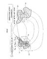
- FIG. 2 is a diagram illustrating a first process of modeling transistor characteristic values with simulation parameters on the basis of circuit characteristic simulation, and a second process of modeling the simulation parameters with the transistor characteristic values;
- FIG. 3 is a diagram illustrating an example of the transistor characteristic
- FIG. 4 is a flowchart of a process of modeling transistor characteristics and the simulation parameters on the basis of the circuit simulation
- FIG. 5A is a flowchart illustrating a process of obtaining a drain current with respect to a drain voltage Vd 1 when a gate voltage is fixed to a predetermined value.
- FIG. 5B is a diagram illustrating a process of extracting a threshold value Vth
- FIG. 6 is an explanatory diagram of an outline of processes of an electronic device manufacturing method
- FIG. 7 is an explanatory diagram illustrating examples of layout pattern information 1 and a net list 2 by use of layout data
- FIG. 8 is a diagram illustrating a bias of a transistor characteristic value obtained from circuit simulation
- FIG. 9 is a flowchart illustrating a process of the computer aided design equipment according to a fourth embodiment
- FIG. 10 is a diagram illustrating a relationship between Vthl and Vths in the case of conducting SPICE-based simulation with simulation parameters by obtaining the simulation parameters in a way that sets the transistor characteristic values scattered equally;
- FIG. 11 is a diagram illustrating an example of a result of obtaining Vthl and Vths by the computer aided design equipment in a first embodiment.
- FIG. 12 is a flowchart illustrating a process of the computer aided design equipment according to a fifth embodiment.
- the technology enables the simulation parameters to be acquired by applying a first mapping relationship when given signal characteristics or characteristic values about circuit components building up a circuit. It is therefore feasible to instruct a simulation unit which simulates the operations of the circuit components with the simulation parameters, to generate the signal characteristics of the circuit constructed by combining the corresponding circuit components by use of the thus-acquired simulation parameters.
- the simulation parameters for simulating the circuit including the circuit components can be obtained.
- FIG. 1 illustrates a block diagram of functions of computer aided design (CAD) equipment.
- the computer aided design equipment is realized as one function of a computer system for designing Large Scale Integration (LSI)
- the computer system assumed herein is realized on a general type of computer.
- the computer includes, e.g., a Central Processing Unit (CPU), a memory, an external storage device, for example, a hard disk, a driving device for a removable portable recording medium, etc., an interface with the external storage device, a communication interface, a display device, and an input/output device, for example, a keyboard, a pointing device such as a mouse, and so on.
- CPU Central Processing Unit
- memory for example, a hard disk, a driving device for a removable portable recording medium, etc.
- an interface with the external storage device e.g., a communication interface, a display device, and an input/output device, for example, a keyboard, a pointing device such as a mouse, and so
- the present computer aided design equipment is realized by a computer program executed by this type of computer.
- the computer program is installed into the hard disk via the communication interface or the driving device for the removable portable recording medium.
- the CPU loads the installed computer program into the memory and then executes the program.
- the functions of the computer aided design equipment are thereby realized.
- the computer provides the functions of the computer aided design equipment, whereby a computer aided design method is carried out.
- the computer aided design equipment includes an input unit/user interface 10 that accepts a user's operation, a simulation instructing unit 11 that starts a process according to an instruction of the input unit/user interface 10 and instructs the simulation unit 12 to execute simulation by setting simulation parameters, a characteristic value extracting unit 13 that extracts a transistor characteristic value from transistor characteristic information generated by the simulation unit 12 , and a simulation parameter determining unit 14 that models the simulation parameter and the transistor characteristic value according to the characteristic value extracted by the characteristic value extracting unit and the simulation parameter.
- the input unit/user interface 10 controls the input device and the display device, and builds up a user interface.
- the input unit/user interface 10 accepts an input from the user, starts up the process, and displays a processing result on the display device.
- the simulation unit 12 is a simulation program such as Simulation Program Integrated Circuits Especially (SPICE).
- SPICE Simulation Program Integrated Circuits Especially
- the term “unit” may be defined as a software module.
- the simulation unit 12 simulates an operation of a circuit assembled by multiple circuit components.
- the circuit operation illustrated by the simulation unit 12 embraces a current/voltage characteristic, delay time and power consumption of each of the circuit components included in the circuit. Further, the circuit operation illustrated by the simulation unit 12 embraces a current/voltage characteristic, delay time and power consumption of the whole circuit.
- a transistor is assumed to be the circuit component.
- the simulation unit 12 accepts a multiplicity of simulation parameters for designating characteristics of the circuit components, and executes the simulation.
- the simulation parameter is defined as a parameter for determining the operation of the circuit component by designating the value of the parameter.
- the simulation unit 12 reproduces the characteristics of the circuit components that are designated by the parameters, and thus simulates the operation of the whole circuit constructed of a combination of these circuit components. Through the simulation, a designer can, if the current/voltage characteristics of the circuit components are already known, confirm the operation of the whole circuit assembled by combining the plural circuit components.
- the simulation instructing unit 11 sets plural combinations of simulation parameters for an individual circuit component, e.g., a transistor.
- the plural combinations of simulation parameters are set within a range defined by designating, e.g., a minimum value and a maximum value at intervals of a predetermined numerical value. Then, the simulation instructing unit 11 instructs the simulation unit 12 to execute the simulation using such combinations of simulation parameters.
- the transistor characteristic information is generated.
- the transistor characteristic information is exemplified such as a current/voltage characteristic expressed by a combination (Vg, Vd, Id) of a gate voltage Vg, a drain voltage Vd and a drain current Id.
- the characteristic value extracting unit 13 selects a characteristic value from the transistor characteristic information and sets the selected value as a transistor characteristic value.
- the transistor characteristic value represents, for example, when the gate voltage Vg is fixed to a predetermined value, a drain current value Id 1 with respect to a drain voltage Vd 1 , a drain current Id 2 with respect to a drain voltage Vd 2 , and so on. Further, the transistor characteristic value represents, when the drain voltage is fixed to a predetermined value, a threshold value Vth obtained as an intersection between an axis of the drain voltage Vd and a tangential line having a maximized micro increment which is a tangential line showing a gradient of the drain current with respect to a micro quantity of variation in the gate voltage.
- the tangential line is abutting the current/voltage characteristics line at the gate voltage.
- the simulation parameter determining unit 14 models a relationship between the combination of the simulation parameters inputted to the simulation unit 12 and the transistor characteristic value obtained as a result of the simulation.
- modeling connotes generating a mapping relationship from one type of value to another.
- the mapping relationship represents a relationship enabling the value to be determined uniquely from one or more variables, and can be exemplified by a polynomial expression of these variables.
- the simulation parameter determining unit 14 has a model generating unit 141 and an inverse mapping determining unit 142 .
- the model generating unit 141 determines the mapping to the transistor characteristic value from the simulation parameter.
- the mapping expresses the transistor characteristic value in the polynomial expression, in which the variables are the simulation parameters, according to a procedure of, e.g., a multiple linear regression analysis.
- the inverse mapping determining unit 142 obtains inverse mapping for inversely transforming the mapping generated by the model generating unit 141 . With this operation, the inverse mapping determining unit 142 expresses the simulation parameters in the polynomial expression, where the variables are the transistor characteristic values.
- the transistor characteristic information is temporarily given in the form of the combination of (Vg, Vd, Id)
- the transistor characteristic value is generated from these values, and the simulation parameter can be immediately acquired.
- a user is enabled to check the operation characteristics of the whole circuit in a way that gives the transistor characteristic information in the form of the combination of (Vg, Vd, Id) to the present computer aided design equipment and executes the simulation of the whole circuit with respect to the circuit including the plurality of transistors having the transistor characteristics thereof.
- the embodiment is not necessarily limited to the process in which the simulation parameter determining unit 14 at first models the transistor characteristic value and thereafter models the simulation parameter by obtaining the inverse mapping. Namely, from the result of the simulation, the simulation parameter may also be directly modeled with the transistor characteristic value. This procedure will be exemplified otherwise by way of a modified example.
- FIGS. 2 through 5 A circuit design method and the computer aided design equipment that supports the circuit design based on this circuit design method according to a first embodiment, will hereinafter be described with reference to the drawings in FIGS. 2 through 5 .
- the computer aided design equipment is given the characteristics of the circuit components building up the circuit, and provides a function of obtaining parameters (the simulation parameters) of a simulation program for simulating the circuit components.
- the simulation parameters are typically a threshold value (Vth 0 ) of a long channel, a saturation velocity (VSAT), a mobility (U 0 ), a gate length (Lg), a gate width (W), dependency of the threshold value upon the drain voltage, a floating body effect, an under-the-gate penetrating diffusion length, etc.
- the simulation parameters may also be parameters into which to express differences from reference values of the parameters such as the threshold value (Vth 0 ) of the long channel, the saturation velocity (VSAT), the mobility (U 0 ), the gate length (Lg), the gate width (W), the dependency of the threshold value upon the drain voltage, the floating body effect and the under-the-gate penetrating diffusion length, or to express quantities of variations thereof by use of a ratio.
- Vth 0 the threshold value of the long channel
- VSAT saturation velocity
- U 0 the mobility
- Lg the gate length
- W the gate width
- dependency of the threshold value upon the drain voltage the floating body effect and the under-the-gate penetrating diffusion length
- deviation quantities from respective standard parameter values in the standard transistors may also be defined. As described above, these parameters are determined for every simulation program.
- the gate length (Lg), the gate width (W), etc are physical quantities corresponding to a gate length and a gate width in a net list. There might be, however, a case in which it is not appropriate to use the design data as it is for the substitution of the simulation parameters even if the simulation parameters correspond to the design data.
- the simulation parameters need setting values that reflect a physical shape formed on the substrate in order to acquire a result of the precise circuit simulation. It is known that especially the gate length (Lg) is easy to be affected by a peripheral layout and exerts great influence on the transistor characteristic, for example, a change in the threshold value due to a short channel effect.
- the simulation unit 12 executes the simulation for every plural gate lengths Lg, and a relationship between the combination of the simulation parameters and the transistor characteristic values acquired as a result of the simulation is modeled per gate length Lg, thereby enabling further improvement to be attained.
- an optimum (a specified gate length Lg) model be selected by referring to the model formula about the layout dependency of the gate length Lg or the table.
- the simulation parameters include the parameter such as the threshold value (Vth 0 ) of the long channel that does not correspond to the design data or the transistor characteristic as the design value.
- the threshold value (Vth 0 ) of the long channel connotes a threshold value when the channel length is sufficiently large, and represents a parameter that can not be set as the transistor characteristic at the gate length of the circuit to be designed in actuality.
- VSAT saturation velocity
- a scheme in the present embodiment is, as described below, to model the relationship between the transistor characteristic values and the simulation parameters.
- FIG. 2 is a diagram illustrating a first process (depicted by [simulation] in FIG. 2 ) of modeling the transistor characteristic values with the simulation parameters on the basis of the circuit characteristic simulation, and illustrating a second process (depicted by [inverse transform] in FIG. 2 ) of modeling the simulation parameters with the transistor characteristic values.
- the second process of modeling the simulation parameters with the transistor characteristic values involves solving inversely the model formula acquired in the first process or alternatively performing the modeling by inverse transform.
- the computer aided design equipment classifies, based on setting given from the user, the multiplicity of simulation parameters into the parameters shown as “modulation parameters” in FIG. 2 in which set values should be changed and into the parameters referred to as “fixed parameters” in which fixed values are set. It is noted that in the following discussion, the modulation parameter is simply termed the simulation parameter.
- the computer aided design equipment executes a circuit characteristic simulation program about multiple combinations of plural simulation parameters.
- the transistor characteristic information is obtained.
- the transistor characteristic information is obtained as a current/voltage characteristic between the source and the drain when, e.g., the gate voltage is fixed. Further, the transistor characteristic information is obtained as a gate voltage/drain current characteristic when the drain voltage is fixed.
- These transistor characteristics are acquired as, for example, the combination of the gate voltage, the drain voltage and the drain current Vgi, Vdi, Idi, where i is an integer.
- the computer aided design equipment extracts a value which will hereinafter be called the transistor characteristic value that characterizes the transistor characteristic information from the acquired transistor characteristic information.
- This value is, e.g., the drain current when the gate voltage Vg and the drain voltage Vd take the predetermined values. Further, this value is, for example, a mutual conductance obtained as a ratio of a quantity of variation in the drain current to a quantity of variation in the gate voltage when the drain voltage is set to the predetermined value in a linear region.
- the computer aided design equipment extracts a plurality of these transistor characteristic values. Then, the computer aided design equipment records a relationship between the combination of the simulation parameters and the combination of the acquired transistor characteristic values. Subsequently, when acquiring the combination of transistor characteristic values with respect to the plural combinations of the simulation parameters, the mapping relationship to the transistor characteristic values from the simulation parameters is obtained. It may be sufficient that the mapping relationship expresses the transistor characteristic values in, e.g., the polynomial expression of the simulation parameters.
- the polynomial expression can be obtained by performing, e.g., the multiple linear regression analysis.
- the multiple linear regression analysis is an analyzing method of fitting a value which is also called a response variable in the polynomial expression to the characteristic value to be acquired in a way that determines a coefficient in the term of independent variables with a plurality of variation quantities being set as the independent variables.
- the term of the polynomial expression is generally equal to or higher than being linear and may contain a product of a plurality of variables. Normally, the coefficient is determined so as to minimize errors between the object characteristic value and the value of the polynomial expression in predetermined domains of the independent variables.
- a simple linear regression analysis an operation of acquiring a formula for predicting one response variable with one independent variable is called a simple linear regression analysis, and this formula can be obtained by a least square method. As broadly known, in the least square method, the coefficient of the formula is determined to minimize a sum of squares of errors between the response variables and actual values.
- the multiple linear regression analysis is what this is extended to the plurality of variables.
- this error is partially differentiated by each coefficient a0, . . . , am, and the minimum value is determined.
- the error is given in the quadratic equation of the coefficient a0, . . . , am, and hence it becomes the linear equation after being partially differentiated. Accordingly, the operation of obtaining the error minimized resolves itself into solving a simultaneous equation.
- a solution of the linear equation on the computer is well known, and hence its explanation is omitted.
- the computer aided design equipment inversely transforms the simulation parameters into the polynomial expression of the transistor characteristic values. This is a process of solving the simultaneous equation organized by the combinations of the plural transistor characteristic values expressed in the polynomial expression of the simulation parameters.
- the computer aided design equipment when the transistor characteristic values are obtained, immediately can acquire the simulation parameters. Accordingly, the simulation of the circuit characteristic can be immediately executed.
- FIG. 3 illustrates an example of the transistor characteristic values. This example illustrates, as the transistor characteristic information, the relationship between the drain voltage Vd and the drain current Id when the gate voltage Vg is fixed and the relationship between the gate voltage Vg and the drain current Id when the drain voltage Vd is fixed.
- the current/voltage characteristic of the single transistor is expressed by a curve. What is actually obtained by the simulation is a combination of discrete values of the gate voltage Vg, the drain voltage Vd and the drain current Id.
- the transistor characteristic value is the value that characterizes the current/voltage characteristic of the single transistor, and is prescribed by a value itself, a gradient, an intercept, a tangential line, etc at a specified point of the current/voltage characteristic.
- the characteristic values used by the computer aided design equipment will hereinafter be exemplified.
- the threshold value of the transistor can be exemplified.
- the threshold value can be, as illustrated in FIG.
- Vth calculated as an intersection Vth between the axis of abscissa (Vg-axis) and a tangential line of Vg 1 at such a point as to maximize a micro increment quantity (the tangential line representing a gradient) of the drain current with respect to a quantity of micro variation of the gate voltage on the gate voltage/drain current characteristic curve when the drain voltage is fixed.
- the calculation of this threshold value corresponds to a predetermined arithmetic operation.
- the drain voltage is set to the power source voltage Vdd
- the gate voltage is the power source voltage Vdd
- at least one of other gate voltages may be set equal to or smaller than 1 ⁇ 2 of a sum of the power source voltage Vdd and the threshold value.
- the gate voltage may be set equal to or smaller than 1 ⁇ 2 of the sum of the power source voltage Vdd and the threshold value.
- the drain current when a predetermined value is set in a body voltage Vbs (which is also referred to as a substrate bias) may also be used.
- Vgs gate voltage
- Vgs gate voltage
- the characteristic values may involve using the mutual conductance (Gmlin) in the linear region, the drain voltage dependency ( ⁇ th) of the threshold value and the floating body effect.
- Vd is set as a predetermined value.
- a change in the mutual conductance may also be used as the floating body effect in place of the threshold value.
- the calculation of the floating body effect corresponds to the predetermined arithmetic operation. It should be noted that the predetermined arithmetic operation is not limited to the above-described calculations of the mutual conductance, ⁇ th, the floating body effect, etc.
- FIG. 4 is a flowchart of a process of modeling the transistor characteristic information and the simulation parameters on the basis of the circuit simulation.
- a type of the characteristic value, which should be extracted from the transistor characteristic information is selected.
- a characteristic value desired by the user is selected as the characteristic value described above. It is preferable that the number of the characteristic values of the transistor be, if possible, same as the number of the changeable simulation parameters. Further, it is also preferable to select such a characteristic value that the transistor characteristic value changes corresponding to a predicted quantity of the physical variation in a way that changes as independently as possible.
- the drain current Idsr 1 changes comparatively independently.
- the mutual conductance in the linear region has a high correlation with the mobility of the electrons.
- the simulation parameters for example, the modulation parameters used in the circuit simulation are selected. These parameters are predetermined for every simulation program.
- the simulation parameters that should be modeled in the way of being associated with the transistor characteristic information for example, the modulation parameters of which the values should be changed are selected from within the multiplicity of parameters. With this selection, it follows that the simulation parameters, which vary with the change in the transistor characteristic information, in other words, the transistor characteristic values, are determined.
- the combination of values, which are set in these simulation parameters are selected.
- the computer aided design equipment determines a maximum variation quantity changeable region defined by the minimum value and the maximum value of each of the selected simulation parameters and also determines an interval at which the simulation is conducted, and selects, based on these determined elements, the combination of the simulation parameters. At this time, round-robin combinations of all the simulation parameters may also be set. Alternatively, an optimum combination as the minimum required according to an orthogonal table may also be set based on an experimental design method which is simply called as experimental design.
- the orthogonal table is an allocation table for an experiment having such a property that all the combinations of the set values of the simulation parameters occur the same number of times with respect to arbitrary two factors which are herein the types of the simulation parameters.
- the experiments are required to be done a number of times corresponding to at least a product of the numbers of combinations of the set values of the simulation parameters. Accordingly, the number of the experiments reaches to a tremendous number if the number of the simulation parameters increases.
- the well-known orthogonal method based on the experimental design enables reduction in the number of the combinations by selecting the parameters having a small dependent relationship.
- the simulation unit 12 executes the circuit simulation per combination (SP 4 ).
- the SPICE-based simulation is carried out.
- the combination of the gate voltage Vg, the drain voltage Vd and the drain current Id (Vgi, Vdi, Idi, where i is the integer) is obtained for the simulation parameter designated by the user.
- the computer aided design equipment extracts the transistor characteristic values selected in SP 1 from the transistor characteristic information acquired by the simulation unit 12 (SP 5 ).
- FIGS. 5A and 5B show examples of the processes of obtaining the transistor characteristic values.
- FIG. 5A is a flowchart showing a process of obtaining the drain current in regard to the drain voltage Vd 1 when the gate voltage is fixed to a predetermined value.
- the computer aided design equipment searches the simulation result for the combination containing the gate voltage that takes a predetermined value Vg 1 .
- a value “V-type(+ ⁇ V)” is simply abbreviated as “V-type” where “-type” is, for example, “d”, “g”, etc.
- the drain current value Id 1 is determined from the obtained combination (Vg 1 , Vd 1 , Id 1 ) (SP 53 ).
- FIG. 5B is the flowchart showing a process of extracting the threshold value Vth.
- the computer aided design equipment generates, based on the procedures described above, a table in which the plurality of transistor characteristic values is associated with the combination of the simulation parameters (SP 6 ).
- the multiple linear regression analysis is conducted based on this table, and the plurality of transistor characteristic values is modeled by the polynomial expression corresponding to a second mapping relationship, where the plural simulation parameters are the variables.
- the threshold value Vth defined as the transistor characteristic value can be expressed by use of four simulation parameters such as Vth 0 , VSAT, U 0 , Lg in the following formula 1.
- the computer aided design equipment executes the procedure of the multiple linear regression analysis, and determines such coefficients a, ai (i is the integer) that the value in the formula 1 fits most to the table value of the characteristic value obtained by the simulation.
- Vth a + a ⁇ ⁇ 0 * Vth ⁇ ⁇ 0 + a ⁇ ⁇ 1 * VSAT + a ⁇ ⁇ 2 * U ⁇ ⁇ 0 + a ⁇ ⁇ 3 * Lg + a ⁇ ⁇ 4 * Vth ⁇ ⁇ 0 * Vth ⁇ ⁇ 0 + a ⁇ ⁇ 5 * VSAT * VSAT + a ⁇ ⁇ 6 * U ⁇ ⁇ 0 * U ⁇ ⁇ 0 + a ⁇ ⁇ 7 * Lg * Lg + a ⁇ ⁇ 8 * Vth ⁇ ⁇ 0 * VSAT + a ⁇ ⁇ 9 * Vth ⁇ ⁇ 0 * U ⁇ ⁇ 0 + a ⁇ ⁇ 10 * Vth ⁇ ⁇ 0 * Lg + a ⁇ ⁇ 11 * VSAT * U ⁇ ⁇ 0 + a ⁇ ⁇ 12 * VSAT * Lg + a ⁇ ⁇ 13 * U ⁇ ⁇ 0 * L
- drain current Ids can be similarly expressed by use of Vth 0 , VSAT, U 0 , Lg in the following formula 2.
- Ids b + b ⁇ ⁇ 0 * Vth ⁇ ⁇ 0 + b ⁇ ⁇ 1 * VSAT + b ⁇ ⁇ 2 * U ⁇ ⁇ 0 + b ⁇ ⁇ 3 * Lg + b ⁇ ⁇ 4 * Vth ⁇ ⁇ 0 * V ⁇ ⁇ th ⁇ ⁇ 0 + b ⁇ ⁇ 5 * VSAT * VSAT + b ⁇ ⁇ 6 * U ⁇ ⁇ 0 * U ⁇ ⁇ 0 + b ⁇ ⁇ 7 * Lg * Lg + b ⁇ ⁇ 8 * Vth ⁇ ⁇ 0 * VSAT + b ⁇ ⁇ 9 * Vth ⁇ ⁇ 0 * U ⁇ ⁇ 0 + b ⁇ ⁇ 10 * Vth ⁇ ⁇ 0 * Lg + b ⁇ ⁇ 11 * VSAT * U ⁇ ⁇ 0 + b ⁇ ⁇ 12 * VSAT * Lg + b ⁇ ⁇ 13 * U ⁇
- Idsr 1 , Idsr 2 , Idst are designated as the transistor characteristics, in which case the values of coefficient of each formula for the characteristic value given above can be similarly obtained.
- next step SP 8 the simulation parameters Vth 0 , VSAT, U 0 , Lg are described in the polynomial expression, in which Ids, Idsr 1 , Idsr 2 , Idst, Vth defined as the transistor characteristic values are the variables.
- the polynomial expression of the simulation parameters obtained in SP 7 is transformed into the polynomial expression of the transistor characteristic values.
- the polynomial expression of the simulation parameters can be transformed into the polynomial expression corresponding to a first mapping relationship of the transistor characteristic values by solving the simultaneous equation.
- the multiple linear regression analysis is performed by using again the table generated in SP 6 , and the respective simulation parameters may be modeled by the polynomial expression of the plurality of transistor characteristic values.
- the transistor characteristic values based on the combination of the simulation parameters may be calculated newly by use of the polynomial expression employed for the modeling in SP 7 .
- the multiple linear regression analysis is carried out by adding the results of these operations, and the simulation parameters may be modeled with the plurality of transistor characteristic values.
- the simulation parameter Vth 0 can be expressed in the following formula 3 by employing the five transistor characteristic values such as Ids, Idsr 1 , Idsr 2 , Idst, Vth.
- Vth ⁇ ⁇ 0 d + d ⁇ ⁇ 0 * Ids + d ⁇ ⁇ 1 * Idsr ⁇ ⁇ 1 + d ⁇ ⁇ 2 * Idsr ⁇ ⁇ 2 + d ⁇ ⁇ 3 * Idst + d ⁇ ⁇ 4 * Vth + d ⁇ ⁇ 5 * Ids * Ids + d ⁇ ⁇ 6 * Idsr ⁇ ⁇ 1 * Idsr ⁇ ⁇ 1 + d ⁇ ⁇ 7 * Idsr ⁇ ⁇ 2 * Idsr ⁇ ⁇ 2 + d ⁇ ⁇ 8 * Idst * Idst + d ⁇ ⁇ 9 * Vth * Vth + d ⁇ ⁇ 10 * Ids * Idsr ⁇ ⁇ 1 + d ⁇ ⁇ 11 * Ids * Idsr ⁇ ⁇ 2 + d ⁇ ⁇ 12 * Ids * Idst + d ⁇
- the mobility U 0 can be expressed similarly to Vth 0 in the following formula 4 by using Ids, Idsr 1 , Idsr 2 , Idst, Vth.
- the procedure of the multiple linear regression analysis remains unchanged.
- the steps described above enable the simulation parameters to be modeled with the transistor characteristic values
- the plurality of transistor characteristic values is modeled by the polynomial expression of the plurality of simulation parameters.
- the relationship between the simulation parameters and the transistor characteristic values can be also expressed by a weighted sigmoid function based on a neurolearning analysis.
- the neurolearning is that plural elements called neurons are combined to organize a mapping relationship to output signals from input signals.
- the output signal is generated by a non-linear function to which each input signal is weight-added.
- the sigmoid function is used as the non-linear function in this case.
- the neurolearning analysis involves connecting, e.g., the combination of the transistor characteristic values to an input of a neural network. Then, the combination of the simulation parameter values is set as a teaching signal.
- the teacher signal connotes a signal that is desirable as the output signal in the neural network. Then, a weight for the weight-addition is determined so as to minimize a squared error between the output signal and the teacher signal in the neural network. A procedure of determining this weight is called the neurolearning.
- a weight coefficient is determined in a direction tracing back to the input side from the output side.
- Japanese Patent Application No. 3110434 proposes an example of the neurolearning and an example of a circuit for realizing the network thereof.
- the neural network when the input signal is organized by the combination of the transistor characteristic values corresponds to the first mapping relationship. Further, the neural network when the input signal is organized by the combination of the simulation parameters corresponds to the second mapping relationship.
- the transistor characteristic values are modeled with the simulation parameters, and, thereafter, the simulation parameters are modeled with the transistor characteristic values by the inverse transform in SP 8 ( FIG. 4 ).
- the simulation parameters may also be immediately modeled with the transistor characteristic values by use of the result of the simulation in SP 6 .
- the mapping relationship acquired at this time corresponds to the first mapping relationship.
- a procedure thereof is the same as SP 7 ( FIG. 4 ).
- a second embodiment will be described with reference to the FIGS. 6 and 7 .
- the first embodiment discussed above has exemplified the computer aided design equipment that acquires, when given the circuit component characteristics such as the transistor characteristic information, the mapping relationship for obtaining the simulation parameters.
- the second embodiment will exemplify the computer aided design equipment that adds, when further given the layout information of the circuit components or the net list, a process of modeling the characteristics from the layout information of the circuit components or from the net list.
- the second embodiment will further exemplify the computer aided design equipment that acquires, if the characteristics of the circuit components, e.g., the layout information or the variables contained in the net list can be described by the polynomial expression, immediately the simulation parameters from the layout information or the net list by applying the polynomial expression and the mapping exemplified in the first embodiment. Still further, the second embodiment will exemplify procedures of executing the simulation based on the simulation parameters, then finally designing the circuit including the electronic components, and thus manufacturing an electronic device.
- the computer aided design equipment that acquires, if the characteristics of the circuit components, e.g., the layout information or the variables contained in the net list can be described by the polynomial expression, immediately the simulation parameters from the layout information or the net list by applying the polynomial expression and the mapping exemplified in the first embodiment. Still further, the second embodiment will exemplify procedures of executing the simulation based on the simulation parameters, then finally designing the circuit including the electronic components, and thus manufacturing
- FIG. 6 is an explanatory diagram illustrating an outline of processes of an electronic device manufacturing method utilizing the computer aided design equipment.
- the computer aided design equipment extracts the transistor characteristic information from layout pattern information 1 of the transistors and a net list 2 (S 1 ).
- the layout pattern information 1 of the transistors contains pieces of information on pattern shapes for defining the individual elements such as the active layer, the gate layer and the contact layer.
- the net list 2 contains mainly circuit connecting information used for connecting the element to the element.
- the net list 2 contains wiring resistance information, capacitance information and design characteristic information.
- the layout pattern information 1 and the net list 2 correspond to the layout information.
- the design characteristic information contains, e.g., a standard gate oxide film thickness, a design gate length, a design gate width, a standard threshold voltage (Vth), a standard mobility, etc which will hereinafter be simply termed standard values.
- the standard gate oxide film thickness, the design gate length, the design gate width, etc are the values that should be said to be target values (design values) at a design stage.
- a semiconductor manufacturing process has a difficulty of forming patterns on a semiconductor substrate as specified by the design values, and there is a case of having discrepancies from the values generated in the actual semiconductor process.
- the terminology involves using an actual gate length and an actual gate width in the sense of dimensional values generated actually on the semiconductor substrate.
- the layout pattern information 1 and the net list 2 are converted into the transistor characteristic values of the transistors that are actually manufactured.
- a relationship between the parameters contained in the layout pattern information 1 and in the net list 2 and the transistor characteristic values based on the manufacturing result is acquired beforehand by modeling.
- This relationship corresponds to a third mapping relationship.
- the modeling is executed offline separately from the design process and the manufacturing process (SQ).
- the modeling process may be done based on the multiple linear regression analysis. Namely, plural combinations of the design characteristic information, e.g., the plural combinations of the standard gate oxide film thickness, a design gate pitch, the design gate length, the design gate width, the standard threshold value, the standard mobility, etc, are generated, and the characteristic information (Ids, Vth, etc) of the transistor manufactured based on these items of design characteristic information is empirically measured. Then, the transistor characteristic values (Ids, Vth, etc) are modeled by the polynomial expression, in which the variables are the elements organizing the combination of the design characteristic information (the transistor characteristic information such as the standard gate oxide film thickness, the design gate pitch, the design gate length, the design gate width, the standard threshold value and the standard mobility).
- the design characteristic information e.g., the plural combinations of the standard gate oxide film thickness, a design gate pitch, the design gate length, the design gate width, the standard threshold value, the standard mobility, etc.
- the simulation parameters are modeled by the polynomial expression of the transistor characteristic values in the procedures explained in the first embodiment (SP).
- the thus-modeled relationship corresponds to the first mapping relationship.
- the polynomial expression of the design characteristic information (the standard gate oxide film thickness, the design gate pitch, the design gate length, the design gate width, the standard threshold value, the standard mobility, etc) obtained in SQ or a calculated value acquired by substituting the design characteristic information into this polynomial expression obtained in SQ, is further substituted into the polynomial expression of the transistor characteristic values obtained in SP.
- the transistor characteristic values obtained in S 1 are substituted into the polynomial expression in S 2 (S 2 ).
- Simulation parameters 4 are thereby obtained from the design characteristic information.
- a relationship with which the simulation parameters 4 are obtained from the design characteristic information corresponds to a fourth mapping relationship.
- the computer aided design equipment executes the circuit characteristic simulation by use of the simulation parameters 4 (S 3 ).
- the circuit characteristic simulation enables the acquisition of the characteristics of the circuit constructed by connecting the plurality of circuit components of the transistor etc.
- the characteristics of the circuit represent, e.g., power consumption, a delay time, etc of the circuit.
- the computer aided design equipment determines whether the circuit characteristics reach the target criteria or not (S 4 ). Subsequently, if unable to attain the target standard values, the computer aided design equipment prompts the user to change the layout pattern information 1 or the net list 2 . The user changes, based on a change-prompting message, the layout pattern information 1 or the net list 2 (S 5 ).
- the design gate width of any one of the transistors is expanded in order to attain high-speed driving.
- the design gate length may be reduced.
- the design gate width is reduced. Then, in response to an instruction given from the user, the computer aided design equipment repeats the processes in S 1 through S 4 .
- the computer aided design equipment further advances the layout computer aided design.
- pieces of layout data of each of the layers for manufacturing a reticle are generated.
- the semiconductor manufacturing process is executed, and the electronic device is manufactured (S 6 ).
- the semiconductor manufacturing process includes the film formation, oxidation, the photolithography, developing, etching, implantation of an impurity, a thermal treatment, etc. This type of manufacturing process enables the semiconductor circuit having the target circuit characteristics to be manufactured.
- the transistor characteristic values are modeled by the parameters contained in the layout pattern information 1 and in the net list 2 , the transistor characteristic values expressed by the model formula thereof are substituted into the polynomial expression for extracting the simulation parameters which will hereinafter be also referred to as an extraction formula described in the first embodiment, whereby the data in the layout pattern information 1 and in the net list 2 can be converted into the simulation parameters. Then, it is feasible to predict with high accuracy the circuit characteristics such as the delay time of the circuit including the plurality of transistors depending on the layout.
- the transistor characteristic values are expressed as below.
- the threshold voltage Vth and the drain current Ids are modeled by the polynomial expression of a gate pitch p, the gate length Lg, a source/drain width SB for example, a width of the source region, or a width of the drain region, a source/drain Shallow Trench Isolation (STI) offset SBOF, for example, an offset distance from the region of the element isolation film in the source region, or an offset distance from the region of the element isolation film in the drain region, etc of the transistor, and are then described in the following formulae 5 and 6.
- STI Shallow Trench Isolation
- Vth c + c ⁇ ⁇ 0 * p + c ⁇ ⁇ 1 * Lg + c ⁇ ⁇ 2 * W + c ⁇ ⁇ 3 * SB + c ⁇ ⁇ 4 * SA + c ⁇ ⁇ 5 * SBOF + c ⁇ ⁇ 6 * p * Lg + c ⁇ ⁇ 7 * p * W + c ⁇ ⁇ 8 * p * SB + c ⁇ ⁇ 9 * p * SA + c ⁇ ⁇ 10 * p * SBOF + c ⁇ ⁇ 11 * Lg * W + c ⁇ ⁇ 12 * Lg * SB + c ⁇ ⁇ 13 * Lg * SA + c ⁇ ⁇ 14 * Lg * SBOF + c ⁇ ⁇ 15 * W * SB + c ⁇ ⁇ 16 * W * SA + c ⁇ ⁇ 17 * W * SBOF + c ⁇ ⁇ 18 * SB * SA + c ⁇ ⁇ 19 * SB * SBO
- the characteristics of the transistor manufactured based on the layout pattern information 1 and the net list 2 shown in FIG. 7 may be actually measured in accordance with the procedures explained in FIG. 6 .
- the threshold voltage Vth, the drain current Ids, etc of the transistor may be actually measured.
- a relationship between the threshold voltage Vth, the drain current Ids, etc and the combination of the parameters in the net list 2 is subjected to the multiple linear regression analysis, and the coefficient of the polynomial expression as in the formulae 5 and 6 may be determined.
- these formulae when the transistor characteristic values are modeled by the polynomial expression of the parameters contained in the layout pattern information 1 or the net list 2 , these formulae may be substituted directly into the polynomial expressions of the transistor characteristic values such as the formulae 3, 4, etc. With this operation, it is possible to acquire the mapping to the simulation parameters from the parameters contained in the layout pattern information 1 or the net list 2 .
- the simulation parameters can be immediately obtained. It is therefore feasible to check the operation of the circuit including the plurality of circuit components defined by the layout pattern information 1 or the net list 2 . Then, if the circuit operation satisfies the predetermined criteria, the design further proceeds, and it is possible to manufacture the reticle and the electronic device based on the semiconductor manufacturing process.
- the process-dependent transistor characteristics can be converted into the simulation parameters by substituting the transistor characteristic values expressed in the model formula into the simulation parameter extraction formula described in the first embodiment.
- a mapping relationship for converting the combination of the process parameters into the transistor characteristic values corresponds to a fifth mapping relationship.
- a mapping relationship for converting the combination of the process parameters into the simulation parameters corresponds to a sixth mapping relationship.
- Vth f + f ⁇ ⁇ 0 * DOSE ⁇ ( a ) + f ⁇ ⁇ 1 * ENERGY ⁇ ( a ) + f ⁇ ⁇ 2 * DOSE ⁇ ( b ) + f ⁇ ⁇ 3 * ENERGY ⁇ ( b ) + f ⁇ ⁇ 4 * DOSE ⁇ ( a ) * ENERGY ⁇ ( a ) + f ⁇ ⁇ 5 * DOSE ⁇ ( a ) * DOSE ⁇ ( b ) + f ⁇ ⁇ 6 * DOSE ⁇ ( a ) * ENERGY ⁇ ( b ) + f ⁇ ⁇ 7 * ENERGY ⁇ ( a ) * DOSE ⁇ ( b ) + f ⁇ ⁇ 8 * ENERGY ⁇ ( a ) * ENERGY ⁇ ( b ) + f ⁇ ⁇ 9 * DOSE ⁇ ( b ) * ENERGY
- the transistor characteristic values depending on the layout pattern information 1 and the net list 2 are fixed. Namely, herein, the layout pattern information 1 and the net list 2 is kept in the fixed status, and then the analysis in the case where the process change is made is executed.
- the first embodiment has exemplified the computer aided design equipment that models the simulation parameters with the transistor characteristic values directly from the simulation result. Further, the second embodiment has exemplified the computer aided design equipment that acquires the simulation parameters from the layout information of the circuit components or from the net list. Still further, the third embodiment has exemplified the computer aided design equipment that converts the process-dependent transistor characteristics into the simulation parameters.
- the fourth embodiment will exemplify the computer aided design equipment that obtains such simulation parameters with much higher accuracy.
- Other configurations and operations are the same as those in the first through third embodiments. This being the case, the components, which are the same as those in the first through the third embodiments, are marked with the same symbols and numerals, and their explanations are omitted. Further, the drawings in FIGS. 1 through 7 will be referred to when the necessity arises.
- the simulation parameter extracting method is illustrated by which the simulation parameters are modeled with the transistor characteristic values on the basis of the circuit simulation. This method might, however, cause a case of relatively lacking in the precision for the following reasons.
- FIG. 8 shows a bias in the transistor characteristic value acquired from the circuit simulation.
- FIG. 8 illustrates a relationship between the transistor characteristic values obtained by the simulation using the combination of the plural simulation parameters based on the experimental design and the simulation parameters at this time.
- the data has no bias because of being based on the experimental design (a grid G 1 on the right side conceptually represents the combination of the simulation parameters selected when executing the simulation).
- the bias might, however, occur in the combination of the transistor characteristics acquired from the simulation.
- the reason for this occurrence is that the simulation parameter and the transistor characteristic value do not necessarily have a relationship of the linear function.
- a concept of the data (a transistor characteristic distribution) in which curved surfaces are acquired by the simulation is illustrated on the left side in FIG. 8 .
- a hypothesis is that on the left side in FIG. 8 , a thick mesh area (a symbol A 2 ) has a great number of samples of the data, a thin mesh area (a symbol A 1 ) has a small number of samples of the data, and a peripheral area has none of the data.
- the target transistor characteristic values are not attained.
- the area A 1 depicted by ⁇ has the small data count and therefore has a large regression error. This is because the multiple linear regression analysis involves determining the polynomial expression so as to fit most to, generally, the data to be modeled, and hence it is impossible to acquire, if the data itself to be modeled has a small data count, the model based on the highly accurate analyzed result, i.e., the highly accurate polynomial expression.
- the fourth embodiment provides a technology of converting changes caused by the differences of the layout data of the transistor characteristics, the pattern layout and the manufacturing process into the parameters used in the circuit simulation with the high accuracy.
- FIG. 9 is a flowchart showing processes of the computer aided design equipment according to the fourth embodiment.
- the processes in SP 1 -SP 6 are the same as those in FIG. 4 , which have been explained in the cases of the first through third embodiments.
- the multiple linear regression analysis is carried out based on the table generated in the process in SP 6 , and the plurality of simulation parameters is modeled by the polynomial expression of the plurality of transistor characteristic values (SP 8 A).
- the transistor characteristic values are temporarily modeled as the polynomial expression of the simulation parameters and may be inversely transformed.
- the simulation parameters may be modeled by the polynomial expression of the transistor characteristic values.
- the computer aided design equipment predicts beforehand a fluctuation range of the actual transistor characteristics, then determines a range of the maximum value through the minimum value of the characteristic values and the number of levels thereof, and further determines, based on the determined elements, the combination of the plural transistor characteristic values (SP 9 ).
- the transistor characteristic values may be equally allocated within the range of the maximum value through the minimum value.
- the phrase “equally allocated” connotes “obtaining points for dividing the range of the maximum value through the minimum value at equal intervals or intervals approximate to the equal intervals”.
- the CPU of the computer aided design equipment, which executes the process in SP 9 corresponds to a characteristic value setting unit.
- a further available process is a process of constraining the conditions so as not to cause any contradiction in a magnitude relationship between the determined combinations of the transistor characteristic values.
- a threshold value (Vthl) in the linear region of the transistor characteristics is always larger than a threshold value (Vths) in the saturation region. Therefore, a difference (dVthl) of the threshold value (Vthl) in the linear region from the threshold value (Vths) in the saturation region is defined, and the combination with no contradiction can be determined by calculating the threshold value (Vthl) in the linear region in a way that uses a combination of the threshold value (Vths) in the saturation region and the difference (dVthl, a non-negative value).
- the mutual conductance (Gmlin) in the linear region of the transistor characteristics invariably takes a value smaller than the mutual conductance (Gmsat) in the saturation region.
- a ratio ( ⁇ Gmlin, “1” or larger) of the mutual conductance (Gmsat) in the saturation region to the mutual conductance (Gmlin) in the linear region is defined, and the mutual conductance (Gmsat) in the saturation region is calculated by use of a combination of the mutual conductance (Gmlin) in the linear region and the ratio ( ⁇ Gmlin), thereby enabling the combination with no contradiction to be determined.
- a plurality of current values in the predetermined voltage or a plurality of voltage values in the predetermined current can be used as the transistor characteristics.
- the simulation parameters are predicted based on the model generated in SP 8 A (SP 10 ). Specifically, the combination of the transistor characteristic values acquired in SP 9 is substituted into the polynomial expression of the transistor characteristic values acquired in SP 8 , thereby obtaining the values of the simulation parameters (the combination of the simulation parameters, corresponding to the combination of the transistor characteristic values) (SP 10 ).
- the CPU of the computer aided design equipment, which executes the process in SP 10 corresponds to a simulation parameter acquiring unit.
- the then-predicted combination of the simulation parameters takes, conceptually, for example, as illustrated in an area A 3 on the right side in FIG. 8 , a shape that is more distorted than the initially-set combination (the grid G 1 ) of the simulation parameters.
- the computer aided design equipment again executes the process in SP 4 on the basis of the combination of the simulation parameters, which is predicted in SP 10 .
- the CPU of the computer aided design equipment which executes a loop of processing from SP 10 back to SP 4 , corresponds to a control unit. Namely, the CPU executes the circuit simulation for every combination of the simulation parameters acquired in SP 10 . This operation enables generation of a table containing the transistor characteristic values in which the bias in the transistor characteristic is reduced. The accuracy of the table generated in SP 8 A can be enhanced by repeating this loop of processing once or more.
- FIG. 10 illustrates a relationship between Vthl and Vths in the case of obtaining the simulation parameters in the way of equally setting the transistor characteristic values and conducting the SPICE-based simulation by use of these simulation parameters.
- FIG. 10 shows a result of obtaining Vthl and Vths defined as the transistor parameters by executing once the control of looping the processing from SP 9 back to SP 4 in FIG. 9 .
- the simulation parameters become a distorted aggregation of the values as in the area A 3 in FIG. 8 .
- FIG. 11 shows an example of a result of obtaining Vthl and Vths by the computer aided design equipment according to the first embodiment.
- Vthl and Vths are acquired by equally setting the simulation parameters.
- Vthl and Vths take the correlation, however, for example, in the case of changing the impurity in the channel region, there might be a case where the correlation between Vthl and Vths gets collapsed. According to the procedures in the first embodiment, there might also be a case in which the setting of the multiple simulation parameters including such a case is not necessarily sufficient. On the other hand, adoption of the procedures in the fourth embodiment illustrates that the multiple simulation parameters having none of such a correlation can be set.
- the computer aided design equipment in the fourth embodiment obtains the transistor characteristic values SP 1 -SP 5 in FIG. 9 from the result of the simulation with respect to the combination of the simulation parameters in the same way as in the first through third embodiments.
- the combinations of the values may be selected as the simulation parameters at the equal intervals.
- the simulation parameters are modeled by the polynomial expression in which the variables are the transistor characteristic values.
- the result with the bias is obtained as the transistor characteristic values by the simulation in SP 4 in FIG. 9 in many cases. Accordingly, in the area with the small quantity of data, there might occur such a case that the simulation parameters can not be modeled with the transistor characteristic values with the high accuracy, depending on the multiple linear regression analysis.
- the combination of the transistor characteristic values is equally selected and substituted into the polynomial expression of the transistor characteristic values, thereby predicting the simulation parameters.
- the result of this prediction does not show, in many cases, the uniformity in a space of the simulation parameters (see an area A 3 in FIG. 8 ).
- the simulation is again executed by use of the predicted simulation parameters, whereby it is possible to acquire the transistor characteristic values with the less bias than in the case of executing the simulation by using the equally allocated simulation parameters.
- the transistor characteristic values with a much smaller bias can be acquired by repeating the processes in SP 9 -SP 4 in FIG. 9 plural number of times.
- the simulation parameters can be modeled with the transistor characteristic values with the even higher accuracy than by the processes of the computer aided design equipment without the loop of processing from SP 9 back to SP 4 in FIG. 9 .
- the computer aided design equipment is capable of converting the changes caused by the differences of the layout data of the transistor characteristics, the pattern layout and the manufacturing process into the parameters used in the circuit simulation with the high accuracy, and also capable of highly precisely predicting the circuit characteristics such as the delay time of the circuit including the plurality of layout dependent transistors. Further, the computer aided design equipment can predict the circuit characteristics such as the delay time due to the slight change in the process with the high accuracy.
- the fourth embodiment has exemplified the computer aided design equipment that obtains again the simulation parameters by temporarily substituting the equally-distributed transistor characteristic values into the simulation parameters modeled with the transistor characteristic values, and repeats again the circuit simulation.
- the fourth embodiment has exemplified the computer aided design equipment that executes, as shown in FIG. 9 , the loop of the processes of modeling the simulation parameters with the transistor characteristic values (SP 8 A), selecting the combination of the transistor characteristic values (SP 9 ), predicting the simulation parameters (SP 10 ) and executing the simulation (SP 4 ).
- a fifth embodiment will exemplify the computer aided design equipment that executes a process, in the processes according to the fourth embodiment, of repeating the processing loop described above and narrowing the transistor characteristic values down to a predetermined value.
- Other configurations and operations are the same as those in the fourth embodiment. This being the case, the components, which are the same as those in the fourth embodiment, are marked with the same symbols and numerals, and their explanations are omitted.
- FIG. 12 is a flowchart showing a process of the computer aided design equipment according to the fifth embodiment.
- the steps other than SP 9 A are the same as those in FIG. 9 .
- the computer aided design equipment is given a central value and a range of a predetermined deviation from the central value as the transistor characteristic values and sets the combination of the transistor characteristic values.
- the threshold value Vthl in the linear region there is set a combination of five values such as Vthl 0 ⁇ Vthl, Vthl 0 ⁇ Vthl/2, Vthl 0 , Vthl 0 + ⁇ Vthl/2 and Vthl 0 + ⁇ Vthl.
- ⁇ Vthl is the deviation to be prescribed from the central value with respect to the threshold value Vthl in the linear region.
- ⁇ Vths is the deviation to be prescribed from the central value with respect to the threshold value Vths in the saturation region.
- ⁇ gml is the deviation to be prescribed from the central value with respect to the mutual conductance Gmlin in the linear region.
- ⁇ gms is the deviation to be prescribed from the central value with respect to the mutual conductance Gmsat in the saturation region.
- a combination of the values which should be substituted into the combination of the variables (Vthl, Vths, Gmlin, Gmsat) of the transistor characteristic values, is generated by combining these values.
- the case of the fourth embodiment is similarly applied to the point of establishing the conditions such as Vthl>Vths and Gmsat>Gmlin. It should be noted that the number of these values is not limited to “5”.
- an average value, a mode or the central value, etc, which are obtained from the semiconductor manufacturing process in the present design data may be set as the central value of the transistor characteristic values.
- a fluctuations acquired in the step may be set as the predetermined deviation from the central value.
- the semiconductor manufacturing process and the central value of the simulation parameters corresponding to the semiconductor manufacturing process are not frequently changed, and hence the simulation targeted at the specified semiconductor manufacturing process or the specified design data can be attained.
- the predetermined deviation ⁇ from the central value is fixed. In place of these procedures, however, any inconvenience may not be caused by setting the deviation ⁇ so as to be decreased stepwise per loop of the processing.
- the deviation ⁇ is set to a value (e.g., 2-fold value, a 10-fold value or a 100-fold value) larger than the manufacturing fluctuations in the specified semiconductor manufacturing process, and may be then set small (changed to a 1 ⁇ 2-fold value, a 1/10-fold value or 1/100-fold value) per loop of the processing.
- the deviation ⁇ is set large for the first time and then decreased each time the operation loops the steps round, whereby the relationship between the central value of the simulation parameters and the central value of the transistor characteristic values can be precisely acquired, Namely, at the initial stage, the modeling is executed in the comparatively wide parameter range, and the range of the transistor characteristic values is narrowed down stepwise, thereby making it feasible to reduce a possibility of converging on a singular model.
- a program for making a computer, other machines and devices which will hereinafter be referred to as the computer etc, realize any one of the functions can be recorded on a recording medium readable by the computer etc. Then, the computer etc is made to read and execute the program on this recording medium, whereby the function thereof can be provided.
- the recording medium readable by the computer etc connotes a recording medium capable of storing information such as data and programs electrically, magnetically, optically, mechanically or by chemical action, which can be read from the computer etc.
- these recording mediums for example, a flexible disc, a magneto-optic disc, a CD-ROM, a CD-R/W, a DVD, a DAT, an 8 mm tape, a memory card, etc are given as those removable from the computer.
- a hard disc a Read-Only Memory (ROM), etc are given as the recording mediums fixed within the computer etc.
Abstract
Description
where DOSE(a) is a channel impurity implantation quantity, ENERGY(a) is a channel impurity implantation energy, DOSE(b) is a halo (pocket) impurity implantation quantity, and ENERGY(b) is a halo (pocket) impurity implantation energy. Herein, the term “pocket” connotes an impurity region that forms part of the channel into which the impurity is implanted with a gate and a sidewall serving as a mask.
Vth1=Vths+dVthl,
where dVthl>=0;
Gmsat=αGmlin*Gmlin,
where αGmlin>=1.
Namely, the combination of the characteristic values may be calculated such as (Vths+dVthl, Vths, Gmlin, αGmlin*Gmlin). Then, the value may be selected within the range of dVthl>=0. Moreover, the value may also be selected within the range of αGmlin>=1.
Claims (23)
Applications Claiming Priority (4)
| Application Number | Priority Date | Filing Date | Title |
|---|---|---|---|
| JP2007-054787 | 2007-03-05 | ||
| JP2007054787 | 2007-03-05 | ||
| JP2007274149A JP5167756B2 (en) | 2007-03-05 | 2007-10-22 | Design support apparatus, design support program, design support method, and semiconductor circuit manufacturing method |
| JP2007-274149 | 2007-10-22 |
Publications (2)
| Publication Number | Publication Date |
|---|---|
| US20080221854A1 US20080221854A1 (en) | 2008-09-11 |
| US8935146B2 true US8935146B2 (en) | 2015-01-13 |
Family
ID=39742525
Family Applications (1)
| Application Number | Title | Priority Date | Filing Date |
|---|---|---|---|
| US12/042,059 Expired - Fee Related US8935146B2 (en) | 2007-03-05 | 2008-03-04 | Computer aided design apparatus, computer aided design program, computer aided design method for a semiconductor device and method of manufacturing a semiconductor circuit based on characteristic value and simulation parameter |
Country Status (1)
| Country | Link |
|---|---|
| US (1) | US8935146B2 (en) |
Cited By (1)
| Publication number | Priority date | Publication date | Assignee | Title |
|---|---|---|---|---|
| US10140415B2 (en) | 2016-03-04 | 2018-11-27 | Samsung Electronics Co., Ltd. | Method and system for verifying layout of integrated circuit including vertical memory cells |
Families Citing this family (9)
| Publication number | Priority date | Publication date | Assignee | Title |
|---|---|---|---|---|
| US7979815B2 (en) * | 2008-01-08 | 2011-07-12 | International Business Machines Corporation | Compact model methodology for PC landing pad lithographic rounding impact on device performance |
| US8103990B2 (en) * | 2008-02-28 | 2012-01-24 | Arm Limited | Characterising circuit cell performance variability in response to perturbations in manufacturing process parameters |
| US20100125441A1 (en) * | 2008-11-17 | 2010-05-20 | Vns Portfolio Llc | Method and Apparatus for Circuit Simulation |
| US8793642B2 (en) * | 2009-12-23 | 2014-07-29 | Biosense Webster (Israel), Ltd | Component selection for circuit assembly |
| JP2011222835A (en) | 2010-04-12 | 2011-11-04 | Fujitsu Semiconductor Ltd | Integrated circuit manufacturing/designing method and program |
| US9563729B2 (en) | 2013-06-21 | 2017-02-07 | Cryptography Research, Inc. | Signal transition analysis of a circuit |
| CN109791627B (en) * | 2018-06-19 | 2022-10-21 | 香港应用科技研究院有限公司 | Semiconductor device modeling for training deep neural networks using input preprocessing and conversion targets |
| CN114902337A (en) * | 2019-12-31 | 2022-08-12 | 美光科技公司 | Mobile storage random read performance estimation enhancement |
| CN111400867B (en) * | 2020-02-18 | 2023-05-02 | 西安电子科技大学 | Simulation analysis-based microwave solid-state emission reliability design method |
Citations (53)
| Publication number | Priority date | Publication date | Assignee | Title |
|---|---|---|---|---|
| US5313398A (en) * | 1992-07-23 | 1994-05-17 | Carnegie Mellon University | Method and apparatus for simulating a microelectronic circuit |
| US5553008A (en) * | 1993-03-29 | 1996-09-03 | Epic Design Technology Inc. | Transistor-level timing and simulator and power analyzer |
| US5757679A (en) * | 1995-08-01 | 1998-05-26 | Matsushita Electric Industrial Co., Ltd. | Method and apparatus for modelling MOS transistor characteristics for semiconductor circuit characteristic analysis |
| US5764532A (en) * | 1995-07-05 | 1998-06-09 | International Business Machines Corporation | Automated method and system for designing an optimized integrated circuit |
| US6031246A (en) * | 1994-03-17 | 2000-02-29 | Fujitsu Limited | Method of producing semiconductor devices and method of evaluating the same |
| JP2000293566A (en) | 1999-04-09 | 2000-10-20 | Nec Ic Microcomput Syst Ltd | Method for extracting model parameter |
| US6219630B1 (en) * | 1995-12-07 | 2001-04-17 | Matsushita Electronics Corporation | Apparatus and method for extracting circuit, system and method for generating information for simulation, and netlist |
| US6330526B1 (en) * | 1998-09-30 | 2001-12-11 | Mitsubishi Denki Kabushiki Kaisha | Characteristic variation evaluation method of semiconductor device |
| US20020010565A1 (en) * | 1999-12-28 | 2002-01-24 | Shirun Ho | Method to support the setup of input parameters |
| US20020008252A1 (en) * | 2000-06-27 | 2002-01-24 | Matsushita Electric Industrial Co., Ltd | Method of estimating lifetime of semiconductor device, and method of reliability simulation |
| US6425111B1 (en) * | 1999-12-30 | 2002-07-23 | The Board Of Trustees Of The Leland Stanford Junior University | Saturation region transistor modeling for geometric programming |
| US20020156609A1 (en) * | 2001-04-19 | 2002-10-24 | Matsushita Electric Industrial Co., Ltd. | Circuit simulation method, circuit simulation device, and circuit simulation program and computer readable storage medium onto which the program is stored |
| US20030117163A1 (en) * | 2001-12-25 | 2003-06-26 | Mitsubishi Denki Kabushiki Kaisha | Testing apparatus and method of measuring operation timing of semiconductor device |
| US6618837B1 (en) * | 2000-09-14 | 2003-09-09 | Cadence Design Systems, Inc. | MOSFET modeling for IC design accurate for high frequencies |
| US6698000B2 (en) * | 2001-04-16 | 2004-02-24 | Mitsubishi Denki Kabushiki Kaisha | Semiconductor process parameter determining method, semiconductor process parameter determining system, and semiconductor process parameter determining program |
| US20040044511A1 (en) * | 2002-08-27 | 2004-03-04 | Matsushita Electric Industrial Co., Ltd | Circuit simulation method |
| US20040064296A1 (en) * | 2000-10-17 | 2004-04-01 | Sharad Saxena | Method for optimizing the characteristics of integrated circuits components from circuit specifications |
| US6735558B1 (en) * | 1999-07-19 | 2004-05-11 | Renesas Technology Corp. | Characteristic extraction device, characteristic evaluation device, characteristic extraction method, characteristic evaluation method, recording medium and semiconductor device |
| US6861849B2 (en) * | 2002-07-09 | 2005-03-01 | Oki Electric Industry Co., Ltd. | Capacity measuring device and capacity measuring method |
| US20050086033A1 (en) * | 2002-08-30 | 2005-04-21 | Cadence Design Systems, Inc. | Extracting semiconductor device model parameters |
| US20050138581A1 (en) * | 2002-12-19 | 2005-06-23 | Hiroki Usui | Semiconductor circuit device simulation method and semiconductor circuit device simulator |
| US20050172251A1 (en) * | 2003-11-06 | 2005-08-04 | Li-Fu Chang | Delta-geometry timing prediction in integrated circuit fabrication |
| US20050278677A1 (en) * | 2004-06-10 | 2005-12-15 | Chartered Semiconductor Manufacturing Ltd. | Novel test structure for automatic dynamic negative-bias temperature instability testing |
| US20050288918A1 (en) * | 2004-06-24 | 2005-12-29 | Chen Thomas W | System and method to facilitate simulation |
| US20060142987A1 (en) * | 2004-12-24 | 2006-06-29 | Matsushita Electric Industrial Co., Ltd. | Circuit simulation method and circuit simulation apparatus |
| US20060150132A1 (en) * | 2004-12-31 | 2006-07-06 | Blaze-Dfm, Inc. | Method and system for finding an equivalent circuit representation for one or more elements in an integrated circuit |
| US20060173667A1 (en) * | 2005-01-31 | 2006-08-03 | Takashi Sumikawa | Simulation device for integrated circuit |
| US20060224255A1 (en) * | 2003-08-21 | 2006-10-05 | Masato Tanaka | Pid parameter adjustment device |
| JP2006329824A (en) | 2005-05-26 | 2006-12-07 | Matsushita Electric Ind Co Ltd | Circuit simulation method |
| US20060282249A1 (en) * | 2005-06-09 | 2006-12-14 | Matsushita Electric Industrial Co., Ltd. | Circuit simulation method and circuit simulation apparatus |
| US7155685B2 (en) * | 2002-12-27 | 2006-12-26 | Sipec Corporation | Optimizing designing apparatus of integrated circuit, optimizing designing method of integrated circuit, and storing medium in which program for carrying out optimizing designing method of integrated circuit is stored |
| US7197728B2 (en) * | 2003-06-17 | 2007-03-27 | Matsushita Electric Industrial Co., Ltd. | Method for setting design margin for LSI |
| US20070106966A1 (en) * | 2005-11-08 | 2007-05-10 | Fujitsu Limited | Method and apparatus for extracting characteristic of semiconductor integrated circuit |
| US7268575B1 (en) * | 2006-04-06 | 2007-09-11 | Taiwan Semiconductor Manufacturing Co., Ltd. | Method of NBTI prediction |
| US7315992B2 (en) * | 2004-07-29 | 2008-01-01 | Texas Instruments Incorporated | Electro-migration (EM) and voltage (IR) drop analysis of integrated circuit (IC) designs |
| US7320116B2 (en) * | 2005-03-25 | 2008-01-15 | Fujitsu Limited | Method of generating cell library data for large scale integrated circuits |
| US20080028342A1 (en) * | 2006-07-25 | 2008-01-31 | Hiroshi Tsuji | Simulation apparatus and simulation method used to design characteristics and circuits of semiconductor device, and semiconductor device fabrication method |
| US20080109767A1 (en) * | 2006-11-06 | 2008-05-08 | Fujitsu Limited | Layout method of semiconductor circuit, program and design support system |
| US20080195983A1 (en) * | 2007-02-12 | 2008-08-14 | International Business Machines Corporation | Semiconductor device stress modeling methodology |
| US7462914B2 (en) * | 2005-07-21 | 2008-12-09 | Panasonic Corporation | Semiconductor circuit device and simulation method of the same |
| US20090089037A1 (en) * | 2007-10-01 | 2009-04-02 | Nec Electronics Corporation | Method and apparatus for circuit simulation in view of stress exerted on MOS transistor |
| US7533359B2 (en) * | 2005-05-20 | 2009-05-12 | Cadence Design Systems, Inc. | Method and system for chip design using physically appropriate component models and extraction |
| US20090172611A1 (en) * | 2007-12-26 | 2009-07-02 | Fujitsu Microelectronics Limited | Method for manufacturing semiconductor device |
| US20090249263A1 (en) * | 2008-03-28 | 2009-10-01 | Fujitsu Microelectronics Limited | Semiconductor circuit design method and semiconductor circuit manufacturing method |
| US7617056B2 (en) * | 2005-12-27 | 2009-11-10 | Semiconductor Energy Laboratory Co., Ltd. | Parameter extraction method, method for inspecting circuit operation, and storage medium having program to perform the parameter extraction method |
| US20090306953A1 (en) * | 2008-06-06 | 2009-12-10 | Synopsys, Inc. | Generating Variation-Aware Library Data With Efficient Device Mismatch Characterization |
| US7913214B2 (en) * | 2007-07-17 | 2011-03-22 | Renesas Electronics Corporation | Method and program for designing semiconductor integrated circuit |
| US20110093245A1 (en) * | 2009-10-16 | 2011-04-21 | Fujitsu Semiconductor Limited | Model generating computer product, apparatus, and method |
| US20110237005A1 (en) * | 2010-03-23 | 2011-09-29 | Daewook Kim | Layout Testing Method and Wafer Manufacturing Method |
| US8271254B2 (en) * | 2006-07-28 | 2012-09-18 | Panasonic Corporation | Simulation model of BT instability of transistor |
| US8484597B2 (en) * | 2010-04-12 | 2013-07-09 | Fujitsu Semiconductor Limited | Integrated circuit manufacturing method, design method and program |
| US8498855B2 (en) * | 2008-09-26 | 2013-07-30 | Renesas Electronics Corporation | Circuit simulation based on gate spacing from adjacent MOS transistors |
| US8555224B2 (en) * | 2010-12-13 | 2013-10-08 | Panasonic Corporation | Circuit simulation method and semiconductor integrated circuit |
-
2008
- 2008-03-04 US US12/042,059 patent/US8935146B2/en not_active Expired - Fee Related
Patent Citations (60)
| Publication number | Priority date | Publication date | Assignee | Title |
|---|---|---|---|---|
| US5313398A (en) * | 1992-07-23 | 1994-05-17 | Carnegie Mellon University | Method and apparatus for simulating a microelectronic circuit |
| US5553008A (en) * | 1993-03-29 | 1996-09-03 | Epic Design Technology Inc. | Transistor-level timing and simulator and power analyzer |
| US6031246A (en) * | 1994-03-17 | 2000-02-29 | Fujitsu Limited | Method of producing semiconductor devices and method of evaluating the same |
| US5764532A (en) * | 1995-07-05 | 1998-06-09 | International Business Machines Corporation | Automated method and system for designing an optimized integrated circuit |
| US5757679A (en) * | 1995-08-01 | 1998-05-26 | Matsushita Electric Industrial Co., Ltd. | Method and apparatus for modelling MOS transistor characteristics for semiconductor circuit characteristic analysis |
| US6219630B1 (en) * | 1995-12-07 | 2001-04-17 | Matsushita Electronics Corporation | Apparatus and method for extracting circuit, system and method for generating information for simulation, and netlist |
| US6330526B1 (en) * | 1998-09-30 | 2001-12-11 | Mitsubishi Denki Kabushiki Kaisha | Characteristic variation evaluation method of semiconductor device |
| JP2000293566A (en) | 1999-04-09 | 2000-10-20 | Nec Ic Microcomput Syst Ltd | Method for extracting model parameter |
| US6735558B1 (en) * | 1999-07-19 | 2004-05-11 | Renesas Technology Corp. | Characteristic extraction device, characteristic evaluation device, characteristic extraction method, characteristic evaluation method, recording medium and semiconductor device |
| US20020010565A1 (en) * | 1999-12-28 | 2002-01-24 | Shirun Ho | Method to support the setup of input parameters |
| US6425111B1 (en) * | 1999-12-30 | 2002-07-23 | The Board Of Trustees Of The Leland Stanford Junior University | Saturation region transistor modeling for geometric programming |
| US20020008252A1 (en) * | 2000-06-27 | 2002-01-24 | Matsushita Electric Industrial Co., Ltd | Method of estimating lifetime of semiconductor device, and method of reliability simulation |
| US6618837B1 (en) * | 2000-09-14 | 2003-09-09 | Cadence Design Systems, Inc. | MOSFET modeling for IC design accurate for high frequencies |
| US20040064296A1 (en) * | 2000-10-17 | 2004-04-01 | Sharad Saxena | Method for optimizing the characteristics of integrated circuits components from circuit specifications |
| US7047505B2 (en) * | 2000-10-17 | 2006-05-16 | Pdf Solutions, Inc. | Method for optimizing the characteristics of integrated circuits components from circuit specifications |
| US6698000B2 (en) * | 2001-04-16 | 2004-02-24 | Mitsubishi Denki Kabushiki Kaisha | Semiconductor process parameter determining method, semiconductor process parameter determining system, and semiconductor process parameter determining program |
| US20020156609A1 (en) * | 2001-04-19 | 2002-10-24 | Matsushita Electric Industrial Co., Ltd. | Circuit simulation method, circuit simulation device, and circuit simulation program and computer readable storage medium onto which the program is stored |
| US20030117163A1 (en) * | 2001-12-25 | 2003-06-26 | Mitsubishi Denki Kabushiki Kaisha | Testing apparatus and method of measuring operation timing of semiconductor device |
| US6861849B2 (en) * | 2002-07-09 | 2005-03-01 | Oki Electric Industry Co., Ltd. | Capacity measuring device and capacity measuring method |
| JP2004086546A (en) | 2002-08-27 | 2004-03-18 | Matsushita Electric Ind Co Ltd | Circuit simulation method |
| US20040044511A1 (en) * | 2002-08-27 | 2004-03-04 | Matsushita Electric Industrial Co., Ltd | Circuit simulation method |
| US20050086033A1 (en) * | 2002-08-30 | 2005-04-21 | Cadence Design Systems, Inc. | Extracting semiconductor device model parameters |
| US20050138581A1 (en) * | 2002-12-19 | 2005-06-23 | Hiroki Usui | Semiconductor circuit device simulation method and semiconductor circuit device simulator |
| US7155685B2 (en) * | 2002-12-27 | 2006-12-26 | Sipec Corporation | Optimizing designing apparatus of integrated circuit, optimizing designing method of integrated circuit, and storing medium in which program for carrying out optimizing designing method of integrated circuit is stored |
| US7197728B2 (en) * | 2003-06-17 | 2007-03-27 | Matsushita Electric Industrial Co., Ltd. | Method for setting design margin for LSI |
| US20060224255A1 (en) * | 2003-08-21 | 2006-10-05 | Masato Tanaka | Pid parameter adjustment device |
| US20050172251A1 (en) * | 2003-11-06 | 2005-08-04 | Li-Fu Chang | Delta-geometry timing prediction in integrated circuit fabrication |
| US20060282804A1 (en) * | 2004-06-10 | 2006-12-14 | Chartered Semiconductor Manufacturing Ltd. | Novel test structure for automatic dynamic negative-bias temperature instability testing |
| US20050278677A1 (en) * | 2004-06-10 | 2005-12-15 | Chartered Semiconductor Manufacturing Ltd. | Novel test structure for automatic dynamic negative-bias temperature instability testing |
| US20050288918A1 (en) * | 2004-06-24 | 2005-12-29 | Chen Thomas W | System and method to facilitate simulation |
| US7315992B2 (en) * | 2004-07-29 | 2008-01-01 | Texas Instruments Incorporated | Electro-migration (EM) and voltage (IR) drop analysis of integrated circuit (IC) designs |
| US20060142987A1 (en) * | 2004-12-24 | 2006-06-29 | Matsushita Electric Industrial Co., Ltd. | Circuit simulation method and circuit simulation apparatus |
| US20060150132A1 (en) * | 2004-12-31 | 2006-07-06 | Blaze-Dfm, Inc. | Method and system for finding an equivalent circuit representation for one or more elements in an integrated circuit |
| US20060173667A1 (en) * | 2005-01-31 | 2006-08-03 | Takashi Sumikawa | Simulation device for integrated circuit |
| US7320116B2 (en) * | 2005-03-25 | 2008-01-15 | Fujitsu Limited | Method of generating cell library data for large scale integrated circuits |
| US7533359B2 (en) * | 2005-05-20 | 2009-05-12 | Cadence Design Systems, Inc. | Method and system for chip design using physically appropriate component models and extraction |
| JP2006329824A (en) | 2005-05-26 | 2006-12-07 | Matsushita Electric Ind Co Ltd | Circuit simulation method |
| US20060282249A1 (en) * | 2005-06-09 | 2006-12-14 | Matsushita Electric Industrial Co., Ltd. | Circuit simulation method and circuit simulation apparatus |
| US7462914B2 (en) * | 2005-07-21 | 2008-12-09 | Panasonic Corporation | Semiconductor circuit device and simulation method of the same |
| US20070106966A1 (en) * | 2005-11-08 | 2007-05-10 | Fujitsu Limited | Method and apparatus for extracting characteristic of semiconductor integrated circuit |
| US7617056B2 (en) * | 2005-12-27 | 2009-11-10 | Semiconductor Energy Laboratory Co., Ltd. | Parameter extraction method, method for inspecting circuit operation, and storage medium having program to perform the parameter extraction method |
| US7268575B1 (en) * | 2006-04-06 | 2007-09-11 | Taiwan Semiconductor Manufacturing Co., Ltd. | Method of NBTI prediction |
| US20080028342A1 (en) * | 2006-07-25 | 2008-01-31 | Hiroshi Tsuji | Simulation apparatus and simulation method used to design characteristics and circuits of semiconductor device, and semiconductor device fabrication method |
| US7685543B2 (en) * | 2006-07-25 | 2010-03-23 | Advanced Lcd Technologies Development Center Co., Ltd. | Simulation apparatus and simulation method used to design characteristics and circuits of semiconductor device, and semiconductor device fabrication method |
| US8271254B2 (en) * | 2006-07-28 | 2012-09-18 | Panasonic Corporation | Simulation model of BT instability of transistor |
| US20080109767A1 (en) * | 2006-11-06 | 2008-05-08 | Fujitsu Limited | Layout method of semiconductor circuit, program and design support system |
| US7934178B2 (en) * | 2006-11-06 | 2011-04-26 | Fujitsu Semiconductor Limited | Layout method of semiconductor circuit, program and design support system |
| US20080195983A1 (en) * | 2007-02-12 | 2008-08-14 | International Business Machines Corporation | Semiconductor device stress modeling methodology |
| US7913214B2 (en) * | 2007-07-17 | 2011-03-22 | Renesas Electronics Corporation | Method and program for designing semiconductor integrated circuit |
| US20090089037A1 (en) * | 2007-10-01 | 2009-04-02 | Nec Electronics Corporation | Method and apparatus for circuit simulation in view of stress exerted on MOS transistor |
| US20090172611A1 (en) * | 2007-12-26 | 2009-07-02 | Fujitsu Microelectronics Limited | Method for manufacturing semiconductor device |
| US8789002B2 (en) * | 2007-12-26 | 2014-07-22 | Fujitsu Semiconductor Limited | Method for manufacturing semiconductor device on the basis of changed design layout data |
| US8024674B2 (en) * | 2008-03-28 | 2011-09-20 | Fujitsu Semiconductor Limited | Semiconductor circuit design method and semiconductor circuit manufacturing method |
| US20090249263A1 (en) * | 2008-03-28 | 2009-10-01 | Fujitsu Microelectronics Limited | Semiconductor circuit design method and semiconductor circuit manufacturing method |
| US20090306953A1 (en) * | 2008-06-06 | 2009-12-10 | Synopsys, Inc. | Generating Variation-Aware Library Data With Efficient Device Mismatch Characterization |
| US8498855B2 (en) * | 2008-09-26 | 2013-07-30 | Renesas Electronics Corporation | Circuit simulation based on gate spacing from adjacent MOS transistors |
| US20110093245A1 (en) * | 2009-10-16 | 2011-04-21 | Fujitsu Semiconductor Limited | Model generating computer product, apparatus, and method |
| US20110237005A1 (en) * | 2010-03-23 | 2011-09-29 | Daewook Kim | Layout Testing Method and Wafer Manufacturing Method |
| US8484597B2 (en) * | 2010-04-12 | 2013-07-09 | Fujitsu Semiconductor Limited | Integrated circuit manufacturing method, design method and program |
| US8555224B2 (en) * | 2010-12-13 | 2013-10-08 | Panasonic Corporation | Circuit simulation method and semiconductor integrated circuit |
Non-Patent Citations (3)
| Title |
|---|
| English translation of claims 1-3 and 8 of corresponding Japanese Application No. 2007-274149. |
| Japanese Notice of Reason for Rejection dated Apr. 3, 2012, issued in corresponding Japanese Patent Application No. 2007-274149. |
| Japanese Notice of Reason for Rejection dated Sep. 4, 2012, issued in corresponding Japanese Patent Application No. 2007-274149 (with English Translation). |
Cited By (1)
| Publication number | Priority date | Publication date | Assignee | Title |
|---|---|---|---|---|
| US10140415B2 (en) | 2016-03-04 | 2018-11-27 | Samsung Electronics Co., Ltd. | Method and system for verifying layout of integrated circuit including vertical memory cells |
Also Published As
| Publication number | Publication date |
|---|---|
| US20080221854A1 (en) | 2008-09-11 |
Similar Documents
| Publication | Publication Date | Title |
|---|---|---|
| US8935146B2 (en) | Computer aided design apparatus, computer aided design program, computer aided design method for a semiconductor device and method of manufacturing a semiconductor circuit based on characteristic value and simulation parameter | |
| US8024674B2 (en) | Semiconductor circuit design method and semiconductor circuit manufacturing method | |
| US10628546B1 (en) | Method and system for automatically extracting layout design patterns for custom layout design reuse through interactive recommendations | |
| Zhang et al. | Yield and variability optimization of integrated circuits | |
| McConaghy et al. | Variation-aware design of custom integrated circuits: a hands-on field guide | |
| US9639652B2 (en) | Compact model for device/circuit/chip leakage current (IDDQ) calculation including process induced uplift factors | |
| US7761278B2 (en) | Semiconductor device stress modeling methodology | |
| US7934178B2 (en) | Layout method of semiconductor circuit, program and design support system | |
| US6314390B1 (en) | Method of determining model parameters for a MOSFET compact model using a stochastic search algorithm | |
| US8789002B2 (en) | Method for manufacturing semiconductor device on the basis of changed design layout data | |
| US20090199139A1 (en) | Method, system, and computer program product for improved electrical analysis | |
| McConaghy et al. | Globally reliable variation-aware sizing of analog integrated circuits via response surfaces and structural homotopy | |
| US20220043405A1 (en) | Simulation method for semiconductor fabrication process and method for manufacturing semiconductor device | |
| Fasching et al. | Technology CAD systems | |
| JP2001035930A (en) | Characteristic extractor, characteristic evaluator and semiconductor device | |
| US8555224B2 (en) | Circuit simulation method and semiconductor integrated circuit | |
| US20120143569A1 (en) | Automated Extraction of Size-Dependent Layout Parameters for Transistor Models | |
| JP5167756B2 (en) | Design support apparatus, design support program, design support method, and semiconductor circuit manufacturing method | |
| Roy et al. | Numerically convex forms and their application in gate sizing | |
| Hosack et al. | Recent advances in process synthesis for semiconductor devices | |
| Guo et al. | Extrapolation with Range Determination of 2D Spectral Transposed Convolutional Neural Network for Advanced Packaging Problems | |
| US7580904B2 (en) | Parameter adjuster | |
| US20130179127A1 (en) | Method of modeling spatial correlations among integrated circuits with randomly generated spatial frequencies | |
| McAndrew | Statistical modeling using backward propagation of variance (BPV) | |
| Gibson et al. | Statistically based parametric yield prediction for integrated circuits |
Legal Events
| Date | Code | Title | Description |
|---|---|---|---|
| AS | Assignment |
Owner name: FUJITSU LIMITED, JAPAN Free format text: ASSIGNMENT OF ASSIGNORS INTEREST;ASSIGNORS:ARIMOTO, HIROSHI;YAMAGUCHI, SEIICHIRO;REEL/FRAME:020624/0813 Effective date: 20080221 |
|
| AS | Assignment |
Owner name: FUJITSU MICROELECTRONICS LIMITED, JAPAN Free format text: ASSIGNMENT OF ASSIGNORS INTEREST;ASSIGNOR:FUJITSU LIMITED;REEL/FRAME:021976/0089 Effective date: 20081104 Owner name: FUJITSU MICROELECTRONICS LIMITED,JAPAN Free format text: ASSIGNMENT OF ASSIGNORS INTEREST;ASSIGNOR:FUJITSU LIMITED;REEL/FRAME:021976/0089 Effective date: 20081104 |
|
| AS | Assignment |
Owner name: FUJITSU SEMICONDUCTOR LIMITED, JAPAN Free format text: CHANGE OF NAME;ASSIGNOR:FUJITSU MICROELECTRONICS LIMITED;REEL/FRAME:024651/0744 Effective date: 20100401 |
|
| AS | Assignment |
Owner name: SOCIONEXT INC., JAPAN Free format text: ASSIGNMENT OF ASSIGNORS INTEREST;ASSIGNOR:FUJITSU SEMICONDUCTOR LIMITED;REEL/FRAME:035508/0637 Effective date: 20150302 |
|
| FEPP | Fee payment procedure |
Free format text: MAINTENANCE FEE REMINDER MAILED (ORIGINAL EVENT CODE: REM.); ENTITY STATUS OF PATENT OWNER: LARGE ENTITY |
|
| LAPS | Lapse for failure to pay maintenance fees |
Free format text: PATENT EXPIRED FOR FAILURE TO PAY MAINTENANCE FEES (ORIGINAL EVENT CODE: EXP.); ENTITY STATUS OF PATENT OWNER: LARGE ENTITY |
|
| STCH | Information on status: patent discontinuation |
Free format text: PATENT EXPIRED DUE TO NONPAYMENT OF MAINTENANCE FEES UNDER 37 CFR 1.362 |
|
| FP | Lapsed due to failure to pay maintenance fee |
Effective date: 20190113 |