WO2020163973A1 - 一种空气隙型压电体声波器件异质集成方法和该器件 - Google Patents
一种空气隙型压电体声波器件异质集成方法和该器件 Download PDFInfo
- Publication number
- WO2020163973A1 WO2020163973A1 PCT/CN2018/124074 CN2018124074W WO2020163973A1 WO 2020163973 A1 WO2020163973 A1 WO 2020163973A1 CN 2018124074 W CN2018124074 W CN 2018124074W WO 2020163973 A1 WO2020163973 A1 WO 2020163973A1
- Authority
- WO
- WIPO (PCT)
- Prior art keywords
- acoustic wave
- bulk acoustic
- wave device
- cmos circuit
- layer
- Prior art date
- Legal status (The legal status is an assumption and is not a legal conclusion. Google has not performed a legal analysis and makes no representation as to the accuracy of the status listed.)
- Ceased
Links
Images

Classifications
-
- H—ELECTRICITY
- H03—ELECTRONIC CIRCUITRY
- H03H—IMPEDANCE NETWORKS, e.g. RESONANT CIRCUITS; RESONATORS
- H03H3/00—Apparatus or processes specially adapted for the manufacture of impedance networks, resonating circuits, resonators
- H03H3/007—Apparatus or processes specially adapted for the manufacture of impedance networks, resonating circuits, resonators for the manufacture of electromechanical resonators or networks
- H03H3/02—Apparatus or processes specially adapted for the manufacture of impedance networks, resonating circuits, resonators for the manufacture of electromechanical resonators or networks for the manufacture of piezoelectric or electrostrictive resonators or networks
-
- H—ELECTRICITY
- H03—ELECTRONIC CIRCUITRY
- H03H—IMPEDANCE NETWORKS, e.g. RESONANT CIRCUITS; RESONATORS
- H03H9/00—Networks comprising electromechanical or electro-acoustic elements; Electromechanical resonators
- H03H9/02—Details
-
- H—ELECTRICITY
- H10—SEMICONDUCTOR DEVICES; ELECTRIC SOLID-STATE DEVICES NOT OTHERWISE PROVIDED FOR
- H10H—INORGANIC LIGHT-EMITTING SEMICONDUCTOR DEVICES HAVING POTENTIAL BARRIERS
- H10H20/00—Individual inorganic light-emitting semiconductor devices having potential barriers, e.g. light-emitting diodes [LED]
- H10H20/80—Constructional details
Definitions
- the present invention relates to the field of semiconductor technology, and in particular to a heterogeneous integration method of an air gap type piezoelectric bulk acoustic wave device and the device.
- Heterogeneous Integration refers to the technology that can be integrated on only one system platform. It is manufactured and assembled into a complete electronic subsystem through a series of processes, such as MEMS (Micro-Electro-Mechanical System) devices , SOI/CMOS mixed signal application specific integrated circuit (ASIC), micro-scale passive components and micro-power systems, etc. Heterogeneous integration is considered to be the key strategy to realize System-on-Chip (SoC) and System-on-a-Package (SoP). At the same time, high-performance new applications represented by compounds of group III-V elements and carbon nanotubes have become increasingly widespread.
- MEMS Micro-Electro-Mechanical System
- ASIC SOI/CMOS mixed signal application specific integrated circuit
- SoC System-on-Chip
- SoP System-on-a-Package
- CMOS complementary metal oxide semiconductor
- Hybrid integration is to separately manufacture electronic components with incompatible processes, and then perform system-level or wafer-level electrical connections.
- one of the components and its substrate need to be turned over, and the connecting protrusions are aligned before bonding.
- the bonding process establishes a molecular-level solid connection between the contact bodies to become a whole, and finally removes unnecessary substrates.
- this process often needs to be completed at high temperatures, which may damage some electronic components.
- Monolithic integration is suitable for heterogeneous integration where the process difference is not too big. When a part of the component is manufactured, an electrical connection is established on its surface and a connection and a specific protective layer are formed, and then the second part of the component is directly carried out on this basis Processing.
- FBAR Film Bulk Acoustic Resonator
- the resonator has a typical "sandwich" structure. From top to bottom, there are top electrode 110 and piezoelectric layer 120. And bottom electrode 130. When a radio frequency voltage is applied between the two electrodes, the piezoelectric layer is excited into a bulk acoustic wave in the thickness direction with a slight deformation. The acoustic wave energy is lost or propagated in the resonator structure, and when it reaches the boundary surface, it is transmitted to another medium or It is reflected back and finally forms a standing wave, that is, it enters a resonance state.
- the air-gap structure is often used as an acoustic reflection surface with high acoustic reflectivity. This is because the acoustic impedance characteristics of air and the resonator material have a large difference in order of magnitude, resulting in extremely high acoustic reflectivity.
- the air gap structure can be realized by constructing a cavity 140 structure on the substrate material 150 in the thickness direction of the effective resonance area of the resonator. As shown in FIG. Propagation in the area enclosed by the resonance area. Note that the effective resonance area here is defined as the area where the three layers of materials of the top electrode, the piezoelectric layer and the bottom electrode overlap in the thickness direction.
- the piezoelectric bulk acoustic wave device film refers to the piezoelectric bulk acoustic resonator without protective measures for the peripheral structure, that is, it only contains the top electrode, the piezoelectric layer, the bottom electrode and the necessary metal conductive layer.
- the piezoelectric bulk acoustic wave device film retains the film structure as a whole because it is not protected by plastic packaging, etc., which occupies a small volume and is easy to obtain a higher degree of integration.
- the bonding process in hybrid integration is not suitable for resonator materials and high temperatures may cause performance damage to the resonator.
- directly adopting the monolithic integration method is likely to cause damage to the CMOS circuit and the process is complicated.
- the present invention aims to provide a heterogeneous integration method of an air gap piezoelectric bulk acoustic wave device, which has the advantages of simplicity, ease of use, high efficiency and reliability.
- the heterogeneous integration method of the air gap type piezoelectric bulk acoustic wave device film of the present invention includes: using a soft seal to lift the bulk acoustic wave device film from a donor substrate; using the soft seal to put the bulk acoustic wave device into a CMOS circuit On the upper middle layer, and at the same time, the bulk acoustic wave device is located at a designated position of the middle layer, the designated position has a cavity, or the designated position has a supporting structure and a sacrificial layer.
- the intermediate layer is a semi-solid UV glue.
- the designated position has a cavity
- the method further includes: forming an adhesion layer on the intermediate layer.
- the designated position has a supporting structure and a sacrificial layer, and before the step of placing the bulk acoustic wave device on the intermediate layer above the CMOS circuit using the soft seal, it further includes: forming an adhesion layer on the supporting structure .
- the method further includes: removing the sacrificial layer to form a cavity.
- the materials of the intermediate layer and the supporting structure include but are not limited to: silicon dioxide, silicon nitride, or organic polymers.
- the material of the sacrificial layer includes but not limited to silicon dioxide.
- the electrical connection between the bulk acoustic wave device and the CMOS circuit includes but is not limited to metal film deposition or wire bonding.
- the CMOS circuit is based on a device substrate made of the following materials: gallium arsenide, gallium nitride, silicon carbide, diamond, lithium niobate, lithium tantalate or quartz.
- the material of the adhesion layer includes but is not limited to ethyl cellulose, benzocyclobutene or an organic solution mixture.
- the air gap type piezoelectric bulk acoustic wave device heterogeneous integration method of the present invention uses material transfer printing technology to transfer the transferable bulk acoustic wave device to the target system platform, and finally forms a 3D stacked integrated structure.
- the advantages of this method include at least the following aspects: (1) Lower cost. This method directly operates the bulk acoustic wave device film, and the process is more simplified. (2) Higher integration. The film-like bulk acoustic wave device film itself has the characteristics of small size and light weight, the thickness is one to two orders of magnitude smaller than the corresponding device in the conventional integration method, and the space occupation rate is less than the traditional 2D and 3D integrated layout. (3) Lower operating temperature requirements.
- the transfer printing technology is used to integrate the piezoelectric bulk acoustic wave device with a transferable structure, and the operation can be completed at a lower temperature, avoiding high temperature requirements such as traditional bonding. (4) Shorter operating time. Compared with traditional bonding and other operations, the transfer process and its alignment and other operations take less time.
- the invention also provides a heterogeneous integrated air gap piezoelectric bulk acoustic wave device, which is prepared by the method of the invention.
- the heterogeneous integrated air-gap piezoelectric bulk acoustic wave device of the present invention may include: a substrate, a CMOS circuit located above the substrate, an intermediate layer with a cavity located above the CMOS circuit, and a bulk acoustic wave device located above the cavity Device films, as well as electrode plates, electrode plate windows and metal conductive films.
- the heterogeneous integrated air-gap piezoelectric bulk acoustic wave device of the present invention may include: a substrate, a CMOS circuit located above the substrate, a UV glue layer with a cavity located above the CMOS circuit, and a body located above the cavity Acoustic device films, as well as electrode plates, electrode plate windows and metal conductive films.
- the heterogeneous integrated air gap piezoelectric bulk acoustic wave device of the present invention may include: a substrate, a CMOS circuit located above the substrate, a support structure located above the CMOS circuit, and a bulk acoustic wave device film located above the support structure , And the electrode plate.
- an adhesion layer is provided on the intermediate layer or an adhesion layer is provided on the support structure.
- Figure 1 is a schematic diagram of a typical "sandwich" structure of a thin film bulk acoustic resonator.
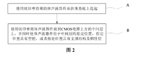
- FIG. 2 is a schematic flowchart of a heterogeneous integration method for an air gap piezoelectric bulk acoustic wave device according to an embodiment of the present invention
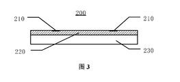
- FIG. 3 is a cross-sectional view of the main structure of the oscillator circuit in the heterogeneous integrated device of the embodiment of the present invention.
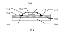
- FIG. 4 is a cross-sectional view of an air gap type piezoelectric bulk acoustic wave device heterogeneous integrated device according to the first embodiment of the present invention
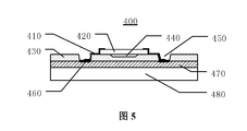
- FIG. 5 is a cross-sectional view of an air gap type piezoelectric bulk acoustic wave device heterogeneous integrated device according to a second embodiment of the present invention.
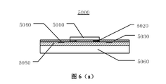
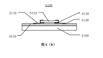
- 6(a) and 6(b) are respectively the cross-sectional views of the processing intermediate state and the final state of the air gap type piezoelectric bulk acoustic wave device heterogeneous integrated device according to the third embodiment of the present invention.
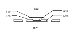
- FIG. 7 is a cross-sectional view of a partial structure of the adhesion layer integration of the air gap type piezoelectric bulk acoustic wave device heterogeneous integrated device according to the fourth embodiment of the present invention.
- first and second are only used for descriptive purposes, and cannot be understood as indicating or implying relative importance or implicitly indicating the number of indicated technical features. Thus, the features defined with “first” and “second” may explicitly or implicitly include one or more of these features. In the description of the present invention, “plurality” means two or more than two, unless specifically defined otherwise.
- the terms “installed”, “connected”, “connected”, “fixed” and other terms should be understood in a broad sense, for example, it can be a fixed connection or a detachable connection. , Or integrally connected; it can be a mechanical connection or an electrical connection; it can be directly connected, or indirectly connected through an intermediate medium, and it can be the internal communication between two components.
- installed can be a fixed connection or a detachable connection.
- it can be a mechanical connection or an electrical connection
- it can be directly connected, or indirectly connected through an intermediate medium, and it can be the internal communication between two components.
- the specific meaning of the above-mentioned terms in the present invention can be understood according to specific circumstances.
- the "above” or “below” of the first feature of the second feature may include the first and second features in direct contact, or may include the first and second features Not in direct contact but through other features between them.
- “above”, “above” and “above” the second feature of the first feature include the first feature being directly above and obliquely above the second feature, or it simply means that the level of the first feature is higher than the second feature.
- the “below”, “below” and “below” the first feature of the second feature include the first feature directly below and obliquely below the second feature, or it simply means that the level of the first feature is smaller than the second feature.
- FIG. 2 is a schematic flowchart of a heterogeneous integration method of an air gap piezoelectric bulk acoustic wave device according to an embodiment of the present invention.
- the method includes: A. using a soft seal to lift the bulk acoustic wave device film from the donor substrate; B. using the soft seal to place the bulk acoustic wave device on the intermediate layer above the CMOS circuit, At the same time, the bulk acoustic wave device is located at a designated position of the intermediate layer, the designated position has a cavity, or the designated position has a supporting structure and a sacrificial layer.
- the bulk acoustic wave device film here refers to a completely unencapsulated bulk acoustic wave device with a thickness of only a few microns, and the thickness is much smaller than that of similar packaged devices.
- the air gap type piezoelectric bulk acoustic wave device heterogeneous integration method of the present invention uses material transfer printing technology to transfer the transferable bulk acoustic wave device to the target system platform, and finally forms a 3D stacked integrated structure.
- the advantages of this method include at least the following aspects: (1) Lower cost. This method directly operates the bulk acoustic wave device film, and the process is more simplified. (2) Higher integration. The film-like bulk acoustic wave device film itself has the characteristics of small size and light weight, the thickness is one to two orders of magnitude smaller than the corresponding device in the conventional integration method, and the space occupation rate is less than the traditional 2D and 3D integrated layout. (3) Lower operating temperature requirements.
- the transfer printing technology is used to integrate the piezoelectric bulk acoustic wave device with a transferable structure, and the operation can be completed at a lower temperature, avoiding high temperature requirements such as traditional bonding. (4) Shorter operating time. Compared with traditional bonding and other operations, the transfer process and its alignment and other operations take less time.
- piezoelectric bulk acoustic wave devices are not limited to FBAR, but also include but are not limited to other types of bulk acoustic wave devices, such as Piezoelectric Micromachined Ultrasonic Transducers (PMUT), Lamb wave resonators (Lamb Wave Resonator, LWR), MEMS microphones, etc.
- CMOS integrated circuits include, but are not limited to, oscillator circuits, and can also be filter circuits, duplexer circuits, and the like.
- the transfer target system is not limited to CMOS integrated circuits, but also includes but not limited to gallium arsenide (GaAs), gallium nitride (GaN), silicon carbide (SiC), diamond, lithium niobate, tantalum Electronic components based on lithium tantalate and quartz.
- GaAs gallium arsenide
- GaN gallium nitride
- SiC silicon carbide
- diamond lithium niobate
- the main structure 200 of the oscillator circuit (CMOS integrated circuit) involved in the following embodiments includes: an electrode plate 210, a CMOS circuit 220 and a silicon substrate 230.
- the electrode plate 210 is used to establish an electrical connection with the outside (including the connection with the FBAR).
- FBAR is additionally processed by MEMS technology, and its core structure is a sandwich structure composed of electrodes on both sides and a piezoelectric layer located between the electrodes.
- the FBAR electrode is any one of the following: osmium, magnesium, gold, tungsten, molybdenum, platinum, ruthenium, iridium, germanium, copper, titanium, titanium tungsten, aluminum, chromium, and arsenic-doped gold.
- the material of the FBAR piezoelectric layer is any one of the following: aluminum nitride, zinc oxide, lead zirconate titanate, lithium niobate, quartz, potassium niobate, and lithium tantalate.
- the material of the piezoelectric layer is aluminum nitride doped with rare earth elements.
- the aforementioned material is a piezoelectric film with a thickness of less than 10 microns.
- the aluminum nitride film is in a polycrystalline form or a single crystal form, and the growth method is thin film sputtering or metal organic chemical vapor deposition (MOCVD).
- the FBAR body is connected to the wafer by anchor points and has transferability characteristics.
- the soft stamps used for transfer are generally made of viscoelastic materials, such as polydimethylsiloxane (PDMS).
- an intermediate layer with a cavity structure is formed above the CMOS circuit, and then device transfer is performed.
- the intermediate layer material is added to the top of the CMOS circuit by conventional methods such as spin coating or deposition;
- the cavity structure and the electrode plate window are formed directly through the photolithography process or photolithography and etching process, and the electrode plate window makes the electrode plate exposed ;
- use the transfer printing method to transfer the FBAR above the cavity and establish an electrical connection with the CMOS circuit.
- the resulting structure 300 is shown in FIG. 4, including: a metal conductive film 310, an FBAR device 320, an intermediate layer 330, a cavity structure 340 on the intermediate layer, an electrode plate window 350, an electrode plate 360, a CMOS circuit 370, and a silicon substrate 380 .
- the material of the intermediate layer includes, but is not limited to, silicon dioxide (SiO 2 ), silicon nitride (Si 3 N 4 ), organic polymers (Polymer) such as polyimide (PI) and the like.
- SiO 2 silicon dioxide
- Si 3 N 4 silicon nitride
- Polymer organic polymers
- PI polyimide
- the electrical connection between the FBAR and the CMOS circuit can also be achieved by wire bonding.
- the material of the cavity layer is semi-solid UV glue, which can be easily pasted on a specified surface, has a plastic shape, and can produce irreversible curing when irradiated by ultraviolet light.
- the resulting structure is shown in Figure 5, the structural unit 400 from top to bottom is the metal conductive film 410, the FBAR device 420, the UV glue layer 430, the cavity structure 440 on the UV glue layer, the electrode plate window 450, and the electrode plate. 460, CMOS circuit 470 and silicon substrate 480.
- the cavity structure is imprinted by the hot embossing method.
- the specific method is to cover the transparent hard material with convex structure, such as glass, on the UV glue, and continue to apply a certain pressure and The temperature is then irradiated with ultraviolet light for a short period of time. The short period of irradiation causes the UV glue to be incompletely cured, and the hard material is separated but maintains a certain viscosity. After removing the hard material, perform the transfer operation, and then irradiate with ultraviolet light to completely cure the UV glue. Finally, an electrical connection is established between the CMOS circuit and the FBAR.
- the electrical connection in addition to depositing a metal film, the electrical connection can also be achieved by wire bonding.
- the FBAR structure is suspended by establishing a supporting structure, thereby building an acoustic reflection interface at the bottom.
- the support structure and the sacrificial layer are first established, and then the FBAR is transferred to the top of the support structure.
- the resulting structure is shown in Figure 6(a).
- the structural unit 5000 includes: an FBAR device 5010, a supporting structure 5020, a sacrificial layer 5030, an electrode plate 5040, a CMOS circuit 5050, and a silicon substrate 5060.
- the sacrificial layer material is released, so that the effective resonance area of the FBAR is suspended and an electrical connection between the FBAR and the CMOS circuit is established.
- the structure 5100 includes: a metal conductive film 5110, an FBAR device 5120, a supporting structure 5130, an electrode plate 5140, a CMOS circuit 5150, and a silicon substrate 5160.
- the support material includes but is not limited to silicon dioxide (SiO 2 ), silicon nitride (Si 3 N 4 ), organic polymers (Polymer) such as polyimide (PI), etc., sacrificial layer materials Including but not limited to silicon dioxide (SiO 2 ) and the like. It should be noted that the sacrificial layer release process should not cause etching and other effects on the support structure. Electrical connection methods include but are not limited to metal film deposition, wire bonding, and so on.
- an adhesion layer is introduced between the cavity structure and the FBAR to make the connection between the cavity structure and the FBAR more reliable.
- the partial structure of the integration containing the adhesion layer is shown in FIG. 7, the structural unit 600 includes the FBAR device 610, the adhesion layer 620 and the intermediate layer 640 with the cavity structure 630 from top to bottom.
- the adhesion layer can be applied in the third embodiment, and the adhesion layer is located on the supporting structure in the third embodiment.
- the adhesion layer has thermosetting properties.
- the adhesion layer is heated and cured after the FBAR is transferred to form a stable and reliable connection.
- the formation of the adhesion layer is not unique.
- the adhesion layer that is initially liquid it can be coated on a thin layer by spin coating or 3D printing, and the solvent is evaporated after the transfer is completed. In order to speed up the solvent evaporation process, the entire platform can be heated without damaging the circuit structure.
- the adhesion layer material includes, but is not limited to, ethyl cellulose (EC), benzocyclobutene (BCB), organic solution mixtures (such as PI and N-methylpyrrolidone) and the like.
- EC ethyl cellulose
- BCB benzocyclobutene
- organic solution mixtures such as PI and N-methylpyrrolidone
- the invention also proposes a heterogeneous integrated air gap piezoelectric bulk acoustic wave device, which is prepared by the method of the invention.
- the heterogeneous integrated air-gap piezoelectric bulk acoustic wave device of the embodiment of the present invention may be as shown in FIG. 4, including: a substrate, a CMOS circuit located above the substrate, and an intermediate layer with a cavity located above the CMOS circuit.
- the heterogeneous integrated air-gap piezoelectric bulk acoustic wave device of the embodiment of the present invention may be as shown in FIG. 5, including: a substrate, a CMOS circuit located above the substrate, and a UV adhesive layer with a cavity located above the CMOS circuit.
- the heterogeneous integrated air-gap piezoelectric bulk acoustic wave device of the embodiment of the present invention may be shown in FIG. 6(b), including: a substrate, a CMOS circuit located above the substrate, a support structure located above the CMOS circuit, and a support structure located above the support structure The bulk acoustic wave device film, and the electrode plate.
- an adhesion layer (as shown in FIG. 7) is provided on the intermediate layer or an adhesion layer is provided on the support structure.
Landscapes
- Physics & Mathematics (AREA)
- Acoustics & Sound (AREA)
- Engineering & Computer Science (AREA)
- Manufacturing & Machinery (AREA)
- Piezo-Electric Or Mechanical Vibrators, Or Delay Or Filter Circuits (AREA)
Abstract
提供一种空气隙型压电体声波器件异质集成方法,包括:使用软印章将体声波器件薄膜(320)从供体基底上提起;使用软印章将体声波器件放到CMOS电路(370)上方的中间层(330)上,并同时使体声波器件位于中间层的指定位置,指定位置具有空腔(340),或者指定位置具有支撑结构(5020)及牺牲层(5030)。运用材料转移印刷技术将可转移体声波器件转移至目标系统平台上,最终形成3D堆叠式集成结构,优势在于:更低的成本、更高的集成度、更低的操作温度要求以及更短的操作时间。
Description
本发明涉及半导体技术领域,特别地涉及一种空气隙型压电体声波器件异质集成方法和该器件。
异质集成(Heterogeneous Integration,HI)是指仅在一个系统平台上就能实现集成的技术,它通过一系列过程制造并组装成完整的电子子系统,如MEMS(Micro-Electro-Mechanical System)器件、SOI/CMOS混合信号专用集成电路(ASIC)、微尺度无源组件和微功率系统等。异质集成被认为是实现片上系统(System-on-Chip,SoC)和系统级封装(System-on-a-Package,SoP)的关键策略。与此同时,以III-V族元素化合物、碳纳米管等为代表的高性能新型应用已越来越广泛。若将基于这些高性能材料的电子组件与传统硅基互补式金属氧化物半导体(CMOS)电路集成在一起则可以进一步获得集成度更高、性能更优的电子系统,这对集成电路在延续摩尔定律方面具有重要意义。事实上,以上所提及的高性能材料在某些工序上多不与传统CMOS工艺相兼容,这种情况下相应的电子组件往往需要独立制造,然后通过异质集成手段将他们组建在同一个系统平台上。
现有的异质集成手段主要分为两类:混合集成和单片集成。混合集成是将工艺不兼容的电子组件分别制造,然后进行系统级或晶圆级电学连接。此过程中需要将其中一种组件连同其基底进行翻转,将连接突起点对准后进行键合。键合过程使得连个接触体间建立分子级的稳固连接而成为一体,最后去除不必要的基底,但该过程往往需要在高温条件才能完成,高温可能损害某些电子组件。单片集成适用于工艺差异不太大的异质集成中,当一部分组件制造结束后,在其表面建 立电学连接端并形成连接和特定的保护层,然后直接在此基础上进行第二部分组件的加工。
另一方面,基于压电材料的体声波谐振器正在吸引人们的研究注意力。由体声波谐振器构成的射频前端滤波器/双工器具有优越的滤波特性,例如低插入损耗、陡峭的过渡带、较大的功率容量和较强的抗静电放电(ESD)能力。具有超低频率温度漂移的高频体声波振荡器,其相位噪声低、功耗低且带宽调制范围大。除此之外,这些微型体声波谐振器可由MEMS工艺在硅衬底上大量制备,从而降低了单位成本。以薄膜体声波谐振器(Film Bulk Acoustic Resonator,FBAR)为例,其结构示意如图1所示,谐振器具有典型的“三明治”结构,从上至下依次为顶电极110、压电层120和底电极130。当两电极间被施加射频电压时,压电层在厚度方向上被激发出体声波并伴随微小形变,声波能量在谐振器结构体中损耗或传播,到达边界面时则透射到另一介质或被反射回来,最终形成驻波,即进入谐振状态。在进行体声波谐振器设计时,为了最大程度上减少声能量损失,除了选用低声损耗材料等措施外,更应注重构建一个高声反射率界面。空气隙型结构常被用作高声反射率声反射面,这是因为空气与谐振体材料的声阻抗特性在数量级上具有较大差异,从而导致声反射率极高。空气隙型结构可以通过谐振体有效谐振区域厚度方向上在衬底材料150构造空腔140结构实现,如图1所示,发生谐振时,体声波在顶电极上表面、底电极下表面与有效谐振区域共同围成的区域内传播。注意,这里的有效谐振区域定义为顶电极、压电层和底电极三层材料在厚度方向上重叠的区域。
根据上述现有异质集成方法,难以实现压电体声波器件薄膜的异质集成。压电体声波器件薄膜指未加外围结构保护措施的压电体声波谐振器,即只包含顶电极、压电层、底电极和必要的金属导电层。与其它形式的压电体声波谐振器相比,由于未加以塑封等保护,压电体声波器件薄膜整体保留了薄膜结构,所占用体积很小,易获得更高的 集成度。首先,混合集成中的键合工艺不适用于谐振器材料且高温可能会对谐振器造成性能损害。其次,即便在有保护层的情况下进行,直接采用单片集成的方式也容易引起CMOS电路受损且工艺复杂。目前,在涉及大量制备的前提下,尚无针对压电体声波器件薄膜的高效异质集成方法。
发明内容
有鉴于此,本发明旨在提供一种空气隙型压电体声波器件异质集成方法,具有简单易行、高效可靠的优点。
本发明的空气隙型压电体声波器件薄膜的异质集成方法,包括:使用软印章将体声波器件薄膜从供体基底上提起;使用所述软印章将所述体声波器件放到CMOS电路上方的中间层上,并同时使所述体声波器件位于所述中间层的指定位置,所述指定位置具有空腔,或者所述指定位置具有支撑结构及牺牲层。
可选地,所述中间层为半固态的UV胶。
可选地,所述指定位置具有空腔,并且使用所述软印章将所述体声波器件放到CMOS电路上方的中间层上的步骤之前,还包括:在中间层上形成黏附层。
可选地,所述指定位置具有支撑结构及牺牲层,并且使用所述软印章将所述体声波器件放到CMOS电路上方的中间层上的步骤之前,还包括:在支撑结构上形成黏附层。
可选地,在使用所述软印章将所述体声波器件放到CMOS电路上方的中间层上的步骤之后,还包括:去除所述牺牲层,以形成空腔。
可选地,所述中间层和所述支撑结构的材料包括但不限于:二氧 化硅、氮化硅或有机聚合物。
可选地,所述牺牲层的材料包括但不限于二氧化硅。
可选地,所述体声波器件与CMOS电路之间的电学连接方式包括但不限于沉积金属薄膜或引线键合。
可选地,所述CMOS电路基于如下材料的器件基底上:砷化镓、氮化镓、碳化硅、金刚石、铌酸锂、钽酸锂或石英。
可选地,所述黏附层的材料包括但不限于乙基纤维素、苯并环丁烯或有机溶液混合物。
本发明的空气隙型压电体声波器件异质集成方法,运用材料转移印刷技术将可转移体声波器件转移至目标系统平台上,最终形成3D堆叠式集成结构。该方法的优势至少包括以下几个方面:(1)更低的成本。该方法直接对体声波器件薄膜进行操作,工序更加简化。(2)更高的集成度。薄膜状体声波器件薄膜自身具有体积小、质量轻特点,厚度比常规集成方法中的对应器件小一到两个数量级,且与传统2D和3D集成布局相比空间占用率更少。(3)更低的操作温度要求。利用转移印刷技术对具有可转移结构的压电体声波器件进行集成,操作可在较低温度内完成,避免了传统键合等高温要求。(4)更短的操作时间。与传统键合等操作相比,转移过程及其对准等操作耗时更短。
本发明还提出一种异质集成的空气隙型压电体声波器件,它是通过本发明的方法所制备的。
本发明的异质集成的空气隙型压电体声波器件可以包括:基底、位于所述基底上方的CMOS电路、位于所述CMOS电路上方的具有空腔的中间层,位于空腔上方的体声波器件薄膜,以及电极板、电极板 窗口和金属导电薄膜。
本发明的异质集成的空气隙型压电体声波器件可以包括:基底、位于所述基底上方的CMOS电路、位于所述CMOS电路上方的具有空腔的UV胶层,位于空腔上方的体声波器件薄膜,以及电极板、电极板窗口和金属导电薄膜。
本发明的异质集成的空气隙型压电体声波器件可以包括:基底、位于所述基底上方的CMOS电路,位于所述CMOS电路上方的支撑结构,位于所述支撑结构上方的体声波器件薄膜,以及电极板。
本发明的异质集成的空气隙型压电体声波器件中,所述中间层之上具有黏附层或者所述支撑结构之上具有黏附层。
附图用于更好地理解本发明,不构成对本发明的不当限定。其中:
图1是具有典型的“三明治”结构薄膜体声波谐振器的结构示意图。
图2是本发明实施例的空气隙型压电体声波器件异质集成方法的流程示意图;
图3是本发明实施例的异质集成器件中的振荡器电路主体结构的剖面图;
图4是本发明第一实施例的空气隙型压电体声波器件异质集成器件的剖面图;
图5是本发明第二实施例的空气隙型压电体声波器件异质集成器件的剖面图;
图6(a)和图6(b)分别是本发明第三实施例空气隙型压电体声波器件异质集成器件的加工中间态和终态的剖面图;
图7是本发明第四实施例的空气隙型压电体声波器件异质集成器件的黏附层集成的局部结构的剖面图。
下面详细描述本发明的实施例,所述实施例的示例在附图中示出,其中自始至终相同或类似的标号表示相同或类似的元件或具有相同或类似功能的元件。下面通过参考附图描述的实施例是示例性的,旨在用于解释本发明,而不能理解为对本发明的限制。
在本发明的描述中,需要理解的是,术语“中心”、“纵向”、“横向”、“长度”、“宽度”、“厚度”、“上”、“下”、“前”、“后”、“左”、“右”、“竖直”、“水平”、“顶”、“底”“内”、“外”、“顺时针”、“逆时针”等指示的方位或位置关系为基于附图所示的方位或位置关系,仅是为了便于描述本发明和简化描述,而不是指示或暗示所指的装置或元件必须具有特定的方位、以特定的方位构造和操作,因此不能理解为对本发明的限制。
此外,术语“第一”、“第二”仅用于描述目的,而不能理解为指示或暗示相对重要性或者隐含指明所指示的技术特征的数量。由此,限定有“第一”、“第二”的特征可以明示或者隐含地包括一个或者更多个该特征。在本发明的描述中,“多个”的含义是两个或两个以上,除非另有明确具体的限定。
在本发明中,除非另有明确的规定和限定,术语“安装”、“相连”、“连接”、“固定”等术语应做广义理解,例如,可以是固定连接,也可以是可拆卸连接,或一体地连接;可以是机械连接,也可以是电连接;可以是直接相连,也可以通过中间媒介间接相连,可以是两个元件内部的连通。对于本领域的普通技术人员而言,可以根据具体情况理解上述术语在本发明中的具体含义。
在本发明中,除非另有明确的规定和限定,第一特征在第二特征之“上”或之“下”可以包括第一和第二特征直接接触,也可以包括 第一和第二特征不是直接接触而是通过它们之间的另外的特征接触。而且,第一特征在第二特征“之上”、“上方”和“上面”包括第一特征在第二特征正上方和斜上方,或仅仅表示第一特征水平高度高于第二特征。第一特征在第二特征“之下”、“下方”和“下面”包括第一特征在第二特征正下方和斜下方,或仅仅表示第一特征水平高度小于第二特征。
图2是本发明实施例的空气隙型压电体声波器件异质集成方法的流程示意图。如图2所示,该方法包括:A.使用软印章将体声波器件薄膜从供体基底上提起;B.使用所述软印章将所述体声波器件放到CMOS电路上方的中间层上,并同时使所述体声波器件位于所述中间层的指定位置,所述指定位置具有空腔,或者所述指定位置具有支撑结构及牺牲层。这里的体声波器件薄膜是指厚度仅为几微米的完全未封装的体声波器件,厚度远小于封装了的同类器件。
本发明的空气隙型压电体声波器件异质集成方法,运用材料转移印刷技术将可转移体声波器件转移至目标系统平台上,最终形成3D堆叠式集成结构。该方法的优势至少包括以下几个方面:(1)更低的成本。该方法直接对体声波器件薄膜进行操作,工序更加简化。(2)更高的集成度。薄膜状体声波器件薄膜自身具有体积小、质量轻特点,厚度比常规集成方法中的对应器件小一到两个数量级,且与传统2D和3D集成布局相比空间占用率更少。(3)更低的操作温度要求。利用转移印刷技术对具有可转移结构的压电体声波器件进行集成,操作可在较低温度内完成,避免了传统键合等高温要求。(4)更短的操作时间。与传统键合等操作相比,转移过程及其对准等操作耗时更短。
本发明涉及的所有实施例以FBAR与振荡器CMOS集成电路间的异质集成为例展开叙述。需要说明的是,压电体声波器件不限于FBAR,还包括但不局限于其它类型的体声波器件,如压电微机械超声换能器(Piezoelectric Micromachined Ultrasonic Transducers,PMUT)、兰姆波 谐振器(Lamb Wave Resonator,LWR)、MEMS麦克风等。CMOS集成电路包括但不限于振荡器电路,还可以是滤波器电路、双工器电路等。转移目标系统不局限于CMOS集成电路,还包括但不限于基于砷化镓(GaAs)、氮化镓(GaN)、碳化硅(SiC)、金刚石(diamond)、铌酸锂(lithium niobate)、钽酸锂(lithium tantalate)、石英(quartz)等基底的电子元器件。
如图3所示,以下实施例中所涉及的振荡器电路(CMOS集成电路)主体结构200包括:电极板210、CMOS电路220和硅基底230。其中,电极板210用于与外界建立电学连接(包括与FBAR之间的连接)。FBAR由MEMS工艺另外加工得到,其核心结构为由两侧电极和位于电极间的压电层构成的三明治结构。所述FBAR电极为以下任意一种:锇、镁、金、钨、钼、铂、钌、铱、锗、铜、钛、钛钨、铝、铬、砷掺杂金。可选的,所述FBAR压电层的材料为以下任意一种:氮化铝、氧化锌、锆钛酸铅、铌酸锂、石英、铌酸钾、钽酸锂。可选的,所述压电层的材料为掺杂稀土元素的氮化铝。上述材料为压电薄膜,厚度小于10微米。氮化铝薄膜为多晶形态或者单晶形态,生长方式为薄膜溅射(sputtering)或者有机金属化学气相沉积法(MOCVD)。
FBAR主体通过锚点连接在晶圆上且具有可转移特性。用于转移的软印章一般由具有黏弹性的材料制作得到,如聚二甲基硅氧烷(Polydimethylsiloxane,PDMS)等。
转移时,先用软印章将FBAR器件薄膜从供体基底(例如硅晶圆)上提起,这个过程中用于束缚FBAR的锚点结构发生断裂,FBAR与软印章粘附在一起。其次,将携带了FBAR的软印章与振荡器电路上的空腔结构对齐,向下移动软印章使FBAR底面与空腔有接触。最后,缓慢提起软印章,FBAR与软印章分离并黏附在振荡器电路上。所述转移操作可阵列化大批量进行。
为使本领域技术人员更好地理解,下面结合具体实施例进行说明。
实施例1
本实施例中,在CMOS电路上方形成带空腔结构的中间层,然后进行器件转移。
首先,中间层材料通过旋涂或沉积等常规方法被添加到CMOS电路上方;其次,直接通过光刻工艺或者光刻加刻蚀工艺形成空腔结构及电极板窗口,电极板窗口使得电极板露出;最后,利用转移印刷方法将FBAR转移至空腔上方并与CMOS电路建立电学连接。得到的结构300如图4所示,包括:金属导电薄膜310、FBAR器件320、中间层330、中间层上的空腔结构340、电极板窗口350、电极板360、CMOS电路370和硅基底380。
本实施例中,中间层材料包括但不限于二氧化硅(SiO
2)、氮化硅(Si
3N
4)、有机聚合物(Polymer)如聚乙酰亚胺(Polyimide,PI)等。FBAR与CMOS电路之间的电学连接方式除了金属导电薄膜,还可以通过引线键合(Wire bonding)等方式实现。
实施例2
本实施例中,使用UV胶和热压印的实现可靠集成。空腔层的材料为半固态的UV胶,其特性是可被方便地粘贴在指定的面上、形状可塑且被紫外光照射时能够产生不可逆的固化。最终获得的结构如图5所示,结构单元400从上至下依次为金属导电薄膜410、FBAR器件420、UV胶层430、UV胶层上的空腔结构440、电极板窗口450、电极板460、CMOS电路470和硅基底480。
UV胶被粘贴在CMOS电路表面后,用热压印方法压印出空腔结构,具体做法是:在UV胶上方覆盖带凸起结构的透光硬质材料,如玻璃,持续施加一定压力和温度,之后用紫外光短时照射,短时照射使得UV胶发生不完全固化,硬质材料分离但又维持一定黏性。移去硬质材料后进行转移操作,然后再用紫外光照射,使UV胶完全固化。最后,在CMOS电路和FBAR之间建立电学连接。
本实施例中,电学连接方式除了沉积金属薄膜,还可以通过引线 键合等方式实现。
实施例3
本实施例中,通过建立支撑结构使得FBAR结构悬空,从而在底部构建声反射界面。支撑结构和牺牲层首先被建立,然后将FBAR转移至支撑结构上方,形成的结构如图6(a)所示。图6(a)中,结构单元5000包括:FBAR器件5010、支撑结构5020、牺牲层5030、电极板5040、CMOS电路5050和硅基底5060。最后将牺牲层材料释放,使FBAR有效谐振区域悬空并建立FBAR与CMOS电路之间的电学连接,最终形成的结构如图6(b)所示。图6(b)中,结构5100包括:金属导电薄膜5110、FBAR器件5120、支撑结构5130、电极板5140、CMOS电路5150和硅基底5160。
本实施例中,支撑材料包括但不限于二氧化硅(SiO
2)、氮化硅(Si
3N
4)、有机聚合物(Polymer)如聚乙酰亚胺(Polyimide,PI)等,牺牲层材料包括但不限于二氧化硅(SiO
2)等。需要注意的牺牲层释放工艺不应对支撑结构造成刻蚀等影响。电学连接方式包括但不限于沉积金属薄膜、引线键合等。
实施例4
本实施例中,在空腔结构与FBAR之间引入黏附层,旨在使得空腔结构与FBAR之间的连接更加可靠。含黏附层集成的局部结构示意如图7,结构单元600从上至下依次为FBAR器件610、黏附层620和带空腔结构630的中间层640。另可以在实施例3中应用黏附层,此时黏附层位于实施例3中的支撑结构上。
本实施例中,黏附层具有热固性。黏附层在FBAR转移后被加热固化,从而形成稳定可靠的连接关系。黏附层的形成方式不唯一,对于初始状态为液态的黏附层,可将通过黏附液旋涂或3D打印等方式将其涂覆于薄层上,转移完成后再将溶剂蒸发。为了加快溶剂蒸发进程,可在不损坏电路结构的前提下对平台整体进行加热。
本实施例中,黏附层材料包括但不限于乙基纤维素(EC)、苯并 环丁烯(BCB)、有机溶液混合物(如PI和N-甲基吡咯烷酮)等。
本发明还提出了异质集成的空气隙型压电体声波器件,它是通过本发明的方法所制备的。
本发明实施例的异质集成的空气隙型压电体声波器件可以如图4所示,包括:基底、位于基底上方的CMOS电路、位于CMOS电路上方的具有空腔的中间层,位于空腔上方的体声波器件薄膜,以及电极板、电极板窗口和金属导电薄膜。
本发明实施例的异质集成的空气隙型压电体声波器件可以如图5所示,包括:基底、位于基底上方的CMOS电路、位于CMOS电路上方的具有空腔的UV胶层,位于空腔上方的体声波器件薄膜,以及电极板、电极板窗口和金属导电薄膜。
本发明实施例的异质集成的空气隙型压电体声波器件可以如图6(b)所示,包括:基底、位于基底上方的CMOS电路,位于CMOS电路上方的支撑结构,位于支撑结构上方的体声波器件薄膜,以及电极板。
本发明实施例的异质集成的空气隙型压电体声波器件中,中间层之上具有黏附层(如图7所示)或者支撑结构之上具有黏附层。
上述具体实施方式,并不构成对本发明保护范围的限制。本领域技术人员应该明白的是,取决于设计要求和其他因素,可以发生各种各样的修改、组合、子组合和替代。任何在本发明的精神和原则之内所作的修改、等同替换和改进等,均应包含在本发明保护范围之内。
Claims (15)
- 一种空气隙型压电体声波器件异质集成方法,其特征在于,包括:使用软印章将体声波器件薄膜从供体基底上提起;使用所述软印章将所述体声波器件放到CMOS电路上方的中间层上,并同时使所述体声波器件位于所述中间层的指定位置,所述指定位置具有空腔,或者所述指定位置具有支撑结构及牺牲层。
- 根据权利要求1所述的方法,其特征在于,所述中间层为半固态的UV胶。
- 根据权利要求1所述的方法,其特征在于,所述指定位置具有空腔,并且使用所述软印章将所述体声波器件放到CMOS电路上方的中间层上的步骤之前,还包括:在中间层上形成黏附层。
- 根据权利要求1所述的方法,其特征在于,所述指定位置具有支撑结构及牺牲层,并且使用所述软印章将所述体声波器件放到CMOS电路上方的中间层上的步骤之前,还包括:在支撑结构上形成黏附层。
- 根据权利要求1或4所述的方法,其特征在于,在使用所述软印章将所述体声波器件放到CMOS电路上方的中间层上的步骤之后,还包括:去除所述牺牲层,以形成空腔。
- 根据权利要求1所述的方法,其特征在于,所述中间层和所述支撑结构的材料包括但不限于:二氧化硅、氮化硅或有机聚合物。
- 根据权利要求1所述的方法,其特征在于,所述牺牲层的材料包括二氧化硅。
- 根据权利要求1所述的方法,其特征在于,所述体声波器件与CMOS电路之间的电学连接方式包括沉积金属薄膜或引线键合。
- 根据权利要求1所述的方法,其特征在于,所述CMOS电路基于如下材料的器件基底上:砷化镓、氮化镓、碳化硅、金刚石、铌酸锂、钽酸锂或石英。
- 根据权利要求4或5的方法,其特征在于,所述黏附层的材料包括但不限于乙基纤维素、苯并环丁烯或有机溶液混合物。
- 一种异质集成的空气隙型压电体声波器件,其特征在于,所述空气隙型压电体声波器件是通过权利要求1至10中任一项所述的方法所制备。
- 一种异质集成的空气隙型压电体声波器件,其特征在于,包括:基底、位于所述基底上方的CMOS电路、位于所述CMOS电路上方的具有空腔的中间层,位于空腔上方的体声波器件薄膜,以及电极板、电极板窗口和金属导电薄膜。
- 一种异质集成的空气隙型压电体声波器件,其特征在于,包括:基底、位于所述基底上方的CMOS电路、位于所述CMOS电路上方的具有空腔的UV胶层,位于空腔上方的体声波器件薄膜,以及电极板、电极板窗口和金属导电薄膜。
- 一种异质集成的空气隙型压电体声波器件,其特征在于,包括:基底、位于所述基底上方的CMOS电路,位于所述CMOS电路上方的支撑结构,位于所述支撑结构上方的体声波器件薄膜,以及电极板。
- 根据权利要求13或14所述的异质集成的空气隙型压电体声 波器件,其特征在于,所述中间层之上具有黏附层或者所述支撑结构之上具有黏附层。
Priority Applications (1)
| Application Number | Priority Date | Filing Date | Title |
|---|---|---|---|
| PCT/CN2018/124074 WO2020163973A1 (zh) | 2019-02-15 | 2019-02-15 | 一种空气隙型压电体声波器件异质集成方法和该器件 |
Applications Claiming Priority (1)
| Application Number | Priority Date | Filing Date | Title |
|---|---|---|---|
| PCT/CN2018/124074 WO2020163973A1 (zh) | 2019-02-15 | 2019-02-15 | 一种空气隙型压电体声波器件异质集成方法和该器件 |
Publications (1)
| Publication Number | Publication Date |
|---|---|
| WO2020163973A1 true WO2020163973A1 (zh) | 2020-08-20 |
Family
ID=72044933
Family Applications (1)
| Application Number | Title | Priority Date | Filing Date |
|---|---|---|---|
| PCT/CN2018/124074 Ceased WO2020163973A1 (zh) | 2019-02-15 | 2019-02-15 | 一种空气隙型压电体声波器件异质集成方法和该器件 |
Country Status (1)
| Country | Link |
|---|---|
| WO (1) | WO2020163973A1 (zh) |
Citations (5)
| Publication number | Priority date | Publication date | Assignee | Title |
|---|---|---|---|---|
| CN102545827A (zh) * | 2012-01-04 | 2012-07-04 | 华为技术有限公司 | 薄膜体声波谐振器、通信器件和射频模块 |
| CN104030234A (zh) * | 2014-06-04 | 2014-09-10 | 江苏艾伦摩尔微电子科技有限公司 | 基于薄膜体声波谐振器的mems红外传感器制备方法 |
| CN105355563A (zh) * | 2015-11-26 | 2016-02-24 | 上海集成电路研发中心有限公司 | 一种柔性半导体器件的制备方法 |
| CN105680813A (zh) * | 2016-02-25 | 2016-06-15 | 锐迪科微电子(上海)有限公司 | 一种薄膜体声波谐振器及其制造方法 |
| CN107093994A (zh) * | 2017-03-24 | 2017-08-25 | 杭州左蓝微电子技术有限公司 | 薄膜体声波谐振器及其加工方法 |
-
2019
- 2019-02-15 WO PCT/CN2018/124074 patent/WO2020163973A1/zh not_active Ceased
Patent Citations (5)
| Publication number | Priority date | Publication date | Assignee | Title |
|---|---|---|---|---|
| CN102545827A (zh) * | 2012-01-04 | 2012-07-04 | 华为技术有限公司 | 薄膜体声波谐振器、通信器件和射频模块 |
| CN104030234A (zh) * | 2014-06-04 | 2014-09-10 | 江苏艾伦摩尔微电子科技有限公司 | 基于薄膜体声波谐振器的mems红外传感器制备方法 |
| CN105355563A (zh) * | 2015-11-26 | 2016-02-24 | 上海集成电路研发中心有限公司 | 一种柔性半导体器件的制备方法 |
| CN105680813A (zh) * | 2016-02-25 | 2016-06-15 | 锐迪科微电子(上海)有限公司 | 一种薄膜体声波谐振器及其制造方法 |
| CN107093994A (zh) * | 2017-03-24 | 2017-08-25 | 杭州左蓝微电子技术有限公司 | 薄膜体声波谐振器及其加工方法 |
Similar Documents
| Publication | Publication Date | Title |
|---|---|---|
| CN109257026A (zh) | 柔性基底薄膜体声波谐振器及其形成方法 | |
| US8698376B2 (en) | Microelectromechanical systems (MEMS) resonators and related apparatus and methods | |
| CN202026284U (zh) | 预设空腔型soi基片薄膜体声波谐振器 | |
| CN111245397A (zh) | 体声波谐振器及制造方法、体声波谐振器单元、滤波器及电子设备 | |
| CN112039486A (zh) | 薄膜体声波谐振器及其制造方法 | |
| CN103929149B (zh) | 一种柔性压电薄膜体声波谐振器及其制备方法 | |
| CN112803910A (zh) | 一种单晶薄膜体声波谐振器的制备方法 | |
| CN108092639A (zh) | 一种微纳米柱柔性阵列薄膜体声波谐振子滤波器及其制备 | |
| CN101977026A (zh) | 一种空腔型薄膜体声波谐振器(fbar)的制作方法 | |
| CN102545814A (zh) | 用于制造包括悬浮隔膜的声波谐振器的方法 | |
| CN111756351B (zh) | 体声波谐振器及其制造方法、滤波器和电子设备 | |
| JP2021503229A (ja) | 圧電共振器および圧電共振器の製造方法 | |
| WO2020132997A1 (zh) | 单晶压电薄膜体声波谐振器及其形成方法 | |
| CN114337585B (zh) | 一种单晶薄膜体声波谐振器及其制备方法、滤波器 | |
| CN109802648B (zh) | 一种单晶压电薄膜体声波谐振器以及制作方法 | |
| CN109831173B (zh) | 单晶压电薄膜体声波谐振器及其形成方法 | |
| WO2021135134A1 (zh) | 一种薄膜压电声波谐振器及其制造方法及滤波器 | |
| WO2022134196A1 (zh) | 薄膜体声波谐振器及其制造方法和滤波器 | |
| WO2017052646A1 (en) | Island transfer for optical, piezo and rf applications | |
| CN107026627A (zh) | 垂直阵列纳米柱薄膜体声波谐振器及其制备方法和滤波器 | |
| CN109802645B (zh) | 一种空气隙型压电体声波器件异质集成方法和该器件 | |
| CN117544126A (zh) | 一种利用键合倒装工艺优化薄膜体声波谐振器性能的方法 | |
| JP4820520B2 (ja) | 担体基板上の音響反射層に音響共振子を備えた圧電フィルタの製造方法 | |
| WO2020163973A1 (zh) | 一种空气隙型压电体声波器件异质集成方法和该器件 | |
| CN113037245B (zh) | 基于压电薄膜换能的石英谐振器以及电子设备 |
Legal Events
| Date | Code | Title | Description |
|---|---|---|---|
| 121 | Ep: the epo has been informed by wipo that ep was designated in this application |
Ref document number: 18945415 Country of ref document: EP Kind code of ref document: A1 |
|
| NENP | Non-entry into the national phase |
Ref country code: DE |
|
| 122 | Ep: pct application non-entry in european phase |
Ref document number: 18945415 Country of ref document: EP Kind code of ref document: A1 |