WO2020162459A1 - Capacitor - Google Patents
Capacitor Download PDFInfo
- Publication number
- WO2020162459A1 WO2020162459A1 PCT/JP2020/004147 JP2020004147W WO2020162459A1 WO 2020162459 A1 WO2020162459 A1 WO 2020162459A1 JP 2020004147 W JP2020004147 W JP 2020004147W WO 2020162459 A1 WO2020162459 A1 WO 2020162459A1
- Authority
- WO
- WIPO (PCT)
- Prior art keywords
- layer
- capacitor
- base material
- pores
- lower electrode
- Prior art date
- Legal status (The legal status is an assumption and is not a legal conclusion. Google has not performed a legal analysis and makes no representation as to the accuracy of the status listed.)
- Ceased
Links
Images



Classifications
-
- H—ELECTRICITY
- H10—SEMICONDUCTOR DEVICES; ELECTRIC SOLID-STATE DEVICES NOT OTHERWISE PROVIDED FOR
- H10D—INORGANIC ELECTRIC SEMICONDUCTOR DEVICES
- H10D1/00—Resistors, capacitors or inductors
- H10D1/60—Capacitors
- H10D1/68—Capacitors having no potential barriers
- H10D1/692—Electrodes
- H10D1/694—Electrodes comprising noble metals or noble metal oxides
-
- H—ELECTRICITY
- H01—ELECTRIC ELEMENTS
- H01G—CAPACITORS; CAPACITORS, RECTIFIERS, DETECTORS, SWITCHING DEVICES, LIGHT-SENSITIVE OR TEMPERATURE-SENSITIVE DEVICES OF THE ELECTROLYTIC TYPE
- H01G4/00—Fixed capacitors; Processes of their manufacture
- H01G4/002—Details
- H01G4/005—Electrodes
-
- H—ELECTRICITY
- H01—ELECTRIC ELEMENTS
- H01G—CAPACITORS; CAPACITORS, RECTIFIERS, DETECTORS, SWITCHING DEVICES, LIGHT-SENSITIVE OR TEMPERATURE-SENSITIVE DEVICES OF THE ELECTROLYTIC TYPE
- H01G4/00—Fixed capacitors; Processes of their manufacture
- H01G4/002—Details
- H01G4/005—Electrodes
- H01G4/012—Form of non-self-supporting electrodes
-
- H—ELECTRICITY
- H01—ELECTRIC ELEMENTS
- H01G—CAPACITORS; CAPACITORS, RECTIFIERS, DETECTORS, SWITCHING DEVICES, LIGHT-SENSITIVE OR TEMPERATURE-SENSITIVE DEVICES OF THE ELECTROLYTIC TYPE
- H01G4/00—Fixed capacitors; Processes of their manufacture
- H01G4/33—Thin- or thick-film capacitors (thin- or thick-film circuits; capacitors without a potential-jump or surface barrier specially adapted for integrated circuits, details thereof, multistep manufacturing processes therefor)
-
- H—ELECTRICITY
- H10—SEMICONDUCTOR DEVICES; ELECTRIC SOLID-STATE DEVICES NOT OTHERWISE PROVIDED FOR
- H10D—INORGANIC ELECTRIC SEMICONDUCTOR DEVICES
- H10D1/00—Resistors, capacitors or inductors
- H10D1/01—Manufacture or treatment
- H10D1/041—Manufacture or treatment of capacitors having no potential barriers
- H10D1/043—Manufacture or treatment of capacitors having no potential barriers using patterning processes to form electrode extensions, e.g. etching
-
- H—ELECTRICITY
- H10—SEMICONDUCTOR DEVICES; ELECTRIC SOLID-STATE DEVICES NOT OTHERWISE PROVIDED FOR
- H10D—INORGANIC ELECTRIC SEMICONDUCTOR DEVICES
- H10D1/00—Resistors, capacitors or inductors
- H10D1/60—Capacitors
- H10D1/68—Capacitors having no potential barriers
-
- H—ELECTRICITY
- H10—SEMICONDUCTOR DEVICES; ELECTRIC SOLID-STATE DEVICES NOT OTHERWISE PROVIDED FOR
- H10D—INORGANIC ELECTRIC SEMICONDUCTOR DEVICES
- H10D1/00—Resistors, capacitors or inductors
- H10D1/60—Capacitors
- H10D1/68—Capacitors having no potential barriers
- H10D1/692—Electrodes
- H10D1/711—Electrodes having non-planar surfaces, e.g. formed by texturisation
- H10D1/716—Electrodes having non-planar surfaces, e.g. formed by texturisation having vertical extensions
-
- H—ELECTRICITY
- H01—ELECTRIC ELEMENTS
- H01G—CAPACITORS; CAPACITORS, RECTIFIERS, DETECTORS, SWITCHING DEVICES, LIGHT-SENSITIVE OR TEMPERATURE-SENSITIVE DEVICES OF THE ELECTROLYTIC TYPE
- H01G4/00—Fixed capacitors; Processes of their manufacture
- H01G4/002—Details
- H01G4/005—Electrodes
- H01G4/008—Selection of materials
-
- H—ELECTRICITY
- H01—ELECTRIC ELEMENTS
- H01G—CAPACITORS; CAPACITORS, RECTIFIERS, DETECTORS, SWITCHING DEVICES, LIGHT-SENSITIVE OR TEMPERATURE-SENSITIVE DEVICES OF THE ELECTROLYTIC TYPE
- H01G9/00—Electrolytic capacitors, rectifiers, detectors, switching devices, light-sensitive or temperature-sensitive devices; Processes of their manufacture
- H01G9/004—Details
- H01G9/04—Electrodes or formation of dielectric layers thereon
- H01G9/042—Electrodes or formation of dielectric layers thereon characterised by the material
- H01G9/045—Electrodes or formation of dielectric layers thereon characterised by the material based on aluminium
-
- H—ELECTRICITY
- H01—ELECTRIC ELEMENTS
- H01G—CAPACITORS; CAPACITORS, RECTIFIERS, DETECTORS, SWITCHING DEVICES, LIGHT-SENSITIVE OR TEMPERATURE-SENSITIVE DEVICES OF THE ELECTROLYTIC TYPE
- H01G9/00—Electrolytic capacitors, rectifiers, detectors, switching devices, light-sensitive or temperature-sensitive devices; Processes of their manufacture
- H01G9/004—Details
- H01G9/04—Electrodes or formation of dielectric layers thereon
- H01G9/048—Electrodes or formation of dielectric layers thereon characterised by their structure
Definitions
- the present invention relates to a capacitor.
- Patent Literature 1 US Pat. No. 8,912,522
- tungsten layer as such a barrier layer, but in this case, when a pore is formed by the anodic oxidation to penetrate the aluminum, the tungsten layer exposed to the bottom of the pore can also be oxidized. Since such tungsten oxide has low conductivity, the lower electrode in the pore and the conductive layer are electrically cut off. Accordingly, it becomes necessary to remove the barrier layer at the pore bottom, and the manufacturing process will be complicated. In addition, the barrier layer at the pore bottom can be removed by etching, but in order to remove only this tungsten oxide, it is necessary to select the etching solution and set other conditions.
- An object of the present disclosure is to provide a capacitor including a fine pore structure, without requiring the above-mentioned barrier layer removal step.
- a capacitor including: a base material including a pore structure part; a metal layer provided on one main surface of the base material; an extended layer provided on the metal layer; a lower electrode layer provided on surfaces of pores in the pore structure part; a dielectric layer provided on the lower electrode layer; and an upper electrode layer provided on the dielectric layer, where at least some of the pores penetrate the base material, the metal layer has a sealing part that seals one opening of a pore that penetrates, and the sealing part is conductive, and the lower electrode layer is electrically connected to the extended layer through the sealing part of the metal layer.
- the base material is an aluminum base material, and is oxidized in the pore structure part.
- a capacitor can be provided which is low in equivalent series resistance and easy to manufacture.
- capacitor according to the present disclosure will be described in detail below with reference to the drawings.
- the capacitor according to the present embodiment, and the shapes and arrangement of respective constructional elements are not limited to the examples shown in the figures.
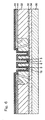
- FIG. 1 A cross-sectional view of a capacitor 1 according to the present embodiment is schematically shown in FIG. 1.
- the capacitor 1 schematically includes a base material 2, a metal layer 3 provided on one main surface of the base material 2, and an extended layer 4 provided on the metal layer 3, a lower electrode layer 6 provided on the surfaces of pores 5 of the base material 2, a dielectric layer 7 provided on the lower electrode layer 6, and an upper electrode layer 8 provided on the dielectric layer 7. Furthermore, the capacitor 1 according to the present embodiment includes: an upper extended electrode 11 provided on the upper electrode layer 8 and a first external electrode 12 provided on the upper extended electrode 11; and a second external electrode 13 electrically insulated from the upper extended electrode 11 and the first external electrode 12 and electrically connected to the base material 2.
- the base material 2 has a pore structure part 16 and a non-pore structure part 17.
- the pore structure part 16 is not conductive, and the non-pore structure part 17 is conductive.
- the pore structure part 16 has a plurality of pores 5 formed, and at least some of the pores 5 penetrate the base material 2.
- One opening of the through-pore is sealed with the metal layer 3.
- the metal layer 3 has a sealing part 18 that seals the opening of the pore 5.
- the sealing part 18 has an oxidized state, but has conductivity.
- the lower electrode layer 6-dielectric layer 7-upper electrode layer 8 constitute an MIM capacitor structure, and charge can be accumulated in the dielectric layer 7 by applying a voltage between the lower electrode layer 6 and the upper electrode layer 8.
- the lower electrode layer 6 is electrically connected to the extended layer 4 through the sealing part 18 of the metal layer 3.
- the extended layer 4 is electrically connected to a non-pore structure part 17 of the base material 2 through the metal layer 3.
- the non-pore structure part 17 of the base material 2 is electrically connected to the second external electrode 13.
- the upper electrode layer 8 is electrically connected to the upper extended electrode 11, and the upper extended electrode 11 is electrically connected to the external electrode 12. More specifically, in the capacitor 1 according to the present embodiment, the current on the side with the lower electrode layer 6 flows through in the order of lower electrode layer 6 - metal layer 3 (specifically sealing part 18) - extended layer 4 - metal layer 3 - non-pore structure part 17 of base material 2 - second external electrode 13 (or vice versa).
- the current may partially flow through in the order of lower electrode layer 6 - metal layer 3 - non-pore structure part 17 of base material 2 - second external electrode 13, without passing through the extended layer 4.
- the current on the side with the upper electrode layer 8 flows through in the order of upper electrode layer 8 - upper extended electrode 11 - external electrode 12 (or vice versa).
- the capacitor 1 as mentioned above is manufactured, for example, as follows.
- a layer 34 corresponding to the extended layer 4 is formed , a barrier layer 33 corresponding to the metal layer 3 is formed thereon, and a base layer 32 corresponding to the base material 2 is further formed thereon (FIG. 2).
- the substrate 30 supports the base layer 32, the barrier layer 33, and the extended layer 34. After the capacitor is manufactured, the substrate 30 supports the base material 2, the metal layer 3, and the extended layer 4. The substrate 30 may be removed after manufacturing the capacitor.
- the substrate 30 is not particularly limited, but a silicon wafer is preferably used.
- the material constituting the extended layer 34 is not particularly limited as long as the material is conductive, and examples thereof include Al, Cu, Ag, Ti, Ta, or alloys thereof such as AlCu, or nitrides TiN and TaN.
- the extended layer 34 may be a single layer, or may be multi-layer, for example, two-layer or three-layer.
- the extended layer 34 is a single layer.
- the extended layer 34 is multi-layer, and can be preferably a three-layer structure of TiN-AlCu-TiN.
- the thickness of the extended layer 34 (the total in the case of a multi-layer) can be, for example, 0.5 ⁇ m or more and 20 ⁇ m or less, preferably 1 ⁇ m or more and 10 ⁇ m or less, more preferably 2 ⁇ m or more and 5 ⁇ m or less.
- the thickness of the layer is adjusted to 0.5 ⁇ m or more, thereby allowing the equivalent series resistance to be reduced.
- the thickness of the layer is increased, thereby allowing the equivalent series resistance to be further reduced.
- the thickness of the layer is adjusted to 20 ⁇ m or less, thereby allowing the capacitor to be further reduced in height.
- the method for forming the extended layer 34 is not particularly limited, and physical vapor deposition (PVD), chemical vapor deposition (CVD), sputtering, plating, and the like can be used.
- PVD physical vapor deposition
- CVD chemical vapor deposition
- sputtering plating, and the like
- plating plating, and the like
- PVD or CVD is used.
- the barrier layer 33 prevents etching from proceeding to the extended layer 4 in a subsequent step, i.e., a step of etching the base layer 32 by anodic oxidation.
- a subsequent step i.e., a step of etching the base layer 32 by anodic oxidation.
- the barrier layer 33 exposed to an etching solution at the bottoms of the through pores is oxidized to serve as the sealing part 18.
- Examples of the material constituting the barrier layer 33 corresponding to the metal layer 3 include Ru, Re, Sn, Ti, V, Fe, Li-Ti alloys, Li-V alloys, or Na-W alloys.
- the thickness of the barrier layer 33 can be, for example, 100 nm or more and 2.0 ⁇ m or less, preferably 150 nm or more and 1.0 ⁇ m or less, more preferably 200 nm or more and 500 nm or less.
- the thickness of the layer is adjusted to 100 nm or more, thereby making it possible to achieve the effect of preventing the etching from proceeding. The effect mentioned above can be further enhanced by increasing the thickness of the layer.
- the thickness of the layer is adjusted to 2.0 ⁇ m or less, the thickness of the sealing part 18 after the capacitor formation is also 2.0 ⁇ m or less, thereby allowing the resistance between the lower electrode layer 6 and the extended layer 4 to be reduced. Reducing the thickness of the layer also reduces the thickness of the sealing part 18 after the capacitor formation, thereby allowing the resistance between the lower electrode layer 6 and the extended layer 4 to be further reduced.
- the method for forming the barrier layer 33 is not particularly limited, and physical vapor deposition (PVD), chemical vapor deposition (CVD), sputtering, plating, and the like can be used.
- PVD physical vapor deposition
- CVD chemical vapor deposition
- sputtering plating, and the like
- plating plating, and the like
- PVD or CVD is used.
- Examples of the material constituting the layer 32 corresponding to the base material 2 include Al, Ti, Nb, Mg, Zn, Fe, W, Zr, or Ta. Preferably, the material is Al.
- the thickness of the base layer 32 can be, for example, 1 ⁇ m or more and 100 ⁇ m or less, preferably 5 ⁇ m or more and 50 ⁇ m or less, more preferably 8 ⁇ m or more and 30 ⁇ m or less.
- the thickness of the layer is adjusted to 1 ⁇ m or more, thereby increasing the depth of pores to be formed later, and then increasing the capacitance of the capacitor obtained.
- the increased thickness of the layer can further increase the capacitance of the capacitor.
- the thickness of the layer is adjusted to 100 ⁇ m or less, thereby allowing the capacitor to be reduced in thickness, and makes it easier to form pores.
- the method for forming the base layer 32 is not particularly limited, and physical vapor deposition (PVD), chemical vapor deposition (CVD), sputtering, plating, and the like can be used.
- PVD physical vapor deposition
- CVD chemical vapor deposition
- sputtering plating, and the like
- plating plating, and the like
- PVD or CVD is used.
- the material constituting the mask 44 corresponding to a part of the insulating part 14 is not particularly limited as long as the material is resistant to an etching agent for use in the subsequent etching step, and examples of the material include SiO 2 , SiN, or SiON. Preferably, the material is SiO 2 .
- the thickness of the mask 44 can be, for example, 0.1 ⁇ m or more and 10 ⁇ m or less, preferably 0.5 ⁇ m or more and 5 ⁇ m or less, for example, 1 ⁇ m or more and 3 ⁇ m or less.
- the thickness of the layer is adjusted to 0.1 ⁇ m or more, thereby allowing the base layer 32 in the mask part to be prevented from being etched.
- the thickness of the mask 44 is further increased, thereby allowing the etching to be prevented more reliably from proceeding, and allowing the insulation property to be further improved.
- the thickness of the mask 44 is adjusted to 10 ⁇ m or less, thereby allowing the capacitor to be further reduced in thickness.
- the method for forming the mask 44 is not particularly limited, and examples of the method include a vacuum vapor deposition method, a chemical vapor deposition method, a sputtering method, an atomic layer deposition (ALD), and a pulsed laser deposition method (PLD).
- the mask can be obtained by forming a mask layer on the entire base layer 32 and then removing, by etching or the like, the mask layer on the part where the pore structure part 16 is to be formed.
- the mask 44 may be formed selectively at a site to be protected.
- the base layer 32 is etched by anodic oxidation to form the pore structure part 16 in the base layer 32 (FIG. 4).
- the conditions for the anodic oxidation treatment such as the etching solution, the temperature, the time, the current density, and the voltage, for example, can be selected depending on the material of the base layer 32, the desired pore structure, and the like.
- the etching solution is an etching solution that is capable of etching the base layer 32, but does not etch the barrier layer 33.
- an etching solution for example, an oxalic acid, a phosphoric acid, a sulfuric acid, a chromic acid, or the like can be used.
- the etching solution is preferably an oxalic acid.
- a preferred combination of the etching solution, the material constituting the base layer 32, and the material constituting the barrier layer 33 is that: the etching solution is an oxalic acid; the material constituting the base layer 32 is Al; and the material constituting the barrier layer 33 is Ru.
- the etching step anodically oxidizes a part of the base layer 32 to form the pore structure part 16.
- the part which is not anodically oxidized because of the masking serves as the non-pore structure part 17.
- the base layer 32 is an aluminum layer, and after the etching step, the treated part becomes anodized aluminum and constitutes the pore structure part 16.
- the untreated part remains aluminum and constitutes the non-pore structure part 17.
- the base layer 32 serves as the base material 2 composed of the pore structure part 16 and the non-pore structure part 17 after the etching step.
- the pore structure part 16 formed by the etching step has a large number of pores formed. At least some of the pores penetrate the base layer 32 and reach the barrier layer 33. According to a preferred aspect, 80% or more, preferably 90% or more, more preferably 98% or more of the pores penetrate through the base layer 32. According to a preferred embodiment, when the pore structure part 16 is planarly viewed from the main surface where the base layer 32 is started to be etched, in a region of 10 ⁇ m or more inside, preferably 5 ⁇ m or more inside, more preferably 1 ⁇ m or more inside from the boundary between the pore structure part 16 and the non-pore structure part 17, 90% or more, preferably substantially all of the pores penetrate the base layer 32. In this regard, the boundary between the pore structure part 16 and the non-pore structure part 17 refers to the boundary between the region oxidized by the anodic oxidation and the region which is not oxidized.
- the shape of the pore 5 is not particularly limited. According to a preferred embodiment, the pore 5 has a cylindrical shape with an axis in the thickness direction of the base material 2.
- the width of the pore 5 (the diameter in the case of a cylindrical shape) is preferably 5 nm or more and 300 nm or less, more preferably 20 nm or more and 200 nm or less.
- the density of the pores 5 is not particularly limited, but is preferably 1 ⁇ 10 8 pores/cm 2 or more and 1 ⁇ 10 12 pores/cm 2 or less, more preferably 1 ⁇ 10 9 pores/cm 2 or more and 1 ⁇ 10 11 pores/cm 2 or less.
- the barrier layer 33 is not etched even in a case where the layer is exposed to the etching solution in the etching step. More specifically, the barrier layer 33 has the function of keeping the etching from proceeding, and seals one opening of the pore 5 to form the sealing part 18.
- a part of the barrier layer 33 exposed to the etching solution, that is, the sealing part 18 can be oxidized. In a case where the sealing part 18 is not sufficiently oxidized, and is preferably further oxidized, the sealing part 18 may be further oxidized by heating or the like.
- the barrier layer 33 in the capacitor according to the present disclosure is made of a metal with conductivity, even in a case where the layer is oxidized in the etching step. More specifically, both the sealing part 18 and the other part 19 of the barrier layer 33 have conductivity after the etching step.
- the metal constituting the barrier layer 33 include Ru, Re, Sn, Ti, V, Fe, Li-Ti alloys, Li-V alloys, or Na-W alloys, and preferably, examples of respective oxides of the metals includes RuO 2 , ReO 3 , SnO 2 , TiO 2 , V 2 O 3 , Fe 3 O 4 , LiTi 2 O 4 , LiV 2 O 4 , and NaWO 3 .
- the use of the metal mentioned above as the metal constituting the barrier layer 33 ensure, even if the sealing part 18 is present between the lower electrode layer 6 of the capacitor structure to be subsequently formed in the pores 5 and the extended layer 4, the electrical connection between the lower electrode layer 6 and the extended layer 4.
- a material that conducts no electricity when the material is oxidized such as tungsten
- the sealing part 18 has conductivity, and the electrical connection between the lower electrode layer 6 and the extended layer 4 can be thus ensured without removing the sealing part 18. More specifically, the capacitor according to the present disclosure is easy to manufacture.
- a mask 45 is formed which covers a region of the pore structure part 16 where there are pores that do not penetrate the base layer 32 and pores that penetrate the base layer 32 but have pore axes greatly inclined with respect to the thickness direction of the base layer 32 (FIG. 5).
- the pores with the axes greatly inclined preferably refer to pores which are preferably 30° or more, more preferably 20° or more, even more preferably 10° or more inclined with respect to the thickness direction of the base layer 32, preferably . Since the pores that do not penetrate and the pores with the axes inclined have variations in pore depth (length), there is a possibility that the surface area may vary, and thus, the electrical characteristics of the capacitor may vary. Covering such pores with the mask 45 makes it possible to obtain a capacitor with small variations in electrical characteristics.
- the material constituting the mask 45 is not limited as long as the material is resistant to the subsequent layer formation step, typically an atomic layer deposition step, and examples of the material include SiO 2 , SiN, or SiON. Preferably, the material is SiO 2 .
- the mask 45 is made of the same material as the mask 44.
- the mask 44 and the mask 45 are made of the same material, thereby improving the adhesion between both the layers, and allowing the generation of stress between both the layers to be suppressed.
- the mask 44 and the mask 45 are both SiO 2 .
- the thickness of the mask 45 can be, for example, 0.1 ⁇ m or more and 10 ⁇ m or less, preferably 0.5 ⁇ m or more and 5 ⁇ m or less, for example, 1 ⁇ m or more and 3 ⁇ m or less.
- the thickness of the layer is adjusted to 0.1 ⁇ m or more, thereby allowing the base layer 32 in the mask part to be prevented from being etched.
- the thickness of the mask 44 is further increased, thereby allowing the etching to be prevented more reliably from proceeding, and allowing the insulation property to be further improved.
- the thickness of the mask 44 is adjusted to 10 ⁇ m or less, thereby allowing the capacitor to be further reduced in thickness.
- the method for forming the mask 45 is not particularly limited, and examples of the method include a vacuum vapor deposition method, a chemical vapor deposition method, a sputtering method, ALD, and PLD.
- an MIM structure is formed on the base layer 32 (base material 2) including the inside of the pores 5 (FIG. 6).
- the lower electrode layer 6 is formed.
- the material that forms the lower electrode layer 6 mentioned above is not particularly limited as long as the material is conductive, and examples of the material include Ni, Cu, Al, W, Ti, Ag, Au, Pt, Zn, Sn, Pb, Fe, Cr, Mo, Ru, Pd, and Ta and alloys thereof, e.g., CuNi, AuNi, AuSn, and metal oxides and metal oxynitrides such as TiN, TiAlN, TiON, TiAlON, and TaN.
- the thickness of the lower electrode layer 6 is not particularly limited, but is preferably 10 to 50 nm, for example.
- the thickness of the lower electrode layer is increased, for example, to 10 nm or more, allowing the ESR to be further reduced.
- the thickness of the lower electrode layer is decreased, for example, to 50 nm or less, thereby making it possible to form a MIM structure without filling the pores, that is, without reducing the surface area of the base material 2, and allowing high capacitance to be achieved.
- the method for forming the lower electrode layer 6 is not particularly limited, and examples of the method include a vacuum vapor deposition method, a chemical vapor deposition method, a sputtering method, ALD, and PLD.
- the ALD is preferred, because the ALD can form a more homogeneous and denser film even in microscopic regions of the pores.
- the dielectric layer 7 is formed on the lower electrode layer 6.
- the material that forms the dielectric layer 7 mentioned above is not particularly limited as long as the material has an insulating property, but examples thereof preferably include metal oxides such as AlO x (e.g., Al 2 O 3 ), SiO x (e.g., SiO 2 ), AlTiO x , SiTiO x , HfO x , TaO x , ZrO x , HfSiO x , ZrSiO x , TiZrO x , TiZrWO x , TiO x , SrTiO x , PbTiO x , BaTiO x , BaSrTiO x , BaCaTiO x , and SiAlO x ; metal nitrides such as AlN x , SiN x , and AlScN x ; or metal oxynitrides such as AlO x N y , SiO x N
- the formulas mentioned above are merely intended to represent the constitutions of the materials, but not intended to limit the compositions. More specifically, the x, y, and z attached to O and N may have any value larger than 0, and the respective elements including the metal elements may have any presence proportion.
- the thickness of the dielectric layer 7 mentioned above is not particularly limited, but for example, preferably 5 nm or more and 100 nm or less, more preferably 10 nm or more and 50 nm or less.
- the dielectric layer of 5 nm or more in thickness can increase the insulating property, and thus allows leakage current to be reduced.
- the dielectric layer of 100 nm or less in thickness makes it possible to achieve higher electrostatic capacitance.
- the method for forming the dielectric layer 7 is not particularly limited, and examples of the method include a vacuum vapor deposition method, a chemical vapor deposition method, a sputtering method, ALD, and PLD.
- the ALD is preferred, because the ALD can form a more homogeneous and denser film even in microscopic regions of the pores.
- the upper electrode layer 8 is formed on the dielectric layer 7.
- the material constituting the upper electrode layer 8 mentioned above is not particularly limited as long as the material is conductive, and examples of the material include Ni, Cu, Al, W, Ti, Ag, Au, Pt, Zn, Sn, Pb, Fe, Cr, Mo, Ru, Pd, and Ta and alloys thereof, e.g., CuNi, AuNi, AuSn, and metal oxides and metal oxynitrides such as TiN, TiAlN, TiON, TiAlON, and TaN.
- the thickness of the upper electrode layer 8 is not particularly limited, but is preferably 10 to 50 nm, for example.
- the thickness of the lower electrode layer is increased, for example, to 10 nm or more, allowing the ESR to be further reduced.
- the method for forming the lower electrode layer 6 is not particularly limited, and examples of the method include a vacuum vapor deposition method, a chemical vapor deposition method, a sputtering method, ALD, and PLD.
- the ALD is preferred, because the ALD can form a more homogeneous and denser film even in microscopic regions of the pores.
- the upper extended electrode 11 is formed on the upper electrode layer 8 (FIG. 7).
- the material constituting the upper extended electrode 11 mentioned above is not particularly limited as long as the material has a conductive property, but examples of the material include Ni, Cu, Al, W, Ti, Ag, Au, Pt, Zn, Sn, Pb, Fe, Cr, Mo, Ru, Pd, and Ta and alloys thereof, e.g., CuNi, AuNi, AuSn, metal oxides and metal oxynitrides such as TiN, TiAlN, TiON, TiAlON, TaN, and electrically conductive polymers (for example, PEDOT (poly(3,4-ethylenedioxythiophene)), polypyrrole, polyaniline).
- PEDOT poly(3,4-ethylenedioxythiophene)
- polypyrrole polyaniline
- the thickness of the upper extended electrode 11 is not particularly limited, but for example, preferably 3 nm or more, more preferably 10 nm or more.
- the upper extended electrode of 3 nm or more in thickness can reduce the resistance of the upper extended electrode itself.
- the upper extended electrode 11 may be formed so as to fill the inside of the pores 5. The ESR is further reduced by filling the inside of the pores with the upper extended electrode.
- the upper extended electrode 11 may be formed by a method such as a chemical vapor deposition method, a plating method, a bias sputtering method, a Sol-Gel method, conductive polymer filling, or ALD. Moreover, multiple methods may be combined for the formation.
- the materials constituting the first external electrode 12 and second external electrode 13 are not particularly limited, but examples of the materials include metals such as Au, Pb, Ag, Sn, Ni, and Cu, and alloys thereof, and electrically conductive polymers.
- the method for forming the first external electrode 12 and the second external electrode 13 is not particularly limited, but for example, CVD, electrolytic plating, electroless plating, vapor deposition, sputtering, conductive paste baking, and the like can be used, and electrolytic plating, electroless plating, vapor deposition, sputtering, and the like are preferred.
- the capacitor according to the present disclosure is small in size, high in capacitance, and further low in equivalent series resistance, and thus can be used for various applications.
Landscapes
- Engineering & Computer Science (AREA)
- Power Engineering (AREA)
- Microelectronics & Electronic Packaging (AREA)
- Manufacturing & Machinery (AREA)
- Semiconductor Integrated Circuits (AREA)
- Fixed Capacitors And Capacitor Manufacturing Machines (AREA)
Abstract
The present invention provides a capacitor including: a base material including a pore structure part; a metal layer provided on one main surface of the base material; an extended layer provided on the metal layer; a lower electrode layer provided on surfaces of pores in the pore structure part; a dielectric layer provided on the lower electrode layer; and an upper electrode layer provided on the dielectric layer, where at least some of the pores penetrate the base material, the metal layer has a sealing part that seals one opening of a pore that penetrates, and the sealing part is conductive, and the lower electrode layer is electrically connected to the extended layer through the sealing part of the metal layer.
Description
The present invention relates to a capacitor.
In recent years, there is a growing demand for reduction in size and increase in capacitance for capacitors. In response to such a demand, capacitors have been proposed which have a metal-dielectric-metal (hereinafter also referred to as an “MIM”) structure formed on a base material that has a surface area increased by a fine structure such as a porous structure. For example, Patent Document 1 discloses a capacitor that has an MIM structure provided in a nanotube formed in an aluminum base material. The nanotube structure in Patent Document 1, which can be obtained by anodically oxidizing an aluminum base material, has very fine and high-density pores. The capacitor in Patent Document 1 has a capacitance increased by providing the MIM structure in such fine and high-density pores.
[Patent Literature 1] US Pat. No. 8,912,522
As described in Patent Document 1, high capacitance can be ensured by providing a porous structure in the base material and forming a capacitor structure in the pores. In the case of providing a capacitor structure in the pores, however, there is the problem of equivalent series resistance (hereinafter also referred to as “ESR”) increased, because of the thin capacitor electrodes, in particular, because the lower electrode has a relatively long distance to an external electrode.
In order to reduce the ESR of a capacitor with a nanotube structure as in Patent Document 1, it is conceivable to extend the lower electrode from the bottom of the pore, and connect the extended electrode to the external electrode through a conductive layer which is larger in cross-sectional area and is disposed below the base material. In a case where such a structure is to be applied, it is necessary to provide a conductive layer on one main surface of the aluminum base material and perform anodic oxidation from the other main surface, and it is necessary to provide a barrier layer between the aluminum base material and the conductive layer such that the conductive layer is not eroded by the anodic oxidation. It is conceivable to use a tungsten layer as such a barrier layer, but in this case, when a pore is formed by the anodic oxidation to penetrate the aluminum, the tungsten layer exposed to the bottom of the pore can also be oxidized. Since such tungsten oxide has low conductivity, the lower electrode in the pore and the conductive layer are electrically cut off. Accordingly, it becomes necessary to remove the barrier layer at the pore bottom, and the manufacturing process will be complicated. In addition, the barrier layer at the pore bottom can be removed by etching, but in order to remove only this tungsten oxide, it is necessary to select the etching solution and set other conditions.
An object of the present disclosure is to provide a capacitor including a fine pore structure, without requiring the above-mentioned barrier layer removal step.
The present disclosure includes the following aspects:
[1] A capacitor including:
a base material including a pore structure part;
a metal layer provided on one main surface of the base material;
an extended layer provided on the metal layer;
a lower electrode layer provided on surfaces of pores in the pore structure part;
a dielectric layer provided on the lower electrode layer; and
an upper electrode layer provided on the dielectric layer,
where
at least some of the pores penetrate the base material,
the metal layer has a sealing part that seals one opening of a pore that penetrates, and the sealing part is conductive, and
the lower electrode layer is electrically connected to the extended layer through the sealing part of the metal layer.
[2] The capacitor according to the foregoing [1], where the base material is an aluminum base material, and is oxidized in the pore structure part.
[3] The capacitor according to the foregoing [1] or [2], where the metal layer is a layer of Ru, Re, Sn, Ti, V, Fe, a Li-Ti alloy, a Li-V alloy, or a Na-W alloy, and is oxidized in the sealing part.
[4] The capacitor according to any of the foregoing [1] to [3], where the metal layer is 10 nm or more and 1.0 μm or less in thickness.
[1] A capacitor including:
a base material including a pore structure part;
a metal layer provided on one main surface of the base material;
an extended layer provided on the metal layer;
a lower electrode layer provided on surfaces of pores in the pore structure part;
a dielectric layer provided on the lower electrode layer; and
an upper electrode layer provided on the dielectric layer,
where
at least some of the pores penetrate the base material,
the metal layer has a sealing part that seals one opening of a pore that penetrates, and the sealing part is conductive, and
the lower electrode layer is electrically connected to the extended layer through the sealing part of the metal layer.
[2] The capacitor according to the foregoing [1], where the base material is an aluminum base material, and is oxidized in the pore structure part.
[3] The capacitor according to the foregoing [1] or [2], where the metal layer is a layer of Ru, Re, Sn, Ti, V, Fe, a Li-Ti alloy, a Li-V alloy, or a Na-W alloy, and is oxidized in the sealing part.
[4] The capacitor according to any of the foregoing [1] to [3], where the metal layer is 10 nm or more and 1.0 μm or less in thickness.
According to the present disclosure, a capacitor can be provided which is low in equivalent series resistance and easy to manufacture.
A capacitor according to the present disclosure will be described in detail below with reference to the drawings. However, the capacitor according to the present embodiment, and the shapes and arrangement of respective constructional elements are not limited to the examples shown in the figures.
A cross-sectional view of a capacitor 1 according to the present embodiment is schematically shown in FIG. 1.
As shown in FIG. 1, the capacitor 1 according to the present embodiment schematically includes a base material 2, a metal layer 3 provided on one main surface of the base material 2, and an extended layer 4 provided on the metal layer 3, a lower electrode layer 6 provided on the surfaces of pores 5 of the base material 2, a dielectric layer 7 provided on the lower electrode layer 6, and an upper electrode layer 8 provided on the dielectric layer 7. Furthermore, the capacitor 1 according to the present embodiment includes: an upper extended electrode 11 provided on the upper electrode layer 8 and a first external electrode 12 provided on the upper extended electrode 11; and a second external electrode 13 electrically insulated from the upper extended electrode 11 and the first external electrode 12 and electrically connected to the base material 2. The base material 2 has a pore structure part 16 and a non-pore structure part 17. The pore structure part 16 is not conductive, and the non-pore structure part 17 is conductive. The pore structure part 16 has a plurality of pores 5 formed, and at least some of the pores 5 penetrate the base material 2. One opening of the through-pore is sealed with the metal layer 3. The metal layer 3 has a sealing part 18 that seals the opening of the pore 5. The sealing part 18 has an oxidized state, but has conductivity. The lower electrode layer 6-dielectric layer 7-upper electrode layer 8 constitute an MIM capacitor structure, and charge can be accumulated in the dielectric layer 7 by applying a voltage between the lower electrode layer 6 and the upper electrode layer 8. The lower electrode layer 6 is electrically connected to the extended layer 4 through the sealing part 18 of the metal layer 3. The extended layer 4 is electrically connected to a non-pore structure part 17 of the base material 2 through the metal layer 3. The non-pore structure part 17 of the base material 2 is electrically connected to the second external electrode 13. The upper electrode layer 8 is electrically connected to the upper extended electrode 11, and the upper extended electrode 11 is electrically connected to the external electrode 12. More specifically, in the capacitor 1 according to the present embodiment, the current on the side with the lower electrode layer 6 flows through in the order of lower electrode layer 6 - metal layer 3 (specifically sealing part 18) - extended layer 4 - metal layer 3 - non-pore structure part 17 of base material 2 - second external electrode 13 (or vice versa). Further, the current may partially flow through in the order of lower electrode layer 6 - metal layer 3 - non-pore structure part 17 of base material 2 - second external electrode 13, without passing through the extended layer 4. On the other hand, the current on the side with the upper electrode layer 8 flows through in the order of upper electrode layer 8 - upper extended electrode 11 - external electrode 12 (or vice versa).
The capacitor 1 as mentioned above is manufactured, for example, as follows.
(Layer Formation Step)
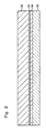
On asubstrate 30, a layer 34 corresponding to the extended layer 4 is formed , a barrier layer 33 corresponding to the metal layer 3 is formed thereon, and a base layer 32 corresponding to the base material 2 is further formed thereon (FIG. 2).
On a
The substrate 30 supports the base layer 32, the barrier layer 33, and the extended layer 34. After the capacitor is manufactured, the substrate 30 supports the base material 2, the metal layer 3, and the extended layer 4. The substrate 30 may be removed after manufacturing the capacitor.
The substrate 30 is not particularly limited, but a silicon wafer is preferably used.
The material constituting the extended layer 34 is not particularly limited as long as the material is conductive, and examples thereof include Al, Cu, Ag, Ti, Ta, or alloys thereof such as AlCu, or nitrides TiN and TaN.
The extended layer 34 may be a single layer, or may be multi-layer, for example, two-layer or three-layer.
According to one aspect, the extended layer 34 is a single layer.
According to another embodiment, the extended layer 34 is multi-layer, and can be preferably a three-layer structure of TiN-AlCu-TiN.
The thickness of the extended layer 34 (the total in the case of a multi-layer) can be, for example, 0.5 μm or more and 20 μm or less, preferably 1 μm or more and 10 μm or less, more preferably 2 μm or more and 5 μm or less. The thickness of the layer is adjusted to 0.5 μm or more, thereby allowing the equivalent series resistance to be reduced. The thickness of the layer is increased, thereby allowing the equivalent series resistance to be further reduced. On the other hand, the thickness of the layer is adjusted to 20 μm or less, thereby allowing the capacitor to be further reduced in height.
The method for forming the extended layer 34 is not particularly limited, and physical vapor deposition (PVD), chemical vapor deposition (CVD), sputtering, plating, and the like can be used. Preferably, PVD or CVD is used.
The barrier layer 33 prevents etching from proceeding to the extended layer 4 in a subsequent step, i.e., a step of etching the base layer 32 by anodic oxidation. In this regard, the barrier layer 33 exposed to an etching solution at the bottoms of the through pores is oxidized to serve as the sealing part 18.
Examples of the material constituting the barrier layer 33 corresponding to the metal layer 3 include Ru, Re, Sn, Ti, V, Fe, Li-Ti alloys, Li-V alloys, or Na-W alloys.
The thickness of the barrier layer 33 can be, for example, 100 nm or more and 2.0 μm or less, preferably 150 nm or more and 1.0 μm or less, more preferably 200 nm or more and 500 nm or less. The thickness of the layer is adjusted to 100 nm or more, thereby making it possible to achieve the effect of preventing the etching from proceeding. The effect mentioned above can be further enhanced by increasing the thickness of the layer. On the other hand, when the thickness of the layer is adjusted to 2.0 μm or less, the thickness of the sealing part 18 after the capacitor formation is also 2.0 μm or less, thereby allowing the resistance between the lower electrode layer 6 and the extended layer 4 to be reduced. Reducing the thickness of the layer also reduces the thickness of the sealing part 18 after the capacitor formation, thereby allowing the resistance between the lower electrode layer 6 and the extended layer 4 to be further reduced.
The method for forming the barrier layer 33 is not particularly limited, and physical vapor deposition (PVD), chemical vapor deposition (CVD), sputtering, plating, and the like can be used. Preferably, PVD or CVD is used.
Examples of the material constituting the layer 32 corresponding to the base material 2 include Al, Ti, Nb, Mg, Zn, Fe, W, Zr, or Ta. Preferably, the material is Al.
The thickness of the base layer 32 can be, for example, 1 μm or more and 100 μm or less, preferably 5 μm or more and 50 μm or less, more preferably 8 μm or more and 30 μm or less. The thickness of the layer is adjusted to 1 μm or more, thereby increasing the depth of pores to be formed later, and then increasing the capacitance of the capacitor obtained. The increased thickness of the layer can further increase the capacitance of the capacitor. On the other hand, the thickness of the layer is adjusted to 100 μm or less, thereby allowing the capacitor to be reduced in thickness, and makes it easier to form pores.
The method for forming the base layer 32 is not particularly limited, and physical vapor deposition (PVD), chemical vapor deposition (CVD), sputtering, plating, and the like can be used. Preferably, PVD or CVD is used.
(Etching Step)
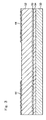
First, amask 44 corresponding to a part an insulating part 14 is formed on the base layer 32, except for a part where the pore structure part 16 is formed (FIG. 3).
First, a
The material constituting the mask 44 corresponding to a part of the insulating part 14 is not particularly limited as long as the material is resistant to an etching agent for use in the subsequent etching step, and examples of the material include SiO2, SiN, or SiON. Preferably, the material is SiO2.
The thickness of the mask 44 can be, for example, 0.1 μm or more and 10 μm or less, preferably 0.5 μm or more and 5 μm or less, for example, 1 μm or more and 3 μm or less. The thickness of the layer is adjusted to 0.1 μm or more, thereby allowing the base layer 32 in the mask part to be prevented from being etched. In addition, it is possible to improve the insulation property between the non-pore structure part 17 of the base material 2 and the lower electrode layer 6 on the insulating part 14 after the capacitor formation. The thickness of the mask 44 is further increased, thereby allowing the etching to be prevented more reliably from proceeding, and allowing the insulation property to be further improved. On the other hand, the thickness of the mask 44 is adjusted to 10 μm or less, thereby allowing the capacitor to be further reduced in thickness.
The method for forming the mask 44 is not particularly limited, and examples of the method include a vacuum vapor deposition method, a chemical vapor deposition method, a sputtering method, an atomic layer deposition (ALD), and a pulsed laser deposition method (PLD). For example, the mask can be obtained by forming a mask layer on the entire base layer 32 and then removing, by etching or the like, the mask layer on the part where the pore structure part 16 is to be formed. As an alternative method, the mask 44 may be formed selectively at a site to be protected.
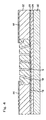
Next, the base layer 32 is etched by anodic oxidation to form the pore structure part 16 in the base layer 32 (FIG. 4).
The conditions for the anodic oxidation treatment, such as the etching solution, the temperature, the time, the current density, and the voltage, for example, can be selected depending on the material of the base layer 32, the desired pore structure, and the like.
The etching solution is an etching solution that is capable of etching the base layer 32, but does not etch the barrier layer 33. As such an etching solution, for example, an oxalic acid, a phosphoric acid, a sulfuric acid, a chromic acid, or the like can be used. The etching solution is preferably an oxalic acid.
A preferred combination of the etching solution, the material constituting the base layer 32, and the material constituting the barrier layer 33 is that: the etching solution is an oxalic acid; the material constituting the base layer 32 is Al; and the material constituting the barrier layer 33 is Ru.
The etching step anodically oxidizes a part of the base layer 32 to form the pore structure part 16. The part which is not anodically oxidized because of the masking serves as the non-pore structure part 17.
According to one aspect, the base layer 32 is an aluminum layer, and after the etching step, the treated part becomes anodized aluminum and constitutes the pore structure part 16. The untreated part remains aluminum and constitutes the non-pore structure part 17. More specifically, the base layer 32 serves as the base material 2 composed of the pore structure part 16 and the non-pore structure part 17 after the etching step.
The pore structure part 16 formed by the etching step has a large number of pores formed. At least some of the pores penetrate the base layer 32 and reach the barrier layer 33. According to a preferred aspect, 80% or more, preferably 90% or more, more preferably 98% or more of the pores penetrate through the base layer 32. According to a preferred embodiment, when the pore structure part 16 is planarly viewed from the main surface where the base layer 32 is started to be etched, in a region of 10 μm or more inside, preferably 5 μm or more inside, more preferably 1 μm or more inside from the boundary between the pore structure part 16 and the non-pore structure part 17, 90% or more, preferably substantially all of the pores penetrate the base layer 32. In this regard, the boundary between the pore structure part 16 and the non-pore structure part 17 refers to the boundary between the region oxidized by the anodic oxidation and the region which is not oxidized.
The shape of the pore 5 is not particularly limited. According to a preferred embodiment, the pore 5 has a cylindrical shape with an axis in the thickness direction of the base material 2.
The width of the pore 5 (the diameter in the case of a cylindrical shape) is preferably 5 nm or more and 300 nm or less, more preferably 20 nm or more and 200 nm or less.
The density of the pores 5 is not particularly limited, but is preferably 1 × 10⁸ pores/cm2 or more and 1 × 10¹² pores/cm2 or less, more preferably 1 × 10⁹ pores/cm2 or more and 1 × 10¹¹ pores/cm2 or less.
The barrier layer 33 is not etched even in a case where the layer is exposed to the etching solution in the etching step. More specifically, the barrier layer 33 has the function of keeping the etching from proceeding, and seals one opening of the pore 5 to form the sealing part 18. A part of the barrier layer 33 exposed to the etching solution, that is, the sealing part 18 can be oxidized. In a case where the sealing part 18 is not sufficiently oxidized, and is preferably further oxidized, the sealing part 18 may be further oxidized by heating or the like.
The barrier layer 33 in the capacitor according to the present disclosure is made of a metal with conductivity, even in a case where the layer is oxidized in the etching step. More specifically, both the sealing part 18 and the other part 19 of the barrier layer 33 have conductivity after the etching step. As mentioned above, examples of the metal constituting the barrier layer 33 include Ru, Re, Sn, Ti, V, Fe, Li-Ti alloys, Li-V alloys, or Na-W alloys, and preferably, examples of respective oxides of the metals includes RuO2, ReO3, SnO2, TiO2, V2O3, Fe3O4, LiTi2O4, LiV2O4, and NaWO3.
The use of the metal mentioned above as the metal constituting the barrier layer 33 ensure, even if the sealing part 18 is present between the lower electrode layer 6 of the capacitor structure to be subsequently formed in the pores 5 and the extended layer 4, the electrical connection between the lower electrode layer 6 and the extended layer 4. On the other hand, in a case where a material that conducts no electricity when the material is oxidized, such as tungsten, is used for the barrier layer 33, it is necessary to remove the sealing part 18 present between the lower electrode layer 6 and the extended layer 4 in order to ensure the electrical connection between the lower electrode layer 6 and the extended layer 4. In this case, the sealing part 18 has to be removed without affecting the base material 2, and an extremely difficult treatment is required. On the other hand, in the capacitor according to the present disclosure, the sealing part 18 has conductivity, and the electrical connection between the lower electrode layer 6 and the extended layer 4 can be thus ensured without removing the sealing part 18. More specifically, the capacitor according to the present disclosure is easy to manufacture.
(Capacitor Structure Formation Step)
Next, the MIM capacitor structure of lower electrode layer 6 - dielectric layer 7 -upper electrode layer 8 is formed.
Next, the MIM capacitor structure of lower electrode layer 6 - dielectric layer 7 -
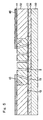
First, a mask 45 is formed which covers a region of the pore structure part 16 where there are pores that do not penetrate the base layer 32 and pores that penetrate the base layer 32 but have pore axes greatly inclined with respect to the thickness direction of the base layer 32 (FIG. 5). In this regard, the pores with the axes greatly inclined preferably refer to pores which are preferably 30° or more, more preferably 20° or more, even more preferably 10° or more inclined with respect to the thickness direction of the base layer 32, preferably . Since the pores that do not penetrate and the pores with the axes inclined have variations in pore depth (length), there is a possibility that the surface area may vary, and thus, the electrical characteristics of the capacitor may vary. Covering such pores with the mask 45 makes it possible to obtain a capacitor with small variations in electrical characteristics.
The material constituting the mask 45 is not limited as long as the material is resistant to the subsequent layer formation step, typically an atomic layer deposition step, and examples of the material include SiO2, SiN, or SiON. Preferably, the material is SiO2.
According to one embodiment, the mask 45 is made of the same material as the mask 44. The mask 44 and the mask 45 are made of the same material, thereby improving the adhesion between both the layers, and allowing the generation of stress between both the layers to be suppressed. According to a preferred aspect, since SiO2 has resistance to both the etching step and the ALD step, the mask 44 and the mask 45 are both SiO2.
The thickness of the mask 45 can be, for example, 0.1 μm or more and 10 μm or less, preferably 0.5 μm or more and 5 μm or less, for example, 1 μm or more and 3 μm or less. The thickness of the layer is adjusted to 0.1 μm or more, thereby allowing the base layer 32 in the mask part to be prevented from being etched. In addition, it is possible to improve the insulation property between the non-pore structure part 17 of the base material 2 and the lower electrode layer 6 on the insulating part 14 after the capacitor formation. The thickness of the mask 44 is further increased, thereby allowing the etching to be prevented more reliably from proceeding, and allowing the insulation property to be further improved. On the other hand, the thickness of the mask 44 is adjusted to 10 μm or less, thereby allowing the capacitor to be further reduced in thickness.
The method for forming the mask 45 is not particularly limited, and examples of the method include a vacuum vapor deposition method, a chemical vapor deposition method, a sputtering method, ALD, and PLD.
Next, an MIM structure is formed on the base layer 32 (base material 2) including the inside of the pores 5 (FIG. 6).
First, the lower electrode layer 6 is formed.
The material that forms the lower electrode layer 6 mentioned above is not particularly limited as long as the material is conductive, and examples of the material include Ni, Cu, Al, W, Ti, Ag, Au, Pt, Zn, Sn, Pb, Fe, Cr, Mo, Ru, Pd, and Ta and alloys thereof, e.g., CuNi, AuNi, AuSn, and metal oxides and metal oxynitrides such as TiN, TiAlN, TiON, TiAlON, and TaN.
The thickness of the lower electrode layer 6 is not particularly limited, but is preferably 10 to 50 nm, for example. The thickness of the lower electrode layer is increased, for example, to 10 nm or more, allowing the ESR to be further reduced. In addition, the thickness of the lower electrode layer is decreased, for example, to 50 nm or less, thereby making it possible to form a MIM structure without filling the pores, that is, without reducing the surface area of the base material 2, and allowing high capacitance to be achieved.
The method for forming the lower electrode layer 6 is not particularly limited, and examples of the method include a vacuum vapor deposition method, a chemical vapor deposition method, a sputtering method, ALD, and PLD. The ALD is preferred, because the ALD can form a more homogeneous and denser film even in microscopic regions of the pores.
Next, the dielectric layer 7 is formed on the lower electrode layer 6.
The material that forms the dielectric layer 7 mentioned above is not particularly limited as long as the material has an insulating property, but examples thereof preferably include metal oxides such as AlOx (e.g., Al2O3), SiOx (e.g., SiO2), AlTiOx, SiTiOx, HfOx, TaOx, ZrOx, HfSiOx, ZrSiOx, TiZrOx, TiZrWOx, TiOx, SrTiOx, PbTiOx, BaTiOx, BaSrTiOx, BaCaTiOx, and SiAlOx; metal nitrides such as AlNx, SiNx, and AlScNx; or metal oxynitrides such as AlOxNy, SiOxNy, HfSiOxNy, and SiCxOyNz, and AlOx, SiOx, SiOxNy, and HfSiOx are preferred. It is to be noted that the formulas mentioned above are merely intended to represent the constitutions of the materials, but not intended to limit the compositions. More specifically, the x, y, and z attached to O and N may have any value larger than 0, and the respective elements including the metal elements may have any presence proportion.
The thickness of the dielectric layer 7 mentioned above is not particularly limited, but for example, preferably 5 nm or more and 100 nm or less, more preferably 10 nm or more and 50 nm or less. The dielectric layer of 5 nm or more in thickness can increase the insulating property, and thus allows leakage current to be reduced. In addition, the dielectric layer of 100 nm or less in thickness makes it possible to achieve higher electrostatic capacitance.
The method for forming the dielectric layer 7 is not particularly limited, and examples of the method include a vacuum vapor deposition method, a chemical vapor deposition method, a sputtering method, ALD, and PLD. The ALD is preferred, because the ALD can form a more homogeneous and denser film even in microscopic regions of the pores.
Next, the upper electrode layer 8 is formed on the dielectric layer 7.
The material constituting the upper electrode layer 8 mentioned above is not particularly limited as long as the material is conductive, and examples of the material include Ni, Cu, Al, W, Ti, Ag, Au, Pt, Zn, Sn, Pb, Fe, Cr, Mo, Ru, Pd, and Ta and alloys thereof, e.g., CuNi, AuNi, AuSn, and metal oxides and metal oxynitrides such as TiN, TiAlN, TiON, TiAlON, and TaN.
The thickness of the upper electrode layer 8 is not particularly limited, but is preferably 10 to 50 nm, for example. The thickness of the lower electrode layer is increased, for example, to 10 nm or more, allowing the ESR to be further reduced.
The method for forming the lower electrode layer 6 is not particularly limited, and examples of the method include a vacuum vapor deposition method, a chemical vapor deposition method, a sputtering method, ALD, and PLD. The ALD is preferred, because the ALD can form a more homogeneous and denser film even in microscopic regions of the pores.
(External Electrode Formation Step)
Next, the external electrodes 12 and 13 are formed.
Next, the
First, the upper extended electrode 11 is formed on the upper electrode layer 8 (FIG. 7).
The material constituting the upper extended electrode 11 mentioned above is not particularly limited as long as the material has a conductive property, but examples of the material include Ni, Cu, Al, W, Ti, Ag, Au, Pt, Zn, Sn, Pb, Fe, Cr, Mo, Ru, Pd, and Ta and alloys thereof, e.g., CuNi, AuNi, AuSn, metal oxides and metal oxynitrides such as TiN, TiAlN, TiON, TiAlON, TaN, and electrically conductive polymers (for example, PEDOT (poly(3,4-ethylenedioxythiophene)), polypyrrole, polyaniline).
The thickness of the upper extended electrode 11 is not particularly limited, but for example, preferably 3 nm or more, more preferably 10 nm or more. The upper extended electrode of 3 nm or more in thickness can reduce the resistance of the upper extended electrode itself. In addition, the upper extended electrode 11 may be formed so as to fill the inside of the pores 5. The ESR is further reduced by filling the inside of the pores with the upper extended electrode.
The upper extended electrode 11 may be formed by a method such as a chemical vapor deposition method, a plating method, a bias sputtering method, a Sol-Gel method, conductive polymer filling, or ALD. Moreover, multiple methods may be combined for the formation.
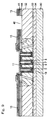
Then, the surface a part of the base layer 32 electrically connected to the lower electrode layer 6 is partially exposed (FIG. 8), and the second external electrode 13 and first external electrode 12 are formed respectively on the exposed part 46 and the upper extended electrode 11 (FIG. 9).
The materials constituting the first external electrode 12 and second external electrode 13 are not particularly limited, but examples of the materials include metals such as Au, Pb, Ag, Sn, Ni, and Cu, and alloys thereof, and electrically conductive polymers.
The method for forming the first external electrode 12 and the second external electrode 13 is not particularly limited, but for example, CVD, electrolytic plating, electroless plating, vapor deposition, sputtering, conductive paste baking, and the like can be used, and electrolytic plating, electroless plating, vapor deposition, sputtering, and the like are preferred.
While the capacitor 1 according to the present embodiment has been described above, various modifications can be made to the capacitor according to the present disclosure.
The capacitor according to the present disclosure is small in size, high in capacitance, and further low in equivalent series resistance, and thus can be used for various applications.
1 capacitor
2 base material
3 metal layer
4 extended layer
5 pore
6 lower electrode layer
7 dielectric layer
8 upper electrode layer
11 upper extended electrode
12 first external electrode
13 second external electrode
16 pore structure part
17 non-pore structure part
18 sealing part
19 other part
30 substrate
32 base layer
33 barrier layer
34 extended layer
44 mask
45 mask
2 base material
3 metal layer
4 extended layer
5 pore
6 lower electrode layer
7 dielectric layer
8 upper electrode layer
11 upper extended electrode
12 first external electrode
13 second external electrode
16 pore structure part
17 non-pore structure part
18 sealing part
19 other part
30 substrate
32 base layer
33 barrier layer
34 extended layer
44 mask
45 mask
Claims (4)
- A capacitor comprising:
a base material comprising a pore structure part;
a metal layer provided on one main surface of the base material;
an extended layer provided on the metal layer;
a lower electrode layer provided on surfaces of pores in the pore structure part;
a dielectric layer provided on the lower electrode layer; and
an upper electrode layer provided on the dielectric layer,
wherein
at least some of the pores penetrate the base material,
the metal layer has a sealing part that seals one opening of a pore that penetrates, and the sealing part is conductive, and
the lower electrode layer is electrically connected to the extended layer through the sealing part of the metal layer. - The capacitor according to claim 1, wherein the base material is an aluminum base material, and is oxidized in the pore structure part.
- The capacitor according to claim 1 or 2, wherein the metal layer is a layer of Ru, Re, Sn, Ti, V, Fe, a Li-Ti alloy, a Li-V alloy, or a Na-W alloy, and is oxidized in the sealing part.
- The capacitor according to any one of claims 1 to 3, wherein the metal layer is 10 nm or more and 1.0 μm or less in thickness.
Applications Claiming Priority (2)
| Application Number | Priority Date | Filing Date | Title |
|---|---|---|---|
| JP2019-017818 | 2019-02-04 | ||
| JP2019017818 | 2019-02-04 |
Publications (1)
| Publication Number | Publication Date |
|---|---|
| WO2020162459A1 true WO2020162459A1 (en) | 2020-08-13 |
Family
ID=69724024
Family Applications (1)
| Application Number | Title | Priority Date | Filing Date |
|---|---|---|---|
| PCT/JP2020/004147 Ceased WO2020162459A1 (en) | 2019-02-04 | 2020-02-04 | Capacitor |
Country Status (1)
| Country | Link |
|---|---|
| WO (1) | WO2020162459A1 (en) |
Cited By (3)
| Publication number | Priority date | Publication date | Assignee | Title |
|---|---|---|---|---|
| EP4060697A1 (en) * | 2021-03-18 | 2022-09-21 | Commissariat à l'énergie atomique et aux énergies alternatives | High-density capacitive device and method for manufacturing such a device |
| US20230138497A1 (en) * | 2021-11-02 | 2023-05-04 | Murata Manufacturing Co., Ltd. | Nanowire array structures for integration, products incorporating the structures, and methods of manufacture thereof |
| EP4194591A1 (en) * | 2021-12-13 | 2023-06-14 | Murata Manufacturing Co., Ltd. | A method for manufacturing an electrical device with an anodic porous oxide region delimited by planarizing a stack of materials |
Citations (3)
| Publication number | Priority date | Publication date | Assignee | Title |
|---|---|---|---|---|
| US8912522B2 (en) | 2009-08-26 | 2014-12-16 | University Of Maryland | Nanodevice arrays for electrical energy storage, capture and management and method for their formation |
| US20160268144A1 (en) * | 2013-10-29 | 2016-09-15 | Ipdia | Structure with an improved capacitor |
| CN105761943B (en) * | 2016-04-14 | 2018-07-10 | 上海大学 | Nickeltin nanohole array and preparation method thereof |
-
2020
- 2020-02-04 WO PCT/JP2020/004147 patent/WO2020162459A1/en not_active Ceased
Patent Citations (3)
| Publication number | Priority date | Publication date | Assignee | Title |
|---|---|---|---|---|
| US8912522B2 (en) | 2009-08-26 | 2014-12-16 | University Of Maryland | Nanodevice arrays for electrical energy storage, capture and management and method for their formation |
| US20160268144A1 (en) * | 2013-10-29 | 2016-09-15 | Ipdia | Structure with an improved capacitor |
| CN105761943B (en) * | 2016-04-14 | 2018-07-10 | 上海大学 | Nickeltin nanohole array and preparation method thereof |
Non-Patent Citations (2)
| Title |
|---|
| CHI-TSUNG HONG ET AL: "Nanotexture Electrode on Nanoporous AAO Dielectric for Micro Tactile Sensing Devices", MICRO ELECTRO MECHANICAL SYSTEMS, 2009. MEMS 2009. IEEE 22ND INTERNATIONAL CONFERENCE ON, IEEE, PISCATAWAY, NJ, USA, 25 January 2009 (2009-01-25), pages 100 - 103, XP031444240, ISBN: 978-1-4244-2977-6 * |
| HOURDAKIS E ET AL: "High-Density MIM Capacitors With Porous Anodic Alumina Dielectric", IEEE TRANSACTIONS ON ELECTRON DEVICES, IEEE SERVICE CENTER, PISACATAWAY, NJ, US, vol. 30, no. 10, 1 October 2010 (2010-10-01), pages 2679 - 2683, XP011316023, ISSN: 0018-9383 * |
Cited By (5)
| Publication number | Priority date | Publication date | Assignee | Title |
|---|---|---|---|---|
| EP4060697A1 (en) * | 2021-03-18 | 2022-09-21 | Commissariat à l'énergie atomique et aux énergies alternatives | High-density capacitive device and method for manufacturing such a device |
| FR3120982A1 (en) * | 2021-03-18 | 2022-09-23 | Commissariat A L'energie Atomique Et Aux Energies Alternatives | HIGH DENSITY CAPACITIVE DEVICE AND METHOD FOR FABRICATING SUCH A DEVICE |
| US12476051B2 (en) | 2021-03-18 | 2025-11-18 | Commissariat à l'énergie atomique et aux énergies alternatives | High-density capacitive device and method for manufacturing such a device |
| US20230138497A1 (en) * | 2021-11-02 | 2023-05-04 | Murata Manufacturing Co., Ltd. | Nanowire array structures for integration, products incorporating the structures, and methods of manufacture thereof |
| EP4194591A1 (en) * | 2021-12-13 | 2023-06-14 | Murata Manufacturing Co., Ltd. | A method for manufacturing an electrical device with an anodic porous oxide region delimited by planarizing a stack of materials |
Similar Documents
| Publication | Publication Date | Title |
|---|---|---|
| US8023249B2 (en) | Capacitor and method of manufacturing the same | |
| JP6102376B2 (en) | Thin film capacitor | |
| US10497582B2 (en) | Capacitor formed in insulated pores of an anodized metal layer | |
| US10256045B2 (en) | Capacitor | |
| TWI646564B (en) | Capacitor | |
| JP5416840B2 (en) | Capacitor and manufacturing method thereof | |
| WO2006014753A1 (en) | Capacitors with high energy storage density and low esr | |
| JP5012996B2 (en) | Capacitor and manufacturing method thereof | |
| US11978766B2 (en) | Three-dimensional capacitive structures and their manufacturing methods | |
| WO2011132492A1 (en) | Thin film capacitor | |
| WO2018092722A1 (en) | Capacitor and capacitor mounting structure | |
| US20180174760A1 (en) | Capacitor | |
| JP7727954B2 (en) | capacitor | |
| US20180114647A1 (en) | Capacitor and method for manufacturing the capacitor | |
| US20050056939A1 (en) | Thin-film capacitor and method of producing the capacitor | |
| US11114242B2 (en) | Capacitor having an oxide film on a surface of a conductive metal base material | |
| US10074478B2 (en) | Capacitor | |
| CN111989426A (en) | Semiconductor device having porous region embedded structure and method of manufacturing the same | |
| JP2019071336A (en) | Thin film capacitor and manufacturing method thereof | |
| US20170040113A1 (en) | Capacitor |
Legal Events
| Date | Code | Title | Description |
|---|---|---|---|
| 121 | Ep: the epo has been informed by wipo that ep was designated in this application |
Ref document number: 20707845 Country of ref document: EP Kind code of ref document: A1 |
|
| NENP | Non-entry into the national phase |
Ref country code: DE |
|
| NENP | Non-entry into the national phase |
Ref country code: JP |
|
| 122 | Ep: pct application non-entry in european phase |
Ref document number: 20707845 Country of ref document: EP Kind code of ref document: A1 |