WO2020158868A1 - 配線板 - Google Patents
配線板 Download PDFInfo
- Publication number
- WO2020158868A1 WO2020158868A1 PCT/JP2020/003447 JP2020003447W WO2020158868A1 WO 2020158868 A1 WO2020158868 A1 WO 2020158868A1 JP 2020003447 W JP2020003447 W JP 2020003447W WO 2020158868 A1 WO2020158868 A1 WO 2020158868A1
- Authority
- WO
- WIPO (PCT)
- Prior art keywords
- dielectric
- wiring board
- board according
- ghz
- ptfe
- Prior art date
- Legal status (The legal status is an assumption and is not a legal conclusion. Google has not performed a legal analysis and makes no representation as to the accuracy of the status listed.)
- Ceased
Links
Images


Classifications
-
- H—ELECTRICITY
- H01—ELECTRIC ELEMENTS
- H01P—WAVEGUIDES; RESONATORS, LINES, OR OTHER DEVICES OF THE WAVEGUIDE TYPE
- H01P11/00—Apparatus or processes specially adapted for manufacturing waveguides or resonators, lines, or other devices of the waveguide type
- H01P11/001—Manufacturing waveguides or transmission lines of the waveguide type
- H01P11/006—Manufacturing dielectric waveguides
-
- C—CHEMISTRY; METALLURGY
- C08—ORGANIC MACROMOLECULAR COMPOUNDS; THEIR PREPARATION OR CHEMICAL WORKING-UP; COMPOSITIONS BASED THEREON
- C08J—WORKING-UP; GENERAL PROCESSES OF COMPOUNDING; AFTER-TREATMENT NOT COVERED BY SUBCLASSES C08B, C08C, C08F, C08G or C08H
- C08J7/00—Chemical treatment or coating of shaped articles made of macromolecular substances
- C08J7/04—Coating
- C08J7/0427—Coating with only one layer of a composition containing a polymer binder
-
- H—ELECTRICITY
- H01—ELECTRIC ELEMENTS
- H01P—WAVEGUIDES; RESONATORS, LINES, OR OTHER DEVICES OF THE WAVEGUIDE TYPE
- H01P3/00—Waveguides; Transmission lines of the waveguide type
-
- H—ELECTRICITY
- H01—ELECTRIC ELEMENTS
- H01P—WAVEGUIDES; RESONATORS, LINES, OR OTHER DEVICES OF THE WAVEGUIDE TYPE
- H01P3/00—Waveguides; Transmission lines of the waveguide type
- H01P3/02—Waveguides; Transmission lines of the waveguide type with two longitudinal conductors
- H01P3/08—Microstrips; Strip lines
- H01P3/081—Microstriplines
-
- H—ELECTRICITY
- H01—ELECTRIC ELEMENTS
- H01P—WAVEGUIDES; RESONATORS, LINES, OR OTHER DEVICES OF THE WAVEGUIDE TYPE
- H01P3/00—Waveguides; Transmission lines of the waveguide type
- H01P3/10—Wire waveguides, i.e. with a single solid longitudinal conductor
-
- H—ELECTRICITY
- H01—ELECTRIC ELEMENTS
- H01P—WAVEGUIDES; RESONATORS, LINES, OR OTHER DEVICES OF THE WAVEGUIDE TYPE
- H01P3/00—Waveguides; Transmission lines of the waveguide type
- H01P3/16—Dielectric waveguides, i.e. without a longitudinal conductor
-
- C—CHEMISTRY; METALLURGY
- C08—ORGANIC MACROMOLECULAR COMPOUNDS; THEIR PREPARATION OR CHEMICAL WORKING-UP; COMPOSITIONS BASED THEREON
- C08J—WORKING-UP; GENERAL PROCESSES OF COMPOUNDING; AFTER-TREATMENT NOT COVERED BY SUBCLASSES C08B, C08C, C08F, C08G or C08H
- C08J2327/00—Characterised by the use of homopolymers or copolymers of compounds having one or more unsaturated aliphatic radicals, each having only one carbon-to-carbon double bond, and at least one being terminated by a halogen; Derivatives of such polymers
- C08J2327/02—Characterised by the use of homopolymers or copolymers of compounds having one or more unsaturated aliphatic radicals, each having only one carbon-to-carbon double bond, and at least one being terminated by a halogen; Derivatives of such polymers not modified by chemical after-treatment
- C08J2327/12—Characterised by the use of homopolymers or copolymers of compounds having one or more unsaturated aliphatic radicals, each having only one carbon-to-carbon double bond, and at least one being terminated by a halogen; Derivatives of such polymers not modified by chemical after-treatment containing fluorine atoms
- C08J2327/18—Homopolymers or copolymers of tetrafluoroethylene
-
- C—CHEMISTRY; METALLURGY
- C08—ORGANIC MACROMOLECULAR COMPOUNDS; THEIR PREPARATION OR CHEMICAL WORKING-UP; COMPOSITIONS BASED THEREON
- C08J—WORKING-UP; GENERAL PROCESSES OF COMPOUNDING; AFTER-TREATMENT NOT COVERED BY SUBCLASSES C08B, C08C, C08F, C08G or C08H
- C08J2427/00—Characterised by the use of homopolymers or copolymers of compounds having one or more unsaturated aliphatic radicals, each having only one carbon-to-carbon double bond, and at least one being terminated by a halogen; Derivatives of such polymers
- C08J2427/02—Characterised by the use of homopolymers or copolymers of compounds having one or more unsaturated aliphatic radicals, each having only one carbon-to-carbon double bond, and at least one being terminated by a halogen; Derivatives of such polymers not modified by chemical after-treatment
- C08J2427/12—Characterised by the use of homopolymers or copolymers of compounds having one or more unsaturated aliphatic radicals, each having only one carbon-to-carbon double bond, and at least one being terminated by a halogen; Derivatives of such polymers not modified by chemical after-treatment containing fluorine atoms
- C08J2427/18—Homopolymers or copolymers of tetrafluoroethylene
Definitions
- the present disclosure relates to wiring boards.
- metal waveguides have been used as transmission lines for transmitting high-frequency signals of microwaves and millimeter waves, but due to the recent demand for miniaturization of high-frequency modules, use of dielectric lines as waveguides. Is being considered.
- Patent Document 1 discloses a dielectric line coupling device including a first conductor plate, a second conductor plate, at least one dielectric strip line, and a dielectric slab, wherein the first conductor plate is provided. And the second conductor plate is arranged so as to be spaced from each other and to face each other, and the dielectric strip line is arranged between the first conductor plate and the second conductor plate.
- the dielectric slab is made of a dielectric thin plate and is in surface contact with one of the side surfaces of the first and second conductor plates, and the end portion is in contact with the side surface of the dielectric strip line.
- a dielectric line coupling device is described.
- An object of the present disclosure is to provide a wiring board having a dielectric line with high transmission efficiency of high frequencies.
- the present disclosure includes a dielectric line containing a resin (A), and a dielectric exterior part covering the dielectric line and containing a resin (B), wherein the dielectric exterior part has a relative dielectric constant at 6 GHz and 25° C.
- the present invention relates to a wiring board having a lower rate than that of the dielectric line.
- the ratio of the relative permittivity of the dielectric exterior portion and the relative permittivity of the dielectric line at 6 GHz and 25° C. is , 0.60 to 0.90 is preferable.
- the resin (A) preferably has a relative dielectric constant of 3.0 or less at 6 GHz and 25° C. and a dielectric loss tangent of 0.003 or less.
- the resin (A) is at least one selected from the group consisting of polytetrafluoroethylene, tetrafluoroethylene/hexafluoropropylene copolymer, tetrafluoroethylene/perfluoro(alkyl vinyl ether) copolymer, polypropylene and polyethylene. Is more preferable.
- the dielectric line further contains an inorganic powder (C) and has a relative permittivity of 2.2 or more at 6 GHz and 25° C.
- the inorganic powder (C) is preferably a ceramic powder, such as barium titanate, strontium titanate, calcium titanate, magnesium titanate, zirconium titanate, lanthanum titanate, titanate.
- Bismuth series Ba(Mg 1/3 Ta 2/3 )O 3 series, Ba(Zn 1/3 Ta 2/3 )O 3 series, CaTiO 3 —(Li 1/2 Nd 1/2 )TiO 3 —( Li 1/2 Bi 1/2 )TiO 3 system, magnesium tantalate system, magnesium niobate system, alumina system, magnesia system, titania system, tantalum oxide system, niobium oxide system, ferrite system, zirconia system, and rare earth compound More preferably, it is at least one selected from the group consisting of oxides.
- the resin (B) is preferably smaller than the relative permittivity of the dielectric line at 6 GHz and 25° C., and has a dielectric loss tangent of 0.0012 or less.
- Polytetrafluoroethylene, tetrafluoroethylene/hexafluoropropylene copolymer More preferably, it is at least one selected from the group consisting of a polymer, a tetrafluoroethylene/perfluoro(alkyl vinyl ether) copolymer, polypropylene, polyethylene, polystyrene, and polystyrene.
- the dielectric exterior part further contains an inorganic powder (D) and has a relative dielectric constant of 2.2 or more at 6 GHz and 25° C.
- the inorganic powder (D) is preferably a ceramic powder, such as barium titanate, strontium titanate, calcium titanate, magnesium titanate, zirconium titanate, lanthanum titanate, bismuth titanate.
- the dielectric exterior part has a laminated structure of a lower layer having a groove for accommodating the dielectric line and an upper layer formed on the lower layer.
- the dielectric exterior part preferably has an adhesive layer between the lower layer and the upper layer.
- the material forming the adhesive layer preferably has a dielectric loss tangent of 0.003 or less at 6 GHz and 25° C., and polytetrafluoroethylene, tetrafluoroethylene/hexafluoropropylene copolymer, tetrafluoroethylene/perfluoro( It is more preferably at least one selected from the group consisting of alkyl vinyl ether) copolymers, polyethylene, and polypropylene.
- the dielectric exterior part includes a lower layer, an intermediate layer having a cavity for accommodating a dielectric line formed on the lower layer, and an upper layer formed on the intermediate layer. It is also one of the preferable modes to have a laminated structure of.
- the dielectric exterior part preferably has an adhesive layer between the lower layer and the intermediate layer or between the intermediate layer and the upper layer.
- the material forming the adhesive layer preferably has a dielectric loss tangent of 0.003 or less at 6 GHz and 25° C., and polytetrafluoroethylene, tetrafluoroethylene/hexafluoropropylene copolymer, tetrafluoroethylene/perfluoro( It is more preferably at least one selected from the group consisting of alkyl vinyl ether) copolymers, polyethylene, and polypropylene.
- the dielectric exterior portion is plate-shaped and the length of the long side is three times or more the thickness.
- the wiring board of the present disclosure has high transmission efficiency of high frequencies of the dielectric line.
- the wiring board of the present disclosure includes a dielectric line containing resin (A) and a dielectric exterior part covering the dielectric line and containing resin (B).
- the dielectric exterior part is 6 GHz and 25° C.
- the relative permittivity in is lower than that of the dielectric line. Since the dielectric line is covered with the dielectric exterior part having a relative permittivity lower than that of the dielectric line, high frequencies such as millimeter waves and submillimeter waves can be efficiently transmitted.
- the dielectric sheath preferably covers 95% or more of the surface area of the dielectric line, more preferably 99% or more, and substantially the entire surface.
- the relative permittivity of the dielectric line and the dielectric exterior part is the relative permittivity at 6 GHz and 25°C.
- the relative permittivity of the dielectric line and the dielectric exterior part can be measured by using a cavity resonator after being processed into a cylindrical shape having a diameter of 2 mm.
- the ratio of the relative permittivity of the dielectric sheath portion and the relative permittivity of the dielectric line at 6 GHz and 25° C. is preferably 0.60 to 0.90.
- the above ratio is more preferably 0.80 to 0.90 when there are many straight lines in the wiring board, and more preferably 0.60 to 0.70 when there are many bends with a radius of curvature of 30 mm.
- the speed of electromagnetic waves in the dielectric is the speed of light C/ ⁇ (relative permittivity) 1/2 ⁇ .
- the relative dielectric constant between the inner layer and the dielectric exterior part (outer layer) is: inner layer relative permittivity> outer layer relative permittivity.
- the speed of the electromagnetic wave transmitted through the outer layer is increased, and the electromagnetic wave is transmitted as total reflection on the inner wall of the inner layer.
- the curvature radius a (mm) can represent the bend in the wiring board.
- Table 1 shows the relationship between the relative permittivity and the transmission loss due to bending in the wiring board.
- the ratio of relative permittivity is 0.60 to 0.90, it is possible to manufacture a dielectric line that can cope with bending including a straight line and having a radius of curvature of about 30 mm with a transmission loss of ⁇ 3.0 dB or less.
- the relative permittivity of the dielectric line at 6 GHz and 25° C. is preferably 2.05 or more, more preferably 2.10 or more, still more preferably 2.16 or more.
- the upper limit is not particularly limited, but may be 2.20.
- the dielectric loss tangent of the above dielectric line at 6 GHz and 25° C. is preferably 1.20 ⁇ 10 ⁇ 4 or less, more preferably 1.00 ⁇ 10 ⁇ 4 or less, and further preferably 0.95 ⁇ 10 ⁇ 4 or less.
- the lower limit is not particularly limited, but may be 0.10 ⁇ 10 ⁇ 4 or 0.80 ⁇ 10 ⁇ 4 .
- the dielectric line includes resin (A).
- the resin (A) is not particularly limited as long as it is appropriately selected in relation to the dielectric sheath so that the relative dielectric constant of the dielectric sheath is lower than that of the dielectric line. From the viewpoint of transmission efficiency, it is preferable that the relative dielectric constant at 6 GHz and 25° C. is 3.0 or less and the dielectric loss tangent is 0.003 or less. Further, it is preferable that the relative permittivity is 1.9 or more and the dielectric loss tangent is 0.0002 or less. More preferably, the relative dielectric constant is 2.0 or more and the dielectric loss tangent is 0.00015 or less.
- the relative dielectric constant of the resin (A) may be 2.8 or less, and may be 2.5 or less.
- the resin (A) is a group consisting of polytetrafluoroethylene, tetrafluoroethylene/hexafluoropropylene copolymer, tetrafluoroethylene/perfluoro(alkyl vinyl ether) copolymer, polypropylene and polyethylene. It is preferably at least one selected from the above. More preferably, it is at least one selected from the group consisting of polytetrafluoroethylene, polypropylene, and polyethylene, and even more preferably polytetrafluoroethylene (PTFE).
- the specific gravity of PTFE in the dielectric line is preferably 2.160 or more, more preferably 2.165 or more, and further preferably 2.170 or more. The upper limit is not particularly limited, but may be 2.30.
- the PTFE may be a homopolymer of TFE or modified PTFE modified with another monomer.
- the modified PTFE is PTFE composed of tetrafluoroethylene [TFE] and a monomer other than TFE (hereinafter, also referred to as “modifying agent”).
- TFE tetrafluoroethylene
- modifying agent a monomer other than TFE
- the modified PTFE may be a uniformly modified one, or may be a modified PTFE having a core-shell structure described later.
- the modified PTFE comprises a TFE-based TFE unit and a modifier-based modifier unit.
- the modified PTFE preferably has a modifier unit content of 0.005 to 1% by mass based on all monomer units. More preferably, it is 0.02 to 0.5 mass %.
- the “modifier unit” is a part of the molecular structure of modified PTFE and means a repeating unit derived from the comonomer used as the modifier.
- the modifier unit is represented by, for example, -[CF 2 -CF(-OC 3 F 7 )]- when perfluoropropyl vinyl ether is used as the modifier, and -[CF 2 -CF(-CF 3 )]-.
- the modifier is not particularly limited as long as it can be copolymerized with TFE, and examples thereof include perfluoroolefins such as hexafluoropropylene [HFP]; chlorofluoroolefins such as chlorotrifluoroethylene [CTFE]; Hydrogen-containing fluoroolefins such as trifluoroethylene and vinylidene fluoride [VDF]; perfluorovinyl ether; perfluoroalkylethylene, ethylene and the like.
- the modifier used may be one kind or plural kinds.
- Rf represents a perfluoro organic group.
- the “perfluoroorganic group” means an organic group in which all hydrogen atoms bonded to carbon atoms are replaced with fluorine atoms.
- the perfluoro organic group may have ether oxygen.
- perfluorovinyl ether examples include perfluoro(alkyl vinyl ether) [PAVE] in which Rf is a perfluoroalkyl group having 1 to 10 carbon atoms in the above general formula.
- the carbon number of the perfluoroalkyl group is preferably 1-5.
- Examples of the perfluoroalkyl group in PAVE include a perfluoromethyl group, a perfluoroethyl group, a perfluoropropyl group, a perfluorobutyl group, a perfluoropentyl group, a perfluorohexyl group, and the like. It is preferred that the group is a perfluoropropyl group. That is, the PAVE is preferably perfluoropropyl vinyl ether [PPVE].
- perfluorovinyl ether further includes those represented by the above general formula in which Rf is a perfluoro(alkoxyalkyl) group having 4 to 9 carbon atoms, and Rf is represented by the following formula:
- Rf is a group represented by the following formula:
- n an integer of 1 to 4
- the perfluoroalkylethylene (PFAE) is not particularly limited, and examples thereof include (perfluorobutyl)ethylene (PFBE) and (perfluorohexyl)ethylene.
- the modifying agent in the modified PTFE is preferably at least one selected from the group consisting of HFP, CTFE, VDF, PAVE, PFAE and ethylene. PAVE is more preferable, and PPVE is still more preferable.
- the modified PTFE may have a core-shell structure including a particle core and a particle shell.
- the PTFE preferably has a fibrillation property.
- the presence or absence of fibrillation property can be judged by "paste extrusion" which is a typical method for molding "high molecular weight PTFE powder” which is a powder made from a polymer of TFE.
- paste extrusion is possible because high molecular weight PTFE has a fibrillation property.
- the unfired molded product obtained by paste extrusion does not have substantial strength or elongation, for example, when it breaks when stretched at 0%, it can be considered that it has no fibrillation property.
- the PTFE preferably has non-melt processability.
- the above non-melt processability means the property that the melt flow rate cannot be measured at a temperature higher than the crystallization melting point according to ASTM D-1238 and D-2116.
- the PTFE has a standard specific gravity [SSG] of preferably 2.13 to 2.23, more preferably 2.15 to 2.19.
- the standard specific gravity is a value measured by an underwater substitution method according to ASTM D-489598.
- the above-mentioned PTFE preferably has a first melting point of 333 to 347°C. More preferably, it is 335 to 345°C.
- the above-mentioned first melting point corresponds to the maximum value in the heat of fusion curve when PTFE having no history of being heated to a temperature of 300° C. or higher is heated at a rate of 10° C./min using a differential scanning calorimeter [DSC]. Is the temperature.
- the high-molecular-weight PTFE preferably has a first melting point of 333 to 347°C, more preferably 335 to 345°C.
- the low molecular weight PTFE preferably has a first melting point of 322 to 333°C, more preferably 324 to 332°C.
- the above-mentioned first melting point corresponds to the maximum value in the heat of fusion curve when PTFE having no history of being heated to a temperature of 300° C. or higher is heated at a rate of 10° C./min using a differential scanning calorimeter [DSC]. Is the temperature.
- the mass ratio of the high molecular weight PTFE and the low molecular weight PTFE is preferably 80/20 to 99/1, more preferably 85/15 to 97/3, and 90/10 to 95/5. More preferably,
- the dielectric line preferably has a resin (A) content of 60% by mass or more, preferably 70% by mass or more, particularly preferably 80% by mass or more, and substantially 100% by mass. ..
- the dielectric line contains an inorganic powder (C) in addition to the resin (A) and has a relative dielectric constant of 2.2 or more at 6 GHz and 25° C.
- the relative dielectric constant is preferably 3.0 or more, more preferably 4.0 or more, further preferably 4.5 or more, and particularly preferably 5.0 or more.
- the inorganic powder (C) is preferably a ceramic powder, and examples thereof include barium titanate-based, strontium titanate-based, calcium titanate-based, magnesium titanate-based, zirconium titanate-based, lanthanum titanate-based, and titanic acid.
- Bismuth series Ba(Mg 1/3 Ta 2/3 )O 3 series, Ba(Zn 1/3 Ta 2/3 )O 3 series, CaTiO 3 —(Li 1/2 Nd 1/2 )TiO 3 —( Li 1/2 Bi 1/2 )TiO 3 system, magnesium tantalate system, magnesium niobate system, alumina system, magnesia system, titania system, tantalum oxide system, niobium oxide system, ferrite system, zirconia system, and rare earth compound At least one selected from the group consisting of oxides is more preferable. More preferably, at least one selected from the group consisting of barium titanate type and alumina type.
- the content of the inorganic powder (C) in the dielectric line is preferably 40% by mass or less, more preferably 30% by mass or less, and 20% by mass. The following is more preferable, and 10% by mass or less is particularly preferable.
- the dielectric line may include other components as long as the object of the present disclosure is not impaired.
- the other components include surfactants, antioxidants, light stabilizers, optical brighteners, colorants, pigments, dyes and fillers.
- powders or fiber powders of carbon black, graphite, alumina, mica, silicon carbide, boron nitride, titanium oxide, bismuth oxide, bronze, gold, silver, copper, nickel and the like can also be mentioned.
- the dielectric line preferably has a specific gravity of 2.160 or more.
- the specific gravity is more preferably 2.165 or more, further preferably 2.170 or more.
- the upper limit is not particularly limited, but may be 2.30.
- the specific gravity of the dielectric line is within the above range, a dielectric line having a high relative dielectric constant and a low dielectric loss tangent can be easily realized.
- the specific gravity is measured by a liquid weighing method (according to JIS Z 8807).
- the dielectric line preferably has a resin (A) crystallinity of 70% or more.
- the crystallinity is more preferably 73% or more, further preferably 75% or more.
- the upper limit is not particularly limited, but may be 99%. When the crystallinity is within the above range, a dielectric line having a high relative dielectric constant and a low dielectric loss tangent can be realized.
- the crystallinity is measured by the specific gravity method.
- the cross-sectional shape of the dielectric line may be a circle such as a perfect circle or an ellipse, or a square such as a square or a rectangle.
- the cross-sectional area of the dielectric line is appropriately selected according to the frequency of the electromagnetic wave used. For example, when transmitting a high frequency of 28 GHz, it is preferably 2 to 10 mm 2 , and more preferably 5 to 9 mm 2. preferable.
- the length of each side is 6.9 to 7.5 mm, and this preferable value is inversely proportional to the frequency, for example, 84 GHz. In this case, it is preferably 2.3 to 2.5 mm.
- the length of the dielectric line (length in the traveling direction of electromagnetic waves) is not limited, and may be set as appropriate according to the size of the wiring board and the application.
- a 1/4 ⁇ metal rod antenna, a loop antenna, or one end may be converted into a waveguide.
- the dielectric exterior part has a relative permittivity at 6 GHz and 25° C. of preferably 1.60 or less, more preferably 1.43 or less, still more preferably 1.35 or less, and 1.30 or less. Is particularly preferable.
- the dielectric loss tangent of the above-mentioned dielectric exterior part at 6 GHz and 25° C. is preferably 1.50 ⁇ 10 ⁇ 4 or less, more preferably 1.00 ⁇ 10 ⁇ 4 or less, and further preferably 0.60 ⁇ 10 ⁇ 4 or less. , 0.30 ⁇ 10 ⁇ 4 or less is even more preferable.
- the dielectric exterior part contains a resin (B).
- the resin (B) is not particularly limited as long as it is appropriately selected in relation to the dielectric line so that the relative dielectric constant of the dielectric exterior part is lower than that of the dielectric line.
- the relative dielectric constant at 6 GHz and 25° C. is preferably 1.9 or less and the dielectric loss tangent is preferably 0.0012 or less. More preferably, the relative dielectric constant is 1.6 or less and the dielectric loss tangent is 0.00020 or less.
- the relative permittivity and dielectric loss tangent of the resin (B), which is the material of the dielectric exterior part can be measured by processing the resin (B) into a cylindrical shape having a diameter of 2 mm and using a cavity resonator.
- the resin (B) is a polytetrafluoroethylene, a tetrafluoroethylene/hexafluoropropylene copolymer, a tetrafluoroethylene/perfluoro(alkyl vinyl ether) copolymer. It is preferably at least one selected from the group consisting of polymers, polypropylene, polyethylene, polystyrene and polystyrene. More preferred is at least one selected from the group consisting of polytetrafluoroethylene, polypropylene, and polyethylene, and even more preferred is polytetrafluoroethylene.
- the specific gravity of PTFE in the dielectric exterior portion is preferably 1.5 or less.
- the specific gravity is more preferably 1.3 or less, still more preferably 1.0 or less.
- the lower limit is not particularly limited, but may be 0.1.
- examples of the material forming the dielectric exterior part include a material obtained by compression-molding sintered pulverized powder of PTFE, an expanded PTFE porous body, and foamed polyethylene. A product obtained by compression-molding the above-mentioned PTFE sinter pulverized powder will be described later.
- the stretched PTFE porous body may be a stretched PTFE porous membrane obtained by stretching a sheet-shaped PTFE molded body.
- the expanded PTFE porous body can be produced by a conventionally known method.
- the relative permittivity and dielectric loss tangent of the expanded PTFE porous body can be appropriately controlled by the stretching conditions such as the stretching ratio, the stretching speed and the stretching temperature. For example, the higher the draw ratio, the lower both the relative dielectric constant and the dielectric loss tangent.
- the content of the resin (B) in the dielectric exterior part is preferably 60% by mass or more, preferably 70% by mass or more, particularly preferably 80% by mass or more, and even substantially 100% by mass. Good.
- the dielectric exterior part contains an inorganic powder (D) in addition to the resin (B) and has a relative dielectric constant of 2.2 or more at 6 GHz and 25° C.
- the relative dielectric constant is preferably 3.0 or more, more preferably 4.0 or more, further preferably 4.5 or more, and particularly preferably 5.0 or more.
- the inorganic powder (D) is preferably a ceramic powder, and examples thereof include barium titanate-based, strontium titanate-based, calcium titanate-based, magnesium titanate-based, zirconium titanate-based, lanthanum titanate-based, and titanic acid.
- Bismuth series Ba(Mg 1/3 Ta 2/3 )O 3 series, Ba(Zn 1/3 Ta 2/3 )O 3 series, CaTiO 3 —(Li 1/2 Nd 1/2 )TiO 3 —( Li 1/2 Bi 1/2 )TiO 3 system, magnesium tantalate system, magnesium niobate system, alumina system, magnesia system, titania system, tantalum oxide system, niobium oxide system, ferrite system, zirconia system, and rare earth compound More preferred is at least one powder selected from the group consisting of oxides. More preferably, at least one selected from the group consisting of barium titanate type and alumina type.
- the content of the inorganic powder (D) in the dielectric exterior part is preferably 40 mass% or less, more preferably 30 mass% or less, and 20 The content is more preferably not more than 10% by mass, particularly preferably not more than 10% by mass.
- the dielectric outer casing preferably has a specific gravity of 1.5 or less.
- the specific gravity is more preferably 1.3 or less, still more preferably 1.0 or less.
- the lower limit is not particularly limited, but may be 0.1.
- the specific gravity of the dielectric outer casing is within the above range, the relative permittivity becomes low, and at the same time, the dielectric outer casing having a low dielectric loss tangent can be easily realized.
- the specific gravity is measured by a liquid weighing method (according to JIS Z 8807).
- the crystallinity of the resin (B) in the dielectric exterior portion is 70% or more.
- the crystallinity is more preferably 73% or more, further preferably 75% or more.
- the upper limit is not particularly limited, but may be 99%. When the crystallinity is within the above range, it is possible to realize a dielectric exterior portion having a high relative dielectric constant and a low dielectric loss tangent.
- the crystallinity is measured by the specific gravity method.
- the dielectric exterior part may have a cavity for covering the dielectric line, and is usually plate-shaped.
- the thickness of the dielectric sheath is 0.5 to 1.5 times longer than the long side when the cross section of the dielectric line is rectangular and the long side when the cross section is circular. Is preferred.
- the length of the long side is 3 times or more the thickness.
- the length of the long side is preferably 4 times or more the thickness, and more preferably 5 times or more.
- the dielectric sheath preferably has a hardness of 40 or higher.
- the hardness is more preferably 45 or more, further preferably 50 or more.
- the upper limit is not particularly limited, but may be 55.
- the hardness of the dielectric exterior part is within the above range, it can be self-supporting even if it has a low density and a low dielectric constant, and can hold an electronic component.
- the hardness is measured by a durometer type D specified in JIS K6253-2012.
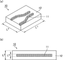
- the wiring board of the present disclosure only needs to have a structure in which the dielectric line is covered with the dielectric exterior portion.
- a structure having the body track 11 is given.
- Such a structure can be created, for example, by forming a cavity from the side surface of the dielectric sheath that is equal to or larger than the outer dimension of the dielectric line, and then inserting an inner layer.
- a dielectric line may be formed by using a laser or an electron beam to increase the dielectric constant of the outer layer at the position of the inner layer to a temperature equal to or higher than the melting point of the material forming the outer layer.
- the dielectric exterior part has a laminated structure of a lower layer having a groove for housing the dielectric line and an upper layer formed on the lower layer. is there.
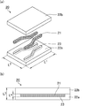
- the wiring board 20 may include the lower layer 22a having the groove 23 for housing the dielectric line 21, the dielectric line 21 being housed therein, and the upper layer 22b being laminated.
- a metal mold having the same shape as that of the dielectric line may be pressed against the lower layer to burn a part of the lower layer to increase the dielectric constant, thereby forming the dielectric line.
- the wiring board has an adhesive layer between the lower layer and the upper layer of the dielectric exterior portion.
- an adhesive layer between the lower layer and the upper layer of the dielectric exterior portion.
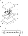
- FIG. 3 a mode in which the wiring board 30 has a groove 33 for accommodating the dielectric line 31 and an adhesive layer 34 between the lower layer 32a and the upper layer 32b can be mentioned.
- the adhesive layer is provided between the lower layer and the upper layer of the dielectric exterior part as described above, the thickness of the dielectric exterior part in this specification is as shown in L 3 of FIG. , The total thickness of the upper layer and the adhesive layer.
- the relative permittivity of the material forming the adhesive layer is not particularly limited as long as it is appropriately determined depending on the relative permittivity of the dielectric line and the dielectric sheath, but the relative permittivity of the material may be lower than that of the dielectric line. preferable.
- the dielectric loss tangent of the material forming the adhesive layer at 6 GHz and 25° C. is preferably 0.003 or less, more preferably 0.002 or less, and even more preferably 0.0015 or less. ..
- the dissipation factor can be measured using a cavity resonator.
- the material forming the adhesive layer is selected from the group consisting of polytetrafluoroethylene, tetrafluoroethylene/hexafluoropropylene copolymer, tetrafluoroethylene/perfluoro(alkyl vinyl ether) copolymer, polyethylene, and polypropylene. At least one of the above is preferable. More preferably, it is at least one selected from the group consisting of tetrafluoroethylene/perfluoro(alkyl vinyl ether) copolymer (PFA), polypropylene, and polyethylene.
- PFA tetrafluoroethylene/perfluoro(alkyl vinyl ether) copolymer
- Y 1 represents F or CF 3
- R f1 represents a perfluoroalkyl group having 1 to 5 carbon atoms
- p represents an integer of 0 to 5
- q represents an integer of 0 to 5.
- CFX CXOCF 2 OR 1 (2)
- X is the same or different and represents H, F or CF 3
- R 1 is at least one atom selected from the group consisting of H, Cl, Br and I, which is linear or branched.
- It may contain 1 to 2 fluoroalkyl groups having 1 to 6 carbon atoms, or 1 or 2 at least one atom selected from the group consisting of H, Cl, Br and I. It represents a cyclic fluoroalkyl group having a good carbon number of 5 or 6.) At least one selected from the group consisting of
- PAVE perfluoro(propyl vinyl ether)
- the PFA preferably contains more than 1.0% by mass of PAVE units based on all polymerized units. Further, it is preferable that the PAVE unit is contained in an amount of 10% by mass or less based on all polymerized units.
- the amount of the PAVE unit is more preferably 2.0% by mass or more, further preferably 3.5% by mass or more, particularly preferably 4.0% by mass or more, and 5.0% by mass or more, based on all polymerized units. Is most preferable, 8.0% by mass or less is more preferable, 7.0% by mass or less is further preferable, 6.5% by mass or less is particularly preferable, and 6.0% by mass or less is most preferable.
- the amount of the PAVE unit is measured by the 19 F-NMR method.
- the PFA preferably has a melting point of 280 to 322°C.
- the melting point is more preferably 290°C or higher, and further preferably 315°C or lower.
- the melting point is the temperature corresponding to the maximum value in the heat of fusion curve when the temperature is raised at a rate of 10° C./min using a differential scanning calorimeter [DSC].
- the PFA preferably has a glass transition temperature (Tg) of 70 to 110°C.
- the glass transition temperature is more preferably 80°C or higher, and more preferably 100°C or lower.
- the glass transition temperature is a value obtained by measurement by dynamic viscoelasticity measurement.
- a wiring board having an adhesive layer between the upper layer and the lower layer can be formed by inserting a sheet made of the above material between the lower layer and the upper layer and heating and pressing the sheet.
- the heating and pressurizing conditions may be appropriately selected depending on the material, but for example, the heating temperature is preferably a temperature above the melting point of the above material.
- the thickness of the adhesive layer is preferably 10 to 100 ⁇ m. If the thickness of the adhesive layer is too thin, the adhesiveness may decrease, and if it is too thick, the transmission loss may increase. More preferably, it is 20 to 60 ⁇ m.
- the dielectric exterior part has a laminated structure of a lower layer, an intermediate layer having a cavity for accommodating a dielectric line formed on the lower layer, and an upper layer formed on the intermediate layer. It is also preferable to have
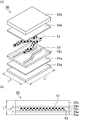
- the wiring board 40 may have a mode in which the dielectric line 41 is housed and the upper layer 42b is stacked in an intermediate layer 42c having a cavity 43 for housing the dielectric line 41.
- the dielectric exterior part preferably has an adhesive layer between the lower layer and the intermediate layer or between the intermediate layer and the upper layer, and between the lower layer and the intermediate layer and between the intermediate layer and the upper layer. It is more preferred to have an adhesive layer both between and between the layers.
- the wiring board 50 accommodates the dielectric line 51 in an intermediate layer 52c having a cavity 53 for accommodating the dielectric line 51, and bonds between the upper layer 52b and the intermediate layer 52c.
- An embodiment in which the layer 54b is provided and the adhesive layer 54a is provided between the intermediate layer 52c and the lower layer 52a is also included.
- the same adhesive layer as described above can be used as the adhesive layer.
- the thickness of the dielectric sheath in this specification is L 3 in FIG. As shown in, the total thickness of the lower layer, the intermediate layer, the upper layer and the adhesive layer.
- the wiring board of the present disclosure includes a dielectric line containing polytetrafluoroethylene and a dielectric exterior part covering the dielectric line containing polytetrafluoroethylene, and the dielectric exterior part has a ratio at 6 GHz and 25°C. It is one of the preferable modes that the permittivity is lower than that of the dielectric line.
- the polytetrafluoroethylene contained in the dielectric line and the polytetrafluoroethylene contained in the dielectric sheath may be the same or different.
- the relative permittivity, hardness, etc. of the dielectric line and the dielectric exterior part can be adjusted by molding conditions, materials other than polytetrafluoroethylene, and the like.
- the relative dielectric constant of the dielectric line may be made higher than that of the dielectric exterior part by incorporating a high dielectric constant inorganic powder into the PTFE forming the dielectric line, or the dielectric line may be a PTFE paste. It is manufactured by extrusion molding and firing, and the dielectric exterior part is formed by solidifying sinter and crushed powder of PTFE to reduce the density of the dielectric exterior part, and the relative dielectric constant of the dielectric exterior part It can be lower than the track. Further, even if the dielectric constant is low, it can be self-supporting and can hold electronic components.
- the PTFE contained in the dielectric line may be semi-sintered PTFE.
- the dielectric line containing semi-baked PTFE is obtained, for example, by a step of paste-extruding a powder of unbaked PTFE to obtain an unbaked PTFE molded body, and the unbaked PTFE molded body at 320 to 340° C. for 10 seconds to 180 seconds. It can be manufactured by a method including a step of obtaining a PTFE molded body containing semi-baked PTFE by firing for minutes.
- the manufacturing method may include a step of molding a PTFE molded body containing semi-baked PTFE into a shape of a dielectric line.
- Specific heating conditions are appropriately changed depending on the shape and size of the PTFE molded body. For example, it is preferably obtained by heating unsintered PTFE at 326 to 345° C. for 10 seconds to 2 hours.
- the heating temperature is more preferably 330° C. or higher.
- the unsintered PTFE is PTFE that has no history of being heated to 326° C. or higher, and is preferably PTFE that has no history of being heated to 300° C. or higher.
- the air contained in the unsintered PTFE is released to the outside, and it is presumed that a PTFE molded product having a high relative dielectric constant can be obtained.
- unsintered PTFE is not completely sintered, it is presumed that a PTFE molded product having a low dielectric loss tangent can be obtained.
- the above heating can be performed using a salt bath, a sand bath, a hot air circulation type electric furnace, or the like.
- the semi-sintered PTFE molded product is preferably obtained by heating unsintered PTFE without heating it to higher than 345°C. Even if it is heated to more than 345°C even once, the crystallinity originally possessed by unsintered PTFE may be collapsed, and a PTFE molded product having a high crystallinity may not be obtained.
- a PTFE molded body obtained by heating unsintered PTFE at 326 to 345° C. for 10 seconds to 2 hours without heating it to more than 345° C. has a crystallinity similar to that of unsintered PTFE. And has a high relative permittivity and a low dielectric loss tangent.
- the above-mentioned unsintered PTFE molded product is preferably obtained by paste extrusion molding a mixture of unsintered PTFE powder and an extrusion aid.
- the extrusion aid may be removed by drying the obtained extrudate after paste extrusion molding.
- the above mixture may be obtained by mixing unsintered PTFE powder and an extrusion aid by a known method, aging for 1 to 24 hours, and preforming at a pressure of 0.5 to 2.0 MPa. Good.
- the paste extrusion can be performed at an extrusion pressure of 2 to 100 MPa.
- the heating time of the unsintered PTFE differs depending on the diameter of the unsintered PTFE, the heating temperature, and the equipment used for heating. For example, when heating in a hot air circulation type electric furnace, 3 minutes to 2 hours is preferable, and 10 minutes to 30 minutes is more preferable.
- a step of paste-extruding a mixture of unsintered PTFE powder and an extrusion aid to obtain an unsintered PTFE compact, and drying the unsintered PTFE compact to remove the extrusion aid It is preferable to include a step of heating, a step of heating the dried molded body at 326 to 345° C. for 10 seconds to 2 hours, and a step of manufacturing a dielectric line using the PTFE molded body.
- the above manufacturing method does not include any step of heating unsintered PTFE to more than 345° C. in order to obtain a molded product having a high relative dielectric constant and a low dielectric loss tangent.
- the method of manufacturing a dielectric line using the above-mentioned PTFE molded body will differ depending on the characteristics required for the dielectric line, and will be described later in Experimental Examples and the like.
- the dielectric exterior part can be obtained by molding PTFE.
- PTFE can be obtained by a method in which PTFE powder is put in a mold and compression-molded by heating and pressing.
- the heating temperature is preferably the melting point of PTFE or higher, more preferably 340° C. or higher, even more preferably 350° C. or higher. Further, it is preferably 380°C or lower.
- the pressure applied is preferably 10 g/cm 2 or more, more preferably 20 g/cm 2 or more, and further preferably 30 g/cm 2 or more. Further, it is preferably 3000 g/cm 2 or less.
- the PTFE contained in the above-mentioned dielectric exterior part is preferably obtained by compression-molding sintered pulverized powder of PTFE.
- the sinter pulverized powder of PTFE can be obtained by a sinter pulverization method. By using the sinter pulverized powder, it is possible to easily form the dielectric exterior part having a low relative permittivity and a low dielectric loss tangent and a hardness capable of holding an electronic component.
- the sintered pulverized powder preferably has an average particle size of 50 to 3000 ⁇ m.
- the average particle diameter is more preferably 100 ⁇ m or more, further preferably 300 ⁇ m or more, more preferably 2000 ⁇ m or less, and further preferably 1500 ⁇ m or less.
- the average particle diameter is measured by using a laser diffraction particle size distribution analyzer (HELOS & RODOS) manufactured by JEOL Ltd. without using a cascade and at a dispersion pressure of 3.0 bar, and corresponds to 50% of particle size distribution integration. Equal to the particle size.
- HELOS & RODOS laser diffraction particle size distribution analyzer
- the sinter pulverized powder can be obtained, for example, by subjecting PTFE powder to a heat treatment at a temperature equal to or higher than the melting point for 0.1 to 10 hours, and then pulverizing the obtained solid material.
- the temperature of the heat treatment is more preferably 340°C or higher, further preferably 350°C or higher. Further, it is more preferably 380°C or lower.
- the above pulverization can be carried out, for example, by a mixer, an air jet mill or the like. Grinding conditions are not particularly limited.
- the upper layer and the lower layer are produced by the above-mentioned method, etc., and then these are overlaid and heated and pressed. can do.
- an adhesive layer it can be produced by superposing the upper layer, the adhesive layer and the lower layer, and heating and pressing.
- the upper layer, the intermediate layer and the lower layer, or the upper layer, the adhesive layer, the intermediate layer, the adhesive layer and the lower layer can be similarly prepared.
- the adhesive layer is preferably a layer made of PFA because of excellent transmission efficiency and low loss.
- the heating and pressurizing may be performed so long as the upper layer and the lower layer, the upper layer and the intermediate layer, and the intermediate layer and the lower layer are bonded to each other.
- the pressure is 10 g/cm 2 or more.
- End processing method The end portion of the dielectric line may be treated, for example, by adding a 1/4 ⁇ metal rod to the end of the dielectric line, as in the case of the dielectric line coupling device described in Japanese Patent Laid-Open No. 11-186818. Good.
- the coaxial cable may be connected by a method such as waveguide coaxial conversion.
- the wiring board of the present disclosure can be used, for example, as a printed wiring board for high frequency transmission, and the printed board may be formed by bonding a metal foil such as a copper foil.
- the wiring board of the present disclosure will be described by way of examples, but the wiring board of the present disclosure is not limited to such examples.
- Relative permittivity and dielectric loss tangent (tan ⁇ ) The dielectric constant and dielectric loss tangent (tan ⁇ ) of the dielectric line and the exterior are measured by a cavity resonator (6 GHz) manufactured by Kanto Electronics Co., Ltd. and calculation software.
- Hardness Hardness was measured with a durometer type D specified in JIS K6253-2012.
- Example 1 [Method for manufacturing dielectric line] A PTFE paste was prepared by mixing 410 g of a hydrocarbon solvent with 1 kg of polytetrafluoroethylene fine powder having a standard specific gravity (SSG) of 2.175. Next, the above PTFE paste was molded by paste extrusion molding using an extrusion die having an extrusion shape of 10 mm ⁇ 10 mm to obtain a PTFE molded body having a cross section of 10 mm ⁇ 10 mm. The obtained PTFE molded body was placed in a hot air electric furnace and the temperature was raised stepwise from 100°C to 250°C to evaporate and remove the hydrocarbon solvent. The dried cylindrical PTFE molded body was placed in a hot air electric furnace heated to 337° C.
- SSG standard specific gravity
- the cross section after firing was 10.5 mm ⁇ 10.5 mm.
- This molded body was cut into 100 mm to form a dielectric line (inner layer).
- the relative permittivity and dielectric loss tangent of the obtained dielectric line at 6 GHz and 25° C. were 2.18 and 0.00010, respectively.
- the specific gravity of the dielectric line was 2.195.
- this sintered pulverized powder is subjected to heat treatment under pressure to have a thickness of 100 mm ⁇ 100 mm, a weight of 108 g, a specific gravity of 1.0, 6 GHz, a relative dielectric constant of 1.50 at 25° C., and a dielectric loss tangent of 0.0001.
- An outer layer B having a hardness of 75 was obtained.
- An assembly D was obtained by hollowing out a hole of 10.5 mm ⁇ 70 mm in the center of the outer layer A in the thickness direction and fitting the dielectric line (inner layer) produced above in that portion. Thereafter, the outer layer B/PFA sheet having a thickness of 7.5 mm (relative permittivity 2.12, dielectric loss tangent 0.0012) 25 ⁇ m/assembly D/PFA sheet (relative permittivity 2.12, dielectric loss tangent 0.0012) 25 ⁇ m/ The 7.5 mm thick outer layer B was pressurized and heated in a hot air electric furnace at 350° C.
- the relative permittivity and the dielectric loss tangent of the dielectric exterior portion obtained by measuring the relative permittivity and the dielectric loss tangent of the portion excluding the dielectric line portion by the 6 GHz cavity resonator method are respectively 1 It was 0.52 and 0.00015.
- Reference example 1 [Higher dielectric constant of dielectric line] Polytetrafluoroethylene fine powder having a standard specific gravity (SSG) of 2.175 was mixed with alumina having a specific gravity of 3.97 in an amount of 10 vol %, and a hydrocarbon solvent was mixed to prepare a PTFE paste. Next, a mold having a cylinder diameter of 25 mm was filled with the PTFE paste, and the PTFE paste was molded by paste extrusion molding using an extrusion die having an extrusion shape having a diameter of 1.8 mm to obtain a PTFE molded product having a diameter of 1.8 mm.
- SSG standard specific gravity
- the obtained PTFE molded body was placed in a hot air electric furnace and the temperature was raised stepwise from 100°C to 250°C to evaporate and remove the hydrocarbon solvent. After that, it was placed in a hot air electric furnace set at 360° C., fired for 5 minutes, cooled to 270° C. at a rate of 5° C. per hour, and further cooled to room temperature at a rate of 20° C. per hour.
- the electrical characteristics of the obtained PTFE molded product were measured by a dielectric resonator and a dielectric loss tangent (tan ⁇ ) using a cavity resonator manufactured by Kanto Electronics Co., Ltd.
- the relative dielectric constant and dielectric loss tangent of the above-molded PTFE molded body at 6 GHz and 25° C. were 2.36 and 0.0002, respectively.
- Reference example 2 A PTFE molded body was obtained by performing the same operations as in Reference Example 1 except that alumina was not added.
- the relative dielectric constant and dielectric loss tangent of the PTFE molded product molded above at 6 GHz and 25° C. were 2.01 and 0.0002, respectively.
- Dielectric line 12 Dielectric exterior parts 22a, 32a, 42a, 52a: Lower layers 22b, 32b of the dielectric exterior part, 42b, 52 b: dielectric exterior portion of the upper layer 42c, 52c: interlayer 34,54a, 54b: adhesive layers 23,33,43,53: groove
- L 1 length of the dielectric exterior side
- L 2 dielectric sheath short side parts
- L 3 the thickness of the dielectric exterior portion
- L a thickness of dielectric waveguide
Landscapes
- Chemical & Material Sciences (AREA)
- Health & Medical Sciences (AREA)
- Chemical Kinetics & Catalysis (AREA)
- Medicinal Chemistry (AREA)
- Polymers & Plastics (AREA)
- Organic Chemistry (AREA)
- Engineering & Computer Science (AREA)
- Manufacturing & Machinery (AREA)
- Compositions Of Macromolecular Compounds (AREA)
- Laminated Bodies (AREA)
- Waveguides (AREA)
Abstract
Description
上記誘電体外装部は、下部層と上部層との間に接着層を有することが好ましい。上記接着層を構成する材料は、6GHz、25℃における誘電正接が0.003以下であることが好ましく、ポリテトラフルオロエチレン、テトラフルオロエチレン/ヘキサフルオロプロピレン共重合体、テトラフルオロエチレン/パーフルオロ(アルキルビニルエーテル)共重合体、ポリエチレン、及び、ポリプロピレンからなる群より選択される少なくとも1種であることがより好ましい。
上記誘電体線路は、誘電体線路よりも低い比誘電率を有する誘電体外装部に覆われていることによって、ミリ波、サブミリ波等の高周波を効率よく伝送することができる。誘電体外装部は、誘電体線路の表面積の95%以上を覆っていることが好ましく、99%以上を覆っていることがより好ましく、実質的に全面を覆っていることが好ましい。
誘電体線路および誘電体外装部の比誘電率は、直径2mmの円柱状に加工し、空洞共振器を使用して測定することができる。
図6に示すように、断面積がd1(mm)×d2(mm)である線路61が曲線である場合、曲率半径a(mm)で配線板内での曲がりを表すことができる。比誘電率の比と配線板内での曲がりによる伝送損失の関係を表1に示す。

誘電体線路におけるPTFEは、比重が2.160以上であることが好ましく、2.165以上であることがより好ましく、2.170以上であることが更に好ましい。上限は、特に限定されないが、2.30であってよい。
CF2=CF-ORf
(式中、Rfは、パーフルオロ有機基を表す。)で表されるパーフルオロ不飽和化合物等が挙げられる。本明細書において、上記「パーフルオロ有機基」とは、炭素原子に結合する水素原子が全てフッ素原子に置換されてなる有機基を意味する。上記パーフルオロ有機基は、エーテル酸素を有していてもよい。
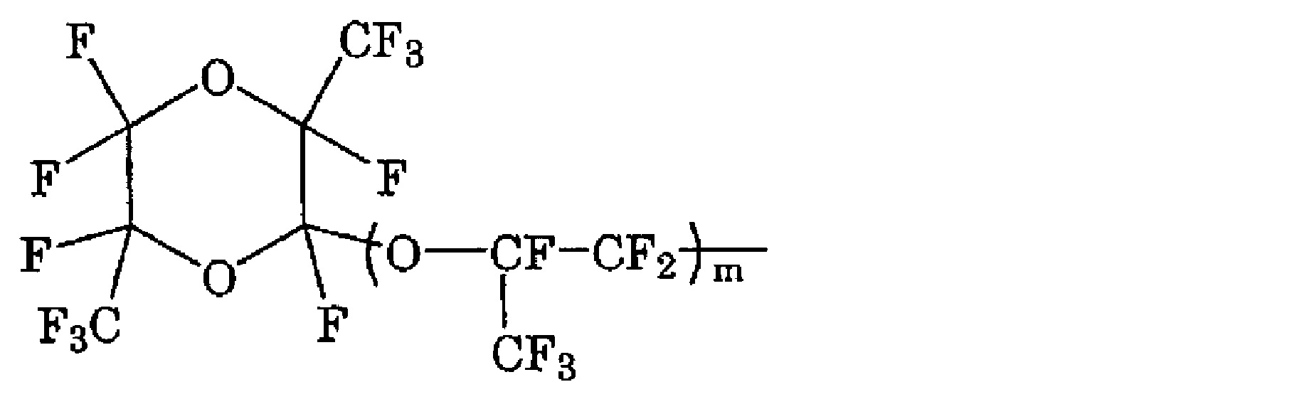

上記比重は、液中ひょう量法(JIS Z 8807準拠)により測定する。
上記結晶化度は、比重法により測定する。
例えば、方形の場合、28GHzの高周波を伝送するためには、各辺の長さが6.9~7.5mmであることが好ましく、この好適な値は周波数と反比例し、例えば、84GHzである場合には2.3~2.5mmであることが好ましい。
誘電体外装部の材料である樹脂(B)の比誘電率及び誘電正接は、樹脂(B)を直径2mmの円柱状に加工し、空洞共振器を使用して測定することができる。
上記誘電体外装部を構成する材料としてより具体的には、PTFEの焼結粉砕粉を圧縮成形したものや、延伸PTFE多孔質体、発泡ポリエチレン等が挙げられる。
上記PTFEの焼結粉砕粉を圧縮成形したものについては、後述する。
上記延伸PTFE多孔質体は、シート状のPTFE成形体を延伸することによって得られる延伸PTFE多孔質膜であってもよい。上記延伸PTFE多孔質体は、従来公知の方法で作製することができる。上記延伸PTFE多孔質体の比誘電率及び誘電正接は、延伸倍率、延伸速度、延伸温度等の延伸条件によって適宜コントロールすることができる。例えば、延伸倍率が高いほど、比誘電率及び誘電正接はともに低下する。
上記比重は、液中ひょう量法(JIS Z 8807準拠)により測定する。
上記結晶化度は、比重法により測定する。
上記誘電体外装部が板状である場合、誘電体外装部の厚みは、誘電体線路の断面が方形である場合はその長辺、円形である場合は長径の0.5~1.5倍であることが好ましい。
上記誘電体外装部が板状である場合、長辺の長さが厚みの3倍以上であることが好ましい。長辺の長さは、厚みの4倍以上であることが好ましく、5倍以上であることがより好ましい。
上記硬度は、JIS K6253-2012に規定されていたデュロメータ タイプDにより測定する。
以下、本開示の配線板の構成についてより詳細に説明する。
このような構造は、例えば、誘電体外装の側面から、誘電体線路の外形寸法と同じ又はそれより大きい空洞を作成した後、内層を入れることにより作成することができる。
また、レーザーや電子線を用い、内層となる位置の外装部を、外装部構成材料の融点以上の温度とすることで高誘電率化して誘電体線路を形成してもよい。
例えば、図2に示すように、配線板20が、誘電体線路21を収納する溝23を有する下部層22aに、誘電体線路21を収納し、上部層22bを積層した態様が挙げられる。
また、下部層に誘電体線路と同じ形状の金属金型を押し付けることで下部層の一部を焼成し、高誘電率化して誘電体線路を形成してもよい。
なお、上記のように誘電体外装部の下部層及び上部層との間に接着層を有する場合、本明細書における誘電体外装部の厚みは、図3のL3に示すように、下部層、上部層及び接着層との合計の厚みである。
上記誘電正接は、空洞共振器を使用して測定することができる。
CF2=CFO(CF2CFY1O)p-(CF2CF2CF2O)q-Rf1 (1)
(式中、Y1はF又はCF3を表し、Rf1は炭素数1~5のパーフルオロアルキル基を表す。pは0~5の整数を表し、qは0~5の整数を表す。)、及び、一般式(2):
CFX=CXOCF2OR1 (2)
(式中、Xは、同一又は異なり、H、F又はCF3を表し、R1は、直鎖又は分岐した、H、Cl、Br及びIからなる群より選択される少なくとも1種の原子を1~2個含んでいてもよい炭素数が1~6のフルオロアルキル基、若しくは、H、Cl、Br及びIからなる群より選択される少なくとも1種の原子を1~2個含んでいてもよい炭素数が5又は6の環状フルオロアルキル基を表す。)
からなる群より選択される少なくとも1種を挙げることができる。
上記PAVE単位の量は、全重合単位に対して、2.0質量%以上がより好ましく、3.5質量%以上が更に好ましく、4.0質量%以上が特に好ましく、5.0質量%以上が最も好ましく、8.0質量%以下がより好ましく、7.0質量%以下が更に好ましく、6.5質量%以下が特に好ましく、6.0質量%以下が最も好ましい。
なお、上記PAVE単位の量は、19F-NMR法により測定する。
上記融点は、290℃以上であることがより好ましく、315℃以下であることがより好ましい。
上記融点は、示差走査熱量計〔DSC〕を用いて10℃/分の速度で昇温したときの融解熱曲線における極大値に対応する温度である。
上記ガラス転移温度は、動的粘弾性測定により測定して得られる値である。
上記接着層としては上述したものと同じものを採用できる。
上記のように誘電体外装部の下部層と中間層との間、中間層と上部層との間に接着層を有する場合、本明細書における誘電体外装部の厚みは、図5のL3に示すように、下部層、中間層、上部層及び接着層との合計の厚みである。
上記誘電体線路に含まれるポリテトラフルオロエチレンと誘電体外装部に含まれるポリテトラフルオロエチレンは同じでもよいし異なってもよい。
誘電体線路と誘電体外装部の比誘電率、硬度等は、成形条件やポリテトラフルオロエチレン以外の材料等によって調整することができる。
具体的な加熱条件は、PTFE成形体の形状及び大きさにより適宜変更する。例えば、未焼成PTFEを326~345℃で10秒~2時間加熱することにより得られるものであることが好ましい。加熱温度は、330℃以上であることがより好ましい。
上記温度で所定時間加熱することにより、未焼成PTFEが含んでいた空気が外部に放出されるため、高い比誘電率を有するPTFE成形体を得ることができると推測される。また、未焼成PTFEを完全に焼成しないので、低い誘電正接を有するPTFE成形体を得ることができると推測される。
上記の加熱は、ソルトバス、サンドバス、熱風循環式電気炉等を使用して行うことができる。
上記未焼成PTFEの加熱時間は、上記未焼成PTFEの直径、加熱温度、加熱に使用する設備によって異なる。
例えば、熱風循環式電気炉で加熱する場合は3分~2時間が好ましく、10分~30分がより好ましい。
上記PTFE成形体を用いて誘電体線路を製造する方法については、誘電体線路に要求される特性によって相違するので、後述する実験例等で説明する。
上記加熱温度はPTFEの融点以上であることが好ましく、340℃以上であることがより好ましく、350℃以上であることが更に好ましい。また、380℃以下が好ましい。
上記加圧の圧力は、例えば、10g/cm2以上であることが好ましく、20g/cm2以上であることがより好ましく、30g/cm2以上であることが更に好ましい。また、3000g/cm2以下が好ましい。
PTFEの焼結粉砕粉は、焼結粉砕法により得ることができる。焼結粉砕粉を用いることによって、低比誘電率及び低誘電正接であり、かつ、電子部品を保持可能な硬さを備える誘電体外装部を容易に形成することができる。
上記平均粒子径は、日本電子株式会社製レーザー回折式粒度分布測定装置(HELOS&RODOS)を用いて、カスケードは使用せず、分散圧力3.0barで測定を行い、粒度分布積算の50%に対応する粒子径に等しいとする。
上記熱処理の温度は340℃以上がより好ましく、350℃以上が更に好ましい。また、380℃以下がより好ましい。
上記粉砕は、例えば、ミキサー、エアジェットミル等により実施できる。粉砕の条件は特に限定されない。
上記加熱及び加圧は上部層と下部層、上部層と中間層、中間層と下部層とが接着するものであればよく、例えば、接着層を構成する材料の融点以上の温度であることが好ましく、圧力は10g/cm2以上であることが好ましい。
誘電体線路の端部は、例えば、特開平11-186818号公報に記載された誘電体線路結合装置と同様に、1/4λの金属棒を誘電体線路端に添わせることにより処理してもよい。また、導波管同軸変換を行う方法等によって同軸ケーブルと接続してもよい。
誘電体線路及び外装の比誘電率測定及び誘電正接(tanδ)の測定は、株式会社関東電子応用開発製空洞共振器(6GHz)と計算ソフトによる。
JIS K6253-2012に規定されていたデュロメータ タイプDにより硬さを測定した。
液中ひょう量法(JIS Z 8807準拠)により測定した。
[誘電体線路の作製方法]
標準比重(SSG)が2.175であるポリテトラフルオロエチレンファインパウダー1kgに、炭化水素系溶剤を410g混合して、PTFEペーストを作製した。次に、10mm×10mmの押出形状をもつ押出ダイを用いて、ペースト押出成形により上記PTFEペーストを成形して、断面が10mm×10mmのPTFE成形体を得た。得られたPTFE成形体を熱風電気炉内に設置して、100℃から250℃へ段階的に温度上昇させ、炭化水素系溶剤を蒸散除去させた。
乾燥後の円柱状PTFE成形体を337℃に熱した熱風電気炉へ入れて2時間焼成を行い、円柱状PTFE成形体を得た。焼成後の断面は10.5mm×10.5mmであった。この成形体を100mmに切断して誘電体線路(内層)とした。
得られた誘電体線路の6GHz、25℃における比誘電率及び誘電正接はそれぞれ2.18、0.00010であった。誘電体線路の比重は、2.195であった。
標準比重(SSG)が2.175であるポリテトラフルオロエチレンファインパウダー1kgをステンレス容器に入れて、熱風電気炉によって360℃3時間熱処理する。できた固形物をさらに食品ミキサーに入れ粉砕し、8メッシュのステンレスメッシュに通すことで粒径が1.7mm以下であるPTFE焼結粉砕粉を作製した。
この焼結粉砕粉108gを、110mm×110mmのステンレス金型で均一に入れて4416gの上金型で加圧(36.5g/cm2)しながら360℃の熱風電気炉に3時間入れ、常温まで放熱後に成形物を取り出した。
その結果、10mm厚みの100mm×100mm、重量108g、比重1.0、6GHz、25℃における比誘電率1.50、誘電正接0.0001、硬度95である誘電体外装部の外層Aを得た。
同様にこの焼結粉砕粉78gを加圧熱処理することで7.5mm厚みの100mm×100mm、重量108g、比重1.0、6GHz、25℃における比誘電率1.50、誘電正接0.0001、硬度75である外層Bを得た。
外層Aの中心部に10.5mm×70mmの穴を厚み方向にくりぬいてその部分に上記で作製した誘電体線路(内層)をはめ込んで、組立品Dを得た。その後、7.5mm厚の外層B/PFAシート(比誘電率2.12、誘電正接0.0012)25μm/組立品D/PFAシート(比誘電率2.12、誘電正接0.0012)25μm/7.5mm厚外層Bを上記の上金型(4416g)で加圧(36.5g/cm2)しながら、350℃3時間熱風電気炉にて加圧加熱した。得られた配線板において、誘電体線路部を除いた部分の比誘電率及び誘電正接を6GHz空洞共振器法で測定することにより求めた誘電体外装部の比誘電率及び誘電正接は、それぞれ1.52、0.00015であった。
上記で成形した10mm×10mm長さ100mmの誘電体線路の両端10mmを四角錐状に切断し、方形導波管同軸変換器内へ挿入し、伝送損失を測定したところ、28GHzにおいて伝送損失が-2dBであった。
(参考:通常高周波で使われるLCP基板100mmに、28GHzの電磁波を通すと、-5~-7dBの伝送損失となる。)
[誘電体線路の高誘電率化]
標準比重(SSG)が2.175であるポリテトラフルオロエチレンファインパウダーに、比重3.97のアルミナを10vol%となるように混合し、炭化水素系溶剤を混合して、PTFEペーストを作製した。次に、シリンダー径25mmの金型にPTFEペーストを充填し、直径1.8mmの押出形状を持つ押出ダイを用いて、ペースト押出成形によりPTFEペーストを成形して、直径1.8mmのPTFE成形体を得た。得られたPTFE成形体を熱風電気炉内に設置して、100℃から250℃へ段階的に温度上昇させ、炭化水素系溶剤を蒸散除去させた。その後、360℃に設定した熱風電気炉内に設置して5分間焼成後、1時間あたり5℃の速度で270℃まで降温し、さらに1時間あたり20℃の速度で室温まで降温した。
アルミナは1MHzにおける比誘電率、誘電正接がそれぞれ10、0.0002のものを用いた。
得られたPTFE成形体の電気特性を比誘電率測定及び誘電正接(tanδ)の測定は、株式会社関東電子応用開発製空洞共振器により測定した。
上記で成形したPTFE成形体の6GHz、25℃における比誘電率及び誘電正接はそれぞれ2.36、0.0002だった。
参考例1にアルミナを添加しないこと以外はすべて同じ操作を行いPTFE成形体を得た。
上記で成形したPTFE成形体の6GHz、25℃における比誘電率及び誘電正接はそれぞれ2.01、0.0002だった。
11、21、31、41、51:誘電体線路
12:誘電体外装部
22a、32a、42a、52a:誘電体外装部の下部層
22b、32b、42b、52b:誘電体外装部の上部層
42c、52c:中間層
34、54a、54b:接着層
23、33、43、53:溝
L1:誘電体外装部の長辺
L2:誘電体外装部の短辺
L3:誘電体外装部の厚み
La:誘電体線路の厚み
Claims (21)
- 樹脂(A)を含む誘電体線路と、該誘電体線路を覆い、樹脂(B)を含む誘電体外装部とを備え、
前記誘電体外装部は、6GHz、25℃における比誘電率が前記誘電体線路よりも低いことを特徴とする配線板。 - 6GHz、25℃における誘電体外装部の比誘電率と誘電体線路の比誘電率との比(誘電体外装部の比誘電率/誘電体線路の比誘電率)が、0.60~0.90である請求項1記載の配線板。
- 前記樹脂(A)は、6GHz、25℃における比誘電率が3.0以下であり、誘電正接が0.003以下である請求項1又は2記載の配線板。
- 前記樹脂(A)は、ポリテトラフルオロエチレン、テトラフルオロエチレン/ヘキサフルオロプロピレン共重合体、テトラフルオロエチレン/パーフルオロ(アルキルビニルエーテル)共重合体、ポリプロピレン及びポリエチレンからなる群より選択される少なくとも1種である請求項1~3のいずれかに記載の配線板。
- 前記誘電体線路は、更に、無機粉体(C)を含み、6GHz、25℃における比誘電率が2.2以上である請求項1~4のいずれかに記載の配線板。
- 無機粉体(C)は、セラミック粉体である請求項5記載の配線板。
- 無機粉体(C)は、チタン酸バリウム系、チタン酸ストロンチウム系、チタン酸カルシウム系、チタン酸マグネシウム系、チタン酸ジルコニウム系、チタン酸ランタン系、チタン酸ビスマス系、Ba(Mg1/3Ta2/3)O3系、Ba(Zn1/3Ta2/3)O3系、CaTiO3-(Li1/2Nd1/2)TiO3-(Li1/2Bi1/2)TiO3系、タンタル酸マグネシウム系、ニオブ酸マグネシウム系、アルミナ系、マグネシア系、チタニア系、酸化タンタル系、酸化ニオブ系、フェライト系、ジルコニア系、及び、希土類複合酸化物系からなる群より選択される少なくとも1種である請求項5又は6記載の配線板。
- 前記樹脂(B)は、6GHz、25℃における誘電体線路の比誘電率よりも小さく、誘電正接が0.0012以下である請求項1~7のいずれかに記載の配線板。
- 前記樹脂(B)は、ポリテトラフルオロエチレン、テトラフルオロエチレン/ヘキサフルオロプロピレン共重合体、テトラフルオロエチレン/パーフルオロ(アルキルビニルエーテル)共重合体、ポリプロピレン、ポリエチレン、ポリスチレン及びポリスチロールからなる群より選択される少なくとも1種である請求項1~8のいずれかに記載の配線板。
- 前記誘電体外装部は、更に、無機粉体(D)を含み、6GHz、25℃における比誘電率が2.2以上である請求項1~9のいずれかに記載の配線板。
- 無機粉体(D)は、セラミック粉体である請求項10記載の配線板。
- 無機粉体(D)は、チタン酸バリウム系、チタン酸ストロンチウム系、チタン酸カルシウム系、チタン酸マグネシウム系、チタン酸ジルコニウム系、チタン酸ランタン系、チタン酸ビスマス系、Ba(Mg1/3Ta2/3)O3系、Ba(Zn1/3Ta2/3)O3系、CaTiO3-(Li1/2Nd1/2)TiO3-(Li1/2Bi1/2)TiO3系、タンタル酸マグネシウム系、ニオブ酸マグネシウム系、アルミナ系、マグネシア系、チタニア系、酸化タンタル系、酸化ニオブ系、フェライト系、ジルコニア系、及び、希土類複合酸化物系からなる群より選択される少なくとも1種である請求項10又は11記載の配線板。
- 前記誘電体外装部は、誘電体線路を収納する溝を有する下部層と、前記下部層上に形成された上部層との積層構造を有する請求項1~12のいずれかに記載の配線板。
- 前記誘電体外装部は、下部層と上部層との間に接着層を有する請求項13記載の配線板。
- 前記接着層を構成する材料は、6GHz、25℃における誘電正接が0.003以下である請求項14記載の配線板。
- 前記接着層を構成する材料は、ポリテトラフルオロエチレン、テトラフルオロエチレン/ヘキサフルオロプロピレン共重合体、テトラフルオロエチレン/パーフルオロ(アルキルビニルエーテル)共重合体、ポリエチレン、及び、ポリプロピレンからなる群より選択される少なくとも1種である請求項14又は15記載の配線板。
- 前記誘電体外装部は、下部層と、該下部層上に形成された誘電体線路を収納する空洞を有する中間層と、該中間層上に形成された上部層との積層構造を有する請求項1~12のいずれかに記載の配線板。
- 前記誘電体外装部は、下部層と中間層との間、又は、中間層と上部層との間に接着層を有する請求項17記載の配線板。
- 前記接着層を構成する材料は、6GHz、25℃における誘電正接が0.003以下である請求項18記載の配線板。
- 前記接着層を構成する材料は、ポリテトラフルオロエチレン、テトラフルオロエチレン/ヘキサフルオロプロピレン共重合体、テトラフルオロエチレン/パーフルオロ(アルキルビニルエーテル)共重合体、ポリエチレン、及び、ポリプロピレンからなる群より選択される少なくとも1種である請求項18又は19記載の配線板。
- 誘電体外装部は、板状であり、長辺の長さが厚みの3倍以上である請求項1~20のいずれかに記載の配線板。
Priority Applications (4)
| Application Number | Priority Date | Filing Date | Title |
|---|---|---|---|
| KR1020217027463A KR102616049B1 (ko) | 2019-02-01 | 2020-01-30 | 배선판 |
| CN202080010625.XA CN113330635B (zh) | 2019-02-01 | 2020-01-30 | 配线板 |
| JP2020568596A JP7144698B2 (ja) | 2019-02-01 | 2020-01-30 | 配線板 |
| US17/381,681 US12087988B2 (en) | 2019-02-01 | 2021-07-21 | Wiring board |
Applications Claiming Priority (2)
| Application Number | Priority Date | Filing Date | Title |
|---|---|---|---|
| JP2019-017362 | 2019-02-01 | ||
| JP2019017362 | 2019-02-01 |
Related Child Applications (1)
| Application Number | Title | Priority Date | Filing Date |
|---|---|---|---|
| US17/381,681 Continuation US12087988B2 (en) | 2019-02-01 | 2021-07-21 | Wiring board |
Publications (1)
| Publication Number | Publication Date |
|---|---|
| WO2020158868A1 true WO2020158868A1 (ja) | 2020-08-06 |
Family
ID=71841848
Family Applications (1)
| Application Number | Title | Priority Date | Filing Date |
|---|---|---|---|
| PCT/JP2020/003447 Ceased WO2020158868A1 (ja) | 2019-02-01 | 2020-01-30 | 配線板 |
Country Status (5)
| Country | Link |
|---|---|
| US (1) | US12087988B2 (ja) |
| JP (1) | JP7144698B2 (ja) |
| KR (1) | KR102616049B1 (ja) |
| CN (1) | CN113330635B (ja) |
| WO (1) | WO2020158868A1 (ja) |
Citations (3)
| Publication number | Priority date | Publication date | Assignee | Title |
|---|---|---|---|---|
| JPH10163964A (ja) * | 1996-11-29 | 1998-06-19 | Nec Corp | 多数チャンネル並列光伝送システムおよびそれに使用されるマルチモード光導波路の製造方法 |
| US20160240907A1 (en) * | 2015-02-12 | 2016-08-18 | Texas Instruments Incorporated | Dielectric Waveguide Radar Signal Distribution |
| WO2016159314A1 (ja) * | 2015-03-31 | 2016-10-06 | ダイキン工業株式会社 | 誘電体導波線路 |
Family Cites Families (2)
| Publication number | Priority date | Publication date | Assignee | Title |
|---|---|---|---|---|
| JPS6166730A (ja) | 1984-09-07 | 1986-04-05 | Chuko Kasei Kogyo Kk | ポリテトラフルオロエチレン樹脂多孔質体の製造方法 |
| JPH11186818A (ja) | 1997-12-17 | 1999-07-09 | Tdk Corp | 誘電体線路結合装置 |
-
2020
- 2020-01-30 JP JP2020568596A patent/JP7144698B2/ja active Active
- 2020-01-30 KR KR1020217027463A patent/KR102616049B1/ko active Active
- 2020-01-30 WO PCT/JP2020/003447 patent/WO2020158868A1/ja not_active Ceased
- 2020-01-30 CN CN202080010625.XA patent/CN113330635B/zh active Active
-
2021
- 2021-07-21 US US17/381,681 patent/US12087988B2/en active Active
Patent Citations (3)
| Publication number | Priority date | Publication date | Assignee | Title |
|---|---|---|---|---|
| JPH10163964A (ja) * | 1996-11-29 | 1998-06-19 | Nec Corp | 多数チャンネル並列光伝送システムおよびそれに使用されるマルチモード光導波路の製造方法 |
| US20160240907A1 (en) * | 2015-02-12 | 2016-08-18 | Texas Instruments Incorporated | Dielectric Waveguide Radar Signal Distribution |
| WO2016159314A1 (ja) * | 2015-03-31 | 2016-10-06 | ダイキン工業株式会社 | 誘電体導波線路 |
Non-Patent Citations (1)
| Title |
|---|
| ANONYMOUS: "Characteristics of PTFE <electrical characteristics>", SEALQUICKSEARCHER (ENGLISH), 1 January 2019 (2019-01-01), XP055726112, Retrieved from the Internet <URL:https://web.archive.org/web/20190101000000*/http://www.seal.valqua.co.jp/en/fp-property/fluoroplastics_characteristic> [retrieved on 20200323] * |
Also Published As
| Publication number | Publication date |
|---|---|
| KR102616049B1 (ko) | 2023-12-21 |
| CN113330635B (zh) | 2023-05-23 |
| US12087988B2 (en) | 2024-09-10 |
| JP7144698B2 (ja) | 2022-09-30 |
| JPWO2020158868A1 (ja) | 2021-11-18 |
| US20210359386A1 (en) | 2021-11-18 |
| CN113330635A (zh) | 2021-08-31 |
| KR20210118172A (ko) | 2021-09-29 |
Similar Documents
| Publication | Publication Date | Title |
|---|---|---|
| CN107408751B (zh) | 电介质波导线路 | |
| US8883313B2 (en) | Modified polytetrafluoroethylene powder and method for producing tetrafluoroethylene polymer | |
| JP7421156B1 (ja) | 誘電体及びその製造方法 | |
| JP7144698B2 (ja) | 配線板 | |
| JP7626955B2 (ja) | 組成物、シート及びその製造方法 | |
| JP7583342B2 (ja) | 誘電体、銅張積層体及びそれらの製造方法 | |
| US20250230298A1 (en) | Composition, fluororesin sheet, and method for producing same | |
| JP7534688B2 (ja) | 組成物、フッ素樹脂シート及びその製造方法 | |
| JPH07182921A (ja) | 複合誘電体およびプリント回路用基板 | |
| JP7846386B2 (ja) | 誘電体、銅張積層体及びそれらの製造方法 | |
| JPH07272534A (ja) | 複合誘電体の製造方法 | |
| JP2024166544A (ja) | 金属積層板及びその製造方法 | |
| WO2025053138A1 (ja) | シート、その製造方法、金属張積層板、回路用基板及びアンテナ | |
| JP2026069514A (ja) | 誘電体、銅張積層体及びそれらの製造方法 | |
| WO2025187578A1 (ja) | 組成物、ペースト状組成物、シート、金属張積層体、回路基板及びシートの製造方法 | |
| JPS6019604B2 (ja) | 複合誘電体 |
Legal Events
| Date | Code | Title | Description |
|---|---|---|---|
| 121 | Ep: the epo has been informed by wipo that ep was designated in this application |
Ref document number: 20749232 Country of ref document: EP Kind code of ref document: A1 |
|
| ENP | Entry into the national phase |
Ref document number: 2020568596 Country of ref document: JP Kind code of ref document: A |
|
| NENP | Non-entry into the national phase |
Ref country code: DE |
|
| ENP | Entry into the national phase |
Ref document number: 20217027463 Country of ref document: KR Kind code of ref document: A |
|
| 122 | Ep: pct application non-entry in european phase |
Ref document number: 20749232 Country of ref document: EP Kind code of ref document: A1 |