WO2020153275A1 - 測距装置、車載システム及び測距方法 - Google Patents
測距装置、車載システム及び測距方法 Download PDFInfo
- Publication number
- WO2020153275A1 WO2020153275A1 PCT/JP2020/001607 JP2020001607W WO2020153275A1 WO 2020153275 A1 WO2020153275 A1 WO 2020153275A1 JP 2020001607 W JP2020001607 W JP 2020001607W WO 2020153275 A1 WO2020153275 A1 WO 2020153275A1
- Authority
- WO
- WIPO (PCT)
- Prior art keywords
- circuit
- histogram
- unit
- calculation
- vehicle
- Prior art date
- Legal status (The legal status is an assumption and is not a legal conclusion. Google has not performed a legal analysis and makes no representation as to the accuracy of the status listed.)
- Ceased
Links
Images











Classifications
-
- G—PHYSICS
- G01—MEASURING; TESTING
- G01S—RADIO DIRECTION-FINDING; RADIO NAVIGATION; DETERMINING DISTANCE OR VELOCITY BY USE OF RADIO WAVES; LOCATING OR PRESENCE-DETECTING BY USE OF THE REFLECTION OR RERADIATION OF RADIO WAVES; ANALOGOUS ARRANGEMENTS USING OTHER WAVES
- G01S17/00—Systems using the reflection or reradiation of electromagnetic waves other than radio waves, e.g. lidar systems
- G01S17/88—Lidar systems specially adapted for specific applications
- G01S17/93—Lidar systems specially adapted for specific applications for anti-collision purposes
- G01S17/931—Lidar systems specially adapted for specific applications for anti-collision purposes of land vehicles
-
- G—PHYSICS
- G01—MEASURING; TESTING
- G01S—RADIO DIRECTION-FINDING; RADIO NAVIGATION; DETERMINING DISTANCE OR VELOCITY BY USE OF RADIO WAVES; LOCATING OR PRESENCE-DETECTING BY USE OF THE REFLECTION OR RERADIATION OF RADIO WAVES; ANALOGOUS ARRANGEMENTS USING OTHER WAVES
- G01S17/00—Systems using the reflection or reradiation of electromagnetic waves other than radio waves, e.g. lidar systems
- G01S17/02—Systems using the reflection of electromagnetic waves other than radio waves
- G01S17/06—Systems determining position data of a target
- G01S17/08—Systems determining position data of a target for measuring distance only
- G01S17/10—Systems determining position data of a target for measuring distance only using transmission of interrupted, pulse-modulated waves
-
- G—PHYSICS
- G01—MEASURING; TESTING
- G01S—RADIO DIRECTION-FINDING; RADIO NAVIGATION; DETERMINING DISTANCE OR VELOCITY BY USE OF RADIO WAVES; LOCATING OR PRESENCE-DETECTING BY USE OF THE REFLECTION OR RERADIATION OF RADIO WAVES; ANALOGOUS ARRANGEMENTS USING OTHER WAVES
- G01S17/00—Systems using the reflection or reradiation of electromagnetic waves other than radio waves, e.g. lidar systems
- G01S17/88—Lidar systems specially adapted for specific applications
- G01S17/89—Lidar systems specially adapted for specific applications for mapping or imaging
-
- G—PHYSICS
- G01—MEASURING; TESTING
- G01S—RADIO DIRECTION-FINDING; RADIO NAVIGATION; DETERMINING DISTANCE OR VELOCITY BY USE OF RADIO WAVES; LOCATING OR PRESENCE-DETECTING BY USE OF THE REFLECTION OR RERADIATION OF RADIO WAVES; ANALOGOUS ARRANGEMENTS USING OTHER WAVES
- G01S7/00—Details of systems according to groups G01S13/00, G01S15/00, G01S17/00
- G01S7/48—Details of systems according to groups G01S13/00, G01S15/00, G01S17/00 of systems according to group G01S17/00
- G01S7/481—Constructional features, e.g. arrangements of optical elements
- G01S7/4816—Constructional features, e.g. arrangements of optical elements of receivers alone
-
- G—PHYSICS
- G01—MEASURING; TESTING
- G01S—RADIO DIRECTION-FINDING; RADIO NAVIGATION; DETERMINING DISTANCE OR VELOCITY BY USE OF RADIO WAVES; LOCATING OR PRESENCE-DETECTING BY USE OF THE REFLECTION OR RERADIATION OF RADIO WAVES; ANALOGOUS ARRANGEMENTS USING OTHER WAVES
- G01S7/00—Details of systems according to groups G01S13/00, G01S15/00, G01S17/00
- G01S7/48—Details of systems according to groups G01S13/00, G01S15/00, G01S17/00 of systems according to group G01S17/00
- G01S7/483—Details of pulse systems
- G01S7/486—Receivers
- G01S7/4861—Circuits for detection, sampling, integration or read-out
- G01S7/4863—Detector arrays, e.g. charge-transfer gates
-
- G—PHYSICS
- G01—MEASURING; TESTING
- G01S—RADIO DIRECTION-FINDING; RADIO NAVIGATION; DETERMINING DISTANCE OR VELOCITY BY USE OF RADIO WAVES; LOCATING OR PRESENCE-DETECTING BY USE OF THE REFLECTION OR RERADIATION OF RADIO WAVES; ANALOGOUS ARRANGEMENTS USING OTHER WAVES
- G01S7/00—Details of systems according to groups G01S13/00, G01S15/00, G01S17/00
- G01S7/48—Details of systems according to groups G01S13/00, G01S15/00, G01S17/00 of systems according to group G01S17/00
- G01S7/483—Details of pulse systems
- G01S7/486—Receivers
- G01S7/487—Extracting wanted echo signals, e.g. pulse detection
- G01S7/4873—Extracting wanted echo signals, e.g. pulse detection by deriving and controlling a threshold value
-
- G—PHYSICS
- G01—MEASURING; TESTING
- G01S—RADIO DIRECTION-FINDING; RADIO NAVIGATION; DETERMINING DISTANCE OR VELOCITY BY USE OF RADIO WAVES; LOCATING OR PRESENCE-DETECTING BY USE OF THE REFLECTION OR RERADIATION OF RADIO WAVES; ANALOGOUS ARRANGEMENTS USING OTHER WAVES
- G01S7/00—Details of systems according to groups G01S13/00, G01S15/00, G01S17/00
- G01S7/48—Details of systems according to groups G01S13/00, G01S15/00, G01S17/00 of systems according to group G01S17/00
- G01S7/481—Constructional features, e.g. arrangements of optical elements
- G01S7/4817—Constructional features, e.g. arrangements of optical elements relating to scanning
-
- H—ELECTRICITY
- H10—SEMICONDUCTOR DEVICES; ELECTRIC SOLID-STATE DEVICES NOT OTHERWISE PROVIDED FOR
- H10F—INORGANIC SEMICONDUCTOR DEVICES SENSITIVE TO INFRARED RADIATION, LIGHT, ELECTROMAGNETIC RADIATION OF SHORTER WAVELENGTH OR CORPUSCULAR RADIATION
- H10F30/00—Individual radiation-sensitive semiconductor devices in which radiation controls the flow of current through the devices, e.g. photodetectors
- H10F30/20—Individual radiation-sensitive semiconductor devices in which radiation controls the flow of current through the devices, e.g. photodetectors the devices having potential barriers, e.g. phototransistors
- H10F30/21—Individual radiation-sensitive semiconductor devices in which radiation controls the flow of current through the devices, e.g. photodetectors the devices having potential barriers, e.g. phototransistors the devices being sensitive to infrared, visible or ultraviolet radiation
- H10F30/22—Individual radiation-sensitive semiconductor devices in which radiation controls the flow of current through the devices, e.g. photodetectors the devices having potential barriers, e.g. phototransistors the devices being sensitive to infrared, visible or ultraviolet radiation the devices having only one potential barrier, e.g. photodiodes
- H10F30/225—Individual radiation-sensitive semiconductor devices in which radiation controls the flow of current through the devices, e.g. photodetectors the devices having potential barriers, e.g. phototransistors the devices being sensitive to infrared, visible or ultraviolet radiation the devices having only one potential barrier, e.g. photodiodes the potential barrier working in avalanche mode, e.g. avalanche photodiodes
Definitions
- the present disclosure relates to a distance measuring device, an in-vehicle system, and a distance measuring method.
- ToF sensors distance image sensors
- SPADs Single Photon Avalanche Diodes
- CMOS Complementary Metal Oxide Semiconductor
- the time from the light source emitting light to the reflected light (hereinafter referred to as echo) to the SPAD (hereinafter referred to as flight time) is measured multiple times as a physical quantity, and generated from the measurement result.
- the distance to the object is specified based on the generated histogram of the physical quantity.
- the optimum calculation coefficient used in the calculation process for calculating the distance to the target object is the distance to the target object.
- a high threshold is preferable as the threshold for extracting the echo component from the detected light, and when it exists at a long distance, a low threshold is preferable.
- the filter coefficient to be removed is used, and the filter coefficient to remove the high frequency component when it exists at a long distance.
- the present disclosure proposes a distance measuring device, an in-vehicle system, and a distance measuring method capable of reducing a decrease in distance measuring accuracy.
- a distance measuring device is an array unit in which a plurality of light receiving elements that detect incidence of photons are arranged, and a read circuit that reads a detection signal from each of the light receiving elements. And a plurality of calculation units that generate depth information regarding the distance to an object existing within the angle of view of the region based on the detection signals read from the light receiving elements that belong to different regions in the array unit, respectively.
- the plurality of arithmetic units generate the depth information by using arithmetic coefficients that are at least partially different from each other.
- FIG. 1 It is a block diagram which shows the schematic structural example of the ToF sensor as a distance measuring device which concerns on 1st Embodiment. It is a figure for demonstrating the optical system of the ToF sensor which concerns on 1st Embodiment. It is a block diagram which shows the schematic structural example of the light-receiving part which concerns on 1st Embodiment. It is a schematic diagram which shows the example of a schematic structure of the used SPAD array which concerns on 1st Embodiment. 3 is a circuit diagram showing a schematic configuration example of a SPAD pixel according to the first embodiment. FIG. It is a block diagram which shows the more detailed structural example of the SPAD addition part which concerns on 1st Embodiment.
- FIG. 8 is a diagram showing an example of a histogram generated based on a frame image obtained from a SPAD area in charge of the first area in FIG. 7. It is a figure which shows an example of the histogram produced
- 3 is a block diagram showing a schematic configuration example of a calculation unit according to the first embodiment.
- FIG. It is a figure which shows the example of the calculation coefficient which concerns on 1st Embodiment.
- FIG. 3 is a block diagram showing a schematic configuration example of a calculation unit according to the first embodiment.
- FIG. FIG. 6 is a diagram for explaining setting of a calculation coefficient in a calculation unit according to the first embodiment.
- FIG. 9 is a diagram for explaining setting of calculation coefficients in a calculation unit according to a modified example of the first embodiment. It is a figure which shows the laminated structure example of the light-receiving part and the calculating part in the ToF sensor which concerns on 1st Embodiment. It is a figure which shows an example of the plane layout of the light-receiving surface in the light-receiving chip which concerns on 1st Embodiment.
- FIG. 3 is a diagram showing a planar layout example of a surface on the light receiving chip side in the circuit chip according to the first embodiment. It is a block diagram which shows the schematic structural example of the calculating part which concerns on 2nd Embodiment. It is a figure which shows the planar layout example of the surface by the side of a light-receiving chip of the circuit chip which concerns on 2nd Embodiment. It is a block diagram which shows the schematic structural example of the calculating part which concerns on 3rd Embodiment. It is a figure which shows the planar layout example of the surface by the side of a light-receiving chip of the circuit chip which concerns on 3rd Embodiment.
- First Embodiment 1.1 Distance measuring device (ToF sensor) 1.2 Optical system 1.3 Light receiving part 1.4 Used SPAD array 1.5 SPAD pixel 1.6 Schematic operation example of SPAD pixel 1.7 SPAD adder 1.8 Sampling period 1.9 Depth image 1.10 Histogram 1.11 Issues in the case of using common arithmetic coefficients 1.12. Arithmetic processing according to the first embodiment 1.13 Examples of arithmetic coefficients 1.14 Example of schematic configuration of arithmetic unit 1.15 Setting arithmetic coefficients in register block 1.16 Example of chip configuration of light receiving unit and arithmetic unit 1.17 Example of planar layout of each chip 1.18 Operation/effect 2.
- Second embodiment 2.1 Example of schematic configuration of arithmetic unit 2.2 Example of planar layout of circuit chip 2.3 Action/effect 3. 3.
- Third embodiment 3.1 Example of schematic configuration of arithmetic unit 3.2 Example of planar layout of circuit chip 3.3 Action/effect 4.
- Fourth embodiment 4.1 First example 4.2
- Second example 4.3 Third example 4.4 Action/effect 5.
- Fifth embodiment 5.1 In-vehicle system 5.2 Calculation coefficient switching operation 5.3 Action/effect 6.
- FIG. 1 is a block diagram showing a schematic configuration example of a ToF sensor as a distance measuring device according to this embodiment.
- the ToF sensor 1 includes a control unit 11, a light emitting unit 13, a light receiving unit 14, a calculation unit 15, and an external interface (I/F) 19.
- I/F external interface
- the control unit 11 is configured by an information processing device such as a CPU (Central Processing Unit) and controls each unit of the ToF sensor 1.
- an information processing device such as a CPU (Central Processing Unit) and controls each unit of the ToF sensor 1.
- the external I/F 19 is, for example, a wireless LAN (Local Area Network), a wired LAN, a CAN (Controller Area Network), a LIN (Local Interconnect Network), a communication network complying with any standard such as FlexRay (registered trademark). It may be a communication adapter for establishing communication with an external host 80 via.
- a wireless LAN Local Area Network
- a wired LAN a wired LAN
- a CAN Controller Area Network
- a LIN Local Interconnect Network
- FlexRay registered trademark
- the host 80 may be, for example, an ECU (Engine Control Unit) mounted in an automobile or the like when the ToF sensor 1 is mounted in the automobile or the like. If the ToF sensor 1 is mounted on an autonomous mobile robot such as a domestic pet robot, an autonomous mobile body such as a robot cleaner, an unmanned aerial vehicle, or a follow-up transport robot, the host 80 controls the autonomous mobile body. It may be a control device or the like.
- ECU Engine Control Unit
- the light emitting unit 13 includes, for example, one or a plurality of semiconductor laser diodes as a light source, and emits pulsed laser light L1 having a predetermined time width at a predetermined cycle (also referred to as a light emission cycle). Further, the light emitting unit 13 emits the laser light L1 having a time width of 1 ns (nanosecond) at a cycle of 1 MHz (megahertz), for example.
- the laser light L1 emitted from the light emitting unit 13 is reflected by the object 90 when the object 90 is present within the distance measuring range, and enters the light receiving unit 14 as reflected light L2.
- the light receiving unit 14 will be described in detail later, but includes, for example, a plurality of SPAD pixels arranged in a two-dimensional lattice, and the number of SPAD pixels that detect the incidence of photons after the light emitting unit 13 emits light (hereinafter, the number of detected SPAD pixels). Information) (for example, corresponding to the number of detection signals described later) is output.
- the light receiving unit 14 detects the incidence of photons at a predetermined sampling period for each light emission of the light emitting unit 13 and outputs the detection number.
- the calculation unit 15 totalizes the number of detections output from the light receiving unit 14 for each of a plurality of SPAD pixels (e.g., corresponding to one or a plurality of macro pixels described later), and based on the pixel value obtained by the aggregation, A histogram is created with the horizontal axis representing the time of flight and the vertical axis representing the cumulative pixel value. For example, the calculation unit 15 repeatedly executes, for each light emission of the light emitting unit 13, a plurality of detections at a predetermined sampling frequency for each light emission of the light emitting unit 13 to obtain a pixel value. Thus, a histogram is created in which the horizontal axis (histogram bin) is the sampling period corresponding to the flight time, and the vertical axis is the cumulative pixel value obtained by accumulating the pixel values obtained in each sampling period.
- the calculation unit 15 performs a predetermined filtering process on the created histogram, and then specifies the flight time when the cumulative pixel value reaches a peak from the histogram after the filtering process. Then, the calculation unit 15 calculates the distance from the ToF sensor 1 or a device equipped with the ToF sensor 1 to the object 90 existing within the distance measuring range based on the specified flight time. The information on the distance calculated by the calculation unit 15 may be output to the host 80 or the like via the external I/F 19, for example.
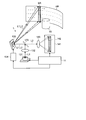
- FIG. 2 is a diagram for explaining an optical system of the ToF sensor according to the present embodiment. 2 illustrates a so-called scan type optical system that horizontally scans the angle of view of the light receiving unit 14, but the present invention is not limited to this, and for example, a so-called fixed angle of view of the light receiving unit 14 may be used. It is also possible to use a flash type ToF sensor.
- the ToF sensor 1 includes a light source 131, a collimator lens 132, a half mirror 133, a galvano mirror 135, a light receiving lens 146, and a SPAD array 141 as an optical system.
- the light source 131, the collimator lens 132, the half mirror 133, and the galvano mirror 135 are included in the light emitting unit 13 in FIG. 1, for example.
- the light receiving lens 146 and the SPAD array 141 are included in the light receiving unit 14 in FIG. 1, for example.
- the laser light L1 emitted from the light source 131 is converted by the collimator lens 132 into rectangular parallel light whose cross-section intensity spectrum is long in the vertical direction, and then enters the half mirror 133.
- the half mirror 133 reflects a part of the incident laser beam L1.
- the laser light L1 reflected by the half mirror 133 enters the galvano mirror 135.
- the galvanometer mirror 135 vibrates in the horizontal direction about a predetermined rotation axis as a vibration center by the driving unit 134 that operates under the control of the control unit 11, for example.
- the laser light L1 is horizontally scanned so that the angle of view SR of the laser light L1 reflected by the galvanometer mirror 135 reciprocally scans the range AR in the horizontal direction.
- a MEMS Micro Electro Mechanical System
- a micromotor or the like can be used for the drive unit 134.
- the laser beam L1 reflected by the galvanometer mirror 135 is reflected by the object 90 existing within the distance measuring range AR, and enters the galvanometer mirror 135 as reflected light L2.
- a part of the reflected light L2 incident on the galvano mirror 135 is transmitted through the half mirror 133 and incident on the light receiving lens 146, and thereby, an image is formed on a specific SPAD array 142 used in the SPAD array 141.
- the SPAD array 142 used may be the entire SPAD array 141 or a part thereof.
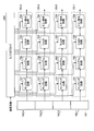
- FIG. 3 is a block diagram showing a schematic configuration example of the light receiving section according to the present embodiment.
- the light receiving unit 14 includes a SPAD array 141, a timing control circuit 143, a drive circuit 144, and an output circuit 145.
- the SPAD array 141 includes a plurality of SPAD pixels 20 arranged in a two-dimensional lattice.
- a pixel drive line LD vertical direction in the drawing
- an output signal line LS horizontal direction in the drawing
- One end of the pixel drive line LD is connected to the output end corresponding to each column of the drive circuit 144
- one end of the output signal line LS is connected to the input end corresponding to each row of the output circuit 145.
- the reflected light L2 is detected by using all or part of the SPAD array 141.
- the area used in the SPAD array 141 (used SPAD array 142) is a rectangle that is long in the vertical direction and is the same as the image of the reflected light L2 formed on the SPAD array 141 when the entire laser light L1 is reflected as the reflected light L2. May be However, the present invention is not limited to this, and may be variously modified such as a region larger or smaller than the image of the reflected light L2 formed on the SPAD array 141.
- the drive circuit 144 includes a shift register, an address decoder, and the like, and drives each SPAD pixel 20 of the SPAD array 141 simultaneously with all pixels or in units of columns. Therefore, the drive circuit 144 at least applies a quench voltage V_QCH described later to each SPAD pixel 20 in the selected column in the SPAD array 141 and a selection control voltage V_SEL described below to each SPAD pixel 20 in the selected column. And a circuit for applying the voltage. Then, the drive circuit 144 applies the selection control voltage V_SEL to the pixel drive line LD corresponding to the column to be read, thereby selecting the SPAD pixel 20 used for detecting the incidence of photons in column units.
- a signal (referred to as a detection signal) V_OUT output from each SPAD pixel 20 in the column selectively scanned by the drive circuit 144 is input to the output circuit 145 through each output signal line LS.
- the output circuit 145 outputs the detection signal V_OUT input from each SPAD pixel 20 to the SPAD adder 40 provided for each macro pixel described later.
- the timing control circuit 143 includes a timing generator that generates various timing signals, and controls the drive circuit 144 and the output circuit 145 based on the various timing signals generated by the timing generator.
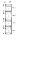
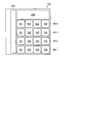
- FIG. 4 is a schematic diagram showing a schematic configuration example of the used SPAD array according to the present embodiment.
- the used SPAD array 142 has, for example, a configuration in which a plurality of SPAD pixels 20 are arranged in a two-dimensional lattice.
- the plurality of SPAD pixels 20 are grouped into a plurality of macro pixels 30 each including a predetermined number of SPAD pixels 20 arranged in the row and/or column direction.
- the shape of the region connecting the outer edges of the SPAD pixels 20 located on the outermost periphery of each macro pixel 30 has a predetermined shape (for example, a rectangle).
- the used SPAD array 142 is composed of, for example, a plurality of macro pixels 30 arranged in the vertical direction (corresponding to the column direction).
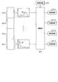
- the used SPAD array 142 is divided into, for example, a plurality of areas (hereinafter referred to as SPAD areas) in the vertical direction.
- the used SPAD array 142 is divided into four SPAD areas 142-1 to 142-4.
- the SPAD region 142-1 located at the bottom corresponds to, for example, the bottom 1 ⁇ 4 region in the view angle SR of the used SPAD array 142, and the SPAD region 142-2 above it is at the view angle SR, for example.
- the second 1/4 region from the bottom corresponds to the SPAD region 142-3 above the third quarter region from the bottom in the angle of view SR, and the uppermost SPAD region 142-4 corresponds to the third quarter from the bottom. , For example, corresponds to the uppermost 1 ⁇ 4 area in the angle of view SR.
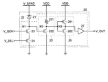
- FIG. 5 is a circuit diagram showing a schematic configuration example of the SPAD pixel according to the present embodiment.
- the SPAD pixel 20 includes a photodiode 21 as a light receiving element, and a readout circuit 22 that detects that a photon is incident on the photodiode 21.
- the photodiode 21 generates an avalanche current when a photon is incident while a reverse bias voltage V_SPAD of a breakdown voltage (breakdown voltage) or more is applied between its anode and cathode.
- the read circuit 22 includes a quench resistor 23, a digital converter 25, an inverter 26, a buffer 27, and a selection transistor 24.
- the quench resistor 23 is composed of, for example, an N-type MOSFET (Metal Oxide Semiconductor Field Effect Transistor; hereinafter referred to as an NMOS transistor), its drain is connected to the anode of the photodiode 21, and its source is connected via the selection transistor 24. It is grounded. Further, the quench voltage V_QCH preset for causing the NMOS transistor to act as a quench resistor is applied to the gate of the NMOS transistor forming the quench resistor 23 from the drive circuit 144 via the pixel drive line LD. ..
- the photodiode 21 is a SPAD.
- the SPAD is an avalanche photodiode that operates in the Geiger mode when a reverse bias voltage equal to or higher than the breakdown voltage (breakdown voltage) is applied between its anode and cathode, and can detect the incidence of one photon.
- the digital converter 25 includes a resistor 251 and an NMOS transistor 252.
- the NMOS transistor 252 has its drain connected to the power supply voltage VDD via the resistor 251, and its source grounded.
- the voltage of the connection point N1 between the anode of the photodiode 21 and the quench resistor 23 is applied to the gate of the NMOS transistor 252.
- the inverter 26 includes a P-type MOSFET (hereinafter referred to as a PMOS transistor) 261 and an NMOS transistor 262.
- the PMOS transistor 261 has its drain connected to the power supply voltage VDD and its source connected to the drain of the NMOS transistor 262.
- the NMOS transistor 262 has its drain connected to the source of the PMOS transistor 261, and its source grounded.
- the voltage of the connection point N2 between the resistor 251 and the drain of the NMOS transistor 252 is applied to the gate of the PMOS transistor 261 and the gate of the NMOS transistor 262, respectively.
- the output of the inverter 26 is input to the buffer 27.
- the buffer 27 is a circuit for impedance conversion, and when an output signal is input from the inverter 26, the input output signal is impedance-converted and output as a detection signal V_OUT.
- the selection transistor 24 is, for example, an NMOS transistor, the drain of which is connected to the source of the NMOS transistor that constitutes the quench resistor 23, and the source of which is grounded.
- the selection transistor 24 is connected to the drive circuit 144, and when the selection control voltage V_SEL from the drive circuit 144 is applied to the gate of the selection transistor 24 via the pixel drive line LD, the off state is changed to the on state. ..
- the readout circuit 22 illustrated in FIG. 5 operates as follows, for example. That is, first, while the selection control voltage V_SEL is applied from the drive circuit 144 to the selection transistor 24 and the selection transistor 24 is in the ON state, the photodiode 21 has a reverse bias voltage V_SPAD equal to or higher than the breakdown voltage (breakdown voltage). Is applied. As a result, the operation of the photodiode 21 is permitted.
- the selection control voltage V_SEL is not applied from the drive circuit 144 to the selection transistor 24 and the reverse bias voltage V_SPAD is not applied to the photodiode 21 while the selection transistor 24 is in the off state, the photodiode 21 Is prohibited.
- the high-level detection signal V_OUT is output from the buffer 27.
- the voltage applied between the anode and the cathode of the photodiode 21 becomes smaller than the breakdown voltage, whereby the avalanche current stops and the voltage at the connection point N1 is stopped.
- the NMOS transistor 452 is turned off and the output of the detection signal V_OUT from the buffer 27 is stopped (low level).
- the avalanche current is stopped and the NMOS transistor 452 is turned off from the timing when the photon is incident on the photodiode 21 and the avalanche current is generated and the NMOS transistor 452 is turned on.
- the high-level detection signal V_OUT is output for the period up to the timing.
- the output detection signal V_OUT is input to the SPAD adder 40 for each macro pixel 30 via the output circuit 145. Therefore, the detection signal V_OUT of the number (the number of detections) of the SPAD pixels 20 in which the incidence of photons is detected among the plurality of SPAD pixels 20 configuring one macro pixel 30 is input to each SPAD addition unit 40. ..
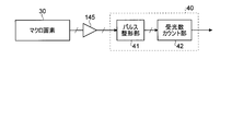
- FIG. 6 is a block diagram showing a more detailed configuration example of the SPAD adder according to the present embodiment.
- the SPAD addition unit 40 may be included in the light receiving unit 14 or may be included in the calculation unit 15.
- the SPAD addition unit 40 includes, for example, a pulse shaping unit 41 and a received light number counting unit 42.
- the pulse shaping unit 41 shapes the pulse waveform of the detection signal V_OUT input from the SPAD array 141 via the output circuit 145 into a pulse waveform having a time width according to the operation clock of the SPAD addition unit 40.
- the received light number counting unit 42 counts the detection signal V_OUT input from the corresponding macro pixel 30 in each sampling period, thereby determining the number (detection number) of the SPAD pixels 20 in which photon incidence is detected in each sampling period. It counts and outputs this count value as the pixel value of the macro pixel 30.
- the sampling cycle is a cycle for measuring the time (flying time) from when the light emitting unit 13 emits the laser light L1 to when the light receiving unit 14 detects the incidence of photons.
- the sampling cycle is set to a cycle shorter than the light emission cycle of the light emitting unit 13. For example, by shortening the sampling cycle, it is possible to calculate the flight time of photons emitted from the light emitting unit 13 and reflected by the object 90 with higher time resolution. This means that by increasing the sampling frequency, it is possible to calculate the distance to the object 90 with higher distance measurement resolution.
- the speed of light C is constant ( Since C ⁇ 300,000,000 m (meter)/s (second), the distance L to the object 90 can be calculated by the following equation (1).
- L C ⁇ t/2 (1)
- the sampling cycle will be 1 ns (nanosecond). In that case, one sampling period corresponds to 15 cm (centimeter). This indicates that the distance measurement resolution is 15 cm when the sampling frequency is 1 GHz.
- the sampling frequency is doubled to 2 GHz, the sampling period is 0.5 ns (nanosecond), and thus one sampling period corresponds to 7.5 cm (centimeter). This indicates that the distance measurement resolution can be halved when the sampling frequency is doubled. In this way, by increasing the sampling frequency and shortening the sampling cycle, it is possible to calculate the distance to the object 90 more accurately.
- FIG. 7 is a diagram showing an example of the depth image acquired by the ToF sensor according to the present embodiment, and is the depth acquired by the ToF sensor 1 installed in a state of facing the front of the vehicle. It is a figure which shows an example of an image.
- the depth image 50 corresponding to the distance measuring range AR is the depth to the object existing in the distance measuring range AR. It is acquired as information. Therefore, as illustrated in FIG. 4, when the vertically long SPAD array 142 is vertically divided into four, the depth image 50 can be divided into four regions 50-1 to 50-4 arranged in the vertical direction. ..
- the first area 50-1 is the depth image acquired in the SPAD area 142-1 and the second area 50-2 is the depth image acquired in the SPAD area 142-2.
- -3 is a depth image acquired in the SPAD area 142-3, and a fourth area 50-4 is a depth image acquired in the SPAD area 142-4.
- the first region 50-1 located at the bottom is, for example, a depth image near the foot of a vehicle equipped with the ToF sensor 1. Therefore, it is highly possible that the first region 50-1 includes an object existing at a short distance from the vehicle, such as a road surface, a white line, or a curb.
- the fourth region 50-4 located at the top is, for example, a depth image near the upper part of the vehicle. Therefore, there is a high possibility that the fourth region 50-4 includes an object existing at a long distance from the vehicle, such as a sign or a signboard.
- the second area 50-2 is, for example, a depth image in the lower front of the vehicle. Therefore, it is highly possible that the second region 50-2 includes an object at an intermediate distance between a short distance and a long distance, such as a preceding vehicle between roads or a road surface.
- the third region 50-3 is, for example, a depth image in the front upper part of the vehicle. Therefore, the third area 50-3 is an intermediate distance between a short distance and a long distance, such as an open leading vehicle between vehicles or a road work such as a traffic signal, and is included in the second area 50-2. It is more likely that an object that exists at a longer distance is included than an object that has a high probability.
- the horizontal line H1 may be included in the second area 50-2 or the third area 50-3. Further, without being limited to these, it may be included in the first or fourth region 50-1 or 50-4, or may not be included in any of the regions 50-1 to 50-4.
- the emission of the laser beam L1 for obtaining the depth image of a certain region (angle of view) once or a plurality of times corresponds to the angle of view of the SPAD array 142 used, which is indicated by the broken line in FIG. A frame image of the area to be processed is acquired. Therefore, in the case where the used SPAD array 142 is divided into four in the vertical direction, the SPAD area 142-1 of the SPAD area 142-1 is emitted with respect to one or a plurality of times of emission of the laser light L1 for acquiring the depth image of a certain area (angle of view).
- a frame image 51-4 corresponding to the angle of view of 142-4 is acquired.
- the frame images 51-1 to 51-4 slide in the horizontal direction as the laser light L1 is scanned in the horizontal direction.
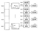
- the arithmetic unit 15 is arranged so as to be one-to-one with respect to each of the four SPAD areas 142-1 to 142-4. It is divided into one calculation unit 15-1 to 15-4, and individual calculation coefficients 16-1 to 16-4 are set for each calculation unit 15-1 to 15-4.
- the arithmetic coefficient 16-1 is used to extract the component of the reflected light L2 from the detected light.
- a high threshold value Sth1 (see FIG. 8) is set as a threshold value, and a filter coefficient for removing low-frequency noise components is set, while the calculation unit 15-corresponding to the SPAD area 142-4 in which an object easily exists at a long distance.
- a low threshold value Sth4 (see FIG. 9) as a calculation coefficient 16-4 and a filter coefficient for removing a high frequency noise component.
- the optimum calculation coefficient 16-2 is determined according to the distance to the object predicted in each of the second area 50-2 and the third area 50-3. And 16-3 can be set.
- calculation coefficients 16-1 to 16-4 set in the calculation units 15-1 to 15-4 according to the present embodiment have been described above, for example, as illustrated in FIG.
- a threshold value hereinafter, referred to as an echo threshold value
- a filter coefficient hereinafter, simply referred to as a filter coefficient
- Image resolution hereinafter, simply referred to as resolution
- frame rate hereinafter, simply referred to as frame rate
- histogram output range time zone
- histogram output range It can be illustrated.
- the echo threshold is a threshold for extracting the component of the reflected light L2 from the light detected by the SPAD pixel 20, and as illustrated in FIG. 12, for example, an object may exist at a short distance.
- the value may be set to a higher value in the first area 50-1 having a higher possibility and a lower value in the fourth area 50-4 in which an object is more likely to exist at a long distance.
- the filter coefficient is a filter coefficient for removing a noise component from the created histogram, and as illustrated in FIG. 12, for example, a filter that cuts low frequency components in the first region 50-1 A coefficient may be set, and a filter coefficient that cuts high frequency components may be set in the fourth region 50-4.
- the resolution can be changed, for example, by changing the number of macro pixels 30 forming one pixel. As illustrated in FIG. 12, this resolution may be set to a higher value in the first area 50-1 and a lower value in the fourth area 50-4, for example.
- this resolution By lowering the resolution, it is possible to widen the dynamic range of one pixel, and it is possible to detect the weak reflected light L2 reflected by an object at a long distance.
- by increasing the resolution it is possible to acquire a finer depth image, so that it is possible to improve the ranging accuracy.
- the frame rate can be changed, for example, by changing the number of bins in the histogram created by the histogram circuit 152 described later and the light emission period of the light emitting unit 13.
- the frame rate can be doubled by halving the number of bins in the histogram and doubling the light emission period of the light emitting unit 13.
- the frame rate may be set to a value higher in the first area 50-1 and lower in the fourth area 50-4, for example.
- By increasing the frame rate it is possible to measure the distance to the object in a higher cycle, so that it becomes possible to quickly start the reaction to the object.
- by reducing the frame rate it is possible to reduce the amount of data processing, so that it is possible to achieve reduction in processing time and power consumption.
- the histogram output range can be changed, for example, by changing the output range (time zone) of the created histogram. For example, when calculating the distance to an object located at a short distance, the output band can be reduced by outputting the previous time zone in the histogram. On the other hand, when the distance to an object located at a long distance is calculated, the output band can be similarly reduced by outputting the subsequent time zone in the histogram. As illustrated in FIG. 12, the output range of the histogram may be, for example, the first region 50-1 as a previous time period in the histogram and the fourth region 50-4 as a later time period. By narrowing the output range of the histogram, it is possible to reduce the amount of data processing, so that it is possible to achieve reduction in processing time and power consumption.
- calculation coefficients are merely examples and various additions and changes are possible.
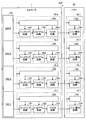
- FIG. 13 is a block diagram showing a schematic configuration example of the computing unit according to the present embodiment.
- each of the arithmetic units 15-1 to 15-4 includes a sampling circuit 151, a histogram circuit 152, a filter circuit 153, an echo detection circuit 154, and a register block 155.
- the register block 155 is, for example, a memory area configured by SRAM (Static Random Access Memory) or the like, and the calculation executed by each of the sampling circuit 151, the histogram circuit 152, the filter circuit 153, and the echo detection circuit 154 belonging to the same calculation unit. Stores individual calculation coefficients used in processing.
- SRAM Static Random Access Memory
- the sampling circuit 151 for example, according to the resolution of the calculation coefficients stored in the register block 155 of the same calculation unit, the detection signal for each macro pixel 30 output from the SPAD addition unit 40 in units of a predetermined number of macro pixels. By adding, the pixel value per pixel is calculated. This addition may be performed synchronously across the used SPAD array 142.
- the histogram circuit 152 uses, for example, a pixel value for each pixel calculated in synchronization by the sampling circuit 151 in accordance with the frame rate of the operation coefficients stored in the register block 155 of the same operation unit and/or the creation range of the histogram. Is added to the bin corresponding to the sampling period in the histogram of the pixel, in other words, the value of the bin corresponding to the flight time, to create a histogram for each pixel (see, for example, FIG. 8 or FIG. 9).
- the filter circuit 153 performs the filter process on the histogram created by the histogram circuit 152, for example, according to the noise-cut filter coefficient of the operation coefficients stored in the register block 155 of the same operation unit. Noise in the frequency band corresponding to the filter coefficient is removed.
- the echo detection circuit 154 extracts the component of the reflected light L2 from the noise-removed histogram according to the echo threshold value of the calculation coefficient stored in the register block 155 of the same calculation unit, and extracts the extracted reflected light L2.
- the distance to the object imaged in each pixel is calculated from the bin number (flight time) at which the cumulative pixel value reaches a peak.
- the frame images 51-1 to 51-4 configured by the distance to the object calculated as described above may be input to the host 80 via the control unit 11 or the external I/F 19, for example.
- the setting of calculation coefficients in the register blocks 155 of the calculation units 15-1 to 15-4 is performed, for example, as shown in FIG. It may be executed via the parameter setting units 156-1 to 156-4 provided for each of the four.
- the parameter setting units 156-1 to 156-4 may be a part of the control unit 11 or may be configured differently from the control unit 11.
- Each of the parameter setting units 156-1 to 156-4 stores, for example, the arithmetic coefficient designated by the host 80 in the register in each of the arithmetic units 15-1 to 15-4 based on the register address input together with the arithmetic coefficient.
- a broadcast parameter setting unit 156- common to the register blocks 155 in each of the arithmetic units 15-1 to 15-4. 5 may be provided apart from the parameter setting units 156-1 to 156-4.
- the broadcast parameter setting unit 156-5 stores the calculation coefficient instructed by the host 80 in the register block 155 in each of the calculation units 15-1 to 15-4 based on the register address input together with the calculation coefficient. May be stored.
- control unit 11 in the ToF sensor 1 inputs the arithmetic coefficient and the register address to each of the parameter setting units 156-1 to 156-4 or the broadcast parameter setting unit 156-5. It is also possible to
- the calculation coefficient input from the host 80 or the control unit 11 to each of the parameter setting units 156-1 to 156-4 or the broadcast parameter setting unit 156-5 may be set as a fixed value in advance, or the host 80.
- the control unit 11 may generate it based on a past frame image or the like, or the user may set the host 80 or the control unit 11.
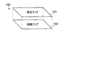
- FIG. 16 is a diagram showing an example of a laminated structure of the light-receiving unit and the calculation unit in the ToF sensor according to this embodiment.
- the light receiving unit 14 and the arithmetic unit 15 have a structure of a bonded chip 100 in which a light receiving chip 101 and a circuit chip 102 are bonded to each other in the vertical direction.
- the light receiving chip 101 is, for example, a semiconductor chip including a SPAD array 141 in which the photodiodes 21 in the SPAD pixels 20 of the light receiving unit 14 are arranged, and the circuit chip 102 is other than the photodiodes 21 of the SPAD pixels 20 in the light receiving unit 14, for example. And a semiconductor chip in which the arithmetic unit 15 in FIG. 1 is arranged.
- so-called direct joining can be used, in which the respective joining surfaces are flattened and the two are stuck together by an electron force.
- the present invention is not limited to this, and for example, so-called Cu-Cu bonding, in which electrode pads made of copper (Cu) formed on the bonding surfaces of each other are bonded, or other bump bonding may be used. ..
- the light receiving chip 101 and the circuit chip 102 are electrically connected to each other, for example, through a connecting portion such as a TSV (Through-Silicon Via) penetrating the semiconductor substrate.
- the connection using the TSV includes, for example, a so-called twin TSV system in which two TSVs, a TSV provided on the light receiving chip 101 and a TSV provided from the light receiving chip 101 to the circuit chip 102, are connected on the outside of the chip, or a light receiving method. It is possible to employ a so-called shared TSV system or the like in which both are connected by a TSV penetrating from the chip 101 to the circuit chip 102.
- the bonded chip 100 shown in FIG. 16 is not limited to the light receiving unit 14 and the arithmetic unit 15, and may include the light emitting unit 13, the control unit 11, and other units.
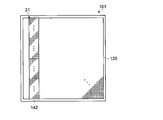
- FIG. 17 is a diagram showing an example of a plane layout of the light receiving surface of the light receiving chip 101.
- the effective pixel region 120 on the light receiving surface of the light receiving chip 101 has a configuration in which a plurality of photodiodes 21 are arranged in a two-dimensional lattice.
- the photodiodes 21 of the SPAD pixels 20 belonging to the used SPAD array 142 may be a part of the photodiodes 21 in the effective pixel area 120 or all the photodiodes 21.
- FIG. 18 is a diagram showing a planar layout example of the surface of the circuit chip 102 on the light receiving chip 101 side.
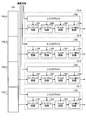
- a read circuit region 22A in which the read circuits 22 in the SPAD pixel 20 are arranged in a two-dimensional lattice is arranged in a region corresponding to the region of the used SPAD array 142 in the circuit chip 102.
- four arithmetic units 15-1 to 15-4 are arranged in parallel in a region adjacent to the read circuit region 22A.
- a sampling circuit 151 In each of the arithmetic units 15-1 to 15-4, a sampling circuit 151, a histogram circuit 152, a filter circuit 153, and an echo detection circuit 154 are arranged in order from a region near the read circuit region 22A.
- the detection signals output from the read circuit 22 By arranging the detection signals output from the read circuit 22 in this order in which the processes are executed, the wiring length from the read to the output can be shortened, so that signal delay and the like can be reduced. Is possible.
- a register block 155 is arranged in parallel with the arrangement of the sampling circuit 151, the histogram circuit 152, the filter circuit 153, and the echo detection circuit 154. In this way, by arranging the register block 155 so as to be close to the sampling circuit 151, the histogram circuit 152, the filter circuit 153, and the echo detection circuit 154, it is possible to route the signal line from the register block 155 to each circuit. It is possible to simplify.
- the circuit design of each operation unit is facilitated and the circuit pattern of each operation unit is Since it can be reused for the other four calculation units, there is an advantage that the time and effort required for circuit design can be significantly reduced.
- the angle of view of the SPAD array 142 used is divided into a plurality of regions (corresponding to the frame images 51-1 to 51-4), and each region is independent. Since it is possible to set the calculated calculation coefficient, it is possible to set the optimum calculation coefficient for each area according to the distance to the object that is likely to be copied in each area. As a result, it is possible to calculate the distance to the object by using the optimum calculation coefficient in each region. For example, when there are a short-distance object and a long-distance object in the distance measurement range AR. However, it is possible to reduce a decrease in distance measurement accuracy.
- calculation units 15-1 to 15-4 for each area can have the same circuit pattern, the time and effort required for circuit design can be significantly reduced.
- the present invention is not limited to this, and the longitudinal direction of the used SPAD array 142 is set to the horizontal direction and the used SPAD array 142 is used. It is possible to reciprocally scan the angle of view SR of in the vertical direction.
- the depth image 50 is divided into a plurality of areas 50-1 to 50-. It can be configured to be divided into four.
- each of the four divided operation units 15-1 to 15-4 includes the individual register block 155 (see FIG. 13 or FIG. 14) is illustrated.
- the second embodiment exemplifies a case where the register block is shared by a plurality of arithmetic units.
- FIG. 19 is a block diagram showing a schematic configuration example of the computing unit according to the present embodiment.
- the arithmetic unit 15 (see FIG. 1) is composed of four arithmetic units 25-1 to 25-4 and a shared register block 255.
- Each of the arithmetic units 25-1 to 25-4 includes a sampling circuit 151, a histogram circuit 152, a filter circuit 153, and an echo detection circuit 154, like the arithmetic units 15-1 to 15-4 according to the first embodiment. ..
- the register block 255 stores the calculation coefficients 16-1 to 16-4 corresponding to the regions 50-1 to 50-4 that the calculation units 25-1 to 25-4 are in charge of, and the calculation units 25-1 to 25- Appropriate calculation coefficients 16-1 to 16-4 are set for the sampling circuit 151, the histogram circuit 152, the filter circuit 153, and the echo detection circuit 154 in 25-4.
- FIG. 20 is a diagram showing an example of the plane layout of the surface of the circuit chip according to the present embodiment on the light receiving chip side.
- the circuit chip 102 according to this embodiment four arithmetic units 25-1 to 25-4 are arranged in parallel in a region adjacent to the read circuit region 22A.
- the register block 255 is arranged, for example, on the side adjacent to the area where the four arithmetic units 25-1 to 25-4 are arranged in the arrangement direction.
- the layout is not limited to this, and it is also possible to have a layout in which the register block 255 is arranged on the side opposite to the read circuit area 22A with the four arithmetic units 25-1 to 25-4 interposed therebetween.
- FIG. 21 is a block diagram showing a schematic configuration example of the computing unit according to the present embodiment.
- the arithmetic unit 15 (see FIG. 1) according to the present embodiment includes a sampling circuit 351, a histogram circuit 352, a filter circuit 353, and an echo shared by the four SPAD areas 142-1 to 142-4.
- the detection circuit 354 and the register blocks 155-1 to 155-4 storing the individual calculation coefficients 16-1 to 16-4 for the SPAD areas 142-1 to 142-4 are provided.
- a partial area in each of the sampling circuit 351, the histogram circuit 352, the filter circuit 353, and the echo detection circuit 354 and the register block 155-1 execute arithmetic processing on the signal read from the SPAD area 142-1.
- the arithmetic unit 35-1 is configured.
- a partial area in each of the sampling circuit 351, the histogram circuit 352, the filter circuit 353, and the echo detection circuit 354 and the register block 155-2 perform arithmetic processing on the signal read from the SPAD area 142-2.
- a part of the sampling circuit 351, the histogram circuit 352, the filter circuit 353, and the echo detection circuit 354 and the register block 155-3 are read from the SPAD area 142-3.
- An arithmetic unit 35-1 that executes arithmetic processing on the output signal is configured to include a partial area in each of the sampling circuit 351, the histogram circuit 352, the filter circuit 353, and the echo detection circuit 354 and the register block 155-4. Composes an arithmetic unit 35-1 for performing arithmetic processing on the signal read from the SPAD area 142-4.
- the operation coefficient 16-1 stored in the register block 155-1 is set in the area belonging to the operation unit 35-1 in the sampling circuit 351, the histogram circuit 352, the filter circuit 353, and the echo detection circuit 354.
- the regions belonging to the arithmetic units 35-2 to 35-4 in the sampling circuit 351, the histogram circuit 352, the filter circuit 353, and the echo detection circuit 354 are stored in the register blocks 155-2 to 155-4, respectively.
- the calculation coefficients 16-2 to 16-4 are set appropriately.
- FIG. 22 is a diagram showing an example of a planer layout of the surface of the circuit chip according to the present embodiment on the light receiving chip side.
- a shared sampling circuit 351, a histogram circuit 352, a filter circuit 353, and an echo detection circuit 354 are sequentially arranged in an area adjacent to the read circuit area 22A. .. Further, in the area opposite to the readout circuit area 22A with the sampling circuit 351, the histogram circuit 352, the filter circuit 353, and the echo detection circuit 354 in between, the register blocks 155-1 to 155-4 is arranged.
- the distance to the object can be calculated using the optimum calculation coefficient for each region, as in the first embodiment. Even when a short-distance object and a long-distance object exist within the distance range AR, it is possible to reduce deterioration of the distance measurement accuracy.
- the calculation unit 15 mounted on the ToF sensor 1 includes the sampling circuit 151, the histogram circuit 152, the filter circuit 153, the echo detection circuit 154, and the register block 155 is illustrated. However, it is possible to mount some of the sampling circuit 151, the histogram circuit 152, the filter circuit 153, and the echo detection circuit 154 in an external device such as the host 80.
- the histogram circuit 152, the filter circuit 153, the echo detection circuit 154, and the register in each of the calculation units 15-1 to 15-4 of the ToF sensor 1 are provided. It is also possible to mount a part of the block 155 on the host 80 and mount the sampling circuit 151 and its register block 155 on each of the arithmetic units 15-1 to 15-4 of the ToF sensor 1.
- the echo detection circuit 154 and its register block 155 in each of the arithmetic units 15-1 to 15-4 of the ToF sensor 1 are transferred to the host 80. It is also possible to mount the sampling circuit 151, the histogram circuit 152, the filter circuit 153, and the register block 155 in each of the arithmetic units 15-1 to 15-4 of the ToF sensor 1.
- the distance to the object can be calculated using the optimum calculation coefficient for each region, as in the first embodiment. Even when a short-distance object and a long-distance object exist within the distance range AR, it is possible to reduce deterioration of the distance measurement accuracy.
- the base embodiment is not limited to the first embodiment, and may be another embodiment. ..
- FIG. 26 is a block diagram showing a schematic configuration example of the vehicle-mounted system according to the present embodiment.
- the in-vehicle system 500 includes, for example, a ToF sensor 1, an automatic driving module 501, and an ECU (Engine Control Unit) 502.
- the ECU 502 includes, for example, a CPU (Central Processing Unit), a ROM (Read Only Memory), a RAM (Random Access Memory), a display control unit, a voice control unit, an SSD (Solid State Drive, flash memory), etc. It executes various controls related to the running of the vehicle and the environment inside the vehicle. Further, the ECU 502 notifies the automatic driving module 501 of various kinds of information regarding the traveling of the vehicle, the environment inside the vehicle, and the like.
- a CPU Central Processing Unit
- ROM Read Only Memory
- RAM Random Access Memory
- a display control unit a voice control unit
- SSD Solid State Drive, flash memory
- the automatic driving module 501 executes various processes for automatically controlling the traveling of the vehicle based on the distance measurement result from the ToF sensor 1 based on various information regarding the traveling of the vehicle, the environment inside the vehicle, and the like notified from the ECU 502. To do.
- the automatic driving module 501 based on various information about the running of the vehicle, the environment inside the vehicle, and the like notified from the ECU 502, sets the calculation coefficients 16-1 to 16-4 to be set in the calculation units 15-1 to 15-4 of the ToF sensor 1. 16-4 is input to the ToF sensor 1.
- the automatic operation module 501 corresponds to, for example, the host 80 in the above-described embodiment.
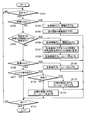
- FIG. 27 is a flowchart showing a schematic example of the operation coefficient switching operation according to the present embodiment.
- the automatic driving module 501 determines whether or not the vehicle is traveling in accordance with the information provided from the ECU 502 (step S101), and the vehicle starts traveling. It stands by until it does (NO in step S101).
- the automatic driving module 501 When the vehicle starts running (YES in step S101), the automatic driving module 501 first determines whether or not the current illuminance S outside the vehicle detected by an illuminance sensor or the like (not shown) is equal to or less than the illuminance threshold S1. (Step S102). When the illuminance S is larger than the illuminance threshold S1 (NO in step S102), the automatic driving module 501 proceeds to step S105. On the other hand, when the illuminance S is equal to or less than the illuminance threshold S1 (YES in step S102), the automatic driving module 501 calculates to lower the echo thresholds for all the regions of the first region 50-1 to the fourth region 50-4. While changing the coefficients 16-1 to 16-4 (step S103), for example, the calculation coefficient 16-4 is changed so as to increase the resolution of the fourth region 50-4 (step S104), and then the process proceeds to step S115. ..
- step S102 instead of comparing the current illuminance S and the illuminance threshold S1, for example, it may be determined whether or not it is a specific time zone (mainly at night). Further, the reduction range of the echo threshold value in step S103 may be set in advance or may be a reduction range according to the current illuminance S. Further, the resolution reduction amount in step S104 may be set in advance or may be a reduction amount according to the current illuminance S. Furthermore, the area in which the resolution is lowered in step S104 is not limited to the fourth area 50-4, and various additions and changes such as the third area 50-3 can be made.
- step S105 the automatic driving module 501 determines that the distance D from the vehicle or the ToF sensor 1 to the object existing in the distance measuring area AR of the ToF sensor 1 in the first area 50-1 to the fourth area 50-4. It is determined whether or not there is a region with a distance threshold D1 or less. When there is no area where the distance D is equal to or less than the distance threshold D1 (NO in step S105), the automatic driving module 501 proceeds to step S109. On the other hand, when there is a region in which the distance D is equal to or less than the distance threshold D1 (YES in step S105), the automatic driving module 501 increases the echo threshold in the corresponding region (step S106) and sets the filter coefficient of the corresponding region as well. While changing to the filter coefficient for low frequency removal (step S107), the frame rate of the corresponding region is increased (step S108), and then the process proceeds to step S115.
- the distance D to the object may be calculated based on an image acquired by an image sensor (not shown) or the like, not limited to the previous frame acquired by the ToF sensor 1.
- the increment of the echo threshold value in step S106 may be set in advance or may be the increment according to the current distance D.
- the frequency band to be removed after the change may be a preset frequency band or a frequency band according to the current distance D.
- the increment of the frame rate in step S108, the increment of the echo threshold in step S106 may be set in advance, or may be the increment according to the current distance D.
- step S109 the automatic driving module 501 determines whether the current vehicle speed V is equal to or higher than the speed threshold V1 according to the information provided from the ECU 502. When the vehicle speed V is less than the speed threshold V1 (NO in step S109), the automatic driving module 501 proceeds to step S111. On the other hand, when the vehicle speed V is equal to or higher than the speed threshold V1 (YES in step S109), the automatic driving module 501 increases the frame rate of all areas (step S110), and then proceeds to step S115.
- the increment of the frame rate in step S110 and the increment of the echo threshold in step S106 may be set in advance, or may be the increment according to the current vehicle speed V.
- step S111 the automatic driving module 501 determines whether or not a handle having a predetermined turning angle or more is operated manually or automatically according to the information provided from the ECU 502. When the steering wheel operation is not performed at a certain turning angle or more (NO in step S111), the automatic driving module 501 proceeds to step S115. On the other hand, when the steering wheel operation is performed at a certain turning angle or more (YES in step S111), the automatic driving module 501 determines whether the vehicle turns right based on the operation amount of the steering wheel (step S112). When the vehicle turns right (YES in step S112), the automatic driving module 501 increases the frame rate for the right area of the distance measurement area AR (step S113), and then proceeds to step S115.
- the automatic driving module 501 increases the frame rate for the left area of the distance measurement area AR (step S114), and then proceeds to step S115. ..
- step S115 the automatic driving module 501 determines whether or not to end this operation, for example, according to an instruction from the ECU 502, and if it ends (YES in step S115), ends this operation. On the other hand, when not ending (NO in step S115), the automatic driving module 501 returns to step S101 and continuously executes the subsequent operations.
- the technology according to the present disclosure can be applied to various products.
- the technology according to the present disclosure is applicable to any type of movement such as an automobile, an electric vehicle, a hybrid electric vehicle, a motorcycle, a bicycle, a personal mobility, an airplane, a drone, a ship, a robot, a construction machine, and an agricultural machine (tractor). It may be realized as a device mounted on the body.
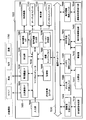
- FIG. 28 is a block diagram showing a schematic configuration example of a vehicle control system 7000 which is an example of a mobile body control system to which the technology according to the present disclosure can be applied.
- the vehicle control system 7000 includes a plurality of electronic control units connected via a communication network 7010.
- the vehicle control system 7000 includes a drive system control unit 7100, a body system control unit 7200, a battery control unit 7300, a vehicle exterior information detection unit 7400, a vehicle interior information detection unit 7500, and an integrated control unit 7600. ..
- the communication network 7010 connecting these plural control units complies with any standard such as CAN (Controller Area Network), LIN (Local Interconnect Network), LAN (Local Area Network) or FlexRay (registered trademark). It may be an in-vehicle communication network.
- CAN Controller Area Network
- LIN Local Interconnect Network
- LAN Local Area Network
- FlexRay registered trademark
- Each control unit includes a microcomputer that performs arithmetic processing according to various programs, a storage unit that stores a program executed by the microcomputer or parameters used in various arithmetic operations, and a drive circuit that drives various controlled devices. Equipped with.
- Each control unit is equipped with a network I/F for communicating with other control units via the communication network 7010, and also by wire communication or wireless communication with devices or sensors inside or outside the vehicle. A communication I/F for performing communication is provided. In FIG.
- a microcomputer 7610 As the functional configuration of the integrated control unit 7600, a microcomputer 7610, a general-purpose communication I/F 7620, a dedicated communication I/F 7630, a positioning unit 7640, a beacon receiving unit 7650, an in-vehicle device I/F 7660, an audio image output unit 7670, An in-vehicle network I/F 7680 and a storage unit 7690 are illustrated.
- the other control units also include a microcomputer, a communication I/F, a storage unit, and the like.
- the drive system control unit 7100 controls the operation of devices related to the drive system of the vehicle according to various programs.
- the drive system control unit 7100 includes a drive force generation device for generating a drive force of a vehicle such as an internal combustion engine or a drive motor, a drive force transmission mechanism for transmitting the drive force to wheels, and a steering angle of the vehicle. It functions as a steering mechanism for adjusting and a control device such as a braking device for generating a braking force of the vehicle.
- the drive system control unit 7100 may have a function as a control device such as ABS (Antilock Brake System) or ESC (Electronic Stability Control).
- a vehicle state detection unit 7110 is connected to the drive system control unit 7100.
- the vehicle state detection unit 7110 includes, for example, a gyro sensor that detects the angular velocity of the shaft rotational movement of the vehicle body, an acceleration sensor that detects the acceleration of the vehicle, an accelerator pedal operation amount, a brake pedal operation amount, or a steering wheel steering operation. At least one of sensors for detecting an angle, an engine speed, a wheel rotation speed, and the like is included.
- the drive system control unit 7100 performs arithmetic processing using the signal input from the vehicle state detection unit 7110 to control the internal combustion engine, drive motor, electric power steering device, brake device, or the like.
- the body system control unit 7200 controls the operation of various devices mounted on the vehicle body according to various programs.
- the body system control unit 7200 functions as a keyless entry system, a smart key system, a power window device, or a control device for various lamps such as a head lamp, a back lamp, a brake lamp, a winker, or a fog lamp.
- the body system control unit 7200 may receive radio waves or signals of various switches transmitted from a portable device that substitutes for a key.
- the body system control unit 7200 receives the input of these radio waves or signals and controls the vehicle door lock device, the power window device, the lamp, and the like.
- the battery control unit 7300 controls the secondary battery 7310 that is the power supply source of the drive motor according to various programs. For example, to the battery control unit 7300, information such as the battery temperature, the battery output voltage, or the remaining capacity of the battery is input from the battery device including the secondary battery 7310. The battery control unit 7300 performs arithmetic processing using these signals to control the temperature adjustment of the secondary battery 7310 or the cooling device provided in the battery device.
- the exterior information detection unit 7400 detects information outside the vehicle equipped with the vehicle control system 7000.
- the image capturing unit 7410 and the vehicle exterior information detection unit 7420 is connected to the vehicle exterior information detection unit 7400.
- the imaging unit 7410 includes at least one of a ToF (Time Of Flight) camera, a stereo camera, a monocular camera, an infrared camera, and other cameras.
- the outside-vehicle information detection unit 7420 detects, for example, an environment sensor for detecting current weather or weather, or another vehicle around the vehicle equipped with the vehicle control system 7000, an obstacle, a pedestrian, or the like. At least one of the ambient information detection sensors of.
- the environmental sensor may be, for example, at least one of a raindrop sensor that detects rainy weather, a fog sensor that detects fog, a sunshine sensor that detects the degree of sunshine, and a snow sensor that detects snowfall.
- the ambient information detection sensor may be at least one of an ultrasonic sensor, a radar device, and a LIDAR (Light Detection and Ranging, Laser Imaging Detection and Ranging) device.
- the imaging unit 7410 and the vehicle exterior information detection unit 7420 may be provided as independent sensors or devices, or may be provided as a device in which a plurality of sensors or devices are integrated.
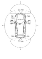
- FIG. 29 shows an example of installation positions of the imaging unit 7410 and the vehicle exterior information detection unit 7420.
- the imaging units 7910, 7912, 7914, 7916, 7918 are provided at at least one of the front nose of the vehicle 7900, the side mirrors, the rear bumper, the back door, and the upper part of the windshield inside the vehicle.
- the image capturing unit 7910 provided on the front nose and the image capturing unit 7918 provided on the upper part of the windshield in the vehicle interior mainly acquire an image in front of the vehicle 7900.
- the imaging units 7912 and 7914 provided in the side mirrors mainly acquire images of the side of the vehicle 7900.
- the imaging unit 7916 provided on the rear bumper or the back door mainly acquires an image of the rear of the vehicle 7900.
- the imaging unit 7918 provided on the upper part of the windshield in the vehicle interior is mainly used for detecting a preceding vehicle, a pedestrian, an obstacle, a traffic signal, a traffic sign, a lane, or the like.
- FIG. 29 shows an example of the shooting ranges of the respective image pickup units 7910, 7912, 7914, 7916.
- the imaging range a indicates the imaging range of the imaging unit 7910 provided on the front nose
- the imaging ranges b and c indicate the imaging ranges of the imaging units 7912 and 7914 provided on the side mirrors
- the imaging range d is The imaging range of the imaging part 7916 provided in the rear bumper or the back door is shown.
- a bird's-eye view image of the vehicle 7900 viewed from above can be obtained.
- the vehicle exterior information detection units 7920, 7922, 7924, 7926, 7928, 7930 provided on the front, rear, sides, corners of the vehicle 7900 and on the windshield inside the vehicle may be ultrasonic sensors or radar devices, for example.
- the vehicle exterior information detection units 7920, 7926, 7930 provided on the front nose, rear bumper, back door, and upper windshield of the vehicle 7900 may be LIDAR devices, for example.
- These vehicle exterior information detection units 7920 to 7930 are mainly used to detect a preceding vehicle, a pedestrian, an obstacle, or the like.
- the vehicle exterior information detection unit 7400 causes the image capturing unit 7410 to capture an image of the vehicle exterior and receives the captured image data.
- the vehicle exterior information detection unit 7400 receives detection information from the vehicle exterior information detection unit 7420 connected thereto.
- the vehicle exterior information detection unit 7420 is an ultrasonic sensor, a radar device, or a LIDAR device
- the vehicle exterior information detection unit 7400 transmits ultrasonic waves, electromagnetic waves, or the like, and receives information on the received reflected waves.
- the vehicle exterior information detection unit 7400 may perform an object detection process or a distance detection process such as a person, a car, an obstacle, a sign, or characters on the road surface based on the received information.
- the vehicle exterior information detection unit 7400 may perform environment recognition processing for recognizing rainfall, fog, road surface conditions, or the like based on the received information.
- the vehicle exterior information detection unit 7400 may calculate the distance to an object outside the vehicle based on the received information.
- the vehicle exterior information detection unit 7400 may also perform image recognition processing or distance detection processing for recognizing a person, a car, an obstacle, a sign, characters on the road surface, or the like based on the received image data.
- the vehicle exterior information detection unit 7400 performs processing such as distortion correction or position adjustment on the received image data, combines the image data captured by different image capturing units 7410, and generates an overhead image or a panoramic image. Good.
- the vehicle exterior information detection unit 7400 may perform viewpoint conversion processing using image data captured by different image capturing units 7410.
- the in-vehicle information detection unit 7500 detects in-vehicle information.
- the in-vehicle information detection unit 7500 is connected with, for example, a driver state detection unit 7510 that detects the state of the driver.
- the driver state detecting unit 7510 may include a camera for capturing an image of the driver, a biometric sensor for detecting biometric information of the driver, a microphone for collecting voice in the vehicle interior, or the like.
- the biometric sensor is provided on, for example, a seat surface or a steering wheel, and detects biometric information of an occupant sitting on a seat or a driver who holds the steering wheel.
- the in-vehicle information detection unit 7500 may calculate the degree of fatigue or concentration of the driver based on the detection information input from the driver state detection unit 7510, or determine whether the driver is asleep. You may.
- the in-vehicle information detection unit 7500 may perform processing such as noise canceling processing on the collected audio signal.
- the integrated control unit 7600 controls overall operations in the vehicle control system 7000 according to various programs.
- An input unit 7800 is connected to the integrated control unit 7600.
- the input unit 7800 is realized by a device that can be input and operated by a passenger, such as a touch panel, a button, a microphone, a switch or a lever. Data obtained by voice recognition of voice input by a microphone may be input to the integrated control unit 7600.
- the input unit 7800 may be, for example, a remote control device that uses infrared rays or other radio waves, or may be an external connection device such as a mobile phone or a PDA (Personal Digital Assistant) that supports the operation of the vehicle control system 7000. May be.
- the input unit 7800 may be, for example, a camera, in which case the passenger can input information by gesture. Alternatively, data obtained by detecting the movement of the wearable device worn by the passenger may be input. Furthermore, the input unit 7800 may include, for example, an input control circuit that generates an input signal based on information input by a passenger or the like using the input unit 7800 and outputs the input signal to the integrated control unit 7600. A passenger or the like operates the input unit 7800 to input various data or instruct a processing operation to the vehicle control system 7000.
- the storage unit 7690 may include a ROM (Read Only Memory) that stores various programs executed by the microcomputer, and a RAM (Random Access Memory) that stores various parameters, calculation results, sensor values, and the like.
- the storage unit 7690 may be realized by a magnetic storage device such as an HDD (Hard Disc Drive), a semiconductor storage device, an optical storage device, a magneto-optical storage device, or the like.
- the general-purpose communication I/F 7620 is a general-purpose communication I/F that mediates communication with various devices existing in the external environment 7750.
- the general-purpose communication I/F 7620 is a cellular communication protocol such as GSM (registered trademark) (Global System of Mobile communications), WiMAX (registered trademark), LTE (registered trademark) (Long Term Evolution), or LTE-A (LTE-Advanced).
- GSM Global System of Mobile communications
- WiMAX registered trademark
- LTE registered trademark
- LTE-A Long Term Evolution
- LTE-A Long Term Evolution-Advanced
- another wireless communication protocol such as a wireless LAN (also referred to as Wi-Fi (registered trademark)) or Bluetooth (registered trademark) may be implemented.
- the general-purpose communication I/F 7620 is connected to a device (for example, an application server or a control server) existing on an external network (for example, the Internet, a cloud network or a network unique to a business operator) via a base station or an access point, for example. You may.
- the general-purpose communication I/F 7620 uses, for example, P2P (Peer To Peer) technology, and is a terminal existing in the vicinity of the vehicle (for example, a driver, a pedestrian or a shop terminal, or an MTC (Machine Type Communication) terminal). May be connected with.
- P2P Peer To Peer
- MTC Machine Type Communication
- the dedicated communication I/F 7630 is a communication I/F that supports a communication protocol formulated for use in a vehicle.
- the dedicated communication I/F 7630 uses a standard protocol such as WAVE (Wireless Access in Vehicle Environment), DSRC (Dedicated Short Range Communications), or a cellular communication protocol, which is a combination of a lower layer IEEE 802.11p and an upper layer IEEE 1609, for example. May be implemented.
- the dedicated communication I/F 7630 is typically a vehicle-to-vehicle communication, a vehicle-to-infrastructure communication, a vehicle-to-home communication, and a vehicle-to-pedestrian communication. ) Perform V2X communications, a concept that includes one or more of the communications.
- the positioning unit 7640 receives, for example, a GNSS signal from a GNSS (Global Navigation Satellite System) satellite (for example, a GPS signal from a GPS (Global Positioning System) satellite) to perform positioning, and the latitude, longitude, and altitude of the vehicle. Generate position information including. Note that the positioning unit 7640 may specify the current position by exchanging signals with the wireless access point, or may acquire position information from a terminal such as a mobile phone, PHS, or smartphone having a positioning function.
- GNSS Global Navigation Satellite System
- GPS Global Positioning System
- the beacon receiving unit 7650 receives, for example, a radio wave or an electromagnetic wave transmitted from a wireless station or the like installed on the road, and acquires information such as the current position, traffic jam, traffic closure, or required time.
- the function of beacon reception unit 7650 may be included in dedicated communication I/F 7630 described above.
- the in-vehicle device I/F 7660 is a communication interface that mediates a connection between the microcomputer 7610 and various in-vehicle devices 7760 existing in the vehicle.
- the in-vehicle device I/F 7660 may establish a wireless connection using a wireless communication protocol such as wireless LAN, Bluetooth (registered trademark), NFC (Near Field Communication) or WUSB (Wireless USB).
- a wireless communication protocol such as wireless LAN, Bluetooth (registered trademark), NFC (Near Field Communication) or WUSB (Wireless USB).
- the in-vehicle device I/F 7660 is connected to a USB (Universal Serial Bus), HDMI (registered trademark) (High-Definition Multimedia Interface, or MHL (Mobile High) via a connection terminal (and a cable if necessary) not shown. -Definition Link) etc.
- the wired device 7760 may include, for example, at least one of a mobile device or a wearable device that the passenger has, or an information device that is carried in or attached to the vehicle. Further, the in-vehicle device 7760 may include a navigation device that searches for a route to an arbitrary destination.
- the in-vehicle device I/F 7660 is a control signal with the in-vehicle device 7760. Or exchange data signals.
- the in-vehicle network I/F 7680 is an interface that mediates communication between the microcomputer 7610 and the communication network 7010.
- the in-vehicle network I/F 7680 transmits and receives signals and the like according to a predetermined protocol supported by the communication network 7010.
- the microcomputer 7610 of the integrated control unit 7600 passes through at least one of the general-purpose communication I/F 7620, the dedicated communication I/F 7630, the positioning unit 7640, the beacon receiving unit 7650, the in-vehicle device I/F 7660, and the in-vehicle network I/F 7680.
- the vehicle control system 7000 is controlled according to various programs based on the information acquired by the above. For example, the microcomputer 7610 calculates a control target value of the driving force generation device, the steering mechanism or the braking device based on the acquired information on the inside and outside of the vehicle, and outputs a control command to the drive system control unit 7100. Good.
- the microcomputer 7610 realizes the functions of ADAS (Advanced Driver Assistance System) including collision avoidance or impact mitigation of a vehicle, follow-up traveling based on an inter-vehicle distance, vehicle speed maintenance traveling, vehicle collision warning, vehicle lane departure warning, etc. You may perform the coordinated control aiming at.
- the microcomputer 7610 controls the driving force generation device, the steering mechanism, the braking device, and the like based on the acquired information about the surroundings of the vehicle, so that the microcomputer 7610 automatically travels independently of the driver's operation. You may perform cooperative control for the purpose of driving etc.
- ADAS Advanced Driver Assistance System
- a general-purpose communication I/F 7620 a dedicated communication I/F 7630, a positioning unit 7640, a beacon receiving unit 7650, an in-vehicle device I/F 7660, and an in-vehicle network I/F 7680.
- the microcomputer 7610 may generate a warning signal by predicting a danger such as a vehicle collision, a pedestrian or the like approaching a road or a closed road, based on the acquired information.
- the warning signal may be, for example, a signal for generating a warning sound or lighting a warning lamp.
- the voice image output unit 7670 transmits an output signal of at least one of a voice and an image to an output device capable of visually or audibly notifying information to a passenger of the vehicle or the outside of the vehicle.
- an audio speaker 7710, a display unit 7720, and an instrument panel 7730 are illustrated as output devices.
- the display unit 7720 may include at least one of an onboard display and a head-up display, for example.
- the display unit 7720 may have an AR (Augmented Reality) display function.
- the output device may be a device other than these devices, such as headphones, a wearable device such as a glasses-type display worn by a passenger, a projector, or a lamp.
- the output device When the output device is a display device, the display device displays results obtained by various processes performed by the microcomputer 7610 or information received from another control unit in various formats such as text, images, tables, and graphs. Display it visually.
- the output device is an audio output device, the audio output device converts an audio signal composed of reproduced audio data, acoustic data, or the like into an analog signal and outputs it audibly.
- At least two control units connected via the communication network 7010 may be integrated as one control unit.
- each control unit may be composed of a plurality of control units.
- the vehicle control system 7000 may include another control unit not shown.
- some or all of the functions of one of the control units may be given to another control unit. That is, if the information is transmitted and received via the communication network 7010, the predetermined arithmetic processing may be performed by any of the control units.
- a sensor or device connected to one of the control units may be connected to another control unit, and a plurality of control units may send and receive detection information to and from each other via the communication network 7010. .
- the computer program for realizing each function of the ToF sensor 1 according to the present embodiment described with reference to FIG. 1 can be installed in any control unit or the like. It is also possible to provide a computer-readable recording medium in which such a computer program is stored.
- the recording medium is, for example, a magnetic disk, an optical disk, a magneto-optical disk, a flash memory, or the like. Further, the above computer program may be distributed, for example, via a network without using a recording medium.
- the ToF sensor 1 according to the present embodiment described with reference to FIG. 1 can be applied to the integrated control unit 7600 of the application example shown in FIG. 28.
- the control unit 11, the calculation unit 15, and the external I/F 19 of the ToF sensor 1 correspond to the microcomputer 7610, the storage unit 7690, and the vehicle-mounted network I/F 7680 of the integrated control unit 7600.
- the invention is not limited to this, and the vehicle control system 7000 may correspond to the host 80 in FIG. 1.
- the constituent elements of the ToF sensor 1 according to the present embodiment described with reference to FIG. 1 are modules for the integrated control unit 7600 shown in FIG. Circuit module).
- the ToF sensor 1 according to the present embodiment described with reference to FIG. 1 may be realized by a plurality of control units of the vehicle control system 7000 shown in FIG. 28.
- An array part in which a plurality of light receiving elements that detect the incidence of photons are arranged, A read circuit for reading a detection signal from each of the light receiving elements, A plurality of calculation units that generate depth information regarding a distance to an object existing within the angle of view of the region based on the detection signals read from the light receiving elements that belong to different regions in the array unit, Equipped with The distance measuring device in which the plurality of arithmetic units generate the depth information by using arithmetic coefficients at least partially different from each other.
- Each of the arithmetic units aggregates the number of the detection signals read out from each of the light receiving elements at a predetermined sampling cycle in a pixel unit including one or more of the light receiving elements, and thereby each pixel
- the distance measuring apparatus according to (1) further including a sampling circuit that generates the pixel value of.
- each of the arithmetic units further includes a histogram circuit that generates, for each pixel, a histogram of the pixel values for each of the sampling periods collected by the sampling circuit.
- each of the arithmetic units further includes a filter circuit that removes a noise component from the histogram for each pixel generated by the histogram circuit.
- each of the arithmetic units further includes an echo detection circuit that extracts a specific light component from the histogram from which the noise component has been removed by the filter circuit.
- Each of the operation coefficients is a threshold for the echo detection circuit to extract the specific light component from the histogram, a filter coefficient for the filter circuit to remove a noise component from the histogram, and the sampling circuit.
- the resolution includes at least one of a resolution for determining the number of the light receiving elements included in one pixel, a frame rate for reading the depth information from the array unit, and an output range indicating an output range in the histogram.
- the array unit includes a first region and a second region different from the first region, A plurality of calculation units that generate the depth information relating to a distance to an object existing within an angle of view of the first region based on the detection signal read from the light receiving element belonging to the first region; 1 operation unit and a second operation for generating the depth information related to the distance to an object existing within the angle of view of the second area based on the detection signal read from the light receiving element belonging to the second area Part and
- the calculation coefficient includes a threshold value for the echo detection circuit to extract the specific light component from the histogram, The distance measuring device according to (5), wherein the threshold value of the calculation coefficient set in the first calculation unit is a value higher than the threshold value of the calculation coefficient set in the second calculation unit.
- the array unit includes a first region and a second region different from the first region, A plurality of calculation units that generate the depth information relating to a distance to an object existing within an angle of view of the first region based on the detection signal read from the light receiving element belonging to the first region; 1 operation unit and a second operation for generating the depth information regarding the distance to an object existing within the angle of view of the second area based on the detection signal read from the light receiving element belonging to the second area Part and
- the operation coefficient includes a filter coefficient for the filter circuit to remove a noise component from the histogram,
- the filter coefficient in the calculation coefficient set in the first calculation unit is a filter coefficient that removes a frequency component lower than the filter coefficient in the calculation coefficient set in the second calculation unit.
- the array section is divided into a plurality of regions arranged in a line, The distance measuring device according to any one of (1) to (8), wherein each of the arithmetic units has a one-to-one correspondence with the region.
- each of the arithmetic units includes a register block that stores an individual arithmetic coefficient used when generating the depth information.
- (11) The distance measuring device according to any one of (1) to (9), further including a common register block that stores an individual calculation coefficient set for each of the calculation units.
- Each of the arithmetic units is The number of the detection signals read from each of the light receiving elements in a predetermined sampling cycle is aggregated in pixel units including one or more of the light receiving elements to generate a pixel value of each pixel in each sampling cycle.
- a sampling circuit A histogram circuit for generating, for each of the pixels, a histogram of the pixel values for each of the sampling periods collected by the sampling circuit;
- a filter circuit for removing a noise component from the histogram for each pixel generated by the histogram circuit;
- An echo detection circuit that extracts a specific light component from the histogram from which the noise component has been removed by the filter circuit, Including In each of the arithmetic units, the sampling circuit, the histogram circuit, the filter circuit, and the echo detection circuit are arranged in the order of the sampling circuit, the histogram circuit, the filter circuit, and the echo detection circuit from the side closer to the read circuit.
- the distance measuring device which is disposed in.
- the distance measuring device according to any one of (1) to (13), further including an optical system that scans an angle of view of the array unit in a predetermined direction at a predetermined cycle.
- the distance measuring device according to any one of (1) to (15) above, A module for inputting the calculation coefficient to the distance measuring device; A control unit for notifying the module of information relating to the running and/or in-vehicle environment of the vehicle; Equipped with An in-vehicle system in which the module changes the calculation coefficient to be input to the distance measuring device based on the information on the traveling of the vehicle and/or the environment inside the vehicle notified from the control unit.
Landscapes
- Engineering & Computer Science (AREA)
- Physics & Mathematics (AREA)
- Computer Networks & Wireless Communication (AREA)
- General Physics & Mathematics (AREA)
- Radar, Positioning & Navigation (AREA)
- Remote Sensing (AREA)
- Electromagnetism (AREA)
- Optical Radar Systems And Details Thereof (AREA)
- Measurement Of Optical Distance (AREA)
Abstract
測距精度の低下を低減する。実施形態に係る測距装置は、それぞれフォトンの入射を検出する複数の受光素子が配列するアレイ部(142)と、前記受光素子それぞれから検出信号を読み出す読出し回路(22)と、それぞれ前記アレイ部における異なる領域に属する前記受光素子から読み出された前記検出信号に基づいて当該領域の画角内に存在する物体までの距離に関する深度情報を生成する複数の演算部(15-1~15-4)とを備え、前記複数の演算部は、少なくとも一部が互いに異なる演算係数(16-1~16-4)を使用して前記深度情報を生成する。
Description
本開示は、測距装置、車載システム及び測距方法に関する。
近年、ToF(Time-of-Flight)法により距離計測を行う距離画像センサ(以下、ToFセンサという)が注目されている。例えば、CMOS(Complementary Metal Oxide Semiconductor)半導体集積回路技術を用いて作製された、平面的に配置する複数のSPAD(Single Photon Avalanche Diode)を利用して対象物までの距離を計測するToFセンサが存在する。
SPADを利用したToFセンサでは、光源が発光してからその反射光(以下、エコーという)がSPADに入射までの時間(以下、飛行時間という)を物理量として複数回計測し、その計測結果から生成された物理量のヒストグラムに基づいて、対象物までの距離が特定される。
以上のような、対象物からのエコーの光量を飛行時間ごとのヒストグラムとして取得するToFセンサでは、対象物までの距離を算出する演算処理で使用する最適な演算係数が、対象物までの距離に応じて異なる。例えば、対象物が近距離に存在する場合には、検出された光からエコーの成分を抽出するための閾値として高い閾値が好ましく、遠距離に存在する場合には、低い閾値が好ましい。また、対象物が近距離に存在する場合のノイズ成分は低周波であり、遠距離に存在する場合のノイズ成分は高周波であるため、対象物が近距離に存在する場合には低周波成分を除去するフィルタ係数とし、遠距離に存在する場合には高周波成分を除去するフィルタ係数とすることが好ましい。
しかしながら、従来では、対象物までの距離に関わらず、同じ演算係数を用いて距離を算出する演算処理が実行されていた。そのため、測距範囲内に近距離の物体と遠距離の物体とが存在する場合、測距精度が低下してしまうという問題があった。
そこで本開示では、測距精度の低下を低減することが可能な測距装置、車載システム及び測距方法を提案する。
上記の課題を解決するために、本開示に係る一形態の測距装置は、それぞれフォトンの入射を検出する複数の受光素子が配列するアレイ部と、前記受光素子それぞれから検出信号を読み出す読出し回路と、それぞれ前記アレイ部における異なる領域に属する前記受光素子から読み出された前記検出信号に基づいて当該領域の画角内に存在する物体までの距離に関する深度情報を生成する複数の演算部とを備え、前記複数の演算部は、少なくとも一部が互いに異なる演算係数を使用して前記深度情報を生成する。
以下に、本開示の一実施形態について図面に基づいて詳細に説明する。なお、以下の実施形態において、同一の部位には同一の符号を付することにより重複する説明を省略する。
また、以下に示す項目順序に従って本開示を説明する。
1.第1の実施形態
1.1 測距装置(ToFセンサ)
1.2 光学システム
1.3 受光部
1.4 使用SPADアレイ
1.5 SPAD画素
1.6 SPAD画素の概略動作例
1.7 SPAD加算部
1.8 サンプリング周期
1.9 深度画像
1.10 ヒストグラム
1.11 演算係数を共通化した場合の課題
1.12 第1実施形態に係る演算処理
1.13 演算係数の例
1.14 演算部の概略構成例
1.15 レジスタブロックへの演算係数の設定
1.16 受光部及び演算部のチップ構成例
1.17 各チップの平面レイアウト例
1.18 作用・効果
2.第2の実施形態
2.1 演算部の概略構成例
2.2 回路チップの平面レイアウト例
2.3 作用・効果
3.第3の実施形態
3.1 演算部の概略構成例
3.2 回路チップの平面レイアウト例
3.3 作用・効果
4.第4の実施形態
4.1 第1例
4.2 第2例
4.3 第3例
4.4 作用・効果
5.第5の実施形態
5.1 車載システム
5.2 演算係数切替動作
5.3 作用・効果
6.応用例
1.第1の実施形態
1.1 測距装置(ToFセンサ)
1.2 光学システム
1.3 受光部
1.4 使用SPADアレイ
1.5 SPAD画素
1.6 SPAD画素の概略動作例
1.7 SPAD加算部
1.8 サンプリング周期
1.9 深度画像
1.10 ヒストグラム
1.11 演算係数を共通化した場合の課題
1.12 第1実施形態に係る演算処理
1.13 演算係数の例
1.14 演算部の概略構成例
1.15 レジスタブロックへの演算係数の設定
1.16 受光部及び演算部のチップ構成例
1.17 各チップの平面レイアウト例
1.18 作用・効果
2.第2の実施形態
2.1 演算部の概略構成例
2.2 回路チップの平面レイアウト例
2.3 作用・効果
3.第3の実施形態
3.1 演算部の概略構成例
3.2 回路チップの平面レイアウト例
3.3 作用・効果
4.第4の実施形態
4.1 第1例
4.2 第2例
4.3 第3例
4.4 作用・効果
5.第5の実施形態
5.1 車載システム
5.2 演算係数切替動作
5.3 作用・効果
6.応用例
1.第1の実施形態
まず、第1の実施形態について、以下に図面を参照して詳細に説明する。
まず、第1の実施形態について、以下に図面を参照して詳細に説明する。
1.1 測距装置(ToFセンサ)
図1は、本実施形態に係る測距装置としてのToFセンサの概略構成例を示すブロック図である。図1に示すように、ToFセンサ1は、制御部11と、発光部13と、受光部14と、演算部15と、外部インタフェース(I/F)19とを備える。
図1は、本実施形態に係る測距装置としてのToFセンサの概略構成例を示すブロック図である。図1に示すように、ToFセンサ1は、制御部11と、発光部13と、受光部14と、演算部15と、外部インタフェース(I/F)19とを備える。
制御部11は、例えば、CPU(Central Processing Unit)などの情報処理装置で構成され、ToFセンサ1の各部を制御する。
外部I/F19は、例えば、無線LAN(Local Area Network)や有線LANの他、CAN(Controller Area Network)、LIN(Local Interconnect Network)、FlexRay(登録商標)等の任意の規格に準拠した通信ネットワークを介して外部のホスト80と通信を確立するための通信アダプタであってよい。
ここで、ホスト80は、例えば、ToFセンサ1が自動車等に実装される場合には、自動車等に搭載されているECU(Engine Control Unit)などであってよい。また、ToFセンサ1が家庭内ペットロボットなどの自律移動ロボットやロボット掃除機や無人航空機や追従運搬ロボットなどの自律移動体に搭載されている場合には、ホスト80は、その自律移動体を制御する制御装置等であってよい。
発光部13は、例えば、1つ又は複数の半導体レーザダイオードを光源として備えており、所定時間幅のパルス状のレーザ光L1を所定周期(発光周期ともいう)で出射する。また、発光部13は、例えば、1MHz(メガヘルツ)の周期で、1ns(ナノ秒)の時間幅のレーザ光L1を出射する。発光部13から出射したレーザ光L1は、例えば、測距範囲内に物体90が存在する場合には、この物体90で反射して、反射光L2として、受光部14に入射する。
受光部14は、その詳細については後述するが、例えば、2次元格子状に配列した複数のSPAD画素を備え、発光部13の発光後にフォトンの入射を検出したSPAD画素の数(以下、検出数という)に関する情報(例えば、後述における検出信号の数に相当)を出力する。受光部14は、例えば、発光部13の1回の発光に対し、所定のサンプリング周期でフォトンの入射を検出してその検出数を出力する。
演算部15は、受光部14から出力された検出数を複数のSPAD画素(例えば、後述する1又は複数のマクロ画素に相当)ごとに集計し、その集計により得られた画素値に基づいて、横軸を飛行時間とし、縦軸を累積画素値としたヒストグラムを作成する。例えば、演算部15は、発光部13の1回の発光に対して所定のサンプリング周波数で検出数を集計して画素値を求めることを、発光部13の複数回の発光に対して繰返し実行することで、横軸(ヒストグラムのビン)を飛行時間に相当するサンプリング周期とし、縦軸を各サンプリング周期で求められた画素値を累積することで得られた累積画素値としたヒストグラムを作成する。
また、演算部15は、作成したヒストグラムに対して所定のフィルタ処理を施した後、フィルタ処理後のヒストグラムから累積画素値がピークとなる際の飛行時間を特定する。そして、演算部15は、特定した飛行時間に基づいて、ToFセンサ1又はこれを搭載するデバイスから測距範囲内に存在する物体90までの距離を算出する。なお、演算部15で算出された距離の情報は、例えば、外部I/F19を介してホスト80等に出力されてもよい。
1.2 光学システム
図2は、本実施形態に係るToFセンサの光学システムを説明するための図である。なお、図2では、受光部14の画角を水平方向に走査する、いわゆるスキャン型の光学システムを例示するが、これに限定されず、例えば、受光部14の画角が固定された、いわゆるフラッシュ型のToFセンサとすることも可能である。
図2は、本実施形態に係るToFセンサの光学システムを説明するための図である。なお、図2では、受光部14の画角を水平方向に走査する、いわゆるスキャン型の光学システムを例示するが、これに限定されず、例えば、受光部14の画角が固定された、いわゆるフラッシュ型のToFセンサとすることも可能である。
図2に示すように、ToFセンサ1は、光学システムとして、光源131と、コリメータレンズ132と、ハーフミラー133と、ガルバノミラー135と、受光レンズ146と、SPADアレイ141とを備える。光源131、コリメータレンズ132、ハーフミラー133及びガルバノミラー135は、例えば、図1における発光部13に含まれる。また、受光レンズ146及びSPADアレイ141は、例えば、図1における受光部14に含まれる。
図2に示す構成において、光源131から出射したレーザ光L1は、コリメータレンズ132により、断面の強度スペクトルが垂直方向に長い矩形の平行光に変換され、その後、ハーフミラー133に入射する。ハーフミラー133は、入射したレーザ光L1の一部を反射する。ハーフミラー133で反射したレーザ光L1は、ガルバノミラー135に入射する。ガルバノミラー135は、例えば、制御部11からの制御に基づいて動作する駆動部134により、所定の回転軸を振動中心として水平方向に振動する。これにより、ガルバノミラー135で反射したレーザ光L1の画角SRが測距範囲ARを水平方向に往復走査するように、レーザ光L1が水平走査される。なお、駆動部134には、MEMS(Micro Electro Mechanical System)やマイクロモーター等を用いることができる。
ガルバノミラー135で反射したレーザ光L1は、測距範囲AR内に存在する物体90で反射し、反射光L2としてガルバノミラー135に入射する。ガルバノミラー135に入射した反射光L2の一部は、ハーフミラー133を透過して受光レンズ146に入射し、それにより、SPADアレイ141における特定の使用SPADアレイ142に結像される。なお、使用SPADアレイ142は、SPADアレイ141の全体であってもよいし、一部であってもよい。
1.3 受光部
図3は、本実施形態に係る受光部の概略構成例を示すブロック図である。図3に示すように、受光部14は、SPADアレイ141と、タイミング制御回路143と、駆動回路144と、出力回路145とを備える。
図3は、本実施形態に係る受光部の概略構成例を示すブロック図である。図3に示すように、受光部14は、SPADアレイ141と、タイミング制御回路143と、駆動回路144と、出力回路145とを備える。
SPADアレイ141は、2次元格子状に配列する複数のSPAD画素20を備える。複数のSPAD画素20に対しては、列ごとに画素駆動線LD(図面中の上下方向)が接続され、行ごとに出力信号線LS(図面中の左右方向)が接続される。画素駆動線LDの一端は、駆動回路144の各列に対応した出力端に接続され、出力信号線LSの一端は、出力回路145の各行に対応した入力端に接続される。
本実施形態では、SPADアレイ141の全部又は一部を使用して、反射光L2を検出する。SPADアレイ141における使用する領域(使用SPADアレイ142)は、レーザ光L1全体が反射光L2として反射された場合にSPADアレイ141に結像される反射光L2の像と同じ、垂直方向に長い矩形であってよい。ただし、これに限定されず、SPADアレイ141に結像される反射光L2の像よりも大きな領域や小さな領域など、種々変形されてよい。
駆動回路144は、シフトレジスタやアドレスデコーダなどを含み、SPADアレイ141の各SPAD画素20を、全画素同時や列単位等で駆動する。そこで、駆動回路144は、少なくとも、SPADアレイ141内の選択列における各SPAD画素20に、後述するクエンチ電圧V_QCHを印加する回路と、選択列における各SPAD画素20に、後述する選択制御電圧V_SELを印加する回路とを含む。そして、駆動回路144は、読出し対象の列に対応する画素駆動線LDに選択制御電圧V_SELを印加することで、フォトンの入射を検出するために用いるSPAD画素20を列単位で選択する。
駆動回路144によって選択走査された列の各SPAD画素20から出力される信号(検出信号という)V_OUTは、出力信号線LSの各々を通して出力回路145に入力される。出力回路145は、各SPAD画素20から入力された検出信号V_OUTを、後述するマクロ画素ごとに設けられたSPAD加算部40へ出力する。
タイミング制御回路143は、各種のタイミング信号を生成するタイミングジェネレータ等を含み、タイミングジェネレータで生成された各種のタイミング信号を基に、駆動回路144及び出力回路145を制御する。
1.4 使用SPADアレイ
図4は、本実施形態に係る使用SPADアレイの概略構成例を示す模式図である。図4に示すように、使用SPADアレイ142は、例えば、複数のSPAD画素20が2次元格子状に配列した構成を備える。複数のSPAD画素20は、行及び/又は列方向に配列する所定数ずつのSPAD画素20で構成された複数のマクロ画素30にグループ化されている。各マクロ画素30の最外周に位置するSPAD画素20の外側の縁を結んだ領域の形状は、所定の形状(例えば、矩形)をなしている。
図4は、本実施形態に係る使用SPADアレイの概略構成例を示す模式図である。図4に示すように、使用SPADアレイ142は、例えば、複数のSPAD画素20が2次元格子状に配列した構成を備える。複数のSPAD画素20は、行及び/又は列方向に配列する所定数ずつのSPAD画素20で構成された複数のマクロ画素30にグループ化されている。各マクロ画素30の最外周に位置するSPAD画素20の外側の縁を結んだ領域の形状は、所定の形状(例えば、矩形)をなしている。
使用SPADアレイ142は、例えば、垂直方向(列方向に相当)に配列する複数のマクロ画素30で構成されている。本実施形態では、使用SPADアレイ142は、例えば、垂直方向に複数の領域(以下、SPAD領域という)に分割されている。図4に示す例では、使用SPADアレイ142が4つのSPAD領域142-1~142-4に分割されている。最下に位置するSPAD領域142-1は、例えば、使用SPADアレイ142の画角SRにおける最下の1/4領域に相当し、その上のSPAD領域142-2は、例えば、画角SRにおける下から2番目の1/4領域に相当し、その上のSPAD領域142-3は、例えば、画角SRにおける下から3番目の1/4領域に相当し、最上のSPAD領域142-4は、例えば、画角SRにおける最上の1/4領域に相当する。
1.5 SPAD画素
図5は、本実施形態に係るSPAD画素の概略構成例を示す回路図である。図5に示すように、SPAD画素20は、受光素子としてのフォトダイオード21と、フォトダイオード21にフォトンが入射したことを検出する読出し回路22とを備える。フォトダイオード21は、そのアノードとカソードとの間に降伏電圧(ブレークダウン電圧)以上の逆バイアス電圧V_SPADが印加されている状態でフォトンが入射すると、アバランシェ電流を発生する。
図5は、本実施形態に係るSPAD画素の概略構成例を示す回路図である。図5に示すように、SPAD画素20は、受光素子としてのフォトダイオード21と、フォトダイオード21にフォトンが入射したことを検出する読出し回路22とを備える。フォトダイオード21は、そのアノードとカソードとの間に降伏電圧(ブレークダウン電圧)以上の逆バイアス電圧V_SPADが印加されている状態でフォトンが入射すると、アバランシェ電流を発生する。
読出し回路22は、クエンチ抵抗23と、デジタル変換器25と、インバータ26と、バッファ27と、選択トランジスタ24とを備える。クエンチ抵抗23は、例えば、N型のMOSFET(Metal Oxide Semiconductor Field Effect Transistor。以下、NMOSトランジスタという)で構成され、そのドレインがフォトダイオード21のアノードに接続され、そのソースが選択トランジスタ24を介して接地されている。また、クエンチ抵抗23を構成するNMOSトランジスタのゲートには、当該NMOSトランジスタをクエンチ抵抗として作用させるために予め設定されているクエンチ電圧V_QCHが、駆動回路144から画素駆動線LDを介して印加される。
本実施形態において、フォトダイオード21はSPADである。SPADは、そのアノードとカソードとの間に降伏電圧(ブレークダウン電圧)以上の逆バイアス電圧が印加されるとガイガーモードで動作するアバランシェフォトダイオードであり、1つのフォトンの入射を検出可能である。
デジタル変換器25は、抵抗251とNMOSトランジスタ252とを備える。NMOSトランジスタ252は、そのドレインが抵抗251を介して電源電圧VDDに接続され、そのソースが接地されている。また、NMOSトランジスタ252のゲートには、フォトダイオード21のアノードとクエンチ抵抗23との接続点N1の電圧が印加される。
インバータ26は、P型のMOSFET(以下、PMOSトランジスタという)261とNMOSトランジスタ262とを備える。PMOSトランジスタ261は、そのドレインが電源電圧VDDに接続され、そのソースがNMOSトランジスタ262のドレインに接続されている。NMOSトランジスタ262は、そのドレインがPMOSトランジスタ261のソースに接続され、そのソースが接地されている。PMOSトランジスタ261のゲート及びNMOSトランジスタ262のゲートには、それぞれ抵抗251とNMOSトランジスタ252のドレインとの接続点N2の電圧が印加される。インバータ26の出力は、バッファ27に入力される。
バッファ27は、インピーダンス変換のための回路であり、インバータ26から出力信号を入力すると、その入力した出力信号をインピーダンス変換し、検出信号V_OUTとして出力する。
選択トランジスタ24は、例えば、NMOSトランジスタであり、そのドレインがクエンチ抵抗23を構成するNMOSトランジスタのソースに接続され、そのソースが接地されている。選択トランジスタ24は、駆動回路144に接続されており、選択トランジスタ24のゲートに駆動回路144からの選択制御電圧V_SELが画素駆動線LDを介して印加されると、オフ状態からオン状態に変化する。
1.6 SPAD画素の概略動作例
図5に例示した読出し回路22は、例えば、以下のように動作する。すなわち、まず、駆動回路144から選択トランジスタ24に選択制御電圧V_SELが印加されて選択トランジスタ24がオン状態となっている期間、フォトダイオード21には降伏電圧(ブレークダウン電圧)以上の逆バイアス電圧V_SPADが印加される。これにより、フォトダイオード21の動作が許可される。
図5に例示した読出し回路22は、例えば、以下のように動作する。すなわち、まず、駆動回路144から選択トランジスタ24に選択制御電圧V_SELが印加されて選択トランジスタ24がオン状態となっている期間、フォトダイオード21には降伏電圧(ブレークダウン電圧)以上の逆バイアス電圧V_SPADが印加される。これにより、フォトダイオード21の動作が許可される。
一方、駆動回路144から選択トランジスタ24に選択制御電圧V_SELが印加されておらず、選択トランジスタ24がオフ状態となっている期間、逆バイアス電圧V_SPADがフォトダイオード21に印加されないことから、フォトダイオード21の動作が禁止される。
選択トランジスタ24がオン状態であるときにフォトダイオード21にフォトンが入射すると、フォトダイオード21においてアバランシェ電流が発生する。それにより、クエンチ抵抗23にアバランシェ電流が流れ、接続点N1の電圧が上昇する。接続点N1の電圧がNMOSトランジスタ252のオン電圧よりも高くなると、NMOSトランジスタ252がオン状態になり、接続点N2の電圧が電源電圧VDDから0Vに変化する。そして、接続点N2の電圧が電源電圧VDDから0Vに変化すると、PMOSトランジスタ261がオフ状態からオン状態に変化すると共にNMOSトランジスタ262がオン状態からオフ状態に変化し、接続点N3の電圧が0Vから電源電圧VDDに変化する。その結果、バッファ27からハイレベルの検出信号V_OUTが出力される。
その後、接続点N1の電圧が上昇し続けると、フォトダイオード21のアノードとカソードとの間に印加されている電圧が降伏電圧よりも小さくなり、それにより、アバランシェ電流が止まって、接続点N1の電圧が低下する。そして、接続点N1の電圧がNMOSトランジスタ452のオン電圧よりも低くなると、NMOSトランジスタ452がオフ状態になり、バッファ27からの検出信号V_OUTの出力が停止する(ローレベル)。
このように、読出し回路22は、フォトダイオード21にフォトンが入射してアバランシェ電流が発生し、これによりNMOSトランジスタ452がオン状態になったタイミングから、アバランシェ電流が止まってNMOSトランジスタ452がオフ状態になるタイミングまでの期間、ハイレベルの検出信号V_OUTを出力する。出力された検出信号V_OUTは、出力回路145を介して、マクロ画素30ごとのSPAD加算部40に入力される。したがって、各SPAD加算部40には、1つのマクロ画素30を構成する複数のSPAD画素20のうちでフォトンの入射が検出されたSPAD画素20の数(検出数)の検出信号V_OUTが入力される。
1.7 SPAD加算部
図6は、本実施形態に係るSPAD加算部のより詳細な構成例を示すブロック図である。なお、SPAD加算部40は、受光部14に含まれる構成であってもよいし、演算部15に含まれる構成であってもよい。
図6は、本実施形態に係るSPAD加算部のより詳細な構成例を示すブロック図である。なお、SPAD加算部40は、受光部14に含まれる構成であってもよいし、演算部15に含まれる構成であってもよい。
図6に示すように、SPAD加算部40は、例えば、パルス整形部41と、受光数カウント部42とを備える。
パルス整形部41は、SPADアレイ141から出力回路145を介して入力した検出信号V_OUTのパルス波形を、SPAD加算部40の動作クロックに応じた時間幅のパルス波形に整形する。
受光数カウント部42は、対応するマクロ画素30からサンプリング周期ごとに入力された検出信号V_OUTをカウントすることで、フォトンの入射が検出されたSPAD画素20の個数(検出数)をサンプリング周期ごとに計数し、この計数値をマクロ画素30の画素値として出力する。
1.8 サンプリング周期
ここで、サンプリング周期とは、発光部13がレーザ光L1を出射してから受光部14でフォトンの入射が検出されるまでの時間(飛行時間)を計測する周期である。このサンプリング周期には、発光部13の発光周期よりも短い周期が設定される。例えば、サンプリング周期をより短くすることで、より高い時間分解能で、発光部13から出射して物体90で反射したフォトンの飛行時間を算出することが可能となる。これは、サンプリング周波数をより高くすることで、より高い測距分解能で物体90までの距離を算出することが可能となることを意味している。
ここで、サンプリング周期とは、発光部13がレーザ光L1を出射してから受光部14でフォトンの入射が検出されるまでの時間(飛行時間)を計測する周期である。このサンプリング周期には、発光部13の発光周期よりも短い周期が設定される。例えば、サンプリング周期をより短くすることで、より高い時間分解能で、発光部13から出射して物体90で反射したフォトンの飛行時間を算出することが可能となる。これは、サンプリング周波数をより高くすることで、より高い測距分解能で物体90までの距離を算出することが可能となることを意味している。
例えば、発光部13がレーザ光L1を出射して、このレーザ光L1が物体90で反射し、この反射光L2が受光部14に入射するまでの飛行時間をtとすると、光速Cが一定(C≒300,000,000m(メートル)/s(秒)であることから、物体90までの距離Lは、以下の式(1)ように算出することができる。
L=C×t/2 (1)
L=C×t/2 (1)
そこで、サンプリング周波数を1GHzとすると、サンプリング周期は1ns(ナノ秒)となる。その場合、1つのサンプリング周期は、15cm(センチメートル)に相当する。これは、サンプリング周波数を1GHzとした場合の測距分解能が15cmであることを示している。また、サンプリング周波数を2倍の2GHzとすると、サンプリング周期は0.5ns(ナノ秒)となるため、1つのサンプリング周期は、7.5cm(センチメートル)に相当する。これは、サンプリング周波数を2倍とした場合、測距分解能を1/2にすることができることを示している。このように、サンプリング周波数を高くしてサンプリング周期を短くすることで、より精度良く、物体90までの距離を算出することが可能となる。
1.9 深度画像
図7は、本実施形態に係るToFセンサにより取得される深度画像の一例を示す図であって、車両の前方へ向けた状態で設置されたToFセンサ1により取得される深度画像の一例を示す図である。図7に示すように、本実施形態では、レーザ光L1を横方向に一回走査する度に、測距範囲ARに相当する深度画像50が、測距範囲AR内に存在する物体までの深度情報として取得される。したがって、図4に例示したように、縦長の使用SPADアレイ142を縦方向に4分割した場合、深度画像50は、縦方向に並ぶ4つの領域50-1~50-4に分割することができる。なお、第1領域50-1は、SPAD領域142-1で取得された深度画像であり、第2領域50-2は、SPAD領域142-2で取得された深度画像であり、第3領域50-3は、SPAD領域142-3で取得された深度画像であり、第4領域50-4は、SPAD領域142-4で取得された深度画像である。
図7は、本実施形態に係るToFセンサにより取得される深度画像の一例を示す図であって、車両の前方へ向けた状態で設置されたToFセンサ1により取得される深度画像の一例を示す図である。図7に示すように、本実施形態では、レーザ光L1を横方向に一回走査する度に、測距範囲ARに相当する深度画像50が、測距範囲AR内に存在する物体までの深度情報として取得される。したがって、図4に例示したように、縦長の使用SPADアレイ142を縦方向に4分割した場合、深度画像50は、縦方向に並ぶ4つの領域50-1~50-4に分割することができる。なお、第1領域50-1は、SPAD領域142-1で取得された深度画像であり、第2領域50-2は、SPAD領域142-2で取得された深度画像であり、第3領域50-3は、SPAD領域142-3で取得された深度画像であり、第4領域50-4は、SPAD領域142-4で取得された深度画像である。
最下に位置する第1領域50-1は、例えば、ToFセンサ1が搭載された車両の足元付近の深度画像である。したがって、第1領域50-1には、例えば、路面や白線や縁石など、車両から近距離に存在する物体が含まれる可能性が高い。
最上に位置する第4領域50-4は、例えば、車両の上方付近の深度画像である。したがって、第4領域50-4には、例えば、標識や看板など、車両から遠距離に存在する物体が含まれる可能性が高い。
第2領域50-2は、例えば、車両の前方下方の深度画像である。したがって、第2領域50-2には、例えば、車間の狭い先行車両や路面など、近距離と遠距離との中間の距離の物体が含まれる可能性が高い。
第3領域50-3は、例えば、車両の前方上方の深度画像である。したがって、第3領域50-3には、例えば、車間の開いた先行車両や信号機等の路上工作物など、近距離と遠距離との中間の距離であって第2領域50-2に含まれる可能性の高い物体よりも遠距離に存在する物体が含まれる可能性が高い。
なお、水平線H1は、第2領域50-2に含まれてもよいし、第3領域50-3に含まれてもよい。また、これらに限定されず、第1又は第4領域50-1又は50-4に含まれてもよいし、いずれの領域50-1~50-4にも含まれていなくてもよい。
また、ある領域(画角)の深度画像を取得するためのレーザ光L1の一度又は複数回の発光に対しては、図7において破線で示されている、使用SPADアレイ142の画角に相当する領域のフレーム画像が取得される。したがって、使用SPADアレイ142を縦方向に4分割した場合では、ある領域(画角)の深度画像を取得するためのレーザ光L1の一度又は複数回の発光に対して、SPAD領域142-1の画角に対応するフレーム画像51-1と、SPAD領域142-2の画角に対応するフレーム画像51-2と、SPAD領域142-3の画角に対応するフレーム画像51-3と、SPAD領域142-4の画角に対応するフレーム画像51-4とが取得される。なお、フレーム画像51-1~51-4は、レーザ光L1の横方向への走査に併せて横方向へスライドする。
1.10 ヒストグラム
ここで、最下に位置する第1領域50-1と最上に位置する第4領域50-4とに着目すると、一般的に、第1領域50-1に相当するデバイスの足元付近に存在する物体はデバイスの近傍に位置し、第4領域50-4に相当するデバイスの上方付近に存在する物体はデバイスの遠方に位置する。したがって、図8に示すように、第1領域50-1を担当するSPAD領域142-1から得られたフレーム画像51-1に基づいて生成されるヒストグラムG1では、早い飛行時間で累積画素値がピークとなる一方、図9に示すように、第4領域50-4を担当するSPAD領域142-4から得られたフレーム画像51-4に基づいて生成されるヒストグラムG4では、遅い飛行時間で累積画素値がピークとなる。
ここで、最下に位置する第1領域50-1と最上に位置する第4領域50-4とに着目すると、一般的に、第1領域50-1に相当するデバイスの足元付近に存在する物体はデバイスの近傍に位置し、第4領域50-4に相当するデバイスの上方付近に存在する物体はデバイスの遠方に位置する。したがって、図8に示すように、第1領域50-1を担当するSPAD領域142-1から得られたフレーム画像51-1に基づいて生成されるヒストグラムG1では、早い飛行時間で累積画素値がピークとなる一方、図9に示すように、第4領域50-4を担当するSPAD領域142-4から得られたフレーム画像51-4に基づいて生成されるヒストグラムG4では、遅い飛行時間で累積画素値がピークとなる。
1.11 演算係数を共通化した場合の課題
そのため、図10に示すように、SPAD領域142-1~142-4それぞれから得られたフレーム画像51-1~51-4に対し、共通の演算部915及び共通の演算係数916を用いて物体までの距離を算出する演算処理を実行した場合、それぞれの測距結果917-1~917-4が最適な演算係数を用いて算出されているとは限られず、それにより、測距精度が低下してしまう可能性が存在する。
そのため、図10に示すように、SPAD領域142-1~142-4それぞれから得られたフレーム画像51-1~51-4に対し、共通の演算部915及び共通の演算係数916を用いて物体までの距離を算出する演算処理を実行した場合、それぞれの測距結果917-1~917-4が最適な演算係数を用いて算出されているとは限られず、それにより、測距精度が低下してしまう可能性が存在する。
1.12 第1実施形態に係る演算処理
そこで本実施形態では、図11に示すように、演算部15を4つのSPAD領域142-1~142-4それぞれに対して一対一となるように4つの演算部15-1~15-4に分割し、それぞれの演算部15-1~15-4に対して、個別の演算係数16-1~16-4を設定する。
そこで本実施形態では、図11に示すように、演算部15を4つのSPAD領域142-1~142-4それぞれに対して一対一となるように4つの演算部15-1~15-4に分割し、それぞれの演算部15-1~15-4に対して、個別の演算係数16-1~16-4を設定する。
このような構成とすることで、演算部15-1~15-4ごとに、物体までの予測される距離に応じた個別の演算係数16-1~16-4を設定することが可能となるため、それぞれの測距結果17-1~17-4を最適な演算係数を用いて算出することが可能となる。それにより、測距範囲AR内に近距離の物体と遠距離の物体とが存在する場合でも、測距精度が低下することを低減することが可能となる。
例えば、物体が近距離に存在し易いSPAD領域142-1に対応する演算部15-1に対しては、演算係数16-1として、検出された光から反射光L2の成分を抽出するための閾値として高い閾値Sth1(図8参照)を設定するとともに、低周波のノイズ成分を除去するフィルタ係数を設定する一方、物体が遠距離に存在し易いSPAD領域142-4に対応する演算部15-4に対しては、演算係数16-4として、閾値として低い閾値Sth4(図9参照)を設定するとともに、高周波のノイズ成分を除去するフィルタ係数を設定することが可能となる。
また、演算部15-2及び15-3に対しても同様に、第2領域50-2及び第3領域50-3それぞれで予測される物体までの距離に応じて最適な演算係数16-2及び16-3を設定することが可能となる。
1.13 演算係数の例
本実施形態に係る演算部15-1~15-4に設定される演算係数16-1~16-4としては、例えば、図12に例示するように、上述した、検出された光から反射光L2の成分を抽出するための閾値(以下、エコー閾値という)と、ノイズ成分を除去するためのフィルタ係数(以下、単にフィルタ係数という)との他に、取得する深度画像の解像度(以下、単に解像度という)や、使用SPADアレイ142から深度画像を読み出すフレームレート(以下、単にフレームレートという)や、ヒストグラムの出力範囲(時間帯)(以下、(以下、ヒストグラム出力範囲という)などを例示することができる。
本実施形態に係る演算部15-1~15-4に設定される演算係数16-1~16-4としては、例えば、図12に例示するように、上述した、検出された光から反射光L2の成分を抽出するための閾値(以下、エコー閾値という)と、ノイズ成分を除去するためのフィルタ係数(以下、単にフィルタ係数という)との他に、取得する深度画像の解像度(以下、単に解像度という)や、使用SPADアレイ142から深度画像を読み出すフレームレート(以下、単にフレームレートという)や、ヒストグラムの出力範囲(時間帯)(以下、(以下、ヒストグラム出力範囲という)などを例示することができる。
エコー閾値は、上述したように、SPAD画素20で検出された光から反射光L2の成分を抽出するための閾値であり、図12に例示するように、例えば、物体が近距離に存在する可能性の高い第1領域50-1ほど高く、物体が遠距離に存在する可能性の高い第4領域50-4ほど低い値に設定されてよい。
フィルタ係数は、上述したように、作成されたヒストグラムからノイズ成分を除去するためのフィルタ係数であり、図12に例示するように、例えば、第1領域50-1ほど低周波成分をカットするフィルタ係数が設定され、第4領域50-4ほど高周波成分をカットするフィルタ係数が設定されてよい。
解像度は、上述したように、例えば、1つの画素を構成するマクロ画素30の数を変更することで、変更することができる。この解像度は、図12に例示するように、例えば、第1領域50-1ほど高く、第4領域50-4ほど低い値に設定されてよい。解像度を低くすることで、1画素のダイナミックレンジを広げることが可能となるため、遠距離の物体で反射した弱い反射光L2を検出することが可能となる。一方、解像度を高くすることで、よりきめ細やかな深度画像を取得することが可能となるため、測距精度を高めることが可能となる。
フレームレートは、例えば、後述するヒストグラム回路152が作成するヒストグラムのビン数及び発光部13の発光周期を変更することで、変更することができる。例えば、ヒストグラムのビン数を1/2とし、発光部13の発光周期を2倍とすることで、フレームレートを2倍にすることができる。このフレームレートは、図12に例示するように、例えば、第1領域50-1ほど高く、第4領域50-4ほど低い値に設定されてよい。フレームレートを高くすることで、より高サイクルで物体までの距離を測定することが可能となるため、物体に対する反応を迅速に開始することが可能となる。一方、フレームレートを低くすることで、データ処理量を削減することが可能となるため、処理時間の短縮や消費電力の削減を達成することができる。
ヒストグラム出力範囲は、例えば、作成したヒストグラムのうちの出力する範囲(時間帯)を変更することで、変更することができる。例えば、近距離に位置する物体までの距離を算出する場合には、ヒストグラムにおける前の時間帯を出力することで、出力帯域を削減することが可能となる。一方、遠距離に位置する物体までの距離を算出する場合には、ヒストグラムにおける後の時間帯を出力することで、同様に、出力帯域を削減することが可能となる。このヒストグラムの出力範囲は、図12に例示するように、例えば、第1領域50-1ほどヒストグラムにおける前の時間帯とし、第4領域50-4ほど後の時間帯とされてよい。ヒストグラムの出力範囲を絞り込むことで、データ処理量を削減することが可能となるため、処理時間の短縮や消費電力の削減を達成することができる。
ただし、上述した演算係数は、単なる例に過ぎず、種々追加・変更することが可能である。例えば、ヒストグラムから外乱光によるノイズを引算する際の値や、サンプリング周波数などを、演算係数に含めることも可能である。
1.14 演算部の概略構成例
図13は、本実施形態に係る演算部の概略構成例を示すブロック図である。図13に示すように、各演算部15-1~15-4は、サンプリング回路151と、ヒストグラム回路152と、フィルタ回路153と、エコー検出回路154と、レジスタブロック155とを備える。
図13は、本実施形態に係る演算部の概略構成例を示すブロック図である。図13に示すように、各演算部15-1~15-4は、サンプリング回路151と、ヒストグラム回路152と、フィルタ回路153と、エコー検出回路154と、レジスタブロック155とを備える。
レジスタブロック155は、例えば、SRAM(Static Random Access Memory)等で構成されたメモリ領域であり、同演算部に属するサンプリング回路151、ヒストグラム回路152、フィルタ回路153及びエコー検出回路154それぞれが実行する演算処理において使用する個別の演算係数を格納する。
サンプリング回路151は、例えば、同演算部のレジスタブロック155に格納されている演算係数のうちの解像度に従って、SPAD加算部40から出力されたマクロ画素30ごとの検出信号を所定数のマクロ画素単位で加算することで、1画素あたりの画素値を算出する。この加算は、使用SPADアレイ142全体で同期して実行されてよい。
ヒストグラム回路152は、例えば、同演算部のレジスタブロック155に格納されている演算係数のうちのフレームレート及び/又はヒストグラムの作成範囲に従って、サンプリング回路151で同期して算出された画素ごとの画素値を、当該画素のヒストグラムにおけるサンプリング周期に対応したビン、言い換えれば、飛行時間に対応したビンの値に加算することで、画素ごとのヒストグラム(例えば、図8又は図9参照)を作成する。
フィルタ回路153は、例えば、同演算部のレジスタブロック155に格納されている演算係数のうちのノイズカットのフィルタ係数に従って、ヒストグラム回路152で作成されたヒストグラムに対してフィルタ処理を実行することで、フィルタ係数に応じた周波数帯のノイズを除去する。
エコー検出回路154は、例えば、同演算部のレジスタブロック155に格納されている演算係数のうちのエコー閾値に従って、ノイズ除去後のヒストグラムから反射光L2の成分を抽出し、抽出した反射光L2の成分において、累積画素値がピークとなるビン番号(飛行時間)から、各画素に写された物体までの距離を算出する。
以上のようにして算出された物体までの距離で構成されたフレーム画像51-1~51-4は、例えば、制御部11や外部I/F19を介してホスト80へ入力されてよい。
1.15 レジスタブロックへの演算係数の設定
各演算部15-1~15-4のレジスタブロック155に対する演算係数の設定は、図14に例示するように、例えば、演算部15-1~15-4それぞれに対して一対一に設けられたパラメータ設定部156-1~156-4を介して実行されてよい。パラメータ設定部156-1~156-4は、制御部11の一部であってもよいし、制御部11とは別の構成であってもよい。
各演算部15-1~15-4のレジスタブロック155に対する演算係数の設定は、図14に例示するように、例えば、演算部15-1~15-4それぞれに対して一対一に設けられたパラメータ設定部156-1~156-4を介して実行されてよい。パラメータ設定部156-1~156-4は、制御部11の一部であってもよいし、制御部11とは別の構成であってもよい。
各パラメータ設定部156-1~156-4は、例えば、ホスト80から指示された演算係数を、この演算係数とともに入力されたレジスタアドレスに基づいて、各演算部15-1~15-4におけるレジスタブロック155に格納する。
また、図15に例示するように、パラメータ設定部156-1~156-4とは別に、各演算部15-1~15-4におけるレジスタブロック155それぞれに対して共通のブロードキャストパラメータ設定部156-5が設けられてもよい。その場合、ブロードキャストパラメータ設定部156-5が、ホスト80から指示された演算係数を、この演算係数とともに入力されたレジスタアドレスに基づいて、各演算部15-1~15-4におけるレジスタブロック155に格納してよい。
なお、ホスト80に代えて、ToFセンサ1内の制御部11が、各パラメータ設定部156-1~156-4又はブロードキャストパラメータ設定部156-5に対して、演算係数及びレジスタアドレスを入力する構成とすることも可能である。
さらに、ホスト80又は制御部11から各パラメータ設定部156-1~156-4又はブロードキャストパラメータ設定部156-5に入力される演算係数は、予め固定値として設定されていてもよいし、ホスト80又は制御部11が過去のフレーム画像等に基づいて生成してもよいし、ユーザがホスト80又は制御部11に対して設定してもよい。
1.16 受光部及び演算部のチップ構成例
図16は、本実施形態に係るToFセンサにおける受光部及び演算部の積層構造例を示す図である。図16に示すように、受光部14及び演算部15は、受光チップ101と回路チップ102とが上下に貼り合わされた貼合せチップ100の構造を備える。受光チップ101は、例えば、受光部14のSPAD画素20におけるフォトダイオード21が配列するSPADアレイ141を備える半導体チップであり、回路チップ102は、例えば、受光部14におけるSPAD画素20のフォトダイオード21以外の構成及び図1における演算部15が配置された半導体チップである。
図16は、本実施形態に係るToFセンサにおける受光部及び演算部の積層構造例を示す図である。図16に示すように、受光部14及び演算部15は、受光チップ101と回路チップ102とが上下に貼り合わされた貼合せチップ100の構造を備える。受光チップ101は、例えば、受光部14のSPAD画素20におけるフォトダイオード21が配列するSPADアレイ141を備える半導体チップであり、回路チップ102は、例えば、受光部14におけるSPAD画素20のフォトダイオード21以外の構成及び図1における演算部15が配置された半導体チップである。
受光チップ101と回路チップ102との接合には、例えば、それぞれの接合面を平坦化して両者を電子間力で貼り合わせる、いわゆる直接接合を用いることができる。ただし、これに限定されず、例えば、互いの接合面に形成された銅(Cu)製の電極パッド同士をボンディングする、いわゆるCu-Cu接合や、その他、バンプ接合などを用いることも可能である。
また、受光チップ101と回路チップ102とは、例えば、半導体基板を貫通するTSV(Through-Silicon Via)などの接続部を介して電気的に接続される。TSVを用いた接続には、例えば、受光チップ101に設けられたTSVと受光チップ101から回路チップ102にかけて設けられたTSVとの2つのTSVをチップ外表で接続する、いわゆるツインTSV方式や、受光チップ101から回路チップ102まで貫通するTSVで両者を接続する、いわゆるシェアードTSV方式などを採用することができる。
ただし、受光チップ101と回路チップ102との接合にCu-Cu接合やバンプ接合を用いた場合には、Cu-Cu接合部やバンプ接合部を介して両者が電気的に接続される。
なお、図16に示す貼合せチップ100には、受光部14及び演算部15に限られず、発光部13や制御部11やその他の部が含まれていてもよい。
1.17 各チップの平面レイアウト例
図17は、受光チップ101における受光面の平面レイアウトの一例を示す図である。図17に示すように、受光チップ101の受光面における有効画素領域120には、複数のフォトダイオード21が2次元格子状に配列した構成を備える。使用SPADアレイ142に属するSPAD画素20のフォトダイオード21は、有効画素領域120の一部のフォトダイオード21であってよいし、全部のフォトダイオード21であってもよい。
図17は、受光チップ101における受光面の平面レイアウトの一例を示す図である。図17に示すように、受光チップ101の受光面における有効画素領域120には、複数のフォトダイオード21が2次元格子状に配列した構成を備える。使用SPADアレイ142に属するSPAD画素20のフォトダイオード21は、有効画素領域120の一部のフォトダイオード21であってよいし、全部のフォトダイオード21であってもよい。
図18は、回路チップ102における受光チップ101側の面の平面レイアウト例を示す図である。図18に示すように、回路チップ102における使用SPADアレイ142の領域と対応する領域には、SPAD画素20における読出し回路22が2次元格子状に配列する読出し回路領域22Aが配置されている。また、読出し回路領域22Aに隣接する領域には、4つの演算部15-1~15-4が並列に配置されている。
各演算部15-1~15-4では、読出し回路領域22Aに近い領域から順に、サンプリング回路151、ヒストグラム回路152、フィルタ回路153及びエコー検出回路154が配置されている。このように、読出し回路22から出力された検出信号に対して処理を実行する順に配置することで、読出しから出力までの配線長を短くすることが可能となるため、信号遅延などを低減することが可能となる。
また、サンプリング回路151、ヒストグラム回路152、フィルタ回路153及びエコー検出回路154の並びに対して並行するように、レジスタブロック155が配置されている。このように、サンプリング回路151、ヒストグラム回路152、フィルタ回路153及びエコー検出回路154に対して近接するようにレジスタブロック155を配置することで、レジスタブロック155から各回路への信号線の引回しを簡素化することが可能となる。
さらに、以上のように、演算部を4つの演算部15-1~15-4に分割することで、1つ1つの演算部の回路設計が容易化するとともに、1つの演算部の回路パターンを他の4つの演算部に使い回すことが可能となるため、回路設計に要する手間や時間を大幅に短縮することが可能となるというメリットも得られる。
1.18 作用・効果
以上のように、本実施形態によれば、使用SPADアレイ142の画角を複数の領域(フレーム画像51-1~51-4に相当)に分割し、領域ごとに独立した演算係数を設定することが可能となるため、それぞれの領域に写される可能性の高い物体までの距離に応じて領域ごとに最適な演算係数を設定することが可能となる。それにより、それぞれの領域で最適な演算係数を用いて物体までの距離を算出すことが可能となるため、例えば、測距範囲AR内に近距離の物体と遠距離の物体とが存在する場合でも、測距精度が低下することを低減することが可能となる。
以上のように、本実施形態によれば、使用SPADアレイ142の画角を複数の領域(フレーム画像51-1~51-4に相当)に分割し、領域ごとに独立した演算係数を設定することが可能となるため、それぞれの領域に写される可能性の高い物体までの距離に応じて領域ごとに最適な演算係数を設定することが可能となる。それにより、それぞれの領域で最適な演算係数を用いて物体までの距離を算出すことが可能となるため、例えば、測距範囲AR内に近距離の物体と遠距離の物体とが存在する場合でも、測距精度が低下することを低減することが可能となる。
また、各領域に対する演算部15-1~15-4を同じ回路パターンとすることが可能となるため、回路設計に要する手間や時間を大幅に短縮することも可能となる。
さらに、例えば、一部の領域に対しては測距処理を行なわない場合には、該当する演算部(演算部15-1~15-4の何れか)に対する電力供給を停止することが可能となるため、状況に応じて消費電力を削減できるというメリットも存在する。
なお、本実施形態では、使用SPADアレイ142の画角SRを水平方向へ往復走査する場合を例示したが、これに限定されず、使用SPADアレイ142の長手方向を水平方向とし、使用SPADアレイ142の画角SRを垂直方向へ往復走査するように構成することも可能である。
また、SPADアレイ141の有効画素領域全体を画角とし、この画角を固定した、いわゆるフラッシュ型のToFセンサにおいて、図7に示すように、深度画像50を複数の領域50-1~50-4に分割するように構成することも可能である。
2.第2の実施形態
つぎに、第2の実施形態について、図面を参照して詳細に説明する。なお、以下の説明において、上述した第1の実施形態と同様の構成については、それを引用することで、その重複する説明を省略する。
つぎに、第2の実施形態について、図面を参照して詳細に説明する。なお、以下の説明において、上述した第1の実施形態と同様の構成については、それを引用することで、その重複する説明を省略する。
上述した第1の実施形態では、分割された4つの演算部15-1~15-4それぞれが、個別のレジスタブロック155を備える場合(図13又は図14等参照)を例示した。これに対し、第2の実施形態では、レジスタブロックを複数の演算部で共用する場合を例示する。
2.1 演算部の概略構成例
図19は、本実施形態に係る演算部の概略構成例を示すブロック図である。図19に示すように、本実施形態では、演算部15(図1参照)が、4つの演算部25-1~25-4と、共用されるレジスタブロック255とで構成されている。
図19は、本実施形態に係る演算部の概略構成例を示すブロック図である。図19に示すように、本実施形態では、演算部15(図1参照)が、4つの演算部25-1~25-4と、共用されるレジスタブロック255とで構成されている。
各演算部25-1~25-4は、第1の実施形態に係る演算部15-1~15-4と同様に、サンプリング回路151、ヒストグラム回路152、フィルタ回路153及びエコー検出回路154を備える。
レジスタブロック255は、それぞれの演算部25-1~25-4が担当する領域50-1~50-4に応じた演算係数16-1~16-4を格納し、各演算部25-1~25-4におけるサンプリング回路151、ヒストグラム回路152、フィルタ回路153及びエコー検出回路154それぞれに対して適切な演算係数16-1~16-4を設定する。
2.2 回路チップの平面レイアウト例
また、図20は、本実施形態に係る回路チップの受光チップ側の面の平面レイアウト例を示す図である。図20に示すように、本実施形態に係る回路チップ102では、読出し回路領域22Aに隣接する領域に、4つの演算部25-1~25-4が並列に配置されている。レジスタブロック255は、例えば、4つの演算部25-1~25-4が配列する領域に対し、この配列方向において隣接する側に配置されている。ただし、これに限定されず、4つの演算部25-1~25-4を挟んで読出し回路領域22Aとは反対側にレジスタブロック255を配置したレイアウトとすることも可能である。
また、図20は、本実施形態に係る回路チップの受光チップ側の面の平面レイアウト例を示す図である。図20に示すように、本実施形態に係る回路チップ102では、読出し回路領域22Aに隣接する領域に、4つの演算部25-1~25-4が並列に配置されている。レジスタブロック255は、例えば、4つの演算部25-1~25-4が配列する領域に対し、この配列方向において隣接する側に配置されている。ただし、これに限定されず、4つの演算部25-1~25-4を挟んで読出し回路領域22Aとは反対側にレジスタブロック255を配置したレイアウトとすることも可能である。
2.3 作用・効果
以上のような構成によっても、第1の実施形態と同様に、領域ごとに最適な演算係数を用いて物体までの距離を算出すことが可能となるため、例えば、測距範囲AR内に近距離の物体と遠距離の物体とが存在する場合でも、測距精度が低下することを低減することが可能となる。
以上のような構成によっても、第1の実施形態と同様に、領域ごとに最適な演算係数を用いて物体までの距離を算出すことが可能となるため、例えば、測距範囲AR内に近距離の物体と遠距離の物体とが存在する場合でも、測距精度が低下することを低減することが可能となる。
その他の構成、動作及び効果は、上述した実施形態と同様であってよいため、ここでは詳細な説明を省略する。
3.第3の実施形態
また、第2の実施形態では、レジスタブロック255を複数の演算部25-1~25-4で共用する場合を例示した。これに対し、第3の実施形態では、演算部を複数のSPAD領域142-1~142-4で共用する場合について、例を挙げて説明する。なお、以下の説明において、上述した実施形態と同様の構成については、それを引用することで、その重複する説明を省略する。
また、第2の実施形態では、レジスタブロック255を複数の演算部25-1~25-4で共用する場合を例示した。これに対し、第3の実施形態では、演算部を複数のSPAD領域142-1~142-4で共用する場合について、例を挙げて説明する。なお、以下の説明において、上述した実施形態と同様の構成については、それを引用することで、その重複する説明を省略する。
3.1 演算部の概略構成例
図21は、本実施形態に係る演算部の概略構成例を示すブロック図である。図21に示すように、本実施形態に係る演算部15(図1参照)は、4つのSPAD領域142-1~142-4で共有されるサンプリング回路351、ヒストグラム回路352、フィルタ回路353及びエコー検出回路354と、各SPAD領域142-1~142-4に対して個別の演算係数16-1~16-4を格納するレジスタブロック155-1~155-4とを備える。
図21は、本実施形態に係る演算部の概略構成例を示すブロック図である。図21に示すように、本実施形態に係る演算部15(図1参照)は、4つのSPAD領域142-1~142-4で共有されるサンプリング回路351、ヒストグラム回路352、フィルタ回路353及びエコー検出回路354と、各SPAD領域142-1~142-4に対して個別の演算係数16-1~16-4を格納するレジスタブロック155-1~155-4とを備える。
サンプリング回路351、ヒストグラム回路352、フィルタ回路353及びエコー検出回路354それぞれにおける一部の領域とレジスタブロック155-1とは、SPAD領域142-1から読み出された信号に対して演算処理を実行する演算部35-1を構成する。同様に、サンプリング回路351、ヒストグラム回路352、フィルタ回路353及びエコー検出回路354それぞれにおける一部の領域とレジスタブロック155-2とは、SPAD領域142-2から読み出された信号に対して演算処理を実行する演算部35-1を構成し、サンプリング回路351、ヒストグラム回路352、フィルタ回路353及びエコー検出回路354それぞれにおける一部の領域とレジスタブロック155-3とは、SPAD領域142-3から読み出された信号に対して演算処理を実行する演算部35-1を構成し、サンプリング回路351、ヒストグラム回路352、フィルタ回路353及びエコー検出回路354それぞれにおける一部の領域とレジスタブロック155-4とは、SPAD領域142-4から読み出された信号に対して演算処理を実行する演算部35-1を構成する。
サンプリング回路351、ヒストグラム回路352、フィルタ回路353及びエコー検出回路354における演算部35-1に属する領域には、レジスタブロック155-1に格納された演算係数16-1が設定される。
同様に、サンプリング回路351、ヒストグラム回路352、フィルタ回路353及びエコー検出回路354における演算部35-2~35-4それぞれに属する領域それぞれには、レジスタブロック155-2~155-4に格納された演算係数16-2~16-4が適宜設定される。
3.2 回路チップの平面レイアウト例
また、図22は、本実施形態に係る回路チップの受光チップ側の面の平面レイアウト例を示す図である。図22に示すように、本実施形態に係る回路チップ102では、読出し回路領域22Aに隣接する領域に、共用されるサンプリング回路351、ヒストグラム回路352、フィルタ回路353及びエコー検出回路354が順に配列する。また、サンプリング回路351、ヒストグラム回路352、フィルタ回路353及びエコー検出回路354を挟んで読出し回路領域22Aと反対側の領域には、各演算部35-1~35-4のレジスタブロック155-1~155-4が配置される。
また、図22は、本実施形態に係る回路チップの受光チップ側の面の平面レイアウト例を示す図である。図22に示すように、本実施形態に係る回路チップ102では、読出し回路領域22Aに隣接する領域に、共用されるサンプリング回路351、ヒストグラム回路352、フィルタ回路353及びエコー検出回路354が順に配列する。また、サンプリング回路351、ヒストグラム回路352、フィルタ回路353及びエコー検出回路354を挟んで読出し回路領域22Aと反対側の領域には、各演算部35-1~35-4のレジスタブロック155-1~155-4が配置される。
3.3 作用・効果
以上のような構成によっても、第1の実施形態と同様に、領域ごとに最適な演算係数を用いて物体までの距離を算出すことが可能となるため、例えば、測距範囲AR内に近距離の物体と遠距離の物体とが存在する場合でも、測距精度が低下することを低減することが可能となる。
以上のような構成によっても、第1の実施形態と同様に、領域ごとに最適な演算係数を用いて物体までの距離を算出すことが可能となるため、例えば、測距範囲AR内に近距離の物体と遠距離の物体とが存在する場合でも、測距精度が低下することを低減することが可能となる。
その他の構成、動作及び効果は、上述した実施形態と同様であってよいため、ここでは詳細な説明を省略する。
4.第4の実施形態
なお、上述した実施形態では、ToFセンサ1に実装された演算部15が、サンプリング回路151、ヒストグラム回路152、フィルタ回路153、エコー検出回路154及びレジスタブロック155を備える場合を例示したが、サンプリング回路151、ヒストグラム回路152、フィルタ回路153及びエコー検出回路154のうちの一部を、例えば、ホスト80などの外部機器に実装することも可能である。
なお、上述した実施形態では、ToFセンサ1に実装された演算部15が、サンプリング回路151、ヒストグラム回路152、フィルタ回路153、エコー検出回路154及びレジスタブロック155を備える場合を例示したが、サンプリング回路151、ヒストグラム回路152、フィルタ回路153及びエコー検出回路154のうちの一部を、例えば、ホスト80などの外部機器に実装することも可能である。
4.1 第1例
例えば、図23に示す測距システム401のように、ToFセンサ1の各演算部15-1~15-4におけるヒストグラム回路152、フィルタ回路153及びエコー検出回路154と、レジスタブロック155の一部とをホスト80へ実装し、ToFセンサ1の各演算部15-1~15-4には、サンプリング回路151及びそのレジスタブロック155を実装した構成とすることも可能である。
例えば、図23に示す測距システム401のように、ToFセンサ1の各演算部15-1~15-4におけるヒストグラム回路152、フィルタ回路153及びエコー検出回路154と、レジスタブロック155の一部とをホスト80へ実装し、ToFセンサ1の各演算部15-1~15-4には、サンプリング回路151及びそのレジスタブロック155を実装した構成とすることも可能である。
4.2 第2例
また、例えば、図24に示す測距システム402のように、ToFセンサ1の各演算部15-1~15-4におけるフィルタ回路153及びエコー検出回路154と、レジスタブロック155の一部とをホスト80へ実装し、ToFセンサ1の各演算部15-1~15-4には、サンプリング回路151及びヒストグラム回路152と、そのレジスタブロック155とを実装した構成とすることも可能である。
また、例えば、図24に示す測距システム402のように、ToFセンサ1の各演算部15-1~15-4におけるフィルタ回路153及びエコー検出回路154と、レジスタブロック155の一部とをホスト80へ実装し、ToFセンサ1の各演算部15-1~15-4には、サンプリング回路151及びヒストグラム回路152と、そのレジスタブロック155とを実装した構成とすることも可能である。
4.3 第3例
さらに、例えば、図25に示す測距システム404のように、ToFセンサ1の各演算部15-1~15-4におけるエコー検出回路154及びそのレジスタブロック155をホスト80へ実装し、ToFセンサ1の各演算部15-1~15-4には、サンプリング回路151、ヒストグラム回路152及びフィルタ回路153と、そのレジスタブロック155とを実装した構成とすることも可能である。
さらに、例えば、図25に示す測距システム404のように、ToFセンサ1の各演算部15-1~15-4におけるエコー検出回路154及びそのレジスタブロック155をホスト80へ実装し、ToFセンサ1の各演算部15-1~15-4には、サンプリング回路151、ヒストグラム回路152及びフィルタ回路153と、そのレジスタブロック155とを実装した構成とすることも可能である。
4.4 作用・効果
以上のような構成によっても、第1の実施形態と同様に、領域ごとに最適な演算係数を用いて物体までの距離を算出すことが可能となるため、例えば、測距範囲AR内に近距離の物体と遠距離の物体とが存在する場合でも、測距精度が低下することを低減することが可能となる。
以上のような構成によっても、第1の実施形態と同様に、領域ごとに最適な演算係数を用いて物体までの距離を算出すことが可能となるため、例えば、測距範囲AR内に近距離の物体と遠距離の物体とが存在する場合でも、測距精度が低下することを低減することが可能となる。
なお、図23~図25では、説明の簡略化のため、ToFセンサ1における一部の構成が省略されている。また、本実施形態では、第1の実施形態とベースとした場合を例示するが、ベースとする実施形態は、第1の実施形態に限定されず、他の実施形態とすることも可能である。
その他の構成、動作及び効果は、上述した実施形態と同様であってよいため、ここでは詳細な説明を省略する。
5.第5の実施形態
次に、第5の実施形態について、図面を参照して詳細に説明する。第5の実施形態では、上述した実施形態に係るToFセンサ1を、自動運転機能を搭載した車両に搭載した場合について、例を挙げて説明する。なお、以下の説明では、第1の実施形態に係るToFセンサ1を用いた場合を例示するが、これに限定されず、他の実施形態に係るToFセンサ1を用いることも可能である。
次に、第5の実施形態について、図面を参照して詳細に説明する。第5の実施形態では、上述した実施形態に係るToFセンサ1を、自動運転機能を搭載した車両に搭載した場合について、例を挙げて説明する。なお、以下の説明では、第1の実施形態に係るToFセンサ1を用いた場合を例示するが、これに限定されず、他の実施形態に係るToFセンサ1を用いることも可能である。
5.1 車載システム
図26は、本実施形態に係る車載システムの概略構成例を示すブロック図である。図26に示すように、車載システム500は、例えば、ToFセンサ1と、自動運転モジュール501と、ECU(Engine Control Unit)502とを備える。
図26は、本実施形態に係る車載システムの概略構成例を示すブロック図である。図26に示すように、車載システム500は、例えば、ToFセンサ1と、自動運転モジュール501と、ECU(Engine Control Unit)502とを備える。
ECU502は、例えば、不図示のCPU(Central Processing Unit)、ROM(Read Only Memory)、RAM(Random Access Memory)、表示制御部、音声制御部、SSD(Solid State Drive、フラッシュメモリ)等を備え、車両の走行や車内環境等に関する種々の制御を実行する。また、ECU502は、自動運転モジュール501へ、車両の走行や車内環境等に関する種々の情報を通知する。
自動運転モジュール501は、例えば、ECU502から通知された車両の走行や車内環境等に関する種々の情報に基づき、ToFセンサ1からの測距結果に基づいて車両の走行を自動制御する種々の処理を実行する。
また、自動運転モジュール501は、ECU502から通知された車両の走行や車内環境等に関する種々の情報に基づき、ToFセンサ1の各演算部15-1~15-4に設定する演算係数16-1~16-4を、ToFセンサ1に入力する。この自動運転モジュール501は、例えば、上述した実施形態におけるホスト80に相当する。
5.2 演算係数切替動作
次に、図26に示すような車載システム500において、ToFセンサ1における演算処理の演算係数を切り替える際の動作について、例を挙げて説明する。なお、本説明では、自動運転モジュール501の動作に着目する。
次に、図26に示すような車載システム500において、ToFセンサ1における演算処理の演算係数を切り替える際の動作について、例を挙げて説明する。なお、本説明では、自動運転モジュール501の動作に着目する。
図27は、本実施形態に係る演算係数切替動作の概略例を示すフローチャートである。図27に示すように、本動作では、起動後、自動運転モジュール501は、ECU502から提供された情報に従い、車両が走行中であるか否かを判断し(ステップS101)、車両が走行を開始するまで待機する(ステップS101のNO)。
車両が走行を開始すると(ステップS101のYES)、自動運転モジュール501は、まず、不図示の照度センサ等で検出された現在の車外の照度Sが照度閾値S1以下であるか否かを判定する(ステップS102)。照度Sが照度閾値S1より大きい場合(ステップS102のNO)、自動運転モジュール501は、ステップS105へ進む。一方、照度Sが照度閾値S1以下である場合(ステップS102のYES)、自動運転モジュール501は、第1領域50-1~第4領域50-4の全ての領域に対するエコー閾値を下げるように演算係数16-1~16-4を変更するととともに(ステップS103)、例えば、第4領域50-4の解像度を上げるように演算係数16-4を変更し(ステップS104)、その後、ステップS115へ進む。
なお、ステップS102では、現在の照度Sと照度閾値S1との比較に代えて、例えば、特定の時間帯(主に夜間)であるか否かを判断してもよい。また、ステップS103におけるエコー閾値の下げ幅は、予め設定されていてもよいし、現在の照度Sに応じた下げ幅であってもよい。さらに、ステップS104における解像度の下げ幅は、予め設定されていてもよいし、現在の照度Sに応じた下げ幅であってもよい。さらにまた、ステップS104において解像度を下げる領域は、第4領域50-4に限定されず、第3領域50-3など、種々追加・変更することが可能である。
ステップS105では、自動運転モジュール501は、第1領域50-1~第4領域50-4のうち、車両又はToFセンサ1からToFセンサ1の測距領域AR内に存在する物体までの距離Dが距離閾値D1以下である領域が存在するか否かを判定する。距離Dが距離閾値D1以下である領域が存在しない場合(ステップS105のNO)、自動運転モジュール501は、ステップS109へ進む。一方、距離Dが距離閾値D1以下である領域が存在する場合(ステップS105のYES)、自動運転モジュール501は、該当する領域のエコー閾値を上げ(ステップS106)、同じく該当する領域のフィルタ係数を低周波除去用のフィルタ係数に変更するとともに(ステップS107)、該当する領域のフレームレートを上げ(ステップS108)、その後、ステップS115へ進む。
なお、ステップS106では、ToFセンサ1で取得された前フレームに限られず、不図示のイメージセンサ等で取得された画像に基づいて、物体までの距離Dが算出されてもよい。また、ステップS106におけるエコー閾値の上げ幅は、予め設定されていてもよいし、現在の距離Dに応じた上げ幅であってもよい。さらに、ステップS107において、変更後の除去対象とする周波数帯は、予め設定しておいた周波数帯であってもよいし、現在の距離Dに応じた周波数帯であってもよい。さらにまた、ステップS108におけるフレームレートの上げ幅は、ステップS106におけるエコー閾値の上げ幅は、予め設定されていてもよいし、現在の距離Dに応じた上げ幅であってもよい。
ステップS109では、自動運転モジュール501は、ECU502から提供された情報に従い、現在の車速Vが速度閾値V1以上であるか否かを判断する。車速Vが速度閾値V1未満である場合(ステップS109のNO)、自動運転モジュール501は、ステップS111へ進む。一方、車速Vが速度閾値V1以上である場合(ステップS109のYES)、自動運転モジュール501は、全領域のフレームレートを上げ(ステップS110)、その後、ステップS115へ進む。
なお、ステップS110におけるフレームレートの上げ幅は、ステップS106におけるエコー閾値の上げ幅は、予め設定されていてもよいし、現在の車速Vに応じた上げ幅であってもよい。
ステップS111では、自動運転モジュール501は、ECU502から提供された情報に従い、手動又は自動により一定旋回角以上のハンドルが操作されたか否かを判定する。一定旋回角以上のハンドル操作がされていない場合(ステップS111のNO)、自動運転モジュール501は、ステップS115へ進む。一方、一定旋回角以上のハンドル操作がされた場合(ステップS111のYES)、自動運転モジュール501は、ハンドルの操作量に基づき、車両が右折するか否かを判定する(ステップS112)。車両が右折する場合(ステップS112のYES)、自動運転モジュール501は、測距領域ARにおける右側の領域に対するフレームレートを上げ(ステップS113)、その後、ステップS115へ進む。一方、右折でない場合、すなわち、車両が左折する場合(ステップS112のNO)、自動運転モジュール501は、測距領域ARにおける左側の領域に対するフレームレートを上げ(ステップS114)、その後、ステップS115へ進む。
ステップS115では、自動運転モジュール501は、例えば、ECU502からの指示に従い、本動作を終了するか否かを判定し、終了する場合(ステップS115のYES)、本動作を終了する。一方、終了しない場合(ステップS115のNO)、自動運転モジュール501は、ステップS101へリターンし、以降の動作を継続して実行する。
5.3 作用・効果
以上のように、本実施形態によれば、車両の走行状態や車外状況等に応じて、各領域に対する演算係数を変更することが可能となる。それにより、車両の走行状態や車外状況等に応じた最適な測距が可能となる。
以上のように、本実施形態によれば、車両の走行状態や車外状況等に応じて、各領域に対する演算係数を変更することが可能となる。それにより、車両の走行状態や車外状況等に応じた最適な測距が可能となる。
その他の構成、動作及び効果は、上述した実施形態と同様であってよいため、ここでは詳細な説明を省略する。
6.応用例
本開示に係る技術は、様々な製品へ応用することができる。例えば、本開示に係る技術は、自動車、電気自動車、ハイブリッド電気自動車、自動二輪車、自転車、パーソナルモビリティ、飛行機、ドローン、船舶、ロボット、建設機械、農業機械(トラクター)などのいずれかの種類の移動体に搭載される装置として実現されてもよい。
本開示に係る技術は、様々な製品へ応用することができる。例えば、本開示に係る技術は、自動車、電気自動車、ハイブリッド電気自動車、自動二輪車、自転車、パーソナルモビリティ、飛行機、ドローン、船舶、ロボット、建設機械、農業機械(トラクター)などのいずれかの種類の移動体に搭載される装置として実現されてもよい。
図28は、本開示に係る技術が適用され得る移動体制御システムの一例である車両制御システム7000の概略的な構成例を示すブロック図である。車両制御システム7000は、通信ネットワーク7010を介して接続された複数の電子制御ユニットを備える。図28に示した例では、車両制御システム7000は、駆動系制御ユニット7100、ボディ系制御ユニット7200、バッテリ制御ユニット7300、車外情報検出ユニット7400、車内情報検出ユニット7500、及び統合制御ユニット7600を備える。これらの複数の制御ユニットを接続する通信ネットワーク7010は、例えば、CAN(Controller Area Network)、LIN(Local Interconnect Network)、LAN(Local Area Network)又はFlexRay(登録商標)等の任意の規格に準拠した車載通信ネットワークであってよい。
各制御ユニットは、各種プログラムにしたがって演算処理を行うマイクロコンピュータと、マイクロコンピュータにより実行されるプログラム又は各種演算に用いられるパラメータ等を記憶する記憶部と、各種制御対象の装置を駆動する駆動回路とを備える。各制御ユニットは、通信ネットワーク7010を介して他の制御ユニットとの間で通信を行うためのネットワークI/Fを備えるとともに、車内外の装置又はセンサ等との間で、有線通信又は無線通信により通信を行うための通信I/Fを備える。図28では、統合制御ユニット7600の機能構成として、マイクロコンピュータ7610、汎用通信I/F7620、専用通信I/F7630、測位部7640、ビーコン受信部7650、車内機器I/F7660、音声画像出力部7670、車載ネットワークI/F7680及び記憶部7690が図示されている。他の制御ユニットも同様に、マイクロコンピュータ、通信I/F及び記憶部等を備える。
駆動系制御ユニット7100は、各種プログラムにしたがって車両の駆動系に関連する装置の動作を制御する。例えば、駆動系制御ユニット7100は、内燃機関又は駆動用モータ等の車両の駆動力を発生させるための駆動力発生装置、駆動力を車輪に伝達するための駆動力伝達機構、車両の舵角を調節するステアリング機構、及び、車両の制動力を発生させる制動装置等の制御装置として機能する。駆動系制御ユニット7100は、ABS(Antilock Brake System)又はESC(Electronic Stability Control)等の制御装置としての機能を有してもよい。
駆動系制御ユニット7100には、車両状態検出部7110が接続される。車両状態検出部7110には、例えば、車体の軸回転運動の角速度を検出するジャイロセンサ、車両の加速度を検出する加速度センサ、あるいは、アクセルペダルの操作量、ブレーキペダルの操作量、ステアリングホイールの操舵角、エンジン回転数又は車輪の回転速度等を検出するためのセンサのうちの少なくとも一つが含まれる。駆動系制御ユニット7100は、車両状態検出部7110から入力される信号を用いて演算処理を行い、内燃機関、駆動用モータ、電動パワーステアリング装置又はブレーキ装置等を制御する。
ボディ系制御ユニット7200は、各種プログラムにしたがって車体に装備された各種装置の動作を制御する。例えば、ボディ系制御ユニット7200は、キーレスエントリシステム、スマートキーシステム、パワーウィンドウ装置、あるいは、ヘッドランプ、バックランプ、ブレーキランプ、ウィンカー又はフォグランプ等の各種ランプの制御装置として機能する。この場合、ボディ系制御ユニット7200には、鍵を代替する携帯機から発信される電波又は各種スイッチの信号が入力され得る。ボディ系制御ユニット7200は、これらの電波又は信号の入力を受け付け、車両のドアロック装置、パワーウィンドウ装置、ランプ等を制御する。
バッテリ制御ユニット7300は、各種プログラムにしたがって駆動用モータの電力供給源である二次電池7310を制御する。例えば、バッテリ制御ユニット7300には、二次電池7310を備えたバッテリ装置から、バッテリ温度、バッテリ出力電圧又はバッテリの残存容量等の情報が入力される。バッテリ制御ユニット7300は、これらの信号を用いて演算処理を行い、二次電池7310の温度調節制御又はバッテリ装置に備えられた冷却装置等の制御を行う。
車外情報検出ユニット7400は、車両制御システム7000を搭載した車両の外部の情報を検出する。例えば、車外情報検出ユニット7400には、撮像部7410及び車外情報検出部7420のうちの少なくとも一方が接続される。撮像部7410には、ToF(Time Of Flight)カメラ、ステレオカメラ、単眼カメラ、赤外線カメラ及びその他のカメラのうちの少なくとも一つが含まれる。車外情報検出部7420には、例えば、現在の天候又は気象を検出するための環境センサ、あるいは、車両制御システム7000を搭載した車両の周囲の他の車両、障害物又は歩行者等を検出するための周囲情報検出センサのうちの少なくとも一つが含まれる。
環境センサは、例えば、雨天を検出する雨滴センサ、霧を検出する霧センサ、日照度合いを検出する日照センサ、及び降雪を検出する雪センサのうちの少なくとも一つであってよい。周囲情報検出センサは、超音波センサ、レーダ装置及びLIDAR(Light Detection and Ranging、Laser Imaging Detection and Ranging)装置のうちの少なくとも一つであってよい。これらの撮像部7410及び車外情報検出部7420は、それぞれ独立したセンサないし装置として備えられてもよいし、複数のセンサないし装置が統合された装置として備えられてもよい。
ここで、図29は、撮像部7410及び車外情報検出部7420の設置位置の例を示す。撮像部7910,7912,7914,7916,7918は、例えば、車両7900のフロントノーズ、サイドミラー、リアバンパ、バックドア及び車室内のフロントガラスの上部のうちの少なくとも一つの位置に設けられる。フロントノーズに備えられる撮像部7910及び車室内のフロントガラスの上部に備えられる撮像部7918は、主として車両7900の前方の画像を取得する。サイドミラーに備えられる撮像部7912,7914は、主として車両7900の側方の画像を取得する。リアバンパ又はバックドアに備えられる撮像部7916は、主として車両7900の後方の画像を取得する。車室内のフロントガラスの上部に備えられる撮像部7918は、主として先行車両又は、歩行者、障害物、信号機、交通標識又は車線等の検出に用いられる。
なお、図29には、それぞれの撮像部7910,7912,7914,7916の撮影範囲の一例が示されている。撮像範囲aは、フロントノーズに設けられた撮像部7910の撮像範囲を示し、撮像範囲b,cは、それぞれサイドミラーに設けられた撮像部7912,7914の撮像範囲を示し、撮像範囲dは、リアバンパ又はバックドアに設けられた撮像部7916の撮像範囲を示す。例えば、撮像部7910,7912,7914,7916で撮像された画像データが重ね合わせられることにより、車両7900を上方から見た俯瞰画像が得られる。
車両7900のフロント、リア、サイド、コーナ及び車室内のフロントガラスの上部に設けられる車外情報検出部7920,7922,7924,7926,7928,7930は、例えば超音波センサ又はレーダ装置であってよい。車両7900のフロントノーズ、リアバンパ、バックドア及び車室内のフロントガラスの上部に設けられる車外情報検出部7920,7926,7930は、例えばLIDAR装置であってよい。これらの車外情報検出部7920~7930は、主として先行車両、歩行者又は障害物等の検出に用いられる。
図28に戻って説明を続ける。車外情報検出ユニット7400は、撮像部7410に車外の画像を撮像させるとともに、撮像された画像データを受信する。また、車外情報検出ユニット7400は、接続されている車外情報検出部7420から検出情報を受信する。車外情報検出部7420が超音波センサ、レーダ装置又はLIDAR装置である場合には、車外情報検出ユニット7400は、超音波又は電磁波等を発信させるとともに、受信された反射波の情報を受信する。車外情報検出ユニット7400は、受信した情報に基づいて、人、車、障害物、標識又は路面上の文字等の物体検出処理又は距離検出処理を行ってもよい。車外情報検出ユニット7400は、受信した情報に基づいて、降雨、霧又は路面状況等を認識する環境認識処理を行ってもよい。車外情報検出ユニット7400は、受信した情報に基づいて、車外の物体までの距離を算出してもよい。
また、車外情報検出ユニット7400は、受信した画像データに基づいて、人、車、障害物、標識又は路面上の文字等を認識する画像認識処理又は距離検出処理を行ってもよい。車外情報検出ユニット7400は、受信した画像データに対して歪補正又は位置合わせ等の処理を行うとともに、異なる撮像部7410により撮像された画像データを合成して、俯瞰画像又はパノラマ画像を生成してもよい。車外情報検出ユニット7400は、異なる撮像部7410により撮像された画像データを用いて、視点変換処理を行ってもよい。
車内情報検出ユニット7500は、車内の情報を検出する。車内情報検出ユニット7500には、例えば、運転者の状態を検出する運転者状態検出部7510が接続される。運転者状態検出部7510は、運転者を撮像するカメラ、運転者の生体情報を検出する生体センサ又は車室内の音声を集音するマイク等を含んでもよい。生体センサは、例えば、座面又はステアリングホイール等に設けられ、座席に座った搭乗者又はステアリングホイールを握る運転者の生体情報を検出する。車内情報検出ユニット7500は、運転者状態検出部7510から入力される検出情報に基づいて、運転者の疲労度合い又は集中度合いを算出してもよいし、運転者が居眠りをしていないかを判別してもよい。車内情報検出ユニット7500は、集音された音声信号に対してノイズキャンセリング処理等の処理を行ってもよい。
統合制御ユニット7600は、各種プログラムにしたがって車両制御システム7000内の動作全般を制御する。統合制御ユニット7600には、入力部7800が接続されている。入力部7800は、例えば、タッチパネル、ボタン、マイクロフォン、スイッチ又はレバー等、搭乗者によって入力操作され得る装置によって実現される。統合制御ユニット7600には、マイクロフォンにより入力される音声を音声認識することにより得たデータが入力されてもよい。入力部7800は、例えば、赤外線又はその他の電波を利用したリモートコントロール装置であってもよいし、車両制御システム7000の操作に対応した携帯電話又はPDA(Personal Digital Assistant)等の外部接続機器であってもよい。入力部7800は、例えばカメラであってもよく、その場合搭乗者はジェスチャにより情報を入力することができる。あるいは、搭乗者が装着したウェアラブル装置の動きを検出することで得られたデータが入力されてもよい。さらに、入力部7800は、例えば、上記の入力部7800を用いて搭乗者等により入力された情報に基づいて入力信号を生成し、統合制御ユニット7600に出力する入力制御回路などを含んでもよい。搭乗者等は、この入力部7800を操作することにより、車両制御システム7000に対して各種のデータを入力したり処理動作を指示したりする。
記憶部7690は、マイクロコンピュータにより実行される各種プログラムを記憶するROM(Read Only Memory)、及び各種パラメータ、演算結果又はセンサ値等を記憶するRAM(Random Access Memory)を含んでいてもよい。また、記憶部7690は、HDD(Hard Disc Drive)等の磁気記憶デバイス、半導体記憶デバイス、光記憶デバイス又は光磁気記憶デバイス等によって実現してもよい。
汎用通信I/F7620は、外部環境7750に存在する様々な機器との間の通信を仲介する汎用的な通信I/Fである。汎用通信I/F7620は、GSM(登録商標)(Global System of Mobile communications)、WiMAX(登録商標)、LTE(登録商標)(Long Term Evolution)若しくはLTE-A(LTE-Advanced)などのセルラー通信プロトコル、又は無線LAN(Wi-Fi(登録商標)ともいう)、Bluetooth(登録商標)などのその他の無線通信プロトコルを実装してよい。汎用通信I/F7620は、例えば、基地局又はアクセスポイントを介して、外部ネットワーク(例えば、インターネット、クラウドネットワーク又は事業者固有のネットワーク)上に存在する機器(例えば、アプリケーションサーバ又は制御サーバ)へ接続してもよい。また、汎用通信I/F7620は、例えばP2P(Peer To Peer)技術を用いて、車両の近傍に存在する端末(例えば、運転者、歩行者若しくは店舗の端末、又はMTC(Machine Type Communication)端末)と接続してもよい。
専用通信I/F7630は、車両における使用を目的として策定された通信プロトコルをサポートする通信I/Fである。専用通信I/F7630は、例えば、下位レイヤのIEEE802.11pと上位レイヤのIEEE1609との組合せであるWAVE(Wireless Access in Vehicle Environment)、DSRC(Dedicated Short Range Communications)、又はセルラー通信プロトコルといった標準プロトコルを実装してよい。専用通信I/F7630は、典型的には、車車間(Vehicle to Vehicle)通信、路車間(Vehicle to Infrastructure)通信、車両と家との間(Vehicle to Home)の通信及び歩車間(Vehicle to Pedestrian)通信のうちの1つ以上を含む概念であるV2X通信を遂行する。
測位部7640は、例えば、GNSS(Global Navigation Satellite System)衛星からのGNSS信号(例えば、GPS(Global Positioning System)衛星からのGPS信号)を受信して測位を実行し、車両の緯度、経度及び高度を含む位置情報を生成する。なお、測位部7640は、無線アクセスポイントとの信号の交換により現在位置を特定してもよく、又は測位機能を有する携帯電話、PHS若しくはスマートフォンといった端末から位置情報を取得してもよい。
ビーコン受信部7650は、例えば、道路上に設置された無線局等から発信される電波あるいは電磁波を受信し、現在位置、渋滞、通行止め又は所要時間等の情報を取得する。なお、ビーコン受信部7650の機能は、上述した専用通信I/F7630に含まれてもよい。
車内機器I/F7660は、マイクロコンピュータ7610と車内に存在する様々な車内機器7760との間の接続を仲介する通信インタフェースである。車内機器I/F7660は、無線LAN、Bluetooth(登録商標)、NFC(Near Field Communication)又はWUSB(Wireless USB)といった無線通信プロトコルを用いて無線接続を確立してもよい。また、車内機器I/F7660は、図示しない接続端子(及び、必要であればケーブル)を介して、USB(Universal Serial Bus)、HDMI(登録商標)(High-Definition Multimedia Interface、又はMHL(Mobile High-definition Link)等の有線接続を確立してもよい。車内機器7760は、例えば、搭乗者が有するモバイル機器若しくはウェアラブル機器、又は車両に搬入され若しくは取り付けられる情報機器のうちの少なくとも1つを含んでいてもよい。また、車内機器7760は、任意の目的地までの経路探索を行うナビゲーション装置を含んでいてもよい。車内機器I/F7660は、これらの車内機器7760との間で、制御信号又はデータ信号を交換する。
車載ネットワークI/F7680は、マイクロコンピュータ7610と通信ネットワーク7010との間の通信を仲介するインタフェースである。車載ネットワークI/F7680は、通信ネットワーク7010によりサポートされる所定のプロトコルに則して、信号等を送受信する。
統合制御ユニット7600のマイクロコンピュータ7610は、汎用通信I/F7620、専用通信I/F7630、測位部7640、ビーコン受信部7650、車内機器I/F7660及び車載ネットワークI/F7680のうちの少なくとも一つを介して取得される情報に基づき、各種プログラムにしたがって、車両制御システム7000を制御する。例えば、マイクロコンピュータ7610は、取得される車内外の情報に基づいて、駆動力発生装置、ステアリング機構又は制動装置の制御目標値を演算し、駆動系制御ユニット7100に対して制御指令を出力してもよい。例えば、マイクロコンピュータ7610は、車両の衝突回避あるいは衝撃緩和、車間距離に基づく追従走行、車速維持走行、車両の衝突警告、又は車両のレーン逸脱警告等を含むADAS(Advanced Driver Assistance System)の機能実現を目的とした協調制御を行ってもよい。また、マイクロコンピュータ7610は、取得される車両の周囲の情報に基づいて駆動力発生装置、ステアリング機構又は制動装置等を制御することにより、運転者の操作に拠らずに自律的に走行する自動運転等を目的とした協調制御を行ってもよい。
マイクロコンピュータ7610は、汎用通信I/F7620、専用通信I/F7630、測位部7640、ビーコン受信部7650、車内機器I/F7660及び車載ネットワークI/F7680のうちの少なくとも一つを介して取得される情報に基づき、車両と周辺の構造物や人物等の物体との間の3次元距離情報を生成し、車両の現在位置の周辺情報を含むローカル地図情報を作成してもよい。また、マイクロコンピュータ7610は、取得される情報に基づき、車両の衝突、歩行者等の近接又は通行止めの道路への進入等の危険を予測し、警告用信号を生成してもよい。警告用信号は、例えば、警告音を発生させたり、警告ランプを点灯させたりするための信号であってよい。
音声画像出力部7670は、車両の搭乗者又は車外に対して、視覚的又は聴覚的に情報を通知することが可能な出力装置へ音声及び画像のうちの少なくとも一方の出力信号を送信する。図28の例では、出力装置として、オーディオスピーカ7710、表示部7720及びインストルメントパネル7730が例示されている。表示部7720は、例えば、オンボードディスプレイ及びヘッドアップディスプレイの少なくとも一つを含んでいてもよい。表示部7720は、AR(Augmented Reality)表示機能を有していてもよい。出力装置は、これらの装置以外の、ヘッドホン、搭乗者が装着する眼鏡型ディスプレイ等のウェアラブルデバイス、プロジェクタ又はランプ等の他の装置であってもよい。出力装置が表示装置の場合、表示装置は、マイクロコンピュータ7610が行った各種処理により得られた結果又は他の制御ユニットから受信された情報を、テキスト、イメージ、表、グラフ等、様々な形式で視覚的に表示する。また、出力装置が音声出力装置の場合、音声出力装置は、再生された音声データ又は音響データ等からなるオーディオ信号をアナログ信号に変換して聴覚的に出力する。
なお、図28に示した例において、通信ネットワーク7010を介して接続された少なくとも二つの制御ユニットが一つの制御ユニットとして一体化されてもよい。あるいは、個々の制御ユニットが、複数の制御ユニットにより構成されてもよい。さらに、車両制御システム7000が、図示されていない別の制御ユニットを備えてもよい。また、上記の説明において、いずれかの制御ユニットが担う機能の一部又は全部を、他の制御ユニットに持たせてもよい。つまり、通信ネットワーク7010を介して情報の送受信がされるようになっていれば、所定の演算処理が、いずれかの制御ユニットで行われるようになってもよい。同様に、いずれかの制御ユニットに接続されているセンサ又は装置が、他の制御ユニットに接続されるとともに、複数の制御ユニットが、通信ネットワーク7010を介して相互に検出情報を送受信してもよい。
なお、図1を用いて説明した本実施形態に係るToFセンサ1の各機能を実現するためのコンピュータプログラムを、いずれかの制御ユニット等に実装することができる。また、このようなコンピュータプログラムが格納された、コンピュータで読み取り可能な記録媒体を提供することもできる。記録媒体は、例えば、磁気ディスク、光ディスク、光磁気ディスク、フラッシュメモリ等である。また、上記のコンピュータプログラムは、記録媒体を用いずに、例えばネットワークを介して配信されてもよい。
以上説明した車両制御システム7000において、図1を用いて説明した本実施形態に係るToFセンサ1は、図28に示した応用例の統合制御ユニット7600に適用することができる。例えば、ToFセンサ1の制御部11、演算部15及び外部I/F19は、統合制御ユニット7600のマイクロコンピュータ7610、記憶部7690、車載ネットワークI/F7680に相当する。ただし、これに限定されず、車両制御システム7000が図1におけるホスト80に相当してもよい。
また、図1を用いて説明した本実施形態に係るToFセンサ1の少なくとも一部の構成要素は、図28に示した統合制御ユニット7600のためのモジュール(例えば、一つのダイで構成される集積回路モジュール)において実現されてもよい。あるいは、図1を用いて説明した本実施形態に係るToFセンサ1が、図28に示した車両制御システム7000の複数の制御ユニットによって実現されてもよい。
以上、本開示の実施形態について説明したが、本開示の技術的範囲は、上述の実施形態そのままに限定されるものではなく、本開示の要旨を逸脱しない範囲において種々の変更が可能である。また、異なる実施形態及び変形例にわたる構成要素を適宜組み合わせてもよい。
また、本明細書に記載された各実施形態における効果はあくまで例示であって限定されるものでは無く、他の効果があってもよい。
なお、本技術は以下のような構成も取ることができる。
(1)
それぞれフォトンの入射を検出する複数の受光素子が配列するアレイ部と、
前記受光素子それぞれから検出信号を読み出す読出し回路と、
それぞれ前記アレイ部における異なる領域に属する前記受光素子から読み出された前記検出信号に基づいて当該領域の画角内に存在する物体までの距離に関する深度情報を生成する複数の演算部と、
を備え、
前記複数の演算部は、少なくとも一部が互いに異なる演算係数を使用して前記深度情報を生成する
測距装置。
(2)
前記演算部それぞれは、前記受光素子それぞれから所定のサンプリング周期で読み出された前記検出信号の数を、前記受光素子を1つ以上含む画素単位で集計することで、前記サンプリング周期ごとに各画素の画素値を生成するサンプリング回路を含む前記(1)に記載の測距装置。
(3)
前記演算部それぞれは、前記サンプリング回路で集計された前記サンプリング周期ごとの前記画素値のヒストグラムを前記画素ごとに生成するヒストグラム回路をさらに含む前記(2)に記載の測距装置。
(4)
前記演算部それぞれは、前記ヒストグラム回路で生成された前記画素ごとのヒストグラムからノイズ成分を除去するフィルタ回路をさらに含む前記(3)に記載の測距装置。
(5)
前記演算部それぞれは、前記フィルタ回路でノイズ成分が除去された前記ヒストグラムから特定の光の成分を抽出するエコー検出回路をさらに含む前記(4)に記載の測距装置。
(6)
前記演算係数それぞれは、前記エコー検出回路が前記ヒストグラムから前記特定の光の成分を抽出するための閾値と、前記フィルタ回路が前記ヒストグラムからノイズ成分を除去するためのフィルタ係数と、前記サンプリング回路が1つの前記画素に含める前記受光素子の数を決定する解像度と、前記アレイ部から前記深度情報を読み出すフレームレートと、前記ヒストグラムにおける出力する範囲を示す出力範囲とのうちの少なくとも1つを含む前記(5)に記載の測距装置。
(7)
前記アレイ部は、第1領域と、前記第1領域とは異なる第2領域とを含み、
前記複数の演算部は、前記第1領域に属する前記受光素子から読み出された前記検出信号に基づいて当該第1領域の画角内に存在する物体までの距離に関する前記深度情報を生成する第1演算部と、前記第2領域に属する前記受光素子から読み出された前記検出信号に基づいて当該第2領域の画角内に存在する物体までの距離に関する前記深度情報を生成する第2演算部とを含み、
前記演算係数は、前記エコー検出回路が前記ヒストグラムから前記特定の光の成分を抽出するための閾値を含み、
前記第1演算部に設定される前記演算係数における前記閾値は、前記第2演算部に設定される前記演算係数における前記閾値よりも高い値である
前記(5)に記載の測距装置。
(8)
前記アレイ部は、第1領域と、前記第1領域とは異なる第2領域とを含み、
前記複数の演算部は、前記第1領域に属する前記受光素子から読み出された前記検出信号に基づいて当該第1領域の画角内に存在する物体までの距離に関する前記深度情報を生成する第1演算部と、前記第2領域に属する前記受光素子から読み出された前記検出信号に基づいて当該第2領域の画角内に存在する物体までの距離に関する前記深度情報を生成する第2演算部とを含み、
前記演算係数は、前記フィルタ回路が前記ヒストグラムからノイズ成分を除去するためのフィルタ係数を含み、
前記第1演算部に設定される前記演算係数における前記フィルタ係数は、前記第2演算部に設定される前記演算係数における前記フィルタ係数よりも低い周波数成分を除去するフィルタ係数である
前記(5)に記載の測距装置。
(9)
前記アレイ部は、一列に配列する複数の領域に区画され、
前記演算部それぞれは、前記領域に対して一対一に対応する
前記(1)~(8)の何れか1項に記載の測距装置。
(10)
前記演算部それぞれは、前記深度情報を生成する際に使用する個別の演算係数を格納するレジスタブロックを含む前記(1)~(9)の何れか1項に記載の測距装置。
(11)
前記演算部それぞれに対して設定される個別の演算係数を格納する共通のレジスタブロックをさらに備える前記(1)~(9)の何れか1項に記載の測距装置。
(12)
前記アレイ部を備える第1チップと、
前記読出し回路及び前記複数の演算部を備える第2チップと、
を有し、
前記第1チップと前記第2チップとは、互いに貼り合わされた積層チップを構成し、
前記第2チップにおいて、前記複数の演算部は、前記読出し回路に対して並列に配置されている
前記(1)~(11)の何れか1項に記載の測距装置。
(13)
前記演算部それぞれは、
前記受光素子それぞれから所定のサンプリング周期で読み出された前記検出信号の数を、前記受光素子を1つ以上含む画素単位で集計することで、前記サンプリング周期ごとに各画素の画素値を生成するサンプリング回路と、
前記サンプリング回路で集計された前記サンプリング周期ごとの前記画素値のヒストグラムを前記画素ごとに生成するヒストグラム回路と、
前記ヒストグラム回路で生成された前記画素ごとのヒストグラムからノイズ成分を除去するフィルタ回路と、
前記フィルタ回路でノイズ成分が除去された前記ヒストグラムから特定の光の成分を抽出するエコー検出回路と、
を含み、
前記演算部それぞれにおいて、前記サンプリング回路、前記ヒストグラム回路、前記フィルタ回路及び前記エコー検出回路は、前記読出し回路の近い側から、前記サンプリング回路、前記ヒストグラム回路、前記フィルタ回路及び前記エコー検出回路の順で配置されている
前記(12)に記載の測距装置。
(14)
前記アレイ部の画角を所定周期で所定方向に走査する光学システムをさらに備える前記(1)~(13)の何れか1項に記載の測距装置。
(15)
所定波長のレーザ光を所定の発光周期で出力する発光部をさらに備え、
前記受光素子それぞれは、前記レーザ光の反射光を検出する
前記(1)~(14)の何れか1項に記載の測距装置。
(16)
前記(1)~(15)の何れか1項に記載の測距装置と、
前記測距装置に対して前記演算係数を入力するモジュールと、
前記モジュールに対して車両の走行及び/又は車内環境に関する情報を通知する制御ユニットと、
を備え、
前記モジュールは、前記制御ユニットから通知された前記車両の走行及び/又は前記車内環境に関する前記情報に基づいて、前記測距装置に入力する前記演算係数を変更する
車載システム。
(17)
それぞれフォトンの入射を検出する複数の受光素子それぞれから検出信号を読み出す読出しステップと、
異なる領域に属する前記受光素子から読み出された前記検出信号に基づいて前記異なる領域それぞれの画角内に存在する物体までの距離に関する深度情報を生成する演算ステップと、
を含み、
前記演算ステップは、少なくとも一部が互いに異なる演算係数を使用して前記異なる領域それぞれの前記深度情報を生成する
測距方法。
(1)
それぞれフォトンの入射を検出する複数の受光素子が配列するアレイ部と、
前記受光素子それぞれから検出信号を読み出す読出し回路と、
それぞれ前記アレイ部における異なる領域に属する前記受光素子から読み出された前記検出信号に基づいて当該領域の画角内に存在する物体までの距離に関する深度情報を生成する複数の演算部と、
を備え、
前記複数の演算部は、少なくとも一部が互いに異なる演算係数を使用して前記深度情報を生成する
測距装置。
(2)
前記演算部それぞれは、前記受光素子それぞれから所定のサンプリング周期で読み出された前記検出信号の数を、前記受光素子を1つ以上含む画素単位で集計することで、前記サンプリング周期ごとに各画素の画素値を生成するサンプリング回路を含む前記(1)に記載の測距装置。
(3)
前記演算部それぞれは、前記サンプリング回路で集計された前記サンプリング周期ごとの前記画素値のヒストグラムを前記画素ごとに生成するヒストグラム回路をさらに含む前記(2)に記載の測距装置。
(4)
前記演算部それぞれは、前記ヒストグラム回路で生成された前記画素ごとのヒストグラムからノイズ成分を除去するフィルタ回路をさらに含む前記(3)に記載の測距装置。
(5)
前記演算部それぞれは、前記フィルタ回路でノイズ成分が除去された前記ヒストグラムから特定の光の成分を抽出するエコー検出回路をさらに含む前記(4)に記載の測距装置。
(6)
前記演算係数それぞれは、前記エコー検出回路が前記ヒストグラムから前記特定の光の成分を抽出するための閾値と、前記フィルタ回路が前記ヒストグラムからノイズ成分を除去するためのフィルタ係数と、前記サンプリング回路が1つの前記画素に含める前記受光素子の数を決定する解像度と、前記アレイ部から前記深度情報を読み出すフレームレートと、前記ヒストグラムにおける出力する範囲を示す出力範囲とのうちの少なくとも1つを含む前記(5)に記載の測距装置。
(7)
前記アレイ部は、第1領域と、前記第1領域とは異なる第2領域とを含み、
前記複数の演算部は、前記第1領域に属する前記受光素子から読み出された前記検出信号に基づいて当該第1領域の画角内に存在する物体までの距離に関する前記深度情報を生成する第1演算部と、前記第2領域に属する前記受光素子から読み出された前記検出信号に基づいて当該第2領域の画角内に存在する物体までの距離に関する前記深度情報を生成する第2演算部とを含み、
前記演算係数は、前記エコー検出回路が前記ヒストグラムから前記特定の光の成分を抽出するための閾値を含み、
前記第1演算部に設定される前記演算係数における前記閾値は、前記第2演算部に設定される前記演算係数における前記閾値よりも高い値である
前記(5)に記載の測距装置。
(8)
前記アレイ部は、第1領域と、前記第1領域とは異なる第2領域とを含み、
前記複数の演算部は、前記第1領域に属する前記受光素子から読み出された前記検出信号に基づいて当該第1領域の画角内に存在する物体までの距離に関する前記深度情報を生成する第1演算部と、前記第2領域に属する前記受光素子から読み出された前記検出信号に基づいて当該第2領域の画角内に存在する物体までの距離に関する前記深度情報を生成する第2演算部とを含み、
前記演算係数は、前記フィルタ回路が前記ヒストグラムからノイズ成分を除去するためのフィルタ係数を含み、
前記第1演算部に設定される前記演算係数における前記フィルタ係数は、前記第2演算部に設定される前記演算係数における前記フィルタ係数よりも低い周波数成分を除去するフィルタ係数である
前記(5)に記載の測距装置。
(9)
前記アレイ部は、一列に配列する複数の領域に区画され、
前記演算部それぞれは、前記領域に対して一対一に対応する
前記(1)~(8)の何れか1項に記載の測距装置。
(10)
前記演算部それぞれは、前記深度情報を生成する際に使用する個別の演算係数を格納するレジスタブロックを含む前記(1)~(9)の何れか1項に記載の測距装置。
(11)
前記演算部それぞれに対して設定される個別の演算係数を格納する共通のレジスタブロックをさらに備える前記(1)~(9)の何れか1項に記載の測距装置。
(12)
前記アレイ部を備える第1チップと、
前記読出し回路及び前記複数の演算部を備える第2チップと、
を有し、
前記第1チップと前記第2チップとは、互いに貼り合わされた積層チップを構成し、
前記第2チップにおいて、前記複数の演算部は、前記読出し回路に対して並列に配置されている
前記(1)~(11)の何れか1項に記載の測距装置。
(13)
前記演算部それぞれは、
前記受光素子それぞれから所定のサンプリング周期で読み出された前記検出信号の数を、前記受光素子を1つ以上含む画素単位で集計することで、前記サンプリング周期ごとに各画素の画素値を生成するサンプリング回路と、
前記サンプリング回路で集計された前記サンプリング周期ごとの前記画素値のヒストグラムを前記画素ごとに生成するヒストグラム回路と、
前記ヒストグラム回路で生成された前記画素ごとのヒストグラムからノイズ成分を除去するフィルタ回路と、
前記フィルタ回路でノイズ成分が除去された前記ヒストグラムから特定の光の成分を抽出するエコー検出回路と、
を含み、
前記演算部それぞれにおいて、前記サンプリング回路、前記ヒストグラム回路、前記フィルタ回路及び前記エコー検出回路は、前記読出し回路の近い側から、前記サンプリング回路、前記ヒストグラム回路、前記フィルタ回路及び前記エコー検出回路の順で配置されている
前記(12)に記載の測距装置。
(14)
前記アレイ部の画角を所定周期で所定方向に走査する光学システムをさらに備える前記(1)~(13)の何れか1項に記載の測距装置。
(15)
所定波長のレーザ光を所定の発光周期で出力する発光部をさらに備え、
前記受光素子それぞれは、前記レーザ光の反射光を検出する
前記(1)~(14)の何れか1項に記載の測距装置。
(16)
前記(1)~(15)の何れか1項に記載の測距装置と、
前記測距装置に対して前記演算係数を入力するモジュールと、
前記モジュールに対して車両の走行及び/又は車内環境に関する情報を通知する制御ユニットと、
を備え、
前記モジュールは、前記制御ユニットから通知された前記車両の走行及び/又は前記車内環境に関する前記情報に基づいて、前記測距装置に入力する前記演算係数を変更する
車載システム。
(17)
それぞれフォトンの入射を検出する複数の受光素子それぞれから検出信号を読み出す読出しステップと、
異なる領域に属する前記受光素子から読み出された前記検出信号に基づいて前記異なる領域それぞれの画角内に存在する物体までの距離に関する深度情報を生成する演算ステップと、
を含み、
前記演算ステップは、少なくとも一部が互いに異なる演算係数を使用して前記異なる領域それぞれの前記深度情報を生成する
測距方法。
1 ToFセンサ
11 制御部
13 発光部
131 光源
132 コリメータレンズ
133 ハーフミラー
134 駆動部
135 ガルバノミラー
14 受光部
141 SPADアレイ
142 使用SPADアレイ
142-1~142-4 SPAD領域
143 タイミング制御回路
144 駆動回路
145 出力回路
146 受光レンズ
15、15-1~15-4、25-1~25-4、35-1~35-4 演算部
16-1~16-4 演算係数
17-1~17-4 測距結果
19 外部I/F
20 SPAD画素
21 フォトダイオード
22 読出し回路
22A 読出し回路領域
23 クエンチ抵抗
24 選択トランジスタ
25 デジタル変換器
251 抵抗
252 NMOSトランジスタ
26 インバータ
261 PMOSトランジスタ
262 NMOSトランジスタ
27 バッファ
30 マクロ画素
40 SPAD加算部
41 パルス整形部
42 受光数カウント部
50 深度画像
50-1~50-4 第1領域~第4領域
51-1~51-4 フレーム画像
80 ホスト
90 物体
100 貼合せチップ
101 受光チップ
102 回路チップ
120 有効画素領域
151、351 サンプリング回路
152、352 ヒストグラム回路
153、353 フィルタ回路
154、354 エコー検出回路
155、155-1~155-4、255 レジスタブロック
156-1~156-4 パラメータ設定部
156-5 ブロードキャストパラメータ設定部
401~403 測距システム
500 車載システム
501 自動運転モジュール
502 ECU
AR 測距領域
H1 水平線
L1 レーザ光
L2 反射光
LD 画素駆動線
LS 出力信号線
SR 画角
11 制御部
13 発光部
131 光源
132 コリメータレンズ
133 ハーフミラー
134 駆動部
135 ガルバノミラー
14 受光部
141 SPADアレイ
142 使用SPADアレイ
142-1~142-4 SPAD領域
143 タイミング制御回路
144 駆動回路
145 出力回路
146 受光レンズ
15、15-1~15-4、25-1~25-4、35-1~35-4 演算部
16-1~16-4 演算係数
17-1~17-4 測距結果
19 外部I/F
20 SPAD画素
21 フォトダイオード
22 読出し回路
22A 読出し回路領域
23 クエンチ抵抗
24 選択トランジスタ
25 デジタル変換器
251 抵抗
252 NMOSトランジスタ
26 インバータ
261 PMOSトランジスタ
262 NMOSトランジスタ
27 バッファ
30 マクロ画素
40 SPAD加算部
41 パルス整形部
42 受光数カウント部
50 深度画像
50-1~50-4 第1領域~第4領域
51-1~51-4 フレーム画像
80 ホスト
90 物体
100 貼合せチップ
101 受光チップ
102 回路チップ
120 有効画素領域
151、351 サンプリング回路
152、352 ヒストグラム回路
153、353 フィルタ回路
154、354 エコー検出回路
155、155-1~155-4、255 レジスタブロック
156-1~156-4 パラメータ設定部
156-5 ブロードキャストパラメータ設定部
401~403 測距システム
500 車載システム
501 自動運転モジュール
502 ECU
AR 測距領域
H1 水平線
L1 レーザ光
L2 反射光
LD 画素駆動線
LS 出力信号線
SR 画角
Claims (17)
- それぞれフォトンの入射を検出する複数の受光素子が配列するアレイ部と、
前記受光素子それぞれから検出信号を読み出す読出し回路と、
それぞれ前記アレイ部における異なる領域に属する前記受光素子から読み出された前記検出信号に基づいて当該領域の画角内に存在する物体までの距離に関する深度情報を生成する複数の演算部と、
を備え、
前記複数の演算部は、少なくとも一部が互いに異なる演算係数を使用して前記深度情報を生成する
測距装置。 - 前記演算部それぞれは、前記受光素子それぞれから所定のサンプリング周期で読み出された前記検出信号の数を、前記受光素子を1つ以上含む画素単位で集計することで、前記サンプリング周期ごとに各画素の画素値を生成するサンプリング回路を含む請求項1に記載の測距装置。
- 前記演算部それぞれは、前記サンプリング回路で集計された前記サンプリング周期ごとの前記画素値のヒストグラムを前記画素ごとに生成するヒストグラム回路をさらに含む請求項2に記載の測距装置。
- 前記演算部それぞれは、前記ヒストグラム回路で生成された前記画素ごとのヒストグラムからノイズ成分を除去するフィルタ回路をさらに含む請求項3に記載の測距装置。
- 前記演算部それぞれは、前記フィルタ回路でノイズ成分が除去された前記ヒストグラムから特定の光の成分を抽出するエコー検出回路をさらに含む請求項4に記載の測距装置。
- 前記演算係数それぞれは、前記エコー検出回路が前記ヒストグラムから前記特定の光の成分を抽出するための閾値と、前記フィルタ回路が前記ヒストグラムからノイズ成分を除去するためのフィルタ係数と、前記サンプリング回路が1つの前記画素に含める前記受光素子の数を決定する解像度と、前記アレイ部から前記深度情報を読み出すフレームレートと、前記ヒストグラムにおける出力する範囲を示す出力範囲とのうちの少なくとも1つを含む請求項5に記載の測距装置。
- 前記アレイ部は、第1領域と、前記第1領域とは異なる第2領域とを含み、
前記複数の演算部は、前記第1領域に属する前記受光素子から読み出された前記検出信号に基づいて当該第1領域の画角内に存在する物体までの距離に関する前記深度情報を生成する第1演算部と、前記第2領域に属する前記受光素子から読み出された前記検出信号に基づいて当該第2領域の画角内に存在する物体までの距離に関する前記深度情報を生成する第2演算部とを含み、
前記演算係数は、前記エコー検出回路が前記ヒストグラムから前記特定の光の成分を抽出するための閾値を含み、
前記第1演算部に設定される前記演算係数における前記閾値は、前記第2演算部に設定される前記演算係数における前記閾値よりも高い値である
請求項5に記載の測距装置。 - 前記アレイ部は、第1領域と、前記第1領域とは異なる第2領域とを含み、
前記複数の演算部は、前記第1領域に属する前記受光素子から読み出された前記検出信号に基づいて当該第1領域の画角内に存在する物体までの距離に関する前記深度情報を生成する第1演算部と、前記第2領域に属する前記受光素子から読み出された前記検出信号に基づいて当該第2領域の画角内に存在する物体までの距離に関する前記深度情報を生成する第2演算部とを含み、
前記演算係数は、前記フィルタ回路が前記ヒストグラムからノイズ成分を除去するためのフィルタ係数を含み、
前記第1演算部に設定される前記演算係数における前記フィルタ係数は、前記第2演算部に設定される前記演算係数における前記フィルタ係数よりも低い周波数成分を除去するフィルタ係数である
請求項5に記載の測距装置。 - 前記アレイ部は、一列に配列する複数の領域に区画され、
前記演算部それぞれは、前記領域に対して一対一に対応する
請求項1に記載の測距装置。 - 前記演算部それぞれは、前記深度情報を生成する際に使用する個別の演算係数を格納するレジスタブロックを含む請求項1に記載の測距装置。
- 前記演算部それぞれに対して設定される個別の演算係数を格納する共通のレジスタブロックをさらに備える請求項1に記載の測距装置。
- 前記アレイ部を備える第1チップと、
前記読出し回路及び前記複数の演算部を備える第2チップと、
を有し、
前記第1チップと前記第2チップとは、互いに貼り合わされた積層チップを構成し、
前記第2チップにおいて、前記複数の演算部は、前記読出し回路に対して並列に配置されている
請求項1に記載の測距装置。 - 前記演算部それぞれは、
前記受光素子それぞれから所定のサンプリング周期で読み出された前記検出信号の数を、前記受光素子を1つ以上含む画素単位で集計することで、前記サンプリング周期ごとに各画素の画素値を生成するサンプリング回路と、
前記サンプリング回路で集計された前記サンプリング周期ごとの前記画素値のヒストグラムを前記画素ごとに生成するヒストグラム回路と、
前記ヒストグラム回路で生成された前記画素ごとのヒストグラムからノイズ成分を除去するフィルタ回路と、
前記フィルタ回路でノイズ成分が除去された前記ヒストグラムから特定の光の成分を抽出するエコー検出回路と、
を含み、
前記演算部それぞれにおいて、前記サンプリング回路、前記ヒストグラム回路、前記フィルタ回路及び前記エコー検出回路は、前記読出し回路の近い側から、前記サンプリング回路、前記ヒストグラム回路、前記フィルタ回路及び前記エコー検出回路の順で配置されている
請求項12に記載の測距装置。 - 前記アレイ部の画角を所定周期で所定方向に走査する光学システムをさらに備える請求項1に記載の測距装置。
- 所定波長のレーザ光を所定の発光周期で出力する発光部をさらに備え、
前記受光素子それぞれは、前記レーザ光の反射光を検出する
請求項1に記載の測距装置。 - 請求項1に記載の測距装置と、
前記測距装置に対して前記演算係数を入力するモジュールと、
前記モジュールに対して車両の走行及び/又は車内環境に関する情報を通知する制御ユニットと、
を備え、
前記モジュールは、前記制御ユニットから通知された前記車両の走行及び/又は前記車内環境に関する前記情報に基づいて、前記測距装置に入力する前記演算係数を変更する
車載システム。 - それぞれフォトンの入射を検出する複数の受光素子それぞれから検出信号を読み出す読出しステップと、
異なる領域に属する前記受光素子から読み出された前記検出信号に基づいて前記異なる領域それぞれの画角内に存在する物体までの距離に関する深度情報を生成する演算ステップと、
を含み、
前記演算ステップは、少なくとも一部が互いに異なる演算係数を使用して前記異なる領域それぞれの前記深度情報を生成する
測距方法。
Priority Applications (1)
| Application Number | Priority Date | Filing Date | Title |
|---|---|---|---|
| US17/423,243 US12164038B2 (en) | 2019-01-24 | 2020-01-17 | Distance measuring device, vehicle-mounted system, and distance measuring method |
Applications Claiming Priority (2)
| Application Number | Priority Date | Filing Date | Title |
|---|---|---|---|
| JP2019-010563 | 2019-01-24 | ||
| JP2019010563A JP2020118567A (ja) | 2019-01-24 | 2019-01-24 | 測距装置、車載システム及び測距方法 |
Publications (1)
| Publication Number | Publication Date |
|---|---|
| WO2020153275A1 true WO2020153275A1 (ja) | 2020-07-30 |
Family
ID=71735431
Family Applications (1)
| Application Number | Title | Priority Date | Filing Date |
|---|---|---|---|
| PCT/JP2020/001607 Ceased WO2020153275A1 (ja) | 2019-01-24 | 2020-01-17 | 測距装置、車載システム及び測距方法 |
Country Status (3)
| Country | Link |
|---|---|
| US (1) | US12164038B2 (ja) |
| JP (1) | JP2020118567A (ja) |
| WO (1) | WO2020153275A1 (ja) |
Cited By (3)
| Publication number | Priority date | Publication date | Assignee | Title |
|---|---|---|---|---|
| CN112882455A (zh) * | 2021-01-13 | 2021-06-01 | 北京中科慧眼科技有限公司 | 一种车速获取方法、系统和智能终端 |
| WO2022224037A1 (en) * | 2021-04-22 | 2022-10-27 | Lightcode Photonics Ou | Three-dimensional imaging system |
| CN116040443A (zh) * | 2022-12-30 | 2023-05-02 | 广东机电职业技术学院 | 一种扶梯刹车特征参数测量装置及方法 |
Families Citing this family (8)
| Publication number | Priority date | Publication date | Assignee | Title |
|---|---|---|---|---|
| JP7367339B2 (ja) * | 2019-05-20 | 2023-10-24 | 株式会社デンソー | 光測距装置およびその方法 |
| KR102210601B1 (ko) * | 2020-10-16 | 2021-02-02 | (주)카네비컴 | 전력 소비를 감소시키는 라이다 시스템 및 이의 구동 방법 |
| WO2022244508A1 (ja) * | 2021-05-19 | 2022-11-24 | ソニーセミコンダクタソリューションズ株式会社 | 光検出装置及び測距システム |
| JP2022185842A (ja) * | 2021-06-03 | 2022-12-15 | ソニーセミコンダクタソリューションズ株式会社 | 光検出装置、光検出システム、および光検出方法 |
| JP2023117941A (ja) * | 2022-02-14 | 2023-08-24 | 富士フイルムビジネスイノベーション株式会社 | 光源装置、発光装置及び計測装置 |
| CN116960133B (zh) * | 2022-04-15 | 2024-06-21 | 浙桂(杭州)半导体科技有限责任公司 | 一种高填充系数雪崩二极管传感器 |
| CN116430376A (zh) * | 2023-03-27 | 2023-07-14 | 南京理工大学 | 一种行驶过程中评估导弹发射车场坪适应性的装置及方法 |
| WO2025239064A1 (ja) * | 2024-05-15 | 2025-11-20 | コニカミノルタ株式会社 | 光学系及び測距装置 |
Citations (4)
| Publication number | Priority date | Publication date | Assignee | Title |
|---|---|---|---|---|
| JP2011089986A (ja) * | 2009-10-22 | 2011-05-06 | Sick Ag | 距離又は距離変化を測定するためのセンサ及び方法 |
| WO2018091970A1 (en) * | 2016-11-16 | 2018-05-24 | Innoviz Technologies Ltd. | Lidar systems and methods |
| WO2018122560A1 (en) * | 2016-12-30 | 2018-07-05 | The University Court Of The University Of Edinburgh | Photon sensor apparatus |
| US20180259645A1 (en) * | 2017-03-01 | 2018-09-13 | Ouster, Inc. | Accurate photo detector measurements for lidar |
Family Cites Families (31)
| Publication number | Priority date | Publication date | Assignee | Title |
|---|---|---|---|---|
| US7910964B2 (en) * | 2005-08-30 | 2011-03-22 | National University Corporation Shizuoka University | Semiconductor range-finding element and solid-state imaging device |
| US7781811B2 (en) * | 2005-08-30 | 2010-08-24 | National University Corporation Shizuoka University | Semiconductor range-finding element and solid-state imaging device |
| EP2405663A1 (en) * | 2010-06-15 | 2012-01-11 | Thomson Licensing | Method of driving an image sensor |
| US9235988B2 (en) * | 2012-03-02 | 2016-01-12 | Leddartech Inc. | System and method for multipurpose traffic detection and characterization |
| US9234618B1 (en) * | 2012-09-27 | 2016-01-12 | Google Inc. | Characterizing optically reflective features via hyper-spectral sensor |
| CA2923701A1 (en) | 2013-09-16 | 2015-03-19 | Chronocam | Dynamic, single photodiode pixel circuit and operating method thereof |
| US9368936B1 (en) * | 2013-09-30 | 2016-06-14 | Google Inc. | Laser diode firing system |
| JP5962637B2 (ja) * | 2013-11-29 | 2016-08-03 | 株式会社デンソー | 計測装置 |
| US10133947B2 (en) * | 2015-01-16 | 2018-11-20 | Qualcomm Incorporated | Object detection using location data and scale space representations of image data |
| EP3358368A4 (en) * | 2015-09-30 | 2019-03-13 | Sony Corporation | SIGNAL PROCESSING DEVICE, SIGNAL PROCESSING METHOD AND PROGRAM |
| US10641872B2 (en) * | 2016-02-18 | 2020-05-05 | Aeye, Inc. | Ladar receiver with advanced optics |
| CN107506358A (zh) * | 2016-06-14 | 2017-12-22 | 索尼公司 | 信息处理设备和信息处理方法 |
| US10133280B2 (en) * | 2016-06-23 | 2018-11-20 | Lg Electronics Inc. | Vehicle control device mounted on vehicle and method for controlling the vehicle |
| CN108351254B (zh) * | 2016-09-02 | 2021-10-22 | 索尼半导体解决方案公司 | 摄像装置 |
| US10699305B2 (en) * | 2016-11-21 | 2020-06-30 | Nio Usa, Inc. | Smart refill assistant for electric vehicles |
| CN110226184B (zh) * | 2016-12-27 | 2023-07-14 | 杰拉德·迪尔克·施密茨 | 用于机器感知的系统和方法 |
| US11105925B2 (en) * | 2017-03-01 | 2021-08-31 | Ouster, Inc. | Accurate photo detector measurements for LIDAR |
| JP6887856B2 (ja) * | 2017-04-11 | 2021-06-16 | ソニーセミコンダクタソリューションズ株式会社 | 固体撮像装置 |
| US10262234B2 (en) * | 2017-04-24 | 2019-04-16 | Baidu Usa Llc | Automatically collecting training data for object recognition with 3D lidar and localization |
| US11520050B2 (en) * | 2017-05-31 | 2022-12-06 | Sharp Kabushiki Kaisha | Three-dimensional image element and optical radar device comprising an optical conversion unit to convert scanned pulse light into fan-like pulse light |
| JP2019002760A (ja) * | 2017-06-14 | 2019-01-10 | オムロンオートモーティブエレクトロニクス株式会社 | 距離計測装置 |
| JP6791055B2 (ja) * | 2017-08-08 | 2020-11-25 | 株式会社デンソー | 光検出装置、運転支援システム、及び自動運転システム |
| WO2019064062A1 (en) * | 2017-09-26 | 2019-04-04 | Innoviz Technologies Ltd. | SYSTEMS AND METHODS FOR DETECTION AND LOCATION BY LIGHT |
| US10768304B2 (en) * | 2017-12-13 | 2020-09-08 | Luminar Technologies, Inc. | Processing point clouds of vehicle sensors having variable scan line distributions using interpolation functions |
| JP6969425B2 (ja) * | 2018-02-20 | 2021-11-24 | 株式会社デンソー | 光測距装置 |
| JP7131099B2 (ja) * | 2018-06-06 | 2022-09-06 | 株式会社デンソー | 光学的測距装置およびその方法 |
| JP6863342B2 (ja) * | 2018-07-02 | 2021-04-21 | 株式会社デンソー | 光測距装置 |
| EP3614174B1 (en) * | 2018-08-21 | 2021-06-23 | Omron Corporation | Distance measuring device and distance measuring method |
| WO2020042166A1 (zh) * | 2018-08-31 | 2020-03-05 | 深圳市汇顶科技股份有限公司 | 基于飞行时间的测距方法和测距系统 |
| EP3963355A1 (en) * | 2019-03-08 | 2022-03-09 | OSRAM GmbH | Component for a lidar sensor system, lidar sensor system, lidar sensor device, method for a lidar sensor system and method for a lidar sensor device |
| US11821990B2 (en) * | 2019-11-07 | 2023-11-21 | Nio Technology (Anhui) Co., Ltd. | Scene perception using coherent doppler LiDAR |
-
2019
- 2019-01-24 JP JP2019010563A patent/JP2020118567A/ja active Pending
-
2020
- 2020-01-17 WO PCT/JP2020/001607 patent/WO2020153275A1/ja not_active Ceased
- 2020-01-17 US US17/423,243 patent/US12164038B2/en active Active
Patent Citations (4)
| Publication number | Priority date | Publication date | Assignee | Title |
|---|---|---|---|---|
| JP2011089986A (ja) * | 2009-10-22 | 2011-05-06 | Sick Ag | 距離又は距離変化を測定するためのセンサ及び方法 |
| WO2018091970A1 (en) * | 2016-11-16 | 2018-05-24 | Innoviz Technologies Ltd. | Lidar systems and methods |
| WO2018122560A1 (en) * | 2016-12-30 | 2018-07-05 | The University Court Of The University Of Edinburgh | Photon sensor apparatus |
| US20180259645A1 (en) * | 2017-03-01 | 2018-09-13 | Ouster, Inc. | Accurate photo detector measurements for lidar |
Cited By (3)
| Publication number | Priority date | Publication date | Assignee | Title |
|---|---|---|---|---|
| CN112882455A (zh) * | 2021-01-13 | 2021-06-01 | 北京中科慧眼科技有限公司 | 一种车速获取方法、系统和智能终端 |
| WO2022224037A1 (en) * | 2021-04-22 | 2022-10-27 | Lightcode Photonics Ou | Three-dimensional imaging system |
| CN116040443A (zh) * | 2022-12-30 | 2023-05-02 | 广东机电职业技术学院 | 一种扶梯刹车特征参数测量装置及方法 |
Also Published As
| Publication number | Publication date |
|---|---|
| US20220066038A1 (en) | 2022-03-03 |
| US12164038B2 (en) | 2024-12-10 |
| JP2020118567A (ja) | 2020-08-06 |
Similar Documents
| Publication | Publication Date | Title |
|---|---|---|
| US12164038B2 (en) | Distance measuring device, vehicle-mounted system, and distance measuring method | |
| US20240353559A1 (en) | Ranging device and ranging method | |
| JP7511562B2 (ja) | 受光装置及び受光装置の制御方法、並びに、測距装置 | |
| JP2021128084A (ja) | 測距装置および測距方法 | |
| US12284457B2 (en) | Photodetection device, imaging unit, and distance measurement apparatus | |
| WO2022176532A1 (ja) | 受光装置、測距装置及び受光装置の信号処理方法 | |
| WO2023145344A1 (ja) | 受光素子、および電子機器 | |
| US20250199129A1 (en) | Light-receiving element and electronic apparatus | |
| WO2023162734A1 (ja) | 測距装置 | |
| US12159888B2 (en) | Light-receiving element, solid-state imaging device, and ranging device | |
| WO2024162109A1 (ja) | 光検出装置及び測距システム | |
| WO2020153182A1 (ja) | 光検出装置及び光検出装置の駆動方法、並びに、測距装置 | |
| US20230106211A1 (en) | Distance measuring device and distance measuring method | |
| WO2021161858A1 (ja) | 測距装置および測距方法 | |
| US20240337730A1 (en) | Light source device, distance measuring device, and distance measuring method | |
| JP7828341B2 (ja) | 光検出装置及び測距システム | |
| JP7789779B2 (ja) | 受光装置、測距装置及び受光装置の制御方法 | |
| WO2025177832A1 (ja) | 測距装置および測距方法 | |
| WO2025243786A1 (ja) | 測距装置および測距方法 | |
| WO2025033153A1 (ja) | 光検出装置、測距装置および駆動方法 | |
| WO2024257565A1 (ja) | 光検出装置、及び測距システム | |
| WO2023218870A1 (ja) | 測距装置、測距方法及びプログラムを記録した記録媒体 | |
| WO2024203104A1 (ja) | 制御装置、測距装置および制御方法 | |
| WO2024075492A1 (ja) | 固体撮像装置及び比較装置 |
Legal Events
| Date | Code | Title | Description |
|---|---|---|---|
| 121 | Ep: the epo has been informed by wipo that ep was designated in this application |
Ref document number: 20744817 Country of ref document: EP Kind code of ref document: A1 |
|
| NENP | Non-entry into the national phase |
Ref country code: DE |
|
| 122 | Ep: pct application non-entry in european phase |
Ref document number: 20744817 Country of ref document: EP Kind code of ref document: A1 |