WO2020152523A1 - 半導体装置、半導体装置の作製方法、及び半導体装置の動作方法 - Google Patents
半導体装置、半導体装置の作製方法、及び半導体装置の動作方法 Download PDFInfo
- Publication number
- WO2020152523A1 WO2020152523A1 PCT/IB2019/059962 IB2019059962W WO2020152523A1 WO 2020152523 A1 WO2020152523 A1 WO 2020152523A1 IB 2019059962 W IB2019059962 W IB 2019059962W WO 2020152523 A1 WO2020152523 A1 WO 2020152523A1
- Authority
- WO
- WIPO (PCT)
- Prior art keywords
- insulator
- oxide
- conductor
- transistor
- semiconductor device
- Prior art date
- Legal status (The legal status is an assumption and is not a legal conclusion. Google has not performed a legal analysis and makes no representation as to the accuracy of the status listed.)
- Ceased
Links
Images






































Classifications
-
- H—ELECTRICITY
- H10—SEMICONDUCTOR DEVICES; ELECTRIC SOLID-STATE DEVICES NOT OTHERWISE PROVIDED FOR
- H10B—ELECTRONIC MEMORY DEVICES
- H10B43/00—EEPROM devices comprising charge-trapping gate insulators
- H10B43/20—EEPROM devices comprising charge-trapping gate insulators characterised by three-dimensional [3D] arrangements, e.g. with cells on different height levels
- H10B43/23—EEPROM devices comprising charge-trapping gate insulators characterised by three-dimensional [3D] arrangements, e.g. with cells on different height levels with source and drain on different levels, e.g. with sloping channels
- H10B43/27—EEPROM devices comprising charge-trapping gate insulators characterised by three-dimensional [3D] arrangements, e.g. with cells on different height levels with source and drain on different levels, e.g. with sloping channels the channels comprising vertical portions, e.g. U-shaped channels
-
- G—PHYSICS
- G11—INFORMATION STORAGE
- G11C—STATIC STORES
- G11C16/00—Erasable programmable read-only memories
- G11C16/02—Erasable programmable read-only memories electrically programmable
- G11C16/04—Erasable programmable read-only memories electrically programmable using variable threshold transistors, e.g. FAMOS
- G11C16/0483—Erasable programmable read-only memories electrically programmable using variable threshold transistors, e.g. FAMOS comprising cells having several storage transistors connected in series
-
- G—PHYSICS
- G11—INFORMATION STORAGE
- G11C—STATIC STORES
- G11C16/00—Erasable programmable read-only memories
- G11C16/02—Erasable programmable read-only memories electrically programmable
- G11C16/04—Erasable programmable read-only memories electrically programmable using variable threshold transistors, e.g. FAMOS
- G11C16/0466—Erasable programmable read-only memories electrically programmable using variable threshold transistors, e.g. FAMOS comprising cells with charge storage in an insulating layer, e.g. metal-nitride-oxide-silicon [MNOS], silicon-oxide-nitride-oxide-silicon [SONOS]
-
- G—PHYSICS
- G11—INFORMATION STORAGE
- G11C—STATIC STORES
- G11C16/00—Erasable programmable read-only memories
- G11C16/02—Erasable programmable read-only memories electrically programmable
- G11C16/06—Auxiliary circuits, e.g. for writing into memory
- G11C16/10—Programming or data input circuits
-
- G—PHYSICS
- G11—INFORMATION STORAGE
- G11C—STATIC STORES
- G11C16/00—Erasable programmable read-only memories
- G11C16/02—Erasable programmable read-only memories electrically programmable
- G11C16/06—Auxiliary circuits, e.g. for writing into memory
- G11C16/10—Programming or data input circuits
- G11C16/14—Circuits for erasing electrically, e.g. erase voltage switching circuits
-
- G—PHYSICS
- G11—INFORMATION STORAGE
- G11C—STATIC STORES
- G11C16/00—Erasable programmable read-only memories
- G11C16/02—Erasable programmable read-only memories electrically programmable
- G11C16/06—Auxiliary circuits, e.g. for writing into memory
- G11C16/26—Sensing or reading circuits; Data output circuits
-
- G—PHYSICS
- G11—INFORMATION STORAGE
- G11C—STATIC STORES
- G11C16/00—Erasable programmable read-only memories
- G11C16/02—Erasable programmable read-only memories electrically programmable
- G11C16/06—Auxiliary circuits, e.g. for writing into memory
- G11C16/32—Timing circuits
-
- H—ELECTRICITY
- H10—SEMICONDUCTOR DEVICES; ELECTRIC SOLID-STATE DEVICES NOT OTHERWISE PROVIDED FOR
- H10B—ELECTRONIC MEMORY DEVICES
- H10B41/00—Electrically erasable-and-programmable ROM [EEPROM] devices comprising floating gates
- H10B41/20—Electrically erasable-and-programmable ROM [EEPROM] devices comprising floating gates characterised by three-dimensional [3D] arrangements, e.g. with cells on different height levels
- H10B41/23—Electrically erasable-and-programmable ROM [EEPROM] devices comprising floating gates characterised by three-dimensional [3D] arrangements, e.g. with cells on different height levels with source and drain on different levels, e.g. with sloping channels
- H10B41/27—Electrically erasable-and-programmable ROM [EEPROM] devices comprising floating gates characterised by three-dimensional [3D] arrangements, e.g. with cells on different height levels with source and drain on different levels, e.g. with sloping channels the channels comprising vertical portions, e.g. U-shaped channels
-
- H—ELECTRICITY
- H10—SEMICONDUCTOR DEVICES; ELECTRIC SOLID-STATE DEVICES NOT OTHERWISE PROVIDED FOR
- H10B—ELECTRONIC MEMORY DEVICES
- H10B43/00—EEPROM devices comprising charge-trapping gate insulators
- H10B43/40—EEPROM devices comprising charge-trapping gate insulators characterised by the peripheral circuit region
-
- H—ELECTRICITY
- H10—SEMICONDUCTOR DEVICES; ELECTRIC SOLID-STATE DEVICES NOT OTHERWISE PROVIDED FOR
- H10D—INORGANIC ELECTRIC SEMICONDUCTOR DEVICES
- H10D30/00—Field-effect transistors [FET]
- H10D30/60—Insulated-gate field-effect transistors [IGFET]
- H10D30/67—Thin-film transistors [TFT]
-
- H—ELECTRICITY
- H10—SEMICONDUCTOR DEVICES; ELECTRIC SOLID-STATE DEVICES NOT OTHERWISE PROVIDED FOR
- H10D—INORGANIC ELECTRIC SEMICONDUCTOR DEVICES
- H10D62/00—Semiconductor bodies, or regions thereof, of devices having potential barriers
- H10D62/80—Semiconductor bodies, or regions thereof, of devices having potential barriers characterised by the materials
-
- H—ELECTRICITY
- H10—SEMICONDUCTOR DEVICES; ELECTRIC SOLID-STATE DEVICES NOT OTHERWISE PROVIDED FOR
- H10D—INORGANIC ELECTRIC SEMICONDUCTOR DEVICES
- H10D84/00—Integrated devices formed in or on semiconductor substrates that comprise only semiconducting layers, e.g. on Si wafers or on GaAs-on-Si wafers
- H10D84/01—Manufacture or treatment
- H10D84/0123—Integrating together multiple components covered by H10D12/00 or H10D30/00, e.g. integrating multiple IGBTs
- H10D84/0126—Integrating together multiple components covered by H10D12/00 or H10D30/00, e.g. integrating multiple IGBTs the components including insulated gates, e.g. IGFETs
-
- H—ELECTRICITY
- H10—SEMICONDUCTOR DEVICES; ELECTRIC SOLID-STATE DEVICES NOT OTHERWISE PROVIDED FOR
- H10D—INORGANIC ELECTRIC SEMICONDUCTOR DEVICES
- H10D84/00—Integrated devices formed in or on semiconductor substrates that comprise only semiconducting layers, e.g. on Si wafers or on GaAs-on-Si wafers
- H10D84/01—Manufacture or treatment
- H10D84/02—Manufacture or treatment characterised by using material-based technologies
- H10D84/03—Manufacture or treatment characterised by using material-based technologies using Group IV technology, e.g. silicon technology or silicon-carbide [SiC] technology
- H10D84/038—Manufacture or treatment characterised by using material-based technologies using Group IV technology, e.g. silicon technology or silicon-carbide [SiC] technology using silicon technology, e.g. SiGe
-
- H—ELECTRICITY
- H10—SEMICONDUCTOR DEVICES; ELECTRIC SOLID-STATE DEVICES NOT OTHERWISE PROVIDED FOR
- H10P—GENERIC PROCESSES OR APPARATUS FOR THE MANUFACTURE OR TREATMENT OF DEVICES COVERED BY CLASS H10
- H10P14/00—Formation of materials, e.g. in the shape of layers or pillars
- H10P14/20—Formation of materials, e.g. in the shape of layers or pillars of semiconductor materials
- H10P14/34—Deposited materials, e.g. layers
- H10P14/3402—Deposited materials, e.g. layers characterised by the chemical composition
- H10P14/3434—Deposited materials, e.g. layers characterised by the chemical composition being oxide semiconductor materials
Definitions
- the present invention relates to a semiconductor device, for example.
- the present invention relates to a method for manufacturing a semiconductor device, for example.
- the present invention relates to a memory transistor included in a semiconductor device and a method for manufacturing the memory transistor, for example.
- the present invention relates to, for example, a method for operating a semiconductor device.
- the present invention relates to, for example, a storage device, a processor, and an electronic device.
- the present invention relates to a method for manufacturing a memory device, a processor, or an electronic device.
- the present invention relates to a method for operating a storage device, a processor, or an electronic device.
- one embodiment of the present invention is not limited to the above technical field.
- the technical field of one embodiment of the invention disclosed in this specification and the like relates to an object, a method, or a manufacturing method.
- one embodiment of the present invention relates to a process, a machine, a manufacture, or a composition (composition of matter).
- a semiconductor device refers to all devices that can function by utilizing semiconductor characteristics.
- a display device, a light-emitting device, a lighting device, an electro-optical device, a storage device, a semiconductor circuit, and an electronic device may include a semiconductor device.
- Patent Document 1 and Patent Document 2 a plurality of memory elements (also referred to as memory cells) are stacked, and a memory cell array (also referred to as a memory string) having a three-dimensional structure is formed by connecting these in series. ing.
- a memory cell array having a three-dimensional structure the larger the number of stacked memory elements, the higher the series resistance between the memory cells and the higher the resistance of the memory cell array. Due to the increased resistance of the memory cell array, there are problems such as loss of current flowing through the memory cell array and heat generation of the memory cell array.
- the semiconductor pattern provided in a column shape is in contact with the insulator having the charge storage layer.
- a semiconductor pattern provided in a columnar shape is in contact with an insulator functioning as a tunnel dielectric.
- a trap center may be formed at the interface between them.
- the trap center formed at the interface between the semiconductor and the insulator traps electrons and changes the threshold voltage of the transistor in the positive direction, so that the current driving force in the on state of the transistor, that is, the on-current and the electric field are increased. Effectiveness Mobility and reliability may be adversely affected.
- Another object of one embodiment of the present invention is to provide a module including the semiconductor device. Another object of one embodiment of the present invention is to provide an electronic device including the semiconductor device or the module. Another object of one embodiment of the present invention is to provide a novel semiconductor device. Another object of one embodiment of the present invention is to provide a novel module. Another object of one embodiment of the present invention is to provide a novel electronic device.
- One embodiment of the present invention includes a stack, the stack including a first insulator, a first conductor over the first insulator, and a second conductor over the first conductor.
- An insulator an oxide located inside a first opening provided in the first insulator, the first conductor, and the second insulator; and an oxide located outside the oxide in the first opening.
- a fourth insulating material located on the side surface of the first opening, a tunnel insulating layer located outside the oxide, and a gate insulating layer. And a charge storage layer located between the tunnel insulating layers.
- the stack has a third conductor which is positioned above the first insulator and a fifth conductor which is provided on the third conductor.
- a body, and the second opening is located in a region overlapping with the first opening.
- the oxide in the structure of (1) or (2), includes a first layer, a second layer provided in contact with the inside of the first layer, and a second layer.
- a third layer provided in contact with the inner side of the second layer, the energy gap of the second layer is narrower than the energy gap of the first layer, and the energy gap of the second layer is The semiconductor device is narrower than the energy gap of the third layer.
- one embodiment of the present invention is a semiconductor device in which in the above structure (3), the oxide contains at least indium.
- one embodiment of the present invention is a semiconductor device in which in the structure of (3) above, the oxide includes In, an element M (M is Al, Ga, Y, or Sn), and Zn. ..
- Another embodiment of the present invention is the semiconductor device according to any one of the above structures (1) to (7), including a control circuit, the control circuit being located below the stack.
- a first insulator is formed, a first conductor is formed over the first insulator, and a second insulator is formed over the first conductor. Then, the second insulator, the first conductor, and the first insulator are processed to form a first stacked body having a first opening, and the first insulator is formed in the first opening.
- a third insulator is formed so as to be in contact with the first conductor and the second insulator, an oxide is formed so as to be in contact with the third insulator, and a fourth insulator is formed so as to be in contact with the oxide.
- an insulator is formed and a second conductor is formed so as to be in contact with the fourth insulator.
- a third conductor is formed over the first insulator and a fifth insulator is formed over the third conductor. Then, the third conductor and the fifth insulator are processed to form a second stacked body in which the second opening is located in a region overlapping with the first opening, and in the second opening, A third insulator is formed so as to be in contact with the third conductor and the fifth insulator, an oxide is formed so as to be in contact with the third insulator, and a fourth insulator is formed so as to be in contact with the oxide. And a second conductor is formed so as to be in contact with the fourth insulator, which is a method for manufacturing a semiconductor device.
- the oxide is formed by forming the first layer so as to be in contact with the third insulator and inside the first layer. And a third layer is formed so as to contact the inside of the second layer, and the energy gap of the second layer is the energy gap of the first layer.
- the method for manufacturing a semiconductor device is narrower and the energy gap of the second layer is narrower than that of the third layer.
- Another embodiment of the present invention is the method for manufacturing a semiconductor device according to the above (11), in which the oxide contains at least indium.
- the oxide has In, an element M (M is Al, Ga, Y, or Sn), and Zn, and is a semiconductor device. Is the way.
- the element M is Ga
- the element M is Ga
- one embodiment of the present invention includes a first transistor having a back gate, a second transistor having a back gate and a charge storage layer, and a third transistor having a back gate,
- the channel formation regions of the first to third transistors each include a metal oxide, and one of a source and a drain of the first transistor is electrically connected to one of a source and a drain of the second transistor.
- a method of operating a semiconductor device, wherein the other of the source and the drain of the second transistor is electrically connected to one of the source and the drain of the third transistor, and a write operation and a read operation are performed.
- the writing operation includes an operation of applying the first potential to the back gates of the first to third transistors and a high level at which the first transistor is turned on to the gate of the first transistor.
- An operation of applying a potential an operation of applying a third potential to the gate of the second transistor to inject electrons into the charge storage layer, and a fourth potential to the other of the source and the drain of the first transistor.
- the first potential is a negative potential in the method for operating the semiconductor device.
- an erase operation is performed, and the erase operation is an operation of applying a first potential to each back gate of the first to third transistors.
- One embodiment of the present invention is the method for operating a semiconductor device in the method for operating (16) or (17), in which the metal oxide contains at least In.
- one embodiment of the present invention is the method for operating a semiconductor device in the method for operating (16) or (17), in which the metal oxide contains In and Zn.
- Another embodiment of the present invention is the method for operating a semiconductor device in the above-described method (19) in which the metal oxide has a higher proportion of In than Zn.
- the metal oxide contains In, an element M (M is Al, Ga, Y, or Sn), and Zn. A method of operating a semiconductor device.
- a semiconductor device with a large storage capacity per unit area can be provided.
- a semiconductor device having a novel structure in which memory cells (also referred to as memory transistors or cell transistors) are stacked can be provided.
- a semiconductor device with high productivity can be provided.
- a module including the semiconductor device can be provided. Further, according to one embodiment of the present invention, an electronic device including the semiconductor device or the module can be provided. Further, according to one embodiment of the present invention, a novel semiconductor device can be provided. Further, according to one embodiment of the present invention, a novel module can be provided. Alternatively, a new electronic device can be provided.
- a semiconductor device with reduced power consumption in circuit operation can be provided.
- a module including the semiconductor device with reduced power consumption in circuit operation can be provided.
- an electronic device including the semiconductor device or the module can be provided.
- a novel method for manufacturing a semiconductor device can be provided.
- a novel method for operating a semiconductor device can be provided.
- FIG. 1 is a cross-sectional view illustrating an example of a semiconductor device.
- 2A is a top view illustrating an example of a semiconductor device
- FIG. 2B is a cross-sectional view illustrating an example of a semiconductor device.
- 3A and 3B are cross-sectional views illustrating an example of a semiconductor device.
- FIG. 4 is a top view illustrating an example of a semiconductor device.
- FIG. 5 is a cross-sectional view illustrating an example of a semiconductor device.
- FIG. 6 is a cross-sectional view illustrating an example of a semiconductor device.
- 7A is a table showing the classification of the crystal structure of IGZO
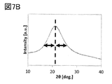
- FIG. 7B is a diagram illustrating the XRD spectrum of quartz glass
- 7C is a diagram illustrating the XRD spectrum of crystalline IGZO.
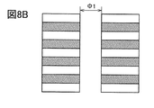
- 8A and 8B are cross-sectional views illustrating an example of a manufacturing process of a semiconductor device.
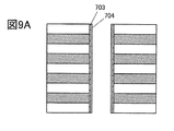
- 9A, 9B, and 9C are cross-sectional views illustrating an example of a manufacturing process of a semiconductor device.
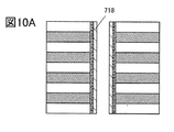
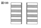
- 10A and 10B are cross-sectional views illustrating an example of a manufacturing process of a semiconductor device.
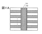
- 11A and 11B are cross-sectional views illustrating an example of a manufacturing process of a semiconductor device.
- 12A to 12C are diagrams illustrating an example of a manufacturing process of a semiconductor device.
- 13A is a top view illustrating an example of a manufacturing process of a semiconductor device, and FIGS.
- FIGS. 13B and 13C are cross-sectional views illustrating an example of a manufacturing process of a semiconductor device.
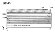
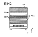
- 14A is a top view illustrating an example of a manufacturing process of a semiconductor device
- FIGS. 14B and 14C are cross-sectional views illustrating an example of a manufacturing process of a semiconductor device.
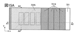
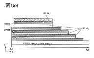
- 15A is a top view illustrating an example of a manufacturing process of a semiconductor device
- FIGS. 15B and 15C are cross-sectional views illustrating an example of a manufacturing process of a semiconductor device.
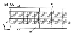
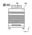
- 16A is a top view illustrating an example of a manufacturing process of a semiconductor device
- FIGS. 16B and 16C are cross-sectional views illustrating an example of a manufacturing process of a semiconductor device.
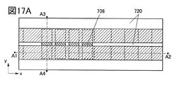
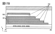
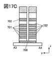
- FIGS. 17A is a top view illustrating an example of a manufacturing process of a semiconductor device
- FIGS. 17B and 17C are cross-sectional views illustrating an example of a manufacturing process of a semiconductor device.
- 18A is a top view illustrating an example of a manufacturing process of a semiconductor device
- FIGS. 18B and 18C are cross-sectional views illustrating an example of a manufacturing process of a semiconductor device.
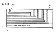
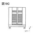
- 19A is a top view illustrating an example of a manufacturing process of a semiconductor device
- FIGS. 19B and 19C are cross-sectional views illustrating an example of a manufacturing process of a semiconductor device.
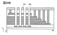
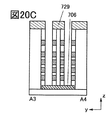
- 20A is a top view illustrating an example of a manufacturing process of a semiconductor device, and FIGS.
- 20B and 20C are cross-sectional views illustrating an example of a manufacturing process of a semiconductor device.
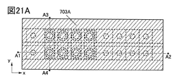
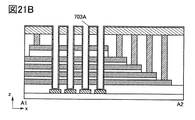
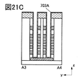
- 21A is a top view illustrating an example of a manufacturing process of a semiconductor device
- FIGS. 21B and 21C are cross-sectional views illustrating an example of a manufacturing process of a semiconductor device.
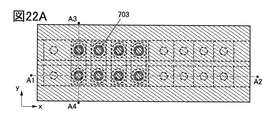
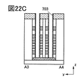
- 22A is a top view illustrating an example of a manufacturing process of a semiconductor device
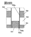
- FIGS. 22B, 22C, and 22D are cross-sectional views illustrating an example of a manufacturing process of a semiconductor device.
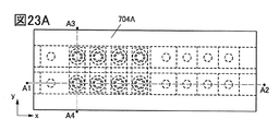
- 23A is a top view illustrating an example of a manufacturing process of a semiconductor device
- FIGS. 23B and 23C are cross-sectional views illustrating an example of a manufacturing process of a semiconductor device.
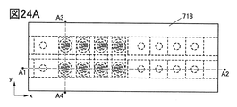
- FIGS. 24A is a top view illustrating an example of a manufacturing process of a semiconductor device
- FIGS. 24B and 24C are cross-sectional views illustrating an example of a manufacturing process of a semiconductor device.
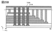
- 25A is a top view illustrating an example of a manufacturing process of a semiconductor device
- FIGS. 25B and 25C are cross-sectional views illustrating an example of a manufacturing process of a semiconductor device.
- 26A is a top view illustrating an example of a manufacturing process of a semiconductor device
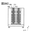
- FIGS. 26B and 26C are cross-sectional views illustrating an example of a manufacturing process of a semiconductor device.
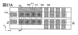
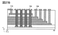
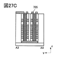
- 27A is a top view illustrating an example of a manufacturing process of a semiconductor device, and FIGS.
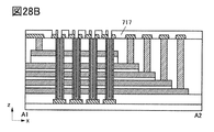
- FIGS. 28B and 28C are cross-sectional views illustrating an example of a manufacturing process of a semiconductor device.
- 28A is a top view illustrating an example of a manufacturing process of a semiconductor device
- FIGS. 28B and 28C are cross-sectional views illustrating an example of a manufacturing process of a semiconductor device.
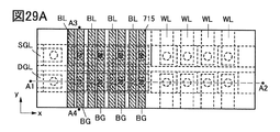
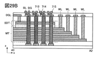
- 29A is a top view illustrating an example of a manufacturing process of a semiconductor device
- FIGS. 29B and 29C are cross-sectional views illustrating an example of a manufacturing process of a semiconductor device.
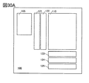
- 30A is a functional block diagram showing a configuration example of a memory device
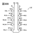
- FIG. 30B is a circuit diagram showing a configuration example of a memory string.
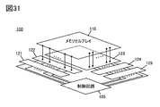
- FIG. 31 is a functional block diagram showing a configuration example of a storage device.
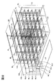
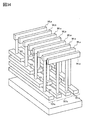
- FIG. 32 is a diagram showing a three-dimensional structural configuration example of a memory cell array.
- FIG. 33 is a diagram showing a three-dimensional structural configuration example of a memory cell array.
- FIG. 34 is a diagram showing a three-dimensional structural configuration example of a memory cell array.
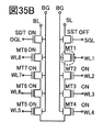
- 35A, 35B, and 35C are circuit diagrams for describing an operation example of the memory device.
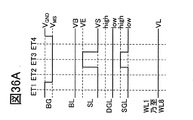
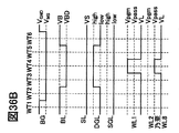
- 36A, 36B, and 36C are timing charts for explaining an operation example of the storage device.
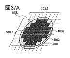
- 37A is a perspective view showing an example of a semiconductor wafer
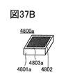
- FIG. 37B is a perspective view showing an example of a chip
- FIGS. 37C and 37D are perspective views showing examples of electronic components.
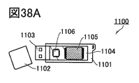
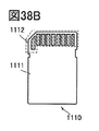
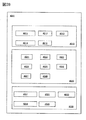
- 38A, 38B, 38C, 38D, and 38E are schematic diagrams of examples of the storage device.
- FIG. 39 is a block diagram showing a configuration example of an AI system.
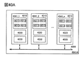
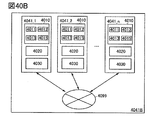
- 40A and 40B are block diagrams illustrating application examples of the AI system.
- 41A is a diagram showing an example of an electronic device
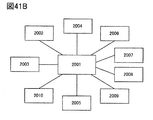
- FIG. 41B is a block diagram showing a configuration example of the electronic device.
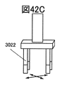
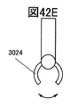
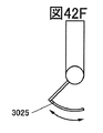
- 42A, 42B, 42C, 42D, 42E, and 42F are perspective views showing examples of electronic devices.
- the size, the layer thickness, or the region may be exaggerated for clarity. Therefore, it is not necessarily limited to that scale. It should be noted that the drawings schematically show ideal examples and are not limited to the shapes or values shown in the drawings. Further, in the drawings, the same reference numerals are commonly used in different drawings for the same portions or portions having similar functions, and repeated description thereof will be omitted. Further, when referring to the same function, the hatch patterns may be the same and may not be given a reference numeral in particular.
- the ordinal numbers given as the first, second, etc. are used for convenience, and do not indicate the order of steps or the order of stacking. Therefore, for example, the description can be made by appropriately replacing “first” with “second” or “third”.
- the ordinal numbers described in this specification and the like may be different from the ordinal numbers used to specify one embodiment of the present invention.
- the term “electrically connected” includes the case of being connected via “an object having some electrical action”.
- the “object having some kind of electrical action” is not particularly limited as long as it can transfer an electric signal between the connection targets.
- “things having some kind of electrical action” include electrodes and wirings, switching elements such as transistors, resistance elements, inductors, capacitors, and other elements having various functions.
- a nitride oxide refers to a compound in which the content of nitrogen is higher than that of oxygen.
- the oxynitride refers to a compound having a higher oxygen content than nitrogen.
- the content of each element can be measured using, for example, Rutherford backscattering spectroscopy (RBS).
- film and “layer” can be interchanged with each other.
- conductive layer to the term “conductive film”.
- insulating film to the term “insulating layer”.
- parallel means a state in which two straight lines are arranged at an angle of ⁇ 10° or more and 10° or less. Therefore, the case of -5° or more and 5° or less is also included.
- substantially parallel means a state in which two straight lines are arranged at an angle of ⁇ 30° or more and 30° or less.
- vertical means a state in which two straight lines are arranged at an angle of 80° or more and 100° or less. Therefore, the case of 85° or more and 95° or less is also included.
- substantially vertical means a state in which two straight lines are arranged at an angle of 60° or more and 120° or less.
- a crystal when a crystal is a trigonal crystal or a rhombohedral crystal, it is represented as a hexagonal system.
- a barrier film refers to a film having a function of suppressing permeation of impurities such as hydrogen and oxygen, and when the barrier film has conductivity, it is referred to as a conductive barrier film. There is.
- a metal oxide is a metal oxide in a broad sense. Metal oxides are classified into oxide insulators, oxide conductors (including transparent oxide conductors), oxide semiconductors (Oxide Semiconductor or simply OS), and the like. For example, when a metal oxide is used for the active layer of a transistor, the metal oxide may be referred to as an oxide semiconductor.
- FIG. 1 is a cross-sectional view of the memory cell array 700.
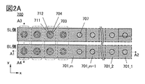
- FIG. 2A is a top view of the memory cell array 700. It should be noted that FIG. 2A is a top view of the plane indicated by the alternate long and short dash line of A5-A6 in FIG. 1, and some components are omitted. Further, FIG. 1 is a cross-sectional view of a portion indicated by a dashed-dotted line of A1-A2 in FIG. 2A. Further, FIG.
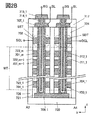
- FIG. 2B is a cross-sectional view of a portion indicated by an alternate long and short dash line of A3-A4 in FIG. 2A and is a cross-sectional view illustrating an example of the memory string.
- FIG. 3A is an enlarged cross-sectional view of the portion surrounded by the alternate long and short dash line 791 in FIG. 1, and is a diagram illustrating an example of the memory transistor MT functioning as a memory cell.
- FIG. 3B is an enlarged cross-sectional view of the portion surrounded by the alternate long and short dash line 792 in FIG. 1, and is a diagram illustrating an example of a transistor that functions as a selection transistor.
- FIG. 3A is an enlarged cross-sectional view of the portion surrounded by the alternate long and short dash line 791 in FIG. 1, and is a diagram illustrating an example of the memory transistor MT functioning as a memory cell.
- FIG. 3B is an enlarged cross-sectional view of the portion surrounded by the alternate long and short dash line
- a Cartesian coordinate system composed of x-axis, y-axis, and z-axis will be set and described for convenience.
- the x-axis and the y-axis are parallel to the upper surface of the base 720 on which the memory cell array 700 is provided, and the z-axis is vertical to the upper surface of the base 720.
- the memory cell array 700 includes an insulator 721 over a base 720, and a conductor 701 (conductors 701_1 to 701_m:m is a natural number of 2 or more) and an insulator 722 (insulator) on the insulator 721. 722_1 to insulator 722_m) are alternately laminated, a conductor 702 is provided on the laminate, and an insulator 724 is provided on the conductor 702 and the insulator 724.
- An insulator 703 (insulators 703_1 to 703_4) inside the opening formed so as to penetrate the conductor 702, the stacked body, and the insulator 721; and the inside of the insulator 703 is oxidized.
- Object 704 (oxide 704_1 to oxide 704_4), insulator 711 (insulator 711_1 to insulator 711_4) inside the oxide 704, and conductor 712 (conductor 712_1) inside the insulator 711.
- conductors 712_4 and the conductors 705 (conductors 705_1 through 705_4) electrically connected to the upper ends of the oxides 704_1 through 704_4, respectively.
- Conductors 706 (conductors 706_1 to 706_4) that are electrically connected to the lower ends, respectively, and conductors 707 (conductors 707_1 to 707_m) that are electrically connected to the conductors 701_1 to 701_m, respectively.
- a conductor 708 electrically connected to the conductors 707_1 to 707_m (conductors 708_1 to 708_m) and a conductor 709 electrically connected to the conductors 702.
- a conductor 710 electrically connected to the conductor 709, and an insulator 717 and an insulator 713 over the insulator 724, the conductor 705, the conductor 708, and the conductor 710.
- a conductor 714 (illustrated as a conductor 714_1 in FIG. 2B) and a conductor 715 (illustrated as a conductor 715_1 in FIG. 2B) are electrically connected to the conductors 712_1 to 712_4, respectively.
- the conductors 701 are displayed in four or more steps in order to represent the plurality of conductors 701; however, this embodiment is not limited to FIG. It is sufficient that the conductor 701 has two or more stages.
- the conductor 701 is provided so as to extend in the x-axis direction.
- the insulator 703 and the oxide 704 are provided so as to extend in the z-axis direction. That is, the conductor 701, the insulator 703, and the oxide 704 are preferably provided so as to cross each other at right angles.
- the conductor 707 is provided so as to extend in the z-axis direction.
- the conductor 708 may be provided so as to extend in the y-axis direction.
- a conductor functioning as the wiring BL connected to the conductor 705 may be provided by extending in the y-axis direction. Note that part of the conductor 705 may function as the wiring BL and the conductor may be provided so as to extend in the y-axis direction.
- the conductor 712 is formed in a columnar shape, and extends in the z-axis direction. Further, an insulator 711 is provided so as to surround the conductor 712, and an oxide 704 is provided so as to surround the insulator 711, each of which extends in the z-axis direction.
- the conductor 712 is provided like a core inside the columnar oxide 704 extending in the z-axis direction, and the insulator 711 is provided between the oxide 704 and the conductor 712.
- the insulator 703 is provided so as to surround the periphery of the columnar oxide 704.
- the conductor 707 is formed in a columnar shape and is provided so as to extend in the z-axis direction.
- the columnar oxide 704 is electrically connected to the conductor 706 at the lower end in the z-axis direction and is electrically connected to the conductor 705 at the upper end. Further, as shown in FIG. 2B, the conductor 706 is electrically connected to the lower ends of two adjacent columnar oxides 704, and the upper ends of the two columnar oxides 704 are electrically separated from each other. It is electrically connected to the conductor 705.
- a U-shaped memory string in which two columnar oxides 704 are electrically connected by a conductor 706 is described; however, the present invention is not limited to this.
- the conductor 706 may be one of the bit line BL and the source line SL, and the conductor 705 may be the other of the bit line BL and the source line SL.
- the conductor 706 may be electrically connected to the plurality of columnar oxides 704 or may be electrically connected to one columnar oxide 704.
- the conductor 705 may be electrically connected to the plurality of columnar oxides 704 or may be electrically connected to one columnar oxide 704.
- the select transistor is provided near the lower end of the columnar oxide 704 and near the upper end. Is preferably provided.
- the selection transistor SST and the conductor 705 and the memory transistor MT are provided between the conductor 706 and the memory transistor MT.
- a select transistor SDT is provided in between.
- a region where the conductor 701 intersects with the insulator 703 and the oxide 704 and the vicinity thereof function as the memory transistor MT.
- a region where the conductor 702 intersects with the insulator 703 and the oxide 704 and the vicinity thereof function as a selection transistor.
- the channel length directions of these memory transistor MT and select transistor are parallel to the z axis.
- the memory transistor MT and the selection transistor are electrically connected in series to form a memory string.
- FIG. 3A is an enlarged cross-sectional view of the portion surrounded by the alternate long and short dash line 791 in FIG. FIG.
- the memory transistor MT includes the conductor 701_k, the insulator 703 (the insulator 703a, the insulator 703b, and the insulator 703c), and the oxide 704 (the oxide 704a, the oxide 704b, and the oxide 704c). ..
- the memory transistor MT may include the conductor 712 and the insulator 711.
- the conductor 701_k functions as a gate of the memory transistor MT
- the insulator 703a functions as a gate insulating layer
- the insulator 703b functions as a charge storage layer
- the insulator 703c functions as a tunnel insulating layer.
- the oxide 704 includes an oxide 704a, an oxide 704b, and an oxide 704c.
- the oxide 704a has a relatively wide energy gap with respect to the oxide 704b, and thus the oxide 704a has a large energy gap.
- the object 704c has a relatively wide energy gap with respect to the oxide 704b. In other words, the oxide 704b has a relatively narrow energy gap with respect to the oxide 704a and the oxide 704c.
- the oxide 704 included in the k-th memory transistor MT functions as a channel formation region. Further, the oxide 704 between the kth stage memory transistor MT and the k ⁇ 1th stage memory transistor MT, and the oxide 704 between the kth stage memory transistor MT and the k+1th stage memory transistor MT are It is preferable to function as a low resistance region.
- the oxide 704 has a structure in which a channel formation region and a low resistance region are alternately formed, so that series resistance between memory cells can be reduced in a memory string in which memory cells are stacked or a memory cell array. it can.
- the conductor 701_k functions as a first gate and the conductor 712 functions as a second gate.
- the first gate may be simply referred to as a gate or a control gate
- the second gate may be referred to as a back gate.
- An insulator 711 is provided between the oxide 704 and the conductor 712 and functions as a second gate insulating layer.
- the insulator 703a functions as a first gate insulating layer.
- the power consumption of the memory transistor MT can be reduced by controlling the potential of the conductor 712 which functions as the second gate.
- FIG. 3B is an enlarged cross-sectional view of the portion surrounded by the alternate long and short dash line 792 in FIG. 1, showing a cross section of the select transistor (bit line side transistor: SDT and source line side transistor: SST).
- the selection transistor includes the conductor 702, the insulator 703, and the oxide 704 (the oxide 704a, the oxide 704b, and the oxide 704c). Further, the conductor 712 and the insulator 711 may be included.
- the conductor 702 functions as a gate of the selection transistor, and the insulator 703a functions as a gate insulating layer.
- the gate insulating layer may include at least the insulator 703a, and the insulator 703b and the insulator 703c may not be provided. Alternatively, after the insulator 703a, the insulator 703b, and the insulator 703c are provided, the insulator 703b and the insulator 703c may be partially removed.
- the oxide 704 includes the oxide 704a, the oxide 704b, and the oxide 704c.
- the oxide 704a has a relatively wide energy gap with respect to the oxide 704b
- the oxide 704c has the oxide 704b.
- the energy gap is relatively wide.
- the oxide 704b has a relatively narrow energy gap with respect to the oxide 704a and the oxide 704c.
- the conductor 702 functions as a first gate and the conductor 712 functions as a second gate.
- the first gate may be simply called a gate or a top gate, and the second gate may be called a back gate.
- An insulator 711 is provided between the oxide 704 and the conductor 712 and functions as a second gate insulating layer. At this time, the insulator 703a functions as a first gate insulating layer.
- the threshold value of the selection transistor can be controlled by the conductor 712 which functions as the second gate.
- the structure of the semiconductor device described in this embodiment is an example, and the present invention is not limited to the number and arrangement of circuit elements, wirings, and the like shown in the drawings and the like according to this embodiment. ..
- the number, arrangement, and the like of circuit elements and wirings included in the semiconductor device according to this embodiment can be set as appropriate in accordance with the circuit configuration and the driving method.
- the base 720 on which the memory cell array 700 is provided preferably has an insulating surface.
- a semiconductor substrate having an insulator formed on its surface an insulator substrate, a conductor substrate having an insulator formed on its surface, or the like may be used.
- the semiconductor substrate for example, a semiconductor substrate made of any one of silicon and germanium, or any one of silicon carbide, silicon germanium, gallium arsenide, indium phosphide, zinc oxide, gallium oxide, etc.
- a semiconductor substrate or the like may be used.
- a glass substrate for example, a glass substrate, a quartz substrate, a sapphire substrate, a stabilized zirconia substrate (yttria-stabilized zirconia substrate, etc.), a resin substrate, or the like may be used.
- a substrate having an insulator region in the semiconductor substrate described above for example, an SOI (Silicon On Insulator) substrate or the like may be used.
- a graphite substrate, a metal substrate, an alloy substrate, a conductive resin substrate, or the like may be used as the conductor substrate.
- the conductor 701 functions as the gate of the memory transistor MT and is electrically connected to the word line. That is, the conductor 701, the conductor 707, and the conductor 708 also function as part of the word line.
- the conductor 701 is provided in a step shape in which the conductor 701 in the lower layer extends toward the A2 side from the conductor 701 in the upper layer.
- a conductive material such as silicon to which impurities are added or metal can be used.
- silicon is used as the conductor 701
- amorphous silicon, microcrystalline silicon, polycrystalline silicon, single crystal silicon, or the like can be used.
- p-type impurities or n-type impurities may be added in order to give silicon conductivity.
- the conductive material containing silicon silicide containing titanium, cobalt, or nickel can be used as the conductor 701.
- a metal material aluminum, chromium, copper, silver, gold, platinum, tantalum, nickel, titanium, molybdenum, tungsten, hafnium, vanadium, niobium, manganese, magnesium, zirconium, beryllium, indium,
- a material containing one or more metal elements selected from ruthenium and the like can be used.
- the conductor 702 is provided on the conductor 701.
- the conductor 702 functions as a gate of a selection transistor (a selection transistor on the bit line side: SDT and a selection transistor on the source line side: SST) and is electrically connected to the wiring DGL or the wiring SGL. That is, the conductor 702, the conductor 709, and the conductor 710 also function as part of the wiring DGL or the wiring SGL.
- the conductor 702 can be formed using the same material as the conductor 701.
- the conductor 702 may be made of the same material as the conductor 701 or may be made of a different material.
- the conductor 701 and the conductor 702 may be determined in consideration of a work function or the like depending on applications.
- an insulating oxide, a nitride, an oxynitride, a nitride oxide, a metal oxide, a metal oxynitride, or a metal nitriding oxide is used as an insulating film provided in the upper and lower layers of the conductor 701 and the conductor 702.
- a thing etc. can be used.
- silicon oxide, silicon oxynitride, silicon nitride oxide, silicon nitride, fluorine-added silicon oxide, carbon-added silicon oxide, carbon-nitrogen-added silicon oxide, silicon oxide having pores, or resin is Since it has a low dielectric constant, it is suitable for use in the insulating film.
- the insulating film aluminum oxide, gallium oxide, hafnium oxide, zirconium oxide, an oxide containing aluminum and hafnium, an oxynitride containing aluminum and hafnium, an oxide containing silicon and hafnium, and an oxide containing silicon and hafnium It is possible to use a nitride or a nitride containing silicon and hafnium, but since these have a high relative dielectric constant, parasitic capacitance may occur between the conductors 701 or between the conductors 701 and 702. .
- the material used for the insulating film can be determined according to the device design and application.
- the insulator 703 has an insulator 703a, an insulator 703b, and an insulator 703c.
- the insulator 703a is provided on the conductor 701 side
- the insulator 703c is provided on the oxide 704 side
- the insulator 703b is provided between the insulator 703a and the insulator 703c.
- the insulator 703a functions as a gate insulating layer
- the insulator 703b functions as a charge storage layer
- the insulator 703c functions as a tunnel insulating layer.
- the selection transistor may have the same structure as the memory transistor MT.
- the charge storage layer and the tunnel insulating layer may not be provided in the selection transistor.
- the insulator 703b and the insulator 703c may be removed and only the insulator 703a may be provided as the insulator 703.
- the insulator 703b and the insulator 703c may not be provided and only the insulator 703a may be provided as the insulator 703.
- a conductor 712 may be provided as the second gate electrode.
- the conductor 702 functions as a first gate electrode
- the insulator 703a functions as a first gate insulating film
- the insulator 711 functions as a second gate insulating film.
- the conductor 712 can control the threshold value of the selection transistor.
- silicon oxide, silicon oxynitride, or the like it is preferable to use silicon oxide, silicon oxynitride, or the like as the insulator 703a.
- silicon oxide, silicon oxynitride, or the like aluminum oxide, hafnium oxide, zirconium oxide, or an oxide containing two or more selected from aluminum, hafnium, and zirconium may be used. Alternatively, these may be stacked to form the insulator 703a.
- the insulator 703b is preferably made of a material that functions as a charge storage layer, and is preferably made of silicon nitride or silicon nitride oxide. Further, it may have aluminum oxide, hafnium oxide, zirconium oxide, or an oxide containing two or more selected from aluminum, hafnium, and zirconium.
- silicon oxide or silicon oxynitride it is preferable to use silicon oxide or silicon oxynitride as the insulator 703c.
- silicon oxide or silicon oxynitride aluminum oxide, hafnium oxide, zirconium oxide, or an oxide containing two or more selected from aluminum, hafnium, and zirconium may be used. Alternatively, these may be stacked to form the insulator 703c.
- At least one of the insulator 703a, the insulator 703b, and the insulator 703c includes, for example, aluminum oxide, hafnium oxide, tantalum oxide, zirconium oxide, lead zirconate titanate (PZT), strontium titanate (SrTiO 3 ) or An insulator including a so-called high-k material such as (Ba,Sr)TiO 3 (BST) may be used in a single layer or a laminated layer.
- any one of the insulator 703a, the insulator 703b, and the insulator 703c has a stacked structure
- a three-layer stack in which zirconium oxide, aluminum oxide, and zirconium oxide are sequentially formed, or zirconium oxide A four-layer stack in which aluminum oxide, zirconium oxide, and aluminum oxide are sequentially formed may be used.
- a compound containing hafnium and zirconium may be used for at least one of the insulators 703a, 703b, and 703c.
- the insulator 703c functions as a tunnel insulating layer, so that the oxide 704 and the insulator 702b pass through the insulator 703c in the data writing operation or the data erasing operation to the memory transistor MT. In between, charge transfer occurs.
- the insulator 703c in order for the insulator 703c to function as a tunnel insulating layer, the insulator 703c preferably has a smaller thickness than the insulator 703a.
- the insulator 703 formed at the bottom of the opening is formed by dry etching or the like. It must be removed by isotropic etching. During the anisotropic etching, the insulator 703c is also exposed to plasma, radicals, gas, chemical solution, etc., even on the side surface. When the side surface of the insulator 703c is damaged by these, a trap center is generated in the insulator 703c, which might affect the electrical characteristics of the transistor.
- the side surface of the insulator 703c is required to have high resistance to damage due to etching.
- the insulator 703a, the insulator 703b, and the insulator 703c can be formed by an ALD method or a CVD method.
- ALD method atomic layer deposition method
- CVD method vapor deposition method
- exposure to an air atmosphere is performed in the same chamber or by using a multi-chamber deposition apparatus having a plurality of chambers. Instead, it is preferable to form the film continuously.
- oxide 704 it is preferable to use a metal oxide which functions as an oxide semiconductor (hereinafter also referred to as an oxide semiconductor).
- an In-M-Zn oxide (the element M is aluminum, gallium, yttrium, copper, vanadium, beryllium, boron, titanium, iron, nickel, germanium, zirconium, molybdenum, lanthanum, cerium, neodymium).
- the oxide 704 an In—Ga oxide, an In—Zn oxide, an In oxide, or the like may be used.
- the oxide 704 preferably includes an oxide 704a provided on the insulator 703c side, an oxide 704b provided inside the oxide 704a, and an oxide 704c provided inside the oxide 704b.
- the oxide 704a is preferably an oxide having a relatively wide energy gap with respect to the oxide 704b.
- the oxide 704c is preferably an oxide having a relatively wide energy gap with respect to the oxide 704b.
- an oxide having a wide energy gap may be referred to as an oxide having a wide gap and an oxide having a narrow energy gap may be referred to as an oxide having a narrow gap.
- the oxide 704 has a three-layer structure of the oxide 704a, the oxide 704b, and the oxide 704c in FIGS. 3A and 3B, the invention is not limited to this.
- the oxide 704 may have a two-layer structure of the oxide 704a and the oxide 704b, or may have a stacked structure of four or more layers.
- the energy of the bottom of the conduction band of the oxide 704a and the oxide 704c is higher than the energy of the bottom of the conduction band of the oxide 704b. It is preferable that In other words, it is preferable that the electron affinity of the oxide 704a and the oxide 704c be smaller than the electron affinity of the oxide 704b.
- the oxide 704a, the oxide 704b, and the oxide 704c are preferably combined in a different atomic ratio of each metal atom.
- the atomic number ratio of the element M in the constituent elements is the atom of the element M in the constituent element in the metal oxide used for the oxide 704b. It is preferably larger than the number ratio.
- the atomic ratio of the element M to In is preferably higher than the atomic ratio of the element M to In in the metal oxide used for the oxide 704b. ..
- the atomic ratio of In to the element M is preferably higher than the atomic ratio of In to the element M in the metal oxide used for the oxides 704a and 704c. ..
- a metal oxide having a composition of 1, a composition in the vicinity of any one of these, or the like can be used.
- a metal oxide having a composition of 3 to 4.1 and a composition in the vicinity thereof is preferable.
- the above composition indicates the atomic ratio in the oxide formed on the substrate or the atomic ratio in the sputtering target.
- increasing the In ratio as the composition of the oxide 704b is preferable because the on-state current, field-effect mobility, or the like of the transistor can be increased.
- increasing the In ratio of the oxide 704b often results in normally-on transistor characteristics.
- a method for operating a semiconductor device which has favorable normally-on transistor characteristics can be provided. Note that details of a method for operating the semiconductor device of one embodiment of the present invention will be described later.
- normally-on refers to a state in which a channel exists and a current flows through a transistor even when a voltage is not applied to the gate.
- normally-off means that when a potential is not applied to the gate or a ground potential is applied to the gate, the current per channel width of 1 ⁇ m flowing in the transistor is 1 ⁇ 10 ⁇ 20 A or less at room temperature and 85° C. It means 1 ⁇ 10 ⁇ 18 A or less, or 1 ⁇ 10 ⁇ 16 A or less at 125° C.
- CAAC-OS described later be used as the oxide 704a and the oxide 704c and CAC-OS be used as the oxide 704b.
- the c-axis is parallel to the xy plane illustrated in FIGS. 1 and 2, that is, perpendicular to the z-axis and is centered from the side surface of the opening. It is preferably oriented so as to face.
- the bottom of the conduction band changes gently at the junction between the oxide 704a and the oxide 704b and at the junction between the oxide 704c and the oxide 704b.
- the conduction band bottoms at the junction between the oxide 704a and the oxide 704b and the junction between the oxide 704c and the oxide 704b continuously change or continuously join.
- the density of defect states in the mixed layer formed at the interface between the oxide 704a and the oxide 704b and the interface between the oxide 704c and the oxide 704b be low.
- the oxide 704a, the oxide 704b, and the oxide 704c have a common element other than oxygen (as a main component), so that a mixed layer with low defect level density can be formed. it can.
- the oxide 704b is an In—Ga—Zn oxide
- In—Ga—Zn oxide, Ga—Zn oxide, gallium oxide, or the like may be used as the oxide 704a and the oxide 704c.
- the density of defect states in the interface between the oxide 704a and the oxide 704b and the interface between the oxide 704c and the oxide 704b can be reduced. Therefore, the influence of interface scattering on carrier conduction is reduced, and the memory transistor MT can obtain a high on-current.
- oxide 704 Note that a more detailed description of the metal oxide that can be used as the oxide 704 will be described later.
- FIG. 3A is an enlarged view of the memory transistor MT surrounded by the alternate long and short dash line 791 in FIG. As illustrated in FIG. 3A, the oxide 704b is provided so as to be sandwiched between the oxide 704a and the oxide 704c.
- the carrier having a narrow gap is mainly Flowing Therefore, in the case of using the above structure, by sandwiching the oxide 704b having a narrow gap with the oxide 704a having a wide gap and the oxide 704c, carriers flowing in the oxide 704 can be confined in the oxide 704b, In the ON state of the transistor, a high current driving force, that is, a large ON current and a high field effect mobility can be obtained.
- the oxide 704a between the oxide 704b and the insulator 703c the oxide 704b serving as a carrier path is not directly in contact with the insulator 703c, so that formation of a trap center is suppressed.
- the transistor and a semiconductor device including the transistor can have high reliability.
- the metal film, the oxide film containing a metal element, or the nitride film containing a metal element has a property of absorbing hydrogen
- hydrogen in the oxide 704 is It is absorbed into the membrane. Therefore, hydrogen which is an impurity in the oxide 704 can be reduced.
- the metal film, the oxide film containing a metal element, or the nitride film containing a metal element may be removed together with hydrogen absorbed from the oxide 704 in a later step. As a result, the oxide 704 is highly purified (reduction of impurities such as water and hydrogen) and has higher resistance.
- the metal film, the oxide film containing a metal element, or the nitride film containing a metal element does not necessarily have to be removed.
- a metal film, an oxide film containing a metal element, or a nitride film containing a metal element is oxidized by oxygen absorbed from the oxide 704 and becomes an insulator and has high resistance, it may be left. .. In that case, as in the case of the insulator 711, it may function as the second gate insulating layer.
- heat treatment is performed to oxidize the conductive region.
- the metal film, the oxide film containing a metal element, or the nitride film containing a metal element serves as an insulator and has high resistance.
- the heat treatment is preferably performed in an oxidizing atmosphere, for example.
- heat treatment is performed to perform the metal film, the oxide film containing the metal element, or the metal element.
- the nitride film having OH reacts with oxygen contained in the structure and is oxidized.
- the oxide film containing a metal element, or the nitride film containing a metal element can function as a second gate insulating layer similarly to the insulator 711.
- a metal film, an oxide film containing a metal element, or a nitride film containing a metal element is preferably provided with a thickness of 0.5 nm to 5 nm, preferably 1 nm to 2 nm.
- aluminum having a thickness of 0.5 nm to 5 nm is oxidized by heat treatment, aluminum oxide having a thickness of 0.7 nm to 8 nm may be obtained.
- the oxide 704 is in contact with the metal film, the oxide film containing a metal element, or the nitride film containing a metal element in an atmosphere containing nitrogen. It is preferable to perform the heat treatment once. By performing heat treatment once in an atmosphere containing nitrogen, oxygen in the oxide 704 easily diffuses into a metal film, an oxide film containing a metal element, or a nitride film containing a metal element.
- a memory transistor or a selection transistor including an oxide semiconductor when impurities and oxygen vacancies are present in a region where a channel is formed in the oxide semiconductor, electric characteristics are likely to vary and reliability is deteriorated. There is.
- oxygen deficiency when oxygen deficiency is included in a region where a channel is formed in the oxide semiconductor, the transistor is likely to have normally-on characteristics. Therefore, it is preferable that oxygen vacancies in the region where the channel is formed be reduced as much as possible.
- the memory transistor may be operated with normally-on characteristics depending on the specifications of the semiconductor device.
- the same material as the conductor 701 can be used as the conductor 712. Since the conductor 712 needs to be formed inside the opening having a large aspect ratio (in other words, the oxide 704 and the concave portion of the insulator 711), it is formed by a CVD method, an ALD method, or a plating method. It is preferable. At this time, the insulator 711 can be formed using the same material as the insulator 703.
- the insulator 711 is preferably a material that can supply oxygen to the oxide 704.
- oxygen can be supplied to the oxide 704 in some cases.
- the oxide 704 is highly purified.
- the memory transistor MT and the semiconductor device including the memory transistor MT can have high reliability.
- the insulator 711 may be a material capable of supplying impurities such as hydrogen and nitrogen.
- the insulator 711 for example, by using an oxide containing hydrogen or nitrogen, hydrogen or nitrogen can be supplied to the oxide 704 in some cases.
- the resistance value of the oxide 704 may be reduced.
- the memory transistor MT can be operated with a lower driving voltage. Further, in the ON state of the memory transistor MT, a high current drivability, that is, a large ON current and a high field effect mobility can be obtained.
- the opening formed in the stacked body in which the memory transistor MT is provided has an upper surface having a circular shape in FIG. 2A and the like; however, the opening is not limited to this.
- the upper surface may have an elliptical shape, a triangular shape, or a quadrangular shape. It may be a polygonal shape such as. Further, in the case of a polygonal shape, the corners may be rounded.
- the top shapes of the insulator 703 and the oxide 704 may change in accordance with the top shape of the opening. Further, the opening may have a shape in which the cross-sectional area of the opening on the lower side (conductor 706 side) is narrower than that of the opening on the upper side (conductor 705 side).
- the oxide transistor 704, the insulator 703, and the conductor 701 form a memory transistor MT.
- 1 and 2 show an example in which the memory transistors MT are stacked in m stages (m is a natural number of 2 or more). Note that in FIGS. 1 and 2, the conductor 701 is displayed in four or more steps to represent the plurality of conductors 701; however, this embodiment is not limited to FIG. 1 and at least the conductor 701 is illustrated. It suffices to have two or more stages.
- the conductor 705 is electrically connected to the oxide 704 and functions as part of the source line SL or the bit line BL.
- a conductive material containing a metal element is preferably used.
- a material having conductivity can be used among the materials that can be used for the above metal film, the oxide film containing a metal element, or the nitride film containing a metal element. In this case, part of the oxide 704 has low resistance.
- a metal compound layer containing a metal element of the conductor 705 and a component of the oxide 704 is preferably formed at the interface between the conductor 705 and the oxide 704.
- the formation of the metal compound layer is preferable because the contact resistance between the conductor 705 and the oxide 704 is reduced.
- the conductor 705 absorbs oxygen contained in the oxide 704, and the resistance of the oxide 704 near the interface between the conductor 705 and the oxide 704 is reduced, whereby the conductor 705 and the oxide 704 are The contact resistance of can be reduced.
- the conductor 706 is electrically connected to the oxide 704 electrically connected to the conductor 706 functioning as part of the bit line BL and the conductor 705 functioning as part of the source line SL.
- a memory string is formed by electrically connecting the oxide 704 and the oxide 704.
- the area surrounded by the dotted line in FIG. 2A represents a memory string. That is, FIG. 2A shows a memory cell array 700 having four memory strings.
- the same material as the conductor 705 can be used for the conductor 706.
- a material having conductivity can be used among the materials that can be used for the above metal film, the oxide film containing a metal element, or the nitride film containing a metal element. In this case, as described above, part of the oxide 704 has low resistance.
- the conductor 706 may be made of the same material as the conductor 705 or may be made of a different material.
- a metal compound layer containing a metal element of the conductor 706 and a component of the oxide 704 is formed at the interface between the conductor 706 and the oxide 704.
- the formation of the metal compound layer is preferable because the contact resistance between the conductor 706 and the oxide 704 is reduced.
- the conductor 706 absorbs oxygen contained in the oxide 704, and the resistance of the oxide 704 near the interface between the conductor 706 and the oxide 704 is reduced, whereby the conductor 706 and the oxide 704 are The contact resistance of can be reduced.
- a material which can be used for the conductor 701, the conductor 702, or the conductor 712 is used in the same manner. You can The respective conductors may use the same material or different materials.
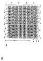
- FIG. 4 is a top view illustrating a memory cell array 700A in which a plurality of memory cell arrays 700 having six stages of memory transistors MT are combined.
- some components are omitted for ease of explanation.
- the selection transistors bit line side transistor SDT and source line side transistor SST
- the conductor 701 and the conductor 702 that is a component thereof are omitted.
- the conductor 715 that functions as a part of the wiring BG that is electrically connected to the conductor 712 that functions as the second gate is shown by a solid line.
- each memory cell array 700 has four memory strings each having six stages of memory transistors MT.
- the end on the bit line side of the memory string is electrically connected to different bit lines BL (bit lines BL_1 to BL_4).
- bit lines BL_1 to BL_4 bit lines BL_1 to BL_4.
- the end of the memory string on the source line side is electrically connected to the source line SL and is supplied with a common potential.
- the source line SL may be grounded or may be given a constant potential. Further, the potential may be changed according to the operation of the circuit.
- the conductors 701_1 to 701_6 are electrically connected to different word lines WL.
- the conductors 701_1 to 701_6 on the bit line side are electrically connected to the word lines WLa_1 to WLa_6, respectively, and the conductors 701_1 to 701_6 on the source line side are connected to the word lines WLb_1 to WLb_6, respectively. It is electrically connected.
- the conductor 712 included in each memory string is electrically connected to the wiring BG.
- FIG. 4 illustrates an example in which the conductors 712 arranged in the column direction are electrically connected to the common wiring BG, the present invention is not limited to this.
- the conductors 712 arranged in the row direction may be electrically connected to the common wiring BG.
- a different potential may be applied to each wiring BG, or the same potential may be applied to a plurality of wirings BG.
- the plurality of wirings BG are electrically connected to each other.
- the plurality of wirings BG may refer to all the wirings BG included in the memory cell array 700A.
- the wiring BG may be referred to as a circuit which controls the potential of the wiring BG (eg, a BG driver or a BG driver circuit. Further, a driver or a driver). It may be referred to as a circuit)).
- the BG driver circuit may be provided for each wiring BG, or a plurality of wirings BG may be electrically connected to one BG driver circuit.
- the memory cell array 700A may include one BG driver circuit, and all the wirings BG included in the memory cell array 700A may be electrically connected to the BG driver circuit.
- bit line BL bit line BL_1 to bit line BL_4
- word line WLa_1 to word line WLa_6 and word line WLb_1 to word line WLb_6 an arbitrary memory transistor in the memory cell array 700 is selected.
- MT can be selected.
- writing, reading, erasing, and the like can be performed on the selected memory transistor MT.
- a selection transistor (not shown) is provided in each memory string, an arbitrary memory cell array 700 in the memory cell array 700A is selected, and an arbitrary memory transistor MT in the selected memory cell array 700 is selected. Then, writing, reading and erasing can be performed.
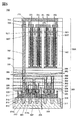
- FIG. 5 illustrates a configuration example of a memory device 750 in which the memory cell array 700A is stacked and provided over the circuit 300. As illustrated in FIG. 5, the memory cell array 700A is stacked and provided in a region where the circuit 300 including the transistor 301, the transistor 302, and the transistor 303 is formed. Note that the transistor 301 and the transistor 302 form a sense amplifier 304, and the transistor 303 functions as a column selection switch.
- bit line BL of the memory cell array 700A is electrically connected to one of a source and a drain of the transistor 301, and a gate of the transistor 301 is electrically connected to one of a source and a drain of the transistor 302, The gate of the transistor 302 is electrically connected to the other of the source and the drain of the transistor 301. Further, one of a source and a drain of the transistor 301 and the other of the source and the drain of the transistor 302 are electrically connected to one of a source and a drain of the transistor 303 which functions as a column selection switch. Accordingly, the layout area of the storage device 750 can be reduced. Note that FIG.
- FIG. 5 shows an example in which 10 stages of memory transistors MT are provided and 20 memory transistors MT are provided for each memory string.
- the number of stacked memory transistors MT is not limited to this. For example, 32 layers, 64 layers, 128 layers may be laminated, or 200 layers or more may be laminated.
- the bit line BL of the memory cell array 700A is electrically connected to the sense amplifier 304 and the transistor 303 functioning as a column selection switch through a conductor 752 formed so as to be embedded in an insulator 726, an insulator 722, or the like. Connected.
- the circuits and transistors included in the circuit 300 are examples, and one embodiment of the present invention is not limited to the circuit structure or the transistor structure.
- appropriate circuits and transistors such as a control circuit, a row decoder, a row driver, a source line driver, and an input/output circuit can be provided depending on the structure of the memory device 750 and its driving method.
- the transistor 301, the transistor 302, and the transistor 303 are provided over the substrate 311, and are a conductor 316, an insulator 315, a semiconductor region 313 which is part of the substrate 311, and a low-resistance region functioning as a source region or a drain region, respectively. 314a and a low resistance region 314b. Note that as illustrated in FIG. 5, one low-resistance region may be shared as one source region or drain region and the other source region or drain region of the transistors 301 and 302.
- a semiconductor region 313 (a part of the substrate 311) in which a channel is formed has a convex shape. Further, the side surface and the upper surface of the semiconductor region 313 are provided so as to cover the conductor 316 with the insulator 315 interposed therebetween. Note that the conductor 316 may be formed using a material whose work function is adjusted.
- Such a transistor 301, a transistor 302, and a transistor 303 use a convex portion of a semiconductor substrate, and thus are also called FIN transistors.
- an insulator which functions as a mask for forming the protrusion may be provided in contact with the top of the protrusion.
- the SOI substrate may be processed to form a semiconductor film having a convex shape.
- the transistor 301, the transistor 302, and the transistor 303 may each be a p-channel type or an n-channel type, but the transistor 301 and the transistor 302 are preferably transistors having different polarities.
- a region such as a region where a channel of the semiconductor region 313 is formed, a region in the vicinity thereof, a low resistance region 314a serving as a source region or a drain region, a low resistance region 314b, or the like preferably contains a semiconductor such as a silicon-based semiconductor. It preferably includes crystalline silicon. Alternatively, a material including Ge (germanium), SiGe (silicon germanium), GaAs (gallium arsenide), GaAlAs (gallium aluminum arsenide), or the like may be used. It is also possible to adopt a configuration using silicon in which the effective mass is controlled by applying stress to the crystal lattice and changing the lattice spacing. Alternatively, the transistors 301, 302, and 303 may be HEMTs (High Electron Mobility Transistors) by using GaAs and GaAlAs.
- HEMTs High Electron Mobility Transistors
- the low-resistance region 314a and the low-resistance region 314b impart an n-type conductivity imparting element such as arsenic or phosphorus or a p-type conductivity imparting boron, in addition to the semiconductor material applied to the semiconductor region 313. Including the element to do.
- the insulator 315 functions as a gate insulating film of the transistors 301, 302, and 303.
- the conductor 316 functioning as a gate electrode is a semiconductor material such as silicon, a metal material, or an alloy containing an element imparting n-type conductivity such as arsenic or phosphorus, or an element imparting p-type conductivity such as boron. Materials or conductive materials such as metal oxide materials can be used.
- the work function is determined by the material of the conductor, so the threshold voltage can be adjusted by changing the material of the conductor. Specifically, it is preferable to use a material such as titanium nitride or tantalum nitride for the conductor. Furthermore, in order to achieve both conductivity and embedding properties, it is preferable to use a metal material such as tungsten or aluminum as a laminate for the conductor, and it is particularly preferable to use tungsten in terms of heat resistance.
- an insulator 317 functioning as an etch stopper is provided above the conductor 316.
- an insulator 318 functioning as a spacer is preferably provided on a side surface of the insulator 315.
- the conductor 328 By forming the conductor 328 in the opening formed in this manner, a favorable contact with reduced contact resistance can be obtained between the low resistance region 314a and the low resistance region 314b and the conductor 328.
- the low resistance region 314a thus formed and the contact between the low resistance region 314b and the conductor 328 may be referred to as a self-aligned contact.
- An insulator 320, an insulator 322, an insulator 324, an insulator 326, and an insulator 327 are sequentially stacked to cover the transistor 301, the transistor 302, and the transistor 303.
- the insulator 320, the insulator 322, the insulator 324, the insulator 326, and the insulator 327 for example, silicon oxide, silicon oxynitride, silicon nitride oxide, silicon nitride, aluminum oxide, aluminum oxynitride, aluminum nitride oxide, or nitride is used. Aluminum or the like may be used.
- the insulator 322 may have a function as a flattening film for flattening a step caused by the transistor 301 and the like provided below the insulator 322.
- the upper surface of the insulator 322 may be planarized by a planarization treatment using a chemical mechanical polishing (CMP) method or the like in order to enhance planarity.
- CMP chemical mechanical polishing
- the insulator 324 it is preferable to use a film having a barrier property such that hydrogen and impurities do not diffuse from the substrate 311, the transistor 301, or the like to a region where the memory cell array 700A is provided.
- a film having a barrier property against hydrogen for example, silicon nitride formed by a CVD method can be used.
- silicon nitride formed by a CVD method when hydrogen is diffused into a semiconductor element including an oxide semiconductor, such as the memory transistor MT, characteristics of the semiconductor element may be deteriorated in some cases. Therefore, it is preferable to use a film which suppresses diffusion of hydrogen between the memory transistor MT and the transistor 301 and the like.
- the film that suppresses the diffusion of hydrogen is a film in which the amount of released hydrogen is small.
- the desorption amount of hydrogen can be analyzed by using, for example, a thermal desorption gas analysis method (TDS).
- TDS thermal desorption gas analysis method
- the desorption amount of hydrogen in the insulator 324 is calculated as the desorption amount converted into hydrogen atoms per area of the insulator 324 when the surface temperature of the film is in the range of 50 °C to 500 °C. Therefore, it may be 10 ⁇ 10 15 atoms/cm 2 or less, preferably 5 ⁇ 10 15 atoms/cm 2 or less.
- the insulators 326 and 327 preferably have a lower dielectric constant than the insulator 324.
- the relative permittivity of the insulator 326 and the insulator 327 is preferably less than 4, and more preferably less than 3.
- the relative permittivity of the insulator 326 and the insulator 327 is preferably 0.7 times or less, and more preferably 0.6 times or less that of the insulator 324.
- the insulator 317, the insulator 320, the insulator 322, the insulator 324, the insulator 326, and the insulator 327 include a conductor 328, a conductor 329, a conductor 330, and the like which are electrically connected to the memory cell array 700A. It is embedded. Note that the conductor 328, the conductor 329, and the conductor 330 have a function as a plug or a wiring. The conductor 329 is embedded in the openings of the insulator 317 and the insulator 322, for example, and the conductor 329 is electrically connected to the conductor 316.
- the conductor having a function as a plug or a wiring may have a plurality of structures collectively given the same reference numeral. Further, in this specification and the like, the wiring and the plug electrically connected to the wiring may be integrated. That is, part of the conductor may function as a wiring, and part of the conductor may function as a plug.
- a conductive material such as a metal material, an alloy material, a metal nitride material, or a metal oxide material is used in a single layer or It can be used by stacking. It is preferable to use a high melting point material such as tungsten or molybdenum that has both heat resistance and conductivity, and it is particularly preferable to use tungsten. Alternatively, it is preferably formed of a low resistance conductive material such as aluminum or copper. Wiring resistance can be reduced by using a low-resistance conductive material.
- a wiring layer may be provided on the insulator 327 and the conductor 330.
- an insulator 350, an insulator 352, and an insulator 354 are sequentially stacked and provided.
- a conductor 356 is formed over the insulator 350, the insulator 352, and the insulator 354.
- the conductor 356 has a function as a plug or a wiring. Note that the conductor 356 can be provided using a material similar to that of the conductor 328, the conductor 329, and the conductor 330.
- the insulator 350 is preferably an insulator having a barrier property against hydrogen, like the insulator 324.
- the conductor 356 preferably contains a conductor having a barrier property against hydrogen. That is, it is preferable that the conductor 356 having a barrier property against hydrogen be formed in the opening portion of the insulator 350 having a barrier property against hydrogen.
- tantalum nitride may be used as the conductor having a barrier property against hydrogen.
- tantalum nitride and tungsten having high conductivity diffusion of hydrogen from the transistor 301 or the like can be suppressed while maintaining conductivity as a wiring.
- the tantalum nitride layer having a hydrogen barrier property is in contact with the insulator 350 having a hydrogen barrier property.
- a wiring layer may be provided on the insulator 354 and the conductor 356.
- an insulator 360, an insulator 362, and an insulator 364 are sequentially stacked and provided.
- a conductor 366 is formed over the insulator 360, the insulator 362, and the insulator 364.
- the conductor 366 has a function as a plug or a wiring. Note that the conductor 366 can be provided using a material similar to that of the conductor 328, the conductor 329, and the conductor 330.
- the insulator 360 is preferably an insulator having a barrier property against hydrogen, like the insulator 324.
- the conductor 366 preferably contains a conductor having a barrier property against hydrogen. That is, it is preferable that the conductor 366 having a barrier property against hydrogen be formed in the opening portion of the insulator 360 having a barrier property against hydrogen.
- An insulator 722 is provided on the insulator 364 and the conductor 366, and a memory cell array 700A is provided above the insulator 722.
- a barrier film made of the same material as the insulator 324 may be provided between the insulator 364 and the insulator 722.
- FIG. 5 shows an example of a memory cell array 700A having a U-shaped memory string in which two columnar oxides 704 are electrically connected by a conductor 706, but the present invention is not limited to this.
- FIG. 6 shows a columnar oxide 704 having an eight-stage memory transistor MT and two selection transistors (SDT, SST), and the lower end of one columnar oxide 704 is a conductor 705B that functions as a bit line BL. In this example, the upper end is electrically connected to the conductor 705S that functions as the source line SL. That is, one columnar oxide 704 constitutes one memory string.
- the conductor 705B is electrically connected to the lower ends of the four columnar oxides, but the present invention is not limited to this.
- One conductor 705B may be electrically connected to one columnar oxide 704, or one conductor 705B may be electrically connected to two or more columnar oxides 704. Further, the conductor 705S is electrically connected to the upper ends of the two columnar oxides, but the present invention is not limited to this. One conductor 705S may be electrically connected to one columnar oxide 704, or one conductor 705S may be electrically connected to two or more columnar oxides 704.
- a selection transistor SDT is provided between the conductor 705B and the memory transistor MT, and a selection transistor SST is provided between the conductor 705S and the memory transistor MT. Since the conductor 705B functioning as the bit line BL is electrically connected to the circuit 300 provided therebelow, a wiring (routing wiring) or a plug for electrically connecting the memory cell array 700A and the circuit 300 can be formed. This is preferable because the number can be reduced and the layout area of the memory device 750 can be further reduced.
- the stacked memory transistors MT have eight stages in FIG. 6, the present invention is not limited to this. The number of stages may be 2 or more and 7 or less, or 9 or more. For example, 32 layers, 64 layers, 128 layers may be laminated, or 200 layers or more may be laminated.
- metal oxides applicable to the oxide 704 according to the present invention will be described.
- the metal oxide preferably contains at least indium or zinc. It is particularly preferable to contain indium and zinc. In addition to these, it is preferable that aluminum, gallium, yttrium, tin, or the like is contained. Further, one or more selected from boron, titanium, iron, nickel, germanium, zirconium, molybdenum, lanthanum, cerium, neodymium, hafnium, tantalum, tungsten, magnesium or the like may be contained.
- the metal oxide is an In-M-Zn oxide containing indium, the element M, and zinc.
- the element M is aluminum, gallium, yttrium, tin, or the like.
- Other elements applicable to the element M include boron, titanium, iron, nickel, germanium, zirconium, molybdenum, lanthanum, cerium, neodymium, hafnium, tantalum, tungsten and magnesium.
- the element M it may be acceptable to combine a plurality of the aforementioned elements.
- metal oxides containing nitrogen may be collectively referred to as metal oxides. Further, the metal oxide containing nitrogen may be referred to as a metal oxynitride.
- CAC-OS or CAC-metal oxide has a conductive function in a part of the material and an insulating function in a part of the material, and the whole material has a function as a semiconductor.
- the conductive function is a function of flowing electrons (or holes) serving as carriers
- the insulating function is carrier. It is a function that does not flow electrons.
- the CAC-OS or the CAC-metal oxide has a conductive area and an insulating area.
- the conductive region has the above-mentioned conductive function
- the insulating region has the above-mentioned insulating function.
- the conductive region and the insulating region may be separated at the nanoparticle level.
- the conductive region and the insulating region may be unevenly distributed in the material.
- the conductive region may be observed by blurring the periphery and connecting in a cloud shape.
- the conductive region and the insulating region are dispersed in the material in a size of 0.5 nm or more and 10 nm or less, preferably 0.5 nm or more and 3 nm or less. There is.
- CAC-OS or CAC-metal oxide is composed of components having different band gaps.
- CAC-OS or CAC-metal oxide is composed of a component having a wide gap due to the insulating region and a component having a narrow gap due to the conductive region.
- the carrier when the carrier flows, the carrier mainly flows in the component having the narrow gap.
- the component having the narrow gap acts complementarily to the component having the wide gap, and the carrier also flows in the component having the wide gap in conjunction with the component having the narrow gap. Therefore, when the CAC-OS or CAC-metal oxide is used in the channel formation region of the transistor, a high current driving force, that is, a high on-current and a high field-effect mobility can be obtained in the on state of the transistor.
- CAC-OS or CAC-metal oxide can also be referred to as a matrix composite material or a metal matrix composite material.
- the oxide semiconductor (metal oxide) is classified into a single crystal oxide semiconductor and a non-single crystal oxide semiconductor other than the single crystal oxide semiconductor.
- the non-single-crystal oxide semiconductor include a CAAC-OS (c-axis aligned crystal oxide semiconductor), a polycrystalline oxide semiconductor, a nc-OS (nanocrystal oxide semiconductor), and a pseudo-amorphous oxide semiconductor (a-like oxide).
- OS amorphous-like oxide semiconductor (OS) and amorphous oxide semiconductors.
- FIG. 7A is a diagram illustrating classification of crystal structures of oxide semiconductors, typically IGZO (a metal oxide containing In, Ga, and Zn).
- IGZO a metal oxide containing In, Ga, and Zn
- IGZO is roughly classified into Amorphous, Crystalline, and Crystal. Moreover, completeness amorphous is included in Amorphous.
- CAAC c-axis aligned crystalline
- nc nanocrystalline
- CAC Cloud-Aligned Composite
- single crystal and poly crystal are included in Crystal.
- the structure in the thick frame shown in FIG. 7A belongs to the New crystalline phase.
- the structure is in the boundary region between Amorphous and Crystal. That is, it can be said that the energy-unstable Amorphous and Crystalline are completely different structures.
- the crystal structure of the film or substrate can be evaluated using an X-ray diffraction (XRD: X-Ray Diffraction) image.
- XRD X-ray diffraction
- FIGS. 7B and 7C XRD spectra of quartz glass and IGZO (also referred to as crystalline IGZO) having a crystal structure classified into Crystalline are shown in FIGS. 7B and 7C.
- FIG. 7B is a quartz glass
- FIG. 7C is an XRD spectrum of crystalline IGZO.
- the crystalline IGZO shown in FIG. 7C has a thickness of 500 nm.
- the peak of the XRD spectrum of quartz glass is almost symmetrical.
- crystalline IGZO has an asymmetric peak in the XRD spectrum.
- the asymmetric peak in the XRD spectrum is evidence of the presence of crystals. In other words, unless the peak of the XRD spectrum is symmetrical, it cannot be said to be Amorphous.
- CAAC-OS has a crystal structure having c-axis orientation and a plurality of nanocrystals connected in the ab plane direction and having strain.
- the strain refers to a portion in which the orientation of the lattice arrangement is changed between a region where the lattice arrangement is uniform and another region where the lattice arrangement is uniform in the region where the plurality of nanocrystals are connected.
- Nanocrystals are basically hexagonal, but they are not limited to regular hexagons and may be non-regular hexagons.
- the strain may have a lattice arrangement such as a pentagon and a heptagon.
- a lattice arrangement such as a pentagon and a heptagon.
- the CAAC-OS is a layered crystal in which a layer containing indium and oxygen (hereinafter, an In layer) and a layer containing elements M, zinc, and oxygen (hereinafter, a (M,Zn) layer) are stacked. It tends to have a structure (also called a layered structure). Note that indium and the element M can be replaced with each other, and when the element M of the (M,Zn) layer is replaced with indium, it can be expressed as an (In,M,Zn) layer. When the indium in the In layer is replaced with the element M, it can be expressed as an (In,M) layer.
- CAAC-OS is a metal oxide with high crystallinity.
- CAAC-OS since it is difficult to confirm a clear crystal grain boundary, it can be said that a decrease in electron mobility due to the crystal grain boundary does not easily occur.
- CAAC-OS impurities and defects oxygen deficiency (V O: also referred to as oxygen vacancy), etc.) with little metal oxide It can be called a thing. Therefore, the metal oxide having CAAC-OS has stable physical properties. Therefore, the metal oxide containing CAAC-OS is highly heat resistant and highly reliable.
- Nc-OS has a periodic atomic arrangement in a minute region (for example, a region of 1 nm or more and 10 nm or less, particularly a region of 1 nm or more and 3 nm or less). Moreover, in the nc-OS, no regularity is found in the crystal orientation between different nanocrystals. Therefore, no orientation is seen in the entire film. Therefore, the nc-OS may be indistinguishable from the a-like OS or the amorphous oxide semiconductor depending on the analysis method.
- the a-like OS is a metal oxide having a structure between the nc-OS and the amorphous oxide semiconductor.
- the a-like OS has a void or a low density region. That is, the crystallinity of the a-like OS is lower than that of the nc-OS and the CAAC-OS.
- Oxide semiconductors have various structures, and each has different characteristics.
- the oxide semiconductor of one embodiment of the present invention may include two or more of an amorphous oxide semiconductor, a polycrystalline oxide semiconductor, an a-like OS, an nc-OS, and a CAAC-OS.
- ⁇ Electrical conduction in solids is hindered by a scattering source called scattering center.
- scattering center a scattering source
- lattice scattering and ionized impurity scattering are the main scattering centers.
- excess oxygen exists in a metal compound containing more oxygen than the stoichiometric composition.
- Excess oxygen existing in a free state in the metal compound becomes O ⁇ or O 2 ⁇ by receiving an electron.
- Excess oxygen that has become O ⁇ or O 2 ⁇ may become a scattering center.
- the carrier mobility is high when the metal oxide has an essential state containing oxygen satisfying the stoichiometric composition.
- Indium-gallium-zinc oxide which is a kind of metal oxide containing indium, gallium, and zinc, tends to have difficulty in crystal growth especially in the air, and thus has a large crystal structure. It may be structurally more stable to use a crystal (for example, the above-described nanocrystal) smaller than (here, a crystal of several mm or a crystal of several cm). It is considered that the strain energy is relaxed when the small crystals are connected to each other rather than when the large crystals are formed.
- IGZO Indium-gallium-zinc oxide
- defects may be formed in the region where small crystals are connected to each other in order to relax the strain energy in the region. Therefore, the mobility of carriers can be increased by relaxing strain energy without forming defects in the region.
- a metal oxide having a low carrier concentration is preferably used for the transistor.
- the impurity concentration in the metal oxide film may be lowered and the defect level density may be lowered.
- low impurity concentration and low defect level density are referred to as high-purity intrinsic or substantially high-purity intrinsic.
- the metal oxide preferably has a carrier concentration of less than 1 ⁇ 10 18 cm ⁇ 3 , more preferably less than 1 ⁇ 10 17 cm ⁇ 3, and less than 1 ⁇ 10 16 cm ⁇ 3. Is more preferable, less than 1 ⁇ 10 13 cm ⁇ 3 is more preferable, and less than 1 ⁇ 10 12 cm ⁇ 3 is further preferable.
- the lower limit of the carrier concentration of the metal oxide in the channel formation region is not particularly limited, but can be set to, for example, 1 ⁇ 10 ⁇ 9 cm ⁇ 3 .
- the trap level density may be low.
- the charge trapped in the trap level of the metal oxide takes a long time to disappear and may behave as if it were a fixed charge. Therefore, a transistor including a metal oxide having a high trap level density in a channel formation region may have unstable electrical characteristics.
- Impurities include hydrogen, nitrogen, alkali metals, alkaline earth metals, iron, nickel, silicon and the like.
- the concentration of silicon or carbon in the metal oxide and the concentration of silicon or carbon in the vicinity of the interface with the metal oxide are 2). It is not more than ⁇ 10 18 atoms/cm 3 , preferably not more than 2 ⁇ 10 17 atoms/cm 3 .
- the metal oxide contains an alkali metal or an alkaline earth metal
- a defect level may be formed and a carrier may be generated. Therefore, a transistor including a metal oxide containing an alkali metal or an alkaline earth metal in a channel formation region is likely to have normally-on characteristics. Therefore, it is preferable to reduce the concentration of alkali metal or alkaline earth metal in the metal oxide.
- the concentration of alkali metal or alkaline earth metal in the metal oxide obtained by SIMS is set to 1 ⁇ 10 18 atoms/cm 3 or less, preferably 2 ⁇ 10 16 atoms/cm 3 or less.
- the nitrogen in the channel formation region is preferably reduced as much as possible.
- the nitrogen concentration in the metal oxide is less than 5 ⁇ 10 19 atoms/cm 3 in SIMS, preferably 5 ⁇ 10 18 atoms/cm 3 or less, more preferably 1 ⁇ 10 18 atoms/cm 3 or less, and further It is preferably 5 ⁇ 10 17 atoms/cm 3 or less.
- the metal oxide reacts with oxygen bonded to a metal atom to be water, which might cause oxygen deficiency. When hydrogen enters the oxygen vacancies, electrons which are carriers may be generated. Further, part of hydrogen may be bonded to oxygen which is bonded to a metal atom to generate an electron which is a carrier. Therefore, a transistor including a metal oxide containing hydrogen is likely to have normally-on characteristics. Therefore, it is preferable that hydrogen in the metal oxide be reduced as much as possible.
- the hydrogen concentration obtained by SIMS is less than 1 ⁇ 10 20 atoms/cm 3 , preferably less than 1 ⁇ 10 19 atoms/cm 3 , and more preferably 5 ⁇ 10 18 atoms/cm 3. It is less than 3 , and more preferably less than 1 ⁇ 10 18 atoms/cm 3 .
- the off-state current of the transistor can be reduced and stable electrical characteristics can be imparted.
- FIGS. 8 to 12 are cross-sectional views showing a manufacturing process of the memory transistor MT.
- conductors 701 and insulators 722 are alternately laminated.
- the conductor 701 and the insulator 722 are processed to form an opening having a diameter of ⁇ 1 in the conductor 701 and the insulator 722.
- an insulator 703 and an oxide 704 are formed inside the opening having a diameter of ⁇ 1.
- the insulator 703 is formed by sequentially stacking an insulator 703a, an insulator 703b, and an insulator 703c.
- the oxide 704 is formed by sequentially stacking the oxide 704a, the oxide 704b, and the oxide 704c.
- the insulator 703 at the bottom of the opening is preferably removed before the oxide 704 is formed.
- the insulator 703a is formed with high coating property so as to be in contact with the side surface of the conductor 701 and the side surface of the insulator 722.
- the oxide 704 when the oxide 704 is formed inside the opening having the diameter of ⁇ 1, the oxide 704 may be formed thicker than the side surface of the opening on the conductor 706 at the bottom of the opening, as shown in FIG. 9B. is there.
- a reverse sputtering process may be used after forming the oxide 704.
- the reverse sputtering treatment refers to treatment for applying a voltage to the substrate side with use of an RF (Radio Frequency) power source to form plasma in the vicinity of the substrate to modify the surface.
- RF Radio Frequency
- the film 718 may be formed so as to be in contact with the oxide 704 as illustrated in FIG. 10A.
- a film having a property of absorbing hydrogen may be used as the film 718.
- a film having a property of supplying impurities such as hydrogen and nitrogen as the film 718 for example, a metal film, an oxide film containing a metal element, a nitride film containing a metal element, or the like
- heat treatment may be performed if necessary.
- the film 718 may be removed as illustrated in FIG. 10B.
- the heat treatment for example, after the insulator 721 and the insulator 726 are formed and before the insulator 717 is formed, the heat treatment can be performed so that impurities (typically, impurities) contained in the oxide 704 can be formed. Water or hydrogen) can be removed.
- the heat treatment may be performed after forming the insulator 721, the insulator 726, and the insulator 717, or both before and after forming the insulator 717, for example.
- the insulator 721, the insulator 726, and the insulator 717 preferably have a structure in which aluminum oxide and silicon nitride are combined.
- aluminum oxide has a function of capturing hydrogen or fixing hydrogen.
- silicon nitride has a function of having a high blocking property against hydrogen.
- hydrogen can be efficiently removed. Specifically, for example, when silicon nitride having a high blocking property against hydrogen is used as the insulator 703b included in the insulator 703, hydrogen contained in the oxide 704 diffuses into the insulator 703c and the insulator 711. , Reaches the insulator 717.
- the insulator 717 can capture or fix hydrogen diffused from the oxide 704 to the insulator 703c and the insulator 711. it can. Further, for example, in the case where the insulator 703 does not have a blocking property against hydrogen, hydrogen is efficiently extracted from the oxide 704 by using a structure in which the insulator 721 and the insulator 726 are combined with aluminum oxide and silicon nitride. be able to. Further, the insulator 721 preferably contains excess oxygen.
- hydrogen existing in the oxide 704 diffuses to another structure through the insulator 703c, the insulator 711, and the insulator 717 which are in contact with the oxide 704. Specifically, excess oxygen in the insulator 703c and the insulator 711 reacts with hydrogen of the oxide 704 to form an OH bond, and the hydrogen atom diffuses in the insulator 703c and the insulator 711.
- a material having a function of trapping or fixing hydrogen eg, aluminum oxide
- it reacts with an oxygen atom bonded to a metal atom in aluminum oxide to form an insulator 717. May be trapped or stuck inside.
- a hydrogen atom having an OH bond which is not captured or fixed in the insulator 717 may diffuse to the insulator 722, the insulator 724, or the like through the insulator 703.
- hydrogen permeates the insulator 722 and the insulator 724 and is captured or fixed to the insulator 726.
- the oxygen atom of the excess oxygen having an OH bond remains in the insulator 703c and the insulator 711 as excess oxygen. That is, in diffusion of the hydrogen, the excess oxygen in the insulator 703c and the insulator 711 is likely to play a bridging role.
- the heat treatment is preferably performed at a temperature of 350° C. or higher, preferably 400° C. or higher, in an atmosphere containing oxygen, an atmosphere containing nitrogen, or a mixed atmosphere of oxygen and nitrogen.
- the heat treatment time is 1 hour or longer, preferably 4 hours or longer, and more preferably 8 hours or longer.
- the film 718 does not necessarily have to be removed.
- the film 718 when the film 718 is an insulator or is oxidized by oxygen absorbed from the oxide 704 and becomes an insulator, the film 718 may be left. In that case, as in the case of the insulator 711, it may function as the second gate insulating layer.
- the film 718 has at least one of a function of supplying hydrogen to the oxide 704, a function of supplying nitrogen to the oxide 704, and a function of extracting oxygen from the oxide 704. Is preferred.
- the film 718 having such a function is in contact with the oxide 704, carriers are generated in the oxide 704.
- the oxygen deficiency occurs in the oxide 704 by extracting oxygen from the oxide 704.
- Carriers are generated by trapping hydrogen in the oxygen deficiency.
- nitrogen is trapped in the generated oxygen vacancies, oxygen and nitrogen which are bonded to two indium atoms are replaced.
- nitrogen is bonded to these two indium atoms, nitrogen has an unpaired electron and is considered to function as a carrier.
- silicon nitride containing hydrogen As a material having a function of supplying hydrogen to the oxide 704, silicon nitride containing hydrogen can be used. A material formed using a gas containing hydrogen can be used at the time of formation, and silicon, silicon oxide, silicon oxynitride, silicon nitride oxide, or the like formed using monosilane, disilane, ammonia, or the like can be used. You can As a material having a function of supplying nitrogen to the oxide 704, a nitride containing silicon or a metal element can be used. As such a material, silicon nitride, silicon nitride oxide, silicon oxynitride, or the like can be used.
- a nitride containing one or more of aluminum, tantalum, and titanium can be used.
- aluminum nitride, tantalum nitride, titanium nitride, a nitride containing aluminum and tantalum, a nitride containing aluminum and titanium, or the like can be used.
- the film 718 is preferably provided with a thickness of 0.5 nm to 5 nm, preferably 1 nm to 2 nm.
- aluminum having a thickness of 0.5 nm to 5 nm is oxidized by heat treatment, aluminum oxide having a thickness of 0.7 nm to 8 nm may be obtained.
- the oxide 704 is in contact with the metal film, the oxide film containing a metal element, or the nitride film containing a metal element in an atmosphere containing nitrogen. It is preferable to perform the heat treatment once. By performing heat treatment once in an atmosphere containing nitrogen, oxygen in the oxide 704 easily diffuses into a metal film, an oxide film containing a metal element, or a nitride film containing a metal element.
- heat treatment is preferably performed.
- extraction of oxygen, supply of hydrogen, or supply of nitrogen is promoted, so that the resistance of the oxide 704 can be efficiently reduced.
- an insulator 711 is formed inside the oxide 704, and a conductor 712 is formed inside the insulator 711 (see FIG. 11A). Note that when the film 718 is not removed in the previous step, the film 718 may be treated as the insulator 711, or the insulator 711 may be formed inside the film 718.
- 11B is an enlarged view of a portion surrounded by a dashed-dotted line in FIG.
- 11A including a conductor 701_k-1 at the k ⁇ 1th stage, an insulator 722_k ⁇ 1, a conductor 701_k at the kth stage, and A cross section of an insulator 722_k and a conductor 701_k+1 (k is an integer of 2 or more and m-1 or less) at the (k+1)th stage is illustrated.
- the region 734 of the oxide 704 functions as a channel formation region of the memory transistor MT located in the kth stage.
- the region 731a functions as one of the source and the drain of the memory transistor MT located in the kth stage, and the region 731b functions as the other of the source and the drain of the memory transistor MT located in the kth stage.
- the conductor 701_k functions as a first gate of the memory transistor MT located in the kth stage, the conductor 712 functions as a second gate, and the insulator 703a functions as a first gate insulating layer.
- the insulator 703b functions as a charge storage layer
- the insulator 703c functions as a tunnel insulating layer
- the insulator 711 functions as a second gate insulating layer.
- the source or drain of the memory transistor MT including the conductor 701_k as a gate might function as a drain or a source in a transistor positioned above and below.
- the region 731b may function as the drain of the transistor whose gate is the conductor 701_k+1.
- the region 732a and the region 732b may function as a channel formation region similarly to the region 734, or may function as a source or a drain similarly to the region 731a and the region 731b.
- the memory transistor MT that functions as a memory cell can be formed through the above steps.
- the memory cell array is manufactured by the above method, even if the number of layers of the memory transistor MT is increased, the number of steps of pattern formation and etching processing of the memory transistor MT does not increase.
- the steps of manufacturing the memory cell array can be shortened, a semiconductor device with high productivity can be provided.
- FIG. 12 is a diagram showing a different example of the conductor 701.
- the conductor 701 has a three-layer structure of a conductor 701a, a conductor 701b, and a conductor 701c. With such a shape, an electric field from the conductor 701 can be applied not only to the region 734 but also to the region 732, which is preferable because the on characteristics of the memory transistor MT are improved.
- FIGS. 13 to 29 A in each drawing is a top view seen from the z-axis direction, and B in each drawing is a cross-sectional view of a portion indicated by a dashed line A1-A2 in the corresponding A drawing. Is.
- C in each drawing is a cross-sectional view of a portion indicated by a chain line of A3-A4 in the corresponding A drawing.
- FIG. 22D is an enlarged cross-sectional view of the portion surrounded by the alternate long and short dash line in FIG. 22B.
- the conductor 706 is formed over the base 720 having an insulating surface, and the insulator 721 is formed so as to cover the conductor 706 (see FIGS. 13A to 13C).
- a conductive film is formed, and the conductive film is processed by a lithography method to form a conductor 706.
- the method for forming the conductor 706 and the insulator 721 is not limited to this.
- the insulator 721 may be formed over the base 720, and an unnecessary portion of the insulator 721 may be removed to form a groove or an opening, and the conductor 706 may be embedded in the groove or the opening. ..
- Such a method of forming a conductor may be called a damascene method (single damascene method, dual damascene method).
- the conductor 706 and the insulator 721 are formed by a sputtering method, a chemical vapor deposition (CVD) method, a molecular beam epitaxy (MBE) method, a pulsed laser deposition (PLD: Pulsed Laser Deposition) method. Method or ALD (Atomic Layer Deposition) method or the like.
- the CVD method can be classified into a plasma CVD method using plasma (PECVD: Plasma Enhanced CVD) method, a thermal CVD method using heat (TCVD: Thermal CVD) method, an optical CVD method using light (Photo CVD) method, and the like. .. Further, it can be divided into a metal CVD (MCVD: Metal CVD) method and a metal organic CVD (MOCVD: Metal Organic CVD) method depending on the raw material gas used.
- PECVD Plasma Enhanced CVD
- TCVD Thermal CVD
- Photo CVD optical CVD method using light
- MCVD Metal CVD
- MOCVD Metal Organic CVD
- the plasma CVD method can obtain a high quality film at a relatively low temperature.
- the thermal CVD method is a film forming method which can reduce plasma damage to an object to be processed because plasma is not used.
- a wiring, an electrode, an element (a transistor, a capacitor, or the like) included in a semiconductor device might be charged up by receiving electric charge from plasma. At this time, the accumulated charges may destroy wirings, electrodes, elements, and the like included in the semiconductor device.
- a thermal CVD method that does not use plasma, such plasma damage does not occur, so that the yield of semiconductor devices can be increased.
- the thermal CVD method since plasma damage does not occur during film formation, a film with few defects can be obtained.
- the ALD method is a film forming method that can reduce plasma damage to an object to be processed. Also in the ALD method, plasma damage does not occur during film formation, and thus a film with few defects can be obtained.
- the CVD method and the ALD method are film forming methods in which a film is formed by a reaction on the surface of an object to be processed, unlike the film forming method in which particles emitted from a target or the like are deposited. Therefore, the film forming method is not easily affected by the shape of the object to be processed and has a good step coverage.
- the ALD method since the ALD method has excellent step coverage and excellent thickness uniformity, it is suitable for coating the surface of the opening having a high aspect ratio.
- the ALD method has a relatively low film forming rate, it may be preferable to use it in combination with another film forming method such as a CVD method having a high film forming rate.
- the composition of the obtained film can be controlled by the flow rate ratio of the source gas.
- a film having an arbitrary composition can be formed depending on the flow rate ratio of the source gas.
- a film whose composition is continuously changed can be formed by changing the flow rate ratio of the source gas during film formation.
- the resist is exposed through a photomask.
- the exposed area is removed or left with a developing solution to form a resist mask.
- the conductor, the semiconductor, the insulator, or the like can be processed into a desired shape by etching through the resist mask.
- the resist mask may be formed by exposing the resist using KrF excimer laser light, ArF excimer laser light, EUV (Extreme Ultraviolet) light, or the like.
- an immersion technique may be used in which a liquid (for example, water) is filled between the substrate and the projection lens to perform exposure.
- an electron beam or an ion beam may be used instead of the above-mentioned light.
- the resist mask can be removed by dry etching treatment such as ashing, wet etching treatment, wet etching treatment after dry etching treatment, or dry etching treatment after wet etching treatment.
- a hard mask made of an insulator or a conductor may be used instead of the resist mask.
- a hard mask an insulating film or a conductive film to be a hard mask material is formed on a conductive film, a resist mask is formed thereon, and the hard mask material is etched to form a hard mask having a desired shape. be able to.
- the dry etching method and the wet etching method can be used for the processing. Processing by the dry etching method is suitable for fine processing.
- a capacitively coupled plasma (CCP) etching device having parallel plate electrodes can be used as a dry etching device.
- the capacitively coupled plasma etching apparatus having the parallel plate electrodes may have a configuration in which a high frequency power source is applied to one of the parallel plate electrodes.
- a plurality of different high frequency power supplies may be applied to one of the parallel plate electrodes.
- a high frequency power source having the same frequency may be applied to each of the parallel plate electrodes.
- a configuration may be adopted in which high frequency power supplies having different frequencies are applied to the parallel plate electrodes.
- a dry etching apparatus having a high density plasma source can be used.
- an inductively coupled plasma (ICP: Inductively Coupled Plasma) etching apparatus can be used as a dry etching apparatus having a high-density plasma source.
- the etching process may be performed after removing the resist mask used for forming the hard mask, or may be performed with the resist mask left. In the latter case, the resist mask may disappear during etching. After etching the conductive film, the hard mask may be removed by etching. On the other hand, if the material of the hard mask does not affect the post-process or can be used in the post-process, it is not always necessary to remove the hard mask.
- a conductive film containing a metal element is preferably formed by a sputtering method. Alternatively, it can be formed by a CVD method.
- the surface of the insulator 721 is preferably flattened as necessary.
- a chemical mechanical polishing (CMP) method or a reflow method can be used for the flattening treatment.
- the conductive film 701A and the insulating film 722A are alternately stacked over the conductor 706 and the insulator 721 (see FIGS. 14A to 14C).
- this embodiment mode shows an example in which the conductive film 701A is formed over the insulator 721 and the insulating film 722A is formed over the conductive film 701A, the order of formation is not limited to this.
- the insulating film 722A may be formed over the insulator 721 and the conductive film 701A may be formed over the insulating film 722A.
- a CVD method can be used for forming the conductive film 701A and the insulating film 722A.
- a sputtering method may be used.
- the number of stacked layers is not limited to this. Five or more layers may be formed for each, depending on the required performance of the semiconductor device.
- the conductive film 701A and the insulating film 722A may be formed in 32 layers, 64 layers, 128 layers, or 200 layers or more, respectively.
- a conductive film 702A is formed on the uppermost insulating film 722A.
- a mask 723 is formed over the conductive film 702A (see FIGS. 14A to 14C).
- the conductive film 702A can be formed using a method similar to that of the conductive film 701A and a similar material. Note that the conductive film 702A may be formed by the same method as the conductive film 701A or may be formed by a different method. The conductive film 702A may be the same material as the conductive film 701A or may be a different material.
- the conductive film 702A, the conductive film 701A, and the insulating film 722A are processed to form a step-like conductive film 701B, a conductive film 702B, and an insulating film 722B as shown in FIG. 15B.
- etching of the conductive film 702A, the conductive film 701A, and the insulating film 722A and slimming of the mask 723 are alternately performed, so that the step-shaped conductive film 701B, The conductive film 702B and the insulating film 722B can be formed.
- the mask 723 is reduced in both width and thickness to be a mask 723A (see FIGS. 15A to 15C).
- the insulator 724 can be formed by a CVD method.
- the insulator 724 is preferably planarized by a CMP method or a reflow method.
- a mask 725 is formed over the insulator 724. By forming the mask 725 over the planarized insulator 724, lithography accuracy is improved (see FIGS. 16A to 16C).
- the insulator 724, the conductive film 702B, the conductive film 701B, the insulating film 722B, and the insulator 721 are processed using the mask 725.
- a conductor 701 that functions as a gate of the memory transistor MT and is electrically connected to a word line and a conductor 702 that functions as a gate of a selection transistor are formed.
- the insulating film 722B becomes the insulator 722 by the processing (see FIGS. 17A to 17C).
- the mask 725 is removed.
- the insulator 726 is formed so as to fill the portions of the insulator 724, the conductive film 702B, the conductive film 701B, the insulating film 722B, and the insulator 721, which are removed by the above processing.
- the insulator 726 can be formed by a CVD method or an ALD method.
- a film having a uniform thickness can be formed even in a groove or an opening having a large aspect ratio, which is preferable.
- the insulator 726 may be formed by combining the ALD method and the CVD method.
- the insulator 726 is preferably planarized by a CMP method or a reflow method.
- the insulator 726 may be polished until the surface of the insulator 724 is exposed. Further, the insulator 724 and the insulator 726 may be polished together. In this case, the insulator 724 is thin.
- the insulator 724 is processed by a lithography method to form a first opening so that the conductor 701 and the conductor 702 are exposed.
- the first opening is formed in each of the conductors 701 formed in a step shape (see FIGS. 18A to 18C).
- a conductor 707 electrically connected to the conductor 701 and a conductor 709 electrically connected to the conductor 702 are formed so as to be embedded in the first opening (see FIGS. 19A to 19C). ..
- the conductor 707 and the conductor 709 can be formed by a CVD method or an ALD method.
- a film having a uniform thickness can be formed even in a groove or an opening having a large aspect ratio, which is preferable.
- the conductor 707 and the conductor 709 may be formed by combining the ALD method and the CVD method.
- the conductor 707 and the conductor 709 may have a stacked structure including a plurality of layers.
- a conductive film to be the conductor 707 and the conductor 709 is formed over the insulator 724 and inside the first opening, and an unnecessary conductive film is removed by CMP or the like. By doing so, it can be formed.
- a mask 729 is formed over the insulator 724 and the insulator 726, and the insulator 724, the conductor 702, the conductor 701, the insulator 722, and the insulator 721 are processed by a lithography method to form a conductive film.
- a second opening is formed so as to expose the body 706 (see FIGS. 20A to 20C).
- an insulating film 703A to be the insulator 703 is formed inside the second opening so as to cover the insulator 724, the insulator 726, and the mask 729 (see FIGS. 21A to 21C).
- the insulating film 703A may be formed by sequentially stacking an insulating film to be the insulator 703a, an insulating film to be the insulator 703b, and an insulating film to be the insulator 703c.
- the insulating film 703A can be formed by a CVD method or an ALD method.
- the insulating film 703A may be formed by combining the ALD method and the CVD method.
- the insulating film to be the insulator 703a, the insulating film to be the insulator 703b, and the insulating film to be the insulator 703c may be formed by the same film forming apparatus or different film forming apparatuses. Note that the insulating film to be the insulator 703c is preferably thinner than the insulating film to be the insulator 703a so that the insulator 703c is thinner than the insulator 703a.
- the insulating film 703A formed by the above method has good coverage, and the insulating film 703A can be formed so as to be in contact with each side surface of the conductor 701 and the conductor 702.
- the insulating film 703A formed on the bottom of the second opening is removed to obtain the insulator 703.
- Anisotropic etching is preferably used for removing the insulating film 703A.
- the insulating film 703A over the mask 729 is also removed, so that the insulator 703 is provided only on the sidewall of the second opening (see FIGS. 22A to 22D).
- the conductor 706 is exposed again by removing the insulating film 703A at the bottom of the second opening.
- FIG. 22D is an enlarged view of the portion surrounded by the alternate long and short dash line in FIG. 22B.
- a material 727 also referred to as a sacrifice layer
- etching or the like to a desired depth inside the second opening.
- the exposed insulator 703c and the insulator 703b are sequentially removed, so that the insulator 703 positioned in the horizontal direction (xy direction) of the conductor 702 can be the insulator 703a only. ..
- the gate insulating films of the selection transistor SST and the selection transistor SDT are composed of the insulator 703a.
- an oxide film 704A to be the oxide 704 is formed inside the second opening (see FIGS. 23A to 23C).
- the oxide film 704A is formed by sequentially forming an oxide film to be the oxide 704a, an oxide film to be the oxide 704b, and an oxide film to be the oxide 704c on the mask 729 and inside the second opening. can do.
- the oxide film 704A is formed along the side surfaces of the conductor 701 and the conductor 702 with the insulator 703 interposed therebetween. Part of the oxide film 704A is formed so as to be in contact with the conductor 706.
- the oxide film to be the oxide 704a, the oxide film to be the oxide 704b, and the oxide film to be the oxide 704c can be formed by a CVD method, an ALD method, a sputtering method, or the like.
- a film having a uniform thickness can be formed even in a groove or an opening having a large aspect ratio, which is preferable.
- the oxide film may be formed by combining the ALD method and the CVD method. Further, a different film forming method or film forming apparatus may be used for each oxide film.
- elements such as argon, hydrogen, boron, carbon, nitrogen, fluorine, phosphorus, sulfur, chlorine, titanium, helium, neon, krypton, and xenon are formed on the oxide film 704A, and aluminum.
- Ruthenium, titanium, tantalum, tungsten, chromium, indium, or the like may be added.
- plasma treatment, ion implantation treatment, ion doping treatment, reverse sputtering treatment, or the like can be used as a method for adding the above element.
- the plasma treatment can be performed using an etching apparatus or a CVD apparatus.
- the reverse sputtering process can be performed using a sputtering device (not shown).
- a film 718 having a property of absorbing hydrogen (eg, a metal film, an oxide film containing a metal element, a nitride film containing a metal element, or the like) may be formed on the oxide film 704A. It suffices (see FIGS. 24A to 24C). After that, the film 718 may be removed together with the absorbed hydrogen, or may be left as an insulator when the film 718 which absorbs hydrogen has high resistance.
- the oxide 704 will be described as being subjected to neither low resistance treatment nor high resistance treatment.
- an insulating film 711A is formed inside the oxide film 704A, and a conductive film 712A is formed inside the insulating film 711A.
- the insulating film 711A and the conductive film 712A can be formed by a CVD method or an ALD method.
- a film having a uniform thickness can be formed even in a groove or an opening having a large aspect ratio, which is preferable.
- the ALD method and the CVD method may be combined (see FIGS. 25A to 25C).
- a material which supplies oxygen to the oxide 704 or a material which supplies hydrogen can be used in accordance with characteristics required for the memory transistor MT or a semiconductor device including the memory transistor MT.
- the heat treatment is performed in an atmosphere containing nitrogen, preferably at 200 °C to 500 °C inclusive, more preferably at 300 °C to 400 °C inclusive.
- the atmosphere for heat treatment is not limited to the above, and an atmosphere containing at least one of nitrogen, oxygen, and argon may be used.
- the heat treatment may be performed in a reduced pressure atmosphere or an atmospheric pressure atmosphere.
- the resistance of the oxide film 704A may be lowered.
- a metal compound layer containing a metal element of the conductor 706 and a component of the oxide film 704A is formed at the interface between the conductor 706 and the oxide film 704A. There is. The formation of the metal compound is preferable because the contact resistance between the conductor 706 and the oxide film 704A is reduced.
- the conductor 706 may absorb oxygen contained in the oxide film 704A.
- the resistance of the oxide film 704A near the interface between the conductor 706 and the oxide film 704A is reduced, and the contact resistance between the conductor 706 and the oxide film 704A is reduced, which is preferable.
- the resistance of the oxide film 704A is further reduced and the contact resistance between the conductor 706 and the oxide film 704A is further reduced.
- the unnecessary conductive film 712A, the insulating film 711A, the oxide film 704A, the insulator 703, and the like above the mask 729 and the portion indicated by dotted lines in FIGS. 25B and 25C are removed by a CMP method or the like.
- the oxide 704, the insulator 711, and the conductor 712 are obtained (see FIGS. 26A to 26C). Note that the above heat treatment may be performed after the unnecessary conductive film 712A, the insulating film 711A, and the oxide film 704A are removed. If the mask 729 is removed after the first opening is formed and before the insulating film 703A is formed, it is not necessary to remove the mask 729 in this step.
- a conductor 705, a conductor 708, and a conductor 710 are formed.
- the conductor 705 is provided so as to be electrically connected to the oxide 704.
- the conductor 708 is provided so as to be electrically connected to the conductor 707.
- the conductor 705 is provided with an opening for exposing at least the conductor 712 to electrically separate the conductor 705 and the conductor 712. Is preferred. At this time, the opening may be provided so that the insulator 711 is exposed. Further, part of the oxide 704 may be exposed.
- the conductor 705 functions as part of the bit line BL or the source line SL
- the conductor 708 functions as part of the word line WL
- the conductor 710 functions as part of the select gate line. To do.
- an insulator 717 is formed so as to cover the conductor 705.
- the insulator 717 is provided with a part of the conductor 705 (a conductor 705 electrically connected to the oxide 704 on the bit line side) and an opening for exposing the conductor 712.
- the diameter of the opening may be larger than the diameter of the opening provided in the conductor 705. Since the conductor 705 is provided with the opening, the opening that exposes the conductor 712 is formed in a self-aligned manner and the diameter of the bottom portion of the opening is formed to have an unintended size, and the opening is not formed. This is preferable because a problem such as deviation from 712 can be suppressed.
- an insulator 713 is formed on the side surface of the opening provided in the insulator 717 and exposing the conductor 712.
- An insulating film to be the insulator 713 is formed over the insulator 717 by a CVD method or an ALD method, and anisotropic etching is performed, so that the insulating film formed at the bottom of the opening is removed.
- the insulating film over the insulator 717 is also removed and the insulator 713 is formed.
- the insulating film may be processed by a lithography method. At this time, the formed insulator 713 may also exist on the insulator 717.
- the bit line BL, the conductor 714 functioning as the wiring BG, and the conductor 715 are formed.
- the conductor 714 and the conductor 715 are illustrated as different layers in FIGS. 29A to 29C, the present invention is not limited thereto.
- the conductor 714 and the conductor 715 may be collectively formed as one conductor.
- a conductive film to be the conductor 714 is formed over the insulator 717 so as to fill the opening formed in the insulator 717 and the unnecessary conductive film is removed. Are removed by a CMP method or the like, whereby the conductor 714 can be formed. After that, the conductor 715 may be formed.
- the conductor 715 may be formed by a lithography method or a damascene method. At this time, since the insulator 713 is provided on the side surface of the opening formed in the insulator 717 and the conductor 705, the conductor 715 electrically connected to the conductor 712 is electrically connected to the conductor 705. There is no connection.
- a conductive film is formed over the insulator 717 and so as to fill the opening formed in the insulator 717 and processed by a lithography method to form a conductor.
- a conductor to be the conductor 714 and the conductor 715 can be formed.
- the memory cell array can be manufactured by the above process.
- the memory cell array includes four layers of memory transistors MT and four memory strings, but is not limited to this. It may include five or more layers of memory transistors MT, or may include five or more memory strings.
- a memory cell array having 32, 64, and 128 layers of the memory transistor MT can be manufactured.
- a memory cell array having 200 or more layers of memory transistors MT can be manufactured.
- the memory cell array By manufacturing the memory cell array as described above, it is possible to collectively manufacture the memory transistors MT of a plurality of layers without performing pattern formation for manufacturing the memory transistors MT for each layer. Further, when the memory cell array is manufactured by the above method, even if the number of layers of the memory transistor MT is increased, the number of steps of pattern formation and etching processing of the memory transistor MT does not increase. As described above, since the steps of manufacturing the memory cell array can be shortened, a semiconductor device with high productivity can be provided.
- FIG. 30A shows a configuration example of a NAND type nonvolatile memory device (3D NAND) having a three-dimensional structure.
- the memory device 100 illustrated in FIG. 30A includes a control circuit 105, a memory cell array 110, and peripheral circuits.
- the control circuit 105 centrally controls the entire storage device 100 to write data and read data.
- the control circuit 105 processes a command signal from the outside and generates a control signal for the peripheral circuit.
- a row decoder 121, a row driver 122, a sense amplifier 123, a source line driver 124, and an input/output circuit 125 are provided as peripheral circuits.
- the memory cell array 110 has a plurality of memory strings 112.
- FIG. 30B shows a circuit configuration example of the memory string 112.
- the selection transistor SST, the memory transistors MT1 to MT2k (k is an integer of 1 or more), and the selection transistor SDT are electrically connected in series between the bit line BL and the source line SL.
- memory transistors MT1 to MT2k are not distinguished, they are called memory transistors MT. The same applies to other elements.
- the selection transistor SST, the selection transistor SDT, and the memory transistors MT1 to MT2k are transistors each having a channel formed of a metal oxide, as described above.
- the memory transistor MT has a charge storage layer and constitutes a nonvolatile memory cell.
- the gates of the selection transistor SST and the selection transistor SDT are electrically connected to the selection gate line SGL and the selection gate line DGL, respectively.
- the gates of the memory transistors MT1 to MT2k are electrically connected to the word lines WL1 to WL2k, respectively.
- the bit line BL extends in the column direction, and the selection gate line SGL, the selection gate line DGL, and the word line WL (word lines WL1 to WL2k) extend in the row direction.
- the selection transistor SST, the selection transistor SDT, and the memory transistor MT may each have a second gate, as shown in FIG. 30B.
- the second gate is electrically connected to the wiring BG.
- the wiring BG electrically connected to the selection transistor SST and the second gates of the memory transistors MT1 to MTk, and the second gate of the selection transistor SDT and the memory transistors MTk+1 to MT2k are electrically connected to each other.
- the wiring BG that is electrically connected is shown. Different potentials may be applied to the wiring BG or they may be equipotential. In addition, the wirings BG may be electrically connected to each other.
- the wiring BG preferably extends in the column direction parallel to the bit line BL, but may be arranged so as to extend in the row direction.
- the wiring BG can control the threshold values of the selection transistor SST and the selection transistor SDT. Further, the potential of the wiring BG may be controlled in accordance with the circuit operation of the memory cell array.
- the input/output circuit 125 temporarily holds write data to the memory cell array 110, temporarily holds data read from the memory cell array 110, and the like.
- the source line driver 124 drives the source line SL.
- the bit line BL is electrically connected to the sense amplifier 123.
- the sense amplifier 123 detects and amplifies the voltage read from the memory string 112 to the bit line BL when reading data. In addition, when writing data, a voltage according to the write data is input to the bit line BL.
- the row decoder 121 decodes address data input from the outside and selects a row to be accessed.
- the row driver 122 inputs the voltages required for writing, reading, and erasing data to the selection signal line DGL, the selection signal line SGL, and the word line WL according to the decoding result of the row decoder 121.
- the memory cell array 110 may be provided in a layer different from the control circuit 105 and the peripheral circuits such as the sense amplifier 123. In particular, it is preferable that the memory cell array 110 be provided so as to be stacked so as to overlap with the sense amplifier 123 because wirings which are routed from each memory cell array 110 to the sense amplifier 123 can be simplified.
- 31A and 31B in the memory device 100 illustrated in FIG. 30A, the memory cell array 110 is provided over the control circuit 105, the row decoder 121, the row driver 122, the sense amplifier 123, the source line driver 124, and the input/output circuit 125.
- a storage device 100 having a three-dimensional structure, which is provided so as to overlap with, is shown in a block diagram.
- FIG. 32 to 34 show examples of the three-dimensional laminated structure of the memory cell array 110.
- FIG. 32 is a diagram schematically showing an example of a three-dimensional structure of the memory cell array 110 with a circuit diagram. Some circuits (memory strings) are omitted for ease of explanation.
- FIG. 33 is a perspective view showing a three-dimensional structure example of the memory cell array 110.
- FIG. 34 is a perspective view showing an example of a three-dimensional structure of the connection portion between the word line WL and the conductor 701.
- the memory cell array 110 is stacked and provided in a region where the sense amplifier 123 is formed. As a result, the layout area of the storage device 100 can be reduced.
- the conductor 701a on the bit line BL side is connected to the word line WLa
- the conductor 701b on the source line SL side is connected to the word line WLb.
- the wiring BG electrically connected to the conductor 712 is provided in the same layer as the bit line BL and extends in the column direction like the bit line BL, the present invention is not limited to this. .. An insulator may be provided over the bit line BL and the wiring BG may be provided over the insulator.
- the wiring BG may be provided not only in the column direction but also in the row direction.
- 32 to 34 show an example in which eight memory transistors MT1 to MT8 are provided for one memory string 112.
- 35A to 35C show an example in which the memory string 112 includes the memory transistors MT1 to MT8 as an example, but the number of the memory transistors MT is not limited to this.
- the operation of erasing data may be referred to as a reset operation.
- the erase operation is performed for each memory string 112 (also referred to as a block). For example, a block in which data is to be erased is selected, and a low potential (a potential at which the memory transistors MT1 to MT8 are non-conducting, for example, 0 V) is applied to the word lines WL1 to WL8 as illustrated in FIG. 35A.
- the source line SL and the bit line BL are applied with the erase potential VE, and the selection transistor SDT and the selection transistor SST are made conductive.
- the reset operation the electrons stored in the charge storage layers of the memory transistors MT1 to MT8 can be extracted. As a result, the memory transistors MT1 to MT8 are in a state of holding the data “1”.
- the erase operation can be executed by applying an erase potential to the wiring BG.
- An erase potential of 15 V, for example, is applied to the wiring BG, and a low potential (a potential at which the memory transistors MT1 to MT8 are non-conducting, for example, 0 V) is applied to the word lines WL1 to WL8 to select the selection transistor SDT and the selection transistor SDT. This can be performed by making the transistor SST conductive.
- the selection transistor SDT and the selection transistor SST are turned off, the oxide including the channel formation region of the memory transistor MT is floated, and positive charge (eg, 15 V) is applied to the wiring BG as an erase potential, whereby the memory Data in the transistor MT can be erased.
- the potentials of the bit line BL and the source line SL may be arbitrary.
- a low potential (a potential at which the memory transistors MT1 to MT8 are non-conducting, for example, 0 V) is applied to the word lines WL1 to WL8 in advance.
- the oxide including the channel formation region is in a floating state, the potential of the oxide is also increased as the potential of the wiring BG is increased, so that electrons accumulated in the charge storage layer can be extracted to the oxide side.
- a low potential (a potential at which the memory transistors MT1 to MT8 are non-conducting, for example, 0 V) is applied to the word lines WL1 to WL8.
- the selection transistor SDT and the selection transistor SST are turned on, and the potentials of the bit line BL and the source line SL are raised.
- the potentials of the bit line BL and the source line SL are set lower than the potential of the wiring BG.
- the potential of the bit line BL and the source line SL is 10V
- the potential of the wiring BG is 12V.
- the memory transistor MT is turned on by the potential of the wiring BG, and the oxide included in the memory transistor MT is also 10V. As a result, the electrons stored in the charge storage layer can be extracted to the oxide side.
- the wiring BG applies a positive potential, for example 2V, to the wiring BG. Accordingly, carriers are induced in the regions 731a, 731b, 732a, 732b, and 734 (see FIG. 11B), so that the oxide 704 has low resistance. Particularly, since the threshold voltage of the memory transistor MT is lowered, the memory transistor MT has a normally-on characteristic.
- a positive potential for example 2V
- the data write operation can be performed for each page described above.
- a write potential for example, 15 V
- a positive potential a potential at which the transistor is conductive, for example, 3 V
- the write potential is applied to the word line WL1 and the positive potential is applied to the word lines WL2 to WL8.
- the selection transistor SST is turned off and the selection transistor SDT is turned on. By doing so, data according to the potential of the bit line BL is written in the memory transistor MT1.
- the potential of the bit line BL is low (for example, 0 V)
- the potential difference from the write potential applied to the word line WL1 becomes large, so that electrons are injected into the charge storage layer of the memory transistor MT1.
- the potential of the bit line BL is a positive potential
- electrons are not injected into the charge storage layer of the memory transistor MT1 because the potential difference from the write potential applied to the word line WL1 becomes small. That is, when a low potential is applied to the bit line BL, the data “0” is written in the memory transistor MT1, and when a positive potential is applied, the data held by the memory transistor MT1 remains “1”. Becomes
- data can be written for each page by applying different potentials to the bit line BL for each memory string 112.
- multi-valued data can also be written in the memory transistor MT.
- the amount of charges injected into the charge storage layer of the memory transistor MT may be controlled by the potential of the bit line BL or the like and the time for which the potential is applied.
- the oxide 704 has low resistance. Therefore, the data reading speed may increase.
- the potential applied to the word line WL can be reduced and power consumption of the memory device can be reduced in some cases.
- the threshold voltage (Vth) of the memory transistor MT is negatively shifted, the memory transistor MT in which writing is not performed is adjusted to be normally on. As a result, erroneous reading can be prevented in the data reading operation.
- Data read operation can also be performed for each page.
- a low potential for example, 0 V
- a positive potential a potential at which a transistor is conductive, for example, 3 V
- a low potential is applied to the word line WL1
- a positive potential is applied to the word lines WL2 to WL8.
- the selection transistor SST and the selection transistor SST are rendered conductive.
- a read potential for example, 1 V
- a low potential for example, 0 V
- the memory transistor MT has the data “1”, a current flows through the memory string 112 and the potential of the bit line BL drops. If the data stored in the memory transistor MT1 is “0”, no current flows in the memory string 112 and the potential of the bit line BL does not change.
- the sense amplifier 123 detects and amplifies the potential of the bit line BL. As described above, the data in the memory string 112 can be read.
- the data By reading the data of each memory string 112 to the bit line BL, the data can be read in page units.
- 36A to 36C are timing charts showing an example of an erase operation, a write operation, and a read operation performed on the memory string 112, in which the wiring BG, the bit line BL, and the source line are shown.
- the changes in the potentials of SL, the selection gate line DGL, the selection gate line SGL, and the word lines WL1 to WL8 are shown. Note that high described in FIGS. 36A to 36C represents a high-level potential, and low represents a low-level potential. Further, in FIG. 36A, since the word lines WL1 to WL8 are provided with almost the same potential to any of the wirings, they are collectively shown. Further, in FIG.
- the word line WL1 and the word lines WL2 to WL8 are shown separately for writing data to the memory transistor MT1. Further, in FIG. 36C, in order to read data from the memory transistor MT1, the word line WL1 and the word lines WL2 to WL8 are shown separately.
- FIG. 36A shows an example of the data erasing operation performed from time ET1 to time ET4 and at times near it.
- the wiring BG is supplied with, for example, a ground potential. Note that in FIG. 36, the ground potential is shown as V GND . Further, the potential applied to the wiring BG may be a positive potential or a negative potential.
- the low-level potential VL (for example, 0V) that turns off the memory transistors MT1 to MT8 is applied to the word lines WL1 to WL8.
- a negative voltage V MS (eg, ⁇ 2 V) is applied to the wiring BG as a potential lower than the potential at the time ET1.
- V MS eg, ⁇ 2 V
- a low level potential (for example, 0V) is applied to each of the selection gate line DGL and the selection gate line SGL. Therefore, the selection transistor SDT and the selection transistor SST are turned off.
- the potentials of the bit line BL and the source line SL may be arbitrary potentials between the time ET1 and the time ET2. Note that in FIG. 36A, the potential of the source line SL is VS and the potential of the bit line BL is VB. The potential VS and the potential VB may be equal to each other or may be different from each other.
- the word line WL1 to the word line WL8 are supplied with the potential VL (for example, 0 V) such that the memory transistors MT1 to MT8 are turned off.
- VL for example, 0 V
- the high level potential is applied to the select gate line SGL and the erase potential VE (for example, 10 V or more) is applied to the wiring SL.
- the high-level potential applied to the selection gate line SGL is a potential (for example, 4 V or more) that turns on the selection transistor SST.
- the erase potential VE can be applied to the source terminal or drain terminal of the memory transistors M1 to MT8 electrically connected in series. As a result, the electrons stored in each charge storage layer can be extracted. As a result, the memory transistors MT1 to MT8 are in a state of holding the data “1”.
- the low-level potential is applied to the select gate line SGL and the potential VS is applied to the source line SL.
- the selection transistor SST is turned off.
- the wiring BG is supplied with a potential higher than V MS , for example, the ground potential V GND .
- the data erasing operation can be performed on the memory circuit 112 or the memory string 112 included in the semiconductor device by the operation at the time from the time ET1 to the time ET4 and the time in the vicinity thereof.
- the selection transistor SDT is always turned off; however, the operation method of the semiconductor device of one embodiment of the present invention is not limited to this.
- the selection transistor SDT is turned on from time ET2 to time ET3, the selection transistor SDT is turned off from time ET2 to time ET3, and the selection transistor SDT is turned on.
- the potential of the wiring BL may be VE.
- the data erasing operation can be performed faster than the above operation.
- the high-level potential is applied to the select gate line SGL after the potential V MS is applied to the wiring BG
- the operation method of the semiconductor device of one embodiment of the present invention is as follows. Not limited to.
- the application of the potential V MS to the wiring BG may be performed at substantially the same timing as the application of the high-level potential to the selection gate line SGL.
- FIG. 36B shows an example of a data write operation performed from time WT1 to time WT6 and at times in the vicinity thereof.
- the operation before the time WT1 and the operation between the time WT1 and the time WT2 can be the same as the operation before the time ET1 of the erase operation and the operation from the time ET1 to the time ET2. Therefore, regarding the operation before the time WT1 and the operation between the time WT1 and the time WT2, the description of the operation before the time ET1 of the erase operation and the operation from the time ET1 to the time ET2 is referred to.
- the high level potential is applied to the select gate line DGL and the potential VBD according to the write data is applied to the wiring BL.
- the potential VBD can be, for example, a potential lower than Vpgm and Vpass described later, a ground potential, or the like. Note that when the potential VB is sufficiently lower than the potentials Vpgm and Vpass, the potential VB may remain unchanged.
- the high-level potential applied to the selection gate line DGL is preferably a potential (for example, 4 V or higher) that turns on the selection transistor SDT.
- Vpgm (for example, 15 V or more) is applied as a selection potential for writing to the word line WL1 of the page where writing is performed, and the positive potential Vpass is applied to the word lines WL2 to WL8 of the page where writing is not performed. Is applied.
- Vpass applied to the word lines WL2 to WL8 is preferably a potential (eg, 5 V or higher and 7 V or lower) such that the memory transistors MT2 to MT8 are turned on.
- the potential VL is applied to the word lines WL1 to WL8 from the time WT4 to the time WT5. As a result, each of the memory transistors MT1 to MT8 is turned off.
- the low level potential is applied to the select gate line DGL and the potential VB is applied to the bit line BL.
- the selection transistor SDT is turned off.
- the wiring BG is supplied with a potential higher than V MS , for example, the ground potential V GND .
- the data writing operation can be performed on the memory circuit 112 or the memory string 112 included in the semiconductor device by the operation at the time from the time WT1 to the time WT6 and the time in the vicinity thereof.
- a high potential is applied to the select gate line DGL and then a predetermined potential is applied to each of the word lines WL1 to WL8.
- the operation method is not limited to this.
- the high level potential may be applied to the select gate line DGL at substantially the same timing as the application of a predetermined potential to each of the word lines WL1 to WL8.
- a high level potential may be applied to the select gate line DGL after applying a predetermined potential to each of the word lines WL1 to WL8.
- the application of the potential V MS to the wiring BG may be performed at substantially the same timing as the application of the high-level potential to the selection gate line DGL.
- FIG. 36C shows an example of a data read operation performed from time RT1 to time RT6 and at times in the vicinity thereof.
- the operation before the time RT1 and the operation from the time RT1 to the time RT2 can be the same as the operation before the time ET1 of the erase operation and the operation from the time ET1 to the time ET2. Therefore, regarding the operation before the time RT1 and the operation between the time RT1 and the time RT2, the description of the operation before the time ET1 of the erase operation and the operation from the time ET1 to the time ET2 is referred to.
- a high-level potential is applied to the selection gate line DGL, a high-level potential is applied to the selection gate line SGL, and VBR (for example, as a potential for reading operation) is applied to the wiring BL. 1V) is precharged, and VSR (eg, ground potential, 0V, etc.) is applied to the wiring SL as a potential lower than VBR.
- the high-level potential applied to the selection gate line DGL is preferably a potential (for example, 4 V or higher) that turns on the selection transistor SDT, and the high-level potential applied to the selection gate line SGL is The potential is preferably such that the selection transistor SST is turned on (for example, 4 V or higher).
- Vr for example, 3V
- Vread is applied to the word lines WL2 to WL8 of the page where reading is not performed. Is applied.
- Vread applied to the word lines WL2 to WL8 is preferably higher than Vr and has a potential (eg, 5 V to 7 V) in which the memory transistors MT2 to MT8 are turned on.
- the data held in the memory transistor MT1 can be read. Specifically, for example, when 1 V is applied to the bit line BL as VBR and 0 V is applied to the source line SL as VSR, if the memory transistor MT is data “1”, the memory string 112 (bit line BL and A current flows in (between the source line SL) and the potential of the bit line BL drops. If the data stored in the memory transistor MT1 is “0”, no current flows in the memory string 112 and the potential of the bit line BL does not change. The sense amplifier 123 detects and amplifies the potential of the bit line BL. Note that in FIG. 36C, a period in which the potential of the bit line BL may be changed by a reading operation is hatched.
- a low level potential is applied to the selection gate line DGL
- a low level potential is applied to the selection gate line SGL
- a potential VB is applied to the bit line BL
- a source line SL Is applied with a potential VS.
- the selection transistor SDT and the selection transistor SST are turned off.
- the wiring BG is supplied with a potential higher than V MS , for example, the ground potential V GND .
- the data read operation can be performed to the memory circuit 112 or the memory string 112 included in the semiconductor device by the operation at the time from the time RT1 to the time RT6 and the time in the vicinity thereof.
- a high level potential is applied to each of the selection gate line DGL and the selection gate line SGL, and then a predetermined potential is applied to each of the word lines WL1 to WL8.
- the method for operating the semiconductor device of one embodiment of the present invention is not limited to this.
- the high level potential may be applied to each of the selection gate line DGL and the selection gate line SGL at substantially the same timing as the application of a predetermined potential to each of the word lines WL1 to WL8.
- a high level potential may be applied to each of the selection gate line DGL and the selection gate line SGL.
- the application of the potential V MS to the wiring BG may be performed at substantially the same timing as the application of the high-level potential to each of the selection gate line DGL and the selection gate line SGL.
- the potential V MS be applied to the wiring BG at all times.
- the state in which electrons are injected into each charge storage layer of the memory transistors MT1 to MT8 is data “0”, and the state in which electrons are extracted from the charge storage layer is data “1”.
- writing, reading, and erasing of binary data have been described, one embodiment of the present invention is not limited to this.
- the data held in the charge storage layers of the memory transistors MT1 to MT8 of the memory string 112 may be multivalued or analog values.
- data “0” indicates that electrons are injected into the charge accumulation layers of the memory transistors MT1 to MT8 in the operation of the memory device or the semiconductor device, and electrons are subtracted from the charge accumulation layers.
- the extracted state is data “1”
- one embodiment of the present invention is not limited to this.
- the state in which electrons are injected into each charge storage layer of the memory transistors MT1 to MT8 may be data “1”
- the state in which electrons are extracted from the charge storage layer may be data “0”.
- Embodiment 2 shows an example of a semiconductor wafer in which the semiconductor device or the like described in the above embodiment is formed and an electronic component in which the semiconductor device is incorporated.
- a semiconductor wafer 4800 illustrated in FIG. 37A includes a wafer 4801 and a plurality of circuit portions 4802 provided on the top surface of the wafer 4801. A portion without the circuit portion 4802 on the upper surface of the wafer 4801 is a spacing 4803, which is a dicing area.
- the semiconductor wafer 4800 can be manufactured by forming a plurality of circuit portions 4802 on the surface of the wafer 4801 by a pre-process. After that, the surface of the wafer 4801 opposite to the surface on which the plurality of circuit portions 4802 are formed may be ground to thin the wafer 4801. Through this step, warpage of the wafer 4801 can be reduced and the size of the component can be reduced.
- the next step is the dicing process.
- the dicing is performed along the scribe line SCL1 and the scribe line SCL2 (which may be referred to as a dicing line or a cutting line) indicated by a chain line.
- the spacing 4803 is provided with a plurality of scribe lines SCL1 in parallel, a plurality of scribe lines SCL2 in parallel, and the scribe lines SCL1 and SCL2 are provided in parallel. Are preferably provided so that they are vertical.
- a chip 4800a as shown in FIG. 37B can be cut out from the semiconductor wafer 4800.
- the chip 4800a includes a wafer 4801a, a circuit portion 4802, and a spacing 4803a. Note that it is preferable that the spacing 4803a be as small as possible. To achieve this, the width of the spacing 4803 between the adjacent circuit portions 4802 may be substantially equal to the cut margin of the scribe line SCL1 or the cut margin of the scribe line SCL2.
- the shape of the element substrate of one embodiment of the present invention is not limited to the shape of the semiconductor wafer 4800 illustrated in FIG. 37A.
- it may be a semiconductor wafer having a rectangular shape.
- the shape of the element substrate can be changed as appropriate depending on a manufacturing process of the element and an apparatus for manufacturing the element.
- FIG. 37C shows a perspective view of electronic component 4700 and a substrate (mounting substrate 4704) on which electronic component 4700 is mounted.
- the electronic component 4700 shown in FIG. 37C has a chip 4800a in a mold 4711.
- the chip 4800a illustrated in FIG. 37C illustrates a structure in which the circuit portion 4802 is stacked.
- the semiconductor device described in any of the above embodiments can be applied to the circuit portion 4802.
- FIG. 37C omits some components to show the inside of the electronic component 4700.
- the electronic component 4700 has a land 4712 outside the mold 4711.
- the land 4712 is electrically connected to the electrode pad 4713, and the electrode pad 4713 is electrically connected to the chip 4800a and the wire 4714.
- the electronic component 4700 is mounted on the printed board 4702, for example. A plurality of such electronic components are combined and electrically connected to each other on the printed board 4702, whereby the mounting board 4704 is completed.
- FIG. 37D shows a perspective view of the electronic component 4730.
- the electronic component 4730 is an example of SiP (System in package) or MCM (Multi Chip Module).
- an interposer 4731 is provided on a package board 4732 (printed board), and a semiconductor device 4735 and a plurality of semiconductor devices 4710 are provided on the interposer 4731.
- the electronic component 4730 has a semiconductor device 4710.
- the semiconductor device 4710 for example, the semiconductor device described in the above embodiment, a wide band memory (HBM: High Bandwidth Memory), or the like can be used.
- HBM High Bandwidth Memory
- an integrated circuit semiconductor device such as a CPU, a GPU, an FPGA, or a memory device can be used.
- the package substrate 4732 a ceramic substrate, a plastic substrate, a glass epoxy substrate, or the like can be used.
- the interposer 4731 a silicon interposer, a resin interposer, or the like can be used.
- the interposer 4731 has a plurality of wirings and has a function of electrically connecting a plurality of integrated circuits having different terminal pitches.
- the plurality of wirings are provided in a single layer or a multilayer.
- the interposer 4731 has a function of electrically connecting an integrated circuit provided over the interposer 4731 to an electrode provided over the package substrate 4732.
- an interposer may be called a "redistribution board" or an "intermediate board.”
- a through electrode may be provided in the interposer 4731, and the integrated circuit and the package substrate 4732 may be electrically connected using the through electrode.
- TSV Three Silicon Via
- the interposer 4731 It is preferable to use a silicon interposer as the interposer 4731. Since the silicon interposer does not require an active element, it can be manufactured at a lower cost than an integrated circuit. Moreover, since the wiring of the silicon interposer can be formed by a semiconductor process, it is easy to form fine wiring, which is difficult with the resin interposer.
- the interposer on which the HBM is mounted is required to form fine and high-density wiring. Therefore, it is preferable to use the silicon interposer as the interposer for mounting the HBM.
- a heat sink may be provided so as to overlap with the electronic component 4730.
- the heat sink it is preferable that the heights of the integrated circuits provided on the interposer 4731 be uniform.
- the semiconductor device 4710 and the semiconductor device 4735 have the same height.
- An electrode 4733 may be provided on the bottom of the package substrate 4732 to mount the electronic component 4730 on another substrate.
- FIG. 37D shows an example in which the electrode 4733 is formed of a solder ball.
- BGA Ball Grid Array
- the electrode 4733 may be formed using a conductive pin.
- PGA Peripheral Component Interconnect
- the electronic component 4730 can be mounted on another board using various mounting methods other than BGA and PGA.
- SPGA Sttaggered Pin Grid Array
- LGA Land Grid Array
- QFP Quad Flat Package
- QFJ Quad Flat J-leaded package
- QFN Quad-on-adhesive method
- QFN Quad-on-Flade
- the semiconductor device described in the above embodiment is, for example, a storage device of various electronic devices (eg, information terminals, computers, smartphones, electronic book terminals, digital cameras (including video cameras), recording/playback devices, navigation systems, and the like).
- the computer includes a tablet computer, a notebook computer, a desktop computer, and a large computer such as a server system.
- the semiconductor device described in any of the above embodiments is applied to various removable storage devices such as a memory card (eg, an SD card), a USB memory, an SSD (solid state drive), and the like.
- 38A to 38E schematically show some configuration examples of the removable storage device.
- the semiconductor device described in any of the above embodiments is processed into a packaged memory chip and used for various storage devices and removable memories.
- the USB memory 1100 has a housing 1101, a cap 1102, a USB connector 1103, and a substrate 1104.
- the substrate 1104 is housed in the housing 1101.
- a memory chip 1105 and a controller chip 1106 are attached to the substrate 1104.
- the semiconductor device described in any of the above embodiments can be incorporated in the memory chip 1105 of the substrate 1104 or the like.
- FIG. 38B is a schematic diagram of the external appearance of the SD card
- FIG. 38C is a schematic diagram of the internal structure of the SD card.
- the SD card 1110 has a housing 1111, a connector 1112, and a board 1113.
- the substrate 1113 is housed in the housing 1111.
- the memory chip 1114 and the controller chip 1115 are attached to the substrate 1113.
- the capacity of the SD card 1110 can be increased.
- a wireless chip having a wireless communication function may be provided over the substrate 1113.
- the data in the memory chip 1114 can be read and written by wireless communication between the host device and the SD card 1110.
- the semiconductor device described in any of the above embodiments can be incorporated in the memory chip 1114 of the substrate 1113 or the like.
- FIG. 38D is a schematic diagram of the external appearance of the SSD
- FIG. 38E is a schematic diagram of the internal structure of the SSD.
- the SSD 1150 has a housing 1151, a connector 1152, and a board 1153.
- the substrate 1153 is housed in the housing 1151.
- the memory chip 1154, the memory chip 1155, and the controller chip 1156 are attached to the substrate 1153.
- the memory chip 1155 is a work memory of the controller chip 1156, and for example, a DRAM chip may be used.
- the capacity of the SSD 1150 can be increased.
- the semiconductor device described in any of the above embodiments can be incorporated in the memory chip 1154 of the substrate 1153 or the like.
- the AI system 4041 includes a calculation unit 4010, a control unit 4020, and an input/output unit 4030.
- the arithmetic unit 4010 includes an analog arithmetic circuit 4011, a DOSRAM 4012, a NOSRAM 4013, an FPGA 4014, and a 3D-NAND 4015.
- DOSRAM (registered trademark) is an abbreviation for "Dynamic Oxide Semiconductor RAM” and refers to a RAM having 1T (transistor) and 1C (capacity) type memory cells.
- NOSRAM Nonvolatile Oxide Semiconductor RAM
- DOSRAM Nonvolatile Oxide Semiconductor RAM
- NOSRAM volatile Oxide Semiconductor RAM
- the DOSRAM and the NOSRAM are memories that utilize low off-state current of a transistor including an oxide as a semiconductor (hereinafter referred to as an OS transistor).
- an OS transistor a memory device using an OS transistor such as NOSRAM may be referred to as an OS memory.
- the control unit 4020 includes a CPU (Central Processing Unit) 4021, a GPU (Graphics Processing Unit) 4022, a PLL (Phase Locked Loop) 4023, and an SRAM (Static Random Accessory Memory) 40 (RAM).
- the input/output unit 4030 includes an external storage control circuit 4031, an audio codec 4032, a video codec 4033, a general-purpose input/output module 4034, and a communication module 4035.
- the arithmetic unit 4010 can execute learning or inference using a neural network.
- the analog operation circuit 4011 has an A/D (analog/digital) conversion circuit, a D/A (digital/analog) conversion circuit, and a product-sum operation circuit.
- the analog arithmetic circuit 4011 is preferably formed using an OS transistor.
- the analog operation circuit 4011 including an OS transistor has an analog memory and can perform product-sum operation required for learning or inference with low power consumption.
- DOSRAM 4012 is a DRAM formed using OS transistors, and DOSRAM 4012 is a memory for temporarily storing digital data sent from CPU 4021.
- the DOSRAM 4012 has a memory cell including an OS transistor and a reading circuit portion including a Si transistor. Since the memory cell and the read circuit portion can be provided in different stacked layers, the DOSRAM 4012 can reduce the entire circuit area.
- Input data may exceed 1000 in calculations using neural networks.
- the circuit area of the SRAM is limited and the storage capacity is small. Therefore, the input data must be stored in small pieces.
- the DOSRAM 4012 can arrange memory cells in a highly integrated manner even with a limited circuit area, and has a larger storage capacity than an SRAM. Therefore, the DOSRAM 4012 can efficiently store the input data.
- NOSRAM 4013 is a non-volatile memory using OS transistors.
- the NOSRAM 4013 consumes less power when writing data than other nonvolatile memories such as a flash memory, a ReRAM (Resistive Random Access Memory), and an MRAM (Magnetoresistive Random Access Memory). Further, unlike flash memory and ReRAM, the element does not deteriorate when writing data, and the number of times data can be written is unlimited.
- the NOSRAM 4013 can store multi-valued data of 2 bits or more in addition to 1-bit binary data.
- the NOSRAM 4013 stores multi-valued data, so that the memory cell area per bit can be reduced.
- the NOSRAM 4013 can store analog data in addition to digital data. Therefore, the analog arithmetic circuit 4011 can also use the NOSRAM 4013 as an analog memory. Since the NOSRAM 4013 can store analog data as it is, the D/A conversion circuit and the A/D conversion circuit are unnecessary. Therefore, the NOSRAM 4013 can reduce the area of peripheral circuits.
- analog data refers to data having a resolution of 3 bits (8 values) or more. The multi-valued data described above may be included in the analog data.
- the data and parameters used for the calculation of the neural network can be temporarily stored in the NOSRAM 4013.
- the data and parameters may be stored in a memory provided outside the AI system 4041 via the CPU 4021.
- the NOSRAM 4013 provided inside is faster and consumes less power. Parameters can be stored. Further, since the NOSRAM 4013 can have a longer bit line than the DOSRAM 4012, the storage capacity can be increased.
- the FPGA 4014 is an FPGA that uses OS transistors.
- the AI system 4041 uses a deep neural network (DNN), a convolutional neural network (CNN), a recurrent neural network (RNN), a self-encoder, a deep Boltzmann machine (DBM), which will be described later in hardware.
- DNNs Deep belief networks
- DNNs Deep belief networks
- FPGA 4014 is an FPGA having an OS transistor (OS-FPGA).
- OS-FPGA can have a smaller memory area than the FPGA configured by SRAM. Therefore, even if the context switching function is added, the area does not increase much. Further, the OS-FPGA can transmit data and parameters at high speed by boosting.
- the 3D-NAND 4015 is a non-volatile memory using an oxide semiconductor.
- the 3D-NAND 4015 is a highly integrated memory and has a large storage capacity per unit area.
- the 3D-NAND 4015 can store multi-valued data of 2 bits or more in addition to 1-bit binary data. Since the 3D-NAND 4015 stores multi-valued data, the memory cell area per bit can be further reduced.
- the semiconductor device described in the above embodiment can be used.
- the occupied area of the memory cell can be reduced, and thus the 3D-NAND 4015 can be highly integrated. Therefore, the storage capacity per unit area of the 3D-NAND 4015 can be increased.
- the AI system 4041 can provide the analog arithmetic circuit 4011, DOSRAM 4012, NOSRAM 4013, and FPGA 4014 on one die (chip). Therefore, the AI system 4041 can execute the calculation of the neural network at high speed and with low power consumption. Further, the analog arithmetic circuit 4011, the DOSRAM 4012, the NOSRAM 4013, and the FPGA 4014 can be manufactured by the same manufacturing process. Therefore, the AI system 4041 can be manufactured at low cost.
- the arithmetic unit 4010 does not need to have all the DOSRAM 4012, the NOSRAM 4013, and the FPGA 4014.
- One or more of the DOSRAM 4012, the NOSRAM 4013, and the FPGA 4014 may be selected and provided depending on a problem to be solved by the AI system 4041.
- the AI system 4041 has a deep neural network (DNN), a convolutional neural network (CNN), a recurrent neural network (RNN), a self-encoder, a deep Boltzmann machine (DBM), a deep belief network (DNN) depending on a problem to be solved.
- DNN deep neural network
- a technique such as DBN
- PROM 4025 can store programs for performing at least one of these techniques. Further, part or all of the program may be stored in the NOSRAM 4013 or the 3D-NAND 4015.
- the 3D-NAND 4015 is a highly integrated memory and has a large storage capacity per unit area, and thus can store a large-capacity program.
- the AI system 4041 preferably has a GPU 4022.
- the AI system 4041 can execute a rate-determining product-sum operation among the product-sum operations used in learning and inference in the arithmetic unit 4010, and can execute other product-sum operations in the GPU 4022. By doing so, learning and inference can be performed at high speed.
- the power supply circuit 4027 not only generates a low power supply potential for a logic circuit, but also generates a potential for analog calculation.
- An OS memory may be used for the power supply circuit 4027.
- the power supply circuit 4027 can reduce power consumption by storing the reference potential in the OS memory.
- the PMU 4028 has a function of temporarily turning off the power supply of the AI system 4041.
- the CPU 4021 and GPU 4022 preferably have an OS memory as a register. Since the CPU 4021 and the GPU 4022 have an OS memory, data (logical value) can be kept held in the OS memory even when power supply is turned off. As a result, AI system 4041 can save power.
- the PLL4023 has a function of generating a clock.
- the AI system 4041 operates based on the clock generated by the PLL 4023.
- the PLL 4023 preferably has an OS memory. Since the PLL 4023 has an OS memory, it can hold an analog potential for controlling a clock oscillation cycle.
- the AI system 4041 may store data in an external memory such as DRAM. Therefore, the AI system 4041 preferably has a memory controller 4026 that functions as an interface with an external DRAM. In addition, the memory controller 4026 is preferably arranged near the CPU 4021 or the GPU 4022. By doing so, data can be exchanged at high speed.
- a part or all of the circuit shown in the control unit 4020 can be formed over the same die as the arithmetic unit 4010. By doing so, the AI system 4041 can execute the calculation of the neural network at high speed and with low power consumption.
- the AI system 4041 preferably has an external storage control circuit 4031 that functions as an interface with an external storage device.
- the AI system 4041 has a voice codec 4032 and a video codec 4033.
- the audio codec 4032 performs encoding (encoding) and decoding (decoding) of audio data
- the video codec 4033 performs encoding and decoding of video data.
- the AI system 4041 can perform learning or inference using data obtained from an external sensor. Therefore, the AI system 4041 has a general-purpose input/output module 4034.
- the general-purpose input/output module 4034 includes, for example, a USB (Universal Serial Bus) or an I2C (Inter-Integrated Circuit).
- AI system 4041 can perform learning or inference using data obtained via the Internet. Therefore, the AI system 4041 preferably has the communication module 4035.
- the analog arithmetic circuit 4011 may use a multi-value flash memory as an analog memory.
- the flash memory has a limited number of rewritable times.
- it is very difficult to form a multi-value flash memory in an embedded manner form the arithmetic circuit and the memory on the same die).
- the analog arithmetic circuit 4011 may use ReRAM as an analog memory.
- the ReRAM is limited in the number of rewritable times and has a problem in storage accuracy. Further, since the device has two terminals, the circuit design for dividing data writing and reading becomes complicated.
- the analog arithmetic circuit 4011 may use the MRAM as an analog memory.
- the MRAM has a low rate of resistance change and has a problem in storage accuracy.
- the analog arithmetic circuit 4011 preferably uses the OS memory as the analog memory.
- FIG. 40A shows an AI system 4041A in which the AI systems 4041 described in FIG. 39 are arranged in parallel and signals can be transmitted and received between the systems via a bus line.
- the AI system 4041A illustrated in FIG. 40A includes a plurality of AI systems 4041_1 to AI systems 4041_n (n is a natural number).
- the AI systems 4041_1 to AI systems 4041_n are connected to each other via a bus line 4098. Note that FIG. 40A illustrates the AI system 4041_1, the AI system 4041_2, and the AI system 4041_n, and omits the other AI systems.
- FIG. 40B is an AI system 4041B in which the AI systems 4041 described in FIG. 39 are arranged in parallel as in FIG. 40A and signals can be transmitted and received between the systems via a network.
- the AI system 4041B illustrated in FIG. 40B includes a plurality of AI systems 4041_1 to AI systems 4041_n.
- the AI systems 4041_1 to AI systems 4041_n are connected to each other via a network 4099. Note that FIG. 40B illustrates the AI system 4041_1, the AI system 4041_2, and the AI system 4041_n, and omits the other AI systems.
- the network 4099 may have a configuration in which a communication module is provided in each of the AI systems 4041_1 to 4041_n to perform wireless or wired communication.
- the communication module can perform communication via the antenna.
- the Internet intranet, extranet, PAN (Personal Area Network), LAN (Local Area Network), CAN (Campus AreaA network), MAN (MetroArea Network), MAN (Metroarea Network), which is the basis of the World Wide Web (WWW). It is possible to connect each electronic device to a computer network such as Network) or GAN (Global Area Network) to perform communication.
- LTE Long Term Evolution
- GSM Global System for Mobile Communication: registered trademark
- EDGE Enhanced Data Rates
- GSM Evolutionary Data Rate GSM EvolutionaryC
- W-CDMA registered trademark
- Wi-Fi registered trademark
- Bluetooth registered trademark
- ZigBee registered trademark
- FIG. 40A and FIG. 40B make it possible to process analog signals obtained by external sensors and the like with different AI systems.
- information such as electroencephalogram, pulse, blood pressure, body temperature, etc., such as biological information
- various sensors such as an electroencephalogram sensor, a pulse wave sensor, a blood pressure sensor, and a temperature sensor
- analog signals can be processed by different AI systems. it can.
- the amount of information processing per one AI system can be reduced by performing signal processing or learning in each of the different AI systems. Therefore, signal processing or learning can be performed with a smaller amount of calculation. As a result, the recognition accuracy can be improved. From the information obtained by each AI system, it can be expected that a complicated change in biological information can be instantaneously and comprehensively grasped.
- the semiconductor device according to one embodiment of the present invention can be used for various electronic devices.
- 41A, 41B, and 42A to 42F show specific examples of electronic devices each including the semiconductor device according to one embodiment of the present invention.
- the robot 2000 shown in FIG. 41A includes an arithmetic unit 2001, a sensor 2002, a light 2003, a lift 2004, a drive unit 2005, and a moving mechanism 2011, and can take a still image or a moving image while moving.
- a robot can be used as a security system or a monitoring system.
- the robot 2000 may further include a communication unit 2006, a speaker 2007, a microphone 2008, a display unit 2009, a light emitting unit 2010, and the like.
- the semiconductor device can be used for the arithmetic device 2001. Further, as the arithmetic device 2001, an IC in which the AI system according to one embodiment of the present invention is incorporated can be used.
- the sensor 2002 has a function as a camera that captures an image around the robot 2000.
- the light 2003 can be used as a light when the sensor 2002 photographs the surroundings of the robot 2000. Note that, when the sensor 2002 shoots a still image, the light 2003 preferably functions as a flash light.
- the sensor 2002 is connected to the robot body via a lift 2004.
- the height of the sensor 2002 can be adjusted by the lift 2004.
- the lift 2004 is preferably telescopic. Further, the lift 2004 may be a foldable type including a plurality of booms.
- the robot 2000 is provided with the driving unit 2005 and the moving mechanism 2011 connected to the driving unit 2005, the imaging range of the sensor 2002, that is, the monitoring range is widened, which is preferable.
- the communication unit 2006 can transmit the information captured by the sensor 2002 to the administrator or the server owned by the administrator.
- the information captured by the sensor 2002 is analyzed by the arithmetic unit 2001, and when it is determined that there is an emergency such as a crime, accident, or fire, a security company, police, fire department, medical institution, land or building owner You can contact us.
- the speaker 2007 can transmit information to the surroundings of the robot such as a warning to a criminal, an inquiry to an injured person or a sudden sick person, and evacuation guidance.
- the microphone 2008 can be used to acquire a voice around the robot 2000.
- the robot 2000 can have a function as a telephone by using together with the communication means 2006 and the speaker 2007. A person around the robot 2000 can talk with the administrator or any person.
- the display unit 2009 can display arbitrary information. In case of emergency, disaster information and evacuation route can be displayed. Further, the robot 2000 can have a function as a videophone by using the communication means 2006, the speaker 2007, and the microphone 2008 together. A person around the robot 2000 can have a conversation with the administrator or any person while looking at the display unit 2009.
- the light emitting unit 2010 can indicate the traveling direction or the stopped state of the robot 2000 by characters or lights. It may also indicate an emergency.
- FIG. 41B is a block diagram showing the configuration of the robot 2000.
- the arithmetic unit 2001 performs lighting and extinguishing of the light 2003 and adjustment of brightness based on information such as an image obtained by the sensor 2002. Further, the height of the lift 2004 is adjusted or the drive unit 2005 is controlled to align the robot 2000 and the sensor 2002. Further, the operation status of the driving unit 2005 can be shown using the light emitting unit 2010. Further, the communication means 2006 can be used to transmit information around the robot 2000 obtained from the sensor 2002 and the microphone 2008 to the administrator or a server owned by the administrator. Further, information can be transmitted to the surroundings of the robot 2000 by using the speaker 2007 and the display unit 2009 according to the judgment of the arithmetic unit 2001 and the administrator.
- the sensor 2002 is a sensor capable of capturing an image even in dark surroundings, the light 2003 may not be provided.
- an image sensor using selenium (Se) for the light receiving portion can be used.
- Such a robot 2000 can be used for security in commercial facilities and offices.
- Information obtained from the sensor 2002 and the microphone 2008 is stored in the arithmetic device 2001 and the server.
- the stored information is analyzed by the AI system, and it is determined whether or not there is an abnormality such as loss or damage of an article, intrusion of a suspicious person, or fire. Deep learning may be used to analyze the information.
- the robot 2000 contacts the administrator and transmits information to the surroundings, and records the surroundings.
- the robot 2000 may also be used to monitor the growth status of agricultural products.
- the robot 2000 installed in the rice field or field monitors the shape, size, and color of the leaves or fruits of the agricultural product by the sensor 2002, and determines whether or not they are sick or have no pests attached. Since the robot 2000 is provided with the moving mechanism 2011, it is possible to monitor the growth status of a wide range of agricultural products. In addition, since the robot 2000 is provided with the lift 2004, it is possible to monitor leaves and fruits of any height regardless of the type and growing condition of agricultural products.
- the monitoring result is sent to the producer using the communication means 2006, and the producer can determine the type, amount, and application time of fertilizers or pesticides necessary for the crop. In addition, the monitoring result may be analyzed by the AI system using the arithmetic unit 2001 to determine the type and amount of the fertilizer or pesticide and the spraying time required for the agricultural products, and notify the producer. Deep learning may be used to analyze the monitoring results.
- the robot 3001 includes a computing device 3002, a boom 3003, and an arm 3004.
- the robot 3001 may include a wired or wireless communication unit 3011.
- the sorting system 3000 also includes a housing 3008 having a sensor 3009.
- the housing 3008 has a communication unit 3010.
- the housing 3008 is provided on the sorting system 3000 or on the ceiling, walls, and beams (all not shown) of the sorting work area.
- the housing 3008 may be provided in the robot 3001. For example, it may be provided on the boom 3003 or the arm 3004.
- the information obtained by the sensor 3009 may be sent to the arithmetic device 3002 and processed without passing through the communication means 3010 and the communication means 3011.
- the boom 3003 is movable, and the arm 3004 can be arranged at a desired position. Further, the arm 3004 may be a telescopic type. The arm 3004 may be moved by the boom 3003 after the arm 3004 arranged on the desired article 3007 is extended, the desired article 3007 is grasped, and the arm 3004 is contracted.
- the sorting system 3000 can move the articles 3007 in the container 3005 to the container 3006.
- the container 3005 and the container 3006 may have the same shape or different shapes. Further, a plurality of articles 3007 contained in one container 3005 may be distributed to a plurality of containers 3006 and moved.
- a container, a cardboard box, a box for packing products, a case, a film or a bag, a bat for storing food, a lunch box, and the like are used.
- At least one of the container 3005 and the container 3006 may be a cooking utensil such as a pot or a frying pan.
- the semiconductor device according to one embodiment of the present invention can be used for the arithmetic device 3002. Further, as the arithmetic device 3002, an IC in which the AI system according to one embodiment of the present invention is incorporated can be used.
- the sensor 3009 reads the positions and the number of the containers 3005, the positions and the numbers of the containers 3006, the states of the containers 3005 and the articles 3007 in the containers 3005, and transmits information to the arithmetic device 3002 using the communication unit 3010.
- Information is transmitted wirelessly or by wire. Alternatively, the information may be transmitted by wire without using the communication unit 3010.
- the arithmetic device 3002 analyzes the transmitted information.
- the states of the articles 3007 refer to shapes, numbers, overlapping of the articles 3007, and the like.
- the arithmetic device 3002 performs analysis based on the information from the sensor 3009 and derives detailed information of the article 3007.
- the three-dimensional shape and hardness (softness) of the article 3007 are derived by comparing with data stored in a server that can communicate with the arithmetic device 3002 or the robot 3001. Further, the shape of the arm 3004 can be changed depending on the three-dimensional shape and hardness (softness) of the article 3007. Further, according to the shape or size of the article 3007, the place of arrangement in the container 3006 may be changed to perform the sorting, or the articles 3007 may be placed in different containers 3006 to perform the sorting.
- Analysis using the AI system can be used to derive detailed information of the article 3007.
- Deep learning may be used to analyze the information.
- FIG. 42B shows an arm in which the pair of plates 3021 can move in the horizontal direction and can pinch the article 3007.
- the article 3007 can be sandwiched by the pair of plates 3021 moving horizontally toward the center.
- Such an arm can catch the article 3007 in a plane and is suitable for gripping the article 3007 having a columnar shape such as a cube or a rectangular parallelepiped.
- FIG. 42C is an arm in which a plurality of bars 3022 move in the horizontal direction and can pinch an article 3007.
- the articles 3007 can be sandwiched by the plurality of bars 3022 moving horizontally toward the center.
- Such an arm can grasp the article 3007 at a point, and is suitable for grasping the article 3007 having a spherical shape or the article 3007 having a non-constant shape, that is, an irregular article 3007.
- the number of bars 3022 is four in FIG. 42C, but this embodiment is not limited to this.
- the number of bars 3022 may be three, or five or more.
- FIG. 42D shows an arm that can pinch an article 3007 by rotating a pair of plates 3023 so that they approach each other around a common axis.
- Such an arm can catch the article 3007 on a surface and is suitable for grasping the article 3007 having a thin film shape such as paper or film.
- FIG. 42E shows an arm that can pinch an article 3007 by rotating a pair of hook-shaped plates 3024 so that their tips approach each other around a common axis.
- Such an arm can catch the article 3007 as a dot or a line, and is suitable for grasping an article 3007 having a thin film shape such as paper or a film or an article 3007 having a smaller granular shape. ..
- a spatula 3025 may be attached to the tip of the arm to scoop an article 3007 having a smaller granular shape.
- FIGS. 42A to 42F are examples, and one embodiment of the present invention is not limited to these shapes.
- the description of the application of each arm is also an example, and one embodiment of the present invention is not limited to these descriptions.
- the robot 3001 moves the boom 3003 based on a signal from the arithmetic device 3002, and moves the arm 3004 onto the desired article 3007 in the container 3005.
- the arm 3004 is extended and the tip of the arm 3004 is lowered to the height of the article 3007.
- the tip of the arm is moved to grab the desired article 3007.
- the arm is retracted.
- the boom 3003 is moved again, and the arm 3004 is moved to a desired position of the container 3006.
- the arm 3004 may be rotated to adjust the angle of the article 3007 with respect to the container 3006.
- Arm 3004 is extended and article 3007 is placed in container 3006, and arm 3004 releases article 3007.
- the robot 3001 can move the article 3007 from the container 3005 to the container 3006.
- the article 3007 can be reliably moved regardless of the shape and hardness of the article 3007.
- the article 3007 are not only cubes, rectangular parallelepiped boxes, articles packed in boxes or cases of any shape, but also processed foods such as eggs, hamburgers and croquettes, potatoes, tomatoes, and the like. Examples include food products such as regular vegetables, machine parts such as screws and nuts, and thin films such as paper and film. Since the sorting system 3000 described in this embodiment can change the shape of the arm in consideration of the shape and hardness of the article 3007, the article 3007 illustrated above is not limited to the shape and the hardness of the article 3007. It can be moved from 3005 to container 3006.
- a memory device including the semiconductor device of one embodiment of the present invention can hold the above-described electronic device control information, a control program, or the like for a long time.
- a highly reliable electronic device can be realized.
- an IC in which the above AI system is incorporated can be used in the above-described arithmetic device of the electronic device. Accordingly, the electronic device described in this embodiment can perform an appropriate operation according to a situation with low power consumption by the AI system.
- This embodiment can be implemented in appropriate combination with the structures described in the other embodiments.
- 100 storage device
- 105 control circuit
- 110 memory cell array
- 112 memory string
- 121 row decoder
- 122 row driver
- 123 sense amplifier
- 124 source line driver
- 125 input/output circuit
- 300 circuit
- 302 transistor
- 304 sense amplifier
- 314a low resistance region
- 314b low resistance region
- 315 insulator
- 316 conductor, 317.
- Memory controller 4027: power supply circuit, 4028: PMU, 4030: input/output unit, 4031: external storage control circuit, 4032: audio codec, 4033: video codec, 4034: general-purpose input/output module, 4035: communication module, 4041: AI System, 4041A: AI system, 4041B: AI system, 4098: Bus line, 4099: Network, 4700: Electronic part, 4702: Printed board, 4704: Mounting board, 4710: Semiconductor device, 4730: Electronic part, 4731: Interposer, 4732: Package substrate, 4733: Electrode, 4735: Semiconductor device, 4800: Semiconductor wafer, 4800a: Chip, 4801: Wafer, 4801a: Wafer, 4802: Circuit part, 4803: Spacing, 4803a: Spacing
Landscapes
- Engineering & Computer Science (AREA)
- Microelectronics & Electronic Packaging (AREA)
- Thin Film Transistor (AREA)
- Semiconductor Memories (AREA)
- Non-Volatile Memory (AREA)
Abstract
単位面積あたりの記憶容量の大きい半導体装置を提供する。 積層体を有する半導体装置であって、積層体は、第1の絶縁体と、第1の絶縁体上の第1の導電体 と、第1の導電体上の第2の絶縁体と、を有する。積層体は、第1の絶縁体、前記第1の導電体、 及び前記第2の絶縁体に設けられた第1の開口を有し、第1の開口の内側に酸化物を有する。また、 第1の開口において、酸化物の外側には第3の絶縁体が位置し、酸化物の内側には第2の導電体が 位置し、前記酸化物と第2の導電体との間に第4の絶縁体が位置する。第3の絶縁体は、第1の開 口の側面に位置するゲート絶縁層と、酸化物の外側に位置するトンネル絶縁層と、ゲート絶縁層と トンネル絶縁層の間に位置する電荷蓄積層と、を有する。
Description
本発明は、例えば、半導体装置に関する。または、本発明は、例えば、半導体装置の作製方法に関する。または、本発明は、例えば、半導体装置が有するメモリトランジスタ、および該メモリトランジスタの作製方法に関する。または、本発明は、例えば、半導体装置の動作方法に関する。または、本発明は、例えば、記憶装置、プロセッサ、電子機器に関する。または、記憶装置、プロセッサ、電子機器の作製方法に関する。または、記憶装置、プロセッサ、電子機器の動作方法に関する。
なお、本発明の一態様は、上記の技術分野に限定されない。本明細書等で開示する発明の一態様の技術分野は、物、方法、または、製造方法に関するものである。または、本発明の一態様は、プロセス、マシン、マニュファクチャ、または、組成物(コンポジション・オブ・マター)に関するものである。
なお、本明細書等において半導体装置とは、半導体特性を利用することで機能しうる装置全般を指す。表示装置、発光装置、照明装置、電気光学装置、記憶装置、半導体回路および電子機器は、半導体装置を有する場合がある。
近年、扱われるデータ量の増大に伴って、より大きな記憶容量を有する半導体装置が求められている。単位面積あたりの記憶容量を増加させるためには、メモリセルを積層して形成することが有効である(特許文献1、特許文献2、特許文献3参照)。メモリセルを積層して設けることにより、単位面積当たりの記憶容量をメモリセルの積層数に応じて増加させることができる。
特許文献1、および特許文献2においては、記憶素子(メモリセルともいう)が複数積層しており、これらが直列に接続することで、三次元構造のメモリセルアレイ(メモリストリングともいう)を構成している。一方、このような、三次元構造のメモリセルアレイでは、記憶素子の積層数が多くなるほど、メモリセル間の直列抵抗が高くなり、メモリセルアレイの抵抗が高くなる。メモリセルアレイの抵抗が高くなることで、メモリセルアレイを流れる電流のロスや、メモリセルアレイが発熱するといった問題があった。
また、特許文献1においては、柱状に設けられた半導体パターンが、電荷蓄積層を有する絶縁体と接している。また、特許文献2においては、柱状に設けられた半導体パターンが、トンネル誘電体として機能する絶縁体と接している。半導体と、絶縁体が接する場合、これらの界面には、トラップセンターが形成される場合がある。半導体と、絶縁体との界面に形成されたトラップセンターは、電子を捕獲し、トランジスタのしきい値電圧をプラス方向に変動させるため、トランジスタのオン状態における電流駆動力、つまりオン電流、及び電界効果移動度や、信頼性に悪影響を及ぼす恐れがある。
上記の問題に鑑み、本発明の一態様は、良好な電気特性を有し、かつトラップセンターの形成が抑制された半導体装置を提供することを課題の一とする。
また、本発明の一態様は、単位面積あたりの記憶容量の大きい半導体装置を提供することを課題の一とする。また、本発明の一態様は、メモリセルを積層した新規な構造の半導体装置を提供することを課題の一とする。また、本発明の一態様は、生産性の高い半導体装置を提供することを課題の一とする。
また、本発明の一態様は、該半導体装置を有するモジュールを提供することを課題の一とする。また、本発明の一態様は、該半導体装置、または該モジュールを有する電子機器を提供することを課題の一とする。また、本発明の一態様は、新規な半導体装置を提供することを課題の一とする。また、本発明の一態様は、新規なモジュールを提供することを課題の一とする。また、本発明の一態様は、新規な電子機器を提供することを課題の一とする。
また、本発明の一態様は、回路動作において、消費電力の低減された半導体装置を提供することを課題の一とする。また、本発明の一態様は、回路動作において、消費電力の低減された、該半導体装置を有するモジュールを提供することを課題の一とする。また、本発明の一態様は、該半導体装置、または該モジュールを有する電子機器を提供することを課題の一とする。
また、本発明の一態様は、新規な半導体装置の作製方法を提供することを課題の一とする。また、本発明の一態様は、新規な半導体装置の動作方法を提供することを課題の一とする。
なお、これらの課題の記載は、他の課題の存在を妨げるものではない。なお、本発明の一態様は、これらの課題の全てを解決する必要はないものとする。なお、これら以外の課題は、明細書、図面、請求項などの記載から、自ずと明らかとなるものであり、明細書、図面、請求項などの記載から、これら以外の課題を抽出することが可能である。
(1)
本発明の一態様は、積層体を有し、積層体は、第1の絶縁体と、第1の絶縁体上の、第1の導電体と、第1の導電体上の、第2の絶縁体と、第1の絶縁体、第1の導電体、及び第2の絶縁体に設けられた第1の開口の内側に位置する酸化物と、第1の開口において、酸化物の外側に位置する第3の絶縁体と、第1の開口において、酸化物の内側に位置する、第2の導電体と、第1の開口において、酸化物と、第2の導電体と、の間に位置する第4の絶縁体と、を有し、第3の絶縁体は、第1の開口の側面に位置するゲート絶縁層と、酸化物の外側に位置するトンネル絶縁層と、ゲート絶縁層とトンネル絶縁層の間に位置する電荷蓄積層と、を有する、半導体装置である。
本発明の一態様は、積層体を有し、積層体は、第1の絶縁体と、第1の絶縁体上の、第1の導電体と、第1の導電体上の、第2の絶縁体と、第1の絶縁体、第1の導電体、及び第2の絶縁体に設けられた第1の開口の内側に位置する酸化物と、第1の開口において、酸化物の外側に位置する第3の絶縁体と、第1の開口において、酸化物の内側に位置する、第2の導電体と、第1の開口において、酸化物と、第2の導電体と、の間に位置する第4の絶縁体と、を有し、第3の絶縁体は、第1の開口の側面に位置するゲート絶縁層と、酸化物の外側に位置するトンネル絶縁層と、ゲート絶縁層とトンネル絶縁層の間に位置する電荷蓄積層と、を有する、半導体装置である。
(2)
また、本発明の一態様は、上記(1)の構成において、積層体は、第1の絶縁体の上方に位置する、第3の導電体と、第3の導電体上の、第5の絶縁体と、第3の導電体、及び第5の絶縁体に設けられた第2の開口の内側に位置する酸化物と、第2の開口の側面と酸化物との間に位置するゲート絶縁膜と、第2の開口において、酸化物の内側に位置する、第2の導電体と、第1の開口において、酸化物と、第2の導電体と、の間に位置する第4の絶縁体と、を有し、第2の開口は、第1の開口と重畳する領域に位置する、半導体装置である。
また、本発明の一態様は、上記(1)の構成において、積層体は、第1の絶縁体の上方に位置する、第3の導電体と、第3の導電体上の、第5の絶縁体と、第3の導電体、及び第5の絶縁体に設けられた第2の開口の内側に位置する酸化物と、第2の開口の側面と酸化物との間に位置するゲート絶縁膜と、第2の開口において、酸化物の内側に位置する、第2の導電体と、第1の開口において、酸化物と、第2の導電体と、の間に位置する第4の絶縁体と、を有し、第2の開口は、第1の開口と重畳する領域に位置する、半導体装置である。
(3)
また、本発明の一態様は、上記(1)又は(2)の構成において、酸化物は、第1の層と、第1の層の内側に接して設けられた第2の層と、第2の層の内側に接して設けられた第3の層と、を有し、第2の層のエネルギーギャップは、第1の層のエネルギーギャップより狭く、第2の層のエネルギーギャップは、第3の層のエネルギーギャップより狭い、半導体装置である。
また、本発明の一態様は、上記(1)又は(2)の構成において、酸化物は、第1の層と、第1の層の内側に接して設けられた第2の層と、第2の層の内側に接して設けられた第3の層と、を有し、第2の層のエネルギーギャップは、第1の層のエネルギーギャップより狭く、第2の層のエネルギーギャップは、第3の層のエネルギーギャップより狭い、半導体装置である。
(4)
また、本発明の一態様は、上記(3)の構成において、酸化物は、少なくともインジウムを有する、半導体装置である。
また、本発明の一態様は、上記(3)の構成において、酸化物は、少なくともインジウムを有する、半導体装置である。
(5)
また、本発明の一態様は、上記(3)の構成において、酸化物は、Inと、元素M(MはAl、Ga、Y、またはSn)と、Znと、を有する、半導体装置である。
また、本発明の一態様は、上記(3)の構成において、酸化物は、Inと、元素M(MはAl、Ga、Y、またはSn)と、Znと、を有する、半導体装置である。
(6)
また、本発明の一態様は、上記(5)の構成において、元素MはGaであって、第2の層に含まれている、Inと、Gaと、Znとの原子数比は、In:Ga:Zn=5:1:3、又はその近傍の組成である、半導体装置である。
また、本発明の一態様は、上記(5)の構成において、元素MはGaであって、第2の層に含まれている、Inと、Gaと、Znとの原子数比は、In:Ga:Zn=5:1:3、又はその近傍の組成である、半導体装置である。
(7)
また、本発明の一態様は、上記(5)の構成において、元素MはGaであって、第2の層に含まれている、Inと、Gaと、Znとの原子数比は、In:Ga:Zn=10:1:3、又はその近傍の組成である、半導体装置である。
また、本発明の一態様は、上記(5)の構成において、元素MはGaであって、第2の層に含まれている、Inと、Gaと、Znとの原子数比は、In:Ga:Zn=10:1:3、又はその近傍の組成である、半導体装置である。
(8)
また、本発明の一態様は、上記(1)乃至(7)のいずれか一の構成において、制御回路を有し、制御回路は、積層体の下方に位置する、半導体装置である。
また、本発明の一態様は、上記(1)乃至(7)のいずれか一の構成において、制御回路を有し、制御回路は、積層体の下方に位置する、半導体装置である。
(9)
また、本発明の一態様は、第1の絶縁体を形成し、第1の絶縁体上に、第1の導電体を形成し、第1の導電体上に、第2の絶縁体を形成し、第2の絶縁体、第1の導電体、及び第1の絶縁体を加工し、第1の開口を有する第1の積層体を形成し、第1の開口において、第1の絶縁体、第1の導電体、および第2の絶縁体と接するように第3の絶縁体を形成し、第3の絶縁体と接するように酸化物を形成し、酸化物と接するように第4の絶縁体を形成し、第4の絶縁体に接するように第2の導電体を形成する、半導体装置の作製方法である。
また、本発明の一態様は、第1の絶縁体を形成し、第1の絶縁体上に、第1の導電体を形成し、第1の導電体上に、第2の絶縁体を形成し、第2の絶縁体、第1の導電体、及び第1の絶縁体を加工し、第1の開口を有する第1の積層体を形成し、第1の開口において、第1の絶縁体、第1の導電体、および第2の絶縁体と接するように第3の絶縁体を形成し、第3の絶縁体と接するように酸化物を形成し、酸化物と接するように第4の絶縁体を形成し、第4の絶縁体に接するように第2の導電体を形成する、半導体装置の作製方法である。
(10)
また、本発明の一態様は、上記(9)の方法において、第1の絶縁体の上方に、第3の導電体を形成し、第3の導電体上に、第5の絶縁体を形成し、第3の導電体、及び第5の絶縁体を加工し、第1の開口と重畳する領域に第2の開口が位置する第2の積層体を形成し、第2の開口において、第3の導電体、及び第5の絶縁体と接するように第3の絶縁体を形成し、第3の絶縁体に接するように酸化物を形成し、酸化物と接するように第4の絶縁体を形成し、第4の絶縁体に接するように第2の導電体を形成する、半導体装置の作製方法である。
また、本発明の一態様は、上記(9)の方法において、第1の絶縁体の上方に、第3の導電体を形成し、第3の導電体上に、第5の絶縁体を形成し、第3の導電体、及び第5の絶縁体を加工し、第1の開口と重畳する領域に第2の開口が位置する第2の積層体を形成し、第2の開口において、第3の導電体、及び第5の絶縁体と接するように第3の絶縁体を形成し、第3の絶縁体に接するように酸化物を形成し、酸化物と接するように第4の絶縁体を形成し、第4の絶縁体に接するように第2の導電体を形成する、半導体装置の作製方法である。
(11)
また、本発明の一態様は、上記(9)又は(10)の方法において、酸化物の形成は、第3の絶縁体に接するように第1の層を形成し、第1の層の内側に接するように第2の層を形成し、第2の層の内側に接するように第3の層を形成することによって行われ、第2の層のエネルギーギャップは、第1の層のエネルギーギャップより狭く、第2の層のエネルギーギャップは、第3の層のエネルギーギャップより狭い、半導体装置の作製方法である。
また、本発明の一態様は、上記(9)又は(10)の方法において、酸化物の形成は、第3の絶縁体に接するように第1の層を形成し、第1の層の内側に接するように第2の層を形成し、第2の層の内側に接するように第3の層を形成することによって行われ、第2の層のエネルギーギャップは、第1の層のエネルギーギャップより狭く、第2の層のエネルギーギャップは、第3の層のエネルギーギャップより狭い、半導体装置の作製方法である。
(12)
また、本発明の一態様は、上記(11)の方法において、酸化物は、少なくともインジウムを有する、半導体装置の作製方法である。
また、本発明の一態様は、上記(11)の方法において、酸化物は、少なくともインジウムを有する、半導体装置の作製方法である。
(13)
また、本発明の一態様は、上記(11)の方法において、酸化物は、Inと、元素M(MはAl、Ga、Y、またはSn)と、Znと、を有する、半導体装置の作製方法である。
また、本発明の一態様は、上記(11)の方法において、酸化物は、Inと、元素M(MはAl、Ga、Y、またはSn)と、Znと、を有する、半導体装置の作製方法である。
(14)
また、本発明の一態様は、上記(13)において、元素MはGaであって、第2の層に含まれている、Inと、Gaと、Znとの原子数比は、In:Ga:Zn=5:1:3、又はその近傍の組成である、半導体装置の作製方法である。
また、本発明の一態様は、上記(13)において、元素MはGaであって、第2の層に含まれている、Inと、Gaと、Znとの原子数比は、In:Ga:Zn=5:1:3、又はその近傍の組成である、半導体装置の作製方法である。
(15)
また、本発明の一態様は、上記(13)において、元素MはGaであって、第2の層に含まれている、Inと、Gaと、Znとの原子数比は、In:Ga:Zn=10:1:3、又はその近傍の組成である、半導体装置の作製方法である。
また、本発明の一態様は、上記(13)において、元素MはGaであって、第2の層に含まれている、Inと、Gaと、Znとの原子数比は、In:Ga:Zn=10:1:3、又はその近傍の組成である、半導体装置の作製方法である。
(16)
また、本発明の一態様は、バックゲートを有する第1のトランジスタと、バックゲートと、電荷蓄積層と、を有する第2のトランジスタと、バックゲートを有する第3のトランジスタと、を有し、第1乃至第3のトランジスタのそれぞれのチャネル形成領域は、金属酸化物を有し、第1のトランジスタのソース又はドレインの一方は、第2のトランジスタのソース又はドレインの一方に電気的に接続され、第2のトランジスタのソース又はドレインの他方は、第3のトランジスタのソース又はドレインの一方に電気的に接続されている、半導体装置の動作方法であって、書き込み動作と、読み出し動作と、を有し、書き込み動作は、第1乃至第3のトランジスタのそれぞれのバックゲートに、第1の電位を印加する動作と、第1のトランジスタのゲートに、第1のトランジスタがオン状態となる高レベル電位を印加する動作と、電荷蓄積層に電子を注入するために、第2のトランジスタのゲートに第3の電位を印加する動作と、第1のトランジスタのソース又はドレインの他方に第4の電位を印加する動作と、を有し、読み出し動作は、第1乃至第3のトランジスタのそれぞれのバックゲートに、第1の電位を印加する動作と、第1のトランジスタのゲートに、第1のトランジスタがオン状態となる高レベルを印加する動作と、第3のトランジスタのゲートに、第3のトランジスタがオン状態となる高レベルを印加する動作と、第2のトランジスタのゲートに、第5の電位を印加する動作と、第1のトランジスタのソース又はドレインの他方に第6の電位を印加する動作と、第3のトランジスタのソース又はドレインの他方に第7の電位を印加する動作と、を有し、第1の電位は負の電位である、半導体装置の動作方法である。
また、本発明の一態様は、バックゲートを有する第1のトランジスタと、バックゲートと、電荷蓄積層と、を有する第2のトランジスタと、バックゲートを有する第3のトランジスタと、を有し、第1乃至第3のトランジスタのそれぞれのチャネル形成領域は、金属酸化物を有し、第1のトランジスタのソース又はドレインの一方は、第2のトランジスタのソース又はドレインの一方に電気的に接続され、第2のトランジスタのソース又はドレインの他方は、第3のトランジスタのソース又はドレインの一方に電気的に接続されている、半導体装置の動作方法であって、書き込み動作と、読み出し動作と、を有し、書き込み動作は、第1乃至第3のトランジスタのそれぞれのバックゲートに、第1の電位を印加する動作と、第1のトランジスタのゲートに、第1のトランジスタがオン状態となる高レベル電位を印加する動作と、電荷蓄積層に電子を注入するために、第2のトランジスタのゲートに第3の電位を印加する動作と、第1のトランジスタのソース又はドレインの他方に第4の電位を印加する動作と、を有し、読み出し動作は、第1乃至第3のトランジスタのそれぞれのバックゲートに、第1の電位を印加する動作と、第1のトランジスタのゲートに、第1のトランジスタがオン状態となる高レベルを印加する動作と、第3のトランジスタのゲートに、第3のトランジスタがオン状態となる高レベルを印加する動作と、第2のトランジスタのゲートに、第5の電位を印加する動作と、第1のトランジスタのソース又はドレインの他方に第6の電位を印加する動作と、第3のトランジスタのソース又はドレインの他方に第7の電位を印加する動作と、を有し、第1の電位は負の電位である、半導体装置の動作方法である。
(17)
また、本発明の一態様は、上記(16)の動作方法において、消去動作を有し、消去動作は、第1乃至第3のトランジスタのそれぞれのバックゲートに、第1の電位を印加する動作と、第3のトランジスタのゲートに、第3のトランジスタがオン状態となる高レベル電位を印加する動作と、第3のトランジスタのソース又はドレインの他方に、第2のトランジスタの電荷蓄積層から電子を引き抜くための第8の電位を印加する動作と、を有する、半導体装置の動作方法である。
また、本発明の一態様は、上記(16)の動作方法において、消去動作を有し、消去動作は、第1乃至第3のトランジスタのそれぞれのバックゲートに、第1の電位を印加する動作と、第3のトランジスタのゲートに、第3のトランジスタがオン状態となる高レベル電位を印加する動作と、第3のトランジスタのソース又はドレインの他方に、第2のトランジスタの電荷蓄積層から電子を引き抜くための第8の電位を印加する動作と、を有する、半導体装置の動作方法である。
(18)
また、本発明の一態様は、上記(16)又は(17)の動作方法において、金属酸化物は、少なくともInを有する、半導体装置の動作方法である。
また、本発明の一態様は、上記(16)又は(17)の動作方法において、金属酸化物は、少なくともInを有する、半導体装置の動作方法である。
(19)
また、本発明の一態様は、上記(16)又は(17)の動作方法において、金属酸化物は、Inと、Znと、を有する、半導体装置の動作方法である。
また、本発明の一態様は、上記(16)又は(17)の動作方法において、金属酸化物は、Inと、Znと、を有する、半導体装置の動作方法である。
(20)
また、本発明の一態様は、上記(19)の動作方法において、金属酸化物は、ZnよりもInの割合が多い、半導体装置の動作方法である。
また、本発明の一態様は、上記(19)の動作方法において、金属酸化物は、ZnよりもInの割合が多い、半導体装置の動作方法である。
(21)
また、本発明の一態様は、上記(19)の動作方法において、金属酸化物に含まれている、Inと、Znとの原子数比は、In:Zn=2:1、又はその近傍の組成である、半導体装置の作製方法である。
また、本発明の一態様は、上記(19)の動作方法において、金属酸化物に含まれている、Inと、Znとの原子数比は、In:Zn=2:1、又はその近傍の組成である、半導体装置の作製方法である。
(22)
また、本発明の一態様は、上記(19)の動作方法において、金属酸化物に含まれている、Inと、Znとの原子数比は、In:Zn=5:1、又はその近傍の組成である、半導体装置の作製方法である。
また、本発明の一態様は、上記(19)の動作方法において、金属酸化物に含まれている、Inと、Znとの原子数比は、In:Zn=5:1、又はその近傍の組成である、半導体装置の作製方法である。
(23)
また、本発明の一態様は、上記(19)の動作方法において、金属酸化物に含まれている、Inと、Znとの原子数比は、In:Zn=10:1、又はその近傍の組成である、半導体装置の作製方法である。
また、本発明の一態様は、上記(19)の動作方法において、金属酸化物に含まれている、Inと、Znとの原子数比は、In:Zn=10:1、又はその近傍の組成である、半導体装置の作製方法である。
(24)
また、本発明の一態様は、上記(16)又は(17)の構成において、金属酸化物は、Inと、元素M(MはAl、Ga、Y、またはSn)と、Znと、を有する、半導体装置の動作方法である。
また、本発明の一態様は、上記(16)又は(17)の構成において、金属酸化物は、Inと、元素M(MはAl、Ga、Y、またはSn)と、Znと、を有する、半導体装置の動作方法である。
(25)
また、本発明の一態様は、上記(24)の構成において、元素MはGaであって、金属酸化物に含まれている、Inと、Gaと、Znとの原子数比は、In:Ga:Zn=5:1:3、又はその近傍の組成である、半導体装置の動作方法である。
また、本発明の一態様は、上記(24)の構成において、元素MはGaであって、金属酸化物に含まれている、Inと、Gaと、Znとの原子数比は、In:Ga:Zn=5:1:3、又はその近傍の組成である、半導体装置の動作方法である。
(26)
また、本発明の一態様は、上記(24)の構成において、元素MはGaであって、金属酸化物に含まれている、Inと、Gaと、Znとの原子数比は、In:Ga:Zn=10:1:3、又はその近傍の組成である、半導体装置の動作方法である。
また、本発明の一態様は、上記(24)の構成において、元素MはGaであって、金属酸化物に含まれている、Inと、Gaと、Znとの原子数比は、In:Ga:Zn=10:1:3、又はその近傍の組成である、半導体装置の動作方法である。
本発明の一態様により、良好な電気特性を有し、トラップセンターの形成が抑制された半導体装置を提供することが可能となる。
また、本発明の一態様により、単位面積あたりの記憶容量の大きい半導体装置を提供することができる。また、本発明の一態様により、メモリセル(メモリトランジスタ、セルトランジスタなどともいう)を積層した新規な構造の半導体装置を提供することができる。また、本発明の一態様により、生産性の高い半導体装置を提供することができる。
また、本発明の一態様により、該半導体装置を有するモジュールを提供することができる。また、本発明の一態様により、該半導体装置、または該モジュールを有する電子機器を提供することができる。また、本発明の一態様により、新規な半導体装置を提供することができる。また、本発明の一態様により、新規なモジュールを提供することができる。または、新規な電子機器を提供することができる。
また、本発明の一態様により、回路動作において、消費電力の低減された半導体装置を提供することができる。また、本発明の一態様により、回路動作において、消費電力の低減された、該半導体装置を有するモジュールを提供することができる。また、本発明の一態様により、該半導体装置、または該モジュールを有する電子機器を提供することができる。
また、本発明の一態様により、新規な半導体装置の作製方法を提供することができる。また、本発明の一態様により、新規な半導体装置の動作方法を提供することができる。
なお、これらの効果の記載は、他の効果の存在を妨げるものではない。なお、本発明の一態様は、これらの効果の全てを有する必要はない。なお、これら以外の効果は、明細書、図面、請求項などの記載から、自ずと明らかとなるものであり、明細書、図面、請求項などの記載から、これら以外の効果を抽出することが可能である。
図1は半導体装置の例を説明する断面図である。
図2Aは半導体装置の例を説明する上面図、図2Bは半導体装置の例を説明する断面図である。
図3A、図3Bは半導体装置の例を説明する断面図である。
図4は半導体装置の例を説明する上面図である。
図5は半導体装置の例を説明する断面図である。
図6は半導体装置の例を説明する断面図である。
図7AはIGZOの結晶構造の分類を示す表、図7Bは石英ガラスのXRDスペクトルを説明する図、図7Cは結晶性IGZOのXRDスペクトルを説明する図である。
図8A、図8Bは半導体装置の作製工程の例を説明する断面図である。
図9A、図9B、図9Cは半導体装置の作製工程の例を説明する断面図である。
図10A、図10Bは半導体装置の作製工程の例を説明する断面図である。
図11A、図11Bは半導体装置の作製工程の例を説明する断面図である。
図12は半導体装置の作製工程の例を説明する図である。
図13Aは半導体装置の作製工程の例を説明する上面図、図13B、図13Cは半導体装置の作製工程の例を説明する断面図である。
図14Aは半導体装置の作製工程の例を説明する上面図、図14B、図14Cは半導体装置の作製工程の例を説明する断面図である。
図15Aは半導体装置の作製工程の例を説明する上面図、図15B、図15Cは半導体装置の作製工程の例を説明する断面図である。
図16Aは半導体装置の作製工程の例を説明する上面図、図16B、図16Cは半導体装置の作製工程の例を説明する断面図である。
図17Aは半導体装置の作製工程の例を説明する上面図、図17B、図17Cは半導体装置の作製工程の例を説明する断面図である。
図18Aは半導体装置の作製工程の例を説明する上面図、図18B、図18Cは半導体装置の作製工程の例を説明する断面図である。
図19Aは半導体装置の作製工程の例を説明する上面図、図19B、図19Cは半導体装置の作製工程の例を説明する断面図である。
図20Aは半導体装置の作製工程の例を説明する上面図、図20B、図20Cは半導体装置の作製工程の例を説明する断面図である。
図21Aは半導体装置の作製工程の例を説明する上面図、図21B、図21Cは半導体装置の作製工程の例を説明する断面図である。
図22Aは半導体装置の作製工程の例を説明する上面図、図22B、図22C、図22Dは半導体装置の作製工程の例を説明する断面図である。
図23Aは半導体装置の作製工程の例を説明する上面図、図23B、図23Cは半導体装置の作製工程の例を説明する断面図である。
図24Aは半導体装置の作製工程の例を説明する上面図、図24B、図24Cは半導体装置の作製工程の例を説明する断面図である。
図25Aは半導体装置の作製工程の例を説明する上面図、図25B、図25Cは半導体装置の作製工程の例を説明する断面図である。
図26Aは半導体装置の作製工程の例を説明する上面図、図26B、図26Cは半導体装置の作製工程の例を説明する断面図である。
図27Aは半導体装置の作製工程の例を説明する上面図、図27B、図27Cは半導体装置の作製工程の例を説明する断面図である。
図28Aは半導体装置の作製工程の例を説明する上面図、図28B、図28Cは半導体装置の作製工程の例を説明する断面図である。
図29Aは半導体装置の作製工程の例を説明する上面図、図29B、図29Cは半導体装置の作製工程の例を説明する断面図である。
図30Aは記憶装置の構成例を示す機能ブロック図、図30Bはメモリストリングの構成例を示す回路図である。
図31は記憶装置の構成例を示す機能ブロック図である。
図32はメモリセルアレイの3次元構造構成例を示す図である。
図33はメモリセルアレイの3次元構造構成例を示す図である。
図34はメモリセルアレイの3次元構造構成例を示す図である。
図35A、図35B、図35Cは記憶装置の動作例を説明するための回路図である。
図36A、図36B、図36Cは記憶装置の動作例を説明するためのタイミングチャートである。
図37Aは半導体ウェハの一例を示す斜視図、図37Bはチップの一例を示す斜視図、図37C、図37Dは電子部品の一例を示す斜視図である。
図38A、図38B、図38C、図38D、図38Eは記憶装置の例の模式図である。
図39はAIシステムの構成例を示すブロック図である。
図40A、図40BはAIシステムの応用例を説明するブロック図である。
図41Aは電子機器の例を示す図、図41Bは電子機器の構成例を示すブロック図である。
図42A、図42B、図42C、図42D、図42E、図42Fは電子機器の例を示す斜視図である。
図2Aは半導体装置の例を説明する上面図、図2Bは半導体装置の例を説明する断面図である。
図3A、図3Bは半導体装置の例を説明する断面図である。
図4は半導体装置の例を説明する上面図である。
図5は半導体装置の例を説明する断面図である。
図6は半導体装置の例を説明する断面図である。
図7AはIGZOの結晶構造の分類を示す表、図7Bは石英ガラスのXRDスペクトルを説明する図、図7Cは結晶性IGZOのXRDスペクトルを説明する図である。
図8A、図8Bは半導体装置の作製工程の例を説明する断面図である。
図9A、図9B、図9Cは半導体装置の作製工程の例を説明する断面図である。
図10A、図10Bは半導体装置の作製工程の例を説明する断面図である。
図11A、図11Bは半導体装置の作製工程の例を説明する断面図である。
図12は半導体装置の作製工程の例を説明する図である。
図13Aは半導体装置の作製工程の例を説明する上面図、図13B、図13Cは半導体装置の作製工程の例を説明する断面図である。
図14Aは半導体装置の作製工程の例を説明する上面図、図14B、図14Cは半導体装置の作製工程の例を説明する断面図である。
図15Aは半導体装置の作製工程の例を説明する上面図、図15B、図15Cは半導体装置の作製工程の例を説明する断面図である。
図16Aは半導体装置の作製工程の例を説明する上面図、図16B、図16Cは半導体装置の作製工程の例を説明する断面図である。
図17Aは半導体装置の作製工程の例を説明する上面図、図17B、図17Cは半導体装置の作製工程の例を説明する断面図である。
図18Aは半導体装置の作製工程の例を説明する上面図、図18B、図18Cは半導体装置の作製工程の例を説明する断面図である。
図19Aは半導体装置の作製工程の例を説明する上面図、図19B、図19Cは半導体装置の作製工程の例を説明する断面図である。
図20Aは半導体装置の作製工程の例を説明する上面図、図20B、図20Cは半導体装置の作製工程の例を説明する断面図である。
図21Aは半導体装置の作製工程の例を説明する上面図、図21B、図21Cは半導体装置の作製工程の例を説明する断面図である。
図22Aは半導体装置の作製工程の例を説明する上面図、図22B、図22C、図22Dは半導体装置の作製工程の例を説明する断面図である。
図23Aは半導体装置の作製工程の例を説明する上面図、図23B、図23Cは半導体装置の作製工程の例を説明する断面図である。
図24Aは半導体装置の作製工程の例を説明する上面図、図24B、図24Cは半導体装置の作製工程の例を説明する断面図である。
図25Aは半導体装置の作製工程の例を説明する上面図、図25B、図25Cは半導体装置の作製工程の例を説明する断面図である。
図26Aは半導体装置の作製工程の例を説明する上面図、図26B、図26Cは半導体装置の作製工程の例を説明する断面図である。
図27Aは半導体装置の作製工程の例を説明する上面図、図27B、図27Cは半導体装置の作製工程の例を説明する断面図である。
図28Aは半導体装置の作製工程の例を説明する上面図、図28B、図28Cは半導体装置の作製工程の例を説明する断面図である。
図29Aは半導体装置の作製工程の例を説明する上面図、図29B、図29Cは半導体装置の作製工程の例を説明する断面図である。
図30Aは記憶装置の構成例を示す機能ブロック図、図30Bはメモリストリングの構成例を示す回路図である。
図31は記憶装置の構成例を示す機能ブロック図である。
図32はメモリセルアレイの3次元構造構成例を示す図である。
図33はメモリセルアレイの3次元構造構成例を示す図である。
図34はメモリセルアレイの3次元構造構成例を示す図である。
図35A、図35B、図35Cは記憶装置の動作例を説明するための回路図である。
図36A、図36B、図36Cは記憶装置の動作例を説明するためのタイミングチャートである。
図37Aは半導体ウェハの一例を示す斜視図、図37Bはチップの一例を示す斜視図、図37C、図37Dは電子部品の一例を示す斜視図である。
図38A、図38B、図38C、図38D、図38Eは記憶装置の例の模式図である。
図39はAIシステムの構成例を示すブロック図である。
図40A、図40BはAIシステムの応用例を説明するブロック図である。
図41Aは電子機器の例を示す図、図41Bは電子機器の構成例を示すブロック図である。
図42A、図42B、図42C、図42D、図42E、図42Fは電子機器の例を示す斜視図である。
以下、実施の形態について図面を参照しながら説明する。但し、実施の形態は多くの異なる態様で実施することが可能であり、趣旨およびその範囲から逸脱することなくその形態および詳細を様々に変更し得ることは当業者であれば容易に理解される。従って、本発明は、以下の実施の形態の記載内容に限定して解釈されるものではない。
また、図面において、大きさ、層の厚さ、又は領域は、明瞭化のために誇張されている場合がある。よって、必ずしもそのスケールに限定されない。なお図面は、理想的な例を模式的に示したものであり、図面に示す形状又は値などに限定されない。また、図面において、同一部分又は同様な機能を有する部分には同一の符号を異なる図面間で共通して用い、その繰り返しの説明は省略する。また、同様の機能を指す場合には、ハッチパターンを同じくし、特に符号を付さない場合がある。
また、本明細書などにおいて、第1、第2等として付される序数詞は便宜上用いるものであり、工程順又は積層順を示すものではない。そのため、例えば、「第1の」を「第2の」又は「第3の」などと適宜置き換えて説明することができる。また、本明細書等に記載されている序数詞と、本発明の一態様を特定するために用いられる序数詞は一致しない場合がある。
また、本明細書において、「上に」、「下に」などの配置を示す語句は、構成同士の位置関係を、図面を参照して説明するために、便宜上用いている。また、構成同士の位置関係は、各構成を描写する方向に応じて適宜変化するものである。従って、明細書で説明した語句に限定されず、状況に応じて適切に言い換えることができる。
また、本明細書等において、「電気的に接続」には、「何らかの電気的作用を有するもの」を介して接続されている場合が含まれる。ここで、「何らかの電気的作用を有するもの」は、接続対象間での電気信号の授受を可能とするものであれば、特に制限を受けない。例えば、「何らかの電気的作用を有するもの」には、電極や配線をはじめ、トランジスタなどのスイッチング素子、抵抗素子、インダクタ、キャパシタ、その他の各種機能を有する素子などが含まれる。
なお、本明細書等において、窒化酸化物とは、酸素よりも窒素の含有量が多い化合物をいう。また、酸化窒化物とは、窒素よりも酸素の含有量が多い化合物をいう。なお、各元素の含有量は、例えば、ラザフォード後方散乱法(RBS:Rutherford Backscattering Spectrometry)等を用いて測定することができる。
また、本明細書等において、「膜」という用語と、「層」という用語とは、互いに入れ替えることが可能である。例えば、「導電層」という用語を、「導電膜」という用語に変更することが可能な場合がある。または、例えば、「絶縁膜」という用語を、「絶縁層」という用語に変更することが可能な場合がある。
また、本明細書等において、「平行」とは、二つの直線が−10°以上10°以下の角度で配置されている状態をいう。したがって、−5°以上5°以下の場合も含まれる。また、「略平行」とは、二つの直線が−30°以上30°以下の角度で配置されている状態をいう。また、「垂直」とは、二つの直線が80°以上100°以下の角度で配置されている状態をいう。したがって、85°以上95°以下の場合も含まれる。また、「略垂直」とは、二つの直線が60°以上120°以下の角度で配置されている状態をいう。
また、本明細書において、結晶が三方晶または菱面体晶である場合、六方晶系として表す。
なお、本明細書において、バリア膜とは、水素などの不純物および酸素の透過を抑制する機能を有する膜のことであり、該バリア膜が導電性を有する場合は、導電性バリア膜と呼ぶことがある。
本明細書等において、金属酸化物(metal oxide)とは、広い意味での金属の酸化物である。金属酸化物は、酸化物絶縁体、酸化物導電体(透明酸化物導電体を含む)、酸化物半導体(Oxide Semiconductorまたは単にOSともいう)などに分類される。例えば、トランジスタの活性層に金属酸化物を用いた場合、当該金属酸化物を酸化物半導体と呼称する場合がある。
また、本明細書等について、In:Ga:Zn=4:2:3またはその近傍とは、原子数の総和に対して、Inが4の場合、Gaが1以上3以下(1≦Ga≦3)であり、Znが2以上4.1以下(2≦Zn≦4.1)とする。また、In:Ga:Zn=5:1:6またはその近傍とは、原子数の総和に対して、Inが5の場合、Gaが0.1より大きく2以下(0.1<Ga≦2)であり、Znが5以上7以下(5≦Zn≦7)とする。また、In:Ga:Zn=1:1:1またはその近傍とは、原子数の総和に対して、Inが1の場合、Gaが0.1より大きく2以下(0.1<Ga≦2)であり、Znが0.1より大きく2以下(0.1<Zn≦2)とする。また、In:Ga:Zn=5:1:3またはその近傍とは、原子数の総和に対して、Inが5の場合、Gaが0.5以上1.5以下(0.5≦Ga≦1.5)であり、Znが2以上4.1以下(2≦Zn≦4.1)とする。また、In:Ga:Zn=10:1:3またはその近傍とは、原子数の総和に対して、Inが10の場合、Gaが0.5以上1.5以下(0.5≦Ga≦1.5)であり、Znが2以上4.1以下(2≦Zn≦4.1)とする。また、In:Zn=2:1またはその近傍とは、原子数の総和に対して、Znが1の場合、Inは1より大きく3以下(1<In≦3)とする。また、In:Zn=5:1またはその近傍とは、原子数の総和に対して、Znが1の場合、Inは3より大きく7以下(3<In≦7)とする。また、In:Zn=10:1またはその近傍とは、原子数の総和に対して、Znが1の場合、Inは7より大きく13以下(7<In≦13)とする。
(実施の形態1)
本実施の形態では、開示する発明の一態様の半導体装置である記憶装置の構成例、作製方法の例、回路構成例、および動作例について、図1乃至図35を参照して説明する。
本実施の形態では、開示する発明の一態様の半導体装置である記憶装置の構成例、作製方法の例、回路構成例、および動作例について、図1乃至図35を参照して説明する。
<メモリトランジスタMT、メモリセルアレイ700>
はじめに、半導体装置のメモリトランジスタMT、およびメモリセルアレイの構成について、図1、図2A、図2B、図3A、及び図3Bを参照して説明する。図1は、メモリセルアレイ700の断面図である。図2Aは、メモリセルアレイ700の上面図である。なお、図2Aは、図1にA5−A6の一点鎖線で示した面における上面図であり、一部の構成要素を省略している。また、図1は、図2AにA1−A2の一点鎖線で示す部位の断面図である。また、図2Bは、図2AにA3−A4の一点鎖線で示す部位の断面図であり、メモリストリングの一例を説明する断面図である。また、図3Aは、図1において、一点鎖線791で囲まれた部分を拡大した断面図であり、メモリセルとして機能するメモリトランジスタMTの一例を説明する図である。また、図3Bは、図1において、一点鎖線792で囲まれた部分を拡大した断面図であり、選択トランジスタとして機能するトランジスタの一例を説明する図である。なお、以下においては、図1などに示すように、x軸、y軸、z軸からなる直交座標系を便宜上設定して説明する。ここで、x軸およびy軸は、メモリセルアレイ700を設ける基体720の上面に平行にとり、z軸は基体720の上面に垂直にとる。
はじめに、半導体装置のメモリトランジスタMT、およびメモリセルアレイの構成について、図1、図2A、図2B、図3A、及び図3Bを参照して説明する。図1は、メモリセルアレイ700の断面図である。図2Aは、メモリセルアレイ700の上面図である。なお、図2Aは、図1にA5−A6の一点鎖線で示した面における上面図であり、一部の構成要素を省略している。また、図1は、図2AにA1−A2の一点鎖線で示す部位の断面図である。また、図2Bは、図2AにA3−A4の一点鎖線で示す部位の断面図であり、メモリストリングの一例を説明する断面図である。また、図3Aは、図1において、一点鎖線791で囲まれた部分を拡大した断面図であり、メモリセルとして機能するメモリトランジスタMTの一例を説明する図である。また、図3Bは、図1において、一点鎖線792で囲まれた部分を拡大した断面図であり、選択トランジスタとして機能するトランジスタの一例を説明する図である。なお、以下においては、図1などに示すように、x軸、y軸、z軸からなる直交座標系を便宜上設定して説明する。ここで、x軸およびy軸は、メモリセルアレイ700を設ける基体720の上面に平行にとり、z軸は基体720の上面に垂直にとる。
メモリセルアレイ700は、基体720上に、絶縁体721を有し、絶縁体721上に、導電体701(導電体701_1乃至導電体701_m:mは、2以上の自然数)及び絶縁体722(絶縁体722_1乃至絶縁体722_m)、が交互に積層された積層体を有し、該積層体上に導電体702を有し、導電体702及び該積層体上に絶縁体724を有し、絶縁体724と導電体702と該積層体と絶縁体721とを貫通するように形成された開口部の内側に、絶縁体703(絶縁体703_1乃至絶縁体703_4)を有し、絶縁体703の内側に酸化物704(酸化物704_1乃至酸化物704_4)を有し、酸化物704の内側に絶縁体711(絶縁体711_1乃至絶縁体711_4)を有し、絶縁体711の内側に導電体712(導電体712_1乃至導電体712_4)を有し、酸化物704_1乃至酸化物704_4の上端部にそれぞれ電気的に接続する導電体705(導電体705_1乃至導電体705_4)を有し、酸化物704_1乃至酸化物704_4の下端部にそれぞれ電気的に接続する導電体706(導電体706_1乃至導電体706_4)を有し、導電体701_1乃至導電体701_mにそれぞれ電気的に接続する導電体707(導電体707_1乃至導電体707_m)を有し、導電体707_1乃至導電体707_mにそれぞれ電気的に接続する導電体708(導電体708_1乃至導電体708_m)を有し、導電体702と電気的に接続する導電体709を有し、導電体709と電気的に接続する導電体710を有し、絶縁体724と導電体705と導電体708と導電体710との上に、絶縁体717及び絶縁体713を有し、導電体712_1乃至導電体712_4にそれぞれ電気的に接続する導電体714(図2Bでは導電体714_1と図示している)及び導電体715(図2Bでは導電体715_1と図示している)を有する。なお、図1、図2A、及び図2Bでは、複数の導電体701を表すために、導電体701を4段以上表示しているが、本実施の形態は図1に限られることなく、少なくとも導電体701を2段以上有していればよい。
ここで、図1及び図2Aに示すように、導電体701はx軸方向に延伸して設けられる。また、図1及び図2Bに示すように、絶縁体703及び酸化物704はz軸方向に延伸して設けられる。つまり、導電体701と、絶縁体703及び酸化物704と、は互いに垂直に交差して設けられることが好ましい。また、図1に示すように、導電体707はz軸方向に延伸して設けられる。また、導電体708をy軸方向に延伸して設けてもよい。また、導電体705に接続される配線BLとして機能する導電体をy軸方向に延伸して設けてもよい。なお、導電体705の一部を配線BLとして機能させ、当該導電体をy軸方向に延伸して設けてもよい。
導電体712は、柱状に形成されており、z軸方向に延伸して設けられる。また、導電体712を囲うように絶縁体711が設けられ、さらに絶縁体711を囲うように酸化物704が設けられ、それぞれz軸方向に延伸して設けられる。別言すると、z軸方向に延伸して設けられた柱状の酸化物704の内部に、導電体712が芯のように設けられ、酸化物704と導電体712の間に、絶縁体711が設けられる。また、絶縁体703は、柱状の酸化物704の側周辺を囲うように設けられている。また、導電体707は、柱状に形成されており、z軸方向に延伸して設けられる。
柱状の酸化物704は、z軸方向の下端において、導電体706と電気的に接続し、上端において、導電体705と電気的に接続する。また、図2Bに示すように、導電体706は、隣り合う2つの柱状の酸化物704の下端と電気に接続し、該2つの柱状の酸化物704の上端は、それぞれ、電気的に分離した導電体705と、電気的に接続する。本実施の形態では、2つの柱状の酸化物704を導電体706で電気的に接続したU字型のメモリストリングについて説明するが、本発明は、これに限らない。例えば、導電体706を、ビット線BLおよびソース線SLの一方とし、導電体705を、ビット線BLおよびソース線SLの他方としてもよい。この場合、導電体706は、複数の柱状の酸化物704と電気的に接続してもよいし、一つの柱状の酸化物704と電気的に接続してもよい。また、導電体705は、複数の柱状の酸化物704と電気的に接続してもよいし、一つの柱状の酸化物704と電気的に接続してもよい。
柱状の酸化物704の下端をビット線BLおよびソース線SLの一方と電気的に接続し、上端を他方と電気的に接続する場合、柱状の酸化物704の下端付近と、上端付近に選択トランジスタを設けることが好ましい。例えば、導電体706をビット線BLの一部、導電体705をソース線SLの一部とした場合、導電体706とメモリトランジスタMTの間に、選択トランジスタSST、導電体705とメモリトランジスタMTの間に、選択トランジスタSDTを設ける。
ここで、導電体701と、絶縁体703および酸化物704と、が交差する領域およびその近傍がメモリトランジスタMTとして機能する。また、導電体702と、絶縁体703および酸化物704と、が交差する領域およびその近傍が選択トランジスタとして機能する。これらのメモリトランジスタMTおよび選択トランジスタのチャネル長方向はz軸に平行になる。メモリトランジスタMTおよび選択トランジスタが電気的に直列に接続されており、これらがメモリストリングを構成している。
図3Aは、図1において、一点鎖線791で囲まれた部分を拡大した断面図であり、一例として、k段目(kは、2以上m−1以下の整数)のメモリトランジスタMTの断面を示す図である。メモリトランジスタMTは、導電体701_kと、絶縁体703(絶縁体703a、絶縁体703b、および絶縁体703c)と、酸化物704(酸化物704a、酸化物704b、および酸化物704c)と、を有する。また、メモリトランジスタMTは、導電体712、および絶縁体711を有していてもよい。
導電体701_kは、メモリトランジスタMTのゲートとして機能し、絶縁体703aは、ゲート絶縁層として機能し、絶縁体703bは、電荷蓄積層として機能し、絶縁体703cは、トンネル絶縁層として機能する。
詳細は後述するが、酸化物704は、酸化物704a、酸化物704b、および酸化物704cを有しており、酸化物704aは、酸化物704bに対して、相対的にエネルギーギャップが広く、酸化物704cは、酸化物704bに対して、相対的にエネルギーギャップが広い。別言すると、酸化物704bは、酸化物704aおよび酸化物704cに対して、相対的にエネルギーギャップが狭い。
k段目のメモリトランジスタMTに含まれている酸化物704は、チャネル形成領域として機能する。また、k段目のメモリトランジスタMTとk−1段目のメモリトランジスタMTとの間の酸化物704、k段目のメモリトランジスタMTとk+1段目のメモリトランジスタMTとの間の酸化物704は、低抵抗領域として機能するのが好ましい。酸化物704は、チャネル形成領域と、低抵抗領域が交互に形成された構造を有することによって、メモリセルが積層されたメモリストリング、またはメモリセルアレイにおいて、メモリセル間の直列抵抗を低減することができる。
導電体712を設ける場合、導電体701_kは、第1のゲートとして機能し、導電体712は、第2のゲートとして機能する。なお、第1のゲートを、単にゲート、またはコントロールゲートと呼び、第2のゲートをバックゲートと呼ぶことがある。また、酸化物704と、導電体712の間には、絶縁体711が設けられ、第2のゲート絶縁層として機能する。このとき、絶縁体703aは、第1のゲート絶縁層として機能する。メモリトランジスタMTの回路動作において、第2のゲートとして機能する導電体712の電位を制御することで、メモリトランジスタMTの消費電力を低減することができる。
図3Bは、図1において、一点鎖線792で囲まれた部分を拡大した断面図であり、選択トランジスタ(ビット線側トランジスタ:SDT、およびソース線側トランジスタ:SST)の断面を示す図である。選択トランジスタは、導電体702と、絶縁体703と、酸化物704(酸化物704a、酸化物704b、および酸化物704c)と、を有する。また、導電体712、および絶縁体711を有していてもよい。
導電体702は、選択トランジスタのゲートとして機能し、絶縁体703aは、ゲート絶縁層として機能する。ゲート絶縁層は、少なくとも絶縁体703aを有していればよく、絶縁体703b、および絶縁体703cは、設けなくてもよい。あるいは、絶縁体703a、絶縁体703b、および絶縁体703cを設けた後、部分的に絶縁体703b、および絶縁体703cを除去してもよい。
酸化物704は、酸化物704a、酸化物704b、および酸化物704c有しており、酸化物704aは、酸化物704bに対して、相対的にエネルギーギャップが広く、酸化物704cは、酸化物704bに対して、相対的にエネルギーギャップが広い。別言すると、酸化物704bは、酸化物704aおよび酸化物704cに対して、相対的にエネルギーギャップが狭い。
導電体712を設ける場合、導電体702は、第1のゲートとして機能し、導電体712は、第2のゲートとして機能する。なお、第1のゲートを、単にゲート、またはトップゲートと呼び、第2のゲートをバックゲートと呼ぶことがある。また、酸化物704と、導電体712の間には、絶縁体711が設けられ、第2のゲート絶縁層として機能する。このとき、絶縁体703aは、第1のゲート絶縁層として機能する。第2のゲートとして機能する導電体712により、選択トランジスタのしきい値を制御することができる。
なお、本実施の形態に示す半導体装置の構成は一例であり、本発明は、本実施の形態に係る図面等に示す、回路素子および配線等の、個数および配置等に限定されるものではない。本実施の形態に係る半導体装置が有する、回路素子および配線等の、個数および配置等は、回路構成や駆動方法に合わせて適宜設定することができる。
メモリセルアレイ700を設ける基体720は絶縁表面を有していることが好ましい。絶縁表面を有する基板としては、表面に絶縁体が形成された半導体基板、絶縁体基板、表面に絶縁体が形成された導電体基板などを用いればよい。半導体基板としては、例えば、シリコン、ゲルマニウムなどのいずれか一を材料とした半導体基板、または炭化シリコン、シリコンゲルマニウム、ヒ化ガリウム、リン化インジウム、酸化亜鉛、酸化ガリウムなどのいずれか一を材料とした半導体基板などを用いればよい。また、絶縁体基板としては、例えば、ガラス基板、石英基板、サファイア基板、安定化ジルコニア基板(イットリア安定化ジルコニア基板など)、樹脂基板などを用いればよい。また、前述の半導体基板において内部に絶縁体領域を有する基板として、例えばSOI(Silicon On Insulator)基板などを用いてもよい。また、導電体基板としては、黒鉛基板、金属基板、合金基板、導電性樹脂基板などを用いればよい。
導電体701は、メモリトランジスタMTのゲートとして機能し、ワード線と電気的に接続する。すなわち、導電体701、導電体707、および導電体708は、ワード線の一部としても機能する。ここで、導電体701は、図1に示すように、下層の導電体701が上層の導電体701よりA2側に延伸した、階段状に設けられることが好ましい。このように、導電体701を設けることにより、下層の導電体701の上面の一部の領域が、より上層の導電体701と重ならないので、導電体701各層の当該領域と各導電体707を接続させることができる。
導電体701として、不純物が添加されたシリコンや、金属など、導電性を有する材料を用いることができる。導電体701として、シリコンを用いる場合、アモルファスシリコンや微結晶シリコン、多結晶シリコン、単結晶シリコンなどを用いることができる。また、シリコンに導電性を持たせるため、p型不純物やn型不純物を添加してもよい。また、シリコンを含む導電性材料として、チタン、コバルト、またはニッケルを含むシリサイドを導電体701として用いることができる。また、金属材料を導電体701に用いる場合、アルミニウム、クロム、銅、銀、金、白金、タンタル、ニッケル、チタン、モリブデン、タングステン、ハフニウム、バナジウム、ニオブ、マンガン、マグネシウム、ジルコニウム、ベリリウム、インジウム、ルテニウムなどから選ばれた金属元素を1種以上含む材料を用いることができる。
導電体702は、導電体701の上に設けられる。導電体702は、選択トランジスタ(ビット線側選択トランジスタ:SDT、およびソース線側選択トランジスタ:SST)のゲートとして機能し、配線DGL、または配線SGLと電気的に接続する。すなわち、導電体702、導電体709、および導電体710は、配線DGL、または配線SGLの一部としても機能する。また、導電体702は、導電体701と同様の材料を用いることができる。また、導電体702は、導電体701と同じ材料を用いてもよいし、異なる材料を用いてもよい。導電体701、および導電体702は、用途に応じて、仕事関数などを考慮し、決定すればよい。
導電体701、および導電体702の上層、および下層に設けられる絶縁膜として、絶縁性を有する酸化物、窒化物、酸化窒化物、窒化酸化物、金属酸化物、金属酸化窒化物、金属窒化酸化物などを用いることができる。例えば、酸化シリコン、酸化窒化シリコン、窒化酸化シリコン、窒化シリコン、フッ素を添加した酸化シリコン、炭素を添加した酸化シリコン、炭素および窒素を添加した酸化シリコン、空孔を有する酸化シリコンまたは樹脂は、比誘電率が低いため、該絶縁膜に用いることは好適である。
一方、該絶縁膜として、酸化アルミニウム、酸化ガリウム、酸化ハフニウム、酸化ジルコニウム、アルミニウムおよびハフニウムを有する酸化物、アルミニウムおよびハフニウムを有する酸化窒化物、シリコンおよびハフニウムを有する酸化物、シリコンおよびハフニウムを有する酸化窒化物またはシリコンおよびハフニウムを有する窒化物などを用いることも可能だが、これらは比誘電率が高いため、導電体701間、または導電体701および導電体702の間に寄生容量が生じる場合がある。デバイスの設計、用途に応じて該絶縁膜に用いる材料を決めることができる。
絶縁体703は、絶縁体703a、絶縁体703b、および絶縁体703cを有する。絶縁体703aは、導電体701側に設けられ、絶縁体703cは、酸化物704側に設けられ、絶縁体703bは、絶縁体703aと絶縁体703cの間に設けられる。絶縁体703aは、ゲート絶縁層として機能し、絶縁体703bは、電荷蓄積層として機能し、絶縁体703cは、トンネル絶縁層として機能する。
なお、選択トランジスタは、メモリトランジスタMTと同じ構造でもよい。一方、図3Bに示すように、選択トランジスタには、電荷蓄積層およびトンネル絶縁層を設けなくてもよい。ビット線側トランジスタSDT、およびソース線側トランジスタSSTにおいて、絶縁体703bおよび絶縁体703cを除去し、絶縁体703として絶縁体703aのみを設ける構成にしてもよい。または、ビット線側トランジスタSDT、およびソース線側トランジスタSSTにおいて、絶縁体703bおよび絶縁体703cを設けず、絶縁体703aのみを絶縁体703として設ける構成にしてもよい。また、図3Bにおいて、第2のゲート電極として、導電体712を設けてもよい。この場合、導電体702は、第1のゲート電極として機能し、絶縁体703aは、第1のゲート絶縁膜として機能し、絶縁体711は第2のゲート絶縁膜として機能する。導電体712により、選択トランジスタのしきい値を制御することができる。
絶縁体703aとして、酸化シリコンや、酸化窒化シリコンなどを用いることが好ましい。また、酸化アルミニウム、酸化ハフニウム、酸化ジルコニウム、またはアルミニウム、ハフニウム、ジルコニウムから選ばれた2つ以上を含む酸化物を用いてもよい。また、これらを積層して絶縁体703aとしてもよい。
絶縁体703bは、電荷蓄積層として機能する材料を用いることが好ましく、窒化シリコンや、窒化酸化シリコンを用いることが好ましい。また、酸化アルミニウム、酸化ハフニウム、酸化ジルコニウム、またはアルミニウム、ハフニウム、ジルコニウムから選ばれた2つ以上を含む酸化物を有してもよい。
絶縁体703cとして、酸化シリコンや、酸化窒化シリコンを用いることが好ましい。また、酸化アルミニウム、酸化ハフニウム、酸化ジルコニウム、またはアルミニウム、ハフニウム、ジルコニウムから選ばれた2つ以上を含む酸化物を用いてもよい。また、これらを積層して絶縁体703cとしてもよい。
特に、絶縁体703a、絶縁体703b、絶縁体703cの少なくとも一には、例えば、酸化アルミニウム、酸化ハフニウム、酸化タンタル、酸化ジルコニウム、チタン酸ジルコン酸鉛(PZT)、チタン酸ストロンチウム(SrTiO3)または(Ba,Sr)TiO3(BST)などのいわゆるhigh−k材料を含む絶縁体を単層または積層で用いてもよい。例えば、絶縁体703a、絶縁体703b、絶縁体703cのいずれか一を積層構造とする場合、酸化ジルコニウムと、酸化アルミニウムと、酸化ジルコニウムと、が順に形成された3層積層や、酸化ジルコニウムと、酸化アルミニウムと、酸化ジルコニウムと、酸化アルミニウムと、が順に形成された4層積層などを用いれば良い。また、絶縁体703a、絶縁体703b、絶縁体703cの少なくとも一には、ハフニウムと、ジルコニウムとが含まれる化合物などを用いても良い。
また、詳細は後述するが、絶縁体703cがトンネル絶縁層として機能することで、メモリトランジスタMTへのデータの書き込み動作、または消去動作において、絶縁体703cを通って、酸化物704と絶縁体702bの間で、電荷の移動が行われる。このように、絶縁体703cがトンネル絶縁層として機能するためには、絶縁体703cの膜厚は、絶縁体703aより薄いことが好ましい。
なお、導電体701、導電体702、及び絶縁膜を有する積層体に設けられた開口に絶縁体703を形成する場合、開口の底部に形成された絶縁体703は、ドライエッチングなどを用いた異方性エッチングにより除去する必要がある。異方性エッチングの際、絶縁体703cは、側面においても、プラズマ、ラジカル、ガス、薬液などに曝される。これらによって絶縁体703cの側面がダメージを受けると、絶縁体703cにトラップセンターが生じ、トランジスタの電気特性に影響を与える場合がある。トラップセンターの生成を抑制するためには、絶縁体703cの側面は、エッチングによるダメージに対して高い耐性を有していることが求められる。この場合、絶縁体703cとして、酸化アルミニウム、酸化シリコンと酸化アルミニウムの積層、または酸化窒化シリコンと酸化アルミニウムの積層を用いることが好ましい。
絶縁体703a、絶縁体703b、および絶縁体703cは、ALD法やCVD法を用いて形成することができる。また、絶縁体703a、絶縁体703b、および絶縁体703cの界面の汚染を防ぐためには、同一チャンバー内で、または複数のチャンバーを有するマルチチャンバー方式の成膜装置を用いて、大気雰囲気に曝すことなく、連続で成膜することが好ましい。
酸化物704は、酸化物半導体として機能する金属酸化物(以下、酸化物半導体ともいう)を用いることが好ましい。
例えば、酸化物704として、In−M−Zn酸化物(元素Mは、アルミニウム、ガリウム、イットリウム、銅、バナジウム、ベリリウム、ホウ素、チタン、鉄、ニッケル、ゲルマニウム、ジルコニウム、モリブデン、ランタン、セリウム、ネオジム、ハフニウム、タンタル、タングステン、またはマグネシウムなどから選ばれた一種、または複数種)等の金属酸化物を用いるとよい。また、酸化物704として、In−Ga酸化物、In−Zn酸化物、In酸化物などを用いてもよい。
酸化物704は、絶縁体703c側に設けられる酸化物704aと酸化物704aの内側に設けられる酸化物704bと、酸化物704bの内側に設けられる酸化物704cと、を有することが好ましい。このとき、酸化物704aは、酸化物704bに対して、相対的にエネルギーギャップの広い酸化物を用いることが好ましい。また、酸化物704cは、酸化物704bに対して、相対的にエネルギーギャップの広い酸化物を用いることが好ましい。ここで、エネルギーギャップの広い酸化物を、ワイドギャップである酸化物、エネルギーギャップの狭い酸化物をナローギャップである酸化物と呼ぶことがある。なお、図3A、および図3Bにおいて、酸化物704は、酸化物704a、酸化物704b、および酸化物704cの3層構造としているが、これに限らない。酸化物704は、酸化物704a、および酸化物704bの2層構造を有していてもよいし、4層以上の積層構造でもよい。
酸化物704a、および酸化物704cをワイドギャップとし、酸化物704bをナローギャップとする場合、酸化物704a、および酸化物704cの伝導帯下端のエネルギーが、酸化物704bの伝導帯下端のエネルギーより高くなることが好ましい。また、言い換えると、酸化物704a、および酸化物704cの電子親和力が、酸化物704bの電子親和力より小さいことが好ましい。
また、酸化物704a、酸化物704b、および酸化物704cは、各金属原子の原子数比が異なる組み合わせにすることが好ましい。具体的には、酸化物704a、および酸化物704cに用いる金属酸化物において、構成元素中の元素Mの原子数比が、酸化物704bに用いる金属酸化物における、構成元素中の元素Mの原子数比より、大きいことが好ましい。また、酸化物704a、および酸化物704cに用いる金属酸化物において、Inに対する元素Mの原子数比が、酸化物704bに用いる金属酸化物における、Inに対する元素Mの原子数比より大きいことが好ましい。また、酸化物704bに用いる金属酸化物において、元素Mに対するInの原子数比が、酸化物704a、および酸化物704cに用いる金属酸化物における、元素Mに対するInの原子数比より大きいことが好ましい。
酸化物704a、および酸化物704cには、例えばIn:Ga:Zn=1:3:4の組成、In:Ga:Zn=1:3:2の組成、In:Ga:Zn=1:1:1の組成、これらのいずれか一の近傍の組成などを有する金属酸化物を用いることができる。また、酸化物704bには、例えばIn:Ga:Zn=4:2:3から4.1の組成、In:Ga:Zn=1:1:1の組成、In:Ga:Zn=5:1:6の組成、これらのいずれか一の近傍の組成などを有する金属酸化物を用いることができる。また、上述した以外の組成としては、酸化物704bには、例えば、In:Ga:Zn=5:1:3の組成、In:Ga:Zn=10:1:3の組成、In:Zn=2:1の組成、In:Zn=5:1の組成、In:Zn=10:1の組成、これらのいずれか一の近傍の組成などを有する金属酸化物を用いることができる。これらの酸化物704aおよび酸化物704bを上記の原子数比の関係を満たして組み合わせることが好ましい。例えば、酸化物704a、および酸化物704cを、In:Ga:Zn=1:3:4の組成およびその近傍の組成を有する金属酸化物、酸化物704bを、In:Ga:Zn=4:2:3から4.1の組成およびその近傍の組成を有する金属酸化物とするのが好ましい。なお、上記組成は、基体上に形成された酸化物中の原子数比、またはスパッタターゲットにおける原子数比を示す。また、酸化物704bの組成として、Inの比率を高めることは、トランジスタのオン電流、または電界効果移動度などを高めることが出来るため好適である。また、酸化物704bのIn比率を高めることで、ノーマリーオンのトランジスタ特性となる場合が多い。ただし、本発明の一態様では、ノーマリーオンのトランジスタ特性であっても良好な半導体装置の動作方法を提供することができる。なお、本発明の一態様の半導体装置の動作方法の詳細については、後述する。
なお、本明細書等において、ノーマリーオンとは、ゲートに電圧を印加しなくてもチャネルが存在し、トランジスタに電流が流れてしまう状態のことをいう。また、ノーマリーオフとは、ゲートに電位を印加しない、またはゲートに接地電位を与えたときに、トランジスタに流れるチャネル幅1μmあたりの電流が、室温において1×10⁻²⁰A以下、85℃において1×10⁻¹⁸A以下、または125℃において1×10⁻¹⁶A以下であることをいう。
また、酸化物704a、および酸化物704cとして、後述する、CAAC−OSを用い、酸化物704bとして、CAC−OSを用いることが好ましい。酸化物704a、および酸化物704cとして、CAAC−OSを用いる場合、c軸は、図1、図2などに示すx−y平面に平行、すなわちz軸に垂直で、かつ開口の側面から中心に向かうように配向することが好ましい。
ここで、酸化物704aと酸化物704bの接合部、および酸化物704cと酸化物704bの接合部において、伝導帯下端はなだらかに変化する。換言すると、酸化物704aと酸化物704bの接合部、および酸化物704cと酸化物704bの接合部における伝導帯下端は、連続的に変化または連続接合する。このようにするためには、酸化物704aと酸化物704bとの界面、および酸化物704cと酸化物704bとの界面において形成される混合層の欠陥準位密度を低くするとよい。
具体的には、酸化物704a、酸化物704b、および酸化物704cが、酸素以外に共通の元素を有する(主成分とする。)ことで、欠陥準位密度が低い混合層を形成することができる。例えば、酸化物704bがIn−Ga−Zn酸化物の場合、酸化物704a、および酸化物704cとして、In−Ga−Zn酸化物、Ga−Zn酸化物、酸化ガリウムなどを用いるとよい。これにより、酸化物704aと酸化物704bとの界面、および酸化物704cと酸化物704bとの界面における欠陥準位密度を低くすることができる。そのため、界面散乱によるキャリア伝導への影響が小さくなり、メモリトランジスタMTは高いオン電流を得られる。
なお、酸化物704として用いることができる金属酸化物のより詳細な説明については、後述する。
図3Aは、図1において一点鎖線791で囲まれたメモリトランジスタMTの拡大図である。図3Aに示すように、酸化物704bは、酸化物704aと酸化物704cに挟まれるように設けられている。このような構成において、酸化物704に、導電体705から導電体706への方向、あるいは導電体706から導電体705への方向にキャリアを流す際、ナローギャップを有する成分において、主にキャリアが流れる。このため、上記構成を用いる場合、ナローギャップである酸化物704bをワイドギャップである酸化物704a、および酸化物704cで挟むことにより、酸化物704を流れるキャリアを酸化物704bに閉じ込めることができ、トランジスタのオン状態において高い電流駆動力、つまり大きなオン電流、及び高い電界効果移動度を得ることができる。
また、酸化物704bと、絶縁体703cと、の間に酸化物704aを設けることで、キャリアパスとなる酸化物704bと、絶縁体703cが直接接することがなく、トラップセンターの形成を抑制することができる。半導体(酸化物半導体)と、絶縁体との界面に形成されたトラップセンターは、電子を捕獲し、トランジスタのしきい値電圧をプラス方向に変動させるため、トランジスタの信頼性や、オン、オフ特性に悪影響を及ぼす恐れがある。よって、当該酸化物を用いるトランジスタは、トラップセンターによる電気特性の影響を受けることがないため、オン状態においてより高い電流駆動力、つまり大きなオン電流、及び高い電界効果移動度を得ることができる。また、当該トランジスタ、および当該トランジスタを用いた半導体装置は、高い信頼性を得ることができる。
また、金属膜、金属元素を有する酸化膜、または金属元素を有する窒化膜が、水素を吸収する特性を有する場合、酸化物704に当該膜を接することで、酸化物704中の水素は、当該膜へと吸収される。従って、酸化物704中の不純物である水素を低減することができる。また、金属膜、金属元素を有する酸化膜、または金属元素を有する窒化膜は、後の工程で、酸化物704から吸収した水素とともに除去してもよい。これによって、酸化物704は、高純度化(水、水素などの不純物の低減)し、より高抵抗化する。
なお、金属膜、金属元素を有する酸化膜、または金属元素を有する窒化膜は、必ずしも除去しなくともよい。例えば、金属膜、金属元素を有する酸化膜、または金属元素を有する窒化膜が、酸化物704から吸収した酸素により、酸化し、絶縁体となり、高抵抗化している場合は、残存させてもよい。その場合、絶縁体711と同様に、第2のゲート絶縁層として機能する場合がある。
また、例えば、金属膜、金属元素を有する酸化膜、または金属元素を有する窒化膜に、導電性を有する領域が残存している場合、熱処理を行うことにより、導電性を有する領域を酸化させることで、金属膜、金属元素を有する酸化膜、または金属元素を有する窒化膜は絶縁体となり、高抵抗化する。当該熱処理は、例えば、酸化性雰囲気下で行うことが好ましい。また、金属膜、金属元素を有する酸化膜、または金属元素を有する窒化膜の近傍に酸素を有する構造体がある場合、熱処理を行うことで、金属膜、金属元素を有する酸化膜、または金属元素を有する窒化膜は、当該構造体が有する酸素と反応し、酸化する場合がある。
金属膜、金属元素を有する酸化膜、または金属元素を有する窒化膜を、絶縁体として残存させることで、絶縁体711と同様に、第2のゲート絶縁層として機能させることができる。
例えば、金属膜、金属元素を有する酸化膜、または金属元素を有する窒化膜は、0.5nm以上5nm以下、好ましくは1nm以上2nm以下の膜厚で設けることが好ましい。例えば、0.5nm以上5nm以下のアルミニウムを、加熱処理により酸化させると0.7nm以上8nm以下の酸化アルミニウムとなる場合がある。なお、酸化性雰囲気下で熱処理を行う場合には、酸化物704と、金属膜、金属元素を有する酸化膜、または金属元素を有する窒化膜とが、接した状態で、窒素を含む雰囲気下において一度熱処理を行ったあとに行うと好適である。窒素を含む雰囲気下において、一度熱処理を行うことで、酸化物704中の酸素が金属膜、金属元素を有する酸化膜、または金属元素を有する窒化膜に拡散しやすくなる。
ここで、酸化物半導体を用いたメモリトランジスタや、選択トランジスタは、酸化物半導体中のチャネルが形成される領域に不純物及び酸素欠損が存在すると、電気特性が変動しやすく、信頼性が悪くなる場合がある。また、酸化物半導体中のチャネルが形成される領域に酸素欠損が含まれていると、トランジスタはノーマリーオン特性となりやすい。従って、チャネルが形成される領域中の酸素欠損はできる限り低減されていることが好ましい。なお、半導体装置の仕様によっては、メモリトランジスタはノーマリーオン特性で動作させてもよい。
導電体712を設ける場合、導電体712として、導電体701と同様な材料を用いることができる。導電体712は、アスペクト比の大きい開口内部(別言すると、酸化物704、および絶縁体711の凹部)に形成する必要があるため、CVD法、ALD法、または、メッキ法にて形成されることが好ましい。この時、絶縁体711は、絶縁体703と同様の材料を用いることができる。
また、酸化物704cの内側に絶縁体711を設ける場合、絶縁体711は、酸化物704に酸素を供給できる材料であることが好ましい。絶縁体711として、水素や窒素を極力含まない酸化物を用いることで、酸化物704に酸素を供給できる場合がある。酸化物704に酸素を供給することで、酸化物704は高純度化する。高純度化された酸化物を酸化物704として用いることで、メモリトランジスタMT、および当該メモリトランジスタMTを用いた半導体装置は、高い信頼性を得ることができる。
また、絶縁体711は、水素や窒素などの不純物を供給できる材料としてもよい。絶縁体711として、例えば、水素や窒素を含む酸化物を用いることで、酸化物704に水素や窒素を供給できる場合がある。酸化物704に水素や窒素を供給することで、酸化物704の抵抗値が下がる場合がある。酸化物704の抵抗値を、回路動作の弊害にならない程度に下げることで、より低い駆動電圧で、メモリトランジスタMTを動作させることができる。また、メモリトランジスタMTのオン状態において高い電流駆動力、つまり大きなオン電流、及び高い電界効果移動度を得ることができる。
なお、メモリトランジスタMTが設けられる積層体に形成された開口は、図2A等において、上面を円形状としているがこれに限られるものではなく、例えば上面を楕円形状としてもよいし、三角形、四角形などの多角形状にしてもよい。また、多角形状とする場合、角部が丸みを帯びている形状としてもよい。また、当該開口の上面形状に合わせて、絶縁体703、及び酸化物704の上面形状も変化することがある。また、当該開口は、上方(導電体705側)の開口の断面積に比較して下方(導電体706側)の開口の断面積が狭くなる形状としてもよい。
酸化物704、絶縁体703、及び導電体701(導電体701_1乃至導電体701_mのいずれか一)により、メモリトランジスタMTが構成される。図1、および図2には、メモリトランジスタMTがm段(mは2以上の自然数)積層している例を示している。なお、図1、及び図2では、複数の導電体701を表すために、導電体701を4段以上表示しているが、本実施の形態は図1に限られることなく、少なくとも導電体701を2段以上有していればよい。
導電体705は、酸化物704と電気的に接続し、ソース線SL、またはビット線BLの一部として機能する。導電体705として、金属元素を含む導電性材料を用いることが好ましい。あるいは、導電体705として、上述した金属膜、金属元素を有する酸化膜、または金属元素を有する窒化膜に用いることができる材料の内、導電性を有する材料を用いることができる。この場合、酸化物704の一部は、低抵抗化する。また、導電体705と酸化物704の界面には、導電体705が有する金属元素と、酸化物704の成分とを含む金属化合物層が形成されていることが好ましい。該金属化合物層が形成されることで、導電体705と、酸化物704とのコンタクト抵抗が低減するため好ましい。または、酸化物704に含まれる酸素を、導電体705が吸収し、酸化物704の、導電体705と酸化物704の界面近傍の抵抗を低減することで、導電体705と、酸化物704とのコンタクト抵抗を低減することができる。
導電体705として、アルミニウム、ルテニウム、チタン、タンタル、クロム、タングステン、および銅から選ばれた一、または複数の金属元素を含む導電性材料を用いることが好ましい。
導電体706は、図2Bに示すように、ビット線BLの一部として機能する導電体706と電気的に接続する酸化物704と、ソース線SLの一部として機能する導電体705と電気的に接続する酸化物704と、を電気的に接続することで、メモリストリングを構成する。図2Aの点線で囲まれた領域は、メモリストリングを表している。すなわち、図2Aでは、4つのメモリストリングを有するメモリセルアレイ700を示している。
導電体706は、導電体705と同様の材料を用いることができる。あるいは、導電体706として、上述した金属膜、金属元素を有する酸化膜、または金属元素を有する窒化膜に用いることができる材料の内、導電性を有する材料を用いることができる。この場合、上述した通り、酸化物704の一部は、低抵抗化する。また、導電体706は、導電体705と同じ材料を用いてもよいし、異なる材料を用いてもよい。
また、導電体706と酸化物704の界面には、導電体706が有する金属元素と、酸化物704の成分とを含む金属化合物層が形成されていることが好ましい。該金属化合物層が形成されることで、導電体706と、酸化物704とのコンタクト抵抗が低減するため好ましい。または、酸化物704に含まれる酸素を、導電体706が吸収し、酸化物704の、導電体706と酸化物704の界面近傍の抵抗を低減することで、導電体706と、酸化物704とのコンタクト抵抗を低減することができる。
導電体707、導電体708、導電体709、導電体710、導電体714、及び導電体715は、導電体701、導電体702、または導電体712に用いることができる材料を、同様に用いることができる。各導電体は、同じ材料を用いてもよいし、異なる材料を用いてもよい。
<メモリセルアレイ700A>
図4は、メモリトランジスタMTを6段有するメモリセルアレイ700を複数組み合わせたメモリセルアレイ700Aを説明する上面図である。なお、図4では、説明を容易にするため、一部の構成要素を省略している。例えば、導電体701上に設けられる選択トランジスタ(ビット線側トランジスタSDT、およびソース線側トランジスタSST)や、それらの構成要素である導電体702は、省略している。また、ビット線BLやソース線SLの一部として機能する導電体705、ワード線WL(ワード線WLa_1乃至ワード線WLa_6、ワード線WLb_1乃至ワード線WLb_6)の一部として機能する導電体708、第2のゲートとして機能する導電体712と電気的に接続する配線BGの一部として機能する導電体715は、実線にて示している。
図4は、メモリトランジスタMTを6段有するメモリセルアレイ700を複数組み合わせたメモリセルアレイ700Aを説明する上面図である。なお、図4では、説明を容易にするため、一部の構成要素を省略している。例えば、導電体701上に設けられる選択トランジスタ(ビット線側トランジスタSDT、およびソース線側トランジスタSST)や、それらの構成要素である導電体702は、省略している。また、ビット線BLやソース線SLの一部として機能する導電体705、ワード線WL(ワード線WLa_1乃至ワード線WLa_6、ワード線WLb_1乃至ワード線WLb_6)の一部として機能する導電体708、第2のゲートとして機能する導電体712と電気的に接続する配線BGの一部として機能する導電体715は、実線にて示している。
メモリセルアレイ700Aにおいて、各メモリセルアレイ700は、6段のメモリトランジスタMTを有するメモリストリングを4つ有する。
メモリストリングのビット線側の端は、それぞれ異なるビット線BL(ビット線BL_1乃至ビット線BL_4)と電気的に接続されている。一方、メモリストリングのソース線側の端は、ソース線SLと電気的に接続されており、共通の電位が与えられている。ソース線SLは、接地されていてもよいし、一定の電位が与えられていてもよい。また、回路の動作に合わせて、電位を変動させてもよい。
導電体701_1乃至導電体701_6は、それぞれ異なるワード線WLと電気的に接続されている。ビット線側の導電体701_1乃至導電体701_6は、それぞれワード線WLa_1乃至ワード線WLa_6と電気的に接続され、ソース線側の導電体701_1乃至導電体701_6は、それぞれワード線WLb_1乃至ワード線WLb_6と電気的に接続されている。
各メモリストリングが有する導電体712は、配線BGと電気的に接続されている。図4では、列方向に配列された導電体712が共通の配線BGと電気的に接続されている例を示しているが、本発明は、これに限らない。行方向に配列された導電体712が共通の配線BGと電気的に接続されていてもよい。また、配線BG毎に異なる電位を印加してもよいし、複数の配線BGに同じ電位が印加されてもよい。複数の配線BGに同じ電位を印加する場合、複数の配線BGは、お互いに電気的に接続されていることが好ましい。複数の配線BGとは、メモリセルアレイ700Aが有する全ての配線BGを指す場合がある。
また、配線BGに、任意の電位を印加するためには、配線BGは、配線BGの電位を制御する回路(例えばBGドライバ、またはBGドライバ回路と呼ぶ場合がある。また、単にドライバ、またはドライバ回路と呼ぶ場合がある。)と電気的に接続されていることが好ましい。BGドライバ回路は、配線BG毎に設けてもよいし、一つのBGドライバ回路に複数の配線BGが電気的に接続されていてもよい。例えば、メモリセルアレイ700Aは、一つのBGドライバ回路を有し、メモリセルアレイ700Aが有する全ての配線BGが該BGドライバ回路と電気的に接続されていてもよい。
ビット線BL(ビット線BL_1乃至ビット線BL_4)、およびワード線(ワード線WLa_1乃至ワード線WLa_6、及びワード線WLb_1乃至ワード線WLb_6)を適宜選択することで、メモリセルアレイ700内の任意のメモリトランジスタMTを選択することができる。また、選択されたメモリトランジスタMTに対して、書き込み、読み出し、消去などを行うことができる。
また、各メモリストリングには、選択トランジスタ(図示しない)が設けられているため、メモリセルアレイ700A内の任意のメモリセルアレイ700を選択し、選択されたメモリセルアレイ700内の任意のメモリトランジスタMTに対して、書き込み、読み出し、消去などを行うことができる。
<記憶装置750の構成例>
図5に、メモリセルアレイ700Aを、回路300の上に積層して設けた記憶装置750の構成例を示す。図5に示すように、メモリセルアレイ700Aは、トランジスタ301、トランジスタ302、およびトランジスタ303を有する回路300が形成されている領域に積層して設けられている。なお、トランジスタ301、及びトランジスタ302により、センスアンプ304を構成し、トランジスタ303は、列選択スイッチとして機能する。具体的には、メモリセルアレイ700Aのビット線BLは、トランジスタ301のソースおよびドレインの一方と電気的に接続し、トランジスタ301のゲートは、トランジスタ302のソースおよびドレインの一方と電気的に接続し、トランジスタ302のゲートは、トランジスタ301のソースおよびドレインの他方と電気的に接続する。また、トランジスタ301のソースおよびドレインの一方と、トランジスタ302のソースおよびドレインの他方は、列選択スイッチとして機能する、トランジスタ303のソースおよびドレインの一方と電気的に接続する。これにより記憶装置750のレイアウト面積を縮小することができる。なお、図5には、10段のメモリトランジスタMTが設けられ、1つのメモリストリングあたり、20個のメモリトランジスタMTを設けた例を示している。ただし、メモリトランジスタMTを積層する段数は、これに限らない。例えば、32段、64段、128段積層してもよいし、200段以上積層してもよい。
図5に、メモリセルアレイ700Aを、回路300の上に積層して設けた記憶装置750の構成例を示す。図5に示すように、メモリセルアレイ700Aは、トランジスタ301、トランジスタ302、およびトランジスタ303を有する回路300が形成されている領域に積層して設けられている。なお、トランジスタ301、及びトランジスタ302により、センスアンプ304を構成し、トランジスタ303は、列選択スイッチとして機能する。具体的には、メモリセルアレイ700Aのビット線BLは、トランジスタ301のソースおよびドレインの一方と電気的に接続し、トランジスタ301のゲートは、トランジスタ302のソースおよびドレインの一方と電気的に接続し、トランジスタ302のゲートは、トランジスタ301のソースおよびドレインの他方と電気的に接続する。また、トランジスタ301のソースおよびドレインの一方と、トランジスタ302のソースおよびドレインの他方は、列選択スイッチとして機能する、トランジスタ303のソースおよびドレインの一方と電気的に接続する。これにより記憶装置750のレイアウト面積を縮小することができる。なお、図5には、10段のメモリトランジスタMTが設けられ、1つのメモリストリングあたり、20個のメモリトランジスタMTを設けた例を示している。ただし、メモリトランジスタMTを積層する段数は、これに限らない。例えば、32段、64段、128段積層してもよいし、200段以上積層してもよい。
メモリセルアレイ700Aのビット線BLは、絶縁体726、絶縁体722などに、埋め込まれるように形成された導電体752を介して、センスアンプ304や、列選択スイッチとして機能するトランジスタ303と電気的に接続している。なお、回路300が有する回路やトランジスタは、一例であり、本発明の一態様はその回路構成や、トランジスタ構造に限定されない。上記以外にも、制御回路、行デコーダ、行ドライバ、ソース線ドライバ、入出力回路など、記憶装置750の構成や、その駆動方法に応じて適切な回路やトランジスタを設けることができる。
トランジスタ301、トランジスタ302、及びトランジスタ303は、基板311に設けられ、それぞれ、導電体316、絶縁体315、基板311の一部からなる半導体領域313、およびソース領域またはドレイン領域として機能する低抵抗領域314a、および低抵抗領域314bを有する。なお、図5に示すように、一つの低抵抗領域を、トランジスタ301およびトランジスタ302の、一方のソース領域またはドレイン領域、かつ他方のソース領域またはドレイン領域として共有する場合がある。
トランジスタ301、トランジスタ302、及びトランジスタ303は、チャネルが形成される半導体領域313(基板311の一部)が凸形状を有する。また、半導体領域313の側面および上面を、絶縁体315を介して、導電体316が覆うように設けられている。なお、導電体316は仕事関数を調整する材料を用いてもよい。このようなトランジスタ301、トランジスタ302、及びトランジスタ303は半導体基板の凸部を利用していることからFIN型トランジスタとも呼ばれる。なお、凸部の上部に接して、凸部を形成するためのマスクとして機能する絶縁体を有していてもよい。また、ここでは半導体基板の一部を加工して凸部を形成する場合を示したが、SOI基板を加工して凸形状を有する半導体膜を形成してもよい。
トランジスタ301、トランジスタ302、及びトランジスタ303は、それぞれpチャネル型、あるいはnチャネル型のいずれでもよいが、トランジスタ301とトランジスタ302は、それぞれ異なる極性を有するトランジスタであることが好ましい。
半導体領域313のチャネルが形成される領域、その近傍の領域、ソース領域、またはドレイン領域となる低抵抗領域314a、及び低抵抗領域314bなどにおいて、シリコン系半導体などの半導体を含むことが好ましく、単結晶シリコンを含むことが好ましい。または、Ge(ゲルマニウム)、SiGe(シリコンゲルマニウム)、GaAs(ガリウムヒ素)、GaAlAs(ガリウムアルミニウムヒ素)などを有する材料で形成してもよい。結晶格子に応力を与え、格子間隔を変化させることで有効質量を制御したシリコンを用いた構成としてもよい。又はGaAsとGaAlAs等を用いることで、トランジスタ301、トランジスタ302、及びトランジスタ303をHEMT(High Electron Mobility Transistor)としてもよい。
低抵抗領域314a、及び低抵抗領域314bは、半導体領域313に適用される半導体材料に加え、ヒ素、リンなどのn型の導電性を付与する元素、またはホウ素などのp型の導電性を付与する元素を含む。
絶縁体315は、トランジスタ301、トランジスタ302、及びトランジスタ303のゲート絶縁膜として機能する。
ゲート電極として機能する導電体316は、ヒ素、リンなどのn型の導電性を付与する元素、もしくはホウ素などのp型の導電性を付与する元素を含むシリコンなどの半導体材料、金属材料、合金材料、または金属酸化物材料などの導電性材料を用いることができる。
なお、導電体の材料により、仕事関数が定まるため、導電体の材料を変更することで、しきい値電圧を調整することができる。具体的には、導電体に窒化チタンや窒化タンタルなどの材料を用いることが好ましい。さらに導電性と埋め込み性を両立するために導電体にタングステンやアルミニウムなどの金属材料を積層として用いることが好ましく、特にタングステンを用いることが耐熱性の点で好ましい。
また、導電体316の上方には、エッチストッパーとして機能する絶縁体317が設けられていることが好ましい。また、絶縁体315の側面には、スペーサーとして機能する絶縁体318が設けられていることが好ましい。絶縁体317および絶縁体318を設けることで、低抵抗領域314a、及び低抵抗領域314bと導電体328が電気的に接続する領域を自己整合的に定めることができる。よって、低抵抗領域314a、および低抵抗領域314bの一部を露出するための開口を形成する際に、アライメントずれが生じたとしても、意図した領域を露出するための開口を形成することができる。このようにして形成された開口に、導電体328を形成することで、低抵抗領域314a、および低抵抗領域314bと導電体328の間で、コンタクト抵抗が低減した良好なコンタクトは得られる。このようにして形成された低抵抗領域314a、および低抵抗領域314bと導電体328とのコンタクトを、セルフアラインコンタクトと呼ぶ場合がある。
トランジスタ301、トランジスタ302、およびトランジスタ303を覆って、絶縁体320、絶縁体322、絶縁体324、絶縁体326、および絶縁体327が順に積層して設けられている。
絶縁体320、絶縁体322、絶縁体324、絶縁体326、および絶縁体327として、例えば、酸化シリコン、酸化窒化シリコン、窒化酸化シリコン、窒化シリコン、酸化アルミニウム、酸化窒化アルミニウム、窒化酸化アルミニウム、窒化アルミニウムなどを用いればよい。
絶縁体322は、その下方に設けられるトランジスタ301などによって生じる段差を平坦化する平坦化膜としての機能を有していてもよい。例えば、絶縁体322の上面は、平坦性を高めるために化学機械研磨(CMP)法等を用いた平坦化処理により平坦化されていてもよい。
また、絶縁体324には、基板311、またはトランジスタ301などから、メモリセルアレイ700Aが設けられる領域に、水素や不純物が拡散しないようなバリア性を有する膜を用いることが好ましい。
水素に対するバリア性を有する膜の一例として、例えば、CVD法で形成した窒化シリコンを用いることができる。ここで、メモリトランジスタMT等の酸化物半導体を有する半導体素子に、水素が拡散することで、該半導体素子の特性が低下する場合がある。従って、メモリトランジスタMTと、トランジスタ301などとの間に、水素の拡散を抑制する膜を用いることが好ましい。水素の拡散を抑制する膜とは、具体的には、水素の脱離量が少ない膜とする。
水素の脱離量は、例えば、昇温脱離ガス分析法(TDS)などを用いて分析することができる。例えば、絶縁体324の水素の脱離量は、TDS分析において、膜の表面温度が50℃から500℃の範囲において、水素原子に換算した脱離量が、絶縁体324の面積当たりに換算して、10×1015atoms/cm2以下、好ましくは5×1015atoms/cm2以下であればよい。
なお、絶縁体326、および絶縁体327は、絶縁体324よりも誘電率が低いことが好ましい。例えば、絶縁体326、及び絶縁体327の比誘電率は4未満が好ましく、3未満がより好ましい。また例えば、絶縁体326、及び絶縁体327の比誘電率は、絶縁体324の比誘電率の0.7倍以下が好ましく、0.6倍以下がより好ましい。誘電率が低い材料を層間膜とすることで、配線間に生じる寄生容量を低減することができる。
また、絶縁体317、絶縁体320、絶縁体322、絶縁体324、絶縁体326、及び絶縁体327にはメモリセルアレイ700Aと電気的に接続する導電体328、導電体329、導電体330等が埋め込まれている。なお、導電体328、導電体329、及び導電体330はプラグ、または配線としての機能を有する。導電体329は、一例として、絶縁体317及び絶縁体322の開口に埋め込まれており、かつ導電体329は、導電体316に電気的に接続されている。また、プラグまたは配線としての機能を有する導電体は、複数の構造をまとめて同一の符号を付与する場合がある。また、本明細書等において、配線と、配線と電気的に接続するプラグとが一体物であってもよい。すなわち、導電体の一部が配線として機能する場合、および導電体の一部がプラグとして機能する場合もある。
各プラグ、および配線(導電体328、導電体329、導電体330等)の材料としては、金属材料、合金材料、金属窒化物材料、または金属酸化物材料などの導電性材料を、単層または積層して用いることができる。耐熱性と導電性を両立するタングステンやモリブデンなどの高融点材料を用いることが好ましく、特に、タングステンを用いることが好ましい。または、アルミニウムや銅などの低抵抗導電性材料で形成することが好ましい。低抵抗導電性材料を用いることで配線抵抗を低くすることができる。
絶縁体327、及び導電体330上に、配線層を設けてもよい。例えば、図5において、絶縁体350、絶縁体352、及び絶縁体354が順に積層して設けられている。また、絶縁体350、絶縁体352、及び絶縁体354には、導電体356が形成されている。導電体356は、プラグ、または配線としての機能を有する。なお導電体356は、導電体328、導電体329、および導電体330と同様の材料を用いて設けることができる。
なお、例えば、絶縁体350は、絶縁体324と同様に、水素に対するバリア性を有する絶縁体を用いることが好ましい。また、導電体356は、水素に対するバリア性を有する導電体を含むことが好ましい。つまり、水素に対するバリア性を有する絶縁体350が有する開口部に、水素に対するバリア性を有する導電体356が形成されることが好ましい。当該構成により、トランジスタ301などと、メモリトランジスタMTとは、バリア層により分離することができ、トランジスタ301などからメモリトランジスタMTへの水素の拡散を抑制することができる。
なお、水素に対するバリア性を有する導電体としては、例えば、窒化タンタル等を用いるとよい。また、窒化タンタルと導電性が高いタングステンを積層することで、配線としての導電性を保持したまま、トランジスタ301などからの水素の拡散を抑制することができる。この場合、水素に対するバリア性を有する窒化タンタル層が、水素に対するバリア性を有する絶縁体350と接する構造であることが好ましい。
絶縁体354、および導電体356上に、配線層を設けてもよい。例えば、図5において、絶縁体360、絶縁体362、及び絶縁体364が順に積層して設けられている。また、絶縁体360、絶縁体362、及び絶縁体364には、導電体366が形成されている。導電体366は、プラグ、または配線としての機能を有する。なお導電体366は、導電体328、導電体329、および導電体330と同様の材料を用いて設けることができる。
なお、例えば、絶縁体360は、絶縁体324と同様に、水素に対するバリア性を有する絶縁体を用いることが好ましい。また、導電体366は、水素に対するバリア性を有する導電体を含むことが好ましい。つまり、水素に対するバリア性を有する絶縁体360が有する開口部に、水素に対するバリア性を有する導電体366が形成されることが好ましい。当該構成により、トランジスタ301などと、メモリトランジスタMTとは、バリア層により分離することができ、トランジスタ301などからメモリトランジスタMTへの水素の拡散を抑制することができる。
絶縁体364、および導電体366上には絶縁体722が設けられ、さらに絶縁体722の上方には、メモリセルアレイ700Aが設けられている。絶縁体364と絶縁体722の間に、絶縁体324と同様の材料を用いたバリア膜を設けてもよい。
図5では、2つの柱状の酸化物704を導電体706で電気的に接続したU字型のメモリストリングを有するメモリセルアレイ700Aの例を示したが、本発明はこれに限らない。図6は、8段のメモリトランジスタMTと、2つの選択トランジスタ(SDT、SST)を有する柱状の酸化物704において、1つの柱状の酸化物704の下端が、ビット線BLとして機能する導電体705Bと電気的に接続し、上端が、ソース線SLとして機能する導電体705Sと電気的に接続する例を示している。すなわち、1つの柱状の酸化物704にて1つのメモリストリングが構成されている。図6において、導電体705Bは、4つの柱状酸化物の下端と電気的に接続しているが、本発明はこれに限らない。1つの柱状の酸化物704に1つの導電体705Bが電気的に接続していてもよいし、2以上の柱状の酸化物704に1つの導電体705Bが電気的に接続していてもよい。また、導電体705Sは、2つの柱状酸化物の上端と電気的に接続しているが、本発明はこれに限らない。1つの柱状の酸化物704に1つの導電体705Sが電気的に接続していてもよいし、2以上の柱状の酸化物704に1つの導電体705Sが電気的に接続していてもよい。
導電体705BとメモリトランジスタMTの間には、選択トランジスタSDTが設けられ、導電体705SとメモリトランジスタMTの間には、選択トランジスタSSTが設けられている。ビット線BLとして機能する導電体705Bが、下方に設けられた回路300と電気的に接続しているため、メモリセルアレイ700Aと回路300を電気的に接続するための配線(引き回し配線)やプラグの数を削減することができ、記憶装置750のレイアウト面積をより縮小することができるため、好ましい。なお、図6においては、積層するメモリトランジスタMTを8段としたが、本発明はこれに限らない。2段以上7段以下としてもよいし、9段以上としてもよい。例えば、32段、64段、128段積層してもよいし、200段以上積層してもよい。
<<金属酸化物>>
以下では、本発明に係る酸化物704に適用可能な金属酸化物について説明する。
以下では、本発明に係る酸化物704に適用可能な金属酸化物について説明する。
金属酸化物は、少なくともインジウムまたは亜鉛を含むことが好ましい。特にインジウムおよび亜鉛を含むことが好ましい。また、それらに加えて、アルミニウム、ガリウム、イットリウムまたはスズなどが含まれていることが好ましい。また、ホウ素、チタン、鉄、ニッケル、ゲルマニウム、ジルコニウム、モリブデン、ランタン、セリウム、ネオジム、ハフニウム、タンタル、タングステン、またはマグネシウムなどから選ばれた一種、または複数種が含まれていてもよい。
ここでは、金属酸化物が、インジウム、元素Mおよび亜鉛を有するIn‐M‐Zn酸化物である場合を考える。なお、元素Mは、アルミニウム、ガリウム、イットリウムまたはスズなどとする。そのほかの元素Mに適用可能な元素としては、ホウ素、チタン、鉄、ニッケル、ゲルマニウム、ジルコニウム、モリブデン、ランタン、セリウム、ネオジム、ハフニウム、タンタル、タングステン、マグネシウムなどがある。ただし、元素Mとして、前述の元素を複数組み合わせても構わない場合がある。
なお、本明細書等において、窒素を有する金属酸化物も金属酸化物(metal oxide)と総称する場合がある。また、窒素を有する金属酸化物を、金属酸窒化物(metal oxynitride)と呼称してもよい。
[金属酸化物の構成]
以下では、本発明の一態様で開示されるトランジスタに用いることができるCAC(Cloud−Aligned Composite)−OSの構成について説明する。
以下では、本発明の一態様で開示されるトランジスタに用いることができるCAC(Cloud−Aligned Composite)−OSの構成について説明する。
CAC−OSまたはCAC−metal oxideとは、材料の一部では導電性の機能と、材料の一部では絶縁性の機能とを有し、材料の全体では半導体としての機能を有する。なお、CAC−OSまたはCAC−metal oxideを、トランジスタの活性層に用いる場合、導電性の機能は、キャリアとなる電子(または正孔)を流す機能であり、絶縁性の機能は、キャリアとなる電子を流さない機能である。導電性の機能と、絶縁性の機能とを、それぞれ相補的に作用させることで、スイッチングさせる機能(On/Offさせる機能)をCAC−OSまたはCAC−metal oxideに付与することができる。CAC−OSまたはCAC−metal oxideにおいて、それぞれの機能を分離させることで、双方の機能を最大限に高めることができる。
また、CAC−OSまたはCAC−metal oxideは、導電性領域、および絶縁性領域を有する。導電性領域は、上述の導電性の機能を有し、絶縁性領域は、上述の絶縁性の機能を有する。また、材料中において、導電性領域と、絶縁性領域とは、ナノ粒子レベルで分離している場合がある。また、導電性領域と、絶縁性領域とは、それぞれ材料中に偏在する場合がある。また、導電性領域は、周辺がぼけてクラウド状に連結して観察される場合がある。
また、CAC−OSまたはCAC−metal oxideにおいて、導電性領域と、絶縁性領域とは、それぞれ0.5nm以上10nm以下、好ましくは0.5nm以上3nm以下のサイズで材料中に分散している場合がある。
また、CAC−OSまたはCAC−metal oxideは、異なるバンドギャップを有する成分により構成される。例えば、CAC−OSまたはCAC−metal oxideは、絶縁性領域に起因するワイドギャップを有する成分と、導電性領域に起因するナローギャップを有する成分と、により構成される。当該構成の場合、キャリアを流す際に、ナローギャップを有する成分において、主にキャリアが流れる。また、ナローギャップを有する成分が、ワイドギャップを有する成分に相補的に作用し、ナローギャップを有する成分に連動してワイドギャップを有する成分にもキャリアが流れる。このため、上記CAC−OSまたはCAC−metal oxideをトランジスタのチャネル形成領域に用いる場合、トランジスタのオン状態において高い電流駆動力、つまり大きなオン電流、および高い電界効果移動度を得ることができる。
すなわち、CAC−OSまたはCAC−metal oxideは、マトリックス複合材(matrix composite)、または金属マトリックス複合材(metal matrix composite)と呼称することもできる。
[金属酸化物の構造]
酸化物半導体(金属酸化物)は、単結晶酸化物半導体と、それ以外の非単結晶酸化物半導体と、に分けられる。非単結晶酸化物半導体としては、例えば、CAAC−OS(c−axis aligned crystalline oxide semiconductor)、多結晶酸化物半導体、nc−OS(nanocrystalline oxide semiconductor)、擬似非晶質酸化物半導体(a−like OS:amorphous−like oxide semiconductor)および非晶質酸化物半導体などがある。
酸化物半導体(金属酸化物)は、単結晶酸化物半導体と、それ以外の非単結晶酸化物半導体と、に分けられる。非単結晶酸化物半導体としては、例えば、CAAC−OS(c−axis aligned crystalline oxide semiconductor)、多結晶酸化物半導体、nc−OS(nanocrystalline oxide semiconductor)、擬似非晶質酸化物半導体(a−like OS:amorphous−like oxide semiconductor)および非晶質酸化物半導体などがある。
また、酸化物半導体は、結晶構造に着目した場合、上記とは異なる分類となる場合がある。ここで、酸化物半導体における、結晶構造の分類について、図7Aを用いて説明を行う。図7Aは、酸化物半導体、代表的にはIGZO(Inと、Gaと、Znと、を含む金属酸化物)の結晶構造の分類を説明する図である。
図7Aに示すように、IGZOは、大きく分けてAmorphousと、Crystallineと、Crystalと、に分類される。また、Amorphousの中には、completely amorphousが含まれる。また、Crystallineの中には、CAAC(c−axis aligned crystalline)、nc(nanocrystalline)、及びCAC(Cloud−Aligned Composite)が含まれる。また、Crystalの中には、single crystal、及びpoly crystalが含まれる。
なお、図7Aに示す太枠内の構造は、New crystalline phaseに属する構造である。当該構造は、Amorphousと、Crystalとの間の境界領域にある。すなわち、エネルギー的に不安定なAmorphousと、Crystallineとは全く異なる構造と言い換えることができる。
なお、膜または基板の結晶構造は、X線回折(XRD:X−Ray Diffraction)像を用いて評価することができる。ここで、石英ガラス、及びCrystallineに分類される結晶構造を有するIGZO(結晶性IGZOともいう。)のXRDスペクトルを図7B、図7Cに示す。また、図7Bが石英ガラス、図7Cが結晶性IGZOのXRDスペクトルである。なお、図7Cに示す結晶性IGZOとしては、In:Ga:Zn=4:2:3[原子数比]の組成である。また、図7Cに示す結晶性IGZOとしては、厚さ500nmである。
図7Bの矢印に示すように、石英ガラスは、XRDスペクトルのピークがほぼ対称である。一方で、図7Cの矢印に示すように、結晶性IGZOは、XRDスペクトルのピークが非対称である。XRDスペクトルのピークが非対称であることは、結晶の存在を明示している。別言すると、XRDスペクトルのピークで左右対称でないと、Amorphousであるとは言えない。
CAAC−OSは、c軸配向性を有し、かつa−b面方向において複数のナノ結晶が連結し、歪みを有した結晶構造となっている。なお、歪みとは、複数のナノ結晶が連結する領域において、格子配列の揃った領域と、別の格子配列の揃った領域と、の間で格子配列の向きが変化している箇所を指す。
ナノ結晶は、六角形を基本とするが、正六角形状とは限らず、非正六角形状である場合がある。また、歪みにおいて、五角形、および七角形などの格子配列を有する場合がある。なお、CAAC−OSにおいて、歪み近傍においても、明確な結晶粒界(グレインバウンダリーともいう。)を確認することは難しい。すなわち、格子配列の歪みによって、結晶粒界の形成が抑制されていることがわかる。これは、CAAC−OSが、a−b面方向において酸素原子の配列が稠密でないことや、金属元素が置換することで原子間の結合距離が変化することなどによって、歪みを許容することができるためである。
また、CAAC−OSは、インジウム、および酸素を有する層(以下、In層)と、元素M、亜鉛、および酸素を有する層(以下、(M,Zn)層)とが積層した、層状の結晶構造(層状構造ともいう)を有する傾向がある。なお、インジウムと元素Mは、互いに置換可能であり、(M,Zn)層の元素Mがインジウムと置換した場合、(In,M,Zn)層と表すこともできる。また、In層のインジウムが元素Mと置換した場合、(In,M)層と表すこともできる。
CAAC−OSは結晶性の高い金属酸化物である。一方、CAAC−OSは、明確な結晶粒界を確認することが難しいため、結晶粒界に起因する電子移動度の低下が起こりにくいといえる。また、金属酸化物の結晶性は不純物の混入や欠陥の生成などによって低下する場合があるため、CAAC−OSは不純物や欠陥(酸素欠損(VO:oxygen vacancyともいう)など)の少ない金属酸化物ともいえる。したがって、CAAC−OSを有する金属酸化物は、物理的性質が安定する。そのため、CAAC−OSを有する金属酸化物は熱に強く、信頼性が高い。
nc−OSは、微小な領域(例えば、1nm以上10nm以下の領域、特に1nm以上3nm以下の領域)において原子配列に周期性を有する。また、nc−OSは、異なるナノ結晶間で結晶方位に規則性が見られない。そのため、膜全体で配向性が見られない。したがって、nc−OSは、分析方法によっては、a−like OSや非晶質酸化物半導体と区別が付かない場合がある。
a−like OSは、nc−OSと非晶質酸化物半導体との間の構造を有する金属酸化物である。a−like OSは、鬆または低密度領域を有する。すなわち、a−like OSは、nc−OSおよびCAAC−OSと比べて、結晶性が低い。
酸化物半導体(金属酸化物)は、多様な構造をとり、それぞれが異なる特性を有する。本発明の一態様の酸化物半導体は、非晶質酸化物半導体、多結晶酸化物半導体、a−like OS、nc−OS、CAAC−OSのうち、二種以上を有していてもよい。
[金属酸化物を有するトランジスタ]
続いて、上記金属酸化物をトランジスタのチャネル形成領域に用いる場合について説明する。
続いて、上記金属酸化物をトランジスタのチャネル形成領域に用いる場合について説明する。
なお、上記金属酸化物をトランジスタのチャネル形成領域に用いることで、高い電界効果移動度のトランジスタを実現することができる。また、信頼性の高いトランジスタを実現することができる。
ここで、金属酸化物の電気伝導の仮説の一例について説明する。
固体中の電気伝導は、散乱中心と呼ばれる散乱源によって阻害される。例えば、単結晶シリコンの場合、格子散乱とイオン化不純物散乱が、主な散乱中心であることが知られている。換言すると、格子欠陥や不純物の少ない本質的な状態のとき、固体中の電気伝導の阻害要因がなく、キャリアの移動度は高い。
上記のことは、金属酸化物に対しても、あてはまると推測される。例えば、化学量論的組成を満たす酸素よりも少ない酸素を含む金属酸化物では、酸素欠損VOが多く存在すると考えられる。この酸素欠損周りに存在する原子は、本質的な状態よりも、歪んだ場所に位置する。この酸素欠損による歪みが散乱中心となっている可能性がある。
また、例えば、化学量論的組成を満たす酸素よりも多くの酸素を含む金属化合物では、過剰酸素が存在する。金属化合物中で遊離した状態で存在する過剰酸素は、電子を受け取ることで、O−やO2−になる。O−やO2−となった過剰酸素が散乱中心になる可能性がある。
以上のことから、金属酸化物が、化学量論的組成を満たす酸素を含む本質的な状態を有する場合、キャリアの移動度は高いと考えられる。
インジウムと、ガリウムと、亜鉛と、を有する金属酸化物の一種である、インジウム−ガリウム−亜鉛酸化物(以下、IGZO)は、とくに、大気中では結晶成長がし難い傾向があるため、大きな結晶(ここでは、数mmの結晶、または数cmの結晶)よりも小さな結晶(例えば、上述のナノ結晶)とする方が、構造的に安定となる場合がある。これは、大きな結晶を形成するよりも、小さな結晶同士が連結する方が、歪みエネルギーが緩和されるためと考えられる。
なお、小さな結晶同士が連結する領域においては、該領域の歪みエネルギーを緩和するために、欠陥が形成される場合がある。したがって、該領域に欠陥を形成することなく、歪みエネルギーを緩和させることで、キャリアの移動度を高くすることができる。
また、トランジスタには、キャリア濃度の低い金属酸化物を用いることが好ましい。金属酸化物膜のキャリア濃度を低くする場合においては、金属酸化物膜中の不純物濃度を低くし、欠陥準位密度を低くすればよい。本明細書等において、不純物濃度が低く、欠陥準位密度の低いことを高純度真性または実質的に高純度真性という。例えば、金属酸化物は、キャリア濃度が1×1018cm−3未満であることが好ましく、1×1017cm−3未満であることがより好ましく、1×1016cm−3未満であることがさらに好ましく、1×1013cm−3未満であることがさらに好ましく、1×1012cm−3未満であることがさらに好ましい。なお、チャネル形成領域の金属酸化物のキャリア濃度の下限値については、特に限定は無いが、例えば、1×10⁻⁹cm−3とすることができる。
また、高純度真性または実質的に高純度真性である金属酸化物膜は、欠陥準位密度が低いため、トラップ準位密度も低くなる場合がある。
また、金属酸化物のトラップ準位に捕獲された電荷は、消失するまでに要する時間が長く、あたかも固定電荷のように振る舞うことがある。そのため、トラップ準位密度の高い金属酸化物をチャネル形成領域に有するトランジスタは、電気特性が不安定となる場合がある。
したがって、トランジスタの電気特性を安定にするためには、金属酸化物中の不純物濃度を低減することが有効である。また、金属酸化物中の不純物濃度を低減するためには、近接する膜中の不純物濃度も低減することが好ましい。不純物としては、水素、窒素、アルカリ金属、アルカリ土類金属、鉄、ニッケル、シリコン等がある。
[不純物]
ここで、金属酸化物中における各不純物の影響について説明する。
ここで、金属酸化物中における各不純物の影響について説明する。
金属酸化物において、第14族元素の一つであるシリコンや炭素が含まれると、金属酸化物において欠陥準位が形成される。このため、金属酸化物におけるシリコンや炭素の濃度と、金属酸化物との界面近傍のシリコンや炭素の濃度(二次イオン質量分析法(SIMS:Secondary Ion Mass Spectrometry)により得られる濃度)を、2×10¹⁸atoms/cm3以下、好ましくは2×1017atoms/cm3以下とする。
また、金属酸化物にアルカリ金属またはアルカリ土類金属が含まれると、欠陥準位を形成し、キャリアを生成する場合がある。したがって、アルカリ金属またはアルカリ土類金属が含まれている金属酸化物をチャネル形成領域に用いたトランジスタはノーマリーオン特性となりやすい。このため、金属酸化物中のアルカリ金属またはアルカリ土類金属の濃度を低減することが好ましい。具体的には、SIMSにより得られる金属酸化物中のアルカリ金属またはアルカリ土類金属の濃度を、1×10¹⁸atoms/cm3以下、好ましくは2×1016atoms/cm3以下にする。
また、金属酸化物において、窒素が含まれると、キャリアである電子が生じ、キャリア濃度が増加し、n型化しやすい。この結果、窒素が含まれている金属酸化物をチャネル形成領域に用いたトランジスタはノーマリーオン特性となりやすい。したがって、当該金属酸化物において、チャネル形成領域の窒素はできる限り低減されていることが好ましい。例えば、金属酸化物中の窒素濃度は、SIMSにおいて、5×10¹⁹atoms/cm3未満、好ましくは5×1018atoms/cm3以下、より好ましくは1×1018atoms/cm3以下、さらに好ましくは5×1017atoms/cm3以下とする。
また、金属酸化物に含まれる水素は、金属原子と結合する酸素と反応して水になるため、酸素欠損を形成する場合がある。該酸素欠損に水素が入ることで、キャリアである電子が生成される場合がある。また、水素の一部が金属原子と結合する酸素と結合して、キャリアである電子を生成することがある。従って、水素が含まれている金属酸化物を用いたトランジスタはノーマリーオン特性となりやすい。このため、金属酸化物中の水素はできる限り低減されていることが好ましい。具体的には、金属酸化物において、SIMSにより得られる水素濃度を、1×10²⁰atoms/cm3未満、好ましくは1×1019atoms/cm3未満、より好ましくは5×1018atoms/cm3未満、さらに好ましくは1×1018atoms/cm3未満とする。
不純物が十分に低減された金属酸化物をトランジスタのチャネル形成領域に用いることで、トランジスタのオフ電流を低減し、安定した電気特性を付与することができる。
<メモリセルの作製方法>
次に、本発明のメモリセルとして機能するメモリトランジスタMTの作成方法の一態様を図8乃至図12を参照して説明する。なお、図8乃至図12は、メモリトランジスタMTの作製工程の断面を示す図である。
次に、本発明のメモリセルとして機能するメモリトランジスタMTの作成方法の一態様を図8乃至図12を参照して説明する。なお、図8乃至図12は、メモリトランジスタMTの作製工程の断面を示す図である。
まず、図8Aに示すように、導電体701、および絶縁体722を交互に積層する。
次に、図8Bに示すように、導電体701、および絶縁体722を加工し、導電体701、および絶縁体722にφ1の径を有する開口を形成する。
次に図9Aに示すようにφ1の径を有する開口の内部に絶縁体703、および酸化物704を形成する。なお、図9Aには図示しないが、絶縁体703は、絶縁体703a、絶縁体703b、および絶縁体703cを順に積層して形成される。また、酸化物704は、酸化物704a、酸化物704b、および酸化物704cを順に積層して形成される。また、酸化物704の形成前に、開口底部の絶縁体703を除去しておくことが好ましい。絶縁体703aは、導電体701の側面、及び絶縁体722の側面に対して接するように、高い被膜性で形成される。
ところで、酸化物704をφ1の径を有する開口の内部に形成する場合、酸化物704は、図9Bに示すように、開口底部の導電体706上に、開口側面よりも厚く形成される場合がある。この場合、酸化物704の形成後に逆スパッタ処理を用いてもよい。本明細書等において、逆スパッタ処理とは、RF(Radio Frequency)電源を用いて、基板側に電圧を印加し、基板近傍にプラズマを形成して表面を改質する処理のことを指す。図9Bに示す積層体に対して、例えば、Arガスなどを導入した逆スパッタ処理を用いて開口底部に対してAr照射を行うことによって、開口底部に形成された酸化物704の金属成分704mcを叩き出して、金属成分704mcを開口側面に形成することができる(図9C)。
なお、酸化物704を高抵抗化または低抵抗化するには、図10Aに示す通り、膜718を酸化物704に接するように形成すればよい。酸化物704を高抵抗化する場合、膜718として水素を吸収する特性を有する膜を用いればよい。酸化物704を低抵抗化する場合、膜718として水素や窒素などの不純物を供給する特性を有する膜(例えば、金属膜、金属元素を有する酸化膜、金属元素を有する窒化膜など)を用いればよい。また、このとき、必要に応じて熱処理を行ってもよい。酸化物704を高抵抗化、又は低抵抗化した後は、図10Bに示すように、膜718は除去してもよい。
なお、上記熱処理としては、例えば、絶縁体721、絶縁体726を形成したのち、絶縁体717を形成する前に行うことができる当該熱処理を行うことで、酸化物704に含まれうる不純物(代表的には、水または水素)を除去することができる。また、上記熱処理は、例えば、絶縁体721、絶縁体726、絶縁体717を形成したのちに行ってもよいし、絶縁体717の形成前と形成後の両方で行ってもよい。また、上記熱処理を行う場合、絶縁体721、絶縁体726、絶縁体717は、酸化アルミニウムと、窒化シリコンとを組み合わせる構成が好ましい。
なお、酸化アルミニウムは、水素を捕獲、または水素を固着する機能を有する。また、窒化シリコンは、水素に対するブロッキング性が高い機能を有する。絶縁体721、絶縁体726、絶縁体717に上記2つの機能を有する積層体を用いることで、効率的に水素を除去することが可能となる。具体的には、例えば、絶縁体703が有する絶縁体703bとして、水素に対するブロッキング性が高い窒化シリコンが用いられる場合、酸化物704に含まれる水素は、絶縁体703c、及び絶縁体711に拡散し、絶縁体717に到達する。このとき、絶縁体717が上記の2つの機能を有する積層体である場合、絶縁体717によって、酸化物704から絶縁体703c、及び絶縁体711に拡散された水素を捕獲、または固着することができる。また、例えば、絶縁体703が水素に対するブロッキング性を持たない場合、絶縁体721、絶縁体726を、酸化アルミニウムと、窒化シリコンとを組み合わせる構成とすることによって、酸化物704から水素を効率よく引き抜くことができる。更に、絶縁体721は過剰酸素を有すると好ましい。
なお、酸化物704中に存在する水素は、酸化物704に接する絶縁体703cと絶縁体711と、絶縁体717と、を介して、他の構造体へと拡散する。具体的には、絶縁体703c中、及び絶縁体711中の過剰酸素が酸化物704の水素と反応しOH結合をなし、当該水素原子が絶縁体703c中、及び絶縁体711中を拡散する。OH結合を有した水素原子は、水素を捕獲、または固着する機能を有する材料(例えば、酸化アルミニウム)に到達した際に、酸化アルミニウム中の金属原子と結合した酸素原子と反応し、絶縁体717中に捕獲される、または固着する場合がある。また、絶縁体717中に捕獲されない、または固着しなかったOH結合を有した水素原子は、絶縁体703を介して、絶縁体722、絶縁体724などに拡散する場合がある。この場合、水素は、絶縁体722、絶縁体724を透過して、絶縁体726に捕獲される、または固着する。一方、OH結合を有していた過剰酸素の酸素原子は、過剰酸素として絶縁体703c中、及び絶縁体711中に残ると推測される。つまり、当該水素の拡散において、絶縁体703c中、及び絶縁体711中の過剰酸素が、橋渡し的な役割を担う蓋然性が高い。
なお、上記の熱処理は、例えば、酸素を含む雰囲気、窒素を含む雰囲気、または酸素と窒素の混合雰囲気にて、350℃以上、好ましくは400℃以上の温度で行うと好適である。また、熱処理の時間は、1時間以上、好ましくは4時間以上、さらに好ましくは8時間以上である。
なお、膜718は、必ずしも除去しなくともよい。例えば、膜718が、絶縁体である場合、または酸化物704から吸収した酸素により、酸化して絶縁体となっている場合は、残存させてもよい。その場合、絶縁体711と同様に、第2のゲート絶縁層として機能する場合がある。
酸化物704を低抵抗化する場合、膜718は、酸化物704に水素を供給する機能、酸化物704に窒素を供給する機能、および酸化物704から酸素を引き抜く機能、の少なくとも一を有することが好ましい。このような機能を有する膜718が、酸化物704と接することで、酸化物704内にキャリアが生成される。
具体的には、酸化物704から酸素が引き抜かれることにより、酸化物704には、酸素欠損が生じる。この酸素欠損に水素がトラップされることにより、キャリアが生成される。または、生じた酸素欠損に窒素がトラップされる場合、2つのインジウムと結合していた酸素と窒素が置換されることになる。これら二つのインジウムに窒素が結合するとき、窒素は、不対電子を持ち、キャリアとして機能することが考えられる。
酸化物704に水素を供給する機能を有する材料として、水素を含む窒化シリコンを用いることができる。また、形成時に水素を含むガスを用いて形成される材料を用いることができ、モノシラン、ジシラン、アンモニアなどを用いて形成される、シリコン、酸化シリコン、酸化窒化シリコン、窒化酸化シリコンなどを用いることができる。酸化物704に窒素を供給する機能を有する材料として、シリコンや金属元素を含む窒化物を用いることができる。このような材料として、窒化シリコン、窒化酸化シリコン、酸化窒化シリコンなどを用いることができる。また、アルミニウム、タンタル、チタンの一、または複数を含む窒化物を用いることができる。具体的には、窒化アルミニウム、窒化タンタル、窒化チタン、アルミニウムとタンタルを含む窒化物、アルミニウムとチタンを含む窒化物などを用いることができる。
例えば、膜718は、0.5nm以上5nm以下、好ましくは1nm以上2nm以下の膜厚で設けることが好ましい。例えば、0.5nm以上5nm以下のアルミニウムを、加熱処理により酸化させると0.7nm以上8nm以下の酸化アルミニウムとなる場合がある。なお、酸化性雰囲気下で熱処理を行う場合には、酸化物704と、金属膜、金属元素を有する酸化膜、または金属元素を有する窒化膜とが、接した状態で、窒素を含む雰囲気下において一度熱処理を行ったあとに行うと好適である。窒素を含む雰囲気下において、一度熱処理を行うことで、酸化物704中の酸素が金属膜、金属元素を有する酸化膜、または金属元素を有する窒化膜に拡散しやすくなる。
酸化物704と、金属元素、水素、および窒素のいずれか一を含む膜718を接するように設けた後、熱処理を行うことが好ましい。熱処理を行うことで、酸素の引き抜き、水素の供給、あるいは、窒素の供給が促進され、効率的に酸化物704を低抵抗化することができる。
上記のように、酸化物704を低抵抗化することで、メモリセルが積層されたメモリストリング、またはメモリセルアレイにおいて、メモリセル間の直列抵抗を低減することができる。
次に、酸化物704の内側に、絶縁体711を形成し、絶縁体711の内側に、導電体712を形成する(図11A参照。)。なお、前の工程で膜718を除去していない場合は、膜718を絶縁体711として扱ってもよく、また、膜718の内側に絶縁体711を形成してもよい。また、図11Bは、図11Aにおいて、一点鎖線で囲んだ部分の拡大図であり、k−1段目の導電体701_k−1、および絶縁体722_k−1、k段目の導電体701_k、および絶縁体722_k、およびk+1段目の導電体701_k+1(kは、2以上m−1以下の整数)の断面を示す。
酸化物704の領域734は、k段目に位置するメモリトランジスタMTのチャネル形成領域として機能する。また、領域731aは、k段目に位置するメモリトランジスタMTのソースおよびドレインの一方として機能し、領域731bは、k段目に位置するメモリトランジスタMTのソースおよびドレインの他方として機能する。導電体701_kは、k段目に位置するメモリトランジスタMTの第1のゲートとして機能し、導電体712は、第2のゲートとして機能し、絶縁体703aは、第1のゲート絶縁層として機能し、絶縁体703bは、電荷蓄積層として機能し、絶縁体703cは、トンネル絶縁層として機能し、絶縁体711は、第2のゲート絶縁層として機能する。なお、導電体701_kをゲートとするメモリトランジスタMTのソース、またはドレインは、上下に位置するトランジスタにおいて、ドレイン、またはソースとして機能する場合がある。例えば、領域731bが、導電体701_kをゲートとするトランジスタのソースとして機能する場合、該領域731bは、導電体701_k+1をゲートとするトランジスタのドレインとして機能する場合がある。また、領域732a、領域732bは、領域734と同様にチャネル形成領域として機能してもよいし、領域731a、領域731bと同様にソース又はドレインとして機能してもよい。
以上の工程により、メモリセルとして機能するメモリトランジスタMTを形成することができる。上記の方法により、各層ごとにメモリトランジスタMTを作製するためのパターン形成を行うことなく、複数の層のメモリトランジスタMTを一括で作製することができる。さらに、上記の方法でメモリセルアレイを作製する場合、メモリトランジスタMTの層数を増やしても、メモリトランジスタMTのパターン形成およびエッチング処理の工程数が増えない。このように、メモリセルアレイ作製の工程を短縮することができるので、生産性の高い半導体装置を提供することができる。
図12は、導電体701の異なる例を示す図である。図12において、導電体701は、導電体701a、導電体701b、および導電体701cの3層構造を有している。このような形状とすることで、領域734だけでなく、領域732に対しても導電体701からの電界を加えることができ、メモリトランジスタMTのオン特性が向上し好ましい。
<メモリセルアレイの作製方法>
次に、本発明のメモリセルアレイの作製方法の一態様を図13乃至図29を参照して説明する。なお、図13乃至図29において、各図のAは、z軸方向から見た上面図であり、各図のBは、対応するAの図においてA1−A2の一点鎖線で示す部位の断面図である。また、各図のCは、対応するAの図においてA3−A4の一点鎖線で示す部位の断面図である。また、図22Dは、図22Bにおいて、一点鎖線で囲まれた部分を拡大した断面図である。
次に、本発明のメモリセルアレイの作製方法の一態様を図13乃至図29を参照して説明する。なお、図13乃至図29において、各図のAは、z軸方向から見た上面図であり、各図のBは、対応するAの図においてA1−A2の一点鎖線で示す部位の断面図である。また、各図のCは、対応するAの図においてA3−A4の一点鎖線で示す部位の断面図である。また、図22Dは、図22Bにおいて、一点鎖線で囲まれた部分を拡大した断面図である。
まず、絶縁表面を有する基体720上に導電体706を形成し、導電体706を覆うように、絶縁体721を形成する(図13A乃至図13C参照)。
まず、導電膜を形成し、リソグラフィー法を用いて該導電膜を加工し、導電体706を形成する。ただし、導電体706、および絶縁体721の形成方法はこれに限らない。基体720上に絶縁体721を形成し、絶縁体721の不要な部分を除去することで、溝や開口を形成し、該溝や該開口部に導電体706を埋め込むように形成してもよい。このような導電体の形成方法をダマシン法(シングルダマシン法、デュアルダマシン法)と呼ぶ場合がある。ダマシン法で形成された導電体706、および絶縁体721上にさらに絶縁膜を形成することで、図13A乃至図13Cに示す構造を得ることができる。
導電体706や、絶縁体721の形成は、スパッタリング法、化学気相成長(CVD:Chemical Vapor Deposition)法、分子線エピタキシー(MBE:Molecular Beam Epitaxy)法、パルスレーザ堆積(PLD:Pulsed Laser Deposition)法またはALD(Atomic Layer Deposition)法などを用いて行うことができる。
なお、CVD法は、プラズマを利用するプラズマCVD(PECVD:Plasma Enhanced CVD)法、熱を利用する熱CVD(TCVD:Thermal CVD)法、光を利用する光CVD(Photo CVD)法などに分類できる。さらに用いる原料ガスによって金属CVD(MCVD:Metal CVD)法、有機金属CVD(MOCVD:Metal Organic CVD)法に分けることができる。
プラズマCVD法は、比較的低温で高品質の膜が得られる。また、熱CVD法は、プラズマを用いないため、被処理物へのプラズマダメージを小さくすることが可能な成膜方法である。例えば、半導体装置に含まれる配線、電極、素子(トランジスタ、容量素子など)などは、プラズマから電荷を受け取ることでチャージアップする場合がある。このとき、蓄積した電荷によって、半導体装置に含まれる配線、電極、素子などが破壊される場合がある。一方、プラズマを用いない熱CVD法の場合、こういったプラズマダメージが生じないため、半導体装置の歩留まりを高くすることができる。また、熱CVD法では、成膜中のプラズマダメージが生じないため、欠陥の少ない膜が得られる。
また、ALD法も、被処理物へのプラズマダメージを小さくすることが可能な成膜方法である。ALD法も、成膜中のプラズマダメージが生じないため、欠陥の少ない膜が得られる。
CVD法およびALD法は、ターゲットなどから放出される粒子が堆積する成膜方法とは異なり、被処理物の表面における反応により膜が形成される成膜方法である。したがって、被処理物の形状の影響を受けにくく、良好な段差被覆性を有する成膜方法である。特に、ALD法は、優れた段差被覆性と、優れた厚さの均一性を有するため、アスペクト比の高い開口部の表面を被覆する場合などに好適である。ただし、ALD法は、比較的成膜速度が遅いため、成膜速度の速いCVD法などの他の成膜方法と組み合わせて用いることが好ましい場合もある。
CVD法およびALD法は、原料ガスの流量比によって、得られる膜の組成を制御することができる。例えば、CVD法およびALD法では、原料ガスの流量比によって、任意の組成の膜を成膜することができる。また、例えば、CVD法およびALD法では、成膜しながら原料ガスの流量比を変化させることによって、組成が連続的に変化した膜を成膜することができる。原料ガスの流量比を変化させながら成膜する場合、複数の成膜室を用いて成膜する場合と比べて、搬送や圧力調整に掛かる時間の分、成膜に掛かる時間を短くすることができる。したがって、半導体装置の生産性を高めることができる場合がある。
なお、リソグラフィー法では、まず、フォトマスクを介してレジストを露光する。次に、露光された領域を、現像液を用いて除去または残存させてレジストマスクを形成する。次に、当該レジストマスクを介してエッチング処理することで導電体、半導体または絶縁体などを所望の形状に加工することができる。例えば、KrFエキシマレーザ光、ArFエキシマレーザ光、EUV(Extreme Ultraviolet)光などを用いて、レジストを露光することでレジストマスクを形成すればよい。また、基板と投影レンズとの間に液体(例えば水)を満たして露光する、液浸技術を用いてもよい。また、前述した光に代えて、電子ビームやイオンビームを用いてもよい。なお、電子ビームやイオンビームを用いる場合には、マスクは不要となる。なお、レジストマスクの除去には、アッシングなどのドライエッチング処理を行う、ウェットエッチング処理を行う、ドライエッチング処理後にウェットエッチング処理を行う、またはウェットエッチング処理後にドライエッチング処理を行うことができる。
また、レジストマスクの代わりに絶縁体や導電体からなるハードマスクを用いてもよい。ハードマスクを用いる場合、導電膜上にハードマスク材料となる絶縁膜や導電膜を形成し、その上にレジストマスクを形成し、ハードマスク材料をエッチングすることで所望の形状のハードマスクを形成することができる。
該加工はドライエッチング法やウェットエッチング法を用いることができる。ドライエッチング法による加工は微細加工に適している。
ドライエッチング装置としては、平行平板型電極を有する容量結合型プラズマ(CCP:Capacitively Coupled Plasma)エッチング装置を用いることができる。平行平板型電極を有する容量結合型プラズマエッチング装置は、平行平板型電極の一方の電極に高周波電源を印加する構成でもよい。または平行平板型電極の一方の電極に複数の異なった高周波電源を印加する構成でもよい。または平行平板型電極それぞれに同じ周波数の高周波電源を印加する構成でもよい。または平行平板型電極それぞれに周波数の異なる高周波電源を印加する構成でもよい。または高密度プラズマ源を有するドライエッチング装置を用いることができる。高密度プラズマ源を有するドライエッチング装置は、例えば、誘導結合型プラズマ(ICP:Inductively Coupled Plasma)エッチング装置などを用いることができる。
導電膜のエッチングにハードマスクを用いる場合、当該エッチング処理は、ハードマスクの形成に用いたレジストマスクを除去してから行っても良いし、レジストマスクを残したまま行っても良い。後者の場合、エッチング中にレジストマスクが消失することがある。上記導電膜のエッチング後にハードマスクをエッチングにより除去しても良い。一方、ハードマスクの材料が後工程に影響が無い、あるいは後工程で利用できる場合、必ずしもハードマスクを除去する必要は無い。
導電体706となる導電膜は、スパッタリング法を用いて、金属元素を含む導電膜を形成することが好ましい。また、CVD法を用いて形成することもできる。
絶縁体721の表面は、必要に応じて、平坦化処理が行われていることが好ましい。平坦化処理には、化学機械研磨(CMP)法やリフロー法を用いることができる。
導電体706、および絶縁体721上に導電膜701A、および絶縁膜722Aを交互に積層する(図14A乃至図14C参照)。本実施の形態では、絶縁体721上に導電膜701Aを形成し、導電膜701A上に絶縁膜722Aを形成する例を示しているが、形成の順序はこれに限らない。絶縁体721上に絶縁膜722Aを形成し、絶縁膜722A上に導電膜701Aを形成してもよい。導電膜701A、および絶縁膜722Aの形成には、CVD法を用いることができる。また、スパッタリング法を用いてもよい。
また、本実施の形態では、導電膜701A、および絶縁膜722Aをそれぞれ4層形成する例を示したが、積層数は、これに限らない。求められる半導体装置の性能に応じて、それぞれ5層以上形成してもよい。例えば、導電膜701A、および絶縁膜722Aは、それぞれ32層、64層、128層形成してもよいし、200層以上形成してもよい。
最上層の絶縁膜722Aの上に導電膜702Aを形成する。導電膜702Aの上にマスク723を形成する(図14A乃至図14C参照)。導電膜702Aは、導電膜701Aと同様な方法を用い、同様な材料を用いて形成することができる。なお、導電膜702Aは、導電膜701Aと同じ方法で形成してもよいし、異なる方法で形成してもよい。また、導電膜702Aは、導電膜701Aと同じ材料でもよいし、異なる材料でもよい。
次に、導電膜702A、導電膜701A、および絶縁膜722Aを加工し、図15Bに示すような階段状の導電膜701B、導電膜702B、及び絶縁膜722Bを形成する。導電膜702A、導電膜701A、及び絶縁膜722Aの加工において、導電膜702A、導電膜701A、及び絶縁膜722Aのエッチングと、マスク723のスリミングを交互に行うことで、階段状の導電膜701B、導電膜702B、および絶縁膜722Bを形成することができる。導電膜702A、導電膜701A、および絶縁膜722Aの加工により、マスク723は、幅、厚さ共に縮小し、マスク723Aとなる(図15A乃至図15C参照)。
次に、マスク723Aを除去し、絶縁体724を形成する。絶縁体724は、CVD法を用いて形成することができる。絶縁体724は、CMP法や、リフロー法を用いて、平坦化処理されていることが好ましい。絶縁体724上にマスク725を形成する。平坦化された絶縁体724上にマスク725を形成することで、リソグラフィーの精度が向上する(図16A乃至図16C参照)。
次に、マスク725を用いて、絶縁体724、導電膜702B、導電膜701B、絶縁膜722B、および絶縁体721を加工する。該加工により、メモリトランジスタMTのゲートとして機能し、ワード線と電気的に接続する導電体701と、選択トランジスタのゲートとして機能する導電体702が形成される。また、絶縁膜722Bは、該加工により絶縁体722となる(図17A乃至図17C参照)。
次に、マスク725を除去する。その後に、絶縁体724、導電膜702B、導電膜701B、絶縁膜722B、および絶縁体721の、上記加工により除去された部分を埋め込むように絶縁体726を形成する。絶縁体726は、CVD法やALD法を用いて形成することができる。特に、ALD法を用いることで、アスペクト比の大きい溝や開口部に対しても、厚さの均一な膜を形成することができるため、好ましい。または、ALD法と、CVD法を組み合わせて絶縁体726を形成してもよい。絶縁体726は、CMP法や、リフロー法を用いて、平坦化処理されていることが好ましい。CMP法を用いて平坦化処理を行う場合、絶縁体724の表面が露出するまで絶縁体726を研磨してもよい。また、絶縁体724と絶縁体726を一緒に研磨してもよい。この場合、絶縁体724の膜厚は、薄くなる。
次に、絶縁体724を、リソグラフィー法を用いて加工し、導電体701、及び導電体702を露出するように第1の開口を形成する。第1の開口は、階段状に形成された導電体701それぞれに対して形成する(図18A乃至図18C参照)。
次に、第1の開口に埋め込むように、導電体701と電気的に接続する導電体707、および導電体702と電気的に接続する導電体709を形成する(図19A乃至図19C参照。)。導電体707、および導電体709は、CVD法やALD法を用いて形成することができる。特に、ALD法を用いることで、アスペクト比の大きい溝や開口部に対しても、厚さの均一な膜を形成することができるため、好ましい。または、ALD法と、CVD法を組み合わせて導電体707、及び導電体709を形成してもよい。また、導電体707、及び導電体709は、複数の層からなる積層構造を有していてもよい。導電体707、及び導電体709は、絶縁体724上、及び第1の開口内部に導電体707、及び導電体709となる導電膜を形成し、CMPなどを用いて不要な導電膜を除去することで、形成することができる。
次に、絶縁体724、および絶縁体726上にマスク729を形成し、絶縁体724、導電体702、導電体701、絶縁体722、および絶縁体721を、リソグラフィー法を用いて加工し、導電体706を露出するように第2の開口を形成する(図20A乃至図20C参照)。
次に、絶縁体724、絶縁体726、およびマスク729を覆って、第2の開口内部に、絶縁体703となる絶縁膜703Aを形成する(図21A乃至図21C参照)。なお、図21A乃至図21Cには図示しないが、絶縁膜703Aは、絶縁体703aとなる絶縁膜と、絶縁体703bとなる絶縁膜と、絶縁体703cとなる絶縁膜を順次積層して形成すればよい。絶縁膜703Aは、CVD法やALD法を用いて形成することができる。特に、ALD法を用いることで、アスペクト比の大きい溝や開口部に対しても、厚さの均一な膜を形成することができるため、好ましい。または、ALD法と、CVD法を組み合わせて絶縁膜703Aを形成してもよい。絶縁体703aとなる絶縁膜、絶縁体703bとなる絶縁膜、および絶縁体703cとなる絶縁膜は、同じ成膜装置で形成されてもよいし、異なる成膜装置で形成されてもよい。なお、絶縁体703cが、絶縁体703aより薄くなるように、絶縁体703cとなる絶縁膜は、絶縁体703aとなる絶縁膜よりも薄く形成することが好ましい。
上記の方法で形成された絶縁膜703Aは、被覆性が良く、導電体701、および導電体702のそれぞれの側面に接するように絶縁膜703Aを形成することができる。
次に、第2の開口底部に形成された絶縁膜703Aを除去し、絶縁体703を得る。絶縁膜703Aの除去には、異方性エッチングを用いることが好ましい。このとき、マスク729上の絶縁膜703Aも除去されるため、絶縁体703は、第2の開口の側壁のみに設けられる(図22A乃至図22D参照)。第2の開口底部の絶縁膜703Aを除去することで、再び導電体706が露出する。
ここで、図22Dに示すように、第2の開口上部に位置する絶縁体703の絶縁体703b、および絶縁体703cを除去してもよい。図22Dは、図22Bにおいて、一点鎖線で囲まれた部分の拡大図である。まず第2の開口内部に後工程にて容易に除去可能な材料727(犠牲層とも呼ぶ)を埋め込むように形成し、第2の開口内部の所望の深さまで、エッチングなどにより除去する。該エッチングにより、露出した絶縁体703c、および絶縁体703bを順次除去することで、導電体702の水平方向(x−y方向)に位置する絶縁体703を、絶縁体703aのみとすることができる。この場合、選択トランジスタSST、及び選択トランジスタSDTのゲート絶縁膜は、絶縁体703aにより構成される。絶縁体703c、および絶縁体703bの除去後、材料727を除去する。
次に、第2の開口内部に、酸化物704となる酸化膜704Aを形成する(図23A乃至図23C参照)。酸化膜704Aは、マスク729上、および第2の開口内部に、酸化物704aとなる酸化膜と、酸化物704bとなる酸化膜と、酸化物704cとなる酸化膜を順次成膜することで形成することができる。また、酸化膜704Aは、絶縁体703を介して、導電体701、および導電体702の側面に沿って形成される。酸化膜704Aの一部は、導電体706と接するように形成する。
酸化物704aとなる酸化膜、酸化物704bとなる酸化膜、酸化物704cとなる酸化膜は、CVD法やALD法、スパッタリング法などを用いて形成することができる。特に、ALD法を用いることで、アスペクト比の大きい溝や開口部に対しても、厚さの均一な膜を形成することができるため、好ましい。または、ALD法と、CVD法を組み合わせて酸化膜を形成してもよい。また、酸化膜ごとに、異なる成膜方法や成膜装置を用いてもよい。
ところで、酸化物704を低抵抗化する場合、酸化膜704Aに、アルゴン、水素、ホウ素、炭素、窒素、フッ素、リン、硫黄、塩素、チタン、ヘリウム、ネオン、クリプトン、キセノンなどの元素や、アルミニウム、ルテニウム、チタン、タンタル、タングステン、クロム、インジウムなどの、酸化物704の導電性を高める金属元素を添加すればよい。上記元素の添加方法として、プラズマ処理、イオンインプランテーション処理、イオンドーピング処理、逆スパッタ処理などを用いることができる。プラズマ処理は、エッチング装置や、CVD装置を用いて行うことができる。また、逆スパッタ処理は、スパッタリング装置を用いて行うことができる(図示しない。)。
一方、酸化物704を高抵抗化する場合、酸化膜704Aに、水素を吸収する特性を有する膜718(例えば、金属膜、金属元素を有する酸化膜、金属元素を有する窒化膜など)を形成すればよい(図24A乃至図24C参照)。その後、膜718を、吸収した水素と共に除去してもよいし、また、水素を吸収した膜718が高抵抗となる場合は絶縁体として残してもよい。
なお、本作製方法では、酸化物704には、低抵抗化処理も高抵抗化処理も施さないものとして説明する。
次に、酸化膜704Aの内側に、絶縁膜711Aを形成し、絶縁膜711Aの内側に、導電膜712Aを形成する。絶縁膜711Aや導電膜712Aは、CVD法やALD法を用いて形成することができる。特に、ALD法を用いることで、アスペクト比の大きい溝や開口部に対しても、厚さの均一な膜を形成することができるため、好ましい。または、ALD法と、CVD法を組み合わせて形成してもよい(図25A乃至図25C参照)。
絶縁体711は、メモリトランジスタMTや、該メモリトランジスタMTを有する半導体装置に必要な特性に合わせて、酸化物704に酸素を供給する材料や、水素を供給する材料を用いることができる。
次に、加熱処理を行う。加熱処理は、窒素を含む雰囲気で、好ましくは200℃以上500℃以下、より好ましくは300℃以上400℃以下で行う。加熱処理を行う雰囲気は、上記に限らず、窒素、酸素、およびアルゴンの少なくとも一を含む雰囲気で行えばよい。また、加熱処理は、減圧雰囲気で行われてもよいし、大気圧雰囲気で行われてもよい。
酸化膜704Aと、導電体706が接している状態で加熱処理をおこなうことで、酸化膜704Aは低抵抗化する場合がある。酸化膜704Aと、導電体706が接することで、導電体706と酸化膜704Aの界面には、導電体706が有する金属元素と、酸化膜704Aの成分とを含む金属化合物層が形成される場合がある。該金属化合物が形成されることで、導電体706と、酸化膜704Aとのコンタクト抵抗が低減するため好ましい。また、酸化膜704Aに含まれる酸素を、導電体706が吸収する場合がある。このとき、酸化膜704Aの、導電体706と酸化膜704Aの界面近傍の抵抗が低減し、導電体706と、酸化膜704Aとのコンタクト抵抗が低減するため、好ましい。酸化膜704Aと、導電体706が接する状態で、加熱処理を行うことで、酸化膜704Aは、より低抵抗化し、導電体706と、酸化膜704Aとのコンタクト抵抗は、より低減する。
次に、マスク729、および図25B、及び図25Cに点線で示した部分から上部の、不要な導電膜712A、絶縁膜711A、酸化膜704A、絶縁体703などを、CMP法等を用いて除去し、酸化物704、絶縁体711、導電体712を得る(図26A乃至図26C参照)。なお、前述した加熱処理は、不要な導電膜712A、絶縁膜711A、酸化膜704Aを除去した後に行ってもよい。また、第1の開口形成後から絶縁膜703Aを形成する前にマスク729を除去している場合は、本工程にてマスク729を除去する必要はない。
次に、図27A乃至図27Cに示すように、導電体705、導電体708、導電体710を形成する。特に、導電体705は、酸化物704と電気的に接続するように設ける。また、導電体708は、導電体707と電気的に接続するように設ける。また、酸化物704の内側に、導電体712が設けられている場合、導電体705には、少なくとも導電体712を露出する開口を設け、導電体705と導電体712を電気的に分離することが好ましい。このとき、該開口は、絶縁体711が露出するように設けられていてもよい。また、酸化物704の一部が露出していてもよい。また、導電体705は、ビット線BL、またはソース線SLの一部として機能し、導電体708は、ワード線WLの一部として機能し、導電体710は、選択ゲート線の一部として機能する。
次に、図28A乃至図28Cに示すように、導電体705を覆うように、絶縁体717を形成する。絶縁体717には、導電体705の一部(ビット線側の酸化物704と電気的に接続する導電体705)、および導電体712を露出する開口が設けられる。導電体712を露出する開口を形成する際、該開口が有する径は、導電体705に設けられた開口の径より大きくてもよい。導電体705に開口が設けられているため、導電体712を露出する開口は、自己整合的に形成され、開口の底部の径が意図しない大きさに形成される不具合や、該開口が導電体712からずれるといった不具合を抑制することができ好ましい。
次に、図29A乃至図29Cに示すように、絶縁体717に設けられた、導電体712を露出する開口の側面に位置する絶縁体713を形成する。絶縁体717上にCVD法やALD法を用いて絶縁体713となる絶縁膜を形成し、異方性エッチングを行うことにより、開口底部に形成された該絶縁膜を除去する。このとき、絶縁体717上の該絶縁膜も除去され、絶縁体713が形成される。また、該絶縁膜は、リソグラフィー法を用いて加工してもよい。このとき、形成される絶縁体713は、絶縁体717上にも存在する場合がある。
次に、ビット線BL、及び配線BGとして機能する導電体714、及び導電体715を形成する。図29A乃至図29Cにおいて、導電体714、および導電体715は、異なる層として図示しているが、本発明はこれに限らない。導電体714、および導電体715は、一つの導電体として一括で形成してもよい。導電体714と、導電体715を別々に形成する場合、絶縁体717上に、また絶縁体717に形成された開口を埋め込むように導電体714となる導電膜を形成し、不要な該導電膜を、CMP法等を用いて除去することで導電体714を形成することができる。その後、導電体715を形成すればよい。導電体715の形成には、リソグラフィー法を用いてもよいし、ダマシン法を用いてもよい。このとき、絶縁体717、および導電体705に形成された開口の側面には、絶縁体713が設けられているため、導電体712と電気的に接続する導電体715が、導電体705と電気的に接続することは無い。導電体714と、導電体715を一括で形成する場合、絶縁体717上に、また絶縁体717に形成された開口を埋め込むように導電膜を形成し、リソグラフィー法を用いて加工し、導電体714、および導電体715となる導電体を形成することができる。
以上の工程により、メモリセルアレイを作製することができる。本作製工程の説明において、メモリセルアレイは、4層のメモリトランジスタMTと、4つのメモリストリングを含むが、これに限らない。5層以上のメモリトランジスタMTを含んでいてもよいし、5つ以上のメモリストリングを含んでいてもよい。例えば、メモリトランジスタMTを、32層、64層、128層有するメモリセルアレイを作製することができる。また、200層以上のメモリトランジスタMTを有するメモリセルアレイを作製することができる。
以上のようにメモリセルアレイを作製することにより、各層ごとにメモリトランジスタMTを作製するためのパターン形成を行うことなく、複数の層のメモリトランジスタMTを一括で作製することができる。さらに、上記の方法でメモリセルアレイを作製する場合、メモリトランジスタMTの層数を増やしても、メモリトランジスタMTのパターン形成およびエッチング処理の工程数が増えない。このように、メモリセルアレイ作製の工程を短縮することができるので、生産性の高い半導体装置を提供することができる。
<3D NANDの構成例>
図30Aに、3次元構造のNAND型不揮発性記憶装置(3D NAND)の構成例を示す。図30Aに示す記憶装置100は、制御回路105、メモリセルアレイ110、周辺回路を有する。
図30Aに、3次元構造のNAND型不揮発性記憶装置(3D NAND)の構成例を示す。図30Aに示す記憶装置100は、制御回路105、メモリセルアレイ110、周辺回路を有する。
制御回路105は記憶装置100全体を統括的に制御し、データの書き込み、データの読み出しを行う。制御回路105は、外部からのコマンド信号を処理して、周辺回路の制御信号を生成する。周辺回路として、行デコーダ121、行ドライバ122、センスアンプ123、ソース線ドライバ124、入出力回路125が設けられている。
メモリセルアレイ110は、複数のメモリストリング112を有する。図30Bにメモリストリング112の回路構成例を示す。メモリストリング112において、ビット線BLとソース線SL間に、選択トランジスタSST、メモリトランジスタMT1乃至メモリトランジスタMT2k(kは1以上の整数)、選択トランジスタSDTが電気的に直列接続されている。
なお、メモリトランジスタMT1乃至メモリトランジスタMT2kを区別しない場合、メモリトランジスタMTと呼ぶ。その他の要素についても同様である。
選択トランジスタSST、選択トランジスタSDT、メモリトランジスタMT1乃至メモリトランジスタMT2kは、それぞれ、前述した通り、チャネルが金属酸化物で形成されているトランジスタである。メモリトランジスタMTは電荷蓄積層を備えており、不揮発性メモリセルを構成する。
選択トランジスタSST、選択トランジスタSDTのゲートは、それぞれ、選択ゲート線SGL、選択ゲート線DGLに電気的に接続されている。メモリトランジスタMT1乃至メモリトランジスタMT2kのゲートは、それぞれ、ワード線WL1乃至ワード線WL2kに電気的に接続されている。ビット線BLは列方向に延在し、選択ゲート線SGL、選択ゲート線DGL、ワード線WL(ワード線WL1乃至ワード線WL2k)は行方向に延在する。
また、選択トランジスタSST、選択トランジスタSDT、およびメモリトランジスタMTは、図30Bに示すように、それぞれ第2のゲートを有していてもよい。第2のゲートは、配線BGと電気的に接続する。図30Bでは、選択トランジスタSST、メモリトランジスタMT1乃至メモリトランジスタMTkが有する第2のゲートと電気的に接続する配線BGと、選択トランジスタSDT、メモリトランジスタMTk+1乃至メモリトランジスタMT2kが有する第2のゲートと電気的に接続する配線BGを示している。配線BGには、それぞれ異なる電位が印加されてもよいし、等電位としてもよい。また、配線BGはお互いに電気的に接続されていてもよい。
配線BGは、ビット線BLと平行に、列方向に延在することが好ましいが、行方向に延在するように配置してもよい。
配線BGにより、選択トランジスタSST、選択トランジスタSDTのしきい値を制御することができる。また、メモリセルアレイの回路動作に合わせて、配線BGの電位を制御してもよい。
入出力回路125は、メモリセルアレイ110への書き込みデータの一時的な保持や、メモリセルアレイ110から読み出されたデータの一時的な保持等を行う。
ソース線ドライバ124は、ソース線SLを駆動する。
ビット線BLはセンスアンプ123に電気的に接続される。センスアンプ123は、データの読み出し時において、メモリストリング112からビット線BLに読みだされた電圧を検知し、増幅する。また、データの書き込み時において、書き込みデータに応じた電圧をビット線BLに入力する。
行デコーダ121は、外部から入力されるアドレスデータをデコードし、アクセスされる行を選択する。行ドライバ122は、行デコーダ121のデコード結果に応じて、データの書込み、読出し、および消去に必要な電圧を、選択信号線DGL、選択信号線SGL、ワード線WLに入力する。
また、メモリセルアレイ110は、制御回路105や、センスアンプ123などの周辺回路と異なる層に設けてもよい。特に、メモリセルアレイ110が、センスアンプ123と重なるように積層して設けることで、各メモリセルアレイ110からセンスアンプ123へ引き回す配線を簡素化でき、好ましい。図31は、図30Aで示した記憶装置100において、制御回路105、行デコーダ121、行ドライバ122、センスアンプ123、ソース線ドライバ124、入出力回路125の上に、メモリセルアレイ110がセンスアンプ123と重なるように設けられた、三次元構造の記憶装置100をブロック図で示している。
図32乃至図34に、メモリセルアレイ110の三次元積層構造例を示す。図32は、メモリセルアレイ110の3次元構造例を回路図で模式的に表した図である。説明しやすいように、一部の回路(メモリストリング)を省略している。図33は、メモリセルアレイ110の3次元構造例を示す斜視図である。図34は、ワード線WLと、導電体701の接続部の3次元構造例を示す斜視図である。図32に示すように、メモリセルアレイ110はセンスアンプ123が形成されている領域に積層して設けられている。これにより記憶装置100のレイアウト面積を縮小することができる。図33および図34に示すように、同じ段の導電体701でも、ビット線BL側の導電体701aはワード線WLaに接続され、ソース線SL側の導電体701bはワード線WLbに接続される。導電体712と電気的に接続する配線BGは、ビット線BLと同じレイヤに設けられ、かつビット線BLと同様に列方向に延在する例を示しているが、本発明はこれに限らない。ビット線BL上に絶縁体を設け、該絶縁体上に配線BGを設けてもよい。また、配線BGは、列方向に限らず、行方向に延在するように設けられてもよい。なお、図32乃至図34には、1のメモリストリング112あたり、8個のメモリトランジスタMT1乃至メモリトランジスタMT8を設けた例を示している。
<記憶装置の回路動作の説明1>
次に、メモリストリング112へのデータの書き込みと読み出し動作について、図35A乃至図35Cを用いて説明する。なお、以降において、ワード線WL1乃至ワード線WL2kを共有するメモリトランジスタMTのまとまりをページと呼ぶ。
次に、メモリストリング112へのデータの書き込みと読み出し動作について、図35A乃至図35Cを用いて説明する。なお、以降において、ワード線WL1乃至ワード線WL2kを共有するメモリトランジスタMTのまとまりをページと呼ぶ。
図35A乃至図35Cでは、一例として、メモリストリング112がメモリトランジスタMT1乃至メモリトランジスタMT8を有する例を示しているが、メモリトランジスタMTの数はこれに限定されない。
<<消去動作>>
メモリトランジスタMTにデータを書き込む場合は、書き込み動作の前にデータを消去しておくことが好ましい。なお、データを消去する動作をリセット動作ともいう場合がある。消去動作は、メモリストリング112(ブロックともいう)ごとに行う。例えば、データを消去したいブロックを選択し、図35Aに示すように、ワード線WL1乃至ワード線WL8には低電位(メモリトランジスタMT1乃至メモリトランジスタMT8が非導通となる電位、例えば0V)を印加し、ソース線SLおよびビット線BLに消去電位VEを印加し、選択トランジスタSDTおよび選択トランジスタSSTを導通させることで行うことができる。リセット動作により、メモリトランジスタMT1乃至メモリトランジスタMT8のそれぞれの電荷蓄積層に蓄積された電子を引き抜くことができる。これにより、メモリトランジスタMT1乃至メモリトランジスタMT8は、データ“1”を保持している状態となる。
メモリトランジスタMTにデータを書き込む場合は、書き込み動作の前にデータを消去しておくことが好ましい。なお、データを消去する動作をリセット動作ともいう場合がある。消去動作は、メモリストリング112(ブロックともいう)ごとに行う。例えば、データを消去したいブロックを選択し、図35Aに示すように、ワード線WL1乃至ワード線WL8には低電位(メモリトランジスタMT1乃至メモリトランジスタMT8が非導通となる電位、例えば0V)を印加し、ソース線SLおよびビット線BLに消去電位VEを印加し、選択トランジスタSDTおよび選択トランジスタSSTを導通させることで行うことができる。リセット動作により、メモリトランジスタMT1乃至メモリトランジスタMT8のそれぞれの電荷蓄積層に蓄積された電子を引き抜くことができる。これにより、メモリトランジスタMT1乃至メモリトランジスタMT8は、データ“1”を保持している状態となる。
また、消去動作は、配線BGに消去電位を印加することで実行できる。配線BGに例えば15Vの消去電位を印加し、ワード線WL1乃至ワード線WL8には低電位(メモリトランジスタMT1乃至メモリトランジスタMT8が非導通となる電位、例えば0V)を印加し、選択トランジスタSDT及び選択トランジスタSSTを導通させることで行うことができる。
または、選択トランジスタSDT及び選択トランジスタSSTを非導通状態とし、メモリトランジスタMTのチャネル形成領域を含む酸化物をフローティングとし、配線BGに消去電位として正の電荷(例えば15V)を印加することにより、メモリトランジスタMTのデータを消去することができる。このとき、選択トランジスタSDTおよび選択トランジスタSSTは、非導通状態であるため、ビット線BL、およびソース線SLの電位は任意でよい。ワード線WL1乃至ワード線WL8には、例えば、低電位(メモリトランジスタMT1乃至メモリトランジスタMT8が非導通となる電位、例えば0V)を印加しておく。その結果、チャネル形成領域を含む酸化物がフローティングであるため、配線BGの電位の上昇とともに、酸化物の電位も上昇し、電荷蓄積層に蓄積された電子を酸化物側に引き抜くことができる。
さらに異なる消去動作として、ワード線WL1乃至ワード線WL8には、例えば、低電位(メモリトランジスタMT1乃至メモリトランジスタMT8が非導通となる電位、例えば0V)を印加しておく。そして、選択トランジスタSDTおよび選択トランジスタSSTを導通状態にし、ビット線BL、およびソース線SLの電位を上昇させる。このとき、ビット線BL、およびソース線SLの電位は、配線BGの電位より低くする。例えば、ビット線BL、およびソース線SLの電位を10Vとし、配線BGの電位を12Vとする。このとき、配線BGの電位によりメモリトランジスタMTがONとなり、メモリトランジスタMTが有する酸化物も10Vとなる。この結果、電荷蓄積層に蓄積された電子を酸化物側に引き抜くことができる。
なお、データの書き換えを行わないメモリトランジスタMTのデータは、ブロックの消去動作の前に別のメモリ領域に格納しておくことが好ましい。
<<書き込み動作>>
次に、データの書き込み動作について図35Bを用いて説明する。
次に、データの書き込み動作について図35Bを用いて説明する。
初めに、配線BGに正の電位、例えば、2Vを印加する。これにより、領域731a、領域731b、領域732a、領域732b、領域734(図11B参照。)において、キャリアが誘起されるため、酸化物704が低抵抗化する。特に、メモリトランジスタMTでは、しきい値電圧が下がるため、メモリトランジスタMTはノーマリーオン特性となる。
データの書き込み動作は、上述したページごとに行うことができる。まず、書き込みを行うページのワード線に書き込み電位(例えば15V)を印加し、書き込みを行わないページのワード線に正電位(トランジスタが導通する電位、例えば3V)を印加する。ここでは、図35Bに示すように、まずワード線WL1に書き込み電位を印加し、ワード線WL2乃至WL8に正電位を印加する。そして、選択トランジスタSSTを非導通状態とし、選択トランジスタSDTを導通状態とする。そうすることで、ビット線BLの電位に応じたデータがメモリトランジスタMT1に書き込まれる。具体的には、ビット線BLの電位が低い電位(例えば0V)である場合、ワード線WL1に印加された書き込み電位との電位差が大きくなることによってメモリトランジスタMT1の電荷蓄積層に電子が注入される。また、例えば、ビット線BLの電位が正電位である場合、ワード線WL1に印加された書き込み電位との電位差が小さくなることによって、メモリトランジスタMT1の電荷蓄積層には電子が注入されない。即ち、ビット線BLに低い電位が印加された場合には、メモリトランジスタMT1にデータ“0”が書き込まれ、正電位が印加された場合にはメモリトランジスタMT1が保持するデータは“1”のままとなる。
ここで、ビット線BLにメモリストリング112ごとに異なる電位を印加することで、ページごとのデータの書き込みを行うことができる。
なお、メモリトランジスタMTに多値のデータを書き込むこともできる。例えば、ビット線BLなどの電位や、電位を印加する時間によってメモリトランジスタMTの電荷蓄積層に注入される電荷量を制御すればよい。
<<読み出し動作>>
次に、データの読み出し動作について図35Cを用いて説明する。
次に、データの読み出し動作について図35Cを用いて説明する。
データの読み出し動作においても、配線BGに正の電位を印加することが好ましい。書き込み動作と同様に、例えば、配線BGに正の電位として2V印加することによって、酸化物704が低抵抗化となる。そのため、データの読み出し速度が速くなる場合がある。また、ワード線WLに印加する電位を低減でき、記憶装置の消費電力を低減することができる場合がある。また、メモリトランジスタMTのしきい値電圧(Vth)がマイナスシフトするため、書き込みが行われていないメモリトランジスタMTは、ノーマリーオンとなるように調整される。これによって、データの読み出し動作において、誤った読み出しを防止することができる。
データの読み出し動作も、ページごとに行うことができる。まず、読み出しを行うページのワード線に低い電位(例えば0V)を印加し、読み出しを行わないページのワード線に正電位(トランジスタが導通する電位、例えば3V)を印加する。ここでは、図35Cに示すように、まずワード線WL1に低い電位を印加し、ワード線WL2乃至WL8に正電位を印加する。そして、選択トランジスタSSTおよび選択トランジスタSSTを導通状態とする。また、ビット線BLに読み出し電位(例えば1V)を印加し、ソース線SLに低い電位(例えば0V)を印加する。このとき、メモリトランジスタMTがデータ“1”であればメモリストリング112に電流が流れ、ビット線BLの電位が降下する。メモリトランジスタMT1が記憶するデータが“0”であれば、メモリストリング112に電流は流れず、ビット線BLの電位は変化しない。センスアンプ123は、ビット線BLの電位を検知し、増幅する。以上により、メモリストリング112のデータを読み出すことができる。
ここで、各メモリストリング112のデータをビット線BLに読み出すことで、ページ単位でデータを読み出すことができる。
<記憶装置の回路動作の説明2>
次に、上記とは異なる記憶装置の回路の動作方法の例について説明する。具体的には、上記では、選択トランジスタSDT、選択トランジスタSST、メモリトランジスタMT1乃至メモリトランジスタMT8をノーマリーオンの特性とした動作例としたが、本動作例では、選択トランジスタSDT、選択トランジスタSST、メモリトランジスタMT1乃至メモリトランジスタMT8をノーマリーオフの特性とした場合について説明する。
次に、上記とは異なる記憶装置の回路の動作方法の例について説明する。具体的には、上記では、選択トランジスタSDT、選択トランジスタSST、メモリトランジスタMT1乃至メモリトランジスタMT8をノーマリーオンの特性とした動作例としたが、本動作例では、選択トランジスタSDT、選択トランジスタSST、メモリトランジスタMT1乃至メモリトランジスタMT8をノーマリーオフの特性とした場合について説明する。
図36A乃至図36Cのそれぞれは、メモリストリング112に対して行われる消去動作、書き込み動作、読み出し動作の例を示すタイミングチャートであって、当該タイミングチャートには、配線BG、ビット線BL、ソース線SL、選択ゲート線DGL、選択ゲート線SGL、ワード線WL1乃至ワード線WL8のそれぞれの電位の変化を示している。なお、図36A乃至図36Cに記載しているhighは、高レベル電位を示し、lowは低レベル電位を示している。また、図36Aでは、ワード線WL1乃至ワード線WL8については、いずれの配線に対してほぼ等しい電位を与えるため、まとめて図示している。また、図36Bでは、メモリトランジスタMT1に対してデータを書き込むため、ワード線WL1と、ワード線WL2乃至ワード線WL8と、を分けて図示している。また、図36Cでは、メモリトランジスタMT1からデータを読み出すため、ワード線WL1と、ワード線WL2乃至ワード線WL8と、を分けて図示している。
<<消去動作>>
上述と同様に、メモリトランジスタMTにデータを書き込む場合は、書き込み動作の前にデータを消去しておくことが好ましい。図36Aは、時刻ET1から時刻ET4までの間、及びその近傍の時刻において行われる、データの消去動作の例を示している。
上述と同様に、メモリトランジスタMTにデータを書き込む場合は、書き込み動作の前にデータを消去しておくことが好ましい。図36Aは、時刻ET1から時刻ET4までの間、及びその近傍の時刻において行われる、データの消去動作の例を示している。
時刻ET1より前において、配線BGには、例えば、接地電位が与えられている。なお、図36では、接地電位をVGNDとして図示している。また、配線BGに与えられる電位は、正の電位、又は負の電位としてもよい。
また、時刻ET1より前において、ワード線WL1乃至ワード線WL8には、メモリトランジスタMT1乃至メモリトランジスタMT8のそれぞれがオフ状態となるような低レベル電位VL(例えば、0V)が印加されている。
時刻ET1から時刻ET2までの間において、配線BGには、時刻ET1の時点での電位よりも低い電位として、負の電位である電圧VMS(例えば、−2V)が印加される。これにより、選択トランジスタSDT、選択トランジスタSST、メモリトランジスタMT1乃至メモリトランジスタMT8のそれぞれがノーマリーオフの特性となる。
また、時刻ET1から時刻ET2までの間において、選択ゲート線DGL、選択ゲート線SGLのそれぞれには、低レベル電位(例えば、0V)が与えられている。そのため、選択トランジスタSDT、選択トランジスタSSTは、オフ状態となる。
また、選択トランジスタSDT、選択トランジスタSSTは、オフ状態となっているため、時刻ET1から時刻ET2までの間では、ビット線BL、及びソース線SLの電位は、任意の電位としてもよい。なお、図36Aでは、ソース線SLの電位をVS、ビット線BLの電位をVB、と図示している。また、電位VS、及び電位VBは、互いに等しくてもよく、又は互いに異なっていてもよい。
また、時刻ET1から時刻ET2までの間において、ワード線WL1乃至ワード線WL8には、メモリトランジスタMT1乃至メモリトランジスタMT8がオフ状態になるような電位VL(例えば、0V)が与えられている。
時刻ET2から時刻ET3までの間において、選択ゲート線SGLには高レベル電位が印加され、配線SLには消去電位VE(例えば、10V以上)が印加される。このとき、選択ゲート線SGLに与えられる高レベル電位は、選択トランジスタSSTがオン状態となるような電位(例えば、4V以上)であることが好ましい。
時刻ET1から時刻ET3までの間の動作を行うことによって、直列に電気的に接続されたメモリトランジスタM1乃至メモリトランジスタMT8のソース端子又はドレイン端子に消去電位VEを与えることができる。これにより、それぞれの電荷蓄積層に蓄積された電子を引き抜くことができる。これにより、メモリトランジスタMT1乃至メモリトランジスタMT8は、データ“1”を保持している状態となる。
時刻ET3から時刻ET4までの間において、選択ゲート線SGLには低レベル電位が印加され、ソース線SLには電位VSが印加される。これにより、選択トランジスタSSTは、オフ状態となる。
時刻ET4以降において、配線BGにはVMSよりも高い電位、例えば、接地電位VGNDが与えられる。
時刻ET1から時刻ET4までの間、及びその近傍の時刻の動作によって、記憶回路、又は半導体装置に含まれているメモリストリング112に対して、データの消去動作を行うことができる。
なお、本動作例では、選択トランジスタSDTを常にオフ状態としたが、本発明の一態様の半導体装置の動作方法は、これに限定されない。例えば、選択トランジスタSSTと同様に、時刻ET2から時刻ET3までの間に、選択トランジスタSDTをオン状態にし、時刻ET2から時刻ET3までの間に、選択トランジスタSDTをオフ状態にし、かつ、選択トランジスタSDTをオン状態のときに、配線BLの電位をVEとしてもよい。これにより、上記の動作よりも速くデータの消去動作をおこなうことができる。
なお、本動作例の消去動作では、配線BGに電位VMSを印加した後に、選択ゲート線SGLに高レベル電位を印加しているが、本発明の一態様の半導体装置の動作方法は、これに限定されない。例えば、配線BGへの電位VMSの印加は、選択ゲート線SGLへの高レベル電位の印加とほぼ同じタイミングで行ってもよい。また、例えば、消去動作を速く行いたい場合、配線BGへの電位VMSの印加は、常に行うことが好ましい。
<<書き込み動作>>
次に、データの書き込み動作について説明する。図36Bは、時刻WT1から時刻WT6までの間、及びその近傍の時刻において行われる、データの書き込み動作の例を示している。
次に、データの書き込み動作について説明する。図36Bは、時刻WT1から時刻WT6までの間、及びその近傍の時刻において行われる、データの書き込み動作の例を示している。
時刻WT1より前の時刻、及び時刻WT1から時刻WT2までの間の動作は、消去動作の時刻ET1より前の時刻、及び時刻ET1から時刻ET2までの動作と、同様とすることができる。そのため、時刻WT1より前の時刻、及び時刻WT1から時刻WT2までの間の動作に関しては、消去動作の時刻ET1より前の時刻、及び時刻ET1から時刻ET2までの動作の記載を参酌する。
時刻WT2から時刻WT3までの間において、選択ゲート線DGLには高レベル電位が印加され、配線BLには書き込み用のデータに応じた電位VBDが印加される。電位VBDとしては、例えば、後述するVpgm、Vpassよりも低い電位、接地電位などとすることができる。なお、電位VBが電位Vpgm、Vpassよりも十分に低い場合は、電位VBのまま変化しなくてもよい。このとき、選択ゲート線DGLに与えられる高レベル電位は、選択トランジスタSDTがオン状態となるような電位(例えば、4V以上)であることが好ましい。
時刻WT3から時刻WT4までの間に、メモリトランジスタMT1にデータの書き込みが開始される。具体的には、書き込みが行われるページのワード線WL1には書き込むための選択電位としてVpgm(例えば、15V以上)が印加され、書き込みが行われないページのワード線WL2乃至WL8には正電位Vpassが印加される。このとき、ワード線WL2乃至WL8に与えられるVpassは、メモリトランジスタMT2乃至メモリトランジスタMT8がオン状態となるような電位(例えば、5V以上7V以下)であることが好ましい。
これにより、ビット線BLの電位に応じたデータがメモリトランジスタMT1に書き込まれる。具体的には、ビット線BLの電位が低い電位(例えば0V)である場合、ワード線WL1に印加された書き込み電位との電位差が大きくなることによってメモリトランジスタMT1の電荷蓄積層に電子が注入される。また、例えば、ビット線BLの電位が正電位である場合、ワード線WL1に印加された書き込み電位との電位差が小さく、メモリトランジスタMT1の電荷蓄積層には電子が注入されない。即ち、ビット線BLに低い電位が印加された場合にはメモリトランジスタMT1にデータ“0”が書き込まれ、正電位が印加された場合にはメモリトランジスタMT1が保持するデータは“1”のままとなる。
時刻WT4から時刻WT5までの間において、ワード線WL1乃至WL8には電位VLが印加される。これにより、メモリトランジスタMT1乃至メモリトランジスタMT8のそれぞれは、オフ状態となる。
時刻WT5から時刻WT6までの間において、選択ゲート線DGLには低レベル電位が印加され、ビット線BLには電位VBが印加される。これにより、選択トランジスタSDTは、オフ状態となる。
時刻WT6以降において、配線BGにはVMSよりも高い電位、例えば、接地電位VGNDが与えられる。
時刻WT1から時刻WT6までの間、及びその近傍の時刻の動作によって、記憶回路、又は半導体装置に含まれているメモリストリング112に対して、データの書き込み動作を行うことができる。
なお、本動作例の書き込み動作では、選択ゲート線DGLに高レベル電位を印加した後に、ワード線WL1乃至WL8のそれぞれに所定の電位を印加しているが、本発明の一態様の半導体装置の動作方法は、これに限定されない。例えば、選択ゲート線DGLへの高レベル電位の印加は、ワード線WL1乃至WL8のそれぞれに所定の電位を印加するのとほぼ同じタイミングで行ってもよい。また、例えば、ワード線WL1乃至WL8のそれぞれに所定の電位を印加した後に、選択ゲート線DGLに高レベル電位を印加してもよい。また、例えば、配線BGへの電位VMSの印加は、選択ゲート線DGLへの高レベル電位の印加とほぼ同じタイミングで行ってもよい。また、例えば、書き込み動作を速く行いたい場合、配線BGへの電位VMSの印加は、常に行うことが好ましい。
<<読み出し動作>>
次に、データの読み出し動作について説明する。図36Cは、時刻RT1から時刻RT6までの間、及びその近傍の時刻において行われる、データの読み出し動作の例を示している。
次に、データの読み出し動作について説明する。図36Cは、時刻RT1から時刻RT6までの間、及びその近傍の時刻において行われる、データの読み出し動作の例を示している。
時刻RT1より前の時刻、及び時刻RT1から時刻RT2までの間の動作は、消去動作の時刻ET1より前の時刻、及び時刻ET1から時刻ET2までの動作と、同様とすることができる。そのため、時刻RT1より前の時刻、及び時刻RT1から時刻RT2までの間の動作に関しては、消去動作の時刻ET1より前の時刻、及び時刻ET1から時刻ET2までの動作の記載を参酌する。
時刻RT2から時刻RT3までの間において、選択ゲート線DGLには高レベル電位が印加され、選択ゲート線SGLには高レベル電位が印加され、配線BLには読み出し動作用の電位としてVBR(例えば、1V)がプリチャージされ、配線SLにはVBRよりも低い電位としてVSR(例えば、接地電位、0Vなど)が印加される。このとき、選択ゲート線DGLに与えられる高レベル電位は、選択トランジスタSDTがオン状態となるような電位(例えば、4V以上)であることが好ましく、かつ選択ゲート線SGLに与えられる高レベル電位は、選択トランジスタSSTがオン状態となるような電位(例えば、4V以上)であることが好ましい。
時刻RT3から時刻RT4までの間に、メモリトランジスタMT1からデータの読み出しが開始される。具体的には、読み出しが行われるページのワード線WL1には読み出すための選択電位としてVr(例えば、3V)が印加され、読み出しが行われないページのワード線WL2乃至ワード線WL8にはVreadが印加される。このとき、ワード線WL2乃至ワード線WL8に与えられるVreadは、Vrよりも高く、かつメモリトランジスタMT2乃至トランジスタMT8がオン状態となるような電位(例えば、5V以上7V以下)であることが好ましい。
これによって、メモリトランジスタMT1に保持されているデータを読み出すことができる。具体的には、例えば、ビット線BLにVBRとして1Vが印加され、ソース線SLにVSRとして0Vが印加されたとき、メモリトランジスタMTがデータ“1”であればメモリストリング112(ビット線BLとソース線SLとの間)に電流が流れ、ビット線BLの電位が降下する。メモリトランジスタMT1が記憶するデータが“0”であれば、メモリストリング112に電流は流れず、ビット線BLの電位は変化しない。センスアンプ123は、ビット線BLの電位を検知し、増幅する。なお、図36Cでは、ビット線BLにおいて、読み出し動作によって電位が変化することがある期間をハッチングで示している。
時刻RT4から時刻RT5までの間において、ワード線WL1乃至ワード線WL8には電位VLが印加される。これにより、メモリトランジスタMT1乃至メモリトランジスタMT8のそれぞれは、オフ状態となる。
時刻RT5から時刻RT6までの間において、選択ゲート線DGLには低レベル電位が印加され、選択ゲート線SGLには低レベル電位が印加され、ビット線BLには電位VBが印加され、ソース線SLには電位VSが印加される。これにより、選択トランジスタSDT及び選択トランジスタSSTは、オフ状態となる。
時刻RT6以降において、配線BGにはVMSよりも高い電位、例えば、接地電位VGNDが与えられる。
時刻RT1から時刻RT6までの間、及びその近傍の時刻の動作によって、記憶回路、又は半導体装置に含まれているメモリストリング112に対して、データの読み出し動作を行うことができる。
なお、本動作例の読み出し動作では、選択ゲート線DGL、及び選択ゲート線SGLのそれぞれに高レベル電位を印加した後に、ワード線WL1乃至ワード線WL8のそれぞれに所定の電位を印加しているが、本発明の一態様の半導体装置の動作方法は、これに限定されない。例えば、選択ゲート線DGL、及び選択ゲート線SGLのそれぞれへの高レベル電位の印加は、ワード線WL1乃至ワード線WL8のそれぞれに所定の電位を印加するのとほぼ同じタイミングで行ってもよい。また、例えば、ワード線WL1乃至ワード線WL8のそれぞれに所定の電位を印加した後に、選択ゲート線DGL、及び選択ゲート線SGLのそれぞれに高レベル電位を印加してもよい。また、例えば、配線BGへの電位VMSの印加は、選択ゲート線DGL、及び選択ゲート線SGLのそれぞれへの高レベル電位の印加とほぼ同じタイミングで行ってもよい。また、例えば、読み出し動作を速く行いたい場合、配線BGへの電位VMSの印加は、常に行うことが好ましい。
なお、本動作例では、メモリトランジスタMT1乃至メモリトランジスタMT8のそれぞれの電荷蓄積層に電子が注入された状態をデータ“0”、電荷蓄積層から電子が引き抜かれた状態をデータ“1”とする2値についてのデータの書き込み、読み出し、消去を説明したが、本発明の一態様はこれに限定されない。例えば、メモリストリング112のメモリトランジスタMT1乃至メモリトランジスタMT8のそれぞれの電荷蓄積層に保持されるデータは多値、又はアナログ値としてもよい。
なお、本明細書等において、記憶装置又は半導体装置の動作で、メモリトランジスタMT1乃至メモリトランジスタMT8のそれぞれの電荷蓄積層に電子が注入された状態をデータ“0”、電荷蓄積層から電子が引き抜かれた状態をデータ“1”としたが、本発明の一態様はこれに限定されない。例えば、メモリトランジスタMT1乃至メモリトランジスタMT8のそれぞれの電荷蓄積層に電子が注入された状態をデータ“1”、電荷蓄積層から電子が引き抜かれた状態をデータ“0”としてもよい。
本実施の形態に示す構成は、他の実施の形態に示す構成と適宜組み合わせて用いることができる。
(実施の形態2)
本実施の形態は、上記実施の形態に示す半導体装置などが形成された半導体ウェハ、及び当該半導体装置が組み込まれた電子部品の一例を示す。
本実施の形態は、上記実施の形態に示す半導体装置などが形成された半導体ウェハ、及び当該半導体装置が組み込まれた電子部品の一例を示す。
<半導体ウェハ>
初めに、半導体装置などが形成された半導体ウェハの例を、図37Aを用いて説明する。
初めに、半導体装置などが形成された半導体ウェハの例を、図37Aを用いて説明する。
図37Aに示す半導体ウェハ4800は、ウェハ4801と、ウェハ4801の上面に設けられた複数の回路部4802と、を有する。なお、ウェハ4801の上面において、回路部4802の無い部分は、スペーシング4803であり、ダイシング用の領域である。
半導体ウェハ4800は、ウェハ4801の表面に、前工程によって複数の回路部4802を形成することで作製することができる。また、その後に、ウェハ4801の複数の回路部4802が形成された反対側の面を研削して、ウェハ4801を薄膜化してもよい。この工程により、ウェハ4801の反りなどを低減し、部品としての小型化を図ることができる。
次の工程としては、ダイシング工程が行われる。ダイシングは、一点鎖線で示したスクライブラインSCL1及びスクライブラインSCL2(ダイシングライン、又は切断ラインと呼ぶ場合がある)に沿って行われる。なお、スペーシング4803には、ダイシング工程を容易に行うために、複数のスクライブラインSCL1を平行になるように設け、複数のスクライブラインSCL2を平行になるように設け、スクライブラインSCL1とスクライブラインSCL2が垂直になるように設けるのが好ましい。
ダイシング工程を行うことにより、図37Bに示すようなチップ4800aを、半導体ウェハ4800から切り出すことができる。チップ4800aは、ウェハ4801aと、回路部4802と、スペーシング4803aと、を有する。なお、スペーシング4803aは、極力小さくなるようにするのが好ましい。これを達成するには、隣り合う回路部4802の間のスペーシング4803の幅が、スクライブラインSCL1の切りしろと、又はスクライブラインSCL2の切りしろとほぼ同等の長さであればよい。
なお、本発明の一態様の素子基板の形状は、図37Aに図示した半導体ウェハ4800の形状に限定されない。例えば、矩形の形状の半導体ウェハあってもよい。素子基板の形状は、素子の作製工程、及び素子を作製するための装置に応じて、適宜変更することができる。
<電子部品>
図37Cに電子部品4700および電子部品4700が実装された基板(実装基板4704)の斜視図を示す。図37Cに示す電子部品4700は、モールド4711内にチップ4800aを有している。なお、図37Cに示すチップ4800aには、回路部4802が積層された構成を示している。回路部4802として、上記の実施の形態で説明した半導体装置を適用することができる。図37Cは、電子部品4700の内部を示すために、一部の部品を省略している。電子部品4700は、モールド4711の外側にランド4712を有する。ランド4712は電極パッド4713と電気的に接続され、電極パッド4713はチップ4800aとワイヤ4714によって電気的に接続されている。電子部品4700は、例えばプリント基板4702に実装される。このような電子部品が複数組み合わされて、それぞれがプリント基板4702上で電気的に接続されることで実装基板4704が完成する。
図37Cに電子部品4700および電子部品4700が実装された基板(実装基板4704)の斜視図を示す。図37Cに示す電子部品4700は、モールド4711内にチップ4800aを有している。なお、図37Cに示すチップ4800aには、回路部4802が積層された構成を示している。回路部4802として、上記の実施の形態で説明した半導体装置を適用することができる。図37Cは、電子部品4700の内部を示すために、一部の部品を省略している。電子部品4700は、モールド4711の外側にランド4712を有する。ランド4712は電極パッド4713と電気的に接続され、電極パッド4713はチップ4800aとワイヤ4714によって電気的に接続されている。電子部品4700は、例えばプリント基板4702に実装される。このような電子部品が複数組み合わされて、それぞれがプリント基板4702上で電気的に接続されることで実装基板4704が完成する。
図37Dに電子部品4730の斜視図を示す。電子部品4730は、SiP(System in package)またはMCM(Multi Chip Module)の一例である。電子部品4730は、パッケージ基板4732(プリント基板)上にインターポーザ4731が設けられ、インターポーザ4731上に半導体装置4735、および複数の半導体装置4710が設けられている。
電子部品4730は、半導体装置4710を有する。半導体装置4710としては、例えば、上記実施の形態で説明した半導体装置、広帯域メモリ(HBM:High Bandwidth Memory)などを用いることができる。また、半導体装置4735には、CPU、GPU、FPGA、記憶装置などの集積回路(半導体装置)を用いることができる。
パッケージ基板4732は、セラミック基板、プラスチック基板、またはガラスエポキシ基板などを用いることができる。インターポーザ4731は、シリコンインターポーザ、樹脂インターポーザなどを用いることができる。
インターポーザ4731は、複数の配線を有し、端子ピッチの異なる複数の集積回路を電気的に接続する機能を有する。複数の配線は、単層または多層で設けられる。また、インターポーザ4731は、インターポーザ4731上に設けられた集積回路をパッケージ基板4732に設けられた電極と電気的に接続する機能を有する。これらのことから、インターポーザを「再配線基板」または「中間基板」と呼ぶ場合がある。また、インターポーザ4731に貫通電極を設けて、当該貫通電極を用いて集積回路とパッケージ基板4732を電気的に接続する場合もある。また、シリコンインターポーザでは、貫通電極として、TSV(Through Silicon Via)を用いることも出来る。
インターポーザ4731としてシリコンインターポーザを用いることが好ましい。シリコンインターポーザでは能動素子を設ける必要が無いため、集積回路よりも低コストで作製することができる。また、シリコンインターポーザの配線形成は半導体プロセスで行なうことができるため、樹脂インターポーザでは難しい微細配線の形成が容易である。
HBMでは、広いメモリバンド幅を実現するために多くの配線を接続する必要がある。このため、HBMを実装するインターポーザには、微細かつ高密度の配線形成が求められる。よって、HBMを実装するインターポーザには、シリコンインターポーザを用いることが好ましい。
また、シリコンインターポーザを用いたSiPやMCMなどでは、集積回路とインターポーザ間の膨張係数の違いによる信頼性の低下が生じにくい。また、シリコンインターポーザは表面の平坦性が高いため、シリコンインターポーザ上に設ける集積回路とシリコンインターポーザ間の接続不良が生じにくい。特に、インターポーザ上に複数の集積回路を横に並べて配置する2.5Dパッケージ(2.5次元実装)では、シリコンインターポーザを用いることが好ましい。
また、電子部品4730と重ねてヒートシンク(放熱板)を設けてもよい。ヒートシンクを設ける場合は、インターポーザ4731上に設ける集積回路の高さを揃えることが好ましい。例えば、本実施の形態に示す電子部品4730では、半導体装置4710と半導体装置4735の高さを揃えることが好ましい。
電子部品4730を他の基板に実装するため、パッケージ基板4732の底部に電極4733を設けてもよい。図37Dでは、電極4733を半田ボールで形成する例を示している。パッケージ基板4732の底部に半田ボールをマトリクス状に設けることで、BGA(Ball Grid Array)実装を実現できる。また、電極4733を導電性のピンで形成してもよい。パッケージ基板4732の底部に導電性のピンをマトリクス状に設けることで、PGA(Pin Grid Array)実装を実現できる。
電子部品4730は、BGAおよびPGAに限らず様々な実装方法を用いて他の基板に実装することができる。例えば、SPGA(Staggered Pin Grid Array)、LGA(Land Grid Array)、QFP(Quad Flat Package)、QFJ(Quad Flat J−leaded package)、またはQFN(Quad Flat Non−leaded package)などの実装方法を用いることができる。
なお、本実施の形態は、本明細書で示す他の実施の形態と適宜組み合わせることができる。
(実施の形態3)
本実施の形態では、先の実施の形態に示す半導体装置、又は電子部品を用いた記憶装置の応用例について説明する。先の実施の形態に示す半導体装置は、例えば、各種電子機器(例えば、情報端末、コンピュータ、スマートフォン、電子書籍端末、デジタルカメラ(ビデオカメラも含む)、録画再生装置、ナビゲーションシステムなど)の記憶装置に適用できる。なお、ここで、コンピュータとは、タブレット型のコンピュータや、ノート型のコンピュータや、デスクトップ型のコンピュータの他、サーバシステムのような大型のコンピュータを含むものである。または、先の実施の形態に示す半導体装置は、メモリカード(例えば、SDカード)、USBメモリ、SSD(ソリッド・ステート・ドライブ)等の各種のリムーバブル記憶装置に適用される。図38A乃至図38Eにリムーバブル記憶装置の幾つかの構成例を模式的に示す。例えば、先の実施の形態に示す半導体装置は、パッケージングされたメモリチップに加工され、様々なストレージ装置、リムーバブルメモリに用いられる。
本実施の形態では、先の実施の形態に示す半導体装置、又は電子部品を用いた記憶装置の応用例について説明する。先の実施の形態に示す半導体装置は、例えば、各種電子機器(例えば、情報端末、コンピュータ、スマートフォン、電子書籍端末、デジタルカメラ(ビデオカメラも含む)、録画再生装置、ナビゲーションシステムなど)の記憶装置に適用できる。なお、ここで、コンピュータとは、タブレット型のコンピュータや、ノート型のコンピュータや、デスクトップ型のコンピュータの他、サーバシステムのような大型のコンピュータを含むものである。または、先の実施の形態に示す半導体装置は、メモリカード(例えば、SDカード)、USBメモリ、SSD(ソリッド・ステート・ドライブ)等の各種のリムーバブル記憶装置に適用される。図38A乃至図38Eにリムーバブル記憶装置の幾つかの構成例を模式的に示す。例えば、先の実施の形態に示す半導体装置は、パッケージングされたメモリチップに加工され、様々なストレージ装置、リムーバブルメモリに用いられる。
図38AはUSBメモリの模式図である。USBメモリ1100は、筐体1101、キャップ1102、USBコネクタ1103および基板1104を有する。基板1104は、筐体1101に収納されている。例えば、基板1104には、メモリチップ1105、コントローラチップ1106が取り付けられている。基板1104のメモリチップ1105などに先の実施の形態に示す半導体装置を組み込むことができる。
図38BはSDカードの外観の模式図であり、図38Cは、SDカードの内部構造の模式図である。SDカード1110は、筐体1111、コネクタ1112および基板1113を有する。基板1113は筐体1111に収納されている。例えば、基板1113には、メモリチップ1114、コントローラチップ1115が取り付けられている。基板1113の裏面側にもメモリチップ1114を設けることで、SDカード1110の容量を増やすことができる。また、無線通信機能を備えた無線チップを基板1113に設けてもよい。これによって、ホスト装置とSDカード1110間の無線通信によって、メモリチップ1114のデータの読み出し、書き込みが可能となる。基板1113のメモリチップ1114などに先の実施の形態に示す半導体装置を組み込むことができる。
図38DはSSDの外観の模式図であり、図38Eは、SSDの内部構造の模式図である。SSD1150は、筐体1151、コネクタ1152および基板1153を有する。基板1153は筐体1151に収納されている。例えば、基板1153には、メモリチップ1154、メモリチップ1155、コントローラチップ1156が取り付けられている。メモリチップ1155はコントローラチップ1156のワークメモリであり、例えばDRAMチップを用いればよい。基板1153の裏面側にもメモリチップ1154を設けることで、SSD1150の容量を増やすことができる。基板1153のメモリチップ1154などに先の実施の形態に示す半導体装置を組み込むことができる。
本実施の形態に示す構成は、他の実施の形態に示す構成と適宜組み合わせて用いることができる。
(実施の形態4)
本実施の形態では、図39を用いて、上記実施の形態に示す半導体装置、又は電子部品を適用した、AIシステムについて説明を行う。
本実施の形態では、図39を用いて、上記実施の形態に示す半導体装置、又は電子部品を適用した、AIシステムについて説明を行う。
図39はAIシステム4041の構成例を示すブロック図である。AIシステム4041は、演算部4010と、制御部4020と、入出力部4030を有する。
演算部4010は、アナログ演算回路4011と、DOSRAM4012と、NOSRAM4013と、FPGA4014と、3D−NAND4015を有する。
ここで、DOSRAM(登録商標)とは、「Dynamic Oxide Semiconductor RAM」の略称であり、1T(トランジスタ)1C(容量)型のメモリセルを有するRAMを指す。
また、NOSRAM(登録商標)とは「Nonvolatile Oxide Semiconductor RAM」の略称であり、ゲインセル型(2T型、3T型)のメモリセルを有するRAMを指す。DOSRAM、及びNOSRAMは、酸化物を半導体に用いたトランジスタ(以下、OSトランジスタと呼ぶ。)のオフ電流が低いことを利用したメモリである。なお、以下において、NOSRAMのようにOSトランジスタを用いたメモリ装置を、OSメモリと呼ぶ場合がある。
制御部4020は、CPU(Central Processing Unit)4021と、GPU(Graphics Processing Unit)4022と、PLL(Phase Locked Loop)4023と、SRAM(Static Random Access Memory)4024と、PROM(Programmable Read Only Memory)4025と、メモリコントローラ4026と、電源回路4027と、PMU(Power Management Unit)4028と、を有する。
入出力部4030は、外部記憶制御回路4031と、音声コーデック4032と、映像コーデック4033と、汎用入出力モジュール4034と、通信モジュール4035と、を有する。
演算部4010は、ニューラルネットワークによる学習または推論を実行することができる。
アナログ演算回路4011はA/D(アナログ/デジタル)変換回路、D/A(デジタル/アナログ)変換回路、および積和演算回路を有する。
アナログ演算回路4011はOSトランジスタを用いて形成することが好ましい。OSトランジスタを用いたアナログ演算回路4011は、アナログメモリを有し、学習または推論に必要な積和演算を、低消費電力で実行することが可能になる。
DOSRAM4012は、OSトランジスタを用いて形成されたDRAMであり、DOSRAM4012は、CPU4021から送られてくるデジタルデータを一時的に格納するメモリである。DOSRAM4012は、OSトランジスタを含むメモリセルと、Siトランジスタを含む読み出し回路部を有する。上記メモリセルと読み出し回路部は、積層された異なる層に設けることができるため、DOSRAM4012は、全体の回路面積を小さくすることができる。
ニューラルネットワークを用いた計算は、入力データが1000を超えることがある。上記入力データをSRAMに格納する場合、SRAMは回路面積に制限があり、記憶容量が小さいため、上記入力データを小分けにして格納せざるを得ない。DOSRAM4012は、限られた回路面積でも、メモリセルを高集積に配置することが可能であり、SRAMに比べて記憶容量が大きい。そのため、DOSRAM4012は、上記入力データを効率よく格納することができる。
NOSRAM4013はOSトランジスタを用いた不揮発性メモリである。NOSRAM4013は、フラッシュメモリや、ReRAM(Resistive Random Access Memory)、MRAM(Magnetoresistive Random Access Memory)などの他の不揮発性メモリと比べて、データを書き込む際の消費電力が小さい。また、フラッシュメモリやReRAMのように、データを書き込む際に素子が劣化することもなく、データの書き込み可能回数に制限が無い。
また、NOSRAM4013は、1ビットの2値データの他に、2ビット以上の多値データを記憶することができる。NOSRAM4013は多値データを記憶することで、1ビット当たりのメモリセル面積を小さくすることができる。
また、NOSRAM4013は、デジタルデータの他にアナログデータを記憶することができる。そのため、アナログ演算回路4011は、NOSRAM4013をアナログメモリとして用いることもできる。NOSRAM4013は、アナログデータのまま記憶することができるため、D/A変換回路やA/D変換回路が不要である。そのため、NOSRAM4013は周辺回路の面積を小さくすることができる。なお、本明細書においてアナログデータとは、3ビット(8値)以上の分解能を有するデータのことを指す。上述した多値データがアナログデータに含まれる場合もある。
ニューラルネットワークの計算に用いられるデータやパラメータは、一旦、NOSRAM4013に格納することができる。上記データやパラメータは、CPU4021を介して、AIシステム4041の外部に設けられたメモリに格納してもよいが、内部に設けられたNOSRAM4013の方が、より高速に且つ低消費電力で上記データやパラメータを格納することができる。また、NOSRAM4013は、DOSRAM4012よりもビット線を長くすることができるので、記憶容量を大きくすることができる。
FPGA4014は、OSトランジスタを用いたFPGAである。AIシステム4041は、FPGA4014を用いることによって、ハードウェアで後述する、ディープニューラルネットワーク(DNN)、畳み込みニューラルネットワーク(CNN)、再帰型ニューラルネットワーク(RNN)、自己符号化器、深層ボルツマンマシン(DBM)、深層信念ネットワーク(DBN)などの、ニューラルネットワークの接続を構成することができる。上記のニューラルネットワークの接続をハードウェアで構成することで、より高速に実行することができる。
FPGA4014はOSトランジスタを有するFPGAである(OS‐FPGA)。OS‐FPGAは、SRAMで構成されるFPGAよりもメモリの面積を小さくすることができる。そのため、コンテキスト切り替え機能を追加しても面積増加が少ない。また、OS‐FPGAはブースティングによりデータやパラメータを高速に伝えることができる。
3D−NAND4015は酸化物半導体を用いた不揮発性メモリである。3D−NAND4015は、高集積化されたメモリであり、単位面積あたりの記憶容量が大きい。
また、3D−NAND4015は、1ビットの2値データの他に、2ビット以上の多値データを記憶することができる。3D−NAND4015は多値データを記憶することで、1ビット当たりのメモリセル面積を、さらに小さくすることができる。
また、3D−NAND4015として、例えば、上記実施の形態に示す半導体装置を用いることができる。これにより、メモリセルにおける占有面積を低減することができるので、3D−NAND4015をさらに高集積化させることができる。よって、3D−NAND4015の単位面積当たりの記憶容量を増加させることができる。
AIシステム4041は、アナログ演算回路4011、DOSRAM4012、NOSRAM4013、およびFPGA4014を1つのダイ(チップ)の上に設けることができる。そのため、AIシステム4041は、高速に且つ低消費電力で、ニューラルネットワークの計算を実行することができる。また、アナログ演算回路4011、DOSRAM4012、NOSRAM4013、およびFPGA4014は、同じ製造プロセスで作製することができる。そのため、AIシステム4041は、低コストで作製することができる。
なお、演算部4010は、DOSRAM4012、NOSRAM4013、およびFPGA4014を、全て有する必要はない。AIシステム4041が解決したい課題に応じて、DOSRAM4012、NOSRAM4013、およびFPGA4014の一または複数を、選択して設ければよい。
AIシステム4041は、解決したい課題に応じて、ディープニューラルネットワーク(DNN)、畳み込みニューラルネットワーク(CNN)、再帰型ニューラルネットワーク(RNN)、自己符号化器、深層ボルツマンマシン(DBM)、深層信念ネットワーク(DBN)などの手法を実行することができる。PROM4025は、これらの手法の少なくとも1つを実行するためのプログラムを保存することができる。また、当該プログラムの一部または全てを、NOSRAM4013または3D−NAND4015に保存してもよい。3D−NAND4015は、高集積化されたメモリであり、単位面積あたりの記憶容量が大きいので、大容量のプログラムを保存することができる。
ライブラリとして存在する既存のプログラムは、GPUの処理を前提としているものが多い。そのため、AIシステム4041はGPU4022を有することが好ましい。AIシステム4041は、学習と推論で用いられる積和演算のうち、律速となる積和演算を演算部4010で実行し、それ以外の積和演算をGPU4022で実行することができる。そうすることで、学習と推論を高速に実行することができる。
電源回路4027は、論理回路用の低電源電位を生成するだけではなく、アナログ演算のための電位生成も行う。電源回路4027はOSメモリを用いてもよい。電源回路4027は、基準電位をOSメモリに保存することで、消費電力を下げることができる。
PMU4028は、AIシステム4041の電力供給を一時的にオフにする機能を有する。
CPU4021およびGPU4022は、レジスタとしてOSメモリを有することが好ましい。CPU4021およびGPU4022はOSメモリを有することで、電力供給がオフになっても、OSメモリ中にデータ(論理値)を保持し続けることができる。その結果、AIシステム4041は、電力を節約することができる。
PLL4023は、クロックを生成する機能を有する。AIシステム4041は、PLL4023が生成したクロックを基準に動作を行う。PLL4023はOSメモリを有することが好ましい。PLL4023はOSメモリを有することで、クロックの発振周期を制御するアナログ電位を保持することができる。
AIシステム4041は、DRAMなどの外部メモリにデータを保存してもよい。そのため、AIシステム4041は、外部のDRAMとのインターフェースとして機能するメモリコントローラ4026を有することが好ましい。また、メモリコントローラ4026は、CPU4021またはGPU4022の近くに配置することが好ましい。そうすることで、データのやり取りを高速に行うことができる。
制御部4020に示す回路の一部または全ては、演算部4010と同じダイの上に形成することができる。そうすることで、AIシステム4041は、高速に且つ低消費電力で、ニューラルネットワークの計算を実行することができる。
ニューラルネットワークの計算に用いられるデータは外部記憶装置(HDD(Hard Disk Drive)、SSD(Solid State Drive)など)に保存される場合が多い。そのため、AIシステム4041は、外部記憶装置とのインターフェースとして機能する外部記憶制御回路4031を有することが好ましい。
ニューラルネットワークを用いた学習と推論は、音声や映像を扱うことが多いので、AIシステム4041は音声コーデック4032および映像コーデック4033を有する。音声コーデック4032は、音声データのエンコード(符号化)およびデコード(復号)を行い、映像コーデック4033は、映像データのエンコードおよびデコードを行う。
AIシステム4041は、外部センサから得られたデータを用いて学習または推論を行うことができる。そのため、AIシステム4041は汎用入出力モジュール4034を有する。汎用入出力モジュール4034は、例えば、USB(Universal Serial Bus)やI2C(Inter−Integrated Circuit)などを含む。
AIシステム4041は、インターネットを経由して得られたデータを用いて学習または推論を行うことができる。そのため、AIシステム4041は、通信モジュール4035を有することが好ましい。
アナログ演算回路4011は、多値のフラッシュメモリをアナログメモリとして用いてもよい。しかし、フラッシュメモリは書き換え可能回数に制限がある。また、多値のフラッシュメモリは、エンベディッドで形成する(演算回路とメモリを同じダイの上に形成する)ことが非常に難しい。
また、アナログ演算回路4011は、ReRAMをアナログメモリとして用いてもよい。しかし、ReRAMは書き換え可能回数に制限があり、記憶精度の点でも問題がある。さらに、2端子でなる素子であるため、データの書き込みと読み出しを分ける回路設計が複雑になる。
また、アナログ演算回路4011は、MRAMをアナログメモリとして用いてもよい。しかし、MRAMは抵抗変化率が低く、記憶精度の点で問題がある。
以上を鑑み、アナログ演算回路4011は、OSメモリをアナログメモリとして用いることが好ましい。
本実施の形態に示す構成は、他の実施の形態に示す構成と適宜組み合わせて用いることができる。
(実施の形態5)
<AIシステムの応用例>
本実施の形態では、上記実施の形態に示すAIシステムの応用例について図40A及び図40Bを用いて説明を行う。
<AIシステムの応用例>
本実施の形態では、上記実施の形態に示すAIシステムの応用例について図40A及び図40Bを用いて説明を行う。
図40Aは、図39で説明したAIシステム4041を並列に配置し、バス線を介してシステム間での信号の送受信を可能にした、AIシステム4041Aである。
図40Aに図示するAIシステム4041Aは、複数のAIシステム4041_1乃至AIシステム4041_n(nは自然数)を有する。AIシステム4041_1乃至AIシステム4041_nは、バス線4098を介して互いに接続されている。なお、図40Aには、AIシステム4041_1、AIシステム4041_2、AIシステム4041_nを図示しており、それ以外のAIシステムについては図示を省略している。
また図40Bは、図39で説明したAIシステム4041を図40Aと同様に並列に配置し、ネットワークを介してシステム間での信号の送受信を可能にした、AIシステム4041Bである。
図40Bに図示するAIシステム4041Bは、複数のAIシステム4041_1乃至AIシステム4041_nを有する。AIシステム4041_1乃至AIシステム4041_nは、ネットワーク4099を介して互いに接続されている。なお、図40Bには、AIシステム4041_1、AIシステム4041_2、AIシステム4041_nを図示しており、それ以外のAIシステムについては図示を省略している。
ネットワーク4099は、AIシステム4041_1乃至AIシステム4041_nのそれぞれに通信モジュールを設け、無線または有線による通信を行う構成とすればよい。通信モジュールは、アンテナを介して通信を行うことができる。例えばWorld Wide Web(WWW)の基盤であるインターネット、イントラネット、エクストラネット、PAN(Personal Area Network)、LAN(Local Area Network)、CAN(Campus Area Network)、MAN(Metropolitan Area Network)、WAN(Wide Area Network)、GAN(Global Area Network)等のコンピュータネットワークに各電子装置を接続させ、通信を行うことができる。無線通信を行う場合、通信プロトコル又は通信技術として、LTE(Long Term Evolution)、GSM(Global System for Mobile Communication:登録商標)、EDGE(Enhanced Data Rates for GSM Evolution)、CDMA2000(Code Division Multiple Access 2000)、W−CDMA(登録商標)などの通信規格、またはWi−Fi(登録商標)、Bluetooth(登録商標)、ZigBee(登録商標)等のIEEEにより通信規格化された仕様を用いることができる。
図40A、及び図40Bの構成とすることで、外部のセンサ等で得られたアナログ信号を別々のAIシステムで処理することができる。例えば、生体情報のように、脳波、脈拍、血圧、体温等といった情報を脳波センサ、脈波センサ、血圧センサ、温度センサといった各種センサで取得し、別々のAIシステムでアナログ信号を処理することができる。別々のAIシステムのそれぞれで信号の処理、または学習を行うことで一つのAIシステムあたりの情報処理量を少なくできる。そのため、より少ない演算量で信号の処理、または学習を行うことができる。その結果、認識精度を高めることができる。それぞれのAIシステムで得られた情報から、複雑に変化する生体情報の変化を瞬時に統合的に把握することができるといったことが期待できる。
本実施の形態に示す構成は、他の実施の形態に示す構成と適宜組み合わせて用いることができる。
(実施の形態6)
<電子機器>
本発明の一態様に係る半導体装置は、様々な電子機器に用いることができる。図41A、図41B、図42A乃至図42Fに、本発明の一態様に係る半導体装置を用いた電子機器の具体例を示す。
<電子機器>
本発明の一態様に係る半導体装置は、様々な電子機器に用いることができる。図41A、図41B、図42A乃至図42Fに、本発明の一態様に係る半導体装置を用いた電子機器の具体例を示す。
図41Aに示すロボット2000は、演算装置2001、センサ2002、ライト2003、リフト2004、駆動部2005、移動機構2011を備えており、移動しながら静止画や動画を撮影することができる。このようなロボットは、警備システムや、監視システムとして用いることができる。
ロボット2000は、さらに、通信手段2006、スピーカ2007、マイクロフォン2008、表示部2009、発光部2010などを備えていてもよい。
演算装置2001には、本発明の一態様に係る半導体装置を用いることができる。また、演算装置2001には、本発明の一態様に係るAIシステムが組み込まれたICを用いることができる。センサ2002は、ロボット2000の周囲を撮影する、カメラとしての機能を有する。ライト2003は、センサ2002でロボット2000の周囲を撮影する際のライトとして用いることができる。なお、センサ2002で、静止画を撮影する際には、ライト2003は、フラッシュライトとして機能することが好ましい。センサ2002は、リフト2004を介して、ロボット本体と接続されている。センサ2002の高さは、リフト2004により調整することができる。リフト2004は、伸縮式であることが好ましい。また、リフト2004は、複数のブームにより構成された折り畳み式のものでもよい。また、ロボット2000には、駆動部2005と、駆動部2005に接続された移動機構2011が設けられているため、センサ2002による撮像範囲、すなわち監視範囲が広がり、好ましい。
通信手段2006は、センサ2002により撮像された情報を管理者や、管理者が所有するサーバへ送信することができる。また、センサ2002により撮像された情報を演算装置2001にて解析し、犯罪、事故、火災などの非常事態と判断された場合は、警備会社、警察、消防、医療機関、土地や建物のオーナーへ連絡することができる。スピーカ2007は、犯罪者への警告、怪我人や急病人への問いかけ、避難の誘導など、ロボット周囲に情報の発信を行うことができる。マイクロフォン2008は、ロボット2000周囲の音声の取得に用いることができる。また、通信手段2006、およびスピーカ2007と合わせて用いることで、ロボット2000は電話としての機能を有することができる。ロボット2000周囲にいる人は、管理者や任意の人と会話することができる。表示部2009は、任意の情報を表示することができる。非常時の場合は、災害情報や避難経路を表示することができる。また、通信手段2006、スピーカ2007、およびマイクロフォン2008と合わせて用いることで、ロボット2000はテレビ電話としての機能を有することができる。ロボット2000周囲にいる人は、管理者や任意の人と表示部2009を見ながら会話することができる。
発光部2010は、ロボット2000の進行方向や停止状態を文字や光で示すことができる。また、非常事態を示してもよい。
図41Bは、ロボット2000の構成を示すブロック図である。演算装置2001は、センサ2002により得られた映像などの情報から、ライト2003の点灯や消灯、明るさの調整を行う。また、リフト2004の高さの調整、あるいは、駆動部2005の制御を行い、ロボット2000や、センサ2002の位置合わせを行う。また、駆動部2005の動作状況を、発光部2010を用いて示すことができる。また、通信手段2006を用いて、センサ2002やマイクロフォン2008から得られたロボット2000の周囲の情報を管理者、または管理者が所有するサーバに送信することができる。また、演算装置2001や、管理者の判断により、スピーカ2007や表示部2009を用いて、ロボット2000の周囲に情報を発信することができる。
センサ2002として、周囲が暗くても撮像が可能なセンサを用いる場合は、ライト2003は設けなくてもよい。このようなセンサとして、受光部にセレン(Se)を用いたイメージセンサを用いることができる。
このようなロボット2000は、商業施設や、オフィスの警備に用いることができる。センサ2002やマイクロフォン2008から得られた情報は、演算装置2001やサーバに保存される。保存された情報は、AIシステムにより解析され、物品の紛失や破損、不審者の侵入、火災などの災害などの異常の有無を判断する。情報の解析には、ディープラーニングを用いてもよい。異常が発生したと判断した場合、ロボット2000は、管理者への連絡および周囲への情報発信を行い、周囲の状況を記録する。
また、ロボット2000は、農作物の生育状況の監視に用いてもよい。田んぼや畑に設置されたロボット2000は、センサ2002により、農作物の葉、あるいは実の形、大きさ、色を監視し、病気になっていないか、害虫の付着が無いかを判断する。ロボット2000には、移動機構2011が設けられているため、広範囲の農作物の生育状況を監視することができる。また、ロボット2000には、リフト2004が設けられているため、農作物の種類や、生育状況によらず、任意の高さの葉や実を監視することができる。監視結果は、通信手段2006を用いて生産者に送られ、生産者は、農作物に必要な肥料や農薬の種類、量、散布時期を判断することができる。また、演算装置2001を用いて、監視結果を、AIシステムにより解析し、農作物に必要な、肥料や農薬の種類、量、散布時期を判断して、生産者に通知してもよい。監視結果の解析には、ディープラーニングを用いてもよい。
図42Aは、ロボット3001を用いた、仕分けシステム3000を示す。ロボット3001は、演算装置3002、ブーム3003、およびアーム3004を備えている。また、ロボット3001は有線、または無線の通信手段3011を備えていてもよい。また、仕分けシステム3000は、センサ3009を有する筐体3008を備えている。筐体3008は、通信手段3010を有している。筐体3008は、仕分けシステム3000、または仕分け作業エリアの天井、壁、梁(いずれも図示せず)に設けられる。また、筐体3008は、ロボット3001に設けられていてもよい。例えば、ブーム3003、またはアーム3004に設けられていてもよい。筐体3008がロボット3001に設けられている場合は、センサ3009により得られた情報は、通信手段3010、および通信手段3011を介さず、演算装置3002に送られ、処理されてもよい。
ブーム3003は、可動式となっており、アーム3004を所望の位置に配置することができる。また、アーム3004は伸縮式としてもよい。所望の物品3007上に配置されたアーム3004を伸ばし、所望の物品3007を掴み、アーム3004を縮めた後、ブーム3003によりアーム3004を移動してもよい。
仕分けシステム3000は、容器3005内の物品3007を容器3006に移動させることができる。容器3005と容器3006は、同一形状でも良いし、異なる形状でもよい。また、一つの容器3005に入れられた複数の物品3007を複数の容器3006に振り分けて移動してもよい。
容器3005、および容器3006として、コンテナ、段ボール箱、商品を梱包する箱、ケース、フィルム、または袋、食品保管用のバット、弁当箱などが用いられる。また、容器3005、および容器3006の少なくとも一方は、鍋やフライパンなどの調理器具でもよい。
演算装置3002には、本発明の一態様に係る半導体装置を用いることができる。また、演算装置3002には、本発明の一態様に係るAIシステムが組み込まれたICを用いることができる。
センサ3009は、容器3005の位置や個数、容器3006の位置や個数、容器3005内、および容器3005内の物品3007の状態を読み取り、通信手段3010を用いて演算装置3002に情報を送信する。情報の送信は無線または、有線で行う。また、通信手段3010を用いずに、有線にて情報を送信してもよい。演算装置3002は、送信された情報の解析を行う。ここで、物品3007の状態とは、形、数、物品3007同士の重なりなどのことを指す。演算装置3002は、センサ3009からの情報をもとに解析を行い、物品3007の詳細情報を導出する。演算装置3002、またはロボット3001と通信可能なサーバに保存されたデータと比較し、物品3007の三次元形状や、硬さ(柔らかさ)を導出する。また、物品3007の三次元形状や硬さ(柔らかさ)から、アーム3004の形状を変えることができる。また、物品3007の形状や大きさに応じて容器3006内の配置場所を変え、仕分けを行ってもよいし、複数の異なる容器3006に配置し、仕分けを行ってもよい。
物品3007の詳細情報を導出するには、AIシステムを用いた解析を利用することができる。情報の解析には、ディープラーニングを用いてもよい。
図42Bは、一対の板3021が水平方向に移動し、物品3007を挟むことができるアームである。一対の板3021が中心に向かって水平方向に移動することで、物品3007を挟むことができる。このようなアームは、物品3007を面で捉えることができ、立方体や直方体など、柱状の形を有する物品3007を掴むのに適している。図42Cは、複数のバー3022が水平方向に移動し、物品3007を挟むことができるアームである。複数のバー3022が中心に向かって水平方向に移動することで、物品3007を挟むことができる。このようなアームは、物品3007を点で捉えることができ、球状の形を有する物品3007、または物品3007の形が一定でない場合、すなわち不定型な物品3007を掴むに適している。なお、図42Cでは、バー3022の数を4本としたが、本実施の形態はこれに限らない。バー3022は3本でもよいし、5本以上でも良い。図42Dは、一対の板3023が、共通の軸を中心に、お互いが近づくように回転することで物品3007を挟むことができるアームである。このようなアームは、物品3007を面で捉えることができ、紙やフィルムなど、薄膜状の形を有する物品3007を掴むのに適している。図42Eは、一対のかぎ状の板3024が、共通の軸を中心に、お互いの先端が近づくように回転することで物品3007を挟むことができるアームである。このようなアームは、物品3007を点、または線で捉えることができ、紙やフィルムなど、薄膜状の形を有する物品3007や、より小さい粒状の形を有する物品3007を掴むのに適している。また、図42Fに示すように、アームの先端にヘラ3025を取り付け、より小さい粒状の形を有する物品3007をすくってもよい。
図42A乃至図42Fに示すアームは、一例であり、本発明の一態様はこれらの形状に限らない。また、各アームの用途の説明も一例であり、本発明の一態様はこれらの記載に限らない。
ロボット3001は、演算装置3002からの信号に基づき、ブーム3003を動かし、アーム3004を、容器3005内の所望の物品3007上に移動する。伸縮式のアーム3004の場合、アーム3004を伸ばし、アーム3004の先端を物品3007の高さまで降ろす。アームの先端を動かし、所望の物品3007を掴む。物品3007を掴んだまま、アームを縮める。再びブーム3003を動かし、アーム3004を、容器3006の所望の位置に移動する。このとき、容器3006に対する物品3007の角度を調整する為、アーム3004を回転してもよい。アーム3004を伸ばし、物品3007を容器3006に配置し、アーム3004は、物品3007を放す。以上の操作を繰り返し行い、ロボット3001は、物品3007を容器3005から容器3006に移動させることができる。
容器3005、および容器3006の位置情報、および物品3007の状態を、AIシステムを用いて解析しているため、物品3007の形状や硬さによらず、確実に物品3007を移動することができる。物品3007の例としては、立方体、または直方体の箱、または任意の形状の箱やケースに詰められた物品だけでなく、卵、ハンバーグやコロッケなど、成形された加工食品、ジャガイモやトマトなど、不定形な野菜などの食品、ネジやナットなどの機械部品、紙やフィルムなどの薄膜などが挙げられる。本実施の形態に示した仕分けシステム3000は、物品3007の形状や硬さを考慮してアームの形状を変えることができるため、上記に例示した物品3007を、形状や硬さによらず、容器3005から容器3006に移動させることができる。
例えば、本発明の一態様の半導体装置を用いた記憶装置は、上述した電子機器の制御情報や、制御プログラムなどを長期間保持することができる。本発明の一態様に係る半導体装置を用いることで、信頼性の高い電子機器を実現することができる。
また、例えば、上述した電子機器の演算装置などに、上記AIシステムが組み込まれたICを用いることができる。これにより、本実施の形態に示す電子機器は、AIシステムによって、状況に応じた的確な動作を、低消費電力で行うことができる。
本実施の形態は、他の実施の形態などに記載した構成と適宜組み合わせて実施することが可能である。
100:記憶装置、105:制御回路、110:メモリセルアレイ、112:メモリストリング、121:行デコータ、122:行ドライバ、123:センスアンプ、124:ソース線ドライバ、125:入出力回路、300:回路、301:トランジスタ、302:トランジスタ、303:トランジスタ、304:センスアンプ、311:基板、313:半導体領域、314a:低抵抗領域、314b:低抵抗領域、315:絶縁体、316:導電体、317:絶縁体、318:絶縁体、320:絶縁体、322:絶縁体、324:絶縁体、326:絶縁体、327:絶縁体、328:導電体、329:導電体、330:導電体、350:絶縁体、352:絶縁体、354:絶縁体、356:導電体、360:絶縁体、362:絶縁体、364:絶縁体、366:導電体、700:メモリセルアレイ、700A:メモリセルアレイ、701:導電体、701a:導電体、701A:導電膜、701b:導電体、701B:導電膜、701c:導電体、702:導電体、702A:導電膜、702b:絶縁体、702B:導電膜、703:絶縁体、703a:絶縁体、703A:絶縁膜、703b:絶縁体、703c:絶縁体、704:酸化物、704a:酸化物、704A:酸化膜、704b:酸化物、704c:酸化物、705:導電体、705B:導電体、705S:導電体、706:導電体、707:導電体、708:導電体、709:導電体、710:導電体、711:絶縁体、711A:絶縁膜、712:導電体、712A:導電膜、713:絶縁体、714:導電体、715:導電体、717:絶縁体、718:膜、720:基体、721:絶縁体、722:絶縁体、722A:絶縁膜、722B:絶縁膜、723:マスク、723A:マスク、724:絶縁体、725:マスク、726:絶縁体、727:材料、729:マスク、731a:領域、731b:領域、732:領域、732a:領域、732b:領域、734:領域、750:記憶装置、752:導電体、1100:USBメモリ、1101:筐体、1102:キャップ、1103:USBコネクタ、1104:基板、1105:メモリチップ、1106:コントローラチップ、1110:SDカード、1111:筐体、1112:コネクタ、1113:基板、1114:メモリチップ、1115:コントローラチップ、1150:SSD、1151:筐体、1152:コネクタ、1153:基板、1154:メモリチップ、1155:メモリチップ、1156:コントローラチップ、2000:ロボット、2001:演算装置、2002:センサ、2003:ライト、2004:リフト、2005:駆動部、2006:通信手段、2007:スピーカ、2008:マイクロフォン、2009:表示部、2010:発光部、2011:移動機構、3000:システム、3001:ロボット、3002:演算装置、3003:ブーム、3004:アーム、3005:容器、3006:容器、3007:物品、3008:筐体、3009:センサ、3010:通信手段、3011:通信手段、3021:板、3022:バー、3023:板、3024:板、3025:ヘラ、4010:演算部、4011:アナログ演算回路、4012:DOSRAM、4013:NOSRAM、4014:FPGA、4020:制御部、4021:CPU、4022:GPU、4023:PLL、4025:PROM、4026:メモリコントローラ、4027:電源回路、4028:PMU、4030:入出力部、4031:外部記憶制御回路、4032:音声コーデック、4033:映像コーデック、4034:汎用入出力モジュール、4035:通信モジュール、4041:AIシステム、4041A:AIシステム、4041B:AIシステム、4098:バス線、4099:ネットワーク、4700:電子部品、4702:プリント基板、4704:実装基板、4710:半導体装置、4730:電子部品、4731:インターポーザ、4732:パッケージ基板、4733:電極、4735:半導体装置、4800:半導体ウェハ、4800a:チップ、4801:ウェハ、4801a:ウェハ、4802:回路部、4803:スペーシング、4803a:スペーシング
Claims (26)
- 積層体を有し、
前記積層体は、
第1の絶縁体と、
前記第1の絶縁体上の、第1の導電体と、
前記第1の導電体上の、第2の絶縁体と、
前記第1の絶縁体、前記第1の導電体、及び前記第2の絶縁体に設けられた第1の開口の内側に位置する酸化物と、
前記第1の開口において、前記酸化物の外側に位置する第3の絶縁体と、
前記第1の開口において、前記酸化物の内側に位置する、第2の導電体と、
前記第1の開口において、前記酸化物と、前記第2の導電体と、の間に位置する第4の絶縁体と、
を有し、
前記第3の絶縁体は、
前記第1の開口の側面に位置するゲート絶縁層と、
前記酸化物の外側に位置するトンネル絶縁層と、
前記ゲート絶縁層と前記トンネル絶縁層の間に位置する電荷蓄積層と、
を有する、
半導体装置。 - 請求項1において、
前記積層体は、
前記第1の絶縁体の上方に位置する、第3の導電体と、
前記第3の導電体上の、第5の絶縁体と、
前記第3の導電体、及び前記第5の絶縁体に設けられた第2の開口の内側に位置する前記酸化物と、
前記第2の開口の側面と前記酸化物との間に位置する前記ゲート絶縁膜と、
前記第2の開口において、前記酸化物の内側に位置する、前記第2の導電体と、
前記第1の開口において、前記酸化物と、前記第2の導電体と、の間に位置する前記第4の絶縁体と、
を有し、
前記第2の開口は、前記第1の開口と重畳する領域に位置する、
半導体装置。 - 請求項1、又は請求項2において、
前記酸化物は、
第1の層と、
前記第1の層の内側に接して設けられた第2の層と、
前記第2の層の内側に接して設けられた第3の層と、
を有し、
前記第2の層のエネルギーギャップは、前記第1の層のエネルギーギャップより狭く、
前記第2の層のエネルギーギャップは、前記第3の層のエネルギーギャップより狭い、
半導体装置。 - 請求項3において、前記酸化物は、少なくともインジウムを有する、
半導体装置。 - 請求項3において、
前記酸化物は、Inと、元素M(MはAl、Ga、Y、またはSn)と、Znと、を有する、
半導体装置。 - 請求項5において、
前記元素MはGaであって、
前記第2の層に含まれている、Inと、Gaと、Znとの原子数比は、In:Ga:Zn=5:1:3、又はその近傍の組成である、
半導体装置。 - 請求項5において、
前記元素MはGaであって、
前記第2の層に含まれている、Inと、Gaと、Znとの原子数比は、In:Ga:Zn=10:1:3、又はその近傍の組成である、
半導体装置。 - 請求項1乃至請求項7のいずれか一項において、
制御回路を有し、
前記制御回路は、前記積層体の下方に位置する、
半導体装置。 - 第1の絶縁体を形成し、
前記第1の絶縁体上に、第1の導電体を形成し、
前記第1の導電体上に、第2の絶縁体を形成し、
前記第2の絶縁体、前記第1の導電体、及び前記第1の絶縁体を加工し、第1の開口を有する第1の積層体を形成し、
前記第1の開口において、前記第1の絶縁体、前記第1の導電体、および前記第2の絶縁体と接するように第3の絶縁体を形成し、
前記第3の絶縁体と接するように酸化物を形成し、
前記酸化物と接するように第4の絶縁体を形成し、
前記第4の絶縁体に接するように第2の導電体を形成する、
半導体装置の作製方法。 - 請求項9において、
前記第1の絶縁体の上方に、第3の導電体を形成し、
前記第3の導電体上に、第5の絶縁体を形成し、
前記第3の導電体、及び第5の絶縁体を加工し、第1の開口と重畳する領域に第2の開口が位置する第2の積層体を形成し、
前記第2の開口において、前記第3の導電体、及び前記第5の絶縁体と接するように前記第3の絶縁体を形成し、
前記第3の絶縁体に接するように前記酸化物を形成し、
前記酸化物と接するように前記第4の絶縁体を形成し、
前記第4の絶縁体に接するように前記第2の導電体を形成する、
半導体装置の作製方法。 - 請求項9、又は請求項10において、
前記酸化物の形成は、
前記第3の絶縁体に接するように第1の層を形成し、
前記第1の層の内側に接するように第2の層を形成し、
前記第2の層の内側に接するように第3の層を形成することによって行われ、
前記第2の層のエネルギーギャップは、前記第1の層のエネルギーギャップより狭く、
前記第2の層のエネルギーギャップは、前記第3の層のエネルギーギャップより狭い、
半導体装置の作製方法。 - 請求項11において、
前記酸化物は、少なくともインジウムを有する、
半導体装置の作製方法。 - 請求項11において、
前記酸化物は、Inと、元素M(MはAl、Ga、Y、またはSn)と、Znと、を有する、
半導体装置の作製方法。 - 請求項13において、
前記元素MはGaであって、
前記第2の層に含まれている、Inと、Gaと、Znとの原子数比は、In:Ga:Zn=5:1:3、又はその近傍の組成である、
半導体装置の作製方法。 - 請求項13において、
前記元素MはGaであって、
前記第2の層に含まれている、Inと、Gaと、Znとの原子数比は、In:Ga:Zn=10:1:3、又はその近傍の組成である、
半導体装置の作製方法。 - バックゲートを有する第1のトランジスタと、
バックゲートと、電荷蓄積層と、を有する第2のトランジスタと、
バックゲートを有する第3のトランジスタと、を有し、
前記第1乃至第3のトランジスタのそれぞれのチャネル形成領域は、金属酸化物を有し、
前記第1のトランジスタのソース又はドレインの一方は、前記第2のトランジスタのソース又はドレインの一方に電気的に接続され、
前記第2のトランジスタのソース又はドレインの他方は、前記第3のトランジスタのソース又はドレインの一方に電気的に接続されている、
半導体装置の動作方法であって、
書き込み動作と、読み出し動作と、を有し、
前記書き込み動作は、
前記第1乃至第3のトランジスタのそれぞれのバックゲートに、前記第1の電位を印加する動作と、
前記第1のトランジスタのゲートに、前記第1のトランジスタがオン状態となる高レベル電位を印加する動作と、
前記電荷蓄積層に電子を注入するために、前記第2のトランジスタのゲートに第3の電位を印加する動作と、前記第1のトランジスタのソース又はドレインの他方に第4の電位を印加する動作と、
を有し、
前記読み出し動作は、
前記第1乃至第3のトランジスタのそれぞれのバックゲートに、前記第1の電位を印加する動作と、
前記第1のトランジスタのゲートに、前記第1のトランジスタがオン状態となる高レベルを印加する動作と、
前記第3のトランジスタのゲートに、前記第3のトランジスタがオン状態となる高レベルを印加する動作と、
前記第2のトランジスタのゲートに、第5の電位を印加する動作と、
前記第1のトランジスタのソース又はドレインの他方に第6の電位を印加する動作と、
前記第3のトランジスタのソース又はドレインの他方に第7の電位を印加する動作と、
を有し、
前記第1の電位は負の電位である、
半導体装置の動作方法。 - 請求項16において、
消去動作を有し、
前記消去動作は、
前記第1乃至第3のトランジスタのそれぞれのバックゲートに、前記第1の電位を印加する動作と、
前記第3のトランジスタのゲートに、前記第3のトランジスタがオン状態となる高レベル電位を印加する動作と、
前記第3のトランジスタのソース又はドレインの他方に、前記第2のトランジスタの前記電荷蓄積層から電子を引き抜くための第8の電位を印加する動作と、
を有する、
半導体装置の動作方法。 - 請求項16、又は請求項17において、
前記金属酸化物は、少なくともInを有する、
半導体装置の動作方法。 - 請求項16、又は請求項17において、
前記金属酸化物は、Inと、Znと、を有する、
半導体装置の動作方法。 - 請求項19において、
前記金属酸化物は、ZnよりもInの割合が多い、
半導体装置の動作方法。 - 請求項19において、
前記金属酸化物に含まれている、Inと、Znとの原子数比は、In:Zn=2:1、又はその近傍の組成である、
半導体装置の動作方法。 - 請求項19において、
前記金属酸化物に含まれている、Inと、Znとの原子数比は、In:Zn=5:1、又はその近傍の組成である、
半導体装置の動作方法。 - 請求項19において、
前記金属酸化物に含まれている、Inと、Znとの原子数比は、In:Zn=10:1、又はその近傍の組成である、
半導体装置の動作方法。 - 請求項16、又は請求項17において、
前記金属酸化物は、Inと、元素M(MはAl、Ga、Y、またはSn)と、Znと、を有する、
半導体装置の動作方法。 - 請求項24において、
前記元素MはGaであって、
前記金属酸化物に含まれている、Inと、Gaと、Znとの原子数比は、In:Ga:Zn=5:1:3、又はその近傍の組成である、
半導体装置の動作方法。 - 請求項24において、
前記元素MはGaであって、
前記金属酸化物に含まれている、Inと、Gaと、Znとの原子数比は、In:Ga:Zn=10:1:3、又はその近傍の組成である、
半導体装置の動作方法。
Priority Applications (2)
| Application Number | Priority Date | Filing Date | Title |
|---|---|---|---|
| US17/422,883 US11849584B2 (en) | 2019-01-25 | 2019-11-20 | Semiconductor device, manufacturing method of semiconductor device, and operation method of semiconductor device |
| JP2020567658A JP7525405B2 (ja) | 2019-01-25 | 2019-11-20 | 半導体装置 |
Applications Claiming Priority (4)
| Application Number | Priority Date | Filing Date | Title |
|---|---|---|---|
| JP2019-011605 | 2019-01-25 | ||
| JP2019011605 | 2019-01-25 | ||
| JP2019-013347 | 2019-01-29 | ||
| JP2019013347 | 2019-01-29 |
Publications (1)
| Publication Number | Publication Date |
|---|---|
| WO2020152523A1 true WO2020152523A1 (ja) | 2020-07-30 |
Family
ID=71736850
Family Applications (1)
| Application Number | Title | Priority Date | Filing Date |
|---|---|---|---|
| PCT/IB2019/059962 Ceased WO2020152523A1 (ja) | 2019-01-25 | 2019-11-20 | 半導体装置、半導体装置の作製方法、及び半導体装置の動作方法 |
Country Status (3)
| Country | Link |
|---|---|
| US (1) | US11849584B2 (ja) |
| JP (1) | JP7525405B2 (ja) |
| WO (1) | WO2020152523A1 (ja) |
Cited By (1)
| Publication number | Priority date | Publication date | Assignee | Title |
|---|---|---|---|---|
| TWI759212B (zh) * | 2020-10-26 | 2022-03-21 | 南韓商三星電子股份有限公司 | 半導體記憶體元件 |
Families Citing this family (7)
| Publication number | Priority date | Publication date | Assignee | Title |
|---|---|---|---|---|
| JP7696826B2 (ja) | 2019-07-05 | 2025-06-23 | 株式会社半導体エネルギー研究所 | 半導体装置 |
| US12156410B2 (en) | 2019-08-09 | 2024-11-26 | Semiconductor Energy Laboratory Co., Ltd. | Memory device |
| KR102633039B1 (ko) * | 2019-08-26 | 2024-02-05 | 에스케이하이닉스 주식회사 | 반도체 메모리 장치 및 이의 제조 방법 |
| WO2021144648A1 (ja) | 2020-01-16 | 2021-07-22 | 株式会社半導体エネルギー研究所 | 記憶装置およびその作製方法 |
| CN116368602A (zh) | 2020-10-02 | 2023-06-30 | 株式会社半导体能源研究所 | 半导体装置 |
| JP2023180895A (ja) * | 2022-06-10 | 2023-12-21 | キオクシア株式会社 | 半導体装置及び半導体記憶装置 |
| CN119300490B (zh) * | 2024-12-06 | 2025-03-21 | 电子科技大学 | 一种感存算一体的双面栅晶体管单管及其使用方法 |
Citations (4)
| Publication number | Priority date | Publication date | Assignee | Title |
|---|---|---|---|---|
| JP2012069932A (ja) * | 2010-08-27 | 2012-04-05 | Semiconductor Energy Lab Co Ltd | 記憶装置、半導体装置 |
| JP2014017477A (ja) * | 2012-06-15 | 2014-01-30 | Semiconductor Energy Lab Co Ltd | 半導体装置 |
| JP2016225614A (ja) * | 2015-05-26 | 2016-12-28 | 株式会社半導体エネルギー研究所 | 半導体装置 |
| JP2019012822A (ja) * | 2017-06-16 | 2019-01-24 | 株式会社半導体エネルギー研究所 | 半導体装置、および半導体装置の作製方法 |
Family Cites Families (6)
| Publication number | Priority date | Publication date | Assignee | Title |
|---|---|---|---|---|
| US7075829B2 (en) * | 2001-08-30 | 2006-07-11 | Micron Technology, Inc. | Programmable memory address and decode circuits with low tunnel barrier interpoly insulators |
| KR101698193B1 (ko) | 2009-09-15 | 2017-01-19 | 삼성전자주식회사 | 3차원 반도체 메모리 장치 및 그 제조 방법 |
| US9177872B2 (en) | 2011-09-16 | 2015-11-03 | Micron Technology, Inc. | Memory cells, semiconductor devices, systems including such cells, and methods of fabrication |
| US9634097B2 (en) | 2014-11-25 | 2017-04-25 | Sandisk Technologies Llc | 3D NAND with oxide semiconductor channel |
| JP6822853B2 (ja) | 2016-01-21 | 2021-01-27 | 株式会社半導体エネルギー研究所 | 記憶装置及び記憶装置の駆動方法 |
| US10665604B2 (en) | 2017-07-21 | 2020-05-26 | Semiconductor Energy Laboratory Co., Ltd. | Semiconductor device, semiconductor wafer, memory device, and electronic device |
-
2019
- 2019-11-20 WO PCT/IB2019/059962 patent/WO2020152523A1/ja not_active Ceased
- 2019-11-20 JP JP2020567658A patent/JP7525405B2/ja active Active
- 2019-11-20 US US17/422,883 patent/US11849584B2/en active Active
Patent Citations (4)
| Publication number | Priority date | Publication date | Assignee | Title |
|---|---|---|---|---|
| JP2012069932A (ja) * | 2010-08-27 | 2012-04-05 | Semiconductor Energy Lab Co Ltd | 記憶装置、半導体装置 |
| JP2014017477A (ja) * | 2012-06-15 | 2014-01-30 | Semiconductor Energy Lab Co Ltd | 半導体装置 |
| JP2016225614A (ja) * | 2015-05-26 | 2016-12-28 | 株式会社半導体エネルギー研究所 | 半導体装置 |
| JP2019012822A (ja) * | 2017-06-16 | 2019-01-24 | 株式会社半導体エネルギー研究所 | 半導体装置、および半導体装置の作製方法 |
Cited By (2)
| Publication number | Priority date | Publication date | Assignee | Title |
|---|---|---|---|---|
| TWI759212B (zh) * | 2020-10-26 | 2022-03-21 | 南韓商三星電子股份有限公司 | 半導體記憶體元件 |
| US11943925B2 (en) | 2020-10-26 | 2024-03-26 | Samsung Electronics Co., Ltd. | Semiconductor memory device having charge storage pattern |
Also Published As
| Publication number | Publication date |
|---|---|
| US20220068967A1 (en) | 2022-03-03 |
| US11849584B2 (en) | 2023-12-19 |
| JPWO2020152523A1 (ja) | 2020-07-30 |
| JP7525405B2 (ja) | 2024-07-30 |
Similar Documents
| Publication | Publication Date | Title |
|---|---|---|
| JP7094786B2 (ja) | 半導体装置 | |
| JP7525405B2 (ja) | 半導体装置 | |
| KR102625630B1 (ko) | 반도체 장치 및 반도체 장치의 제작 방법 | |
| JP7439196B2 (ja) | 半導体装置 | |
| US11133336B2 (en) | Semiconductor device and manufacturing method of semiconductor device | |
| JP2019033253A (ja) | 半導体装置、および半導体装置の作製方法 | |
| JPWO2019003047A1 (ja) | 半導体装置、および半導体装置の作製方法 | |
| WO2021005435A1 (ja) | 半導体装置、および半導体装置の作製方法 |
Legal Events
| Date | Code | Title | Description |
|---|---|---|---|
| 121 | Ep: the epo has been informed by wipo that ep was designated in this application |
Ref document number: 19911220 Country of ref document: EP Kind code of ref document: A1 |
|
| ENP | Entry into the national phase |
Ref document number: 2020567658 Country of ref document: JP Kind code of ref document: A |
|
| NENP | Non-entry into the national phase |
Ref country code: DE |
|
| 122 | Ep: pct application non-entry in european phase |
Ref document number: 19911220 Country of ref document: EP Kind code of ref document: A1 |