WO2020149266A1 - 光検出器 - Google Patents
光検出器 Download PDFInfo
- Publication number
- WO2020149266A1 WO2020149266A1 PCT/JP2020/000917 JP2020000917W WO2020149266A1 WO 2020149266 A1 WO2020149266 A1 WO 2020149266A1 JP 2020000917 W JP2020000917 W JP 2020000917W WO 2020149266 A1 WO2020149266 A1 WO 2020149266A1
- Authority
- WO
- WIPO (PCT)
- Prior art keywords
- layer
- germanium
- silicon
- resistor
- gepds
- Prior art date
- Legal status (The legal status is an assumption and is not a legal conclusion. Google has not performed a legal analysis and makes no representation as to the accuracy of the status listed.)
- Ceased
Links
Images




Classifications
-
- H—ELECTRICITY
- H10—SEMICONDUCTOR DEVICES; ELECTRIC SOLID-STATE DEVICES NOT OTHERWISE PROVIDED FOR
- H10F—INORGANIC SEMICONDUCTOR DEVICES SENSITIVE TO INFRARED RADIATION, LIGHT, ELECTROMAGNETIC RADIATION OF SHORTER WAVELENGTH OR CORPUSCULAR RADIATION
- H10F39/00—Integrated devices, or assemblies of multiple devices, comprising at least one element covered by group H10F30/00, e.g. radiation detectors comprising photodiode arrays
- H10F39/10—Integrated devices
- H10F39/107—Integrated devices having multiple elements covered by H10F30/00 in a repetitive configuration, e.g. radiation detectors comprising photodiode arrays
-
- H—ELECTRICITY
- H10—SEMICONDUCTOR DEVICES; ELECTRIC SOLID-STATE DEVICES NOT OTHERWISE PROVIDED FOR
- H10F—INORGANIC SEMICONDUCTOR DEVICES SENSITIVE TO INFRARED RADIATION, LIGHT, ELECTROMAGNETIC RADIATION OF SHORTER WAVELENGTH OR CORPUSCULAR RADIATION
- H10F39/00—Integrated devices, or assemblies of multiple devices, comprising at least one element covered by group H10F30/00, e.g. radiation detectors comprising photodiode arrays
- H10F39/10—Integrated devices
- H10F39/12—Image sensors
- H10F39/18—Complementary metal-oxide-semiconductor [CMOS] image sensors; Photodiode array image sensors
-
- G—PHYSICS
- G01—MEASURING; TESTING
- G01J—MEASUREMENT OF INTENSITY, VELOCITY, SPECTRAL CONTENT, POLARISATION, PHASE OR PULSE CHARACTERISTICS OF INFRARED, VISIBLE OR ULTRAVIOLET LIGHT; COLORIMETRY; RADIATION PYROMETRY
- G01J1/00—Photometry, e.g. photographic exposure meter
- G01J1/42—Photometry, e.g. photographic exposure meter using electric radiation detectors
-
- H—ELECTRICITY
- H10—SEMICONDUCTOR DEVICES; ELECTRIC SOLID-STATE DEVICES NOT OTHERWISE PROVIDED FOR
- H10F—INORGANIC SEMICONDUCTOR DEVICES SENSITIVE TO INFRARED RADIATION, LIGHT, ELECTROMAGNETIC RADIATION OF SHORTER WAVELENGTH OR CORPUSCULAR RADIATION
- H10F30/00—Individual radiation-sensitive semiconductor devices in which radiation controls the flow of current through the devices, e.g. photodetectors
- H10F30/20—Individual radiation-sensitive semiconductor devices in which radiation controls the flow of current through the devices, e.g. photodetectors the devices having potential barriers, e.g. phototransistors
- H10F30/21—Individual radiation-sensitive semiconductor devices in which radiation controls the flow of current through the devices, e.g. photodetectors the devices having potential barriers, e.g. phototransistors the devices being sensitive to infrared, visible or ultraviolet radiation
- H10F30/22—Individual radiation-sensitive semiconductor devices in which radiation controls the flow of current through the devices, e.g. photodetectors the devices having potential barriers, e.g. phototransistors the devices being sensitive to infrared, visible or ultraviolet radiation the devices having only one potential barrier, e.g. photodiodes
- H10F30/223—Individual radiation-sensitive semiconductor devices in which radiation controls the flow of current through the devices, e.g. photodetectors the devices having potential barriers, e.g. phototransistors the devices being sensitive to infrared, visible or ultraviolet radiation the devices having only one potential barrier, e.g. photodiodes the potential barrier being a PIN barrier
-
- H—ELECTRICITY
- H10—SEMICONDUCTOR DEVICES; ELECTRIC SOLID-STATE DEVICES NOT OTHERWISE PROVIDED FOR
- H10F—INORGANIC SEMICONDUCTOR DEVICES SENSITIVE TO INFRARED RADIATION, LIGHT, ELECTROMAGNETIC RADIATION OF SHORTER WAVELENGTH OR CORPUSCULAR RADIATION
- H10F71/00—Manufacture or treatment of devices covered by this subclass
- H10F71/121—The active layers comprising only Group IV materials
- H10F71/1212—The active layers comprising only Group IV materials consisting of germanium
-
- H—ELECTRICITY
- H10—SEMICONDUCTOR DEVICES; ELECTRIC SOLID-STATE DEVICES NOT OTHERWISE PROVIDED FOR
- H10F—INORGANIC SEMICONDUCTOR DEVICES SENSITIVE TO INFRARED RADIATION, LIGHT, ELECTROMAGNETIC RADIATION OF SHORTER WAVELENGTH OR CORPUSCULAR RADIATION
- H10F71/00—Manufacture or treatment of devices covered by this subclass
- H10F71/128—Annealing
-
- H—ELECTRICITY
- H10—SEMICONDUCTOR DEVICES; ELECTRIC SOLID-STATE DEVICES NOT OTHERWISE PROVIDED FOR
- H10F—INORGANIC SEMICONDUCTOR DEVICES SENSITIVE TO INFRARED RADIATION, LIGHT, ELECTROMAGNETIC RADIATION OF SHORTER WAVELENGTH OR CORPUSCULAR RADIATION
- H10F77/00—Constructional details of devices covered by this subclass
- H10F77/10—Semiconductor bodies
- H10F77/12—Active materials
- H10F77/122—Active materials comprising only Group IV materials
-
- H—ELECTRICITY
- H10—SEMICONDUCTOR DEVICES; ELECTRIC SOLID-STATE DEVICES NOT OTHERWISE PROVIDED FOR
- H10F—INORGANIC SEMICONDUCTOR DEVICES SENSITIVE TO INFRARED RADIATION, LIGHT, ELECTROMAGNETIC RADIATION OF SHORTER WAVELENGTH OR CORPUSCULAR RADIATION
- H10F77/00—Constructional details of devices covered by this subclass
- H10F77/10—Semiconductor bodies
- H10F77/14—Shape of semiconductor bodies; Shapes, relative sizes or dispositions of semiconductor regions within semiconductor bodies
- H10F77/147—Shapes of bodies
-
- H—ELECTRICITY
- H10—SEMICONDUCTOR DEVICES; ELECTRIC SOLID-STATE DEVICES NOT OTHERWISE PROVIDED FOR
- H10F—INORGANIC SEMICONDUCTOR DEVICES SENSITIVE TO INFRARED RADIATION, LIGHT, ELECTROMAGNETIC RADIATION OF SHORTER WAVELENGTH OR CORPUSCULAR RADIATION
- H10F77/00—Constructional details of devices covered by this subclass
- H10F77/40—Optical elements or arrangements
-
- G—PHYSICS
- G01—MEASURING; TESTING
- G01J—MEASUREMENT OF INTENSITY, VELOCITY, SPECTRAL CONTENT, POLARISATION, PHASE OR PULSE CHARACTERISTICS OF INFRARED, VISIBLE OR ULTRAVIOLET LIGHT; COLORIMETRY; RADIATION PYROMETRY
- G01J1/00—Photometry, e.g. photographic exposure meter
- G01J1/10—Photometry, e.g. photographic exposure meter by comparison with reference light or electric value provisionally void
- G01J1/16—Photometry, e.g. photographic exposure meter by comparison with reference light or electric value provisionally void using electric radiation detectors
- G01J1/1626—Arrangements with two photodetectors, the signals of which are compared
-
- H—ELECTRICITY
- H10—SEMICONDUCTOR DEVICES; ELECTRIC SOLID-STATE DEVICES NOT OTHERWISE PROVIDED FOR
- H10F—INORGANIC SEMICONDUCTOR DEVICES SENSITIVE TO INFRARED RADIATION, LIGHT, ELECTROMAGNETIC RADIATION OF SHORTER WAVELENGTH OR CORPUSCULAR RADIATION
- H10F77/00—Constructional details of devices covered by this subclass
- H10F77/60—Arrangements for cooling, heating, ventilating or compensating for temperature fluctuations
-
- H—ELECTRICITY
- H10—SEMICONDUCTOR DEVICES; ELECTRIC SOLID-STATE DEVICES NOT OTHERWISE PROVIDED FOR
- H10F—INORGANIC SEMICONDUCTOR DEVICES SENSITIVE TO INFRARED RADIATION, LIGHT, ELECTROMAGNETIC RADIATION OF SHORTER WAVELENGTH OR CORPUSCULAR RADIATION
- H10F77/00—Constructional details of devices covered by this subclass
- H10F77/95—Circuit arrangements
Definitions
- the present invention relates to a photodetector used in an optical communication system or an optical information processing system, and more particularly to a structure for providing a photodetector having a small common mode signal rejection ratio when receiving a differential signal. ..
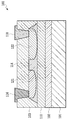
- FIG. 1 is a diagram schematically showing the structure of a conventional waveguide coupled vertical GePD.
- 2 is a sectional view taken along line II-II of FIG.
- the upper cladding layer 103 and the electrodes 116 to 118 shown in FIG. 2 are omitted, and the electrodes 116 to 118 are implanted with the first impurity and the silicon electrode portions 112, 113 and The electrodes 116 to 118 are shown as squares only at positions in contact with the Ge region 115 into which the second impurity has been implanted.
- GePD is formed on a SOI (Silicon On Insulator) substrate including a Si substrate, a Si oxide film, and a surface Si layer by using a lithography technique or the like.
- the GePD 100 shown in FIG. 2 includes a Si substrate 101, a lower cladding layer 102 including a Si oxide film on the Si substrate, a core layer 110 that guides signal light, and a Ge that absorbs light formed on the core layer 110.
- the layer 114 and the upper clad layer 103 formed on the core layer 110 and the Ge layer 114 are provided.
- the core layer 110 is divided into a waveguide layer 1101 and a silicon slab 1102.
- the silicon slab 1102 is formed with a Si slab 111 into which a first impurity is implanted, and silicon electrode portions 112 and 113 that are doped with the first impurity at a high concentration and that act as electrodes.
- the Ge layer 114 is stacked by epitaxial growth, and the Ge region 115 doped with the second impurity is formed on the top thereof.
- Reference numeral 114 may include a germanium compound. Then, electrodes 116 to 118 are provided on the silicon electrode portions 112 and 113 and the Ge region 115 so as to contact them.
- the lateral Ge PD shown in FIG. 3 includes a p-type Si slab 111 doped with a first impurity, a germanium region 121 doped with a first impurity and a second impurity instead of a Ge region 115 doped with a second impurity.
- the lateral Ge PD of FIG. 4 has a p-type Si slab 111 doped with a first impurity, a silicon region 131 doped with a first impurity and a second impurity instead of the Ge region 115 doped with a second impurity.
- the region 123 is a region in which the first impurity and the second impurity are not introduced.
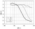
- FIG. 5 is a diagram in which the sensitivity in the reverse wavelength of 1.6 V is plotted against the temperature in the communication wavelength bands C and L bands (wavelengths 1530 to 1565 nm, 1565 to 1625 nm) of GePD.
- C and L bands wavelengths 1530 to 1565 nm, 1565 to 1625 nm
- the sensitivity is almost constant up to the C band, but the sensitivity decreases at the L band. This change in sensitivity is caused by a change in the optical absorption spectrum of germanium.
- ⁇ 5° C. sensitivity tends to decrease even in the C band.
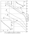
- Non-Patent Document 1 shows the temperature dependence of the light absorption spectrum of germanium (Non-Patent Document 1).
- the horizontal axis and the vertical axis represent the photon energy and the square root of the absorption coefficient k, respectively.
- the band gap of germanium shifts to the high energy side. That is, the light absorption spectrum edge shifts to the short wavelength side.
- the edge of the optical absorption spectrum of germanium used for GePD is 31° C., which is just around 1565 nm on the long wavelength side of the C band. Therefore, even at a temperature of 31° C., even a GePD showing a constant sensitivity in the entire C band, the sensitivity gradually decreases from the long wavelength side as the temperature decreases. This tendency is shown in FIG. 5, and the longer the wavelength, the lower the sensitivity tends to be at ⁇ 5° C., which is the lower temperature.
- Patent Documents 1, 2, and 3 Patent Documents 1, 2, and 3
- FIG. 7 shows an example of the configuration of a receiver used in the optical digital coherent communication technology.
- eight GePDs 704 are used.
- the GePD 704 having a heater eight heaters are required.
- the GePD 704 groups connected to the same optical hybrid 703 receive differential signals in pairs, and this pair is required to have uniform sensitivity.
- the local light source 701 and the polarization splitter 702 are connected to two optical hybrids 703, respectively.
- the common-mode rejection ratio will deteriorate, and the performance of the receiver will drop.
- the GePD and the heater have manufacturing variations, there is a problem that the sensitivity of each GePD varies, and this variation causes a penalty in the common-mode signal rejection ratio.
- the present invention has been made in view of such a problem, and an object of the present invention is to provide a GePD having uniform sensitivity in the C and L bands by using a heater so that deterioration of the common-mode signal rejection ratio is prevented. It is to make a receiver that does not happen due to the sensitivity of.
- the present invention is characterized by having the following configuration in order to achieve such an object.
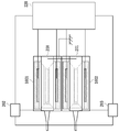
- two or more photodiodes (GePD) 1001 and 1002 arranged to receive an input differential signal, and an ammeter of a current monitor for measuring the photocurrent of the two or more photodiodes arranged.
- heaters 200, 201 which are resistors for heating the photodiodes 1001, 1002, and voltage sources 202, 203 connected to the resistors for controlling the resistors and capable of independently controlling the voltage value.
- the voltage sources 202 and 203 are connected to the ammeter 204 of the current monitor, and the voltage sources 202 and 203 are arranged so that the values of the currents output from the two or more photodiodes 1001 and 1002 from the current monitor match. In addition, it is a voltage source for operating the voltage applied to the heater.
- the GePD 1001 and the GePD 1002 are provided with a heater 200 and a heater 201, respectively.
- the heaters 200 and 201 are controlled by a power source (voltage source) 202 and a power source (voltage source) 203, and the power sources (voltage sources) 202 and 203 detect the value of the ammeter 204 and determine the voltage applied to the heater. ..
- a bias power supply is written on the cathode side of the GePDs 1001 and 1002, and a signal output terminal (output port) 212 is written on the anode side in this example, but the cathode side and the anode side may be reversed.
- the present invention it is possible to make the sensitivities of a plurality of GePDs uniform by heating the heater based on the measured value of the photocurrent by the current monitor, and to suppress the deterioration of the common-mode rejection ratio.
- FIG. 3 is a diagram showing a configuration of a photodetector of Example 1.
- FIG. 3 is a diagram showing a configuration of a photodetector of Example 1.
- FIG. 3 is a diagram showing a configuration of a photodetector of Example 1.
- FIG. 6 is a diagram showing a configuration of a photodetector of Example 2.
- FIG. 6 is a diagram showing a configuration of a photodetector of Example 3.
- FIG. 7 is a diagram showing a configuration of a photodetector of Example 4.
- the photodetector includes two or more photodiodes (GePD) 1001 and 1002 arranged to receive an input differential signal, and two or more photodiodes arranged to receive light.
- An ammeter 204 of a current monitor for measuring a current heaters 200 and 201 which are resistors for heating the photodiodes 1001 and 1002, and a voltage value independently connected to each resistor for controlling the resistor.
- the voltage sources 202 and 203 that can be controlled are connected, and the voltage sources 202 and 203 are connected to the ammeter 204 of the current monitor.
- the voltage sources 202 and 203 include two or more photodiodes 1001 and 1002 arranged from the current monitor.
- the ammeter 204 of the monitor measures the current from the GePDs 1001 and 1002.
- the monitor adjusts the voltage applied to the heater 200 and the heater 201 so that the current measured from each GePD becomes equal to each other.
- the GePD 1001 and GePD 1002 are heated by the heater to change the sensitivity. As can be seen from FIG. 5, since the sensitivity of GePD depends on the temperature, the sensitivity of a plurality of GePDs can be made uniform by heating the heater.
- the current measured by the ammeter 204 of the monitor is a photocurrent, and when these values match, it can be said that the sensitivities of the GePDs 1001 and 1002 are completely matched. On the contrary, in the photodetector of the present invention, deterioration of the in-phase signal rejection ratio cannot occur.
- Reference numeral 212 connected to the GePDs 1001 and 1002 is a signal output terminal.
- the ammeter 204 of the monitor is connected to the cathode of the GePD, but this may be connected to the anode.
- the signal output terminal 212 and the monitor ammeter 204 are connected to the anode and the cathode, respectively, the anode may have the monitor ammeter 204 and the signal output terminal 212, or the cathode may have both. You can
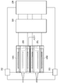
- Example 9 and 10 are a top view and a cross-sectional view, respectively, showing the configuration of this embodiment of the photodetector of the present invention.
- an ammeter connected to the cathodes of the Ge PDs 1001 and 1002 serves as a monitor, and heaters 200 and 201 containing a metal or a metal compound as resistors are arranged.
- the photodetector according to the present invention includes two or more photodiodes (GePD) 1001 and 1002 arranged to receive an input differential signal and two or more photodiodes arranged to receive light.
- Ammeters 204 and 205 of a current monitor for measuring current heaters 200 and 201 which are resistors for heating a photodiode, and voltage values which are independently connected to each resistor for controlling the resistors.
- Voltage sources 202 and 203, and the voltage sources 202 and 203 and the ammeters 204 and 205 of the current monitor are respectively connected, and the voltage sources 202 and 203 are two or more photodiodes arranged from the current monitor. It is characterized in that it is a voltage source that operates the applied voltage to the heaters 200 and 201 so that the values of the currents 1001 and 1002 are matched.
- a specific driving method is shown below.
- the heaters 200 and 201 are embedded in the upper (over) cladding layer 103 as shown in FIG.
- the GePDs 1001 and 1002 are arranged as a PD pair that receives a differential signal.
- the heaters 200 and 201 are arranged so as to cover the germanium layer 114 of each GePD.
- Ammeters 204 and 205 are provided at the cathode of each GePD, and voltage sources 206 and 207 are further connected to the ammeters 204 and 205.
- Voltage sources 202 and 203 to the heaters 200 and 201 are connected to the ammeters 204 and 205, respectively.
- the voltage sources 202 and 203 adjust the voltage applied to the heater so that the currents indicated by the ammeters 204 and 205 become equal.
- the photodiodes (GePD) 1001 and 1002 are connected to the signal output terminal 212.
- FIG. 11 is a diagram showing the configuration of this embodiment of the photodetector of the present invention.
- This is an example in which the ammeters connected to the cathodes of the GePDs 1001 and 1002 serve as monitors, and the heaters 210 and 211 made by implantation (ion implantation) are arranged on the core layers 110 of the GePDs 1001 and 1002 as resistors.
- the GePDs 1001 and 1002 are arranged as a PD pair that receives a differential signal.
- Ammeters 204 and 205 are provided at the cathode of each GePD, and voltage sources 206 and 207 are further connected to the ammeters 204 and 205.
- Voltage sources 202 and 203 to the heaters 200 and 201 are connected to the ammeters 204 and 205, respectively.
- the voltage sources 202 and 203 adjust the voltage applied to the heater so that the currents indicated by the ammeters 204 and 205 become equal.
- FIG. 12 is a diagram showing the configuration of this embodiment of the photodetector of the present invention.
- the transimpedance amplifier 220 in which the monitor is connected to the anodes of the GePDs 1001 and 1002 serves and the heaters 200 and 201 containing a metal or a metal compound as resistors are arranged.
- the GePDs 1001 and 1002 are arranged as a PD pair that receives a differential signal.
- the transimpedance amplifier 220 is an amplifier that amplifies the signal of the GePD and outputs a voltage, and at that time, monitors the current from the GePD.
- This value is fed back to the voltage sources 202 and 203, and the voltage source controls the heater so that the currents from the GePDs to the transimpedance amplifier 220 become equal.
- a heater made of a metal or a metal compound is used as the resistor in FIG. 12, a heater made by implanting (ion implantation) the core layers 110 of the Ge PDs 1001 and 1002 as shown in the second embodiment may be used.
- the anodes of the GePDs 1001 and 1002 are connected to the transimpedance amplifier 220, but the cathodes may be connected to the transimpedance amplifier 220.
- FIG. 13 is a diagram showing the configuration of this embodiment of the photodetector of the present invention.
- the digital signal processor 230 connected to the rear stage of the transimpedance amplifier 220 connected to the anodes of the GePDs 1001 and 1002 serves as a monitor, and the heaters 200 and 201 made of metal or a metal compound are arranged as resistors.
- the GePDs 1001 and 1002 are arranged as a PD pair that receives a differential signal.
- the digital signal processor 230 monitors the signal input from the GePD through the transimpedance amplifier 220, and feeds back this value to the voltage sources 202 and 203, and the voltage source makes the currents from the respective GePD into the transimpedance amplifier 220 equal.
- a heater made of a metal or a metal compound is used as the resistor in FIG. 13
- a heater made by implanting the core layers 110 of the GePDs 1001 and 1002 shown in the second embodiment may be used.
- the anodes of the GePDs 1001 and 1002 are connected to the transimpedance amplifier 220, but the cathodes may be connected.
- the present invention can be applied to a photodetector used in an optical communication system or an optical information processing system.
Landscapes
- Physics & Mathematics (AREA)
- General Physics & Mathematics (AREA)
- Spectroscopy & Molecular Physics (AREA)
- Light Receiving Elements (AREA)
- Photometry And Measurement Of Optical Pulse Characteristics (AREA)
Abstract
電流モニタでの光電流の計測値に基づくヒータの加熱によって複数のGePDの感度を揃えることができ、同相信号除去比の劣化を抑えることを課題とする。本発明の光検出器は、光吸収層にゲルマニウム、またはゲルマニウム化合物を用いたゲルマニウム光検出器(GePD)を用いた光検出器であって、入力される差動信号を受けるために2つ以上配置されたGePD(1001,1002)と、2つ以上配置されたGePDの光電流を測定する電流モニタ(204)と、GePDのそれぞれを加熱するための抵抗体(200,201)と、各抵抗体に接続された各々独立で電圧値を制御できる電圧源(202,203)とを備え、電圧源と電流モニタは接続され、電圧源は2つ以上のGePDが出す各電流値が一致するようにヒータへの印加電圧を操作することを特徴する。
Description
本発明は、光通信システムや光情報処理システムにおいて用いられる光検出器に関し、特に差動信号を受け取る時において、同相信号除去比が小さい、光検出器を提供するための構造に関するものである。
近年の光通信の普及に伴い、光通信装置の低コスト化が求められている。その解決策の1つとして、光通信装置を構成する光回路を、シリコンウエハのような大口径ウエハ上に、シリコンフォトニクスのような微小光回路技術を用いて形成する方法がある。これにより、1チップあたりの材料費を劇的に下げ、光通信装置の低コスト化を図ることが出来る。
このような技術を用いたシリコン(Si)基板上に形成する代表的な光検出器としては、モノリシック集積が可能なゲルマニウム光検出器(Germanium photodetector:GePD)がある。図1は、従来の導波路結合型の縦型GePDの構造を模式的に示す図である。図2は、図1のII-IIの断面図である。尚、構造を分かり易くするために、図1では、図2に示す上部クラッド層103、電極116~118を省き、電極116~118が第一の不純物をインプラしたシリコン電極部112、113および第二の不純物をインプラしたGe領域115に接する位置のみ四角形で電極116~118を示している。
GePDは、Si基板、Si酸化膜、及び表面Si層を備えたSOI(Silicon On Insulator)基板にリソグラフィ技術等を用いて形成される。図2に示すGePD100は、Si基板101と、Si基板上のSi酸化膜とを含む下部クラッド層102と、信号光を導くコア層110と、コア層110上に形成された光を吸収するGe層114と、コア層110およびGe層114上に形成された上部クラッド層103とを備える。図1を見るとわかるようにコア層110は導波路層1101とシリコンスラブ1102に分けられる。
シリコンスラブ1102は、第一の不純物をインプラしたSiスラブ111、および第一の不純物が高濃度にドーピングされ、電極として作用するシリコン電極部112、113が形成されている。Ge層114は、エピタキシャル成長によって積層され、その上部に第二の不純物がドーピングされたGe領域115が形成されている。符号114はゲルマニウム化合物を含んでいることもある。そして、シリコン電極部112、113およびGe領域115上には、それらに接するように電極116~118を備える。
GePDは、導波路層1101からシリコンスラブ1102に光が入射されてGe層114で光が吸収されると、電極117と電極116、118との間に光電流が流れるので、その電流を検出することで光を検出する。
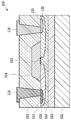
図1、2に示すGePDの他にも図3、4に示すような横型のGePDも存在する。図3の横型のGePDは第一の不純物をインプラしたp型Siスラブ111、第二の不純物がドーピングされたGe領域115の代わりに第一の不純物をインプラしたゲルマニウム領域121と第二の不純物をインプラしたゲルマニウム領域122がある。図4の横型のGePDは第一の不純物をインプラしたp型Siスラブ111、第二の不純物がドーピングされたGe領域115の代わりに第一の不純物をインプラしたシリコン領域131と第二の不純物をインプラしたシリコン領域132、第二の不純物が高濃度にドーピングされ、電極として作用するシリコン電極部113がある。符号114は、Geの代わりにゲルマニウム化合物を含んでいることもある。領域123は、第一の不純物及び第二の不純物が導入されていない領域である。
図2,3, 及び4に示すGePD100は感度(光入力パワーに対する電流出力の特性、単位A/W)の温度特性が一定ではないという特性がある。図5はGePDの通信波長帯域C、L帯(波長1530~1565nm、1565~1625nm)における温度に対する逆バイアス1.6V時における感度をプロットした図である。例えば31℃ではC帯付近まではほぼ一定の感度を示すが、L帯になると感度を落とす。この感度変化はゲルマニウムの光吸収スペクトルの変化によってもたらされている。-5℃になるとC帯においても感度を落とす傾向を示す。図6はゲルマニウムの光吸収スペクトルの温度依存性である(非特許文献1)。横軸、縦軸は、それぞれ、光子エネルギー、吸収係数kの平方根を示す。温度が低温になるとゲルマニウムのバンドギャップは高エネルギー側にシフトする。すなわち光吸収スペクトル端は短波長側にシフトする。GePDに用いているゲルマニウムの光吸収スペクトル端は31℃でちょうどC帯の長波長側の1565nm付近にある。従って31℃ではC帯全域に一定の感度を示すGePDであっても、温度が低くなるにつれ、長波長側から徐々に感度が落ちてゆく。この傾向を示したのが図5であり、長波長ほど低温である-5℃において感度を落とす傾向がある。
温度、波長によって感度が変化するGePDを光通信システムに組込もうとすると、感度変化を補償する回路が必要となるため製造コストが上がる。そのため温度依存性を解決する手段として、ヒータを設置しデバイス周りの温度を安定させる手段がある。(特許文献1,2、及び3)
一方で、GePDを用いた光通信システムや光情報処理システムでは、単独のGePDを使うことは少なく、一般に2~8個程度のGePDを並べて使う。これは多波長を使う波長分割多重方式(WDM)を採用するシステムにおいて波長の数だけGePDを必要とする場合や、光デジタルコヒーレント通信技術を採用するシステムにおいてバランスPDとして使う場合に複数のPDを必要とする。図7は光デジタルコヒーレント通信技術において用いる受信機の構成の一例である。この構成では8個のGePD704が用いられる。この時、ヒータを備えるGePD704を使った場合は8個のヒータが必要となる。特に同一の光ハイブリッド703に繋がるGePD704群は二つ一組で差動信号を受信し、このペアは均一の感度が求められる。局発光源701及び偏波分離器702は、それぞれ、二つの光ハイブリッド703に接続している。
Macfarlane G. G., T. P. McLean, J. E. Quarrington and V. Roberts, Phys. Rev. 108, 6 (1957) 1377-1383.
差動信号を受け取るGePD群は感度が均一でない場合は同相信号除去比が劣化し、受信機の性能を落とすこととなる。しかしながら、GePDやヒータは製造バラつきを持つため、各GePDの感度がバラついてしまい、このバラつきが同相信号除去比にペナルティを出すという問題が有る。
本発明はこのような問題に鑑みてなされたもので、その目的とするところは、ヒータを用いる事でC、L帯において感度の揃ったGePDを提供し、同相信号除去比の劣化がGePDの感度起因で起きない受信機を作ることにある。
本発明は、このような目的を達成するために、以下のような構成を備えることを特徴とする。図8のように、入力される差動信号を受けるため2つ以上配置されたフォトダイオード(GePD)1001,1002と、2つ以上配置されたフォトダイオードの光電流を測定する電流モニタの電流計204、フォトダイオード1001,1002を加熱するための抵抗体であるヒータ200, 201と、抵抗体を制御するため各抵抗体に接続された各々独立で電圧値を制御できる電圧源202,203とを備え、電圧源202,203と電流モニタの電流計204とは、接続され、電圧源202,203は電流モニタからの2つ以上配置されたフォトダイオード1001,1002が出す電流の値が合致するようにヒータへの印加電圧を操作する電圧源であることを特徴とする。GePD1001とGePD1002にはヒータ200とヒータ201がそれぞれ備えられる。ヒータ200とヒータ201は電源(電圧源)202と電源(電圧源)203によって制御され、この電源(電圧源)202,203は電流計204の値を検出し、ヒータに印加する電圧を決定する。GePD1001,1002のカソード側にはバイアス電源が、アノード側には信号出力用の端子(出力ポート)212が今回の例では書かれているが、カソード側とアノード側は逆転しても良い。
本発明は、電流モニタでの光電流の計測値に基づくヒータの加熱によって複数のGePDの感度を揃えることができ、同相信号除去比の劣化を抑えることができる。
以下、本発明の光検出器の形態について、好適な形態及び例を用いて詳細に説明する。なお、図面においては同一の機能を有する部分は同一の番号を付することで、説明の明瞭化を図っている。但し、本発明は以下に示す実施形態の記載内容に限定されず、本明細書等において開示する発明の趣旨から逸脱することなく形態および詳細を様々に変更し得ることは当業者にとって自明である。
本発明に係る光検出器は、図8に示す通り、入力される差動信号を受けるため2つ以上配置されたフォトダイオード(GePD)1001,1002と、2つ以上配置されたフォトダイオードの光電流を測定する電流モニタの電流計204、フォトダイオード1001,1002を加熱するための抵抗体であるヒータ200, 201と、抵抗体を制御するため各抵抗体に接続された各々独立で電圧値を制御できる電圧源202,203とを備え、電圧源202,203と電流モニタの電流計204とは接続され、電圧源202,203は電流モニタからの2つ以上配置されたフォトダイオード1001,1002が出す電流の値が合致するようにヒータへの印加電圧を操作する電圧源であることを特徴とする。具体的な駆動方法を以下に示す。モニタの電流計204がGePD1001と1002からの電流を測定する。モニタは各GePDから測定した電流がお互い等しくなるようにヒータ200とヒータ201への印加電圧を調整する。ヒータによってGePD1001とGePD1002は加熱され、感度を変化させる。図5からわかるように、GePDの感度は温度に依存するため、ヒータの加熱によって複数のGePDの感度を揃える事が出来る。モニタの電流計204が測定する電流は光電流であり、これらの値が一致するとき、GePD1001,1002の感度は完全に合致していると言える。翻って、本発明の光検出器においては同相信号除去比の劣化が起きえない。GePD1001,1002と接続する符号212は信号出力用の端子である。図8ではGePDのカソードにモニタの電流計204を繋いだが、これはアノードに繋がれても良い。また、信号出力用の端子212とモニタの電流計204はそれぞれアノードとカソードに繋いだが、アノードにモニタの電流計204と信号出力用の端子212が有っても良いし、カソードに両者が有っても良い。
(実施例1)
図9、10は、それぞれ、本発明の光検出器の本実施例の構成を示す上面図、断面図である。モニタをGePD1001と1002のカソードに接続された電流計が果たし、抵抗体として金属または金属化合物を含むヒータ200、201を配置した例である。本発明に係る光検出器は、図9に示す通り、入力される差動信号を受けるため2つ以上配置されたフォトダイオード(GePD)1001,1002と、2つ以上配置されたフォトダイオードの光電流を測定する電流モニタの電流計204, 205、フォトダイオードを加熱するための抵抗体であるヒータ200, 201と、抵抗体を制御するため各抵抗体に接続された各々独立で電圧値を制御できる電圧源202,203とを備え、電圧源202,203と電流モニタの電流計204, 205とは、それぞれ、接続され、電圧源202,203は電流モニタからの2つ以上配置されたフォトダイオード1001,1002が出す電流の値が合致するようにヒータ200, 201への印加電圧を操作する電圧源であることを特徴とする。具体的な駆動方法を以下に示す。ヒータ200, 201は図10の様に上部(オーバー)クラッド層103の中に埋め込まれる。GePD1001,1002は差動信号を受けるPDペアとして配置してある。ヒータ200,201は各GePDのゲルマニウム層114を覆うように配置される。各GePDのカソードには電流計204,205が有り、さらにその先に電圧源206,207が接続されている。電流計204,205には各々ヒータ200,201への電圧源202、203が接続されている。電圧源202,203は電流計204,205の示す電流が等しくなるようにヒータに掛ける電圧を調整する。フォトダイオード(GePD)1001,1002は、信号出力用の端子212と接続する。
図9、10は、それぞれ、本発明の光検出器の本実施例の構成を示す上面図、断面図である。モニタをGePD1001と1002のカソードに接続された電流計が果たし、抵抗体として金属または金属化合物を含むヒータ200、201を配置した例である。本発明に係る光検出器は、図9に示す通り、入力される差動信号を受けるため2つ以上配置されたフォトダイオード(GePD)1001,1002と、2つ以上配置されたフォトダイオードの光電流を測定する電流モニタの電流計204, 205、フォトダイオードを加熱するための抵抗体であるヒータ200, 201と、抵抗体を制御するため各抵抗体に接続された各々独立で電圧値を制御できる電圧源202,203とを備え、電圧源202,203と電流モニタの電流計204, 205とは、それぞれ、接続され、電圧源202,203は電流モニタからの2つ以上配置されたフォトダイオード1001,1002が出す電流の値が合致するようにヒータ200, 201への印加電圧を操作する電圧源であることを特徴とする。具体的な駆動方法を以下に示す。ヒータ200, 201は図10の様に上部(オーバー)クラッド層103の中に埋め込まれる。GePD1001,1002は差動信号を受けるPDペアとして配置してある。ヒータ200,201は各GePDのゲルマニウム層114を覆うように配置される。各GePDのカソードには電流計204,205が有り、さらにその先に電圧源206,207が接続されている。電流計204,205には各々ヒータ200,201への電圧源202、203が接続されている。電圧源202,203は電流計204,205の示す電流が等しくなるようにヒータに掛ける電圧を調整する。フォトダイオード(GePD)1001,1002は、信号出力用の端子212と接続する。
(実施例2)
図11は本発明の光検出器の本実施例の構成を示す図である。モニタをGePD1001と1002のカソードに接続された電流計が果たし、抵抗体としてGePD1001と1002のコア層110にインプラ(イオン注入)で作製したヒータ210、211を配置した例である。GePD1001,1002は差動信号を受けるPDペアとして配置してある。各GePDのカソードには電流計204,205が有り、さらにその先に電圧源206,207が接続されている。電流計204,205には各々ヒータ200,201への電圧源202、203が接続されている。電圧源202,203は電流計204,205の示す電流が等しくなるようにヒータに掛ける電圧を調整する。
図11は本発明の光検出器の本実施例の構成を示す図である。モニタをGePD1001と1002のカソードに接続された電流計が果たし、抵抗体としてGePD1001と1002のコア層110にインプラ(イオン注入)で作製したヒータ210、211を配置した例である。GePD1001,1002は差動信号を受けるPDペアとして配置してある。各GePDのカソードには電流計204,205が有り、さらにその先に電圧源206,207が接続されている。電流計204,205には各々ヒータ200,201への電圧源202、203が接続されている。電圧源202,203は電流計204,205の示す電流が等しくなるようにヒータに掛ける電圧を調整する。
(実施例3)
図12は本発明の光検出器の本実施例の構成を示す図である。モニタをGePD1001と1002のアノードに接続したトランスインピーダンスアンプ220が果たし、抵抗体として金属または金属化合物を含むヒータ200、201を配置した例である。GePD1001,1002は差動信号を受けるPDペアとして配置してある。トランスインピーダンスアンプ220はGePDの信号を増幅して電圧出力するアンプであり、その際にGePDからの電流をモニタする。この値を電圧源202,203にフィードバックし、電圧源は各GePDからトランスインピーダンスアンプ220に入る電流が等しくなるようにヒータを制御する。図12では抵抗体として金属または金属化合物によるヒータを用いたが、実施例2に示すようにGePD1001と1002のコア層110にインプラ(イオン注入)をして作ったヒータを用いても良い。また図12ではGePD1001,1002のアノードからトランスインピーダンスアンプ220に接続しているが、カソードからトランスインピーダンスアンプ220に接続しても良い。
図12は本発明の光検出器の本実施例の構成を示す図である。モニタをGePD1001と1002のアノードに接続したトランスインピーダンスアンプ220が果たし、抵抗体として金属または金属化合物を含むヒータ200、201を配置した例である。GePD1001,1002は差動信号を受けるPDペアとして配置してある。トランスインピーダンスアンプ220はGePDの信号を増幅して電圧出力するアンプであり、その際にGePDからの電流をモニタする。この値を電圧源202,203にフィードバックし、電圧源は各GePDからトランスインピーダンスアンプ220に入る電流が等しくなるようにヒータを制御する。図12では抵抗体として金属または金属化合物によるヒータを用いたが、実施例2に示すようにGePD1001と1002のコア層110にインプラ(イオン注入)をして作ったヒータを用いても良い。また図12ではGePD1001,1002のアノードからトランスインピーダンスアンプ220に接続しているが、カソードからトランスインピーダンスアンプ220に接続しても良い。
(実施例4)
図13は本発明の光検出器の本実施例の構成を示す図である。モニタをGePD1001と1002のアノードに接続したトランスインピーダンスアンプ220の後段に接続するデジタルシグナルプロセッサ230が果たし、抵抗体として金属または金属化合物によるヒータ200、201を配置した例である。GePD1001,1002は差動信号を受けるPDペアとして配置してある。デジタルシグナルプロセッサ230はトランスインピーダンスアンプ220を通してGePDから入力される信号をモニタしており、この値を電圧源202,203にフィードバックし、電圧源は各GePDからトランスインピーダンスアンプ220に入る電流が等しくなるようにヒータを制御する。図13では抵抗体として金属または金属化合物によるヒータを用いたが、実施例2で示したGePD1001と1002のコア層110にインプラをして作ったヒータを用いても良い。また図12ではGePD1001,1002のアノードからトランスインピーダンスアンプ220に接続しているが、カソードから接続しても良い。
図13は本発明の光検出器の本実施例の構成を示す図である。モニタをGePD1001と1002のアノードに接続したトランスインピーダンスアンプ220の後段に接続するデジタルシグナルプロセッサ230が果たし、抵抗体として金属または金属化合物によるヒータ200、201を配置した例である。GePD1001,1002は差動信号を受けるPDペアとして配置してある。デジタルシグナルプロセッサ230はトランスインピーダンスアンプ220を通してGePDから入力される信号をモニタしており、この値を電圧源202,203にフィードバックし、電圧源は各GePDからトランスインピーダンスアンプ220に入る電流が等しくなるようにヒータを制御する。図13では抵抗体として金属または金属化合物によるヒータを用いたが、実施例2で示したGePD1001と1002のコア層110にインプラをして作ったヒータを用いても良い。また図12ではGePD1001,1002のアノードからトランスインピーダンスアンプ220に接続しているが、カソードから接続しても良い。
本発明は、光通信システムや光情報処理システムにおいて用いられる光検出器に適用することができる。
200,201 ヒータ
202,203 電源(電圧源)
204 電流計
212 出力ポート
1001,1002 GePD
202,203 電源(電圧源)
204 電流計
212 出力ポート
1001,1002 GePD
Claims (8)
- 入力される差動信号を受けるため2つ以上配置されたフォトダイオードと、
前記2つ以上配置されたフォトダイオードの光電流を測定する電流モニタと、
前記フォトダイオードを加熱するための抵抗体と、
前記抵抗体を制御するため各抵抗体に接続された各々独立で電圧値を制御できる電圧源とを備え、
前記電圧源と前記電流モニタは接続され、前記電圧源は前記電流モニタからの前記2つ以上配置されたフォトダイオードが出す電流の値が合致するように前記抵抗体への印加電圧を操作する電圧源である、
ことを特徴とする光検出器。 - 前記フォトダイオードは
シリコン基板と、
前記シリコン基板上の下部クラッド層と、
前記下部クラッド層上にあり、第一の導電型不純物イオンがドーピングされたシリコン領域を含むシリコンコア層と、
前記シリコンコア層上にあり、第二の導電型不純物がドーピングされたゲルマニウム領域を含むゲルマニウム層と、
前記シリコンコア層および前記ゲルマニウム層上にある上部クラッド層と、
前記シリコン領域および前記ゲルマニウム領域にそれぞれ接続された電極とを備える、
ことを特徴とする請求項1に記載の光検出器。 - 前記フォトダイオードは
シリコン基板と、
前記シリコン基板上の下部クラッド層と、
前記下部クラッド層上のシリコンコア層と、
前記シリコンコア層上にあり、第一の導電型不純物及び第二の導電型不純物がドーピングされたゲルマニウム領域を含むゲルマニウム層と、
前記シリコンコア層および前記ゲルマニウム層上の上部クラッド層と、
前記第一の導電型不純物及び第二の導電型不純物がドーピングされたゲルマニウム領域にそれぞれ接続された電極とを備える、
ことを特徴とする請求項1に記載の光検出器。 - 前記フォトダイオードは
シリコン基板と、
前記シリコン基板上に形成された下部クラッド層と、
前記下部クラッド層上に形成され、第一と第二の導電型不純物イオンがドーピングされたシリコン領域を含むシリコンコア層と、
前記シリコンコア層上に形成されたゲルマニウム層と、
前記シリコンコア層および前記ゲルマニウム層上に形成された上部クラッド層と、
前記シリコン領域に接続された電極を備える、
ことを特徴とする請求項1に記載の光検出器。 - 前記抵抗体は前記ゲルマニウム層を覆うように、前記上部クラッド層に埋め込まれた、金属または金属化合物を含む抵抗体である
ことを特徴とする請求項2乃至4いずれか一項に記載の光検出器。 - 前記抵抗体は前記ゲルマニウム層を囲うように、前記シリコンコア層に不純物イオンを含む抵抗体である
ことを特徴とする請求項2乃至4いずれか一項に記載の光検出器。 - 前記電流モニタは、前記フォトダイオードのアノードまたはカソードに接続された電流計である、
ことを特徴とする請求項1に記載の光検出器。 - 前記電流モニタは、前記フォトダイオードのアノードまたはカソードに接続されたトランスインピーダンスアンプまたはデジタルシグナルプロセッサである、
ことを特徴とする請求項1に記載の光検出器。
Priority Applications (1)
| Application Number | Priority Date | Filing Date | Title |
|---|---|---|---|
| US17/420,644 US12087800B2 (en) | 2019-01-16 | 2020-01-14 | Photodector including germanium layer and doped region |
Applications Claiming Priority (2)
| Application Number | Priority Date | Filing Date | Title |
|---|---|---|---|
| JP2019-005535 | 2019-01-16 | ||
| JP2019005535A JP7088037B2 (ja) | 2019-01-16 | 2019-01-16 | 光検出器 |
Publications (1)
| Publication Number | Publication Date |
|---|---|
| WO2020149266A1 true WO2020149266A1 (ja) | 2020-07-23 |
Family
ID=71613538
Family Applications (1)
| Application Number | Title | Priority Date | Filing Date |
|---|---|---|---|
| PCT/JP2020/000917 Ceased WO2020149266A1 (ja) | 2019-01-16 | 2020-01-14 | 光検出器 |
Country Status (3)
| Country | Link |
|---|---|
| US (1) | US12087800B2 (ja) |
| JP (1) | JP7088037B2 (ja) |
| WO (1) | WO2020149266A1 (ja) |
Citations (4)
| Publication number | Priority date | Publication date | Assignee | Title |
|---|---|---|---|---|
| WO2014156336A1 (ja) * | 2013-03-27 | 2014-10-02 | 日本電気株式会社 | 光受信回路 |
| US20150243800A1 (en) * | 2014-02-21 | 2015-08-27 | Sifotonics Technologies Co., Ltd. | Ge/Si Avalanche Photodiode With Integrated Heater And Fabrication Thereof |
| JP2018074104A (ja) * | 2016-11-04 | 2018-05-10 | 日本電信電話株式会社 | 光検出器 |
| JP2018082089A (ja) * | 2016-11-17 | 2018-05-24 | 日本電信電話株式会社 | 光検出器 |
Family Cites Families (10)
| Publication number | Priority date | Publication date | Assignee | Title |
|---|---|---|---|---|
| JP2000221455A (ja) | 1999-02-03 | 2000-08-11 | Hitachi Cable Ltd | 導波路型光モジュール |
| US7189951B2 (en) * | 2002-04-09 | 2007-03-13 | Canon Kabushiki Kaisha | Solid-state image sensing apparatus and image sensing system |
| JP4945907B2 (ja) | 2005-03-03 | 2012-06-06 | 日本電気株式会社 | 波長可変レーザ |
| US8232516B2 (en) * | 2009-07-31 | 2012-07-31 | International Business Machines Corporation | Avalanche impact ionization amplification devices |
| DE102010043822B4 (de) * | 2010-11-12 | 2014-02-13 | Namlab Ggmbh | Fotodiode und Fotodiodenfeld sowie Verfahren zu deren Betrieb |
| KR102058605B1 (ko) * | 2012-12-11 | 2019-12-23 | 삼성전자주식회사 | 광 검출기 및 이를 포함하는 이미지 센서 |
| US9755096B2 (en) * | 2014-03-10 | 2017-09-05 | Elenion Technologies, Llc | Lateral Ge/Si avalanche photodetector |
| US9871153B2 (en) * | 2015-09-24 | 2018-01-16 | Elenion Technologies, Inc. | Photodetector with integrated temperature control element formed at least in part in a semiconductor layer |
| US10418407B2 (en) * | 2015-11-06 | 2019-09-17 | Artilux, Inc. | High-speed light sensing apparatus III |
| JP6660338B2 (ja) * | 2017-04-04 | 2020-03-11 | 日本電信電話株式会社 | 光検出器 |
-
2019
- 2019-01-16 JP JP2019005535A patent/JP7088037B2/ja active Active
-
2020
- 2020-01-14 US US17/420,644 patent/US12087800B2/en active Active
- 2020-01-14 WO PCT/JP2020/000917 patent/WO2020149266A1/ja not_active Ceased
Patent Citations (4)
| Publication number | Priority date | Publication date | Assignee | Title |
|---|---|---|---|---|
| WO2014156336A1 (ja) * | 2013-03-27 | 2014-10-02 | 日本電気株式会社 | 光受信回路 |
| US20150243800A1 (en) * | 2014-02-21 | 2015-08-27 | Sifotonics Technologies Co., Ltd. | Ge/Si Avalanche Photodiode With Integrated Heater And Fabrication Thereof |
| JP2018074104A (ja) * | 2016-11-04 | 2018-05-10 | 日本電信電話株式会社 | 光検出器 |
| JP2018082089A (ja) * | 2016-11-17 | 2018-05-24 | 日本電信電話株式会社 | 光検出器 |
Also Published As
| Publication number | Publication date |
|---|---|
| US20220077219A1 (en) | 2022-03-10 |
| US12087800B2 (en) | 2024-09-10 |
| JP7088037B2 (ja) | 2022-06-21 |
| JP2020113720A (ja) | 2020-07-27 |
Similar Documents
| Publication | Publication Date | Title |
|---|---|---|
| Masini et al. | A four-channel, 10Gbps monolithic optical receiver in 130nm CMOS with integrated Ge waveguide photodetectors | |
| US20100054761A1 (en) | Monolithic coherent optical detectors | |
| US6731424B1 (en) | Dynamic gain flattening in an optical communication system | |
| WO2010021669A2 (en) | Monolithic coherent optical detectors | |
| JP6646559B2 (ja) | 光検出器 | |
| US10446699B2 (en) | Germanium photodetector with extended responsivity | |
| US12057518B2 (en) | Avalanche photodiodes with lower excess noise and lower bandwidth variation | |
| WO2017023301A1 (en) | Lateral ge/si avalanche photodetector | |
| US11769849B2 (en) | Photodetector | |
| US11543293B2 (en) | Photodetector | |
| JP7088037B2 (ja) | 光検出器 | |
| US11887999B2 (en) | Photodetector | |
| JP6660338B2 (ja) | 光検出器 | |
| CN111543017B (zh) | 平衡半导体光波导中的损耗 | |
| US12119419B2 (en) | Photodetector | |
| US20260110861A1 (en) | Structure for polarization-independent coarse wavelength division demultiplexing | |
| JP2000183320A (ja) | 受光装置 | |
| JP7081508B2 (ja) | 光検出器 | |
| Colace et al. | Optical power monitors in Ge monolithically integrated on SOI chips | |
| KR19980030013A (ko) | 모니터용 광검출기 일체형 광출력장치 | |
| JPH02119273A (ja) | 半導体受光素子 |
Legal Events
| Date | Code | Title | Description |
|---|---|---|---|
| 121 | Ep: the epo has been informed by wipo that ep was designated in this application |
Ref document number: 20741636 Country of ref document: EP Kind code of ref document: A1 |
|
| NENP | Non-entry into the national phase |
Ref country code: DE |
|
| 122 | Ep: pct application non-entry in european phase |
Ref document number: 20741636 Country of ref document: EP Kind code of ref document: A1 |