WO2020149197A1 - 情報処理装置および情報処理方法 - Google Patents
情報処理装置および情報処理方法 Download PDFInfo
- Publication number
- WO2020149197A1 WO2020149197A1 PCT/JP2020/000335 JP2020000335W WO2020149197A1 WO 2020149197 A1 WO2020149197 A1 WO 2020149197A1 JP 2020000335 W JP2020000335 W JP 2020000335W WO 2020149197 A1 WO2020149197 A1 WO 2020149197A1
- Authority
- WO
- WIPO (PCT)
- Prior art keywords
- information
- identifier
- processing unit
- processing
- held
- Prior art date
- Legal status (The legal status is an assumption and is not a legal conclusion. Google has not performed a legal analysis and makes no representation as to the accuracy of the status listed.)
- Ceased
Links
Images


Classifications
-
- G—PHYSICS
- G06—COMPUTING OR CALCULATING; COUNTING
- G06F—ELECTRIC DIGITAL DATA PROCESSING
- G06F11/00—Error detection; Error correction; Monitoring
- G06F11/07—Responding to the occurrence of a fault, e.g. fault tolerance
- G06F11/0703—Error or fault processing not based on redundancy, i.e. by taking additional measures to deal with the error or fault not making use of redundancy in operation, in hardware, or in data representation
- G06F11/0751—Error or fault detection not based on redundancy
- G06F11/0763—Error or fault detection not based on redundancy by bit configuration check, e.g. of formats or tags
-
- G—PHYSICS
- G06—COMPUTING OR CALCULATING; COUNTING
- G06F—ELECTRIC DIGITAL DATA PROCESSING
- G06F11/00—Error detection; Error correction; Monitoring
- G06F11/07—Responding to the occurrence of a fault, e.g. fault tolerance
- G06F11/0703—Error or fault processing not based on redundancy, i.e. by taking additional measures to deal with the error or fault not making use of redundancy in operation, in hardware, or in data representation
- G06F11/0706—Error or fault processing not based on redundancy, i.e. by taking additional measures to deal with the error or fault not making use of redundancy in operation, in hardware, or in data representation the processing taking place on a specific hardware platform or in a specific software environment
- G06F11/073—Error or fault processing not based on redundancy, i.e. by taking additional measures to deal with the error or fault not making use of redundancy in operation, in hardware, or in data representation the processing taking place on a specific hardware platform or in a specific software environment in a memory management context, e.g. virtual memory or cache management
-
- G—PHYSICS
- G06—COMPUTING OR CALCULATING; COUNTING
- G06F—ELECTRIC DIGITAL DATA PROCESSING
- G06F11/00—Error detection; Error correction; Monitoring
- G06F11/07—Responding to the occurrence of a fault, e.g. fault tolerance
- G06F11/16—Error detection or correction of the data by redundancy in hardware
- G06F11/1666—Error detection or correction of the data by redundancy in hardware where the redundant component is memory or memory area
- G06F11/167—Error detection by comparing the memory output
-
- G—PHYSICS
- G06—COMPUTING OR CALCULATING; COUNTING
- G06F—ELECTRIC DIGITAL DATA PROCESSING
- G06F15/00—Digital computers in general; Data processing equipment in general
- G06F15/76—Architectures of general purpose stored program computers
- G06F15/78—Architectures of general purpose stored program computers comprising a single central processing unit
-
- G—PHYSICS
- G06—COMPUTING OR CALCULATING; COUNTING
- G06F—ELECTRIC DIGITAL DATA PROCESSING
- G06F11/00—Error detection; Error correction; Monitoring
- G06F11/07—Responding to the occurrence of a fault, e.g. fault tolerance
- G06F11/0703—Error or fault processing not based on redundancy, i.e. by taking additional measures to deal with the error or fault not making use of redundancy in operation, in hardware, or in data representation
- G06F11/0766—Error or fault reporting or storing
- G06F11/0784—Routing of error reports, e.g. with a specific transmission path or data flow
-
- G—PHYSICS
- G06—COMPUTING OR CALCULATING; COUNTING
- G06F—ELECTRIC DIGITAL DATA PROCESSING
- G06F11/00—Error detection; Error correction; Monitoring
- G06F11/07—Responding to the occurrence of a fault, e.g. fault tolerance
- G06F11/0703—Error or fault processing not based on redundancy, i.e. by taking additional measures to deal with the error or fault not making use of redundancy in operation, in hardware, or in data representation
- G06F11/0793—Remedial or corrective actions
Definitions
- the present invention relates to an information processing device and an information processing method.
- Some conventional information processing devices include one processing unit, and the processing unit processes a plurality of information.
- Such an information processing apparatus includes a plurality of input memories and a plurality of output memories in order to process a plurality of information.
- the information processing device processes information for 1024 channels (“ch” is an abbreviation for channel)
- the information processing device includes an input memory for 1024 channels and an output memory for 1024 channels.
- Non-Patent Document 1 Digital Signal Processor
- an object of the present invention is to detect a failure of a processing unit that processes a plurality of information in a short time.
- the invention according to claim 1 is an information processing apparatus including a processing unit that processes a plurality of information, and an identifier adding unit that adds an identifier to each of the plurality of information, A plurality of input memories each holding each of the plurality of information and each of the identifiers added to the plurality of information, each of the plurality of information processed by the processing unit, and the processing Comparing a plurality of output memories holding each of the identifiers added to the plurality of completed information and an identifier held in each of the output memories with an identifier held in each of the input memories And an identifier visa section for visa verification.
- the invention according to claim 3 is an information processing method in an information processing apparatus including a processing unit that processes a plurality of information, wherein the information processing apparatus adds an identifier to each of the plurality of information. And each of the plurality of information, and a step of retaining each of the identifiers added to the plurality of information in a plurality of input memory, each of the plurality of information processed by the processing unit, And holding each of the identifiers added to the processed plurality of information in a plurality of output memories, and holding the identifier held in each of the output memories in each of the input memories Performing the step of visa comparing with the registered identifier.
- the output memory by checking the identifier held in the output memory, whether or not the information added by the identifier is the target information, that is, the output memory It is possible to reliably determine whether or not the information is to be retained in the. Therefore, the failure of the processing unit that processes a plurality of information can be found in a short time.
- the invention according to claim 2 is the information processing apparatus according to claim 1, wherein an identifier held in a specific output memory among the plurality of output memories is determined by the visa. It further comprises an error processing unit for performing error processing when the identifier held in the specific input memory corresponding to the output memory does not match.
- the invention according to claim 4 is the information processing method according to claim 3, wherein the information processing device is held in a specific output memory among the plurality of output memories by the visa. If the identifier does not match the identifier held in the specific input memory corresponding to the specific output memory, the step of performing error processing is further executed.
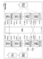
- the information processing apparatus 100 of this embodiment includes a processing unit 1, input memories 20000 to 21023, output memories 30000 to 31023, an identifier adding unit 2, an identifier visa unit 3, and an error handling unit. And part 4.
- the information processing apparatus 100 will be described as processing information for 1024 channels.
- the processing unit 1 processes a plurality of information.
- the information processing apparatus 100 will be described as including one processing unit 1, but the present invention can also be applied to a case where the information processing apparatus 100 includes a plurality of processing units 1.
- the processing unit 1 can be, for example, a microcomputer or a DSP, but is not limited to these. Further, the processing by the processing unit 1 can be, for example, echo cancellation, codec conversion, and band compression, but is not limited to these.
- the input memories 20000 to 21023 hold information 40000 to 41023 for 1024 channels input to the information processing apparatus 100, respectively.
- Information 40000 to 41023 is information before processing by the processing unit 1.
- the information 40000 to 41023 can be, for example, audio, but is not limited thereto.
- the output memories 30000 to 31023 hold information 50000 to 51023 for 1024 channels output from the information processing apparatus 100 to a receiver (not shown), respectively.
- Information 50000 to 51023 is information that has been processed by the processing unit 1.
- the information 50000 to 51023 can be, for example, audio, but is not limited thereto.
- the identifier adding unit 2 adds, to the information 40000 to 41023, identifiers 60000 to 61023 for identifying each of the information 40000 to 41023.
- the identifiers 60000 to 61023 can be, for example, 10-bit binary data, but are not limited to this.
- the input memories 20000 to 21023 each have an area for holding information 40000 to 41023 and an area for holding identifiers 60000 to 61023, and hold information 40000 to 41023 and identifiers 60000 to 61023.
- the processing unit 1 When reading the N-th information from the N-th input memory, the processing unit 1 also reads the identifier attached to the N-th information. When processing the N-th information, the processing unit 1 does not change the identifier added to the N-th information and keeps it. The processing unit 1 writes the processed Nch-th information and the identifier added to the processed Nch-th information to the Nch-th output memory.
- the output memories 30000 to 31023 each have an area for holding processed information 50000 to 51023 and an area for holding identifiers 70000 to 71023 added to the information 50000 to 51023. It also holds the identifiers 70000 to 71023.
- the identifier visa unit 3 compares the identifiers 70000 to 71023 held in the output memories 30000 to 31023 with the identifiers 60000 to 61023 held in the input memories 20000 to 21023, respectively. Specifically, the identifier visa unit 3 reads the identifier added to the processed Nch information from the Nch output memory, and the read identifier is stored in the Nch input memory (corresponding input memory). It is determined whether or not it matches the stored identifier of the N-th information before processing. The identifier visa unit 3 knows in which of the input memories 20000 to 21023 each of the identifiers added by the identifier adding unit 2 is stored.
- the error processing unit 4 performs error processing when the identifiers 70000 to 71023 and the identifiers 60000 to 61023 do not match as a result of the visa of the identifiers 70000 to 71023 by the identifier visa unit 3. Specifically, the identifier added to the processed Nch information read from the Nch output memory is added to the unprocessed Nch information held in the Nch input memory. If the identifier does not match the existing identifier, the error processing unit 4 determines that the processing unit 1 is out of order and executes error processing.
- the error processing may be, for example, notifying the maintenance person or discarding information in which the identifiers do not match, but is not limited thereto.
- the 1022th channel information 41022 held in the 1022nd channel input memory 21022 shown in FIG. 1 and the identifier 61022 added to the information 41022 and having the value “1111111110” and the 1023th channel input memory A description will be given of an operation example of information 41023 of the 1023th channel held in 21023 and an identifier 61023 added to the information 41023 and having a value of “1111111111”.
- the processing unit 1 When the processing unit 1 is normal, the processing unit 1 reads the information 41022 of the 1022nd channel and the identifier 61022 from the input memory 21022 of the 1022nd channel and processes them. After processing, the processing unit 1 writes the processed information 51022 on the 1022nd channel and the identifier 71022 that has not been changed from the value “1111111110” to the output memory 31022 on the 1022nd channel.
- the identifier visa unit 3 reads the identifier 71022 added to the processed information 51022 of the 1022nd channel from the output memory 31022 of the 1022nd channel, and the information of the 1022nd channel before processing stored in the input memory 21022 of the 1022nd channel.
- the processing unit 1 determines that the processing unit 1 is normal. Further, it is determined that the processed 1022 ch information 51022 held in the 1022 ch output memory 31022 corresponds to the unprocessed 1022 ch information 41022 held in the 1022 ch input memory 21022. ..
- the processing unit 1 reads the 1023th channel information 41023 and the identifier 61023 from the 1023th channel input memory 21023 and processes them. After the processing, the processing unit 1 writes the processed information 1023ch for channel 1023ch and the identifier 71023 that has not been changed from the value “1111111111” to the output memory 31023 for channel 1023.
- the identifier visa unit 3 reads the identifier 71023 added to the processed information 1023ch for channel 1023 from the output memory 31023 for channel 1023, and the information for channel 1023 before processing stored in the input memory 21023 for channel 1023. It is determined whether or not it matches the identifier 61023 added to the.
- the identifiers 71023 and 61023 match with each other with a value of “1111111111”, and therefore the processing unit 1 determines that the processing unit 1 is normal.
- the processed 1023 ch information 51023 held in the 1023 ch output memory 31023 corresponds to the unprocessed 1023 ch information 41023 held in the 1023 ch input memory 21023. ..
- an identifier having a value of “1111111111” is added to the processed information 1023ch of the 1023nd channel and the information 51023 in the output memory 31022 of the 1022nd channel. It is assumed that 71023 has been held.
- the identifier visa unit 3 visa the identifier 71023 read from the output memory 31022 of the 1022nd channel.
- the value of “1111111111” possessed by the identifier 71023 read from the output memory 31022 of the 1022nd channel is stored in the input memory 21022 of the 1022nd channel and is added to the information 41022 of the 1022nd channel before processing 61022.
- the identifier visa unit 3 determines that the processing unit 1 is out of order. In addition, it is determined that the processed 1023 ch information 51023 held in the 1022 ch output memory 31022 does not correspond to the unprocessed 1022 ch information 41022 held in the 1022 ch input memory 21022. .. Therefore, the error processing unit 4 performs an error process on the processed information 1023ch of 1023th channel held in the output memory 31022 of 1022nd channel.
- the processed information 51022 on the 1022nd channel and the identifier 71022 having the value of “1111111110” are added to the processed information 51022 on the 1022nd channel and the information 51022.
- the identifier visa unit 3 visa the identifier 71022 read from the output memory 31023 of the 1023th channel.
- the value of “1111111110” of the identifier 71022 read from the output memory 31023 of the 1023th channel is held in the input memory 21023 of the 1023th channel and is added to the information 41023 of the 1023th channel before processing 61023. It does not match the value of "1111111111” held by.
- the identifier visa unit 3 determines that the processing unit 1 is out of order. Further, it is determined that the processed information 1022ch of 1022th held in the output memory 31023 of 1023th channel does not correspond to the information 41023 of 1023th channel before processing held in the input memory 21023 of 1023th channel. .. Therefore, the error processing unit 4 performs error processing on the processed information 51022 on the 1022th channel held in the output memory 31023 on the 1023th channel.
- the identifier adding unit 2 adds an individual identifier to each of the 1024 channels of information (step S1).
- the information processing apparatus 100 holds information for 1024 channels and an identifier added to each information in the input memories 20000 to 21023 for 1024 channels (step S2).
- the information processing apparatus 100 causes the processing unit 1 to read the information and the identifier from the input memories 20000 to 21023 and process the information (step S3). At this time, the processing unit 1 does not change the identifier.
- the information processing apparatus 100 causes the processing unit 1 to write the processed information for 1024 channels and the identifier added to the processed information to the output memory (step S4). At this time, the processing unit 1 writes the processed information of the Nth channel and the identifier added to the processed information to the output memory of the Nth channel.
- the information processing apparatus 100 causes the identifier visa unit 3 to visa the identifier held in the Nth output memory (step S6).
- the identifier visa unit 3 determines whether the identifier held in the output memory of the Nth channel, which is the visa object, matches the identifier held in the input memory of the Nth channel. The determination is made (step S7).
- step S7 the information processing apparatus 100 causes the identifier visa unit 3 to determine that the processing unit 1 is normal. After that, the information processing device 100 performs a loop process for the next identifier.
- the information processing apparatus 100 causes the identifier visa unit 3 to determine that the processing unit 1 has a failure. In this case, the information processing apparatus 100 causes the error processing unit 4 to perform error processing on the processed Nchth information held in the Nchth output memory (step S8). After that, the information processing device 100 performs a loop process for the next identifier. When the loop process is executed for all N, the process of the information processing device 100 ends.
- the present embodiment by validating the identifier held in the output memory, whether or not the information added by the identifier is the target information, that is, the information to be held in the output memory. It is possible to reliably determine whether or not Therefore, the failure of the processing unit 1 that processes a plurality of information can be found in a short time. Further, it is possible to provide a coping means when a failure of the processing unit 1 is found.
- the information processing apparatus 100 causes the error processing unit 4 to perform error processing on the processed Nchth information held in the Nchth output memory (step S8 in FIG. 3). reference).
- the error processing unit 4 may perform error processing for the information processing apparatus 100 as a whole when the identifiers do not match even for 1ch. It is also possible to realize a technique in which various techniques described in the present embodiment are appropriately combined.
- processing unit 2 identifier adding unit 3 identifier visa unit 4 error processing unit 20000 to 21023 input memory 30000 to 31023 output memory 40000 to 41023 (before processing) information 50000 to 51023 (processed) information 60000 to 61023 Identifier (held in input memory) 70000-71023 Identifier (held in output memory)
Landscapes
- Engineering & Computer Science (AREA)
- Theoretical Computer Science (AREA)
- Physics & Mathematics (AREA)
- General Engineering & Computer Science (AREA)
- General Physics & Mathematics (AREA)
- Quality & Reliability (AREA)
- Computer Hardware Design (AREA)
- Hardware Redundancy (AREA)
- Debugging And Monitoring (AREA)
- Microcomputers (AREA)
Abstract
【課題】複数の情報を処理する処理部の故障を短時間で発見する。 【解決手段】複数の情報を処理する処理部1を備える情報処理装置100は、複数の情報40000~41023の各々に識別子60000~61023を付加する識別子付加部2と、複数の情報40000~41023の各々、および、当該複数の情報40000~41023に付加された識別子60000~61023の各々を保持する複数の入力メモリ20000~21023と、処理部1によって処理済みとなった複数の情報50000~51023の各々、および、当該処理済みとなった複数の情報50000~51023に付加された識別子70000~71023の各々を保持する複数の出力メモリ30000~31023と、識別子70000~71023を識別子60000~61023と比較して査証する識別子査証部3と、識別子が一致しない場合エラー処理を行うエラー処理部4と、を備える。
Description
本発明は、情報処理装置および情報処理方法に関する。
従来の情報処理装置には、1つの処理部を備え、当該処理部で複数の情報を処理するものがある。このような情報処理装置は、複数の情報を処理するために、複数の入力メモリと複数の出力メモリとを備える。例えば、情報処理装置が1024ch分の情報を処理する場合(「ch」はchannel(チャネル)の略称)、情報処理装置は、1024ch分の入力メモリと、1024ch分の出力メモリとを備える。
処理部が正常である場合、処理部は、N(N=0,1,…,1022,1023)ch目の情報をNch目の入力メモリから読み取り、処理した後、処理済みの情報をNch目の出力メモリに書き出す。しかし、処理部が故障している場合には、処理部は、Nchの情報をNch目の入力メモリから読み取り、処理した後、処理済みの情報をM(M=0,1,…,1022,1023かつM≠N)ch目の出力メモリに誤って書き出してしまうことがある。結果として、Nchの情報を受信すべき受信者に、本来とは異なるMchの情報が出力される状態に陥る。
しかし、従来では、上記のように処理部が故障していても当該故障を短時間で発見する手段が無かった。このため、本来とは異なる情報が出力される状態が継続してしまうという問題があった。特に、処理部としてのDSP(Digital Signal Processor)(非特許文献1参照)によるデジタル信号処理については、所定時間(潜伏時間)内に処理を完了させなければならず、処理速度を優先する傾向にあった。このため、従来では、ch入れ替わり等の処理誤りを改善することが軽視されていた。
"デジタルシグナルプロセッサ"、[online]、[平成31年1月7日検索]、インターネット〈URL:https://ja.wikipedia.org/wiki/%E3%83%87%E3%82%B8%E3%82%BF%E3%83%AB%E3%82%B7%E3%82%B0%E3%83%8A%E3%83%AB%E3%83%97%E3%83%AD%E3%82%BB%E3%83%83%E3%82%B5〉
このような背景に鑑みて、本発明は、複数の情報を処理する処理部の故障を短時間で発見することを課題とする。
前記した課題を解決するため、請求項1に記載の発明は、複数の情報を処理する処理部を備える情報処理装置であって、前記複数の情報の各々に識別子を付加する識別子付加部と、前記複数の情報の各々、および、当該複数の情報に付加された前記識別子の各々を保持する複数の入力メモリと、前記処理部によって処理済みとなった前記複数の情報の各々、および、当該処理済みとなった複数の情報に付加された前記識別子の各々を保持する複数の出力メモリと、前記出力メモリの各々に保持されている識別子を、前記入力メモリの各々に保持されている識別子と比較して査証する識別子査証部と、を備える、ことを特徴とする。
また、請求項3に記載の発明は、複数の情報を処理する処理部を備える情報処理装置における情報処理方法であって、前記情報処理装置は、前記複数の情報の各々に識別子を付加するステップと、前記複数の情報の各々、および、当該複数の情報に付加された前記識別子の各々を複数の入力メモリに保持するステップと、前記処理部によって処理済みとなった前記複数の情報の各々、および、当該処理済みとなった複数の情報に付加された前記識別子の各々を複数の出力メモリに保持するステップと、前記出力メモリの各々に保持されている識別子を、前記入力メモリの各々に保持されている識別子と比較して査証するステップと、を実行する、ことを特徴とする。
請求項1,3に記載の発明によれば、出力メモリに保持された識別子を査証することで、当該識別子が付加している情報が目的となる情報であるか否か、つまり、当該出力メモリに保持されるべき情報であるか否かを確実に判定することができる。
したがって、複数の情報を処理する処理部の故障を短時間で発見することができる。
したがって、複数の情報を処理する処理部の故障を短時間で発見することができる。
また、請求項2に記載の発明は、請求項1に記載の情報処理装置であって、前記査証によって、前記複数の出力メモリのうち特定の出力メモリに保持されている識別子が、当該特定の出力メモリに対応する特定の前記入力メモリに保持されていた識別子と一致しなかった場合、エラー処理を行うエラー処理部、をさらに備える、ことを特徴とする。
また、請求項4に記載の発明は、請求項3に記載の情報処理方法であって、前記情報処理装置は、前記査証によって、前記複数の出力メモリのうち特定の出力メモリに保持されている識別子が、当該特定の出力メモリに対応する特定の前記入力メモリに保持されていた識別子と一致しなかった場合、エラー処理を行うステップ、をさらに実行する、ことを特徴とする。
請求項2,4に記載の発明によれば、処理部の故障を発見したときの対処手段を提供することができる。
本発明によれば、複数の情報を処理する処理部の故障を短時間で発見することができる。
以下、図面を参照して本発明を実施するための形態(以下、「本実施形態」という)について説明する。
[構成]
図1に示すように、本実施形態の情報処理装置100は、処理部1と、入力メモリ20000~21023と、出力メモリ30000~31023と、識別子付加部2と、識別子査証部3と、エラー処理部4とを備える。本実施形態では、情報処理装置100が1024ch分の情報を処理することとして説明する。
図1に示すように、本実施形態の情報処理装置100は、処理部1と、入力メモリ20000~21023と、出力メモリ30000~31023と、識別子付加部2と、識別子査証部3と、エラー処理部4とを備える。本実施形態では、情報処理装置100が1024ch分の情報を処理することとして説明する。
処理部1は、複数の情報を処理する。本実施形態では、情報処理装置100が1つの処理部1を備えることとして説明するが、情報処理装置100が処理部1を複数備える場合にも本発明を適用することができる。処理部1は、例えば、マイコンやDSPとすることができるが、これらに限定されない。また、処理部1による処理は、例えば、エコーキャンセル、コーデック変換、帯域圧縮とすることができるが、これらに限定されない。
入力メモリ20000~21023はそれぞれ、情報処理装置100に入力される1024ch分の情報40000~41023を保持する。情報40000~41023は、処理部1による処理前の情報となる。情報40000~41023は、例えば、音声とすることができるが、これらに限定されない。
出力メモリ30000~31023はそれぞれ、情報処理装置100から受信者(図示せず)に出力される1024ch分の情報50000~51023を保持する。情報50000~51023は、処理部1による処理済みの情報となる。情報50000~51023は、例えば、音声とすることができるが、これらに限定されない。
処理部1が正常である場合、処理部1は、N(N=0,1,…,1022,1023)ch目の情報をNch目の入力メモリから読み取り、処理した後、処理済みの情報をNch目の出力メモリに書き出す。
処理部1が正常である場合、処理部1は、N(N=0,1,…,1022,1023)ch目の情報をNch目の入力メモリから読み取り、処理した後、処理済みの情報をNch目の出力メモリに書き出す。
識別子付加部2は、情報40000~41023に対し、情報40000~41023の各々を識別する識別子60000~61023を付加する。識別子60000~61023は、例えば、10bitのバイナリデータとすることができるがこれに限定されない。入力メモリ20000~21023はそれぞれ、情報40000~41023を保持する領域、および、識別子60000~61023を保持する領域を有しており、情報40000~41023、および、識別子60000~61023を保持する。
処理部1は、Nch目の情報をNch目の入力メモリから読み取る際、当該Nch目の情報に付加されている識別子も読み取る。処理部1は、Nch目の情報を処理する際、当該Nch目の情報に付加されている識別子を変更せず、存置する。処理部1は、処理済みのNch目の情報、および、当該処理済みのNch目の情報に付加している識別子をNch目の出力メモリに書き出す。出力メモリ30000~31023はそれぞれ、処理済みの情報50000~51023を保持する領域、および、情報50000~51023に付加している識別子70000~71023を保持する領域を有しており、情報50000~51023、および、識別子70000~71023を保持する。
識別子査証部3は、出力メモリ30000~31023の各々に保持されている識別子70000~71023を、入力メモリ20000~21023の各々に保持されている識別子60000~61023と比較して査証する。具体的には、識別子査証部3は、処理済みのNch目の情報に付加している識別子をNch目の出力メモリから読み出し、読み出した識別子が、Nch目の入力メモリ(対応する入力メモリ)に保持されていた、処理前のNch目の情報に付加している識別子と一致するか否かを判定する。なお、識別子査証部3は、識別子付加部2が付加した識別子の各々が入力メモリ20000~21023のいずれに保持されているかを把握している。
エラー処理部4は、識別子査証部3による識別子70000~71023の査証の結果、識別子70000~71023と識別子60000~61023との間に識別子の不一致があった場合、エラー処理を行う。具体的には、Nch目の出力メモリから読み出した、処理済みのNch目の情報に付加している識別子が、Nch目の入力メモリに保持されていた、処理前のNch目の情報に付加している識別子と一致しなかった場合、エラー処理部4は、処理部1が故障していると判定し、エラー処理を実行する。エラー処理としては、例えば、保守者への通知や、識別子の一致しない情報の破棄とすることができるが、これらに限定されない。
図1に示す、1022ch目の入力メモリ21022に保持されている、1022ch目の情報41022、および、情報41022に付加されており、「1111111110」という値を持つ識別子61022、並びに、1023ch目の入力メモリ21023に保持されている、1023ch目の情報41023、および、情報41023に付加されており、「1111111111」という値を持つ識別子61023に対する動作例を説明する。
処理部1が正常な場合、処理部1は、1022ch目の情報41022および識別子61022を1022ch目の入力メモリ21022から読み取り、処理する。処理した後、処理部1は、処理済みの1022ch目の情報51022、および、「1111111110」という値から変更されなかった識別子71022を1022ch目の出力メモリ31022に書き出す。識別子査証部3は、処理済みの1022ch目の情報51022に付加している識別子71022を1022ch目の出力メモリ31022から読み出し、1022ch目の入力メモリ21022に保持されていた、処理前の1022ch目の情報に付加している識別子61022と一致するか否かを判定する。この場合は、両識別子71022、61022が「1111111110」という値で一致するため、処理部1は正常であると判定する。また、1022ch目の出力メモリ31022に保持されていた処理済みの1022ch目の情報51022は、1022ch目の入力メモリ21022に保持されていた処理前の1022ch目の情報41022に対応していると判定する。
同様にして、処理部1は、1023ch目の情報41023および識別子61023を1023ch目の入力メモリ21023から読み取り、処理する。処理した後、処理部1は、処理済みの1023ch目の情報51023、および、「1111111111」という値から変更されなかった識別子71023を1023ch目の出力メモリ31023に書き出す。識別子査証部3は、処理済みの1023ch目の情報51023に付加している識別子71023を1023ch目の出力メモリ31023から読み出し、1023ch目の入力メモリ21023に保持されていた、処理前の1023ch目の情報に付加している識別子61023と一致するか否かを判定する。この場合は、両識別子71023、61023が「1111111111」という値で一致するため、処理部1は正常であると判定する。また、1023ch目の出力メモリ31023に保持されていた処理済みの1023ch目の情報51023は、1023ch目の入力メモリ21023に保持されていた処理前の1023ch目の情報41023に対応していると判定する。
処理部1が故障の場合、図2に示すように、1022ch目の出力メモリ31022に、処理済みの1023ch目の情報51023、および、情報51023に付加しており、「1111111111」の値を持つ識別子71023が保持されてしまったとする。識別子査証部3が、1022ch目の出力メモリ31022から読み出した識別子71023を査証する。この場合、1022ch目の出力メモリ31022から読み出した識別子71023が持つ「1111111111」の値が、1022ch目の入力メモリ21022に保持されていた、処理前の1022ch目の情報41022に付加している識別子61022が持つ「1111111110」の値とは一致しない。このため、識別子査証部3は、処理部1は故障であると判定する。また、1022ch目の出力メモリ31022に保持されていた処理済みの1023ch目の情報51023は、1022ch目の入力メモリ21022に保持されていた処理前の1022ch目の情報41022に対応していないと判定する。よって、エラー処理部4は、1022ch目の出力メモリ31022に保持されていた処理済みの1023ch目の情報51023に対してエラー処理を行う。
同様にして、図2に示すように、1023ch目の出力メモリ31023に、処理済みの1022ch目の情報51022、および、情報51022に付加しており、「1111111110」の値を持つ識別子71022が保持されてしまったとする。識別子査証部3が、1023ch目の出力メモリ31023から読み出した識別子71022を査証する。この場合、1023ch目の出力メモリ31023から読み出した識別子71022が持つ「1111111110」の値が、1023ch目の入力メモリ21023に保持されていた、処理前の1023ch目の情報41023に付加している識別子61023が持つ「1111111111」の値とは一致しない。このため、識別子査証部3は、処理部1は故障であると判定する。また、1023ch目の出力メモリ31023に保持されていた処理済みの1022ch目の情報51022は、1023ch目の入力メモリ21023に保持されていた処理前の1023ch目の情報41023に対応していないと判定する。よって、エラー処理部4は、1023ch目の出力メモリ31023に保持されていた処理済みの1022ch目の情報51022に対してエラー処理を行う。
[処理]
次に、図3を参照して、情報処理装置100の処理を説明する。本処理は、情報処理装置100に1024ch分の情報が入力されたときに開始する。
次に、図3を参照して、情報処理装置100の処理を説明する。本処理は、情報処理装置100に1024ch分の情報が入力されたときに開始する。
まず、情報処理装置100は、識別子付加部2によって、1024ch分の情報の各々に個別の識別子を付加する(ステップS1)。次に、情報処理装置100は、1024ch分の情報および各情報に付加された識別子を1024ch分の入力メモリ20000~21023に保持する(ステップS2)。
次に、情報処理装置100は、処理部1によって、入力メモリ20000~21023から情報および識別子を読み取り、情報を処理する(ステップS3)。このとき、処理部1は、識別子を変更しない。次に、情報処理装置100は、処理部1によって、1024ch分の処理済みの情報、および、当該処理済みの情報に付加している識別子を出力メモリに書き出す(ステップS4)。このとき、処理部1は、Nch目の処理済みの情報、および、当該処理済みの情報に付加している識別子をNch目の出力メモリに書き出す。
次に、情報処理装置100は、ステップS5(S5a,S5b)~ステップS8について、変数N(N=0,1,…,1022,1023)に関するループ処理を行う。まず、情報処理装置100は、識別子査証部3によって、Nch目の出力メモリに保持されている識別子を査証する(ステップS6)。次に、情報処理装置100は、識別子査証部3によって、査証対象である、Nch目の出力メモリに保持されている識別子が、Nch目の入力メモリに保持されていた識別子と一致するか否か判定する(ステップS7)。
両識別子が一致する場合(ステップS7でYes)、情報処理装置100は、識別子査証部3によって、処理部1が正常であると判定する。その後、情報処理装置100は、次の識別子についてループ処理を行う。一方、両識別子が一致しない場合(ステップS7でNo)、情報処理装置100は、識別子査証部3によって、処理部1が故障であると判定する。この場合、情報処理装置100は、エラー処理部4によって、Nch目の出力メモリに保持されていた処理済みのNch目の情報に対してエラー処理を行う(ステップS8)。その後、情報処理装置100は、次の識別子についてループ処理を行う。
すべてのNについてループ処理を実行した場合、情報処理装置100の処理が終了する。
すべてのNについてループ処理を実行した場合、情報処理装置100の処理が終了する。
本実施形態によれば、出力メモリに保持された識別子を査証することで、当該識別子が付加している情報が目的となる情報であるか否か、つまり、当該出力メモリに保持されるべき情報であるか否かを確実に判定することができる。
したがって、複数の情報を処理する処理部1の故障を短時間で発見することができる。
また、処理部1の故障を発見したときの対処手段を提供することができる。
したがって、複数の情報を処理する処理部1の故障を短時間で発見することができる。
また、処理部1の故障を発見したときの対処手段を提供することができる。
(その他)
本実施形態では、情報処理装置100は、エラー処理部4によって、Nch目の出力メモリに保持されていた処理済みのNch目の情報に対してエラー処理を行うようにした(図3のステップS8参照)。しかし、例えば、エラー処理部4は、1chでも識別子の不一致があった場合、情報処理装置100全体としてエラー処理を行うようにしてもよい。
本実施形態で説明した種々の技術を適宜組み合わせた技術を実現することもできる。
本実施形態では、情報処理装置100は、エラー処理部4によって、Nch目の出力メモリに保持されていた処理済みのNch目の情報に対してエラー処理を行うようにした(図3のステップS8参照)。しかし、例えば、エラー処理部4は、1chでも識別子の不一致があった場合、情報処理装置100全体としてエラー処理を行うようにしてもよい。
本実施形態で説明した種々の技術を適宜組み合わせた技術を実現することもできる。
100 情報処理装置
1 処理部
2 識別子付加部
3 識別子査証部
4 エラー処理部
20000~21023 入力メモリ
30000~31023 出力メモリ
40000~41023 (処理前の)情報
50000~51023 (処理済みの)情報
60000~61023 (入力メモリに保持される)識別子
70000~71023 (出力メモリに保持される)識別子
1 処理部
2 識別子付加部
3 識別子査証部
4 エラー処理部
20000~21023 入力メモリ
30000~31023 出力メモリ
40000~41023 (処理前の)情報
50000~51023 (処理済みの)情報
60000~61023 (入力メモリに保持される)識別子
70000~71023 (出力メモリに保持される)識別子
Claims (4)
- 複数の情報を処理する処理部を備える情報処理装置であって、
前記複数の情報の各々に識別子を付加する識別子付加部と、
前記複数の情報の各々、および、当該複数の情報に付加された前記識別子の各々を保持する複数の入力メモリと、
前記処理部によって処理済みとなった前記複数の情報の各々、および、当該処理済みとなった複数の情報に付加された前記識別子の各々を保持する複数の出力メモリと、
前記出力メモリの各々に保持されている識別子を、前記入力メモリの各々に保持されている識別子と比較して査証する識別子査証部と、を備える、
ことを特徴とする情報処理装置。 - 前記査証によって、前記複数の出力メモリのうち特定の出力メモリに保持されている識別子が、当該特定の出力メモリに対応する特定の前記入力メモリに保持されていた識別子と一致しなかった場合、エラー処理を行うエラー処理部、をさらに備える、
ことを特徴とする請求項1に記載の情報処理装置。 - 複数の情報を処理する処理部を備える情報処理装置における情報処理方法であって、
前記情報処理装置は、
前記複数の情報の各々に識別子を付加するステップと、
前記複数の情報の各々、および、当該複数の情報に付加された前記識別子の各々を複数の入力メモリに保持するステップと、
前記処理部によって処理済みとなった前記複数の情報の各々、および、当該処理済みとなった複数の情報に付加された前記識別子の各々を複数の出力メモリに保持するステップと、
前記出力メモリの各々に保持されている識別子を、前記入力メモリの各々に保持されている識別子と比較して査証するステップと、を実行する、
ことを特徴とする情報処理方法。 - 前記情報処理装置は、
前記査証によって、前記複数の出力メモリのうち特定の出力メモリに保持されている識別子が、当該特定の出力メモリに対応する特定の前記入力メモリに保持されていた識別子と一致しなかった場合、エラー処理を行うステップ、をさらに実行する、
ことを特徴とする請求項3に記載の情報処理方法。
Priority Applications (1)
| Application Number | Priority Date | Filing Date | Title |
|---|---|---|---|
| US17/423,022 US11487599B2 (en) | 2019-01-16 | 2020-01-08 | Information processing apparatus and information processing method |
Applications Claiming Priority (2)
| Application Number | Priority Date | Filing Date | Title |
|---|---|---|---|
| JP2019-004839 | 2019-01-16 | ||
| JP2019004839A JP7305961B2 (ja) | 2019-01-16 | 2019-01-16 | 情報処理装置および情報処理方法 |
Publications (1)
| Publication Number | Publication Date |
|---|---|
| WO2020149197A1 true WO2020149197A1 (ja) | 2020-07-23 |
Family
ID=71613841
Family Applications (1)
| Application Number | Title | Priority Date | Filing Date |
|---|---|---|---|
| PCT/JP2020/000335 Ceased WO2020149197A1 (ja) | 2019-01-16 | 2020-01-08 | 情報処理装置および情報処理方法 |
Country Status (3)
| Country | Link |
|---|---|
| US (1) | US11487599B2 (ja) |
| JP (1) | JP7305961B2 (ja) |
| WO (1) | WO2020149197A1 (ja) |
Citations (3)
| Publication number | Priority date | Publication date | Assignee | Title |
|---|---|---|---|---|
| JPH10234061A (ja) * | 1997-02-18 | 1998-09-02 | Nec Corp | クロスコネクト装置 |
| JP2007114404A (ja) * | 2005-10-19 | 2007-05-10 | Matsushita Electric Ind Co Ltd | データ処理装置、およびデータ処理方法 |
| JP2010130367A (ja) * | 2008-11-27 | 2010-06-10 | Fujitsu Ltd | データ伝送装置 |
Family Cites Families (3)
| Publication number | Priority date | Publication date | Assignee | Title |
|---|---|---|---|---|
| US6067656A (en) * | 1997-12-05 | 2000-05-23 | Intel Corporation | Method and apparatus for detecting soft errors in content addressable memory arrays |
| JP4314877B2 (ja) * | 2003-05-12 | 2009-08-19 | ソニー株式会社 | 機器間認証システム及び機器間認証方法、通信装置、並びにコンピュータ・プログラム |
| JP7135897B2 (ja) * | 2019-01-29 | 2022-09-13 | 日本電信電話株式会社 | 情報処理装置および情報処理方法 |
-
2019
- 2019-01-16 JP JP2019004839A patent/JP7305961B2/ja active Active
-
2020
- 2020-01-08 US US17/423,022 patent/US11487599B2/en active Active
- 2020-01-08 WO PCT/JP2020/000335 patent/WO2020149197A1/ja not_active Ceased
Patent Citations (3)
| Publication number | Priority date | Publication date | Assignee | Title |
|---|---|---|---|---|
| JPH10234061A (ja) * | 1997-02-18 | 1998-09-02 | Nec Corp | クロスコネクト装置 |
| JP2007114404A (ja) * | 2005-10-19 | 2007-05-10 | Matsushita Electric Ind Co Ltd | データ処理装置、およびデータ処理方法 |
| JP2010130367A (ja) * | 2008-11-27 | 2010-06-10 | Fujitsu Ltd | データ伝送装置 |
Non-Patent Citations (1)
| Title |
|---|
| KANAMITSU, TAKUO: "Non-official translation: A study on voice system fault detection for communication transmission equipment", PROCEEDINGS OF THE IEICE GENERAL CONFERENCE, 6 March 2018 (2018-03-06), pages 81 * |
Also Published As
| Publication number | Publication date |
|---|---|
| US20220075681A1 (en) | 2022-03-10 |
| JP2020113147A (ja) | 2020-07-27 |
| US11487599B2 (en) | 2022-11-01 |
| JP7305961B2 (ja) | 2023-07-11 |
Similar Documents
| Publication | Publication Date | Title |
|---|---|---|
| US9734008B2 (en) | Error vector readout from a memory device | |
| CN118642762B (zh) | 指令处理方法、装置、电子设备及可读存储介质 | |
| CN111078294B (zh) | 一种处理器的指令处理方法、设备以及存储介质 | |
| JP2016517092A (ja) | プロセッサにおいてリターン分岐命令を実行する速度を向上させる方法 | |
| WO2020158429A1 (ja) | 情報処理装置および情報処理方法 | |
| JP6568012B2 (ja) | メモリ管理システム、方法、およびコンピュータ・プログラム | |
| KR20100031402A (ko) | 프리 페이지 검출 방법 및 장치와 이를 이용한 에러 정정 코드 디코딩 방법 및 장치 | |
| WO2020149197A1 (ja) | 情報処理装置および情報処理方法 | |
| JP2019519858A (ja) | 命令パケットのためのパリティ | |
| US20140258353A1 (en) | Methods and devices for prime number generation | |
| JP2011154459A (ja) | コンピュータシステムのプログラム異常動作検出装置 | |
| WO2020162242A1 (ja) | 情報処理装置および情報処理方法 | |
| JP6875661B2 (ja) | 誤り検出用冗長ビットの生成方法および装置 | |
| JP7851328B2 (ja) | プライバシー問題に対処するために処理されたオーディオ録音を取得するためにオーディオ入力録音を処理するための装置および方法 | |
| JP2019164472A (ja) | 半導体装置 | |
| US7484147B2 (en) | Semiconductor integrated circuit | |
| CN110134597A (zh) | 业务系统资金安全的回归测试方法及其系统 | |
| US9672040B2 (en) | Apparatus and method for determining a cumulative size of trace messages generated by a plurality of instructions | |
| JP2016029547A (ja) | 実行モジュール生成装置、及び電子制御装置 | |
| US12613757B2 (en) | Core test method and core test circuit | |
| CN110058881A (zh) | 一种定点累加运算的处理方法、装置和电子设备 | |
| KR20110073966A (ko) | 반도체 메모리 장치 | |
| CN120180457A (zh) | 一种数据校验方法、设备及存储介质 | |
| JP2023152651A (ja) | フォーマル検証装置及びフォーマル検証方法 | |
| CN117112840A (zh) | 一种灰度数据验证方法及装置、计算机可读存储介质 |
Legal Events
| Date | Code | Title | Description |
|---|---|---|---|
| 121 | Ep: the epo has been informed by wipo that ep was designated in this application |
Ref document number: 20741371 Country of ref document: EP Kind code of ref document: A1 |
|
| NENP | Non-entry into the national phase |
Ref country code: DE |
|
| 122 | Ep: pct application non-entry in european phase |
Ref document number: 20741371 Country of ref document: EP Kind code of ref document: A1 |