WO2020145349A1 - 回路基板及びこの回路基板を含む近接センサ - Google Patents
回路基板及びこの回路基板を含む近接センサ Download PDFInfo
- Publication number
- WO2020145349A1 WO2020145349A1 PCT/JP2020/000479 JP2020000479W WO2020145349A1 WO 2020145349 A1 WO2020145349 A1 WO 2020145349A1 JP 2020000479 W JP2020000479 W JP 2020000479W WO 2020145349 A1 WO2020145349 A1 WO 2020145349A1
- Authority
- WO
- WIPO (PCT)
- Prior art keywords
- lands
- row
- substrate
- circuit board
- land
- Prior art date
- Legal status (The legal status is an assumption and is not a legal conclusion. Google has not performed a legal analysis and makes no representation as to the accuracy of the status listed.)
- Ceased
Links
Images



Classifications
-
- H—ELECTRICITY
- H05—ELECTRIC TECHNIQUES NOT OTHERWISE PROVIDED FOR
- H05K—PRINTED CIRCUITS; CASINGS OR CONSTRUCTIONAL DETAILS OF ELECTRIC APPARATUS; MANUFACTURE OF ASSEMBLAGES OF ELECTRICAL COMPONENTS
- H05K1/00—Printed circuits
- H05K1/02—Details
-
- H—ELECTRICITY
- H05—ELECTRIC TECHNIQUES NOT OTHERWISE PROVIDED FOR
- H05K—PRINTED CIRCUITS; CASINGS OR CONSTRUCTIONAL DETAILS OF ELECTRIC APPARATUS; MANUFACTURE OF ASSEMBLAGES OF ELECTRICAL COMPONENTS
- H05K1/00—Printed circuits
- H05K1/02—Details
- H05K1/11—Printed elements for providing electric connections to or between printed circuits
-
- H—ELECTRICITY
- H05—ELECTRIC TECHNIQUES NOT OTHERWISE PROVIDED FOR
- H05K—PRINTED CIRCUITS; CASINGS OR CONSTRUCTIONAL DETAILS OF ELECTRIC APPARATUS; MANUFACTURE OF ASSEMBLAGES OF ELECTRICAL COMPONENTS
- H05K3/00—Apparatus or processes for manufacturing printed circuits
- H05K3/30—Assembling printed circuits with electric components, e.g. with resistors
- H05K3/32—Assembling printed circuits with electric components, e.g. with resistors electrically connecting electric components or wires to printed circuits
- H05K3/34—Assembling printed circuits with electric components, e.g. with resistors electrically connecting electric components or wires to printed circuits by soldering
Definitions
- the present invention relates to the technical field of substrates, and more particularly to a circuit board and a proximity sensor including this circuit board.
- the substrate receives a stress opposite to the direction of the curved deformation of the substrate applied from the outside in the process of assembling the substrate thereafter. .. Since the electronic elements on the board are mounted on the board under the condition that the board is curved and deformed, the electronic elements on the board are easily damaged when the above-mentioned stress from the outside is received, which is economical. Loss is caused.
- the strength of the substrate can be enhanced by the reinforcing device, the curved deformation of the substrate can be corrected, and the reinforcing device can be easily formed on the substrate.
- a circuit board and a proximity sensor including the circuit board are provided.
- a first aspect of the embodiment of the present invention comprises a substrate and a reinforcing device which is provided on the substrate and includes two or more lands, and the lands are arranged in at least two rows, A land in the first row and a land in the second row are formed, and the lands in the first row and the lands in the second row are arranged so as to intersect with each other, or the land in the first row. And a land of the second row are alternately arranged.
- a third aspect of the embodiment of the present invention provides the circuit board according to the first aspect, in which the geometrical contours of the lands are the same and the sizes are the same.
- a fourth aspect of the embodiment of the present invention provides the circuit board according to the first aspect, wherein the geometrical contour of the land is circular, polygonal or a combination of both.
- the quadrangle is The circuit board according to the first aspect, wherein the included angle between the long side of the land and the long side of the substrate is less than 45 degrees.
- a sixth aspect of the embodiment of the present invention provides the circuit board according to the fifth aspect, wherein the long side of the rectangular land and the long side of the substrate are parallel to each other.
- a seventh aspect of the embodiment of the present invention when the lands of the first row and the lands of the second row intersect each other and the geometric outline of the lands is a quadrangle,
- An eighth aspect of the embodiment of the present invention provides the circuit board according to the first aspect, wherein the reinforcing device is provided on any one surface or both surfaces of the board.
- the reinforcing device when the reinforcing device is provided on both sides of the substrate, the pattern of the reinforcing device provided on one surface of the substrate and the other surface of the substrate are provided.
- the land of the first row and the land of the second row intersect each other, the land of the first row and the land of the second row are X-shaped.
- a circuit board according to the first aspect which forms a V shape.
- An eleventh aspect of an embodiment of the present invention provides a proximity sensor including the circuit board according to any one of the first to tenth aspects.
- the beneficial effects of the embodiment of the present invention are as follows.
- the lands of the first row and the lands of the second row of the reinforcing device are crossed with each other or arranged in a staggered manner, thereby enhancing the strength of the substrate and curving the substrate.
- the deformation can be corrected, and the electronic device on the substrate can be prevented from being damaged during the subsequent assembling process.
- a reinforcement device including two or more lands is provided on the substrate to reinforce the substrate with a plurality of lands having a small area. Therefore, the amount of heat required for soldering can be effectively retained when the land is formed, and the land can be easily formed on the substrate.
- the term “comprising/comprising” refers to the presence of a feature, member, step or assembly, but not to the presence or addition of one or more other feature, member, step or assembly. Do not exclude.
- Example 1 of the present invention provides a circuit board
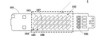
- FIG. 1 is one schematic view of the structure of the circuit board 1 of Example 1 of the present invention
- FIGS. 2A to 2C are examples of the present invention. It is another schematic diagram of the structure of the circuit board 1 of FIG.
- the circuit board 1 includes the following. Substrate 101; and a reinforcing device 102 provided on the substrate 101 (indicated by a dashed frame in FIGS. 1 and 2A to 2C).
- the reinforcing device 102 includes two or more lands 103, and the lands 103 are arranged in at least two rows to form a first row of lands 104 and a second row of lands 105. 2A to 2C, even if the lands 104 of the first row intersect with the lands 105 of the second row, as shown in FIG. 1, the lands 104 of the first row and the lands 105 of the second row And may be staggered.
- the substrate 101 is provided with an electronic element 106, and this embodiment does not limit the installation form and type of the electronic element 106.
- the first row lands 104 and the second row lands 105 of the reinforcement device 102 intersect with each other or are arranged in a staggered manner to strengthen the strength of the substrate 101.
- the curved deformation of the substrate 101 can be corrected, and the electronic device 106 on the substrate 101 can be prevented from being damaged in a subsequent assembly process.
- the reinforcing device including two or more lands can be provided on the substrate to reinforce the substrate using a plurality of lands having a small area. Therefore, the amount of heat required for soldering can be effectively retained when the land is formed, and the land can be easily formed on the substrate.
- the circuit board 1 may be any type of circuit board.
- it may be a circuit board used for a proximity sensor or a circuit board used for other electronic products, and the present invention is not specifically limited to this.
- the land 103 can be formed on the substrate 101 by the reflow method or the flow method.
- the present application is not limited to this, and the land 103 may be formed on the substrate 101 by another method.
- the number of row lands formed by arranging the lands 103 may be two rows, such as the two rows shown in FIGS. 2A to 2C, or may be the four rows shown in FIG. The number may be more than two columns.
- the number of lands included in one row of lands may be one, such as one land shown in FIGS. 2A to 2C, and may be seven or eight shown in FIG. As such, it may be a number greater than one.
- the lands 104 in the first row and the lands 105 in the second row are arranged alternately, and the lands 104 in the first row and the lands 105 in the second row are respectively arranged.
- a first gap 107 is formed between the lands 103 in the first row of lands 104 including two or more lands 103, and a second gap 108 is formed between the lands 103 in the second row of lands 105. They are formed and the first gap 107 and the second gap 108 are offset from each other.
- the strength of the substrate 101 can be significantly improved by offsetting the first gap 107 and the second gap 108 from each other.
- the lands 103 are arranged in four rows, and any two adjacent lands 103 can be the lands 104 in the first column and the lands 105 in the second column. ..
- the installation method of the lands 104 of the first row and the lands 105 of the second row will be described by taking the third row and the fourth row as an example. It can be understood that the number of rows of the lands 103 in the present embodiment is not limited to four rows shown in FIG. 1, and the lands 103 of the reinforcing device 102 may be arranged in two or more rows.
- the reinforcing device 102 includes two lands 103, and the two lands 103 are respectively the first row land 104 and the second row land 105.
- the lands 104 in the first row and the lands 105 in the second row intersect with each other.
- the land 104 of the first row and the land 105 of the second row may form an X shape as shown in FIG. 2A or a V shape as shown in FIGS. 2B and 2C.
- the number of the lands 103 that intersect with each other in the present embodiment is not limited to two as shown in FIGS. 2A to 2C, and more than two lands 103 may intersect with each other to form the reinforcing device 102. I can understand.
- the geometrical contours of the lands 103 may be the same and may have the same size. Thereby, the curved deformation of the substrate can be corrected uniformly and symmetrically.
- the two lands 103 in the reinforcing device 102 are quadrangles having the same size.
- FIG. 3 is another schematic view of the structure of the circuit board 1 according to the first embodiment of the present invention. As shown in FIG. 3, the plurality of lands 103 in the reinforcing device 102 are rectangles having the same size.
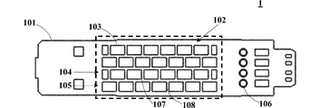
- FIG. 4 is another schematic view of the structure of the circuit board 1 according to the first embodiment of the present invention. As shown in FIG. 4, the plurality of lands 103 in the reinforcing device 102 are rectangles having the same size.
- the present application is not limited to this, and the geometrical contour of the land 103 or the size of the land may be different.
- the geometric outer shape of the land 103 may be a circle, a polygon, or a combination of both. As shown in FIGS. 1 to 4, the geometric outer shape of the land 103 is a quadrangle. However, the present application is not limited to this, and the geometric outer shape of the land 103 may be a polygon such as a triangle, a pentagon, or a hexagon, or may be a circle, and the geometric shape of a part of the land 103 may be used.
- the external shape may be polygonal, and the geometrical external shape of the other land 103 may be circular. As a result, the shape and position of the land 103 can be provided more flexibly.
- the included angle ⁇ between the long side of the land 103 and the long side of the substrate 101 is less than 45 degrees. Since the longer the substrate 101 is, the larger the bending deformation is, the bending deformation in the long side direction of the substrate 101 is larger than the bending deformation in the short side direction.
- the included angle ⁇ between the long side of the land 103 and the long side of the substrate 101 is less than 45 degrees, the projection of the long side of the land 103 onto the long side of the substrate 101 is the projection of the substrate 101 onto the short side. This makes it possible to increase the strength of the substrate 101 in the long side direction.
- the present application is not limited to this, and the included angle ⁇ between the long side of the rectangular land 103 and the long side of the substrate 101 may be 45 degrees or more.
- the long side of the rectangular land 103 and the long side of the substrate 101 are parallel to each other. Accordingly, the strength of the substrate 101 in the long side direction can be further increased, and the bending deformation of the substrate 101 in the long side direction can be further corrected.
- the included angle ⁇ between the long side of the land 103 and the long side of the substrate 101 is less than 45 degrees. Since the projection of the long side of the land 103 onto the long side of the substrate 101 is larger than the projection onto the short side of the substrate 101, the strength of the substrate 101 in the long side direction can be increased. However, the present application is not limited to this, and the included angle ⁇ between the long side of the rectangular land 103 and the long side of the substrate 101 may be 45 degrees or more.
- the reinforcing device 102 may be provided on either one side or both sides of the substrate 101. As shown in FIGS. 1 and 4, the reinforcing device 102 may be provided on one surface of the substrate 101. As shown in FIGS. 2A to 2C and FIG. 3, the reinforcing device 102 may be provided on the other surface of the substrate 101. Alternatively, the reinforcing device 102 may be provided on both surfaces of the substrate 101 at the same time, which can further increase the strength of the substrate 101.
- the land 103 may be provided at any position on the substrate 101 that does not interfere with the electronic element 106.
- the reinforcing device 102 may be provided centrally in the central position of the substrate 101, which can prevent the bending deformation from occurring in the central part of the substrate 101. ..
- the land 103 does not have to be connected to the wiring (not shown) on the substrate 101, which can reduce the manufacturing cost of the reinforcing device 102.
- the present application is not limited to this, and the land 103 may be connected to the wiring on the substrate 101.
- the pattern of the reinforcing device 102 provided on one surface of the substrate 101 and the reinforcing device 102 provided on the other surface of the substrate 101 may be symmetrical with respect to the substrate 101. Thereby, the curved deformation of the substrate 101 can be corrected uniformly and symmetrically.
- the pattern of the reinforcement device 102 refers to the number of lands 103 in the reinforcement device 102, the geometrical shape, the size, the arrangement method, the installation position, and the like.
- FIG. 5 is another schematic view of the structure of the circuit board 1 according to the first embodiment of the present invention.
- the reinforcing device 102 is provided on one surface of the substrate 101, and in FIG. 5, the reinforcing device 102 is provided on the other surface of the substrate 101, and the reinforcing device 102 is provided on the substrate 101.
- the pattern on one side (shown in FIG. 1) and the pattern on the other side of the substrate 101 (shown in FIG. 5) are symmetrical with respect to the substrate 101.
- the present application is not limited to this, and the pattern on one surface of the substrate 101 and the pattern on the other surface of the substrate 101 of the reinforcing device 102 may not be symmetrical with respect to the substrate 101.
- the reinforcing device is provided on the substrate, and the lands of the first row and the lands of the second row of the reinforcing device intersect with each other or are arranged in a staggered manner to strengthen the strength of the board.
- the curved deformation of the substrate can be corrected, and the electronic device on the substrate can be prevented from being damaged during the subsequent assembling process.
- the reinforcing device including two or more lands can be provided on the substrate to reinforce the substrate using a plurality of lands having a small area. Therefore, the amount of heat required for soldering can be effectively retained when the land is formed, and the land can be easily formed on the substrate.
- Example 2 of the present invention provides a proximity sensor including the circuit board described in Example 1 of the present invention.
- the reinforcing device is provided on the substrate of the circuit board 1, so that the lands of the first row and the lands of the second row of the reinforcing device are mutually arranged. It can be crossed or staggered to enhance the strength of the board, correct the curved deformation of the board, and avoid the damage of the electronic elements on the board during the subsequent assembly process. The reliability can be increased.
- the reinforcement device including two or more lands can be provided on the substrate to reinforce the substrate with a plurality of lands having a small area. Therefore, the amount of heat required for soldering can be effectively held when the land is formed, the land can be easily formed on the substrate, and the manufacturing cost of the proximity sensor can be reduced.
- the proximity sensor 2 is capable of detecting movement information and/or presence information of a target, converting the detected information into an electric signal and outputting the electric signal, and the capacitance type proximity sensor and the inductive type proximity sensor.
- the capacitance type proximity sensor and the inductive type proximity sensor any one of a photoelectric proximity sensor and the like may be used.
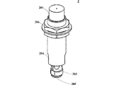
- FIG. 6 is a schematic diagram of the structure of the proximity sensor 2 according to the second embodiment of the present invention
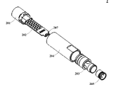
- FIG. 7 is an exploded schematic diagram of the proximity sensor 2 shown in FIG.
- the proximity sensor 2 may include a detection unit 201, a control unit 202, a display unit 203, an appearance protection unit 204, an output unit 205, and a fixed unit 206. ..
- the present application is not limited to this, and the proximity sensor 2 may include a member other than the above members, or may include only a part of the above members.
- the detection unit 201 may be a magnetic type detection unit including a coil housing or the like, and detects movement information and/or presence information of an object using an electromagnetic induction technology.
- the present application is not limited to this, and the detection unit 201 may be another type of detection unit.
- the control unit 202 may be provided with the circuit board 1 described in the first embodiment of the present invention.
- the control unit 202 is electrically connected to the detection unit 201 and the output unit 205 and controls the operations of the detection unit 201 and the output unit 205.
- a light emitting diode 207 may be provided on the circuit board 1 of the control unit 202, and information such as whether or not an electric signal is output is displayed by the color of the LED 207, the blinking method, or the like.
- the display unit 203 may be arranged so as to face the LED 207 on the circuit board 1 of the control unit 202, and the light of the LED 207 can pass through the display unit 203 and be captured outside.
- the display 203 may be in the form of a light emitting hole, for example.
- the present application is not limited to this, and the display unit 203 may be another type of display unit.
- the appearance protection unit 204 may have a cylindrical shape that covers the control unit 202, the detection unit 201 is exposed from one end of the appearance protection unit 204, and the display unit 203 is exposed from the other end of the appearance protection unit 204.
- the present application is not limited to this, and the appearance protection unit 204 may be a member having another shape.
- the output unit 205 may be electrically connected to the control unit 202 and is used to output an electric signal to the outside.
- the fixing unit 206 is used to fix the proximity sensor to the client and can be attached to the outer peripheral portion of the appearance protecting unit 204.
- the reinforcing device is provided on the board of the circuit board, so that the land of the first row and the second row of the reinforcing device are provided.
- the lands may be crossed with each other or staggered to enhance the strength of the substrate, correct the curved deformation of the substrate, and prevent the electronic devices on the substrate from being damaged in the subsequent assembly process, The reliability of the proximity sensor can be improved.
- the reinforcing device including two or more lands can be provided on the substrate to reinforce the substrate using a plurality of lands having a small area. Therefore, the amount of heat required for soldering can be effectively held when the land is formed, the land can be easily formed on the substrate, and the manufacturing cost of the proximity sensor can be reduced.
Landscapes
- Engineering & Computer Science (AREA)
- Microelectronics & Electronic Packaging (AREA)
- Manufacturing & Machinery (AREA)
- Structure Of Printed Boards (AREA)
Abstract
本発明の実施例は、回路基板及びこの回路基板を含む近接センサを提供する。この回路基板は、基板と、基板上に設けられた補強装置と、を含み、この補強装置は、2個以上のランドを含み、このランドは、少なくとも2列に配列されることで、第1列のランド及び第2列のランドを形成し、この第1列のランドとこの第2列のランドとは、互いに交差しているか、又は、この第1列のランドとこの第2列のランドは、互い違いに配列されている。本発明は、上記補強装置を設けることにより、基板の強度を強化し、基板の湾曲変形を矯正することができ、且つ基板上に補強装置を容易に形成することができる。
Description
本発明は、基板技術分野に関し、特に回路基板及びこの回路基板を含む近接センサに関する。
近年、産業機器の高性能化に伴い、基板及び基板上に搭載された部品の精度が高まっている。
上記技術的背景の紹介は、本発明の技術手法について明瞭、完全な説明を行い、当業者の理解に便利なように説明するためのものに過ぎないことに注意すべきである。これらの手法が本発明の背景技術の一部しか説明していないことを理由に、上記技術手法が当業者にとって公知のものであるとすることはできない。
通常、基板の加工作成後に1%から2%の湾曲変形が存在し、基板に対して後続する組み立てを行う過程で、外部から加えられる、基板の湾曲変形方向とは逆の応力を基板が受ける。基板上の電子素子は、基板に湾曲変形が存在する状況の下で基板上に実装されるため、外部からの上記応力を基板が受けたときに、基板上の電子素子が破損しやすく、経済的損失がもたらされる。
上記課題を解決するため、本発明の実施例は、補強装置によって基板の強度を強化し、基板の湾曲変形を矯正することができ、且つ基板上にこの補強装置を容易に形成することができる回路基板及びこの回路基板を含む近接センサを提供する。
本発明の実施例の第1の態様は、基板と、前記基板上に設けられ、2個以上のランドを含む補強装置と、を備え、前記ランドは、少なくとも2列に配列されることで、第1列のランド及び第2列のランドを形成し、前記第1列のランドと前記第2列のランドとが互いに交差しているように配置されており、又は、前記第1列のランドと前記第2列のランドとが互い違いに配列されていることを特徴とする回路基板を提供する。
本発明の実施例の第2の態様は、前記第1列のランドと前記第2列のランドが互い違いに配列している場合、前記第1列のランド及び前記第2列のランドは、それぞれ2個以上のランドを含み、前記第1列のランドにおけるランド間に第1の間隙が形成され、前記第2列のランドにおけるランド間に第2の間隙が形成され、前記第1の間隙と前記第2の間隙とが互いにずれている、第1の態様に記載の回路基板を提供する。
本発明の実施例の第3の態様は、前記ランドの幾何学的外形が同一であり、大きさが一致している、第1の態様に記載の回路基板を提供する。
本発明の実施例の第4の態様は、前記ランドの幾何学的外形が円形、多角形又は両者の組み合わせである、第1の態様に記載の回路基板を提供する。
本発明の実施例の第5の態様は、前記第1列のランドと前記第2列のランドとが互い違いに配列しており、且つ前記ランドの幾何学的外形が四角形である場合、前記四角形のランドの長辺と前記基板の長辺との間の夾角が45度未満である、第1の態様に記載の回路基板を提供する。
本発明の実施例の第6の態様は、前記四角形のランドの長辺と前記基板の長辺とが平行である、第5の態様に記載の回路基板を提供する。
本発明の実施例の第7の態様は、前記第1列のランドと前記第2列のランドとが互いに交差しており、且つ前記ランドの幾何学的外形が四角形である場合、前記四角形のランドの長辺と前記基板の長辺との間の夾角が45度未満である、第1の態様に記載の回路基板を提供する。
本発明の実施例の第8の態様は、前記補強装置が、前記基板のいずれか一方の面又は両面に設けられている、第1の態様に記載の回路基板を提供する。
本発明の実施例の第9の態様は、前記補強装置が前記基板の両面に設けられている場合、前記基板の一方の面に設けられた前記補強装置のパターンと前記基板の他方の面に設けられた前記補強装置のパターンとが、前記基板に対して対称である、第8の態様に記載の回路基板を提供する。
本発明の実施例の第10の態様は、前記第1列のランドと前記第2列のランドとが互いに交差している場合、前記第1列のランド及び前記第2列のランドがX字形又はV字形を形成する、第1の態様に記載の回路基板を提供する。
本発明の実施例の第11の態様は、第1の態様から第10の態様のいずれかに記載の回路基板を含む、近接センサを提供する。
本発明の実施例の有益な効果は、以下のとおりである。基板上に補強装置を設けることにより、補強装置の第1列のランドと第2列のランドとが互いに交差するか、又は互い違いに配列され、これによって、基板の強度を強化し、基板の湾曲変形を矯正することができ、後続する組み立て過程において、基板上の電子素子が破損することを回避することができる。それとともに、1つの連続したランドを基板上に形成する補強方式と比べ、2個以上のランドを含む補強装置を基板上に設けることにより、面積が小さい複数のランドを用いて基板を補強することができるため、ランド形成時に、はんだ付けに必要な熱量を有効に保持することができ、基板上にランドを容易に形成することができる。
以下の説明及び図面を参照し、本発明の特定の実施形態を詳細に開示し、本発明の原理で採用可能な態様を明示する。本発明の実施形態は、範囲上、これによって限定されるものではないと理解すべきである。請求の範囲の趣旨及び条項の範囲内で、本発明の実施形態は、多くの変更、修正及び均等物を含む。
実施形態の記述及び/又は示された特徴は、同一又は類似の態様で、1つ又は複数のその他の実施形態において用いることができ、その他の実施形態における特徴と組み合わせるか、又はその他の実施形態における特徴の代わりとすることができる。
なお、「備える/含む」という用語を本文において使用する際には、特徴、部材、ステップ又はアセンブリの存在をいうが、1つ又は複数のその他の特徴、部材、ステップ又はアセンブリの存在又は付加を排除しない。
図面の説明
含まれる図面は、本発明の実施例に対するさらなる理解のために提供されるものであり、明細書の一部を構成し、本発明の実施形態を例示し、文字の記述とともに本発明の原理を説明するために用いられるものである。次の記述における図面は、本発明の実施例の一部であるに過ぎず、当業者にとって、創造的な労働を行わない前提の下で、これらの図面に基づきその他の図面をさらに得ることができることは自明のことである。
含まれる図面は、本発明の実施例に対するさらなる理解のために提供されるものであり、明細書の一部を構成し、本発明の実施形態を例示し、文字の記述とともに本発明の原理を説明するために用いられるものである。次の記述における図面は、本発明の実施例の一部であるに過ぎず、当業者にとって、創造的な労働を行わない前提の下で、これらの図面に基づきその他の図面をさらに得ることができることは自明のことである。
具体的な実施形態
図面を参照し、以下の明細書によって、本発明の前述の及びその他の特徴が明確になる。明細書及び図面において、本発明の特定の実施形態を具体的に開示しており、本発明の原理を採用可能な一部の実施形態を表している。なお、本発明は、記述された実施形態に限定されるものではなく、逆に、本発明は、請求の範囲に入るすべての修正、変更及び均等物を含む。
図面を参照し、以下の明細書によって、本発明の前述の及びその他の特徴が明確になる。明細書及び図面において、本発明の特定の実施形態を具体的に開示しており、本発明の原理を採用可能な一部の実施形態を表している。なお、本発明は、記述された実施形態に限定されるものではなく、逆に、本発明は、請求の範囲に入るすべての修正、変更及び均等物を含む。
本発明の実施例において、単数形である「1つの」、「この」などは、複数形を含み、「1種の」又は「類の」と理解すべきであり、「1個」の意味であると限定するものではない。また、上下の文で別途明確に指摘している場合を除き、「前記」という用語は、単数形だけでなく、複数形も含むと理解すべきである。また、上下の文で別途明確に指摘している場合を除き、「による」という用語は、「少なくとも一部が・・・・・・による」と理解すべきであり、「に基づく」という用語は、「少なくとも一部が・・・・・・に基づく」と理解すべきである。
実施例1
本発明の実施例1は、回路基板を提供し、図1は、本発明の実施例1の回路基板1の構造の1つの模式図であり、図2Aから図2Cは、本発明の実施例1の回路基板1の構造の他の模式図である。
本発明の実施例1は、回路基板を提供し、図1は、本発明の実施例1の回路基板1の構造の1つの模式図であり、図2Aから図2Cは、本発明の実施例1の回路基板1の構造の他の模式図である。
本実施例において、図1及び図2Aから図2Cに示すように、回路基板1は、次のものを含む。
基板101;及び
基板101上に設けられた補強装置102(図1及び図2Aから図2Cにおいて破線の枠で示す)。補強装置102は、2個以上のランド103を含み、ランド103は、少なくとも2列に配列されて第1列のランド104及び第2列のランド105を形成する。図2Aから図2Cに示すように、第1列のランド104が第2列のランド105と互いに交差しても、図1に示すように、第1列のランド104と第2列のランド105とが互い違いに配列してもよい。
基板101;及び
基板101上に設けられた補強装置102(図1及び図2Aから図2Cにおいて破線の枠で示す)。補強装置102は、2個以上のランド103を含み、ランド103は、少なくとも2列に配列されて第1列のランド104及び第2列のランド105を形成する。図2Aから図2Cに示すように、第1列のランド104が第2列のランド105と互いに交差しても、図1に示すように、第1列のランド104と第2列のランド105とが互い違いに配列してもよい。
また、図1及び図2Aから図2Cに示すように、上記基板101には、電子素子106が設けられており、本実施例は、この電子素子106の設置形式及び種類を限定しない。
基板101上に補強装置102を設けることにより、補強装置102の第1列のランド104と第2列のランド105とが互いに交差するか、又は互い違いに配列され、基板101の強度を強化し、基板101の湾曲変形を矯正することができ、後続する組み立て過程において、基板101上の電子素子106が破損することを回避することができる。且つ、1つの連続したランドを基板上に形成する補強方式と比べ、2個以上のランドを含む補強装置を基板上に設けることにより、面積が小さい複数のランドを用いて基板を補強することができるため、ランド形成時に、はんだ付けに必要な熱量を有効に保持することができ、基板上にランドを容易に形成することができる。
本実施例において、回路基板1は、いかなるタイプの回路基板であってもよい。例えば、近接センサに用いられる回路基板であってもよく、その他の電子製品に用いられる回路基板であってもよく、本発明はこれについて具体的に限定しない。
本実施例において、リフロー方式又はフロー方式で基板101上にランド103を形成することができる。しかしながら、本願はこれに限定されず、その他の方式で基板101上にランド103を形成してもよい。
本実施例において、ランド103を配列して形成される列ランドの数は、図2Aから図2Cに示す2列のように、2列であってもよく、図1に示す4列のように、2列を超える数であってもよい。
本実施例において、1列のランドに含まれるランドの数は、図2Aから図2Cに示す1個のランドのように、1個であってもよく、図1に示す7個又は8個のように、1を超える数であってもよい。
本実施例において、図1に示すように、第1列のランド104と第2列のランド105は、互い違いに配列しており、第1列のランド104及び第2列のランド105は、それぞれ2個以上のランド103を含み、第1列のランド104におけるランド103の間に第1の間隙107が形成されており、第2列のランド105におけるランド103の間に第2の間隙108が形成されており、第1の間隙107と第2の間隙108とは互いにずれている。第1の間隙107と第2の間隙108とを揃える設置方式に比べ、第1の間隙107と第2の間隙108とを互いにずらすことにより、基板101の強度を著しく向上させることができる。
本実施例において、図1に示すように、ランド103を4行に配列し、隣接するいずれの2列のランド103も、第1列のランド104及び第2列のランド105とすることができる。例えば、図1において、第3列及び第4列を例に、第1列のランド104及び第2列のランド105の設置方式について説明する。本実施例におけるランド103の列数は、図1に示す4列に限定されず、補強装置102のランド103を2列以上に配列すればよいと理解することができる。
本実施例において、図2Aから図2Cに示すように、補強装置102は、2個のランド103を含み、この2個のランド103は、それぞれ第1列のランド104及び第2列のランド105とすることができ、この第1列のランド104及び第2列のランド105は互いに交差する。例えば、この第1列のランド104及び第2列のランド105は、図2Aに示すようにX字形を形成しても、図2B及び図2Cに示すようにV字形を形成してもよい。本実施例における互いに交差したランド103の個数は、図2Aから図2Cに示すように2個に限定されず、2個を超えるランド103を互いに交差させて補強装置102を形成してもよいと理解することができる。
本実施例において、ランド103の幾何学的外形は、同一であり、且つ大きさが一致していてもよい。これにより、基板の湾曲変形を均等且つ対称に矯正することができる。図2Aから図2Cに示すように、補強装置102における2個のランド103は、大きさが同一な四角形である。図3は、本発明の実施例1の回路基板1の構造の他の模式図である。図3に示すように、補強装置102における複数のランド103は、大きさが同一な矩形である。図4は、本発明の実施例1の回路基板1の構造の他の模式図である。図4に示すように、補強装置102における複数のランド103は、大きさが同一な矩形である。しかしながら、本願はこれに限定されず、ランド103の幾何学的外形又はランドの大きさは異なっていてもよい。
本実施例において、ランド103の幾何学的外形は、円形、多角形又は両者の組み合わせであってもよい。図1から図4に示すように、ランド103の幾何学的外形は、四角形である。しかしながら、本願はこれに限定されず、ランド103の幾何学的外形は、三角形、五角形、六角形などの多角形であってもよく、円形であってもよく、一部のランド103の幾何学的外形が多角形であり、他の部分のランド103の幾何学的外形が円形であってもよい。これにより、ランド103の形状及び位置をより柔軟に設けることができる。
本実施例において、図3に示すように、第1列のランド104と第2列のランド105とが互い違いに配列しており、且つランド103の幾何学的外形が四角形である場合、四角形のランド103の長辺と基板101の長辺との間の夾角αは45度未満である。基板101が長いほど湾曲変形が大きくなるため、基板101の長辺方向の湾曲変形は、短辺方向の湾曲変形よりも大きい。ランド103の長辺と基板101の長辺との間の夾角αを45度未満にすることにより、基板101の長辺へのランド103の長辺の投影が、短辺への基板101の投影よりも大きくなり、これにより、長辺方向における基板101の強度を高めることができる。しかしながら、本願はこれに限定されず、四角形のランド103の長辺と基板101の長辺との間の夾角αは、45度以上であってもよい。
本実施例において、図1及び図4に示すように、四角形のランド103の長辺と基板101の長辺とは平行である。これにより、長辺方向における基板101の強度をさらに高めることができ、長辺方向における基板101の湾曲変形をさらに矯正することができる。
本実施例において、図2Aから図2Cに示すように、第1列のランド104及び第2列のランド105が互いに交差しており、且つランド103の幾何学的外形が四角形である場合、四角形のランド103の長辺と基板101の長辺との間の夾角θは45度未満である。基板101の長辺へのランド103の長辺の投影が基板101の短辺への投影よりも大きいため、長辺方向における基板101の強度を高めることができる。しかしながら、本願はこれに限定されず、四角形のランド103の長辺と基板101の長辺との間の夾角θは、45度以上であってもよい。
本実施例において、補強装置102は、基板101のいずれか一方の面に設けても両面に設けてもよい。図1、図4に示すように、補強装置102は、基板101の一方の面に設けてもよい。図2Aから図2C及び図3に示すように、補強装置102は、基板101の他方の面に設けてもよい。又は、補強装置102は、基板101の両面に同時に設けてもよく、これにより、基板101の強度をさらに高めることができる。
本実施例において、ランド103は、基板101上の電子素子106に対して干渉を生じないいずれの位置に設けてもよい。例えば、図1から図4に示すように、補強装置102は、基板101の中央位置に集中して設けてもよく、これにより、基板101の中央から湾曲変形が生じることを防止することができる。
本実施例において、ランド103は、基板101上の配線(図示せず)と接続しなくてもよく、これにより、補強装置102の製造コストを下げることができる。しかしながら、本願はこれに限定されず、ランド103は、基板101上の配線と接続してもよい。
本実施例において、補強装置102が基板101の両面に設けられている場合、基板101の一方の面に設けられた補強装置102のパターンと基板101の他方の面に設けられた補強装置102のパターンとが、基板101に対して対称であってもよい。これにより、基板101の湾曲変形を均等且つ対称に矯正することができる。
ここで、補強装置102のパターンとは、補強装置102におけるランド103の数、幾何学的形状、大きさ、配列方式及び設置位置などをいう。図5は、本発明の実施例1の回路基板1の構造の他の模式図である。図1において、補強装置102は、基板101の一方の面に設けられており、図5において、補強装置102は、基板101の他方の面に設けられており、補強装置102は、基板101の一方の面におけるパターン(図1に示す)と基板101の他方の面におけるパターン(図5に示す)とが、基板101に対して対称である。しかしながら、本願はこれに限定されず、補強装置102の基板101の一方の面におけるパターンと基板101の他方の面におけるパターンとは、基板101に対して対称でなくてもよい。
本実施例の回路基板によって、基板上に補強装置を設け、補強装置の第1列のランドと第2列のランドとが互いに交差するか、又は互い違いに配列され、基板の強度を強化し、基板の湾曲変形を矯正することができ、後続する組み立て過程において、基板上の電子素子が破損することを回避することができる。且つ、1つの連続したランドを基板上に形成する補強方式と比べ、2個以上のランドを含む補強装置を基板上に設けることにより、面積が小さい複数のランドを用いて基板を補強することができるため、ランド形成時に、はんだ付けに必要な熱量を有効に保持することができ、基板上にランドを容易に形成することができる。
実施例2
本発明の実施例2は、本発明の実施例1に記載の回路基板を含む近接センサを提供する。本発明の実施例1に記載の回路基板1を近接センサに設けることによって、回路基板1の基板上に補強装置を設けることにより、補強装置の第1列のランドと第2列のランドを互いに交差させるか、又は互い違いに配列し、基板の強度を強化し、基板の湾曲変形を矯正し、後続する組み立て過程において、基板上の電子素子が破損することを回避することができ、近接センサの信頼性を高めることができる。且つ、1つの連続したランドを基板上に形成する補強方式と比べ、2個以上のランドを含む補強装置を基板上に設けることにより、面積が小さい複数のランドを用いて基板を補強することができるため、ランド形成時に、はんだ付けに必要な熱量を有効に保持することができ、基板上にランドを容易に形成し、近接センサの製造コストを下げることができる。
本発明の実施例2は、本発明の実施例1に記載の回路基板を含む近接センサを提供する。本発明の実施例1に記載の回路基板1を近接センサに設けることによって、回路基板1の基板上に補強装置を設けることにより、補強装置の第1列のランドと第2列のランドを互いに交差させるか、又は互い違いに配列し、基板の強度を強化し、基板の湾曲変形を矯正し、後続する組み立て過程において、基板上の電子素子が破損することを回避することができ、近接センサの信頼性を高めることができる。且つ、1つの連続したランドを基板上に形成する補強方式と比べ、2個以上のランドを含む補強装置を基板上に設けることにより、面積が小さい複数のランドを用いて基板を補強することができるため、ランド形成時に、はんだ付けに必要な熱量を有効に保持することができ、基板上にランドを容易に形成し、近接センサの製造コストを下げることができる。
本実施例において、近接センサ2は、対象の移動情報及び/又は存在情報を検出し、検出した情報を電気信号に変換して出力することができ、静電容量形近接センサ、誘導形近接センサ又は光電形近接センサなどのうちのいずれか1種であってもよい。
図6は、本発明の実施例2の近接センサ2の構造の模式図であり、図7は、図6に示す近接センサ2の分解模式図である。図6及び図7に示すように、近接センサ2は、検出部201と、制御部202と、表示部203と、外観保護部204と、出力部205と、固定部206と、を含んでもよい。しかしながら、本願はこれに限定されず、近接センサ2は、以上の部材以外の他の部材を含んでも、以上の部材のうちの一部の部材のみを含んでもよい。
検出部201は、コイル筐体などからなる磁気型検出部であってもよく、電磁誘導技術を用いて対象物の移動情報及び/又は存在情報を検出する。しかしながら、本願はこれに限定されず、検出部201は、他のタイプの検出部であってもよい。
制御部202において、本発明の実施例1に記載の回路基板1が設けられていてもよい。制御部202は、検出部201及び出力部205と電気的に接続し、検出部201及び出力部205の動作を制御する。制御部202の回路基板1上には、発光ダイオード207(LED)が設けられていてもよく、LED 207の色、点滅方式などによって、電気信号の出力があるかどうかなどの情報を表示する。
表示部203は、制御部202の回路基板1上のLED 207と対向して配置してもよく、LED 207の光は、表示部203を通過して外部で捉えることができる。表示部203は、例えば、発光穴の形式であってもよい。しかしながら、本願はこれに限定されず、表示部203は、他のタイプの表示部であってもよい。
外観保護部204は、制御部202を覆う円筒状であってもよく、検出部201は、外観保護部204の一端から露出し、表示部203は、外観保護部204の他端から露出する。しかしながら、本願はこれに限定されず、外観保護部204は、他の形状の部材であってもよい。
出力部205は、制御部202と電気的に接続していてもよく、外に電気信号を出力するために用いられる。
固定部206は、近接センサをクライアントに固定するために用いられ、外観保護部204の外周部に取り付けることができる。
本実施例において、本発明の実施例1に記載の回路基板を近接センサに設けることによって、回路基板の基板上に補強装置を設けることにより、補強装置の第1列のランドと第2列のランドを互いに交差させるか、又は互い違いに配列し、基板の強度を強化し、基板の湾曲変形を矯正し、後続する組み立て過程において、基板上の電子素子が破損することを回避することができ、近接センサの信頼性を高めることができる。且つ、1つの連続したランドを基板上に形成する補強方式と比べ、2個以上のランドを含む補強装置を基板上に設けることにより、面積が小さい複数のランドを用いて基板を補強することができるため、ランド形成時に、はんだ付けに必要な熱量を有効に保持することができ、基板上にランドを容易に形成し、近接センサの製造コストを下げることができる。
以上、具体的な実施形態を合わせて本発明について記述したが、当業者は、これらの記述は例示的なものであり、本発明の保護範囲に対する限定ではないことを明確にすべきである。当業者は、本発明の趣旨及び原理により本発明に対して各種変更及び修正を行うことができ、これらの変更及び修正も本発明の範囲内にある。
Claims (11)
- 基板と、
前記基板上に設けられ、2個以上のランドを含む補強装置と、を備え、
前記ランドは、少なくとも2列に配列されることで、第1列のランド及び第2列のランドを形成し、前記第1列のランドと前記第2列のランドとが互いに交差しているように配置されており、又は、前記第1列のランドと前記第2列のランドとが互い違いに配列されていることを特徴とする回路基板。 - 前記第1列のランドと前記第2列のランドとが互い違いに配列している場合、前記第1列のランド及び前記第2列のランドは、それぞれ2個以上のランドを含み、前記第1列のランドにおけるランド間に第1の間隙が形成され、前記第2列のランドにおけるランド間に第2の間隙が形成され、前記第1の間隙と前記第2の間隙とが互いにずれていることを特徴とする請求項1に記載の回路基板。
- 前記ランドの幾何学的外形が同一であり、大きさが一致していることを特徴とする請求項1に記載の回路基板。
- 前記ランドの幾何学的外形が円形、多角形又は両者の組み合わせであることを特徴とする請求項1に記載の回路基板。
- 前記第1列のランドと前記第2列のランドとが互い違いに配列しており、且つ前記ランドの幾何学的外形が四角形である場合、前記四角形のランドの長辺と前記基板の長辺との間の夾角が45度未満であることを特徴とする請求項1に記載の回路基板。
- 前記四角形のランドの長辺と前記基板の長辺とが平行であることを特徴とする請求項5に記載の回路基板。
- 前記第1列のランドと前記第2列のランドとが互いに交差しており、且つ前記ランドの幾何学的外形が四角形である場合、前記四角形のランドの長辺と前記基板の長辺との間の夾角が45度未満であることを特徴とする請求項1に記載の回路基板。
- 前記補強装置が、前記基板のいずれか一方の面又は両面に設けられていることを特徴とする請求項1に記載の回路基板。
- 前記補強装置が前記基板の両面に設けられている場合、前記基板の一方の面に設けられた前記補強装置のパターンと前記基板の他方の面に設けられた前記補強装置のパターンとが、前記基板に対して対称であることを特徴とする請求項8に記載の回路基板。
- 前記第1列のランドと前記第2列のランドとが互いに交差している場合、前記第1列のランド及び前記第2列のランドがX字形又はV字形を形成することを特徴とする請求項1に記載の回路基板。
- 請求項1~10のいずれか一項に記載の回路基板を含むことを特徴とする近接センサ。
Applications Claiming Priority (2)
| Application Number | Priority Date | Filing Date | Title |
|---|---|---|---|
| CN201920053504.8U CN209643079U (zh) | 2019-01-11 | 2019-01-11 | 电路基板以及包含该电路基板的接近传感器 |
| CN201920053504.8 | 2019-01-11 |
Publications (1)
| Publication Number | Publication Date |
|---|---|
| WO2020145349A1 true WO2020145349A1 (ja) | 2020-07-16 |
Family
ID=68477615
Family Applications (1)
| Application Number | Title | Priority Date | Filing Date |
|---|---|---|---|
| PCT/JP2020/000479 Ceased WO2020145349A1 (ja) | 2019-01-11 | 2020-01-09 | 回路基板及びこの回路基板を含む近接センサ |
Country Status (2)
| Country | Link |
|---|---|
| CN (1) | CN209643079U (ja) |
| WO (1) | WO2020145349A1 (ja) |
Families Citing this family (1)
| Publication number | Priority date | Publication date | Assignee | Title |
|---|---|---|---|---|
| CN111479383A (zh) * | 2020-05-15 | 2020-07-31 | 武汉华星光电技术有限公司 | 柔性印制电路板及显示面板 |
Citations (4)
| Publication number | Priority date | Publication date | Assignee | Title |
|---|---|---|---|---|
| JPH06326426A (ja) * | 1993-05-13 | 1994-11-25 | Sony Corp | フレキシブル配線基板 |
| JPH08235985A (ja) * | 1995-02-22 | 1996-09-13 | Omron Corp | 電子センサ |
| JP2003168848A (ja) * | 2001-11-30 | 2003-06-13 | Nec Kansai Ltd | 配線基板 |
| JP2007128959A (ja) * | 2005-11-01 | 2007-05-24 | Toshiba Corp | 半導体メモリカードおよび回路基板 |
-
2019
- 2019-01-11 CN CN201920053504.8U patent/CN209643079U/zh active Active
-
2020
- 2020-01-09 WO PCT/JP2020/000479 patent/WO2020145349A1/ja not_active Ceased
Patent Citations (4)
| Publication number | Priority date | Publication date | Assignee | Title |
|---|---|---|---|---|
| JPH06326426A (ja) * | 1993-05-13 | 1994-11-25 | Sony Corp | フレキシブル配線基板 |
| JPH08235985A (ja) * | 1995-02-22 | 1996-09-13 | Omron Corp | 電子センサ |
| JP2003168848A (ja) * | 2001-11-30 | 2003-06-13 | Nec Kansai Ltd | 配線基板 |
| JP2007128959A (ja) * | 2005-11-01 | 2007-05-24 | Toshiba Corp | 半導体メモリカードおよび回路基板 |
Also Published As
| Publication number | Publication date |
|---|---|
| CN209643079U (zh) | 2019-11-15 |
Similar Documents
| Publication | Publication Date | Title |
|---|---|---|
| US20190053406A1 (en) | Semiconductor device | |
| JP6186058B2 (ja) | 電子デバイスおよびその単層相互静電容量方式タッチスクリーン | |
| EP3844548A1 (en) | Micromirror actuator assembly | |
| US20200146157A1 (en) | Method of Enhancing Fatigue Life of Grid Arrays | |
| WO2010070964A1 (ja) | 回路モジュール及びその管理方法 | |
| US20190115285A1 (en) | Lead structure of circuit | |
| CN209643079U (zh) | 电路基板以及包含该电路基板的接近传感器 | |
| JP2001119107A (ja) | プリント配線板 | |
| US20200104012A1 (en) | Touch display panel, method of manufacturing touch display panel, and display apparatus | |
| CN107562249A (zh) | 触控显示装置 | |
| CN104461094B (zh) | 触控显示器 | |
| KR101065279B1 (ko) | 신호전송라인에 형성되는 슬롯 패턴을 구비하는인쇄회로기판 | |
| KR102281769B1 (ko) | 터치입력장치 | |
| US20150108029A1 (en) | Apparatus for receiving substrate | |
| JP5560087B2 (ja) | 変形防止機構を備えた回路基板 | |
| KR20160122955A (ko) | 박막형 자기발생 코일 시스템 | |
| JP5741453B2 (ja) | プレスフィットピン | |
| CN216650094U (zh) | 电路板、功能组件及电子设备 | |
| JP2017022187A (ja) | 面実装電子部品 | |
| KR20140029679A (ko) | 연성인쇄회로기판 | |
| US8466376B2 (en) | Enclosure of electronic device | |
| US12483242B2 (en) | Coil system for an inductive proximity switch for flush or non-flush installation in a housing | |
| US20080266826A1 (en) | Assemblable substrate for in-line package and assembly with same | |
| US8159827B2 (en) | Circuit board and method of mounting electronic component on printed board | |
| KR100798778B1 (ko) | 인쇄회로기판 |
Legal Events
| Date | Code | Title | Description |
|---|---|---|---|
| 121 | Ep: the epo has been informed by wipo that ep was designated in this application |
Ref document number: 20738802 Country of ref document: EP Kind code of ref document: A1 |
|
| NENP | Non-entry into the national phase |
Ref country code: DE |
|
| 122 | Ep: pct application non-entry in european phase |
Ref document number: 20738802 Country of ref document: EP Kind code of ref document: A1 |
|
| NENP | Non-entry into the national phase |
Ref country code: JP |