WO2020145236A1 - 電磁波送信装置及び電磁波通信システム - Google Patents
電磁波送信装置及び電磁波通信システム Download PDFInfo
- Publication number
- WO2020145236A1 WO2020145236A1 PCT/JP2020/000049 JP2020000049W WO2020145236A1 WO 2020145236 A1 WO2020145236 A1 WO 2020145236A1 JP 2020000049 W JP2020000049 W JP 2020000049W WO 2020145236 A1 WO2020145236 A1 WO 2020145236A1
- Authority
- WO
- WIPO (PCT)
- Prior art keywords
- voltage
- voltage value
- signal
- electromagnetic wave
- value
- Prior art date
- Legal status (The legal status is an assumption and is not a legal conclusion. Google has not performed a legal analysis and makes no representation as to the accuracy of the status listed.)
- Ceased
Links
Images


Classifications
-
- H—ELECTRICITY
- H03—ELECTRONIC CIRCUITRY
- H03B—GENERATION OF OSCILLATIONS, DIRECTLY OR BY FREQUENCY-CHANGING, BY CIRCUITS EMPLOYING ACTIVE ELEMENTS WHICH OPERATE IN A NON-SWITCHING MANNER; GENERATION OF NOISE BY SUCH CIRCUITS
- H03B7/00—Generation of oscillations using active element having a negative resistance between two of its electrodes
- H03B7/02—Generation of oscillations using active element having a negative resistance between two of its electrodes with frequency-determining element comprising lumped inductance and capacitance
- H03B7/06—Generation of oscillations using active element having a negative resistance between two of its electrodes with frequency-determining element comprising lumped inductance and capacitance active element being semiconductor device
- H03B7/08—Generation of oscillations using active element having a negative resistance between two of its electrodes with frequency-determining element comprising lumped inductance and capacitance active element being semiconductor device being a tunnel diode
-
- H—ELECTRICITY
- H04—ELECTRIC COMMUNICATION TECHNIQUE
- H04B—TRANSMISSION
- H04B1/00—Details of transmission systems, not covered by a single one of groups H04B3/00 - H04B13/00; Details of transmission systems not characterised by the medium used for transmission
- H04B1/02—Transmitters
- H04B1/04—Circuits
-
- H—ELECTRICITY
- H04—ELECTRIC COMMUNICATION TECHNIQUE
- H04L—TRANSMISSION OF DIGITAL INFORMATION, e.g. TELEGRAPHIC COMMUNICATION
- H04L27/00—Modulated-carrier systems
- H04L27/02—Amplitude-modulated carrier systems, e.g. using on-off keying; Single sideband or vestigial sideband modulation
- H04L27/04—Modulator circuits; Transmitter circuits
Definitions
- the present invention relates to an electromagnetic wave transmission device and an electromagnetic wave communication system.
- An amplitude shift keying method (Amplitude-Shift keying modulation method, hereinafter referred to as ASK modulation method) is known as a communication modulation method used for an oscillation element for transmitting electromagnetic waves.
- An on-off modulation method (On Off keying modulation method, hereinafter referred to as OOK modulation method) is also known as one method included in the ASK modulation method as a communication modulation method.
- Patent Document 1 discloses a technique relating to an ASK modulation method in which a resonant tunneling diode (Resonant Tunneling Diode, hereinafter referred to as RTD) is used as an oscillation element for electromagnetic wave transmission.
- the technique is a technique that represents binary by switching between data in the oscillation region of the RTD (for example, a signal corresponding to On) and data in the non-oscillation region (for example, a signal corresponding to Off), that is, It is said that the technique represents On and Off by the difference in amplitude.
- Patent Document 2 discloses a technique relating to an ASK modulation method using a continuous oscillation terahertz wave such as RTD. Specifically, the technique is considered to be a technique in which variable light whose intensity is variable is superposed on a modulation element as signal light and the amplitude of a terahertz wave is modulated according to the signal intensity.
- Patent Document 1 and Patent Document 2 represent two values due to the difference in amplitude, there is a limitation in increasing the transmission speed (or communication speed).
- One of the problems to be solved by the present invention is to increase the transmission speed.
- the invention according to claim 1 is A transmitter that has a voltage-current characteristic that has a maximum value and a minimum value that is located on a higher voltage side than the maximum value, and that transmits an electromagnetic wave indicating a modulation signal;
- An acquisition unit that acquires a digital signal, A first voltage value of two levels or more of a first voltage region in which the digital signal is a voltage region of the maximum value voltage or more and the minimum value voltage or less, and a voltage region of less than the maximum value voltage.
- a modulator that modulates to It is an electromagnetic wave transmission device provided with.
- FIG. 1 is a schematic diagram of an electromagnetic wave communication system 10 of this embodiment.
- the electromagnetic wave communication system 10 includes an electromagnetic wave transmitting device 20 and an electromagnetic wave receiving device 30.
- the electromagnetic wave communication system 10 has a function of receiving the electromagnetic wave W transmitted by the electromagnetic wave transmission device 20 by the electromagnetic wave reception device 30.
- the electromagnetic wave W of this embodiment is an electromagnetic wave indicating a modulated signal described later.
- the electromagnetic wave W of this embodiment is, for example, a terahertz wave.
- the terahertz wave is said to be an electromagnetic wave having a shorter wavelength than a millimeter wave and a longer wavelength than infrared.
- Terahertz waves are electromagnetic waves that have both the properties of light waves and radio waves. For example, they pass through (or easily pass through) cloth, paper, wood, plastic, ceramics, etc., and do not pass through metals, water, etc. (or It is difficult to penetrate).
- the frequency of the terahertz wave is an electromagnetic wave having a frequency of about 1 THz (corresponding to a wavelength of about 300 ⁇ m), but its range is not generally defined clearly. Therefore, in this specification, the wavelength range of the terahertz wave is defined as a range of 70 GHz or more and 10 THz or less.
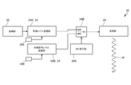
- FIG. 2 is a schematic diagram of the electromagnetic wave transmission device 20 of the present embodiment.
- the electromagnetic wave transmission device 20 has a function of transmitting an electromagnetic wave W indicating a modulation signal that has been multi-valued modulated.
- the electromagnetic wave transmission device 20 includes an acquisition unit 22, a conversion unit 24 (an example of a modulation unit), a switching unit 26A, a selector 26B, a transmission unit 28, a multilevel level setting unit 29A, and a synchronization level. And a setting unit 29B.
- the acquisition unit 22 of the present embodiment has a function of acquiring digital signals such as sounds and images, as an example.
- the acquisition unit 22 also has a function of outputting the acquired digital signal to the conversion unit 24.
- the conversion unit 24 of the present embodiment includes, for example, a multi-value level conversion unit 24A and a synchronization signal level conversion unit 24B.
- the multi-value level conversion unit 24A has a function of receiving a digital signal (communication data) from the acquisition unit 22, converting it to a multi-value level according to the multi-value level setting, and outputting it.
- the multi-value level setting means voltage levels (first voltage values V 2 , V 3 , V 4 ) of two levels or more in a first voltage region RA described later, and a second voltage region RB described later. This means setting of at least one of the voltage level (second voltage value V 1 ) and the voltage value level (third voltage value V 5 ) in the third voltage region described later (see FIG.
- the synchronization signal level conversion unit 24B has a function of outputting a predetermined synchronization signal level according to the synchronization level setting.
- the synchronization level setting means setting of two or more voltage levels in the first voltage region RA, and setting of at least one of the voltage level of the second voltage region RB and the voltage value level of the third voltage region. Means (see FIG. 3).
- the switching unit 26A has a function of generating switching timing of data selected by the selector 26B and output to the transmission unit 28, and inputting the switching timing to the selector 26B.
- the said data are the data (henceforth a multilevel data) which the multi-level conversion part 24A outputs, and the data (henceforth a sync signal data) which the synchronization signal level conversion part 24B outputs.
- the selector 26B has a function of outputting the synchronization signal data and the multilevel data to the transmission unit 28 at different timings according to the switching timing of the data generated by the switching unit 26A.
- the transmitter 28 has a function of oscillating the data selected and input by the selector 26B as an electromagnetic wave W (a terahertz wave as described above in the case of the present embodiment). Therefore, the transmission unit 28 has an element that oscillates a terahertz wave.
- the element that oscillates the terahertz wave of this embodiment is an RTD, for example. However, the element may not be the RTD as long as it is an element that oscillates a terahertz wave.
- FIG. 3 shows the voltage-current characteristics of the RTD of the present embodiment and three levels of first voltage values V 2 , V 3 , and V 4 in the first voltage region RA and the second voltage value V 1 of the second voltage region RB.
- 7 is a graph showing a third voltage value V 5 in the third voltage region RC.
- the RTD has a maximum value and a minimum value located on the higher voltage side than the maximum value in the voltage-current characteristic.
- the voltage value at the maximum value is defined as a voltage value VOL
- the voltage value at the minimum value is defined as a voltage value VOH .
- the spectrum of the current from the voltage value V OL to the voltage value V OH is the differential negative resistance region showing the differential negative resistance characteristic.
- the differential negative resistance region is defined as the first voltage region RA. That is, the RTD has a differential negative resistance region (first voltage region RA) showing a differential negative resistance characteristic in the voltage-current characteristic of its operating region.
- first voltage region RA differential negative resistance region showing a differential negative resistance characteristic in the voltage-current characteristic of its operating region.
- the region on the lower voltage side than the voltage value V OL is lower than the second voltage region RB and the voltage value V OH.
- the region on the high voltage side is defined as the third voltage region RC.
- the RTD is the first voltage value V 2 , V 3 , V 4 in the first voltage region RA, the second voltage value V 1 in the second voltage region RB, and the third voltage value V 5 in the third voltage region RB. It functions as an element that oscillates the electromagnetic wave W when at least one voltage value is applied.
- the transmission unit 28 receives the three levels of the first voltage values V 2 , V 3 , V 4 and the second voltage in the first voltage region RA.
- a synchronization signal having a pattern corresponding to at least one of the second voltage value V 1 in the region RB and the third voltage value V 5 in the third voltage region is transmitted.
- the synchronization signal of the present embodiment is a signal that informs the electromagnetic wave reception device 30 of the detection timing of the transmission signal, and also has a role of causing a part or all of the voltage levels used for the modulation signal to be recognized.
- the transmission unit 28, the multi-valued data from the multi-level conversion unit 24A is input, the first voltage value of the three levels of the first voltage region RA V 2, V 3, V 4 and the second voltage It adapted to transmit a digital signal having a pattern corresponding to at least one of the voltage value of the third voltage value V 5 of the second voltage value V1 and the third voltage region in the region RB.
- the first voltage values V 2 , V 3 , and V 4 in the first voltage region RA are three levels of voltage values as an example, but the first voltage value in the first voltage region RA is It should be at least two levels.
- the first voltage value of the three levels of the first voltage region RA V 2, V 3, V 4 and the second voltage region RB The voltage value is set to at least one of the second voltage value V 1 and the third voltage value V 5 in the third voltage region.
- the electromagnetic wave transmission device 20 of the present embodiment is configured to perform multi-level modulation on multi-valued data and synchronization signal data, and transmit the multi-valued modulated data on the electromagnetic wave W to the electromagnetic wave reception device 30.
- the electromagnetic wave receiving device 30 receives the electromagnetic wave W transmitted by the electromagnetic wave transmitting device 20, and demodulates the received electromagnetic wave W into a digital signal. For example, if the digital signal is a signal obtained by digitizing sound, the electromagnetic wave receiving device 30 generates detection timing based on the synchronization signal data of the electromagnetic wave W received by the electromagnetic wave receiving device 30, and demodulates the digital signal of sound. It is supposed to do.
- the acquisition unit 22 acquires a digital signal related to sound from an external device (not shown) and outputs the acquired digital signal to the conversion unit 24 (multi-value level conversion unit 24A).
- the multi-level conversion unit 24A receives the digital signal (communication data) from the acquisition unit 22, converts it into a multi-level according to the multi-level setting by the multi-level setting unit 29A, and outputs it. Further, the synchronization signal level conversion unit 24B outputs a predetermined synchronization signal level according to the synchronization level setting by the synchronization level setting unit 29B.
- the switching unit 26A generates switching timing between the multi-valued data selected by the selector 26B and output to the transmitting unit 28 and the synchronization signal data, and inputs the switching timing to the selector 26B.
- the selector 26B outputs the synchronization signal data and the multilevel data to the transmission unit 28 at different timings according to the switching timing generated by the switching unit 26A.
- the transmitter 28 transmits the data selected and input by the selector 26B on the electromagnetic wave W. That is, the transmission unit 28 transmits the electromagnetic wave W indicating the modulation signal for the data.
- the electromagnetic wave receiving device 30 receives the electromagnetic wave W transmitted by the transmitting unit 28 (electromagnetic wave transmitting device 20), generates detection timing based on the synchronization signal data of the received electromagnetic wave W, and converts the multivalued data into a digital signal. Demodulate to. As a result, the electromagnetic wave W received by the electromagnetic wave receiving apparatus 30 is demodulated into a sound digital signal.
- V indicates a voltage value and t indicates time.
- V 1 , V 2 , V 3 , V 4 , and V 5 on the axis of the voltage value V are the second voltage value of the second voltage region RB and the first voltage value of the three levels in the first voltage region RA, respectively.
- the 3rd voltage value of the 3rd voltage field RC is shown.
- the patterns of these modulation signals include multilevel data and synchronization signal data.
- V SYNC 4 and V Sync5 of V sync1, V sync2 and V sync3 and 5 of FIG. 4 shows a portion corresponding to the synchronizing signal data of the modulation signal. Further, the entire pattern of FIG.
- the transmission unit 28 transmits the synchronization signal as at least a part of the modulated signal.
- the signal generated by the conversion unit 24 of the present embodiment has two or more levels among the first voltage values V 2 , V 3 , and V 4 in the first voltage region RA.
- the modulation signal uses a voltage value and at least one of the second voltage value V 1 of the second voltage region RB and the third voltage value V 5 of the third voltage region RC. That is, the signal generated by the conversion unit 24 of the present embodiment is a modulation signal that is multivalue-modulated using voltage values of three levels or higher.
- the electromagnetic wave transmission device 20 of the present embodiment can increase the transmission speed as compared with the comparative technique. Accordingly, the electromagnetic communication system 10 of the present embodiment can increase the communication speed as compared with the comparative technique.
- the second voltage region RB and the third voltage region RC are usually set as non-oscillation regions.
- the “non-oscillation region” means a region other than the voltage region for oscillating the electromagnetic wave W in the voltage-current characteristics of the RTD.
- the synchronization signals V sync1, V sync2 , and V sync3 include voltage values of at least one of the second voltage region RB and the third voltage region RC (see FIG. 3). It is set.
- the voltage transition including the voltage values (the second voltage value V 1 and the third voltage value V 5 ) of the second voltage region RB and the third voltage region RC, which are normally the non-oscillation region, is, for example, a normal transition.
- the S/N ratio can be increased as compared with the form in which the voltage transition is made only with the voltage value within the oscillation region (corresponding to the first voltage region RA). Therefore, the electromagnetic wave transmission device 20 of the present embodiment can transmit a signal that is difficult to be erroneously detected to the electromagnetic wave reception device 30.
- the electromagnetic communication system 10 of the present embodiment has high communication stability in terms of recognizability of the synchronization signal.
- the electromagnetic wave transmission device 20 of the present embodiment can increase the transmission speed as compared with the comparative technique, and thus the electromagnetic wave transmission device 20 of the present embodiment has a higher transmission speed than the comparative technique. It is possible to increase the speed and transmit a signal that is difficult to be erroneously detected to the electromagnetic wave receiving device 30.
- the synchronization signal V sync1 has a specific pattern in which the voltage value transits from one of the minimum voltage value (second voltage value V 1 ) and the maximum voltage value (first voltage value V 4 ) to the other. (Pattern in which the voltage values transit in the order of description of V 1 , V 2 , V 3 , and V 4 or a pattern in which the voltage values transit in the reverse order of description). That is, the synchronization signal V sync1 of this embodiment includes a maximum voltage value (first voltage value V 4) and the minimum voltage value among the voltage setting level in the first voltage region RA (second voltage value V 1) It is a pattern.
- the electromagnetic wave receiving device 30 of the present embodiment recognizes the maximum voltage value and the minimum voltage value of the received modulated signal.
- the digital signal is multilevel-modulated using the voltage values V 1 , V 2 , V 3 , and V 4 .
- the synchronization signal V sync3 a particular pattern (V whose voltage value changes over from one to the other of the minimum voltage value (first voltage value V 2) and the maximum voltage value (third voltage value V 5) 2 , V 3 , V 4 and V 5 are set in a pattern in which the voltage values transit in the order described or a pattern in which the voltage values transit in the reverse order in which they are described).
- Synchronizing signal V sync2 a particular pattern whose voltage value changes over from one to the other of the minimum voltage value (first voltage value V 2) and the maximum voltage value (second voltage value V 1) (V 2, V 3 , V 4 and V 1 are set in a pattern in which the voltage values transit in the order of description, or vice versa.
- the digital signal is multilevel-modulated using the voltage values V 2 , V 3 , V 4 , and V 5 . Therefore, the electromagnetic wave transmission device 20 of the present embodiment can transmit the synchronization signal that is easily recognized by the electromagnetic wave reception device 30.
- the electromagnetic communication system 10 of the present embodiment has high communication stability in terms of recognizability of the synchronization signal.
- the synchronization signals V sync4 and V sync5 in FIG. 5 have any voltage value (second voltage value V 1 ) in the second voltage region RB and the third voltage region RC (see FIG. 3) which are the normal non-oscillation regions.
- a third voltage value V 5 ) and four levels, which are all levels, are set as the multi-valued levels that the digital signal can take. Therefore, in this embodiment, by using such a synchronization signal, the level voltage of the synchronization signal can be transmitted to the electromagnetic wave transmission device 20 as teacher data. Further, in the electromagnetic wave receiving device 30, it becomes possible to extract each level voltage from the synchronization signal and set the level of the multi-valued data of the reception signal. Therefore, the electromagnetic wave transmission device 20 of the present embodiment can cause the electromagnetic wave reception device 30 to recognize the level voltage of the modulated signal.
- the modulation signal may be generated using both voltage values of the third voltage value V 5 in the third voltage region.
- a signal that transitions from any one of the first voltage values V 2 , V 3 , and V 4 to the second voltage value V 1 and one of the first voltage values V 2 , V 3 , and V 4 The signal transitioning from one voltage value to the third voltage value V 5 is the same signal.
- the multi-level conversion unit 24A (conversion unit 24) of the present embodiment converts the voltage value of any one of the first voltage values V 2 , V 3 , and V 4 into the second voltage value V 1 and the second voltage value V 1 .
- the signal is transited to any one of the three voltage values V 5 , the signal is transited to the shorter transition time.
- the multi-level conversion unit 24A determines that the second transition time is shorter. The signal is transited to the voltage value V 1 .
- the multi-level conversion unit 24A is set to have a shorter transition time.
- the signal is transited to the third voltage value V 5 . Therefore, the present embodiment shortens the transition time as described above when the modulation signal is generated using the voltage value of the first voltage region RA and the voltage values of both the second voltage region RB and the third voltage region. By doing so, the transmission speed (communication speed) can be further increased.
- the present invention has been described by taking the present embodiment as an example, but the present invention is not limited to the present embodiment.
- the technical scope of the present invention includes, for example, the following forms (modifications).
- three levels of voltage values in the first voltage region RA have been described as set voltage levels.
- the set voltage level in the first voltage region RA may be two levels or more.
- the pattern of the synchronization signal has described the pattern of the synchronization signal as V sync4, V sync5 of V sync1, V sync2, V sync3 and 5 of FIG. 4, the pattern of the synchronization signal be different from these patterns Good.
- the pattern of the synchronization signal has been described V sync4, V sync5 of V sync1, V sync2, V sync3 and 5 of FIG. 4 as an example.
- any form that includes any one of these sync signal patterns or a modification thereof may be used.
- the synchronization signal includes (1) a signal that includes the second voltage value V 1 of the second voltage region RB and does not include the third voltage value V 5 of the third voltage region RC, and (2) a signal of the second voltage region RB.
- the multi-level conversion unit 24A of the present embodiment is configured such that any one of the first voltage values V 2 , V 3 , and V 4 to the second voltage value V 1 and the third voltage value V 5 is used.
- the signal is transited to one side, the signal is transited to the one in which the transition time becomes shorter.
- the first voltage value V 1 passes through one of the second voltage value V 1 and the third voltage value V 5 from any one of the first voltage values V 2 , V 3 , and V 4.
- the signal may be transited to the shorter transition time.
- the transition time is shortened as described above. By doing so, the transmission speed (communication speed) can be further increased.
- electromagnetic wave communication system 20 electromagnetic wave transmission device 22 acquisition unit 24 conversion unit (an example of a modulation unit) 24A multi-level conversion unit 24B synchronization signal level conversion unit 26A switching unit 26B selector 28 transmission unit 29A multi-level level setting unit 29B synchronization level setting unit 30 electromagnetic wave reception device RA first voltage region RB second voltage region RC third voltage Region W Electromagnetic wave (an example of terahertz wave)
Landscapes
- Engineering & Computer Science (AREA)
- Computer Networks & Wireless Communication (AREA)
- Signal Processing (AREA)
- Transmitters (AREA)
- Dc Digital Transmission (AREA)
- Synchronisation In Digital Transmission Systems (AREA)
Abstract
本発明の電磁波送信装置は、電圧-電流特性が極大値及び前記極大値よりも高電圧側に位置する極小値を有し、かつ、変調信号を示す電磁波を送信する送信部と、デジタル信号を取得する取得部と、前記デジタル信号を、前記極大値の電圧以上で前記極小値の電圧以下の電圧領域とされる第1電圧領域の2水準以上の第1電圧値、並びに、前記極大値の電圧未満の電圧領域とされる第2電圧領域の第2電圧値及び前記極小値の電圧より高電圧側の電圧領域とされる第3電圧領域の第3電圧値の少なくとも一方を用いた信号であって、前記変調信号に変調する変調部と、を備える。
Description
本発明は、電磁波送信装置及び電磁波通信システムに関する。
電磁波送信用の発振素子に用いた通信用の変調方式として、振幅偏移変調方式(Amplitude-Shift keying変調方式、以下、ASK変調方式という。)が知られている。また、通信用の変調方式としてオンオフ変調方式(Оn Оff keying変調方式、以下、OOK変調方式)も、ASK変調方式に含まれる1つの方式として知られている。
ここで、特許文献1には、共鳴トンネルダイオード(Resonant Tunneling Diode、以下、RTDという。)を電磁波送信用の発振素子として用いたASK変調方式に関する技術が開示されている。具体的には、当該技術は、RTDの発振領域のデータ(例えばOnに相当する信号)と、非発振領域のデータ(例えばOffに相当する信号)とを切り替えることにより2値を表す技術、すなわち、振幅の違いでOn及びOffを表す技術とされている。
また、特許文献2には、RTD等の連続発振のテラヘルツ波を用いたASK変調方式に関する技術が開示されている。具体的には、当該技術は、強度が可変な可変光を信号光として変調素子に重畳的に入射させ、信号強度に応じてテラヘルツ波の振幅を変調する技術とされている。
また、特許文献2には、RTD等の連続発振のテラヘルツ波を用いたASK変調方式に関する技術が開示されている。具体的には、当該技術は、強度が可変な可変光を信号光として変調素子に重畳的に入射させ、信号強度に応じてテラヘルツ波の振幅を変調する技術とされている。
しかしながら、特許文献1及び特許文献2に開示されている技術は、振幅の違いにより2値を表す技術であることから、送信速度(又は通信速度)の高速化に限界がある。
本発明が解決しようとする課題としては、送信速度を高速化することが一例として挙げられる。
請求項1に記載の発明は、
電圧-電流特性が極大値及び前記極大値よりも高電圧側に位置する極小値を有し、かつ、変調信号を示す電磁波を送信する送信部と、
デジタル信号を取得する取得部と、
前記デジタル信号を、前記極大値の電圧以上で前記極小値の電圧以下の電圧領域とされる第1電圧領域の2水準以上の第1電圧値、並びに、前記極大値の電圧未満の電圧領域とされる第2電圧領域の第2電圧値及び前記極小値の電圧より高電圧側の電圧領域とされる第3電圧領域の第3電圧値の少なくとも一方を用いた信号であって、前記変調信号に変調する変調部と、
を備える電磁波送信装置である。
電圧-電流特性が極大値及び前記極大値よりも高電圧側に位置する極小値を有し、かつ、変調信号を示す電磁波を送信する送信部と、
デジタル信号を取得する取得部と、
前記デジタル信号を、前記極大値の電圧以上で前記極小値の電圧以下の電圧領域とされる第1電圧領域の2水準以上の第1電圧値、並びに、前記極大値の電圧未満の電圧領域とされる第2電圧領域の第2電圧値及び前記極小値の電圧より高電圧側の電圧領域とされる第3電圧領域の第3電圧値の少なくとも一方を用いた信号であって、前記変調信号に変調する変調部と、
を備える電磁波送信装置である。
上述した目的、およびその他の目的、特徴および利点は、以下に述べる好適な実施の形態、およびそれに付随する以下の図面によってさらに明らかになる。
<概要>
以下、本実施形態(本発明の一例)について説明する。まず、本実施形態の電磁波通信システム10(図1参照)の機能及び構成について図面を参照しながら説明する。次いで、本実施形態の電磁波通信システム10の動作について図面を参照しながら説明する。本実施形態の効果については、動作についての説明の中で説明する。なお、参照するすべての図面では同様の機能を有する構成要素に同様の符号を付し、明細書では適宜説明を省略する。
以下、本実施形態(本発明の一例)について説明する。まず、本実施形態の電磁波通信システム10(図1参照)の機能及び構成について図面を参照しながら説明する。次いで、本実施形態の電磁波通信システム10の動作について図面を参照しながら説明する。本実施形態の効果については、動作についての説明の中で説明する。なお、参照するすべての図面では同様の機能を有する構成要素に同様の符号を付し、明細書では適宜説明を省略する。
<構成>
図1は、本実施形態の電磁波通信システム10の概略図である。電磁波通信システム10は、電磁波送信装置20と、電磁波受信装置30とを備えている。電磁波通信システム10は、電磁波送信装置20により送信される電磁波Wを、電磁波受信装置30により受信する機能を有する。
図1は、本実施形態の電磁波通信システム10の概略図である。電磁波通信システム10は、電磁波送信装置20と、電磁波受信装置30とを備えている。電磁波通信システム10は、電磁波送信装置20により送信される電磁波Wを、電磁波受信装置30により受信する機能を有する。
本実施形態の電磁波Wには、後述する変調信号を示す電磁波とされている。また、本実施形態の電磁波Wは、一例として、テラヘルツ波とされている。ここで、テラヘルツ波とは、ミリ波よりも短波長で赤外線よりも長波長の電磁波と言われている。テラヘルツ波は、光波及び電波の両方の性質を兼ね備えていた電磁波であり、例えば、布、紙、木、プラスチック、陶磁器等を透過し(又は透過し易く)、金属、水等は透過しない(又は透過し難い)という性質を有する。一般的に、テラヘルツ波の周波数は1THz前後(波長は300μm前後に相当)の電磁波とも言われているが、その範囲について一般的に明確な定義はない。そこで、本明細書では、テラヘルツ波の波長の範囲を70GHz以上10THz以下の範囲と定義する。
〔電磁波送信装置〕
図2は、本実施形態の電磁波送信装置20の概略図である。電磁波送信装置20は、多値変調された変調信号を示す電磁波Wを送信する機能を有する。電磁波送信装置20は、一例として、取得部22と、変換部24(変調部の一例)と、切り替え部26Aと、選択器26Bと、送信部28と、多値レベル設定部29Aと、同期レベル設定部29Bとを備えている。
図2は、本実施形態の電磁波送信装置20の概略図である。電磁波送信装置20は、多値変調された変調信号を示す電磁波Wを送信する機能を有する。電磁波送信装置20は、一例として、取得部22と、変換部24(変調部の一例)と、切り替え部26Aと、選択器26Bと、送信部28と、多値レベル設定部29Aと、同期レベル設定部29Bとを備えている。
(取得部)
本実施形態の取得部22は、一例として音、映像等のデジタル信号を取得する機能を有する。また、取得部22は、取得したデジタル信号を、変換部24に出力する機能を有する。
本実施形態の取得部22は、一例として音、映像等のデジタル信号を取得する機能を有する。また、取得部22は、取得したデジタル信号を、変換部24に出力する機能を有する。
(変換部)
本実施形態の変換部24は、一例として、多値レベル変換部24Aと、同期信号レベル変換部24Bとを有している。
多値レベル変換部24Aは、取得部22からのデジタル信号(通信用データ)を入力とし、多値レベル設定に従い、多値レベルに変換して出力する機能を有する。ここで、多値レベル設定とは、後述する第1電圧領域RA内の2水準以上の電圧レベル(第1電圧値V2、V3、V4)、並びに、後述する第2電圧領域RBの電圧レベル(第2電圧値V1)及び後述する第3電圧領域の電圧値レベル(第3電圧値V5)の少なくとも一方の電圧レベルの設定を意味する(図3参照)。
また、同期信号レベル変換部24Bは、同期レベル設定に従い、所定の同期信号レベルを出力する機能を有する。ここで、同期レベル設定とは、第1電圧領域RA内の2水準以上の電圧レベル、並びに、第2電圧領域RBの電圧レベル及び第3電圧領域の電圧値レベルの少なくとも一方の電圧レベルの設定を意味する(図3参照)。
本実施形態の変換部24は、一例として、多値レベル変換部24Aと、同期信号レベル変換部24Bとを有している。
多値レベル変換部24Aは、取得部22からのデジタル信号(通信用データ)を入力とし、多値レベル設定に従い、多値レベルに変換して出力する機能を有する。ここで、多値レベル設定とは、後述する第1電圧領域RA内の2水準以上の電圧レベル(第1電圧値V2、V3、V4)、並びに、後述する第2電圧領域RBの電圧レベル(第2電圧値V1)及び後述する第3電圧領域の電圧値レベル(第3電圧値V5)の少なくとも一方の電圧レベルの設定を意味する(図3参照)。
また、同期信号レベル変換部24Bは、同期レベル設定に従い、所定の同期信号レベルを出力する機能を有する。ここで、同期レベル設定とは、第1電圧領域RA内の2水準以上の電圧レベル、並びに、第2電圧領域RBの電圧レベル及び第3電圧領域の電圧値レベルの少なくとも一方の電圧レベルの設定を意味する(図3参照)。
(切り替え部及び選択部)
切り替え部26Aは、選択器26Bによって選択されて送信部28に出力されるデータの切り替えタイミングを生成して、選択器26Bに入力する機能を有する。ここで、当該データとは、多値レベル変換部24Aが出力するデータ(以下、多値データという。)及び同期信号レベル変換部24Bが出力するデータ(以下、同期信号データという。)である。
選択器26Bは、切り替え部26Aが生成したデータの切り替えタイミングに従い、同期信号データと多値データとを異なるタイミングで送信部28に出力する機能を有する。
切り替え部26Aは、選択器26Bによって選択されて送信部28に出力されるデータの切り替えタイミングを生成して、選択器26Bに入力する機能を有する。ここで、当該データとは、多値レベル変換部24Aが出力するデータ(以下、多値データという。)及び同期信号レベル変換部24Bが出力するデータ(以下、同期信号データという。)である。
選択器26Bは、切り替え部26Aが生成したデータの切り替えタイミングに従い、同期信号データと多値データとを異なるタイミングで送信部28に出力する機能を有する。
(送信部)
送信部28は、選択器26Bにより選択されて入力されるデータを電磁波W(本実施形態の場合は前述のとおりテラヘルツ波)として発振する機能を有する。そのため、送信部28は、テラヘルツ波を発振する素子を有している。本実施形態のテラヘルツ波を発振する素子は、一例としてRTDとされている。ただし、テラヘルツ波を発振する素子であれば、当該素子はRTDでなくてもよい。
送信部28は、選択器26Bにより選択されて入力されるデータを電磁波W(本実施形態の場合は前述のとおりテラヘルツ波)として発振する機能を有する。そのため、送信部28は、テラヘルツ波を発振する素子を有している。本実施形態のテラヘルツ波を発振する素子は、一例としてRTDとされている。ただし、テラヘルツ波を発振する素子であれば、当該素子はRTDでなくてもよい。
ここで、RTDの電圧-電流特性(電圧と電流との関係を示す2次元のグラフにおける、電圧に対する電流の特性)について図3のグラフを参照しながら説明する。図3は、本実施形態のRTDの電圧-電流特性及び第1電圧領域RA内の3水準の第1電圧値V2、V3、V4並びに第2電圧領域RBの第2電圧値V1及び第3電圧領域RCの第3電圧値V5を示すグラフである。
RTDは、電圧-電流特性において、極大値及び前記極大値よりも高電圧側に位置する極小値を有する。ここで、当該極大値における電圧値を電圧値VOLとし、当該極小値における電圧値を電圧値VOHと定義する。そして、電圧値VOLから電圧値VOHに亘る電流のスペクトルは、微分負性抵抗特性を示す微分負性抵抗領域とされている。本明細書では、当該微分負性抵抗領域を第1電圧領域RAと定義する。すなわち、RTDは、その動作領域の電圧-電流特性に、微分負性抵抗特性を示す微分負性抵抗領域(第1電圧領域RA)を有する。また、本明細書では、電圧-電流特性のグラフにおける第1電圧領域RAの両側の電圧領域のうち電圧値VOLよりも低電圧側の領域を第2電圧領域RB、電圧値VOHよりも高電圧側の領域を第3電圧領域RCと定義する。そして、RTDは、第1電圧領域RA内の第1電圧値V2、V3、V4並びに第2電圧領域RBの第2電圧値V1及び第3電圧領域の第3電圧値V5の少なくとも一方の電圧値が印加されている場合に、電磁波Wを発振する素子として機能するようになっている。
RTDは、電圧-電流特性において、極大値及び前記極大値よりも高電圧側に位置する極小値を有する。ここで、当該極大値における電圧値を電圧値VOLとし、当該極小値における電圧値を電圧値VOHと定義する。そして、電圧値VOLから電圧値VOHに亘る電流のスペクトルは、微分負性抵抗特性を示す微分負性抵抗領域とされている。本明細書では、当該微分負性抵抗領域を第1電圧領域RAと定義する。すなわち、RTDは、その動作領域の電圧-電流特性に、微分負性抵抗特性を示す微分負性抵抗領域(第1電圧領域RA)を有する。また、本明細書では、電圧-電流特性のグラフにおける第1電圧領域RAの両側の電圧領域のうち電圧値VOLよりも低電圧側の領域を第2電圧領域RB、電圧値VOHよりも高電圧側の領域を第3電圧領域RCと定義する。そして、RTDは、第1電圧領域RA内の第1電圧値V2、V3、V4並びに第2電圧領域RBの第2電圧値V1及び第3電圧領域の第3電圧値V5の少なくとも一方の電圧値が印加されている場合に、電磁波Wを発振する素子として機能するようになっている。
そして、送信部28は、同期信号レベル変換部24Bからの同期信号データが入力されると、第1電圧領域RA内の3水準の第1電圧値V2、V3、V4並びに第2電圧領域RBの第2電圧値V1及び第3電圧領域の第3電圧値V5の少なくとも一方の電圧値に対応したパターンを有する同期信号を送信するようになっている。ここで、本実施形態の同期信号は、電磁波受信装置30に、送信信号の検出タイミングを知らせる信号であり、また、変調信号に使用される一部又はすべての電圧レベルを認識させる役割を有する。次いで、送信部28は、多値レベル変換部24Aからの多値データが入力されると、第1電圧領域RA内の3水準の第1電圧値V2、V3、V4並びに第2電圧領域RBの第2電圧値V1及び第3電圧領域の第3電圧値V5の少なくとも一方の電圧値に対応したパターンを有するデジタル信号を送信するようになっている。ここで、本実施形態では第1電圧領域RA内の第1電圧値V2、V3、V4を一例として3水準の電圧値としているが、第1電圧領域RA内の第1電圧値は2水準以上であればよい。
以上のとおりであるから、本実施形態における多値レベル設定及び同期レベル設定は、第1電圧領域RA内の3水準の第1電圧値V2、V3、V4並びに第2電圧領域RBの第2電圧値V1及び第3電圧領域の第3電圧値V5の少なくとも一方の電圧値に設定されている。また、本実施形態の電磁波送信装置20は、多値データ及び同期信号データを多値変調し、多値変調したデータを電磁波Wに乗せて電磁波受信装置30に送信するようになっている。
〔電磁波受信装置〕
電磁波受信装置30は、電磁波送信装置20が送信した電磁波Wを受信し、受信した電磁波Wをデジタル信号に復調するようになっている。例えば、デジタル信号が音をデジタル化した信号であれば、電磁波受信装置30は電磁波受信装置30により受信された電磁波Wのうちの同期信号データに基づき検出タイミングを生成し、音のデジタル信号を復調するようになっている。
電磁波受信装置30は、電磁波送信装置20が送信した電磁波Wを受信し、受信した電磁波Wをデジタル信号に復調するようになっている。例えば、デジタル信号が音をデジタル化した信号であれば、電磁波受信装置30は電磁波受信装置30により受信された電磁波Wのうちの同期信号データに基づき検出タイミングを生成し、音のデジタル信号を復調するようになっている。
以上が、本実施形態の構成についての説明である。
<動作>
次に、本実施形態の電磁波通信システム10の動作について図面を参照しながら説明する。以下、まず、全体の流れについて説明し、次いで多値変調の具体例を挙げて説明する。なお、電磁波通信システム10により一例として音に関する信号を通信する場合とする。また前述のとおり、以下の説明とともに本実施形態の効果についても説明する。
次に、本実施形態の電磁波通信システム10の動作について図面を参照しながら説明する。以下、まず、全体の流れについて説明し、次いで多値変調の具体例を挙げて説明する。なお、電磁波通信システム10により一例として音に関する信号を通信する場合とする。また前述のとおり、以下の説明とともに本実施形態の効果についても説明する。
〔全体の流れ〕
以下、本実施形態の動作の全体の流れについて図1及び図2を参照しながら説明する。
まず、取得部22は、外部装置(図示省略)から音に関するデジタル信号を取得し、取得したデジタル信号を変換部24(多値レベル変換部24A)に出力する。
以下、本実施形態の動作の全体の流れについて図1及び図2を参照しながら説明する。
まず、取得部22は、外部装置(図示省略)から音に関するデジタル信号を取得し、取得したデジタル信号を変換部24(多値レベル変換部24A)に出力する。
次いで、多値レベル変換部24Aは、取得部22からのデジタル信号(通信用データ)を入力とし、多値レベル設定部29Aによる多値レベル設定に従い、多値レベルに変換して出力する。また、同期信号レベル変換部24Bは、同期レベル設定部29Bによる同期レベル設定に従い、所定の同期信号レベルを出力する。
次いで、切り替え部26Aは、選択器26Bによって選択されて送信部28に出力される多値データと同期信号データとの切り替えタイミングを生成して、選択器26Bに入力する。その結果、選択器26Bは、切り替え部26Aが生成した切り替えタイミングに従い、同期信号データと多値データとを異なるタイミングで送信部28に出力する。
次いで、送信部28は、選択器26Bにより選択されて入力されるデータを電磁波Wに乗せて送信する。すなわち、送信部28は、当該データについての変調信号を示す電磁波Wを送信する。
次いで、電磁波受信装置30は、送信部28(電磁波送信装置20)が送信した電磁波Wを受信し、受信した電磁波Wのうちの同期信号データに基づき検出タイミングを生成し、多値データをデジタル信号に復調する。その結果、電磁波受信装置30により受信された電磁波Wは音のデジタル信号に復調される。
以上が、本実施形態の動作の全体の流れについての説明である。
〔多値変調の具体例〕
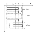
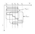
次に、図3、図4及び図5を参照しながら、変調信号の具体例について説明する。図4及び図5は、それぞれ、本実施形態の電磁波送信装置20が送信する変調信号の一例である。
次に、図3、図4及び図5を参照しながら、変調信号の具体例について説明する。図4及び図5は、それぞれ、本実施形態の電磁波送信装置20が送信する変調信号の一例である。
ここで、図4及び図5における、Vは電圧値、tは時間を示す。電圧値Vの軸における、V1、V2、V3、V4、V5は、それぞれ第2電圧領域RBの第2電圧値、第1電圧領域RA内の3水準の第1電圧値、第3電圧領域RCの第3電圧値を示す。これらの変調信号のパターンは、多値データ及び同期信号データを含む。
なお、図4のVsync1、Vsync2及びVsync3並びに図5のVsync4及びVsync5は、変調信号のうち同期信号データに相当する部分を示す。また、図5の全体のパターンは、同期信号データに相当する部分とそれ以外の部分(変調データに相当する部分)とを含む変調信号を示す。すなわち、本実施形態では、送信部28は変調信号のうちの少なくとも一部として同期信号を送信する。
なお、図4のVsync1、Vsync2及びVsync3並びに図5のVsync4及びVsync5は、変調信号のうち同期信号データに相当する部分を示す。また、図5の全体のパターンは、同期信号データに相当する部分とそれ以外の部分(変調データに相当する部分)とを含む変調信号を示す。すなわち、本実施形態では、送信部28は変調信号のうちの少なくとも一部として同期信号を送信する。
本実施形態の変換部24が生成する信号は、図4及び図5に示されるように、第1電圧領域RA内の第1電圧値V2、V3、V4のうちの2水準以上の電圧値並びに第2電圧領域RBの第2電圧値V1及び第3電圧領域RCの第3電圧値V5の少なくとも一方の電圧値を用いた変調信号とされている。すなわち、本実施形態の変換部24が生成する信号は、3水準以上の電圧値を用いて多値変調された変調信号とされる。具体的には、当該変調信号は、例えば、mビット(m≧1、本実施形態の場合は一例としてm=2)のデータをn値(n≧3、本実施形態の場合は一例としてn=4)の電圧レベルに変換して多値変調された信号とされる。そのため、本実施形態の場合、前述の特許文献1及び2に開示されている技術(以下、比較技術という。)に比べて、同じ時間で送信できるデータの量が多い。
したがって、本実施形態の電磁波送信装置20は、比較技術に比べて、送信速度を高速化することができる。これに伴い、本実施形態の電磁波通信システム10は、比較技術に比べて、通信速度を高速化することができる。
したがって、本実施形態の電磁波送信装置20は、比較技術に比べて、送信速度を高速化することができる。これに伴い、本実施形態の電磁波通信システム10は、比較技術に比べて、通信速度を高速化することができる。
第2電圧領域RB及び第3電圧領域RCは、通常、非発振領域とすることが通常とされている。「非発振領域」とは、RTDの電圧-電流特性において電磁波Wを発振するための電圧領域以外の領域を意味する。
しかしながら、図4に示されるように、本実施形態では、同期信号Vsync1、Vsync2、Vsync3に第2電圧領域RB及び第3電圧領域RC(図3参照)の少なくとも一方の電圧値を含む設定としている。そして、通常、非発振領域とされる第2電圧領域RB及び第3電圧領域RCの電圧値(第2電圧値V1及び第3電圧値V5)を含んだ電圧遷移は、例えば、通常の発振領域(第1電圧領域RAに相当)内のみの電圧値で電圧遷移する形態に比べて、S/N比を大きくすることができる。
したがって、本実施形態の電磁波送信装置20は、電磁波受信装置30に誤検出され難い信号を送信することができる。これに伴い、本実施形態の電磁波通信システム10は、同期信号の認識性の点で通信の安定性が高い。また、前述のとおり、本実施形態の電磁波送信装置20は比較技術に比べて送信速度を高速化することができることから、本実施形態の電磁波送信装置20は、比較技術に比べて、送信速度を高速化したうえで、電磁波受信装置30に誤検出され難い信号を送信することができる。
しかしながら、図4に示されるように、本実施形態では、同期信号Vsync1、Vsync2、Vsync3に第2電圧領域RB及び第3電圧領域RC(図3参照)の少なくとも一方の電圧値を含む設定としている。そして、通常、非発振領域とされる第2電圧領域RB及び第3電圧領域RCの電圧値(第2電圧値V1及び第3電圧値V5)を含んだ電圧遷移は、例えば、通常の発振領域(第1電圧領域RAに相当)内のみの電圧値で電圧遷移する形態に比べて、S/N比を大きくすることができる。
したがって、本実施形態の電磁波送信装置20は、電磁波受信装置30に誤検出され難い信号を送信することができる。これに伴い、本実施形態の電磁波通信システム10は、同期信号の認識性の点で通信の安定性が高い。また、前述のとおり、本実施形態の電磁波送信装置20は比較技術に比べて送信速度を高速化することができることから、本実施形態の電磁波送信装置20は、比較技術に比べて、送信速度を高速化したうえで、電磁波受信装置30に誤検出され難い信号を送信することができる。
また、図4における、同期信号Vsync1は、電圧値が最小電圧値(第2電圧値V1)及び最大電圧値(第1電圧値V4)の一方から他方に亘って遷移する特定のパターン(V1、V2、V3、V4の記載順で電圧値が遷移するパターン又はこの逆の記載順で電圧値が遷移するパターン)に設定されている。すなわち、本実施形態の同期信号Vsync1は、第1電圧領域RA内の電圧設定レベルのうちの最大電圧値(第1電圧値V4)及び最小電圧値(第2電圧値V1)を含むパターンとされる。そのため、本実施形態の電磁波受信装置30には、受信する変調信号の最大電圧値及び最小電圧値が認識される。なお、デジタル信号は、電圧値V1、V2、V3、V4を用いて多値変調される。
図4における、同期信号Vsync3は、電圧値が最小電圧値(第1電圧値V2)及び最大電圧値(第3電圧値V5)の一方から他方に亘って遷移する特定のパターン(V2、V3、V4、V5の記載順で電圧値が遷移するパターン又はこの逆の記載順で電圧値が遷移するパターン)に設定されている。同期信号Vsync2は、電圧値が最小電圧値(第1電圧値V2)及び最大電圧値(第2電圧値V1)の一方から他方に亘って遷移する特定のパターン(V2、V3、V4、V1の記載順で電圧値が遷移するパターン又はこの逆の記載順で電圧値が遷移するパターン)に設定されている。なお、デジタル信号は、電圧値V2、V3、V4、V5用いて多値変調される。
したがって、本実施形態の電磁波送信装置20は、電磁波受信装置30に認識され易い同期信号を送信することができる。これに伴い、本実施形態の電磁波通信システム10は、同期信号の認識性の点で通信の安定性が高い。
図4における、同期信号Vsync3は、電圧値が最小電圧値(第1電圧値V2)及び最大電圧値(第3電圧値V5)の一方から他方に亘って遷移する特定のパターン(V2、V3、V4、V5の記載順で電圧値が遷移するパターン又はこの逆の記載順で電圧値が遷移するパターン)に設定されている。同期信号Vsync2は、電圧値が最小電圧値(第1電圧値V2)及び最大電圧値(第2電圧値V1)の一方から他方に亘って遷移する特定のパターン(V2、V3、V4、V1の記載順で電圧値が遷移するパターン又はこの逆の記載順で電圧値が遷移するパターン)に設定されている。なお、デジタル信号は、電圧値V2、V3、V4、V5用いて多値変調される。
したがって、本実施形態の電磁波送信装置20は、電磁波受信装置30に認識され易い同期信号を送信することができる。これに伴い、本実施形態の電磁波通信システム10は、同期信号の認識性の点で通信の安定性が高い。
また、図5における同期信号Vsync4、Vsync5は、通常の非発振領域とされる第2電圧領域RB及び第3電圧領域RC(図3参照)のいずれの電圧値(第2電圧値V1及び第3電圧値V5)を含み、デジタル信号が取り得る多値レベルとしてすべてのレベルとなる4レベルを用いるように設定されている。そのため、本実施形態では、このような同期信号とすることで、同期信号のレベル電圧を教師データとして電磁波送信装置20に送信することが可能となる。また、電磁波受信装置30においては同期信号から各レベル電圧を抽出し、受信信号の多値データのレベルを設定することが可能となる。
したがって、本実施形態の電磁波送信装置20は、電磁波受信装置30に、変調信号のレベル電圧を認識させることができる。
したがって、本実施形態の電磁波送信装置20は、電磁波受信装置30に、変調信号のレベル電圧を認識させることができる。
また、本実施形態の場合、第1電圧領域RA内の第1電圧値V2、V3、V4のうちの2水準以上の電圧値並びに第2電圧領域RBの第2電圧値V1及び第3電圧領域の第3電圧値V5の両方の電圧値を用いて変調信号を生成してもよい。
この場合、第1電圧値V2、V3、V4のいずれか1つの電圧値から第2電圧値V1に遷移する信号と、第1電圧値V2、V3、V4のいずれか1つの電圧値から第3電圧値V5に遷移する信号とは、同じ信号を示すとする。
そして、この場合、本実施形態の多値レベル変換部24A(変換部24)は、第1電圧値V2、V3、V4のいずれか1つの電圧値から第2電圧値V1及び第3電圧値V5のいずれか一方に信号を遷移させる場合、遷移時間が短くなる方に信号を遷移させる。例えば、第1電圧値V2、V3、V4のいずれか1つの電圧値が第1電圧値V2である場合、多値レベル変換部24Aは遷移時間が短くなる方とされる第2電圧値V1に信号を遷移させる。また、例えば、第1電圧値V2、V3、V4のいずれか1つの電圧値が第1電圧値V4である場合、多値レベル変換部24Aは遷移時間が短くなる方とされる第3電圧値V5に信号を遷移させる。
したがって、本実施形態は、第1電圧領域RAの電圧値並びに第2電圧領域RB及び第3電圧領域の両方の電圧値を用いて変調信号を生成する場合に上記のようにして遷移時間を短くすることにより、送信速度(通信速度)をより高速化することができる。
この場合、第1電圧値V2、V3、V4のいずれか1つの電圧値から第2電圧値V1に遷移する信号と、第1電圧値V2、V3、V4のいずれか1つの電圧値から第3電圧値V5に遷移する信号とは、同じ信号を示すとする。
そして、この場合、本実施形態の多値レベル変換部24A(変換部24)は、第1電圧値V2、V3、V4のいずれか1つの電圧値から第2電圧値V1及び第3電圧値V5のいずれか一方に信号を遷移させる場合、遷移時間が短くなる方に信号を遷移させる。例えば、第1電圧値V2、V3、V4のいずれか1つの電圧値が第1電圧値V2である場合、多値レベル変換部24Aは遷移時間が短くなる方とされる第2電圧値V1に信号を遷移させる。また、例えば、第1電圧値V2、V3、V4のいずれか1つの電圧値が第1電圧値V4である場合、多値レベル変換部24Aは遷移時間が短くなる方とされる第3電圧値V5に信号を遷移させる。
したがって、本実施形態は、第1電圧領域RAの電圧値並びに第2電圧領域RB及び第3電圧領域の両方の電圧値を用いて変調信号を生成する場合に上記のようにして遷移時間を短くすることにより、送信速度(通信速度)をより高速化することができる。
以上のとおり、本発明について本実施形態を一例として説明したが、本発明は本実施形態に限定されるものではない。本発明の技術的範囲には、例えば、下記のような形態(変形例)も含まれる。
例えば、本実施形態では、第1電圧領域RA内に3水準の電圧値を設定電圧レベルとして説明した。しかしながら、第1電圧領域RA内の設定電圧レベルは2水準以上であればよい。
また、本実施形態では、同期信号のパターンを図4のVsync1、Vsync2、Vsync3及び図5のVsync4、Vsync5として説明したが、同期信号のパターンはこれらと異なるパターンであってもよい。
なお、本実施形態の説明では、同期信号のパターンを、図4のVsync1、Vsync2、Vsync3及び図5のVsync4、Vsync5を例として説明した。しかしながら、本発明の技術的範囲に属する形態としては、これらの同期信号のパターンのいずれか1つ又はその変形を含む形態であればよい。すなわち、同期信号は、(1)第2電圧領域RBの第2電圧値V1を含み、第3電圧領域RCの第3電圧値V5を含まない信号、(2)第2電圧領域RBの第2電圧値V1を含まず、第3電圧領域RCの第3電圧値V5を含む信号並びに(3)第2電圧領域RBの第2電圧値V1及び第3電圧領域RCの第3電圧値V5を含む信号のいずれか1つであればよい。
なお、本実施形態の説明では、同期信号のパターンを、図4のVsync1、Vsync2、Vsync3及び図5のVsync4、Vsync5を例として説明した。しかしながら、本発明の技術的範囲に属する形態としては、これらの同期信号のパターンのいずれか1つ又はその変形を含む形態であればよい。すなわち、同期信号は、(1)第2電圧領域RBの第2電圧値V1を含み、第3電圧領域RCの第3電圧値V5を含まない信号、(2)第2電圧領域RBの第2電圧値V1を含まず、第3電圧領域RCの第3電圧値V5を含む信号並びに(3)第2電圧領域RBの第2電圧値V1及び第3電圧領域RCの第3電圧値V5を含む信号のいずれか1つであればよい。
また、本実施形態の多値レベル変換部24Aは、第1電圧値V2、V3、V4のいずれか1つの電圧値から第2電圧値V1及び第3電圧値V5のいずれか一方に信号を遷移させる場合、遷移時間が短くなる方に信号を遷移させるとして説明した。しかしながら、例えば、以下のようにしてもよい。具体的には、第1電圧値V2、V3、V4のいずれか1つの電圧値から第2電圧値V1及び第3電圧値V5のいずれか一方を経由して第1電圧値V2、V3、V4のいずれか1つの電圧値に信号を遷移させる場合、遷移時間が短くなる方に信号を遷移させるようにしてもよい。この変形例の場合、第1電圧領域RAの電圧値並びに第2電圧領域RB及び第3電圧領域RCの両方の電圧値を用いて変調信号を生成する場合に上記のようにして遷移時間を短くすることにより、送信速度(通信速度)をより高速化することができる。
この出願は、2019年1月9日に出願された日本出願特願2019-001973号を基礎とする優先権を主張し、その開示の全てをここに取り込む。
10 電磁波通信システム
20 電磁波送信装置
22 取得部
24 変換部(変調部の一例)
24A 多値レベル変換部
24B 同期信号レベル変換部
26A 切り替え部
26B 選択器
28 送信部
29A 多値レベル設定部
29B 同期レベル設定部
30 電磁波受信装置
RA 第1電圧領域
RB 第2電圧領域
RC 第3電圧領域
W 電磁波(テラヘルツ波の一例)
20 電磁波送信装置
22 取得部
24 変換部(変調部の一例)
24A 多値レベル変換部
24B 同期信号レベル変換部
26A 切り替え部
26B 選択器
28 送信部
29A 多値レベル設定部
29B 同期レベル設定部
30 電磁波受信装置
RA 第1電圧領域
RB 第2電圧領域
RC 第3電圧領域
W 電磁波(テラヘルツ波の一例)
Claims (10)
- 電圧-電流特性が極大値及び前記極大値よりも高電圧側に位置する極小値を有し、かつ、変調信号を示す電磁波を送信する送信部と、
デジタル信号を取得する取得部と、
前記デジタル信号を、前記極大値の電圧以上で前記極小値の電圧以下の電圧領域とされる第1電圧領域の2水準以上の第1電圧値、並びに、前記極大値の電圧未満の電圧領域とされる第2電圧領域の第2電圧値及び前記極小値の電圧より高電圧側の電圧領域とされる第3電圧領域の第3電圧値の少なくとも一方を用いた信号であって、前記変調信号に変調する変調部と、
を備える電磁波送信装置。 - 前記変調部は、前記デジタル信号を、前記第1電圧値、前記第2電圧値及び前記第3電圧値を用いた前記変調信号に変調する、
請求項1に記載の電磁波送信装置。 - 前記送信部は、前記変調信号の少なくとも一部として同期信号を送信する、
請求項1又は2に記載の電磁波送信装置。 - 前記同期信号は、前記第1電圧値から前記第2電圧値及び前記第3電圧値の少なくとも一方、又は、前記第2電圧値及び前記第3電圧値の少なくとも一方から前記第1電圧値に亘って遷移するパターンを含む、
請求項3に記載の電磁波送信装置。 - 前記同期信号は、前記2水準以上の第1電圧値、前記第2電圧値及び前記第3電圧値を用いた信号とされる、
請求項3又は4に記載の電磁波送信装置。 - 前記変調部は、前記デジタル信号を、前記第1電圧値、前記第2電圧値及び前記第3電圧値を用いた前記変調信号に変調する、
請求項1~4のいずれか1項に記載の電磁波送信装置。 - 前記第1電圧値のいずれか1つの電圧値から前記第2電圧値に遷移する信号と、前記いずれか1つの電圧値から前記第3電圧値に遷移する信号とは、同じ信号を示し、
前記変調部は、前記いずれか1つの電圧値から前記第2電圧値及び前記第3電圧値のいずれか一方に信号を遷移させる場合、遷移時間が短くなる方に信号を遷移させる、
請求項5に記載の電磁波送信装置。 - 前記第1電圧値のいずれか1つの電圧値から前記第2電圧値に遷移する信号と、前記いずれか1つの電圧値から前記第3電圧値に遷移する信号とは、同じ信号を示し、
前記変調部は、前記いずれか1つの電圧値から前記第2電圧値及び前記第3電圧値のいずれか一方を経由して前記いずれか1つの電圧値に信号を遷移させる場合、遷移時間が短くなる方に信号を遷移させる、
請求項5に記載の電磁波送信装置。 - 前記電磁波は、テラヘルツ波である、
請求項1~7のいずれか1項に記載の電磁波送信装置。 - 請求項1~8のいずれか1項に記載の電磁波送信装置と、
前記電磁波送信装置が送信した電磁波を受信し、デジタル信号に復調する電磁波受信装置と、
を備える電磁波通信システム。
Priority Applications (4)
| Application Number | Priority Date | Filing Date | Title |
|---|---|---|---|
| JP2020565144A JP7116804B2 (ja) | 2019-01-09 | 2020-01-06 | 電磁波送信装置及び電磁波通信システム |
| JP2022121814A JP2022141972A (ja) | 2019-01-09 | 2022-07-29 | 電磁波送信装置 |
| JP2024103772A JP2024123252A (ja) | 2019-01-09 | 2024-06-27 | 電磁波送信装置 |
| JP2026000207A JP2026053697A (ja) | 2019-01-09 | 2026-01-05 | 電磁波送信装置 |
Applications Claiming Priority (2)
| Application Number | Priority Date | Filing Date | Title |
|---|---|---|---|
| JP2019001973 | 2019-01-09 | ||
| JP2019-001973 | 2019-01-09 |
Publications (1)
| Publication Number | Publication Date |
|---|---|
| WO2020145236A1 true WO2020145236A1 (ja) | 2020-07-16 |
Family
ID=71520467
Family Applications (1)
| Application Number | Title | Priority Date | Filing Date |
|---|---|---|---|
| PCT/JP2020/000049 Ceased WO2020145236A1 (ja) | 2019-01-09 | 2020-01-06 | 電磁波送信装置及び電磁波通信システム |
Country Status (2)
| Country | Link |
|---|---|
| JP (4) | JP7116804B2 (ja) |
| WO (1) | WO2020145236A1 (ja) |
Cited By (1)
| Publication number | Priority date | Publication date | Assignee | Title |
|---|---|---|---|---|
| JPWO2020145235A1 (ja) * | 2019-01-09 | 2021-11-11 | パイオニア株式会社 | 電磁波送信装置及び電磁波通信システム |
Citations (1)
| Publication number | Priority date | Publication date | Assignee | Title |
|---|---|---|---|---|
| JP2012191520A (ja) * | 2011-03-11 | 2012-10-04 | Rohm Co Ltd | テラヘルツ無線通信方式 |
Family Cites Families (1)
| Publication number | Priority date | Publication date | Assignee | Title |
|---|---|---|---|---|
| EP3820959A1 (en) * | 2018-07-12 | 2021-05-19 | ChampionX USA Inc. | Alkyl lactone- derived corrosion inhibitors |
-
2020
- 2020-01-06 JP JP2020565144A patent/JP7116804B2/ja active Active
- 2020-01-06 WO PCT/JP2020/000049 patent/WO2020145236A1/ja not_active Ceased
-
2022
- 2022-07-29 JP JP2022121814A patent/JP2022141972A/ja active Pending
-
2024
- 2024-06-27 JP JP2024103772A patent/JP2024123252A/ja active Pending
-
2026
- 2026-01-05 JP JP2026000207A patent/JP2026053697A/ja active Pending
Patent Citations (1)
| Publication number | Priority date | Publication date | Assignee | Title |
|---|---|---|---|---|
| JP2012191520A (ja) * | 2011-03-11 | 2012-10-04 | Rohm Co Ltd | テラヘルツ無線通信方式 |
Non-Patent Citations (3)
| Title |
|---|
| JUE WANG ; ABDULLAH AL-KHALIDI ; RAZVAN MORARIU ; AFESOMEH OFIARE ; LIQUAN WANG ; EDWARD WASIGE: "15 Gbps Wireless Link Using W- band Resonant Tunnelling Diode Transmitter", 2018 15TH EUROPEAN RADAR CONFERENCE (EURAD), 28 September 2018 (2018-09-28), pages 385 - 388, XP033453449 * |
| S. DIEBOLD ; S. NAKAI ; S. K. NISHIO ; J-Y. KIM ; K. TSURUDA ; T. MUKAI ; M. FUJITA ; S. T. NAGATSUMA: "Modulation Schemes for Resonant Tunneling Diodes to Enhance the Data-Rate of Wireless Communications", 2016 41ST INTERNATIONAL CONFERENCE ON INFRARED, MILLIMETER, AND TERAHERTZ WAVES (IRMMW-THZ), 30 September 2016 (2016-09-30), pages 1 - 2, XP033010643, ISSN: 2162-2035, DOI: 10.1109/IRMMW-THz.2016.7758934 * |
| SUGIYAMA, HIROKI ET AL.: "Realization of Resonant-Tunneling-Diode Terahertz Oscillators by High Precision Semiconductor Crystal Growth Control Technology", NTT TECHNICAL JOURNAL, 31 July 2011 (2011-07-31), pages 12 - 15, XP055724942 * |
Cited By (2)
| Publication number | Priority date | Publication date | Assignee | Title |
|---|---|---|---|---|
| JPWO2020145235A1 (ja) * | 2019-01-09 | 2021-11-11 | パイオニア株式会社 | 電磁波送信装置及び電磁波通信システム |
| JP7116803B2 (ja) | 2019-01-09 | 2022-08-10 | パイオニア株式会社 | 電磁波送信装置及び電磁波通信システム |
Also Published As
| Publication number | Publication date |
|---|---|
| JP2024123252A (ja) | 2024-09-10 |
| JP2026053697A (ja) | 2026-03-25 |
| JP2022141972A (ja) | 2022-09-29 |
| JPWO2020145236A1 (ja) | 2021-11-18 |
| JP7116804B2 (ja) | 2022-08-10 |
Similar Documents
| Publication | Publication Date | Title |
|---|---|---|
| CN110771067B (zh) | 光接收装置、光发送装置、数据识别方法及多值通信系统 | |
| JP2026053697A (ja) | 電磁波送信装置 | |
| JP2026053695A (ja) | 電磁波送信装置 | |
| KR101702866B1 (ko) | 공진 전력 발생 장치 및 공진 전력 수신 장치 | |
| US5050176A (en) | Direct modulation phase-shift-keying system and method | |
| JP2026031739A (ja) | 電磁波送信装置 | |
| EP1128580A3 (en) | Optical transmission method, optical transmitter, optical receiver, and optical transmission system | |
| FR2699032A1 (fr) | Circuit pour la génération de signaux en quadrature de phase et procédé associé. | |
| US6160856A (en) | System for providing amplitude and phase modulation of line signals using delay lines | |
| JP4635822B2 (ja) | 変調回路およびそれを用いた送信装置、受信装置および通信システム | |
| JP3220369U (ja) | 通信用送受信器における周波数シフト・キーイング変調と復調構造 | |
| GB2257319A (en) | Direct demodulation of optical binary fsk signals. | |
| KR101735932B1 (ko) | 컬러광원을 이용한 가시광 통신 시스템 | |
| CN101867419B (zh) | 一种psk光信号接收方法、装置及psk光信号接收机 | |
| US20130223850A1 (en) | Modulation method and apparatus for amplitude- or intensity-modulated communication systems | |
| JP6249401B2 (ja) | 通信装置及び通信システム | |
| US11558124B1 (en) | Methods for helical wave encoding | |
| US2443434A (en) | Automatic signal bias control means and apparatus | |
| JP2944040B2 (ja) | 光伝送システム | |
| JP2019080197A (ja) | 通信システム及び通信装置 | |
| Harathi | Building a Bidirectional Visible Light Communication Link: Challenges and Contributions | |
| JP2000049725A (ja) | 無線通信方法、無線通信システム及び受信装置 | |
| JPS6240899B2 (ja) | ||
| JP2005311832A (ja) | 送受信システム、およびそのプログラム | |
| JPS6031424B2 (ja) | カラ−フアクシミリ信号伝送方式 |
Legal Events
| Date | Code | Title | Description |
|---|---|---|---|
| 121 | Ep: the epo has been informed by wipo that ep was designated in this application |
Ref document number: 20738042 Country of ref document: EP Kind code of ref document: A1 |
|
| ENP | Entry into the national phase |
Ref document number: 2020565144 Country of ref document: JP Kind code of ref document: A |
|
| NENP | Non-entry into the national phase |
Ref country code: DE |
|
| 122 | Ep: pct application non-entry in european phase |
Ref document number: 20738042 Country of ref document: EP Kind code of ref document: A1 |