WO2020132913A1 - 指纹识别装置和指纹识别方法 - Google Patents
指纹识别装置和指纹识别方法 Download PDFInfo
- Publication number
- WO2020132913A1 WO2020132913A1 PCT/CN2018/123743 CN2018123743W WO2020132913A1 WO 2020132913 A1 WO2020132913 A1 WO 2020132913A1 CN 2018123743 W CN2018123743 W CN 2018123743W WO 2020132913 A1 WO2020132913 A1 WO 2020132913A1
- Authority
- WO
- WIPO (PCT)
- Prior art keywords
- fingerprint
- heavily doped
- doped region
- sensors
- fingerprint sensors
- Prior art date
- Legal status (The legal status is an assumption and is not a legal conclusion. Google has not performed a legal analysis and makes no representation as to the accuracy of the status listed.)
- Ceased
Links
Images



Classifications
-
- G—PHYSICS
- G06—COMPUTING OR CALCULATING; COUNTING
- G06F—ELECTRIC DIGITAL DATA PROCESSING
- G06F18/00—Pattern recognition
Definitions
- the present disclosure relates to fingerprint signal processing technology, and in particular to a fingerprint recognition device including multiple fingerprint sensors and a related fingerprint recognition method.
- the fingerprint sensor circuit can be directly integrated under the screen of the mobile phone, without the need for additional settings outside the screen of the mobile phone, thereby improving space utilization.
- the fingerprint sensor chip is an active/active pixel sensor (APS) structure that uses a complementary metal oxide semiconductor image sensor (CMOS image sensor, CIS for short) technology.
- CMOS image sensor complementary metal oxide semiconductor image sensor
- CIS complementary metal oxide semiconductor image sensor
- the existing pixel structure uses 4 transistors for image sensing operation, which not only increases the complexity of the production process, but also reduces the proportion of the fingerprint sensing pixel array in the fingerprint sensor.
- the fingerprint sensor can only provide a small range of fingerprint sensing area. Therefore, when the user operates the mobile phone with a fingerprint (for example, to unlock the fingerprint), the user's eyes must look at the screen of the mobile phone to ensure that the position of the finger is within this small-scale fingerprint sensing area, causing inconvenience in use.
- One of the objectives of the present disclosure is to provide a fingerprint recognition device including a plurality of fingerprint sensors and a related fingerprint recognition method to solve the above problems.
- the fingerprint identification device includes M fingerprint sensors and a control circuit.
- Each fingerprint sensor includes a pixel array having a plurality of fingerprint sensing pixels arranged in multiple rows and multiple columns, and M is a positive integer greater than 1.
- the control circuit is externally connected to the M fingerprint sensors and shared by the M fingerprint sensors.
- the control circuit is used to enable each pixel array of the N fingerprint sensors of the M fingerprint sensors within a frame period to drive the multi-line fingerprint transmission of each pixel array of the N fingerprint sensors row by row Sense pixels, where N is a positive integer less than or equal to M.
- An embodiment of the present disclosure provides a fingerprint recognition method.
- the fingerprint identification method includes the following steps: within a frame period, the pixel array of each of the N fingerprint sensors in the M fingerprint sensors is activated to drive the multi-line fingerprint transmission of the pixel array of each of the N fingerprint sensors row by row Sense pixels, where M is a positive integer greater than 1 and N is a positive integer less than or equal to M, each of the N fingerprint sensors collects fingerprint images when activated to generate an analog sensor output; and according to the N N analog sensor outputs respectively generated by each fingerprint sensor generate fingerprint image signals.
- FIG. 1 is a functional block diagram of an embodiment of a fingerprint identification device of the present disclosure.
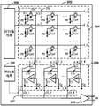
- FIG. 2 is a circuit structure diagram of an embodiment of at least one fingerprint sensor among the plurality of fingerprint sensors shown in FIG. 1.
- FIG. 3 is a structural diagram of an embodiment of a part of the fingerprint sensing pixel shown in FIG. 2.
- FIG. 4 is a structural diagram of another embodiment of a part of the fingerprint sensing pixel shown in FIG. 2.
- FIG. 5 is a schematic diagram of an embodiment of multiple timing control signals generated by the control circuit shown in FIG. 1.
- FIG. 6 is a schematic diagram of an embodiment of signal timing involved in the circuit operation shown in FIG. 5.
- FIG. 7 is a flowchart of an embodiment of a fingerprint recognition method of the present disclosure.
- the fifth heavily-doped area is the fifth heavily doped area
- PX fingerprint sensor pixels
- PX fingerprint sensor
- DBS data bus, data bus, DBS, etc.
- AO1-AO4 AO
- analog sensor output AO, AO, AO, AO, AO
- FIG. 1 is a functional block diagram of an embodiment of a fingerprint identification device of the present disclosure.
- the fingerprint recognition device 100 may be implemented as at least a part of an electronic device with a fingerprint recognition function, such as a mobile phone, a lithographic computer, a notebook computer, a wearable device with a fingerprint recognition function, a portable computer with a fingerprint recognition function, or other fingerprints Identify at least a part of the functional electronic device.
- a fingerprint recognition function such as a mobile phone, a lithographic computer, a notebook computer, a wearable device with a fingerprint recognition function, a portable computer with a fingerprint recognition function, or other fingerprints Identify at least a part of the functional electronic device.
- the “fingerprint” referred to in this disclosure may represent fingerprints, palm prints, or other textures with biological characteristics.
- the following uses a fingerprint sensing device with four fingerprint sensors to illustrate the fingerprint recognition mechanism of the present disclosure, however, those skilled in the art should understand the fingerprint recognition mechanism of the present disclosure after reading the contents of the specification It can be applied to fingerprint recognition devices with M fingerprint sensors, where M is a positive integer.
- the fingerprint recognition device 100 includes (but is not limited to) a plurality of fingerprint sensors 102_1-102_4 and a control circuit 110, wherein each fingerprint sensor includes a pixel array (ie one of the plurality of pixel arrays 104_1-104_4), wherein the pixel array There are multiple fingerprint sensing pixels arranged in multiple rows and multiple columns (not shown in FIG. 1).
- multiple fingerprint sensors 102_1-102_4 may be disposed adjacent to each other in the fingerprint recognition device 100 to form a large-scale fingerprint sensing area DTA.
- multiple fingerprint sensors 102_1-102_4 may be disposed adjacent to each other on the display screen of the electronic device (FIG. 1 not shown) below to provide users with a large-scale under-screen fingerprint recognition area.
- multiple fingerprint sensors 102_1-102_4 can increase the area available for the user to input fingerprint information through a predetermined arrangement.
- a plurality of fingerprint sensors 102_1-102_4 may be arranged at intervals along a predetermined direction and staggered in a direction perpendicular to the predetermined direction, where the predetermined direction may be a row direction or a column direction.
- the range of the fingerprint sensing area DTA is greater than the sum of the corresponding sensing ranges of the multiple pixel arrays 104_1-104_4.
- the plurality of fingerprint sensors 102_1-102_4 may be arranged at intervals and arranged in a rectangular shape, so that the range of the fingerprint sensing area DTA is greater than the sum of the corresponding sensing ranges of the plurality of pixel arrays 104_1-104_4.
- a plurality of fingerprint sensors 102_1-102_4 may be arranged at intervals along the row direction, wherein the pixel array 104_1 and the pixel array 104_2 are separated by a predetermined distance Da, and the pixel array 104_2 and the pixel array 104_3 are separated by a predetermined distance Db, pixels The array 104_3 and the pixel array 104_4 are separated by a predetermined distance Dc.
- a plurality of fingerprint sensors 102_1-102_4 may be staggered in the column direction, wherein the lower boundary of the pixel array 104_2 and the lower boundary of the pixel array 104_1 are separated by a predetermined distance Dd in the column direction, and the upper boundary of the pixel array 104_2 and the pixel array
- the upper boundary of 104_1 is separated by a predetermined distance De in the column direction
- the lower boundary of pixel array 104_3 and the lower boundary of pixel array 104_2 are separated by a predetermined distance Df in the column direction
- the upper boundary of pixel array 104_4 and the upper boundary of pixel array 104_3 They are separated by a predetermined distance Dg in the column direction.
- the control circuit 110 is externally connected to the plurality of fingerprint sensors 102_1-102_4 as a shared/common timing control circuit for the plurality of fingerprint sensors 102_1-102_4.
- the control circuit 110 and each fingerprint sensor may be arranged on different chips to enable the pixel array of each of the N fingerprint sensors in the plurality of fingerprint sensors 102_1-102_4 in a frame period to be line-by-line Drive multiple rows of fingerprint sensing pixels in the pixel array of each of the plurality of fingerprint sensors 102_1-102_4, where N is a positive integer less than or equal to the number (ie, 4) of the plurality of fingerprint sensors 102_1-102_4. That is to say, the control circuit 110 can enable each pixel array of one or more fingerprint sensors within one frame period to drive the multiple rows of fingerprint sensing pixels in each pixel array of the enabled fingerprint sensors line by line.
- the control circuit 110 may perform time-sharing control on the activated multiple fingerprint sensors, thereby driving multiple rows of fingerprint sensing pixels in each pixel array. For example (but the disclosure is not limited to this), in a frame period, the control circuit 110 may alternately activate a row of fingerprint sensing pixels of each pixel array of the plurality of fingerprint sensors 102_1-102_4 to drive each pixel array row by row Multi-line fingerprint sensing pixels. In other words, the driving timing of each pixel array is determined by the external control circuit 110. In this way, each fingerprint sensor can eliminate the need for a timing generation circuit, expand the setting range of the pixel array, and increase the area available for the user to input fingerprint information.
- the control circuit 110 can provide N timing control signals to the enabled N fingerprint sensors, so that each fingerprint sensor in the enabled N fingerprint sensors can drive multiple rows of fingerprints in the corresponding pixel array according to the corresponding timing control signals Sensing pixels.
- the control circuit 110 may provide a plurality of timing control signals TS1-TS4 to the plurality of fingerprint sensors 102_1-102_4 to perform time-sharing control on the plurality of fingerprint sensors 102_1-102_4, thereby driving the plurality of fingerprint sensors 102_1-102_4 individually
- the pixel array has multiple rows of fingerprint sensing pixels.
- the following uses the control circuit 110 to enable multiple fingerprint sensors 102_1-102_4 within one frame period (that is, the number of enabled fingerprint sensors (ie, the aforementioned N) is equal to that of the fingerprint sensor provided in the fingerprint recognition device 100 Number) of the embodiments to illustrate the fingerprint recognition scheme of the present disclosure.
- the control circuit 110 enabling one or more fingerprint sensors within a frame period is within the scope of the present disclosure.
- control circuit 110 can also be used as a signal processing circuit shared/common by multiple fingerprint sensors 102_1-102_4 to further increase the setting range of the pixel array and the input area of fingerprint information.
- the enabled fingerprint sensor can collect fingerprint images and generate an analog sensor output (i.e., one of a plurality of analog sensor outputs AO1-AO4).
- the control circuit 110 may perform analog-to-digital conversion on the analog sensor output generated by each of the fingerprint sensors enabled in the plurality of fingerprint sensors 102_1-102_4, thereby identifying fingerprint information. Therefore, it is not necessary to provide an analog-to-digital conversion circuit for each fingerprint sensor.
- the control circuit 110 includes (but is not limited to) a timing generator 112, an analog-to-digital conversion circuit 114, and an image signal processing module 117.
- the timing generator 112 is used to generate a plurality of timing control signals TS1-TS4.
- Multiple fingerprint sensors 102_1-102_4 can be activated in turn according to multiple timing control signals TS1-TS4, driving one row of fingerprint sensing pixels of each pixel array at a time, thereby driving multiple rows of fingerprint sensing of each pixel array row by row Pixels.
- Each timing control signal may include at least one of a frame synchronization signal (or vertical synchronization signal), a horizontal synchronization signal, and a pixel clock signal.
- the analog-to-digital conversion circuit 114 is coupled to the plurality of fingerprint sensors 102_1-102_4, and is used to alternately convert the plurality of analog sensor outputs AO1-AO4 generated by the plurality of fingerprint sensors 102_1-102_4 into a digital sensor output DO.
- the analog-to-digital conversion circuit 114 can convert the analog sensor output AO1 to the digital sensor output DO; when the fingerprint sensor 102_2 is enabled, the analog-to-digital conversion circuit 114 can convert the analog sensor The output AO2 is converted to a digital sensor output DO; and so on.
- the analog sensor output generated by each fingerprint sensor is processed by an external control circuit 110, and each fingerprint sensor can eliminate the need for an analog-to-digital conversion circuit, thereby increasing the setting range of the pixel array and the input area of fingerprint information.
- the analog-to-digital conversion circuit 114 may include a multiplexer (MUX) 115 and an analog-to-digital converter (ADC) 116.
- the multiplexer 115 has a plurality of input terminals TI1-TI4 and an output terminal TO for selectively coupling the plurality of input terminals TI1-TI4 to the output terminal TO, wherein the plurality of input terminals TI1-TI4 are respectively used for receiving Multiple analog sensor outputs AO1-AO4.
- the multiplexer 115 may alternately input N of the multiple input terminals TI1-TI4
- the terminal is coupled to the output terminal TO to output a corresponding analog sensor output (that is, one of the N analog sensor outputs coupled to the N input terminals).
- the analog-to-digital converter 116 is coupled to the output terminal TO for receiving one of the N analog sensor outputs from the output terminal TO (for example, one of the multiple analog sensor outputs AO1-AO4), And converting the analog sensor output into a digital sensor output DO.
- the image signal processing module 117 is coupled to the analog-to-digital conversion circuit 114 for performing band-pass filtering processing on the digital sensor output DO (for example, performing band-pass filtering processing on the digital sensor output DO) to generate a fingerprint image signal IMG, For subsequent fingerprint recognition. Since the digital sensing output DO can indicate the pixel data of a row of fingerprint sensing pixels acquired by each fingerprint sensor, the image signal processing module 117 can obtain the fingerprint sensing area DTA within a frame period according to the digital sensing output DO Fingerprint images collected. For example (but not limited to this disclosure), the image signal processing module 117 may include a line buffer circuit (line) 118 and an image signal processor (ISP) 119.
- line line
- ISP image signal processor
- the line buffer circuit 118 is coupled to the analog-to-digital converter 116 for buffering pixel data of multiple lines of fingerprint sensing pixels (ie, the digital sensor output DO corresponding to each line driving operation).
- the line buffer circuit 118 may include a plurality of line buffers (not shown in FIG. 1), and each line buffer may buffer pixel data of one or more lines of fingerprint sensing pixels.
- the image signal processor 119 is coupled to the line buffer circuit 118 for performing band-pass filtering and/or image stitching on pixel data acquired by multiple fingerprint sensors 102_1-102_4 within a frame period to generate a fingerprint sensing area
- the fingerprint image ie, fingerprint image signal IMG
- DTA fingerprint image signal IMG
- the timing generator 112 can generate a plurality of timing control signals TS1-TS4 to activate a row of fingerprint sensing pixels of the plurality of pixel arrays 104_1-104_4 in a frame period, thereby driving each pixel array row by row Multi-line fingerprint sensing pixels.
- the multiple fingerprint sensors 102_1-102_4 can alternately output multiple analog sensor outputs AO1-AO4, where each analog sensor output includes pixel data of a row of fingerprint sensor pixels.
- Multiplexer 115 alternately provides multiple analog sensor outputs AO1-AO4 to analog-to-digital converter 116, so that analog-to-digital converter 116 can alternately output multiple analog sensor outputs AO1-AO4 corresponding digital sensor outputs (digital transmission Sense output DO) to the line buffer circuit 118.
- the image signal processor 119 can perform image stitching according to the data stored in the line buffer circuit 118 to generate the fingerprint image collected by the fingerprint sensing area DTA within one frame period.
- the fingerprint sensing scheme of the present disclosure can greatly increase the pixels
- the setting range of the array provides a large-scale fingerprint sensing area, thereby enhancing the user experience.
- the fingerprint sensing scheme of the present disclosure has a simplified fingerprint sensing pixel structure, which not only reduces the complexity of the production process, but also further improves the pixel array provided separately from the control circuit in the fingerprint sensor Of the proportion.
- FIG. 2 is a circuit structure diagram of an embodiment of at least one fingerprint sensor among the plurality of fingerprint sensors 102_1-102_4 shown in FIG. 1. That is to say, at least one of the plurality of fingerprint sensors 102_1-102_4 shown in FIG. 1 can be implemented by the fingerprint sensor 202, wherein the fingerprint sensor 202 can be controlled according to the timing control signal TS (eg, the timing control shown in FIG. 1 One of the signals TS1-TS4) collects fingerprint images.
- TS timing control signal
- the fingerprint sensor 202 may include (but not limited to) a plurality of scanning lines R_1-R_H, a plurality of data lines C_1-C_W, a pixel array 204, a row of scanning circuits 205, an integrating circuit 206, a column of selection circuits 207, A column of scanning circuits 208 and a buffer circuit 209. Both H and W are positive integers greater than 1.
- the pixel array 204 includes a plurality of fingerprint sensing pixels PX arranged in H rows and W columns, wherein a plurality of scanning lines R_1-R_H are respectively provided corresponding to the plurality of rows of the pixel array 204, and a plurality of data lines C_1-C_W are respectively The multiple columns of the pixel array 204 are arranged correspondingly.
- each fingerprint sensing pixel PX includes a photodiode PD, a storage capacitor Cpd, and a transistor MP.
- the transistor MP has a control terminal TCN, a first connection terminal TC1 and a second connection terminal TC2.
- the control terminal TCN is connected to the scan line corresponding to the fingerprint sensing pixel PX (that is, one of the multiple scan lines R_1-R_H).
- the first connection terminal TC1 is connected to the photodiode PD, wherein the photodiode PD and the storage capacitor Cpd are connected in parallel between the first connection terminal TC1 and a reference voltage (eg, ground voltage).
- the second connection terminal TC2 is connected to the data line corresponding to the fingerprint sensing pixel PX (that is, one of the plurality of data lines C_1-C_W).
- the row scanning circuit 205 is coupled to the plurality of scanning lines R_1-R_H, and is used to drive the plurality of scanning lines R_1-R_H according to the timing control signal TS to enable the corresponding fingerprint sensing pixels.
- the integration circuit 206 is coupled to the plurality of data lines C_1-C_W, and is used to receive pixel data transmitted by each data line (that is, one of the plurality of pixel data D_1-D_W) and integrate the pixel data to generate integration Data (that is, one of the multiple points of data I_1-I_W).
- the integrating circuit 206 may include, but is not limited to, a plurality of integrators, where each integrator includes a capacitor Cp, a capacitor Cfb, an amplifier AMP, a switch Rst, and a capacitor Ci.
- the capacitor Cp can be used to store corresponding pixel data.
- the capacitance Cfb can be implemented by a variable capacitance.
- the amplifier AMP can store the corresponding integral data in the capacitor Ci.
- the column selection circuit 207 is coupled to the integration circuit 206 and the column scanning circuit 208 for selectively outputting multiple pieces of integrated data I_1-I_W to the buffer circuit 209.
- the column selection circuit 207 may include (but not limited to) a plurality of switches CS_1-CS_W.
- the column scanning circuit 208 can control the switching operation of each switch according to the timing control signal TS, and output the corresponding integral data to the buffer circuit 209.
- the buffer circuit 209 can use the stored multiple integral data I_1-I_W as the analog sensor output AO (for example, one of the multiple analog sensor outputs AO1-AO4 shown in FIG. 1).
- the column scanning circuit 208 can turn on multiple switches CS_1-CS_W one by one, and sequentially output multiple pieces of integral data I_1-I_W to the buffer circuit 209.
- the column scanning circuit 208 can turn on a part or all of the multiple switches CS_1-CS_W at a time.
- the fingerprint sensing pixels PX may be exposed for a period of time (that is, the photodiode PD converts the optical signal into an electrical signal), the transistor MP will be cut off, and the integrating circuit The corresponding switch Rst in 206 will be turned on.
- the line scanning circuit 205 drives a line of fingerprint sensing pixels including the fingerprint sensing pixels PX
- the transistor MP will be turned on
- the switch Rst will be turned off
- the charge accumulated in the first connection terminal TC1 will be transferred to the corresponding integration in the integration circuit 206 To charge the capacitor Ci.
- the buffer circuit 209 can output the corresponding integral data as part of the analog sensor output.
- each fingerprint sensing pixel PX may include only a single transistor (ie, transistor MP)
- the pixel The proportion of the array 204 in the fingerprint sensor 202 may be much larger than the proportion of the pixel array in the existing fingerprint sensor (about 60%).
- the source follower will result in a smaller linear range and poorer linearity. Since each fingerprint sensing pixel PX may include only a single transistor, the fingerprint sensor 202 may have a better linear range and linearity.
- FIG. 3 is a structural diagram of an embodiment of a part of the fingerprint sensing pixel PX shown in FIG. 2.
- the fingerprint sensing pixel PX includes (but is not limited to) a substrate 320 with a first conductivity type, a first heavily doped region 322_1 with a second conductivity type, and a second heavily doped region 322_2 with a second conductivity type , A third heavily doped region 322_3 with the second conductivity type, a fourth heavily doped region 322_4 with the second conductivity type, and a fifth heavily doped region 324 with the first conductivity type.
- the first conductivity type is P type
- the second conductivity type is N type.
- the first conductivity type may be N-type
- the second conductivity type may be P-type
- the fingerprint sensing pixel PX may further include multiple insulating layers 325_1 and 325_2, multiple gate electrode layers 326_1 and 326_2, multiple lightly doped drains (LDD) 327_1 and 327_2, and multiple shallow trench isolations (shallow trench isolation, STI) structure 328_1-328_3 and a wire structure 329.
- LDD lightly doped drains
- a part of the first heavily doped region 322_1, the second heavily doped region 322_2, the insulating layer 325_1, the gate electrode layer 326_1, and the substrate 320 may form a transistor MP.
- the other part of the first heavily doped region 323_1 and the substrate 320 may form a photodiode PD.
- the first heavily doped region 322_1 and the second heavily doped region 322_2 are formed separately on one side of the substrate 320, wherein the first heavily doped region 322_1 is coupled to the first connection terminal TC1, and the second The heavily doped region 322_2 is coupled to the second connection terminal TC2.
- An insulating layer 325_1 (for example, a gate oxide layer) is formed on the side of the substrate 320 to partially cover the first heavily doped region 322_1 and the second heavily doped region 322_2, wherein the insulating layer 325_1 is formed under the first conductivity type In the channel region CR1, two sides of the channel region CR1 are in contact with the first heavily doped region 322_1 and the second heavily doped region 322_2, respectively.
- the distance between the first heavily doped region 322_1 and the second heavily doped region 322_2 may be greater than a predetermined distance, therefore, even if the channel region CR1 is close to the first heavily doped region
- the gate electrode layer 326_1 (for example, a polysilicon gate) is formed on the insulating layer 325_1 and is coupled to the control terminal TCN.
- the length of the first heavily doped region 322_1 along the side of the substrate 320 can be greater than the length of the second heavily doped region 322_2 along the side of the substrate 320, so that the transistor MP and the photodiode PD can The first heavily doped region 322_1 is shared.
- the third heavily doped region 322_3, the fourth heavily doped region 322_4, the insulating layer 325_2, the gate electrode layer 326_2, the plurality of lightly doped drain regions 327_1 and 327_2, and the substrate 320 may form a switch Rst.
- the third heavily doped region 322_3 and the fourth heavily doped region 322_4 are separately formed on the side of the substrate 320.
- An insulating layer 325_2 (for example, a gate oxide layer) is formed on the side of the substrate 320 to partially cover the third heavily doped region 322_3 and the fourth heavily doped region 322_4.
- the gate electrode layer 326_2 (for example, a polysilicon gate) is formed on the insulating layer 325_2.
- a channel region CR2 having a first conductivity type is formed below the insulating layer 325_1, wherein the two sides of the channel region CR2 are in contact with a plurality of lightly doped drain regions 327_1 and 327_2, respectively.
- the length of the channel region CR2 may be smaller than the length of the channel region CR1, therefore, the lightly doped drain region 327_1 may be disposed between the third heavily doped region 322_3 and the channel region CR2, and lightly doped
- the impurity drain region 327_2 is disposed between the fourth heavily doped region 322_4 and the channel region CR2, reducing/avoiding hot carrier injection effects and gate oxide layer leakage problems.
- the fifth heavily doped region 324 is formed on the side of the substrate 320 and can be coupled to a reference voltage (eg, ground voltage GND).
- a plurality of shallow trench isolation structures 328_1-328_3 can be used to reduce leakage current and/or provide a larger breakdown voltage, wherein the shallow trench isolation structure 328_1 can be disposed on one side of the first heavily doped region 322_1, the shallow trench The isolation structure 328_2 may be disposed between the second heavily doped region 322_2 and the third heavily doped region 322_3, and the shallow trench isolation structure 328_3 may be disposed between the fourth heavily doped region 322_4 and the fifth heavily doped region 324 between.
- the wire structure 329 may be used to connect the second heavily doped region 322_2 and the third heavily doped region 322_3.
- the three-layer photomask can be used to define the insulating layer 325_1/325_2, the gate electrode layer 326_1/326_2, and the shallow trench isolation structure 328_1/328_2/328_3, and the two-layer photomask can be used to define Heavily doped regions of different conductivity types, use a layer of photomask to define resistance protection oxide, use a layer of photomask to define contacts, use three layers of photomask to define metal layers (such as the first layer of metal) Layer M1 and second metal layer M2) and via, and a layer of photomask to define pads.
- the three-layer photomask can be used to define the insulating layer 325_1/325_2, the gate electrode layer 326_1/326_2, and the shallow trench isolation structure 328_1/328_2/328_3, and the two-layer photomask can be used to define Heavily doped regions of different conductivity types, use a layer of photomask to define resistance protection oxide, use a layer of photomask to define contacts,
- the number of photomask layers (for example, 11 layers) required by the pixel structure of the present disclosure is about one-third of the number of photomask layers required by the existing pixel structure using 4 transistors, so the production process can be greatly simplified Complexity and reduce production costs.
- FIG. 4 is a structural diagram of another embodiment of a part of the fingerprint sensing pixel PX shown in FIG. 2.
- the structure shown in FIG. 4 is substantially the same as the structure shown in FIG. 3, and the main difference between the two is that the structure shown in FIG. 4 uses the well region 422 having the second conductivity type and the substrate 320 to form the photodiode PD.
- the well region 422 and the first heavily doped region 422_1 are formed on the same side of the substrate 320 and are in contact with the first heavily doped region 422_1, where the depth DW of the well region 422 extending from the side of the substrate 320 to the other side is greater than
- the first heavily doped region 422_1 extends from the side of the substrate 320 to the depth DN of the other side.
- the photodiode structure shown in FIG. 4 can detect a wider wavelength range.
- the structure shown in FIG. 4 may only require one more mask layer than the structure shown in FIG. 3 (used to define the well region 422). In other words, compared with the existing pixel structure using four transistors, the structure shown in FIG. 4 can greatly simplify the complexity of the production process and reduce production costs.
- FIG. 5 is a schematic diagram of an embodiment of a plurality of timing control signals TS1-TS4 generated by the control circuit 110 shown in FIG.
- the control circuit 110 may provide a shared frame synchronization signal VS to multiple fingerprint sensors 102_1-102_4, and respectively provide different multiple horizontal synchronization signals HS1-HS4 to multiple fingerprint sensors 102_1-102_4.
- Each fingerprint sensor can drive multiple lines of fingerprint sensing pixels according to the frame synchronization signal VS and the corresponding horizontal synchronization signal. That is, the shared frame synchronization signal VS and a horizontal synchronization signal can be used as at least a part (i.e., part or all) of a timing control signal.
- control circuit 110 can also provide a shared pixel clock signal PCLK to multiple fingerprint sensors 102_1-102_4, wherein each fingerprint sensor can output pixel data according to the pixel clock signal PCLK (for example, the row scanning circuit 205 and columns shown in FIG. 2
- the scanning circuit 208 can perform a scanning operation according to the pixel clock signal PCLK, so that the fingerprint sensor 202 outputs pixel data) to the common data bus DBS.
- the frame synchronization signal VS, the horizontal synchronization signal HS1 and the pixel clock signal PCLK can be used as at least a part of the timing control signal TS1; the frame synchronization signal VS, the horizontal synchronization signal HS2 and the pixel clock signal PCLK can be used as at least the timing control signal TS2 Part; and so on.
- the multiple horizontal synchronization signals HS1-HS4 may not overlap each other. However, the present disclosure is not limited to this.
- FIG. 5 is a schematic diagram of an embodiment of signal timing involved in the circuit operation shown in FIG. 5.
- the frame synchronization signal VS can be used to notify each fingerprint sensor that it is ready to be exposed, wherein each fingerprint sensor can be paused for a default period of time (default time period) before starting exposure, in which multiple fingerprint sensors 102_1-102_4
- the exposure time can be the same, but it corresponds to a different default length of time.
- each fingerprint sensor can output an analog sensor output according to the corresponding timing control signal.
- the fingerprint sensor 102_1 can expose TE1 for a period of time, and output analog sensor output AO1 for a period of TR1.
- the fingerprint sensor 102_4 may be exposed to TE4 for a period of time, and the analog sensor output AO4 may be output from TR4 for a period of time.
- multiple fingerprint sensors 102_1-102_4 are ready to start collecting data for one image frame according to the frame synchronization signal VS.
- the fingerprint sensor 102_1 drives a row of fingerprint sensing pixels R11 according to the horizontal synchronization signal HS1 to collect fingerprint images.
- the fingerprint sensor 102_2 drives a row of fingerprint sensing pixels R21 according to the horizontal synchronization signal HS2;
- the fingerprint sensor 102_3 drives a row of fingerprint sensing pixels R31 according to the horizontal synchronization signal HS3; at time t4,
- the fingerprint sensor 102_4 drives a row of fingerprint sensing pixels R41 according to the horizontal synchronization signal HS4.
- multiple fingerprint sensors 102_1-102_4 can alternately output their respective analog sensor outputs (that is, one of the multiple analog sensor outputs AO1-AO4) to the data bus DBS (time point) t1'-t4').
- the fingerprint sensor 102_1 drives another row of fingerprint sensing pixels R12 according to the horizontal synchronization signal HS1; at time t6, the fingerprint sensor 102_2 drives another row of fingerprint sensing pixels R22 according to the horizontal synchronization signal HS2; at time At t7, the fingerprint sensor 102_3 drives another row of fingerprint sensing pixels R32 according to the horizontal synchronization signal HS3; at time t8, the fingerprint sensor 102_4 drives another row of fingerprint sensing pixels R42 according to the horizontal synchronization signal HS4.
- multiple fingerprint sensors 102_1-102_4 can alternately output their respective analog sensor outputs (that is, one of the multiple analog sensor outputs AO1-AO4) to the data bus DBS (time point) t5'-t8').
- the control circuit 110 can drive multiple rows of fingerprint sensing pixels of each pixel array row by row within a frame period FP to collect an image The pixel data of the frame.
- control circuit 110 may provide multiple frame synchronization signals to multiple fingerprint sensors 102_1-102_4 (ie, the control circuit 110 may generate four frame synchronization signals), wherein the multiple One of the frame synchronization signals and the corresponding one of the horizontal synchronization signals can be used as one of the multiple timing control signals TS1-TS4.
- the fingerprint recognition mechanism of the present disclosure can be simply summarized as the flowchart shown in FIG. 7.
- 7 is a flowchart of an embodiment of a fingerprint recognition method of the present disclosure. If the results obtained are substantially the same, the steps need not be performed in the order shown in FIG. 7. For example, certain steps may be inserted therein.
- the fingerprint identification method shown in FIG. 7 is described below with the fingerprint identification device 100 shown in FIG. 1. However, it is also feasible to apply the control method shown in FIG. 7 to other fingerprint recognition devices having multiple fingerprint sensors.
- the fingerprint recognition method shown in FIG. 7 can be simply summarized as follows.
- Step 702 Activate the pixel array of each of the N fingerprint sensors in the M fingerprint sensors within one frame period to drive the multiple rows of fingerprint sensing pixels of each pixel array of the N fingerprint sensors row by row, where M Is a positive integer greater than 1, and N is a positive integer less than or equal to M.
- M a positive integer greater than 1
- N a positive integer less than or equal to M.
- Each of the N fingerprint sensors collects fingerprint images when activated to generate an analog sensor output.
- the control circuit 110 may alternately activate a plurality of pixel arrays 104_1-104_4 (ie, M equals 4 and N equals M) within a frame period to drive multiple rows of fingerprint sensing pixels in each pixel array row by row.
- Each fingerprint sensor can collect fingerprint images when activated to generate an analog sensor output (that is, one of the multiple analog sensor outputs AO1-AO4).
- Step 704 Generate a fingerprint image signal according to the N analog sensor outputs respectively generated by the N fingerprint sensors.
- the control circuit 110 may generate the fingerprint image signal IMG according to the multiple analog sensor outputs AO1-AO4 generated by the multiple fingerprint sensors 102_1-102_4, respectively.
- step 702 when N is greater than 1, a row of fingerprint sensing pixels of each pixel array of the N fingerprint sensors may be activated in turn to drive the pixels of the N fingerprint sensors row by row
- the array has multiple rows of fingerprint sensing pixels.
- the control circuit 110 may alternately activate a row of fingerprint sensing pixels of each pixel array of the plurality of fingerprint sensors 102_1-102_4 to drive the rows of fingerprint sensing pixels of the plurality of pixel arrays 104_1-104_4 row by row.
- a shared frame synchronization signal may be provided to the M fingerprint sensors, and different N horizontal synchronization signals may be respectively provided to the N fingerprint sensors, so that the A plurality of rows of fingerprint sensing pixels in each pixel array of the N fingerprint sensors are driven line by line within a frame period.
- the control circuit 110 may provide a shared frame synchronization signal (such as the frame synchronization signal VS shown in FIG. 6) to multiple fingerprint sensors 102_1-102_4, and respectively provide different multiple horizontal synchronization signals (such as shown in FIG. 6).
- a plurality of horizontal synchronization signals HS1-HS4 that do not overlap with each other are given to a plurality of fingerprint sensors 102_1-102_4 to alternately drive a plurality of rows of fingerprint sensing pixels in each pixel array within a frame period.
- N frame synchronization signals may be respectively provided to the N fingerprint sensors, and N horizontal synchronization signals may be respectively provided to the N fingerprint sensors, so that the A plurality of rows of fingerprint sensing pixels in each pixel array of the N fingerprint sensors are driven line by line within a frame period.
- step 704 when N is greater than 1, the N analog sensor outputs may be converted into a digital sensor output in turn, and the fingerprint image signal may be generated according to the digital sensor output.
- the control circuit 110 may alternately convert multiple analog sensor outputs AO1-AO4 into digital sensor outputs DO, and perform band-pass filtering processing based on the digital sensor outputs DO to generate fingerprint sensor areas DTA within a frame period.
- the collected fingerprint image signal IMG is used for subsequent fingerprint recognition. Since those skilled in the art can understand the details of each step in the fingerprint identification method shown in FIG. 7 after reading the relevant paragraphs of FIGS. 1 to 6, further description will not be repeated here.
Landscapes
- Engineering & Computer Science (AREA)
- Theoretical Computer Science (AREA)
- Data Mining & Analysis (AREA)
- Bioinformatics & Cheminformatics (AREA)
- Bioinformatics & Computational Biology (AREA)
- Computer Vision & Pattern Recognition (AREA)
- Life Sciences & Earth Sciences (AREA)
- Evolutionary Biology (AREA)
- Evolutionary Computation (AREA)
- Physics & Mathematics (AREA)
- General Engineering & Computer Science (AREA)
- General Physics & Mathematics (AREA)
- Artificial Intelligence (AREA)
- Image Input (AREA)
- Measurement Of The Respiration, Hearing Ability, Form, And Blood Characteristics Of Living Organisms (AREA)
Abstract
一种指纹识别装置(100)和指纹识别方法。所述指纹识别装置(100)包括M个指纹传感器(102_1-102_4)和控制电路(110)。各指纹传感器(102_1-102_4)包括像素阵列(104_1-104_4),所述像素阵列(104_1-104_4)具有排列为多行与多列的多个指纹传感像素,M是大于1的正整数。控制电路(110)外接于所述M个指纹传感器(102_1-102_4)并为所述M个指纹传感器(102_1-102_4)所共享。所述控制电路(110)用以于帧周期内,启用所述M个指纹传感器(102_1-102_4)中N个指纹传感器(102_1-102_4)各自的像素阵列(104_1-104_4),以逐行驱动所述N个指纹传感器(102_1-102_4)各自的像素阵列(104_1-104_4)所具有的多行指纹传感像素,N是小于或等于M的正整数。所述指纹识别装置(100)可提供大范围的指纹传感区域,并可提高各像素阵列(104_1-104_4)在相应的指纹传感器(102_1-102_4)的占比。
Description
本公开涉及指纹信号处理技术,尤其涉及一种包括多个指纹传感器的指纹识别装置及其相关的指纹识别方法。
通过屏下指纹(in-display fingerprint)技术,指纹传感电路可以直接集成在手机屏幕的下方,无需额外设置在手机屏幕以外的区域,从而提高空间的利用率。通常指纹传感器芯片是采用互补金属氧化物半导体图像传感器(complementary metal oxide semiconductor image sensor,CMOS image sensor,简称CIS)技术的主动式/有源式像素传感器(active pixel sensor,APS)结构。然而,现有像素结构是利用4个晶体管以进行图像传感操作,不仅增加生产工艺的复杂度,还降低了指纹传感像素阵列在指纹传感器的占比。也就是说,指纹传感器只能提供一个小范围的指纹传感区域。因此,当用户以指纹操作手机时(例如,进行指纹解锁),用户的眼睛必须注视手机屏幕,以确保手指的位置位在这个小范围的指纹传感区域内,造成使用上的不便。
因此,需要一种创新的指纹识别方案,其可提供大尺寸的指纹传感区域,提升用户体验。
发明内容
本公开的目的之一在于提供一种包括多个指纹传感器的指纹识别装置及其相关的指纹识别方法,来解决上述问题。
本公开的一实施例提供了一种指纹识别装置。所述指纹识别装置包括M个指纹传感器和控制电路。各指纹传感器包括像素阵列,所述像素阵列具有排列为多行与多列的多个指纹传感像素,M是大于1的正整数。控制电路外接于所述M个指纹传感器并为所述M个指纹传感器所共享。所述控制电路,用以于帧周期内,启用所述M个指纹传感器中N个指纹传感器各自的像素阵列,以逐行驱动所述N个指纹传感器各自的像素阵列所具有的多行指纹传感像素,其中N是小于或等于M的正整数。
本公开的一实施例提供了一种指纹识别方法。所述指纹识别方法包括以下步骤:于帧周期内,启用M个指纹传感器中N个指纹传感器各自的像素阵列,以逐行驱动所述N个指纹传感器各自的像素阵列所具有的多行指纹传感像素,其中M是大于1的正整数,N是小于或等于M的正整数,所述N个指纹传感器中各指纹传感器于启用时采集指纹图像以产生模拟传感输出;以及根据所述N个指纹传感器分别产生的N个模拟传感输出,产生指纹图像信号。
图1是本公开指纹识别装置的一实施例的功能方框示意图。
图2是图1所示的多个指纹传感器其中的至少一个指纹传感器的一实施例的电路结构图。
图3是图2所示的指纹传感像素的一部分的一实施例的结构图。
图4是图2所示的指纹传感像素的一部分的另一实施例的结构图。
图5是图1所示的控制电路所产生的多个时序控制信号的一实施例的示意图。
图6是图5所示的电路操作涉及的信号时序的一实施例的示意图。
图7是本公开的指纹识别方法的一实施例的流程图。
其中,附图标记说明如下:
100 指纹识别装置
102_1-102_4、202 指纹传感器
104_1-104_4、204 像素阵列
110 控制电路
112 时序产生器
114 模数转换电路
115 复用器
116 模数转换器
117 图像信号处理模块
118 行缓存电路
119 图像信号处理器
205 行扫描电路
206 积分电路
207 列选择电路
208 列扫描电路
209 缓存电路
320 基板
322_1、422_1 第一重掺杂区
322_2 第二重掺杂区
322_3 第三重掺杂区
322_4 第四重掺杂区
324 第五重掺杂区
325_1、325_2 绝缘层
326_1、326_2 栅极电极层
327_1、327_2 轻掺杂漏区
328_1、328_2、328_3 浅沟槽隔离结构
329 导线结构
422 阱区
702、704 步骤
R_1-R_H 扫描线
C_1-C_W 数据线
PX 指纹传感像素
PD 光电二极管
Cpd 储存电容
MP 晶体管
TCN 控制端
TC1 第一连接端
TC2 第二连接端
Cp、Cfb、Ci 电容
AMP 放大器
Rst、CS_1-CS_W 开关
DBS 数据总线
CR1、CR2 沟道区
GND 接地电压
DTA 指纹传感区域
Da、Db、Dc、De、Df、Dg 预定距离
IMG 指纹图像信号
TS1-TS4、TS 时序控制信号
AO1-AO4、AO 模拟传感输出
DO 数字传感输出
D_1-D_W 像素数据
I_1-I_W 积分数据
DN、DW 深度
PCLK 像素时钟信号
VS 帧同步信号
HS1-HS4 水平同步信号
R11-R42 一行指纹传感像素
TE1、TE4、TR1、TR4 一段时间
t0-t8、t1’-t8’ 时间点
FP 帧周期
在说明书及之前的权利要求书当中使用了某些词汇来指称特定的组件。本领域的技术人员应可理解,制造商可能会用不同的名词来称呼同样的组件。本说明书及之前的权利要求书并不以名称的差异来作为区分组件的方式,而是以组件在功能上的差异来作为区分的基准。在通篇说明书及之前的权利要求书当中所提及的“包含”为一开放式的用语,故应解释成“包含但不限定于”。此外,“耦接”一词在此包含任何直接和间接的电连接手段。因此,若文中描述一第一装置耦接于一第二装置,则代表所述第一装置可直接电连接于所述第二装置,或通过其它装置或连接手段间接地电连接到所述第二装置。
图1是本公开指纹识别装置的一实施例的功能方框示意图。指纹识别装置100可实施为具有指纹识别功能的电子设备的至少一部份,例如手机、平版电脑、笔记本电脑、具有指纹识别功能的可穿戴设备、具有指纹识别功能的便携式计算机,或其他具有指纹识别功能的电子设备的至少一部份。值得注意的是,本公开所称的“指纹”可表示指纹、掌纹或其他具有生物表征的部位的纹路。此外,为了方便说明,以下采用具有4个指纹传感器的指纹传感装置来说明本公开的指纹识别机制,然而,本领域的技术人员在阅读说明书的内容之后,应可理解本公开的指纹识别机制可应用于具有M个指纹传感器的指纹识别装置,其中M是正整数。
指纹识别装置100包括(但不限于)多个指纹传感器102_1-102_4以及一控制电路110,其中各指纹传感器包括一像素阵列(即多个像素阵列104_1-104_4其中的一个),其中所述像素阵列具有排列为多行与多列的多个指纹传感像素(图1未示出)。在此实施例中,多个指纹传感器102_1-102_4可以彼此相邻设置在指纹识 别装置100中,以形成大范围的指纹传感区域DTA。举例来说,在指纹识别装置100是具有屏下指纹识别功能的电子设备的一部份的实施例中,多个指纹传感器102_1-102_4可以彼此相邻设置在所述电子设备的显示屏(图1未示出)下方,以提供用户大范围的屏下指纹识别区域。此外,多个指纹传感器102_1-102_4可通过预定的布置方式,增加可供用户输入指纹信息的区域。例如,多个指纹传感器102_1-102_4可沿著一预定方向间隔地设置,并在垂直于所述预定方向上交错排列,其中所述预定方向可以是行方向或列方向。这样,指纹传感区域DTA的范围大于多个像素阵列104_1-104_4相应的传感范围的总和。又例如,多个指纹传感器102_1-102_4可间隔地设置,并呈矩形排列,使指纹传感区域DTA的范围大于多个像素阵列104_1-104_4相应的传感范围的总和。
在此实施例中,多个指纹传感器102_1-102_4可沿著行方向间隔地设置,其中像素阵列104_1与像素阵列104_2相距一预定距离Da,像素阵列104_2与像素阵列104_3相距一预定距离Db,像素阵列104_3与像素阵列104_4相距一预定距离Dc。此外,多个指纹传感器102_1-102_4可在列方向上交错排列,其中像素阵列104_2的下边界与像素阵列104_1的下边界在列方向上相距一预定距离Dd,像素阵列104_2的上边界与像素阵列104_1的上边界在列方向上相距一预定距离De,像素阵列104_3的下边界与像素阵列104_2的下边界在列方向上相距一预定距离Df,像素阵列104_4的上边界与像素阵列104_3的上边界在列方向上相距一预定距离Dg。
控制电路110外接于多个指纹传感器102_1-102_4,作为多个指纹传感器102_1-102_4共享/共同的时序控制电路。在此实施例中,控制电路110可与各指纹传感器设置在不同的芯片上,用以于一个帧周期内,启用多个指纹传感器102_1-102_4中N个指纹传感器各自的像素阵列,以逐行驱动多个指纹传感器102_1-102_4各自的像素阵列所具有的多行指纹传感像素,其中N是小于或等于多个指纹传感器102_1-102_4的个数(即,4)的正整数。也就是说,控制电路110可在一个帧周期内,启用一个或多个指纹传感器各自的 像素阵列,以逐行驱动所启用的指纹传感器各自的像素阵列所具有的多行指纹传感像素。
在控制电路110用以启用多个指纹传感器的情形下,控制电路110可对对所启用的多个指纹传感器进行分时控制,从而驱动各自的像素阵列所具有的多行指纹传感像素。举例来说(但本公开不限于此),在一个帧周期内,控制电路110可轮流启用多个指纹传感器102_1-102_4各自的像素阵列的一行指纹传感像素,以逐行驱动各像素阵列所具有的多行指纹传感像素。也就是说,各像素阵列的驱动时序均是由外接的控制电路110来决定。这样,各指纹传感器可无需设置时序产生电路,使像素阵列的设置范围扩大,增加可供用户输入指纹信息的区域。
控制电路110可提供N个时序控制信号给所启用的N个指纹传感器,使所启用的N个指纹传感器中各指纹传感器可根据相应的时序控制信号,驱动相应的像素阵列所具有的多行指纹传感像素。举例来说,控制电路110可提供多个时序控制信号TS1-TS4给多个指纹传感器102_1-102_4,以对多个指纹传感器102_1-102_4进行分时控制,从而驱动多个指纹传感器102_1-102_4各自的像素阵列所具有的多行指纹传感像素。
为了方便说明,以下以控制电路110于一个帧周期内启用多个指纹传感器102_1-102_4(即,所启用的指纹传感器的个数(即上述的N)等于设置指纹识别装置100具有的指纹传感器的个数)的实施方式来说明本公开的指纹识别方案。然而,本领域的技术人员在阅读本公开的说明书内容之后,应可了解控制电路110于一个帧周期内启用一个或多个指纹传感器的实施方式均属于本公开的范畴。
此外,在某些实施方式中,控制电路110还可作为多个指纹传感器102_1-102_4共享/共同的信号处理电路,进一步增加像素阵列的设置范围和指纹信息的输入区域。例如,当一指纹传感器启用时,所启用的指纹传感器可采集指纹图像,并产生一模拟传感输出(即 多个模拟传感输出AO1-AO4其中的一个)。控制电路110可对多个指纹传感器102_1-102_4中所启用的指纹传感器各自产生的模拟传感输出进行模拟数字转换,从而识别指纹信息。因此,各指纹传感器可无需设置模数转换电路。
在此实施例中,控制电路110包括(但不限于)一时序产生器112、一模数转换电路114及一图像信号处理模块117。时序产生器112用以产生多个时序控制信号TS1-TS4。多个指纹传感器102_1-102_4可分别根据多个时序控制信号TS1-TS4轮流启用,一次驱动各自的像素阵列的一行指纹传感像素,从而逐行驱动各自的像素阵列所具有的多行指纹传感像素。各时序控制信号可包括帧同步信号(或垂直同步信号)、水平同步信号与像素时钟信号其中的至少一个。相关的说明容后再叙。
模数转换电路114耦接于多个指纹传感器102_1-102_4,用以轮流将多个指纹传感器102_1-102_4分别产生的多个模拟传感输出AO1-AO4转换为一数字传感输出DO。在此实施例中,当指纹传感器102_1启用时,模数转换电路114可将模拟传感输出AO1转换为数字传感输出DO;当指纹传感器102_2启用时,模数转换电路114可将模拟传感输出AO2转换为数字传感输出DO;以此类推。通过外接的控制电路110来处理各指纹传感器产生的模拟传感输出,各指纹传感器可无需设置模数转换电路,从而增加像素阵列的设置范围和指纹信息的输入区域。
举例来说(但本公开不限于此),模数转换电路114可包括一复用器(multiplexer,MUX)115以及一模数转换器(analog-to-digital converter,ADC)116。复用器115具有多个输入端TI1-TI4和一个输出端TO,用以选择性地将多个输入端TI1-TI4耦接到输出端TO,其中多个输入端TI1-TI4分别用以接收多个模拟传感输出AO1-AO4。在多个指纹传感器102_1-102_4中的N个指纹传感器(N小于或等于4)轮流启用以采集指纹图像的情形下,复用器115可轮流将多个输入端TI1-TI4中的N个输入端耦接到输 出端TO,以输出相应的模拟传感输出(即,所述N个输入端耦接的N个模拟传感输出其中的一个)。模数转换器116耦接输出端TO,用以从输出端TO接收所述N个模拟传感输出其中的一个模拟传感输出(例如,多个模拟传感输出AO1-AO4其中的一个),以及将所述模拟传感输出转换为数字传感输出DO。
图像信号处理模块117耦接于模数转换电路114,用以根据数字传感输出DO进行带通滤波处理(例如,对数字传感输出DO进行带通滤波处理),产生一指纹图像信号IMG,供后续指纹识别使用。由于数字传感输出DO可指示出各指纹传感器所获取的一行指纹传感像素的像素数据,因此,图像信号处理模块117可根据数字传感输出DO,获得一个帧周期内指纹传感区域DTA所采集的指纹图像。举例来说(但本公开不限于此),图像信号处理模块117可包括一行缓存电路(line buffer circuit)118和一图像信号处理器(image signal processor,ISP)119。行缓存电路118耦接于模数转换器116,用以缓存多行指纹传感像素的像素数据(即各行驱动操作相对应的数字传感输出DO)。例如,行缓存电路118可包括多个行缓存器(line buffer)(图1未示出),各行缓存器可缓存一行或多行指纹传感像素的像素数据。图像信号处理器119耦接于行缓存电路118,用以将多个指纹传感器102_1-102_4于一个帧周期内所获取的像素数据进行带通滤波处理和/或图像拼接,以产生指纹传感区域DTA于一个帧周期内所采集的指纹图像(即指纹图像信号IMG),供后续指纹识别使用。
于指纹识别操作中,时序产生器112可产生多个时序控制信号TS1-TS4,以于一个帧周期内轮流启用多个像素阵列104_1-104_4的一行指纹传感像素,从而逐行驱动各像素阵列所具有的多行指纹传感像素。多个指纹传感器102_1-102_4可轮流输出多个模拟传感输出AO1-AO4,其中各模拟传感输出包括一行指纹传感像素的像素数据。复用器115轮流将多个模拟传感输出AO1-AO4提供给模数转换器116,使模数转换器116可轮流输出多个模拟传感输出AO1-AO4相应的数字传感输出(数字传感输出DO)至行缓存电路118。接下 来,图像信号处理器119可根据行缓存电路118所储存的数据进行图像拼接,产生指纹传感区域DTA于一个帧周期内所采集的指纹图像。
通过将指纹传感器与控制电路(例如包括模数转换器和图像信号处理器的控制电路)分开设置(例如分开设置在两个芯片)的分离式设计,本公开的指纹传感方案可大幅增加像素阵列的设置范围,提供大范围的指纹传感区域,从而提升用户体验。值得注意的是,在某些实施例中,本公开的指纹传感方案具有简化的指纹传感像素结构,不仅降低生产工艺的复杂度,更进一步提高与控制电路分开设置的像素阵列在指纹传感器的占比。
图2是图1所示的多个指纹传感器102_1-102_4其中的至少一个指纹传感器的一实施例的电路结构图。也就是说,图1所示的多个指纹传感器102_1-102_4其中的至少一个指纹传感器可由指纹传感器202来实施,其中指纹传感器202可根据时序控制信号TS(例如图1所示的多个时序控制信号TS1-TS4其中的一个)进行指纹图像采集。指纹传感器202可包括(但不限于)多条扫描线R_1-R_H、多条数据线C_1-C_W、一像素阵列204、一行扫描电路205、一积分电路(integrating circuit)206、一列选择电路207、一列扫描电路208以及一缓存电路209。H与W均为大于1的正整数。像素阵列204包括排列为H行与W列的多个指纹传感像素PX,其中多条扫描线R_1-R_H分别与像素阵列204的所述多行对应设置,多条数据线C_1-C_W分别与像素阵列204的所述多列对应设置。在此实施例中,各指纹传感像素PX包括一光电二极管PD、一储存电容Cpd以及一晶体管MP。晶体管MP具有一控制端TCN、一第一连接端TC1以及一第二连接端TC2。控制端TCN连接到指纹传感像素PX相对应的扫描线(即多条扫描线R_1-R_H的其中一条)。第一连接端TC1连接到光电二极管PD,其中光电二极管PD和储存电容Cpd并联于第一连接端TC1与一参考电压(例如接地电压)之间。第二连接端TC2连接到指纹传感像素PX相对应的数据线(即多条数据线C_1-C_W的其中一条)。
行扫描电路205耦接于多条扫描线R_1-R_H,用以根据时序控制信号TS驱动多条扫描线R_1-R_H,以启用相应的指纹传感像素。积分电路206耦接于多条数据线C_1-C_W,用以接收各数据线所传输的像素数据(即多笔像素数据D_1-D_W的其中一个),并对所述像素数据进行积分以产生积分数据(即多笔积分数据I_1-I_W的其中一个)。在此实施例中,积分电路206可包括(但不限于)多个积分器,其中各积分器包括一电容Cp、一电容Cfb、一放大器AMP、一开关Rst以及一电容Ci。电容Cp可用来储存相应的像素数据。电容Cfb可由可变电容来实施。通过开关Rst的切换操作,放大器AMP可将相应的积分数据储存在电容Ci。
列选择电路207耦接于积分电路206和列扫描电路208,用以选择性地将多笔积分数据I_1-I_W输出到缓存电路209。在此实施例中,列选择电路207可包括(但不限于)多个开关CS_1-CS_W。列扫描电路208可根据时序控制信号TS控制各开关的切换操作,将相应的积分数据输出到缓存电路209。缓存电路209可将所储存的多笔积分数据I_1-I_W作为模拟传感输出AO(例如图1所示的多个模拟传感输出AO1-AO4其中的一个)。例如,列扫描电路208可逐一开启多个开关CS_1-CS_W,依序将多笔积分数据I_1-I_W输出到缓存电路209。又例如,在缓存电路209可同时储存多笔积分数据的情形下,列扫描电路208可一次开启多个开关CS_1-CS_W的一部分或全部。
于采集指纹图像的操作中,在行扫描电路205驱动像素阵列204之前,指纹传感像素PX可曝光一段时间(即光电二极管PD将光信号转换为电信号),晶体管MP会切断,而积分电路206中相对应的开关Rst会开启。当行扫描电路205驱动包括指纹传感像素PX的一行指纹传感像素时,晶体管MP会导通,开关Rst会关闭,而第一连接端TC1累积的电荷会转移到积分电路206中相对应的积分器,以对电容Ci充电。当列选择电路207导通相对应的开关(多个开关CS_1-CS_W其中的一个)时,缓存电路209可将相应的积分数据输出,作为模拟传感输出的一部分。
相比于采用4个晶体管的像素结构的指纹传感器,由于指纹传感器202可无需设置时序产生器和模数转换器,且各指纹传感像素PX可以只包括单一个晶体管(即晶体管MP),像素阵列204在指纹传感器202的占比(例如90%)可远大于现有指纹传感器中像素阵列的占比(约60%)。再者,在采用4个晶体管的像素结构的指纹传感器中,源极跟随器会造成较小的线性范围和较差的线性度。由于各指纹传感像素PX可以只包括单一个晶体管,指纹传感器202可具有较佳的线性范围和线性度。
请连同图2参阅图3。图3是图2所示的指纹传感像素PX的一部分的一实施例的结构图。指纹传感像素PX包括(但不限于)具有第一导电类型的一基板320、具有第二导电类型的一第一重掺杂区322_1、具有第二导电类型的一第二重掺杂区322_2、具有第二导电类型的一第三重掺杂区322_3、具有第二导电类型的一第四重掺杂区322_4,以及具有第一导电类型的一第五重掺杂区324。在此实施例中,第一导电类型是P型,而第二导电类型是N型。然而,在某些实施例中,第一导电类型可以是N型,而第二导电类型可以是P型。指纹传感像素PX还可包括多个绝缘层325_1和325_2、多个栅极电极层326_1和326_2、多个轻掺杂漏区(lightly doped drain,LDD)327_1和327_2、多个浅沟槽隔离(shallow trench isolation,STI)结构328_1-328_3以及一导线结构329。
第一重掺杂区322_1的一部分、第二重掺杂区322_2、绝缘层325_1、栅极电极层326_1和基板320可形成晶体管MP。第一重掺杂区323_1的另一部分和基板320可形成光电二极管PD。在此实施例中,第一重掺杂区322_1及第二重掺杂区322_2分开形成在基板320的一侧,其中第一重掺杂区322_1耦接到第一连接端TC1,而第二重掺杂区322_2耦接到第二连接端TC2。绝缘层325_1(例如,栅氧化层)形成在基板320的所述侧,以部分覆盖第一重掺杂区322_1和第二重掺杂区322_2,其中绝缘层325_1的下方形成具有第一导电类型的沟道区CR1,沟道区CR1的两侧分别与第一重掺杂区322_1和第二重掺杂区322_2接触。举例来说,第一重掺杂区322_1与第 二重掺杂区322_2之间的距离(即沟道区CR1的长度)可大于一预定距离,因此,即使沟道区CR1靠近第一重掺杂区322_1/第二重掺杂区322_2的地方没有设置浅沟槽隔离,仍不会(或几乎不会)有热载流子注入效应(hot carrier inject)和栅氧化层漏电的问题。栅极电极层326_1(例如,多晶硅栅)形成在绝缘层325_1上,并耦接到控制端TCN。值得注意的是,第一重掺杂区322_1沿著基板320的所述侧的长度可大于第二重掺杂区322_2沿著基板320的所述侧的长度,使晶体管MP与光电二极管PD可共用第一重掺杂区322_1。
第三重掺杂区322_3、第四重掺杂区322_4、绝缘层325_2、栅极电极层326_2、多个轻掺杂漏区327_1和327_2以及基板320可形成开关Rst。第三重掺杂区322_3及第四重掺杂区322_4分开形成在基板320的所述侧。绝缘层325_2(例如,栅氧化层)形成在基板320的所述侧,以部分覆盖第三重掺杂区322_3及第四重掺杂区322_4。栅极电极层326_2(例如,多晶硅栅)形成在绝缘层325_2上。在此实施例中,绝缘层325_1的下方形成具有第一导电类型的沟道区CR2,其中沟道区CR2的两侧分别与多个轻掺杂漏区327_1和327_2接触。举例来说,沟道区CR2的长度可小于沟道区CR1的长度,因此,可将轻掺杂漏区327_1设置在第三重掺杂区322_3与沟道区CR2之间,以及将轻掺杂漏区327_2设置在第四重掺杂区322_4与沟道区CR2之间,减少/避免热载流子注入效应和栅氧化层漏电的问题。
此外,第五重掺杂区324形成在基板320的所述侧,并可耦接到一参考电压(例如接地电压GND)。多个浅沟槽隔离结构328_1-328_3可用来减少漏电流和/或提供较大的击穿电压,其中浅沟槽隔离结构328_1可设置在第一重掺杂区322_1的一侧,浅沟槽隔离结构328_2可设置在第二重掺杂区322_2与第三重掺杂区322_3之间,以及浅沟槽隔离结构328_3可设置在第四重掺杂区322_4与第五重掺杂区324之间。导线结构329可用来连接第二重掺杂区322_2与第三重掺杂区322_3。
相比于采用4个晶体管的像素结构的指纹传感器,图3所示的结构需要的光罩层数可大幅减少。举例来说(但本公开不限于此),可利用三层光罩定义绝缘层325_1/325_2、栅极电极层326_1/326_2以及浅沟槽隔离结构328_1/328_2/328_3、利用两层光罩定义不同导电类型的重掺杂区、利用一层光罩定义电阻保护氧化物(resist protection oxide)、利用一层光罩定义接点(contact)、利用三层光罩定义金属层(例如第一层金属层M1和第二层金属层M2)和通路(via),以及利用一层光罩定义接垫(pad)。也就是说,本公开的像素结构需要的光罩层数(例如,11层)大约是现有采用4个晶体管的像素结构需要的光罩层数的三分之一,故可大幅简化生产工艺的复杂度,并减少生产成本。
请连同图2参阅图4。图4是图2所示的指纹传感像素PX的一部分的另一实施例的结构图。图4所示的结构和图3所示的结构大致相同,两者之间主要的差别在于图4所示的结构是采用具有第二导电类型的阱区422与基板320形成光电二极管PD。阱区422和第一重掺杂区422_1形成在基板320的同一侧,并与第一重掺杂区422_1接触,其中阱区422从基板320的所述侧延伸到另一侧的深度DW大于第一重掺杂区422_1从基板320的所述侧延伸到所述另一侧的深度DN。相比于图3所示的光电二极管结构,图4所示的光电二极管结构可以侦测较宽的波长范围。图4所示的结构需要的光罩层数可以只比图3所示的结构多一层(用于定义阱区422)。也就是说,相比于现有采用4个晶体管的像素结构,图4所示的结构可大幅简化生产工艺的复杂度,并减少生产成本。
以下参考图5和图6说明本公开指纹传感方案的时序控制方式的一个实施方式。首先请参阅图5,图5是图1所示的控制电路110所产生的多个时序控制信号TS1-TS4的一实施例的示意图。在此实施例中,控制电路110可提供共享的帧同步信号VS给多个指纹传感器102_1-102_4,以及分别提供不同的多个水平同步信号HS1-HS4给多个指纹传感器102_1-102_4。各指纹传感器可根据帧同步信号VS和相对应的水平同步信号驱动多行指纹传感像素。也就是说,共 享的帧同步信号VS和一个水平同步信号可作为一个时序控制信号的至少一部分(即,一部分或全部)。
此外,控制电路110还可提供共享的像素时钟信号PCLK给多个指纹传感器102_1-102_4,其中各指纹传感器可根据像素时钟信号PCLK输出像素数据(例如,图2所示的行扫描电路205和列扫描电路208可根据像素时钟信号PCLK进行扫描操作,使指纹传感器202输出像素数据)至共用的数据总线DBS。也就是说,帧同步信号VS、水平同步信号HS1和像素时钟信号PCLK可作为时序控制信号TS1的至少一部分;帧同步信号VS、水平同步信号HS2和像素时钟信号PCLK可作为时序控制信号TS2的至少一部分;以此类推。多个水平同步信号HS1-HS4彼此可不相重叠。然而,本公开并不以此为限。
请连同图5参阅图6。图6是图5所示的电路操作涉及的信号时序的一实施例的示意图。于此实施例中,帧同步信号VS可用来通知各指纹传感器准备进行曝光,其中各指纹传感器可先停顿一段默认时间(default time period)之后,再开始进行曝光,其中多个指纹传感器102_1-102_4的曝光时间可相同,但对应于不同的默认时间长度。经过曝光时间之后,各指纹传感器可根据相应的时序控制信号输出模拟传感输出。以指纹传感器102_1为例,指纹传感器102_1可曝光一段时间TE1,并于一段时间TR1输出模拟传感输出AO1。相似地,指纹传感器102_4可曝光一段时间TE4,并于一段时间TR4输出模拟传感输出AO4。
在时间点t0,多个指纹传感器102_1-102_4根据帧同步信号VS准备开始采集一个图像帧的数据。在时间点t1,指纹传感器102_1根据水平同步信号HS1驱动一行指纹传感像素R11以采集指纹图像。相似地,在时间点t2,指纹传感器102_2根据水平同步信号HS2驱动一行指纹传感像素R21;在时间点t3,指纹传感器102_3根据水平同步信号HS3驱动一行指纹传感像素R31;在时间点t4,指纹传感器102_4根据水平同步信号HS4驱动一行指纹传感像素R41。经过一段时间(例如,积分时间)之后,多个指纹传感器102_1-102_4 可轮流将各自的模拟传感输出(即多个模拟传感输出AO1-AO4其中的一个)输出至数据总线DBS(时间点t1’-t4’)。
接下来,在时间点t5,指纹传感器102_1根据水平同步信号HS1驱动另一行指纹传感像素R12;在时间点t6,指纹传感器102_2根据水平同步信号HS2驱动另一行指纹传感像素R22;在时间点t7,指纹传感器102_3根据水平同步信号HS3驱动另一行指纹传感像素R32;在时间点t8,指纹传感器102_4根据水平同步信号HS4驱动另一行指纹传感像素R42。经过一段时间(例如,积分时间)之后,多个指纹传感器102_1-102_4可轮流将各自的模拟传感输出(即多个模拟传感输出AO1-AO4其中的一个)输出至数据总线DBS(时间点t5’-t8’)。通过轮流启用多个指纹传感器102_1-102_4各自的像素阵列的一行指纹传感像素,控制电路110可于一个帧周期FP内逐行驱动各像素阵列所具有的多行指纹传感像素,采集一个图像帧的像素数据。
以上所述仅供说明的目的而已,并非用来限制本公开。举例来说,在某些实施例中,控制电路110可分别提供多个的帧同步信号给多个指纹传感器102_1-102_4(即,控制电路110可产生4个帧同步信号),其中所述多个的帧同步信号其中的一个帧同步信号和相应的一个水平同步信号可作为多个时序控制信号TS1-TS4其中的一个时序控制信号。
本公开的指纹识别机制可简单归纳为图7所示的流程图。图7是本公开的指纹识别方法的一实施例的流程图。假若所得到的结果实质上大致相同,则步骤不一定要按照图7所示的顺序来进行。举例来说,某些步骤可安插于其中。为了方便说明,以下搭配图1所示的指纹识别装置100来说明图7所示的指纹识别方法。然而,将图7所示的控制方法应用于其他具有多个指纹传感器的指纹识别装置也是可行的。图7所示的指纹识别方法可简单归纳如下。
步骤702:于一个帧周期内,启用M个指纹传感器中N个指纹传感器各自的像素阵列,以逐行驱动所述N个指纹传 感器各自的像素阵列所具有的多行指纹传感像素,其中M是大于1的正整数,N是小于或等于M的正整数,所述N个指纹传感器中各指纹传感器于启用时采集指纹图像以产生一模拟传感输出。例如,控制电路110可于一个帧周期内轮流启用多个像素阵列104_1-104_4(即,M等于4,且N等于M),以逐行驱动各像素阵列所具有的多行指纹传感像素。各指纹传感器于启用时可采集指纹图像,以产生一模拟传感输出(即多个模拟传感输出AO1-AO4其中的一个)。
步骤704:根据所述N个指纹传感器分别产生的N个模拟传感输出,产生一指纹图像信号。例如,控制电路110可根据多个指纹传感器102_1-102_4分别产生的多个模拟传感输出AO1-AO4,产生指纹图像信号IMG。
在某些实施例中,于步骤702,当N大于1时,可轮流启用所述N个指纹传感器各自的像素阵列的一行指纹传感像素,以逐行驱动所述N个指纹传感器各自的像素阵列所具有的多行指纹传感像素。例如,控制电路110可轮流启用多个指纹传感器102_1-102_4各自的像素阵列的一行指纹传感像素,以逐行驱动多个像素阵列104_1-104_4所具有的多行指纹传感像素。
在某些实施例中,于步骤702,可将共享的帧同步信号提供给所述M个指纹传感器,以及将不同的N个水平同步信号分别提供给所述N个指纹传感器,以于所述帧周期内逐行驱动所述N个指纹传感器各自的像素阵列所具有的多行指纹传感像素。例如,控制电路110可提供共享的帧同步信号(例如图6所示的帧同步信号VS)给多个指纹传感器102_1-102_4,以及分别提供不同的多个水平同步信号(例如图6所示的彼此不相重叠的多个水平同步信号HS1-HS4)给多个指纹传感器102_1-102_4,以于一个帧周期内轮流驱动各像素阵列所具有的多行指纹传感像素。
此外,在某些实施例中,于步骤702,可N个帧同步信号分别 提供给所述N个指纹传感器,以及将N个水平同步信号分别提供给所述N个指纹传感器,以于所述帧周期内逐行驱动所述N个指纹传感器各自的像素阵列所具有的多行指纹传感像素。
于步骤704中,当N大于1时,可轮流将所述N个模拟传感输出转换为一数字传感输出,以及根据所述数字传感输出产生所述指纹图像信号。例如,控制电路110可轮流将多个模拟传感输出AO1-AO4转换为数字传感输出DO,并根据数字传感输出DO进行带通滤波处理,产生指纹传感区域DTA于一个帧周期内所采集的指纹图像信号IMG,供后续指纹识别使用。由于本领域的技术人员通过阅读图1到图6相关的段落说明之后,应可了解图7所示的指纹识别方法中每一步骤的细节,因此进一步的说明在此便不再赘述。
以上所述仅为本公开的实施例而已,并不用于限制本公开,对于本领域的技术人员来说,本公开可以有各种更改和变化。凡在本公开的精神和原则之内,所作的任何修改、等同替换、改进等,均应包含在本公开的保护范围之内。
Claims (20)
- 一种指纹识别装置,其特征在于,包括:M个指纹传感器,其中各指纹传感器包括像素阵列,所述像素阵列具有排列为多行与多列的多个指纹传感像素,M是大于1的正整数;以及控制电路,外接于所述M个指纹传感器并为所述M个指纹传感器所共享,所述控制电路用以于帧周期内,启用所述M个指纹传感器中N个指纹传感器各自的像素阵列,以逐行驱动所述N个指纹传感器各自的像素阵列所具有的多行指纹传感像素,其中N是小于或等于M的正整数。
- 如权利要求1所述的指纹识别装置,其特征在于,当N大于1时,所述控制电路用以在所述帧周期内,轮流启用所述N个指纹传感器各自的像素阵列的一行指纹传感像素。
- 如权利要求1所述的指纹识别装置,其特征在于,所述控制电路用以提供N个时序控制信号给所述N个指纹传感器;所述N个指纹传感器中各指纹传感器根据相应的时序控制信号,驱动相应的像素阵列所具有的多行指纹传感像素。
- 如权利要求3所述的指纹识别装置,其特征在于,所述控制电路用以提供共享的帧同步信号给所述N个指纹传感器,以及分别提供不同的N个水平同步信号给所述N个指纹传感器;所述共享的帧同步信号和所述N个水平同步信号其中的一个水平同步信号作为所述N个时序控制信号其中的一个时序控制信号。
- 如权利要求3所述的指纹识别装置,其特征在于,所述控制电路用以分别提供N个帧同步信号给所述N个指纹传感器,以及分 别提供N个水平同步信号给所述N个指纹传感器;所述N个帧同步信号其中的一个帧同步信号和相应的一个水平同步信号作为所述N个时序控制信号其中的一个时序控制信号。
- 如权利要求4或5所述的指纹识别装置,其特征在于,所述N个水平同步信号彼此不相重叠。
- 如权利要求1所述的指纹识别装置,其特征在于,所述N个指纹传感器中各指纹传感器于启用时采集指纹图像以产生模拟传感输出;所述控制电路包括:模数转换电路,耦接于所述M个指纹传感器,用以轮流将所述N个指纹传感器分别产生的N个模拟传感输出转换为数字传感输出;以及图像处理单元,耦接于所述模数转换电路,用以对所述数字传感输出进行带通滤波处理,产生指纹图像信号。
- 如权利要求7所述的指纹识别装置,其特征在于,所述模数转换电路包括:复用器,具有M个输入端和一个输出端,所述复用器用以轮流将所述M个输入端耦接到所述输出端,其中所述M个输入端中的N个输入端分别用以接收所述N个模拟传感输出;以及模数转换器,耦接于所述输出端,用以从所述输出端接收所述N个模拟传感输出其中的一个模拟传感输出,以及将所述模拟传感输出转换为所述数字传感输出。
- 如权利要求1所述的指纹识别装置,其特征在于,所述M个指纹 传感器沿著预定方向间隔地设置,并在垂直于所述预定方向上交错排列。
- 如权利要求9所述的指纹识别装置,其特征在于,所述预定方向是行方向。
- 如权利要求1所述的指纹识别装置,其特征在于,所述指纹传感器还包括:多条扫描线,分别与所述像素阵列的所述多行对应设置;以及多条数据线,分别与所述像素阵列的所述多列对应设置;所述多个指纹传感像素的各指纹传感像素包括:光电二极管;以及晶体管,具有控制端、第一连接端、第二连接端,所述控制端连接到所述指纹传感像素相对应的扫描线,所述第一连接端连接到所述光电二极管,所述第二连接端连接到所述指纹传感像素相对应的数据线。
- 如权利要求11所述的指纹识别装置,其特征在于,所述指纹传感像素包括:具有第一导电类型的基板;具有第二导电类型的第一重掺杂区及第二重掺杂区,分开形成在所述基板的一侧,所述第一重掺杂区耦接到所述第一连接端,所述第二重掺杂区耦接到所述第二连接端,所述第一重掺杂区沿著所述基板的所述侧的长度大于所述第二重掺杂区沿著所述基板的所述侧的长度;绝缘层,形成在所述基板的所述侧,以部分覆盖所述第一重掺 杂区和所述第二重掺杂区,其中所述绝缘层的下方形成具有所述第一导电类型的沟道区,所述沟道区的两侧分别与所述第一重掺杂区和所述第二重掺杂区接触;以及栅极电极层,形成在所述绝缘层上,所述栅极电极层耦接到所述控制端;其中所述栅极电极层、所述绝缘层、所述第一重掺杂区的一部分、所述第二重掺杂区和所述基板形成所述晶体管;所述第一重掺杂区的另一部分和所述基板形成所述光电二极管。
- 如权利要求11所述的指纹识别装置,其特征在于,所述指纹传感像素包括:具有第一导电类型的基板;具有第二导电类型的第一重掺杂区及第二重掺杂区,分开形成在所述基板的一侧,所述第一重掺杂区耦接到所述第一连接端,所述第二重掺杂区耦接到所述第二连接端;绝缘层,形成在所述基板的所述侧,以部分覆盖所述第一重掺杂区和所述第二重掺杂区,其中所述绝缘层的下方形成具有所述第一导电类型的沟道区,所述沟道区的两侧分别与所述第一重掺杂区和所述第二重掺杂区接触;栅极电极层,形成在所述绝缘层上,所述栅极电极层耦接到所述控制端;以及具有所述第二导电类型的阱区,形成在所述基板的所述侧并与所述第一重掺杂区接触,所述阱区从所述基板的所述侧延伸到另一侧的深度大于所述第一重掺杂区从所述基板的所述侧延伸到所述另一侧的深度;其中所述栅极电极层、所述绝缘层、所述第一重掺杂区、所述第二重掺杂区和所述基板形成所述晶体管;所述阱区和所述基 板形成所述光电二极管。
- 如权利要求12或13所述的指纹识别装置,其特征在于,所述第一导电类型是P型,所述第二导电类型是N型。
- 一种指纹识别方法,其特征在于,包括以下步骤:于帧周期内,启用M个指纹传感器中N个指纹传感器各自的像素阵列,以逐行驱动所述N个指纹传感器各自的像素阵列所具有的多行指纹传感像素,其中M是大于1的正整数,N是小于或等于M的正整数,所述N个指纹传感器中各指纹传感器于启用时采集指纹图像以产生模拟传感输出;以及根据所述N个指纹传感器分别产生的N个模拟传感输出,产生指纹图像信号。
- 如权利要求15所述的指纹识别方法,其特征在于,启用所述M个指纹传感器中所述N个指纹传感器各自的像素阵列的步骤包括:当N大于1时,轮流启用所述N个指纹传感器各自的像素阵列的一行指纹传感像素。
- 如权利要求15所述的指纹识别方法,其特征在于,启用所述M个指纹传感器中所述N个指纹传感器各自的像素阵列的步骤包括:提供共享的帧同步信号给所述N个指纹传感器,以及分别提供不同的N个水平同步信号给所述N个指纹传感器,以于所述帧周期内逐行驱动所述N个指纹传感器各自的像素阵列所 具有的多行指纹传感像素。
- 如权利要求15所述的指纹识别方法,其特征在于,启用所述M个指纹传感器中所述N个指纹传感器各自的像素阵列的步骤包括:分别提供N个帧同步信号给所述N个指纹传感器,以及分别提供N个水平同步信号给所述N个指纹传感器,以于所述帧周期内逐行驱动所述N个指纹传感器各自的像素阵列所具有的多行指纹传感像素。
- 如权利要求17或18所述的指纹识别方法,其特征在于,所述N个水平同步信号彼此不相重叠。
- 如权利要求15所述的指纹识别方法,其特征在于,根据所述N个指纹传感器分别产生的所述N个模拟传感输出产生所述指纹图像信号的步骤包括:当N大于1时,轮流将所述N个模拟传感输出转换为数字传感输出;以及根据所述数字传感输出产生所述指纹图像信号。
Priority Applications (2)
| Application Number | Priority Date | Filing Date | Title |
|---|---|---|---|
| CN201880003038.0A CN109891429B (zh) | 2018-12-26 | 2018-12-26 | 指纹识别装置和指纹识别方法 |
| PCT/CN2018/123743 WO2020132913A1 (zh) | 2018-12-26 | 2018-12-26 | 指纹识别装置和指纹识别方法 |
Applications Claiming Priority (1)
| Application Number | Priority Date | Filing Date | Title |
|---|---|---|---|
| PCT/CN2018/123743 WO2020132913A1 (zh) | 2018-12-26 | 2018-12-26 | 指纹识别装置和指纹识别方法 |
Publications (1)
| Publication Number | Publication Date |
|---|---|
| WO2020132913A1 true WO2020132913A1 (zh) | 2020-07-02 |
Family
ID=66926779
Family Applications (1)
| Application Number | Title | Priority Date | Filing Date |
|---|---|---|---|
| PCT/CN2018/123743 Ceased WO2020132913A1 (zh) | 2018-12-26 | 2018-12-26 | 指纹识别装置和指纹识别方法 |
Country Status (2)
| Country | Link |
|---|---|
| CN (1) | CN109891429B (zh) |
| WO (1) | WO2020132913A1 (zh) |
Cited By (1)
| Publication number | Priority date | Publication date | Assignee | Title |
|---|---|---|---|---|
| US11978277B2 (en) | 2021-07-23 | 2024-05-07 | Google Llc | Under-display fingerprint sensor timing control |
Families Citing this family (9)
| Publication number | Priority date | Publication date | Assignee | Title |
|---|---|---|---|---|
| KR20210101977A (ko) * | 2020-02-11 | 2021-08-19 | 삼성전자주식회사 | 지문 감지 장치 및 그 방법 |
| CN113723148B (zh) * | 2020-05-26 | 2025-07-29 | 北京小米移动软件有限公司 | 指纹检测模组、显示面板及电子设备 |
| CN112668425B (zh) * | 2020-12-18 | 2022-11-01 | 深圳市汇顶科技股份有限公司 | 指纹检测的方法、指纹传感器和电子设备 |
| KR102829744B1 (ko) | 2020-12-18 | 2025-07-03 | 선전 구딕스 테크놀로지 컴퍼니, 리미티드 | 지문 검출 방법, 지문 센서 및 전자 장치 |
| CN115132134A (zh) * | 2021-03-23 | 2022-09-30 | 上海和辉光电股份有限公司 | 像素电路及其驱动方法、显示面板和显示装置 |
| US11798309B2 (en) * | 2021-04-15 | 2023-10-24 | Novatek Microelectronics Corp. | Fingerprint identification method for panel, electronic device, and control circuit |
| CN115761824B (zh) * | 2022-11-18 | 2026-03-13 | 北京奕斯伟计算技术股份有限公司 | 指纹识别模组、指纹识别方法及装置 |
| CN116110085A (zh) * | 2023-01-06 | 2023-05-12 | 北京集创北方科技股份有限公司 | 电容感应单元驱动装置、电容式指纹驱动芯片及电子设备 |
| CN116110086A (zh) * | 2023-02-16 | 2023-05-12 | 广州国同芯微电子有限公司 | 一种指纹传感装置的控制方法和指纹传感装置 |
Citations (5)
| Publication number | Priority date | Publication date | Assignee | Title |
|---|---|---|---|---|
| CN104850292A (zh) * | 2015-06-01 | 2015-08-19 | 京东方科技集团股份有限公司 | 一种内嵌式触摸屏、其驱动方法及显示装置 |
| CN105678258A (zh) * | 2016-01-05 | 2016-06-15 | 京东方科技集团股份有限公司 | 一种指纹识别器件、其驱动方法、显示面板及显示装置 |
| US20170116452A1 (en) * | 2015-10-23 | 2017-04-27 | Shenzhen Huiding Technology Co., Ltd. | Capacitance detecting sensors and related devices and systems |
| CN107908034A (zh) * | 2017-12-05 | 2018-04-13 | 武汉天马微电子有限公司 | 一种阵列基板、触控显示面板和触控显示面板驱动方法 |
| CN108171183A (zh) * | 2018-01-02 | 2018-06-15 | 京东方科技集团股份有限公司 | 显示基板及其制作方法、显示装置和指纹识别方法 |
Family Cites Families (9)
| Publication number | Priority date | Publication date | Assignee | Title |
|---|---|---|---|---|
| CN103810479B (zh) * | 2014-02-28 | 2019-04-05 | 成都费恩格尔微电子技术有限公司 | 指纹采集系统及指纹信息采集方法 |
| KR101881682B1 (ko) * | 2014-10-13 | 2018-07-24 | 선전 구딕스 테크놀로지 컴퍼니, 리미티드 | 지문 인식용 센서 픽셀 회로 |
| CN105574472B (zh) * | 2014-10-14 | 2019-05-28 | 上海箩箕技术有限公司 | 面阵指纹传感器 |
| CN106980808B (zh) * | 2016-01-18 | 2023-11-28 | 江西指芯智能科技有限公司 | 一种指纹采集电路及指纹传感器 |
| CN106250888A (zh) * | 2016-09-19 | 2016-12-21 | 汕头超声显示器(二厂)有限公司 | 一种具有大面积识别区域的指纹识别感应器及其应用 |
| KR102747024B1 (ko) * | 2017-02-07 | 2024-12-30 | 삼성디스플레이 주식회사 | 표시 장치 |
| CN107103278A (zh) * | 2017-03-09 | 2017-08-29 | 江苏邦融微电子有限公司 | 一种节省指纹传感器面积的采集电路 |
| CN107820618B (zh) * | 2017-09-30 | 2022-05-17 | 深圳市汇顶科技股份有限公司 | 传感像素单元及光学指纹传感器 |
| CN108596096B (zh) * | 2018-04-24 | 2021-01-22 | 京东方科技集团股份有限公司 | 指纹识别装置、显示面板及其制作方法、显示装置 |
-
2018
- 2018-12-26 WO PCT/CN2018/123743 patent/WO2020132913A1/zh not_active Ceased
- 2018-12-26 CN CN201880003038.0A patent/CN109891429B/zh active Active
Patent Citations (5)
| Publication number | Priority date | Publication date | Assignee | Title |
|---|---|---|---|---|
| CN104850292A (zh) * | 2015-06-01 | 2015-08-19 | 京东方科技集团股份有限公司 | 一种内嵌式触摸屏、其驱动方法及显示装置 |
| US20170116452A1 (en) * | 2015-10-23 | 2017-04-27 | Shenzhen Huiding Technology Co., Ltd. | Capacitance detecting sensors and related devices and systems |
| CN105678258A (zh) * | 2016-01-05 | 2016-06-15 | 京东方科技集团股份有限公司 | 一种指纹识别器件、其驱动方法、显示面板及显示装置 |
| CN107908034A (zh) * | 2017-12-05 | 2018-04-13 | 武汉天马微电子有限公司 | 一种阵列基板、触控显示面板和触控显示面板驱动方法 |
| CN108171183A (zh) * | 2018-01-02 | 2018-06-15 | 京东方科技集团股份有限公司 | 显示基板及其制作方法、显示装置和指纹识别方法 |
Cited By (1)
| Publication number | Priority date | Publication date | Assignee | Title |
|---|---|---|---|---|
| US11978277B2 (en) | 2021-07-23 | 2024-05-07 | Google Llc | Under-display fingerprint sensor timing control |
Also Published As
| Publication number | Publication date |
|---|---|
| CN109891429B (zh) | 2023-05-26 |
| CN109891429A (zh) | 2019-06-14 |
Similar Documents
| Publication | Publication Date | Title |
|---|---|---|
| CN109891429B (zh) | 指纹识别装置和指纹识别方法 | |
| US11496716B2 (en) | Solid state imaging device and electronic apparatus | |
| CN110771155B (zh) | 固态摄像装置、固态摄像装置的驱动方法、以及电子设备 | |
| KR100858452B1 (ko) | Cmos 이미지 센서 | |
| US8836833B2 (en) | Solid-state imaging apparatus having pixels with plural semiconductor regions | |
| EP1343310B1 (en) | Correlated double sampling circuit and CMOS image sensor including the same | |
| CN103297715B (zh) | 固体摄像装置及电子设备 | |
| US9113103B2 (en) | Solid-state imaging apparatus and imaging system | |
| CN102316281B (zh) | 固态成像装置和成像系统 | |
| CN107919370B (zh) | 具有堆叠的成像晶圆和数字晶圆的图像传感器 | |
| US20130070141A1 (en) | Solid-state imaging device, method for driving solid-state imaging device, and electronic apparatus | |
| CN111656772B (zh) | 摄像装置和电子设备 | |
| JP2006270292A (ja) | 物理量分布検知装置並びに物理情報取得方法および物理情報取得装置 | |
| KR102268707B1 (ko) | 이미지 센서 | |
| US20090046187A1 (en) | Solid-state imaging device | |
| JP2018098772A (ja) | 撮像素子および電子機器 | |
| US10910430B2 (en) | Imaging device with opening parts for power and signal paths | |
| JP2023068696A (ja) | 撮像素子および電子機器 | |
| CN111652188A (zh) | Tft工艺制作的感光传感器、光学指纹传感器及电子设备 | |
| JP2011244246A (ja) | 固体撮像装置 | |
| JP2018046088A (ja) | 固体撮像装置及び電子機器 | |
| WO2024202669A1 (ja) | 半導体装置および光検出装置 | |
| WO2025205221A1 (ja) | 固体撮像素子および電子機器 | |
| US20230403483A1 (en) | Imaging element and imaging device | |
| JP2010056401A (ja) | 固体撮像装置及び撮像システム |
Legal Events
| Date | Code | Title | Description |
|---|---|---|---|
| 121 | Ep: the epo has been informed by wipo that ep was designated in this application |
Ref document number: 18944413 Country of ref document: EP Kind code of ref document: A1 |
|
| NENP | Non-entry into the national phase |
Ref country code: DE |
|
| 122 | Ep: pct application non-entry in european phase |
Ref document number: 18944413 Country of ref document: EP Kind code of ref document: A1 |