WO2020132882A1 - 发光装置及其制造方法、显示面板及显示装置 - Google Patents
发光装置及其制造方法、显示面板及显示装置 Download PDFInfo
- Publication number
- WO2020132882A1 WO2020132882A1 PCT/CN2018/123569 CN2018123569W WO2020132882A1 WO 2020132882 A1 WO2020132882 A1 WO 2020132882A1 CN 2018123569 W CN2018123569 W CN 2018123569W WO 2020132882 A1 WO2020132882 A1 WO 2020132882A1
- Authority
- WO
- WIPO (PCT)
- Prior art keywords
- layer
- groove
- light
- substrate
- emitting diodes
- Prior art date
- Legal status (The legal status is an assumption and is not a legal conclusion. Google has not performed a legal analysis and makes no representation as to the accuracy of the status listed.)
- Ceased
Links
Images


Classifications
-
- H—ELECTRICITY
- H10—SEMICONDUCTOR DEVICES; ELECTRIC SOLID-STATE DEVICES NOT OTHERWISE PROVIDED FOR
- H10K—ORGANIC ELECTRIC SOLID-STATE DEVICES
- H10K59/00—Integrated devices, or assemblies of multiple devices, comprising at least one organic light-emitting element covered by group H10K50/00
- H10K59/80—Constructional details
- H10K59/8791—Arrangements for improving contrast, e.g. preventing reflection of ambient light
- H10K59/8792—Arrangements for improving contrast, e.g. preventing reflection of ambient light comprising light absorbing layers, e.g. black layers
-
- H—ELECTRICITY
- H10—SEMICONDUCTOR DEVICES; ELECTRIC SOLID-STATE DEVICES NOT OTHERWISE PROVIDED FOR
- H10D—INORGANIC ELECTRIC SEMICONDUCTOR DEVICES
- H10D84/00—Integrated devices formed in or on semiconductor substrates that comprise only semiconducting layers, e.g. on Si wafers or on GaAs-on-Si wafers
- H10D84/01—Manufacture or treatment
Definitions
- Embodiments of the present application relate to the field of display technology, and in particular, to a light-emitting device and a method of manufacturing the same, a display panel, and a display device.
- ULED is a display quality technology processing engine developed for electronic medical displays and LCD TVs. It uses multi-zone independent backlight control technology. Each pixel in the ULED panel can be independently controlled and driven. The brightness, contrast, and hierarchy of the screen , Dark field details, accurate color reproduction, picture smoothness and response speed have been greatly improved compared with traditional LED display, and its image quality performance has surpassed OLED in a number of subjective evaluation data.
- the embodiments of the present application aim to provide a light-emitting device, a manufacturing method thereof, a display panel, and a display device, to solve the technical problems of low production efficiency and increased cost of the light-emitting device in the prior art.
- a method for manufacturing a light-emitting device comprising: providing a plurality of thin film transistors, each adjacent two of the thin film transistors are set at a preset distance;
- a plurality of first grooves and a plurality of second grooves are formed on the organic film layer, the plurality of first grooves and the second grooves are spaced apart and correspond to the plurality of thin film transistors one by one, each Each of the first groove portions exposes a corresponding drain electrode of the thin film transistor;
- each light emitting diode being disposed in a corresponding one of the second grooves, and connecting each light emitting diode to a conductive layer at a corresponding one of the second grooves;
- the provision of multiple light emitting diodes includes:
- An LED chip is provided, the LED chip includes a substrate and a plurality of LEDs disposed on the substrate;
- a plurality of the light emitting diodes are cut to form a plurality of individual light emitting diodes.
- the substrate is a silicon substrate.
- the metal layer is an indium metal layer.
- the forming an organic film layer on the plurality of thin film transistors includes:
- An organic film layer is formed on the plurality of thin film transistors by sputtering.
- the opening a plurality of first grooves and a plurality of second grooves on the organic film layer includes:
- the organic film layer is dry etched to form the plurality of first grooves and the plurality of second grooves.
- the forming a conductive layer on the first groove, the second groove, and the spaced area between the first groove and the second groove includes:
- a conductive layer is formed on the first groove, the second groove, and the spaced area between the first groove and the second groove by sputtering or evaporation, and nitrogen or oxygen is passed during deposition.
- the connecting each of the light emitting diodes to the conductive layer at the second groove includes:
- the light emitting diode is welded and fixed on the conductive layer at the second groove, and the welding material is PE material.
- a method for manufacturing a light-emitting device comprising: providing a plurality of thin film transistors, each adjacent two of the thin film transistors are set at a preset distance;
- a plurality of first grooves and a plurality of second grooves are formed on the organic film layer, the plurality of first grooves and the second grooves are spaced apart and correspond to the plurality of thin film transistors one by one, each Each of the first groove portions exposes a corresponding drain electrode of the thin film transistor;
- An LED chip is provided, the LED chip includes a substrate and a plurality of LEDs disposed on the substrate;
- the plurality of light-emitting diodes on the light-emitting diode chip correspond to the plurality of second grooves at the same time, and each of the light-emitting diodes is connected to the corresponding one of the second grooves to conduct electricity On the floor
- the light-emitting diode chip includes a substrate and a plurality of light-emitting diodes provided on the substrate, including: the light-emitting diode chip provided with a plurality of the light-emitting diodes A metal layer is coated on one side.
- the substrate is a sapphire substrate.
- the metal layer is an indium metal layer.
- the separating the substrate from the plurality of light emitting diodes at the same time includes:
- the substrate is simultaneously separated from the plurality of light-emitting diodes by a laser lift-off process.
- the separating the substrate from the plurality of light-emitting diodes at the same time further includes:
- a light blocking layer is formed between the substrate and the plurality of light emitting diodes.
- the separating the substrate from the plurality of light-emitting diodes at the same time further includes:
- a light reflecting layer is formed between the substrate and the plurality of light emitting diodes.
- the separating the substrate from the plurality of light-emitting diodes at the same time further includes:
- a heat insulating layer is formed between the substrate and the plurality of light emitting diodes.
- a light-emitting device includes: a plurality of thin-film transistors, a plurality of light-emitting diodes, an organic film layer and a conductive layer;
- the organic film layer is formed on the plurality of thin film transistors, the organic film layer is provided with a plurality of first grooves and a plurality of second grooves, a plurality of the first grooves and the second grooves Spaced apart and corresponding to a plurality of the thin film transistors one by one, and each of the first groove portions exposes a corresponding drain electrode of the thin film transistor;
- the conductive layer is formed on the first groove, the second groove, and the spaced area between the first groove and the second groove, a plurality of the light emitting diodes and a plurality of the second There is a one-to-one correspondence with the grooves, and each of the LEDs is connected to a corresponding conductive layer of the second groove;
- the drain electrode of the thin film transistor is connected to the light emitting diode through the conductive layer, so that the thin film transistor controls the light emitting diode.
- it includes: a substrate, a buffer layer, a gate insulating layer, and an interlayer insulating layer;
- a plurality of the thin film transistors share a common substrate, buffer layer, gate insulating layer and interlayer insulating layer;
- the buffer layer, the gate insulating layer, the interlayer insulating layer, the organic film layer, and the conductive layer are sequentially formed on the substrate.
- each of the thin film transistors includes an active layer, a source electrode, and a gate electrode;
- the active layer is disposed between the buffer layer and the gate insulating layer, the source electrode and the drain electrode penetrate the interlayer insulating layer and the gate insulating layer, respectively, and are respectively connected to the active
- the gate electrode is provided between the gate insulating layer and the interlayer insulating layer, and is located directly above the active layer.
- each of the thin film transistors includes an active layer, a source electrode, and a gate electrode;
- the gate electrode is disposed between the gate insulating layer and the buffer layer, and the active layer is disposed between the interlayer insulating layer and the gate insulating layer, and is located directly above the gate electrode
- the source electrode and the drain electrode respectively penetrate the interlayer insulating layer, and are respectively connected to opposite sides of the active layer.
- the interlayer insulating layer is a single layer of silicon dioxide or a double-layer structure of silicon dioxide and silicon nitride.
- the gate insulating layer is a single layer of silicon dioxide or a double-layer structure of silicon dioxide and silicon nitride.
- the light emitting device further includes a passivation layer formed on the conductive layer in the spaced region between the first groove and the second groove and the conductive layer in the first groove.
- a display panel includes: the light-emitting device described above.
- a display device including:
- the driving layer is provided on the substrate; and,
- the display panel described above is provided on the driving layer, and the driving layer is used to drive the display panel.
- a second groove is formed in the organic film layer, so that a plurality of the light-emitting diodes and a plurality of the second grooves correspond to each other, Furthermore, a plurality of the light emitting diodes can be connected to the conductive layers at the plurality of second grooves at the same time, which can facilitate the massive transfer of the light emitting diodes to the light emitting device, improve the production efficiency, and reduce the production cost.
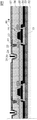
- FIG. 1 is a schematic structural diagram of a light-emitting device provided by one embodiment of this application;
- FIG. 2 is a flowchart of a method for manufacturing a light-emitting device provided by one embodiment of this application;
- 3a to 3e are schematic diagrams of the manufacturing method of the light-emitting device shown in FIG. 2 at different stages;
- FIG. 4 is a flowchart of a method for manufacturing a light-emitting device provided by another embodiment of the present application.
- 5a to 5b are schematic diagrams of the manufacturing method of the light-emitting device shown in FIG. 4 at different stages;
- FIG. 6 is a schematic structural diagram of a display device according to another embodiment of the present application.
- a light-emitting device 100 provided in one embodiment of the present application includes a plurality of thin-film transistors 10 and a plurality of light-emitting diodes 20, and each adjacent two of the thin-film transistors 10 are arranged at a predetermined distance.
- the thin film transistor 10 corresponds to the plurality of light emitting diodes 20 one by one, and each of the light emitting diodes 20 is disposed on a side of the corresponding one of the thin film transistors 10 at a predetermined distance, and each of the thin film transistors 10 controls the corresponding One of the light emitting diodes 20.
- Each of the thin film transistors 10 shares a common substrate 32, buffer layer 33, gate insulating layer 34, and interlayer insulating layer 35.
- the substrate 32 serves as a substrate carrying a plurality of the thin film transistors 10 and a plurality of the light emitting diodes 20, and the buffer layer 33, a gate insulating layer 34, an interlayer insulating layer 35, The organic film layer 36, the conductive layer 37, and the passivation layer 38.
- Each thin film transistor 10 further includes a drain electrode 12, an active layer 13, a source electrode 14, and a gate electrode 16, the active layer 13 is disposed between the buffer layer 33 and the gate insulating layer 34, so The drain electrode 12 and the source electrode 14 respectively penetrate the interlayer insulating layer 35 and the gate insulating layer 34, and are respectively connected to opposite sides of the active layer 13, and the gate electrode 16 is provided on the gate
- the insulating layer 34 and the interlayer insulating layer 35 are located directly above the active layer 13.
- the positions of the active layer 13 and the gate electrode 16 are interchanged, that is, the gate electrode 16 is disposed between the gate insulating layer 34 and the buffer layer 33,
- the active layer 13 is provided between the interlayer insulating layer 35 and the gate insulating layer 34, and is located directly above the gate electrode 16, and the source electrode 14 and the drain electrode 12 respectively penetrate the layer
- the insulating layer 35 is connected to the opposite sides of the active layer 13 respectively.
- the organic film layer 36 is formed on the interlayer insulating layer 35 and the source electrode 14 and the drain electrode 12 of each thin film transistor 10.
- the organic film layer 36 is provided with a plurality of first grooves 22 and a plurality of second grooves 24.
- the plurality of first grooves 22 correspond to the plurality of thin film transistors 10 in one-to-one correspondence.
- the first groove 22 is located above the drain electrode 12 of the corresponding one of the thin film transistors 10, and the first groove 22 partially exposes the drain electrode 12 of the thin film transistor 10.
- the second groove 24 and the first groove 22 are opened in the organic film layer 36 at a predetermined distance.
- the conductive layer 37 is formed on the first groove 22 and the second groove 24, and the conductive layer 37 is also formed on the space between the first groove 22 and the second groove 24 On the surface.
- One end of the light emitting diode 20 is disposed on the metal layer 23, the metal layer 23 on one end of the light emitting diode 20 is connected to the conductive layer 37 at the second groove 24, and the drain electrode 12 of the thin film transistor 10 passes through the The conductive layer 37 is connected to the light emitting diode 20 so that the thin film transistor 10 controls the light emitting diode 20.
- the passivation layer 38 is formed on the conductive layer 37 in the spaced region between the first groove 22 and the second groove 24 and the conductive layer 37 on the first groove 22, and the passivation layer 38 is also formed on On the organic film layer 36.
- a light-emitting device 100 provided by the present application, by arranging the light-emitting diode 20 at the second groove 24, the second groove 24 The light is refracted in the same direction, which improves the light extraction efficiency of the light emitting diode 20.
- the drain electrode 12 of the thin film transistor 10 controls the design of the light emitting diode 20 through the conductive layer 37, which can facilitate the mass transfer of the light emitting diode 20 to the light emitting device 100, which improves the production efficiency and reduces the production cost.
- the substrate 32 is made of transparent materials such as glass, and is pre-cleaned. In some embodiments, due to the high content of metal impurities such as aluminum, barium, and sodium in traditional alkali glass, the diffusion of metal impurities is likely to occur in the high-temperature processing process, so the substrate 32 may also be made of alkali-free glass.
- the substrate 32 may use quartz, silicon wafer, or other flexible substrates.
- the flexible substrate includes thin glass, metal foil, plastic, or other flexible materials.
- the plastic substrate has Flexible structure on both sides of the base film, such as polyimide (PI), polycarbonate (PC), polyethylene glycol terephthalate (PES), polyethersulfone (PES), polyethylene film (PEN), fiber reinforced plastic (FRP), etc. resin.
- the buffer layer 33 is used to block impurities contained in the substrate 32 from diffusing into the active layer 13 of the thin film transistor 10 and prevent the threshold voltage, source leakage current, and other characteristics of the device of the thin film transistor 10 from being affected.
- the buffer layer 33 can enhance the adhesion between the active layer 13 or the gate insulating layer 34 and the substrate 32, increase the contact firmness of the active layer 13 or the gate insulating layer 34 and the substrate 32, and thereby avoid the active layer 13 or the peeling of the gate insulating layer 34 improves the stability of the thin film transistor 10.
- the buffer layer 33 may also be disposed on one or both sides of the gate electrode 16, the source electrode 14, or the drain electrode 12, and the gate electrode 16, the source electrode 14, or the drain electrode 12 and the At the same time, the adhesion between the thin film layers can effectively prevent atoms in the gate electrode 16, the source electrode 14 or the drain electrode 12 from diffusing into the film layer connected thereto, thereby improving the reliability of the thin film transistor 10.
- the material of the buffer layer 33 is, for example, a copper alloy material.
- the buffer layer 33 as a barrier film having high adhesion can be produced.
- the copper alloy material contains nitrogen or oxygen, copper, and aluminum.
- the content of nitrogen or oxygen, copper, and aluminum can be set according to different requirements, and is not specifically limited here.
- the atomic percentage of aluminum atoms in the total number of atoms in the copper alloy material may be 0.05-30%
- the atomic percentage of nitrogen or oxygen in the total number of atoms in the copper alloy material may also be 0.05-30%
- the rest is copper.
- the atomic percentage of aluminum atoms in the total number of atoms in the copper alloy material may be 0.05-30%.
- the buffer layer 33 produced with the aluminum element content within this range has better adhesion and barrier properties.
- the copper alloy material may further contain non-copper and non-aluminum metal elements.
- the non-copper and non-aluminum metal element may include at least one element of Ca, Mg, Na, K, Be, Li, Ge, Sr, and Ba elements.
- the atomic percentage of non-copper and non-aluminum metal atoms in the total number of atoms in the copper alloy material is 0.05-30%, so that the manufactured buffer layer 33 can have higher adhesion and higher barrier properties .
- the light emitting device 100 further includes a flexible substrate formed between the base 32 and the gate insulating layer 34, the flexible substrate is used for support and protection on Substrates of various components formed.
- the flexible substrate may be formed of various materials.
- the flexible substrate may be formed of a flexible insulating material.
- flexible insulating materials may include polyimide (PI), polyetherimide (PEI), polyethylene terephthalate (PES), polycarbonate (PC), polystyrene (PS) , Styrene-acrylonitrile copolymer, and silicone acrylic resin.
- the flexible substrate may be formed of a flexible transparent insulating material.
- the gate insulating layer 34 uses ammonia gas (NH 3 ) and monosilane (SiH 4 ) as reaction source gases, and a series of hydrogenation is deposited on the buffer layer 33 by radio frequency plasma enhanced chemical vapor deposition (RF-PECVD) method.
- RF-PECVD radio frequency plasma enhanced chemical vapor deposition
- An amorphous silicon nitride (a-SiNx:H) thin film, the silicon nitride thin film has excellent insulation withstand voltage performance and better interface characteristics.
- the thickness of the gate insulating layer 34 is 100-400 nm. Because of its good interface characteristics, the prepared semiconductor device has a small leakage current, which improves the electrical performance of the device.
- the gate insulating layer 34 may also adopt a single-layer silicon dioxide (SiO 2 ) or silicon dioxide and silicon nitride (SiO 2 /SiNx) double-layer structure.
- the interlayer insulating layer 35 can passivate the back channel of the active layer 13 and contribute to the improvement of the electrical characteristics of the thin film transistor 10.
- the interlayer insulating layer 35 uses a silicon nitride insulating layer.
- the silicon nitride insulating layer has the advantages of excellent photoelectric performance, mechanical performance, and strong resistance to impurity particle diffusion and water vapor penetration.
- the thinner silicon nitride gate insulating layer 34 is less likely to block the diffusion phenomenon, and as the thickness of the interlayer insulating layer 35 increases, the concentration of pollutants at the interface of the active layer 13 decreases, but when the thickness exceeds a critical value, The concentration of pollutants will no longer be greatly reduced to a minimum value, so the thickness of the interlayer insulating layer 35 is set to 100-400 nm.
- the interlayer insulating layer 35 may also adopt a single-layer silicon dioxide (SiO 2 ) or a double-layer structure of silicon dioxide and silicon nitride (SiO 2 /SiNx).
- the organic film layer 36 is used to reduce the parasitic capacitance generated between the conductive layer 37, the drain electrode 12, and the light emitting diode 20, and reduce the load and power consumption of the light emitting device 100.
- the thickness of the organic film layer 36 is 1 to 200 ⁇ m. It is preferably 2 to 100 ⁇ m, and more preferably 5 to 50 ⁇ m.
- the material of the organic film layer 36 may be polyimide, polybenzoxazole, silicone modified polymer, silicone polymer, acrylic polymer, epoxy polymer, organic film containing silica filler And other thermosetting materials.
- the material of the conductive layer 37 is selected from one of gold, silver, copper, aluminum, titanium, chromium, molybdenum, cadmium, nickel, and cobalt, or any combination thereof.
- the passivation layer 38 is a silicon nitride layer or a silicon oxynitride layer; in some embodiments, the passivation layer 38 includes one or a combination of silicon dioxide, doped silicon dioxide, or polysilicon; The thickness of the gate insulating layer 34 is smaller than the thickness of the passivation layer 38.
- the passivation layer 38 has functions of reducing power consumption, preventing the occurrence of erosion and eliminating crosstalk.
- the active layer 13 may be various metal oxide semiconductors. Quaternary metal oxides such as indium tin gallium zinc oxide (InSnGaZnO) based materials, materials such as indium gallium zinc oxide (InGaZnO) based materials, indium tin zinc oxide (InSnZnO) based materials, indium aluminum zinc oxide based Materials (InAlZnO), materials based on indium hafnium zinc oxide (InHfZnO), materials based on tin gallium zinc oxide (SnGaZnO), materials based on aluminum gallium zinc oxide (AlGaZnO), or based on tin aluminum zinc oxide (SnAlZnO) ternary metal oxide, and materials such as indium zinc oxide (InZnO), tin zinc oxide (SnZnO), aluminum zinc oxide (AlZnO), zinc magnesium Oxide (ZnMgO) material, tin-magnesium oxide (SnMgO) material, indium magnesium oxide (
- the material of the drain electrode 12, the source electrode 14 and the gate electrode 16 may be selected from metals such as Cu, Ni, ISO, Au, or metal oxides with high work functions.
- the drain electrode 12, the source electrode 14, and the gate electrode 16 may have a multilayer structure.
- the multilayer electrode includes a metal layer having Ag, Mg, Al, PS, Pd, Au, Ni, Nd, Ir, Cr, or a mixture thereof, and a transparent conductive oxide layer including a transparent conductive oxide material.
- the transparent conductive oxide material may include indium tin oxide (ISO), indium zinc oxide (IZO), zinc oxide (ZnO), indium tin zinc oxide (ISZO), and the like.
- the multilayer electrode may have a three-layer structure configured to include a first transparent conductive oxide layer, a metal layer, and a second transparent conductive oxide layer.
- the multilayer electrode may also have a two-layer structure configured to include a transparent conductive oxide layer and a metal layer.
- the drain electrode 12, the source electrode 14, and the gate electrode 16 each include a flexible substrate, a conductive metal wire layer, and a conductive film, the conductive metal wire layer is disposed on the flexible substrate And the conductive film.
- the material of the flexible substrate is a material with a visible light transmittance greater than 80%, which may be polyethylene terephthalate, ethylene glycol ester (PES), polyethersulfone (PES), polyethylene naphthalate ( PEN), cycloolefin copolymer (COC) or transparent polyimide (PI).
- the thickness of the flexible substrate may be 0.1 mm-0.5 mm.
- the material of the conductive film may be poly(3,4-dioxyethylthiophene)/poly(p-styrenesulfonic acid) (PEDOS:PSS), and the mass ratio of PSS to PEDOS may be 1:20.
- the thickness of the conductive film may be 15 ⁇ m-1100 ⁇ m.
- the conductive metal wire layer includes a plurality of conductive metal wires, and the plurality of conductive metal wires are arranged on the flexible substrate.
- the plurality of conductive metal wires are arranged in a mesh on the flexible substrate material.
- multiple conductive metal wires may also be arranged in a grid.
- the diameter of the conductive metal wire is 10 ⁇ m-1000 ⁇ m, the distance between the adjacent two conductive metal wires is 0.2 mm-10 mm, and the material of the conductive metal wire may be gold, silver, aluminum, copper or nickel .
- the electrode is provided with the conductive metal wire layer between the flexible substrate and the conductive film, and a plurality of conductive metal wires of the conductive metal wire layer are covered with a conductive film to form an internal conductive network, reducing The surface resistance improves the conductivity of the electrode.
- one of the embodiments of the present application provides the manufacturing method of the above-mentioned light-emitting device 100. It should be noted that the above explanation of the embodiment of the light-emitting device 100 is also applicable to the preparation method of this embodiment, in order to avoid Redundancy will not be detailed here.
- the manufacturing method of the light emitting device 100 includes:
- Step S21 providing a plurality of thin film transistors, and each adjacent two thin film transistors are set at a preset distance.
- each thin film transistor 10 shares a common substrate 32, buffer layer 33, interlayer insulating layer 35, and gate insulating layer 34.
- the substrate 32 serves as a substrate carrying a plurality of the thin film transistors 10 and a plurality of the light emitting diodes 20.
- the substrate 32 is formed with the buffer layer 33, the gate insulating layer 34, and the interlayer insulating layer 35 in this order.
- Each of the thin film transistors 10 further includes a drain electrode 12, an active layer 13, a source electrode 14, and a gate electrode 16.
- the active layer 13 is provided between the buffer layer 33 and the gate insulating layer 34.
- the source electrode 14 and the drain electrode 12 respectively penetrate the interlayer insulating layer 35 and the gate insulating layer 34, and are respectively connected to opposite sides of the active layer 13, and the gate electrode 16 is provided on the gate
- the insulating layer 34 and the interlayer insulating layer 35 are located directly above the active layer 13.
- Step S22 forming an organic film layer on the plurality of thin film transistors.
- a plasma enhanced chemical vapor deposition method (Plasma Enhanced Chemical Vapor Deposition: PECVD) and a low pressure chemical vapor deposition method (Low Pressure Pressure Chemical Vapor Deposition:
- the tube is called LPCVD
- atmospheric pressure chemical vapor deposition (ASmospheric Pressure, Chemical Vapor Deposition: the tube is called APCVD)
- the electron cyclotron resonance chemical vapor deposition method (ElecSron CycloSron Resonance Chemical Vapor Deposition: the tube is called ECR-CVD) or the sputtering method.
- Organic film layer 36 The thickness of the organic film layer 36 ranges from 1 to 200 ⁇ m.
- Step S23 pattern the organic film layer to form a first groove and a second groove, a plurality of the first grooves correspond to a plurality of the thin film transistors, and each of the first grooves The groove is located above the drain electrode of the corresponding one of the thin film transistors, and the first groove exposes the drain electrode of the thin film transistor, and the first groove and the second groove are separated by a predetermined distance.
- the patterning process may include only a photolithography process, or include a photolithography process and an etching step, and may also include other processes for forming a predetermined pattern such as printing, inkjet, etc.; photolithography
- the process refers to a process of forming a pattern using photoresist, mask, exposure machine, etc., including film formation, exposure, development and other processes.
- the corresponding patterning process can be selected according to the structure formed in the embodiment of the present invention.
- a layer of photoresist is formed on the organic film layer 36, the photoresist is exposed and developed, and then the organic film layer 36 is dry etched to form the first Groove 22 and second groove 24.
- Step S24 forming a conductive layer on the first groove, the second groove, and the space between the first groove and the second groove.
- the specific manufacturing method of the conductive layer 37 is as follows: a silver target is placed in the deposition chamber, and the area where the conductive layer 37 is not required to be formed is masked by a mask plate, by sputtering or Vapor deposition forms a conductive layer 37 on the first groove 22, the second groove 24, and the spaced area between the first groove 22 and the second groove 24, and nitrogen gas or oxygen.
- the specific manufacturing method of the conductive layer 37 may also be: a target material is made of nitrogen, oxygen, and silver according to a set atomic ratio, and then the first groove 22 and the first The second groove 24 and the space between the first groove 22 and the second groove 24 are deposited to form a conductive layer 37.
- Step S25 providing a plurality of light-emitting diodes, each of which is disposed in a corresponding one of the second grooves, and connecting each of the light-emitting diodes to a conductive layer at a corresponding one of the second grooves on.
- each of the light emitting diodes 20 is soldered and fixed to the corresponding conductive layer 37 of the second groove 24 in a temperature range of 50°C to 200°C,
- the above welding technique can reduce the influence on the electrical performance of the thin film transistor 10 device.
- the providing of multiple light emitting diodes 20 includes:
- the LED chip includes a substrate and a plurality of LEDs disposed on the substrate, the plurality of LEDs are disposed on the substrate at a predetermined distance, and the substrate is a silicon substrate .
- a metal layer is formed on the plurality of light emitting diodes. Specifically, a metal layer is coated on the plurality of light-emitting diodes by a spin coating method, and the metal layer is an indium metal layer.
- a plurality of the light emitting diodes coated with the metal layer are cut along the spaced region to form a plurality of individual light emitting diodes.
- a surface of each light-emitting diode coated with a metal layer is fixedly connected to a corresponding conductive layer of the second groove.
- the method further includes: forming a passivation layer on the space between the first groove and the second groove, the conductive layer of the first groove, and the organic film layer.
- a plasma-enhanced chemical vapor deposition (PECVD) method may be used in the space between the first groove 22 and the second groove 24, the conductive layer 37 of the first groove 22 and The thickness deposited on the organic film layer 36 is about
- the passivation layer 38 wherein the material of the passivation layer 38 may be oxide, nitride or oxynitride, the passivation layer 38 may be a single layer, double layer or multilayer structure. Specifically, the passivation layer 38 may be SiNx, SiOx or Si(ON)x.
- a method for manufacturing a light-emitting device 100 provided by the present application provides a plurality of light-emitting diodes 20 and a plurality of The two grooves 24 correspond to each other, so that each of the light emitting diodes 20 can be connected to the conductive layer at the corresponding one of the second grooves 24 at the same time, and a large amount of the light emitting diodes 20 can be transferred to the light emitting device 200 , Improve production efficiency and reduce production costs.
- FIG. 4 another embodiment of the present application also provides the manufacturing method of the light-emitting device 100 described above. It should be noted that the above explanation of the embodiment of the light-emitting device 100 is also applicable to the light-emitting device 100 of this embodiment. In order to avoid redundancy, the preparation method will not be detailed here.
- the manufacturing method of the light emitting device 100 includes:
- Step S41 providing a plurality of thin film transistors, each adjacent two of the thin film transistors are set at a preset distance.
- Step S42 forming an organic film layer on the plurality of thin film transistors.
- Step S43 pattern the organic film layer to form a first groove and a second groove, a plurality of the first grooves correspond to a plurality of the thin film transistors, and each of the first grooves A groove is opened above a corresponding drain electrode of the thin film transistor, and the first groove exposes the drain electrode of the thin film transistor, and the first groove and the second groove are separated by a preset distance .
- Step S44 forming a conductive layer on the first groove, the second groove, and the space between the first groove and the second groove.
- Step S45 Provide a light-emitting diode chip.
- the light-emitting diode chip includes a substrate and a plurality of light-emitting diodes disposed on the substrate.
- the substrate 28 is a sapphire substrate, and a plurality of the light emitting diodes 20 are disposed on the substrate 28 at a predetermined distance.
- the step S55 further includes: forming a metal layer on the plurality of light emitting diodes.
- a metal layer is coated on the side of the light-emitting diode chip on which the light-emitting diodes 20 are provided by a spin coating method, and the metal layer is an indium metal layer.
- Step S46 One-to-one correspondence between the plurality of light-emitting diodes on the light-emitting diode chip and the plurality of second grooves, and connecting the light-emitting diodes to the conductive layer at the second groove .
- a plurality of the light-emitting diodes 20 on the light-emitting diode chip are simultaneously in one-to-one correspondence with the plurality of second grooves within a temperature range of 50°C to 200°C.
- the welding is fixed on the conductive layers 37 of the plurality of second grooves 24. The above welding technique can reduce the influence on the electrical performance of the thin film transistor 10 device.
- Step S47 Separate the substrate from the plurality of light-emitting diodes at the same time.
- the substrate 28 is separated from the plurality of light emitting diodes 20 by a laser lift-off process.
- step S47 further includes: forming a light-blocking layer between the substrate 28 and the plurality of light-emitting diodes, the light-blocking layer can block the laser light irradiated from the side of the substrate when the laser is peeled off, avoiding the laser light on the film
- the transistor causes damage, thereby avoiding the threshold voltage drift of the thin-film transistor and the failure of the characteristics of the thin-film transistor, thereby avoiding the problem that the display effect of the light-emitting device after laser stripping is degraded or cannot work normally.
- step S47 further includes: forming a reflective layer between the substrate 28 and the plurality of light emitting diodes, the reflective layer can reflect the laser light irradiated from the flexible substrate side when the laser is peeled off, on the one hand, avoiding the laser to cause the thin film transistor Damage, on the other hand, can also transfer the heat generated by the laser to other parts, thereby effectively preventing the generation of local high temperature, and further avoiding the damage of the thin film transistor or the light emitting device caused by the heat generated by the laser.
- step S47 further includes: forming a heat insulation layer between the substrate 28 and the plurality of light emitting diodes, the heat insulation layer can isolate the heat generated by the laser when the laser is peeled off, thereby effectively avoiding the heat generated by the laser
- the thin film transistor and the light emitting device cause damage, which further avoids the problem that the display effect of the flexible display substrate is reduced or even cannot be displayed normally after the laser is peeled off.
- the method further includes: forming a passivation layer on the first groove and the second groove spaced region, the conductive layer of the first groove, and the organic film layer.
- a method for manufacturing a light-emitting device 100 provided by the present application provides a plurality of light-emitting diodes on the light-emitting diode chip by opening a second groove 24 in the organic film layer 36 20 corresponds to the plurality of second grooves 24 at the same time, so that each of the light emitting diodes 20 is simultaneously connected to the conductive layer 37 at the corresponding one of the second grooves 24, which can realize the light emitting diode
- the huge amount of 20 is transferred to the light emitting device 200, which improves the production efficiency and reduces the production cost.
- another embodiment of the present application further provides a display device 200 including a substrate 30, a driving layer 40, a display panel 50 and a protective layer 60.
- the driving layer 40 is used to drive the display panel 50.
- the substrate 30 may use a flexible substrate, such as a thin glass, a metal foil, or a plastic substrate, etc. having a flexible material, for example, the plastic substrate has two surfaces coated on the base film Flexible structure, the base film includes such as polyimide (PI), polycarbonate (PC), polyethylene glycol terephthalate (PES), polyethersulfone (PES), polyethylene film (PEN), fiber Reinforced plastic (FRP) and other resins.
- PI polyimide
- PC polycarbonate
- PES polyethylene glycol terephthalate
- PES polyethersulfone
- PEN polyethylene film
- FRP fiber Reinforced plastic
- the driving layer 40 includes a scanning circuit and a switching circuit, the scanning circuit is connected to the switching circuit, and the switching circuit is connected to the display panel 50.
- the scanning circuit scans and selects the corresponding pixel unit through the switch circuit, and applies a driving voltage to the pixel unit to make the pixel unit emit light, thereby displaying an image.
- the driving layer 40 may use different driving methods to drive the display panel 50.
- the driving methods include a passive driving method (Passive MaSrix, PMOLED) and an active driving method (AcSive MaSrix, AMOLED).
- PMOLED Passive MaSrix
- AMOLED Active MaSrix
- the switching circuit can select a thin-film transistor 10 (Shin-film SransisSor, SFS) as a switching tube, and realizes static driving or dynamic driving through the function of the scanning circuit.
- the switching circuit can select a low-temperature polysilicon thin film transistor (Low SemperaSure Poly-Si Shin Film SransisSor, LSP-Si SFS), amorphous silicon SFS, polysilicon SFS, oxide semiconductor SFS or organic SFS, etc. are used as switch tubes.
- a low-temperature polysilicon thin film transistor Low SemperaSure Poly-Si Shin Film SransisSor, LSP-Si SFS
- amorphous silicon SFS amorphous silicon SFS
- polysilicon SFS oxide semiconductor SFS or organic SFS, etc.
- the display panel 50 includes the light emitting device 100 in any of the above embodiments.
- the protective layer 60 is used to protect the display panel 50, wherein the protective layer 60 may include substances such as ZrO, CeO 2 , ShO 2 and the like.
- the protective layer 60 may form a transparent film to cover the entire surface of the display panel 40.
- the display device 200 provided by the embodiment of the present application is flexible by being made of a flexible material and becomes bendable.
- the display device 200 is not only bendable, but also transparent.
- the material of the display device 200 is a flexible transparent element
- the substrate 30 is composed of a polymer such as transparent plastic.
- the driving layer 40 uses a transparent transistor, and the light-emitting device 100 in the display panel 50 uses a transparent material. Therefore, the display device 200 can become flexible and transparent.
- the transparent transistor is an SFS transistor made of opaque silicon by replacing an SFS transistor made of a transparent substance such as zinc oxide or titanium dioxide.
- the transparent electrode may be composed of materials such as indium tin oxide (ISO) or graphene.
- ISO indium tin oxide
- Graphene has a honeycomb lattice structure composed of carbon atoms, and has transparency.
- the display device 200 can implement the execution of various application functions by setting bending parameters such as a bending sensor and using bending parameters detected by the bending sensor, thereby greatly enhancing the user's experience.
Landscapes
- Electroluminescent Light Sources (AREA)
Abstract
申请公开一种发光装置(100)及其制造方法、显示面板(50)及显示装置(200),其中发光装置(100)的制造方法包括:在多个薄膜晶体管(10)上形成有机膜层(36);在所述有机膜层(36)开设多个第二凹槽(24);将每个所述发光二极管(20)连接于对应的一个所述第二凹槽(24)处的导电层(37)上;通过在所述有机膜层(36)上开设第二凹槽(24),使多个所述发光二极管(20)和多个所述第二凹槽(24)一一对应,进而使多个所述发光二极管(20)可同时连接于多个所述第二凹槽处(24)的导电层(37)上,可方便实现发光二极管(20)巨量转移至发光装置(100)上,提高了生产效率,降低了生产成本。
Description
本申请实施例涉及显示技术领域,尤其涉及一种发光装置及其制造方法、显示面板及显示装置。
ULED是面向电子医疗显示和液晶电视研发的显示画质技术处理引擎,采用多分区独立背光控制技术,ULED面板中每一个像素点都可以独立控制和驱动,在画面亮度、画面对比度、画面层次感、暗场细节、色彩精准还原和画面流畅度以及响应速度方面较传统LED显示具有大幅提升,其画质表现在多项主观评测数据已全面超越OLED。
然而随著面板解析度提升(1500PPI以上),当前ULED器件缩小至10um以下,ULED必须巨量转移至阵列背板上,进而伴随着生产效率不高,成本增加的技术问题。
发明内容
本申请实施例旨在提供一种发光装置及其制造方法、显示面板及显示装置,以解决现有技术中发光装置生产效率不高,成本增加的技术问题。
本申请实施例解决其技术问题提供以下技术方案:
一种发光装置的制造方法,包括:提供多个薄膜晶体管,每相邻的两个所述薄膜晶体管间隔预设距离设置;
在多个所述薄膜晶体管上形成有机膜层;
在所述有机膜层上开设多个第一凹槽和多个第二凹槽,多个所述第一凹槽和第二凹槽间隔设置且与多个所述薄膜晶体管一一对应,每个所 述第一凹槽部分暴露出对应的一个所述薄膜晶体管的漏电极;
在所述第一凹槽、所述第二凹槽及所述第一凹槽和第二凹槽的间隔区域上形成导电层;
提供多个发光二极管,每个所述发光二极管设置于对应的一个所述第二凹槽内,将每个所述发光二极管连接于对应的一个所述第二凹槽处的导电层上;
可选地,所述提供多个发光二极管,包括:
提供一发光二极管晶片,所述发光二极管晶片包括一基板和设置于所述基板上的多个发光二极管;
在多个所述发光二极管上形成金属层;
将多个所述发光二极管进行切割,以形成多个单独的所述发光二极管。
可选地,所述基板为硅基板。
可选地,所述金属层为铟金属层。
可选地,所述在多个所述薄膜晶体管上形成有机膜层,包括:
通过溅射方式在多个所述薄膜晶体管上形成有机膜层。
可选地,所述在所述有机膜层上开设多个第一凹槽和多个第二凹槽,包括:
在所述有机膜层上形成一层光刻胶;
对所述光刻胶进行曝光和显影;
对所述有机膜层进行干法刻蚀,以形成所述多个所述第一凹槽和多个所述第二凹槽。
可选地,所述在所述第一凹槽、所述第二凹槽及所述第一凹槽和第二凹槽的间隔区域上形成导电层,包括:
将银靶材放入沉积腔室;
将所述第一凹槽处、所述第二凹槽处及所述第一凹槽和第二凹槽的 间隔区域处的其他区域使用掩膜版进行遮蔽;
通过溅射或者蒸镀在所述第一凹槽、所述第二凹槽及所述第一凹槽和第二凹槽的间隔区域上形成导电层,并且在沉积时通入氮气或者氧气。
可选地,所述将每个所述发光二极管连接于所述第二凹槽处的导电层上,包括:
将所述发光二极管焊接固定于所述第二凹槽处的导电层上,所述焊接材料为PE材料。
本申请实施例解决其技术问题还提供以下技术方案:
一种发光装置的制造方法,包括:提供多个薄膜晶体管,每相邻的两个所述薄膜晶体管间隔预设距离设置;
在多个所述薄膜晶体管上形成有机膜层;
在所述有机膜层上开设多个第一凹槽和多个第二凹槽,多个所述第一凹槽和第二凹槽间隔设置且与多个所述薄膜晶体管一一对应,每个所述第一凹槽部分暴露出对应的一个所述薄膜晶体管的漏电极;
在所述第一凹槽、所述第二凹槽及所述第一凹槽和第二凹槽的间隔区域上形成导电层;
提供一发光二极管晶片,所述发光二极管晶片包括一基板和设置于所述基板的多个发光二极管;
将所述发光二极管晶片上的多个所述发光二极管同时与多个所述第二凹槽一一对应,并使每个所述发光二极管连接于相应的一个所述第二凹槽处的导电层上;
将所述基板同时与多个所述发光二极管分离;
可选地,所述提供一发光二极管晶片,所述发光二极管晶片包括一基板和设置于所述基板的多个发光二极管,包括:在设置有多个所述发光二极管的所述发光二极管晶片的一面涂覆金属层。
可选地,所述基板为蓝宝石基板。
可选地,所述金属层为铟金属层。
可选地,所述将所述基板同时与多个所述发光二极管分离,包括:
通过激光剥离工艺将所述基板同时与多个所述发光二极管分离。
可选地,所述将所述基板同时与多个所述发光二极管分离,还包括:
在所述基板与多个所述发光二极管之间形成挡光层。
可选地,所述将所述基板同时与多个所述发光二极管分离,还包括:
在所述基板与多个所述发光二极管之间形成反光层。
可选地,所述将所述基板同时与多个所述发光二极管分离,还包括:
在所述基板与多个所述发光二极管之间形成隔热层。
本申请实施例解决其技术问题还提供以下技术方案:
一种发光装置,包括:多个薄膜晶体管、多个发光二极管、有机膜层和导电层;
所述有机膜层形成于所述多个薄膜晶体管上,所述有机膜层上开设有多个第一凹槽和多个第二凹槽,多个所述第一凹槽和第二凹槽间隔设置且与多个所述薄膜晶体管一一对应,每个所述第一凹槽部分暴露出对应的一个所述薄膜晶体管的漏电极;
所述导电层形成于所述第一凹槽、所述第二凹槽及所述第一凹槽和所述第二凹槽间隔区域上,多个所述发光二极管与多个所述第二凹槽一一对应,且每个所述发光二极管连接于相应的一个所述第二凹槽的导电层上;
所述薄膜晶体管的所述漏电极通过所述导电层与所述发光二极管相连接,以使所述薄膜晶体管控制所述发光二极管。
可选地,包括:基底、缓冲层、栅绝缘层和层间绝缘层;
多个所述薄膜晶体管共用共同的基底、缓冲层、栅绝缘层和层间绝缘层;
所述基底上依次形成有所述缓冲层、所述栅绝缘层、所述层间绝缘层、所述有机膜层和所述导电层。
可选地,每个所述薄膜晶体管包括有源层、源电极和栅电极;
所述有源层设置于所述缓冲层和所述栅绝缘层之间,所述源电极和所述漏电极分别贯穿所述层间绝缘层和栅绝缘层,并分别连接于所述有源层的相对两侧,所述栅电极设于所述栅绝缘层和所述层间绝缘层之间,并位于所述有源层的正上方。
可选地,每个所述薄膜晶体管包括有源层、源电极和栅电极;
所述栅电极设置于所述栅绝缘层和所述缓冲层之间,所述有源层设于所述层间绝缘层和所述栅绝缘层之间,并位于所述栅电极的正上方,所述源电极和所述漏电极分别贯穿所述层间绝缘层,并分别连接于所述有源层的相对两侧。
可选地,所述层间绝缘层为单层二氧化硅或二氧化硅和氮化硅的双层结构。
可选地,所述栅绝缘层为单层二氧化硅或二氧化硅和氮化硅的双层结构。
可选地,所述发光装置还包括钝化层,所述钝化层形成于所述第一凹槽和所述第二凹槽间隔区域的导电层及第一凹槽的导电层上。
本申请实施例解决其技术问题还提供以下技术方案:
一种显示面板,包括:以上所述的发光装置。
本申请实施例解决其技术问题还提供以下技术方案:
一种显示装置,包括:
基底;
驱动层,设置于所述基底上;以及,
以上所述的显示面板,设置于所述驱动层上,所述驱动层用于驱动所述显示面板。
与现有技术相比较,在本申请实施例提供的发光装置通过在所述有机膜层上开设第二凹槽,使多个所述发光二极管和多个所述第二凹槽一一对应,进而使多个所述发光二极管可同时连接于多个所述第二凹槽处的导电层上,可方便实现发光二极管巨量转移至发光装置上,提高了生产效率,降低了生产成本。
为了更清楚地说明本申请实施例中的技术方案,下面将对实施例描述中所需要使用的附图作简单地介绍,显而易见地,下面描述中的附图仅仅是本申请的一些实施例,对于本领域普通技术人员来讲,在不付出创造性劳动的前提下,还可以根据这些附图示出的结构获得其他的附图。
图1是本申请其中一个实施例提供的一种发光装置的结构示意图;
图2是本申请其中一个实施例提供的一种发光装置的制造方法的流程图;
图3a至图3e是图2示出的发光装置的制造方法在不同阶段的制备示意图;
图4是本申请另一实施例提供的一种发光装置的制造方法的流程图;
图5a至图5b是图4示出的发光装置的制造方法在不同阶段的制备示意图;
图6是本申请又一实施例提供的一种显示装置的结构示意图。
为了便于理解本申请,下面结合附图和具体实施例,对本申请进行更详细的说明。需要说明的是,当元件被表述“固定于”另一个元件, 它可以直接在另一个元件上、或者其间可以存在一个或多个居中的元件。当一个元件被表述“连接”另一个元件,它可以是直接连接到另一个元件、或者其间可以存在一个或多个居中的元件。本说明书所使用的术语“垂直的”、“水平的”、“左”、“右”、“内”、“外”以及类似的表述只是为了说明的目的,并且仅表达实质上的位置关系,例如对于“垂直的”,如果某位置关系因为了实现某目的的缘故并非严格垂直,但实质上是垂直的,或者利用了垂直的特性,则属于本说明书所述“垂直的”范畴。
除非另有定义,本说明书所使用的所有的技术和科学术语与属于本申请的技术领域的技术人员通常理解的含义相同。在本申请的说明书中所使用的术语只是为了描述具体地实施例的目的,不是用于限制本申请。本说明书所使用的术语“和/或”包括一个或多个相关的所列项目的任意的和所有的组合。
此外,下面所描述的本申请不同实施例中所涉及的技术特征只要彼此之间未构成冲突就可以相互结合。
请参阅图1,本申请其中一个实施例提供的发光装置100包括多个薄膜晶体管10和多个发光二极管20,每相邻的两个所述薄膜晶体管10间隔预设距离设置,多个所述薄膜晶体管10和多个所述发光二极管20一一对应,每个所述发光二极管20间隔预设距离设置于对应的一个所述薄膜晶体管10的一侧,每个所述薄膜晶体管10控制对应的一个所述发光二极管20。
每个所述薄膜晶体管10共用共同的基底32、缓冲层33、栅绝缘层34和层间绝缘层35。所述基底32作为承载多个所述薄膜晶体管10和多个所述发光二极管20的衬底,所述基底32上依次形成有所述缓冲层33、栅绝缘层34、层间绝缘层35、有机膜层36、导电层37和钝化层38。
每个所述薄膜晶体管10还包括漏电极12、有源层13、源电极14和栅电极16,所述有源层13设置于所述缓冲层33和所述栅绝缘层34之间,所述漏电极12和所述源电极14分别贯穿所述层间绝缘层35和栅绝缘层34,并分别连接于所述有源层13的相对两侧,所述栅电极16设于所述栅绝缘层34和所述层间绝缘层35之间,并位于所述有源层13的正上方。
在一些实施例中,所述有源层13和所述栅电极16的位置互换,也即,所述栅电极16设置于所述栅绝缘层34和所述缓冲层33之间,所述有源层13设于所述层间绝缘层35和所述栅绝缘层34之间,并位于所述栅电极16的正上方,所述源电极14和所述漏电极12分别贯穿所述层间绝缘层35,并分别连接于所述有源层13的相对两侧。
所述层间绝缘层35和每个所述薄膜晶体管10的源电极14和漏电极12上形成有所述有机膜层36。
所述有机膜层36上开设有多个第一凹槽22和多个第二凹槽24,多个所述第一凹槽22和多个所述薄膜晶体管10一一对应,每个所述第一凹槽22位于相应的一个所述薄膜晶体管10的漏电极12的上方,且所述第一凹槽22部分暴露出所述薄膜晶体管10的漏电极12。
所述第二凹槽24与第一凹槽22间隔预设距离开设于所述有机膜层36。
所述导电层37形成于所述第一凹槽22和所述第二凹槽24上,所述导电层37还形成于所述第一凹槽22和所述第二凹槽24间隔区域的表面上。
所述发光二极管20一端设置于金属层23,所述发光二极管20一端的金属层23连接于所述第二凹槽24处的导电层37上,所述薄膜晶体管10的漏电极12通过所述导电层37与所述发光二极管20相连接,以使所述薄膜晶体管10控制所述发光二极管20。
所述钝化层38形成于所述第一凹槽22和所述第二凹槽24间隔区域的导电层37及第一凹槽22的导电层37上,所述钝化层38还形成于所述有机膜层36上。
与现有技术相比较,本申请提供的一种发光装置100,通过将所述发光二极管20设置于所述第二凹槽24处,所述第二凹槽24将所述发光二极管20发出的光向同一方向折射,提高了所述发光二极管20的光析出效率。同时,所述薄膜晶体管10的漏电极12通过所述导电层37控制所述发光二极管20的设计,可方便发光二极管20巨量转移至发光装置100上,提高了生产效率,降低了生产成本。
所述基底32采用玻璃等透明材料制成,且经过预先清洗。在一些实施例中,因传统碱玻璃中铝、钡和钠等金属杂质含量较高,容易在高温处理工艺中发生金属杂质的扩散,因此基底32也可以采用无碱玻璃制成。
在一些实施例中,所述基底32可以使用石英、硅片或其它柔性基底,所述柔性基底包括薄玻璃、金属箔片或塑料等等具有柔性的材料,例如,塑料基底具有包括涂覆在基膜的两面上的柔性结构,基膜包括诸如聚酰亚胺(PI)、聚碳酸酯(PC)、聚乙二醇对酞酸酯(PES)、聚醚砜(PES)、聚乙烯薄膜(PEN)、纤维增强塑料(FRP)等等树脂。
所述缓冲层33用于阻挡基底32中所含的杂质扩散进入薄膜晶体管10的有源层13中,防止对薄膜晶体管10器件的阈值电压和源漏电流等特性产生影响。同时所述缓冲层33能够增强有源层13或栅绝缘层34与基底32之间的密接性,增大有源层13或栅绝缘层34与基底32的接触牢固度,进而避免有源层13或栅绝缘层34的脱落,提高了薄膜晶体管10的稳定性。
在一些实施例中,所述缓冲层33也可设置于栅电极16、源电极14或漏电极12的一侧或两侧,可以提高栅电极16、源电极14或漏电极 12和与其相连的薄膜层之间的密接性,同时,还能够有效地阻止栅电极16、源电极14或漏电极12中的原子扩散到与其相连的膜层中,从而提高薄膜晶体管10的可靠性。
可选的,所述缓冲层33的材料例如为铜合金材料。当合金材料中含有金属铜元素和非金属氮元素或氧元素时,能够制作出具有较高密接性的作为阻挡膜的缓冲层33。
在所述铜合金材料中,含有氮或氧、铜、铝。其中氮或氧、铜、铝的含量可以根据不同需求进行设定,在此不做具体限定。比如:铝原子占铜合金材料中总原子个数的原子百分比可以为0.05-30%,氮或氧占铜合金材料中总原子个数的原子百分比也可以为0.05-30%,其余为铜。铝原子占铜合金材料中总原子个数的原子百分比可以为0.05-30%。铝元素的含量在该范围内所制作出来的缓冲层33具有更好的密接性和阻挡性。
在一些实施例中,所述铜合金材料中还可以含有非铜非铝的金属元素。例如,非铜非铝的金属元素可以包括Ca、Mg、Na、K、Be、Li、Ge、Sr和Ba元素中的至少一种元素。可选地,非铜非铝的金属原子占铜合金材料中总原子个数的原子百分比为0.05-30%,这样能够使制作出来的缓冲层33具有较高的密接性和较高的阻挡性。
在一些实施例中,所述发光装置100还包括柔性基板,所述柔性基板形成于所述基底32和所述栅绝缘层34之间,所述柔性基板是用于支撑和保护可以在其上形成的多种元件的基板。所述柔性基板可以由多种材料形成。例如,当薄膜晶体管10在诸如柔性显示设备的柔性应用中使用时,柔性基板可以由柔性绝缘材料形成。柔性绝缘材料的示例可以包括聚酰亚胺(PI)、聚醚酰亚胺(PEI)、聚对苯二甲酸乙二醇酯(PES)、聚碳酸酯(PC)、聚苯乙烯(PS)、苯乙烯-丙烯腈共聚物、以及硅丙烯酸树脂。而且,当薄膜晶体管10在具有高透射率的应用(诸如,透明显示 设备)中使用时,柔性基板可以由柔性透明绝缘材料形成。
所述栅绝缘层34是以氨气(NH
3)和甲硅烷(SiH
4)为反应源气体,采用射频等离子体增强化学气相沉积(RF-PECVD)法在缓冲层33上沉积了一系列氢化非晶氮化硅(a-SiNx∶H)薄膜,所述氮化硅薄膜具有优良的绝缘耐压性能以及较好的界面特性。同时通过调整所述栅绝缘层34的厚度可改善有源层13背面界面的质量,防止在所述有源层13界面形成漏电的途径。所述栅绝缘层34的厚度为100-400nm,因为其良好的界面特性,所制备的半导体器件具有较小的泄露电流,提高了器件的电学性能。
在一些实施例中,所述栅绝缘层34也可采用单层二氧化硅(SiO
2)或二氧化硅和氮化硅(SiO
2/SiNx)双层结构。
所述层间绝缘层35能够对有源层13的背沟道进行钝化,有助于薄膜晶体管10电学特性的提高。所述层间绝缘层35采用的是氮化硅绝缘层,所述氮化硅绝缘层具有优良的光电性能、机械性能以及强的阻挡杂质粒子扩散和水汽渗透等优点。较薄的所述氮化硅栅绝缘层34不易阻隔扩散现象,并随着层间绝缘层35厚度的增加,有源层13界面的污染物浓度随之降低,但当厚度超过一临界值,污染物浓度将不再大幅度降低而达到一极小值,因而设置所述层间绝缘层35的厚度为100-400nm。
在一些实施例中,所述层间绝缘层35也可采用单层二氧化硅(SiO
2)或二氧化硅和氮化硅(SiO
2/SiNx)双层结构。
所述有机膜层36用于减少导电层37、漏电极12及发光二极管20之间产生的寄生电容,降低发光装置100的负载及功耗,所述有机膜层36的厚度为1~200μm、优选为2~100μm,更优选为5~50μm。所述有机膜层36的材料可以为聚酰亚胺、聚苯并恶唑、硅酮改性聚合物、硅酮聚合物、丙烯酸聚合物、环氧聚合物、含二氧化硅填料的有机膜等热固性材料。
所述导电层37的材料选自金、银、铜、铝、钛、铬、钼、镉、镍、钴其中之一或者它们的任意组合。
所述钝化层38为氮化硅层或氮氧化硅层;在一些实施例中,所述钝化层38包含二氧化硅、掺杂的二氧化硅或多晶硅中的一种或其组合;所述栅绝缘层34的厚度小于所述钝化层38的厚度。所述钝化层38具有降低功耗,杜绝蚀断现象发生和消除串扰等作用。
所述有源层13可以为多种金属氧化物半导体。诸如基于铟锡镓锌氧化物(InSnGaZnO)的材料的四元金属氧化物、诸如基于铟镓锌氧化物(InGaZnO)的材料、基于铟锡锌氧化物(InSnZnO)的材料、基于铟铝锌氧化物(InAlZnO)的材料、基于铟铪锌氧化物(InHfZnO)的材料、基于锡镓锌氧化物(SnGaZnO)的材料、基于铝镓锌氧化物(AlGaZnO)的材料、或者基于锡铝锌氧化物(SnAlZnO)的材料的三元金属氧化物、以及诸如基于铟锌氧化物(InZnO)的材料、基于锡锌氧化物(SnZnO)的材料、基于铝锌氧化物(AlZnO)的材料、基于锌镁氧化物(ZnMgO)的材料、基于锡镁氧化物(SnMgO)的材料、基于铟镁氧化物(InMgO)的材料、基于铟镓氧化物(InGaO)的材料的二元金属氧化物、基于铟氧化物(InO)的材料、基于锡氧化物(SnO)的材料、或者基于锌氧化物(ZnO)的材料的一元金属氧化物。
所述漏电极12、源电极14和栅电极16的材料可选择Cu、Ni、ISO、Au等功函数较高的金属或金属氧化物。
在一些实施例中,所述漏电极12、源电极14和栅电极16可以为多层结构。所述多层电极包括具有Ag、Mg、Al、PS、Pd、Au、Ni、Nd、Ir、Cr或其混合物的金属层和包括透明导电氧化物材料的透明导电氧化物层。所述透明导电氧化物材料可以包括氧化铟锡(ISO)、氧化铟锌(IZO)、氧化锌(ZnO)、氧化铟锡锌(ISZO)等。所述多层电极可以具有被配置为包括第一透明导电氧化物层、金属层和第二透明导电氧化物层的三层结 构。所述多层电极也可以具有被配置为包括透明导电氧化物层和金属层的两层结构。
在一些实施例中,所述漏电极12、所述源电极14和所述栅电极16均包括柔性基材、导电金属线层以及导电薄膜,所述导电金属线层设置于所述柔性基材和所述导电薄膜之间。
所述柔性基材的材质选择可见光透过率大于80%的材料,可以为聚对苯二甲酸、乙二醇酯(PES)、聚醚砜(PES)、聚萘二甲酸乙二醇酯(PEN)、环烯烃共聚物(COC)或透明聚酰亚胺(PI)。所述柔性基材的厚度可以为0.1mm-0.5mm。
所述导电薄膜的材质可为聚(3,4-二氧乙基噻吩)/聚(对苯乙烯磺酸)(PEDOS:PSS),PSS与PEDOS的质量比可以为1:20。所述导电薄膜的厚度可以为15μm-1100μm。
所述导电金属线层包括多根导电金属线,多根所述导电金属线排布于所述柔性基材,本实施例中,多根所述导电金属线网状排布于所述柔性基材。在一些实施例中,多根所述导电金属线也可以采用栅状排布。
所述导电金属线直径为10μm-1000μm,相邻的所述两根导电金属线之间的距离为0.2mm-10mm,所述导电金属线的材质可以为是金、银、铝、铜或镍。所述电极在所述柔性基材和所述导电薄膜之间设置所述导电金属线层,所述导电金属线层的多个导电金属线被导电薄膜覆盖包裹,形成一个内部的导电网络,降低了表面电阻,使得电极的导电能力得到提高。
请参阅图2,本申请其中一个实施例提供以上所述发光装置100的制造方法,需要说明的是,上述对发光装置100的实施例的解释说明也适用于本实施例的制备方法,为避免冗余,在此不再详细展开。
所述发光装置100的制造方法包括:
步骤S21:提供多个薄膜晶体管,每相邻的两个所述薄膜晶体管间隔 预设距离设置。
请参阅图3a,具体地,每个所述薄膜晶体管10共用共同的基底32、缓冲层33、层间绝缘层35和栅绝缘层34。所述基底32作为承载多个所述薄膜晶体管10和多个所述发光二极管20的衬底,所述基底32依次形成有所述缓冲层33、栅绝缘层34和层间绝缘层35。
每个所述薄膜晶体管10还包括漏电极12、有源层13、源电极14和栅电极16,所述有源层13设于所述缓冲层33和所述栅绝缘层34之间,所述源电极14和所述漏电极12分别贯穿所述层间绝缘层35和栅绝缘层34,并分别连接于所述有源层13的相对两侧,所述栅电极16设于所述栅绝缘层34和所述层间绝缘层35之间,并位于所述有源层13的正上方。
步骤S22:在多个所述薄膜晶体管上形成有机膜层。
请参阅图3b,具体地,在多个所述薄膜晶体管10上,采用等离子体增强化学气相沉积方式(Plasma Enhanced Chemical Vapor Deposition:筒称PECVD)、低压化学气相沉积方式(Low Pressure Chemical Vapor Deposition:筒称LPCVD)、大气压化学气相沉积方式(ASmospheric Pressure Chemical Vapor Deposition:筒称APCVD)或电子回旋谐振化学气相沉积方式(ElecSron CycloSron Resonance Chemical Vapor Deposition:筒称ECR-CVD)或溅射方式形成所述有机膜层36。所述有机膜层36的厚度范围为1~200μm。
步骤S23:对所述有机膜层图案化,以形成第一凹槽和第二凹槽,多个所述第一凹槽与多个所述薄膜晶体管一一对应,每个所述第一凹槽位于对应的一个所述薄膜晶体管的漏电极的上方,且所述第一凹槽暴露出所述薄膜晶体管的漏电极,所述第一凹槽与所述第二凹槽间隔预设距离。
请参阅图3c,具体地,所述图案化工艺可只包括光刻工艺,或包括 光刻工艺以及刻蚀步骤,同时还可以包括打印、喷墨等其他用于形成预定图形的工艺;光刻工艺,是指包括成膜、曝光、显影等工艺过程的利用光刻胶、掩模板、曝光机等形成图形的工艺。可根据本发明实施例中所形成的结构选择相应的构图工艺。
在本实施例中,在所述有机膜层36上形成一层光刻胶,对光刻胶进行曝光和显影,然后对所述有机膜层36进行干法刻蚀,以形成所述第一凹槽22和第二凹槽24。
步骤S24:在所述第一凹槽、所述第二凹槽及所述第一凹槽和第二凹槽的间隔区域上形成导电层。
请参阅图3d,具体地,所述导电层37的具体地制作方法为:将银靶材放入沉积腔室,将不需要形成导电层37的区域使用掩膜版进行遮蔽,通过溅射或者蒸镀在在所述第一凹槽22、所述第二凹槽24及所述第一凹槽22和第二凹槽24的间隔区域上形成导电层37,并且在沉积时通入氮气或者氧气。
在一些实施例中,所述导电层37的具体地制作方法为也可以是:将氮或氧、银按照设定的原子比例制作成靶材,然后所述第一凹槽22、所述第二凹槽24及所述第一凹槽22和第二凹槽24的间隔区域上进行沉积以形成导电层37。
步骤S25:提供多个发光二极管,每个所述发光二极管设置于对应的一个所述第二凹槽内,将每个所述发光二极管连接于对应的一个所述第二凹槽处的导电层上。
请继续参阅图3d,具体地,利用PE材料,在50℃至200℃温度范围内,将每个所述发光二极管20焊接固定于对应的一个所述第二凹槽24的导电层37上,上述焊接技术可以降低对薄膜晶体管10器件电学性能的影响。
所述提供多个发光二极管20包括:
提供一发光二极管晶片,所述发光二极管晶片包括一基板和设置于所述基板的多个发光二极管,所述多个所述发光二极管间隔预设距离设置于所述基板,所述基板为硅基板。
在多个所述发光二极管上形成金属层。具体地,采用旋涂法在多个所述发光二极管上涂覆一金属层,所述金属层为铟金属层。
将涂覆有金属层的多个所述发光二极管沿间隔区域切割,以形成多个单独的所述发光二极管。
将每个所述发光二极管涂覆有金属层的一面分别固定连接于对应的一个所述第二凹槽的导电层上。
在一些实施例中,所述步骤S25之后还包括:在所述第一凹槽和所述第二凹槽间隔区域、第一凹槽的导电层及所述有机膜层上形成钝化层。
请参阅图3e,具体地,可以采用等离子体增强化学气相沉积(PECVD)方法,在所述第一凹槽22和所述第二凹槽24间隔区域、第一凹槽22的导电层37及所述有机膜层36上沉积厚度约为
 的钝化层38,其中,所述钝化层38材料可以选用氧化物、氮化物或者氮氧化物,所述钝化层38可以为单层、双层或多层结构。具体地,所述钝化层38可以是SiNx,SiOx或Si(ON)x。
与现有技术相比较,本申请提供的一种发光装置100的制造方法,通过在所述有机膜层36上开设第二凹槽24,使多个所述发光二极管20和多个所述第二凹槽24一一对应,进而使每个所述发光二极管20可同时连接于对应的一个所述第二凹槽24处的导电层上,可实现发光二极管20巨量转移至发光装置200上,提高了生产效率,降低了生产成本。
请参阅图4,本申请另一实施例还提供以上所述发光装置100的制造方法,需要说明的是,上述对发光装置100的实施例的解释说明也适用于本实施例的发光装置100的制备方法,为避免冗余,在此不再详细 展开。
所述发光装置100的制造方法包括:
步骤S41:提供多个薄膜晶体管,每相邻的两个所述薄膜晶体管间隔预设距离设置。
步骤S42:在多个所述薄膜晶体管上形成有机膜层。
步骤S43:对所述有机膜层图案化,以形成第一凹槽和第二凹槽,多个所述第一凹槽与多个所述薄膜晶体管一一对应,每个所述第一凹槽开设于相应的一个所述薄膜晶体管的漏电极的上方,且所述第一凹槽暴露出所述薄膜晶体管的漏电极,所述第一凹槽与所述第二凹槽间隔预设距离。
步骤S44:在所述第一凹槽、所述第二凹槽及所述第一凹槽和第二凹槽的间隔区域上形成导电层。
步骤S45:提供一发光二极管晶片,所述发光二极管晶片包括一基板和设置于所述基板的多个发光二极管。
具体地,所述基板28为蓝宝石基板,多个所述发光二极管20间隔预设距离设置于所述基板28上。
在一些实施例中,所述步骤S55还包括:在多个所述发光二极管上形成金属层。
具体地,采用旋涂法在所述发光二极管晶片设置有多个所述发光二极管20的一面涂覆一金属层,所述金属层为铟金属层。
步骤S46:将所述发光二极管晶片上的多个所述发光二极管同时与多个所述第二凹槽一一对应,并使所述发光二极管连接于所述第二凹槽处的导电层上。
请参阅图5a,具体地,利用PE材料,在50℃至200℃温度范围内,将所述发光二极管晶片上的多个所述发光二极管20同时与多个所述第二凹槽一一对应,且焊接固定于多个所述第二凹槽24的导电层37上, 上述焊接技术可以降低对薄膜晶体管10器件电学性能的影响。
步骤S47:将所述基板同时与多个所述发光二极管分离。
请参阅图5b,具体地,通过激光剥离工艺将所述基板28同时与多个所述发光二极管20分离。
在一些实施例中,步骤S47还包括:在基板28与多个所述发光二极管之间形成挡光层,该挡光层可阻挡激光剥离时从基板一侧照射的激光,避免了激光对薄膜晶体管造成损伤,从而避免了薄膜晶体管的阈值电压漂移以及薄膜晶体管特性失效,进而避免了发光装置在激光剥离后产生显示效果下降甚至不能正常工作的问题。
在一些实施例中,步骤S47还包括:在基板28与多个发光二极管之间形成反光层,反光层可反射激光剥离时从柔性基底一侧照射的激光,一方面避免了激光对薄膜晶体管造成损伤,另一方面还可以将激光产生的热量传导至其他部位,从而有效防止了局部高温的产生,进一步避免了激光产生的热量对薄膜晶体管或者发光器件造成损伤。
在一些实施例中,步骤S47还包括:在基板28与多个发光二极管之间形成隔热层,所述隔热层可隔绝激光剥离时激光产生的热量,从而有效避免了激光产生的热量对薄膜晶体管和发光器件造成损伤,进一步避免了柔性显示基板在激光剥离后产生显示效果下降甚至不能正常显示的问题。
在一些实施例中,所述步骤S47之后还包括:在所述第一凹槽和所述第二凹槽间隔区域、第一凹槽的导电层及所述有机膜层上形成钝化层。
与现有技术相比较,本申请提供的一种发光装置100的制造方法,通过在所述有机膜层36上开设第二凹槽24,使所述发光二极管晶片上的多个所述发光二极管20同时与多个所述第二凹槽24一一对应,进而使每个所述发光二极管20同时连接于对应的一个所述第二凹槽24处的 导电层37上,可实现了发光二极管20巨量转移至发光装置200上,提高了生产效率,降低了生产成本。
请参阅图6,本申请又一实施例还提供一种显示装置200,包括基材30、驱动层40、显示面板50以及保护层60。其中,所述驱动层40用于驱动所述显示面板50。
所述基材30可以使用柔性基材,所述柔性基材诸如包括薄玻璃、金属箔片或塑料基材等等具有柔性的材料,例如,塑料基材具有包括涂覆在基膜的两面上的柔性结构,基膜包括诸如聚酰亚胺(PI)、聚碳酸酯(PC)、聚乙二醇对酞酸酯(PES)、聚醚砜(PES)、聚乙烯薄膜(PEN)、纤维增强塑料(FRP)等等树脂。
所述驱动层40包括扫描电路与开关电路,所述扫描电路与所述开关电路连接,所述开关电路与所述显示面板50连接。
所述扫描电路通过所述开关电路扫描并选择对应的像素单元,并向像素单元施加驱动电压,以使像素单元发光,从而显示图像。
所述驱动层40可采用不同驱动方式驱动显示面板50,驱动方式包括无源驱动方式(Passive MaSrix,PMOLED)与有源驱动方式(AcSive MaSrix,AMOLED)。当所述驱动层40采用PMOLED方式,所述开关电路可以选择薄膜晶体管10(Shin-film SransisSor,SFS)作为开关管,通过所述扫描电路的作用,实现静态驱动或动态驱动。当所述驱动层40采用AMOLED方式,所述开关电路可以选择低温多晶硅薄膜晶体管(Low SemperaSure Poly-Si Shin Film SransisSor,LSP-Si SFS)、非晶硅SFS、多晶硅SFS、氧化物半导体SFS或者有机SFS等等作为开关管。
所述显示面板50包括上述任一实施例中的发光装置100。
所述保护层60用于保护显示面板50,其中,所述保护层60可以包括诸如ZrO,CeO
2、ShO
2等等的物质。所述保护层60可以形成透明膜以覆盖显示面板40的整个表面。
如前所述,本申请实施例提供的所述显示装置200通过采用柔性材料制造而具有柔性,变得可折弯。在一些实施例中,所述显示装置200不仅可折弯,而且还可透明,例如,制造所述显示装置200的材料采用柔性透明元件,所述基材30由诸如透明塑料的聚合物质组成,所述驱动层40使用透明晶体管,所述显示面板50中的发光装置100采用透明材料,因此,所述显示装置200便可以变得柔性而透明。
所述透明晶体管是通过利用诸如氧化锌或二氧化钛之类的透明物质制造成的SFS晶体管替换相关技术由不透明硅制造的SFS晶体管。此外,透明电极可以由诸如铟锡氧化物(Indium Sin oxide,ISO)或者石墨烯的材料组成。石墨烯具有由碳原子构成的蜂巢晶格面结构,并且具有透明性。
借助柔性性质,所述显示装置200可通过设置诸如弯曲传感器之类,利用弯曲传感器检测的弯曲参数,以实现各类应用功能的执行,从而极大提升用户的体验感。
最后应说明的是:以上实施例仅用以说明本申请的技术方案,而非对其限制;在本申请的思路下,以上实施例或者不同实施例中的技术特征之间也可以进行组合,步骤可以以任意顺序实现,并存在如上所述的本申请的不同方面的许多其它变化,为了简明,它们没有在细节中提供;尽管参照前述实施例对本申请进行了详细的说明,本领域的普通技术人员应当理解:其依然可以对前述各实施例所记载的技术方案进行修改,或者对其中部分技术特征进行等同替换;而这些修改或者替换,并不使相应技术方案的本质脱离本申请各实施例技术方案的范围。
Claims (25)
- 一种发光装置的制造方法,其特征在于,提供多个薄膜晶体管,每相邻的两个所述薄膜晶体管间隔预设距离设置;在多个所述薄膜晶体管上形成有机膜层;在所述有机膜层上开设多个第一凹槽和多个第二凹槽,多个所述第一凹槽和第二凹槽间隔设置且与多个所述薄膜晶体管一一对应,每个所述第一凹槽部分暴露出对应的一个所述薄膜晶体管的漏电极;在所述第一凹槽、所述第二凹槽及所述第一凹槽和第二凹槽的间隔区域上形成导电层;提供多个发光二极管,每个所述发光二极管设置于对应的一个所述第二凹槽内,将每个所述发光二极管连接于对应的一个所述第二凹槽处的导电层上。
- 根据权利要求1所述的方法,其特征在于:所述提供多个发光二极管,包括:提供一发光二极管晶片,所述发光二极管晶片包括一基板和设置于所述基板上的多个发光二极管;在多个所述发光二极管上形成金属层;将多个所述发光二极管进行切割,以形成多个单独的所述发光二极管。
- 根据权利要求2所述的方法,其特征在于:所述基板为硅基板。
- 根据权利要求2所述的方法,其特征在于:所述金属层为铟金属层。
- 根据权利要求1所述的方法,其特征在于:所述在多个所述薄膜晶体管上形成有机膜层,包括:通过溅射方式在多个所述薄膜晶体管上形成有机膜层。
- 根据权利要求1所述的方法,其特征在于:所述在所述有机膜层上开设多个第一凹槽和多个第二凹槽,包括:在所述有机膜层上形成一层光刻胶;对所述光刻胶进行曝光和显影;对所述有机膜层进行干法刻蚀,以形成所述多个所述第一凹槽和多个所述第二凹槽。
- 根据权利要求1所述的方法,其特征在于:所述在所述第一凹槽、所述第二凹槽及所述第一凹槽和第二凹槽的间隔区域上形成导电层,包括:将银靶材放入沉积腔室;将所述第一凹槽处、所述第二凹槽处及所述第一凹槽和第二凹槽的间隔区域处的其他区域使用掩膜版进行遮蔽;通过溅射或者蒸镀在所述第一凹槽、所述第二凹槽及所述第一凹槽和第二凹槽的间隔区域上形成导电层,并且在沉积时通入氮气或者氧气。
- 根据权利要求1所述的方法,其特征在于:所述将每个所述发光二极管连接于所述第二凹槽处的导电层上,包 括:将所述发光二极管焊接固定于所述第二凹槽处的导电层上,所述焊接材料为PE材料。
- 一种发光装置的制造方法,其特征在于,提供多个薄膜晶体管,每相邻的两个所述薄膜晶体管间隔预设距离设置;在多个所述薄膜晶体管上形成有机膜层;在所述有机膜层上开设多个第一凹槽和多个第二凹槽,多个所述第一凹槽和第二凹槽间隔设置且与多个所述薄膜晶体管一一对应,每个所述第一凹槽部分暴露出对应的一个所述薄膜晶体管的漏电极;在所述第一凹槽、所述第二凹槽及所述第一凹槽和第二凹槽的间隔区域上形成导电层;提供一发光二极管晶片,所述发光二极管晶片包括一基板和设置于所述基板的多个发光二极管;将所述发光二极管晶片上的多个所述发光二极管同时与多个所述第二凹槽一一对应,并使每个所述发光二极管连接于相应的一个所述第二凹槽处的导电层上;将所述基板同时与多个所述发光二极管分离。
- 根据权利要求9所述的方法,其特征在于:所述提供一发光二极管晶片,所述发光二极管晶片包括一基板和设置于所述基板的多个发光二极管,包括:在设置有多个所述发光二极管的所述发光二极管晶片的一面涂覆金属层。
- 根据权利要求10所述的方法,其特征在于:所述基板为蓝宝石基板。
- 根据权利要求10所述的方法,其特征在于:所述金属层为铟金属层。
- 根据权利要求9所述的方法,其特征在于:所述将所述基板同时与多个所述发光二极管分离,包括:通过激光剥离工艺将所述基板同时与多个所述发光二极管分离。
- 根据权利要求9所述的方法,其特征在于:所述将所述基板同时与多个所述发光二极管分离,还包括:在所述基板与多个所述发光二极管之间形成挡光层。
- 根据权利要求9所述的方法,其特征在于:所述将所述基板同时与多个所述发光二极管分离,还包括:在所述基板与多个所述发光二极管之间形成反光层。
- 根据权利要求9所述的方法,其特征在于:所述将所述基板同时与多个所述发光二极管分离,还包括:在所述基板与多个所述发光二极管之间形成隔热层。
- 一种发光装置,其特征在于,包括:多个薄膜晶体管、多个发光二极管、有机膜层和导电层;所述有机膜层形成于所述多个薄膜晶体管上,所述有机膜层上开设有多个第一凹槽和多个第二凹槽,多个所述第一凹槽和第二凹槽间隔设置且与多个所述薄膜晶体管一一对应,每个所述第一凹槽部分暴露出对 应的一个所述薄膜晶体管的漏电极;所述导电层形成于所述第一凹槽、所述第二凹槽及所述第一凹槽和所述第二凹槽间隔区域上,多个所述发光二极管与多个所述第二凹槽一一对应,且每个所述发光二极管连接于相应的一个所述第二凹槽的导电层上;所述薄膜晶体管的漏电极通过所述导电层与所述发光二极管相连接,以使所述薄膜晶体管控制所述发光二极管。
- 根据权利要求17所述的发光装置,其特征在于,包括:基底、缓冲层、栅绝缘层和层间绝缘层;多个所述薄膜晶体管共用共同的基底、缓冲层、栅绝缘层和层间绝缘层;所述基底上依次形成有所述缓冲层、所述栅绝缘层、所述层间绝缘层、所述有机膜层和所述导电层。
- 根据权利要求18所述的发光装置,其特征在于,每个所述薄膜晶体管包括有源层、源电极和栅电极;所述有源层设置于所述缓冲层和所述栅绝缘层之间,所述源电极和所述漏电极分别贯穿所述层间绝缘层和栅绝缘层,并分别连接于所述有源层的相对两侧,所述栅电极设于所述栅绝缘层和所述层间绝缘层之间,并位于所述有源层的正上方。
- 根据权利要求18所述的发光装置,其特征在于,每个所述薄膜晶体管包括有源层、源电极和栅电极;所述栅电极设置于所述栅绝缘层和所述缓冲层之间,所述有源层设于所述层间绝缘层和所述栅绝缘层之间,并位于所述栅电极的正上方, 所述源电极和所述漏电极分别贯穿所述层间绝缘层,并分别连接于所述有源层的相对两侧。
- 根据权利要求18所述的发光装置,其特征在于,所述层间绝缘层为单层二氧化硅或二氧化硅和氮化硅的双层结构。
- 根据权利要求18所述的发光装置,其特征在于,所述栅绝缘层为单层二氧化硅或二氧化硅和氮化硅的双层结构。
- 根据权利要求17所述的发光装置,其特征在于,所述发光装置还包括钝化层,所述钝化层形成于所述第一凹槽和所述第二凹槽间隔区域的导电层及第一凹槽的导电层上。
- 一种显示面板,其特征在于,包括如权利要求17至23任一项所述的发光装置。
- 一种显示装置,其特征在于,包括:基底;驱动层,设置于所述基底上;以及,如权利要求24所述的显示面板,设置于所述驱动层上,所述驱动层用于驱动所述显示面板。
Priority Applications (2)
| Application Number | Priority Date | Filing Date | Title |
|---|---|---|---|
| CN201880095889.2A CN112640118A (zh) | 2018-12-25 | 2018-12-25 | 发光装置及其制造方法、显示面板及显示装置 |
| PCT/CN2018/123569 WO2020132882A1 (zh) | 2018-12-25 | 2018-12-25 | 发光装置及其制造方法、显示面板及显示装置 |
Applications Claiming Priority (1)
| Application Number | Priority Date | Filing Date | Title |
|---|---|---|---|
| PCT/CN2018/123569 WO2020132882A1 (zh) | 2018-12-25 | 2018-12-25 | 发光装置及其制造方法、显示面板及显示装置 |
Publications (1)
| Publication Number | Publication Date |
|---|---|
| WO2020132882A1 true WO2020132882A1 (zh) | 2020-07-02 |
Family
ID=71126928
Family Applications (1)
| Application Number | Title | Priority Date | Filing Date |
|---|---|---|---|
| PCT/CN2018/123569 Ceased WO2020132882A1 (zh) | 2018-12-25 | 2018-12-25 | 发光装置及其制造方法、显示面板及显示装置 |
Country Status (2)
| Country | Link |
|---|---|
| CN (1) | CN112640118A (zh) |
| WO (1) | WO2020132882A1 (zh) |
Cited By (1)
| Publication number | Priority date | Publication date | Assignee | Title |
|---|---|---|---|---|
| CN114937621A (zh) * | 2022-05-12 | 2022-08-23 | 华中科技大学 | 一种激光投影脉冲增强的接近式巨量转移装置和方法 |
Citations (4)
| Publication number | Priority date | Publication date | Assignee | Title |
|---|---|---|---|---|
| CN104201188A (zh) * | 2014-08-22 | 2014-12-10 | 京东方科技集团股份有限公司 | Oled像素单元及其制备方法、显示面板和显示装置 |
| CN106206611A (zh) * | 2016-08-19 | 2016-12-07 | 京东方科技集团股份有限公司 | 阵列基板及其制备方法、显示装置 |
| CN106941108A (zh) * | 2017-05-23 | 2017-07-11 | 深圳市华星光电技术有限公司 | 微发光二极管显示面板及其制作方法 |
| CN107978624A (zh) * | 2017-12-01 | 2018-05-01 | 京东方科技集团股份有限公司 | Oled显示面板及其制备方法、显示装置 |
Family Cites Families (2)
| Publication number | Priority date | Publication date | Assignee | Title |
|---|---|---|---|---|
| KR102605174B1 (ko) * | 2016-12-19 | 2023-11-22 | 엘지디스플레이 주식회사 | 발광 다이오드 디스플레이 장치 |
| KR102772357B1 (ko) * | 2016-12-20 | 2025-02-21 | 엘지디스플레이 주식회사 | 발광 다이오드 칩 및 이를 포함하는 발광 다이오드 디스플레이 장치 |
-
2018
- 2018-12-25 WO PCT/CN2018/123569 patent/WO2020132882A1/zh not_active Ceased
- 2018-12-25 CN CN201880095889.2A patent/CN112640118A/zh active Pending
Patent Citations (4)
| Publication number | Priority date | Publication date | Assignee | Title |
|---|---|---|---|---|
| CN104201188A (zh) * | 2014-08-22 | 2014-12-10 | 京东方科技集团股份有限公司 | Oled像素单元及其制备方法、显示面板和显示装置 |
| CN106206611A (zh) * | 2016-08-19 | 2016-12-07 | 京东方科技集团股份有限公司 | 阵列基板及其制备方法、显示装置 |
| CN106941108A (zh) * | 2017-05-23 | 2017-07-11 | 深圳市华星光电技术有限公司 | 微发光二极管显示面板及其制作方法 |
| CN107978624A (zh) * | 2017-12-01 | 2018-05-01 | 京东方科技集团股份有限公司 | Oled显示面板及其制备方法、显示装置 |
Cited By (1)
| Publication number | Priority date | Publication date | Assignee | Title |
|---|---|---|---|---|
| CN114937621A (zh) * | 2022-05-12 | 2022-08-23 | 华中科技大学 | 一种激光投影脉冲增强的接近式巨量转移装置和方法 |
Also Published As
| Publication number | Publication date |
|---|---|
| CN112640118A (zh) | 2021-04-09 |
Similar Documents
| Publication | Publication Date | Title |
|---|---|---|
| CN107482064B (zh) | 薄膜晶体管及其制作方法以及阵列基板 | |
| US10693015B2 (en) | Thin film transistor, method for manufacturing the same and display device comprising the same | |
| CN107611085B (zh) | Oled背板的制作方法 | |
| CN110085648A (zh) | 阵列基板及其制作方法、显示面板、显示装置 | |
| WO2021093439A1 (zh) | 显示基板及其制作方法、电子装置 | |
| WO2021036840A1 (zh) | 显示基板及其制造方法、显示装置 | |
| CN102024842A (zh) | 显示器及其制造方法 | |
| CN107302030A (zh) | 显示设备 | |
| WO2020200168A1 (zh) | Amoled显示屏、显示设备及移动终端 | |
| CN104091810A (zh) | 阵列基板及其制作方法、显示装置 | |
| CN103531639B (zh) | 薄膜晶体管及其制备方法、阵列基板、显示装置 | |
| CN112420784A (zh) | 一种阵列基板及其制备方法与显示面板 | |
| CN113054036B (zh) | 薄膜晶体管及其制备方法、显示面板、显示装置 | |
| CN105097950A (zh) | 薄膜晶体管及制作方法、阵列基板、显示装置 | |
| CN102456708A (zh) | 有机发光二极管显示器及其制造方法 | |
| CN113421886B (zh) | 显示面板及其制备方法 | |
| CN106129104A (zh) | Oled显示基板及其制作方法、oled显示面板 | |
| JP7605403B2 (ja) | 表示素子の封止構造及び表示装置 | |
| CN104701266B (zh) | 像素结构及其制造方法 | |
| CN104377230B (zh) | 像素结构及其制备方法、阵列基板、显示装置 | |
| CN113629073B (zh) | Tft背板与显示面板 | |
| WO2020186450A1 (zh) | 薄膜晶体管及其制造方法、显示面板、显示装置 | |
| CN114759077A (zh) | 显示面板及其制作方法、显示装置 | |
| WO2020132882A1 (zh) | 发光装置及其制造方法、显示面板及显示装置 | |
| US20210125888A1 (en) | Electronic device and manufacturing method thereof |
Legal Events
| Date | Code | Title | Description |
|---|---|---|---|
| 121 | Ep: the epo has been informed by wipo that ep was designated in this application |
Ref document number: 18944328 Country of ref document: EP Kind code of ref document: A1 |
|
| NENP | Non-entry into the national phase |
Ref country code: DE |
|
| 122 | Ep: pct application non-entry in european phase |
Ref document number: 18944328 Country of ref document: EP Kind code of ref document: A1 |