WO2020129501A1 - 太陽電池モジュール集積デバイス - Google Patents
太陽電池モジュール集積デバイス Download PDFInfo
- Publication number
- WO2020129501A1 WO2020129501A1 PCT/JP2019/044929 JP2019044929W WO2020129501A1 WO 2020129501 A1 WO2020129501 A1 WO 2020129501A1 JP 2019044929 W JP2019044929 W JP 2019044929W WO 2020129501 A1 WO2020129501 A1 WO 2020129501A1
- Authority
- WO
- WIPO (PCT)
- Prior art keywords
- solar cell
- cell module
- integrated device
- module integrated
- light
- Prior art date
- Legal status (The legal status is an assumption and is not a legal conclusion. Google has not performed a legal analysis and makes no representation as to the accuracy of the status listed.)
- Ceased
Links
Images



Classifications
-
- H—ELECTRICITY
- H02—GENERATION; CONVERSION OR DISTRIBUTION OF ELECTRIC POWER
- H02S—GENERATION OF ELECTRIC POWER BY CONVERSION OF INFRARED RADIATION, VISIBLE LIGHT OR ULTRAVIOLET LIGHT, e.g. USING PHOTOVOLTAIC [PV] MODULES
- H02S40/00—Components or accessories in combination with PV modules, not provided for in groups H02S10/00 - H02S30/00
- H02S40/20—Optical components
-
- H—ELECTRICITY
- H10—SEMICONDUCTOR DEVICES; ELECTRIC SOLID-STATE DEVICES NOT OTHERWISE PROVIDED FOR
- H10F—INORGANIC SEMICONDUCTOR DEVICES SENSITIVE TO INFRARED RADIATION, LIGHT, ELECTROMAGNETIC RADIATION OF SHORTER WAVELENGTH OR CORPUSCULAR RADIATION
- H10F19/00—Integrated devices, or assemblies of multiple devices, comprising at least one photovoltaic cell covered by group H10F10/00, e.g. photovoltaic modules
-
- Y—GENERAL TAGGING OF NEW TECHNOLOGICAL DEVELOPMENTS; GENERAL TAGGING OF CROSS-SECTIONAL TECHNOLOGIES SPANNING OVER SEVERAL SECTIONS OF THE IPC; TECHNICAL SUBJECTS COVERED BY FORMER USPC CROSS-REFERENCE ART COLLECTIONS [XRACs] AND DIGESTS
- Y02—TECHNOLOGIES OR APPLICATIONS FOR MITIGATION OR ADAPTATION AGAINST CLIMATE CHANGE
- Y02E—REDUCTION OF GREENHOUSE GAS [GHG] EMISSIONS, RELATED TO ENERGY GENERATION, TRANSMISSION OR DISTRIBUTION
- Y02E10/00—Energy generation through renewable energy sources
- Y02E10/50—Photovoltaic [PV] energy
Definitions
- the present disclosure relates to a solar cell module integrated device.
- Patent Document 1 As a solar cell module installed on the wall surface of a building or the like, for example, the solar cell module disclosed in Patent Document 1 is known.
- Patent Document 1 discloses that a translucent panel, a back surface protective material facing the translucent panel, and a plurality of sheets disposed with a gap between the translucent panel and the back surface protective material.
- a solar cell module is disclosed that includes a solar cell, a filler that fills a space between a translucent panel and a back surface protective material, and a wiring member that electrically connects adjacent solar cells.
- the present disclosure has been made in view of such points, and an object thereof is to enhance the designability of a wall surface in a building in which a solar cell module integrated device is installed.
- a solar cell module integrated device is a transparent substrate having a first surface for receiving light and a second surface located on the opposite side of the first surface.
- a plurality of solar cell modules which are stacked on the second surface of the transparent base material and are spaced from each other in the surface direction of the second surface.
- a plurality of solar battery cells having a cell light receiving surface for receiving light are mounted on each solar battery module.
- On one of the first surface and the second surface of the transparent base material a colored portion having a color similar to that of the solar cell is formed. The colored portion is arranged at a position including a portion that overlaps the gap between the solar cell modules.
- the design of the wall surface in the building in which the solar cell module integrated device is installed is enhanced.
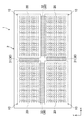
- FIG. 1 is a front view of a solar cell module integrated device according to an embodiment of the present disclosure.
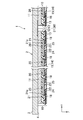
- FIG. 2 is a sectional view taken along line II-II of FIG.
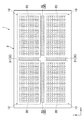
- FIG. 3 is a view corresponding to FIG. 1 and shows a modified example 1 of the embodiment.
- FIG. 4 is a view corresponding to FIG. 1 showing a second modification of the embodiment.
- FIG. 5 is a view corresponding to FIG. 1 showing a third modification of the embodiment.
- FIG. 6 is a view corresponding to FIG. 2 showing a modified example 4 of the embodiment.
- FIG. 7: is sectional drawing which shows the longitudinal cross-section state of the solar cell module integrated device in the modification 5 of embodiment.
- FIG. 1 shows an entire solar cell module integrated device 1 according to an embodiment of the present disclosure.
- This solar cell module integrated device 1 is installed, for example, on the wall surface of a building such as a building.
- the long side direction (direction from the left side to the right side in FIG. 1) of the transparent base material 2 described below is defined as the X-axis direction
- the short side direction of the transparent base material 2 (from the bottom side to the top side in FIG. 1). (Direction toward) is defined as the Y-axis direction
- the thickness direction of the integrated solar cell module device 1 is defined as the Z-axis direction.
- the solar cell module integrated device 1 includes a transparent base material 2.
- the transparent substrate 2 is made of, for example, a glass material having translucency and insulation.
- the transparent substrate 2 is formed in a rectangular plate shape, for example.
- the transparent substrate 2 is formed so that the side along the X direction is longer than the side along the Y direction.
- the material of the transparent base material 2 is not limited to the above glass material, and may be a transparent plastic material such as an acrylic resin material or polyethylene terephthalate (PET).
- the transparent substrate 2 has a first surface 3 and a second surface 4.
- the first surface 3 is a surface for receiving light (for example, sunlight).
- the second surface 4 is located on the opposite side of the first surface 3 in the Z direction.
- the transparent substrate 2 is formed to have a size such that a plurality of solar cell modules 10 described later can be arranged in a state of being spread over the second surface 4.
- the solar cell module integrated device 1 includes a plurality (four in the illustrated example) of solar cell modules 10.
- Each solar cell module 10 is formed in a rectangular shape, for example.
- the plurality of solar cell modules 10 are arranged with a gap therebetween in the surface direction (X direction and Y direction) of the second surface 4 of the transparent substrate 2.
- the plurality of solar cell modules 10 are stacked on the second surface 4 of the transparent substrate 2.
- the solar cell module 10 has a first glass 11.
- the 1st glass 11 is for protecting the cell light-receiving surface 21a of each below-mentioned solar cell 20 sealed in the solar cell module 10.
- the first glass 11 is made of a plate-shaped glass material having translucency and insulation.
- the first glass 11 is formed in a rectangular shape, for example.
- the first glass 11 is laminated on the second surface 4 of the transparent substrate 2.
- the thickness of the first glass 11 is preferably 0.7 mm or more.
- the solar cell module 10 has first and second sealing members 12 and 13.
- the first and second sealing members 12 and 13 are for sealing a plurality of solar battery cells 20 described later in the solar battery module 10.
- Each of the first and second sealing members 12 and 13 is made of a translucent resin material such as ethylene vinyl acetate (EVA).
- the first and second sealing members 12 and 13 are filled so as to fill the space between the first glass 11 and the back side protection member 14 described later in the Z direction.
- the first sealing member 12 is arranged near the first glass 11 in the Z direction.
- the 2nd sealing member 13 is arrange
- a plurality of solar battery cells 20 are mounted on each solar battery module 10.
- the plurality of solar cells 20 are arranged at intervals in the surface direction (X direction and Y direction) of the second surface 4 of the transparent substrate 2.
- the plurality of solar battery cells 20 are sandwiched between the first glass 11 and the back side protection member 14 described later by the first and second sealing members 12 and 13 in the Z direction. It is sealed in the solar cell module 10.
- the solar cell 20 of this embodiment is not particularly limited, but a solar cell of the back electrode type will be described below as an example.
- the solar cell 20 includes a semiconductor substrate 21, an emitter layer 22, a BSF (Back Surface Field) layer 23, a p-type electrode 24, and an n-type electrode 25.
- BSF Back Surface Field
- the semiconductor substrate 21 is a silicon substrate made of, for example, single crystal silicon or polycrystalline silicon.
- the semiconductor substrate 21 has a cell light receiving surface 21a for receiving light (for example, sunlight).
- the surface color of the cell light-receiving surface 21a is, for example, black, blue, brown, gray, purple, or the like.
- the emitter layer 22 is a p-type diffusion layer in which a p-type impurity element is diffused by a thermal diffusion method, for example.
- the BSF layer 23 is an n-type diffusion layer in which an n-type impurity element is diffused by a thermal diffusion method, for example.
- the emitter layer 22 and the BSF layer 23 are formed on the back surface side of the semiconductor substrate 21.
- Each of the p-type electrode 24 and the n-type electrode 25 is a metal electrode layer formed of a metal layer made of aluminum, for example.
- the p-type electrode 24 is formed on the back side of the emitter layer 22.
- the p-type electrode 24 is arranged, for example, near the left end of the semiconductor substrate 21 shown in FIG.
- the n-type electrode 25 is formed on the back side of the BSF layer 23.
- the n-type electrode 25 is disposed, for example, near the right end of the semiconductor substrate 21 shown in FIG.
- the materials for the p-type electrode 24 and the n-type electrode 25 are not limited to the above-mentioned metal layers, and include, for example, a multilayer structure of a transparent conductive oxide layer and a metal layer, a transparent conductive oxide such as indium tin oxide (ITO). May be
- the solar cell module 10 has a back side protection member 14.
- the back side protection member 14 is arranged at a position opposite to the light receiving side of the solar cell module 10.
- the back side protection member 14 of this embodiment is a film 15 made of a resin material.
- the film 15 is colored in a color similar to the color of the cell light-receiving surface 21a of the solar cell 20 (that is, black, blue, brown, gray, purple, etc.).
- the wiring material 16 is attached to each of the p-type electrode 24 and the n-type electrode 25.
- the wiring member 16 is a long conductive wire.
- the wiring member 16 is a ribbon-shaped metal foil or a thin wire metal wire.
- the one end of the wiring member 16 is electrically connected to the p-type electrode 24 of the one solar battery cell 20.
- the other end of the wiring member 16 is electrically connected to the n-type electrode 25 of the other solar battery cell 20 adjacent to the one solar battery cell 20. That is, the plurality of solar battery cells 20 are electrically connected in series via the wiring member 16.
- the electrical connection is not limited to series connection, and one end of the wiring member 16 is electrically connected to the p-type electrode 24 of one solar battery cell 20 and other wiring members 16 are connected.
- the ends may be connected in parallel so as to be electrically connected to the p-type electrode 24 of the other solar battery cell 20 adjacent to the one solar battery cell 20, or an electrical connection in which direct connection and parallel connection are mixed. It may be a connection.
- the transparent substrate 2 is provided with a plurality of colored portions 30.
- the plurality of colored portions 30 are formed on the second surface 4 of the transparent base material 2. 1 and 2, each colored portion 30 is hatched with dots in order to emphasize each colored portion 30.
- Each coloring part 30 is colored in a color similar to the color of the cell light-receiving surface 21a of the solar cell 20.
- each colored portion 30 is one in which a ceramic paint adjusted to any color such as black, blue, brown, gray, and purple is attached to the second surface 4 of the transparent substrate 2.
- the material used for the colored portion 30 is not limited to the ceramic paint, and may be, for example, a dye or a colored film. Further, as the material used for the colored portion 30, a suitable material may be appropriately selected depending on the heat resistant temperature of the member (transparent substrate 2) to be attached.
- the plurality of colored portions 30 are composed of rectangular colored portions 31, 31 and 32, 32.
- Each of the colored portions 31 is arranged at a position including a portion that overlaps the gap between the solar cell modules 10, 10 adjacent to each other in the X direction. Furthermore, each colored part 31 overlaps with the peripheral part of the short side in both of the solar cell modules 10, 10 adjacent to each other.
- Each of the colored portions 32 is arranged at a position including a portion that overlaps the gap between the solar cell modules 10, 10 adjacent to each other in the Y direction. Furthermore, each colored part 32 overlaps with the peripheral part of the long side in both of the solar cell modules 10, 10 adjacent to each other.
- the solar cell modules arranged so as to sandwich the colored portion 30 are designed to emit similar colors as a whole by satisfying the conditions described below.
- a reflection spectrum in the visible light region measured using an analyzer such as a spectrocolorimeter, a spectrocolorimeter, a spectrocolorimeter, or an ultraviolet-visible spectrophotometer is used. ing.
- the measurement value of the color of only diffuse reflection light based on the light incident on the measurement object is defined as the measurement value (L*[x], a*[x], b*[x ]) (Note that, for convenience, identification codes P, Q, and R, which will be described later, are inserted in x).
- the measurement light source used for calculating the reflection color is not particularly limited, and a light source having a known spectral distribution (for example, D50, D55, D65, D75, or C light source) may be used. ..
- the field of view used to calculate the reflection color is not particularly limited, and may be 10 degrees or 2 degrees defined by CIE, for example.
- the numerical value of the color difference between the cell light receiving surface 21a and each colored portion 30 is 30 or less. Also, regarding the color difference between the cell light-receiving surface 21a and the back side protection member 14, and the color difference between each colored portion 30 and the back side protection member 14, it is preferable that each numerical value is 30 or less.
- the measured value of the diffuse reflected light of the light incident on the cell light-receiving surface 21a from the first surface 3 of the transparent substrate 2 is (L * [P], a * [P], b *. [P]).
- the measured values of the diffuse reflection light of the light incident on the respective colored portions 30 from the first surface 3 of the transparent substrate 2 are (L * [Q], a * [Q], b * [Q] ).
- the measured value of the diffuse reflection light of the light D65 which is incident on the back side protection member 14 from the first surface 3 of the transparent substrate 2 is (L * [R], a * [R], b * [R ])
- the colored portion 30 having the same color as the color of each solar cell 20 (cell light-receiving surface 21a) is formed on the second surface 4 of the transparent base material 2, the colored portion 30 having the same color as the color of each solar cell 20 (cell light-receiving surface 21a) is formed. ing. And each coloring part 30 is arrange
- each colored portion 30 is arranged so as to overlap at least a part of the peripheral portion of the solar cell module 10. As a result, the colored portions 30 are brought closer to the solar battery cells 20 arranged in the solar battery module 10, and the gaps between the solar battery cells 20 and the colored portions 30 are narrowed. As a result, the unity of appearance as the solar cell module integrated device 1 is further enhanced.
- Each solar cell 20 also includes an n-type electrode 25 and a p-type electrode 24 formed on the side opposite to the cell light-receiving surface 21a. That is, in each solar cell 20, the n-type electrode 25 and the p-type electrode 24 are not located on the cell light-receiving surface 21a side. As a result, the n-type electrode 25 and the p-type electrode 24 are invisible from the front side of the solar cell module integrated device 1. As a result, the design of the wall surface in the building in which the solar cell module integrated device 1 is installed is further enhanced.
- each colored portion 30 is formed on the second surface 4 of the transparent base material 2. For this reason, the stepped portion between the transparent substrate 2 and each colored portion 30 becomes inconspicuous when the solar cell module integrated device 1 is viewed from the front side. Further, each colored portion 30 is formed on the second surface 4 of the transparent base material 2, so that each solar cell is different from the form in which each colored portion 30 is formed on the first surface 3 of the transparent base material 2. The light receiving area of sunlight with respect to the cell light receiving surface 21a of the cell 20 becomes relatively large. As a result, the photoelectric effect of each solar cell 20 is further enhanced.
- the back side protection member 14 is colored in a color similar to the color of each solar battery cell 20 (cell light receiving surface 21a). That is, each solar cell 20 (cell light-receiving surface 21a), each colored portion 30, and the back side protection member 14 have the same color. As a result, the unity of appearance as the solar cell module integrated device 1 is further improved. As a result, the design of the wall surface in the building in which the solar cell module integrated device 1 is installed is enhanced.
- each solar cell 20 is sealed in the solar cell module 10 in a state of being sandwiched between the first glass 11 and the film 15 (back side protection member 14).
- the weight of each solar cell module 10 is relatively reduced as compared with the case where a glass material is applied as the back side protection member 14 (see Modification 4 described later).
- the options for the thickness of the transparent base material 2 are increased, so that the solar cell module integrated device 1 can be easily customized particularly from the viewpoint of strength.
- the solar battery cell 20 is sealed in the solar battery module 10 while being sandwiched between the first glass 11 and the film 15 (backside protection member 14).
- a difference in thermal expansion between the 1 glass 11 side and the film 15 (back side protection member 14) side is likely to occur. Due to the difference in thermal expansion, the solar cell module 10 is likely to warp.
- the thickness of the first glass 11 is 0.7 mm or more, warpage due to the difference in thermal expansion between the light receiving side and the back side of the solar cell module 10 is prevented in advance.
- the solar cell module integrated device 1 tends to have a uniform appearance. Then, in a building such as a building in which the solar cell module integrated device 1 is installed, the wall surface looks like a single color as a whole. Therefore, the design of the wall surface in the building in which the solar cell module integrated device 1 is installed is improved.
- each of the back side protection members 14 has a similar color to each other. That is, if the respective numerical values of the color difference between the cell light-receiving surface 21a and the back side protection member 14 and the color difference between each colored portion 30 and the back side protection member 14 are 30 or less, the appearance of the solar cell module integrated device 1 will be improved. A sense of unity is more likely to occur. Then, in a building such as a building in which the solar cell module integrated device 1 is installed, the wall surface looks like a single color as a whole. Therefore, the design of the wall surface in the building in which the solar cell module integrated device 1 is installed is improved.
- each colored portion 31 has one of the solar cell modules 10 and 10 adjacent to each other in the X direction (the solar cell module 10 located in the upper left or the lower right in FIG. 3).
- the solar cell module 10 may be overlapped with only the peripheral portion of the short side. That is, in the modification 1, each colored part 31 should just overlap with the peripheral part of at least one short side in the solar cell modules 10 and 10 adjacent to each other.
- each colored portion 32 is overlapped with the peripheral portions of the long sides of both of the solar cell modules 10 adjacent to each other, but the present invention is not limited to this. As shown in FIG. 3, each colored portion 32 may overlap the peripheral portion of the long side of one of the solar cell modules 10 adjacent to each other in the Y direction. That is, in the modification 1, each colored part 32 should just overlap with the peripheral part of at least one long side in the solar cell modules 10 adjacent to each other.
- each colored portion 31 has shown the form overlapping with the peripheral portion of at least one short side in the solar cell modules 10 adjacent to each other, but the present invention is not limited to this form.
- the colored portions 31 may be arranged so as not to overlap the peripheral portions of the short sides of both of the solar cell modules 10 that are adjacent to each other in the X direction.
- each colored portion 32 may be arranged so as not to overlap the peripheral portions of the long sides of both solar cell modules 10, 10 adjacent to each other in the Y direction.
- the colored portions 31, 31 and the colored portions 32, 32 are shown as separated from each other, but the present invention is not limited to this.
- the colored portion 30 may be formed so as to surround the entire periphery of each solar cell module 10.
- the back side protection member 14 is the film 15 made of the resin material, but the back side protection member 14 is not limited to this.
- the backside protection member 14 may include a second glass 17 made of a glass material and a backside colored portion 18. Note that, in FIG. 6, the back side colored portion 18 is hatched with dots as in the case of the colored portion 30.
- the back side coloring part 18 is of the same color as the color of the cell light receiving surface 21a of the solar battery cell 20.
- the back side colored portion 18 shown in FIG. 6 is formed on the front surface side of the second glass 17.
- the back side colored portion 18 may be formed on the back surface of the first glass 11.
- the solar cell 20, the colored portions 30, and the back side protection member 14 have the same color, so that the solar cell module integrated device 1 has an external appearance. Improves the sense of unity. As a result, the design of the wall surface in the building in which the solar cell module integrated device 1 is installed is enhanced.
- the solar battery cell 20 is sealed in the solar battery module 10 while being sandwiched between the first glass 11 and the second glass 17.
- the first glass 11 and the second glass 17 improve the strength of the solar cell module 10 as compared with the above-described embodiment (the form in which the back side protection member 14 is the film 15 made of a resin material).
- the thickness of the second glass 17, like the first glass 11, is preferably 0.7 mm or more.
- the solar battery cells 20 and 20 are arranged at intervals in the X direction, but the present invention is not limited to this.
- a form such as a modified example 5 shown in FIG. 7 may be adopted.
- each solar cell 20 is arranged such that one end of the cell light-receiving surface 21a is inclined with respect to the second surface 4 of the transparent substrate 2 in the Z direction. There is.
- the solar cells 20 and 20 adjacent to each other are arranged such that the end portions of the cell light-receiving surface 21a located in the inclination direction overlap each other. That is, the plurality of solar cells 20 have a so-called single ring type structure.
- n-type electrode 25 is located near the center of the semiconductor substrate 21 shown in FIG. 7 in the X direction.
- the p-type electrode 24 and the n-type electrode 25 are displaced from each other in the X direction.
- one end of the wiring member 16 is electrically connected to the p-type electrode 24 of the one solar battery cell 20.
- the other end of the wiring member 16 is electrically connected to the n-type electrode 25 of the other solar battery cell 20 adjacent to the one solar battery cell 20.
- each colored portion 30 is formed on the second surface 4 of the transparent substrate 2
- the form is not limited to this. That is, the colored portions 30 may be formed on the first surface 3 of the transparent substrate 2.
- the portion where the solar battery cells 20 are not arranged and the portion where the solar battery cells 20 are arranged appear to have the same color.
- the design of the wall surface in the building in which the solar cell module integrated device 1 is installed is enhanced. That is, each colored portion 30 having a color similar to that of the solar cell 20 may be formed on either one of the first surface 3 and the second surface 4 of the transparent substrate 2.
- the solar cell 20 is a back electrode type solar cell in which the n-type electrode 25 and the p-type electrode 24 are arranged on the back surface side of the semiconductor substrate 21.
- a solar battery cell (not shown) in which the n-type electrode 25 is arranged on the cell light-receiving surface 21a side and the p-type electrode 24 is arranged on the back surface side of the semiconductor substrate 21 may be used. Good.
- the solar cell module 10 includes the backside protection member 14, but the present invention is not limited to this. That is, the solar cell module 10 may not include the back side protection member 14.
- Solar cell module integrated device 2 Transparent substrate 3: First surface 4: Second surface 10: Solar cell module 11: First glass 12: First sealing member 13: Second sealing member 14: Backside protection Member 15: Film 16: Wiring material 17: Second glass 18: Back side colored portion 20: Solar cell 21: Semiconductor substrate 21a: Cell light-receiving surface 22: Emitter layer 23: BSF layer 24: P-type electrode 25: N-type electrode 30, 31, 32: Coloring part
Landscapes
- Photovoltaic Devices (AREA)
Abstract
太陽電池モジュール集積デバイス(1)は、第一面および第二面を有する透明基材(2)と、透明基材(2)の第二面に積層配置された複数の太陽電池モジュール(10)と、を含む。各太陽電池モジュール(10)には、セル受光面を有する太陽電池セル(20)が複数実装されている。透明基材(2)の第二面には、各太陽電池セル(20)の色と同系の色となる着色部(30)が形成されている。着色部(30)は、太陽電池モジュール(10),(10)同士の間隙と重なる部分を含む位置に配置されている。
Description
本開示は太陽電池モジュール集積デバイスに関するものである。
従来から、ビルなどの建築物の壁面に設置される太陽電池モジュールとして、例えば特許文献1に示される太陽電池モジュールが知られている。
特許文献1には、透光性パネルと、この透光性パネルと対向する裏面保護材と、透光性パネルと裏面保護材との間に、互いに間隙をおいて配設された複数枚の太陽電池セルと、透光性パネルと裏面保護材との間を充填される充填材と、隣り合う太陽電池セルを電気的に接続する配線部材と、を含む太陽電池モジュールが開示されている。
ところで、特許文献1の太陽電池モジュールを例えばビルの壁面に設置する場合には、複数の太陽電池モジュールを設置する必要がある。しかしながら、隣り合う太陽電池モジュール同士の間隙には太陽電池セルが位置しないため、ビルの壁面において太陽電池セルが位置する部分と太陽電池セルが位置しない部分とでは、外観上の見映えが必然的に異なる。このため、特許文献1の太陽電池モジュールを設置したビルでは、壁面における外観上の統一感が損なわれてしまい、ビル壁面の意匠性が低下してしまうという問題があった。
本開示は斯かる点に鑑みてなされたものであり、その目的は、太陽電池モジュール集積デバイスを設置した建築物における壁面の意匠性を高めることにある。
上記の目的を達成するために、本開示の一実施形態に係る太陽電池モジュール集積デバイスは、光を受光する第一面および第一面の反対側に位置する第二面を有する透明基材と、透明基材の第二面に積層配置されかつ第二面の面方向において互いに間隙をあけて配置された複数の太陽電池モジュールと、を含む。各太陽電池モジュールには、光を受光するためのセル受光面を有する太陽電池セルが複数実装されている。透明基材の第一面および第二面のいずれか一方には、太陽電池セルの色と同系の色となる着色部が形成されている。そして、着色部は、太陽電池モジュール同士の間隙と重なる部分を含む位置に配置されている。
本開示によると、太陽電池モジュール集積デバイスを設置した建築物における壁面の意匠性が高められる。
以下、本開示の実施形態を図面に基づいて詳細に説明する。以下の実施形態の説明は、本質的に例示に過ぎず、本開示、その適用物或いはその用途を制限することを意図するものではない。
図1は、本開示の実施形態に係る太陽電池モジュール集積デバイス1の全体を示している。この太陽電池モジュール集積デバイス1は、例えば、ビルなどの建築物の壁面に設置される。
以下の説明において、後述する透明基材2の長辺方向(図1の左側から右側に向かう方向)をX軸方向とする一方、透明基材2の短辺方向(図1の下側から上側に向かう方向)をY軸方向として定めるものとする。また、図2において、太陽電池モジュール集積デバイス1の厚み方向をZ軸方向として定めるものとする。
(透明基材)
図1に示すように、太陽電池モジュール集積デバイス1は、透明基材2を含む。透明基材2は、例えば、透光性および絶縁性を有するガラス材からなる。透明基材2は、例えば長方形の板状に形成されている。透明基材2は、X方向に沿う辺がY方向に沿う辺よりも長くなるように形成されている。なお、透明基材2の材料としては、上述のガラス材に限られず、例えば、アクリル系樹脂材料やポリエチレンテレフタレート(PET)などの透明性を有するプラスチック材であってもよい。
図1に示すように、太陽電池モジュール集積デバイス1は、透明基材2を含む。透明基材2は、例えば、透光性および絶縁性を有するガラス材からなる。透明基材2は、例えば長方形の板状に形成されている。透明基材2は、X方向に沿う辺がY方向に沿う辺よりも長くなるように形成されている。なお、透明基材2の材料としては、上述のガラス材に限られず、例えば、アクリル系樹脂材料やポリエチレンテレフタレート(PET)などの透明性を有するプラスチック材であってもよい。
図2に示すように、透明基材2は、第一面3および第二面4を有する。第一面3は、光(例えば太陽光)を受光するための面である。第二面4は、Z方向において第一面3の反対側に位置している。透明基材2は、後述する複数の太陽電池モジュール10を第二面4に敷き詰めた状態で配置可能な大きさとなるように形成されている。
(太陽電池モジュール)
図1に示すように、太陽電池モジュール集積デバイス1は、複数(図示例では4つ)の太陽電池モジュール10を含む。各太陽電池モジュール10は、例えば矩形状に形成されている。複数の太陽電池モジュール10は、透明基材2における第二面4の面方向(X方向およびY方向)において互いに間隙をあけて配置されている。図2に示すように、複数の太陽電池モジュール10は、透明基材2の第二面4に積層配置されている。
図1に示すように、太陽電池モジュール集積デバイス1は、複数(図示例では4つ)の太陽電池モジュール10を含む。各太陽電池モジュール10は、例えば矩形状に形成されている。複数の太陽電池モジュール10は、透明基材2における第二面4の面方向(X方向およびY方向)において互いに間隙をあけて配置されている。図2に示すように、複数の太陽電池モジュール10は、透明基材2の第二面4に積層配置されている。
(第1ガラス)
図2に示すように、太陽電池モジュール10は、第1ガラス11を有している。第1ガラス11は、太陽電池モジュール10内に封止された後述する各太陽電池セル20のセル受光面21aを保護するためのものである。
図2に示すように、太陽電池モジュール10は、第1ガラス11を有している。第1ガラス11は、太陽電池モジュール10内に封止された後述する各太陽電池セル20のセル受光面21aを保護するためのものである。
第1ガラス11は、透光性および絶縁性を有する板状のガラス材からなる。第1ガラス11は、例えば矩形状に形成されている。第1ガラス11は、透明基材2の第二面4に積層配置されている。第1ガラス11の厚みは、0.7mm以上であるのが好ましい。
(封止部材)
図2に示すように、太陽電池モジュール10は、第1および第2封止部材12,13を有している。第1および第2封止部材12,13は、後述する複数の太陽電池セル20を太陽電池モジュール10内に封止するためのものである。第1および第2封止部材12,13の各々は、例えばエチレンビニルアセテート(EVA)等の透光性樹脂材料からなる。
図2に示すように、太陽電池モジュール10は、第1および第2封止部材12,13を有している。第1および第2封止部材12,13は、後述する複数の太陽電池セル20を太陽電池モジュール10内に封止するためのものである。第1および第2封止部材12,13の各々は、例えばエチレンビニルアセテート(EVA)等の透光性樹脂材料からなる。
第1および第2封止部材12,13は、Z方向において第1ガラス11と後述する裏側保護部材14との間を埋めるように充填されている。第1封止部材12は、Z方向において第1ガラス11寄りに配置されている。第2封止部材13は、Z方向において後述する裏側保護部材14寄りに配置されている。
(太陽電池セル)
図1に示すように、各太陽電池モジュール10には、太陽電池セル20が複数実装されている。複数の太陽電池セル20は、透明基材2における第二面4の面方向(X方向およびY方向)において互いに間隔をあけて配置されている。
図1に示すように、各太陽電池モジュール10には、太陽電池セル20が複数実装されている。複数の太陽電池セル20は、透明基材2における第二面4の面方向(X方向およびY方向)において互いに間隔をあけて配置されている。
図2に示すように、複数の太陽電池セル20は、Z方向において第1ガラス11と後述する裏側保護部材14との間に挟み込まれた状態で第1および第2封止部材12,13により太陽電池モジュール10内に封止されている。
この実施形態の太陽電池セル20は、特に限定されるものではないが、以下、裏面電極型の太陽電池セルを一例として挙げて説明する。太陽電池セル20は、半導体基板21と、エミッタ層22と、BSF(Back Surface Field)層23と、p型電極24と、n型電極25と、を含む。
半導体基板21は、例えば単結晶シリコンまたは多結晶シリコンからなるシリコン基板である。半導体基板21は、光(例えば太陽光)を受光するためのセル受光面21aを有している。セル受光面21aの表面色は、例えば黒色、青色、茶色、灰色、紫色などである。
エミッタ層22は、例えば熱拡散法によりp型不純物元素を拡散させたp型拡散層である。BSF層23は、例えば熱拡散法によりn型不純物元素を拡散させたn型拡散層である。エミッタ層22およびBSF層23は、半導体基板21の裏面側に形成されている。
p型電極24およびn型電極25の各々は、例えばアルミニウムからなる金属層で形成された金属電極層である。p型電極24は、エミッタ層22の裏側に形成されている。p型電極24は、例えば、図2に示した半導体基板21の左端部寄りに配置されている。n型電極25は、BSF層23の裏側に形成されている。n型電極25は、例えば、図2に示した半導体基板21の右端部寄りに配置されている。
なお、p型電極24およびn型電極25の材料としては、上記金属層に限られず、例えば透明導電性酸化物層と金属層の多層構造、酸化インジウム錫(ITO)などの透明導電性酸化物であってもよい。
(裏側保護部材)
図2に示すように、太陽電池モジュール10は、裏側保護部材14を有している。裏側保護部材14は、太陽電池モジュール10の受光側と反対側の位置に配置されている。この実施形態の裏側保護部材14は、樹脂材料からなるフィルム15である。フィルム15は、太陽電池セル20におけるセル受光面21aの色と同系の色(すなわち、黒色、青色、茶色、灰色、紫色など)に着色されている。
図2に示すように、太陽電池モジュール10は、裏側保護部材14を有している。裏側保護部材14は、太陽電池モジュール10の受光側と反対側の位置に配置されている。この実施形態の裏側保護部材14は、樹脂材料からなるフィルム15である。フィルム15は、太陽電池セル20におけるセル受光面21aの色と同系の色(すなわち、黒色、青色、茶色、灰色、紫色など)に着色されている。
(配線材)
図2に示すように、p型電極24およびn型電極25の各々には、配線材16が取り付けられている。配線材16は、長尺状の導電線である。具体的に、配線材16は、リボン状の金属箔や細線状の金属ワイヤである。
図2に示すように、p型電極24およびn型電極25の各々には、配線材16が取り付けられている。配線材16は、長尺状の導電線である。具体的に、配線材16は、リボン状の金属箔や細線状の金属ワイヤである。
配線材16の一端部は、一方の太陽電池セル20のp型電極24と電気的に接続されている。配線材16の他端部は、一方の太陽電池セル20と隣り合う他方の太陽電池セル20のn型電極25と電気的に接続されている。すなわち、複数の太陽電池セル20は、配線材16を介して直列状に電気的に接続されている。
なお、電気的な接続は、直列接続に限定されるものではなく、配線材16の一端部が、一方の太陽電池セル20のp型電極24と電気的に接続され、その配線材16の他端部が、一方の太陽電池セル20と隣り合う他方の太陽電池セル20のp型電極24と電気的に接続する並列接続されていても構わないし、直接接続および並列接続が混在した電気的な接続であっても構わない。
(着色部)
図1および図2に示すように、透明基材2には、複数の着色部30が設けられている。この実施形態において、複数の着色部30は、透明基材2の第二面4に形成されている。なお、図1および図2では、各着色部30を強調して示すために、各着色部30にドットによるハッチングを付している。
図1および図2に示すように、透明基材2には、複数の着色部30が設けられている。この実施形態において、複数の着色部30は、透明基材2の第二面4に形成されている。なお、図1および図2では、各着色部30を強調して示すために、各着色部30にドットによるハッチングを付している。
各着色部30は、太陽電池セル20におけるセル受光面21aの色と同系の色に着色されている。例えば、各着色部30は、黒色、青色、茶色、灰色、紫色などのいずれかの色に調整されたセラミック塗料が透明基材2の第二面4に付着されたものである。
なお、着色部30に使用される材料は、セラミック塗料に限定されるものではなく、例えば、染料または色付きフィルムであっても構わない。また、着色部30に使用される材料は、付着対象の部材(透明基材2)の耐熱温度等によって、適宜、好適な材料が選択されても構わない。
図1に示すように、この実施形態において、複数の着色部30は、矩形状の着色部31,31および32,32により構成されている。
各着色部31は、X方向において互いに隣り合う太陽電池モジュール10,10同士の間隙と重なる部分を含む位置に配置されている。さらに、各着色部31は、互いに隣り合う太陽電池モジュール10,10の双方における短辺の周縁部と重なっている。
各着色部32は、Y方向において互いに隣り合う太陽電池モジュール10,10同士の間隙と重なる部分を含む位置に配置されている。さらに、各着色部32は、互いに隣り合う太陽電池モジュール10,10の双方における長辺の周縁部と重なっている。
(色差について)
≪CIE1976L*a*b*表色系について≫
着色部30を挟むように配置される太陽電池モジュール同士は、以降に記載の条件を満たすことで、全体的に同系色を発するように設計されている。なお、色を定量的に評価するに際して、分光色彩計、分光色差計、分光測色計、または、紫外可視分光光度計等の分析装置を用いて測定される可視光領域での反射スペクトルを用いている。
≪CIE1976L*a*b*表色系について≫
着色部30を挟むように配置される太陽電池モジュール同士は、以降に記載の条件を満たすことで、全体的に同系色を発するように設計されている。なお、色を定量的に評価するに際して、分光色彩計、分光色差計、分光測色計、または、紫外可視分光光度計等の分析装置を用いて測定される可視光領域での反射スペクトルを用いている。
反射スペクトルに基づく色の数値化については、CIE(国際照明委員会)で規格化されたCIE1976L*a*b*表色系(L*:明[+]~暗[-]、a*:赤味[+]~緑味[-]、b*:黄[+]~青味[-])を用いた。
また、反射色の測定法は、人間の目視の評価と相関性の高い、拡散反射光のみを検出する方法(SCE:Specular Component Exclude)を用いた。そこで、本明細書では、測定対象物に対して入射させた光に基づいた拡散反射光のみの色の測定値を、測定値(L*[x],a*[x],b*[x])とする(なお、xには、便宜上、後述の識別符号P,Q,Rを挿入する)。
また、反射色の算出に使用される測定光源は、特に限定されるものではなく、公知の分光分布を有する光源(例えば、D50、D55、D65、D75、またはC光源)を使用して構わない。また、反射色の算出に使用される視野も、特に限定されるものではなく、例えばCIEによって規定された10度または2度を用いて構わない。
ここで上述した条件について説明する。条件としては、セル受光面21aと各着色部30との色差の数値が30以下であるのが好ましい。また、セル受光面21aと裏側保護部材14との色差、および各着色部30と裏側保護部材14との色差についても、各々の数値が30以下であるのが好ましい。
具体的には、セル受光面21aに対して透明基材2の第一面3から入射させた光の拡散反射光の測定値を、(L*[P]、a*[P]、b*[P])とする。また、各着色部30に対して透明基材2の第一面3から入射させた光の拡散反射光の測定値を、(L*[Q]、a*[Q]、b*[Q])とする。さらに、裏側保護部材14に対して透明基材2の第一面3から入射させた光D65の拡散反射光の測定値を、(L*[R]、a*[R]、b*[R])とする。
そして、セル受光面21aと各着色部30との色差ΔE[PQ]の関係式については、以下の数1により表される。
(数1)
ΔE[PQ]={(L*[P]-L*[Q])2+(a*[P]-a*[Q])2+(b*[P]-b*[Q])2}1/2≦30
ΔE[PQ]={(L*[P]-L*[Q])2+(a*[P]-a*[Q])2+(b*[P]-b*[Q])2}1/2≦30
セル受光面21aと裏側保護部材14との色差ΔE[PR]の関係式については、以下の数2により表される。
(数2)
ΔE[PR]={(L*[P]-L*[R])2+(a*[P]-a*[R])2+(b*[P]-b*[R])2}1/2≦30
ΔE[PR]={(L*[P]-L*[R])2+(a*[P]-a*[R])2+(b*[P]-b*[R])2}1/2≦30
各着色部30と裏側保護部材14との色差ΔE[QR]の関係式については、以下の数3により表される。
(数3)
ΔE[QR]={(L*[Q]-L*[R])2+(a*[Q]-a*[R])2+(b*[Q]-b*[R])2}1/2≦30
ΔE[QR]={(L*[Q]-L*[R])2+(a*[Q]-a*[R])2+(b*[Q]-b*[R])2}1/2≦30
[実施形態の作用効果]
以上のように、太陽電池モジュール集積デバイス1において、透明基材2の第二面4には、各太陽電池セル20(セル受光面21a)の色と同系の色となる着色部30が形成されている。そして、各着色部30は、太陽電池モジュール10,10同士の間隙と重なる部分を含む位置に配置されている。この各着色部30により、太陽電池モジュール集積デバイス1において、太陽電池セル20が位置しない部分の色と、太陽電池セル20が位置する部分の色とが同じ色に見えるようになる。これにより、太陽電池モジュール集積デバイス1としての外観上の統一感が生じる。そして、太陽電池モジュール集積デバイス1を設置したビル等の建築物では、その壁面が全体として単一の色に見えるようになる。したがって、太陽電池モジュール集積デバイス1を設置した建築物における壁面の意匠性が向上する。
以上のように、太陽電池モジュール集積デバイス1において、透明基材2の第二面4には、各太陽電池セル20(セル受光面21a)の色と同系の色となる着色部30が形成されている。そして、各着色部30は、太陽電池モジュール10,10同士の間隙と重なる部分を含む位置に配置されている。この各着色部30により、太陽電池モジュール集積デバイス1において、太陽電池セル20が位置しない部分の色と、太陽電池セル20が位置する部分の色とが同じ色に見えるようになる。これにより、太陽電池モジュール集積デバイス1としての外観上の統一感が生じる。そして、太陽電池モジュール集積デバイス1を設置したビル等の建築物では、その壁面が全体として単一の色に見えるようになる。したがって、太陽電池モジュール集積デバイス1を設置した建築物における壁面の意匠性が向上する。
また、各着色部30は、太陽電池モジュール10における周縁部の少なくとも一部と重なるように配置されている。これにより、各着色部30が太陽電池モジュール10に配置された太陽電池セル20に近づいた状態となり、太陽電池セル20と各着色部30との隙間が狭められる。その結果、太陽電池モジュール集積デバイス1としての外観上の統一感がより一層高められる。
また、各太陽電池セル20は、セル受光面21aの反対側に位置する側に形成されたn型電極25およびp型電極24を含む。すなわち、各太陽電池セル20では、n型電極25およびp型電極24がセル受光面21a側に位置していない。これにより、n型電極25およびp型電極24が、太陽電池モジュール集積デバイス1の正面側から見えなくなる。その結果、太陽電池モジュール集積デバイス1を設置した建築物における壁面の意匠性がより一層高められる。
また、各着色部30は、透明基材2の第二面4に形成されている。このため、透明基材2と各着色部30との段差部分が、太陽電池モジュール集積デバイス1を正面側から見たときに目立ちにくくなる。さらに、各着色部30が透明基材2の第二面4に形成されることにより、各着色部30が透明基材2の第一面3に形成された形態と比較して、各太陽電池セル20のセル受光面21aに対する太陽光の受光領域が相対的に大きくなる。その結果、各太陽電池セル20による光電効果がより一層高められる。
また、裏側保護部材14は、各太陽電池セル20(セル受光面21a)の色と同系の色に着色されている。すなわち、各太陽電池セル20(セル受光面21a)、各着色部30、および裏側保護部材14が同系の色となっている。これにより、太陽電池モジュール集積デバイス1としての外観上の統一感がより一層向上する。その結果、太陽電池モジュール集積デバイス1を設置した建築物における壁面の意匠性が高められる。
また、各太陽電池セル20は、第1ガラス11とフィルム15(裏側保護部材14)との間に挟み込まれた状態で太陽電池モジュール10内に封止されている。かかる構成では、裏側保護部材14としてガラス材を適用した形態(後述の変形例4を参照)と比較して、各太陽電池モジュール10が相対的に軽量化される。その結果、透明基材2における厚みの選択肢が増えることにより、特に強度の観点で太陽電池モジュール集積デバイス1をカスタマイズしやすくなる。
また、この実施形態では、太陽電池セル20が、第1ガラス11とフィルム15(裏側保護部材14)との間に挟み込まれた状態で太陽電池モジュール10内に封止されていることから、第1ガラス11側とフィルム15(裏側保護部材14)側との双方における熱膨張差が生じやすくなる。かかる熱膨張差により、太陽電池モジュール10が反りやすくなってしまう。これに対し、第1ガラス11の厚みが0.7mm以上となっていれば、太陽電池モジュール10の受光側と裏側との熱膨張差による反りが未然に防止される。
また、セル受光面21aと各着色部30との色差の数値が30以下であれば、セル受光面21aと各着色部30とが同系の色であることが客観的に明らかとなる。すなわち、セル受光面21aと各着色部30との色差の数値が30以下であれば、太陽電池モジュール集積デバイス1としての外観上の統一感が生じやすくなる。そして、太陽電池モジュール集積デバイス1を設置したビル等の建築物では、その壁面が全体として単一の色に見えるようになる。したがって、太陽電池モジュール集積デバイス1を設置した建築物における壁面の意匠性が向上する。
さらに、セル受光面21aと裏側保護部材14との色差、および各着色部30と裏側保護部材14との色差の各々の数値が30以下であれば、セル受光面21a、各着色部30、および裏側保護部材14の各々が相互に同系の色であることが客観的に明らかとなる。すなわち、セル受光面21aと裏側保護部材14との色差、および各着色部30と裏側保護部材14との色差の各々の数値が30以下であれば、太陽電池モジュール集積デバイス1としての外観上の統一感がより一層生じやすくなる。そして、太陽電池モジュール集積デバイス1を設置したビル等の建築物では、その壁面が全体として単一の色に見えるようになる。したがって、太陽電池モジュール集積デバイス1を設置した建築物における壁面の意匠性が向上する。
[実施形態の変形例1]
上記実施形態では、各着色部31が、互いに隣り合う太陽電池モジュール10,10の双方における短辺の周縁部と重なる形態を示したが、この形態に限られない。例えば、図3に示す変形例1のように、各着色部31が、X方向において互いに隣り合う太陽電池モジュール10,10の一方(図3の左上に位置する太陽電池モジュール10または右下に位置する太陽電池モジュール10を参照)における短辺の周縁部のみと重なっていてもよい。すなわち、変形例1では、各着色部31が、互いに隣り合う太陽電池モジュール10,10において少なくとも一方の短辺の周縁部と重なっていればよい。
上記実施形態では、各着色部31が、互いに隣り合う太陽電池モジュール10,10の双方における短辺の周縁部と重なる形態を示したが、この形態に限られない。例えば、図3に示す変形例1のように、各着色部31が、X方向において互いに隣り合う太陽電池モジュール10,10の一方(図3の左上に位置する太陽電池モジュール10または右下に位置する太陽電池モジュール10を参照)における短辺の周縁部のみと重なっていてもよい。すなわち、変形例1では、各着色部31が、互いに隣り合う太陽電池モジュール10,10において少なくとも一方の短辺の周縁部と重なっていればよい。
また、上記実施形態では、各着色部32が、互いに隣り合う太陽電池モジュール10,10の双方における長辺の周縁部と重なる形態を示したが、この形態に限られない。図3に示すように、各着色部32が、Y方向において互いに隣り合う太陽電池モジュール10,10の一方における長辺の周縁部と重なっていてもよい。すなわち、変形例1では、各着色部32が、互いに隣り合う太陽電池モジュール10,10において少なくとも一方の長辺の周縁部と重なっていればよい。
[実施形態の変形例2]
上記実施形態および変形例1では、各着色部31が、互いに隣り合う太陽電池モジュール10,10において少なくとも一方の短辺の周縁部と重なる形態を示したが、この形態に限られない。例えば、図4に示す変形例2のように、各着色部31を、X方向において互いに隣り合う太陽電池モジュール10,10の双方における短辺の周縁部と重ならないように配置してもよい。これと同様に、各着色部32を、Y方向において互いに隣り合う太陽電池モジュール10,10の双方における長辺の周縁部と重ならないように配置してもよい。
上記実施形態および変形例1では、各着色部31が、互いに隣り合う太陽電池モジュール10,10において少なくとも一方の短辺の周縁部と重なる形態を示したが、この形態に限られない。例えば、図4に示す変形例2のように、各着色部31を、X方向において互いに隣り合う太陽電池モジュール10,10の双方における短辺の周縁部と重ならないように配置してもよい。これと同様に、各着色部32を、Y方向において互いに隣り合う太陽電池モジュール10,10の双方における長辺の周縁部と重ならないように配置してもよい。
[実施形態の変形例3]
上記実施形態では、着色部31,31および着色部32,32の各々が互いに分離した形態を示したが、この形態に限られない。例えば、図5に示す変形例3のように、着色部30が各太陽電池モジュール10の周縁全体を囲うように形成されていてもよい。
上記実施形態では、着色部31,31および着色部32,32の各々が互いに分離した形態を示したが、この形態に限られない。例えば、図5に示す変形例3のように、着色部30が各太陽電池モジュール10の周縁全体を囲うように形成されていてもよい。
[実施形態の変形例4]
上記実施形態では、裏側保護部材14が樹脂材料からなるフィルム15である形態を示したが、この形態に限られない。例えば、図6に示す変形例4のように、裏側保護部材14は、ガラス材からなる第2ガラス17および裏側着色部18を含んでいてもよい。なお、図6では、着色部30と同様に、裏側着色部18に対してドットによるハッチングを付している。
上記実施形態では、裏側保護部材14が樹脂材料からなるフィルム15である形態を示したが、この形態に限られない。例えば、図6に示す変形例4のように、裏側保護部材14は、ガラス材からなる第2ガラス17および裏側着色部18を含んでいてもよい。なお、図6では、着色部30と同様に、裏側着色部18に対してドットによるハッチングを付している。
裏側着色部18は、太陽電池セル20におけるセル受光面21aの色と同系の色からなる。図6に示した裏側着色部18は、第2ガラス17の表面側に形成されている。なお、裏側着色部18は、第1ガラス11の裏面に形成されていてもよい。
この変形例4であっても、上記実施形態と同様に、太陽電池セル20、各着色部30、および裏側保護部材14が同系の色となることから、太陽電池モジュール集積デバイス1としての外観上の統一感が向上する。その結果、太陽電池モジュール集積デバイス1を設置した建築物における壁面の意匠性が高められる。
そして、太陽電池セル20は、第1ガラス11と第2ガラス17との間に挟み込まれた状態で太陽電池モジュール10内に封止されている。この第1ガラス11および第2ガラス17により、上記実施形態(裏側保護部材14が樹脂材料からなるフィルム15である形態)と比較して、太陽電池モジュール10としての強度が向上する。なお、第2ガラス17の厚みは、第1ガラス11と同様に、0.7mm以上であるのが好ましい。
[実施形態の変形例5]
上記実施形態の太陽電池モジュール10では、太陽電池セル20,20同士をX方向において互いに間隔をあけて配置した形態を示したが、この形態に限られない。例えば、図7に示す変形例5のような形態にしてもよい。
上記実施形態の太陽電池モジュール10では、太陽電池セル20,20同士をX方向において互いに間隔をあけて配置した形態を示したが、この形態に限られない。例えば、図7に示す変形例5のような形態にしてもよい。
具体的に、図7に示すように、各太陽電池セル20は、セル受光面21aの一端部が透明基材2の第二面4に対してZ方向に向かって傾斜するように配置されている。そして、互いに隣り合う太陽電池セル20,20は、セル受光面21aの傾斜方向に位置する端部同士が互いに重なるように配置されている。すなわち、複数の太陽電池セル20は、いわゆるシングリング型の構造となっている。
また、この変形例では、例えばn型電極25のみが、図7に示した半導体基板21におけるX方向の中央寄りに位置している。これにより、太陽電池セル20,20同士がZ方向に重なった状態では、p型電極24およびn型電極25の各々が、X方向において互いにずれるようになる。この状態において、配線材16の一端部は、一方の太陽電池セル20のp型電極24と電気的に接続されている。配線材16の他端部は、一方の太陽電池セル20と隣り合う他方の太陽電池セル20のn型電極25と電気的に接続されている。
このような変形例5では、太陽電池モジュール集積デバイス1の正面側から見たときに、互いに隣り合う太陽電池セル20,20同士の境界位置が識別しにくくなる。これにより、太陽電池モジュール集積デバイス1としての外観上の統一感がより一層向上する。その結果、太陽電池モジュール集積デバイス1を設置した建築物における壁面の意匠性が高められる。
[その他の実施形態]
上記実施形態では、着色部31,31および着色部32,32を設けた形態を示したが、この形態に限られない。例えば、着色部31,31のみを設けた形態としてもよい。あるいは、着色部32,32のみを設けた形態としてもよい。
上記実施形態では、着色部31,31および着色部32,32を設けた形態を示したが、この形態に限られない。例えば、着色部31,31のみを設けた形態としてもよい。あるいは、着色部32,32のみを設けた形態としてもよい。
また、上記実施形態では、各着色部30を透明基材2の第二面4に形成した形態を示したが、この形態に限られない。すなわち、各着色部30を透明基材2の第一面3に形成した形態としてもよい。かかる形態であっても、上記実施形態と同様に、太陽電池セル20が配置されていない部分と太陽電池セル20が配置される部分とが同じ色に見えるようになる。その結果、太陽電池モジュール集積デバイス1を設置した建築物における壁面の意匠性が高められる。すなわち、太陽電池セル20の色と同系の色となる各着色部30が、透明基材2の第一面3および第二面4のいずれか一方に形成されていればよい。
また、上記実施形態では、太陽電池セル20として、n型電極25およびp型電極24を半導体基板21の裏面側に配置した裏面電極型の太陽電池セルを用いた形態を示したが、この形態に限られない。例えば、太陽電池セル20として、n型電極25をセル受光面21a側に配置しかつp型電極24を半導体基板21の裏面側に配置したような太陽電池セル(図示せず)を用いてもよい。
また、上記実施形態では、太陽電池モジュール10が裏側保護部材14を含む形態を示したが、この形態に限られない。すなわち、太陽電池モジュール10が裏側保護部材14を含まない形態としてもよい。
以上、本開示についての実施形態を説明したが、本開示は上述の実施形態のみに限定されず、発明の範囲内で種々の変更が可能である。
1:太陽電池モジュール集積デバイス
2:透明基材
3:第一面
4:第二面
10:太陽電池モジュール
11:第1ガラス
12:第1封止部材
13:第2封止部材
14:裏側保護部材
15:フィルム
16:配線材
17:第2ガラス
18:裏側着色部
20:太陽電池セル
21:半導体基板
21a:セル受光面
22:エミッタ層
23:BSF層
24:p型電極
25:n型電極
30,31,32:着色部
2:透明基材
3:第一面
4:第二面
10:太陽電池モジュール
11:第1ガラス
12:第1封止部材
13:第2封止部材
14:裏側保護部材
15:フィルム
16:配線材
17:第2ガラス
18:裏側着色部
20:太陽電池セル
21:半導体基板
21a:セル受光面
22:エミッタ層
23:BSF層
24:p型電極
25:n型電極
30,31,32:着色部
Claims (11)
- 光を受光する第一面および前記第一面の反対側に位置する第二面を有する透明基材と、
前記透明基材の前記第二面に積層配置されかつ前記第二面の面方向において互いに間隙をあけて配置された複数の太陽電池モジュールと、を含み、
前記各太陽電池モジュールには、光を受光するためのセル受光面を有する太陽電池セルが複数実装されており、
前記第一面および前記第二面のいずれか一方には、前記太陽電池セルの色と同系の色となる着色部が形成されており、
前記着色部は、前記間隙と重なる部分を含む位置に配置されている、太陽電池モジュール集積デバイス。 - 請求項1に記載の太陽電池モジュール集積デバイスにおいて、
前記着色部は、前記太陽電池モジュールにおける周縁部の少なくとも一部と重なるように配置されている、太陽電池モジュール集積デバイス。 - 請求項1または2に記載の太陽電池モジュール集積デバイスにおいて、
前記太陽電池セルは、
前記セル受光面が形成された半導体基板と、
前記セル受光面の反対側に位置する側に形成されたn型電極およびp型電極と、を含む、太陽電池モジュール集積デバイス。 - 請求項3に記載の太陽電池モジュール集積デバイスにおいて、
前記太陽電池セルは、前記セル受光面が前記透明基材の前記第二面に対して傾斜するように配置され、
互いに隣り合う前記太陽電池セルは、前記第二面に対する前記セル受光面の傾斜方向に位置する端部同士が互いに重なるように配置されている、太陽電池モジュール集積デバイス。 - 請求項1~4のいずれか1項に記載の太陽電池モジュール集積デバイスにおいて、
前記着色部は、前記透明基材の前記第二面に形成されている、太陽電池モジュール集積デバイス。 - 請求項1~5のいずれか1項に記載の太陽電池モジュール集積デバイスにおいて、
前記太陽電池モジュールは、前記太陽電池モジュールの受光側と反対側の位置に配置された裏側保護部材を有しており、
前記裏側保護部材は、前記太陽電池セルの色と同系の色に着色されている、太陽電池モジュール集積デバイス。 - 請求項6に記載の太陽電池モジュール集積デバイスにおいて、
前記太陽電池モジュールは、前記透明基材の前記第二面に積層配置されたガラス材からなる第1ガラスを有しており、
前記裏側保護部材は、樹脂材料からなるフィルムであり、
前記太陽電池セルは、前記第1ガラスと前記フィルムとの間に挟み込まれた状態で前記太陽電池モジュール内に封止されている、太陽電池モジュール集積デバイス。 - 請求項6に記載の太陽電池モジュール集積デバイスにおいて、
前記太陽電池モジュールは、前記第二面に積層配置された透明なガラス材からなる第1ガラスを有しており、
前記裏側保護部材は、ガラス材からなる第2ガラスであり、
前記太陽電池セルは、前記第1ガラスと前記第2ガラスとの間に挟み込まれた状態で前記太陽電池モジュール内に封止されている、太陽電池モジュール集積デバイス。 - 請求項7または8に記載の太陽電池モジュール集積デバイスにおいて、
前記第1ガラスの厚みが0.7mm以上である、太陽電池モジュール集積デバイス。 - 請求項1~9のいずれか1項に記載の太陽電池モジュール集積デバイスにおいて、
前記セル受光面と前記着色部との色差の数値が30以下である、太陽電池モジュール集積デバイス。 - 請求項6~9のいずれか1項に記載の太陽電池モジュール集積デバイスにおいて、
前記セル受光面と前記裏側保護部材との色差の数値が30以下であり、かつ前記着色部と前記裏側保護部材との色差の数値が30以下である、太陽電池モジュール集積デバイス。
Priority Applications (1)
| Application Number | Priority Date | Filing Date | Title |
|---|---|---|---|
| JP2020561226A JP7508372B2 (ja) | 2018-12-17 | 2019-11-15 | 太陽電池モジュール集積デバイス |
Applications Claiming Priority (2)
| Application Number | Priority Date | Filing Date | Title |
|---|---|---|---|
| JP2018-235250 | 2018-12-17 | ||
| JP2018235250 | 2018-12-17 |
Publications (1)
| Publication Number | Publication Date |
|---|---|
| WO2020129501A1 true WO2020129501A1 (ja) | 2020-06-25 |
Family
ID=71100456
Family Applications (1)
| Application Number | Title | Priority Date | Filing Date |
|---|---|---|---|
| PCT/JP2019/044929 Ceased WO2020129501A1 (ja) | 2018-12-17 | 2019-11-15 | 太陽電池モジュール集積デバイス |
Country Status (2)
| Country | Link |
|---|---|
| JP (1) | JP7508372B2 (ja) |
| WO (1) | WO2020129501A1 (ja) |
Cited By (3)
| Publication number | Priority date | Publication date | Assignee | Title |
|---|---|---|---|---|
| KR20220145977A (ko) * | 2021-04-22 | 2022-11-01 | 주식회사 에스지에너지 | 은폐성이 우수한 컬러 태양광 모듈, 및 이의 제조방법 |
| WO2023085428A1 (ja) * | 2021-11-15 | 2023-05-19 | 株式会社カネカ | 太陽電池モジュール |
| JP2023072992A (ja) * | 2021-11-15 | 2023-05-25 | 株式会社カネカ | 太陽電池モジュール |
Citations (3)
| Publication number | Priority date | Publication date | Assignee | Title |
|---|---|---|---|---|
| JP2014143384A (ja) * | 2012-12-28 | 2014-08-07 | Dainippon Printing Co Ltd | 太陽電池モジュールおよび太陽電池パネル |
| KR101816164B1 (ko) * | 2016-09-22 | 2018-01-08 | 엘지전자 주식회사 | 태양전지 모듈 |
| US20180151766A1 (en) * | 2016-11-29 | 2018-05-31 | Solarcity Corporation | Anti-corrosion protection in photovoltaic structures |
Family Cites Families (2)
| Publication number | Priority date | Publication date | Assignee | Title |
|---|---|---|---|---|
| JP6484161B2 (ja) | 2015-11-02 | 2019-03-13 | 株式会社豊田自動織機 | 太陽電池モジュール、その実装構造、これを含む車両、および、太陽電池モジュールの製造方法 |
| JP6765077B2 (ja) | 2016-12-22 | 2020-10-07 | パナソニックIpマネジメント株式会社 | 太陽電池モジュール、及び太陽電池モジュールの製造方法 |
-
2019
- 2019-11-15 WO PCT/JP2019/044929 patent/WO2020129501A1/ja not_active Ceased
- 2019-11-15 JP JP2020561226A patent/JP7508372B2/ja active Active
Patent Citations (3)
| Publication number | Priority date | Publication date | Assignee | Title |
|---|---|---|---|---|
| JP2014143384A (ja) * | 2012-12-28 | 2014-08-07 | Dainippon Printing Co Ltd | 太陽電池モジュールおよび太陽電池パネル |
| KR101816164B1 (ko) * | 2016-09-22 | 2018-01-08 | 엘지전자 주식회사 | 태양전지 모듈 |
| US20180151766A1 (en) * | 2016-11-29 | 2018-05-31 | Solarcity Corporation | Anti-corrosion protection in photovoltaic structures |
Cited By (7)
| Publication number | Priority date | Publication date | Assignee | Title |
|---|---|---|---|---|
| KR20220145977A (ko) * | 2021-04-22 | 2022-11-01 | 주식회사 에스지에너지 | 은폐성이 우수한 컬러 태양광 모듈, 및 이의 제조방법 |
| KR102594672B1 (ko) * | 2021-04-22 | 2023-10-27 | 주식회사 에스지에너지 | 은폐성이 우수한 컬러 태양광 모듈, 및 이의 제조방법 |
| WO2023085428A1 (ja) * | 2021-11-15 | 2023-05-19 | 株式会社カネカ | 太陽電池モジュール |
| JPWO2023085428A1 (ja) * | 2021-11-15 | 2023-05-19 | ||
| JP2023072992A (ja) * | 2021-11-15 | 2023-05-25 | 株式会社カネカ | 太陽電池モジュール |
| JP7612047B2 (ja) | 2021-11-15 | 2025-01-10 | 株式会社カネカ | 太陽電池モジュール |
| JP7731767B2 (ja) | 2021-11-15 | 2025-09-01 | 株式会社カネカ | 太陽電池モジュール |
Also Published As
| Publication number | Publication date |
|---|---|
| JP7508372B2 (ja) | 2024-07-01 |
| JPWO2020129501A1 (ja) | 2021-11-04 |
Similar Documents
| Publication | Publication Date | Title |
|---|---|---|
| US11757049B2 (en) | Bifacial solar cell module with backside reflector | |
| US20130206210A1 (en) | Solar battery module, photovoltaic apparatus, and manufacturing method of solar battery module | |
| JP3805996B2 (ja) | 採光型合わせガラス構造太陽電池モジュール及び採光型複層構造太陽電池モジュール | |
| JP7508372B2 (ja) | 太陽電池モジュール集積デバイス | |
| JP2005079170A (ja) | 太陽電池モジュールおよびその製造方法 | |
| CN102800730A (zh) | 光伏装置 | |
| JPWO2014050004A1 (ja) | 太陽電池モジュール | |
| JP7165198B2 (ja) | 均質な色印象を有するソーラーモジュール | |
| WO2018061367A1 (ja) | 太陽電池モジュール | |
| KR101439386B1 (ko) | 채광형 태양전지 모듈 | |
| US11469339B2 (en) | Solar cell module | |
| NL2019628B1 (en) | Photovoltaic module having scattering patterns | |
| JP2005116834A (ja) | 太陽光発電装置 | |
| JP7349979B2 (ja) | 太陽電池モジュール | |
| CN112868106B (zh) | 太阳能电池模块 | |
| JP6661664B2 (ja) | 太陽電池モジュール | |
| KR102953429B1 (ko) | 미디어 펜스형 태양광 모듈 | |
| WO2025243869A1 (ja) | 太陽電池セル及び太陽電池モジュール | |
| ITVI20100048U1 (it) | Pannello fotovoltaico per serre e struttura di copertura fotovoltaica per serra comprendente il pannello |
Legal Events
| Date | Code | Title | Description |
|---|---|---|---|
| 121 | Ep: the epo has been informed by wipo that ep was designated in this application |
Ref document number: 19898898 Country of ref document: EP Kind code of ref document: A1 |
|
| ENP | Entry into the national phase |
Ref document number: 2020561226 Country of ref document: JP Kind code of ref document: A |
|
| NENP | Non-entry into the national phase |
Ref country code: DE |
|
| 122 | Ep: pct application non-entry in european phase |
Ref document number: 19898898 Country of ref document: EP Kind code of ref document: A1 |