WO2020121819A1 - Appareil de traitement de substrats et procédé de traitement de substrats - Google Patents
Appareil de traitement de substrats et procédé de traitement de substrats Download PDFInfo
- Publication number
- WO2020121819A1 WO2020121819A1 PCT/JP2019/046429 JP2019046429W WO2020121819A1 WO 2020121819 A1 WO2020121819 A1 WO 2020121819A1 JP 2019046429 W JP2019046429 W JP 2019046429W WO 2020121819 A1 WO2020121819 A1 WO 2020121819A1
- Authority
- WO
- WIPO (PCT)
- Prior art keywords
- voltage
- power supply
- substrate processing
- supply unit
- processing apparatus
- Prior art date
Links
- 239000000758 substrate Substances 0.000 title claims abstract description 76
- 238000003672 processing method Methods 0.000 title claims description 4
- 238000007493 shaping process Methods 0.000 claims description 16
- 239000003990 capacitor Substances 0.000 claims description 5
- 238000007667 floating Methods 0.000 claims description 3
- 238000010586 diagram Methods 0.000 description 37
- 150000002500 ions Chemical class 0.000 description 26
- 239000004065 semiconductor Substances 0.000 description 11
- 229910052782 aluminium Inorganic materials 0.000 description 5
- 239000004020 conductor Substances 0.000 description 5
- 239000002826 coolant Substances 0.000 description 4
- 230000001133 acceleration Effects 0.000 description 3
- 230000015572 biosynthetic process Effects 0.000 description 3
- 239000000919 ceramic Substances 0.000 description 3
- 238000009792 diffusion process Methods 0.000 description 3
- 238000005516 engineering process Methods 0.000 description 3
- XAGFODPZIPBFFR-UHFFFAOYSA-N aluminium Chemical compound [Al] XAGFODPZIPBFFR-UHFFFAOYSA-N 0.000 description 2
- 238000005530 etching Methods 0.000 description 2
- 239000012212 insulator Substances 0.000 description 2
- 239000000463 material Substances 0.000 description 2
- 238000000034 method Methods 0.000 description 2
- 239000002994 raw material Substances 0.000 description 2
- 239000000498 cooling water Substances 0.000 description 1
- 239000003989 dielectric material Substances 0.000 description 1
- 238000004519 manufacturing process Methods 0.000 description 1
- 229910052751 metal Inorganic materials 0.000 description 1
- 239000002184 metal Substances 0.000 description 1
- 230000000149 penetrating effect Effects 0.000 description 1
- 229910001220 stainless steel Inorganic materials 0.000 description 1
- 239000010935 stainless steel Substances 0.000 description 1
Images


Classifications
-
- C—CHEMISTRY; METALLURGY
- C23—COATING METALLIC MATERIAL; COATING MATERIAL WITH METALLIC MATERIAL; CHEMICAL SURFACE TREATMENT; DIFFUSION TREATMENT OF METALLIC MATERIAL; COATING BY VACUUM EVAPORATION, BY SPUTTERING, BY ION IMPLANTATION OR BY CHEMICAL VAPOUR DEPOSITION, IN GENERAL; INHIBITING CORROSION OF METALLIC MATERIAL OR INCRUSTATION IN GENERAL
- C23C—COATING METALLIC MATERIAL; COATING MATERIAL WITH METALLIC MATERIAL; SURFACE TREATMENT OF METALLIC MATERIAL BY DIFFUSION INTO THE SURFACE, BY CHEMICAL CONVERSION OR SUBSTITUTION; COATING BY VACUUM EVAPORATION, BY SPUTTERING, BY ION IMPLANTATION OR BY CHEMICAL VAPOUR DEPOSITION, IN GENERAL
- C23C16/00—Chemical coating by decomposition of gaseous compounds, without leaving reaction products of surface material in the coating, i.e. chemical vapour deposition [CVD] processes
- C23C16/44—Chemical coating by decomposition of gaseous compounds, without leaving reaction products of surface material in the coating, i.e. chemical vapour deposition [CVD] processes characterised by the method of coating
- C23C16/50—Chemical coating by decomposition of gaseous compounds, without leaving reaction products of surface material in the coating, i.e. chemical vapour deposition [CVD] processes characterised by the method of coating using electric discharges
- C23C16/515—Chemical coating by decomposition of gaseous compounds, without leaving reaction products of surface material in the coating, i.e. chemical vapour deposition [CVD] processes characterised by the method of coating using electric discharges using pulsed discharges
-
- H—ELECTRICITY
- H01—ELECTRIC ELEMENTS
- H01L—SEMICONDUCTOR DEVICES NOT COVERED BY CLASS H10
- H01L21/00—Processes or apparatus adapted for the manufacture or treatment of semiconductor or solid state devices or of parts thereof
- H01L21/02—Manufacture or treatment of semiconductor devices or of parts thereof
- H01L21/04—Manufacture or treatment of semiconductor devices or of parts thereof the devices having potential barriers, e.g. a PN junction, depletion layer or carrier concentration layer
- H01L21/18—Manufacture or treatment of semiconductor devices or of parts thereof the devices having potential barriers, e.g. a PN junction, depletion layer or carrier concentration layer the devices having semiconductor bodies comprising elements of Group IV of the Periodic Table or AIIIBV compounds with or without impurities, e.g. doping materials
- H01L21/30—Treatment of semiconductor bodies using processes or apparatus not provided for in groups H01L21/20 - H01L21/26
- H01L21/302—Treatment of semiconductor bodies using processes or apparatus not provided for in groups H01L21/20 - H01L21/26 to change their surface-physical characteristics or shape, e.g. etching, polishing, cutting
- H01L21/306—Chemical or electrical treatment, e.g. electrolytic etching
- H01L21/3065—Plasma etching; Reactive-ion etching
-
- H—ELECTRICITY
- H05—ELECTRIC TECHNIQUES NOT OTHERWISE PROVIDED FOR
- H05H—PLASMA TECHNIQUE; PRODUCTION OF ACCELERATED ELECTRICALLY-CHARGED PARTICLES OR OF NEUTRONS; PRODUCTION OR ACCELERATION OF NEUTRAL MOLECULAR OR ATOMIC BEAMS
- H05H1/00—Generating plasma; Handling plasma
- H05H1/24—Generating plasma
- H05H1/46—Generating plasma using applied electromagnetic fields, e.g. high frequency or microwave energy
Definitions
- the present disclosure relates to a substrate processing apparatus and a substrate processing method.
- a substrate processing apparatus performs processing on a substrate such as a semiconductor wafer (hereinafter sometimes referred to as “substrate processing”).
- substrate processing for example, the substrate is placed in a chamber (processing container) that is set to a predetermined vacuum degree, and a film-forming source gas is supplied into the chamber to generate plasma. A film is formed on.
- the conventional substrate processing apparatus includes a power supply unit having an AC power supply of a relatively high frequency and a power supply having an AC power supply or a DC power supply of a relatively low frequency in order to control each of the radical density and the ion energy. Two power supply units of the unit are provided. As described above, since the conventional substrate processing apparatus is provided with at least two power supply units, the apparatus scale of the substrate processing apparatus is large.
- the present disclosure provides a technology capable of reducing the scale of a substrate processing apparatus.
- a substrate processing apparatus includes a processing container that can be evacuated, a lower electrode, an upper electrode, and a power supply unit.
- a substrate to be processed can be placed on the lower electrode.
- the upper electrode is arranged to face the lower electrode in the processing container.
- the power supply unit applies a DC pulse voltage to the upper electrode.
- a substrate processing apparatus includes a power supply unit that applies an AC voltage to an upper electrode, a power supply unit that applies an AC voltage to a lower electrode, and a power supply unit that applies a DC voltage to a lower electrode. do not do.
- the apparatus scale of the substrate processing apparatus can be reduced.
- FIG. 1 is a diagram illustrating a configuration example of the substrate processing apparatus according to the first embodiment.
- FIG. 2 is a diagram illustrating a configuration example of the power supply unit according to the first embodiment.
- FIG. 3 is a diagram showing an example of an ideal DC pulse voltage waveform according to the first embodiment.
- FIG. 4 is a diagram showing an example of an actual DC pulse voltage waveform according to the first embodiment.
- FIG. 5 is a diagram illustrating a configuration example of the power supply unit according to the second embodiment.
- FIG. 6 is a diagram showing an example of an ideal DC pulse voltage waveform according to the second embodiment.
- FIG. 7 is a diagram showing an example of an actual DC pulse voltage waveform according to the second embodiment.
- FIG. 8 is a diagram illustrating a configuration example of the substrate processing apparatus according to the third embodiment.
- FIG. 9 is a diagram illustrating an example of voltage limitation according to the third embodiment.
- FIG. 10 is a diagram illustrating an example of voltage limitation according to the third embodiment.
- FIG. 11 is a diagram illustrating a configuration example of the substrate processing apparatus according to the fourth embodiment.
- FIG. 12 is a diagram illustrating a configuration example of the voltage controller according to the fourth embodiment.
- FIG. 13 is a diagram illustrating a configuration example of the voltage controller according to the fourth embodiment.
- FIG. 14 is a diagram illustrating a configuration example of the voltage controller according to the fourth embodiment.
- FIG. 15 is a diagram showing a configuration example of the substrate processing apparatus according to the fifth embodiment.
- FIG. 16 is a diagram illustrating an example of waveform shaping according to the fifth embodiment.
- FIG. 17 is a diagram illustrating an example of waveform shaping according to the fifth embodiment.
- FIG. 18 is a diagram illustrating an example of waveform shaping according to the fifth embodiment.
- FIG. 19 is a diagram illustrating an example of waveform shaping according to the fifth embodiment.
- FIG. 20 is a diagram illustrating an example of waveform shaping according to the fifth embodiment.
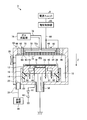
- FIG. 21 is a diagram showing a configuration example of the substrate processing apparatus according to the sixth embodiment.
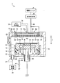
- FIG. 1 is a diagram illustrating a configuration example of the substrate processing apparatus according to the first embodiment.
- the substrate processing apparatus 1 shown in FIG. 1 is configured as a capacitively coupled parallel plate substrate processing apparatus.
- the substrate processing apparatus 1 has a chamber 10 which is a metal processing container made of, for example, aluminum or stainless steel.
- the chamber 10 is grounded for safety.
- a disk-shaped susceptor 12 is horizontally arranged in the chamber 10. On the susceptor 12, a semiconductor wafer W as a substrate to be processed for substrate processing can be placed. The susceptor 12 also functions as a lower electrode. A gate valve 28 that opens and closes a loading/unloading port for the semiconductor wafer W is attached to a sidewall of the chamber 10.
- the susceptor 12 is made of, for example, AlN ceramic or the like, and is supported by an insulating cylindrical support portion 14 extending vertically upward from the bottom of the chamber 10.
- An annular exhaust passage 18 is formed between the side wall of the chamber 10 and a conductive cylindrical support portion (inner wall portion) 16 extending vertically upward from the bottom of the chamber 10 along the outer periphery of the cylindrical support portion 14. There is. An exhaust port 22 is provided at the bottom of the exhaust passage 18.
- An exhaust device 26 is connected to the exhaust port 22 via an exhaust pipe 24.
- the exhaust device 26 has a vacuum pump such as a turbo molecular pump, and reduces the processing space PS in the chamber 10 to a desired vacuum degree.
- the inside of the chamber 10 is preferably maintained at a constant pressure in the range of, for example, 10 mTorr to 3500 mTorr.
- the susceptor 12 used as the lower electrode is grounded via the connecting rod 36.
- a semiconductor wafer W to be processed is placed on the susceptor 12, and an edge ring 38 is provided so as to surround the semiconductor wafer W.
- the edge ring 38 is made of a conductive material (for example, Ni, Al, etc.) and is detachably attached to the upper surface of the susceptor 12.
- An electrostatic chuck 40 for attracting a wafer is provided on the upper surface of the susceptor 12.
- the electrostatic chuck 40 is formed by sandwiching a sheet-shaped or mesh-shaped conductor between film-shaped or plate-shaped dielectrics.
- a DC power source 42 arranged outside the chamber 10 is electrically connected to a conductor inside the electrostatic chuck 40 via an ON/OFF switch 44 and a power supply line 46.
- the semiconductor wafer W is attracted and held on the electrostatic chuck 40 by the Coulomb force generated in the electrostatic chuck 40 by the DC voltage applied from the DC power source 42 to the electrostatic chuck 40.
- an annular coolant chamber 48 extending in the circumferential direction is provided inside the susceptor 12.
- a coolant for example, cooling water
- a chiller unit (not shown)
- the temperature of the semiconductor wafer W on the electrostatic chuck 40 is controlled.
- the heat transfer gas for example, He gas
- the heat transfer gas supply unit is passed through the gas supply pipe 51 and the gas passage 56 in the susceptor 12. And is supplied between the electrostatic chuck 40 and the semiconductor wafer W.
- a disk-shaped inner upper electrode 60 and a ring-shaped outer upper electrode 62 are concentrically provided on the ceiling of the chamber 10 so as to face (that is, face each other) in parallel with the susceptor 12.
- the inner upper electrode 60 has a diameter (diameter) similar to that of the semiconductor wafer W
- the outer upper electrode 62 has a diameter (inner diameter/outer diameter) similar to that of the edge ring 38. ing.
- the inner upper electrode 60 and the outer upper electrode 62 are electrically insulated from each other.
- a ring-shaped insulator 63 made of, for example, ceramic is inserted between the electrodes 60 and 62.
- the inner upper electrode 60 has an electrode plate 64 that faces the susceptor 12 directly in front, and an electrode support 66 that detachably supports the electrode plate 64 from behind (above) it.
- a material for the electrode plate 64 a conductive material such as Ni or Al is preferable.
- the electrode support 66 is made of, for example, alumite-treated aluminum.
- the outer upper electrode 62 also has an electrode plate 68 that faces the susceptor 12, and an electrode support 70 that detachably supports the electrode plate 68 from behind (above) it.
- the electrode plate 68 and the electrode support member 70 are preferably made of the same material as the electrode plate 64 and the electrode support member 66, respectively.
- the inner upper electrode 60 and the outer upper electrode 62 may be collectively referred to as "upper electrodes 60, 62".
- the disk-shaped susceptor 12 that is, the lower electrode
- the disk-shaped upper electrodes 60 and 62 are arranged in parallel to each other and face each other.
- the case where the upper electrodes 60 and 62 are composed of two members, that is, the inner upper electrode 60 and the outer upper electrode 62 has been described as an example.
- the upper electrode may be composed of one member.
- the gas supply unit 76 supplies a film forming raw material gas to the chamber 10 as a processing gas.
- the inner upper electrode 60 is also used as a shower head in order to supply the film forming raw material gas to the processing space PS set between the upper electrodes 60 and 62 and the susceptor 12.
- the gas diffusion chamber 72 is provided inside the electrode support 66, and a large number of gas ejection holes 74 penetrating from the gas diffusion chamber 72 to the susceptor 12 side are formed in the electrode support 66 and the electrode plate 64.
- a gas supply pipe 78 extending from the gas supply unit 76 is connected to the gas introduction port 72 a provided in the upper portion of the gas diffusion chamber 72.
- the shower head may be provided not only on the inner upper electrode 60 but also on the outer upper electrode 62.
- a power supply unit 8 is arranged outside the chamber 10.
- the power supply unit 8 is connected to the upper electrodes 60 and 62 via a power supply line 88 and applies a DC pulse voltage to the upper electrodes 60 and 62.
- a ring-shaped ground part 96 made of a conductive material such as Ni or Al is attached to an appropriate portion of the chamber 10 facing the processing space PS (for example, the outer side of the outer upper electrode 62 in the radial direction). ..
- the ground part 96 is attached to a ring-shaped insulator 98 made of, for example, ceramic, connected to the ceiling wall of the chamber 10, and grounded via the chamber 10.
- control unit The individual operation of each component in the substrate processing apparatus 1 and the overall operation (sequence) of the substrate processing apparatus 1 are controlled by a control unit (not shown).
- control unit the operations of the exhaust device 26, the on/off switch 44, the gas supply unit 76, the chiller unit (not shown), the heat transfer gas supply unit (not shown), etc. are controlled by the control unit (not shown).
- a microcomputer is an example of the control unit.
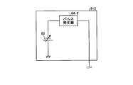
- FIG. 2 is a diagram illustrating a configuration example of the power supply unit according to the first embodiment.
- the power supply unit 8-1 shown in FIG. 2 corresponds to the power supply unit 8 shown in FIG. In FIG. 2, the power supply unit 8-1 has variable DC power supplies 81-1 and 81-2 and a pulse generator 84-1.
- the output terminal of the variable DC power supply 81-1 is connected to the pulse generator 84-1 and the variable DC power supply 81-1 outputs a negative DC voltage (that is, a negative DC voltage) to the pulse generator 84-1.
- the output terminal of the variable DC power supply 81-2 is connected to the pulse generator 84-1, and the variable DC power supply 81-2 outputs a positive DC voltage (that is, a positive DC voltage) to the pulse generator 84-1.
- the pulse generator 84-1 uses a negative DC voltage input from the variable DC power supply 81-1 and a positive DC voltage input from the variable DC power supply 81-2 to generate a DC pulse voltage (that is, a DC pulse voltage).
- the frequency of the DC pulse voltage generated by the pulse generator 84-1 is preferably 10 kHz to 1 MHz, for example.
- the duty ratio of the DC pulse voltage generated by the pulse generator 84-1 is preferably 5% to 95%.
- FIG. 3 is a diagram showing an example of an ideal DC pulse voltage waveform according to the first embodiment.
- V11 negative voltage
- V12 positive voltage
- VC1 positive steady voltage
- WFA1 A DC pulse voltage of a rectangular wave WFA1 having the following is output.
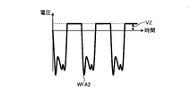
- FIG. 4 is a diagram showing an example of an actual DC pulse voltage waveform according to the first embodiment. That is, the DC pulse voltage having the waveform WFA2 has the overshoot OS11 that exceeds the steady voltage VC1. In particular, when the inductance of the discharge path in the chamber 10 is large, the overshoot OS11 occurs.
- the negative voltage is applied to the upper electrodes 60 and 62 in the periods I11, I13, and I15, and the positive voltage having the overshoot OS11 is generated in the periods I12, I14, and I16. It is applied to the upper electrodes 60 and 62. That is, the pulse generator 84-1 uses the negative DC voltage input from the variable DC power supply 81-1 and the positive DC voltage input from the variable DC power supply 81-2 to generate the DC pulse voltage of the waveform WFA2. By outputting, both positive and negative voltages are applied to the upper electrodes 60 and 62.
- the pulse generator 84-1 outputs the DC pulse voltage of the waveform WFA2, whereby the radical density control and the ion energy control can be alternately performed in time series. That is, it becomes possible to control both the radical density and the ion energy with the single power supply unit 8-1.
- FIG. 5 is a diagram illustrating a configuration example of the power supply unit according to the second embodiment.
- the power supply unit 8-2 shown in FIG. 5 corresponds to the power supply unit 8 shown in FIG.
- the power supply unit 8-2 has a variable DC power supply 80 and a pulse generator 84-2.
- the output terminal of the variable DC power supply 80 is connected to the pulse generator 84-2, and the variable DC power supply 80 outputs a negative DC voltage to the pulse generator 84-2.
- the pulse generator 84-2 uses the negative DC voltage input from the variable DC power supply 80 to generate a DC pulse voltage, and supplies the generated DC pulse voltage to the upper electrodes 60 and 62 via the power supply line 88. To do.
- the frequency of the DC pulse voltage generated by the pulse generator 84-2 is preferably 10 kHz to 1 MHz, for example.
- the duty ratio of the DC pulse voltage generated by the pulse generator 84-2 is preferably 5% to 95%.
- FIG. 6 is a diagram showing an example of an ideal DC pulse voltage waveform according to the second embodiment.
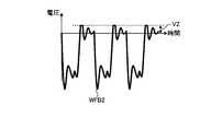
- FIG. 7 is a diagram showing an example of an actual DC pulse voltage waveform according to the second embodiment. That is, the DC pulse voltage having the waveform WFB2 has the overshoot OS21 that exceeds the steady voltage VC2. In particular, when the inductance of the discharge path in the chamber 10 is large, the overshoot OS21 occurs.
- the pulse generator 84-2 outputs the DC pulse voltage of the waveform WFB2 using the negative DC voltage input from the variable DC power supply 80, so that both positive and negative voltages are applied to the upper electrodes 60 and 62. ..
- the pulse generator 84-2 outputs the DC pulse voltage of the waveform WFB2, whereby the radical density control and the ion energy control can be alternately performed in time series. That is, both the radical density and the ion energy can be controlled by the single power supply unit 8-2.
- the substrate processing apparatus 1 includes the chamber 10 that can be evacuated, the susceptor 12 used as the lower electrode, the upper electrodes 60 and 62, and the power supply unit 8.
- a substrate to be processed is placed on the susceptor 12.
- the upper electrodes 60 and 62 are arranged inside the chamber 10 so as to face the susceptor 12.
- the power supply unit 8 applies a DC pulse voltage to the upper electrodes 60 and 62.
- the substrate processing apparatus 1 does not have a power supply unit that applies an AC voltage to the upper electrodes 60 and 62, a power supply unit that applies an AC voltage to the susceptor 12, and a power supply unit that applies a DC voltage to the susceptor 12.
- the power supply unit 8-1 includes a variable DC power supply 81-1 that outputs a negative DC voltage, a variable DC power supply 81-2 that outputs a positive DC voltage, and a pulse generator 84-1.
- the pulse generator 84-1 generates a DC pulse voltage using the negative DC voltage output from the variable DC power supply 81-1 and the positive DC voltage output from the variable DC power supply 81-2.
- the power supply unit 8-2 has the variable DC power supply 80 that outputs a negative DC voltage and the pulse generator 84-2.
- the pulse generator 84-2 uses the negative DC voltage output from the variable DC power supply 80 to generate a DC pulse voltage.
- the substrate processing apparatus 1 does not have a power supply unit other than the power supply unit 8 and can apply both positive and negative voltages to the upper electrodes 60 and 62 with only the single power supply unit 8. Therefore, both the radical density and the ion energy can be controlled without using a power supply unit other than the power supply unit 8. Therefore, the scale of the substrate processing apparatus 1 can be reduced.
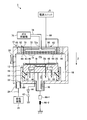
- FIG. 8 is a diagram illustrating a configuration example of the substrate processing apparatus according to the third embodiment.
- the substrate processing apparatus 2 (FIG. 8) according to the third embodiment is different from the substrate processing apparatus 1 (FIG. 1) according to the first embodiment in that it has a voltage limiter 82.
- the voltage limiter 82 limits the maximum value of the positive voltage in the DC pulse voltage output from the power supply unit 8.
- the voltage limiter 82 is realized by using, for example, a Zener diode.
- the voltage limiter 82 sets the maximum value of the positive voltage in the DC pulse voltage having the waveform WFA2 as shown in FIG. Limit to the voltage value VZ.
- the voltage limiter 82 has the maximum value of the positive voltage in the DC pulse voltage having the waveform WFB2 as shown in FIG. Is limited to the voltage value VZ.
- 9 and 10 are diagrams showing an example of voltage limitation according to the third embodiment.
- the potential difference between the upper electrodes 60 and 62 and the susceptor 12 is different from the first and second embodiments. Can be extended for a long period. By making the period during which the potential difference between the upper electrodes 60 and 62 and the susceptor 12 is constant longer than that in the first embodiment, the width of the ion energy distribution can be made narrower than that in the first embodiment.
- FIG. 11 is a diagram illustrating a configuration example of the substrate processing apparatus according to the fourth embodiment.
- the substrate processing apparatus 3 (FIG. 11) according to the fourth embodiment is different from the substrate processing apparatus 1 (FIG. 1) according to the first embodiment in that it has a voltage controller 85.
- the voltage controller 85 controls the magnitude of the positive voltage in the DC pulse voltage output from the power supply unit 8.
- FIG 12, 13, and 14 are diagrams showing a configuration example of the voltage controller according to the fourth embodiment.
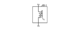
- the voltage controller 85 has the configuration shown in FIG.
- the voltage controller 85-1 shown in FIG. 12 corresponds to the voltage controller 85 shown in FIG.
- the voltage controller 85-1 is formed by the variable coil L connected in series between the power supply unit 8 and the upper electrodes 60 and 62. As the inductance of the variable coil L is increased, the magnitude of the positive voltage in the DC pulse voltage is increased and the ion energy can be increased.
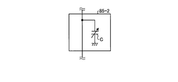
- the voltage controller 85 has the configuration shown in FIG.
- the voltage controller 85-2 shown in FIG. 13 corresponds to the voltage controller 85 shown in FIG.
- the voltage controller 85-2 is formed by the variable capacitor C connected in parallel between the upper electrodes 60 and 62 and the ground. As the capacitance of the variable capacitor C is reduced, the magnitude of the positive voltage in the DC pulse voltage is increased, and the ion energy can be increased.
- the voltage controller 85 has the configuration shown in FIG.
- the voltage controller 85-3 shown in FIG. 14 corresponds to the voltage controller 85 shown in FIG.
- the voltage controller 85-3 is formed by a variable resistor R connected in series between the power supply unit 8 and the upper electrodes 60 and 62. The smaller the resistance value of the variable resistor R, the larger the magnitude of the positive voltage in the DC pulse voltage, and the more the ion energy can be increased.
- the voltage controller 85 is formed by using the variable coil L, the variable capacitor C, or the variable resistor R, but the voltage controller 85 is formed by using a non-variable coil, capacitor, or resistor. 85 may be formed.
- the amount of ion energy can be controlled by controlling the magnitude of the positive voltage in the DC pulse voltage.
- the fourth embodiment has been described above.
- FIG. 15 is a diagram showing a configuration example of the substrate processing apparatus according to the fifth embodiment.
- the substrate processing apparatus 4 (FIG. 15) according to the fifth embodiment is different from the substrate processing apparatus 1 (FIG. 1) according to the first embodiment in that a waveform shaping device 83 is included.
- the waveform shaper 83 shapes the waveform of the DC pulse voltage output from the power supply unit 8.
- 16 to 20 are diagrams showing an example of waveform shaping according to the fifth embodiment.
- the waveform shaper 83 shapes the waveform of the DC pulse voltage output from the power supply unit 8 into a sine wave WF01 as shown in the left diagram of FIG.
- the maximum and minimum values of the DC pulse voltage that is, the maximum and minimum values of the sine wave WF01
- the waveform shaper 83 shapes the waveform of the DC pulse voltage output from the power supply unit 8 into a triangular wave WF02, as shown in FIG.
- the waveform shaper 83 shapes the waveform of the DC pulse voltage output from the power supply unit 8 into a triangular wave WF02, as shown in FIG.
- the waveform shaper 83 shapes the waveform of the DC pulse voltage output from the power supply unit 8 into a rectangular wave WF03, as shown in FIG.
- the waveform shaper 83 shapes the waveform of the DC pulse voltage output from the power supply unit 8 into a rectangular wave WF03, as shown in FIG.
- the substrate processing apparatus 4 since the substrate processing apparatus 4 has the waveform shaping device 83, it is possible to obtain the ion energy distribution according to the waveform after shaping.
- the fifth embodiment has been described above.
- FIG. 21 is a diagram showing a configuration example of the substrate processing apparatus according to the sixth embodiment.
- the substrate processing apparatus 5 (FIG. 21) according to the sixth embodiment is different from the substrate processing apparatus 1 (FIG. 1) according to the first embodiment in that the susceptor 12 is not grounded and is floating.
- the susceptor 12 is grounded by connecting the connector 86-1 and the connector 86-2. On the other hand, by separating the connector 86-1 and the connector 86-2, the susceptor 12 is floated without being grounded.
- the susceptor 12 is floated without being grounded, so that the potential of the susceptor 12 easily follows the potentials of the upper electrodes 60 and 62. Therefore, the potential difference between the upper electrodes 60 and 62 and the susceptor 12 becomes small, so that the acceleration voltage of ions becomes small. Therefore, the ion energy can be reduced by floating the susceptor 12 without being grounded.
- the embodiments of the present disclosure are illustrative in all points and not restrictive. Indeed, the above embodiments may be implemented in various forms. Further, the above-described embodiment may be omitted, replaced, or modified in various forms without departing from the scope and spirit of the claims.
- film formation has been described as an example of substrate processing in the above description, the substrate processing to which the technique of the present disclosure is applicable is not limited to film formation.
- the technique of the present disclosure can be applied to etching, which is one of substrate processing.
Landscapes
- Engineering & Computer Science (AREA)
- Physics & Mathematics (AREA)
- Chemical & Material Sciences (AREA)
- Plasma & Fusion (AREA)
- Power Engineering (AREA)
- Chemical Kinetics & Catalysis (AREA)
- General Physics & Mathematics (AREA)
- Manufacturing & Machinery (AREA)
- Computer Hardware Design (AREA)
- Microelectronics & Electronic Packaging (AREA)
- Spectroscopy & Molecular Physics (AREA)
- Electromagnetism (AREA)
- General Chemical & Material Sciences (AREA)
- Condensed Matter Physics & Semiconductors (AREA)
- Materials Engineering (AREA)
- Mechanical Engineering (AREA)
- Metallurgy (AREA)
- Organic Chemistry (AREA)
- Plasma Technology (AREA)
- Drying Of Semiconductors (AREA)
- Chemical Vapour Deposition (AREA)
Abstract
La présente invention concerne un appareil de traitement de substrats comprenant : un récipient de traitement qui peut être évacué de façon à devenir un dispositif de mise sous vide ; une électrode inférieure ; une électrode supérieure ; et une unité d'alimentation. Un substrat à traiter peut être disposé sur l'électrode inférieure. L'électrode supérieure est disposée de manière à faire face à l'électrode inférieure à l'intérieur du récipient de traitement. L'unité d'alimentation applique une tension continue pulsée à l'électrode supérieure. Par ailleurs, l'appareil de traitement de substrats selon la présente invention ne comprend pas d'unité d'alimentation pour appliquer une tension alternative à l'électrode supérieure, une unité d'alimentation pour appliquer une tension alternative à l'électrode inférieure, ou une unité d'alimentation pour appliquer une tension continue à l'électrode inférieure.
Applications Claiming Priority (2)
| Application Number | Priority Date | Filing Date | Title |
|---|---|---|---|
| JP2018-230882 | 2018-12-10 | ||
| JP2018230882A JP2020095793A (ja) | 2018-12-10 | 2018-12-10 | 基板処理装置及び基板処理方法 |
Publications (1)
| Publication Number | Publication Date |
|---|---|
| WO2020121819A1 true WO2020121819A1 (fr) | 2020-06-18 |
Family
ID=71076375
Family Applications (1)
| Application Number | Title | Priority Date | Filing Date |
|---|---|---|---|
| PCT/JP2019/046429 WO2020121819A1 (fr) | 2018-12-10 | 2019-11-27 | Appareil de traitement de substrats et procédé de traitement de substrats |
Country Status (2)
| Country | Link |
|---|---|
| JP (1) | JP2020095793A (fr) |
| WO (1) | WO2020121819A1 (fr) |
Cited By (18)
| Publication number | Priority date | Publication date | Assignee | Title |
|---|---|---|---|---|
| US11462389B2 (en) | 2020-07-31 | 2022-10-04 | Applied Materials, Inc. | Pulsed-voltage hardware assembly for use in a plasma processing system |
| US11476090B1 (en) | 2021-08-24 | 2022-10-18 | Applied Materials, Inc. | Voltage pulse time-domain multiplexing |
| US11476145B2 (en) | 2018-11-20 | 2022-10-18 | Applied Materials, Inc. | Automatic ESC bias compensation when using pulsed DC bias |
| US11495470B1 (en) | 2021-04-16 | 2022-11-08 | Applied Materials, Inc. | Method of enhancing etching selectivity using a pulsed plasma |
| US11508554B2 (en) | 2019-01-24 | 2022-11-22 | Applied Materials, Inc. | High voltage filter assembly |
| US20230013551A1 (en) * | 2021-07-16 | 2023-01-19 | Tokyo Electron Limited | Plasma processing apparatus and processing method |
| US11569066B2 (en) | 2021-06-23 | 2023-01-31 | Applied Materials, Inc. | Pulsed voltage source for plasma processing applications |
| US11694876B2 (en) | 2021-12-08 | 2023-07-04 | Applied Materials, Inc. | Apparatus and method for delivering a plurality of waveform signals during plasma processing |
| US11699572B2 (en) | 2019-01-22 | 2023-07-11 | Applied Materials, Inc. | Feedback loop for controlling a pulsed voltage waveform |
| US11791138B2 (en) | 2021-05-12 | 2023-10-17 | Applied Materials, Inc. | Automatic electrostatic chuck bias compensation during plasma processing |
| US11798790B2 (en) | 2020-11-16 | 2023-10-24 | Applied Materials, Inc. | Apparatus and methods for controlling ion energy distribution |
| US11810760B2 (en) | 2021-06-16 | 2023-11-07 | Applied Materials, Inc. | Apparatus and method of ion current compensation |
| US11901157B2 (en) | 2020-11-16 | 2024-02-13 | Applied Materials, Inc. | Apparatus and methods for controlling ion energy distribution |
| US11948780B2 (en) | 2021-05-12 | 2024-04-02 | Applied Materials, Inc. | Automatic electrostatic chuck bias compensation during plasma processing |
| US11967483B2 (en) | 2021-06-02 | 2024-04-23 | Applied Materials, Inc. | Plasma excitation with ion energy control |
| US11972924B2 (en) | 2022-06-08 | 2024-04-30 | Applied Materials, Inc. | Pulsed voltage source for plasma processing applications |
| US11984306B2 (en) | 2021-06-09 | 2024-05-14 | Applied Materials, Inc. | Plasma chamber and chamber component cleaning methods |
| US12106938B2 (en) | 2021-09-14 | 2024-10-01 | Applied Materials, Inc. | Distortion current mitigation in a radio frequency plasma processing chamber |
Families Citing this family (1)
| Publication number | Priority date | Publication date | Assignee | Title |
|---|---|---|---|---|
| JP2022057423A (ja) * | 2020-09-30 | 2022-04-11 | 東京エレクトロン株式会社 | プラズマ処理装置 |
Citations (3)
| Publication number | Priority date | Publication date | Assignee | Title |
|---|---|---|---|---|
| JP2000144434A (ja) * | 1998-11-09 | 2000-05-26 | Sekisui Chem Co Ltd | 傾斜機能材料の製造方法 |
| JP2002343768A (ja) * | 2001-05-15 | 2002-11-29 | Tokyo Electron Ltd | プラズマ処理装置 |
| WO2008026712A1 (fr) * | 2006-08-29 | 2008-03-06 | Ngk Insulators, Ltd. | procédé de génération de plasma, procédé de gravure de film en matériau organique, procédé de génération ionique négatif et procédé de traitement par oxydation ou nitruration |
-
2018
- 2018-12-10 JP JP2018230882A patent/JP2020095793A/ja not_active Withdrawn
-
2019
- 2019-11-27 WO PCT/JP2019/046429 patent/WO2020121819A1/fr active Application Filing
Patent Citations (3)
| Publication number | Priority date | Publication date | Assignee | Title |
|---|---|---|---|---|
| JP2000144434A (ja) * | 1998-11-09 | 2000-05-26 | Sekisui Chem Co Ltd | 傾斜機能材料の製造方法 |
| JP2002343768A (ja) * | 2001-05-15 | 2002-11-29 | Tokyo Electron Ltd | プラズマ処理装置 |
| WO2008026712A1 (fr) * | 2006-08-29 | 2008-03-06 | Ngk Insulators, Ltd. | procédé de génération de plasma, procédé de gravure de film en matériau organique, procédé de génération ionique négatif et procédé de traitement par oxydation ou nitruration |
Cited By (23)
| Publication number | Priority date | Publication date | Assignee | Title |
|---|---|---|---|---|
| US11476145B2 (en) | 2018-11-20 | 2022-10-18 | Applied Materials, Inc. | Automatic ESC bias compensation when using pulsed DC bias |
| US12057292B2 (en) | 2019-01-22 | 2024-08-06 | Applied Materials, Inc. | Feedback loop for controlling a pulsed voltage waveform |
| US11699572B2 (en) | 2019-01-22 | 2023-07-11 | Applied Materials, Inc. | Feedback loop for controlling a pulsed voltage waveform |
| US11508554B2 (en) | 2019-01-24 | 2022-11-22 | Applied Materials, Inc. | High voltage filter assembly |
| US11776789B2 (en) | 2020-07-31 | 2023-10-03 | Applied Materials, Inc. | Plasma processing assembly using pulsed-voltage and radio-frequency power |
| US11462388B2 (en) | 2020-07-31 | 2022-10-04 | Applied Materials, Inc. | Plasma processing assembly using pulsed-voltage and radio-frequency power |
| US11462389B2 (en) | 2020-07-31 | 2022-10-04 | Applied Materials, Inc. | Pulsed-voltage hardware assembly for use in a plasma processing system |
| US11848176B2 (en) | 2020-07-31 | 2023-12-19 | Applied Materials, Inc. | Plasma processing using pulsed-voltage and radio-frequency power |
| US11901157B2 (en) | 2020-11-16 | 2024-02-13 | Applied Materials, Inc. | Apparatus and methods for controlling ion energy distribution |
| US11798790B2 (en) | 2020-11-16 | 2023-10-24 | Applied Materials, Inc. | Apparatus and methods for controlling ion energy distribution |
| US11495470B1 (en) | 2021-04-16 | 2022-11-08 | Applied Materials, Inc. | Method of enhancing etching selectivity using a pulsed plasma |
| US11948780B2 (en) | 2021-05-12 | 2024-04-02 | Applied Materials, Inc. | Automatic electrostatic chuck bias compensation during plasma processing |
| US11791138B2 (en) | 2021-05-12 | 2023-10-17 | Applied Materials, Inc. | Automatic electrostatic chuck bias compensation during plasma processing |
| US11967483B2 (en) | 2021-06-02 | 2024-04-23 | Applied Materials, Inc. | Plasma excitation with ion energy control |
| US11984306B2 (en) | 2021-06-09 | 2024-05-14 | Applied Materials, Inc. | Plasma chamber and chamber component cleaning methods |
| US11810760B2 (en) | 2021-06-16 | 2023-11-07 | Applied Materials, Inc. | Apparatus and method of ion current compensation |
| US11887813B2 (en) | 2021-06-23 | 2024-01-30 | Applied Materials, Inc. | Pulsed voltage source for plasma processing |
| US11569066B2 (en) | 2021-06-23 | 2023-01-31 | Applied Materials, Inc. | Pulsed voltage source for plasma processing applications |
| US20230013551A1 (en) * | 2021-07-16 | 2023-01-19 | Tokyo Electron Limited | Plasma processing apparatus and processing method |
| US11476090B1 (en) | 2021-08-24 | 2022-10-18 | Applied Materials, Inc. | Voltage pulse time-domain multiplexing |
| US12106938B2 (en) | 2021-09-14 | 2024-10-01 | Applied Materials, Inc. | Distortion current mitigation in a radio frequency plasma processing chamber |
| US11694876B2 (en) | 2021-12-08 | 2023-07-04 | Applied Materials, Inc. | Apparatus and method for delivering a plurality of waveform signals during plasma processing |
| US11972924B2 (en) | 2022-06-08 | 2024-04-30 | Applied Materials, Inc. | Pulsed voltage source for plasma processing applications |
Also Published As
| Publication number | Publication date |
|---|---|
| JP2020095793A (ja) | 2020-06-18 |
Similar Documents
| Publication | Publication Date | Title |
|---|---|---|
| WO2020121819A1 (fr) | Appareil de traitement de substrats et procédé de traitement de substrats | |
| CN109411322B (zh) | 等离子体处理方法和等离子体处理装置 | |
| KR102539151B1 (ko) | 기판 처리 방법 | |
| US20220084787A1 (en) | Plasma processing apparatus and plasma processing method | |
| US12112925B2 (en) | Plasma processing apparatus | |
| WO2019239872A1 (fr) | Appareil de formation de film et procédé de nettoyage d'appareil de formation de film | |
| US12033832B2 (en) | Plasma processing method and plasma processing apparatus | |
| US11430636B2 (en) | Plasma processing apparatus and cleaning method | |
| US20190122863A1 (en) | Plasma processing apparatus | |
| US20240006154A1 (en) | Plasma processing method and plasma processing apparatus | |
| US8366833B2 (en) | Plasma processing apparatus and plasma processing method | |
| TW201533837A (zh) | 於載置台吸附被吸附物之方法及處理裝置 | |
| US11923171B2 (en) | Plasma processing apparatus and plasma processing method | |
| US20220108878A1 (en) | Plasma processing apparatus and plasma processing method | |
| US20220139672A1 (en) | Plasma processing apparatus and plasma processing method | |
| US11887817B2 (en) | Plasma processing apparatus and plasma processing method | |
| US12020899B2 (en) | Plasma processing apparatus and plasma processing method | |
| US11417502B2 (en) | Plasma processing system and substrate processing method | |
| KR20220162086A (ko) | 플라스마 처리 장치 | |
| US20210296093A1 (en) | Plasma processing apparatus | |
| US20210296091A1 (en) | Inspection method, inspection apparatus, and plasma processing apparatus | |
| JP2022075506A (ja) | プラズマ処理装置及びプラズマ処理方法 | |
| US20230377844A1 (en) | Plasma processing apparatus and plasma processing method | |
| WO2019230526A1 (fr) | Dispositif et procédé de formation de film | |
| US20240145218A1 (en) | Plasma processing apparatus and plasma processing method |
Legal Events
| Date | Code | Title | Description |
|---|---|---|---|
| 121 | Ep: the epo has been informed by wipo that ep was designated in this application |
Ref document number: 19894677 Country of ref document: EP Kind code of ref document: A1 |
|
| NENP | Non-entry into the national phase |
Ref country code: DE |
|
| 122 | Ep: pct application non-entry in european phase |
Ref document number: 19894677 Country of ref document: EP Kind code of ref document: A1 |