WO2020121663A1 - Elastic wave device - Google Patents
Elastic wave device Download PDFInfo
- Publication number
- WO2020121663A1 WO2020121663A1 PCT/JP2019/042190 JP2019042190W WO2020121663A1 WO 2020121663 A1 WO2020121663 A1 WO 2020121663A1 JP 2019042190 W JP2019042190 W JP 2019042190W WO 2020121663 A1 WO2020121663 A1 WO 2020121663A1
- Authority
- WO
- WIPO (PCT)
- Prior art keywords
- electrode
- facing
- comb
- electrode fingers
- fingers
- Prior art date
- Legal status (The legal status is an assumption and is not a legal conclusion. Google has not performed a legal analysis and makes no representation as to the accuracy of the status listed.)
- Ceased
Links
Images

Classifications
-
- H—ELECTRICITY
- H03—ELECTRONIC CIRCUITRY
- H03H—IMPEDANCE NETWORKS, e.g. RESONANT CIRCUITS; RESONATORS
- H03H9/00—Networks comprising electromechanical or electro-acoustic elements; Electromechanical resonators
- H03H9/02—Details
- H03H9/125—Driving means, e.g. electrodes, coils
- H03H9/145—Driving means, e.g. electrodes, coils for networks using surface acoustic waves
- H03H9/14538—Formation
-
- H—ELECTRICITY
- H03—ELECTRONIC CIRCUITRY
- H03H—IMPEDANCE NETWORKS, e.g. RESONANT CIRCUITS; RESONATORS
- H03H9/00—Networks comprising electromechanical or electro-acoustic elements; Electromechanical resonators
- H03H9/02—Details
- H03H9/02535—Details of surface acoustic wave devices
- H03H9/02818—Means for compensation or elimination of undesirable effects
-
- H—ELECTRICITY
- H03—ELECTRONIC CIRCUITRY
- H03H—IMPEDANCE NETWORKS, e.g. RESONANT CIRCUITS; RESONATORS
- H03H9/00—Networks comprising electromechanical or electro-acoustic elements; Electromechanical resonators
- H03H9/02—Details
- H03H9/02535—Details of surface acoustic wave devices
- H03H9/02992—Details of bus bars, contact pads or other electrical connections for finger electrodes
-
- H—ELECTRICITY
- H03—ELECTRONIC CIRCUITRY
- H03H—IMPEDANCE NETWORKS, e.g. RESONANT CIRCUITS; RESONATORS
- H03H9/00—Networks comprising electromechanical or electro-acoustic elements; Electromechanical resonators
- H03H9/02—Details
- H03H9/125—Driving means, e.g. electrodes, coils
- H03H9/145—Driving means, e.g. electrodes, coils for networks using surface acoustic waves
- H03H9/14538—Formation
- H03H9/14541—Multilayer finger or busbar electrode
-
- H—ELECTRICITY
- H03—ELECTRONIC CIRCUITRY
- H03H—IMPEDANCE NETWORKS, e.g. RESONANT CIRCUITS; RESONATORS
- H03H9/00—Networks comprising electromechanical or electro-acoustic elements; Electromechanical resonators
- H03H9/02—Details
- H03H9/125—Driving means, e.g. electrodes, coils
- H03H9/145—Driving means, e.g. electrodes, coils for networks using surface acoustic waves
- H03H9/14544—Transducers of particular shape or position
- H03H9/14552—Transducers of particular shape or position comprising split fingers
-
- H—ELECTRICITY
- H03—ELECTRONIC CIRCUITRY
- H03H—IMPEDANCE NETWORKS, e.g. RESONANT CIRCUITS; RESONATORS
- H03H9/00—Networks comprising electromechanical or electro-acoustic elements; Electromechanical resonators
- H03H9/46—Filters
- H03H9/54—Filters comprising resonators of piezoelectric or electrostrictive material
-
- H—ELECTRICITY
- H03—ELECTRONIC CIRCUITRY
- H03H—IMPEDANCE NETWORKS, e.g. RESONANT CIRCUITS; RESONATORS
- H03H9/00—Networks comprising electromechanical or electro-acoustic elements; Electromechanical resonators
- H03H9/46—Filters
- H03H9/64—Filters using surface acoustic waves
Definitions
- the present invention relates to an acoustic wave device.
- Patent Document 1 discloses an example of an acoustic wave device.
- an IDT electrode Interdigital Transducer
- the IDT electrode is made of Al-Cu alloy. In this way, the electrode fingers of the IDT electrodes are uniformly formed of the same material.
- An object of the present invention is to provide an elastic wave device capable of effectively suppressing IMD.
- a first comb tooth that includes a piezoelectric substrate and an IDT electrode provided on the piezoelectric substrate, each of the IDT electrodes including a main electrode layer is provided.
- a comb-shaped electrode and a second comb-shaped electrode wherein the first comb-shaped electrode includes a first bus bar and a plurality of first electrode fingers whose one end is connected to the first bus bar.
- the second comb-teeth-shaped electrode has a second busbar and a plurality of first electrodes connected at one end to the second busbar and interposing with the plurality of first electrode fingers.
- a second portion in which the IDT electrode has a first portion in which the main electrode layer is made of a first metal and a second electrode in which the main electrode layer is made of a second metal.
- the first electrode fingers and the second comb-teeth-shaped electrodes each have a first facing portion that is a portion facing each other across a gap
- the second electrode fingers and the first comb-teeth-shaped electrodes each have a second facing portion that is a portion facing each other with a gap, and the first facing portions of the plurality of first electrode fingers.
- the first facing portion of the second comb-shaped electrode the second facing portion of the plurality of second electrode fingers, and the second facing portion of the first comb-shaped electrode.
- At least one of the facing portions is the second portion, the portion of the IDT electrode other than the second portion is the first portion, and the density of the second metal is the first metal. Higher than the density of.
- a first comb including a piezoelectric substrate and an IDT electrode provided on the piezoelectric substrate, each of the IDT electrodes including a main electrode layer is provided.
- a tooth-shaped electrode and a second comb-shaped electrode wherein the first comb-shaped electrode includes a first bus bar and a plurality of first electrode fingers whose one end is connected to the first bus bar.
- a second portion having a second electrode finger wherein the IDT electrode has a first portion in which the main electrode layer is made of a first metal and a second portion in which the main electrode layer is made of a second metal.
- Two portions, and the plurality of first electrode fingers and the second comb tooth-shaped electrodes each have a first facing portion that is a portion facing each other with a gap
- the second electrode finger and the first comb-tooth-shaped electrode each have a second facing portion that is a portion facing each other with a gap, and the first facing of the plurality of first electrode fingers is performed.
- At least one of the facing portions is the second portion, a portion of the IDT electrode other than the second portion is the first portion, and the Young's modulus of the second metal is the first portion. Higher than Young's modulus of metal.
- an elastic wave device capable of effectively suppressing IMD.
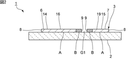
- FIG. 1 is a plan view of an elastic wave device according to a first embodiment of the present invention.
- FIG. 2 is a sectional view taken along the line II in FIG.
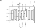
- FIG. 3 is a plan view of an elastic wave device according to a first modification of the first embodiment of the present invention.
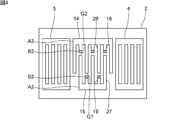
- FIG. 4 is a plan view of an elastic wave device according to a second modification of the first embodiment of the present invention.
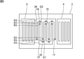
- FIG. 5 is a plan view of an elastic wave device according to a third modification of the first embodiment of the present invention.
- FIG. 6 is a plan view of an elastic wave device according to a fourth modification of the first embodiment of the present invention.
- FIG. 7 is a plan view of an elastic wave device according to a fifth modification of the first embodiment of the present invention.
- FIG. 1 is a plan view of an elastic wave device according to a first embodiment of the present invention.
- FIG. 2 is a sectional view taken along the line II in FIG.
- FIG. 3 is a plan view of an elastic wave device according
- FIG. 8 is a cross-sectional view corresponding to the portion shown in FIG. 2 of an elastic wave device according to a sixth modification of the first embodiment of the present invention.
- FIG. 9 is a sectional view of an elastic wave device according to a seventh modification of the first embodiment of the present invention, which corresponds to the portion shown in FIG.
- FIG. 10 is a cross-sectional view corresponding to the portion shown in FIG. 2 of the elastic wave device according to the eighth modification of the first embodiment of the present invention.
- FIG. 1 is a plan view of an elastic wave device according to a first embodiment of the present invention.
- FIG. 2 is a sectional view taken along the line II in FIG. In FIG. 1, a second portion described later is shown by hatching. The same applies to each plan view other than FIG.
- the acoustic wave device 1 has a piezoelectric substrate 2.
- the piezoelectric substrate 2 is a piezoelectric substrate composed of only a piezoelectric layer.
- an appropriate piezoelectric single crystal or piezoelectric ceramic can be used. More specifically, as the material of the piezoelectric substrate 2, for example, lithium niobate, lithium tantalate, zinc oxide, aluminum nitride, quartz (SiO 2 ), sapphire, or the like can be used.
- the piezoelectric substrate 2 may be a laminated body including a piezoelectric layer.
- the elastic wave device 1 of the present embodiment is an elastic wave resonator.
- the elastic wave device 1 according to the present invention may be a filter device including an elastic wave resonator.
- the IDT electrode 3 has a first comb-teeth electrode 6 and a second comb-teeth electrode 7.
- the first comb-teeth-shaped electrode 6 has a first bus bar 14 and a plurality of first electrode fingers 16 each having one end connected to the first bus bar 14.
- the second comb-tooth-shaped electrode 7 has a second bus bar 15 and a plurality of second electrode fingers 17 each having one end connected to the second bus bar 15.
- the plurality of first electrode fingers 16 and the plurality of second electrode fingers 17 are interleaved with each other.
- the plurality of first electrode fingers 16 are opposed to the second comb tooth-shaped electrode 7 with a first gap G1 therebetween.
- the plurality of second electrode fingers 17 face the first comb tooth-shaped electrode 6 with a second gap G2 therebetween.
- each of the first comb-teeth-shaped electrodes 6 is connected to the first bus bar 14, and the plurality of first electrode fingers 17 are opposed to the plurality of second electrode fingers 17 with a second gap G2 therebetween. It has dummy electrode fingers 18.
- One end of each of the second comb-teeth-shaped electrodes 7 is connected to the second bus bar 15, and the plurality of second comb-shaped electrodes 7 are opposed to the plurality of first electrode fingers 16 with the first gap G1 therebetween. It has dummy electrode fingers 19.
- the plurality of first electrode fingers 16 and the second comb-teeth-shaped electrodes 7 each have a first facing portion that is a portion facing each other across the first gap G1.
- the first facing portions of the plurality of first electrode fingers 16 are tip portions of the plurality of first electrode fingers 16.
- the first facing portion of the second comb tooth-shaped electrode 7 is the tip portion of the plurality of second dummy electrode fingers 19 in the present embodiment.
- the plurality of second electrode fingers 17 and the first comb tooth-shaped electrode 6 each have a second facing portion that is a portion facing each other across the second gap G2.
- the second facing portions of the plurality of second electrode fingers 17 are tip portions of the plurality of second electrode fingers 17.
- the second facing portion of the first comb tooth-shaped electrode 6 is the tip portion of the plurality of first dummy electrode fingers 18 in the present embodiment.
- the IDT electrode 3 does not necessarily have to have the first dummy electrode finger 18 and the second dummy electrode finger 19.
- the first comb-teeth electrode 6 and the second comb-teeth electrode 7 each have a main electrode layer.
- the main electrode layer means an electrode layer which accounts for 50% by weight or more.
- the IDT electrode 3 includes a first portion A having a main electrode layer 8 made of a first metal and a second portion A having a main electrode layer 9 made of a second metal. And part B. More specifically, as shown in FIG. 1, the second portion B of the IDT electrode 3 includes a plurality of first electrode fingers 16, a plurality of second electrode fingers 17, and a plurality of first dummy electrode fingers. 18 and the tips of the plurality of second dummy electrode fingers 19, respectively.
- both of the first facing portions of the plurality of first electrode fingers 16 and the first facing portions of the second comb tooth-shaped electrodes 7 and the plurality of second electrode fingers are provided.
- Both the second facing portion 17 and the second facing portion of the first comb tooth-shaped electrode 6 are the second portion B.
- At least one of the first facing portions of the plurality of first electrode fingers 16 and the first facing portion of the second comb-tooth-shaped electrode 7 and the second facing portions of the plurality of second electrode fingers 17 are arranged. It is sufficient that at least one of the second portion and the second facing portion of the first comb-teeth electrode 6 is the second portion B.
- At least one of the second facing portions of the comb-shaped electrode 6 may be the second portion B.
- the portion other than the second portion B of the IDT electrode 3 is the first portion A. More specifically, in the present embodiment, each of the plurality of first electrode fingers 16, the plurality of second electrode fingers 17, the plurality of first dummy electrode fingers 18, and the plurality of second dummy electrode fingers 19 is provided.
- the first bus bar 14 and the second bus bar 15 are parts other than the tip end of the first part A.
- an electrode layer of a wiring electrode connected to other elements or the like may be provided on the first bus bar 14 and the second bus bar 15 of the IDT electrode 3. It should be pointed out that the electrode layer of this wiring electrode and the first bus bar 14 and the second bus bar 15 of the IDT electrode 3 in the present invention are separate.
- the density of the second metal is higher than the density of the first metal, and the Young's modulus of the second metal is higher than the Young's modulus of the first metal.
- the relationship between the first metal and the second metal is that the density of the second metal is higher than the density of the first metal, and the Young's modulus of the second metal is higher than the Young's modulus of the first metal. It suffices if at least one of the high relationships. More specifically, for example, when the first metal is Al, the second metal may be Ti, Cu, Mo, Cr, Ru, W, Pt, Ta, Co, Ni, Au or Mn. You can select any of these. However, the first metal and the second metal may be alloys.
- the IDT electrode 3 can be formed by, for example, a sputtering method or a vacuum evaporation method.
- the second portion B may be formed after forming the first portion A, and the first portion A may be formed after forming the second portion B.
- the first portion A and the second portion B of the IDT electrode 3 are each made of a single metal layer.
- the reflector 4 and the reflector 5 are also made of a single metal layer.
- the first portion A and the second portion B of the IDT electrode 3, the reflector 4 and the reflector 5 may be formed of a laminated metal film in which a plurality of metal layers are laminated.
- the feature of this embodiment is that it has the following configuration.
- the IDT electrode 3 has a first portion A in which a main electrode layer is made of a first metal and a second portion B in which a main electrode layer is made of a second metal.
- at least one of the second facing portions of the first comb-teeth electrode 6 is the second portion B.
- the portion of the IDT electrode 3 other than the second portion B is the first portion A.
- the relationship between the first metal and the second metal is such that the density of the second metal is higher than the density of the first metal, and the Young's modulus of the second metal is higher than the Young's modulus of the first metal. At least one of the high relationships. Thereby, IMD can be suppressed effectively. This will be explained below.
- the second-order nonlinear signal of the IMD signals mainly occurs in the first gap G1 and the second gap G2 in the IDT electrode 3.
- the IDT electrode 3 itself has a first portion A and a second portion B made of different metals.
- the first portion A and the second portion B are continuously formed and electrically connected.
- the first facing portion and the second facing portion of the IDT electrode 3, which face each other across the gaps, are mainly made of the second metal which is heavier or has a higher Young's modulus than the first metal and the second metal. It is a second portion B on which the electrode layer 9 is formed. That is, the heavy or high Young's modulus second metal is directly arranged on the piezoelectric substrate 2 in the region of the IDT electrode 3 in contact with each of the gaps.
- the second metal which is heavy or has a high Young's modulus
- both of the first facing portions of the plurality of first electrode fingers 16 and the first facing portions of the second comb-teeth-shaped electrode 7 and the plurality of second electrode fingers 17 are provided. It is preferable that both the second facing portion and the second facing portion of the first comb-shaped electrode 6 are the second portion B. Thereby, the strain in the first gap G1 and the second gap G2 can be further suppressed, and the IMD can be further suppressed.
- first modification example and a second modification example of the first embodiment in which the arrangement of the second portion is different, are shown. More specifically, in the first modified example and the second modified example, one of the first facing portions of the plurality of first electrode fingers and the first facing portion of the second comb-teeth-shaped electrode is provided. , One of the second facing portions of the plurality of second electrode fingers and the second facing portion of the first comb-shaped electrode is a second portion. Also in the first modified example and the second modified example, distortion in the first gap and the second gap can be effectively suppressed, and IMD can be effectively suppressed.
- FIG. 3 is a plan view of an elastic wave device according to a first modified example of the first embodiment.
- FIG. 4 is a plan view of an elastic wave device according to a second modification of the first embodiment.
- the second portion B1 is the tip portions of the plurality of first electrode fingers 16 and the tip portions of the plurality of second electrode fingers 17.
- the first portion A1 is a portion other than the tip of each of the plurality of first electrode fingers 16 and the plurality of second electrode fingers 17, the plurality of first dummy electrode fingers 28, and the plurality of second dummy electrodes.
- at least one of the tip portions of the plurality of first electrode fingers 16 and the tip portions of the plurality of second electrode fingers 17 may be the second portion B1.
- the second portions B2 are the tip portions of the plurality of first dummy electrode fingers 18 and the tip portions of the plurality of second dummy electrode fingers 19.
- the first portion A2 is a portion other than the tip of each of the plurality of first dummy electrode fingers 18 and the plurality of second dummy electrode fingers 19, the plurality of first electrode fingers 26, and the plurality of second electrodes.
- the IDT electrode does not have to have the first dummy electrode finger and the second dummy electrode finger.
- third to fifth modified examples of the first embodiment which do not have the first dummy electrode finger and the second dummy electrode finger, will be shown. Also in the third to fifth modified examples, distortion in the first gap and the second gap can be effectively suppressed, and IMD can be effectively suppressed.
- the plurality of first electrode fingers 16 and the second bus bar 35 are opposed to each other with the first gap G1 therebetween.
- the first facing portion of the second comb-shaped electrode 37 is a portion facing the respective first electrode fingers 16 of the second bus bar 35.
- the first facing portions of the plurality of first electrode fingers 16 are tip portions of the plurality of first electrode fingers 16.
- the plurality of second electrode fingers 17 and the first bus bar 34 face each other with the second gap G2 therebetween.
- the second facing portion of the first comb tooth-shaped electrode 36 is a portion facing the respective second electrode fingers 17 of the first bus bar 34.
- the second facing portions of the plurality of second electrode fingers 17 are tip portions of the plurality of second electrode fingers 17.
- each first facing portion and each second facing portion is the same as this modified example.
- both of the first facing portions of the plurality of first electrode fingers 16 and the first facing portions of the second comb tooth-shaped electrodes 37 and the first facing portions of the plurality of second electrode fingers 17 are provided. Both of the two facing portions and the second facing portion of the first comb-shaped electrode 36 are the second portion B3. On the other hand, the portions other than the respective tip portions of the plurality of first electrode fingers 16 and the plurality of second electrode fingers 17 are the first portion A3. Furthermore, the portion of the first bus bar 34 other than the portion facing the second electrode fingers 17 and the portion of the second bus bar 35 other than the portion facing the first electrode fingers 16 are also the first portions. Is part A3.
- the second portion B4 is the tip portions of the plurality of first electrode fingers 16 and the tip portions of the plurality of second electrode fingers 17.
- the first portion A4 is a portion other than the tip portion of each of the plurality of first electrode fingers 16 and the plurality of second electrode fingers 17, the first bus bar 14, and the second bus bar 15.
- a portion of the first bus bar 34 facing each second electrode finger 27 and each first electrode finger 26 of the second bus bar 35 are provided.
- the facing portion is the second portion B5.
- the plurality of first electrode fingers 26 and the plurality of second electrode fingers 27 are the first portion A5.
- the portion of the first bus bar 34 other than the portion facing the second electrode fingers 27 and the portion of the second bus bar 35 other than the portion facing the first electrode fingers 26 are also the first portions. Is part A5.
- the IDT electrode 3 is composed of a single metal layer.
- the IDT electrode 3 may have a layer other than the main electrode layer.
- the IDT electrode 43 includes the main electrode layer 8 of the first portion A6, the main electrode layer 9 of the second portion B6, and the piezoelectric substrate 2. It has an adhesion layer 44 provided between and. Thereby, the adhesiveness between the IDT electrode 43 and the piezoelectric substrate 2 can be enhanced more reliably.
- the second metal having a high weight or a high Young's modulus is arranged at a position close to the piezoelectric substrate 2 in a region in contact with each gap in the IDT electrode 3, the second embodiment is different from the first embodiment. Similarly, distortion in the first gap G1 and the second gap can be effectively suppressed, and IMD can be effectively suppressed.
- the main electrode layer of the second portion is composed of the second metal.
- the metal layer composed of the second metal may reach the first portion.
- the metal layer 49 made of the second metal reaches the main electrode layer 8 of the second portion B to the first portion A7.
- the metal layer 49 reaching the first portion A7 is provided integrally with the main electrode layer 9 of the second portion B.
- a metal layer made of the first metal may reach on the main electrode layer 9 of the first portion A7 to the second portion B.
- the second metal is provided between the main electrode layer 8 of the second portion B to the first portion A8 and the piezoelectric substrate 2.
- a metal layer 49 consisting of.
- the metal layer 49 reaching the first portion A8 is provided integrally with the main electrode layer 9 of the second portion B.
- the strain in the first gap G1 and the second gap can be effectively suppressed, and the IMD can be effectively performed. Can be suppressed.
Landscapes
- Physics & Mathematics (AREA)
- Acoustics & Sound (AREA)
- Surface Acoustic Wave Elements And Circuit Networks Thereof (AREA)
Abstract
Description
本発明は、弾性波装置に関する。 The present invention relates to an acoustic wave device.
従来、弾性波装置は携帯電話機のフィルタなどに広く用いられている。下記の特許文献1には、弾性波装置の一例が開示されている。この弾性波装置においては、LiTaO3基板上にIDT電極(Interdigital Transducer)が設けられている。IDT電極はAl-Cu合金からなる。このように、IDT電極の電極指は、一様に同じ材料で形成されている。
Conventionally, elastic wave devices have been widely used as filters for mobile phones.
近年、弾性波装置のフィルタ特性のさらなる改善が求められている。しかしながら、特許文献1に記載のような弾性波装置では、IMD(Inter Moulation Distortion)を十分に抑制することは困難である。
In recent years, further improvements in the filter characteristics of acoustic wave devices have been demanded. However, it is difficult for the elastic wave device as described in
本発明の目的は、IMDを効果的に抑制することができる、弾性波装置を提供することにある。 An object of the present invention is to provide an elastic wave device capable of effectively suppressing IMD.
本発明に係る弾性波装置のある広い局面では、圧電性基板と、前記圧電性基板上に設けられているIDT電極とを備え、前記IDT電極が、それぞれ主電極層を含む第1の櫛歯状電極及び第2の櫛歯状電極を有し、前記第1の櫛歯状電極が、第1のバスバーと、前記第1のバスバーに一端が接続された複数の第1の電極指とを有し、前記第2の櫛歯状電極が、第2のバスバーと、前記第2のバスバーに一端が接続されており、かつ前記複数の第1の電極指と間挿し合っている複数の第2の電極指とを有し、前記IDT電極が、第1の金属により前記主電極層が構成されている第1の部分と、第2の金属により前記主電極層が構成されている第2の部分とを有し、前記複数の第1の電極指及び前記第2の櫛歯状電極が、ギャップを隔てて互いに対向する部分である第1の対向部をそれぞれ有し、前記複数の第2の電極指及び前記第1の櫛歯状電極が、ギャップを隔てて互いに対向する部分である第2の対向部をそれぞれ有し、前記複数の第1の電極指の前記第1の対向部、前記第2の櫛歯状電極の前記第1の対向部、前記複数の第2の電極指の前記第2の対向部及び前記第1の櫛歯状電極の前記第2の対向部のうち、少なくともいずれかの対向部が前記第2の部分であり、前記IDT電極における前記第2の部分以外の部分が前記第1の部分であり、前記第2の金属の密度が前記第1の金属の密度よりも高い。 In a wide aspect of an elastic wave device according to the present invention, a first comb tooth that includes a piezoelectric substrate and an IDT electrode provided on the piezoelectric substrate, each of the IDT electrodes including a main electrode layer is provided. A comb-shaped electrode and a second comb-shaped electrode, wherein the first comb-shaped electrode includes a first bus bar and a plurality of first electrode fingers whose one end is connected to the first bus bar. The second comb-teeth-shaped electrode has a second busbar and a plurality of first electrodes connected at one end to the second busbar and interposing with the plurality of first electrode fingers. A second portion in which the IDT electrode has a first portion in which the main electrode layer is made of a first metal and a second electrode in which the main electrode layer is made of a second metal. The first electrode fingers and the second comb-teeth-shaped electrodes each have a first facing portion that is a portion facing each other across a gap, The second electrode fingers and the first comb-teeth-shaped electrodes each have a second facing portion that is a portion facing each other with a gap, and the first facing portions of the plurality of first electrode fingers. Of the first facing portion of the second comb-shaped electrode, the second facing portion of the plurality of second electrode fingers, and the second facing portion of the first comb-shaped electrode. , At least one of the facing portions is the second portion, the portion of the IDT electrode other than the second portion is the first portion, and the density of the second metal is the first metal. Higher than the density of.
本発明に係る弾性波装置の他の広い局面では、圧電性基板と、前記圧電性基板上に設けられているIDT電極とを備え、前記IDT電極が、それぞれ主電極層を含む第1の櫛歯状電極及び第2の櫛歯状電極を有し、前記第1の櫛歯状電極が、第1のバスバーと、前記第1のバスバーに一端が接続された複数の第1の電極指とを有し、前記第2の櫛歯状電極が、第2のバスバーと、前記第2のバスバーに一端が接続されており、かつ前記複数の第1の電極指と間挿し合っている複数の第2の電極指とを有し、前記IDT電極が、第1の金属により前記主電極層が構成されている第1の部分と、第2の金属により前記主電極層が構成されている第2の部分とを有し、前記複数の第1の電極指及び前記第2の櫛歯状電極が、ギャップを隔てて互いに対向する部分である第1の対向部をそれぞれ有し、前記複数の第2の電極指及び前記第1の櫛歯状電極が、ギャップを隔てて互いに対向する部分である第2の対向部をそれぞれ有し、前記複数の第1の電極指の前記第1の対向部、前記第2の櫛歯状電極の前記第1の対向部、前記複数の第2の電極指の前記第2の対向部及び前記第1の櫛歯状電極の前記第2の対向部のうち、少なくともいずれかの対向部が前記第2の部分であり、前記IDT電極における前記第2の部分以外の部分が前記第1の部分であり、前記第2の金属のヤング率が前記第1の金属のヤング率よりも高い。 In another wide aspect of the acoustic wave device according to the present invention, a first comb including a piezoelectric substrate and an IDT electrode provided on the piezoelectric substrate, each of the IDT electrodes including a main electrode layer is provided. A tooth-shaped electrode and a second comb-shaped electrode, wherein the first comb-shaped electrode includes a first bus bar and a plurality of first electrode fingers whose one end is connected to the first bus bar. A plurality of second comb-teeth-shaped electrodes, one end of which is connected to the second bus bar and the plurality of first electrode fingers, and which are interleaved with the plurality of first electrode fingers. A second portion having a second electrode finger, wherein the IDT electrode has a first portion in which the main electrode layer is made of a first metal and a second portion in which the main electrode layer is made of a second metal. Two portions, and the plurality of first electrode fingers and the second comb tooth-shaped electrodes each have a first facing portion that is a portion facing each other with a gap, The second electrode finger and the first comb-tooth-shaped electrode each have a second facing portion that is a portion facing each other with a gap, and the first facing of the plurality of first electrode fingers is performed. A portion, the first facing portion of the second comb-shaped electrode, the second facing portion of the plurality of second electrode fingers, and the second facing portion of the first comb-shaped electrode. At least one of the facing portions is the second portion, a portion of the IDT electrode other than the second portion is the first portion, and the Young's modulus of the second metal is the first portion. Higher than Young's modulus of metal.
本発明によれば、IMDを効果的に抑制することができる、弾性波装置を提供することができる。 According to the present invention, it is possible to provide an elastic wave device capable of effectively suppressing IMD.
以下、図面を参照しつつ、本発明の具体的な実施形態を説明することにより、本発明を明らかにする。 Hereinafter, the present invention will be clarified by describing specific embodiments of the present invention with reference to the drawings.
なお、本明細書に記載の各実施形態は、例示的なものであり、異なる実施形態間において、構成の部分的な置換または組み合わせが可能であることを指摘しておく。 It should be pointed out that each embodiment described in the present specification is an exemplification, and a partial replacement or combination of the configurations is possible between different embodiments.
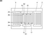
図1は、本発明の第1の実施形態に係る弾性波装置の平面図である。図2は、図1中のI-I線に沿う断面図である。図1においては、後述する第2の部分をハッチングにより示す。なお、図1以外の各平面図においても同様とする。 FIG. 1 is a plan view of an elastic wave device according to a first embodiment of the present invention. FIG. 2 is a sectional view taken along the line II in FIG. In FIG. 1, a second portion described later is shown by hatching. The same applies to each plan view other than FIG.
図1に示すように、弾性波装置1は圧電性基板2を有する。圧電性基板2は、本実施形態では圧電体層のみからなる圧電基板である。圧電性基板2には、適宜の圧電単結晶や圧電セラミックを用いることができる。より具体的には、圧電性基板2の材料として、例えば、ニオブ酸リチウム、タンタル酸リチウム、酸化亜鉛、窒化アルミニウム、水晶(SiO2)、またはサファイアなどを用いることができる。もっとも、圧電性基板2は圧電体層を含む積層体であってもよい。
As shown in FIG. 1, the
圧電性基板2上には、IDT電極3が設けられている。IDT電極3に交流電圧を印加することにより、弾性波が励振される。圧電性基板2上における、IDT電極3の弾性波伝搬方向両側には、一対の反射器4及び反射器5が設けられている。このように、本実施形態の弾性波装置1は弾性波共振子である。もっとも、本発明に係る弾性波装置1は、弾性波共振子を含むフィルタ装置などであってもよい。
IDT電極3は、第1の櫛歯状電極6及び第2の櫛歯状電極7を有する。第1の櫛歯状電極6は、第1のバスバー14と、第1のバスバー14にそれぞれ一端が接続された複数の第1の電極指16とを有する。第2の櫛歯状電極7は、第2のバスバー15と、第2のバスバー15にそれぞれ一端が接続された複数の第2の電極指17とを有する。複数の第1の電極指16と複数の第2の電極指17とは互いに間挿し合っている。複数の第1の電極指16は、第1のギャップG1を隔てて第2の櫛歯状電極7に対向している。複数の第2の電極指17は、第2のギャップG2を隔てて第1の櫛歯状電極6に対向している。
The
第1の櫛歯状電極6は、第1のバスバー14にそれぞれ一端が接続されており、複数の第2の電極指17に第2のギャップG2を隔てて対向している複数の第1のダミー電極指18を有する。第2の櫛歯状電極7は、第2のバスバー15にそれぞれ一端が接続されており、複数の第1の電極指16に第1のギャップG1を隔てて対向している複数の第2のダミー電極指19を有する。
One end of each of the first comb-teeth-shaped
ここで、複数の第1の電極指16及び第2の櫛歯状電極7は、第1のギャップG1を隔てて互いに対向する部分である第1の対向部をそれぞれ有する。複数の第1の電極指16の第1の対向部は、複数の第1の電極指16の先端部である。第2の櫛歯状電極7の第1の対向部は、本実施形態においては複数の第2のダミー電極指19の先端部である。
Here, the plurality of
同様に、複数の第2の電極指17及び第1の櫛歯状電極6は、第2のギャップG2を隔てて互いに対向する部分である第2の対向部をそれぞれ有する。複数の第2の電極指17の第2の対向部は、複数の第2の電極指17の先端部である。第1の櫛歯状電極6の第2の対向部は、本実施形態においては複数の第1のダミー電極指18の先端部である。なお、IDT電極3は、必ずしも第1のダミー電極指18及び第2のダミー電極指19を有していなくともよい。
Similarly, the plurality of
第1の櫛歯状電極6及び第2の櫛歯状電極7は、それぞれ主電極層を有する。本明細書において主電極層とは、50重量%以上を占める電極層をいう。図2に示すように、IDT電極3は、第1の金属により主電極層8が構成されている第1の部分Aと、第2の金属により主電極層9が構成されている第2の部分Bとを有する。より具体的には、図1に示すように、IDT電極3の第2の部分Bは、複数の第1の電極指16、複数の第2の電極指17、複数の第1のダミー電極指18及び複数の第2のダミー電極指19のそれぞれの先端部である。このように、本実施形態では、複数の第1の電極指16の第1の対向部及び第2の櫛歯状電極7の第1の対向部のうち両方と、複数の第2の電極指17の第2の対向部及び第1の櫛歯状電極6の第2の対向部のうち両方とが第2の部分Bである。
The first comb-
なお、複数の第1の電極指16の第1の対向部及び第2の櫛歯状電極7の第1の対向部のうち少なくとも一方と、複数の第2の電極指17の第2の対向部及び第1の櫛歯状電極6の第2の対向部のうち少なくとも一方とが第2の部分Bであればよい。あるいは、複数の第1の電極指16の第1の対向部、第2の櫛歯状電極7の第1の対向部、複数の第2の電極指17の第2の対向部及び第1の櫛歯状電極6の第2の対向部のうち少なくともいずれかの対向部が第2の部分Bであればよい。
Note that at least one of the first facing portions of the plurality of
他方、IDT電極3における第2の部分B以外の部分が第1の部分Aである。より具体的には、本実施形態では、複数の第1の電極指16、複数の第2の電極指17、複数の第1のダミー電極指18及び複数の第2のダミー電極指19のそれぞれの先端部以外の部分並びに第1のバスバー14及び第2のバスバー15が第1の部分Aである。
On the other hand, the portion other than the second portion B of the
ところで、IDT電極3の第1のバスバー14上及び第2のバスバー15上には、他の素子などに接続される配線電極の電極層が設けられることがある。この配線電極の電極層と、本発明におけるIDT電極3の第1のバスバー14及び第2のバスバー15とは別個のものであることを指摘しておく。
By the way, on the
弾性波装置1においては、第2の金属の密度は第1の金属の密度よりも高く、かつ第2の金属のヤング率は第1の金属のヤング率よりも高い。なお、第1の金属及び第2の金属の関係は、第2の金属の密度が第1の金属の密度よりも高い関係及び第2の金属のヤング率が第1の金属のヤング率よりも高い関係のうち少なくとも一方の関係であればよい。より具体的には、例えば、第1の金属がAlである場合には、第2の金属としてはTi、Cu、Mo、Cr、Ru、W、Pt、Ta、Co、Ni、AuまたはMnなどのうちいずれかを選択することができる。もっとも、第1の金属及び第2の金属は合金であってもよい。
In the
IDT電極3は、例えば、スパッタリング法または真空蒸着法などにより形成することができる。第1の部分Aを形成した後に第2の部分Bを形成してもよく、第2の部分Bを形成した後に第1の部分Aを形成してもよい。
The
本実施形態では、IDT電極3の第1の部分A及び第2の部分Bはそれぞれ単層の金属層からなる。反射器4及び反射器5も同様に単層の金属層からなる。なお、IDT電極3の第1の部分A及び第2の部分B並びに反射器4及び反射器5は、複数の金属層が積層された積層金属膜からなっていてもよい。
In this embodiment, the first portion A and the second portion B of the
本実施形態の特徴は、以下の構成を有することにある。1)IDT電極3が、第1の金属により主電極層が構成されている第1の部分Aと、第2の金属により主電極層が構成されている第2の部分Bとを有すること。2)複数の第1の電極指16の第1の対向部及び第2の櫛歯状電極7の第1の対向部のうち少なくとも一方と、複数の第2の電極指17の第2の対向部及び第1の櫛歯状電極6の第2の対向部のうち少なくとも一方とが第2の部分Bであること。3)IDT電極3における第2の部分B以外の部分が第1の部分Aであること。4)第1の金属及び第2の金属の関係が、第2の金属の密度が第1の金属の密度よりも高い関係及び第2の金属のヤング率が第1の金属のヤング率よりも高い関係のうち少なくとも一方の関係であること。それによって、IMDを効果的に抑制することができる。これを以下において説明する。
The feature of this embodiment is that it has the following configuration. 1) The
IMDの信号のうち2次非線形信号は、主に、IDT電極3における第1のギャップG1及び第2のギャップG2において生じる。本実施形態では、IDT電極3自体が互いに異なる金属により構成された第1の部分A及び第2の部分Bを有する。第1の部分Aと、第2の部分Bとは、連続的に形成されており、電気的に接続されている。IDT電極3における上記各ギャップを隔てて対向する第1の対向部及び第2の対向部が、第1の金属及び第2の金属のうちより重くまたはよりヤング率が高い第2の金属により主電極層9が構成された、第2の部分Bである。すなわち、IDT電極3における上記各ギャップに接する領域において、重い、またはヤング率の高い第2の金属が、圧電性基板2上に直接的に配置されている。このように、上記各ギャップに接する領域において、重い、またはヤング率の高い第2の金属を、圧電性基板2に近い位置に配置することによって、上記各ギャップにおける歪みを効果的に抑制することができ、2次非線形信号を効果的に抑制することができる。従って、IMDを効果的に抑制することができる。
The second-order nonlinear signal of the IMD signals mainly occurs in the first gap G1 and the second gap G2 in the
本実施形態のように、複数の第1の電極指16の第1の対向部及び第2の櫛歯状電極7の第1の対向部のうち両方と、複数の第2の電極指17の第2の対向部及び第1の櫛歯状電極6の第2の対向部のうち両方とが第2の部分Bであることが好ましい。それによって、第1のギャップG1及び第2のギャップG2における歪みをより一層抑制することができ、IMDをより一層抑制することができる。
As in the present embodiment, both of the first facing portions of the plurality of
下記の図3及び図4を参照して、第1の実施形態と第2の部分の配置が異なる、第1の実施形態の第1の変形例及び第2の変形例を示す。より具体的には、第1の変形例及び第2の変形例では、複数の第1の電極指の第1の対向部及び第2の櫛歯状電極の第1の対向部のうち一方と、複数の第2の電極指の第2の対向部及び第1の櫛歯状電極の第2の対向部のうち一方とが第2の部分である。第1の変形例及び第2の変形例においても、第1のギャップ及び第2のギャップにおける歪みを効果的に抑制することができ、IMDを効果的に抑制することができる。 With reference to FIG. 3 and FIG. 4 below, a first modification example and a second modification example of the first embodiment, in which the arrangement of the second portion is different, are shown. More specifically, in the first modified example and the second modified example, one of the first facing portions of the plurality of first electrode fingers and the first facing portion of the second comb-teeth-shaped electrode is provided. , One of the second facing portions of the plurality of second electrode fingers and the second facing portion of the first comb-shaped electrode is a second portion. Also in the first modified example and the second modified example, distortion in the first gap and the second gap can be effectively suppressed, and IMD can be effectively suppressed.
図3は、第1の実施形態の第1の変形例に係る弾性波装置の平面図である。図4は、第1の実施形態の第2の変形例に係る弾性波装置の平面図である。 FIG. 3 is a plan view of an elastic wave device according to a first modified example of the first embodiment. FIG. 4 is a plan view of an elastic wave device according to a second modification of the first embodiment.
図3に示すように、第1の変形例においては、第2の部分B1は、複数の第1の電極指16の先端部及び複数の第2の電極指17の先端部である。第1の部分A1は、複数の第1の電極指16及び複数の第2の電極指17のそれぞれの先端部以外の部分並びに複数の第1のダミー電極指28、複数の第2のダミー電極指29、第1のバスバー14及び第2のバスバー15である。もっとも、複数の第1の電極指16の先端部及び複数の第2の電極指17の先端部のうち少なくとも一方が第2の部分B1であってもよい。
As shown in FIG. 3, in the first modification, the second portion B1 is the tip portions of the plurality of
図4に示すように、第2の変形例においては、第2の部分B2は、複数の第1のダミー電極指18の先端部及び複数の第2のダミー電極指19の先端部である。第1の部分A2は、複数の第1のダミー電極指18及び複数の第2のダミー電極指19のそれぞれの先端部以外の部分並びに複数の第1の電極指26、複数の第2の電極指27、第1のバスバー14及び第2のバスバー15である。
As shown in FIG. 4, in the second modified example, the second portions B2 are the tip portions of the plurality of first
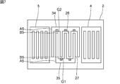
上述したように、IDT電極は第1のダミー電極指及び第2のダミー電極指を有していなくともよい。以下において、第1のダミー電極指及び第2のダミー電極指を有しない、第1の実施形態の第3~第5の変形例を示す。第3~第5の変形例においても、第1のギャップ及び第2のギャップにおける歪みを効果的に抑制することができ、IMDを効果的に抑制することができる。 As described above, the IDT electrode does not have to have the first dummy electrode finger and the second dummy electrode finger. In the following, third to fifth modified examples of the first embodiment, which do not have the first dummy electrode finger and the second dummy electrode finger, will be shown. Also in the third to fifth modified examples, distortion in the first gap and the second gap can be effectively suppressed, and IMD can be effectively suppressed.
図5に示すように、第3の変形例においては、複数の第1の電極指16及び第2のバスバー35が、第1のギャップG1を隔てて対向している。このように、本変形例では、第2の櫛歯状電極37の第1の対向部は、第2のバスバー35の各第1の電極指16に対向している部分である。複数の第1の電極指16の第1の対向部は、複数の第1の電極指16の先端部である。
As shown in FIG. 5, in the third modification, the plurality of
同様に、複数の第2の電極指17及び第1のバスバー34が、第2のギャップG2を隔てて対向している。このように、本変形例では、第1の櫛歯状電極36の第2の対向部は、第1のバスバー34の各第2の電極指17に対向している部分である。複数の第2の電極指17の第2の対向部は、複数の第2の電極指17の先端部である。下記の第4の変形例及び第5の変形例においても、各第1の対向部及び各第2の対向部は本変形例と同様である。
Similarly, the plurality of
本変形例においては、複数の第1の電極指16の第1の対向部及び第2の櫛歯状電極37の第1の対向部のうち両方と、複数の第2の電極指17の第2の対向部及び第1の櫛歯状電極36の第2の対向部のうち両方とが第2の部分B3である。他方、複数の第1の電極指16及び複数の第2の電極指17のそれぞれの先端部以外の部分が第1の部分A3である。さらに、第1のバスバー34の各第2の電極指17に対向している部分以外の部分及び第2のバスバー35の各第1の電極指16に対向している部分以外の部分も第1の部分A3である。
In the present modification, both of the first facing portions of the plurality of
図6に示すように、第4の変形例においては、第2の部分B4は、複数の第1の電極指16の先端部及び複数の第2の電極指17の先端部である。第1の部分A4は、複数の第1の電極指16及び複数の第2の電極指17のそれぞれの先端部以外の部分並びに第1のバスバー14及び第2のバスバー15である。
As shown in FIG. 6, in the fourth modification, the second portion B4 is the tip portions of the plurality of
図7に示すように、第5の変形例においては、第1のバスバー34の各第2の電極指27に対向している部分と、第2のバスバー35の各第1の電極指26に対向している部分とが第2の部分B5である。他方、複数の第1の電極指26及び複数の第2の電極指27が第1の部分A5である。さらに、第1のバスバー34の各第2の電極指27に対向している部分以外の部分及び第2のバスバー35の各第1の電極指26に対向している部分以外の部分も第1の部分A5である。
As shown in FIG. 7, in the fifth modification, a portion of the
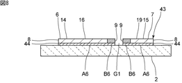
図2に示すように、第1の実施形態においては、IDT電極3は単層の金属層からなる。なお、IDT電極3は、主電極層以外の層を有していてもよい。図8に示す第1の実施形態の第6の変形例においては、IDT電極43は、第1の部分A6の主電極層8及び第2の部分B6の主電極層9と、圧電性基板2との間に設けられている密着層44を有する。それによって、IDT電極43と圧電性基板2との密着性をより確実に高めることができる。本変形例においても、IDT電極3における各ギャップに接する領域において、重い、またはヤング率の高い第2の金属が、圧電性基板2に近い位置に配置されているので、第1の実施形態と同様に、第1のギャップG1及び第2のギャップにおける歪みを効果的に抑制することができ、IMDを効果的に抑制することができる。
As shown in FIG. 2, in the first embodiment, the
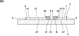
上述したように、第2の部分の主電極層は第2の金属により構成されている。ここで、第2の金属により構成される金属層は、第1の部分に至っていてもよい。図9に示す第1の実施形態の第7の変形例においては、第2の部分Bから第1の部分A7の主電極層8上に、第2の金属からなる金属層49が至っている。第1の部分A7に至っている上記金属層49は、第2の部分Bの主電極層9と一体として設けられている。なお、第1の部分A7から第2の部分Bの主電極層9上に、第1の金属からなる金属層が至っていてもよい。
As described above, the main electrode layer of the second portion is composed of the second metal. Here, the metal layer composed of the second metal may reach the first portion. In the seventh modified example of the first embodiment shown in FIG. 9, the
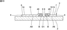
他方、図10に示す第1の実施形態の第8の変形例においては、第2の部分Bから第1の部分A8の主電極層8と圧電性基板2との間に、第2の金属からなる金属層49が至っている。第1の部分A8に至っている上記金属層49は、第2の部分Bの主電極層9と一体として設けられている。
On the other hand, in the eighth modified example of the first embodiment shown in FIG. 10, the second metal is provided between the
第7の変形例及び第8の変形例においても、第1の実施形態と同様に、第1のギャップG1及び第2のギャップにおける歪みを効果的に抑制することができ、IMDを効果的に抑制することができる。 Also in the seventh modified example and the eighth modified example, similarly to the first embodiment, the strain in the first gap G1 and the second gap can be effectively suppressed, and the IMD can be effectively performed. Can be suppressed.
1…弾性波装置
2…圧電性基板
3…IDT電極
4…反射器
5…反射器
6…第1の櫛歯状電極
7…第2の櫛歯状電極
8…主電極層
9…主電極層
14…第1のバスバー
15…第2のバスバー
16…第1の電極指
17…第2の電極指
18…第1のダミー電極指
19…第2のダミー電極指
26…第1の電極指
27…第2の電極指
28…第1のダミー電極指
29…第2のダミー電極指
34…第1のバスバー
35…第2のバスバー
36…第1の櫛歯状電極
37…第2の櫛歯状電極
43…IDT電極
44…密着層
49…金属層
A,A1~A8…第1の部分
B,B1~B6…第2の部分
DESCRIPTION OF
Claims (7)
前記圧電性基板上に設けられているIDT電極と、
を備え、
前記IDT電極が、それぞれ主電極層を含む第1の櫛歯状電極及び第2の櫛歯状電極を有し、
前記第1の櫛歯状電極が、第1のバスバーと、前記第1のバスバーに一端が接続された複数の第1の電極指と、を有し、前記第2の櫛歯状電極が、第2のバスバーと、前記第2のバスバーに一端が接続されており、かつ前記複数の第1の電極指と間挿し合っている複数の第2の電極指と、を有し、
前記IDT電極が、第1の金属により前記主電極層が構成されている第1の部分と、第2の金属により前記主電極層が構成されている第2の部分と、を有し、
前記複数の第1の電極指及び前記第2の櫛歯状電極が、ギャップを隔てて互いに対向する部分である第1の対向部をそれぞれ有し、前記複数の第2の電極指及び前記第1の櫛歯状電極が、ギャップを隔てて互いに対向する部分である第2の対向部をそれぞれ有し、
前記複数の第1の電極指の前記第1の対向部、前記第2の櫛歯状電極の前記第1の対向部、前記複数の第2の電極指の前記第2の対向部及び前記第1の櫛歯状電極の前記第2の対向部のうち、少なくともいずれかの対向部が前記第2の部分であり、前記IDT電極における前記第2の部分以外の部分が前記第1の部分であり、
前記第2の金属の密度が前記第1の金属の密度よりも高い、弾性波装置。 A piezoelectric substrate,
An IDT electrode provided on the piezoelectric substrate,
Equipped with
The IDT electrode has a first comb-shaped electrode and a second comb-shaped electrode, each of which includes a main electrode layer,
The first comb tooth-shaped electrode has a first bus bar and a plurality of first electrode fingers whose one end is connected to the first bus bar, and the second comb tooth-shaped electrode is A second bus bar and a plurality of second electrode fingers, one end of which is connected to the second bus bar, and which are interleaved with the plurality of first electrode fingers,
The IDT electrode has a first portion in which the main electrode layer is made of a first metal and a second portion in which the main electrode layer is made of a second metal,
The plurality of first electrode fingers and the second comb-teeth-shaped electrodes each have a first facing portion that is a portion facing each other with a gap, and the plurality of second electrode fingers and the plurality of second electrode fingers are provided. One comb-tooth electrode has second facing portions that are portions facing each other across a gap,
The first facing portion of the plurality of first electrode fingers, the first facing portion of the second comb-shaped electrode, the second facing portion of the plurality of second electrode fingers, and the first facing portion of the plurality of second electrode fingers. At least one of the second facing portions of the one comb-teeth-shaped electrode is the second portion, and a portion of the IDT electrode other than the second portion is the first portion. Yes,
The acoustic wave device, wherein the density of the second metal is higher than the density of the first metal.
前記圧電性基板上に設けられているIDT電極と、
を備え、
前記IDT電極が、それぞれ主電極層を含む第1の櫛歯状電極及び第2の櫛歯状電極を有し、
前記第1の櫛歯状電極が、第1のバスバーと、前記第1のバスバーに一端が接続された複数の第1の電極指と、を有し、前記第2の櫛歯状電極が、第2のバスバーと、前記第2のバスバーに一端が接続されており、かつ前記複数の第1の電極指と間挿し合っている複数の第2の電極指と、を有し、
前記IDT電極が、第1の金属により前記主電極層が構成されている第1の部分と、第2の金属により前記主電極層が構成されている第2の部分と、を有し、
前記複数の第1の電極指及び前記第2の櫛歯状電極が、ギャップを隔てて互いに対向する部分である第1の対向部をそれぞれ有し、前記複数の第2の電極指及び前記第1の櫛歯状電極が、ギャップを隔てて互いに対向する部分である第2の対向部をそれぞれ有し、
前記複数の第1の電極指の前記第1の対向部、前記第2の櫛歯状電極の前記第1の対向部、前記複数の第2の電極指の前記第2の対向部及び前記第1の櫛歯状電極の前記第2の対向部のうち、少なくともいずれかの対向部が前記第2の部分であり、前記IDT電極における前記第2の部分以外の部分が前記第1の部分であり、
前記第2の金属のヤング率が前記第1の金属のヤング率よりも高い、弾性波装置。 A piezoelectric substrate,
An IDT electrode provided on the piezoelectric substrate,
Equipped with
The IDT electrode has a first comb-shaped electrode and a second comb-shaped electrode, each of which includes a main electrode layer,
The first comb tooth-shaped electrode has a first bus bar and a plurality of first electrode fingers whose one end is connected to the first bus bar, and the second comb tooth-shaped electrode is A second bus bar and a plurality of second electrode fingers, one end of which is connected to the second bus bar, and which are interleaved with the plurality of first electrode fingers,
The IDT electrode has a first portion in which the main electrode layer is made of a first metal and a second portion in which the main electrode layer is made of a second metal,
The plurality of first electrode fingers and the second comb-teeth-shaped electrodes each have a first facing portion that is a portion facing each other with a gap, and the plurality of second electrode fingers and the plurality of second electrode fingers are provided. 1 comb-teeth-shaped electrode has a second facing portion that is a portion facing each other across a gap,
The first facing portion of the plurality of first electrode fingers, the first facing portion of the second comb-shaped electrode, the second facing portion of the plurality of second electrode fingers, and the first facing portion of the plurality of second electrode fingers. At least one of the second facing portions of the one comb-teeth-shaped electrode is the second portion, and a portion of the IDT electrode other than the second portion is the first portion. Yes,
An elastic wave device in which the Young's modulus of the second metal is higher than the Young's modulus of the first metal.
Priority Applications (2)
| Application Number | Priority Date | Filing Date | Title |
|---|---|---|---|
| CN201980081989.4A CN113196656B (en) | 2018-12-13 | 2019-10-28 | Elastic wave device |
| US17/326,385 US11811388B2 (en) | 2018-12-13 | 2021-05-21 | Acoustic wave device |
Applications Claiming Priority (2)
| Application Number | Priority Date | Filing Date | Title |
|---|---|---|---|
| JP2018-233247 | 2018-12-13 | ||
| JP2018233247 | 2018-12-13 |
Related Child Applications (1)
| Application Number | Title | Priority Date | Filing Date |
|---|---|---|---|
| US17/326,385 Continuation US11811388B2 (en) | 2018-12-13 | 2021-05-21 | Acoustic wave device |
Publications (1)
| Publication Number | Publication Date |
|---|---|
| WO2020121663A1 true WO2020121663A1 (en) | 2020-06-18 |
Family
ID=71077167
Family Applications (1)
| Application Number | Title | Priority Date | Filing Date |
|---|---|---|---|
| PCT/JP2019/042190 Ceased WO2020121663A1 (en) | 2018-12-13 | 2019-10-28 | Elastic wave device |
Country Status (3)
| Country | Link |
|---|---|
| US (1) | US11811388B2 (en) |
| CN (1) | CN113196656B (en) |
| WO (1) | WO2020121663A1 (en) |
Families Citing this family (4)
| Publication number | Priority date | Publication date | Assignee | Title |
|---|---|---|---|---|
| CN113508495B (en) * | 2019-03-06 | 2022-07-19 | 株式会社村田制作所 | Filter, multiplexer, high-frequency front-end circuit, and communication device |
| CN114553173A (en) * | 2022-02-23 | 2022-05-27 | 广东广纳芯科技有限公司 | TC-SAW device and its manufacturing method |
| CN114866062B (en) * | 2022-04-19 | 2025-01-10 | 天通瑞宏科技有限公司 | A surface acoustic wave resonator |
| CN115001437A (en) * | 2022-06-14 | 2022-09-02 | 天通瑞宏科技有限公司 | Surface acoustic wave resonator and filter |
Citations (3)
| Publication number | Priority date | Publication date | Assignee | Title |
|---|---|---|---|---|
| JP2007235711A (en) * | 2006-03-02 | 2007-09-13 | Murata Mfg Co Ltd | Surface acoustic wave apparatus |
| JP2017228945A (en) * | 2016-06-22 | 2017-12-28 | 太陽誘電株式会社 | Acoustic wave resonator, filter and multiplexer |
| WO2018131454A1 (en) * | 2017-01-13 | 2018-07-19 | 株式会社村田製作所 | Elastic wave device |
Family Cites Families (8)
| Publication number | Priority date | Publication date | Assignee | Title |
|---|---|---|---|---|
| JP3498215B2 (en) | 2001-04-09 | 2004-02-16 | 株式会社村田製作所 | Surface acoustic wave filter, surface acoustic wave device, and communication device |
| US8669832B2 (en) * | 2009-02-25 | 2014-03-11 | Panasonic Corporation | Acoustic wave device and acoustic wave filter |
| CN102823130B (en) * | 2010-05-13 | 2014-12-10 | 株式会社村田制作所 | Acoustic wave device |
| CN205725680U (en) * | 2013-12-26 | 2016-11-23 | 株式会社村田制作所 | Acoustic wave device |
| WO2016111315A1 (en) * | 2015-01-07 | 2016-07-14 | 株式会社村田製作所 | Acoustic wave device |
| US10361678B2 (en) * | 2015-12-14 | 2019-07-23 | Taiyo Yuden Co., Ltd. | Acoustic wave resonator, filter, and duplexer |
| JP6465065B2 (en) * | 2016-04-25 | 2019-02-06 | 株式会社村田製作所 | Elastic wave device |
| WO2017187724A1 (en) * | 2016-04-27 | 2017-11-02 | 株式会社村田製作所 | Elastic wave device |
-
2019
- 2019-10-28 WO PCT/JP2019/042190 patent/WO2020121663A1/en not_active Ceased
- 2019-10-28 CN CN201980081989.4A patent/CN113196656B/en active Active
-
2021
- 2021-05-21 US US17/326,385 patent/US11811388B2/en active Active
Patent Citations (3)
| Publication number | Priority date | Publication date | Assignee | Title |
|---|---|---|---|---|
| JP2007235711A (en) * | 2006-03-02 | 2007-09-13 | Murata Mfg Co Ltd | Surface acoustic wave apparatus |
| JP2017228945A (en) * | 2016-06-22 | 2017-12-28 | 太陽誘電株式会社 | Acoustic wave resonator, filter and multiplexer |
| WO2018131454A1 (en) * | 2017-01-13 | 2018-07-19 | 株式会社村田製作所 | Elastic wave device |
Also Published As
| Publication number | Publication date |
|---|---|
| US20210328572A1 (en) | 2021-10-21 |
| CN113196656A (en) | 2021-07-30 |
| CN113196656B (en) | 2024-07-05 |
| US11811388B2 (en) | 2023-11-07 |
Similar Documents
| Publication | Publication Date | Title |
|---|---|---|
| US10425058B2 (en) | Elastic wave device | |
| CN113196656B (en) | Elastic wave device | |
| CN105531926B (en) | Elastic wave resonator, acoustic wave filter device and duplexer | |
| JP2022126852A (en) | Elastic surface wave element | |
| JP6888691B2 (en) | Elastic wave device | |
| JP6813108B2 (en) | Elastic wave device | |
| WO2018225650A1 (en) | Elastic wave filter device, multiplexer, and compound filter device | |
| CN103250348A (en) | Surface acoustic wave device | |
| US11863155B2 (en) | Surface acoustic wave element | |
| WO2006109591A1 (en) | Elastic wave element | |
| CN113872562A (en) | Surface acoustic wave device | |
| JP5083469B2 (en) | Surface acoustic wave device | |
| CN114430886A (en) | Elastic wave device | |
| JPWO2008035546A1 (en) | Boundary acoustic wave device | |
| JP7544147B2 (en) | Elastic wave device and ladder type filter | |
| JP7168009B2 (en) | Acoustic wave devices and multiplexers | |
| JP2013201468A (en) | Acoustic wave element and acoustic wave device using the same | |
| JP6276354B2 (en) | Interdigital transducer | |
| CN115777176A (en) | Elastic wave device | |
| JP4507819B2 (en) | Surface acoustic wave device | |
| WO2023162979A1 (en) | Elastic wave device | |
| WO2012026207A1 (en) | Elastic wave filter | |
| JP2012129938A (en) | Elastic wave device |
Legal Events
| Date | Code | Title | Description |
|---|---|---|---|
| 121 | Ep: the epo has been informed by wipo that ep was designated in this application |
Ref document number: 19897097 Country of ref document: EP Kind code of ref document: A1 |
|
| NENP | Non-entry into the national phase |
Ref country code: DE |
|
| 122 | Ep: pct application non-entry in european phase |
Ref document number: 19897097 Country of ref document: EP Kind code of ref document: A1 |
|
| NENP | Non-entry into the national phase |
Ref country code: JP |