WO2020110867A1 - 電気素子搭載用アレイパッケージおよび電気装置 - Google Patents
電気素子搭載用アレイパッケージおよび電気装置 Download PDFInfo
- Publication number
- WO2020110867A1 WO2020110867A1 PCT/JP2019/045514 JP2019045514W WO2020110867A1 WO 2020110867 A1 WO2020110867 A1 WO 2020110867A1 JP 2019045514 W JP2019045514 W JP 2019045514W WO 2020110867 A1 WO2020110867 A1 WO 2020110867A1
- Authority
- WO
- WIPO (PCT)
- Prior art keywords
- light emitting
- element mounting
- emitting element
- packages
- package
- Prior art date
- Legal status (The legal status is an assumption and is not a legal conclusion. Google has not performed a legal analysis and makes no representation as to the accuracy of the status listed.)
- Ceased
Links
Images










Classifications
-
- H—ELECTRICITY
- H01—ELECTRIC ELEMENTS
- H01S—DEVICES USING THE PROCESS OF LIGHT AMPLIFICATION BY STIMULATED EMISSION OF RADIATION [LASER] TO AMPLIFY OR GENERATE LIGHT; DEVICES USING STIMULATED EMISSION OF ELECTROMAGNETIC RADIATION IN WAVE RANGES OTHER THAN OPTICAL
- H01S5/00—Semiconductor lasers
- H01S5/02—Structural details or components not essential to laser action
- H01S5/022—Mountings; Housings
-
- H—ELECTRICITY
- H10—SEMICONDUCTOR DEVICES; ELECTRIC SOLID-STATE DEVICES NOT OTHERWISE PROVIDED FOR
- H10H—INORGANIC LIGHT-EMITTING SEMICONDUCTOR DEVICES HAVING POTENTIAL BARRIERS
- H10H20/00—Individual inorganic light-emitting semiconductor devices having potential barriers, e.g. light-emitting diodes [LED]
- H10H20/80—Constructional details
- H10H20/85—Packages
-
- H—ELECTRICITY
- H10—SEMICONDUCTOR DEVICES; ELECTRIC SOLID-STATE DEVICES NOT OTHERWISE PROVIDED FOR
- H10H—INORGANIC LIGHT-EMITTING SEMICONDUCTOR DEVICES HAVING POTENTIAL BARRIERS
- H10H20/00—Individual inorganic light-emitting semiconductor devices having potential barriers, e.g. light-emitting diodes [LED]
- H10H20/80—Constructional details
- H10H20/85—Packages
- H10H20/857—Interconnections, e.g. lead-frames, bond wires or solder balls
-
- H—ELECTRICITY
- H10—SEMICONDUCTOR DEVICES; ELECTRIC SOLID-STATE DEVICES NOT OTHERWISE PROVIDED FOR
- H10H—INORGANIC LIGHT-EMITTING SEMICONDUCTOR DEVICES HAVING POTENTIAL BARRIERS
- H10H20/00—Individual inorganic light-emitting semiconductor devices having potential barriers, e.g. light-emitting diodes [LED]
- H10H20/80—Constructional details
- H10H20/85—Packages
- H10H20/858—Means for heat extraction or cooling
Definitions
- the disclosed embodiments relate to an array package for mounting an electric element and an electric device.
- Patent Document 1 a light emitting device in which a plurality of light emitting elements are arranged in a matrix on a substrate is known (for example, see Patent Document 1).
- An electric element mounting array package is provided with a plurality of electric element mounting packages having electric element mounting surfaces arranged side by side, and the height of the mounting surface of at least one electric element mounting package. However, it is different from the height of the mounting surface of the other electric element mounting package.
- An electric device includes the electric element mounting array package described above, and a plurality of electric elements mounted on the mounting surfaces of the plurality of electric element mounting packages, respectively. ..
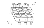
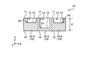
- FIG. 1A is a perspective view of a light emitting device mounting array package according to an embodiment. 1B is a sectional view taken along the line AA shown in FIG. 1A.
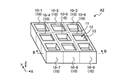
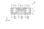
- FIG. 2A is a perspective view of a light emitting element mounting array package according to another aspect 1 of the embodiment. 2B is a sectional view taken along the line BB shown in FIG. 2A.
- FIG. 3 is a perspective view of a light emitting element mounting array package according to another aspect 2 of the embodiment.
- FIG. 4A is a perspective view of a light emitting element mounting array package according to another aspect 3 of the embodiment. 4B is a cross-sectional view taken along the line CC of FIG. 4A.
- FIG. 5A is a perspective view of a light emitting device mounting array package according to another aspect 4 of the embodiment.
- 5B is a sectional view taken along the line DD of FIG. 5A.
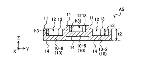
- 5C is a cross-sectional view taken along the line EE shown in FIG. 5A.
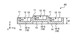
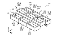
- FIG. 6A is a perspective view of a light emitting element mounting array package according to another aspect 5 of the embodiment.
- FIG. 6B is a sectional view taken along line FF shown in FIG. 6A.
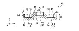
- FIG. 6C is a sectional view taken along line GG shown in FIG. 6A.
- FIG. 7A is a perspective view of a light emitting element mounting array package according to another aspect 6 of the embodiment. 7B is a cross-sectional view taken along line HH shown in FIG. 7A.
- FIG. 10A is a perspective view of a light emitting device mounting array package according to another aspect 9 of the embodiment.
- FIG. 10B is a sectional view taken along line NN shown in FIG. 10A.
- FIG. 10C is a sectional view taken along line OO shown in FIG. 10A.
- FIG. 11A is a perspective view of a light emitting device mounting array package according to another aspect 10 of the embodiment. 11B is a cross-sectional view taken along the line PP of FIG. 11A.
- FIG. 11C is a sectional view taken along line QQ shown in FIG. 11A.
- FIG. 12A is a perspective view of a light emitting element mounting array package according to another aspect 11 of the embodiment. 12B is a cross-sectional view taken along the line RR shown in FIG.
- FIG. 13 is a plan view showing one manufacturing process of the light emitting element mounting substrate according to the embodiment.
- FIG. 14 is a cross-sectional view showing one manufacturing process of the light emitting element mounting substrate according to the embodiment.
- FIG. 15A is a perspective view of a light emitting element mounting array package in a reference example.
- FIG. 15B is a sectional view taken along line TT shown in FIG. 15A.
- FIG. 15C is a cross-sectional view taken along the line UU shown in FIG. 15A.
- an electric element mounting array package and an electric device disclosed in the present application will be described below with reference to the accompanying drawings.
- a mode in which a light emitting element is applied to an electric element hereinafter referred to as a light emitting element mounting array package and a light emitting device
- the invention is not limited to the light emitting element and can be applied to all electric elements having heat generation property.
- LSI Large Scale Integrated circuit
- CCD Charge Coupled Device
- Laser Diode Laser Diode
- LED Light emitting diode
- the embodiments described below are particularly useful for laser diodes.
- the light emitting element mounting array package A1 is provided with a plurality of light emitting element mounting packages 10 arranged side by side.
- a light emitting element mounting array package A1 nine rectangular parallelepiped light emitting element mounting packages 10-1 to 10-9 are arranged side by side in a matrix of 3 rows ⁇ 3 columns. ..
- Figure 3 illustrates a dimensional Cartesian coordinate system.
- a mounting surface 13 for mounting a light emitting element (not shown) is provided on the bottom of the recess 12 formed in the light emitting element mounting package 10.
- the light emitting element mounting package 10 has a back surface 14 on the opposite side of the front surface 11, and the back surfaces 14 of all the light emitting element mounting packages 10 are substantially flush. That is, all the light emitting element mounting packages 10 have the same thickness t1.
- the height of the mounting surface 13 of at least one light emitting element mounting package 10 is different from the height of the mounting surface 13 of another light emitting element mounting package 10.
- the height of the mounting surface 13 of the light emitting element mounting package 10-5 is different from that of the other light emitting element mounting packages 10-1 to 10-4, 10-6. It is lower than the height of the mounting surface 13 of 10-9.
- the depth h1 of the recess 12 of the light emitting element mounting package 10-5 is smaller than that of the other light emitting element mounting packages 10-1 to 10-4, 10-6 to 10-9. It is deeper than the depth h2 of the recess 12 (that is, h1>h2).
- the height of the mounting surface 13 of the light emitting element mounting package 10-5 arranged in the central portion is such that the light emitting element mounting packages 10-1 to 10-10 arranged in the peripheral portion. -4, different from the height of the mounting surface 13 of 10-6 to 10-9.
- the thermal interference from the adjacent light emitting elements can be reduced.
- the base and bank are integrally formed of ceramics. .. That is, the light emitting element mounting package 10 does not have an interface between the base and the bank portion, which is made of different materials and causes a large thermal resistance.
- the thermal resistance between the base and the bank can be reduced, so that heat can be efficiently transferred from the base to the bank. Therefore, according to the embodiment, it is possible to realize the light emitting element mounting array package A1 having high heat dissipation.
- the light emitting element mounting package 10 does not require a step of joining between the base and the bank portion, and also does not require a joining material such as solder. Therefore, according to the embodiment, it is possible to realize the light emitting element mounting array package A1 having a low manufacturing cost.
- all the light emitting element mounting packages 10 are integrally formed of ceramics. That is, the light emitting element mounting array package A1 is not provided with an interface between adjacent light emitting element mounting packages 10 that is made of different materials and causes a large thermal resistance.
- the thermal resistance between the adjacent light emitting element mounting packages 10 can be reduced, so that heat can be efficiently transmitted to the adjacent light emitting element mounting packages 10. Therefore, according to the embodiment, it is possible to realize the light emitting element mounting array package A1 having high heat dissipation.
- the light emitting element mounting array package A1 does not require a step of joining between the adjacent light emitting element mounting packages 10 and also a joining material such as solder. Therefore, according to the embodiment, it is possible to realize the light emitting element mounting array package A1 having a low manufacturing cost.
- the light emitting element mounting package 10 is made of ceramics. As such ceramics, for example, alumina, silica, mullite, cordierite, forsterite, aluminum nitride, silicon nitride, silicon carbide or glass ceramics is suitable.
- the light emitting element mounting package 10 is preferably made of ceramics containing aluminum nitride (AlN) as a main component because it has a high thermal conductivity and a thermal expansion coefficient close to that of the light emitting element.
- AlN aluminum nitride
- the light emitting element mounting package 10 may include aluminum nitride in an amount of 90 mass% or more. By setting the content of aluminum nitride to 90% by mass or more, the thermal conductivity of the light emitting device mounting package 10 can be 150 W/mK or more. Then, the light emitting element mounting array package A1 having excellent heat dissipation can be realized.
- the mounting surface 13 of the light emitting device mounting package 10 is provided with a pair of device terminals made of metal.
- a pair of power supply terminals are provided on the front surface 11 or the back surface 14 of the light emitting element mounting package 10.
- “composed of a metal” means that a part other than metal, for example, ceramics may be included, and the same applies below.
- the pair of element terminals are terminals that are respectively connected to the positive electrode and the negative electrode of the light emitting element.
- the pair of element terminals and each electrode of the light emitting element are connected by, for example, a conductive bonding material such as solder or a bonding wire.
- the pair of power supply terminals are terminals connected to an external power supply (not shown).
- an external power supply not shown.
- the pair of device terminals and the pair of power supply terminals penetrate in the Z-axis direction. They are connected by a pair of via conductors.
- the pair of element terminals, the pair of power terminals, and the pair of via conductors may be formed by a metallized film obtained by sintering metal powder. Since this metallized film can be adhered to the surface of the ceramics forming the light emitting device mounting package 10 with high strength, a highly reliable light emitting device mounting array package A1 can be realized.
- the pair of device terminals As a material for the pair of device terminals, the pair of power supply terminals, and the pair of via conductors, when aluminum nitride is applied to the light emitting device mounting package 10, simultaneous firing is possible. Any one of tungsten (W), molybdenum (Mo), an alloy thereof, or a metal material in which copper or the like is compounded is suitable.
- At least one of the device terminal and the power supply terminal may be provided on the upper surface of the bank (that is, the front surface 11).
- a plating film such as Ni may be formed on the surface of the metallized film that constitutes the pair of element terminals and the pair of power supply terminals. Further, solder or Au—Sn plating film may be provided on the surface of the plating film.
- the light emitting element mounting array package A2 shown in FIGS. 2A and 2B is another aspect 1 of the embodiment.
- the configuration of the recess 12 is different from that of the embodiment.
- the light emitting element mounting packages 10 having different recesses 12 having different depths are alternately arranged.
- the package 10-3 and the package 10-3 are arranged side by side in the X-axis direction.
- a package 10-4 for mounting a light emitting element in which the recess 12 has a depth h2 a package 10-5 for mounting a light emitting element in which the recess 12 has a depth h1
- the package 10-6 and the package 10-6 are arranged side by side in the X-axis direction.
- the light emitting element mounting package 10-7 having the recess 12 having the depth h1 the light emitting element mounting package 10-8 having the recess 12 having the depth h2, and the light emitting element mounting package having the recess 12 having the depth h1.
- the package 10-9 and the package 10-9 are arranged side by side in the X-axis direction.
- the height position where the temperature is high due to the heat generated from the mounted light emitting elements can be alternately changed in the direction parallel to the mounting surface 13. it can. Therefore, according to the other aspect 1, when a plurality of light emitting elements are arranged side by side, thermal interference from the adjacent light emitting elements can be further reduced.
- the light emitting element mounting packages 10 having different recesses 12 in different depths may be alternately arranged not only in the X-axis direction but also in the Y-axis direction. .. Accordingly, when a plurality of light emitting elements are arranged side by side in a matrix, it is possible to reduce thermal interference from adjacent light emitting elements.
- the light emitting element mounting array package A3 shown in FIG. 3 is another aspect 2 of the embodiment.
- the arrangement of the light emitting element mounting package 10 is different from that of the other aspect 1.
- light emitting element mounting packages 10 having different recesses 12 having different depths are arranged alternately in the horizontal direction.
- the light emitting element mounting package 10-1 having the recess 12 having the depth h2 and the light emitting element mounting package 10-2 having the recess 12 having the depth h1 are arranged side by side in the X-axis direction.
- the package 10-5 and the package 10-5 are arranged side by side in the X-axis direction.
- the light emitting element mounting package 10-6 having the recess 12 having the depth h1 and the light emitting element mounting package 10-7 having the recess 12 having the depth h2 are arranged side by side in the X-axis direction.
- the recess 12 of at least one light emitting element mounting package 10 is horizontally displaced from the recess 12 of the adjacent light emitting element mounting package 10.
- the recesses 12 of the light emitting device mounting packages 10-3 to 10-5 are different from the recesses 12 of the light emitting device mounting packages 10-1, 10-2, 10-6, 10-7 adjacent in the Y-axis direction.
- the sides of the recess 12 are arranged so as to be offset from each other in the X-axis direction.
- a plurality of light emitting element mounting packages 10 may be arranged in a staggered pattern.
- the plurality of light emitting element mounting packages 10 when they are arranged vertically and horizontally in a plane, they may be arranged in two rows in a zigzag pattern.
- the bank portion is not continuous for a long time, and therefore, the portion that does not emit light is not linear or striped. That is, according to the other aspect 2, the intensity of the place where the emitted light intensity is high and the place where the emitted light intensity is low are small, so that it is possible to realize a light emitting device with uniform brightness.
- the plurality of light emitting element mounting packages 10 in a zigzag manner, when the plurality of light emitting elements are arranged side by side, it is possible to widen all the intervals between the light emitting elements adjacent to each other. Therefore, according to the other aspect 2, when a plurality of light emitting elements are arranged side by side, the thermal interference from the adjacent light emitting elements can be further efficiently reduced.
- the light emitting element mounting array package A4 shown in FIGS. 4A and 4B is another aspect 3 of the embodiment.
- a plurality of (six in the figure) light emitting element mounting packages 10 having the recesses 12 having the same depth h3 and having the same thickness t2 are arranged differently from the embodiment.
- the height of the front surface 11 of at least one light emitting element mounting package 10 is different from the height of the front surface 11 of another light emitting element mounting package 10.
- the light emitting element mounting package 10-1 in which the front surface 11 is in a low position the light emitting element mounting package 10-2 in which the front surface 11 is in a high position, and the front surface 11 in a low position
- the light emitting element mounting package 10-4 in which the front surface 11 is at a high position
- the light emitting element mounting package 10-5 in which the front surface 11 is at a low position
- the front surface 11 is at a high position
- the height of the mounting surface 13 of the light emitting element mounting package 10-2, 10-4, 10-6 is made equal to that of the other light emitting element mounting package 10-1, 10-3, 10-5.
- the height of can be different.
- an exposed surface which is not in contact with the adjacent light emitting element mounting packages 10-1, 10-3, 10-5 can be provided on the side of the light emitting element mounting packages 10-2, 10-4, 10-6. ..
- the light emitting element mounting array package A4 having high heat dissipation can be realized.
- the height of one light emitting element mounting package 10 protruding from the other light emitting element mounting package 10 is preferably 10 or more when the height of the light emitting element mounting package 10 is 100. It may be 15 or more and 40 or less.
- the light emitting element mounting package 10-5 arranged in the central portion is arranged in the peripheral portion and the light emitting element mounting packages 10-1 to 10-4, 10-6 to 10-9 to Z are arranged. It projects in the axial direction.
- the light emitting element mounting package 10-5 arranged in the central portion projects in the Z axis positive direction.
- the central portion is located in the central portion in both the row direction and the column direction when the light emitting element mounting packages 10-5 are arranged in a plane.
- the height of the mounting surface 13 of the light emitting element mounting package 10-5 is different from the height of the mounting surface 13 of the other light emitting element mounting packages 10-1 to 10-4 and 10-6 to 10-9. Can be made. Further, an exposed surface which is not in contact with the adjacent light emitting element mounting packages 10-2, 10-4, 10-6, 10-8 can be provided on the side of the light emitting element mounting package 10-5.
- the thermal interference from the adjacent light emitting element can be further reduced. it can.
- 5A to 5C show an example in which the light emitting element mounting package 10-5 is projected in the Z axis positive direction, but the light emitting element mounting package 10-5 may be projected in the Z axis negative direction. Good.
- the light emitting element mounting array package A6 shown in FIGS. 6A to 6C is another aspect 5 of the embodiment.
- a plurality of the light emitting element mounting packages 10 arranged side by side in the row direction (that is, the X-axis direction) are mainly arranged.
- the height of the front surface 11 is different from the height of the front surface 11 of the plurality of light emitting element mounting packages 10 adjacent to each other in the column direction (that is, the Y-axis direction).
- the light emitting element mounting packages 10-4 to 10-6 with the front surface 11 at a high position are provided side by side in the X-axis direction.
- the light emitting element mounting packages 10-4 to 10-6 and the light emitting element mounting packages 10-7 to 10-9 which are adjacent to each other in the column direction and the light emitting element mounting packages 10-7 to 10-9 are
- the front surface 11 is provided at a low position.
- the front surface 11 of the light emitting element mounting packages 10-4 to 10-6 is provided with the adjacent light emitting element mounting packages 10-1 to 10-3, 10-7 to 10-. It may be provided at a position lower than the front surface 11 of the plate 9.
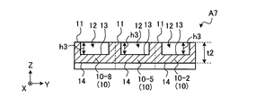
- the light emitting element mounting array package A7 shown in FIGS. 7A to 7C is another aspect 6 of the embodiment.
- the height of 11 is different from the height of the front surface 11 of the plurality of light emitting element mounting packages 10 adjacent in the row direction (X axis direction).
- the heights of the mounting surfaces 13 of the light emitting element mounting packages 10-2, 10-5, 10-8 are set so that the adjacent light emitting element mounting packages 10-1, 10-3, 10-4, 10-6.
- the height can be different from the height of the mounting surface 13 of 10-7, 10-9.
- the exposed surface not contacting the light emitting element mounting packages 10-1, 10-3, 10-4, 10-6, 10-7, 10-9 which are adjacent in the column direction has a light emitting element mounting package 10-2, It can be provided on the side of 10-5, 10-8.
- the front surface 11 of the light emitting element mounting packages 10-2, 10-5, and 10-8 is provided with the adjacent light emitting element mounting packages 10-1, 10-3, and 10-. It may be provided at a position lower than the front surface 11 of 4, 10-6, 10-7, 10-9.
- the light emitting element mounting packages 10-2, 10-4 to 10-6, 10-8 with the front surface 11 at a high position are provided in a cross shape.
- the light emitting device mounting packages 10-1 and 10-4 are provided adjacent to the light emitting device mounting packages 10-2, 10-4 to 10-6 and 10-8 and provided at the corners of the light emitting device mounting array package A8.
- -3, 10-7, and 10-9 are provided at positions where the front surface 11 is low.
- the heights of the mounting surfaces 13 of the light emitting element mounting packages 10-2, 10-4, 10-6, 10-8 are set to be equal to the adjacent light emitting element mounting packages 10-1, 10-3, 10-7.
- the height can be different from the height of the mounting surface 13 of 10-9.
- the exposed surface which is not in contact with the adjacent light emitting device mounting packages 10-1, 10-3, 10-7, 10-9 has light emitting device mounting packages 10-2, 10-4, 10-6, 10-8. Can be provided laterally.
- thermal interference from the adjacent light emitting elements is caused. Can be reduced.
- the front surface 11 of the light emitting element mounting package 10-2, 10-4 to 10-6, 10-8 is provided adjacent to the light emitting element mounting package 10-1, 10-. It may be provided at a position lower than the front surface 11 of 3, 10-7, 10-9.
- the front surface 11 of the light emitting element mounting package 10-1, 10-3, 10-5, 10-7, 10-9 is arranged adjacent to the light emitting element mounting package 10-.
- An example is shown in which they are arranged at a position higher than the front surface 11 of 2, 10-4, 10-6, 10-8.
- the light emitting element mounting packages 10-3, 10-5, 10-7 in which the front surface 11 is located at a high position are diagonally arranged. Then, the light emitting device mounting packages 10-3, 10-5, 10-7 adjacent to the light emitting device mounting packages 10-1, 10-2, 10-4, 10-6, 10-8, 10-9. Is provided at a position where the front surface 11 is low.
- the heights of the mounting surfaces 13 of the light emitting element mounting packages 10-3, 10-5, 10-7 are set to be adjacent to the light emitting element mounting packages 10-1, 10-2, 10-4, 10-6.
- the height of the mounting surface 13 of 10-8 and 10-9 can be different.
- the exposed surface that does not contact the adjacent light emitting device mounting packages 10-2, 10-4, 10-6, 10-8 is located on the side of the light emitting device mounting packages 10-3, 10-5, 10-7. Can be provided.
- the front surface 11 of the light emitting element mounting package 10-3, 10-5, 10-7 is provided with the adjacent light emitting element mounting package 10-1, 10-2, 10-. It may be provided at a position lower than the front surface 11 of 4, 10-6, 10-8, and 10-9.
- the light emitting device mounting array package A12 shown in FIGS. 12A and 12B is another aspect 11 of the embodiment.
- the other aspect 11 is different from the embodiment in that the light emitting element mounting packages 10-1 to 10-9 are formed with the convex portion 12A instead of the concave portion 12.
- a mounting surface 13 for mounting a light emitting element (not shown) is provided on the upper surface of the convex portion 12A formed in the light emitting element mounting package 10.
- the light emitting element mounting packages 10 in which the heights of the convex portions 12A are different are arranged alternately.
- the light emitting element 12A having a height h1A The element mounting package 10-3 is arranged side by side in the X-axis direction.
- the light emitting element mounting package 10-4 in which the convex portion 12A has a height h2A
- the light emitting element 12A having a height h2A The element mounting package 10-6 is arranged side by side in the X-axis direction.
- the light emitting element mounting package 10-7 in which the convex portion 12A has a height h1A the light emitting element mounting package 10-8 in which the convex portion 12A has a height h2A, and the light emitting element 12A having a height h1A
- the element mounting package 10-9 and the element mounting package 10-9 are arranged side by side in the X-axis direction.
- the light emitting element mounting array package A1 is formed by subjecting the green sheet 50 to predetermined processing and molding and then firing the molded body.
- a green sheet 50 previously processed into a predetermined shape is prepared, and predetermined 18 places of the green sheet 50 are punched out in a circular shape in a plan view, and 18 punched holes are formed. Are filled with via conductors 51a1 to 51i1 and 51a2 to 51i2, respectively.
- conductor patterns 52a1 to 52i1 and 52a2 to 52i2 are printed on the upper surface of the green sheet 50 so as to be connected to the via conductors 51a1 to 51i1 and 51a2 to 51i2, respectively.
- conductor patterns 53a1 to 53i1 and 53a2 to 53i2 are printed on the lower surface of the green sheet 50 so as to be connected to the via conductors 51a1 to 51i1 and 51a2 to 51i2, respectively.
- FIG. 14 showing subsequent steps is a cross-sectional view taken along the line SS of FIG. 13(c).
- the green sheet 50 sandwiched between the upper die 101 having the recess 101a capable of accommodating the green sheet 50 and the flat lower die 102 is heated and pressed.
- the molded body 60 is formed ((b) of FIG. 14).
- the concave portion 101a of the upper die 101 is provided with a convex portion 101b that largely projects at a predetermined position and a plurality of convex portions 101c that project small at a predetermined position.
- the concave portion 54a of the molded body 60 formed by the convex portion 101b is a portion corresponding to the concave portion 12 of the depth h1 formed in the light emitting element mounting package 10-5, and is formed by the convex portion 101c.
- the plurality of recesses 54b are portions corresponding to the recesses 12 of the depth h2 formed in the light emitting element mounting packages 10-1 to 10-4 and 10-6 to 10-9.
- the conductor patterns 52d1 and 53d1 are portions corresponding to the device terminals and the power supply terminals of the light emitting device mounting package 10-4, and the conductor patterns 52e1 and 53e1 are the devices of the light emitting device mounting package 10-5.
- the conductor patterns 52f1 and 53f1 correspond to the device terminals and the power supply terminals of the light emitting device mounting package 10-6.
- the via conductor 51d1 is a portion corresponding to a via conductor connecting the device terminal and the power supply terminal of the light emitting device mounting package 10-4, and the via conductor 51e1 is the device of the light emitting device mounting package 10-5.
- the via conductor 51f1 corresponds to a via conductor connecting the power supply terminal and the power supply terminal, and the via conductor 51f1 corresponds to a via conductor connecting the device terminal and the power supply terminal of the light emitting device mounting package 10-6. ..
- the conductor patterns 52a1 and 52a2 correspond to the pair of device terminals of the light emitting device mounting package 10-1, and the conductor patterns 53a1 and 53a2 are the light emitting devices. This is a part corresponding to a pair of power supply terminals of the mounting package 10-1.
- the via conductors 51a1 and 51a2 are portions corresponding to a pair of via conductors respectively connecting the pair of device terminals and the pair of power supply terminals of the light emitting device mounting package 10-1.
- the conductor patterns 52b1 and 52b2 are portions corresponding to a pair of device terminals of the light emitting device mounting package 10-2, and the conductor patterns 53b1 and 53b2 are a part of the pair of light emitting device mounting package 10-2. This is a part corresponding to the power supply terminal.
- the via conductors 51b1 and 51b2 are portions corresponding to a pair of via conductors respectively connecting the pair of device terminals and the pair of power supply terminals of the light emitting device mounting package 10-2.
- the conductor patterns 52c1 and 52c2 are portions corresponding to a pair of device terminals of the light emitting device mounting package 10-3, and the conductor patterns 53c1 and 53c2 are a part of the pair of light emitting device mounting package 10-3. This is a part corresponding to the power supply terminal.
- the via conductors 51c1 and 51c2 are portions corresponding to a pair of via conductors that respectively connect the pair of device terminals and the pair of power supply terminals of the light emitting device mounting package 10-3.
- the conductor patterns 52d2 and 53d2 are portions corresponding to the other device terminals and power supply terminals of the light emitting device mounting package 10-4, and the conductor patterns 52e2 and 53e2 are the light emitting device mounting package 10-5. Is a portion corresponding to the other element terminal and the power source terminal, and the conductor patterns 52f2 and 53f2 are portions corresponding to the other element terminal and the power source terminal of the light emitting element mounting package 10-6. ..
- the via conductor 51d2 corresponds to a via conductor connecting the other device terminal and the power supply terminal of the light emitting device mounting package 10-4, and the via conductor 51e2 is the light emitting device mounting package 10-.
- 5 is a portion corresponding to a via conductor connecting the other device terminal and the power supply terminal, and the via conductor 51f2 connects the other device terminal and the power supply terminal of the light emitting device mounting package 10-6. This is a portion corresponding to the via conductor.
- the conductor patterns 52g1 and 52g2 correspond to the pair of device terminals of the light emitting device mounting package 10-7, and the conductor patterns 53g1 and 53g2 correspond to the pair of light emitting device mounting package 10-7. This is a part corresponding to the power supply terminal.
- the via conductors 51g1 and 51g2 are portions corresponding to a pair of via conductors respectively connecting the pair of device terminals and the pair of power supply terminals of the light emitting device mounting package 10-7.
- the conductor patterns 52h1 and 52h2 are portions corresponding to a pair of device terminals of the light emitting device mounting package 10-8, and the conductor patterns 53h1 and 53h2 are a part of the pair of light emitting device mounting package 10-8. This is a part corresponding to the power supply terminal.
- the via conductors 51h1 and 51h2 are portions corresponding to a pair of via conductors respectively connecting the pair of element terminals and the pair of power supply terminals of the light emitting element mounting package 10-8.
- the conductor patterns 52i1 and 52i2 are portions corresponding to a pair of device terminals of the light emitting device mounting package 10-9, and the conductor patterns 53i1 and 53i2 are a part of the light emitting device mounting package 10-9. This is a part corresponding to the power supply terminal.
- the via conductors 51i1 and 51i2 are portions corresponding to a pair of via conductors that respectively connect the pair of element terminals and the pair of power terminals of the light emitting element mounting package 10-9.
- the molded body 60 formed as shown in FIG. 14B is fired at a high temperature (1500° C. to 1900° C.), and the light emitting element mounting array package A1 shown in FIG. Is completed.
- the green sheet 50 used in the above-described manufacturing process is, for example, a powder of aluminum nitride, which is a main raw material, and yttria (Y 2 O 3 ), calcia (CaO), erbia (Er 2 O 3 ), and the like.
- the basic composition is an inorganic powder in which is mixed as a sintering aid. Then, an organic vehicle is added to and mixed with the inorganic powder to form a slurry, and the green sheet 50 is formed by using a conventionally known doctor blade method or calender roll method.
- the conductor patterns 52a1 to 52i1, 52a2 to 52i2, 53a1 to 53i1, 53a2 to 53i2 and the via conductors 51a1 to 51i1 and 51a2 to 51i2 are made of, for example, a refractory metal such as molybdenum (Mo) or tungsten (W). ) Is mixed with aluminum nitride, an organic binder, a solvent and the like as a co-agent to form a paste. Depending on the firing temperature of the ceramics, the above-mentioned high melting point metal containing a low melting point metal such as copper may be used.
- a refractory metal such as molybdenum (Mo) or tungsten (W).
- the light emitting element mounting array packages A2 to A12 of the other embodiments described above can be similarly produced by changing the shapes of the upper mold 101 and the lower mold 102.
- the light emitting device mounting array packages A1 and A5 according to the embodiment were specifically manufactured, and then the light emitting device to which the light emitting device mounting array packages A1 and A5 were applied was manufactured.
- the light emitting element mounting array package B1 shown in FIGS. 15A to 15C was also specifically manufactured.
- the light emitting element mounting array packages B1 shown in FIGS. 15A to 15C have the same height of the front surface 11 and the same depth of the recesses 12 provided in a plurality (9 in the figure) of the light emitting element mounting packages 10. The point is different from the embodiment. That is, in the reference example shown in FIGS. 15A to 15C, the mounting surfaces 13 of all the light emitting element mounting packages 10-1 to 10-9 have the same height.
- a molded body 60 (see FIG. 14B) was manufactured by the manufacturing method shown in FIGS. 13 and 14 using the green sheet and the conductor paste having the above components.
- the formed body 60 was fired in a reducing atmosphere at a maximum temperature of 1800° C. for 2 hours to produce light emitting element mounting array packages A1, A5, B1.
- the size of the manufactured light emitting device mounting array packages A1 and B1 was 15 mm in width ⁇ 15 mm in length ⁇ 5 mm in height in the shape after firing.
- the size of the fabricated light emitting device mounting array package A5 was 15 mm in width ⁇ 15 mm in length ⁇ 7.5 mm in height after firing.
- the size of the recesses 12 formed in the light emitting element mounting packages 10-1 to 10-4 and 10-6 to 10-9 is 3 mm wide ⁇ 3 mm long ⁇ deep.
- the size of the recess 12 formed in the light emitting device mounting package 10-5 was 3 mm in width ⁇ 3 mm in length ⁇ 4 mm in depth.
- the size of the recess 12 formed in the light emitting element mounting packages 10-1 to 10-9 is 3 mm wide ⁇ 3 mm long ⁇ 3 mm deep.
- the package 10-5 was projected 0.5 mm above the other packages 10-1 to 10-4 and 10-6 to 10-9 for mounting light emitting elements.
- the size of the recess 12 formed in the light emitting device mounting packages 10-1 to 10-9 was 3 mm in width ⁇ 3 mm in length ⁇ 3 mm in depth.
- the light emitting elements were mounted on the mounting surface 13 of the light emitting element mounting array packages A1, A5 and B1.
- a semiconductor element made of Si width 2.5 mm ⁇ length 2.5 mm ⁇ height 0.3 mm
- Au-Sn solder was used as the light emitting element, and the light emitting element is bonded to the element terminals provided on the mounting surface 13.
- Au-Sn solder was used as the size of the element terminals provided on the mounting surface 13 was the same as the size of the mounted light emitting element.
- the heat dissipation of the light emitting element mounting array packages A1, A5 and B1 was evaluated.
- a 1 W current was applied for 1 minute to a test semiconductor element (width 0.5 mm ⁇ length 1.5 mm ⁇ height 0.3 mm) in the air at 25° C.
- Table 1 shows the relative ratio when the temperature difference between the temperature (maximum temperature) indicated by Sample 1 (light emitting element mounting array package B1) and 25° C. is 1.
- the embodiments of the present invention have been described above, but the present invention is not limited to the above embodiments, and various modifications can be made without departing from the spirit of the invention.
- the light emitting device mounting packages 10 are arranged in a matrix, and the light emitting device mounting array packages A1 to A12 are shown.
- the plurality of light emitting device mounting packages 10 are arranged in a line to emit light.
- the above-described embodiment may be applied to an element mounting array package.
- the electric element mounting array package (light emitting element mounting array packages A1 to A12) according to the embodiment is an electric element mounting package (light emitting element mounting package) having the mounting surface 13 of the electric element (light emitting element).
- a plurality of packages 10) are provided side by side, and the height of the mounting surface 13 of at least one electric element mounting package (light emitting element mounting package 10) is equal to that of another electric element mounting package (light emitting element mounting package 10). The height is different from the mounting surface 13 of. Accordingly, when a plurality of light emitting elements are provided side by side, it is possible to reduce thermal interference from the adjacent light emitting elements.
- the electric element mounting package (light emitting element mounting array packages A1 to A11) according to the embodiment, the electric element mounting package (light emitting element mounting package 10) is opened on the front surface 11 and mounted. It has a recess 12 with a surface 13 at the bottom. As a result, it is possible to radiate heat from the bank formed around the light emitting element, so that it is possible to improve the heat radiating property of the light emitting element mounting array packages A1 to A11.
- electric element mounting packages (light emitting element mounting array packages A2 and A3) according to the embodiment, electric element mounting packages (light emitting element mounting packages 10) having different depths of the recesses 12 are alternately arranged. Will be placed. Thereby, when a plurality of light emitting elements are provided side by side, thermal interference from the adjacent light emitting elements can be further reduced.
- the height of the front surface 11 of at least one electric element mounting package is different from the height of the front surface 11 of another electric element mounting package (light emitting element mounting package 10). As a result, it is possible to realize the light emitting element mounting array packages A4 to A11 having high heat dissipation.
- the recess 12 of at least one electric element mounting package is for mounting an adjacent electric element. It is displaced in the horizontal direction with respect to the recess 12 of the package (light emitting device mounting package 10).
- the electric element mounting array package (light emitting element mounting array package A3) according to the embodiment, a plurality of electric element mounting packages (light emitting element mounting packages 10) are arranged in a staggered pattern. As a result, the strength of the place where the luminous intensity is high and the place where the luminous intensity is low become small, so that it is possible to realize a light emitting device having a uniform brightness.
- the electric element mounting packages are arranged at the center of a plurality of electric element mounting packages arranged in a matrix.
- the electric element mounting package (light emitting element mounting package 10) that protrudes upward or downward.
- the front surface of the plurality of electric element mounting packages (light emitting element mounting package 10) arranged side by side in the row direction.
- the height of the surface 11 is different from the height of the front surface 11 of the plurality of electric element mounting packages (light emitting element mounting packages 10) adjacent to each other in the column direction.
- a plurality of electric element mounting packages (light emitting element mounting package 10) arranged side by side in a cross shape can be used as the front surface.
- the height of the surface 11 is different from the height of the front surface 11 of a plurality of electric element mounting packages (light emitting element mounting packages 10) adjacent to each other.
- the height of the front surface 11 of the plurality of electric element mounting packages is Alternately different. This makes it possible to reduce thermal interference from adjacent light emitting elements in all the light emitting element mounting packages 10 arranged in a matrix.
- a front surface of a plurality of electric element mounting packages (light emitting element mounting package 10) arranged obliquely side by side.
- the height of 11 is different from the height of the front surface 11 of a plurality of adjacent electric element mounting packages (light emitting element mounting packages 10).
- the electric device includes an electric element mounting array package (light emitting element mounting array packages A1 to A12) described above and a plurality of electric element mounting packages (light emitting element mounting package).
Landscapes
- Physics & Mathematics (AREA)
- Condensed Matter Physics & Semiconductors (AREA)
- General Physics & Mathematics (AREA)
- Electromagnetism (AREA)
- Optics & Photonics (AREA)
- Led Device Packages (AREA)
- Semiconductor Lasers (AREA)
Abstract
電気素子搭載用アレイパッケージは、電気素子の搭載面(13)を有する電気素子搭載用パッケージが複数並んで設けられ、少なくとも1つの電気素子搭載用パッケージの搭載面(13)の高さが、他の電気素子搭載用パッケージの搭載面(13)の高さと異なる。また、電気素子搭載用アレイパッケージは、かかるおもて面(11)に開口し、搭載面(13)を底部に備えた凹部(12)を有する。
Description
開示の実施形態は、電気素子搭載用アレイパッケージおよび電気装置に関する。
従来、複数の発光素子を基板上にマトリックス状に並べた発光装置が知られている(例えば、特許文献1参照)。
実施形態の一態様に係る電気素子搭載用アレイパッケージは、電気素子の搭載面を有する電気素子搭載用パッケージが複数並んで設けられ、少なくとも1つの前記電気素子搭載用パッケージの前記搭載面の高さが、他の前記電気素子搭載用パッケージの前記搭載面の高さと異なる。
また、実施形態の一態様に係る電気装置は、上記に記載の電気素子搭載用アレイパッケージと、複数の前記電気素子搭載用パッケージの前記搭載面にそれぞれ搭載される複数の電気素子と、を備える。
以下の実施形態は、複数の発光素子が並んで設けられる場合に、隣接する発光素子からの熱干渉を低減することができる電気素子搭載用アレイパッケージおよび電気装置を提供することを目的とする。
以下、添付図面を参照して、本願の開示する電気素子搭載用アレイパッケージおよび電気装置の実施形態について説明する。なお、以下には、電気素子搭載用アレイパッケージおよび電気装置の例として、電気素子に発光素子を適用した形態(以下、発光素子搭載用アレイパッケージ、発光装置と表記する。)を示すが、この発明は発光素子に限定されるものではなく、発熱性を有する電気素子全般に適用できることは言うまでもない。
ここで、発熱性を有する電気素子としては、大規模集積回路(LSI:Large Scale Integrated circuit)、電荷結合素子(CCD:Charge Coupled Device)、レーザダイオード(Laser Diode)および発光ダイオード(LED:Light Emitting Diode)などを挙げることができる。以下に示す実施形態は、とりわけレーザダイオード用として有用なものとなる。
<実施形態>
最初に、実施形態に係る発光素子搭載用アレイパッケージA1の概要について、図1Aおよび図1Bを用いて説明する。
最初に、実施形態に係る発光素子搭載用アレイパッケージA1の概要について、図1Aおよび図1Bを用いて説明する。
図1Aなどに示すように、実施形態に係る発光素子搭載用アレイパッケージA1は、複数の発光素子搭載用パッケージ10が並んで設けられる。たとえば、図1Aに示すように、発光素子搭載用アレイパッケージA1では、9個の直方体状の発光素子搭載用パッケージ10-1~10-9が3行×3列のマトリックス状に並んで設けられる。
発光素子搭載用パッケージ10はおもて面11を有し、かかるおもて面11に凹部12が形成される。また、すべての発光素子搭載用パッケージ10において、おもて面11は同じ向き(図ではZ軸正方向)に向いている。そして、すべての発光素子搭載用パッケージ10のおもて面11が略面一である。
なお、以降の図面には、説明を分かりやすくするために、おもて面11の法線が向かう方向をZ軸方向とし、行方向をX軸方向とし、列方向をY軸方向とする3次元の直交座標系を図示している。
また、発光素子搭載用パッケージ10に形成される凹部12の底部には、図示しない発光素子を搭載する搭載面13が設けられる。
また、図1Bに示すように、発光素子搭載用パッケージ10は、おもて面11の反対側に裏面14を有し、すべての発光素子搭載用パッケージ10の裏面14が略面一である。すなわち、すべての発光素子搭載用パッケージ10は、厚みが厚みt1で等しい。
ここで、実施形態では、少なくとも1つの発光素子搭載用パッケージ10の搭載面13の高さが、他の発光素子搭載用パッケージ10の搭載面13の高さと異なっている。たとえば、実施形態に係る発光素子搭載用アレイパッケージA1では、発光素子搭載用パッケージ10-5の搭載面13の高さが、他の発光素子搭載用パッケージ10-1~10-4、10-6~10-9の搭載面13の高さより低くなっている。
換言すると、図1Bに示すように、発光素子搭載用パッケージ10-5の凹部12の深さh1が、他の発光素子搭載用パッケージ10-1~10-4、10-6~10-9の凹部12の深さh2より深くなっている(すなわち、h1>h2)。
これにより、隣接する発光素子搭載用パッケージ10の間で、搭載面13と平行な方向において、搭載される発光素子から発生する熱で高温になる高さの位置を変えることができる。したがって、実施形態によれば、複数の発光素子が並んで設けられる場合に、隣接する発光素子からの熱干渉を低減することができる。
また、発光素子搭載用アレイパッケージA1は、中央部に配置される発光素子搭載用パッケージ10-5の搭載面13の高さが、周辺部に配置される発光素子搭載用パッケージ10-1~10-4、10-6~10-9の搭載面13の高さと異なる。
これにより、周辺部に比べて熱干渉が生じやすい中央部に配置される発光素子搭載用パッケージ10-5において、隣接する発光素子からの熱干渉を低減することができる。
また、発光素子搭載用パッケージ10において、搭載面13から下側を基台とし、搭載面13から上側を堤部とした場合に、かかる基台および堤部がセラミックスで一体的に形成されている。すなわち、発光素子搭載用パッケージ10には、かかる基台と堤部との間に、異種材料同士で構成され大きな熱抵抗を生じさせる界面が設けられていない。
これにより、基台と堤部との間の熱抵抗を小さくすることができることから、基台から堤部に効率よく熱を伝えることができる。したがって、実施形態によれば、放熱性の高い発光素子搭載用アレイパッケージA1を実現することができる。
また、発光素子搭載用パッケージ10は、かかる基台と堤部との間を接合する工程が不要となるとともに、ハンダなどの接合材も不要となる。したがって、実施形態によれば、製造コストの低い発光素子搭載用アレイパッケージA1を実現することができる。
また、発光素子搭載用アレイパッケージA1は、すべての発光素子搭載用パッケージ10がセラミックスで一体的に形成されている。すなわち、発光素子搭載用アレイパッケージA1には、隣接する発光素子搭載用パッケージ10同士の間に、異種材料同士で構成され大きな熱抵抗を生じさせる界面が設けられていない。
これにより、隣接する発光素子搭載用パッケージ10の間の熱抵抗を小さくすることができることから、隣接する発光素子搭載用パッケージ10に効率よく熱を伝えることができる。したがって、実施形態によれば、放熱性の高い発光素子搭載用アレイパッケージA1を実現することができる。
また、発光素子搭載用アレイパッケージA1は、隣接する発光素子搭載用パッケージ10同士の間を接合する工程が不要となるとともに、ハンダなどの接合材も不要となる。したがって、実施形態によれば、製造コストの低い発光素子搭載用アレイパッケージA1を実現することができる。
引き続き、図1Aおよび図1Bを参照しながら、発光素子搭載用アレイパッケージA1の詳細な構成について説明する。
発光素子搭載用パッケージ10は、セラミックスにより形成されている。かかるセラミックスとしては、例えば、アルミナ、シリカ、ムライト、コージエライト、フォルステライト、窒化アルミニウム、窒化ケイ素、炭化ケイ素またはガラスセラミックスなどが適している。そして、発光素子搭載用パッケージ10は、熱伝導率が高く、かつ熱膨張率が発光素子に近いという点から、窒化アルミニウム(AlN)を主成分として含むセラミックスが良い。
ここで、「窒化アルミニウムを主成分として含んでいる」とは、発光素子搭載用パッケージ10が窒化アルミニウムを80質量%以上含んでいることをいう。発光素子搭載用パッケージ10に含まれる窒化アルミニウムが80質量%以上の場合、発光素子搭載用アレイパッケージA1の熱伝導率が高くなり、放熱性を向上させることができる。
さらに、発光素子搭載用パッケージ10は、窒化アルミニウムを90質量%以上含んでいるものとしてもよい。窒化アルミニウムの含有量を90質量%以上とすることにより、発光素子搭載用パッケージ10の熱伝導率を150W/mK以上にすることができる。そして、放熱性に優れた発光素子搭載用アレイパッケージA1を実現することができる。
また、図示はしていないが、発光素子搭載用パッケージ10の搭載面13には、金属で構成される1対の素子用端子が設けられる。そして、発光素子搭載用パッケージ10のおもて面11または裏面14には、1対の電源用端子が設けられる。ここで、「金属で構成される」とは、一部に金属以外のたとえばセラミックスが含まれてもよいという意味であり、以下も同様の意味である。
1対の素子用端子は、発光素子のプラス電極およびマイナス電極にそれぞれ接続される端子である。1対の素子用端子と発光素子の各電極とは、たとえば、ハンダなどの導電性接合材やボンディングワイヤなどにより接続される。
1対の電源用端子は、図示しない外部電源に接続される端子である。ここで、1対の電源用端子が発光素子搭載用パッケージ10の裏面14に設けられている場合には、1対の素子用端子と1対の電源用端子とは、Z軸方向に貫通する1対のビア導体でそれぞれ接続される。
1対の素子用端子、1対の電源用端子および1対のビア導体は、金属粉末を焼結させたメタライズ膜で形成すればよい。このメタライズ膜は、発光素子搭載用パッケージ10を構成するセラミックスの表面に高い強度で接着させることができることから、信頼性の高い発光素子搭載用アレイパッケージA1を実現することができる。
なお、1対の素子用端子、1対の電源用端子および1対のビア導体の材料としては、発光素子搭載用パッケージ10に窒化アルミニウムを適用した場合に、同時焼成が可能であるという点からタングステン(W)、モリブデン(Mo)およびこれらの合金あるいはこれに銅などを複合化した金属材料のうちのいずれかが適したものとなる。
また、実施形態において、素子用端子および電源用端子の少なくとも一方は、堤部の上面(すなわち、おもて面11)に設けられてもよい。
また、1対の素子用端子および1対の電源用端子を構成するメタライズ膜の表面にNiなどのめっき膜を形成してもよい。さらに、かかるめっき膜の表面に、ハンダやAu-Snめっき膜を設けてもよい。
<他の態様>
次に、実施形態の各種他の態様について、図2A~図12Bを参照しながら説明する。なお、以降の説明においては、上述の実施形態と共通の構成については同一の符号を付して、詳細な説明は省略する。
次に、実施形態の各種他の態様について、図2A~図12Bを参照しながら説明する。なお、以降の説明においては、上述の実施形態と共通の構成については同一の符号を付して、詳細な説明は省略する。
(他の態様1)
図2Aおよび図2Bに示す発光素子搭載用アレイパッケージA2は、実施形態の他の態様1である。かかる他の態様1では、凹部12の構成が実施形態と異なる。
図2Aおよび図2Bに示す発光素子搭載用アレイパッケージA2は、実施形態の他の態様1である。かかる他の態様1では、凹部12の構成が実施形態と異なる。
他の態様1では、凹部12の深さが異なる発光素子搭載用パッケージ10が交互に並んで配置される。たとえば、凹部12が深さh1である発光素子搭載用パッケージ10-1と、凹部12が深さh2である発光素子搭載用パッケージ10-2と、凹部12が深さh1である発光素子搭載用パッケージ10-3とがX軸方向に並んで配置される。
また、凹部12が深さh2である発光素子搭載用パッケージ10-4と、凹部12が深さh1である発光素子搭載用パッケージ10-5と、凹部12が深さh2である発光素子搭載用パッケージ10-6とがX軸方向に並んで配置される。
さらに、凹部12が深さh1である発光素子搭載用パッケージ10-7と、凹部12が深さh2である発光素子搭載用パッケージ10-8と、凹部12が深さh1である発光素子搭載用パッケージ10-9とがX軸方向に並んで配置される。
これにより、並んで配置される発光素子搭載用パッケージ10の間で、搭載面13と平行な方向において、搭載される発光素子から発生する熱で高温になる高さの位置を交互に変えることができる。したがって、他の態様1によれば、複数の発光素子が並んで設けられる場合に、隣接する発光素子からの熱干渉をさらに低減することができる。
また、他の態様1では、図2Aに示すように、X軸方向のみならずY軸方向においても、凹部12の深さが異なる発光素子搭載用パッケージ10が交互に並んで配置されてもよい。これにより、複数の発光素子がマトリックス状に並んで設けられる場合に、隣接する発光素子からの熱干渉を低減することができる。
(他の態様2)
図3に示す発光素子搭載用アレイパッケージA3は、実施形態の他の態様2である。かかる他の態様2では、発光素子搭載用パッケージ10の配置が他の態様1と異なる。
図3に示す発光素子搭載用アレイパッケージA3は、実施形態の他の態様2である。かかる他の態様2では、発光素子搭載用パッケージ10の配置が他の態様1と異なる。
他の態様2では、凹部12の深さが異なる発光素子搭載用パッケージ10が、水平方向に交互に並んで配置される。たとえば、凹部12が深さh2である発光素子搭載用パッケージ10-1と、凹部12が深さh1である発光素子搭載用パッケージ10-2とがX軸方向に並んで配置される。
また、凹部12が深さh2である発光素子搭載用パッケージ10-3と、凹部12が深さh1である発光素子搭載用パッケージ10-4と、凹部12が深さh2である発光素子搭載用パッケージ10-5とがX軸方向に並んで配置される。さらに、凹部12が深さh1である発光素子搭載用パッケージ10-6と、凹部12が深さh2である発光素子搭載用パッケージ10-7とがX軸方向に並んで配置される。
そして、他の態様2では、少なくとも1つの発光素子搭載用パッケージ10の凹部12は、隣接する発光素子搭載用パッケージ10の凹部12に対して水平方向にずれている。たとえば、発光素子搭載用パッケージ10-3~10-5の凹部12は、Y軸方向に隣接する発光素子搭載用パッケージ10-1、10-2、10-6、10-7の凹部12に対して、当該凹部12の辺同士が互いにX軸方向にずれて配置されている。
これにより、1つの発光素子搭載用パッケージ10に搭載される発光素子と、隣接する発光素子搭載用パッケージ10に搭載される発光素子との間隔を広くすることができる。したがって、他の態様2によれば、複数の発光素子が並んで設けられる場合に、隣接する発光素子からの熱干渉をさらに低減することができる。
なお、他の態様2では、図3に示すように、複数の発光素子搭載用パッケージ10が千鳥状に配置されてもよい。また、複数の発光素子搭載用パッケージ10が平面的に縦横に配置されたときに、それらの中で2列に並んだ状態で千鳥状に配置されてもよい。これにより、凹部12に発光素子を搭載して発光させた場合に、堤部が長く連続していないことから、発光しない箇所が直線的あるいはストライプ状にならない。すなわち、他の態様2によれば、発光光度の高い場所と低い場所の強弱が小さくなるため、一様な明るさの発光装置を実現することができる。
また、複数の発光素子搭載用パッケージ10を千鳥状に配置することにより、複数の発光素子が並んで設けられる場合に、互いに隣接する発光素子同士の間隔をすべて広くすることができる。したがって、他の態様2によれば、複数の発光素子が並んで設けられる場合に、隣接する発光素子からの熱干渉をさらに効率よく低減することができる。
(他の態様3)
図4Aおよび図4Bに示す発光素子搭載用アレイパッケージA4は、実施形態の他の態様3である。かかる他の態様3では、同じ深さh3の凹部12を有し、同じ厚みt2である複数(図では6個)の発光素子搭載用パッケージ10の配置が実施形態と異なっている。
図4Aおよび図4Bに示す発光素子搭載用アレイパッケージA4は、実施形態の他の態様3である。かかる他の態様3では、同じ深さh3の凹部12を有し、同じ厚みt2である複数(図では6個)の発光素子搭載用パッケージ10の配置が実施形態と異なっている。
他の態様3では、少なくとも1つの発光素子搭載用パッケージ10のおもて面11の高さが、他の発光素子搭載用パッケージ10のおもて面11の高さと異なる。たとえば、おもて面11が低い位置にある発光素子搭載用パッケージ10-1と、おもて面11が高い位置にある発光素子搭載用パッケージ10-2と、おもて面11が低い位置にある発光素子搭載用パッケージ10-3とがX軸方向に並んで配置される。
また、おもて面11が高い位置にある発光素子搭載用パッケージ10-4と、おもて面11が低い位置にある発光素子搭載用パッケージ10-5と、おもて面11が高い位置にある発光素子搭載用パッケージ10-6とがX軸方向に並んで配置される。
これにより、発光素子搭載用パッケージ10-2、10-4、10-6の搭載面13の高さを、他の発光素子搭載用パッケージ10-1、10-3、10-5の搭載面13の高さと異ならせることができる。また、隣接する発光素子搭載用パッケージ10-1、10-3、10-5に接しない露出面を発光素子搭載用パッケージ10-2、10-4、10-6の側方に設けることができる。
したがって、他の態様3によれば、かかる露出面から外部に熱を放出させることができることから、放熱性の高い発光素子搭載用アレイパッケージA4を実現することができる。1つの発光素子搭載用パッケージ10が他の発光素子搭載用パッケージ10に対して突出する高さは、発光素子搭載用パッケージ10の高さを100としたときに、10以上が良い。15以上40以下としても良い。
(他の態様4)
図5A~図5Cに示す発光素子搭載用アレイパッケージA5は、実施形態の他の態様4である。かかる他の態様4では、同じ深さh3の凹部12を有し、同じ厚みt2である複数(図では9個)の発光素子搭載用パッケージ10の配置が他の態様3と異なっている。
図5A~図5Cに示す発光素子搭載用アレイパッケージA5は、実施形態の他の態様4である。かかる他の態様4では、同じ深さh3の凹部12を有し、同じ厚みt2である複数(図では9個)の発光素子搭載用パッケージ10の配置が他の態様3と異なっている。
他の態様4では、中央部に配置される発光素子搭載用パッケージ10-5が、周辺部に配置される発光素子搭載用パッケージ10-1~10-4、10-6~10-9からZ軸方向に突出している。たとえば、中央部に配置される発光素子搭載用パッケージ10-5が、Z軸正方向に突出している。ここで、中央部とは、発光素子搭載用パッケージ10-5が平面的に配列された場合に、行方向および列方向の両方で中央部に位置するものとなる。
これにより、発光素子搭載用パッケージ10-5の搭載面13の高さを、他の発光素子搭載用パッケージ10-1~10-4、10-6~10-9の搭載面13の高さと異ならせることができる。また、隣接する発光素子搭載用パッケージ10-2、10-4、10-6、10-8に接しない露出面を発光素子搭載用パッケージ10-5の側方に設けることができる。
したがって、他の態様4によれば、周辺部に比べて熱干渉が生じやすい中央部に配置される発光素子搭載用パッケージ10-5において、隣接する発光素子からの熱干渉をさらに低減することができる。
なお、図5A~図5Cでは、発光素子搭載用パッケージ10-5をZ軸正方向に突出させた例について示したが、発光素子搭載用パッケージ10-5をZ軸負方向に突出させてもよい。
(他の態様5)
図6A~図6Cに示す発光素子搭載用アレイパッケージA6は、実施形態の他の態様5である。かかる他の態様5では、複数(図では9個)の発光素子搭載用パッケージ10のうち、行方向(すなわち、X軸方向)に並んで配置される複数の発光素子搭載用パッケージ10のおもて面11の高さが、列方向(すなわち、Y軸方向)に隣接する複数の発光素子搭載用パッケージ10のおもて面11の高さと異なる。
図6A~図6Cに示す発光素子搭載用アレイパッケージA6は、実施形態の他の態様5である。かかる他の態様5では、複数(図では9個)の発光素子搭載用パッケージ10のうち、行方向(すなわち、X軸方向)に並んで配置される複数の発光素子搭載用パッケージ10のおもて面11の高さが、列方向(すなわち、Y軸方向)に隣接する複数の発光素子搭載用パッケージ10のおもて面11の高さと異なる。
たとえば、おもて面11が高い位置にある発光素子搭載用パッケージ10-4~10-6がX軸方向に並んで設けられる。そして、かかる発光素子搭載用パッケージ10-4~10-6の列方向に隣接する発光素子搭載用パッケージ10-1~10-3と、発光素子搭載用パッケージ10-7~10-9とは、おもて面11が低い位置に設けられる。
これにより、発光素子搭載用パッケージ10-4~10-6の搭載面13の高さを、隣接する発光素子搭載用パッケージ10-1~10-3、10-7~10-9の搭載面13の高さと異ならせることができる。また、列方向に隣接する発光素子搭載用パッケージ10-1~10-3、10-7~10-9に接しない露出面を発光素子搭載用パッケージ10-4~10-6の側方に設けることができる。
したがって、他の態様5によれば、マトリックス状に複数の発光素子搭載用パッケージ10を並べた場合に、行ごとに放熱性を高めることができる。
なお、かかる他の態様5では、発光素子搭載用パッケージ10-4~10-6のおもて面11を、隣接する発光素子搭載用パッケージ10-1~10-3、10-7~10-9のおもて面11より低い位置に設けてもよい。
(他の態様6)
図7A~図7Cに示す発光素子搭載用アレイパッケージA7は、実施形態の他の態様6である。かかる他の態様6では、複数(図では9個)の発光素子搭載用パッケージ10のうち、列方向(Y軸方向)に並んで配置される複数の発光素子搭載用パッケージ10のおもて面11の高さが、行方向(X軸方向)に隣接する複数の発光素子搭載用パッケージ10のおもて面11の高さと異なる。
図7A~図7Cに示す発光素子搭載用アレイパッケージA7は、実施形態の他の態様6である。かかる他の態様6では、複数(図では9個)の発光素子搭載用パッケージ10のうち、列方向(Y軸方向)に並んで配置される複数の発光素子搭載用パッケージ10のおもて面11の高さが、行方向(X軸方向)に隣接する複数の発光素子搭載用パッケージ10のおもて面11の高さと異なる。
たとえば、おもて面11が高い位置にある発光素子搭載用パッケージ10-2、10-5、10-8がY軸方向に並んで設けられる。そして、かかる発光素子搭載用パッケージ10-2、10-5、10-8の行方向に隣接する発光素子搭載用パッケージ10-1、10-4、10-7と、発光素子搭載用パッケージ10-3、10-6、10-9とは、おもて面11が低い位置に設けられる。
これにより、発光素子搭載用パッケージ10-2、10-5、10-8の搭載面13の高さを、隣接する発光素子搭載用パッケージ10-1、10-3、10-4、10-6、10-7、10-9の搭載面13の高さと異ならせることができる。また、列方向に隣接する発光素子搭載用パッケージ10-1、10-3、10-4、10-6、10-7、10-9に接しない露出面を発光素子搭載用パッケージ10-2、10-5、10-8の側方に設けることができる。
したがって、他の態様6によれば、マトリックス状に複数の発光素子搭載用パッケージ10を並べた場合に、列ごとに放熱性を高めることができる。
なお、かかる他の態様6では、発光素子搭載用パッケージ10-2、10-5、10-8のおもて面11を、隣接する発光素子搭載用パッケージ10-1、10-3、10-4、10-6、10-7、10-9のおもて面11より低い位置に設けてもよい。
(他の態様7)
図8A~図8Cに示す発光素子搭載用アレイパッケージA8は、実施形態の他の態様7である。かかる他の態様7では、十字状に並んで配置される複数の発光素子搭載用パッケージ10のおもて面11の高さが、他の発光素子搭載用パッケージ10のおもて面11の高さと異なる。
図8A~図8Cに示す発光素子搭載用アレイパッケージA8は、実施形態の他の態様7である。かかる他の態様7では、十字状に並んで配置される複数の発光素子搭載用パッケージ10のおもて面11の高さが、他の発光素子搭載用パッケージ10のおもて面11の高さと異なる。
たとえば、おもて面11が高い位置にある発光素子搭載用パッケージ10-2、10-4~10-6、10-8が十字状に並んで設けられる。そして、かかる発光素子搭載用パッケージ10-2、10-4~10-6、10-8に隣接し、発光素子搭載用アレイパッケージA8の角部に設けられる発光素子搭載用パッケージ10-1、10-3、10-7、10-9は、おもて面11が低い位置に設けられる。
これにより、発光素子搭載用パッケージ10-2、10-4、10-6、10-8の搭載面13の高さを、隣接する発光素子搭載用パッケージ10-1、10-3、10-7、10-9の搭載面13の高さと異ならせることができる。また、隣接する発光素子搭載用パッケージ10-1、10-3、10-7、10-9に接しない露出面を発光素子搭載用パッケージ10-2、10-4、10-6、10-8の側方に設けることができる。
したがって、他の態様7によれば、角部に比べて熱干渉が生じやすい発光素子搭載用パッケージ10-2、10-4~10-6、10-8において、隣接する発光素子からの熱干渉を低減することができる。
なお、かかる他の態様7では、発光素子搭載用パッケージ10-2、10-4~10-6、10-8のおもて面11を、隣接する発光素子搭載用パッケージ10-1、10-3、10-7、10-9のおもて面11より低い位置に設けてもよい。
(他の態様8、9)
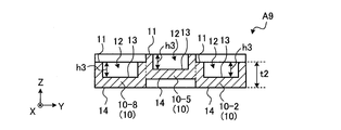
図9A~図9Cに示す発光素子搭載用アレイパッケージA9は、実施形態の他の態様8である。かかる他の態様8では、複数の発光素子搭載用パッケージ10が並んで設けられる場合に、それぞれの発光素子搭載用パッケージ10のおもて面11の高さが交互に異なる。
図9A~図9Cに示す発光素子搭載用アレイパッケージA9は、実施形態の他の態様8である。かかる他の態様8では、複数の発光素子搭載用パッケージ10が並んで設けられる場合に、それぞれの発光素子搭載用パッケージ10のおもて面11の高さが交互に異なる。
たとえば、おもて面11が高い位置にある発光素子搭載用パッケージ10-1、10-3、10-5、10-7、10-9と、おもて面11が低い位置にある発光素子搭載用パッケージ10-2、10-4、10-6、10-8とが、3行×3列のマトリックス状に並んで設けられる。
これにより、発光素子搭載用パッケージ10-1、10-3、10-5、10-7、10-9の搭載面13の高さを、隣接する発光素子搭載用パッケージ10-2、10-4、10-6、10-8の搭載面13の高さと異ならせることができる。また、発光素子搭載用パッケージ10-1、10-3、10-5、10-7、10-9と、隣接する発光素子搭載用パッケージ10-2、10-4、10-6、10-8とが互いに接しない露出面をすべての発光素子搭載用パッケージ10の側方に設けることができる。
したがって、他の態様8によれば、マトリックス状に並べられたすべての発光素子搭載用パッケージ10において、隣接する発光素子からの熱干渉を低減することができる。
なお、図9A~図9Cでは、発光素子搭載用パッケージ10-1、10-3、10-5、10-7、10-9のおもて面11を、隣接する発光素子搭載用パッケージ10-2、10-4、10-6、10-8のおもて面11より高い位置に配置した例について示している。
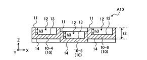
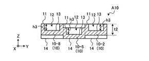
一方で、図10A~図10Cに示す他の態様9の発光素子搭載用アレイパッケージA10のように、発光素子搭載用パッケージ10-1、10-3、10-5、10-7、10-9のおもて面11を、隣接する発光素子搭載用パッケージ10-2、10-4、10-6、10-8のおもて面11より低い位置に設けてもよい。
(他の態様10)
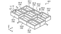
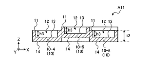
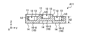
図11A~図11Cに示す発光素子搭載用アレイパッケージA11は、実施形態の他の態様10である。かかる他の態様10では、斜めに並んで配置される複数の発光素子搭載用パッケージ10のおもて面11の高さが、他の発光素子搭載用パッケージ10のおもて面11の高さと異なる。
図11A~図11Cに示す発光素子搭載用アレイパッケージA11は、実施形態の他の態様10である。かかる他の態様10では、斜めに並んで配置される複数の発光素子搭載用パッケージ10のおもて面11の高さが、他の発光素子搭載用パッケージ10のおもて面11の高さと異なる。
たとえば、おもて面11が高い位置にある発光素子搭載用パッケージ10-3、10-5、10-7が斜めに並んで設けられる。そして、かかる発光素子搭載用パッケージ10-3、10-5、10-7に隣接する発光素子搭載用パッケージ10-1、10-2、10-4、10-6、10-8、10-9は、おもて面11が低い位置に設けられる。
これにより、発光素子搭載用パッケージ10-3、10-5、10-7の搭載面13の高さを、隣接する発光素子搭載用パッケージ10-1、10-2、10-4、10-6、10-8、10-9の搭載面13の高さと異ならせることができる。また、隣接する発光素子搭載用パッケージ10-2、10-4、10-6、10-8に接しない露出面を発光素子搭載用パッケージ10-3、10-5、10-7の側方に設けることができる。
したがって、他の態様10によれば、マトリックス状に複数の発光素子搭載用パッケージ10を並べた場合に、斜めに並んで配置される複数の発光素子搭載用パッケージ10の放熱性を高めることができる。
なお、かかる他の態様10では、発光素子搭載用パッケージ10-3、10-5、10-7のおもて面11を、隣接する発光素子搭載用パッケージ10-1、10-2、10-4、10-6、10-8、10-9のおもて面11より低い位置に設けてもよい。
(他の態様11)
図12Aおよび図12Bに示す発光素子搭載用アレイパッケージA12は、実施形態の他の態様11である。かかる他の態様11では、発光素子搭載用パッケージ10-1~10-9に凹部12ではなく凸部12Aが形成されている点が実施形態と異なる。
図12Aおよび図12Bに示す発光素子搭載用アレイパッケージA12は、実施形態の他の態様11である。かかる他の態様11では、発光素子搭載用パッケージ10-1~10-9に凹部12ではなく凸部12Aが形成されている点が実施形態と異なる。
他の態様11に係る発光素子搭載用パッケージ10はおもて面11を有し、かかるおもて面11に凸部12Aが形成される。また、すべての発光素子搭載用パッケージ10において、おもて面11は同じ向き(図ではZ軸正方向)に向いている。そして、すべての発光素子搭載用パッケージ10のおもて面11が略面一である。
また、発光素子搭載用パッケージ10に形成される凸部12Aの上面には、図示しない発光素子を搭載する搭載面13が設けられる。
そして、他の態様11では、凸部12Aの高さが異なる発光素子搭載用パッケージ10が交互に並んで配置される。たとえば、凸部12Aが高さh1Aである発光素子搭載用パッケージ10-1と、凸部12Aが高さh2Aである発光素子搭載用パッケージ10-2と、凸部12Aが高さh1Aである発光素子搭載用パッケージ10-3とがX軸方向に並んで配置される。
また、凸部12Aが高さh2Aである発光素子搭載用パッケージ10-4と、凸部12Aが高さh1Aである発光素子搭載用パッケージ10-5と、凸部12Aが高さh2Aである発光素子搭載用パッケージ10-6とがX軸方向に並んで配置される。
さらに、凸部12Aが高さh1Aである発光素子搭載用パッケージ10-7と、凸部12Aが高さh2Aである発光素子搭載用パッケージ10-8と、凸部12Aが高さh1Aである発光素子搭載用パッケージ10-9とがX軸方向に並んで配置される。
これにより、並んで配置される発光素子搭載用パッケージ10の間で、搭載面13と平行な方向において、搭載される発光素子から発生する熱で高温になる高さの位置を交互に変えることができる。したがって、他の態様11によれば、複数の発光素子が並んで設けられる場合に、隣接する発光素子からの熱干渉をさらに低減することができる。
また、他の態様11では、図12Aに示すように、X軸方向のみならずY軸方向においても、凸部12Aの高さが異なる発光素子搭載用パッケージ10が交互に並んで配置されるとよい。これにより、複数の発光素子がマトリックス状に並んで設けられる場合に、隣接する発光素子からの熱干渉を低減することができる。
なお、他の態様11では、凸部12Aの高さがX軸方向およびY軸方向において異なる発光素子搭載用パッケージ10が交互に並んで配置される場合に限られず、少なくとも1つの発光素子搭載用パッケージ10の搭載面13の高さが、他の発光素子搭載用パッケージ10の搭載面13の高さと異なっていればよい。
たとえば、発光素子搭載用パッケージ10-5の搭載面13の高さが、他の発光素子搭載用パッケージ10-1~10-4、10-6~10-9の搭載面13の高さより高くなっていてもよい。
<発光素子搭載用アレイパッケージの製造方法>
次に、実施形態に係る発光素子搭載用アレイパッケージA1の製造方法について、図13および図14を参照しながら説明する。発光素子搭載用アレイパッケージA1は、グリーンシート50に所定の加工および成形を施した後に、成形体を焼成して形成される。
次に、実施形態に係る発光素子搭載用アレイパッケージA1の製造方法について、図13および図14を参照しながら説明する。発光素子搭載用アレイパッケージA1は、グリーンシート50に所定の加工および成形を施した後に、成形体を焼成して形成される。
以下においては、グリーンシート50の前半の各工程を図13に基づいて説明し、グリーンシート50の後半の各工程を図14に基づいて説明する。
図13の(a)に示すように、あらかじめ所定の形状に加工したグリーンシート50を用意し、グリーンシート50の所定の18カ所を平面視で円状に打ち抜いて、打ち抜いた18個の孔部をそれぞれビア導体51a1~51i1、51a2~51i2で埋める。
次に、図13の(b)に示すように、グリーンシート50の上面に、ビア導体51a1~51i1、51a2~51i2とそれぞれつながるように導体パターン52a1~52i1、52a2~52i2を印刷する。そして、図13の(c)に示すように、グリーンシート50の下面に、ビア導体51a1~51i1、51a2~51i2とそれぞれつながるように導体パターン53a1~53i1、53a2~53i2を印刷する。
以後の工程を示す図14は、図13の(c)に示すS-S線の矢視断面図である。図14の(a)に示すように、グリーンシート50を収容可能な凹部101aが形成された上金型101と、平板状の下金型102とで挟み込んだグリーンシート50に加熱加圧を行い、成形体60を形成する(図14の(b))。
なお、上金型101の凹部101aには、所定の位置で大きく突出する凸部101bと、所定の位置で小さく突出する複数の凸部101cとが設けられる。
ここで、凸部101bによって形成される成形体60の凹部54aは、発光素子搭載用パッケージ10-5に形成される深さh1の凹部12に対応する部位であり、凸部101cによって形成される複数の凹部54bは、発光素子搭載用パッケージ10-1~10-4、10-6~10-9に形成される深さh2の凹部12に対応する部位である。
ここで、導体パターン52d1、53d1は、発光素子搭載用パッケージ10-4の素子用端子および電源用端子に対応する部位であり、導体パターン52e1、53e1は、発光素子搭載用パッケージ10-5の素子用端子および電源用端子に対応する部位であり、導体パターン52f1、53f1は、発光素子搭載用パッケージ10-6の素子用端子および電源用端子に対応する部位である。
また、ビア導体51d1は、発光素子搭載用パッケージ10-4の素子用端子および電源用端子を接続するビア導体に対応する部位であり、ビア導体51e1は、発光素子搭載用パッケージ10-5の素子用端子および電源用端子を接続するビア導体に対応する部位であり、ビア導体51f1は、発光素子搭載用パッケージ10-6の素子用端子および電源用端子を接続するビア導体に対応する部位である。
なお、図14には図示していないが、導体パターン52a1、52a2は、発光素子搭載用パッケージ10-1の1対の素子用端子に対応する部位であり、導体パターン53a1、53a2は、発光素子搭載用パッケージ10-1の1対の電源用端子に対応する部位である。また、ビア導体51a1、51a2は、発光素子搭載用パッケージ10-1の1対の素子用端子と1対の電源用端子とをそれぞれ接続する1対のビア導体に対応する部位である。
また、導体パターン52b1、52b2は、発光素子搭載用パッケージ10-2の1対の素子用端子に対応する部位であり、導体パターン53b1、53b2は、発光素子搭載用パッケージ10-2の1対の電源用端子に対応する部位である。また、ビア導体51b1、51b2は、発光素子搭載用パッケージ10-2の1対の素子用端子と1対の電源用端子とをそれぞれ接続する1対のビア導体に対応する部位である。
また、導体パターン52c1、52c2は、発光素子搭載用パッケージ10-3の1対の素子用端子に対応する部位であり、導体パターン53c1、53c2は、発光素子搭載用パッケージ10-3の1対の電源用端子に対応する部位である。また、ビア導体51c1、51c2は、発光素子搭載用パッケージ10-3の1対の素子用端子と1対の電源用端子とをそれぞれ接続する1対のビア導体に対応する部位である。
また、導体パターン52d2、53d2は、発光素子搭載用パッケージ10-4のもう一方の素子用端子および電源用端子に対応する部位であり、導体パターン52e2、53e2は、発光素子搭載用パッケージ10-5のもう一方の素子用端子および電源用端子に対応する部位であり、導体パターン52f2、53f2は、発光素子搭載用パッケージ10-6のもう一方の素子用端子および電源用端子に対応する部位である。
また、ビア導体51d2は、発光素子搭載用パッケージ10-4のもう一方の素子用端子および電源用端子を接続するビア導体に対応する部位であり、ビア導体51e2は、発光素子搭載用パッケージ10-5のもう一方の素子用端子および電源用端子を接続するビア導体に対応する部位であり、ビア導体51f2は、発光素子搭載用パッケージ10-6のもう一方の素子用端子および電源用端子を接続するビア導体に対応する部位である。
また、導体パターン52g1、52g2は、発光素子搭載用パッケージ10-7の1対の素子用端子に対応する部位であり、導体パターン53g1、53g2は、発光素子搭載用パッケージ10-7の1対の電源用端子に対応する部位である。また、ビア導体51g1、51g2は、発光素子搭載用パッケージ10-7の1対の素子用端子と1対の電源用端子とをそれぞれ接続する1対のビア導体に対応する部位である。
また、導体パターン52h1、52h2は、発光素子搭載用パッケージ10-8の1対の素子用端子に対応する部位であり、導体パターン53h1、53h2は、発光素子搭載用パッケージ10-8の1対の電源用端子に対応する部位である。また、ビア導体51h1、51h2は、発光素子搭載用パッケージ10-8の1対の素子用端子と1対の電源用端子とをそれぞれ接続する1対のビア導体に対応する部位である。
また、導体パターン52i1、52i2は、発光素子搭載用パッケージ10-9の1対の素子用端子に対応する部位であり、導体パターン53i1、53i2は、発光素子搭載用パッケージ10-9の1対の電源用端子に対応する部位である。また、ビア導体51i1、51i2は、発光素子搭載用パッケージ10-9の1対の素子用端子と1対の電源用端子とをそれぞれ接続する1対のビア導体に対応する部位である。
そして、製造工程の最後に、図14の(b)のように形成された成形体60を高温(1500℃~1900℃)で焼成して、図1Aなどに示した発光素子搭載用アレイパッケージA1が完成する。
上述の製造工程に用いられるグリーンシート50は、たとえば、主原料である窒化アルミニウムの粉体に、イットリア(Y2O3)、カルシア(CaO)、エルビア(Er2O3)などからなる粉体を焼結助剤として混合した無機粉体を基本構成とする。そして、かかる無機粉体に有機ビヒクルを添加混合して泥漿状となすとともに、これを従来周知のドクターブレード法やカレンダーロール法を用いることにより、グリーンシート50が形成される。
また、導体パターン52a1~52i1、52a2~52i2、53a1~53i1、53a2~53i2や、ビア導体51a1~51i1、51a2~51i2は、たとえば、主原料である高融点金属のモリブデン(Mo)またはタングステン(W)に、窒化アルミニウム、有機バインダー、溶剤などを共剤として混合したペーストで形成される。なお、セラミックスの焼成温度によっては、上記の高融点金属に銅などの低融点金属を含ませたものを用いてもよい。
また、上述した他の態様の発光素子搭載用アレイパッケージA2~A12についても、上金型101および下金型102の形状等を変更することで同様に作製することができる。
以下、実施形態に係る発光素子搭載用アレイパッケージA1、A5を具体的に作製し、次いで、かかる発光素子搭載用アレイパッケージA1、A5を適用した発光装置を作製した。なお、参考例として、図15A~図15Cに示す発光素子搭載用アレイパッケージB1も具体的に作製した。
図15A~図15Cに示す発光素子搭載用アレイパッケージB1は、複数(図では9個)の発光素子搭載用パッケージ10に設けられるおもて面11の高さおよび凹部12の深さがすべて等しい点が実施形態と異なる。すなわち、図15A~図15Cに示す参考例は、すべての発光素子搭載用パッケージ10-1~10-9の搭載面13の高さが等しくなっている。
まず、グリーンシートを形成するための混合粉末として、窒化アルミニウム粉末94質量%に対して、イットリア粉末を5質量%、カルシア粉末を1質量%の割合で混合した混合粉末を調製した。
次に、この混合粉末(固形分)100質量部に対して、有機バインダーとしてアクリル系バインダーを20質量部、トルエンを50質量部添加してスラリーを調製し、次に、ドクターブレード法を用いて、平均厚みが500μmのグリーンシートを作製した。
また、導体パターンやビア導体などの導体の形成には、タングステン粉末100質量部に対して、窒化アルミニウム粉末を20質量部、アクリル系バインダーを8質量部、テルピネオールを適宜添加した導体ペーストを用いた。また、この導体ペーストの他に、この導体ペーストにさらにチキソ剤を0.5質量%添加した導体ペーストと、この導体ペーストにさらにチキソ剤を1.0質量%添加した導体ペーストも用いた。
そして、上述の成分を有するグリーンシートおよび導体ペーストを用いて、図13、図14に示した製造方法で成形体60(図14の(b)参照)を作製した。
次に、作製した成形体60を還元雰囲気中、最高温度が1800℃となる条件にて2時間の焼成を行って発光素子搭載用アレイパッケージA1、A5、B1を作製した。なお、作製された発光素子搭載用アレイパッケージA1、B1のサイズは、焼成後の形状で幅15mm×長さ15mm×高さ5mmであった。また、作製された発光素子搭載用アレイパッケージA5のサイズは、焼成後の形状で幅15mm×長さ15mm×高さ7.5mmであった。
また、発光素子搭載用アレイパッケージA1において、発光素子搭載用パッケージ10-1~10-4、10-6~10-9に形成される凹部12の大きさは、幅3mm×長さ3mm×深さ3mmであり、発光素子搭載用パッケージ10-5に形成される凹部12の大きさは、幅3mm×長さ3mm×深さ4mmであった。
また、発光素子搭載用アレイパッケージA5において、発光素子搭載用パッケージ10-1~10-9に形成される凹部12の大きさは、幅3mm×長さ3mm×深さ3mmであり、発光素子搭載用パッケージ10-5は、その他の発光素子搭載用パッケージ10-1~10-4、10-6~10-9に対して0.5mm上側に突出していた。
また、発光素子搭載用アレイパッケージB1において、発光素子搭載用パッケージ10-1~10-9に形成される凹部12の大きさは、幅3mm×長さ3mm×深さ3mmであった。
次に、発光素子搭載用アレイパッケージA1、A5、B1の搭載面13に発光素子を実装した。ここで、発光素子としてはSi製の半導体素子(幅2.5mm×長さ2.5mm×高さ0.3mm)を用い、搭載面13に設けられる素子用端子への発光素子の接合にはAu-Snハンダを用いた。なお、搭載面13に設けられる素子用端子のサイズは、搭載される発光素子のサイズと同等のサイズとした。
次に、発光素子搭載用アレイパッケージA1、A5、B1の放熱性について評価した。かかる放熱性の評価は、まず、25℃の大気中で試験用の半導体素子(幅0.5mm×長さ1.5mm×高さ0.3mm)に1Wの電流を1分間通電した。
この後、通電を止め、10秒後に半導体素子の表面の温度(℃)を熱電対によって測定した。評価結果を表1に示す。なお、表1には、試料1(発光素子搭載用アレイパッケージB1)が示した温度(最高温度)と25℃との温度差を1としたときの相対比を示す。

すべての発光素子搭載用パッケージ10-1~10-9の搭載面13の高さが等しくなっている試料1と、発光素子搭載用パッケージ10-5の搭載面13の高さがその他の発光素子搭載用パッケージ10-1~10-4、10-6~10-9の搭載面13の高さと異なっている試料2、3との比較により、搭載面13の高さを異ならせることによって放熱性が向上していることがわかる。
以上、本発明の実施形態について説明したが、本発明は上記実施形態に限定されるものではなく、その趣旨を逸脱しない限りにおいて種々の変更が可能である。たとえば、上述の実施形態では、複数の発光素子搭載用パッケージ10がマトリックス上に並んだ発光素子搭載用アレイパッケージA1~A12について示したが、複数の発光素子搭載用パッケージ10が一列に並んだ発光素子搭載用アレイパッケージに上述の実施形態を適用してもよい。
以上のように、実施形態に係る電気素子搭載用アレイパッケージ(発光素子搭載用アレイパッケージA1~A12)は、電気素子(発光素子)の搭載面13を有する電気素子搭載用パッケージ(発光素子搭載用パッケージ10)が複数並んで設けられ、少なくとも1つの電気素子搭載用パッケージ(発光素子搭載用パッケージ10)の搭載面13の高さが、他の電気素子搭載用パッケージ(発光素子搭載用パッケージ10)の搭載面13の高さと異なる。これにより、複数の発光素子が並んで設けられる場合に、隣接する発光素子からの熱干渉を低減することができる。
また、実施形態に係る電気素子搭載用アレイパッケージ(発光素子搭載用アレイパッケージA1~A11)において、電気素子搭載用パッケージ(発光素子搭載用パッケージ10)は、おもて面11に開口し、搭載面13を底部に備えた凹部12を有する。これにより、発光素子の周囲に形成される堤部からの放熱が可能となることができることから、発光素子搭載用アレイパッケージA1~A11の放熱性を向上させることができる。
また、実施形態に係る電気素子搭載用アレイパッケージ(発光素子搭載用アレイパッケージA2、A3)において、凹部12の深さが異なる電気素子搭載用パッケージ(発光素子搭載用パッケージ10)が交互に並んで配置される。これにより、複数の発光素子が並んで設けられる場合に、隣接する発光素子からの熱干渉をさらに低減することができる。
また、実施形態に係る電気素子搭載用アレイパッケージ(発光素子搭載用アレイパッケージA4~A11)において、少なくとも1つの電気素子搭載用パッケージ(発光素子搭載用パッケージ10)のおもて面11の高さが、他の電気素子搭載用パッケージ(発光素子搭載用パッケージ10)のおもて面11の高さと異なる。これにより、放熱性の高い発光素子搭載用アレイパッケージA4~A11を実現することができる。
また、実施形態に係る電気素子搭載用アレイパッケージ(発光素子搭載用アレイパッケージA3)において、少なくとも1つの電気素子搭載用パッケージ(発光素子搭載用パッケージ10)の凹部12は、隣接する電気素子搭載用パッケージ(発光素子搭載用パッケージ10)の凹部12に対して水平方向にずれている。これにより、複数の発光素子が並んで設けられる場合に、隣接する発光素子からの熱干渉をさらに低減することができる。
また、実施形態に係る電気素子搭載用アレイパッケージ(発光素子搭載用アレイパッケージA3)において、複数の電気素子搭載用パッケージ(発光素子搭載用パッケージ10)が千鳥状に配置される。これにより、発光光度の高い場所と低い場所の強弱が小さくなるため、一様な明るさの発光装置を実現することができる。
また、実施形態に係る電気素子搭載用アレイパッケージ(発光素子搭載用アレイパッケージA1~A12)において、複数の電気素子搭載用パッケージ(発光素子搭載用パッケージ10)がマトリックス状に配置される。これにより、面状に発光可能な発光装置を実現することができる。
また、実施形態に係る電気素子搭載用アレイパッケージ(発光素子搭載用アレイパッケージA5)において、マトリックス状に配置される複数の電気素子搭載用パッケージ(発光素子搭載用パッケージ10)の中央部に配置される電気素子搭載用パッケージ(発光素子搭載用パッケージ10)が上側または下側に突出する。これにより、周辺部に比べて熱干渉が生じやすい中央部に配置される発光素子搭載用パッケージ10において、隣接する発光素子からの熱干渉をさらに低減することができる。
また、実施形態に係る電気素子搭載用アレイパッケージ(発光素子搭載用アレイパッケージA6)において、行方向に並んで配置される複数の電気素子搭載用パッケージ(発光素子搭載用パッケージ10)のおもて面11の高さが、列方向に隣接する複数の電気素子搭載用パッケージ(発光素子搭載用パッケージ10)のおもて面11の高さと異なる。これにより、マトリックス状に複数の発光素子搭載用パッケージ10を並べた場合に、行ごとに放熱性を高めることができる。
また、実施形態に係る電気素子搭載用アレイパッケージ(発光素子搭載用アレイパッケージA8)において、十字状に並んで配置される複数の電気素子搭載用パッケージ(発光素子搭載用パッケージ10)のおもて面11の高さが、隣接する複数の電気素子搭載用パッケージ(発光素子搭載用パッケージ10)のおもて面11の高さと異なる。これにより、角部に比べて熱干渉が生じやすい発光素子搭載用パッケージ10-2、10-4~10-6、10-8において、隣接する発光素子からの熱干渉を低減することができる。
また、実施形態に係る電気素子搭載用アレイパッケージ(発光素子搭載用アレイパッケージA9、A10)において、複数の電気素子搭載用パッケージ(発光素子搭載用パッケージ10)のおもて面11の高さが交互に異なる。これにより、マトリックス状に並べられたすべての発光素子搭載用パッケージ10において、隣接する発光素子からの熱干渉を低減することができる。
また、実施形態に係る電気素子搭載用アレイパッケージ(発光素子搭載用アレイパッケージA11)において、斜めに並んで配置される複数の電気素子搭載用パッケージ(発光素子搭載用パッケージ10)のおもて面11の高さが、隣接する複数の電気素子搭載用パッケージ(発光素子搭載用パッケージ10)のおもて面11の高さと異なる。これにより、マトリックス状に複数の発光素子搭載用パッケージ10を並べた場合に、斜めに並んで配置される複数の発光素子搭載用パッケージ10の放熱性を高めることができる。
また、実施形態に係る電気装置(発光装置)は、上記に記載の電気素子搭載用アレイパッケージ(発光素子搭載用アレイパッケージA1~A12)と、複数の電気素子搭載用パッケージ(発光素子搭載用パッケージ10)の搭載面13にそれぞれ搭載される複数の電気素子(発光素子)と、を備える。これにより、複数の発光素子が並んで設けられる場合に、隣接する発光素子からの熱干渉を低減することができる。
さらなる効果や他の態様は、当業者によって容易に導き出すことができる。このため、本発明のより広範な態様は、以上のように表しかつ記述した特定の詳細および代表的な実施形態に限定されるものではない。したがって、添付の請求の範囲およびその均等物によって定義される総括的な発明の概念の精神または範囲から逸脱することなく、様々な変更が可能である。
A1~A12 発光素子搭載用アレイパッケージ
10、10-1~10-9 発光素子搭載用パッケージ
11 おもて面
12 凹部
13 搭載面
14 裏面
10、10-1~10-9 発光素子搭載用パッケージ
11 おもて面
12 凹部
13 搭載面
14 裏面
Claims (13)
- 電気素子の搭載面を有する電気素子搭載用パッケージが複数並んで設けられ、
少なくとも1つの前記電気素子搭載用パッケージの前記搭載面の高さが、他の前記電気素子搭載用パッケージの前記搭載面の高さと異なる
電気素子搭載用アレイパッケージ。 - 前記電気素子搭載用パッケージは、おもて面に開口し、前記搭載面を底部に備えた凹部を有する
請求項1に記載の電気素子搭載用アレイパッケージ。 - 前記凹部の深さが異なる前記電気素子搭載用パッケージが交互に並んで配置される
請求項2に記載の電気素子搭載用アレイパッケージ。 - 少なくとも1つの前記電気素子搭載用パッケージのおもて面の高さが、他の前記電気素子搭載用パッケージのおもて面の高さと異なる
請求項2または3に記載の電気素子搭載用アレイパッケージ。 - 少なくとも1つの前記電気素子搭載用パッケージの前記凹部は、隣接する前記電気素子搭載用パッケージの前記凹部に対して水平方向にずれている
請求項2~4のいずれか一つに記載の電気素子搭載用アレイパッケージ。 - 複数の前記電気素子搭載用パッケージが千鳥状に配置される
請求項1~5のいずれか一つに記載の電気素子搭載用アレイパッケージ。 - 複数の前記電気素子搭載用パッケージがマトリックス状に配置される
請求項1~5のいずれか一つに記載の電気素子搭載用アレイパッケージ。 - マトリックス状に配置される複数の前記電気素子搭載用パッケージの中央部に配置される前記電気素子搭載用パッケージが上側または下側に突出する
請求項7に記載の電気素子搭載用アレイパッケージ。 - 行方向に並んで配置される複数の前記電気素子搭載用パッケージのおもて面の高さが、列方向に隣接する複数の前記電気素子搭載用パッケージのおもて面の高さと異なる
請求項7に記載の電気素子搭載用アレイパッケージ。 - 十字状に並んで配置される複数の前記電気素子搭載用パッケージのおもて面の高さが、隣接する複数の前記電気素子搭載用パッケージのおもて面の高さと異なる
請求項7に記載の電気素子搭載用アレイパッケージ。 - 複数の前記電気素子搭載用パッケージのおもて面の高さが交互に異なる
請求項6または7に記載の電気素子搭載用アレイパッケージ。 - 斜めに並んで配置される複数の前記電気素子搭載用パッケージのおもて面の高さが、隣接する複数の前記電気素子搭載用パッケージのおもて面の高さと異なる
請求項7に記載の電気素子搭載用アレイパッケージ。 - 請求項1~12のいずれか一つに記載の電気素子搭載用アレイパッケージと、
複数の前記電気素子搭載用パッケージの前記搭載面にそれぞれ搭載される複数の電気素子と、
を備える電気装置。
Priority Applications (1)
| Application Number | Priority Date | Filing Date | Title |
|---|---|---|---|
| JP2020557603A JPWO2020110867A1 (ja) | 2018-11-26 | 2019-11-20 | 電気素子搭載用アレイパッケージおよび電気装置 |
Applications Claiming Priority (2)
| Application Number | Priority Date | Filing Date | Title |
|---|---|---|---|
| JP2018220545 | 2018-11-26 | ||
| JP2018-220545 | 2018-11-26 |
Publications (1)
| Publication Number | Publication Date |
|---|---|
| WO2020110867A1 true WO2020110867A1 (ja) | 2020-06-04 |
Family
ID=70852883
Family Applications (1)
| Application Number | Title | Priority Date | Filing Date |
|---|---|---|---|
| PCT/JP2019/045514 Ceased WO2020110867A1 (ja) | 2018-11-26 | 2019-11-20 | 電気素子搭載用アレイパッケージおよび電気装置 |
Country Status (2)
| Country | Link |
|---|---|
| JP (1) | JPWO2020110867A1 (ja) |
| WO (1) | WO2020110867A1 (ja) |
Citations (4)
| Publication number | Priority date | Publication date | Assignee | Title |
|---|---|---|---|---|
| JP2009206466A (ja) * | 2008-01-30 | 2009-09-10 | Kyocera Corp | 発光素子収納用パッケージおよび発光装置 |
| JP3156826U (ja) * | 2009-11-02 | 2010-01-21 | 柏友照明科技股▲フン▼有限公司 | 所定形状の面光源になるように任意に組合せ可能な発光モジュール |
| JP2010199274A (ja) * | 2009-02-25 | 2010-09-09 | Nichia Corp | 半導体レーザ装置 |
| WO2016010094A1 (ja) * | 2014-07-15 | 2016-01-21 | シチズン電子株式会社 | 発光装置 |
-
2019
- 2019-11-20 WO PCT/JP2019/045514 patent/WO2020110867A1/ja not_active Ceased
- 2019-11-20 JP JP2020557603A patent/JPWO2020110867A1/ja active Pending
Patent Citations (4)
| Publication number | Priority date | Publication date | Assignee | Title |
|---|---|---|---|---|
| JP2009206466A (ja) * | 2008-01-30 | 2009-09-10 | Kyocera Corp | 発光素子収納用パッケージおよび発光装置 |
| JP2010199274A (ja) * | 2009-02-25 | 2010-09-09 | Nichia Corp | 半導体レーザ装置 |
| JP3156826U (ja) * | 2009-11-02 | 2010-01-21 | 柏友照明科技股▲フン▼有限公司 | 所定形状の面光源になるように任意に組合せ可能な発光モジュール |
| WO2016010094A1 (ja) * | 2014-07-15 | 2016-01-21 | シチズン電子株式会社 | 発光装置 |
Also Published As
| Publication number | Publication date |
|---|---|
| JPWO2020110867A1 (ja) | 2021-10-14 |
Similar Documents
| Publication | Publication Date | Title |
|---|---|---|
| JP6884823B2 (ja) | 電気素子搭載用パッケージ、アレイ型パッケージおよび電気装置 | |
| EP2182783A2 (en) | Light-emitting module and illuminating apparatus | |
| EP1819963A1 (en) | Light emitting module, lighting device, and display device | |
| CN109075526B (zh) | 发光元件收纳用构件及发光装置 | |
| CN111095698B (zh) | 发光元件收纳用构件、阵列构件及发光装置 | |
| WO2020110867A1 (ja) | 電気素子搭載用アレイパッケージおよび電気装置 | |
| CN112970103B (zh) | 布线基板、复合基板以及电气装置 | |
| JP7148276B2 (ja) | 発光素子搭載用パッケージおよび発光装置 | |
| TWI765161B (zh) | 電氣元件搭載用封裝體、陣列型封裝體及電氣裝置 | |
| CN112753143B (zh) | 发光元件搭载用基板、阵列基板以及发光装置 | |
| CN112805821B (zh) | 电子部件搭载用基板、电气装置以及发光装置 | |
| CN103441192A (zh) | 发光二极管封装体及其封装方法 |
Legal Events
| Date | Code | Title | Description |
|---|---|---|---|
| 121 | Ep: the epo has been informed by wipo that ep was designated in this application |
Ref document number: 19890560 Country of ref document: EP Kind code of ref document: A1 |
|
| ENP | Entry into the national phase |
Ref document number: 2020557603 Country of ref document: JP Kind code of ref document: A |
|
| NENP | Non-entry into the national phase |
Ref country code: DE |
|
| 122 | Ep: pct application non-entry in european phase |
Ref document number: 19890560 Country of ref document: EP Kind code of ref document: A1 |